Digital Logic Design and Application ( 数字逻辑设计及应用 )
159
1 Digital Logic Design and Application ( 数数数数数数数数数 ) Review of Chapter 2 ( 数数数数数数数 ) General Positional-Number-System Conversion ( 数数数数数数数数数数 ) Addition and Subtraction of Non- decimal Numbers ( 数数数数数数数数数数 )
-
Upload
marah-casey -
Category
Documents
-
view
142 -
download
6
description
Digital Logic Design and Application ( 数字逻辑设计及应用 ). Review of Chapter 2 ( 第二章内容回顾 ). General Positional-Number-System Conversion ( 常用按位计数制的转换 ) Addition and Subtraction of Non-decimal Numbers ( 非十进制的加法和减法 ). Digital Logic Design and Application ( 数字逻辑设计及应用 ). - PowerPoint PPT Presentation
Transcript of Digital Logic Design and Application ( 数字逻辑设计及应用 )
1
Digital Logic Design and Application ( 数字逻辑设计及应用 )
Review of Chapter 2 (第二章内容回顾 )
General Positional-Number-System
Conversion
(常用按位计数制的转换 )
Addition and Subtraction of Non-decimal Numbers
(非十进制的加法和减法 )
2
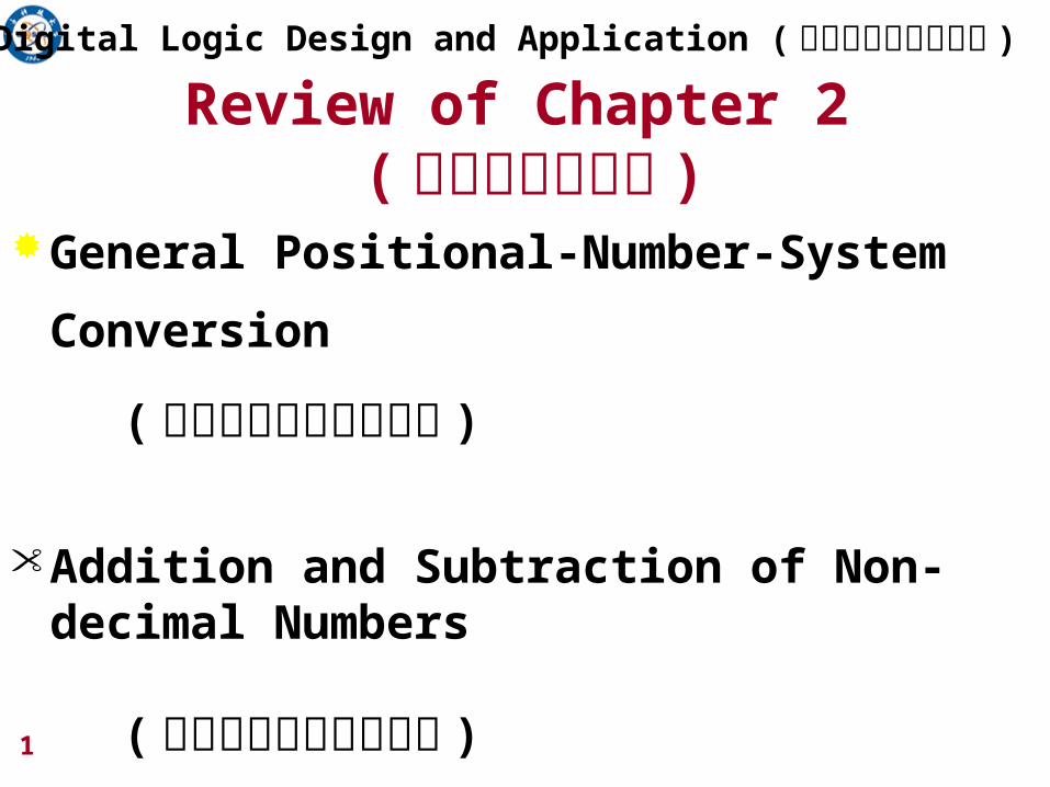
Review of Chapter 2 (第二章内容回顾 )
Representation of Negative Numbers (负数的表示 )
Signed-Magnitude [ 符号-数值(原码) ]Complement Number Systems (补码数制 )
Radix – Complement (基数补码 )
Diminished Radix – Complement
[ 基数减 1补码(基数反码) ]
Digital Logic Design and Application ( 数字逻辑设计及应用 )
3
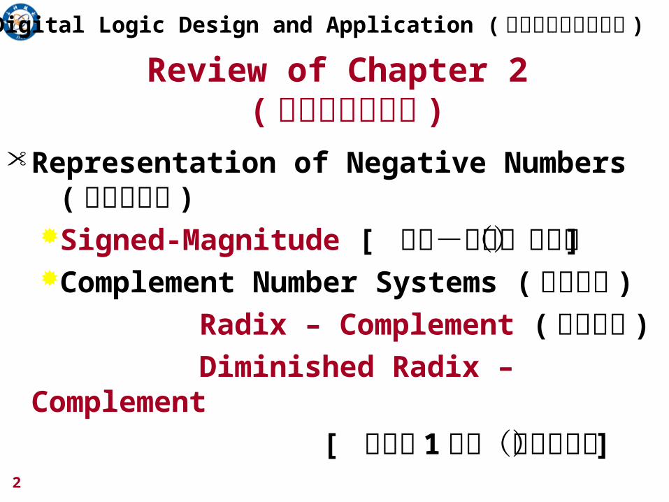
Review of Chapter 2 (第二章内容回顾 )
Binary Signed-Magnitude, Ones’ – Complement, and Two’s – Complement Representation
(二进制的原码、反码、补码表示 )
直接由补码 (反码 )求二进制数值的大 小:最高位位权为 -2n-1 (-2n-1 -1)
(1011)2补= ( ) 10
Digital Logic Design and Application ( 数字逻辑设计及应用 )
4
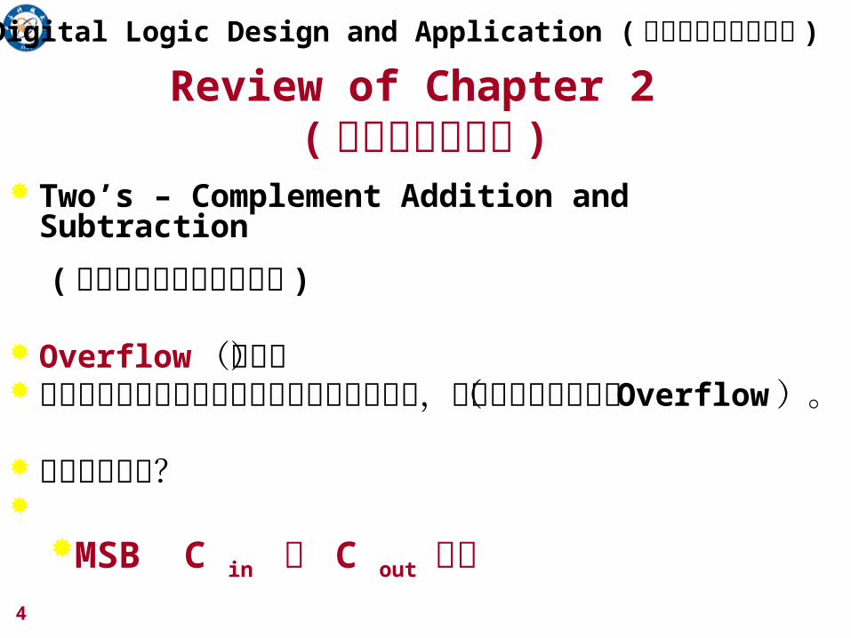
Review of Chapter 2 (第二章内容回顾 )
Two’s – Complement Addition and Subtraction
(二进制补码的加法和减法 )
Overflow(溢出)如果加法运算产生的和超出了数制表示的范围,则结果发生了溢出( Overflow)。
如何判断溢出?
MSB C in 与 C out 不同
Digital Logic Design and Application ( 数字逻辑设计及应用 )
5
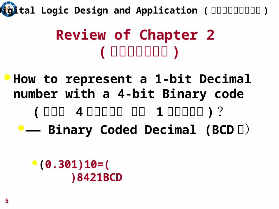
Review of Chapter 2 (第二章内容回顾 )
How to represent a 1-bit Decimal number with a 4-bit Binary code
( 如何用 4 位二进制码 表示 1位十进制码 )?—— Binary Coded Decimal (BCD码)
(0.301)10=( )8421BCD
Digital Logic Design and Application ( 数字逻辑设计及应用 )
6
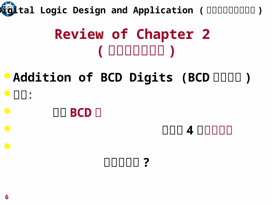
Review of Chapter 2 (第二章内容回顾 )
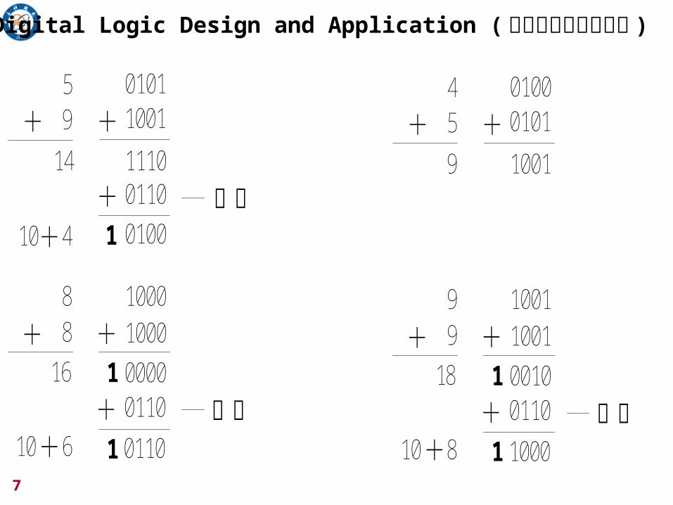
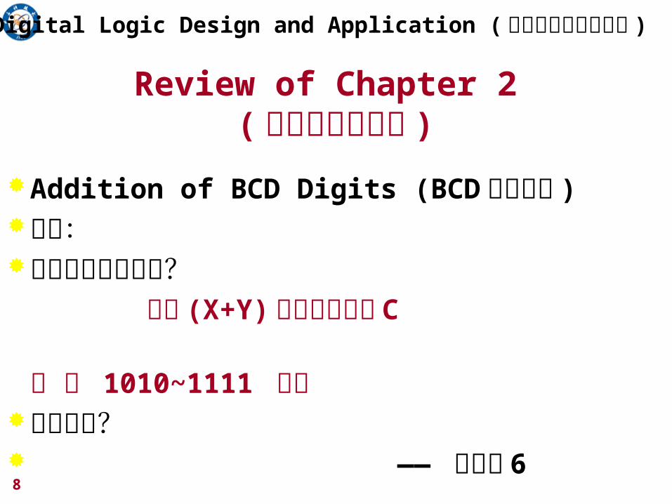
Addition of BCD Digits (BCD数的加法 )思考: 两个 BCD码 与两个 4位二进制数 相加的区别 ?
Digital Logic Design and Application ( 数字逻辑设计及应用 )
7
Digital Logic Design and Application ( 数字逻辑设计及应用 )
01011001
11100110
0100
10001000
00000110
0110
59
14
10
88
16
10+
++
++
+ +
4 1
+6
1
1
修正
修正
01000101
1001
10011001
00100110
1000
45
9
99
18
10+
++
+ +
+8
1
1
修正
8
Review of Chapter 2 (第二章内容回顾 )
Addition of BCD Digits (BCD数的加法 )思考:何时需要进行修正? 如果 (X+Y)产生进位信号 C
或 在 1010~1111 之间
如何修正? —— 结果加 6
Digital Logic Design and Application ( 数字逻辑设计及应用 )
9
Review of Chapter 2 (第二章内容回顾 )
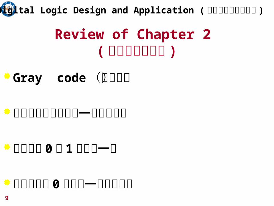
Gray code(格雷码)
任意相邻码字间只有一位数位变化
最高位的 0和 1只改变一次
最大数回到 0也只有一位码元不同
Digital Logic Design and Application ( 数字逻辑设计及应用 )
10
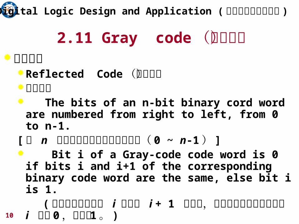
2.11 Gray code(格雷码)
Digital Logic Design and Application ( 数字逻辑设计及应用 )
构造方法Reflected Code(反射码)直接构造 The bits of an n-bit binary cord word are
numbered from right to left, from 0 to n-1. [ 对 n 位二进制的码字从右到左编号( 0 ~ n-1) ] Bit i of a Gray-code code word is 0 if bits i and
i+1 of the corresponding binary code word are the same, else bit i is 1.
( 若二进制码字的第 i 位和第 i + 1 位相同,则对 应的葛莱码码字的第 i 位为 0,否则为 1。 )
11
Review of Chapter 2 (第二章内容回顾 )
Digital Logic Design and Application ( 数字逻辑设计及应用 )
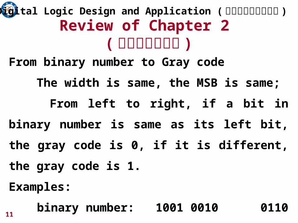
From binary number to Gray code
The width is same, the MSB is same;
From left to right, if a bit in binary number is same as
its left bit, the gray code is 0, if it is different, the gray
code is 1.
Examples:
binary number: 1001 0010 0110 0011
Gray code: 1101 1011 0101 0010
12
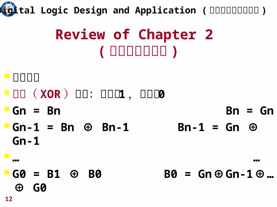
Review of Chapter 2 (第二章内容回顾 )
构造方法异或( XOR)运算:相异为 1,相同为 0Gn = Bn Bn = GnGn-1 = Bn Bn-1 Bn-1 = Gn Gn-1 ⊕ ⊕… … G0 = B1 B0 B0 = Gn Gn-1 … G0 ⊕ ⊕ ⊕ ⊕
Digital Logic Design and Application ( 数字逻辑设计及应用 )
13
Chapter 3 Digital Circuits (数字电路 )
Give a knowledge of the Electrical aspects of Digital Circuits
(介绍数字电路中的电气知识 )
Digital Logic Design and Application ( 数字逻辑设计及应用 )
14
Consider some Questions(思考几个问题)
在模拟的世界中如何表征数字系统?如何将物理上的实际值 映射为逻辑上的 0 和 1 ?什么时候考虑器件的逻辑功能; 什么时候考虑器件的模拟特性?
Digital Logic Design and Application ( 数字逻辑设计及应用 )
15
Digital Logic Design and Application ( 数字逻辑设计及应用 )
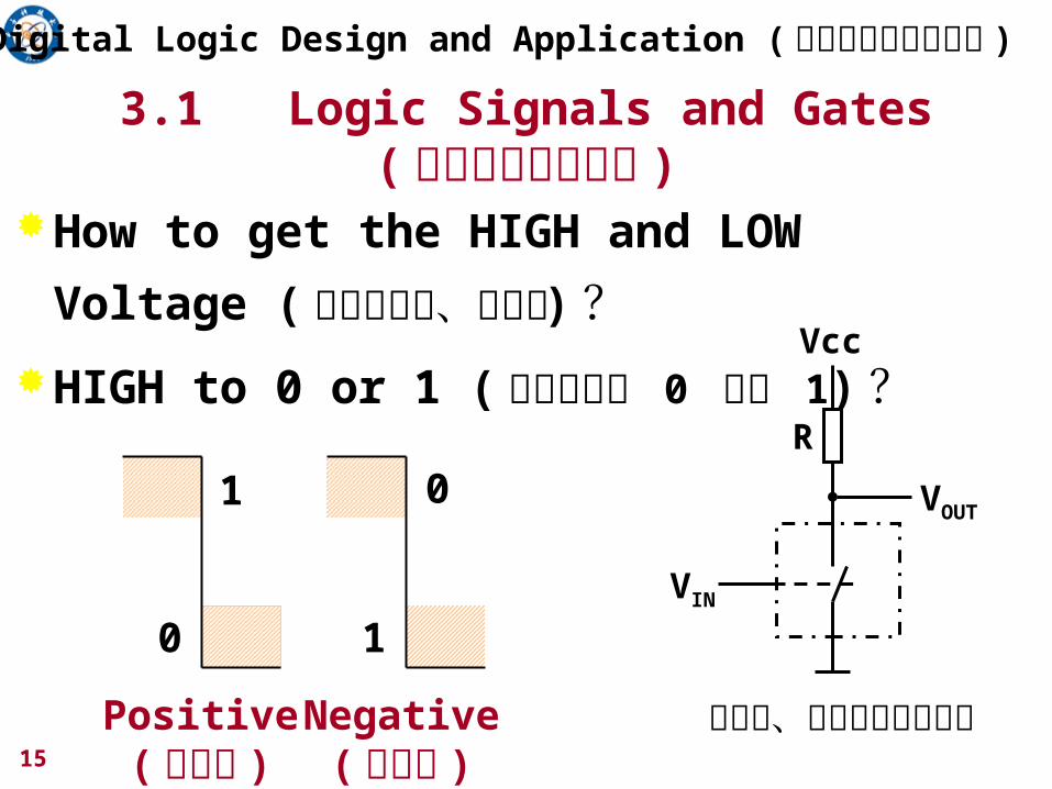
3.1 Logic Signals and Gates(逻辑信号和门电路 )
How to get the HIGH and LOW Voltage
(如何获得高、低电平 )?
HIGH to 0 or 1 ( 高电平对应 0 还是 1)?
VOUT
VIN
Vcc
R
获得高、低电平的基本原理Positive( 正逻辑 )
1
0
Negative( 负逻辑 )
1
0
1616
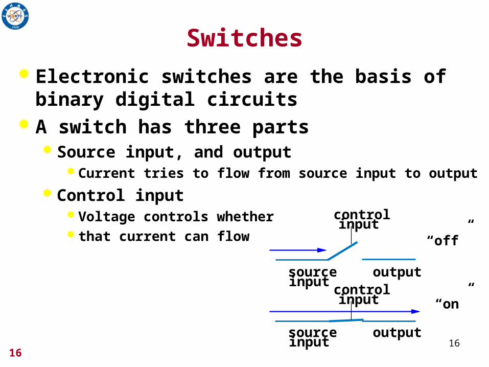
Switches Electronic switches are the basis of binary digital
circuits A switch has three parts
Source input, and output Current tries to flow from source input to output
Control input Voltage controls whether that current can flow “off”
“on”
outputsourceinput
outputsourceinput
controlinput
controlinput
17 17
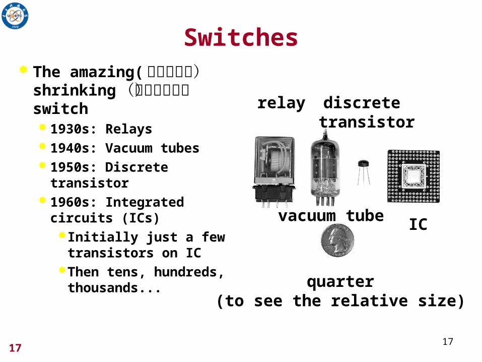
Switches The amazing(令人惊奇
的) shrinking(逐渐减 小的) switch
1930s: Relays 1940s: Vacuum tubes 1950s: Discrete
transistor 1960s: Integrated circuits
(ICs)Initially just a few
transistors on ICThen tens, hundreds,
thousands...
relay
vacuum tube
discrete transistor
IC
quarter(to see the relative size)
1818
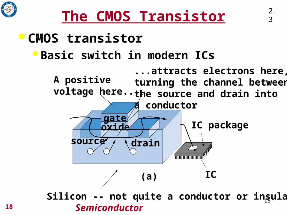
The CMOS TransistorCMOS transistor
Basic switch in modern ICs
Silicon -- not quite a conductor or insulator:Semiconductor
2.3
gate
source drain
oxide
A positive voltage here...
(a)
IC package
IC
...attracts electrons here, turning the channel betweenthe source and drain intoa conductor
1919
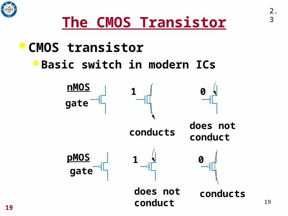
The CMOS Transistor
CMOS transistorBasic switch in modern ICs
does notconduct
0
conducts
1gate
nMOS
does notconduct
1gatepMOS
conducts
0
2.3
2020
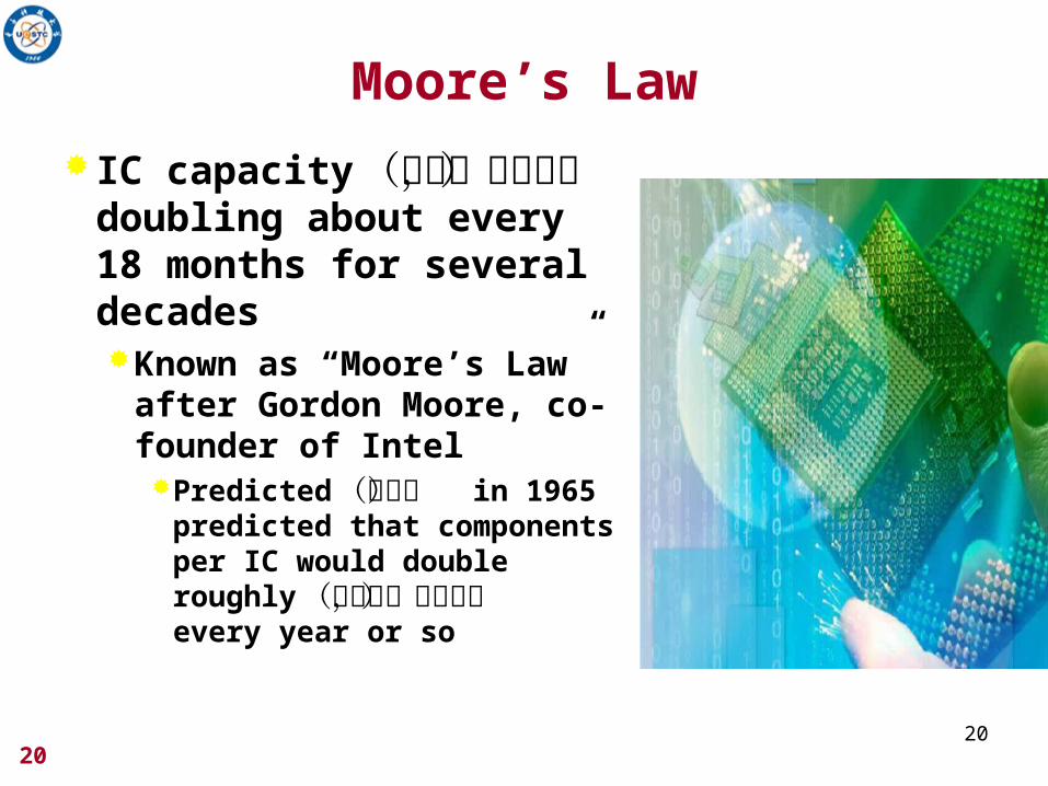
Moore’s Law
IC capacity(容量,集成 度) doubling about every
18 months for several decadesKnown as “Moore’s Law”
after Gordon Moore, co-founder of IntelPredicted (预言) in 1965
predicted that components per IC would double roughly(粗
略地,大致上) every year or so
21
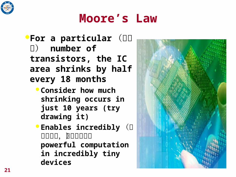
Moore’s Law
For a particular(特定 的) number of
transistors, the IC area shrinks by half every 18 months
Consider how much shrinking occurs in just 10 years (try drawing it)
Enables incredibly(不 能相信的,难以置信的)
powerful computation in incredibly tiny devices
22
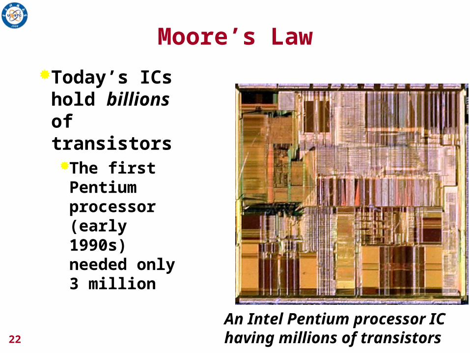
Moore’s Law
Today’s ICs hold billions of transistorsThe first
Pentium processor (early 1990s) needed only 3 million
An Intel Pentium processor IChaving millions of transistors
23
3.1 Logic Signals and Gates(逻辑信号和门电路 )
Digital Logic Design and Application ( 数字逻辑设计及应用 )
从物理的角度考虑电路如何工作,工作中的电气特性实际物理器件不可避免的时间延迟问题
从逻辑角度输入、输出的逻辑关系
三种基本逻辑:与、或、非
2424
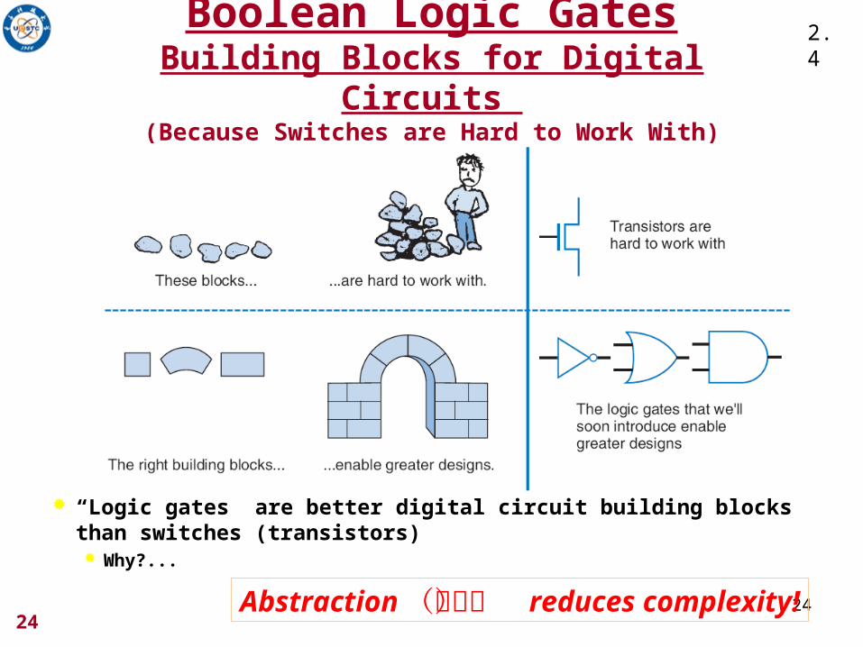
Boolean Logic GatesBuilding Blocks for Digital Circuits
(Because Switches are Hard to Work With)
“Logic gates” are better digital circuit building blocks than switches (transistors) Why?...
2.4
Abstraction (提取) reduces complexity!
2525
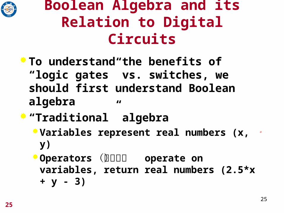
Boolean Algebra and its Relation to Digital Circuits
To understand the benefits of “logic gates” vs. switches, we should first understand Boolean algebra
“Traditional” algebraVariables represent real numbers (x, y)Operators (运算器) operate on
variables, return real numbers (2.5*x + y - 3)
a
2626
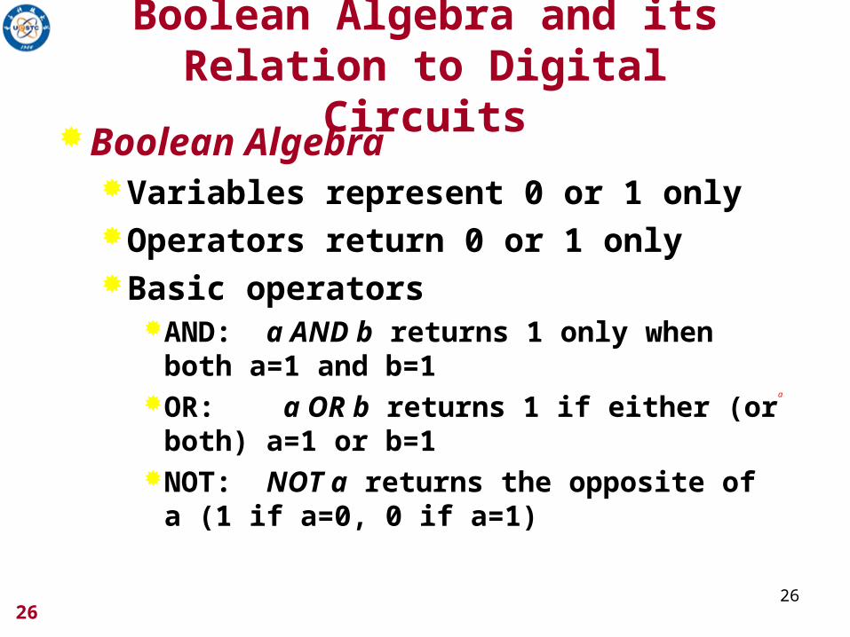
Boolean Algebra and its Relation to Digital Circuits
Boolean AlgebraVariables represent 0 or 1 onlyOperators return 0 or 1 onlyBasic operators
AND: a AND b returns 1 only when both a=1 and b=1
OR: a OR b returns 1 if either (or both) a=1 or b=1
NOT: NOT a returns the opposite of a (1 if a=0, 0 if a=1)
a
27
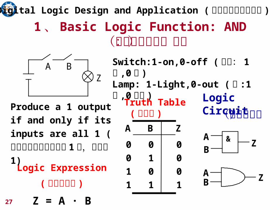
1、 Basic Logic Function: AND(基本逻辑运算:与)
0 0 00 1 01 0 01 1 1
A BZ
Logic Expression
( 逻辑表达式 )
Z = A · B
Switch:1-on,0-off ( 开关: 1通 ,0断 )Lamp: 1-Light,0-out (灯 :1亮 ,0 不亮 )
Produce a 1 output if
and only if its inputs
are all 1 ( 当且仅当所有输入全为 1 时,输出为 1)
Truth Table ( 真值表 )
&AB
Z
AB Z
(逻辑符号)A B Z
Logic Circuit
Digital Logic Design and Application ( 数字逻辑设计及应用 )
28
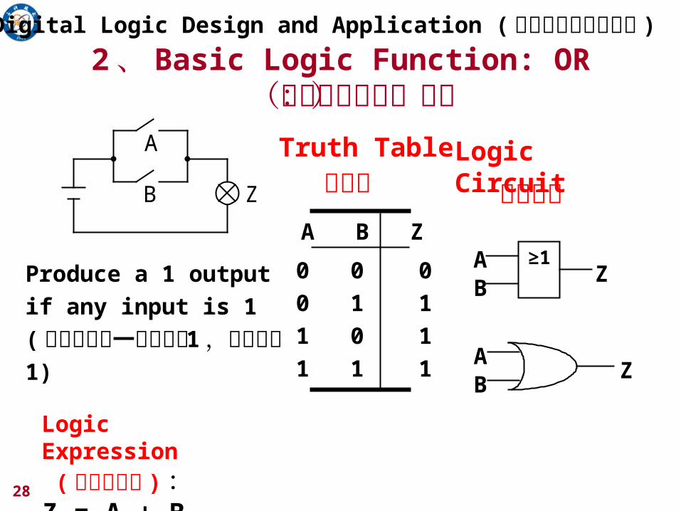
2、 Basic Logic Function: OR(基本逻辑运算:或)
Logic Expression ( 逻辑表达式 ) :Z = A + B
A B Z
真值表A
B Z
Produce a 1 output if
any input is 1
( 只要有任何一个输入为 1
,输出就为 1)
≥1AB
Z
AB
Z
逻辑符号
0 0 00 1 11 0 11 1 1
Truth Table Logic Circuit
Digital Logic Design and Application ( 数字逻辑设计及应用 )
29
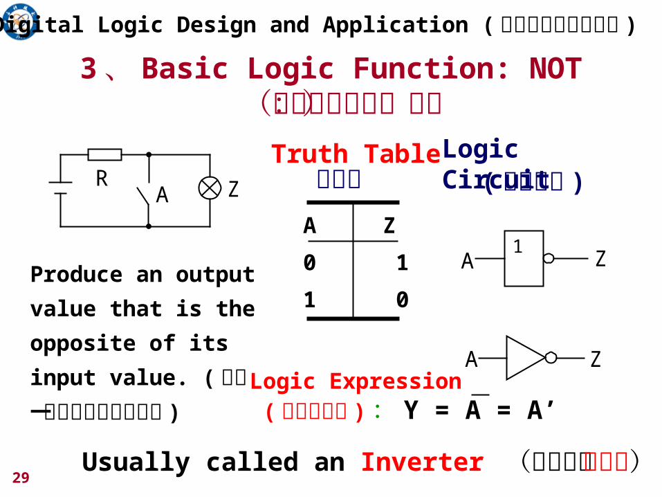
A Z
0 1
1 0
真值表
Logic Expression ( 逻辑表达式 ): Y = A = A’
A ZR
Produce an
output value that
is the opposite of
its input value. (
产生一个与输入相反的输出 )
Usually called an Inverter (通常称为反相器)
1ZA
A Z
( 逻辑符号 )
Digital Logic Design and Application ( 数字逻辑设计及应用 )
3、 Basic Logic Function: NOT(基本逻辑运算:非)
Truth Table Logic Circuit
30
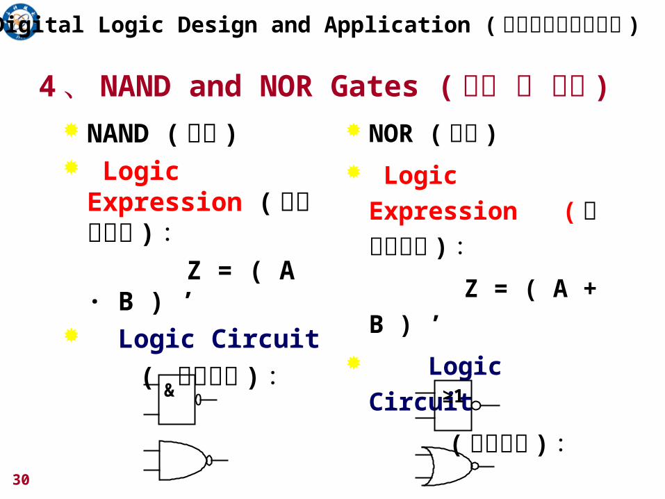
4、 NAND and NOR Gates ( 与非 和 或非 )
NAND (与非 ) Logic Expression
(逻辑表达式 ): Z = ( A · B ) ’ Logic Circuit
( 逻辑符号 ):
NOR (或非 )
Logic Expression
(逻辑表达式 ):
Z = ( A + B ) ’
Logic Circuit
(逻辑符号 ):
& ≥1
Digital Logic Design and Application ( 数字逻辑设计及应用 )
31
Digital Logic Design and Application ( 数字逻辑设计及应用 )
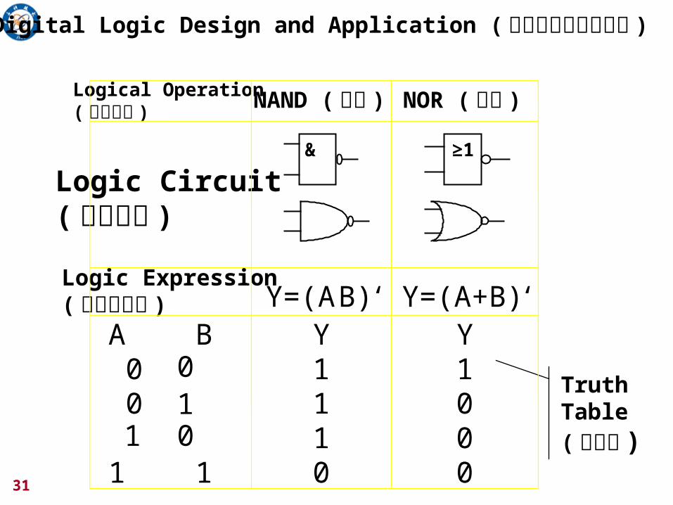
Truth Table ( 真值表 )
& ≥1
Logical Operation( 逻辑运算 ) NAND ( 与非 ) NOR ( 或非 )
Logic Circuit( 逻辑符号 )
Logic Expression( 逻辑表达式 )
Y=(AžB)’‘
Y=(A+B)’‘A B 0 0 1 1 1
Y 1 1 1 0
Y 1 0 0 0
10
0
3232
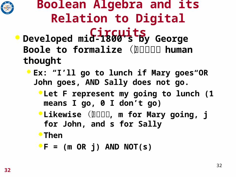
Boolean Algebra and its Relation to Digital Circuits
Developed mid-1800’s by George Boole to formalize(使成正式) human thought Ex: “I’ll go to lunch if Mary goes OR John goes,
AND Sally does not go.”Let F represent my going to lunch (1 means I
go, 0 I don’t go)Likewise(类似地) , m for Mary going, j for
John, and s for SallyThen F = (m OR j) AND NOT(s)
3333
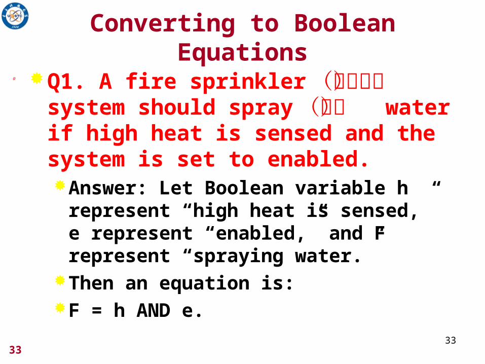
Converting to Boolean Equations
Q1. A fire sprinkler (洒水器) system should spray (喷) water if high heat is sensed and the system is set to enabled.Answer: Let Boolean variable h represent
“high heat is sensed,” e represent “enabled,” and F represent “spraying water.”
Then an equation is: F = h AND e.
a
3434
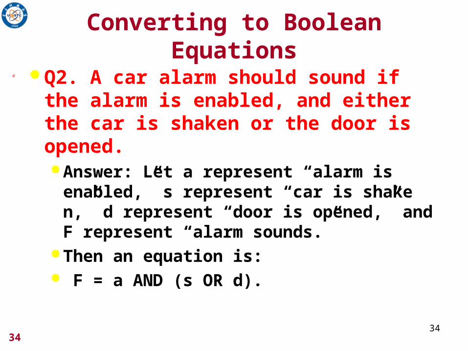
Converting to Boolean Equations
Q2. A car alarm should sound if the alarm is enabled, and either the car is shaken or the door is opened. Answer: Let a represent “alarm is enable
d,” s represent “car is shaken,” d represent “door is opened,” and F represent “alarm sounds.”
Then an equation is: F = a AND (s OR d).
a
35
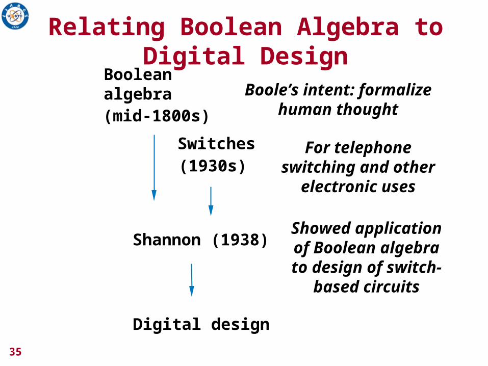
Relating Boolean Algebra to Digital Design
Booleanalgebra(mid-1800s)
Boole’s intent: formalizehuman thought
Switches(1930s)
Shannon (1938)
Digital design
Showed applicationof Boolean algebrato design of switch-
based circuits
For telephoneswitching and other
electronic uses
36
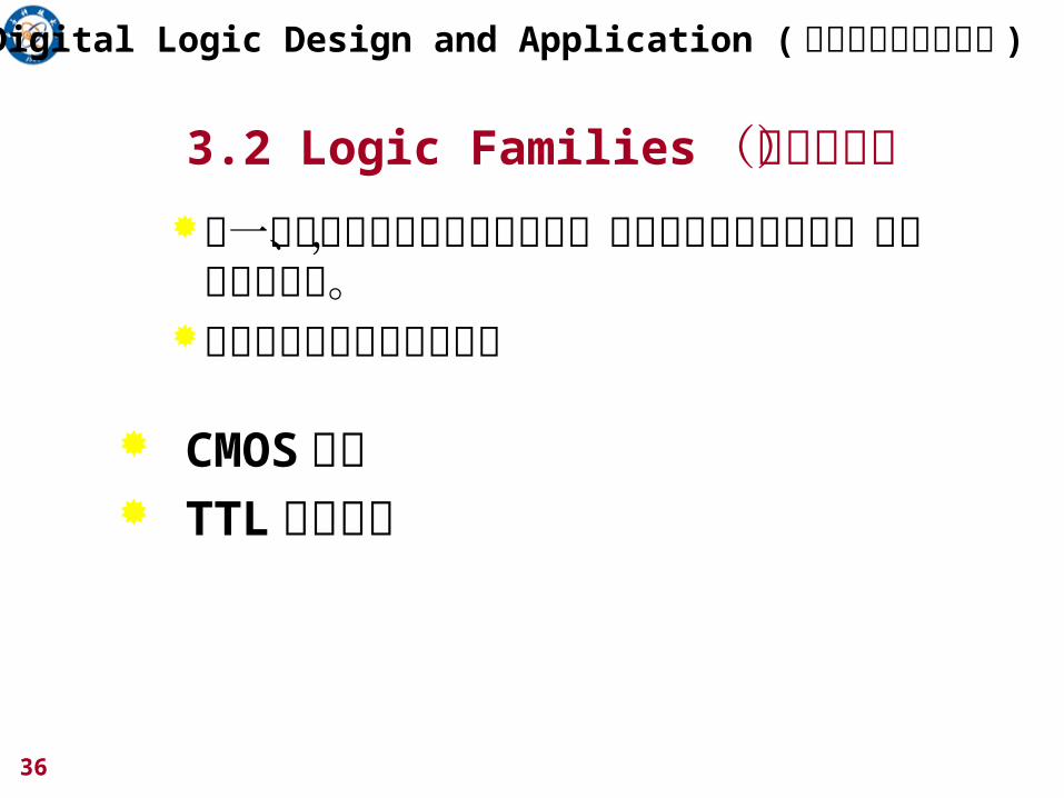
Digital Logic Design and Application ( 数字逻辑设计及应用 )
3.2 Logic Families(逻辑系列)同一系列的芯片具有类似的输入、输出及内部电路特征,但逻辑功能不同。
不同系列的芯片可能不匹配
CMOS系列 TTL逻辑系列
37
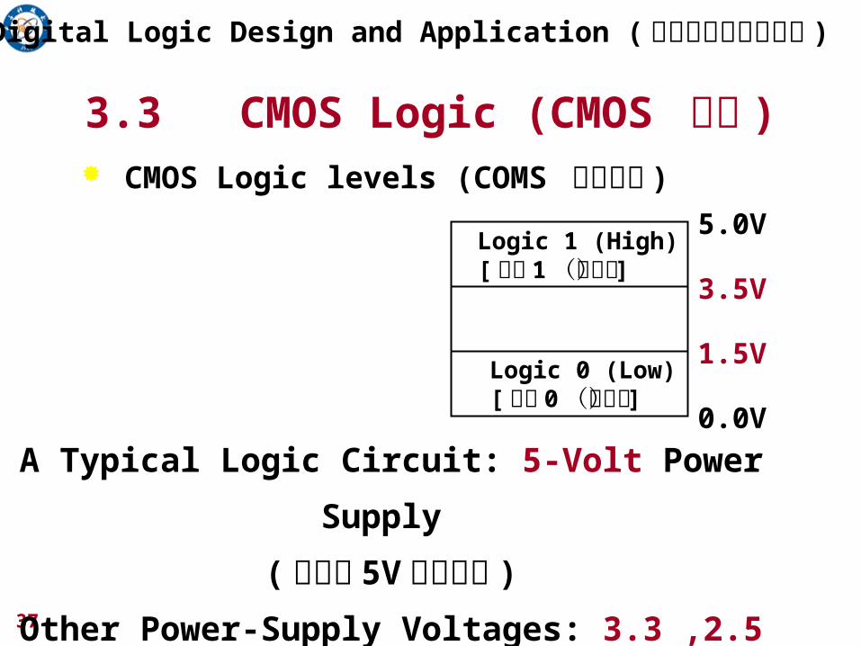
Digital Logic Design and Application ( 数字逻辑设计及应用 )
3.3 CMOS Logic (CMOS 逻辑 ) CMOS Logic levels (COMS 逻辑电平 )
5.0V
3.5V
1.5V
0.0V
A Typical Logic Circuit: 5-Volt Power Supply
( 典型的 5V 电源电压 )
Other Power-Supply Voltages: 3.3 ,2.5 or 1.8Volts
( 其它电源电压: 3.3V ,2.5V或 1.8V)
Logic 1 (High)[ 逻辑 1 (高态) ]
Logic 0 (Low)[ 逻辑 0 (低态) ]
38
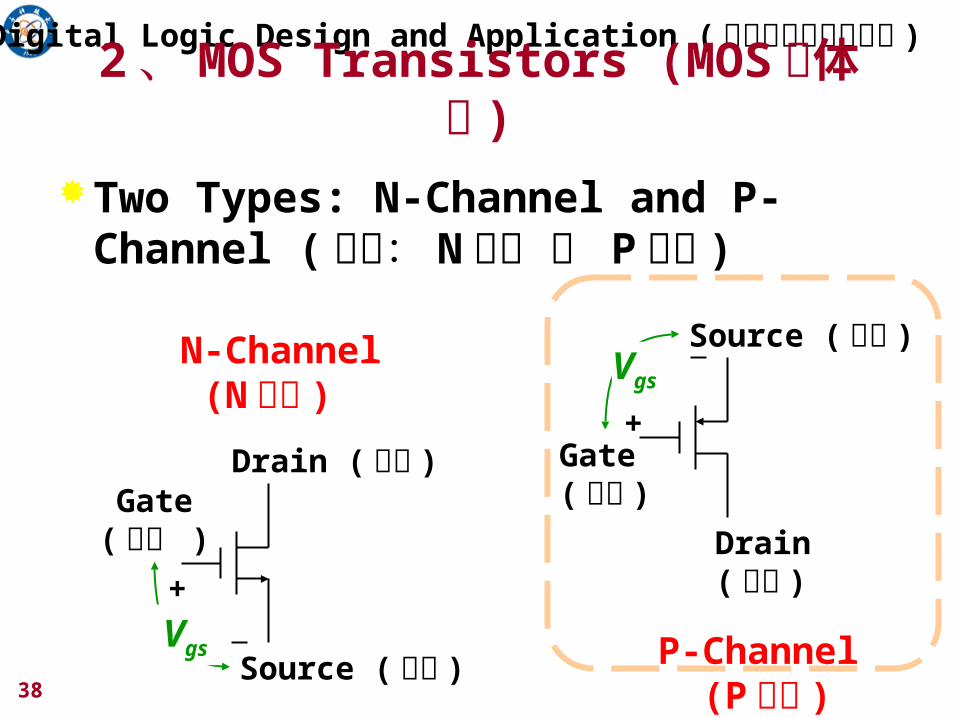
Digital Logic Design and Application ( 数字逻辑设计及应用 )2、MOS Transistors (MOS晶体
管 )Two Types: N-Channel and P-Channel
(分为: N 沟道 和 P沟道 )
Drain ( 漏极 )
Source ( 源极 )
Gate( 栅极 )
Vgs
+
N-Channel (N 沟道 )
Source ( 源极 )
Drain( 漏极 )
Gate( 栅极 )
+
Vgs
P-Channel (P 沟道 )
39
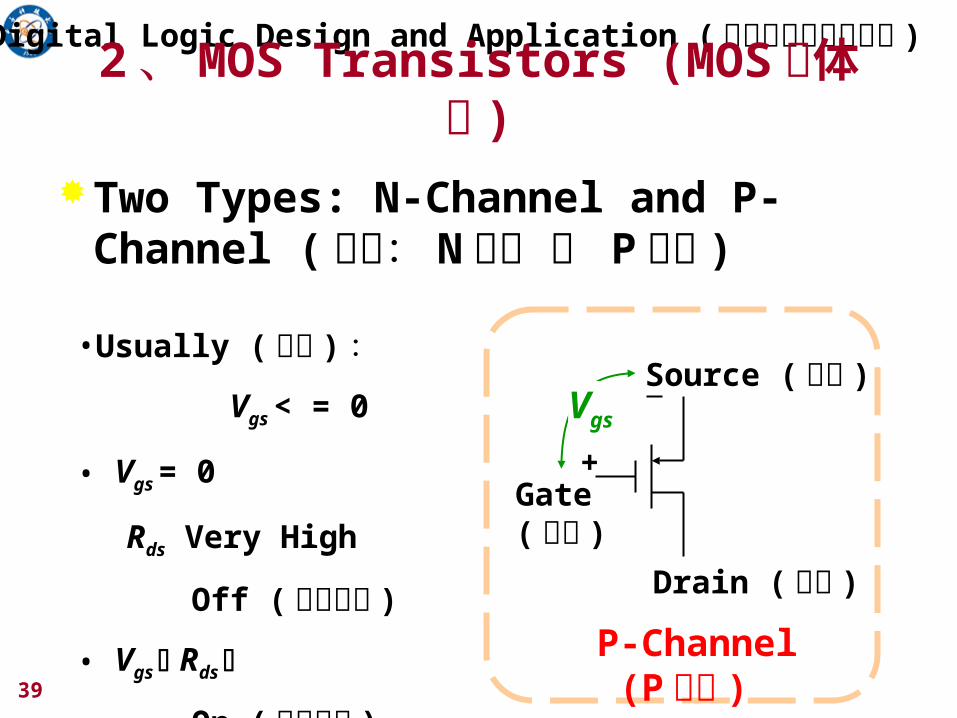
Digital Logic Design and Application ( 数字逻辑设计及应用 )2、MOS Transistors (MOS晶体
管 )Two Types: N-Channel and P-Channel
(分为: N 沟道 和 P沟道 )
Source ( 源极 )
Drain ( 漏极 )
Gate( 栅极 )
+
Vgs
P-Channel (P 沟道 )
•Usually ( 通常 ) :
Vgs < = 0
• Vgs = 0
Rds Very High
Off ( 截止状态 )
• Vgs Rds
On ( 导通状态 )
40
Digital Logic Design and Application ( 数字逻辑设计及应用 )
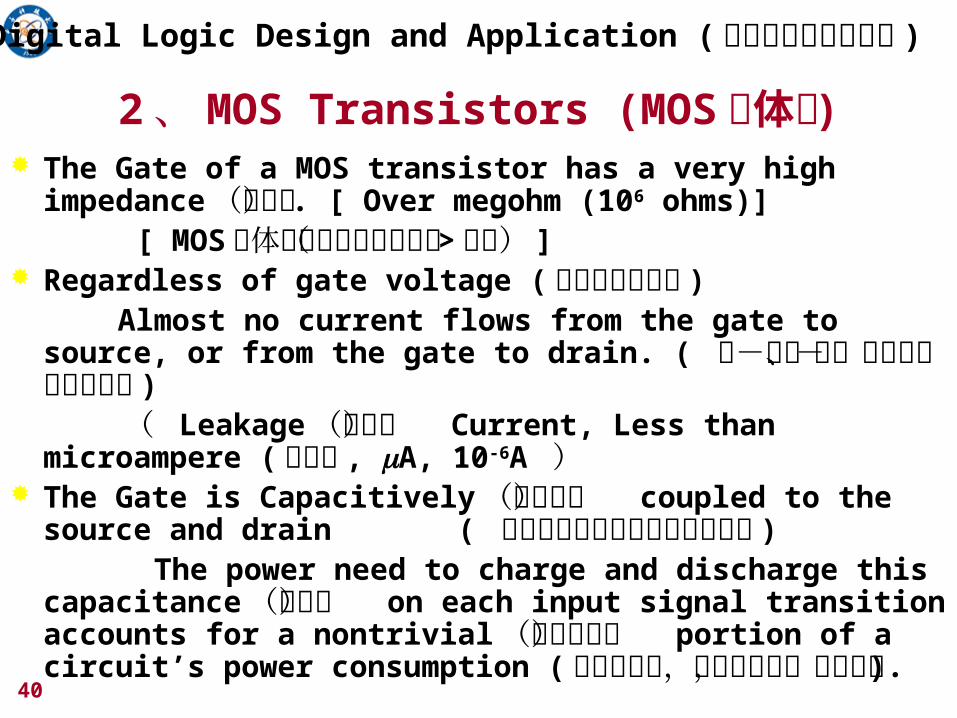
2、MOS Transistors (MOS晶体管 ) The Gate of a MOS transistor has a very high
impedance(阻抗) . [ Over megohm (106 ohms)] [ MOS晶体管栅极阻抗非常高( >兆欧) ] Regardless of gate voltage (无论栅电压如何 ) Almost no current flows from the gate to source, or from
the gate to drain. ( 栅-源、栅-漏之间几乎没有电流 ) ( Leakage (漏出) Current, Less than
microampere (漏电流 , A, 10-6A ) The Gate is Capacitively (容性地) coupled to the source
and drain ( 栅极与源和漏极之间有容性耦合 ) The power need to charge and discharge this
capacitance (电容) on each input signal transition accounts for a nontrivial (非平凡的) portion of a circuit’s power consumption (信号转换时,电容充放电,功耗较大 ).
41
Digital Logic Design and Application ( 数字逻辑设计及应用 )
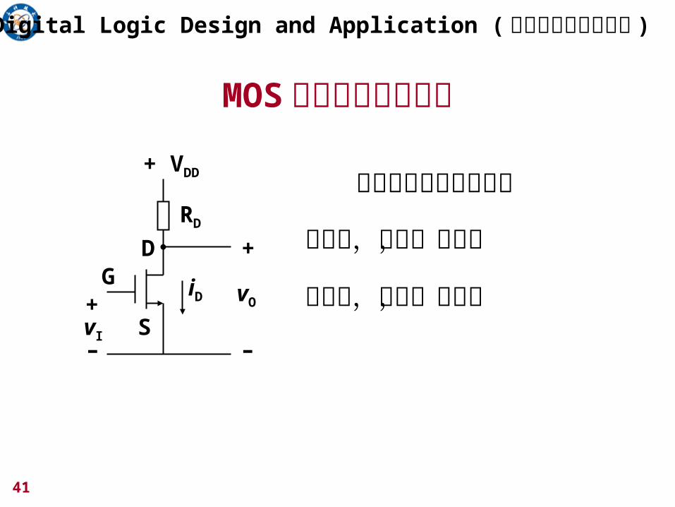
MOS管的基本开关电路
vI
+
–
vO
–
+
iD
+ VDD
RD
DG
S
只要电路参数选择合理
输入低,截止,输出高
输入高,导通,输出低
42
Digital Logic Design and Application ( 数字逻辑设计及应用 )
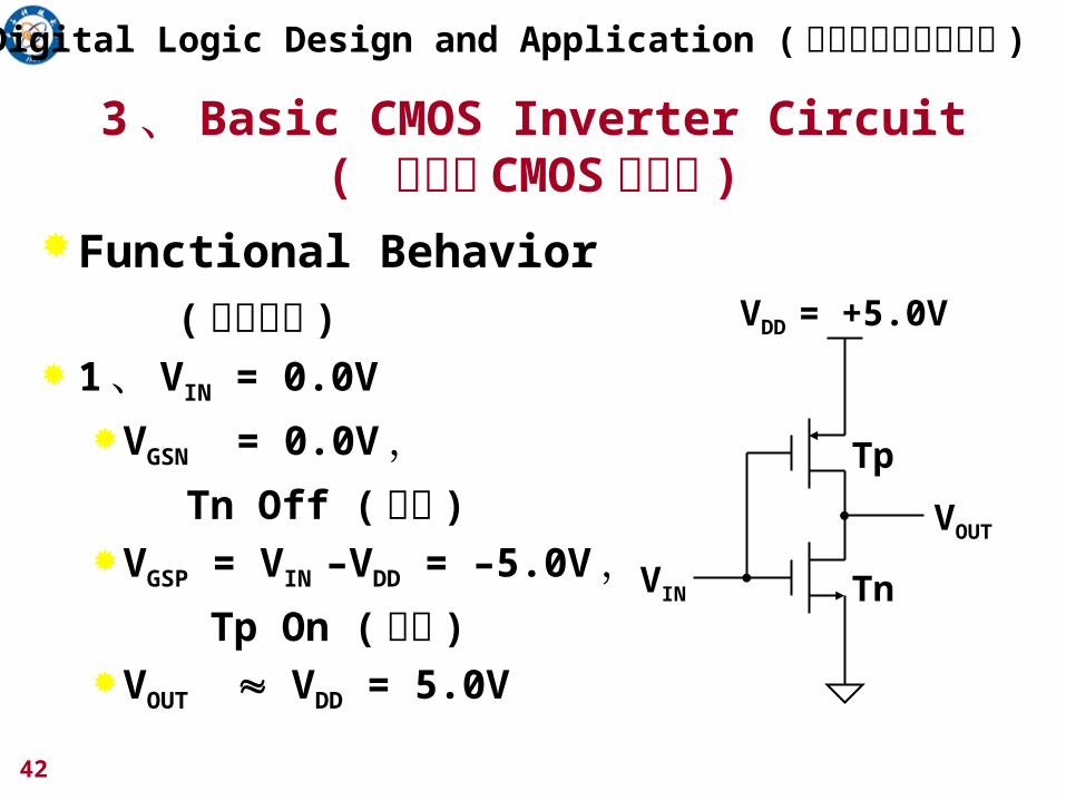
3、 Basic CMOS Inverter Circuit( 基本的 CMOS反相器 )
Functional Behavior
(工作原理 ) 1、 VIN = 0.0V
VGSN = 0.0V,
Tn Off (截止 )VGSP = VIN –VDD = –5.0V,
Tp On (导通 )VOUT VDD = 5.0V
VDD = +5.0V
VOUT
VIN
Tp
Tn
43
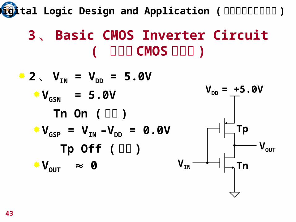
3、 Basic CMOS Inverter Circuit( 基本的 CMOS反相器 )
2、 VIN = VDD = 5.0V
VGSN = 5.0V
Tn On (导通 )VGSP = VIN –VDD = 0.0V
Tp Off (截止 )VOUT 0
VDD = +5.0V
VOUT
VIN
Tp
Tn
Digital Logic Design and Application ( 数字逻辑设计及应用 )
4444
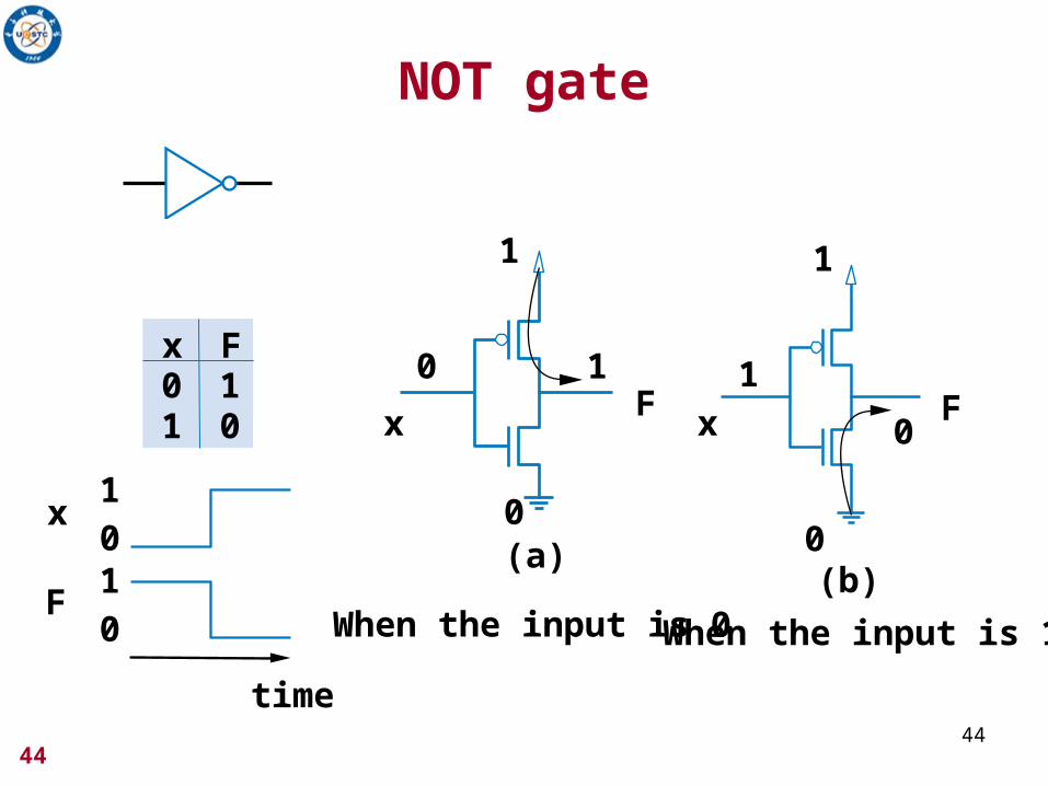
NOT gate
x01
F10
1
0
F1
x
0
(a)
1
0
F0x
1
(b)When the input is 0 When the input is 1
01
1
0
time
F
x
45
Digital Logic Design and Application ( 数字逻辑设计及应用 )
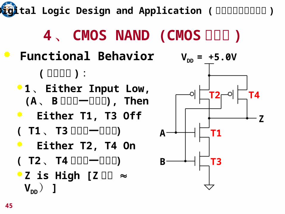
4、 CMOS NAND (CMOS与非门 ) Functional Behavior
(工作原理 ) :1、 Either Input Low,
(A、 B至少有一个为低 ), Then
Either T1, T3 Off
( T1、 T3至少有一个截止 ) Either T2, T4 On
( T2、 T4至少有一个导通 )Z is High [Z 为高 VDD) ]
VDD = +5.0V
Z
A
B
T1
T2 T4
T3
46
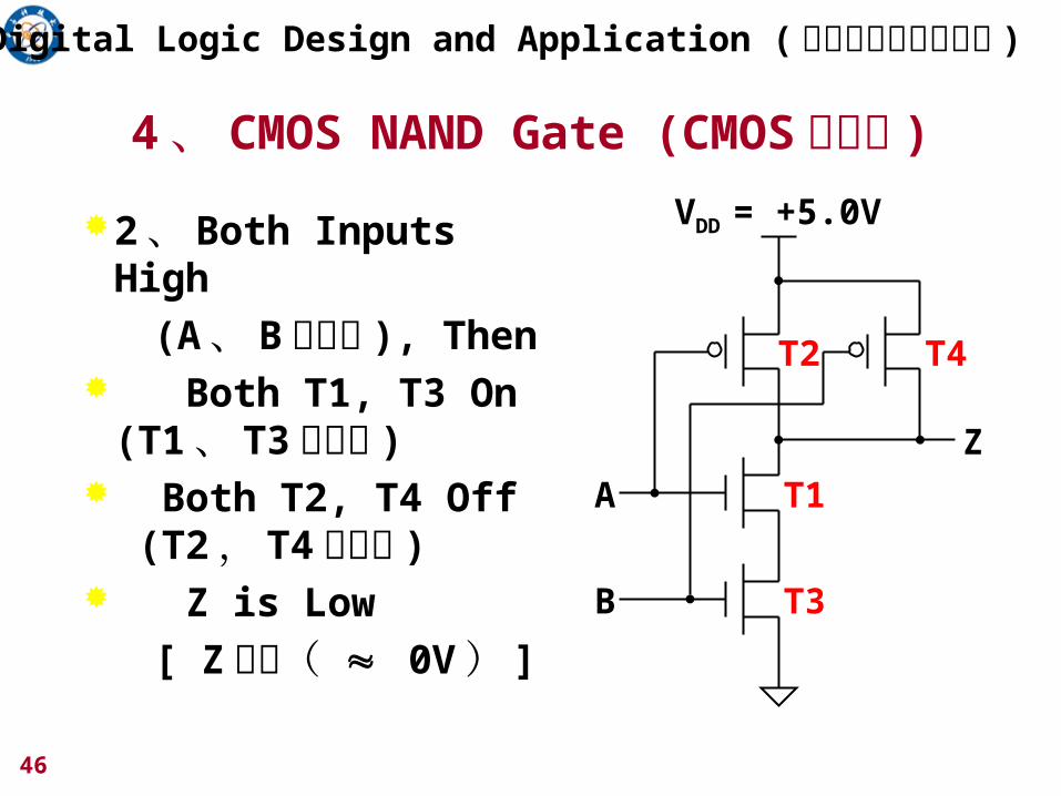
4、 CMOS NAND Gate (CMOS与非门 )
2、 Both Inputs High
(A、 B都为高 ), Then Both T1, T3 On
(T1、 T3都导通 ) Both T2, T4 Off
(T2, T4都截止 ) Z is Low
[ Z 为低( 0V) ]
VDD = +5.0V
Z
A
B
T1
T2 T4
T3
Digital Logic Design and Application ( 数字逻辑设计及应用 )
47
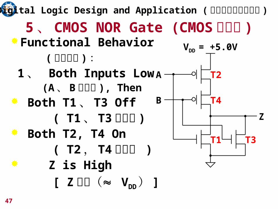
5、 CMOS NOR Gate (CMOS或非门 )
Functional Behavior (工作原理 ): 1 、 Both Inputs Low
(A、 B都为低 ), Then Both T1、 T3 Off ( T1、 T3都截止 ) Both T2, T4 On ( T2, T4 都导通 ) Z is High
[ Z为高( VDD) ]
VDD = +5.0V
Z
A
B
T1
T2
T4
T3
Digital Logic Design and Application ( 数字逻辑设计及应用 )
48
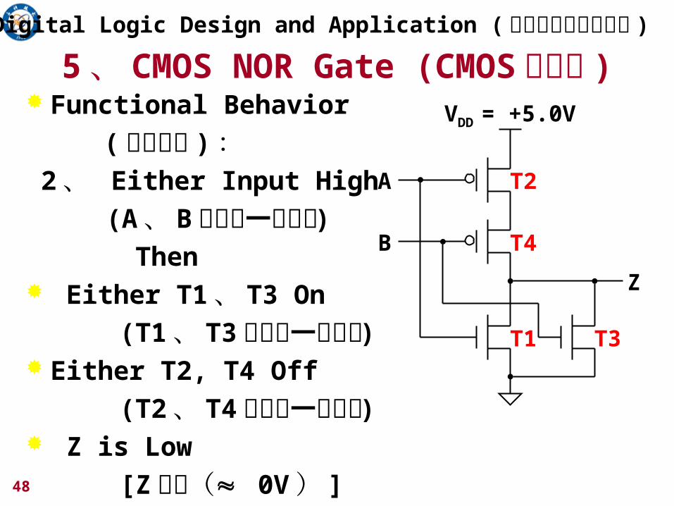
5、 CMOS NOR Gate (CMOS或非门 )
Functional Behavior
(工作原理 ): 2 、 Either Input High
(A、 B至少有一个为高 )
Then Either T1、 T3 On
(T1、 T3至少有一个导通 ) Either T2, T4 Off
(T2、 T4至少有一个截止 ) Z is Low
[Z为低( 0V) ]
VDD = +5.0V
Z
A
B
T1
T2
T4
T3
Digital Logic Design and Application ( 数字逻辑设计及应用 )
4949
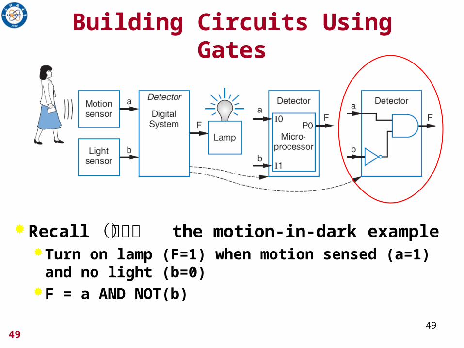
Building Circuits Using Gates
Recall (回想) the motion-in-dark exampleTurn on lamp (F=1) when motion sensed (a=1)
and no light (b=0)F = a AND NOT(b)
5050
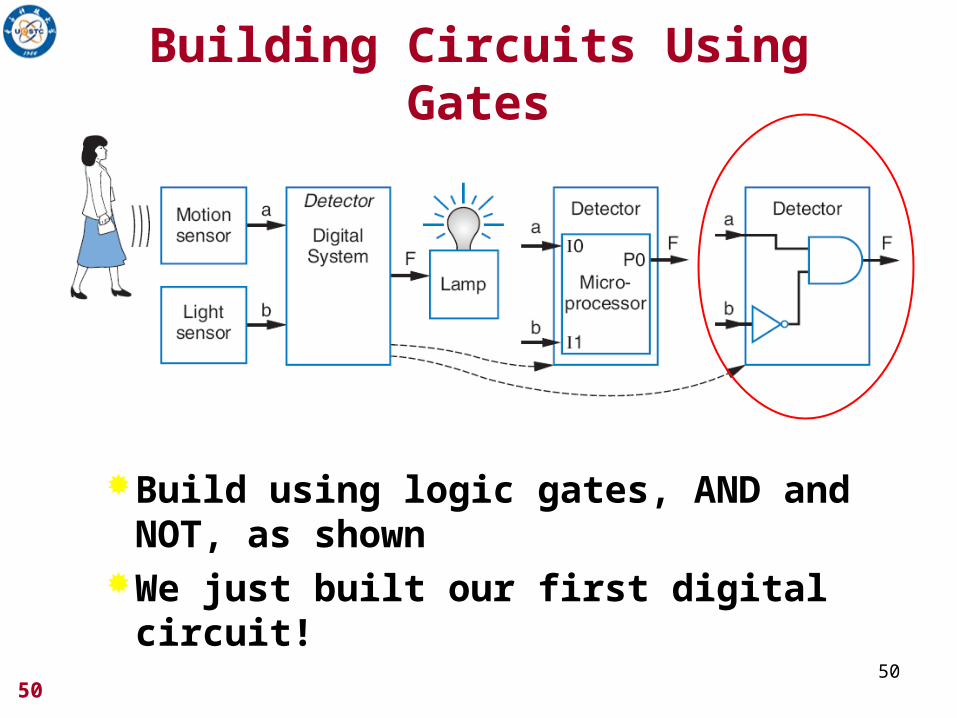
Building Circuits Using Gates
Build using logic gates, AND and NOT, as shown
We just built our first digital circuit!
5151
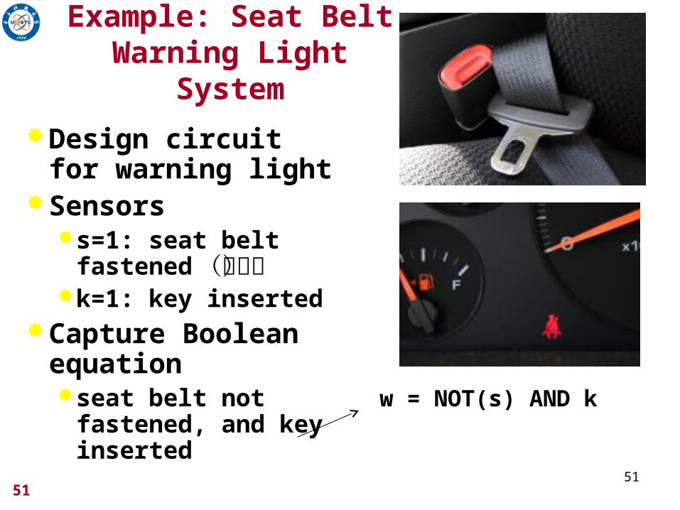
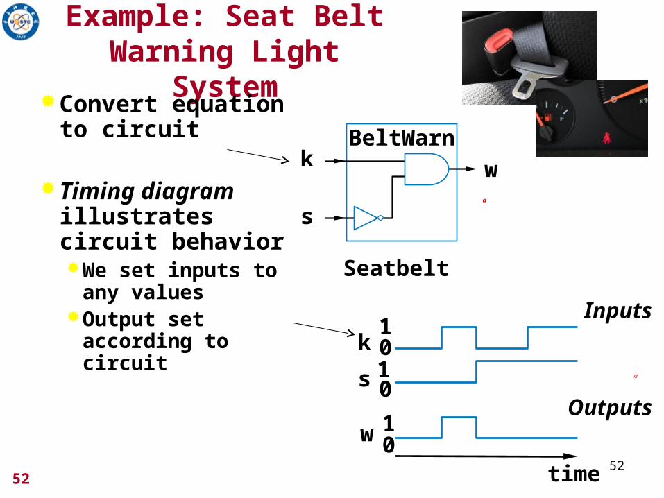
Example: Seat Belt Warning Light
System
Design circuit for warning light
Sensorss=1: seat belt
fastened(系紧)k=1: key inserted
Capture Boolean equationseat belt not
fastened, and key inserted
w = NOT(s) AND k
5252
Example: Seat Belt Warning Light
SystemConvert equation to circuit
Timing diagram illustrates circuit behaviorWe set inputs to any
valuesOutput set
according to circuit
a
a
time
Inputs
Outputs
1
1
1
0
0
0
k
s
w
k
s
w
BeltWarn
Seatbelt
5353
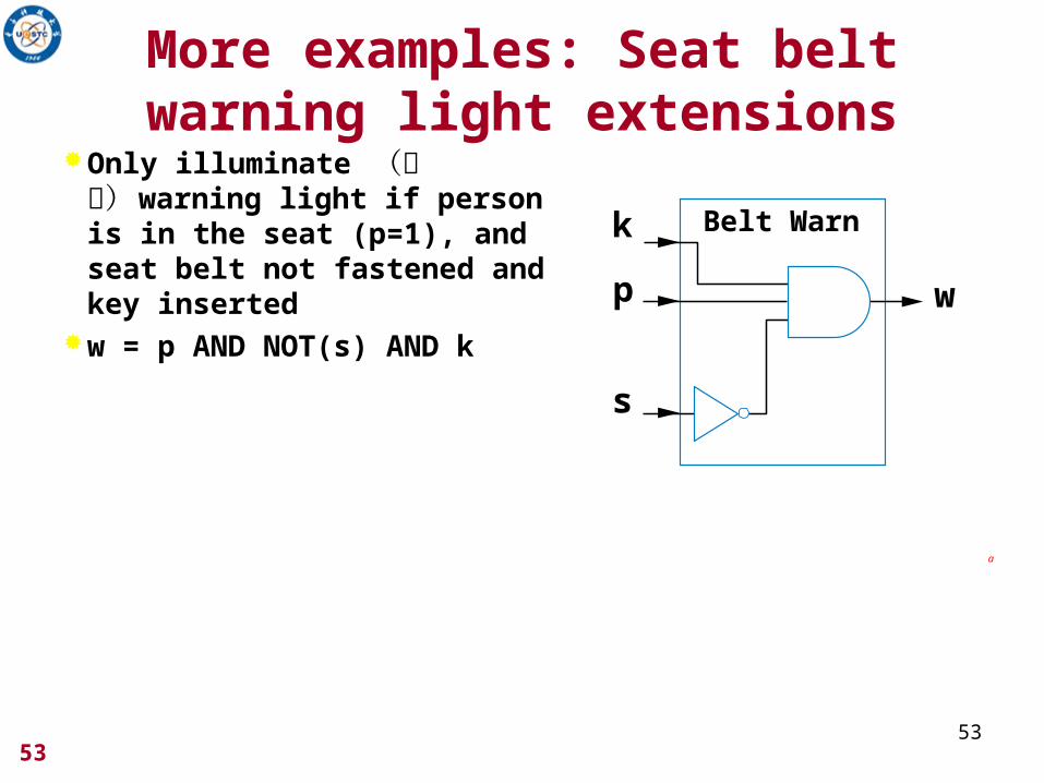
More examples: Seat belt warning light extensions
Only illuminate (照亮)warning light if person is in the seat (p=1), and seat belt not fastened and key inserted
w = p AND NOT(s) AND k
k
p
s
w
Belt Warn
a
5454
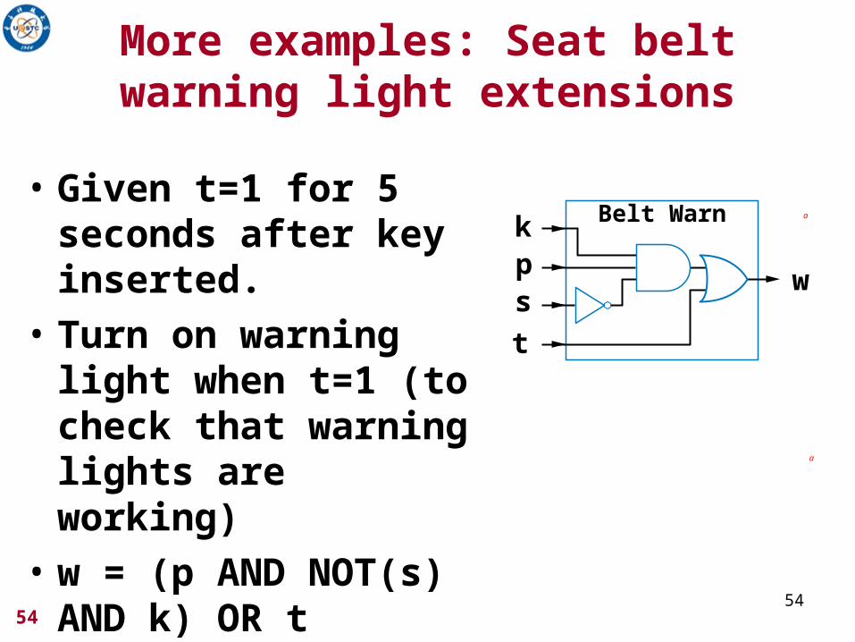
More examples: Seat belt warning light extensions
a
• Given t=1 for 5 seconds after key inserted.
• Turn on warning light when t=1 (to check that warning lights are working)
• w = (p AND NOT(s) AND k) OR t
a
k
wps
t
Belt Warn
55
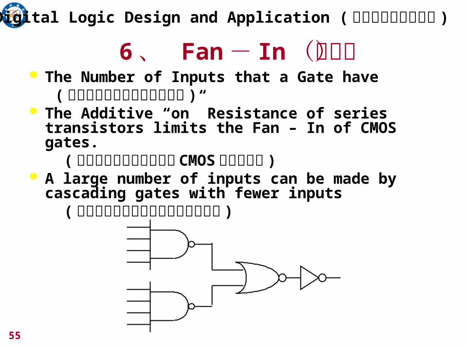
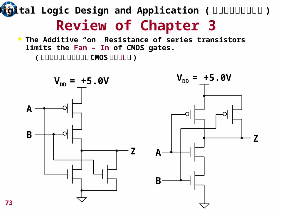
6 、 Fan- In(扇入) The Number of Inputs that a Gate have (门电路所具有的输入端的数目 ) The Additive “on” Resistance of series transistors
limits the Fan – In of CMOS gates. (导通电阻的可加性限制了 CMOS门的扇入数 ) A large number of inputs can be made by cascading
gates with fewer inputs (可用较少输入门级联得到较多的输入 )
Digital Logic Design and Application ( 数字逻辑设计及应用 )
56
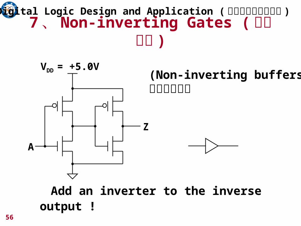
7、 Non-inverting Gates (非反相门 )
VDD = +5.0V
A
Z
(Non-inverting buffers)非反相缓冲器
Digital Logic Design and Application ( 数字逻辑设计及应用 )
Add an inverter to the inverse output !
57
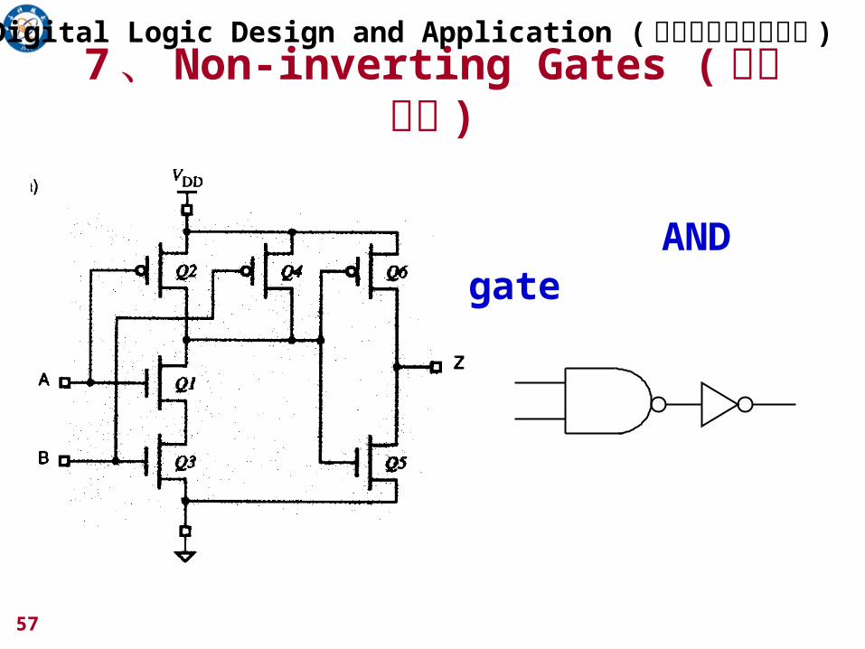
7、 Non-inverting Gates (非反相门 )
Digital Logic Design and Application ( 数字逻辑设计及应用 )
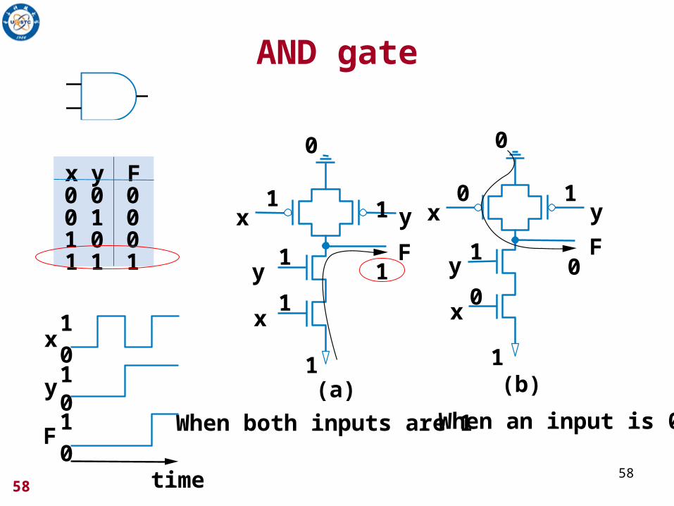
AND gate
5858
AND gate
x0011
y0101
F0001
0
1 1
11
1
1
y
y
F
x
x
(a)
0
0 1
01
0
1
y
y
F
x
x
(b)
When both inputs are 1 When an input is 0
1
0x
y
F1
1
0
0
time
5959
OR gate
x0011
y0101
F0111
0
1
0
0 1
1
1
y
x
x
y
F
(a)
0
0
0
0 0
0
1
y
x
x
y
F
(b)When an input is 1 When both inputs are 0
10x
y
F1
1
0
0
time
60
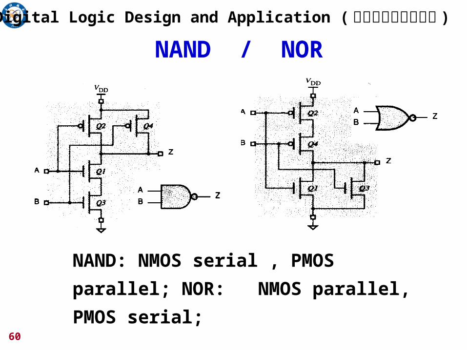
Digital Logic Design and Application ( 数字逻辑设计及应用 )
NAND / NOR
NAND: NMOS serial , PMOS parallel;
NOR: NMOS parallel, PMOS serial;
61
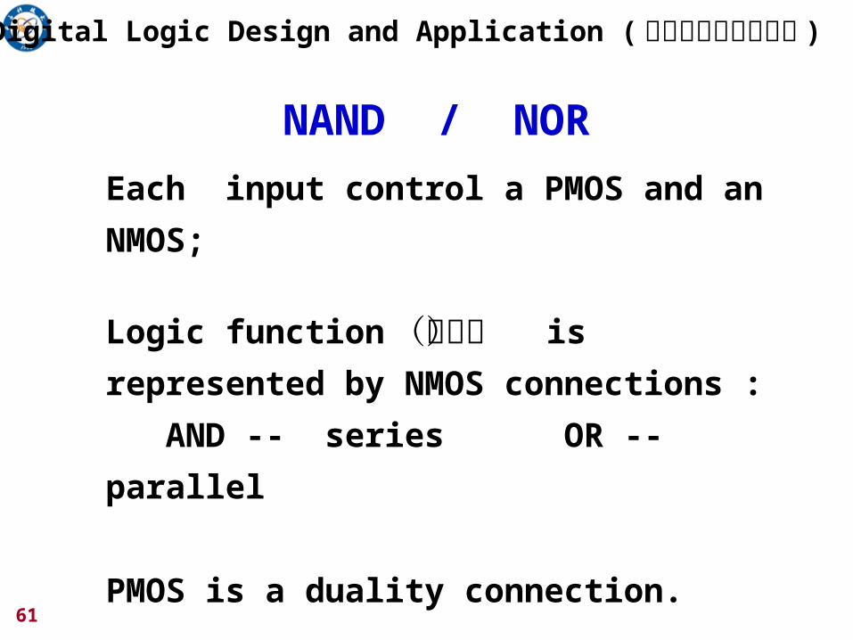
Digital Logic Design and Application ( 数字逻辑设计及应用 )
Each input control a PMOS and an NMOS;
Logic function (功能) is represented by
NMOS connections :
AND -- series OR -- parallel
PMOS is a duality connection.
NAND / NOR
62
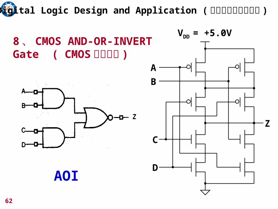
VDD = +5.0V
A
B
Z
C
D
8、 CMOS AND-OR-INVERT Gate ( CMOS 与或非门 )
Digital Logic Design and Application ( 数字逻辑设计及应用 )
AOI
63
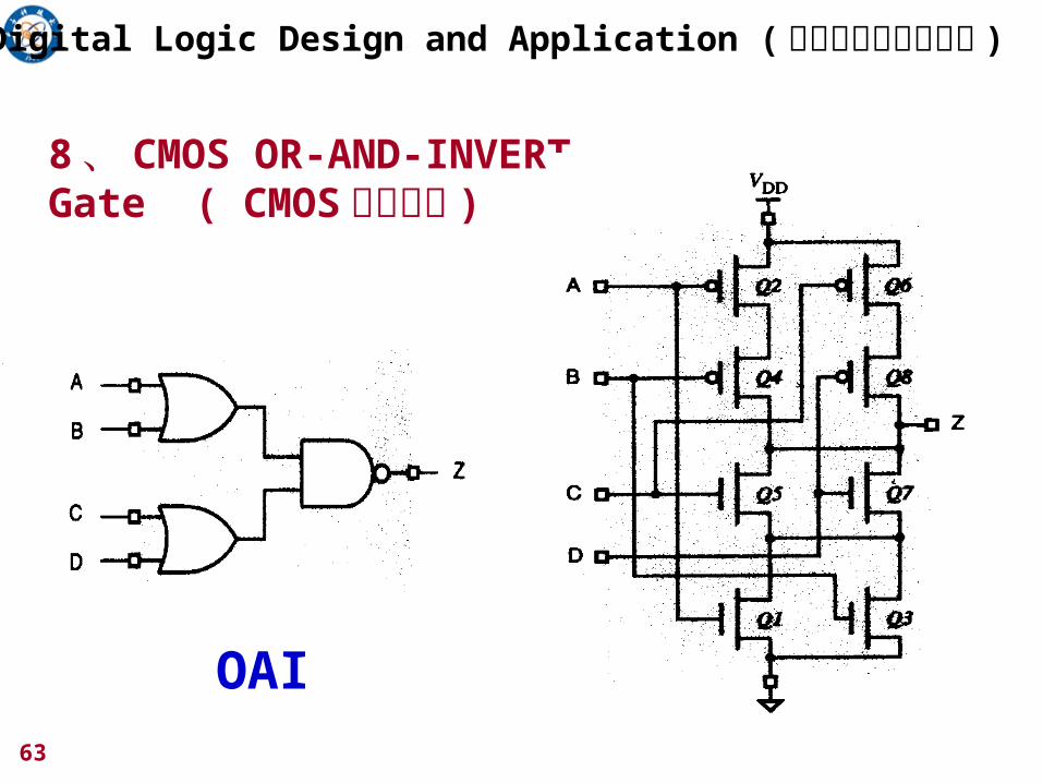
8、 CMOS OR-AND-INVERT Gate ( CMOS 或与非门 )
Digital Logic Design and Application ( 数字逻辑设计及应用 )
OAI
64
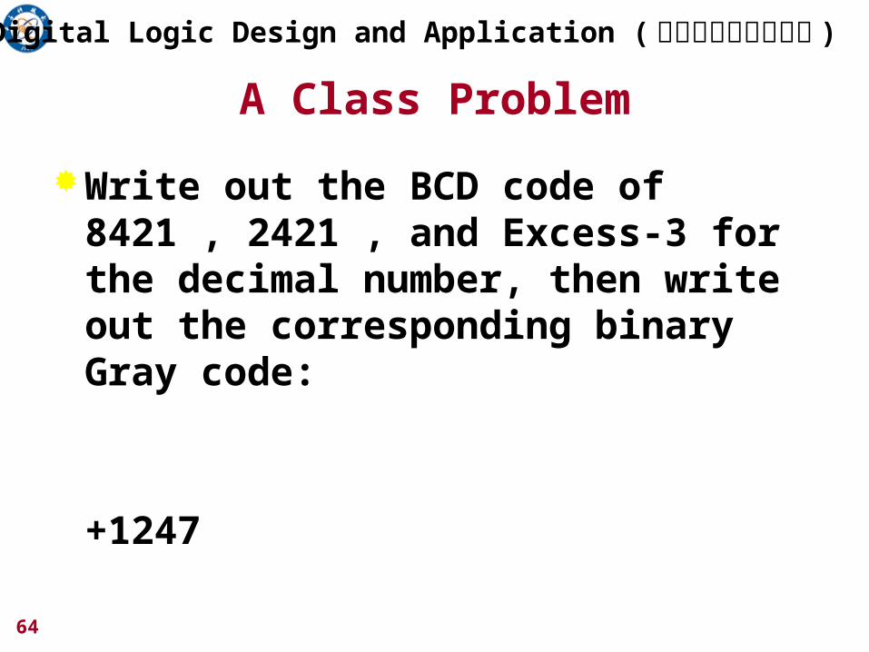
A Class Problem
Write out the BCD code of 8421 , 2421 , and Excess-3 for the decimal number, then write out the corresponding binary Gray code:
+1247
Digital Logic Design and Application ( 数字逻辑设计及应用 )
65
Chapter 3 Digital Circuits
(数字电路 )
Give a knowledge of the Electrical aspects of Digital Circuits
(介绍数字电路中的电气知识 )
Digital Logic Design and Application ( 数字逻辑设计及应用 )
66
Digital Logic Design and Application ( 数字逻辑设计及应用 )
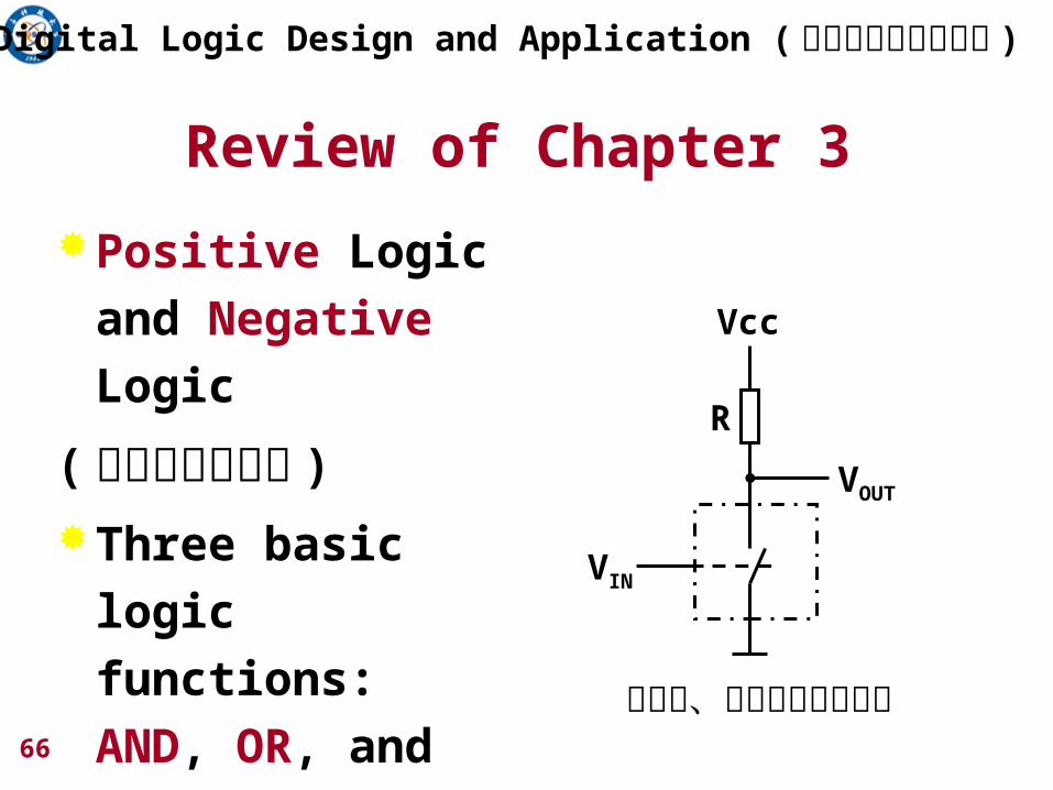
Review of Chapter 3
Positive Logic and
Negative Logic
(正逻辑和负逻辑 )
Three basic logic
functions: AND,
OR, and NOT
(三种基本逻辑:与、或、非 )
VOUT
VIN
Vcc
R
获得高、低电平的基本原理
67
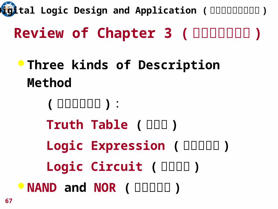
Review of Chapter 3 (第三章内容回顾 )
Digital Logic Design and Application ( 数字逻辑设计及应用 )
Three kinds of Description Method
(三种描述方法 ):
Truth Table (真值表 )
Logic Expression (逻辑表达式 )
Logic Circuit (逻辑符号 )
NAND and NOR (与非和或非 )
68
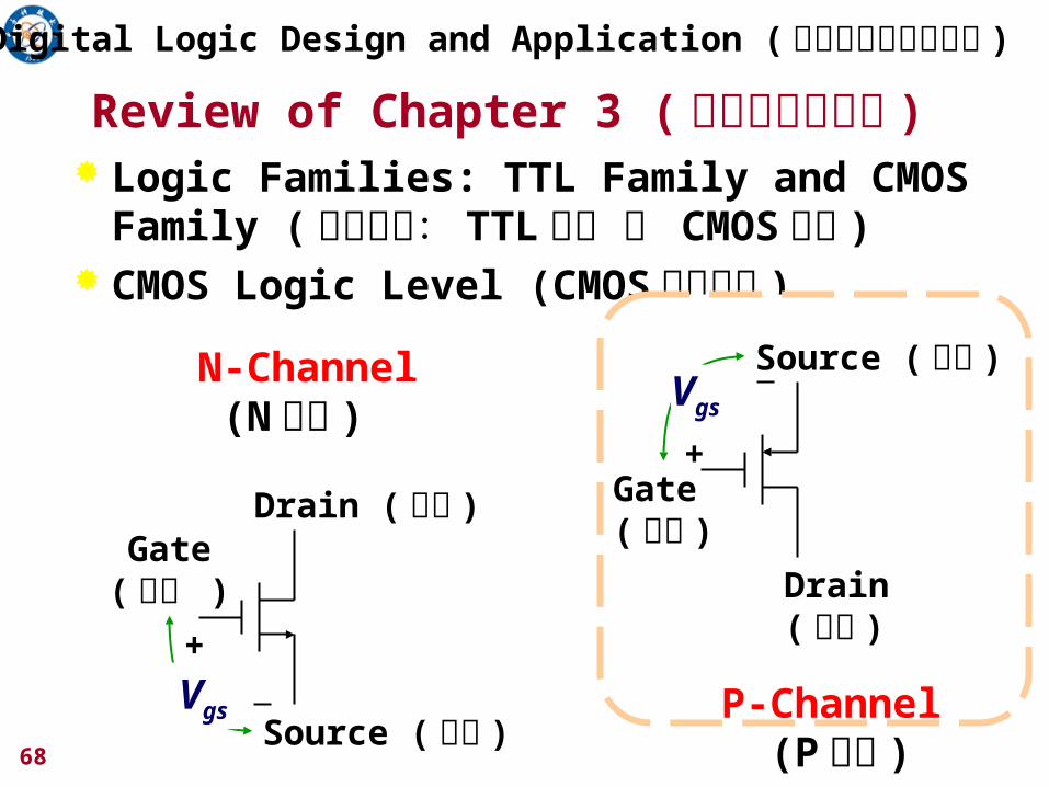
Review of Chapter 3 (第三章内容回顾 )
Digital Logic Design and Application ( 数字逻辑设计及应用 )
Logic Families: TTL Family and CMOS Family (逻辑系列: TTL 系列 和 CMOS系列 )
CMOS Logic Level (CMOS逻辑电平 )
Drain ( 漏极 )
Source ( 源极 )
Gate( 栅极 )
Vgs
+
Source ( 源极 )
Drain( 漏极 )
Gate( 栅极 )
+
Vgs
P-Channel (P 沟道 )
N-Channel (N 沟道 )
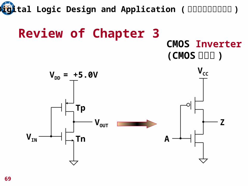
69
VDD = +5.0V
VOUT
VIN
Tp
Tn
VCC
A
Z
CMOS Inverter (CMOS 反相器 )
Digital Logic Design and Application ( 数字逻辑设计及应用 )
Review of Chapter 3
70
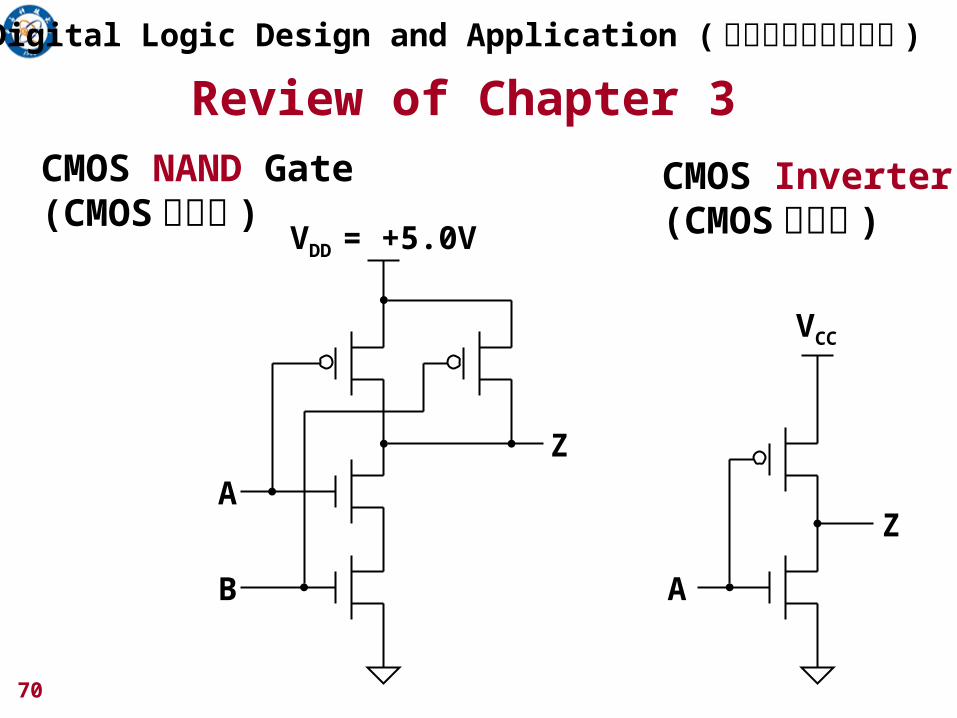
VCC
A
Z
CMOS Inverter(CMOS 反相器 )VDD = +5.0V
Z
A
B
CMOS NAND Gate(CMOS 与非门 )
Review of Chapter 3Digital Logic Design and Application ( 数字逻辑设计及应用 )
71
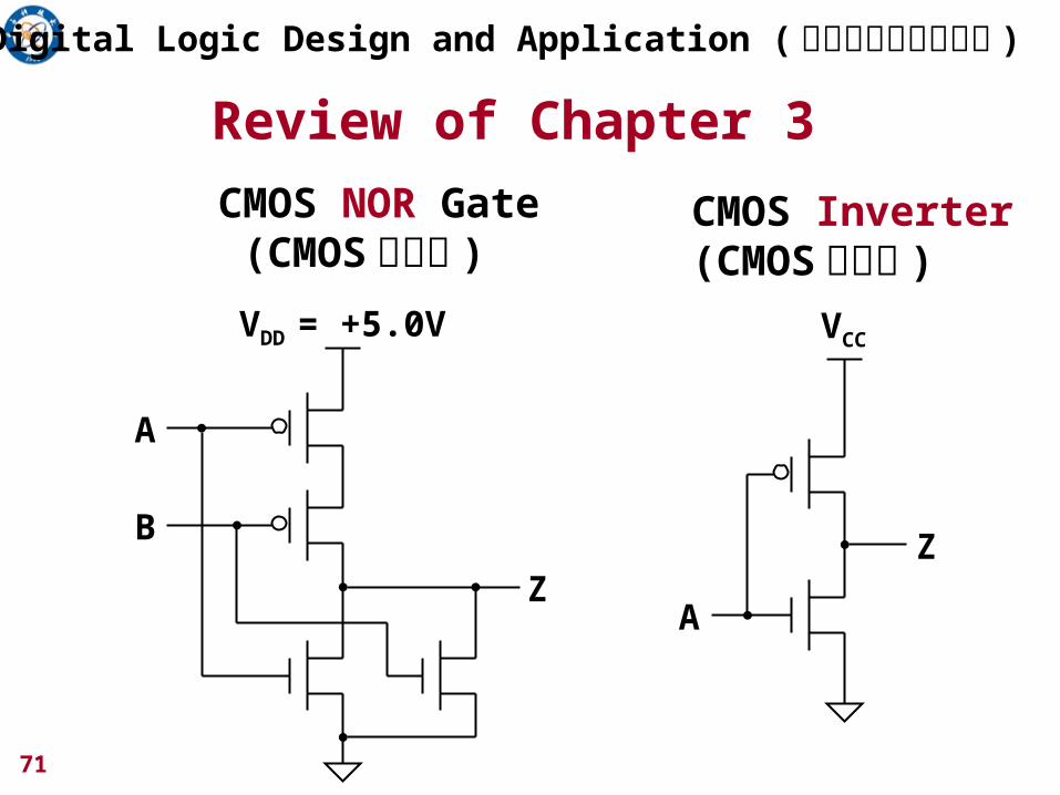
VCC
A
Z
CMOS Inverter(CMOS 反相器 )
VDD = +5.0V
Z
A
B
CMOS NOR Gate (CMOS 或非门 )
Review of Chapter 3
Digital Logic Design and Application ( 数字逻辑设计及应用 )
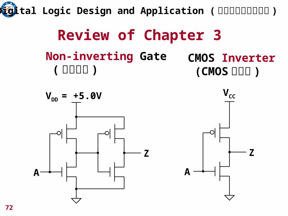
72
VCC
A
Z
CMOS Inverter (CMOS 反相器 )
VDD = +5.0V
A
Z
Non-inverting Gate ( 非反相门 )
Review of Chapter 3
Digital Logic Design and Application ( 数字逻辑设计及应用 )
73
The Additive “on” Resistance of series transistors limits the Fan – In of CMOS gates.
(导通电阻的可加性限制了CMOS门的扇入数 )
VDD = +5.0V
Z
A
B
VDD = +5.0V
Z
A
B
Review of Chapter 3Digital Logic Design and Application ( 数字逻辑设计及应用 )
74
Digital Logic Design and Application ( 数字逻辑设计及应用 )
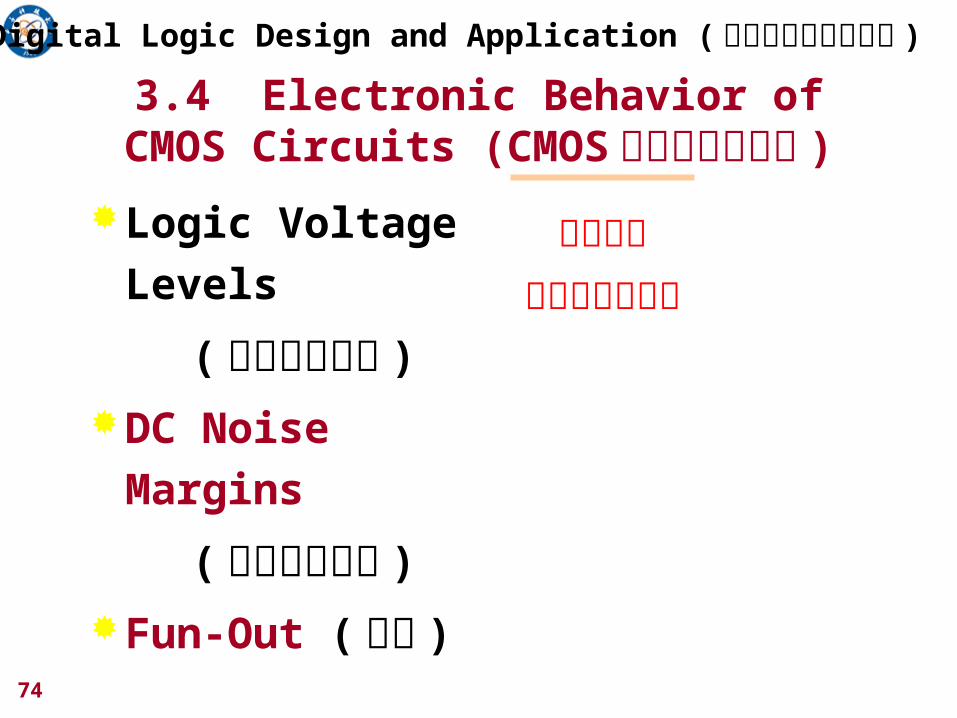
3.4 Electronic Behavior of CMOS Circuits (CMOS电路的电气特性 )
Logic Voltage
Levels
(逻辑电压电平 )
DC Noise
Margins
(直流噪声容限 )
Fun-Out (扇出 )
物理上的而不是逻辑上的
75
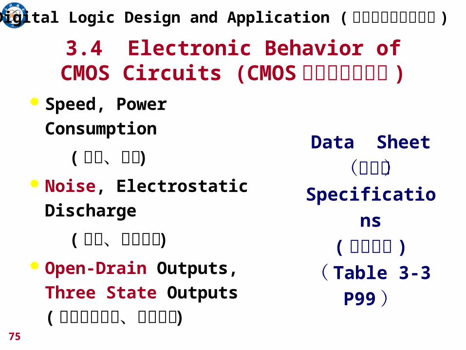
3.4 Electronic Behavior of CMOS Circuits (CMOS电路的电气特性 )
Speed, Power
Consumption
(速度、功耗 )
Noise, Electrostatic
Discharge
(噪声、静电放电 )
Open-Drain Outputs,
Three State Outputs (漏极开路输出、三态输出 )
Data Sheet(数据表)
Specifications
( 规格说明 )( Table 3-3
P99)
Digital Logic Design and Application ( 数字逻辑设计及应用 )
76
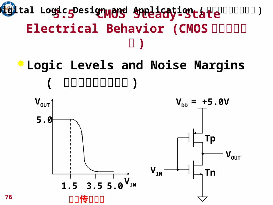
3.5 CMOS Steady-State Electrical Behavior (CMOS稳态电
气特性 )
Logic Levels and Noise Margins
( 逻辑电平和噪声容限 )
VDD = +5.0V
VOUT
VIN
Tp
Tn
VOUT
VIN5.01.5 3.5
5.0
电压传输特性
Digital Logic Design and Application ( 数字逻辑设计及应用 )
77
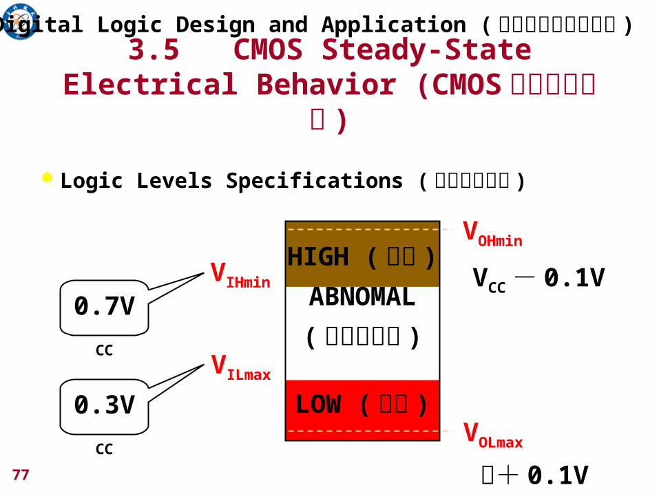
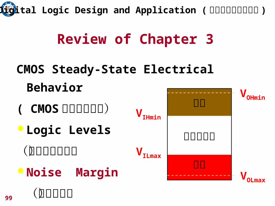
Logic Levels Specifications (逻辑电平规格 )
HIGH ( 高态 )
ABNOMAL
( 不正常状态 )
LOW ( 低态 )VOLmax
VILmax
VIHmin
VOHmin
VCC- 0.1V
地+ 0.1V
0.7VCC
0.3VCC
Digital Logic Design and Application ( 数字逻辑设计及应用 )3.5 CMOS Steady-State
Electrical Behavior (CMOS稳态电气特性 )
78
Digital Logic Design and Application ( 数字逻辑设计及应用 )
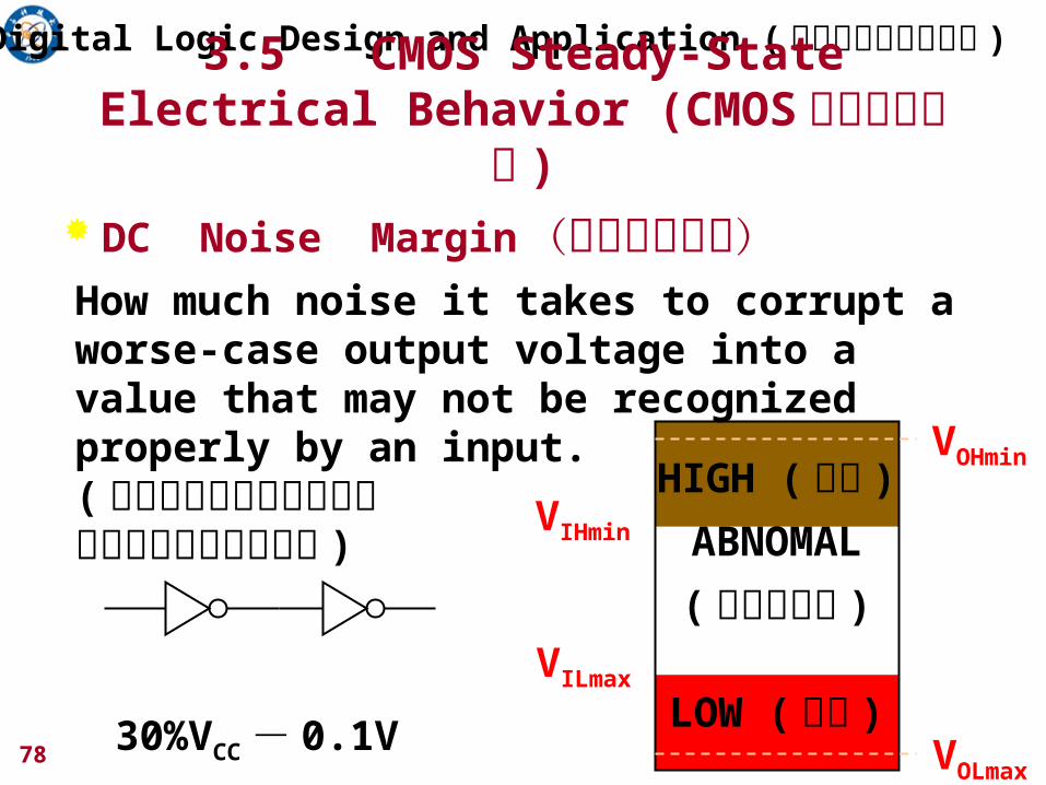
DC Noise Margin (直流噪声容限)
HIGH ( 高态 )
ABNOMAL
( 不正常状态 )
LOW ( 低态 )VOLmax
VILmax
VIHmin
VOHmin
30%VCC- 0.1V
3.5 CMOS Steady-State Electrical Behavior (CMOS稳态电
气特性 )
How much noise it takes to corrupt a worse-case output voltage into a value that may not be recognized properly by an input.( 多大的噪声会使最坏输出电压被破坏得不可识别 )
79
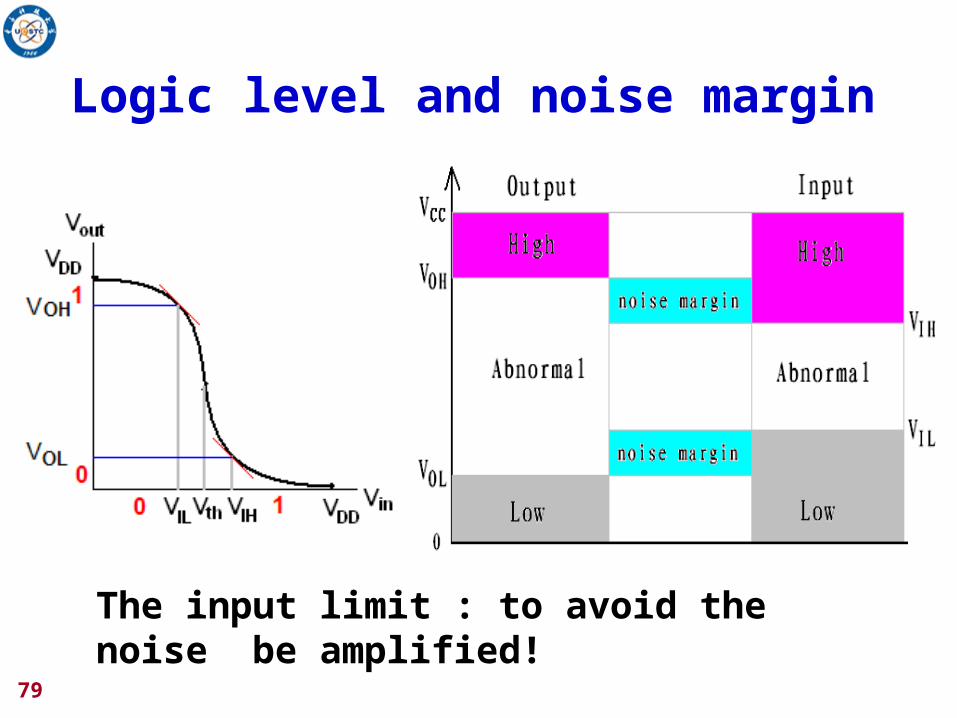
Logic level and noise margin
The input limit : to avoid the noise be amplified!
80
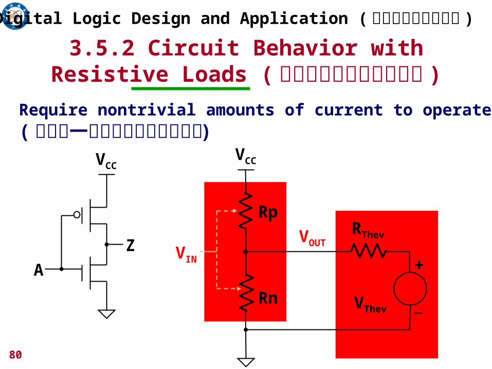
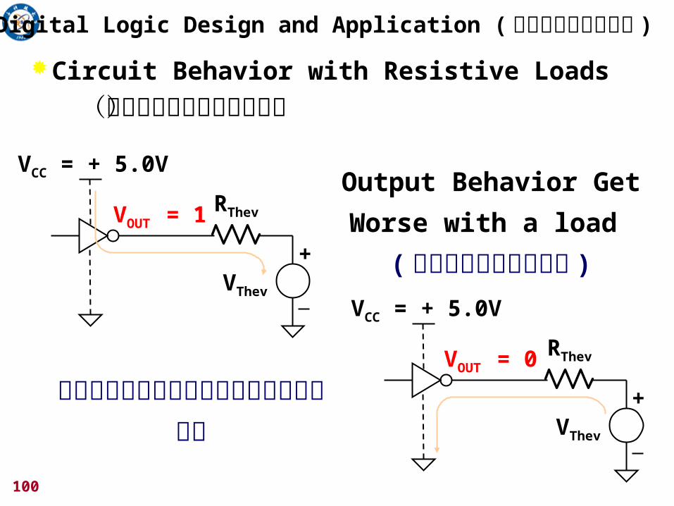
Digital Logic Design and Application ( 数字逻辑设计及应用 )3.5.2 Circuit Behavior with Resistive Loads (带电阻性负载的电
路特性 )
Require nontrivial amounts of current to operate( 要求有一定的驱动电流才能工作 )
VCC
A
Z
VCC
RThev
Rp
Rn VThev
+
VOUTVIN
81
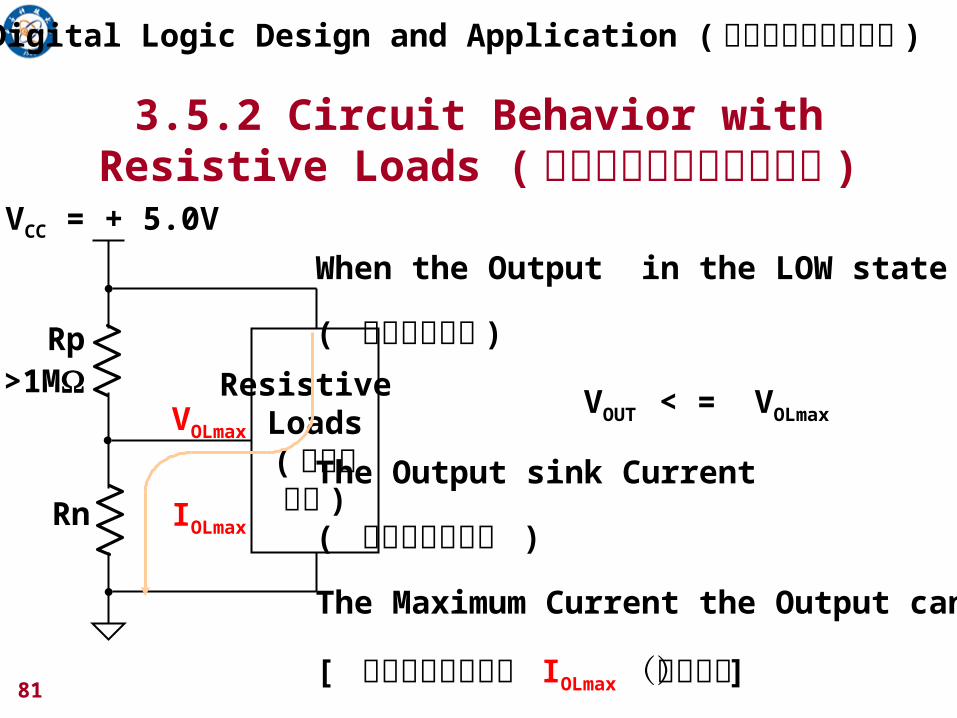
Digital Logic Design and Application ( 数字逻辑设计及应用 )
VCC = + 5.0V
Rp>1M
Rn
Resistive Loads
( 电阻性负载 )
VOLmax
IOLmax
When the Output in the LOW state
( 输出为低态时 )
VOUT < = VOLmax
The Output sink Current
( 输出端吸收电流 )
The Maximum Current the Output can sink
[ 能吸收的最大电流 IOLmax (灌电流) ]
3.5.2 Circuit Behavior with Resistive Loads (带电阻性负载的电
路特性 )
82
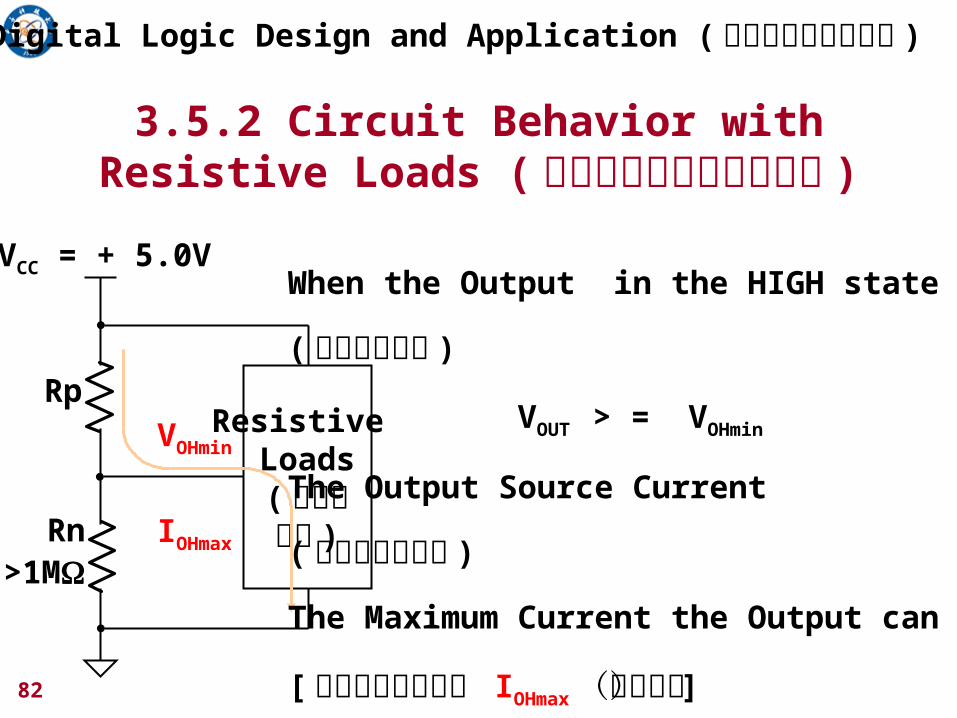
Digital Logic Design and Application ( 数字逻辑设计及应用 )
VCC = + 5.0V
Rp
Rn>1M
Resistive Loads
( 电阻性负载 )
VOHmin
IOHmax
When the Output in the HIGH state
( 输出为高态时 )
VOUT > = VOHmin
The Output Source Current
( 输出端提供电流 )
The Maximum Current the Output can Source
[ 能提供的最大电流 IOHmax (拉电流) ]
3.5.2 Circuit Behavior with Resistive Loads (带电阻性负载的电
路特性 )
83
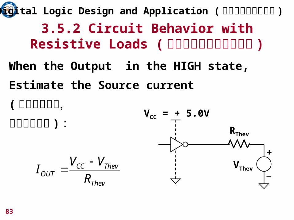
Digital Logic Design and Application ( 数字逻辑设计及应用 )
VCC = + 5.0V
RThev
VThev +
When the Output in the HIGH state,
Estimate the Source current
( 输出为高态时,估计提供电流 ) :
Thev
ThevCCOUT R
VVI
3.5.2 Circuit Behavior with Resistive Loads (带电阻性负载的电
路特性 )
84
VCC = + 5.0V
RThev
VThev +
When the Output in the LOW state,Estimate the Sink current( 输出为低态时,估计吸收电流 ) :
Thev
ThevOUT R
VI
Digital Logic Design and Application ( 数字逻辑设计及应用 )3.5.2 Circuit Behavior with Resistive Loads (带电阻性负载的电
路特性 )
85
VCC = + 5.0V
400
2.5k
VIN
1.5V
VOUT
4.31V
VCC = + 5.0V
4k
200
VIN
3.5V
VOUT
0.24V
Output voltage away from the power-supply rail (Further
with a resistive load [ 输出电压变坏(有电阻性负载时更差) ]
What’s worse: Output current , Power Consumption ( 更糟糕的是:输出端电流 ,功耗 )
3.5.3 Circuit Behavior with Non-ideal Inputs (非理想输入时的电路特性 )
86
Digital Logic Design and Application ( 数字逻辑设计及应用 )
3.5.4 Fan-out(扇出) The Number of Inputs that the Gate can drive
without exceeding its worst-case loading specifications.
(在不超出其最坏情况负载规格的条件下, 一个逻辑门能驱动的输入端个数。 ) Fan-out must be examined for both possible
output states, HIGN and LOW (扇出需考虑输出高电平和低电平两种状态 ) Overall Fan-out = Min (HIGH-state and LOW-state
[ 总扇出=min(高态扇出,低态扇出) ] DC Fan-out and AC Fan-out ( 直流扇出 和 交流扇出 )
87
Digital Logic Design and Application ( 数字逻辑设计及应用 )
74HCT Drives 74LSLOW Fan-Out ( 低态扇出 ):
Fan-out ( 扇出 )
104.0
4
mA
mA
I
I
IL
OL
HIGH Fan-Out
( 高态扇出 ) :200
20
4
A
mA
I
I
IH
OH
高态剩余驱动能力:
CMOS: 74HCT
IOH = – 4 mA
IOL = 4 mA
IIH = 1 A
IIL = – 1 A
TTL: 74LS
IOH = – 400 A
IOL = 8 mA
IIH = 20 A
IIL = – 0.4 mA
mAAmA 8.32004 总扇出
88
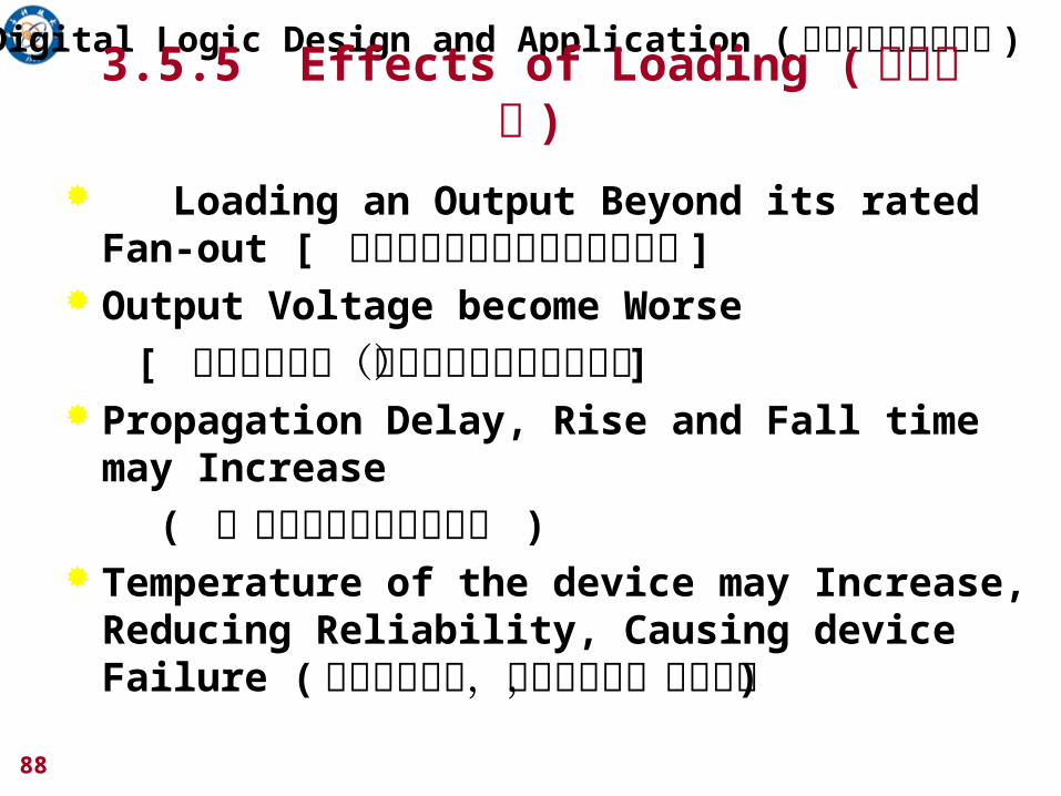
Digital Logic Design and Application ( 数字逻辑设计及应用 )3.5.5 Effects of Loading (负载效
应 )
Loading an Output Beyond its rated Fan-out [ 当输出负载大于它的扇出能力时 ]
Output Voltage become Worse
[ 输出电压变差(不符合逻辑电平的规格) ] Propagation Delay, Rise and Fall time may
Increase
( 传输延迟和转换时间变长 ) Temperature of the device may Increase,
Reducing Reliability, Causing device Failure (温度可能升高,可靠性降低,器件失效 )
89
Digital Logic Design and Application ( 数字逻辑设计及应用 )
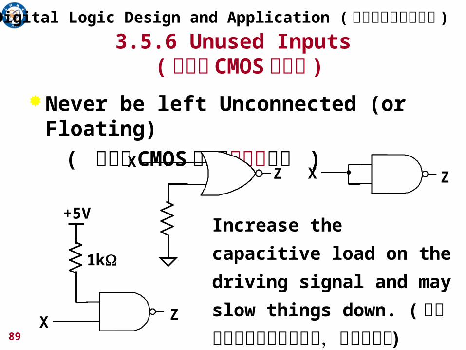
3.5.6 Unused Inputs (不用的 CMOS输入端 )
Never be left Unconnected (or Floating)
( 不用的 CMOS输入端绝不能 悬空 )
X Z
1k
+5V
X ZX
Z
Increase the capacitive
load on the driving signal
and may slow things down.
( 增加了驱动信号的电容负载,使操作变慢 )
90
Digital Logic Design and Application ( 数字逻辑设计及应用 )
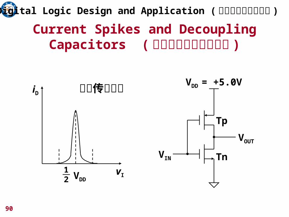
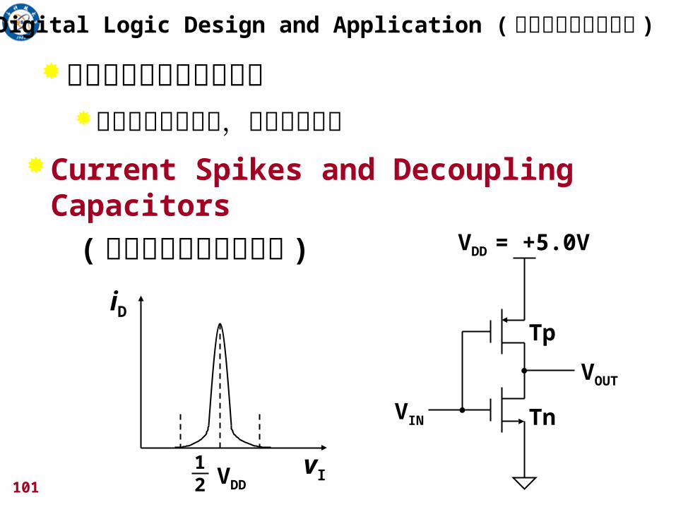
Current Spikes and Decoupling Capacitors (电流尖峰和去耦电容器 )
电流传输特性iD
vI12 VDD
VDD = +5.0V
VOUT
VIN
Tp
Tn
91
Digital Logic Design and Application ( 数字逻辑设计及应用 )
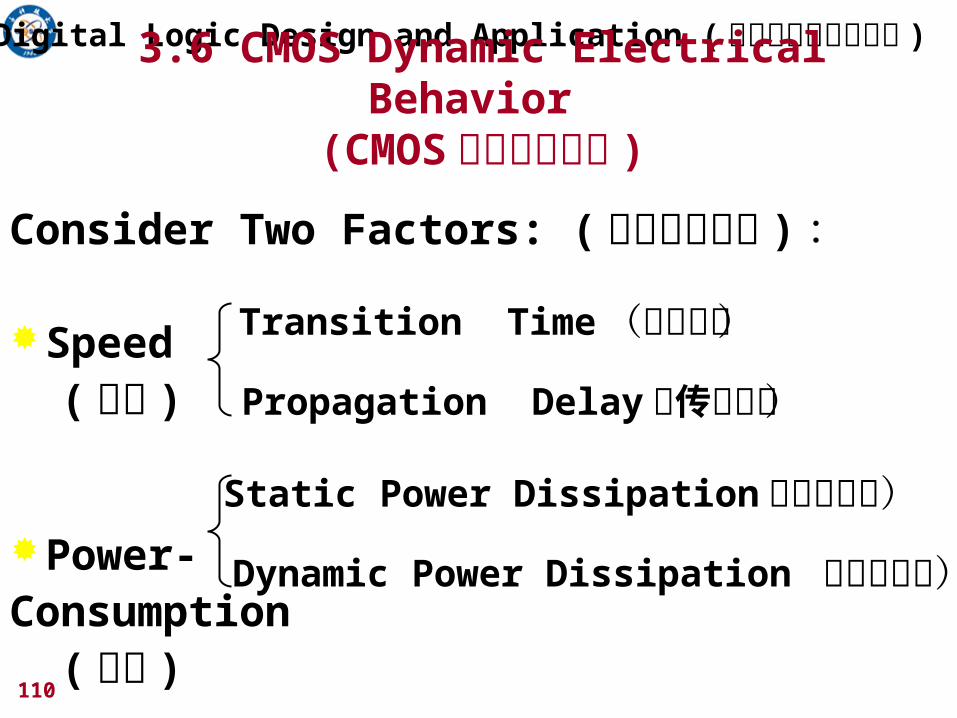
3.6 CMOS Dynamic Electrical Behavior (CMOS动态电气特性 )
Both the Speed and Power Consumption of a CMOS device depend to a large extent on AC or Dynamic Characteristics of the device and its load
( CMOS器件的速度和功耗在很大程度上取决于器件及其负载的动态特性。 )
92
3.6 CMOS Dynamic Electrical Behavior (CMOS动态电气特性 )
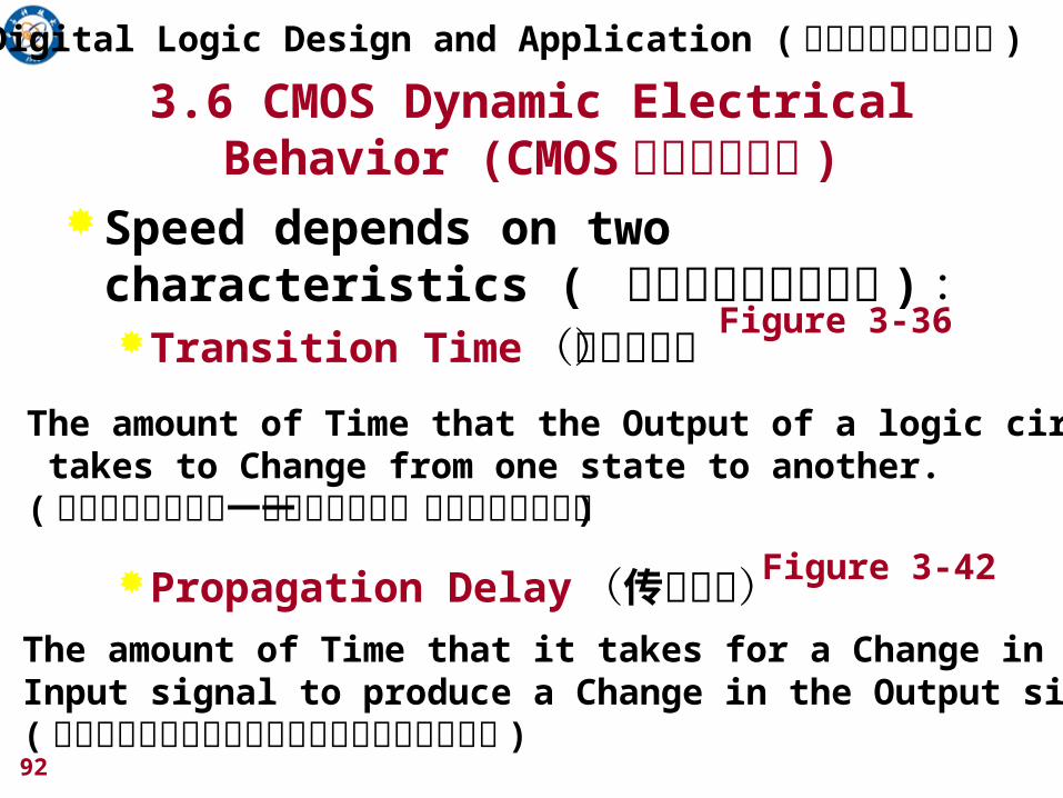
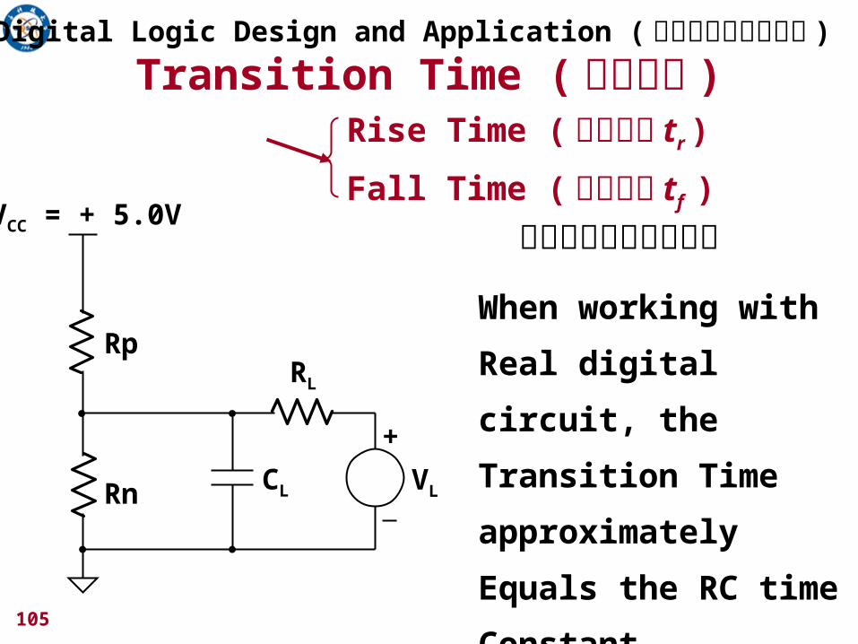
Speed depends on two characteristics ( 速度取决于两个特性 ):Transition Time(转换时间)
Propagation Delay(传播延迟)
The amount of Time that the Output of a logic circuit takes to Change from one state to another.( 逻辑电路的输出从一种状态变为另一种状态所需的时间 )
The amount of Time that it takes for a Change in the Input signal to produce a Change in the Output signal.( 从输入信号变化到产生输出信号变化所需的时间 )
Figure 3-36
Figure 3-42
Digital Logic Design and Application ( 数字逻辑设计及应用 )
93
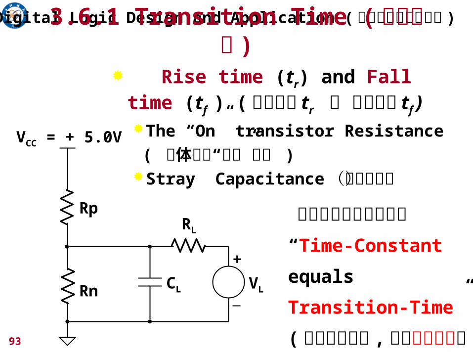
Digital Logic Design and Application ( 数字逻辑设计及应用 )3.6.1 Transition Time (转换时间 )
Rise time (tr) and Fall time (tf ) (上升时间 tr 和 下降时间 tf )The “On” transistor Resistance
( “ ” 晶体管的 导通 电阻 )Stray Capacitance(寄生电容)
VCC = + 5.0V
RL
Rp
Rn VL
+
CL
电容两端电压不能突变“Time-Constant equals
Transition-Time”
( 在实际电路中 , 可用时间常数近似转换时间 )
94
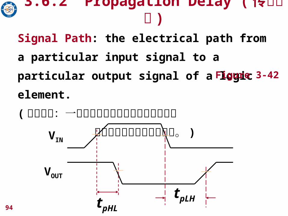
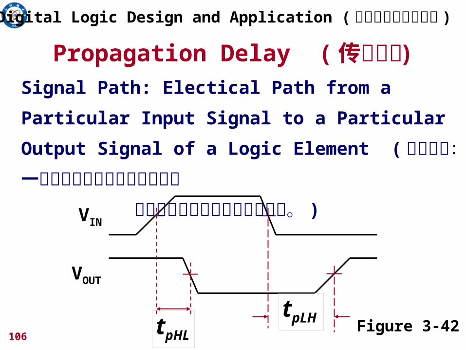
3.6.2 Propagation Delay (传播延迟 )
VIN
VOUT
Signal Path: the electrical path from a particular
input signal to a particular output signal of a
logic element.
( 信号通路:一个特定输入信号到逻辑元件的特定 输出信号所经历的电气通路。 )
Figure 3-42
pLHtpHLt
95
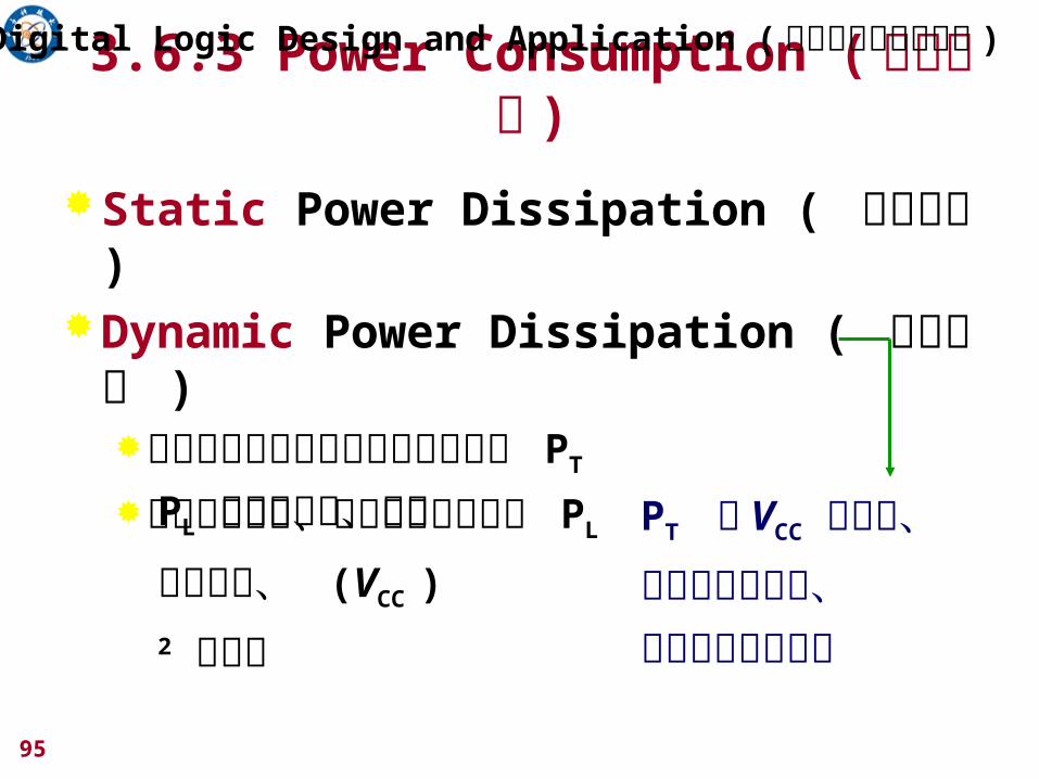
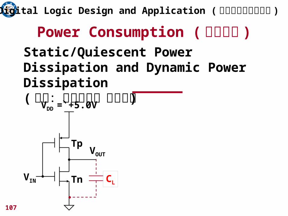
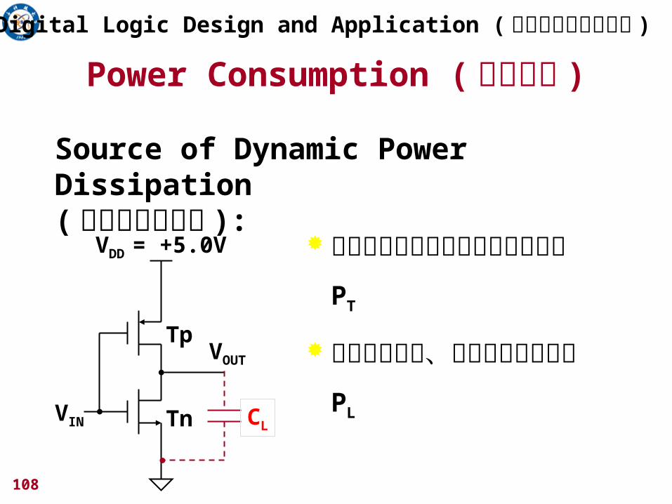
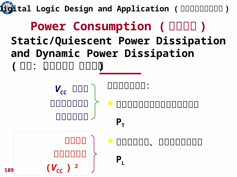
3.6.3 Power Consumption (功率损耗 )
Static Power Dissipation ( 静态功耗 )Dynamic Power Dissipation ( 动态功
耗 ) 两个管子瞬间同时导通产生的功耗 PT
对负载电容充、放电所产生的功耗 PL
PL 与负载电容、输入信号频率、 (VCC ) 2 成正比
PT 与 VCC 的大小、输入波形的好坏、输入信号频率有关
Digital Logic Design and Application ( 数字逻辑设计及应用 )
96
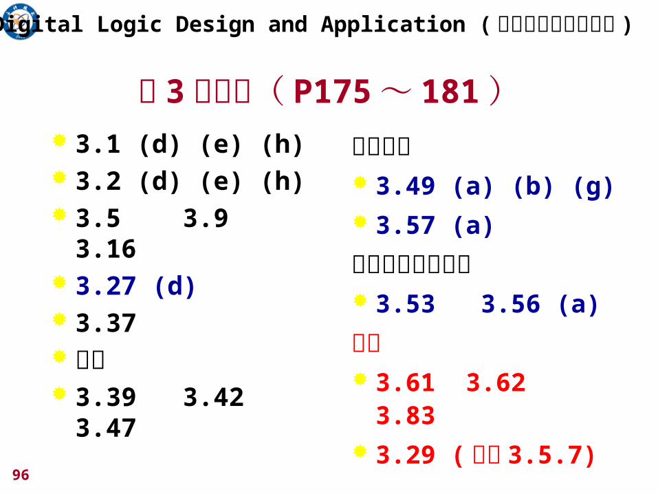
第 3章作业( P175~ 181) 3.1 (d) (e) (h) 3.2 (d) (e) (h) 3.5 3.9 3.16 3.27 (d) 3.37 理解 3.39 3.42 3.47
计算扇出 3.49 (a) (b) (g) 3.57 (a)
计算直流噪声容限 3.53 3.56 (a)
选做 3.61 3.62 3.83 3.29 (自学 3.5.7)
Digital Logic Design and Application ( 数字逻辑设计及应用 )
97
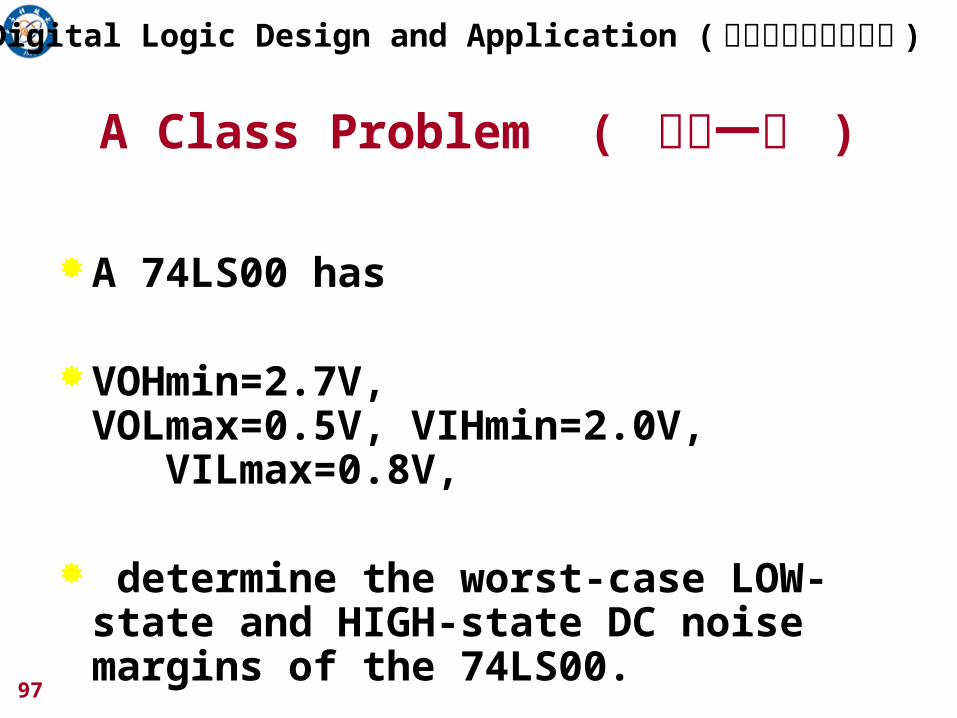
A Class Problem ( 每课一题 )
A 74LS00 has
VOHmin=2.7V, VOLmax=0.5V, VIHmin=2.0V, VILmax=0.8V,
determine the worst-case LOW-state and HIGH-state DC noise margins of the 74LS00.
Digital Logic Design and Application ( 数字逻辑设计及应用 )

98
Chapter 3 Digital Circuits (数字电路 )
Give a knowledge of the Electrical aspects of Digital Circuits
(介绍数字电路中的电气知识 )
Digital Logic Design and Application ( 数字逻辑设计及应用 )
99
CMOS Steady-State Electrical Behavior
( CMOS稳态电气特性)
Logic Levels
(逻辑电压电平)
Noise Margin
(噪声容限)
高态
不正常状态
低态VOLmax
VILmax
VIHmin
VOHmin
Digital Logic Design and Application ( 数字逻辑设计及应用 )
Review of Chapter 3
100
VOUT = 0
VCC = + 5.0V
RThev
VThev +
VCC = + 5.0V
RThev
VThev +
VOUT = 1
Circuit Behavior with Resistive Loads
(带电阻性负载的电路特性)
保证提供或吸收的电流小于门电路的规定值
Output Behavior Get
Worse with a load
( 负载导致输出特性变坏 )
Digital Logic Design and Application ( 数字逻辑设计及应用 )
101
非理想输入时的电路特性输入偏离供电轨道,输出电压变坏
VDD = +5.0V
VOUT
VIN
Tp
Tn
Current Spikes and Decoupling Capacitors
( 电流尖峰和去耦电容器 )
iD
vI12 VDD
Digital Logic Design and Application ( 数字逻辑设计及应用 )
102
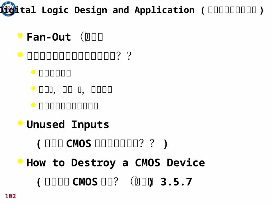
Fan-Out(扇出)
当输出负载大于它的扇出能力时?? 输出特性变差 电流,功耗 ,温度升高 传输延迟、转换时间变长
Unused Inputs
(不用的 CMOS输入端如何处理?? )
How to Destroy a CMOS Device
(如何毁坏 CMOS器件?(自学) ) 3.5.7
Digital Logic Design and Application ( 数字逻辑设计及应用 )
103
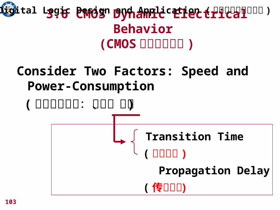
3.6 CMOS Dynamic Electrical Behavior
(CMOS动态电气特性 )
Consider Two Factors: Speed and Power-Consumption
(考虑两个方面:速度、功耗 )
Transition Time
( 转换时间 )
Propagation Delay
( 传播延迟 )
Digital Logic Design and Application ( 数字逻辑设计及应用 )
104
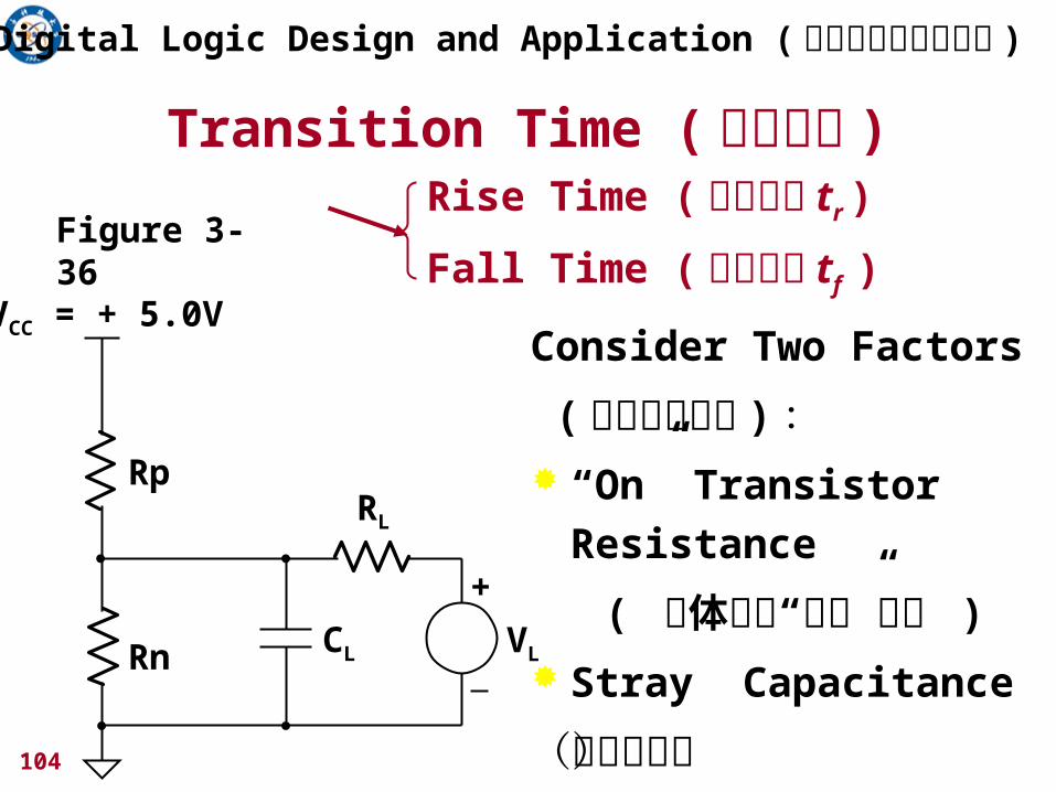
Transition Time (转换时间 )
Consider Two Factors
(考虑两个因素 ): “On” Transistor
Resistance
( “ ” 晶体管的 导通 电阻 )
Stray Capacitance
(寄生电容)
VCC = + 5.0V
RL
Rp
Rn VL
+
CL
Figure 3-36Rise Time ( 上升时间 tr )
Fall Time ( 下降时间 tf )
Digital Logic Design and Application ( 数字逻辑设计及应用 )
105
VCC = + 5.0V
RL
Rp
Rn VL
+
CL
电容两端电压不能突变
When working with
Real digital circuit, the
Transition Time
approximately Equals
the RC time Constant( 在实际电路中可用时间常数近似转换时间 )
Digital Logic Design and Application ( 数字逻辑设计及应用 )
Transition Time (转换时间 )Rise Time ( 上升时间 tr )
Fall Time ( 下降时间 tf )
106
Propagation Delay (传播延迟 )
Figure 3-42
VIN
VOUT
pLHtpHLt
Signal Path: Electical Path from a Particular Input
Signal to a Particular Output Signal of a Logic
Element ( 信号通路:一个特定输入信号到逻辑元件的 特定输出信号所经历的电气通路。 )
Digital Logic Design and Application ( 数字逻辑设计及应用 )
107
Power Consumption (功率损耗 )
VDD = +5.0V
VOUT
VIN
Tp
Tn
Static/Quiescent Power Dissipation and Dynamic Power Dissipation( 分为:静态功耗、动态功耗 )
CL
Digital Logic Design and Application ( 数字逻辑设计及应用 )
108
Power Consumption (功率损耗 )
两个管子瞬间同时导通
产生的功耗 PT
对负载电容充、放电所
产生的功耗 PL
VDD = +5.0V
VOUT
VIN
Tp
Tn
Source of Dynamic Power Dissipation( 动态功耗的来源 ):
CL
Digital Logic Design and Application ( 数字逻辑设计及应用 )
109
动态功耗的来源:
两个管子瞬间同时导通
产生的功耗 PT
对负载电容充、放电所
产生的功耗 PL
VCC 的大小输入波形的好坏
输入信号频率
负载电容输入信号频率
(VCC ) 2
Digital Logic Design and Application ( 数字逻辑设计及应用 )Power Consumption (功率损耗 )
Static/Quiescent Power Dissipation and Dynamic Power Dissipation( 分为:静态功耗、动态功耗 )
110
Consider Two Factors: (考虑两个方面 ):
Speed (速度 )
Power-Consumption (功耗 )
Transition Time (转换时间)
Propagation Delay (传播延迟)
Static Power Dissipation (静态功耗)
Dynamic Power Dissipation (动态功耗)
Digital Logic Design and Application ( 数字逻辑设计及应用 )3.6 CMOS Dynamic Electrical Behavior
(CMOS动态电气特性 )
111
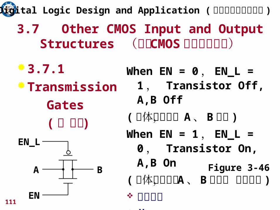
3.7 Other CMOS Input and Output Structures (其他 CMOS输入输出结构)
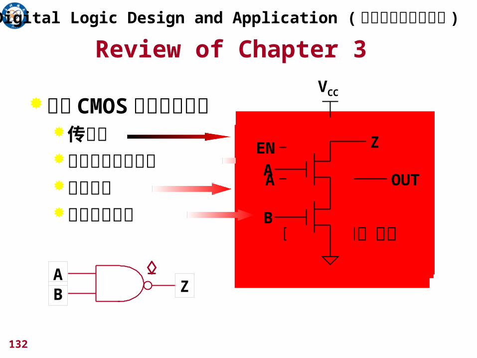
3.7.1 Transmission
Gates
(传输门 )
When EN = 0, EN_L = 1 , Transistor Off, A,B Off
( 晶体管截止, A、 B 断开 )
When EN = 1, EN_L = 0 , Transistor On, A,B On
( 晶体管导通, A、 B 之间低 阻抗连接 )
双向器件 传播延迟非常短
EN
EN_L
A B
Digital Logic Design and Application ( 数字逻辑设计及应用 )
Figure 3-46
112
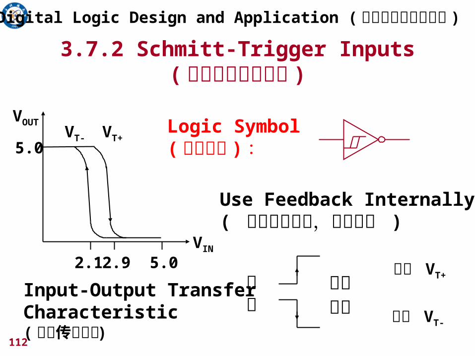
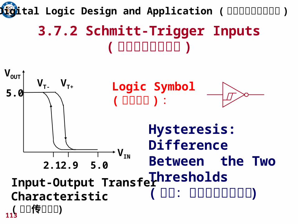
3.7.2 Schmitt-Trigger Inputs(施密特触发器输入 )
VOUT
VIN
5.02.1 2.9
5.0
Input-Output TransferCharacteristic( 电压传输特性 )
VT+VT-
输入
门限电压
正向 VT+
负向 VT-
Use Feedback Internally( 采用内部反馈,边沿更陡 )
Logic Symbol( 逻辑符号 ) :
Digital Logic Design and Application ( 数字逻辑设计及应用 )
113
3.7.2 Schmitt-Trigger Inputs(施密特触发器输入 )
VOUT
VIN
5.02.1 2.9
5.0
Input-Output TransferCharacteristic( 电压传输特性 )
VT+VT-
Hysteresis: Difference Between the Two Thresholds( 滞后:两个门限电压之差 )
Digital Logic Design and Application ( 数字逻辑设计及应用 )
Logic Symbol( 逻辑符号 ) :
114
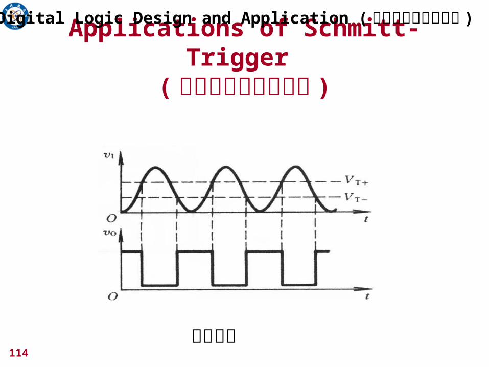
Applications of Schmitt-Trigger
(施密特触发器的应用 )
波形变换
Digital Logic Design and Application ( 数字逻辑设计及应用 )
115
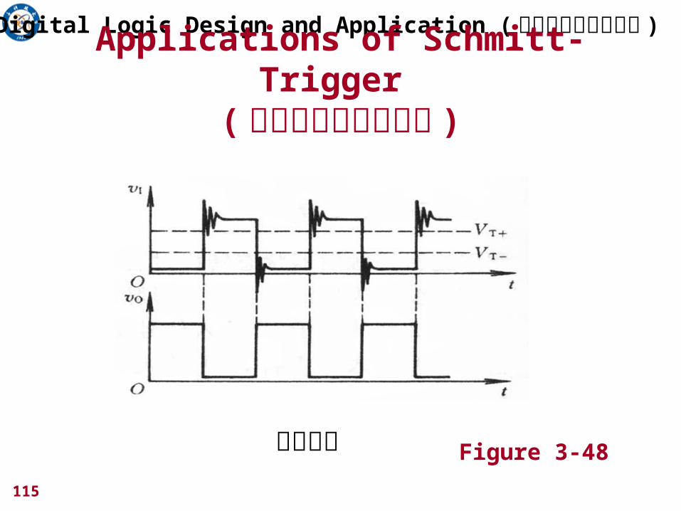
脉冲整形
Digital Logic Design and Application ( 数字逻辑设计及应用 )Applications of Schmitt-Trigger
(施密特触发器的应用 )
Figure 3-48
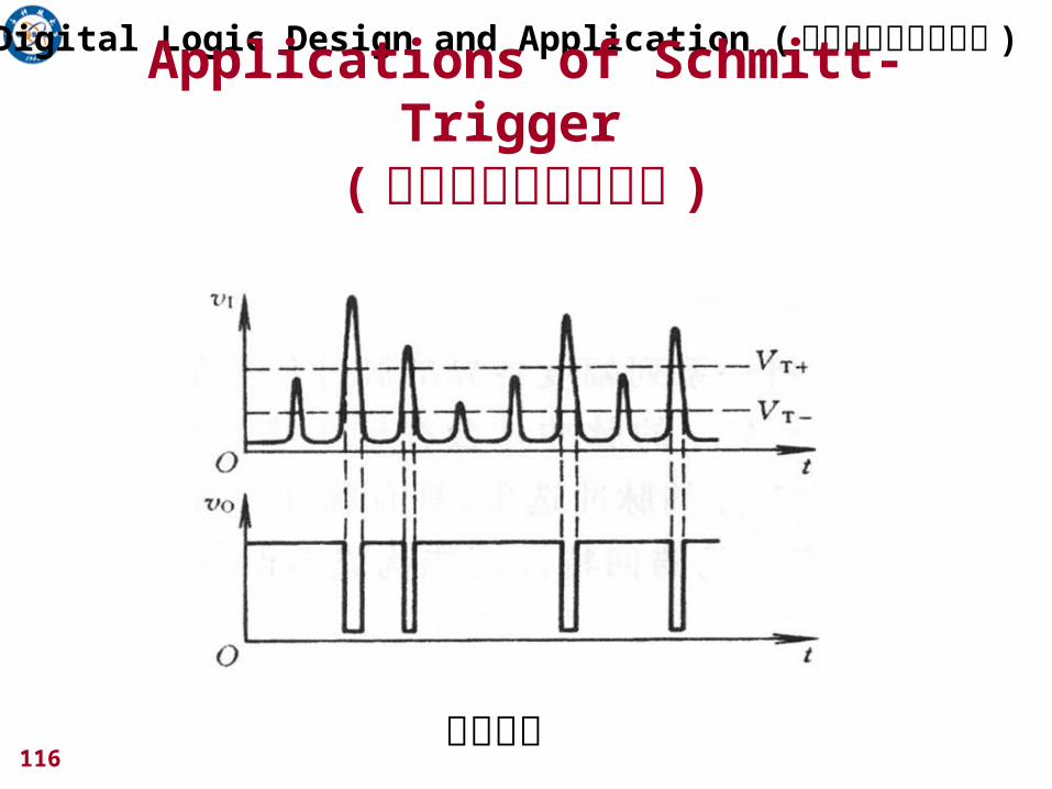
116脉冲鉴幅
Digital Logic Design and Application ( 数字逻辑设计及应用 )Applications of Schmitt-Trigger
(施密特触发器的应用 )
117
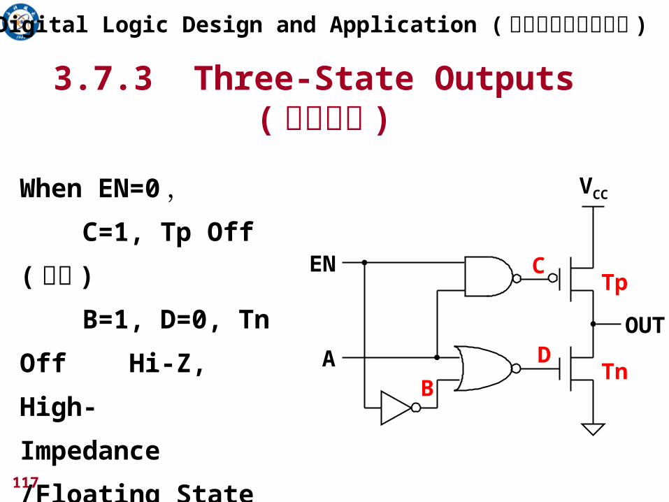
3.7.3 Three-State Outputs (三态输出 )
VCC
OUT
EN
A
When EN=0 , C=1, Tp Off ( 截止 )
B=1, D=0, Tn
Off Hi-Z, High-
Impedance
/Floating State
( 高阻态 / 悬空态)
B
C
D
Tp
Tn
Digital Logic Design and Application ( 数字逻辑设计及应用 )
118
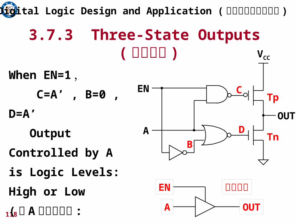
3.7.3 Three-State Outputs (三态输出 ) VCC
OUT
EN
A
When EN=1 , C=A’ , B=0 ,
D=A’
Output
Controlled by A is
Logic Levels:
High or Low
( 由 A 控制输出为 :
逻辑 0 或 逻辑 1)
B
C
D
Tp
Tn
A
EN
OUT
逻辑符号
Digital Logic Design and Application ( 数字逻辑设计及应用 )
119
输出电平??造成逻辑混乱
很大的负载电流同时流过输出级可使门电路损坏
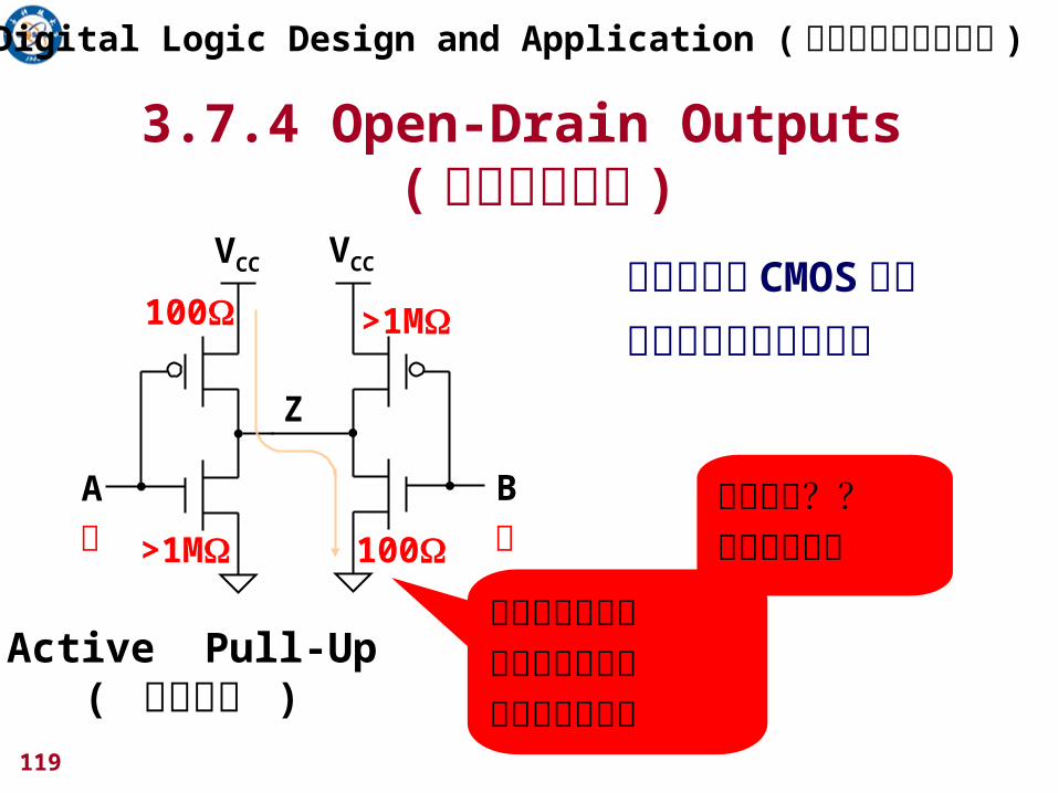
3.7.4 Open-Drain Outputs (漏极开路输出 )
VCC
A
Z
Active Pull-Up( 有源上拉 )
VCC
B
低 高
有源上拉的 CMOS 器件其输出端不能直接相联
100
>1M100
>1M
Digital Logic Design and Application ( 数字逻辑设计及应用 )
120
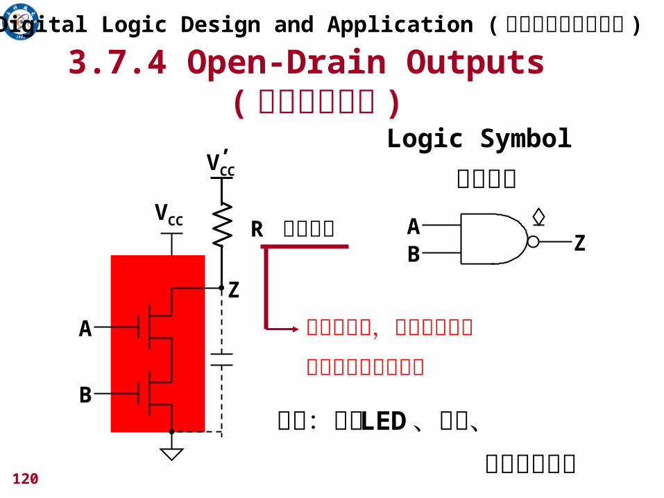
A
B
Z
VCC
VCC’
R 上拉电阻 AB Z
逻辑符号
希望尽量小,减少上升时间太小则吸收电流太大
应用:驱动 LED 、线与、 驱动多源总线
Digital Logic Design and Application ( 数字逻辑设计及应用 )
3.7.4 Open-Drain Outputs (漏极开路输出 )
Logic Symbol
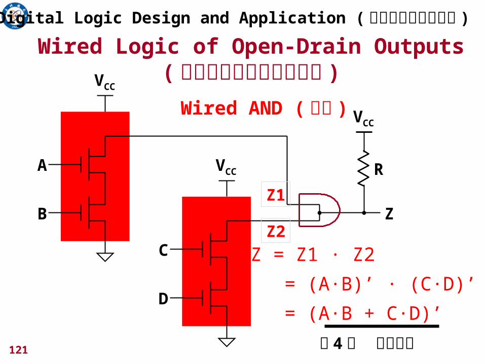
121
A
B Z
VCC
VCC
R
C
D
VCC
Z = Z1 · Z2
= (A·B)’ · (C·D)’
= (A·B + C·D)’
Wired Logic of Open-Drain Outputs(漏极开路输出的线连逻辑 )
Z1
Z2
Wired AND ( 线与 )
第 4 章 反演定理
Digital Logic Design and Application ( 数字逻辑设计及应用 )
122
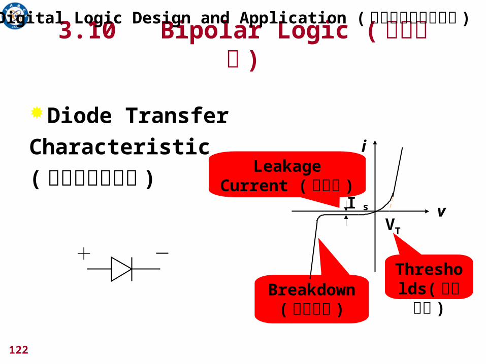
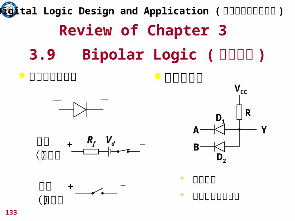
3.10 Bipolar Logic (双极逻辑 )
Diode Transfer
Characteristic
(二极管开关特性 )
Thresholds( 门限电压 )
Breakdown( 反向击穿 )
Leakage Current ( 漏电流 )
v
i
VT
I s
+
Digital Logic Design and Application ( 数字逻辑设计及应用 )
123
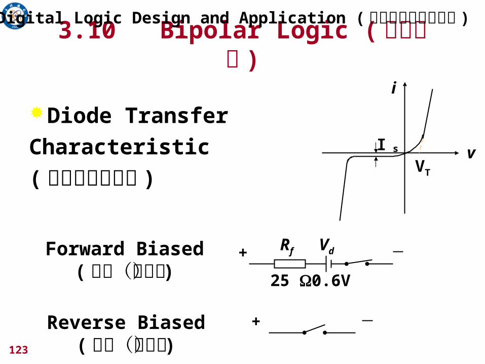
3.10 Bipolar Logic (双极逻辑 )
Diode Transfer
Characteristic
(二极管开关特性 )v
i
VT
I s
Digital Logic Design and Application ( 数字逻辑设计及应用 )
+ Rf VdForward Biased( 正偏(导通) )
+Reverse Biased( 反偏(截止) )
25 0.6V
124
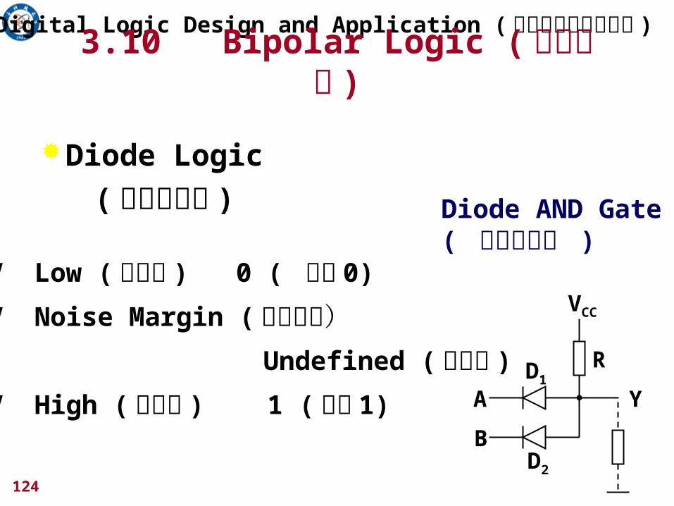
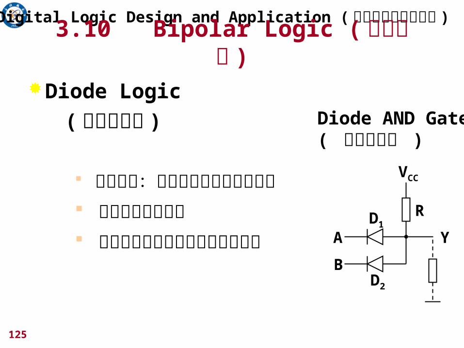
Diode Logic
(二极管逻辑 )
A
B
D1
D2
R
VCC
Y
0~ 2V Low ( 低电平 ) 0 ( 逻辑 0)
2~ 3V Noise Margin ( 噪声电平) Undefined (未定义 )
3~ 5V High ( 高电平 ) 1 ( 逻辑 1)
Diode AND Gate( 二极管与门 )
Digital Logic Design and Application ( 数字逻辑设计及应用 )
3.10 Bipolar Logic (双极逻辑 )
125
Diode Logic
(二极管逻辑 )
A
B
D1
D2
R
VCC
Y
电平偏移:输出和输入的数值不相等 不能直接驱动负载 通常用于集成电路内部的逻辑单元
Diode AND Gate( 二极管与门 )
Digital Logic Design and Application ( 数字逻辑设计及应用 )
3.10 Bipolar Logic (双极逻辑 )
126
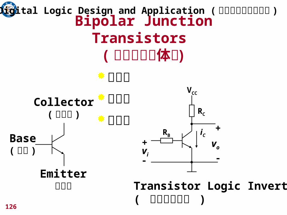
Bipolar Junction Transistors (双极结型晶体管 )
截止区放大区饱和区
Base( 基极 )
Collector(集电极 )
Emitter发射极
VCC
vo
+
-vi
+
-
RB
RC
iC
Transistor Logic Inverter( 三极管反相器 )
Digital Logic Design and Application ( 数字逻辑设计及应用 )
127
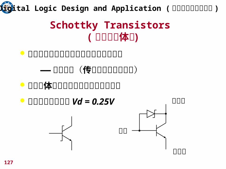
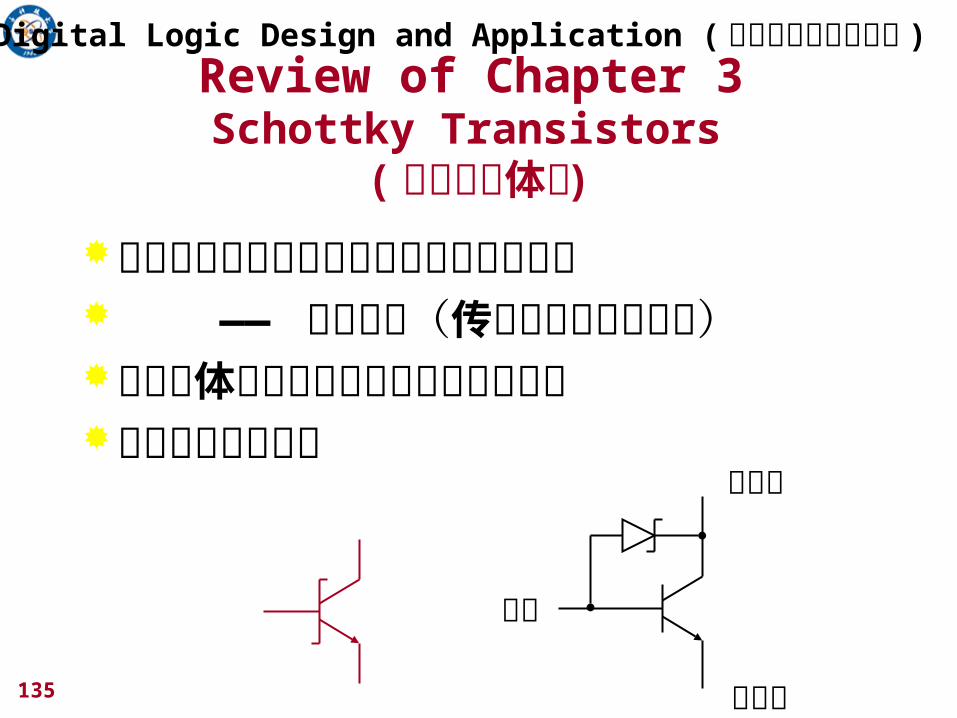
Schottky Transistors (肖特基晶体管 )
三极管内部电荷的建立和消散都需要时间
——存储时间(传输延迟的重要部分)
确保晶体管正常工作时不进入深度饱和
利用肖特基二极管 Vd = 0.25V
基极
集电极
发射极
Digital Logic Design and Application ( 数字逻辑设计及应用 )
128
Chapter 3 Digital Circuits (数字电路 )
Give a knowledge of the Electrical aspects of Digital Circuits
(介绍数字电路中的电气知识 )
Digital Logic Design and Application ( 数字逻辑设计及应用 )
129
Digital Logic Design and Application ( 数字逻辑设计及应用 )
Review of Chapter 3CMOS Steady-State Electrical Behavior
(CMOS稳态电气特性 )
Logic Voltage Levels and Noise Margins
(逻辑电压电平和噪声容限 )
Circuit Behavior with Resistive Loads
(带电阻性负载的电路特性 )
Non-ideal Inputs, Current Spikes, and Decoupling
Capacitors (非理想输入、电流尖峰和去耦电容器 )
Unused Inputs (不用的 CMOS输入端 )
130
Review of Chapter 3
Digital Logic Design and Application ( 数字逻辑设计及应用 )
CMOS Dynamic Electrical Behavior (CMOS 动态电气特性 )
• Speed: Transition Time and Propagation Delay ( 速度:转换时间、传播延迟 )• Power Consumption: Static and Dynamic Power Dissipation ( 功耗:静态、动态 )

131
CMOS Steady-State Electrical Behavior
( CMOS稳态电气特性)
Logic Levels
(逻辑电压电平)
Noise Margin
(噪声容限)
高态
不正常状态
低态VOLmax
VILmax
VIHmin
VOHmin
Digital Logic Design and Application ( 数字逻辑设计及应用 )
Review of Chapter 3
132
Review of Chapter 3Digital Logic Design and Application ( 数字逻辑设计及应用 )
其他 CMOS 输入输出结构传输门施密特触发器输入三态输出漏极开路输出
EN
EN_L
A B
AB Z
逻辑符号:A
EN
OUT
高阻态、低态、高态
A
B
Z
VCC
133
Digital Logic Design and Application ( 数字逻辑设计及应用 )
Review of Chapter 3
二极管开关特性 二极管逻辑
+
+ Rf Vd正偏(导通)
+反偏(截止)
A
B
D1
D2
R
VCC
Y
电平偏移 不能直接驱动负载
3.9 Bipolar Logic (双极逻辑 )
134
Review of Chapter 3
截止区放大区饱和区
基极base
collector集电极
发射极emitter
VCC
vo
+
-vi
+
-
RB
RC
iC
三极管反相器
Digital Logic Design and Application ( 数字逻辑设计及应用 )
Bipolar Junction Transistors (双极结型晶体管 )
135
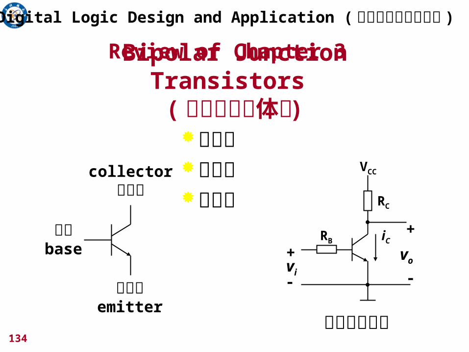
Review of Chapter 3
三极管内部电荷的建立和消散都需要时间 —— 存储时间(传输延迟的重要部分)
确保晶体管正常工作时不进入深度饱和利用肖特基二极管
Digital Logic Design and Application ( 数字逻辑设计及应用 )
Schottky Transistors (肖特基晶体管 )
基极
集电极
发射极
136
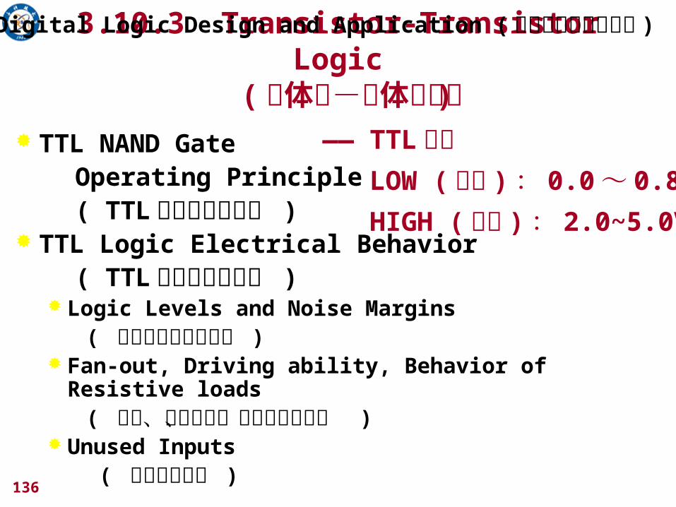
3.10.3 Transistor-Transistor Logic
(晶体管-晶体管逻辑 ) TTL NAND Gate Operating Principle ( TTL 与非门工作原理 ) TTL Logic Electrical Behavior ( TTL 逻辑的电气特性 )
Logic Levels and Noise Margins ( 逻辑电平和噪声容限 ) Fan-out, Driving ability, Behavior of Resistive loads ( 扇出、驱动能力、电阻性负载特性 ) Unused Inputs ( 不用的输入端 )
—— TTL系列 LOW ( 低态 ) : 0.0~ 0.8V
HIGH ( 高态 ) : 2.0~5.0V
Digital Logic Design and Application ( 数字逻辑设计及应用 )
137
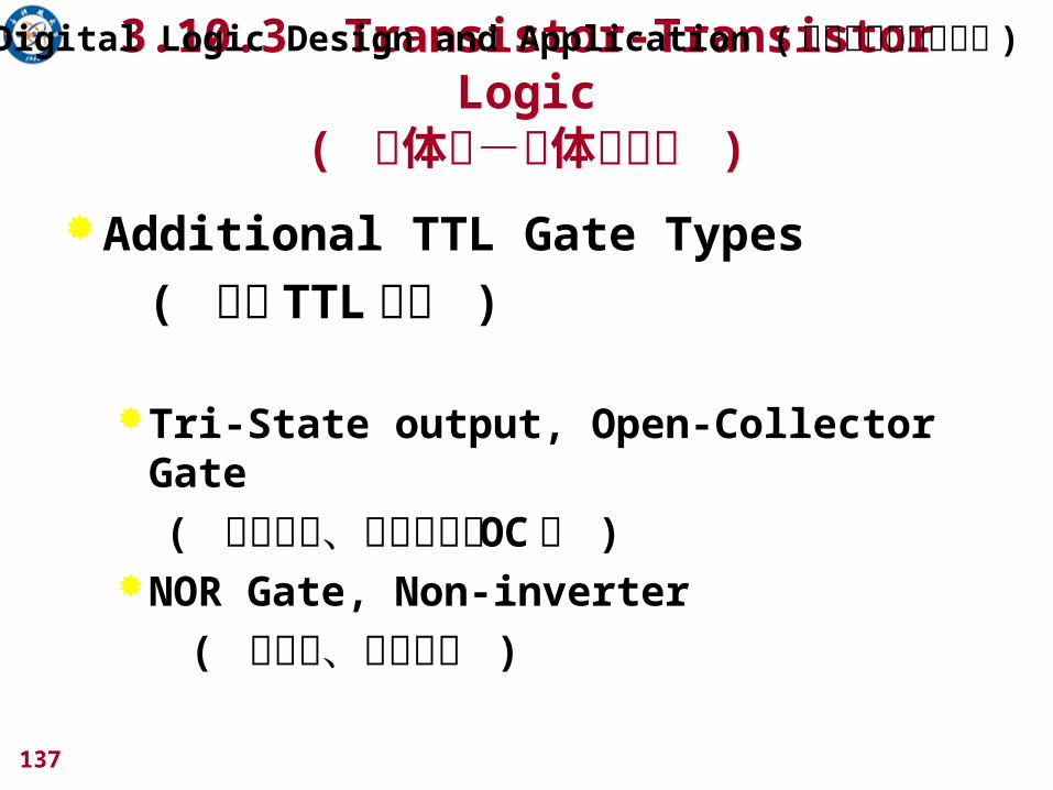
Additional TTL Gate Types
( 其它 TTL 电路 )
Tri-State output, Open-Collector Gate
( 三态输出、集电极开路 OC 门 )NOR Gate, Non-inverter
( 或非门、非反相门 )
3.10.3 Transistor-Transistor Logic
( 晶体管-晶体管逻辑 )
Digital Logic Design and Application ( 数字逻辑设计及应用 )
138
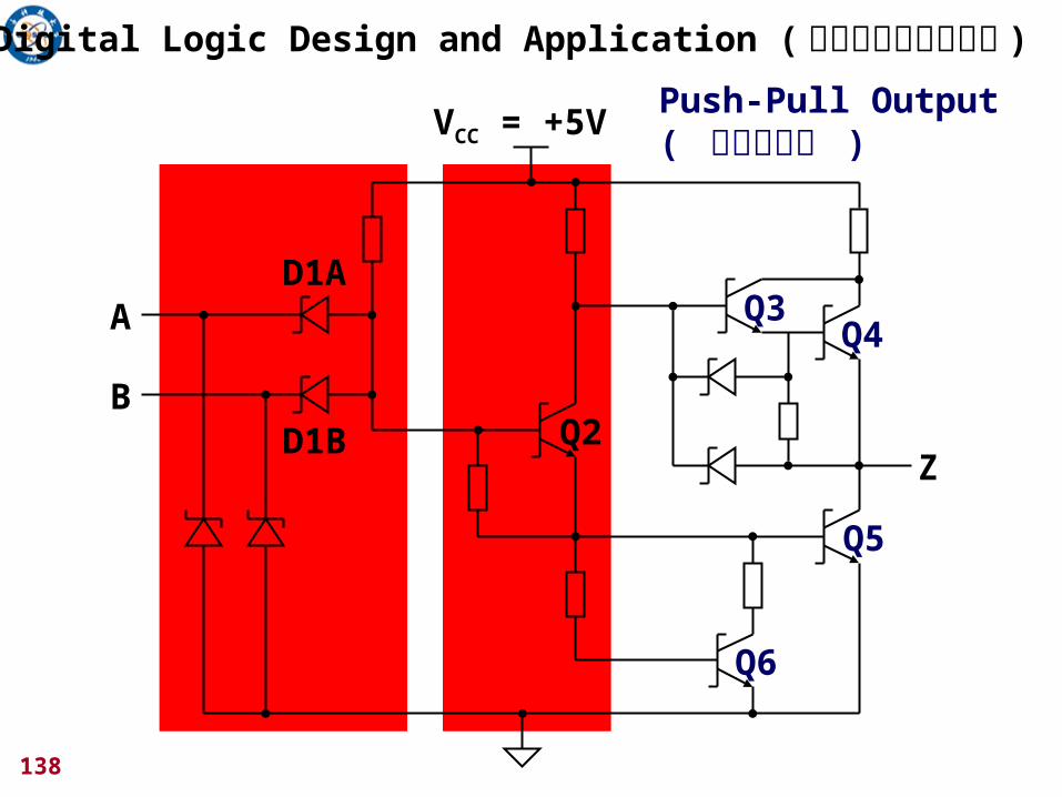
A
B
Z
VCC = +5V
Q2
Q3Q4
Q5
Q6
D1A
D1B
Push-Pull Output( 推拉式输出 )
Digital Logic Design and Application ( 数字逻辑设计及应用 )
139
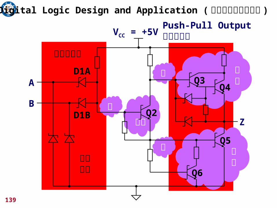
Push-Pull Output推拉式输出
二极管与门
输入保护
低
导通
截止
截止
高
低
A
B
Z
VCC = +5V
Q2
Q3Q4
Q5
Q6
D1A
D1B
Digital Logic Design and Application ( 数字逻辑设计及应用 )
140
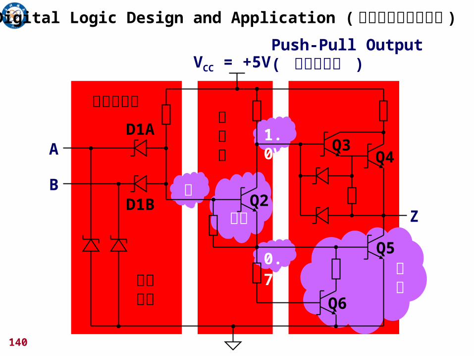
Digital Logic Design and Application ( 数字逻辑设计及应用 )
分相器
二极管与门
输入保护
高
导通
导通
1.0V
0.7V
A
B
Z
VCC = +5V
Q2
Q3Q4
Q5
Q6
D1A
D1B
Push-Pull Output( 推拉式输出 )
141
Digital Logic Design and Application ( 数字逻辑设计及应用 )
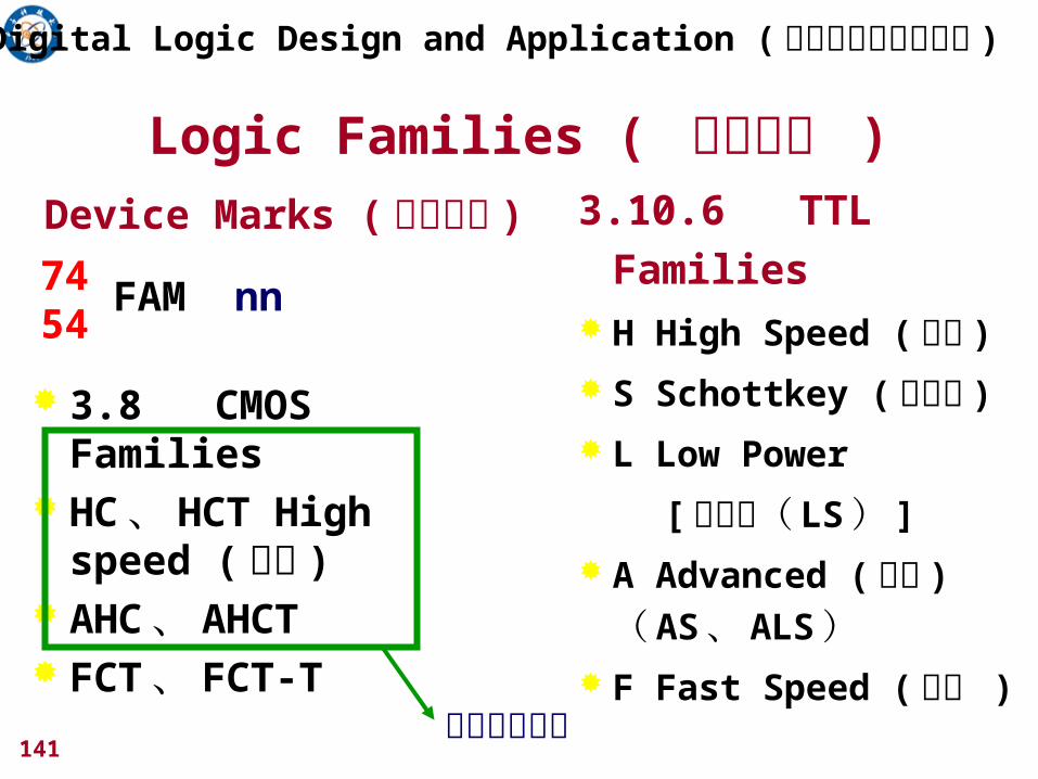
Logic Families ( 逻辑系列 )
3.8 CMOS Families HC、 HCT High
speed (高速 ) AHC、 AHCT FCT、 FCT-T
3.10.6 TTL Families
H High Speed (高速 )
S Schottkey (肖特基 )
L Low Power
[低功耗( LS) ]
A Advanced (高级 )
( AS、 ALS) F Fast Speed ( 快速 )
7454 FAM nn
Device Marks ( 器件标号 )
对称输出驱动
142
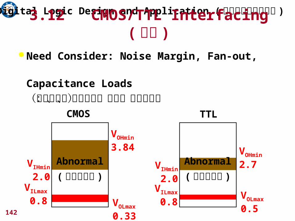
Digital Logic Design and Application ( 数字逻辑设计及应用 )3.12 CMOS/TTL Interfacing (接口 )
Need Consider: Noise Margin, Fan-out,
Capacitance Loads
(需要考虑:噪声容限、扇出、电容负载)
Abnormal
( 不正常状态 )
VOLmax
0.5
VOHmin
2.7VIHmin
2.0VILmax
0.8
TTL
Abnormal
( 不正常状态 )
VOLmax
0.33
VILmax
0.8
VIHmin
2.0
VOHmin
3.84
CMOS
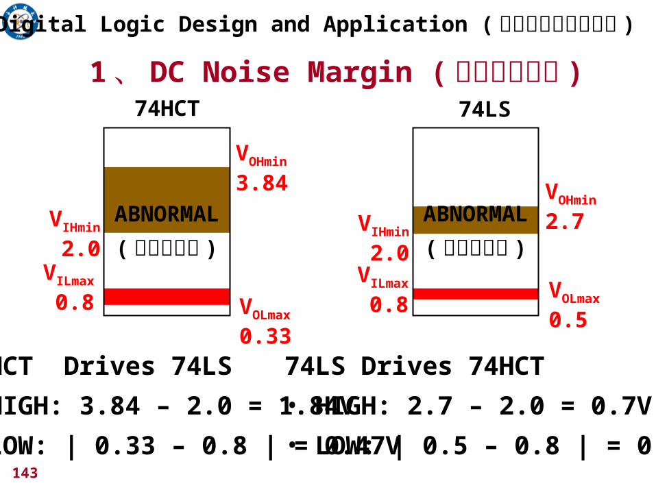
143
74HCT Drives 74LS
• HIGH: 3.84 – 2.0 = 1.84V
• LOW: | 0.33 – 0.8 | = 0.47V
ABNORMAL
( 不正常状态 )
VOLmax
0.33
VILmax
0.8
VIHmin
2.0
VOHmin
3.84
74HCT
ABNORMAL
( 不正常状态 )
VOLmax
0.5
VOHmin
2.7VIHmin
2.0VILmax
0.8
74LS
74LS Drives 74HCT
• HIGH: 2.7 – 2.0 = 0.7V
• LOW: | 0.5 – 0.8 | = 0.3V
1、DC Noise Margin ( 直流噪声容限 )
Digital Logic Design and Application ( 数字逻辑设计及应用 )
144
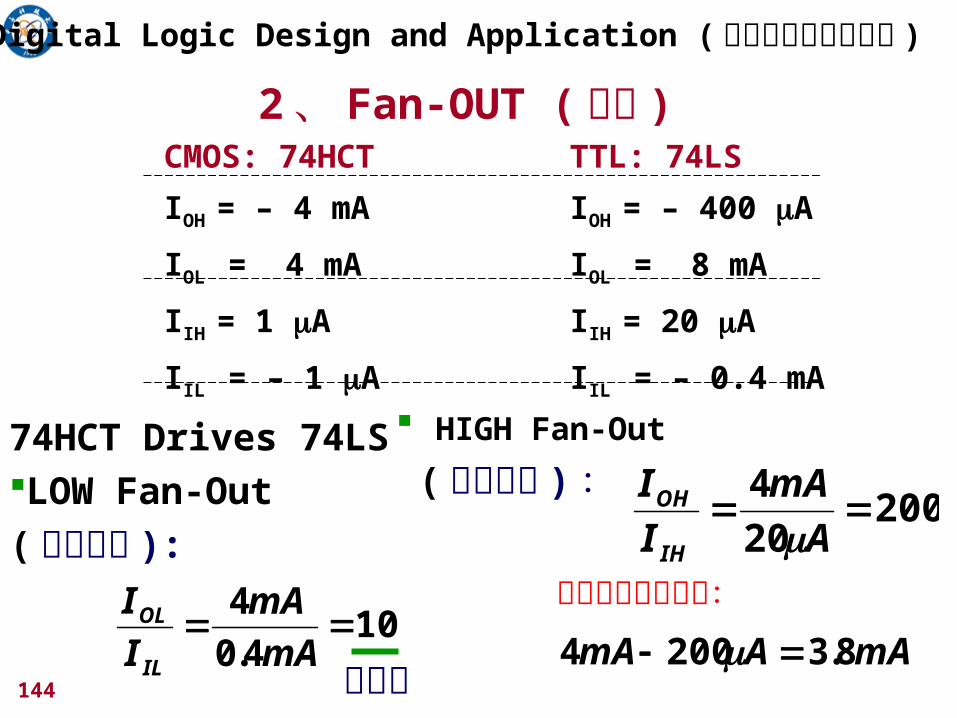
Digital Logic Design and Application ( 数字逻辑设计及应用 )
74HCT Drives 74LSLOW Fan-Out ( 低态扇出 ):
2、 Fan-OUT ( 扇出 )
104.0
4
mA
mA
I
I
IL
OL
HIGH Fan-Out
( 高态扇出 ) :200
20
4
A
mA
I
I
IH
OH
高态剩余驱动能力:
CMOS: 74HCT
IOH = – 4 mA
IOL = 4 mA
IIH = 1 A
IIL = – 1 A
TTL: 74LS
IOH = – 400 A
IOL = 8 mA
IIH = 20 A
IIL = – 0.4 mA
mAAmA 8.32004 总扇出
145
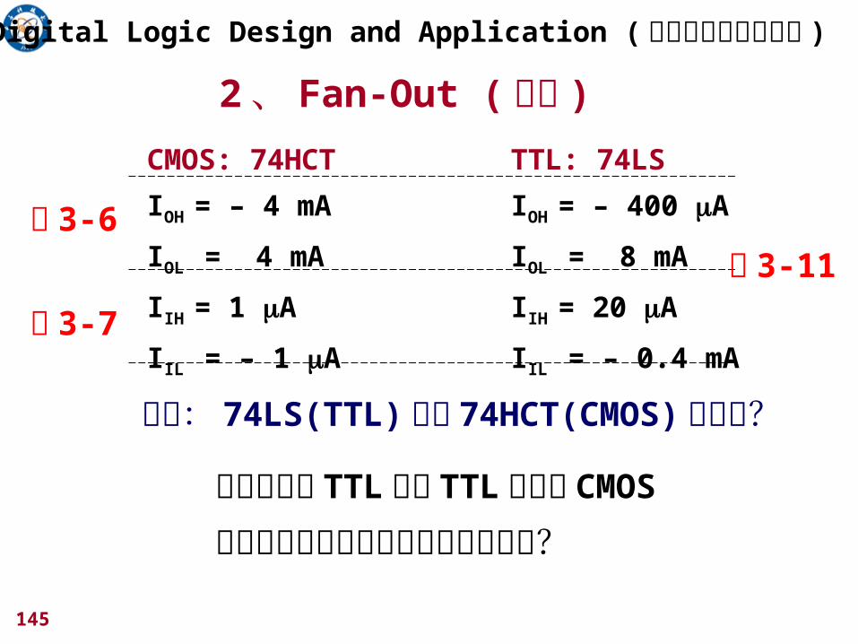
Digital Logic Design and Application ( 数字逻辑设计及应用 )
2、 Fan-Out ( 扇出 )
CMOS: 74HCT
IOH = – 4 mA
IOL = 4 mA
IIH = 1 A
IIL = – 1 A
TTL: 74LS
IOH = – 400 A
IOL = 8 mA
IIH = 20 A
IIL = – 0.4 mA
思考: 74LS(TTL) 驱动 74HCT(CMOS) 的情况?
为什么说用 TTL 驱动 TTL兼容的 CMOS
输入端几乎不用考虑直流扇出的限制?
表 3-6
表 3-7
表 3-11
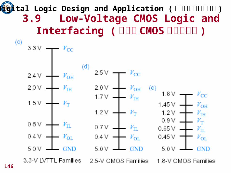
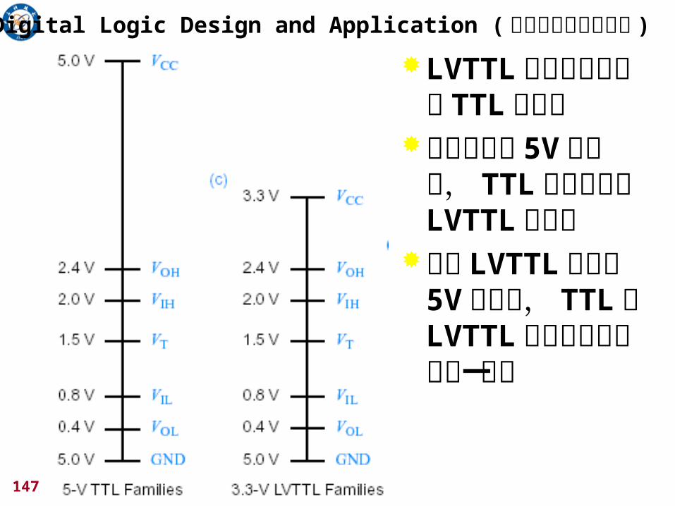
146
Digital Logic Design and Application ( 数字逻辑设计及应用 )3.9 Low-Voltage CMOS Logic and Interfacing (低电压 CMOS逻辑和接口 )
147
Digital Logic Design and Application ( 数字逻辑设计及应用 )
LVTTL输出可直接驱动 TTL输入端
如果输入是 5V容许的, TTL输出可驱动 LVTTL输入端
如果 LVTTL输出是 5V容许的, TTL和LVTTL三态输出可驱动同一总线
148
Digital Logic Design and Application ( 数字逻辑设计及应用 )
3.10.9 Emitter-Coupled Logic(发射极耦合逻辑 ECL)
How to improve speed (如何提高速度 )? —— Preventing Transistor Saturation
(防止晶体管饱和 )
Current - Mode Logic (CML,电流型逻辑 )
Or Emitter-Coupled Logic( ECL, 也称为:发射极耦合)
149
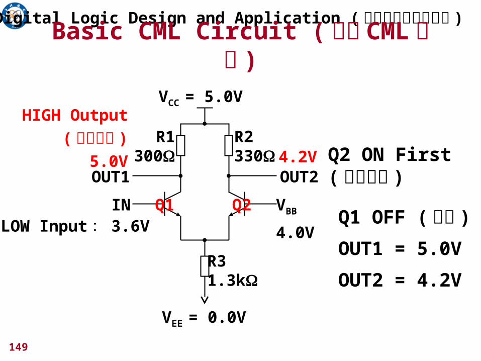
Digital Logic Design and Application ( 数字逻辑设计及应用 )
LOW Input : 3.6V
VCC = 5.0V
R1300
R2330
IN
OUT1 OUT2
VBB
4.0V
R31.3k
VEE = 0.0V
Q1 Q2
Q2 ON First( 抢先导通 )
Basic CML Circuit (基本 CML电路 )
Q1 OFF ( 截止 )
OUT1 = 5.0V
OUT2 = 4.2V
HIGH Output
( 输出高态 )5.0V 4.2V
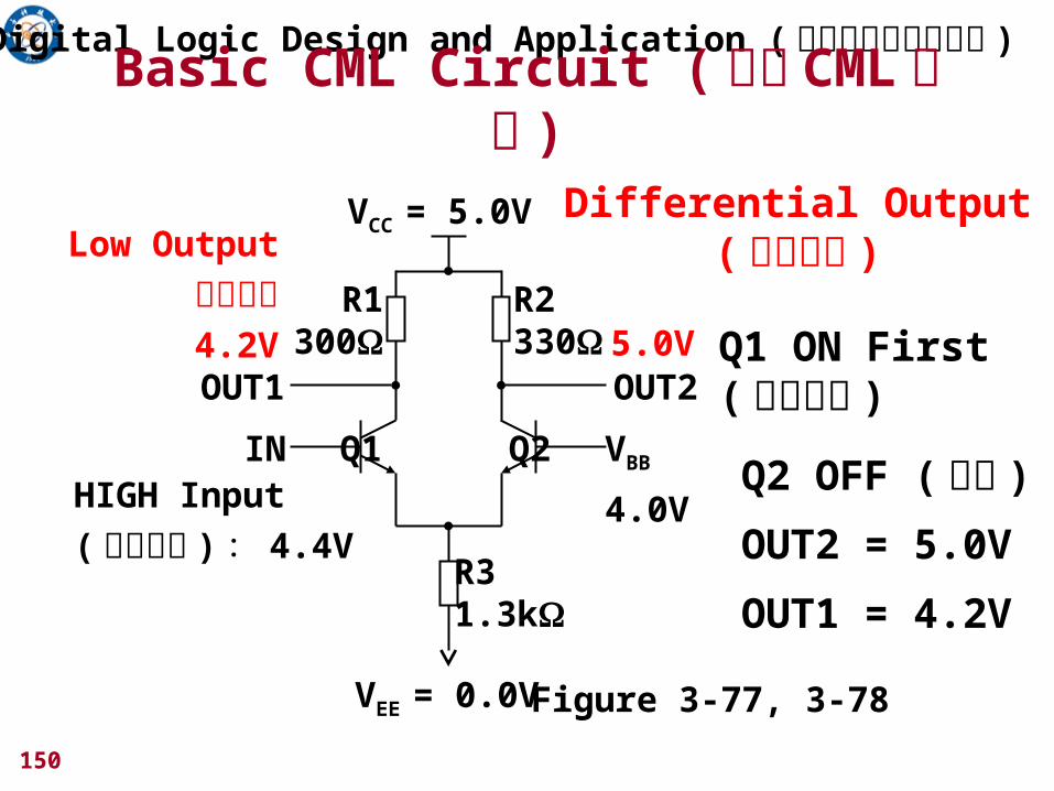
150
Digital Logic Design and Application ( 数字逻辑设计及应用 )
HIGH Input
( 输入高态 ) : 4.4V
VCC = 5.0V
R1300
R2330
IN
OUT1 OUT2
VBB
4.0V
R31.3k
VEE = 0.0V
Q1 Q2
Q1 ON First( 抢先导通 )
Q2 OFF ( 截止 )
OUT2 = 5.0V
OUT1 = 4.2V
Low Output
输出低态4.2V 5.0V
Differential Output( 差分输出 )
Basic CML Circuit (基本 CML电路 )
Figure 3-77, 3-78
151
Digital Logic Design and Application ( 数字逻辑设计及应用 )
Differential Output: Determine the Output State by Looking at the Difference between the Output Voltage rather than the Absolute Values. ( 差分输出 : 输出状态由输出电压的差值而不是由绝对值决定 )
Basic CML Circuit (基本 CML电路 )
Figure 3-77, 3-78, 3-79
Differential Input: Input circuits with Two WiresPer Logic Input. ( 差分输入 : 输入电路的每个逻辑输入端使用双线驱动。)
152
Digital Logic Design and Application ( 数字逻辑设计及应用 )
第 3 章 小结正逻辑表示和负逻辑表示三种基本逻辑运算:与、或、非
逻辑表达式、真值表、逻辑符号作为电子开关运用的二极管、双极型晶体管、 MOS场效应管的工作方式
逻辑系列: CMOS系列和 TTL系列CMOS反相器的构成及工作状态分析
153
Digital Logic Design and Application ( 数字逻辑设计及应用 )
第 3 章 小结(续)学习理解逻辑电路的静态、动态特性分析,等价的输入、输出模型 逻辑电压电平 和 噪声容限带电阻负载的电路特性、扇出非理想输入、电流尖峰和去耦电容器不用的 CMOS输入端速度、功耗
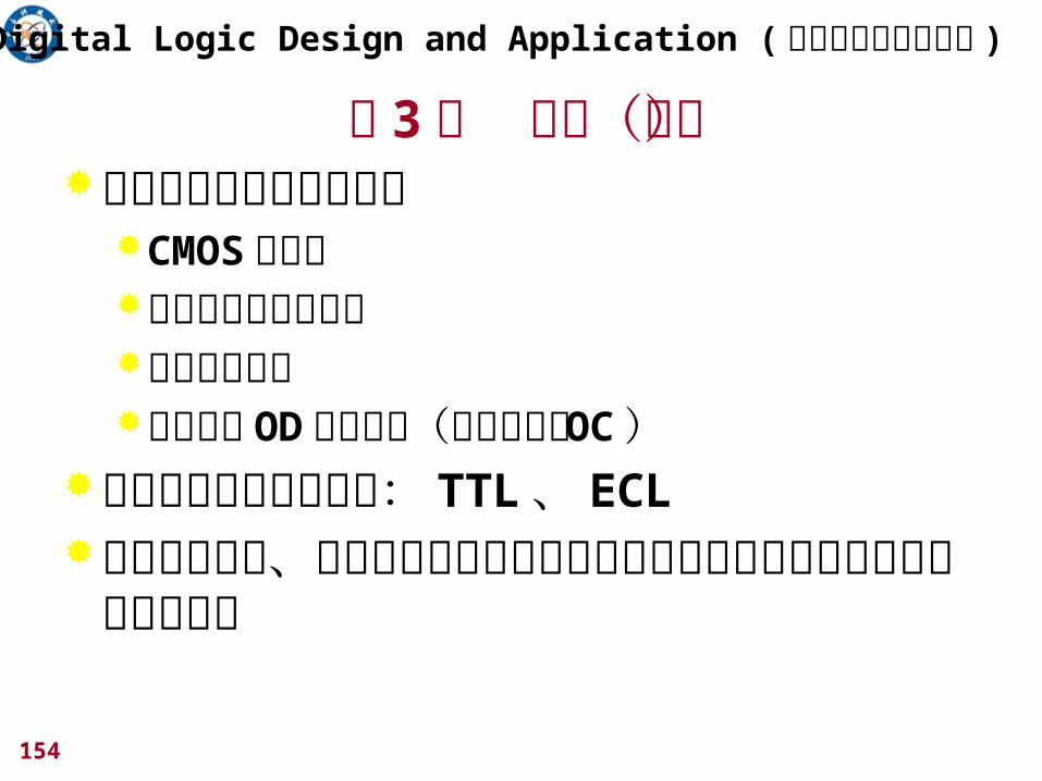
154
Digital Logic Design and Application ( 数字逻辑设计及应用 )
第 3 章 小结(续)理解特殊的输入输出结构
CMOS传输门施密特触发输入结构三态输出结构漏极开路 OD输出结构(集电极开路 OC)
了解其他类型逻辑电路: TTL、 ECL了解不同类型、不同工作电压的逻辑电路输入输出逻辑电平以及其间的连接配合
155
第 3章作业(三版) 3.1 (a) (d) (f) 3.2 (a) (d) (f) 3.5 3.9 3.14 3.23 (d) 3.36 3.92理解 3.38 3.41 3.46
计算扇出 3.49 (a) (b) 3.57 (a)
计算直流噪声容限 3.53 3.56 (c)
选做 3.61 3.62 3.81 3.28 (自学 3.5.8)
156
第 3 章作业(四版) 3.1 (a) (e) (h) 3.2 (a) (e) (h) 3.5 3.9 3.16 3.27 (d) 3.37 理解 3.39 3.42 3.47
计算扇出 3.49 (a) (b) 3.57 (a)
计算直流噪声容限 3.53 3.56 (a)
选做 3.61 3.62 3.83 3.29 (自学 3.5.7)
Digital Logic Design and Application ( 数字逻辑设计及应用 )
157
小论文 在传统半导体 Si材料中(包括教材的说法),电子与空穴的迁移率约为 2~3: 1,这种区别导致 NMOS和 PMOS在导通沟道方电阻上存在差别;若采用相同宽度制作 CMOS器件,会存在上升时间与下降时间差别,存在高电平驱动能力与低电平驱动能力差别;若采用统一驱动能力设计,则会导致与非门和或非门在逻辑面积、延迟时间等参数上的差别。
由于在超大规模数字集成中对超短沟效应和应变硅技术应用导致电子与空穴的迁移率趋于一致,在本课程中,将 2者视为相同。这样可以不用区分与非门 /或非门在逻辑面积、延迟时间等参数上的区别,也将上升时间与下降时间统一归结于信号延迟时间。
Digital Logic Design and Application ( 数字逻辑设计及应用 )
158
小论文在本课程讲解中,没有对 NMOS和 PMOS晶体管的性能进行区分。在集成度不够高时,由于电子与空穴迁移率的差别,具有相同驱动能力的PMOS器件面积可能为 NMOS器件面积的 2~3倍,而面积的变化也会导致输入 /输出电容变化,进而影响到延迟时间分析。
现根据课程教材假定为 2倍,则在采用最小设计时,仿照课程的模型,分别分析 N输入的与非门和或非门性能参数与输入端数量的关系,并得出在电路设计中具有指导意义的结论。
Digital Logic Design and Application ( 数字逻辑设计及应用 )
159
A Class Problem ( 每课一题 )
Compute the maximum fanout for a TTL output driving multiple TTL inputs. Also indicate how much “excess” driving capability is available in the LOW or HIGH state for each case.
74AS driving 74S 74AS : I(IHMAX)=20UA, I(ILMAX)=-0.5MA I(OHMAX)=-2MA,I(OLMAX)=20MA 74S : I(IHMAX)=50UA, I(ILMAX)=-2MA I(OHMAX)=-1MA,I(OLMAX)=20MA
Digital Logic Design and Application ( 数字逻辑设计及应用 )