primjena expert-choice alata i ahp metode za odabir virtex-5 fpga čipa
Implementation of a Digital Radio FrequencyMemory in a Xilinx Virtex-4 FPGA
Examensarbete utfört i elektroniksystemvid Tekniska högskolan i Linköping
av
Kristian Gustafsson
LITH-ISY-EX--05/3742--SE
Linköping 2005

Implementation of a Digital Radio FrequencyMemory in a Xilinx Virtex-4 FPGA
Examensarbete utfört i elektroniksystemvid Tekniska högskolan i Linköping
av
Kristian Gustafsson
LITH-ISY-EX--05/3742--SE
Handledare: Anna GomanSaab Bofors Dynamics AB
Anders NyhlénSaab Bofors Dynamics AB
Examinator: Kent Palmkvistisy, Linköpings Universitet
Linköping, 22 December, 2005

Avdelning, InstitutionDivision, Department
Division of Electronics SystemsDepartment of Electrical EngineeringLinköpings universitetS-581 83 Linköping, Sweden
DatumDate
2005-12-22
SpråkLanguage
� Svenska/Swedish� Engelska/English
�
�
RapporttypReport category
� Licentiatavhandling� Examensarbete� C-uppsats� D-uppsats� Övrig rapport�
�
URL för elektronisk versionhttp://www.es.isy.liu.sehttp://www.ep.liu.se/2005/3742
ISBN—
ISRNLITH-ISY-EX--05/3742--SE
Serietitel och serienummerTitle of series, numbering
ISSN—
TitelTitle
Implementation av ett digitalt radiofrekvent minne för en Xilin Virtex-4 FPGAImplementation of a Digital Radio Frequency Memory in a Xilinx Virtex-4 FPGA
FörfattareAuthor
Kristian Gustafsson
SammanfattningAbstract
Digital Radio Frequency Memory (DRFM) is a technique widely used by the de-fense industry in, for example, electronic countermeasure equipment for generatingfalse radar targets. The purpose of the DRFM technique is to use high-speed sam-pling to digitally store and recreate radio frequency and microwave signals. AtSaab Bofors Dynamics AB the technique is used, among others, in the ElectronicWarfare Simulator (ELSI). The DRFM technique is implemented in a full-customASIC circuit that has been mounted on circuit boards in ELSI. Today, the progressin the programmable hardware field has made it possible to implement the DRFMdesign in a Field Programmable Gate Array (FPGA). The FPGA technology hasmany advantages over a full custom ASIC design.
Hence, the purpose of this master’s thesis has been to develop a new DRFMdesign that can be implemented in an FPGA, using a hardware description lan-guage called VHDL. The method for this master’s thesis has been to first establisha time plan and a requirement specification. After that, a design specification hasbeen worked out based on the requirement specification. The two specificationshave served as a basis for the development of the DRFM circuit. One of therequirements on the design was that the circuit should be able to communicatethrough an external Ethernet interface. A part of the work has, thus, been toreview available external Ethernet modules on the market. The result is a DRFMdesign that has been tested through simulations. The tests shows that the designworks as described in the design specification.
NyckelordKeywords FPGA, DRFM, VHDL, Xilinx, Saab Bofors Dynamics, Mentor Graphics, Virtex-4,
Ethernet, VMEbus

AbstractDigital Radio Frequency Memory (DRFM) is a technique widely used by the de-fense industry in, for example, electronic countermeasure equipment for generatingfalse radar targets. The purpose of the DRFM technique is to use high-speed sam-pling to digitally store and recreate radio frequency and microwave signals. AtSaab Bofors Dynamics AB the technique is used, among others, in the ElectronicWarfare Simulator (ELSI). The DRFM technique is implemented in a full-customASIC circuit that has been mounted on circuit boards in ELSI. Today, the progressin the programmable hardware field has made it possible to implement the DRFMdesign in a Field Programmable Gate Array (FPGA). The FPGA technology hasmany advantages over a full custom ASIC design.
Hence, the purpose of this master’s thesis has been to develop a new DRFMdesign that can be implemented in an FPGA, using a hardware description lan-guage called VHDL. The method for this master’s thesis has been to first establisha time plan and a requirement specification. After that, a design specification hasbeen worked out based on the requirement specification. The two specificationshave served as a basis for the development of the DRFM circuit. One of therequirements on the design was that the circuit should be able to communicatethrough an external Ethernet interface. A part of the work has, thus, been toreview available external Ethernet modules on the market. The result is a DRFMdesign that has been tested through simulations. The tests shows that the designworks as described in the design specification.
v

Acknowledgements
This master’s thesis work has been carried out at Saab Bofors Dynamics ABin Linköping as a part of a Master of Science in Applied Physics and ElectricalEngineering. The result will hopefully be of great use in the Electronic WarfareSimulator at SBD. I would like to thank everyone that have helped and encouragedme during the work with this thesis. Especially, I would like to thank the followingpeople:
• Ulf Malmqvist at SBD, for giving me the opportunity to do my master’sthesis at SBD and for all help and support during my time at the company.
• My supervisor Anna Goman at SBD, for all help with the computer re-sources, software and the VHDL coding.
• Anders Nyhlén, my second supervisor at SBD, for all the time he has spenton explaining the complex systems in ELSI for me and for all support given.
• Sture Carlson at SBD, for the detailed review of my thesis report and for allhelp with litterateurs used for the technology chapter of this report.
• Leif Tranell at SBD, for all the support with troublesome software.
• My opponent Oskar Ståhl for his valuable comments and feedback on mythesis report.
• My examiner Kent Palmkvist at the Division of Electronics Systems, De-pertment of Electrical Engineering at Linköping University for valuable com-ments on the report.
vii

List of Acronyms
A/D Analog to DigitalADC A/D ConverterASIC Application Specific CircuitASMBL Advanced Silicon Modular BlockBRAM Block RAMCLB Configurable Logic BlockCMOS Complementary Metal-Oxide SemiconductorCSMA/CD Carrier Sense Multiple Access with Collision DetectionCW Continuous WaveD/A Digital to AnalogDAC D/A ConverterDCM Digital Clock ManagerDIX Digital Intel XeroxDRFM Digital Radio Frequency MemoryDSP Digital Signal ProcessingECM Electronic CountermeasureELSI Electronic Warfare SimulatorFPGA Field Programmable Gate ArrayFSM Finite State MachineGPIO General Purpose Input/OutputHSD High-Speed DataHSDE High-Speed Data EnhancedHWIL Hardware-in-the-loopIC Integrated CircuitIF Intermediate FrequencyIEEE Institute of Electrical and Electronics EngineersIOB Input/Output BlockIP Intellectual PropertyIP Internet ProtocolLAN/MAN Local and Metropolitan Area NetworkLiU Linköping UniversityLUT Look-Up TableLVDS Low Voltage Differential Signaling
x
MAC Media Access ControlMDI Media Dependent InterfaceMII Media Independent InterfaceOUI Organizationally Unique IdentifierPAR Place and RoutePHY Physical LayerPRF Pulse Repetition FrequencyRAM Random-Access MemoryRF Radio FrequencySBD Saab Bofors Dynamics ABSLOS Synthetic Line of SightSoC Software-on-ChipTCP Transmission ProtocolTEG Target Echo GeneratorUDP User Datagram ProtocolUUT Unit Under TestVHDL VHSIC Hardware Description LanguageVHSIC Very High Speed Integrated CircuitVME VersaModule Eurocard
Contents
1 Introduction 11.1 Background . . . . . . . . . . . . . . . . . . . . . . . . . . . . . . . 11.2 Purpose . . . . . . . . . . . . . . . . . . . . . . . . . . . . . . . . . 21.3 Method . . . . . . . . . . . . . . . . . . . . . . . . . . . . . . . . . 21.4 Limitations . . . . . . . . . . . . . . . . . . . . . . . . . . . . . . . 31.5 Thesis outline . . . . . . . . . . . . . . . . . . . . . . . . . . . . . . 3
2 Technology & Background 52.1 Saab Bofors Dynamics AB . . . . . . . . . . . . . . . . . . . . . . . 52.2 Radar seekers . . . . . . . . . . . . . . . . . . . . . . . . . . . . . . 62.3 Electronic countermeasures . . . . . . . . . . . . . . . . . . . . . . 62.4 Digital Radio Frequency Memory . . . . . . . . . . . . . . . . . . . 72.5 The Electronic Warfare Simulator . . . . . . . . . . . . . . . . . . . 72.6 The Target Echo Generator . . . . . . . . . . . . . . . . . . . . . . 102.7 The current DRFM circuit . . . . . . . . . . . . . . . . . . . . . . . 10
2.7.1 The function of the DRFM . . . . . . . . . . . . . . . . . . 112.8 The new DRFM circuit . . . . . . . . . . . . . . . . . . . . . . . . 132.9 Field Programmable Gate Array . . . . . . . . . . . . . . . . . . . 142.10 Choosing the FPGA circuit . . . . . . . . . . . . . . . . . . . . . . 152.11 The Virtex-4 family . . . . . . . . . . . . . . . . . . . . . . . . . . 15
2.11.1 Hardware resources in Virtex-4 . . . . . . . . . . . . . . . . 162.11.2 Intellectual Property blocks . . . . . . . . . . . . . . . . . . 192.11.3 Xilinx CORE generator . . . . . . . . . . . . . . . . . . . . 20
2.12 Communication . . . . . . . . . . . . . . . . . . . . . . . . . . . . . 202.12.1 VMEbus . . . . . . . . . . . . . . . . . . . . . . . . . . . . . 212.12.2 Ethernet . . . . . . . . . . . . . . . . . . . . . . . . . . . . . 212.12.3 The Internet protocol suite . . . . . . . . . . . . . . . . . . 232.12.4 Choosing communication interface . . . . . . . . . . . . . . 23
2.13 Choosing Ethernet interface . . . . . . . . . . . . . . . . . . . . . . 242.13.1 The choice of Ethernet module . . . . . . . . . . . . . . . . 26
3 Implementation & Testing 293.1 Layout decisions . . . . . . . . . . . . . . . . . . . . . . . . . . . . 29
3.1.1 The memory . . . . . . . . . . . . . . . . . . . . . . . . . . 29
xi
xii Contents
3.1.2 The interface . . . . . . . . . . . . . . . . . . . . . . . . . . 303.2 The design flow . . . . . . . . . . . . . . . . . . . . . . . . . . . . . 303.3 Tools . . . . . . . . . . . . . . . . . . . . . . . . . . . . . . . . . . . 323.4 The DRFM design . . . . . . . . . . . . . . . . . . . . . . . . . . . 33
3.4.1 Inputs and outputs . . . . . . . . . . . . . . . . . . . . . . . 343.4.2 The control logic block . . . . . . . . . . . . . . . . . . . . . 353.4.3 The DRFM memory . . . . . . . . . . . . . . . . . . . . . . 383.4.4 The external interface . . . . . . . . . . . . . . . . . . . . . 383.4.5 Other resources . . . . . . . . . . . . . . . . . . . . . . . . . 40
3.5 Testing methodology . . . . . . . . . . . . . . . . . . . . . . . . . . 40
4 Results & Discussion 434.1 Results . . . . . . . . . . . . . . . . . . . . . . . . . . . . . . . . . . 43
4.1.1 Cases tested through simulation . . . . . . . . . . . . . . . 434.2 Performance . . . . . . . . . . . . . . . . . . . . . . . . . . . . . . . 454.3 Difficulties . . . . . . . . . . . . . . . . . . . . . . . . . . . . . . . . 45
5 Conclusions & Future work 475.1 Conclusions . . . . . . . . . . . . . . . . . . . . . . . . . . . . . . . 475.2 Future work . . . . . . . . . . . . . . . . . . . . . . . . . . . . . . . 48
5.2.1 Improvement of the design . . . . . . . . . . . . . . . . . . 485.2.2 The DRFM circuit board . . . . . . . . . . . . . . . . . . . 48
Bibliography 51
A Time Plan 53
B Requirement Specification 54
C Design Specification 63
D Test Wave Forms 77
Contents xiii
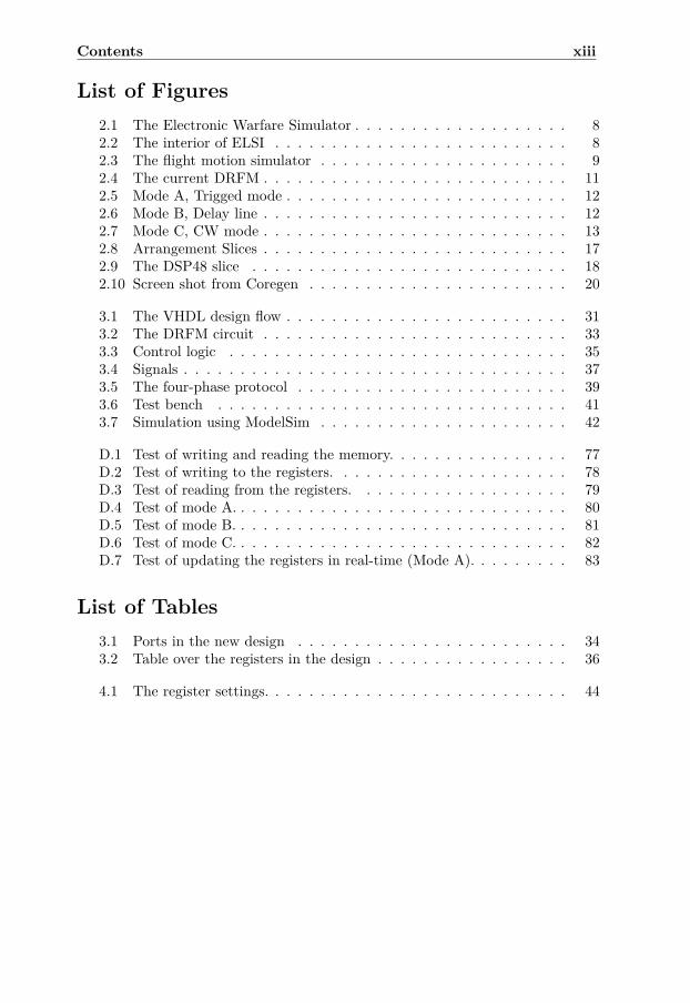
List of Figures2.1 The Electronic Warfare Simulator . . . . . . . . . . . . . . . . . . . 82.2 The interior of ELSI . . . . . . . . . . . . . . . . . . . . . . . . . . 82.3 The flight motion simulator . . . . . . . . . . . . . . . . . . . . . . 92.4 The current DRFM . . . . . . . . . . . . . . . . . . . . . . . . . . . 112.5 Mode A, Trigged mode . . . . . . . . . . . . . . . . . . . . . . . . . 122.6 Mode B, Delay line . . . . . . . . . . . . . . . . . . . . . . . . . . . 122.7 Mode C, CW mode . . . . . . . . . . . . . . . . . . . . . . . . . . . 132.8 Arrangement Slices . . . . . . . . . . . . . . . . . . . . . . . . . . . 172.9 The DSP48 slice . . . . . . . . . . . . . . . . . . . . . . . . . . . . 182.10 Screen shot from Coregen . . . . . . . . . . . . . . . . . . . . . . . 20
3.1 The VHDL design flow . . . . . . . . . . . . . . . . . . . . . . . . . 313.2 The DRFM circuit . . . . . . . . . . . . . . . . . . . . . . . . . . . 333.3 Control logic . . . . . . . . . . . . . . . . . . . . . . . . . . . . . . 353.4 Signals . . . . . . . . . . . . . . . . . . . . . . . . . . . . . . . . . . 373.5 The four-phase protocol . . . . . . . . . . . . . . . . . . . . . . . . 393.6 Test bench . . . . . . . . . . . . . . . . . . . . . . . . . . . . . . . 413.7 Simulation using ModelSim . . . . . . . . . . . . . . . . . . . . . . 42
D.1 Test of writing and reading the memory. . . . . . . . . . . . . . . . 77D.2 Test of writing to the registers. . . . . . . . . . . . . . . . . . . . . 78D.3 Test of reading from the registers. . . . . . . . . . . . . . . . . . . 79D.4 Test of mode A. . . . . . . . . . . . . . . . . . . . . . . . . . . . . . 80D.5 Test of mode B. . . . . . . . . . . . . . . . . . . . . . . . . . . . . . 81D.6 Test of mode C. . . . . . . . . . . . . . . . . . . . . . . . . . . . . . 82D.7 Test of updating the registers in real-time (Mode A). . . . . . . . . 83
List of Tables3.1 Ports in the new design . . . . . . . . . . . . . . . . . . . . . . . . 343.2 Table over the registers in the design . . . . . . . . . . . . . . . . . 36
4.1 The register settings. . . . . . . . . . . . . . . . . . . . . . . . . . . 44

xiv Contents
Chapter 1
Introduction
This chapter serves as an introduction to this master’s thesis. It starts with de-scribing the background to why this project was initiated. After that the purposeof the master’s thesis is described and the chapter ends with a description of themethod used and the limitations of the thesis.
1.1 BackgroundThe Electronic Warfare Simulator, ELSI, is situated at Saab Bofors Dynamics AB(SBD) in Linköping. ELSI is used to test and verify radar seekers capabilitiesagainst simulated scenarios of targets and countermeasures [1] . The simulatoris depending on a huge amount of advanced hardware. To be able to broadenthe type of seekers that can be tested and to meet upcoming new demands thefacility is undergoing a constant upgrading. One part of the equipment needed tobe upgraded is a Digital Radio Frequency Memory (DRFM) circuit. The originalDRFM circuit is a full custom Application Specific Integrated Circuit (ASIC)design developed at SBD in the early 90’s. The circuit is running at 200 MHz, avery fast circuit at the time. Due to the technical development in programmablehardware field, a new DRFM circuit should be possible to develop using FPGAtechnology instead of ASIC.
Field Programmable Gate Arrays (FPGAs) have undergone a major transitionthe last few years: From being small basic programmable logic hardware, to thenewest FPGAs, being large circuits, with transistor count equivalent to the newestPC processors and having advanced integrated logic such as embedded processorsand Ethernet capabilities. Designs, earlier only possible to implement as an ASIC,can now be implemented in a single FPGA. There are still benefits of developingASICs due to the small chip size, low power consumption and very low chip costsper unit when a large amount of units have to be manufactured. The disadvan-tages are the long design time of ASICs, the difficulty to alter the design aftermanufacturing and the expensive development cost when only a small series ofchips are needed. Using FPGAs on the other hand, the design can quickly bealtered and tested during the development. When only a few chips are needed an
1
2 Introduction
FPGA solution will be very cheap, both in time and cost, in comparison to anASIC solution. This is why a solution using an FPGA has been chosen by SBD.
This master’s degree thesis has been performed in the form of a project, i.e.setting up a time plan and writing a requirement specification as well as a designspecification. The idea was to use a working method similar to the methods usedat high-tech companies such as SBD. Essential was to secure control of the cost,i.e. spent time, of the project and to be able to supervise the progress of thedevelopment of the DRFM circuit.
The thesis work has been carried out in accordance with the requirementsof the Master of Science degree at Linköping University (LiU) in Sweden. Theexamination has been done by assistant professor Kent Palmkvist at the divisionof Electronics Systems, a part of the Department of Electrical Engineering at LiU.
1.2 PurposeThe main objective of the project was to develop a DRFM circuit to be used inthe ELSI simulator. The DRFM functions should be implemented in an FPGAusing VHDL as the hardware description language for programming the logic. TheDRFM should be controlled by a computer. The interface was at first chosen bySBD to be a standard VMEbus interface but during the project the interface waschanged to be an Ethernet interface instead, see Section 2.12. No requirementsregarding the component cost of the FPGA were made.
To be able to fulfill the objectives above, the folowing tasks had to be accom-plished:
• A survey of FPGAs suitable for the project.
• Study of the design of the VMEbus.
• Study of the Ethernet standard and a market survey of available Ethernetmodules.
• Review of the available development tools at SBD to be able choose the besttools for the development of the circuit.
• Development of the DRFM circuit using VHDL.
1.3 MethodThe first task of this project was to establish a time plan for the entire project.The time plan can be found in Appendix A. The time plan was used to estimatethe time needed for the different phases of the project.
The second task was to study the documentation of the DRFM circuit usedtoday. After having established an overview of the function and capability of thepresent circuit a design requirement specification was composed in collaborationwith the ELSI staff at SBD. The specification can be viewed in Appendix B.
1.4 Limitations 3
The third task was to study design alternatives in more detail, i.e. the choiceof the FPGA circuit, the layout of the design, the development tools to be usedetc. This ended up in a design specification, available as Appendix C.
After the three first steps of the project the actual development started. Thisincluded learning the chosen development tools, VHDL programming, behavioralsimulation of the design, synthesis, design implementation and testing the designthrough timing simulation. This step was the major part of the project in termsof time. After the functionality of the design had been verified the circuit wasconsidered complete. No test in hardware was performed, as the hardware platformto be used for the DRFM circuit had not been developed at the time for this thesisproject. Hence, hardware tests had not been included in the time plan.
1.4 LimitationsThis thesis project was completed in accordance with the regulation of thesisprojects at Linköping University. Due to the limitation in time, the goal of thisproject has been to develop the architecture and functions of the new DRFMcircuit. The communication interface and testing of the logic in hardware havenot been part of the project.
1.5 Thesis outlineChapter 2, Technology & Background, is intended to give the reader the back-ground information needed to understand the implementation of the DRFM de-sign.
Chapter 3, Implementation & Testing, describes layout decisions made, the imple-mentation flow used and the implemented design. A discussion is also held aroundthe testing methods.
Chapter 4, Results & Discussion, presents the result of the master’s thesis anda discussion around the difficulties that have come up during the thesis work.
Chapter 5, Conclusions & Future work, discusses the conclusions that can bemade and future improvements that can be done.
The appendices contains the time plan, the requirement specification, the designspecification and wave forms from simulations of the design.

4 Introduction
Chapter 2
Technology & Background
This chapter is intended to give the reader the background information required tounderstand the implementation of the DRFM circuit. The chapter starts with adescription of the company where this thesis project has been performed. It con-tinues with a short technology background of radar seekers, electronic countermea-sures and the DRFM technology. After that, the simulator ELSI will be describedin more detail. In particular the DRFM circuit used today and the requirements ofthe new architecture will be explained. Furthermore the different technologies andlogic blocks needed to implement the design will be described. The chapter endswith a description and a discussion of the communication interface of the DRFMcircuit.
2.1 Saab Bofors Dynamics AB
Saab Bofors Dynamics AB (SBD) is a business unit within Saab AB having ap-proximately 1200 employees. The head quarter is located in Karlskoga, but localdivisions are also situated in Linköping, Eskilstuna, Gothenburg and Stockholm.SBD develops, markets and produces missile systems and man-portable supportweapons. The products are aimed for use at both land, air and above and underwater. SBD has customers all over the world, approximately 80% of the company’sturnover comes from export, but the Swedish market is still an important base forthe company. SBD participates in a number of international collaborations and hasalso developed own defense products. Well-know, entirely own-developed, prod-ucts are the anti-ship missile RBS 15, the anti-aircraft missile system BAMSE andthe recoilless gun system Carl Gustaf1.
1Carl Gustaf is well-known for its appearance in the Steven Spielberg Hollywood movie “Warof the Worlds” in 2005
5
6 Technology & Background
2.2 Radar seekersIn the Electronic Warfare Simulator, ELSI, the accuracy and performance of radarseekers in guided missiles are tested. A guided missile is made up of a series ofdifferent parts. These are used in applications such as propulsion, control andguidance. The guidance of the missile is controlled by the guidance computer.It maneuvers the missile during the flight towards the target pointed out by theradar seeker.
A basic radar consists of a radio transmitter, a radio receiver, two antennasand signal-processing circuitry. The radio transmitter sends radio waves, i.e. elec-tromagnetic waves, which radiates from the transmitter antenna. The receiveruses the other antenna to pick up echoes of the waves that have been reflected on,hopefully, the wanted target. These echoes are forwarded to the signal-processingcircuitry that calculates for example the distance and the direction to the target.As the radio waves travel at constant speed, the speed of light, the distance ispossible to calculate according to the formula in example 2.1.
Example 2.1: Target distance formula.
R =12
T c
R is the target distance in metersT is the round-trip time in secondsc is the speed of light in m/s[2]
To avoid the transmitter from interfering with the receiver the transmitter usuallysends the radio waves in pulses and the receiver is turned off during transmission.The rate at which the transmitter sends pulses is called pulse repetition frequency,PRF.
In practice the radar seeker uses only one antenna for both transmitting andreceiving waves. In this case the antenna is shared by time multiplexing.
The antenna concentrates the energy dissipated in a narrow beam to be ableto more precisely detect targets. Due to the narrow area of detection, the beamhas to be swept over the region of interest to be able to find the wanted targets.[2]
2.3 Electronic countermeasuresTo avoid being hit by a missile the target, e.g. a fighter jet, can use electroniccountermeasures (ECM) to trick the missile. There is a wide variety of ECMtechniques that can be used depending on the situation. The simplest example iswhen an airborne target deploys chaff in the air to confuse the missile. Chaff aresmall strips of metal or metal-coated dielectric fibers with an optimal length of halfof that of the radar signal wave length. A huge amount of these are deployed inthe air and can stay there for a long time producing strong radar echoes hopefully
2.4 Digital Radio Frequency Memory 7
misleading the missile. Other examples are noise jamming and false targets. Noisejamming is intended to increase the background noise making it more difficult tolocate the targets. False targets can be generated in different ways. The simplestway is to use a transponder which receives the pulse, waits for a certain delay,corresponding to the additional target range, and transmits the pulse back to theseeker. The transmitted false target pulse is hopefully interpreted by the radarseeker as target situated on a certain distance from the real target. To producemore realistic false targets a repeater can be used. The repeater is similar to thetransponder but is also equipped with a memory. The memory can be used tostore the intercepted radar pulses and using them to display multiple and movingtargets on different ranges and velocities for the seeker. To be able to fully exploitthis principle a digital radio frequency memory (DRFM) could be used.[2]
2.4 Digital Radio Frequency MemoryDigital radio frequency memory, DRFM, is a technique used for storing and recre-ating radio frequency (RF) and microwave signals. The principle of the DRFMwas invented in 1974 at EMI Electronics Ltd in Britain. The basic task is to inputan RF signal that has been converted to a frequency low enough to be sampled bya high-speed A/D converter (ADC). The sampled signal is stored in a high-speedmemory and can be retrieved and converted back to the original signal using aD/A converter (DAC). A simplification of the DRFM function is to see the DRFMas a variable delay line for radio frequency signals. The technique is often usedin electronic warfare applications. In particular DRFMs are widely used in ECMproducts to generate false radar echoes. SBD markets military products usingthe DRFM technique, but the technique is also used in the Electronic WarfareSimulator at SBD.[3]
2.5 The Electronic Warfare SimulatorThe Electronic Warfare Simulator (ELSI) is a hardware-in-the-loop, HWIL, sim-ulator used to test radar seekers. An HWIL simulator uses an actual individualof the seeker that is presented with a complete simulated target scenario. This isused to verify and test the radar seeker capabilities against simulated scenarios oftargets and countermeasures. By using ELSI, different conditions and propertiesof the environment can be simulated (e.g. weather conditions, seeker primings,target behavior, ECM)[1]
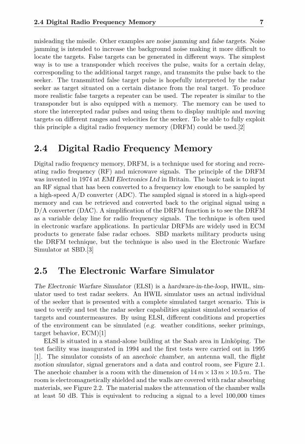
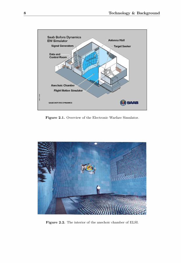
ELSI is situated in a stand-alone building at the Saab area in Linköping. Thetest facility was inaugurated in 1994 and the first tests were carried out in 1995[1]. The simulator consists of an anechoic chamber, an antenna wall, the flightmotion simulator, signal generators and a data and control room, see Figure 2.1.The anechoic chamber is a room with the dimension of 14 m× 13 m× 10.5 m. Theroom is electromagnetically shielded and the walls are covered with radar absorbingmaterials, see Figure 2.2. The material makes the attenuation of the chamber wallsat least 50 dB. This is equivalent to reducing a signal to a level 100,000 times
8 Technology & Background
Figure 2.1. Overview of the Electronic Warfare Simulator.
Figure 2.2. The interior of the anechoic chamber of ELSI.
2.5 The Electronic Warfare Simulator 9
weaker than its original strength. The high attenuation is a requirement to makethe walls invisible to the seeker, instead it just sees the target scenario presentedby the simulator.
On one of the walls of the chamber 16 radar antennas and transmitters aresituated. These are used by the simulator to simulate and present the targetscenario for the seeker. The antenna wall is mounted on a framework which ismounted on a concrete foundation. The antennas are placed on a horizontal rowwith one degrees spacing on a segment of a circle with a radius of 13 meters. Thecircle has the origin at the axis intersection of the gimbals of the flight motionsimulator which is situated on the opposite wall.
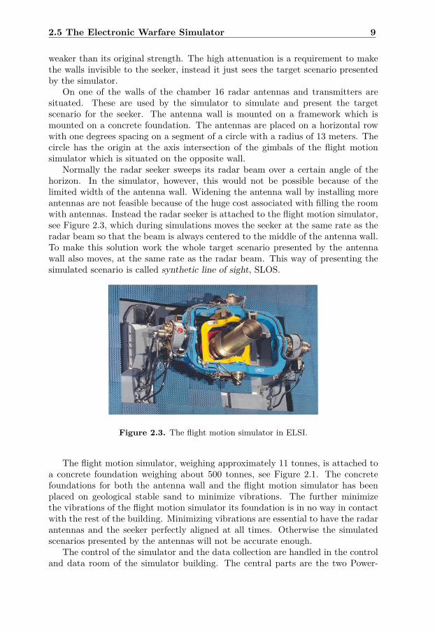
Normally the radar seeker sweeps its radar beam over a certain angle of thehorizon. In the simulator, however, this would not be possible because of thelimited width of the antenna wall. Widening the antenna wall by installing moreantennas are not feasible because of the huge cost associated with filling the roomwith antennas. Instead the radar seeker is attached to the flight motion simulator,see Figure 2.3, which during simulations moves the seeker at the same rate as theradar beam so that the beam is always centered to the middle of the antenna wall.To make this solution work the whole target scenario presented by the antennawall also moves, at the same rate as the radar beam. This way of presenting thesimulated scenario is called synthetic line of sight, SLOS.
Figure 2.3. The flight motion simulator in ELSI.
The flight motion simulator, weighing approximately 11 tonnes, is attached toa concrete foundation weighing about 500 tonnes, see Figure 2.1. The concretefoundations for both the antenna wall and the flight motion simulator has beenplaced on geological stable sand to minimize vibrations. The further minimizethe vibrations of the flight motion simulator its foundation is in no way in contactwith the rest of the building. Minimizing vibrations are essential to have the radarantennas and the seeker perfectly aligned at all times. Otherwise the simulatedscenarios presented by the antennas will not be accurate enough.
The control of the simulator and the data collection are handled in the controland data room of the simulator building. The central parts are the two Power-
10 Technology & Background
Hawk 740 computers developed by the American company Concurrent ComputerCorporation2. The two simulation computers updates the hardware with data inreal-time during test runs.
The last part of ELSI is the signal generators. These contain different equip-ment which handles the transmission of the complete simulation scenario to theantennas. For this master’s thesis the most interesting equipment of the signalgenerators are the Target Echo Generator (TEG).[1]
2.6 The Target Echo GeneratorThe TEG is the part of the signal generators that this thesis is all about. Moreprecisely, focus is on the DRFM circuits situated on four circuit boards in theTEG. These circuit boards have two main functions:
1. Store target echoes.
2. Control the delay of the echoes during run-time.
The delays of the echoes are introduced to be able to simulate the distance toa target. Normally the distance to the target can be several kilometers but inthe anechoic chamber of ELSI there is merely 13 meters between the seeker andthe antennas. Therefore the echoes are delayed to simulate the distance. Thisis possible since the delay is equivalent to distance according to the formula inexample 2.1.
The four DRFM circuit boards are mounted in a VME chassie together withother circuit boards used for generation of different trigger signals. The VMEchassie, see Section 2.12.1, has a custom made backplane that has been developedat Saab. The backplane is used for external communication and power.
The DRFM circuit boards consist mainly of a DRFM circuit and an A/Dconverter. Each of them generates echoes for one target during simulation. Hence,four targets can be displayed at the same time during run-time. The function ofthe DRFM circuits will be described in more detail in Section 2.7.
The circuit boards are controlled through an interface called High-Speed DataEnhanced (HSDE) interface. The HSD bus is an industry de facto standard de-veloped by Encore3. This interface is used to load pulses to the memory in theDRFM circuits and to control the delays during run-time.
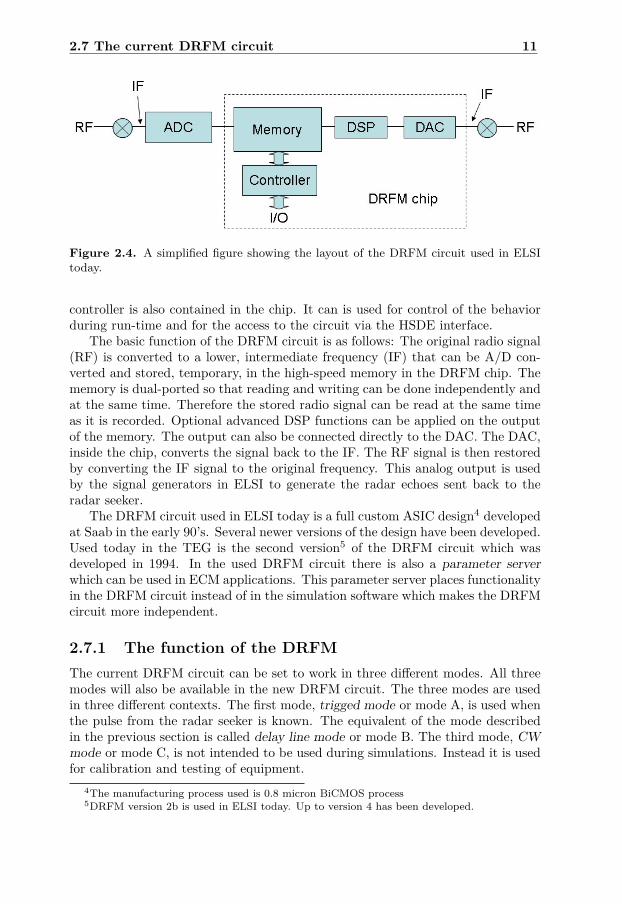
2.7 The current DRFM circuitThere are several different architectures that could be used to implement a DRFMchip [3]. The architecture used in the current ELSI DRFM is illustrated in Fig-ure 2.4. It consists of a high-speed memory, DSP logic and an integrated DAC. A
2Concurrent Computer Corporation is a company specialized in real-time computer systemsfor industry and government, see http://www.ccur.com
3Encore is a real-time computing company which was acquired by Compro in 2002, seehttp://www.encore.com
2.7 The current DRFM circuit 11
Figure 2.4. A simplified figure showing the layout of the DRFM circuit used in ELSItoday.
controller is also contained in the chip. It can is used for control of the behaviorduring run-time and for the access to the circuit via the HSDE interface.
The basic function of the DRFM circuit is as follows: The original radio signal(RF) is converted to a lower, intermediate frequency (IF) that can be A/D con-verted and stored, temporary, in the high-speed memory in the DRFM chip. Thememory is dual-ported so that reading and writing can be done independently andat the same time. Therefore the stored radio signal can be read at the same timeas it is recorded. Optional advanced DSP functions can be applied on the outputof the memory. The output can also be connected directly to the DAC. The DAC,inside the chip, converts the signal back to the IF. The RF signal is then restoredby converting the IF signal to the original frequency. This analog output is usedby the signal generators in ELSI to generate the radar echoes sent back to theradar seeker.
The DRFM circuit used in ELSI today is a full custom ASIC design4 developedat Saab in the early 90’s. Several newer versions of the design have been developed.Used today in the TEG is the second version5 of the DRFM circuit which wasdeveloped in 1994. In the used DRFM circuit there is also a parameter serverwhich can be used in ECM applications. This parameter server places functionalityin the DRFM circuit instead of in the simulation software which makes the DRFMcircuit more independent.
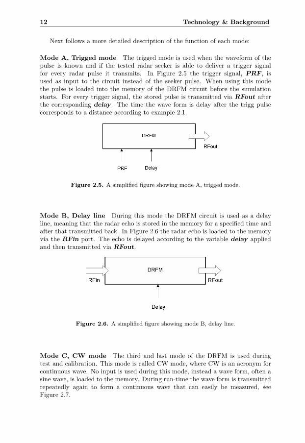
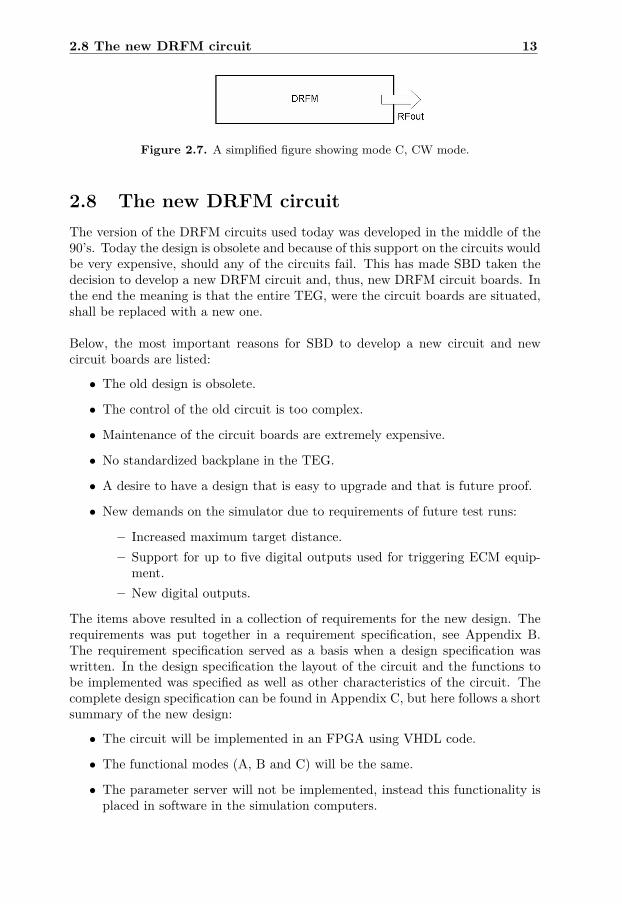
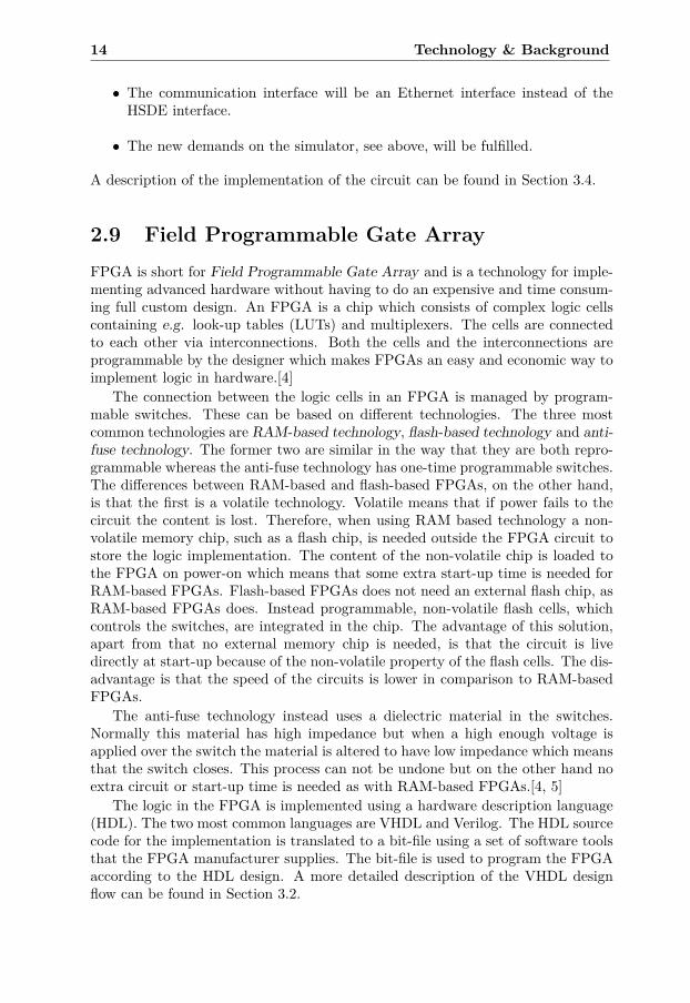
2.7.1 The function of the DRFMThe current DRFM circuit can be set to work in three different modes. All threemodes will also be available in the new DRFM circuit. The three modes are usedin three different contexts. The first mode, trigged mode or mode A, is used whenthe pulse from the radar seeker is known. The equivalent of the mode describedin the previous section is called delay line mode or mode B. The third mode, CWmode or mode C, is not intended to be used during simulations. Instead it is usedfor calibration and testing of equipment.
4The manufacturing process used is 0.8 micron BiCMOS process5DRFM version 2b is used in ELSI today. Up to version 4 has been developed.
12 Technology & Background
Next follows a more detailed description of the function of each mode:
Mode A, Trigged mode The trigged mode is used when the waveform of thepulse is known and if the tested radar seeker is able to deliver a trigger signalfor every radar pulse it transmits. In Figure 2.5 the trigger signal, PRF, isused as input to the circuit instead of the seeker pulse. When using this modethe pulse is loaded into the memory of the DRFM circuit before the simulationstarts. For every trigger signal, the stored pulse is transmitted via RFout afterthe corresponding delay. The time the wave form is delay after the trigg pulsecorresponds to a distance according to example 2.1.
Figure 2.5. A simplified figure showing mode A, trigged mode.
Mode B, Delay line During this mode the DRFM circuit is used as a delayline, meaning that the radar echo is stored in the memory for a specified time andafter that transmitted back. In Figure 2.6 the radar echo is loaded to the memoryvia the RFin port. The echo is delayed according to the variable delay appliedand then transmitted via RFout.
Figure 2.6. A simplified figure showing mode B, delay line.
Mode C, CW mode The third and last mode of the DRFM is used duringtest and calibration. This mode is called CW mode, where CW is an acronym forcontinuous wave. No input is used during this mode, instead a wave form, often asine wave, is loaded to the memory. During run-time the wave form is transmittedrepeatedly again to form a continuous wave that can easily be measured, seeFigure 2.7.
2.8 The new DRFM circuit 13
Figure 2.7. A simplified figure showing mode C, CW mode.
2.8 The new DRFM circuitThe version of the DRFM circuits used today was developed in the middle of the90’s. Today the design is obsolete and because of this support on the circuits wouldbe very expensive, should any of the circuits fail. This has made SBD taken thedecision to develop a new DRFM circuit and, thus, new DRFM circuit boards. Inthe end the meaning is that the entire TEG, were the circuit boards are situated,shall be replaced with a new one.
Below, the most important reasons for SBD to develop a new circuit and newcircuit boards are listed:
• The old design is obsolete.
• The control of the old circuit is too complex.
• Maintenance of the circuit boards are extremely expensive.
• No standardized backplane in the TEG.
• A desire to have a design that is easy to upgrade and that is future proof.
• New demands on the simulator due to requirements of future test runs:
– Increased maximum target distance.– Support for up to five digital outputs used for triggering ECM equip-
ment.– New digital outputs.
The items above resulted in a collection of requirements for the new design. Therequirements was put together in a requirement specification, see Appendix B.The requirement specification served as a basis when a design specification waswritten. In the design specification the layout of the circuit and the functions tobe implemented was specified as well as other characteristics of the circuit. Thecomplete design specification can be found in Appendix C, but here follows a shortsummary of the new design:
• The circuit will be implemented in an FPGA using VHDL code.
• The functional modes (A, B and C) will be the same.
• The parameter server will not be implemented, instead this functionality isplaced in software in the simulation computers.
14 Technology & Background
• The communication interface will be an Ethernet interface instead of theHSDE interface.
• The new demands on the simulator, see above, will be fulfilled.
A description of the implementation of the circuit can be found in Section 3.4.
2.9 Field Programmable Gate ArrayFPGA is short for Field Programmable Gate Array and is a technology for imple-menting advanced hardware without having to do an expensive and time consum-ing full custom design. An FPGA is a chip which consists of complex logic cellscontaining e.g. look-up tables (LUTs) and multiplexers. The cells are connectedto each other via interconnections. Both the cells and the interconnections areprogrammable by the designer which makes FPGAs an easy and economic way toimplement logic in hardware.[4]
The connection between the logic cells in an FPGA is managed by program-mable switches. These can be based on different technologies. The three mostcommon technologies are RAM-based technology, flash-based technology and anti-fuse technology. The former two are similar in the way that they are both repro-grammable whereas the anti-fuse technology has one-time programmable switches.The differences between RAM-based and flash-based FPGAs, on the other hand,is that the first is a volatile technology. Volatile means that if power fails to thecircuit the content is lost. Therefore, when using RAM based technology a non-volatile memory chip, such as a flash chip, is needed outside the FPGA circuit tostore the logic implementation. The content of the non-volatile chip is loaded tothe FPGA on power-on which means that some extra start-up time is needed forRAM-based FPGAs. Flash-based FPGAs does not need an external flash chip, asRAM-based FPGAs does. Instead programmable, non-volatile flash cells, whichcontrols the switches, are integrated in the chip. The advantage of this solution,apart from that no external memory chip is needed, is that the circuit is livedirectly at start-up because of the non-volatile property of the flash cells. The dis-advantage is that the speed of the circuits is lower in comparison to RAM-basedFPGAs.
The anti-fuse technology instead uses a dielectric material in the switches.Normally this material has high impedance but when a high enough voltage isapplied over the switch the material is altered to have low impedance which meansthat the switch closes. This process can not be undone but on the other hand noextra circuit or start-up time is needed as with RAM-based FPGAs.[4, 5]
The logic in the FPGA is implemented using a hardware description language(HDL). The two most common languages are VHDL and Verilog. The HDL sourcecode for the implementation is translated to a bit-file using a set of software toolsthat the FPGA manufacturer supplies. The bit-file is used to program the FPGAaccording to the HDL design. A more detailed description of the VHDL designflow can be found in Section 3.2.
2.10 Choosing the FPGA circuit 15
2.10 Choosing the FPGA circuitThe prerequisite of this project was that the design should be possible to implementin an FPGA. This was a demand by SBD and the reason for that was that SBDwanted to be able to more easily change the design if needed in the future. Thefirst task was thus to choose an FPGA for the implementation. The division ofSBD where this project has been carried out has a lot of experience of using theActel FPGAs. Hence it would have been a natural decision to use one of theircircuits. The disadvantage with the Actel FPGAs is that Actel uses the anti-fuseswitch technology in their FPGAs, a technology that does not match the demandof a design that is easy to update. The author of this report, however, has alot of experience of Xilinx FPGAs, which has a RAM-based switch technology.Therefore the Xilinx FGPAs were more closely studied to be able to differentiatethe FPGA needed. First of all a decision had to be made as of what classificationthe FPGA should have. There are different circuit classifications which specify thecondition of the environment (temperature, radiation etc.) that the circuit can beused in. Due to the fact that the circuit will be used in a computer server roomthat is air conditioned, no circuit with special classification was needed. Thatmeans that all Xilinx FPGAs could be used for the design.
The Xilinx FPGAs are divided into different families depending on the circuitgeneration they belong to. The latest and most advanced generation is the Virtex-4 family and this was also the family chosen for the project. The choice was basedon several facts:
• The Xilinx design flow is well-known by the author of this thesis.
• The Virtex-4 family is state-of-the-art technology, meaning that high perfor-mance can be expected from the design.
• The Virtex-4 family is in the beginning of its life span, meaning that supportfor the products will be given for a long time.
• The larger circuits in the Virtex-4 family has enough integrated memory tobe used for the dual-port memory needed for the design. This means noexternal memory would be needed.
2.11 The Virtex-4 familyIntroduced in 2004 the Virtex-4 family is Xilinx’ latest and most advanced FPGAfamily. The product family is based on the older generation Virtex-II Pro FPGAsbut in contrast to the .13 micron6 process used when manufacturing the Virtex-II circuits a .09 micron process is used for the Virtex-4 family. To better targetdifferent segments of the market the family is divided into three platforms: theLX, SX and FX platforms. The three platforms aim at four different application
6Micron is another term for a micrometer, i.e. a millionth of a meter. In this case it refers tothe width of the smallest patterned transistor gate.
16 Technology & Background
domains: a logic domain, a DSP domain, a connectivity domain and an embed-ded domain. To meet these domain requirements the platforms are optimized indifferent ways. The LX platform is optimized towards highest performance andlogic density, SX towards highest performance signal processing applications andFX towards Software-on-Chip (SoC) designs and high speed serial connectivity.In total the three platforms consists of 17 circuits.[6][7]
To be able to more easily develop these rather different platforms of FPGAsXilinx has developed an architecture called Advanced Silicon Modular BLock(ASMBL, pronounced “assemble”). This architecture was developed to addressthe problem that in the past an FPGA designer could only choose between smallor large and slower or faster FPGAs within the same family. Earlier larger FPGAshad more special features and smaller had less of the same features [8]. The newASMBL architecture makes it possible for Xilinx to develop FPGAs with a mix ofthe various special features and hardware blocks available that does not dependon the size of the FPGA. Thus the three platforms could become reality.[6][7]
2.11.1 Hardware resources in Virtex-4This section gives a brief description of the hardware resources, interesting forthis project, in the Virtex-4 FPGAs. It starts with a description of the main logicresource, the Configurable Logic Blocks, and a memory resource called BlockRAM.After that the XtremeDSP slice which has been introduced with the Virtex-4family will be described. All FPGAs also have Digital Clock Managers which isused for managing the different clocks available in the design.
The FX platform, which is aimed at embedded processing and serial connec-tivity, is equipped with another three hardware resources. From the older FPGAgeneration comes an embedded PowerPC405 core which was introduced with theVirtex-4 successor Virtex-II Pro. New for the Virtex-4 generation is the intro-duction of the integrated tri-mode Ethernet MAC block, for Ethernet capabilities,and the RocketIO transceivers, for fast communication. These FX specific hard-ware resources will not be described in more detail, though, as this thesis will onlylightly touch the use of them.[6, 7]
Configurable Logic Blocks
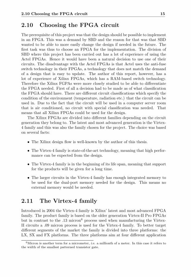
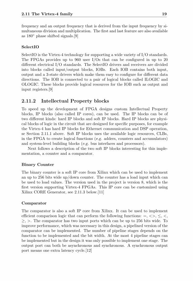
The main logic resource in the Virtex-4 FPGA is the Configurable Logic Blocks(CLBs). The CLBs can be connected to each other via programmable intercon-nections and switching matrices, see Figure 2.8. Each CLB is made up of fourslices. There are two different kinds of slices in each CLB. The two kinds arecalled SLICEM and SLICEL. Common to both of the slices are:
• two function generators (or look-up tables)
• two storage elements
• arithmetic logic gates
• large multiplexers
2.11 The Virtex-4 family 17
• fast carry look-ahead chain
Figure 2.8. The figure shows the arrangement of the slices within the CLB. [9]
SLICEM also has the ability to support two additional functions: storing datausing distributed RAM and shifting data with 16-bit registers.[9]
BlockRAM
Apart from the Distributed RAM situated in the CLBs the Virtex-4 FPGA also haswhat Xilinx calls BlockRAM (short BRAM). These are integrated blocks of mem-ory placed in columns over the entire Virtex-4 chips. Each BlockRAM primitive is16 Kbit (18 Kbit if parity bits are included) and is a true dual-port memory7. Thecircuits comes with varying amounts of BlockRAM, from 864 Kbits in the smallestone up to 9,936 Kbits in the largest FPGA. The primitives can be combined to-gether to form larger memory areas and can be configured to have different widthsand depths. The best and easiest way to combine them is to use Xilinx COREGenerator which is used for customizing hardware resources in the FPGAs, seeSection 2.11.3.[9]
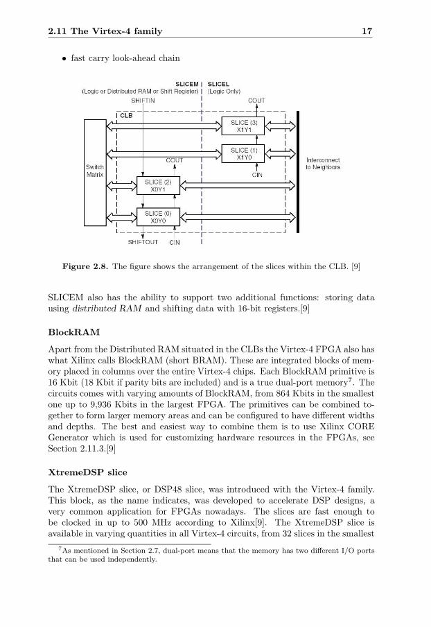
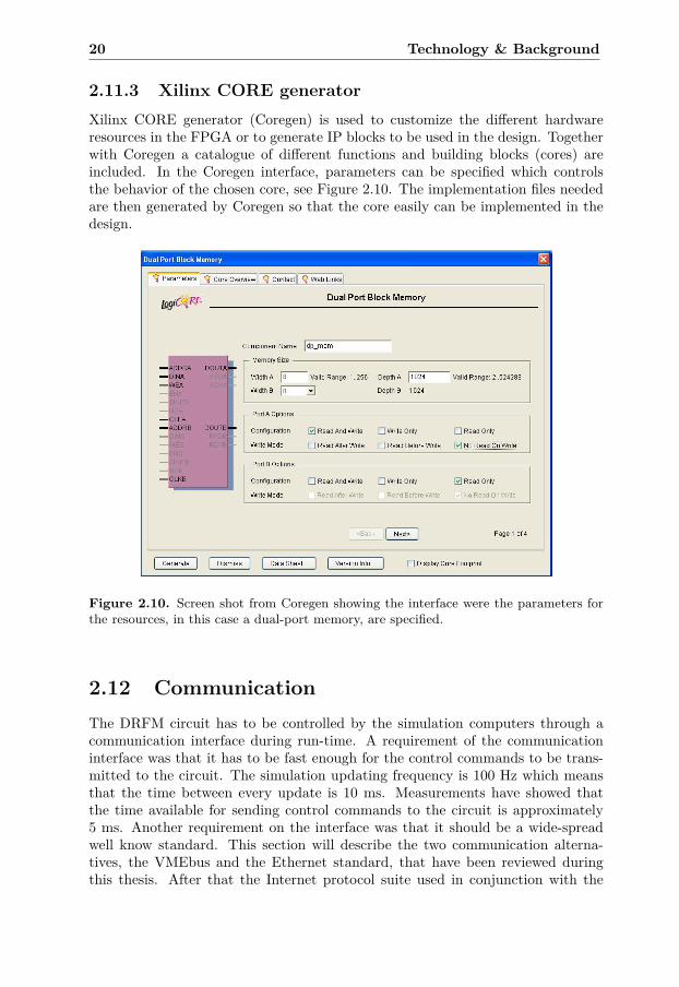
XtremeDSP slice
The XtremeDSP slice, or DSP48 slice, was introduced with the Virtex-4 family.This block, as the name indicates, was developed to accelerate DSP designs, avery common application for FPGAs nowadays. The slices are fast enough tobe clocked in up to 500 MHz according to Xilinx[9]. The XtremeDSP slice isavailable in varying quantities in all Virtex-4 circuits, from 32 slices in the smallest
7As mentioned in Section 2.7, dual-port means that the memory has two different I/O portsthat can be used independently.
18 Technology & Background
circuits to 512 in the largest FPGA. In short the DSP block can be described asan 18x18 multiplier followed by a 3-input adder with a 48-bit output. The blockcan be configured to do various common DSP tasks such as add, multiply, MACC(multiply and accumulate) etc, see Figure 2.9.
Figure 2.9. The figure shows a simplified view of the XtremeDSP slice. The A andB inputs are 18 bits wide and the C input is 48 bits wide. PCIN is an input from acascaded DSP48 slice. The arrows indicates a wire right shift by 17 bits. [10]
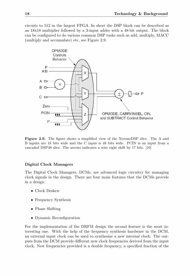
Digital Clock Managers
The Digital Clock Managers, DCMs, are advanced logic circuitry for managingclock signals in the design. There are four main features that the DCMs providein a design:
• Clock Deskew
• Frequency Synthesis
• Phase Shifting
• Dynamic Reconfiguration
For the implementation of the DRFM design the second feature is the most in-teresting one. With the help of the frequency synthesis hardware in the DCM,an external input clock can be used to synthesize a new internal clock. The out-puts from the DCM provide different new clock frequencies derived from the inputclock. New frequencies provided is a double frequency, a specified fraction of the
2.11 The Virtex-4 family 19
frequency and an output frequency that is derived from the input frequency by si-multaneous division and multiplication. The first and last feature are also availableas 180◦ phase shifted signals.[9]
SelectIO
SelectIO is the Virtex-4 technology for supporting a wide variety of I/O standards.The FPGAs provides up to 960 user I/Os that can be configured in up to 20different electrical I/O standards. The SelectIO drivers and receivers are dividedinto blocks called input/output blocks, IOBs. Each IOB contains both input,output and a 3-state drivers which make them easy to configure for different datadirections. The IOB is connected to a pair of logical blocks called ILOGIC andOLOGIC. These blocks provide logical resources for the IOB such as output andinput registers.[9]
2.11.2 Intellectual Property blocksTo speed up the development of FPGA designs custom Intellectual Propertyblocks, IP blocks (also called IP cores), can be used. The IP blocks can be oftwo different kinds: hard IP blocks and soft IP blocks. Hard IP blocks are physi-cal blocks of logic in the circuit that are designed for specific purposes, for examplethe Virtex-4 has hard IP blocks for Ethernet communication and DSP operation,se Section 2.11.1 above. Soft IP blocks uses the available logic resources, CLBs,in the FPGA to create logical functions (e.g. adders, counters and accumulators)and system-level building blocks (e.g. bus interfaces and processors).
Next follows a description of the two soft IP blocks interesting for this imple-mentation, a counter and a comparator.
Binary Counter
The binary counter is a soft IP core from Xilinx which can be used to implementan up to 256 bits wide up/down counter. The counter has a load input which canbe used to load values. The version used in the project is version 8, which is thefirst version supporting Virtex-4 FPGAs. This IP core can be customized usingXilinx CORE Generator, see 2.11.3 below.[11]
Comparator
The comparator is also a soft IP core from Xilinx. It can be used to implementefficient comparison logic that can perform the following functions: =, <>, ≤, <,≥, >. The comparator has two input ports which can be up to 256 bits wide. Toimprove performance, which was necessary in this design, a pipelined version of thecomparator can be implemented. The number of pipeline stages depends on thefunction to be implemented and the bit width. At the most 4 pipeline stages canbe implemented but in the design it was only possible to implement one stage. Theoutput port can both be asynchronous and synchronous. A synchronous outputport means one extra latency cycle.[12]
20 Technology & Background
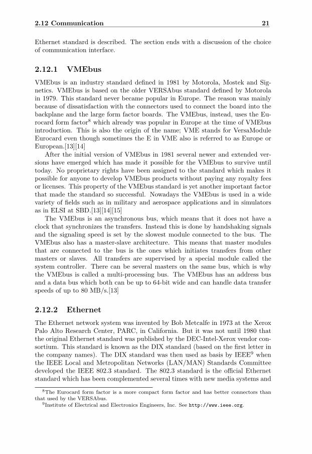
2.11.3 Xilinx CORE generatorXilinx CORE generator (Coregen) is used to customize the different hardwareresources in the FPGA or to generate IP blocks to be used in the design. Togetherwith Coregen a catalogue of different functions and building blocks (cores) areincluded. In the Coregen interface, parameters can be specified which controlsthe behavior of the chosen core, see Figure 2.10. The implementation files neededare then generated by Coregen so that the core easily can be implemented in thedesign.
Figure 2.10. Screen shot from Coregen showing the interface were the parameters forthe resources, in this case a dual-port memory, are specified.
2.12 CommunicationThe DRFM circuit has to be controlled by the simulation computers through acommunication interface during run-time. A requirement of the communicationinterface was that it has to be fast enough for the control commands to be trans-mitted to the circuit. The simulation updating frequency is 100 Hz which meansthat the time between every update is 10 ms. Measurements have showed thatthe time available for sending control commands to the circuit is approximately5 ms. Another requirement on the interface was that it should be a wide-spreadwell know standard. This section will describe the two communication alterna-tives, the VMEbus and the Ethernet standard, that have been reviewed duringthis thesis. After that the Internet protocol suite used in conjunction with the
2.12 Communication 21
Ethernet standard is described. The section ends with a discussion of the choiceof communication interface.
2.12.1 VMEbusVMEbus is an industry standard defined in 1981 by Motorola, Mostek and Sig-netics. VMEbus is based on the older VERSAbus standard defined by Motorolain 1979. This standard never became popular in Europe. The reason was mainlybecause of dissatisfaction with the connectors used to connect the board into thebackplane and the large form factor boards. The VMEbus, instead, uses the Eu-rocard form factor8 which already was popular in Europe at the time of VMEbusintroduction. This is also the origin of the name; VME stands for VersaModuleEurocard even though sometimes the E in VME also is referred to as Europe orEuropean.[13][14]
After the initial version of VMEbus in 1981 several newer and extended ver-sions have emerged which has made it possible for the VMEbus to survive untiltoday. No proprietary rights have been assigned to the standard which makes itpossible for anyone to develop VMEbus products without paying any royalty feesor licenses. This property of the VMEbus standard is yet another important factorthat made the standard so successful. Nowadays the VMEbus is used in a widevariety of fields such as in military and aerospace applications and in simulatorsas in ELSI at SBD.[13][14][15]
The VMEbus is an asynchronous bus, which means that it does not have aclock that synchronizes the transfers. Instead this is done by handshaking signalsand the signaling speed is set by the slowest module connected to the bus. TheVMEbus also has a master-slave architecture. This means that master modulesthat are connected to the bus is the ones which initiates transfers from othermasters or slaves. All transfers are supervised by a special module called thesystem controller. There can be several masters on the same bus, which is whythe VMEbus is called a multi-processing bus. The VMEbus has an address busand a data bus which both can be up to 64-bit wide and can handle data transferspeeds of up to 80 MB/s.[13]
2.12.2 EthernetThe Ethernet network system was invented by Bob Metcalfe in 1973 at the XeroxPalo Alto Research Center, PARC, in California. But it was not until 1980 thatthe original Ethernet standard was published by the DEC-Intel-Xerox vendor con-sortium. This standard is known as the DIX standard (based on the first letter inthe company names). The DIX standard was then used as basis by IEEE9 whenthe IEEE Local and Metropolitan Networks (LAN/MAN) Standards Committeedeveloped the IEEE 802.3 standard. The 802.3 standard is the official Ethernetstandard which has been complemented several times with new media systems and
8The Eurocard form factor is a more compact form factor and has better connectors thanthat used by the VERSAbus.
9Institute of Electrical and Electronics Engineers, Inc. See http://www.ieee.org.
22 Technology & Background
capabilities to form the Ethernet of today. The Ethernet standard contains, forexample, different standards of transfer speeds of which 100 Mbps over twist-paircables (100BASE-TX) is the most used standard in households and companies to-day. This standard is also the standard interesting for this thesis, hence the focuswill be on the 100BASE-TX standard.[16]
To be able to connect to an Ethernet network, an Ethernet interface is needed.The interface is a physical hardware that has all the circuits needed to communi-cate over the network. It can both be free-standing hardware or parts of it couldbe integrated in another circuit, as the integrated Virtex-4 Ethernet MAC.
Every Ethernet interface has a unique 48-bit address which is hard coded tothe physical interface. The 48-bit address is divided into two 24-bit parts. Thefirst half is called the OUI, which stands for Organizationally Unique Identifier.The OUI is a unique 24-bit number assigned by IEEE to every Ethernet vendor.The second half of the 48-bit address is assigned by the vendor and has to be aunique number. The two halves combined makes up the unique 48-bit Ethernetaddress which every Ethernet interface is equipped with. [16]
Data sent over an Ethernet based network is transmitted in Ethernet frames.A frame is a standardized set of bits used to carry data over the Ethernet system.In short the Ethernet frame consists of a header, a data field and a frame checksequence for error detection. The header is 14 byte long and contains the sourceaddress, the destination address and type. The addresses sent in the Ethernetframe are the 48-bit Ethernet addresses. The data to be sent is encapsulatedinside the data part of the frame which can be from 46 bytes up to 1500 bytes.The data part must be at least 46 bytes; otherwise padding data is used to make thedata field 46 bytes. For a more detailed description of Ethernet and the Ethernetframe see [16].
When wanting to network enable a device using off-the-shelf Ethernet productsusually three parts are needed: An Ethernet Media Access Controller, a PhysicalLayer Device and a Registered Jack type 45.
Media Access Controller. The sending and receiving of frames is controlledby the Media Access Control (MAC) protocol (therefore the Ethernet ad-dress, mentioned above, is also called a MAC address). The protocol usedby the MAC is called Carrier Sense Multiple Access Collision Detection(CSMA/CD). Carrier sense means that the protocol listens for activity andsends only if there is no activity on the channel used. Multiple access meansthat multiple nodes can share the same channel. If two nodes are trying touse the channel at the same time it is detected by the collision detection. Themode when using the CSMA/CD protocol is also called half-duplex mode.If two nodes are connected to each other via a dedicated channel full-duplexmode could be used. Dedicated channels are used between, for example, anode and switch. In this case the CSMA/CD protocol is not needed. Thebenefit of full-duplex mode is that both nodes can send at the same timedoubling the transfer speed.[16]
Physical Layer Device. The physical layer device, PHY, is the part of the Eth-ernet interface that handles the physical signaling on the physical medium
2.12 Communication 23
used, e.g. twisted-pair or fiber cable. The PHY is often called a transceiver.The name comes from that it transmits and receives signals. The EMACand the PHY are often connected to each other via a Media IndependentInterface (MII). The MII is a standardized interface between the transceiverand the EMAC used by the 100BASE-TX standard. This makes it possibleto connect different media systems to the Ethernet interface.[16]
Registered Jack type 45. The RJ-45 jack is the connector for the twisted-paircable mentioned earlier. It is connected to the PHY and can be referred toas the Media Dependent Interface (MDI) in opposite to the MII.
2.12.3 The Internet protocol suiteWhen using higher level protocols these are carried inside the data field of theEthernet frame. The protocols interesting for this thesis are the protocols whichare parts of the Internet protocol suite. The suite is also often referred to asthe TCP/IP protocol suite after the two most important protocols: the InternetProtocol (IP) and the Transmission Control Protocol (TCP).
The job of the IP protocol is to move packets of data from a source to adestination. To be able to do that, every interface on an IP network, such as theInternet, is identified by a 32-bit binary number called an IP address. IP carriesdata for several different higher level protocols which are parts of the Internetprotocol suite. If reliable transport over the network is needed, the TCP protocolhas to be used. Several different functions is included in the TCP protocol tosupervise the transport of data packets. For that reason TCP is able to discoverlost packets and resend them if needed. Another protocol often used is the UserDatagram Protocol (UDP). UDP sends and receives datagrams10 but, unlike TCP,UDP has no control of reliability11. UDP is most often used for sending streamingmedia, such as audio and video, were on-time arrival is more important thanreliability.
Even though there are a lot more protocols in the Internet protocol suite, theones previous mentioned are the most interesting one for the DRFM application.Therefore no deeper description of the others will be conducted in this report andthe reader is referred to [17] if more information about the protocol suite is wanted.
2.12.4 Choosing communication interfaceThe most important reason to use the VMEbus for communication was that it isan industry standard and that it already is well-known at SBD. Other importantadvantages of using the VME interface was the speed, the simplicity and thefact that a VMEbus VHDL IP core already had been developed at SBD. Thedisadvantage of VMEbus was the high cost of new hardware if the system wouldhave to be increased in size. Furthermore, more DRFM circuit boards in the newsystem means that the length of the bus had to be increased using so called bus
10Units of information.11I.e. if the datagram reaches its destination or not
24 Technology & Background
repeaters. Not only does this mean a considerably high cost, it also means thatthe speed goes down significantly. Therefore a new cheaper, high speed and well-spread communication standard was of interest. The choice fell on the Ethernetinterface. Ethernet is a very wide spread industry standard for high speed datacommunication. The communication protocol to be used in the simulator can bechosen from a variety of protocols, for example, raw Ethernet, UDP or TCP couldbe used, see Section 2.12.2. The actual choice of protocol is not made during thisthesis, instead it is up to the staff at ELSI to decide, depending on resources andthe speed required.
2.13 Choosing Ethernet interfaceAs the needed Ethernet and Internet protocol technology and acronyms have beendiscussed we are ready to go into the choice of Ethernet interface.
The first alternative to look into was the new Virtex-4 FX family which comeswith integrated Ethernet MAC (EMAC) and PowerPC processor cores. The ideawas to use the EMAC for communication and to use the PowerPC for handlingthe TCP/IP stack. A TCP/IP stack for the PowerPC integrated in the Virtex-4is available from a company called Treck Inc.12. The TCP/IP stack from Treckis designed in cooperation with Xilinx and can be used in the Virtex-4 with thePowerPC processor. When tested on a Virtex-II Pro system a through-put of 785Mb/s [18] has been achieved which is well enough for the requirements of thisproject. The disadvantage of this solution is that much more development timewould have been needed, time which was assumed not available.
Because of the limitations of the project, that is, only the DRFM function wasto be implemented in the FPGA during the given time, a free-standing Ethernetmodule had to be used. Hence, the second alternative was to scan the marketfor ready-to-use Ethernet modules. The market scan resulted in a review of themodules found. The review will serve as a future basis for deciding the Ethernetmodule needed. Before the review, requirements was set up that the module hadto fulfill. Five requirements were identified:
• High enough data transfer speed
• Available TCP/IP stack
• Small enough to fit on a circuit board
• Preferably both TP port, PHY and MAC available on the module
• Availability on the market
These requirements are used in Section 2.13 to make a preliminary choice ofEthernet module. But first, the module reviews:
12Treck Inc. is a company that has been designing real-time embedded internet protocols since1997, see http://www.treck.com/
2.13 Choosing Ethernet interface 25
Rabbit RCM3200
Rabbit Semiconductors 13 is a fabless semiconductor company that is specialized inhigh-performance 8-bit microprocessors. They have also developed several differentEthernet modules that uses their microprocessors. The most interesting module,which best suits this projects requirements, is the Rabbit RCM3200 module. Thisis a small Ethernet module which consists of a Rabbit 3000 microprocessor, anEthernet controller, memory and a 10/100 Ethernet port. The Rabbit 3000 isan 8-bit microprocessor and runs at up to 44.2 MHz. It can be programmedusing a development system called Dynamic C. Together with the developmentsystem comes a royalty-free TCP/IP stack (and the source code). According tothe RCM3200 FAQ [19] the current maximum receive speed is approximately 3Mbps using TCP/IP on the RCM3200.[20]
Netburner Mod5282
Netburner14 is a company that provides embedded Ethernet for quick network en-abling of products. The Netburner Mod5282 is a small Ethernet module based onthe Coldfire MCF5282 processor from Freescale Semiconductor (former Motorola).The MCF5282 is a 32-bit processor, runs at up to 66 MHz and has a built in 10/100Ethernet MAC. No throughput information is available for the Mod5282 module.A good guess is that the throughput will be better then the RCM3200 module be-cause of the more powerful processor handling the communication protocols.[21]
Epson S1S60000
The Epson15 S1S60000 is a network controller with built-in TCP/IP protocol(firmware). It is a single chip, thus it has to be complemented with a PHY chipand a RJ-45 port. The controller can be controlled through GPIO’s. Accordingto the manual for the circuit the maximum effective transfer rate (over UDP) isapproximately 5.5 Mbps for the S1S60000 circuit [22]. Worth to notice is thata new chip called S1S60020 based on the S1S60000 is under development. Thepreliminary data sheet for the chip claims that a throughput of 20 Mbps or morecould be achieved [23]. The primary reason for the boost in throughput over theolder chip is the hard-wiring of some portions of the processing.
WizNet NM7010B
WizNet16 is a Korean company that has developed completely hard wired TCP/IPand Ethernet MAC chip. The most recent is called W3150. WIZnet has combinedthis chip together with a 10/100 Ethernet PHY and an Ethernet port to theNM7010B module. The data sheet for the NM7010B was not available at theWIZnet home page during the writing of this review. Hence no speed informa-tion for the module is available. Information on the home page for the W3150
13http://www.rabbitsemiconductor.com14http://www.netburner.com15http://www.epson-electronics.de16http://www.wiznet.co.kr
26 Technology & Background
chip, on the other hand, claims that the throughput of the chip can be up to 11Mbps depending heavily on the CPU controlling the chip. The real throughput issomewhat unclear due to the fact that the maximum throughput according to theW3150 Brochure is claimed to be up to 25 Mbps [24].
2.13.1 The choice of Ethernet moduleThe first thing to be said is that no real component selection will be done duringthis thesis. The final selection will not be done until the DRFM circuit board willbe designed. This review and choice of Ethernet module is more of a proposal andserves as basic data for decision-making.
Three important properties of the wanted modules have been identified. Thethree properties are
• data transfer speed
• the easiness of implementing the interface
• the documentation of the interface
Starting with the speed issue a simple estimation of the needed data transferspeed is approximately 4.5 Mbps, see Example 2.2. Except the Netburner module(which has no speed data) and the Rabbit module (having only 3 Mbps receivingspeed) the two other modules could live up to the requirement. As always withperformance measures of computer products values of speed can not be taken tooserious. E.g. it is hard to tell under what conditions the throughput values havebeen measured and what protocols have been used.
The WIZNet, Netburner and Rabbit modules are all complete with PHY chipand RJ-45 port whereas the Epson chip has to be completed with the PHY chipand port. This makes the first three modules easier to handle and to connect tothe DRFM circuit board. All modules except WIZNets has good or very gooddocumentation. The problem with WIZNets documentation is the lack of correct(and understandable) English and the slow and hard navigated home page.
Summing up the properties wanted neither of the modules could live up toall of the requirements. A decision had to be made anyway and the choice fellon the Netburner module. This module has good documentation and is easy toimplement in a design. It lacks specification of data transfer speed but as the pro-cessor equipped on the module is rather powerful a good guess is that the speedrequirement will be easy to live up to. Another advantage is that the CPU on themodule could be used for other calculations and not only for the communication.Hence a development kit for the Mod5282 and an extra Mod5282 has been boughtby SBD and speed measurements will be done after this thesis has come to an end.
Example 2.2: Calculation of data transfer speedThis example is intended to give an approximate calculation of the transfer speedneeded to update the DRFM circuit with control data during run-time.
2.13 Choosing Ethernet interface 27
An overestimation is that forty 24 bit commands have to be sent to the Ethernetmodule every cycle during run-time. This makes a total of
40× 24 bit = 960 bit
to be sent to every DRFM circuit connected to the Ethernet module. At the mostfour DRFM circuits will be connected to the same Ethernet module which makesa total of
960× 4 bit = 3840 bit
that has to be sent every simulation cycle. To be able to calculate the correct datatransfer speed the header of the used communication protocols also needs to betaken into account. Different protocols could be used for communication, the finaldecision of protocol is not made during the work of this thesis, but a good guessis that the UDP or the TCP protocol will be used. Of these two protocols, TCPhas the largest header. The TCP header can be up to 60 bytes. The TCP frameis encapsulated inside an IP frame which header also can be up to 60 bytes. Thismakes a total of
38408
bytes + 2× 60 bytes = 600 bytes
The IP frame in its turn is encapsulated inside the data part of an Ethernet frame.The Ethernet header is always 14 bytes. Therefore totally
600 bytes + 14 bytes = 614 bytes
have to be sent every simulation cycle. The simulator is updated at 100 Hz whichmakes every cycle 10 ms. Unfortunately the whole cycle cannot be used to senddata though. A part of it will be used for other processes on the CPU controllingthe DRFM circuits. A low estimation is that 1 ms can be used for sending controldata17. This finally makes the data transfer speed needed
6141× 10−3
MB/s = 614 kB/s ≈ 4.9 Mbps
[17]
17Measurements of the processes have showed that half of the cycle, 5 ms, is available forsending control data to the DRFM circuits. In this case, 1 ms is used to approximate the resultin the right direction.

28 Technology & Background
Chapter 3
Implementation & Testing
This chapter starts with a description of the layout decisions made and the imple-mentation flow used. A short discussion is held around the tools used for the im-plementation of the design. After that the resulting layout of the design is describedin detail. The chapter ends with a discussion of the method used for validating thedesign.
3.1 Layout decisionsSeveral layout decisions of the DRFM design had to be made. The first was tostudy the old design to figure out the purpose of the different logical blocks used.This was done to better understand how the new circuit should work and to beable to reuse some of the design ideas in the new implementation. Even thoughno code was reused this made the development of the design faster.
After having studied the old design and the requirements of the new design,three major building blocks were identified:
1. A dual-port memory to be used for storing the wave forms.
2. An interface used for communication with the simulator computer.
3. A control logic block which controls the behavior of the DRFM circuit duringrun-time.
3.1.1 The memoryA decision that had to be made was how to implement the memory needed tostore the wave forms. One alternative was to use an external memory. This wouldhave meant that a memory interface had to be implemented in the FPGA. Thedisadvantage with and external memory is that an extra physical component hadto be connected to the circuit board. A more interesting alternative was instead toimplement the memory using the integrated memory blocks in the Virtex-4 circuit.Using these blocks no external component was required and the design would also
29
30 Implementation & Testing
be easier to alter. Consequently BlockRAM was decided to be used in the DRFMas the memory resource.
3.1.2 The interfaceAn interface communicating with the simulation computer was also needed. Fromthe beginning the requisite from SBD was that the interface should be a VMEbusinterface. As discussed in Section 2.12, the reason for that was that the VMEbuswas well known by the ELSI staff, for example, the simulation computers usesVMEbus. A VHDL implementation of the VMEbus was also already available atSBD making it a lot faster to implement. The drawback of using the VMEbuswas the cost of the VME equipment needed for the new DRFM circuit boards.Another important disadvantage is the fact that if more slots for the new circuitboards will be needed, a bus repeater has to be used, which makes the speed ofthe VMEbus drop significantly. Another high speed, cheap, industry standard wasrequired.
The choice fell on the Ethernet standard and more precisely the 100BASE-TX standard1. The Ethernet standard is a widely used local area networkingtechnology. The standard is rather complex to implement in an FPGA but insteadof implementing it, an external Ethernet module could be purchased to quicklyEthernet-enable a product. There are several different Ethernet chips and modulesavailable on the market. In this case these could be used to apply an Ethernetinterface to the DRFM circuit.
3.2 The design flowThe design was implemented using VHDL code. VHDL is an acronym for VHSICHardware Description Language. VHSIC, in its turn, is an acronym for Very HighSpeed Integrated Circuit. The use of VHDL was a demand by SBD due to the factthat VHDL is the most commonly used hardware description language at SBD.A hardware description language is used to describe the logic to be implementedin an FPGA. The design phase starts with describing the most primitive parts ofthe system such as counters and registers. These are combined and connected toeach other to form larger, more complex, building blocks of logic. At the end allthe logic blocks are combined to form the final design.
When designing logic to be implemented in an FPGA a certain design flow isfollowed. This flow goes through the different phases of the implementation andmust be followed to be able to complete the design. Normally the design flow is nota straight road to the end goal: the final design. Instead the functional behaviorof the design is verified at different stages in the flow. Should the function failfor some reason an attempt to correct the mistake has to be made in the VHDLcode. Thus, the designer often goes through several iterations of the design flowbefore the final circuit is ready. In Figure 3.1 on page 31 the design flow followedduring the implementation of the DRFM circuit is visualized. The arrows going
1100 Mbit over twisted-pair cables
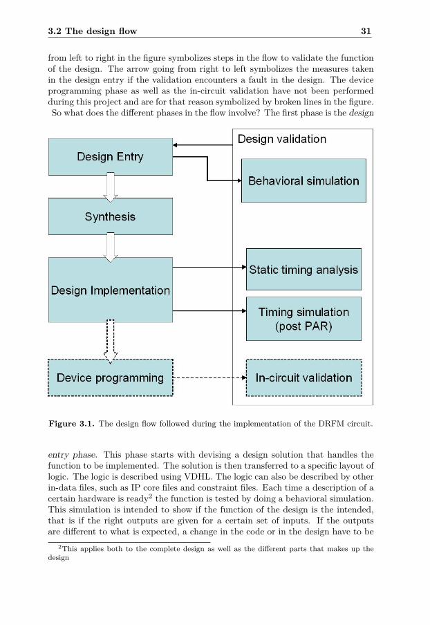
3.2 The design flow 31
from left to right in the figure symbolizes steps in the flow to validate the functionof the design. The arrow going from right to left symbolizes the measures takenin the design entry if the validation encounters a fault in the design. The deviceprogramming phase as well as the in-circuit validation have not been performedduring this project and are for that reason symbolized by broken lines in the figure.So what does the different phases in the flow involve? The first phase is the design
Figure 3.1. The design flow followed during the implementation of the DRFM circuit.
entry phase. This phase starts with devising a design solution that handles thefunction to be implemented. The solution is then transferred to a specific layout oflogic. The logic is described using VDHL. The logic can also be described by otherin-data files, such as IP core files and constraint files. Each time a description of acertain hardware is ready2 the function is tested by doing a behavioral simulation.This simulation is intended to show if the function of the design is the intended,that is if the right outputs are given for a certain set of inputs. If the outputsare different to what is expected, a change in the code or in the design have to be
2This applies both to the complete design as well as the different parts that makes up thedesign
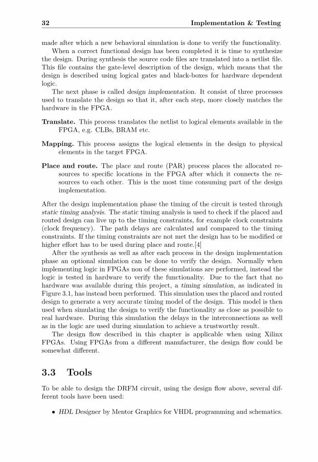
32 Implementation & Testing
made after which a new behavioral simulation is done to verify the functionality.When a correct functional design has been completed it is time to synthesize
the design. During synthesis the source code files are translated into a netlist file.This file contains the gate-level description of the design, which means that thedesign is described using logical gates and black-boxes for hardware dependentlogic.
The next phase is called design implementation. It consist of three processesused to translate the design so that it, after each step, more closely matches thehardware in the FPGA.
Translate. This process translates the netlist to logical elements available in theFPGA, e.g. CLBs, BRAM etc.
Mapping. This process assigns the logical elements in the design to physicalelements in the target FPGA.
Place and route. The place and route (PAR) process places the allocated re-sources to specific locations in the FPGA after which it connects the re-sources to each other. This is the most time consuming part of the designimplementation.
After the design implementation phase the timing of the circuit is tested throughstatic timing analysis. The static timing analysis is used to check if the placed androuted design can live up to the timing constraints, for example clock constraints(clock frequency). The path delays are calculated and compared to the timingconstraints. If the timing constraints are not met the design has to be modified orhigher effort has to be used during place and route.[4]
After the synthesis as well as after each process in the design implementationphase an optional simulation can be done to verify the design. Normally whenimplementing logic in FPGAs non of these simulations are performed, instead thelogic is tested in hardware to verify the functionality. Due to the fact that nohardware was available during this project, a timing simulation, as indicated inFigure 3.1, has instead been performed. This simulation uses the placed and routeddesign to generate a very accurate timing model of the design. This model is thenused when simulating the design to verify the functionality as close as possible toreal hardware. During this simulation the delays in the interconnections as wellas in the logic are used during simulation to achieve a trustworthy result.
The design flow described in this chapter is applicable when using XilinxFPGAs. Using FPGAs from a different manufacturer, the design flow could besomewhat different.
3.3 ToolsTo be able to design the DRFM circuit, using the design flow above, several dif-ferent tools have been used:
• HDL Designer by Mentor Graphics for VHDL programming and schematics.
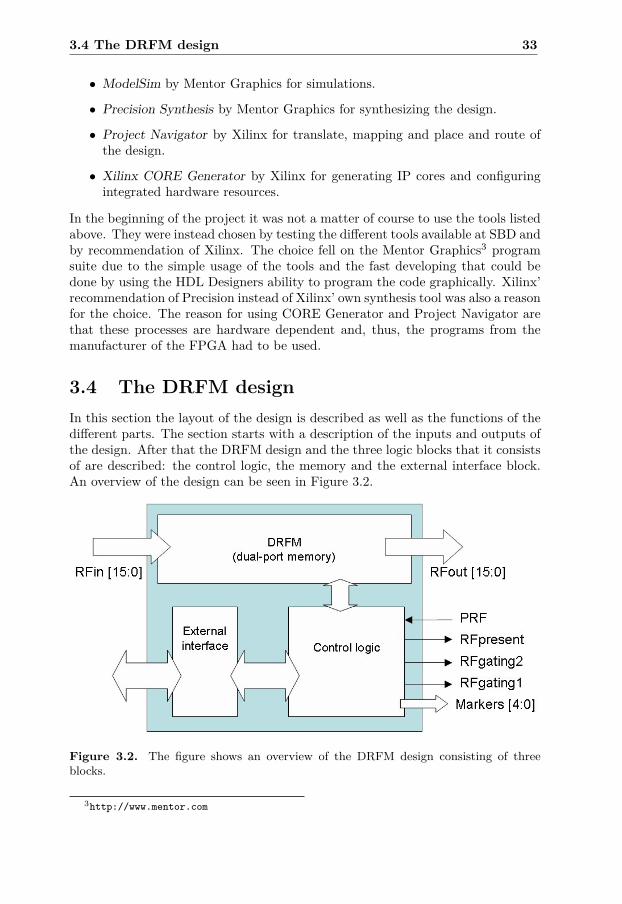
3.4 The DRFM design 33
• ModelSim by Mentor Graphics for simulations.
• Precision Synthesis by Mentor Graphics for synthesizing the design.
• Project Navigator by Xilinx for translate, mapping and place and route ofthe design.
• Xilinx CORE Generator by Xilinx for generating IP cores and configuringintegrated hardware resources.
In the beginning of the project it was not a matter of course to use the tools listedabove. They were instead chosen by testing the different tools available at SBD andby recommendation of Xilinx. The choice fell on the Mentor Graphics3 programsuite due to the simple usage of the tools and the fast developing that could bedone by using the HDL Designers ability to program the code graphically. Xilinx’recommendation of Precision instead of Xilinx’ own synthesis tool was also a reasonfor the choice. The reason for using CORE Generator and Project Navigator arethat these processes are hardware dependent and, thus, the programs from themanufacturer of the FPGA had to be used.
3.4 The DRFM designIn this section the layout of the design is described as well as the functions of thedifferent parts. The section starts with a description of the inputs and outputs ofthe design. After that the DRFM design and the three logic blocks that it consistsof are described: the control logic, the memory and the external interface block.An overview of the design can be seen in Figure 3.2.
Figure 3.2. The figure shows an overview of the DRFM design consisting of threeblocks.
3http://www.mentor.com
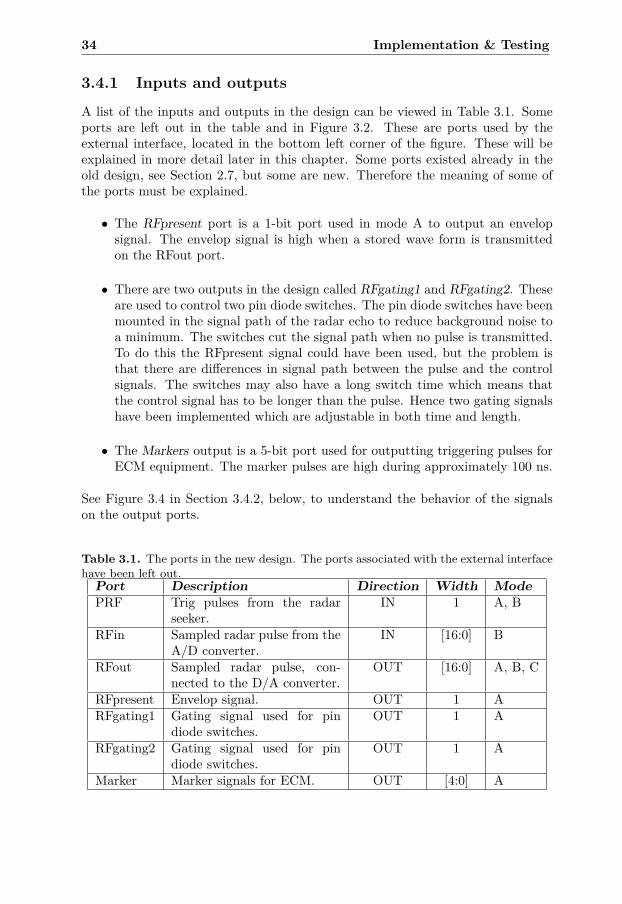
34 Implementation & Testing
3.4.1 Inputs and outputs
A list of the inputs and outputs in the design can be viewed in Table 3.1. Someports are left out in the table and in Figure 3.2. These are ports used by theexternal interface, located in the bottom left corner of the figure. These will beexplained in more detail later in this chapter. Some ports existed already in theold design, see Section 2.7, but some are new. Therefore the meaning of some ofthe ports must be explained.
• The RFpresent port is a 1-bit port used in mode A to output an envelopsignal. The envelop signal is high when a stored wave form is transmittedon the RFout port.
• There are two outputs in the design called RFgating1 and RFgating2. Theseare used to control two pin diode switches. The pin diode switches have beenmounted in the signal path of the radar echo to reduce background noise toa minimum. The switches cut the signal path when no pulse is transmitted.To do this the RFpresent signal could have been used, but the problem isthat there are differences in signal path between the pulse and the controlsignals. The switches may also have a long switch time which means thatthe control signal has to be longer than the pulse. Hence two gating signalshave been implemented which are adjustable in both time and length.
• The Markers output is a 5-bit port used for outputting triggering pulses forECM equipment. The marker pulses are high during approximately 100 ns.
See Figure 3.4 in Section 3.4.2, below, to understand the behavior of the signalson the output ports.
Table 3.1. The ports in the new design. The ports associated with the external interfacehave been left out.
Port Description Direction Width ModePRF Trig pulses from the radar
seeker.IN 1 A, B
RFin Sampled radar pulse from theA/D converter.
IN [16:0] B
RFout Sampled radar pulse, con-nected to the D/A converter.
OUT [16:0] A, B, C
RFpresent Envelop signal. OUT 1 ARFgating1 Gating signal used for pin
diode switches.OUT 1 A
RFgating2 Gating signal used for pindiode switches.
OUT 1 A
Marker Marker signals for ECM. OUT [4:0] A
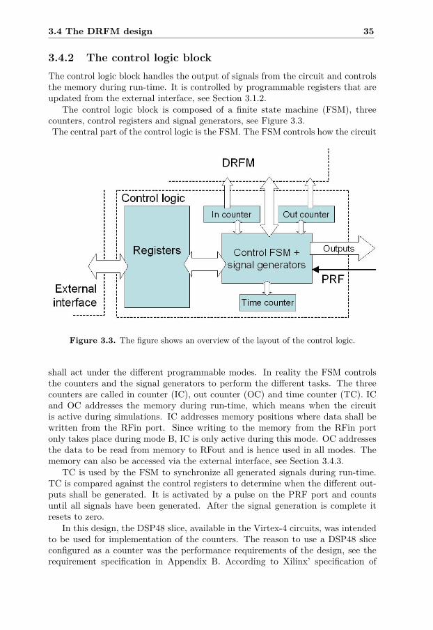
3.4 The DRFM design 35
3.4.2 The control logic blockThe control logic block handles the output of signals from the circuit and controlsthe memory during run-time. It is controlled by programmable registers that areupdated from the external interface, see Section 3.1.2.
The control logic block is composed of a finite state machine (FSM), threecounters, control registers and signal generators, see Figure 3.3.The central part of the control logic is the FSM. The FSM controls how the circuit
Figure 3.3. The figure shows an overview of the layout of the control logic.
shall act under the different programmable modes. In reality the FSM controlsthe counters and the signal generators to perform the different tasks. The threecounters are called in counter (IC), out counter (OC) and time counter (TC). ICand OC addresses the memory during run-time, which means when the circuitis active during simulations. IC addresses memory positions where data shall bewritten from the RFin port. Since writing to the memory from the RFin portonly takes place during mode B, IC is only active during this mode. OC addressesthe data to be read from memory to RFout and is hence used in all modes. Thememory can also be accessed via the external interface, see Section 3.4.3.
TC is used by the FSM to synchronize all generated signals during run-time.TC is compared against the control registers to determine when the different out-puts shall be generated. It is activated by a pulse on the PRF port and countsuntil all signals have been generated. After the signal generation is complete itresets to zero.
In this design, the DSP48 slice, available in the Virtex-4 circuits, was intendedto be used for implementation of the counters. The reason to use a DSP48 sliceconfigured as a counter was the performance requirements of the design, see therequirement specification in Appendix B. According to Xilinx’ specification of
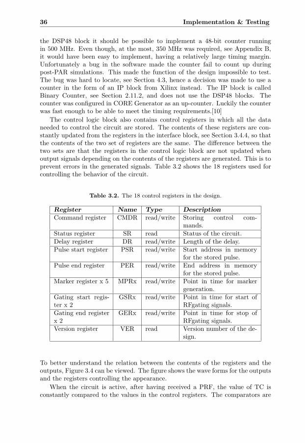
36 Implementation & Testing
the DSP48 block it should be possible to implement a 48-bit counter runningin 500 MHz. Even though, at the most, 350 MHz was required, see Appendix B,it would have been easy to implement, having a relatively large timing margin.Unfortunately a bug in the software made the counter fail to count up duringpost-PAR simulations. This made the function of the design impossible to test.The bug was hard to locate, see Section 4.3, hence a decision was made to use acounter in the form of an IP block from Xilinx instead. The IP block is calledBinary Counter, see Section 2.11.2, and does not use the DSP48 blocks. Thecounter was configured in CORE Generator as an up-counter. Luckily the counterwas fast enough to be able to meet the timing requirements.[10]
The control logic block also contains control registers in which all the dataneeded to control the circuit are stored. The contents of these registers are con-stantly updated from the registers in the interface block, see Section 3.4.4, so thatthe contents of the two set of registers are the same. The difference between thetwo sets are that the registers in the control logic block are not updated whenoutput signals depending on the contents of the registers are generated. This is toprevent errors in the generated signals. Table 3.2 shows the 18 registers used forcontrolling the behavior of the circuit.
Table 3.2. The 18 control registers in the design.
Register Name Type DescriptionCommand register CMDR read/write Storing control com-
mands.Status register SR read Status of the circuit.Delay register DR read/write Length of the delay.Pulse start register PSR read/write Start address in memory
for the stored pulse.Pulse end register PER read/write End address in memory
for the stored pulse.Marker register x 5 MPRx read/write Point in time for marker
generation.Gating start regis-ter x 2
GSRx read/write Point in time for start ofRFgating signals.
Gating end registerx 2
GERx read/write Point in time for stop ofRFgating signals.
Version register VER read Version number of the de-sign.
To better understand the relation between the contents of the registers and theoutputs, Figure 3.4 can be viewed. The figure shows the wave forms for the outputsand the registers controlling the appearance.
When the circuit is active, after having received a PRF, the value of TC isconstantly compared to the values in the control registers. The comparators are
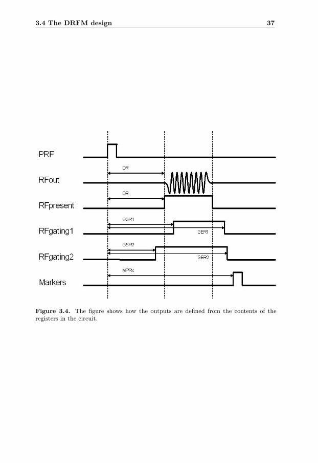
3.4 The DRFM design 37
Figure 3.4. The figure shows how the outputs are defined from the contents of theregisters in the circuit.
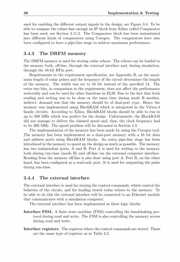
38 Implementation & Testing
used for enabling the different output signals in the design, see Figure 3.4. To beable to compare the values fast enough an IP block from Xilinx called Comparatorhas been used, see Section 2.11.2. The Comparator block has been instantiatedinto different kinds of comparators using Coregen. The comparators have alsobeen configured to have a pipe-line stage to achieve maximum performance.
3.4.3 The DRFM memoryThe DRFM memory is used for storing radar echoes. The echoes can be loaded tothe memory both, off-line, through the external interface and, during simulation,through the 16-bit RFin port.
Requirements in the requirement specification, see Appendix B, on the maxi-mum length of radar pulses and the frequency of the circuit determines the lengthof the memory. The width was set to 16 bit instead of the specified 14. Theextra two bits, in comparison to the requirement, does not affect the performancenoticeably and can be used for other functions in ELSI. Due to the fact that bothreading and writing was to be done at the same time during mode B another,indirect, demand was that the memory should be of dual-port type. Hence thememory was implemented using BlockRAM which is integrated in the Virtex-4family circuits. According to Xilinx, BlockRAM blocks should be able to run inup to 500 MHz which was perfect for the design. Unfortunately, the BlockRAMdid not manage to deliver the claimed speed and, thus, the clock frequency hadto be 200 MHz. The speed problem will be discussed in Section 4.3.
The implementation of the memory has been made by using the Coregen tool.The memory has been implemented as a dual-port memory with a 16 bit dataand address ports using BlockRAM blocks. An extra pipe-line stage has beenintroduced in the memory to speed up the design as much as possible. The memoryhas two independent ports, A and B. Port A is used for writing to the memoryboth during run-time (mode B) and off-line via the external computer interface.Reading from the memory off-line is also done using port A. Port B, on the otherhand, has been configured as a read-only port. It is used for outputting the pulseduring run-time.
3.4.4 The external interfaceThe external interface is used for storing the control commands, which control thebehavior of the circuit, and for loading stored radar echoes to the memory. Tobe able to do this the external interface will be connected to an Ethernet modulethat communicates with a simulation computer.
The external interface has been implemented as three logic blocks:
Interface FSM. A finite state machine (FSM) controlling the handshaking pro-tocol during read and write. The FSM is also controlling the memory accessduring read and write.
Interface registers. The registers where the control commands are stored. Theseare the same type of registers as in Table 3.2.
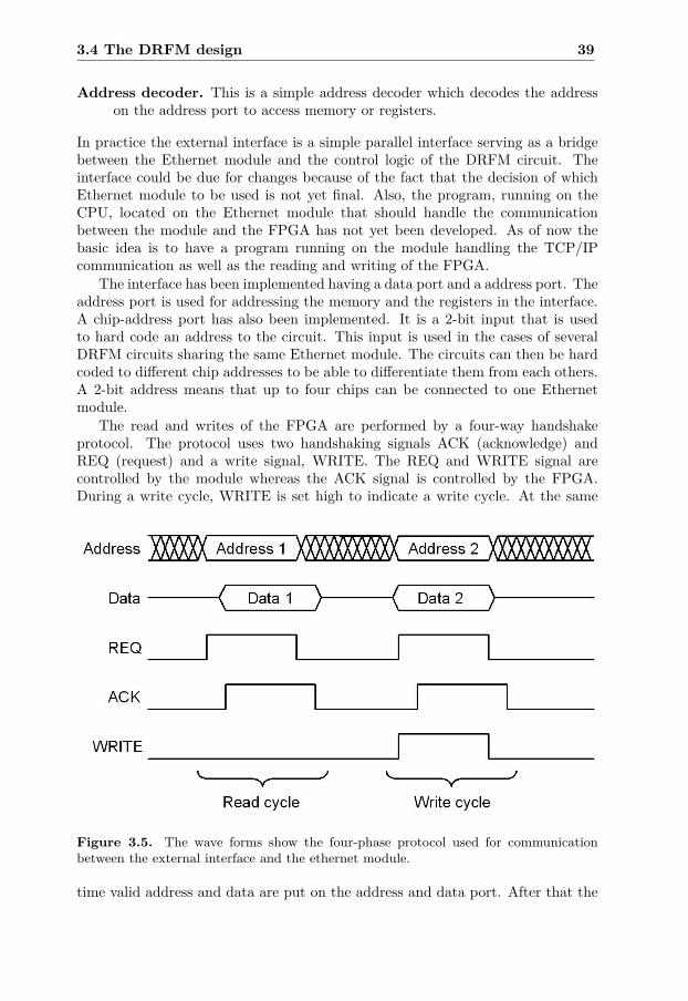
3.4 The DRFM design 39
Address decoder. This is a simple address decoder which decodes the addresson the address port to access memory or registers.
In practice the external interface is a simple parallel interface serving as a bridgebetween the Ethernet module and the control logic of the DRFM circuit. Theinterface could be due for changes because of the fact that the decision of whichEthernet module to be used is not yet final. Also, the program, running on theCPU, located on the Ethernet module that should handle the communicationbetween the module and the FPGA has not yet been developed. As of now thebasic idea is to have a program running on the module handling the TCP/IPcommunication as well as the reading and writing of the FPGA.
The interface has been implemented having a data port and a address port. Theaddress port is used for addressing the memory and the registers in the interface.A chip-address port has also been implemented. It is a 2-bit input that is usedto hard code an address to the circuit. This input is used in the cases of severalDRFM circuits sharing the same Ethernet module. The circuits can then be hardcoded to different chip addresses to be able to differentiate them from each others.A 2-bit address means that up to four chips can be connected to one Ethernetmodule.
The read and writes of the FPGA are performed by a four-way handshakeprotocol. The protocol uses two handshaking signals ACK (acknowledge) andREQ (request) and a write signal, WRITE. The REQ and WRITE signal arecontrolled by the module whereas the ACK signal is controlled by the FPGA.During a write cycle, WRITE is set high to indicate a write cycle. At the same
Figure 3.5. The wave forms show the four-phase protocol used for communicationbetween the external interface and the ethernet module.
time valid address and data are put on the address and data port. After that the
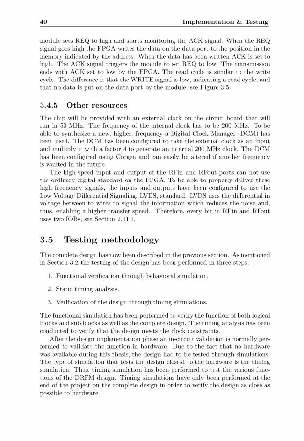
40 Implementation & Testing
module sets REQ to high and starts monitoring the ACK signal. When the REQsignal goes high the FPGA writes the data on the data port to the position in thememory indicated by the address. When the data has been written ACK is set tohigh. The ACK signal triggers the module to set REQ to low. The transmissionends with ACK set to low by the FPGA. The read cycle is similar to the writecycle. The difference is that the WRITE signal is low, indicating a read cycle, andthat no data is put on the data port by the module, see Figure 3.5.
3.4.5 Other resourcesThe chip will be provided with an external clock on the circuit board that willrun in 50 MHz. The frequency of the internal clock has to be 200 MHz. To beable to synthesize a new, higher, frequency a Digital Clock Manager (DCM) hasbeen used. The DCM has been configured to take the external clock as an inputand multiply it with a factor 4 to generate an internal 200 MHz clock. The DCMhas been configured using Corgen and can easily be altered if another frequencyis wanted in the future.
The high-speed input and output of the RFin and RFout ports can not usethe ordinary digital standard on the FPGA. To be able to properly deliver thesehigh frequency signals, the inputs and outputs have been configured to use theLow Voltage Differential Signaling, LVDS, standard. LVDS uses the differential involtage between to wires to signal the information which reduces the noise and,thus, enabling a higher transfer speed.. Therefore, every bit in RFin and RFoutuses two IOBs, see Section 2.11.1.
3.5 Testing methodologyThe complete design has now been described in the previous section. As mentionedin Section 3.2 the testing of the design has been performed in three steps:
1. Functional verification through behavioral simulation.
2. Static timing analysis.
3. Verification of the design through timing simulations.
The functional simulation has been performed to verify the function of both logicalblocks and sub blocks as well as the complete design. The timing analysis has beenconducted to verify that the design meets the clock constraints.
After the design implementation phase an in-circuit validation is normally per-formed to validate the function in hardware. Due to the fact that no hardwarewas available during this thesis, the design had to be tested through simulations.The type of simulation that tests the design closest to the hardware is the timingsimulation. Thus, timing simulation has been performed to test the various func-tions of the DRFM design. Timing simulations have only been performed at theend of the project on the complete design in order to verify the design as close aspossible to hardware.
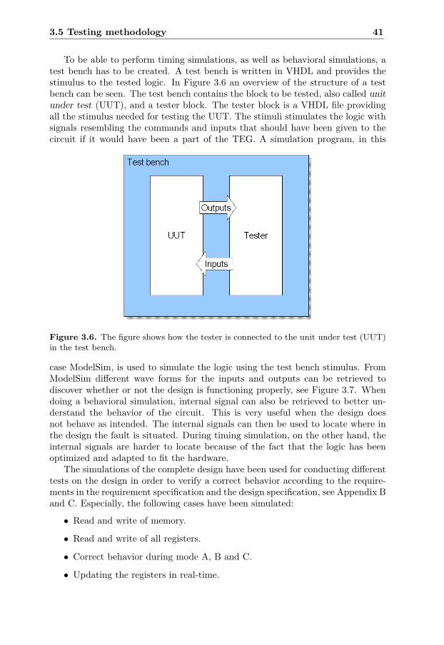
3.5 Testing methodology 41
To be able to perform timing simulations, as well as behavioral simulations, atest bench has to be created. A test bench is written in VHDL and provides thestimulus to the tested logic. In Figure 3.6 an overview of the structure of a testbench can be seen. The test bench contains the block to be tested, also called unitunder test (UUT), and a tester block. The tester block is a VHDL file providingall the stimulus needed for testing the UUT. The stimuli stimulates the logic withsignals resembling the commands and inputs that should have been given to thecircuit if it would have been a part of the TEG. A simulation program, in this
Figure 3.6. The figure shows how the tester is connected to the unit under test (UUT)in the test bench.
case ModelSim, is used to simulate the logic using the test bench stimulus. FromModelSim different wave forms for the inputs and outputs can be retrieved todiscover whether or not the design is functioning properly, see Figure 3.7. Whendoing a behavioral simulation, internal signal can also be retrieved to better un-derstand the behavior of the circuit. This is very useful when the design doesnot behave as intended. The internal signals can then be used to locate where inthe design the fault is situated. During timing simulation, on the other hand, theinternal signals are harder to locate because of the fact that the logic has beenoptimized and adapted to fit the hardware.
The simulations of the complete design have been used for conducting differenttests on the design in order to verify a correct behavior according to the require-ments in the requirement specification and the design specification, see Appendix Band C. Especially, the following cases have been simulated:
• Read and write of memory.
• Read and write of all registers.
• Correct behavior during mode A, B and C.
• Updating the registers in real-time.
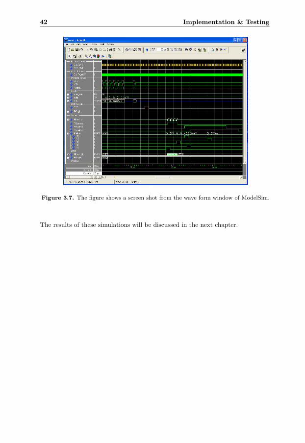
42 Implementation & Testing
Figure 3.7. The figure shows a screen shot from the wave form window of ModelSim.
The results of these simulations will be discussed in the next chapter.
Chapter 4
Results & Discussion
This chapter presents the results of this master’s thesis: a DRFM design that canbe implemented in an FPGA and used in ELSI. Simulations of the functionalityof the design are reviewed. The simulations are presented in forms of wave formsgenerated by ModelSim. The chapter ends with a discussion about the difficultieswhich came up during the project.
4.1 ResultsThis project has resulted in a DRFM design to be used in the ELSI simulator.The design has been tested according to the test methodology in Section 3.5.All relevant requirements in the requirement specification as well as the designspecification have been tested. This has showed that the design lives up to allpriority 1 requirements from the requirement specification, see Appendix B. Thedesign also complies with all but two of the priority 2 requirements. The firstis Req. No. 9, regarding a clock frequency of 350 MHz. This requirement andthe circumstances around it are discussed in Section 4.2. The second is Req.No. 28, regarding an extended design for radar seekers of high PRF type. Thisrequirement was not possible to meet, mainly due to lack of time. This extendeddesign is instead proposed as future work in Section 5.2.
In the next section, timing simulations of the most interesting functions of thedesign are presented.
4.1.1 Cases tested through simulationNext follows a more detailed description of the timing simulations listed in Sec-tion 3.5, as well as references to figures in Appendix D showing the resulting waveforms from ModelSim.
Read and write of memory This test was intended to show that the memorycan be read and written, see Figure D.1. It also shows that when a memory positionis read that has not previously been written to, the output from the memory is
43
44 Results & Discussion
zero. This simulation, as well as the next, also shows the signals associated withthe external computer interface in action.
Read and write of all registers This test has been divided into two figures,see Figure D.2 and D.3. The test is intended to show that all registers can bewritten and read. It also shows that if a read-only register is written the contentof that register does not change. And if an invalid register address is written orread nothing happens1, see Table 4.1 for the register addresses.
Correct behavior during mode A, B and C These simulations shows thebehavior of the circuit when loaded with the values according to Table 4.1 in thethree modes, see Figure D.4, D.5 and D.6. Earlier in the simulations of mode Aand C (not shown in the figures) a wave form has been loaded to the memory.All markers have been set active which corresponds to the marker signals of thefigures of mode A and B. Even though no exact measurements of the delays can beperformed in the wave form figures, the distance between the PRF signal and theoutputs are in accordance with the contents of the corresponding registers. Thestrange appearance of the wave form on RFout is due to glitches on the outputs.This will however not affect external equipments as RFout will be clocked into aDAC before leaving the DRFM circuit board.
Table 4.1. Table over the register settings during the timing simulations of the completedesign.
Register Address ValueCommand register 00 Depending on modeStatus register (read-only) 01 Depending on modeDelay register 02 100Pulse start register 03 52Pulse end register 04 100Marker register 1 05 100Marker register 2 06 200Marker register 3 07 150Marker register 4 08 300Marker register 5 09 190Gating start register 1 10 190Gating end register 1 11 390Gating start register 2 12 220Gating end register 2 13 450Version register (read-only) 14 1
Updating registers in real-time This simulation shows both that the registerscan be updated in real-time as well as updating them will not effect on-goingoutputs (in accordance with Req. No. 23 and 24). During the update two of the
1Reading of such a register address outputs a zero on the data port
4.2 Performance 45
markers are turned off. The delay of the outputs are also changed in comparisonto the values in Table 4.1. The wave forms can be seen in Figure D.7.
4.2 PerformanceThe goal was to meet the priority 2 performance requirement, see Req. No. 8 and9 in Appendix B, of running the circuit in 350 MHz. Unfortunately, even thougha considerably amount of time was put into trying to meet the requirement, thisgoal was impossible to reach. The main reason for not being able to reach it wasthe integrated memory used for the DRFM. The blocks that the memory consistsof are specified for up to 500 MHz each. But when combining several of them theactual performance was much less then that. This is due to that when combiningseveral blocks, a large amount of overhead logic, connecting the blocks to eachother are needed which, due to delays, slows down the performance of the logic.The final solution in the design was to only meet the priority 1 requirement of200 MHz, thus reducing the amount of blocks needed. Another solution to thisproblem could be to use an external memory, this is suggested in Section 5.2 Futurework.
4.3 DifficultiesSeveral difficulties came up during the project delaying the development of thecircuit. The difficulties have mainly been related to the software used for devel-oping the FPGA logic. The Virtex-4 family is a rather new family of FPGAs.This means that the software and the hardware specific configuration files for thisfamily have not been properly tested yet. This means that some bugs still areavailable in the software and files. A bug that has caused a lot of extra workwas a bug in the simulation files for the DSP48 block, mentioned in Section 3.4.2.The DSP48 block was intended to be used for implementing fast counters in thecontrol block. Due to the bug, the counters did not count up during post-PARsimulations, which is the last verification step of the design flow used during thisproject, see Section 3.2. This, together with the fact that Xilinx’ VHDL exampleof a DSP48 counter2 also had a bug, made the debugging more difficult than itwould have been if the example counter hade been correct from the beginning.Instead the first thought was that the DSP48 counter for the DRFM design hadbeen configured in the wrong way. A lot of hard work was, thus, made to configurethe DSP48 block correct. After having contacted both Xilinx’ Swedish FAE3, aXilinx VHDL programmer visiting SBD and having opened a webcase at Xilinx’home page the bug was located and a solution to the bug was introduced. Thismade the original design of the DSP48 counter work correctly, but at that time thedesign had already been finished using an IP block (Binary Counter) from Xilinx.
2This VHDL file can be downloaded from Xilinx’ home page http://www.xilinx.com, underthe documentation for the DSP48 block
3Field Application Engineer
46 Results & Discussion
Bugs have also been discovered in HDL Designer from Mentor Graphics. Beforethe start of the project HDL Designer had an major update, from version 2004 to2005. This probably made the software unstable, for example, the program wasoften shut down without a cause and without being able to save the progress done.This instability disappeared with a new update, but other bugs in the softwarehave remained during the whole project.
Bugs have not been the only cause of difficulties during the development. Asthe Virtex-4 family is a new FPGA family, no one else at SBD has had anyexperience of the FPGA family. Therefore there has been no one to ask for helpwhen Virtex-4 specific problems have come up during the implementation. Insteadthe Xilinx’ Swedish FAE has been contacted several times and the Xilinx webcasefunction has been used when such issues have arisen.
Chapter 5
Conclusions & Future work
This chapter will discuss the conclusions that can be made from this project as wellas future work that can be conducted after this thesis has ended.
5.1 ConclusionsThe purpose of this master’s thesis was to implement a Digital Radio FrequencyMemory, DRFM, in an FPGA using VHDL. This circuit was to be used in a sim-ulator, testing radar seekers. The master’s thesis work was performed in the formof a project which included setting up a time plan, a requirement specification anda design specification. The purpose was also to evaluate different alternatives ofcomputer interfaces that could be used for communication with the circuit.
The conclusion is that the DRFM design, with a few exceptions, complies withall requirements in the requirements specification. The design has been testedthoroughly to show that it works as intended. Another, important, conclusion isthat when developing hardware and, especially, when the hardware is of a newgeneration, much time will be used for troubleshooting bugs in the developmenttools and software. This is a typical problem in high-tech companies, as SBD,where the daily activity is based on using cutting-edge technology. Nonetheless,this has made the development time longer.
The main conclusions that can be drawn from working in project form is thata time plan is very hard to establish. The problem is a kind of catch-22 problem:The time plan has to be established when the knowledge of the time needed forevery phase is at its minimum. And when the knowledge of the time consumptionis maximized, at the end of the project, the time plan is obsolete. The time planfor this project would have been, to some extent, different if the time consumingproblems and bugs in the tools and software had been anticipated.
The requirement and design specifications have been of great importance,partly used as basis for the design implementation and testing, and partly used tolimit the extent of the project.
47
48 Conclusions & Future work
The evaluation of Ethernet interface modules showed that these have high enoughspeed to be used as computer interface for DRFM circuit and that the evaluationcan be used as basic data for decision-making.
5.2 Future workThe DRFM design works perfectly as it is but there are several things that canbe improved in the design. To be able to implement the DRFM circuit in ELSI acircuit board also has to be developed. Thus, this section has been divided intotwo parts: improvement on the design and development of the new DRFM circuitboard.
5.2.1 Improvement of the designAs mentioned earlier in this thesis, the main reason for not being able to improvesome parts of the design has been the lack of time due to problems with thedevelopment tools and the FPGA family used.
Two requirements was not fulfilled from the specification. The first was thedevelopment of the extended design that can handle radar seekers of high pulserepetition type. This is a requirement that with not too much effort can be im-plemented in the DRFM design in the future.
More important are the improvements regarding the clock frequency. To beable to reach a clock frequency of 350 MHz the integrated memory has to beheavily pipe-lined. This is very hard to do if the versatility of the design has to bekept. Another solution is instead to use an external memory chip instead of theintegrated memory blocks. This can relatively easy be implemented due to themodular design and that Xilinx provides several different memory interfaces as IPcores. A suggestion is therefore to have this in mind when developing the DRFMcircuit board.
Another thing that probably will have to be altered is the external interfaceblock. As this interface has only been implemented as a general parallel interfaceit may have to be changed depending on the Ethernet module chosen.
During the project the ELSI staff has presented desires of new functions in theDRFM circuit. There has not been enough time for the implementation of thesefunction during this project. Due to the modular design, though, the functionscan easily be implemented in the future.
The last improvement of the design is to assign the FPGA package pins to theoutputs and input ports of the design. This has already been done in this design,but probably the assignments have to be changed depending on the layout of thecircuit board.
5.2.2 The DRFM circuit boardTo be able to integrate the DRFM circuit in ELSI, a circuit board has to bedeveloped which the DRFM circuit is attached to. As of now, the plan is that

5.2 Future work 49
another master student shall perform the layout of the circuit board. This alsoincludes choosing the components to be attached as, for example, the ADC andthe DAC. After the circuit board has been developed and a test board has beenproduced, in-circuit validations of the DRFM circuit has to be performed. Whenthe functionality has been verified in hardware the last step will be to insert thecircuit board in ELSI for the completing tests and calibration of the equipment.

50 Conclusions & Future work
Bibliography
[1] A. Nyhlén, G. Karlsson, J-O Olsson, and P-J Sällberg. ELSI presentation.Saab Bofors Dynamics AB, 2004.
[2] George W. Stimson. Introduction to Airborne Radar. SciTech PublishingInc., second edition, 1998.
[3] S. J. Roome. Digital radio frequency memory. Electronic & CommunicationEngineering Journal, 2(4):147–153, August 1990.
[4] James R. Armstrong and F. Gail Gray. VHDL design - representation andsynthesis. Prentice Hall PTR, second edition, 2000.
[5] Actel Corporation. Flash FPGAs in the Value-Based Market, Januari 2005.http://www.actel.com/documents/ValueFPGA_WP.pdf.
[6] Xilinx, Inc. Virtex-4 Multi-Platform FPGA, August 2005.http://www.xilinx.com/virtex4.
[7] TechOnLine, Inc. Xilinx virtex-4 revolutionizes platform fpgas, 2004.http://www.xilinx.com/company/press/kits/v4_arch/v4_finalwhitepaper4.pdf.
[8] Kevin Morris. Xilinx details its next generation. FPGA and ProgrammableLogic Journal, June 2004.http://www.fpgajournal.com/articles/20040608_virtex4.htm.
[9] Xilinx, Inc. Virtex-4 User Guide, April 2005.http://direct.xilinx.com/bvdocs/userguides/ug070.pdf.
[10] Xilinx, Inc. XtremeDSP Design Considerations User Guide, February 2005.http://direct.xilinx.com/bvdocs/userguides/ug073.pdf.
[11] Xilinx, Inc. Binary Counter v8.0, April 2005.http://www.xilinx.com/ipcenter/catalog/logicore/docs/binary_counter.pdf.
[12] Xilinx, Inc. Comparator v8.0, April 2005.http://www.xilinx.com/ipcenter/catalog/logicore/docs/compare.pdf.
51
52 Bibliography
[13] Wade D. Peterson. The VMEbus Handbook. VFEA International TradeAssociation, second edition, 1991.
[14] Steve Heath. VMEbus User’s Handbook. CRC Press, Inc., 1989.
[15] VITA. VMEbus International Trade Association, August 2005.http://www.vita.com/.
[16] Charles E. Spurgeon. Ethernet: The Definitive Guide. O’Reilly & Associate,Inc., 2000.
[17] W. Richard Stevens. TCP/IP Illustrated: the protocols, volume 1. AddisonWesley, 1994.
[18] Satish Narayanaswamy. High Performance TCP/IP on Xilinx FPGADevices Using the Treck Embedded TCP/IP Stack. Xilinx, Inc., December2004. http://www.xilinx.com/bvdocs/appnotes/xapp546.pdf.
[19] Z-World/Rabbit Bulletin Board, August 2005.http://www.zworld.com/support/bb.
[20] Rabbit Semiconductor. RCM3200 RabbitCore Data Sheet, January 2005.http://www.rabbitsemiconductor.com/products/rcm3200/rcm3200.pdf.
[21] Netburner, Inc. Mod5272/5282 10/100 Processor Modules Data Sheet, 2004.http://www.netburner.com/products/processors/Mod5282.htm.
[22] Seiko Epson Corporation. S1S60000 Technical Manual, March 2005.http://www.epson-electronics.de/upload/PresidioIndustries/product/Semiconductors/InterfaceICs/IntelligentNetworkControllers/S1S60000_TM_404513905.pdf.
[23] Seiko Epson Corporation. S1S60020 Data Sheet, June 2005.http://www.epson-electronics.de/upload/PresidioIndustries/product/Semiconductors/InterfaceICs/IntelligentNetworkControllers/s1s60020ds_e_050622.pdf.
[24] WIZnet Co., Ltd. W3150 Brochure, May 2005. http://www.wiznet.co.kr.
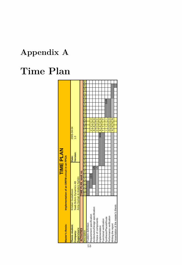
Appendix A
Time PlanSu
perv
isor
s:A
nna
Gom
an &
And
ers
Nyh
lén
1011
1213
1415
1617
1819
2021
2223
2425
2627
2829
3031
3233
3435
3637
3839
40
VV
VV
AA
AA
CC
CC
AA
AA
TT
TT
II
II
OO
OO
NN
NN
31/8
TIM
E PL
AN
Mas
ter's
thes
is:
Impl
emen
tatio
n of
an
DR
FM-c
ircui
t in
an F
PGA
30/6
Per
form
ance
ver
ifica
tion
15/4
1/5
1/5
Cho
ice
of c
ompo
nent
sIm
plem
enta
tion
Func
tiona
l ver
ifica
tion
Syn
thes
is/P
lace
&R
oute
Writ
ing
the
repo
rtP
rese
ntat
ion
of th
e m
aste
r's th
esis
AC
TIVI
TIES
TIM
E PL
AN
, wee
k no
.D
escr
iptio
nP
robl
em d
efin
ition
Req
uire
men
t spe
cific
atio
nA
rcite
ctur
es/D
esig
n sp
ecifi
catio
n
Dat
e:Ve
rsio
n:20
05-0
4-04
1.0
Thes
is s
tude
nt:
Com
pany
:K
ristia
n G
usta
fsso
nS
aab
Bof
ors
Dyn
amic
s A
B
53
Appendix B
Requirement Specification
Saab Bofors Dynamics AB REQUIREMENT SPECIFICATION 1 (9) Utfärdare, tjänsteställe, telefon Issued by, department, telephone Datum Date Utgåva
Issue IDDokumentnummer Document ID
Kristian Gustafsson, RTEAD 2005-04-22 1.1 Godkänd av Approved by Antal bilagor
No. of appendicesInformationsklass Classification
Mottagare Addressee(s)
Anders Nylén Sture Carlson Anna Goman Ulf Malmqvist
ELSI. Requirement specification for the DRFM circuit in the TEG.
1 INTRODUCTION This requirement specification defines the demands on the DRFM circuit developed as a part of a master’s thesis at Saab Bofors Dynamics AB. The specification is intended to limit the extent of the thesis so that results can be achieved within the time planned for the thesis according to the time plan.
In this specification all the requirements will be defined in table row according to the row belov:
Req. No. X Description for requirement No. X Priority Column one states the number of the specific requirement. In column two the description of the requirement can be found. In the third column the priority of the requirement is found. Priority 1 is hard requirements that have to be fulfilled before the development of the DRFM circuit is considered finished. Priority 2 is requirements that will be fulfilled only if extra time is available when the priority 1 requirements have been fulfilled.
Saab Bofors Dynamics AB REQUIREMENT SPECIFICATION 2 (9) Utfärdare, tjänsteställe, telefon Issued by, department, telephone Datum Date Utgåva
Issue IDDokumentnummer Document ID
Kristian Gustafsson, RTEAD 2005-04-22 1.1 Godkänd av Approved by Antal bilagor
No. of appendicesInformationsklass Classification
2 ABBREVIATIONS CW Continuous Wave DRFM Digital Radio Frequency Memory ECM Electronic Countermeasure ELSI Electronic Warfare Simulator FPGA Field Programmable Gate Array JTAG Joint Test Action Group TEG Target Echo Generator PRF Pulse Repetition Frequency RF Radio Frequency VHDL VHSIC Hardware Description Language VHSIC Very High Speed Integrated Circuit
3 BACKGROUND
The DRFM circuit is a part of the TEG in the simulator ELSI. The main task of the circuit is sending radar echoes, using the radar equipments in ELSI, to the radar seeker with a delay equivalent to the distance to a simulated target. The current circuit is not able to meet the new technical requirements which the simulator has to be able to handle in the future. Also, the functions in the current design have never been fully used and a desire of new functions have arisen. These are the reasons for developing a new DRFM circuit.
Control and memory access of the circuit will be using an external computer interface. The choice of the interface will be done later on, during this thesis, or it will be done after the development of the circuit has finished. This result in that the interface specified in this document will only be a general parallel interface.
After implementation of the circuits they will be assembled on a circuit board which will be used in the simulator.
In this specification it is only the DRFM functions, the interface to the computer and the communication between the two blocks that are specified.
Req. No. 1 The circuit shall be controlled through an external computer interface.
1
Denna handling och informationen häri är Saab Bofors Dynamics AB egen- dom och får ej användas, delges obehöriga eller ändras utan Saab Bofors Dyna-mics AB skriftliga medgivande.
This document and the information contained herein is the property of Saab Bofors Dynamics AB and must not be used, disclosed or altered without Saab Bofors Dynamics AB prior written consent.
p16/allmänblankett.dot/utg5
54
55
Saab Bofors Dynamics AB REQUIREMENT SPECIFICATION 2 (9) Utfärdare, tjänsteställe, telefon Issued by, department, telephone Datum Date Utgåva
Issue IDDokumentnummer Document ID
Kristian Gustafsson, RTEAD 2005-04-22 1.1 Godkänd av Approved by Antal bilagor
No. of appendicesInformationsklass Classification
2 ABBREVIATIONS CW Continuous Wave DRFM Digital Radio Frequency Memory ECM Electronic Countermeasure ELSI Electronic Warfare Simulator FPGA Field Programmable Gate Array JTAG Joint Test Action Group TEG Target Echo Generator PRF Pulse Repetition Frequency RF Radio Frequency VHDL VHSIC Hardware Description Language VHSIC Very High Speed Integrated Circuit
3 BACKGROUND
The DRFM circuit is a part of the TEG in the simulator ELSI. The main task of the circuit is sending radar echoes, using the radar equipments in ELSI, to the radar seeker with a delay equivalent to the distance to a simulated target. The current circuit is not able to meet the new technical requirements which the simulator has to be able to handle in the future. Also, the functions in the current design have never been fully used and a desire of new functions have arisen. These are the reasons for developing a new DRFM circuit.
Control and memory access of the circuit will be using an external computer interface. The choice of the interface will be done later on, during this thesis, or it will be done after the development of the circuit has finished. This result in that the interface specified in this document will only be a general parallel interface.
After implementation of the circuits they will be assembled on a circuit board which will be used in the simulator.
In this specification it is only the DRFM functions, the interface to the computer and the communication between the two blocks that are specified.
Req. No. 1 The circuit shall be controlled through an external computer interface.
1
Denna handling och informationen häri är Saab Bofors Dynamics AB egen- dom och får ej användas, delges obehöriga eller ändras utan Saab Bofors Dyna-mics AB skriftliga medgivande.
This document and the information contained herein is the property of Saab Bofors Dynamics AB and must not be used, disclosed or altered without Saab Bofors Dynamics AB prior written consent.
p16/allmänblankett.dot/utg5
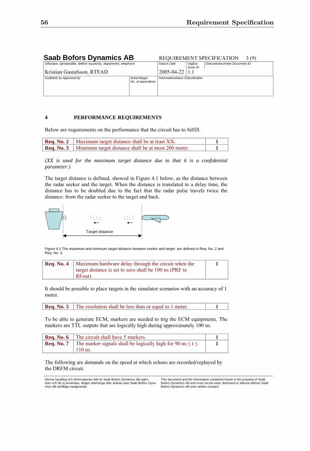
56 Requirement Specification
Saab Bofors Dynamics AB REQUIREMENT SPECIFICATION 3 (9) Utfärdare, tjänsteställe, telefon Issued by, department, telephone Datum Date Utgåva
Issue IDDokumentnummer Document ID
Kristian Gustafsson, RTEAD 2005-04-22 1.1 Godkänd av Approved by Antal bilagor
No. of appendicesInformationsklass Classification
4 PERFORMANCE REQUIREMENTS Below are requirements on the performance that the circuit has to fulfill.
Req. No. 2 Maximum target distance shall be at least XX. 1 Req. No. 3 Minimum target distance shall be at most 200 meter. 1 (XX is used for the maximum target distance due to that it is a confidential parameter.)
The target distance is defined, showed in Figure 4.1 below, as the distance between the radar seeker and the target. When the distance is translated to a delay time, the distance has to be doubled due to the fact that the radar pulse travels twice the distance: from the radar seeker to the target and back.
Target distance
Figure 4.1 The maximum and minimum target distance between seeker and target are defined in Req. No. 2 and Req. No. 3.
Req. No. 4 Maximum hardware delay through the circuit when the target distance is set to zero shall be 100 ns (PRF to RFout).
1
It should be possible to place targets in the simulator scenarios with an accuracy of 1 meter.
Req. No. 5 The resolution shall be less than or equal to 1 meter. 1 To be able to generate ECM, markers are needed to trig the ECM equipments. The markers are TTL outputs that are logically high during approximately 100 ns.
Req. No. 6 The circuit shall have 5 markers. 1 Req. No. 7 The marker signals shall be logically high for 90 ns ≤ t ≤
110 ns. 1
The following are demands on the speed at which echoes are recorded/replayed by the DRFM circuit.
Denna handling och informationen häri är Saab Bofors Dynamics AB egen- dom och får ej användas, delges obehöriga eller ändras utan Saab Bofors Dyna-mics AB skriftliga medgivande.
This document and the information contained herein is the property of Saab Bofors Dynamics AB and must not be used, disclosed or altered without Saab Bofors Dynamics AB prior written consent.
p16/allmänblankett.dot/utg5
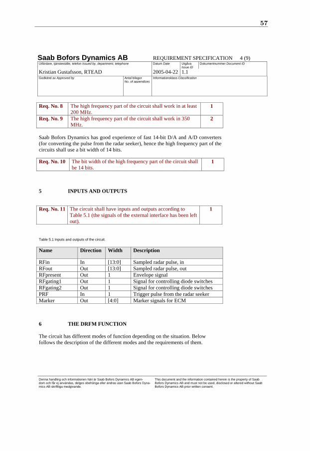
57
Saab Bofors Dynamics AB REQUIREMENT SPECIFICATION 4 (9) Utfärdare, tjänsteställe, telefon Issued by, department, telephone Datum Date Utgåva
Issue IDDokumentnummer Document ID
Kristian Gustafsson, RTEAD 2005-04-22 1.1 Godkänd av Approved by Antal bilagor
No. of appendicesInformationsklass Classification
Denna handling och informationen häri är Saab Bofors Dynamics AB egen- dom och får ej användas, delges obehöriga eller ändras utan Saab Bofors Dyna-mics AB skriftliga medgivande.
This document and the information contained herein is the property of Saab Bofors Dynamics AB and must not be used, disclosed or altered without Saab Bofors Dynamics AB prior written consent.
p16/allmänblankett.dot/utg5
Req. No. 8 The high frequency part of the circuit shall work in at least 200 MHz.
1
Req. No. 9 The high frequency part of the circuit shall work in 350 MHz.
2
Saab Bofors Dynamics has good experience of fast 14-bit D/A and A/D converters (for converting the pulse from the radar seeker), hence the high frequency part of the circuits shall use a bit width of 14 bits.
Req. No. 10
The bit width of the high frequency part of the circuit shall be 14 bits.
1
5 INPUTS AND OUTPUTS
Req. No. 11 The circuit shall have inputs and outputs according to Table 5.1 (the signals of the external interface has been left out).
1
Table 5.1 Inputs and outputs of the circuit.
Name Direction Width Description
RFin In [13:0] Sampled radar pulse, in RFout Out [13:0] Sampled radar pulse, out RFpresent Out 1 Envelope signal RFgating1 Out 1 Signal for controlling diode switches RFgating2 Out 1 Signal for controlling diode switches PRF In 1 Trigger pulse from the radar seeker Marker Out [4:0] Marker signals for ECM
6 THE DRFM FUNCTION The circuit has different modes of function depending on the situation. Below follows the description of the different modes and the requirements of them.
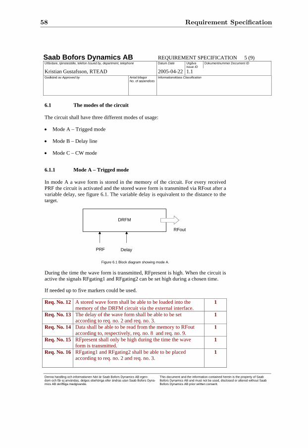
58 Requirement Specification
Saab Bofors Dynamics AB REQUIREMENT SPECIFICATION 5 (9) Utfärdare, tjänsteställe, telefon Issued by, department, telephone Datum Date Utgåva
Issue IDDokumentnummer Document ID
Kristian Gustafsson, RTEAD 2005-04-22 1.1 Godkänd av Approved by Antal bilagor
No. of appendicesInformationsklass Classification
Denna handling och informationen häri är Saab Bofors Dynamics AB egen- dom och får ej användas, delges obehöriga eller ändras utan Saab Bofors Dyna-mics AB skriftliga medgivande.
This document and the information contained herein is the property of Saab Bofors Dynamics AB and must not be used, disclosed or altered without Saab Bofors Dynamics AB prior written consent.
p16/allmänblankett.dot/utg5
6.1 The modes of the circuit The circuit shall have three different modes of usage:
• Mode A – Trigged mode
• Mode B – Delay line
• Mode C – CW mode
6.1.1 Mode A – Trigged mode In mode A a wave form is stored in the memory of the circuit. For every received PRF the circuit is activated and the stored wave form is transmitted via RFout after a variable delay, see figure 6.1. The variable delay is equivalent to the distance to the target.
DRFM
RFout
PRF Delay
Figure 6.1 Block diagram showing mode A.
During the time the wave form is transmitted, RFpresent is high. When the circuit is active the signals RFgating1 and RFgating2 can be set high during a chosen time.
If needed up to five markers could be used.
Req. No. 12 A stored wave form shall be able to be loaded into the memory of the DRFM circuit via the external interface.
1
Req. No. 13 The delay of the wave form shall be able to be set according to req. no. 2 and req. no. 3.
1
Req. No. 14 Data shall be able to be read from the memory to RFout according to, respectively, req. no. 8 and req. no. 9.
1
Req. No. 15 RFpresent shall only be high during the time the wave form is transmitted.
1
Req. No. 16 RFgating1 and RFgating2 shall be able to be placed according to req. no. 2 and req. no. 3.
1
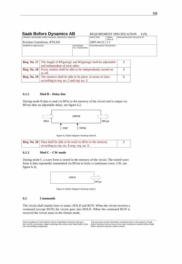
59
Saab Bofors Dynamics AB REQUIREMENT SPECIFICATION 6 (9) Utfärdare, tjänsteställe, telefon Issued by, department, telephone Datum Date Utgåva
Issue IDDokumentnummer Document ID
Kristian Gustafsson, RTEAD 2005-04-22 1.1 Godkänd av Approved by Antal bilagor
No. of appendicesInformationsklass Classification
Denna handling och informationen häri är Saab Bofors Dynamics AB egen- dom och får ej användas, delges obehöriga eller ändras utan Saab Bofors Dyna-mics AB skriftliga medgivande.
This document and the information contained herein is the property of Saab Bofors Dynamics AB and must not be used, disclosed or altered without Saab Bofors Dynamics AB prior written consent.
p16/allmänblankett.dot/utg5
Req. No. 17 The length of RFgating1 and RFgating2 shall be adjustable and independent of each other.
1
Req. No. 18 Every marker shall be able to be independently turned on or off.
1
Req. No. 19 The markers shall be able to be place, in terms of time, according to req. no. 2 and req. no. 3.
1
6.1.2 Mod B – Delay line During mode B data is read via RFin to the memory of the circuit and is output via RFout after an adjustable delay, see figure 6.2.
DRFM
RFout
Delay
RFin
PRF
Figure 6.2 Block diagram showing mode B.
Req. No. 20 Data shall be able to be read via RFin to the memory according to req. no. 8 resp. req. no. 9.
1
6.1.3 Mod C – CW mode During mode C a wave form is stored in the memory of the circuit. The stored wave form is then repeatedly transmitted via RFout to form a continuous wave, CW, see figure 6.3).
DRFM
RFout
Figure 6.3 Block diagram showing mode C.
6.2 Commands The circuit shall mainly have to states: HOLD and RUN. When the circuit receives a command (except RUN) the circuit goes into HOLD. When the command RUN is received the circuit starts in the chosen mode.
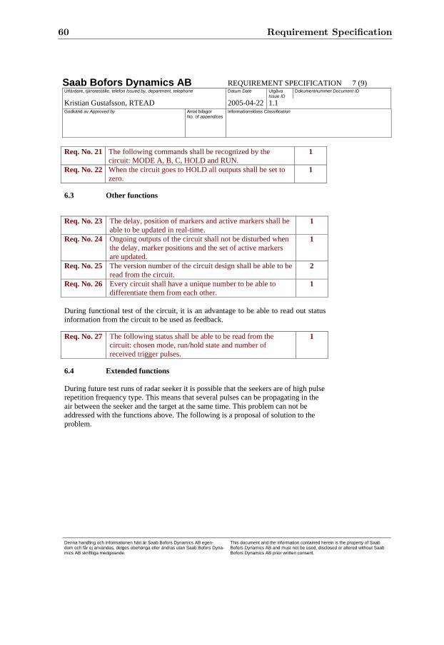
60 Requirement Specification
Saab Bofors Dynamics AB REQUIREMENT SPECIFICATION 7 (9) Utfärdare, tjänsteställe, telefon Issued by, department, telephone Datum Date Utgåva
Issue IDDokumentnummer Document ID
Kristian Gustafsson, RTEAD 2005-04-22 1.1 Godkänd av Approved by Antal bilagor
No. of appendicesInformationsklass Classification
Denna handling och informationen häri är Saab Bofors Dynamics AB egen- dom och får ej användas, delges obehöriga eller ändras utan Saab Bofors Dyna-mics AB skriftliga medgivande.
This document and the information contained herein is the property of Saab Bofors Dynamics AB and must not be used, disclosed or altered without Saab Bofors Dynamics AB prior written consent.
p16/allmänblankett.dot/utg5
Req. No. 21 The following commands shall be recognized by the circuit: MODE A, B, C, HOLD and RUN.
1
Req. No. 22 When the circuit goes to HOLD all outputs shall be set to zero.
1
6.3 Other functions
Req. No. 23 The delay, position of markers and active markers shall be able to be updated in real-time.
1
Req. No. 24 Ongoing outputs of the circuit shall not be disturbed when the delay, marker positions and the set of active markers are updated.
1
Req. No. 25 The version number of the circuit design shall be able to be read from the circuit.
2
Req. No. 26 Every circuit shall have a unique number to be able to differentiate them from each other.
1
During functional test of the circuit, it is an advantage to be able to read out status information from the circuit to be used as feedback.
Req. No. 27 The following status shall be able to be read from the circuit: chosen mode, run/hold state and number of received trigger pulses.
1
6.4 Extended functions During future test runs of radar seeker it is possible that the seekers are of high pulse repetition frequency type. This means that several pulses can be propagating in the air between the seeker and the target at the same time. This problem can not be addressed with the functions above. The following is a proposal of solution to the problem.
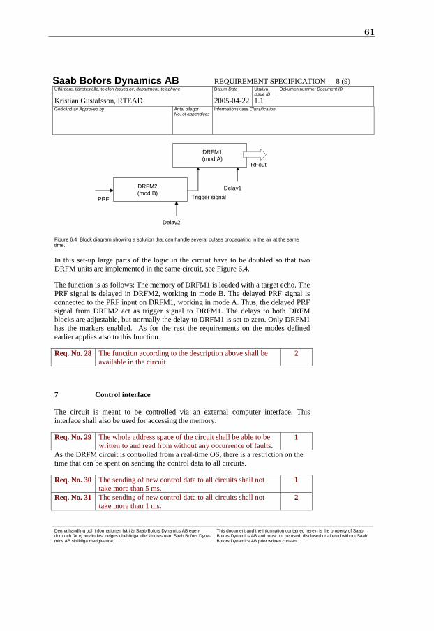
61
Saab Bofors Dynamics AB REQUIREMENT SPECIFICATION 8 (9) Utfärdare, tjänsteställe, telefon Issued by, department, telephone Datum Date Utgåva
Issue IDDokumentnummer Document ID
Kristian Gustafsson, RTEAD 2005-04-22 1.1 Godkänd av Approved by Antal bilagor
No. of appendicesInformationsklass Classification
Denna handling och informationen häri är Saab Bofors Dynamics AB egen- dom och får ej användas, delges obehöriga eller ändras utan Saab Bofors Dyna-mics AB skriftliga medgivande.
This document and the information contained herein is the property of Saab Bofors Dynamics AB and must not be used, disclosed or altered without Saab Bofors Dynamics AB prior written consent.
p16/allmänblankett.dot/utg5
DRFM1(mod A)
RFout
PRF
Delay1DRFM2(mod B)
Trigger signal
Delay2
Figure 6.4 Block diagram showing a solution that can handle several pulses propagating in the air at the same time.
In this set-up large parts of the logic in the circuit have to be doubled so that two DRFM units are implemented in the same circuit, see Figure 6.4.
The function is as follows: The memory of DRFM1 is loaded with a target echo. The PRF signal is delayed in DRFM2, working in mode B. The delayed PRF signal is connected to the PRF input on DRFM1, working in mode A. Thus, the delayed PRF signal from DRFM2 act as trigger signal to DRFM1. The delays to both DRFM blocks are adjustable, but normally the delay to DRFM1 is set to zero. Only DRFM1 has the markers enabled. As for the rest the requirements on the modes defined earlier applies also to this function.
Req. No. 28 The function according to the description above shall be available in the circuit.
2
7 Control interface The circuit is meant to be controlled via an external computer interface. This interface shall also be used for accessing the memory.
Req. No. 29 The whole address space of the circuit shall be able to be written to and read from without any occurrence of faults.
1
As the DRFM circuit is controlled from a real-time OS, there is a restriction on the time that can be spent on sending the control data to all circuits.
Req. No. 30 The sending of new control data to all circuits shall not take more than 5 ms.
1
Req. No. 31 The sending of new control data to all circuits shall not take more than 1 ms.
2
62 Requirement Specification
Saab Bofors Dynamics AB REQUIREMENT SPECIFICATION 9 (9) Utfärdare, tjänsteställe, telefon Issued by, department, telephone Datum Date Utgåva
Issue IDDokumentnummer Document ID
Kristian Gustafsson, RTEAD 2005-04-22 1.1 Godkänd av Approved by Antal bilagor
No. of appendicesInformationsklass Classification
Denna handling och informationen häri är Saab Bofors Dynamics AB egen- dom och får ej användas, delges obehöriga eller ändras utan Saab Bofors Dyna-mics AB skriftliga medgivande.
This document and the information contained herein is the property of Saab Bofors Dynamics AB and must not be used, disclosed or altered without Saab Bofors Dynamics AB prior written consent.
p16/allmänblankett.dot/utg5
8 IMPLEMENTATION
Req. No. 32 The circuit shall be implemented in an FPGA from Xilinx. 1 Req. No. 33 The FPGA shall be able to be updated via JTAG. 1 Req. No. 34 VHDL shall be used as the hardware description language. 1
9 VERIFICATION
Req. No. 35 After implementation the design shall be able to meet all priority 1 requirements in a post-Place&Route simulation.
1
Appendix C
Design Specification
Saab Bofors Dynamics AB DESIGN SPECIFICATION 1 (14) Utfärdare, tjänsteställe, telefon Issued by, department, telephone Datum Date Utgåva
Issue IDDokumentnummer Document ID
Kristian Gustafsson [xkrgu], RTEAD 2005-05-02 1.1 Godkänd av Approved by Antal bilagor
No. of appendicesInformationsklass Classification
Denna handling och informationen häri är Saab Bofors Dynamics AB egen- dom och får ej användas, delges obehöriga eller ändras utan Saab Bofors Dyna-mics AB skriftliga medgivande.
This document and the information contained herein is the property of Saab Bofors Dynamics AB and must not be used, disclosed or altered without Saab Bofors Dynamics AB prior written consent.
p16/allmänblankett.dot/utg5
Mottagare Addressee(s)
Anna Goman Ulf Malmqvist Anders Nyhlén Sture Carlsson
ELSI. Design specification for the DRFM circuit in the TEG.
63
64 Design Specification
Saab Bofors Dynamics AB DESIGN SPECIFICATION 2 (14) Utfärdare, tjänsteställe, telefon Issued by, department, telephone Datum Date Utgåva
Issue IDDokumentnummer Document ID
Kristian Gustafsson [xkrgu], RTEAD 2005-05-02 1.1 Godkänd av Approved by Antal bilagor
No. of appendicesInformationsklass Classification
Denna handling och informationen häri är Saab Bofors Dynamics AB egen- dom och får ej användas, delges obehöriga eller ändras utan Saab Bofors Dyna-mics AB skriftliga medgivande.
This document and the information contained herein is the property of Saab Bofors Dynamics AB and must not be used, disclosed or altered without Saab Bofors Dynamics AB prior written consent.
p16/allmänblankett.dot/utg5
1 INTRODUCTION...........................................................................................................3
2 ABBREVIATIONS .........................................................................................................3
3 BACKGROUND .............................................................................................................3
4 FUNCTION .....................................................................................................................4
4.1 INPUTS AND OUTPUTS ...................................................................................................4 4.1.1 MODE A – TRIGGED MODE..........................................................................................4 4.1.2 MODE B – DELAY LINE ...............................................................................................5 4.1.3 MODE C – CW MODE ..................................................................................................5
5 OVERVIEW....................................................................................................................6
6 BLOCK 1: DUAL-PORT MEMORY ...........................................................................6
6.1 BLOCKRAM..................................................................................................................7 6.2 THE IMPLEMENTATION OF THE MEMORY...................................................................7
7 BLOCK 2: CONTROL LOGIC ....................................................................................8
7.1 THE CONTENTS OF THE CONTROL LOGIC ...................................................................8 7.1.1 REGISTERS...................................................................................................................9 7.1.2 THE COUNTERS..........................................................................................................12 7.2 OPERATION DURING THE RESPECTIVE MODE...........................................................12 7.2.1 MODE A.....................................................................................................................13 7.2.2 MODE B.....................................................................................................................13 7.2.3 MODE C.....................................................................................................................14
8 BLOCK 3: EXTERNAL COMPUTER INTERFACE ..............................................14
9 HARDWARE ................................................................................................................14
65
Saab Bofors Dynamics AB DESIGN SPECIFICATION 3 (14) Utfärdare, tjänsteställe, telefon Issued by, department, telephone Datum Date Utgåva
Issue IDDokumentnummer Document ID
Kristian Gustafsson [xkrgu], RTEAD 2005-05-02 1.1 Godkänd av Approved by Antal bilagor
No. of appendicesInformationsklass Classification
Denna handling och informationen häri är Saab Bofors Dynamics AB egen- dom och får ej användas, delges obehöriga eller ändras utan Saab Bofors Dyna-mics AB skriftliga medgivande.
This document and the information contained herein is the property of Saab Bofors Dynamics AB and must not be used, disclosed or altered without Saab Bofors Dynamics AB prior written consent.
p16/allmänblankett.dot/utg5
1 INTRODUCTION A DRFM circuit is to be developed as a part of a master’s thesis at Saab Bofors Dynamics AB in Linköping. This document specifies the design of the circuit.
2 ABBREVIATIONS CW Continuous Wave DRFM Digital Radio Frequency Memory ELSI Electronic warfare simulator LVDS Low Voltage Differential Signaling TEG Target Echo Generator VME Versa Module Europe
3 BACKGROUND The DRFM circuit is a part of the TEG in ELSI. The main function of the circuit is to send target radar echoes, via radar equipments, to the radar seeker under test in the simulator. The radar echoes are delayed in the circuit for a period of time corresponding to the distance to the target. The present circuit can not handle new technical requirements on the simulator, see the requirement specification. Also, the functions in the current design have never been fully used and a desire of new func-tions has arisen. These are the reasons for developing a new DRFM circuit.
Control and memory access of the circuit will be using an external computer interface. The choice of the interface will be done later on, during this thesis, or it will be done after the development of the circuit has finished. This result in that the interface specified in this document will only be a general parallel interface.
In this specification it is only the DRFM functions, the interface to the computer and the communication between the two blocks that are specified.
66 Design Specification
Saab Bofors Dynamics AB DESIGN SPECIFICATION 4 (14) Utfärdare, tjänsteställe, telefon Issued by, department, telephone Datum Date Utgåva
Issue IDDokumentnummer Document ID
Kristian Gustafsson [xkrgu], RTEAD 2005-05-02 1.1 Godkänd av Approved by Antal bilagor
No. of appendicesInformationsklass Classification
Denna handling och informationen häri är Saab Bofors Dynamics AB egen- dom och får ej användas, delges obehöriga eller ändras utan Saab Bofors Dyna-mics AB skriftliga medgivande.
This document and the information contained herein is the property of Saab Bofors Dynamics AB and must not be used, disclosed or altered without Saab Bofors Dynamics AB prior written consent.
p16/allmänblankett.dot/utg5
4 FUNCTION The circuit has three different functions, working modes. These three are:
• Mode A – Trigged mode
• Mode B – Delay line
• Mode C – CW mode
For every mode, different inputs and output are associated. These are described in detail in the next section.
4.1 Inputs and outputs The following inputs and outputs are implemented in the circuit. (The ports associated to the computer interface are excluded.)
Table 4.1 Inputs and outputs.
Name Direction Width Description Mode
RFin In [13:0] Sampled radar pulse, in B RFout Out [13:0] Sampled radar pulse, out A, B, C RFpresent Out 1 Envelope signal A RFgating1 Out 1 Signal for controlling diode switches A RFgating2 Out 1 Signal for controlling diode switches A PRF In 1 Trigger pulse from radar seeker A, B Marker Out [4:0] Marker signals for ECM A
4.1.1 Mode A – Trigged mode In mode A a wave form is stored in the memory of the circuit. For every received PRF the circuit is activated and the stored wave form is transmitted via RFout after a variable delay, see figure 4.1. The variable delay is equivalent to the distance to the target.
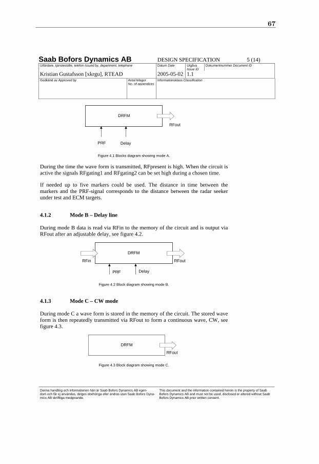
67
Saab Bofors Dynamics AB DESIGN SPECIFICATION 5 (14) Utfärdare, tjänsteställe, telefon Issued by, department, telephone Datum Date Utgåva
Issue IDDokumentnummer Document ID
Kristian Gustafsson [xkrgu], RTEAD 2005-05-02 1.1 Godkänd av Approved by Antal bilagor
No. of appendicesInformationsklass Classification
Denna handling och informationen häri är Saab Bofors Dynamics AB egen- dom och får ej användas, delges obehöriga eller ändras utan Saab Bofors Dyna-mics AB skriftliga medgivande.
This document and the information contained herein is the property of Saab Bofors Dynamics AB and must not be used, disclosed or altered without Saab Bofors Dynamics AB prior written consent.
p16/allmänblankett.dot/utg5
DRFM
RFout
PRF Delay
Figure 4.1 Blocks diagram showing mode A.
During the time the wave form is transmitted, RFpresent is high. When the circuit is active the signals RFgating1 and RFgating2 can be set high during a chosen time.
If needed up to five markers could be used. The distance in time between the markers and the PRF-signal corresponds to the distance between the radar seeker under test and ECM targets.
4.1.2 Mode B – Delay line During mode B data is read via RFin to the memory of the circuit and is output via RFout after an adjustable delay, see figure 4.2.
DRFM
RFout
Delay
RFin
PRF
Figure 4.2 Block diagram showing mode B.
4.1.3 Mode C – CW mode During mode C a wave form is stored in the memory of the circuit. The stored wave form is then repeatedly transmitted via RFout to form a continuous wave, CW, see figure 4.3.
DRFM
RFout
Figure 4.3 Block diagram showing mode C.
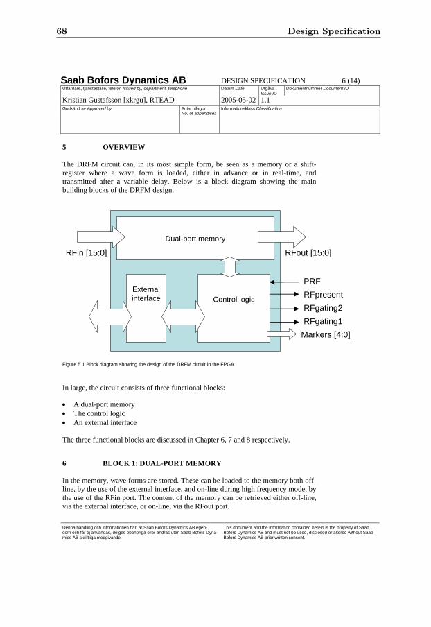
68 Design Specification
Saab Bofors Dynamics AB DESIGN SPECIFICATION 6 (14) Utfärdare, tjänsteställe, telefon Issued by, department, telephone Datum Date Utgåva
Issue IDDokumentnummer Document ID
Kristian Gustafsson [xkrgu], RTEAD 2005-05-02 1.1 Godkänd av Approved by Antal bilagor
No. of appendicesInformationsklass Classification
Denna handling och informationen häri är Saab Bofors Dynamics AB egen- dom och får ej användas, delges obehöriga eller ändras utan Saab Bofors Dyna-mics AB skriftliga medgivande.
This document and the information contained herein is the property of Saab Bofors Dynamics AB and must not be used, disclosed or altered without Saab Bofors Dynamics AB prior written consent.
p16/allmänblankett.dot/utg5
5 OVERVIEW The DRFM circuit can, in its most simple form, be seen as a memory or a shift-register where a wave form is loaded, either in advance or in real-time, and transmitted after a variable delay. Below is a block diagram showing the main building blocks of the DRFM design.
Dual-port memory
Externalinterface Control logic
RFout [15:0]RFin [15:0]
PRF
Markers [4:0]RFgating1RFgating2RFpresent
Figure 5.1 Block diagram showing the design of the DRFM circuit in the FPGA.
In large, the circuit consists of three functional blocks:
• A dual-port memory • The control logic • An external interface The three functional blocks are discussed in Chapter 6, 7 and 8 respectively.
6 BLOCK 1: DUAL-PORT MEMORY In the memory, wave forms are stored. These can be loaded to the memory both off-line, by the use of the external interface, and on-line during high frequency mode, by the use of the RFin port. The content of the memory can be retrieved either off-line, via the external interface, or on-line, via the RFout port.
69
Saab Bofors Dynamics AB DESIGN SPECIFICATION 7 (14) Utfärdare, tjänsteställe, telefon Issued by, department, telephone Datum Date Utgåva
Issue IDDokumentnummer Document ID
Kristian Gustafsson [xkrgu], RTEAD 2005-05-02 1.1 Godkänd av Approved by Antal bilagor
No. of appendicesInformationsklass Classification
Denna handling och informationen häri är Saab Bofors Dynamics AB egen- dom och får ej användas, delges obehöriga eller ändras utan Saab Bofors Dyna-mics AB skriftliga medgivande.
This document and the information contained herein is the property of Saab Bofors Dynamics AB and must not be used, disclosed or altered without Saab Bofors Dynamics AB prior written consent.
p16/allmänblankett.dot/utg5
Because of the fact that the memory has to work as a delay line and, thus, has to be able to be written to and read from at the same time, a dual-port memory is needed. A dual-port memory has two memory ports that can access the memory at the same time and independently from each other. Xilinx has hardware support for dual-port memory in the Virtex-4 FPGAs. These integrated memory blocks are called BlockRAM, or short BRAM.
6.1 BlockRAM A BRAM is only 18 Kbit, but several blocks can be combined to form larger memory areas. To aid the design of such larger memory areas Xilinx provides a tool called Xilinx CORE Generator (Coregen). Coregen takes parameters as inputs to generate the wanted memory. The BRAMs are possible to clock in up to 500 MHz.
6.2 The implementation of the memory With the aid of Coregen, a memory is generated with two 14-bit memory ports. The length of the memory is set according to the requirement specification. The data input of port A is connected to RFin and the data output of port B is connected to RFout. This way the memory can be both read and written to at the same time. The port A output and the port B output is used for connecting the memory to the control logic so that the memory can be read and written from the external interface. The memory is clocked according to the requirement specification to be able to meet the requirements on precision needed.
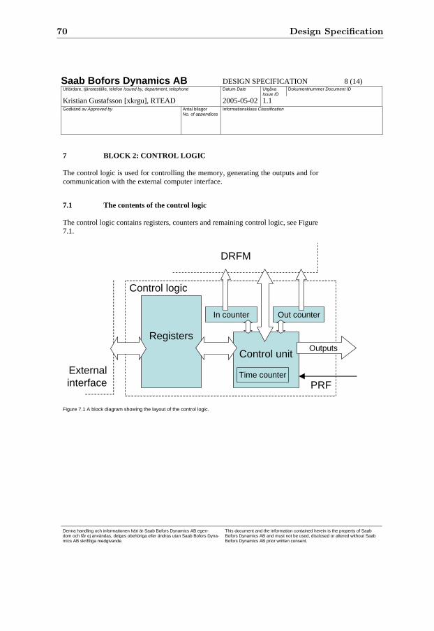
70 Design Specification
Saab Bofors Dynamics AB DESIGN SPECIFICATION 8 (14) Utfärdare, tjänsteställe, telefon Issued by, department, telephone Datum Date Utgåva
Issue IDDokumentnummer Document ID
Kristian Gustafsson [xkrgu], RTEAD 2005-05-02 1.1 Godkänd av Approved by Antal bilagor
No. of appendicesInformationsklass Classification
Denna handling och informationen häri är Saab Bofors Dynamics AB egen- dom och får ej användas, delges obehöriga eller ändras utan Saab Bofors Dyna-mics AB skriftliga medgivande.
This document and the information contained herein is the property of Saab Bofors Dynamics AB and must not be used, disclosed or altered without Saab Bofors Dynamics AB prior written consent.
p16/allmänblankett.dot/utg5
7 BLOCK 2: CONTROL LOGIC The control logic is used for controlling the memory, generating the outputs and for communication with the external computer interface.
7.1 The contents of the control logic The control logic contains registers, counters and remaining control logic, see Figure 7.1.
Registers
In counter Out counter
Control unit Outputs
Externalinterface
DRFM
PRF
Control logic
Time counter
Figure 7.1 A block diagram showing the layout of the control logic.
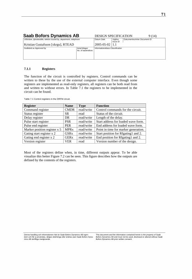
71
Saab Bofors Dynamics AB DESIGN SPECIFICATION 9 (14) Utfärdare, tjänsteställe, telefon Issued by, department, telephone Datum Date Utgåva
Issue IDDokumentnummer Document ID
Kristian Gustafsson [xkrgu], RTEAD 2005-05-02 1.1 Godkänd av Approved by Antal bilagor
No. of appendicesInformationsklass Classification
Denna handling och informationen häri är Saab Bofors Dynamics AB egen- dom och får ej användas, delges obehöriga eller ändras utan Saab Bofors Dyna-mics AB skriftliga medgivande.
This document and the information contained herein is the property of Saab Bofors Dynamics AB and must not be used, disclosed or altered without Saab Bofors Dynamics AB prior written consent.
p16/allmänblankett.dot/utg5
7.1.1 Registers The function of the circuit is controlled by registers. Control commands can be written to these by the use of the external computer interface. Even though some registers are implemented as read-only registers, all registers can be both read from and written to without errors. In Table 7.1 the registers to be implemented in the circuit can be found.
Table 7.1 Control registers in the DRFM circuit.
Register Name Type Function Command register CMDR read/write Control commands for the circuit. Status register SR read Status of the circuit. Delay register DR read/write Length of the delay. Pulse start register PSR read/write Start address for loaded wave form. Pulse end register PER read/write End address for loaded wave form. Marker position register x 5 MPRx read/write Point in time for marker generation.Gating start register x 2 GSRx read/write Start position for Rfgating1 and 2. Gating end register x 2 GERx read/write End position for Rfgating1 and 2. Version register VER read Version number of the design.
Most of the registers define when, in time, different outputs appear. To be able visualize this better Figure 7.2 can be seen. This figure describes how the outputs are defined by the contents of the registers.
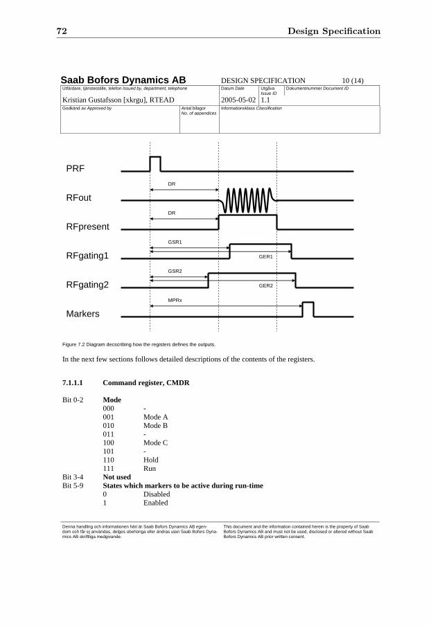
72 Design Specification
Saab Bofors Dynamics AB DESIGN SPECIFICATION 10 (14) Utfärdare, tjänsteställe, telefon Issued by, department, telephone Datum Date Utgåva
Issue IDDokumentnummer Document ID
Kristian Gustafsson [xkrgu], RTEAD 2005-05-02 1.1 Godkänd av Approved by Antal bilagor
No. of appendicesInformationsklass Classification
Denna handling och informationen häri är Saab Bofors Dynamics AB egen- dom och får ej användas, delges obehöriga eller ändras utan Saab Bofors Dyna-mics AB skriftliga medgivande.
This document and the information contained herein is the property of Saab Bofors Dynamics AB and must not be used, disclosed or altered without Saab Bofors Dynamics AB prior written consent.
p16/allmänblankett.dot/utg5
PRF
RFpresent
RFgating1
RFgating2
Markers
RFoutDR
DR
GER1
GSR2
GSR1
GER2
MPRx
Figure 7.2 Diagram decscribing how the registers defines the outputs.
In the next few sections follows detailed descriptions of the contents of the registers.
7.1.1.1 Command register, CMDR Bit 0-2 Mode 000 - 001 Mode A 010 Mode B 011 - 100 Mode C 101 - 110 Hold 111 Run Bit 3-4 Not used Bit 5-9 States which markers to be active during run-time 0 Disabled 1 Enabled
73
Saab Bofors Dynamics AB DESIGN SPECIFICATION 11 (14) Utfärdare, tjänsteställe, telefon Issued by, department, telephone Datum Date Utgåva
Issue IDDokumentnummer Document ID
Kristian Gustafsson [xkrgu], RTEAD 2005-05-02 1.1 Godkänd av Approved by Antal bilagor
No. of appendicesInformationsklass Classification
Denna handling och informationen häri är Saab Bofors Dynamics AB egen- dom och får ej användas, delges obehöriga eller ändras utan Saab Bofors Dyna-mics AB skriftliga medgivande.
This document and the information contained herein is the property of Saab Bofors Dynamics AB and must not be used, disclosed or altered without Saab Bofors Dynamics AB prior written consent.
p16/allmänblankett.dot/utg5
Bit 10-16 Not used
7.1.1.2 Status register, SR Bit 0-2 Chosen mode 000 - 001 Mode A 010 Mode B 011 - 100 Mode C 101 - 110 - 111 - Bit 3 State of circuit 0 Run 1 Hold Bit 4-5 State of the finite state machine in the control logic block 00 Wait 01 Active 10 Load 11 Update Bit 4-16 PRF counter The number of PRF pulses received by the circuit since last reset.
7.1.1.3 Delay register, DR The number of clock periods to delay the signal.
7.1.1.4 Pulse start register, PSR The start address of the wave form stored in the memory.
7.1.1.5 Pulse end register, PER The end address of the wave form stored in the memory.
74 Design Specification
Saab Bofors Dynamics AB DESIGN SPECIFICATION 12 (14) Utfärdare, tjänsteställe, telefon Issued by, department, telephone Datum Date Utgåva
Issue IDDokumentnummer Document ID
Kristian Gustafsson [xkrgu], RTEAD 2005-05-02 1.1 Godkänd av Approved by Antal bilagor
No. of appendicesInformationsklass Classification
Denna handling och informationen häri är Saab Bofors Dynamics AB egen- dom och får ej användas, delges obehöriga eller ändras utan Saab Bofors Dyna-mics AB skriftliga medgivande.
This document and the information contained herein is the property of Saab Bofors Dynamics AB and must not be used, disclosed or altered without Saab Bofors Dynamics AB prior written consent.
p16/allmänblankett.dot/utg5
7.1.1.6 Marker register, MPR1 – MPR5 The number of clock periods after the PRF to wait before generation of the marker signal.
7.1.1.7 Gating start register, GSR1 and GSR2 The start position of the gating signals in terms of clock periods after the PRF pulse.
7.1.1.8 Gating end register, GER1 and GER2 The end position of the gating signals in terms of clock periods after the PRF pulse.
7.1.1.9 Version register, VER The version number of the DRFM design.
7.1.2 The counters The time counter (TC) is an up counter, clocked with the same clock as the memory, that is activated by the PRF pulse after which it counts up continuously until all outputs have been generated.
The in counter (IC) and out counter (OC) are up-counters addressing the memory. IC addresses where data on the RFin port should be written to and OC addresses where data should be read from to the RFout port. The counters are loaded with the appropriate values, depending on mode, and are clocked with the same clock as the memory.
7.2 Operation during the respective mode The circuit should behave differently in the different modes, therefore the control logic also has to behave different depending on mode. Below follows a description of how the logic should act in the respective modes.
75
Saab Bofors Dynamics AB DESIGN SPECIFICATION 13 (14) Utfärdare, tjänsteställe, telefon Issued by, department, telephone Datum Date Utgåva
Issue IDDokumentnummer Document ID
Kristian Gustafsson [xkrgu], RTEAD 2005-05-02 1.1 Godkänd av Approved by Antal bilagor
No. of appendicesInformationsklass Classification
Denna handling och informationen häri är Saab Bofors Dynamics AB egen- dom och får ej användas, delges obehöriga eller ändras utan Saab Bofors Dyna-mics AB skriftliga medgivande.
This document and the information contained herein is the property of Saab Bofors Dynamics AB and must not be used, disclosed or altered without Saab Bofors Dynamics AB prior written consent.
p16/allmänblankett.dot/utg5
7.2.1 Mode A A wave form is loaded to the memory via the external interface, see Chapter 8. Mode A and active markers are set in CMDR. The delay is set in DR. PSR and PER are loaded with the start and end memory address of the pulse. MPRx are loaded with the values corresponding to the distance in time between the PRF pulse and the markers. GSRx and GERx are set to the start and end time for the respective gating signals. The circuit is activated by setting the RUN command in CMDR.
The read-out is performed in the following way: The external PRF pulse activates the high frequency part of the circuit. OC is loaded with the content of PSR. TC is starting to count up from zero. During the count up, TC is compared with the register contents resulting in:
• When TC becomes equal to the content in DR, the memory and OC are activated. OC counts up and addresses data in the memory which is outputted by the RFout port. During the time data is outputted RFpresent is high. When OC becomes greater then PER, all bits in RFout goes low, the memory is deactivated and RFpresent goes low.
• When TC is in the interval between GSRx and GERx, the corresponding gating signals are high.
• When TC becomes equal to MPRx maker pulses are outputted from the specified makrer ports (chosen in CMDR).
• When TC becomes greater than the register with the highest value, TC stops counting, the high frequency part of the design goes into idle state and awaits a new PRF pulse.
7.2.2 Mode B Mode B and active markers are set in CMDR. DR, MPRx, GSRx and GERx is loaded in the same way as in mode A. The circuit is activated by the RUN command in CMDR. IC and TC are set to zero. OC is loaded with –DR, i.e. the negative delay. This results in that the delay is defined as the difference between the contens of IC and OC. IC addresses the write position in the memory for data on the RFin port and OC addresses read position in the memory for data to be outputted on the RFout port. Both counters are counting up. When the counters come to the highest position in the memory they are restarted at zero again. For every received PRF, TC is set to zero and OC is loaded with the value of IC minus the content of DR. This causes the delay to be defined as the difference between IC and OC. TC is compared to the registers in the same way as in mode A to be able to generate the remaining outputs.
76 Design Specification
Saab Bofors Dynamics AB DESIGN SPECIFICATION 14 (14) Utfärdare, tjänsteställe, telefon Issued by, department, telephone Datum Date Utgåva
Issue IDDokumentnummer Document ID
Kristian Gustafsson [xkrgu], RTEAD 2005-05-02 1.1 Godkänd av Approved by Antal bilagor
No. of appendicesInformationsklass Classification
Denna handling och informationen häri är Saab Bofors Dynamics AB egen- dom och får ej användas, delges obehöriga eller ändras utan Saab Bofors Dyna-mics AB skriftliga medgivande.
This document and the information contained herein is the property of Saab Bofors Dynamics AB and must not be used, disclosed or altered without Saab Bofors Dynamics AB prior written consent.
p16/allmänblankett.dot/utg5
7.2.3 Mode C A wave form is loaded to the memory via the external computer interface. Mode C is set in CMDR. PSR and PER is loaded in the same way as in mode A. The circuit is activated by the RUN command in CMDR.
After the circuit has been activated, OC is loaded with the content in PSR and starts to count up with the specified frequency. OC addresses data in the memory and outputs it through the RFout port. When OC is equal to the content of PER OC is loaded with PSR again and starts counting up again. The result is a continuous wave form.
8 BLOCK 3: EXTERNAL COMPUTER INTERFACE The external computer interface is used for communication with the communication interface that will be chosen to accompany the circuit. Until the interface has been chosen, which will be done after this project has ended, the interface in the FPGA is implemented as a “black box” with a general parallel interface to the external world. This is done so that the external interface can be chosen later.
9 HARDWARE
The DRFM design will be implemented in a Virtex-4 FPGA developed by the American company Xilinx. The circuit will be attached on a VME circuit board and mounted in a VME rack in the TEG in ELSI.
The Virtex-4 circuit has support for LVDS signaling. This standard will be used for the ports associated with the high frequency part of the circuit, i.e. the RFin and RFout ports. The rest of the ports will be standard TTL level ports.
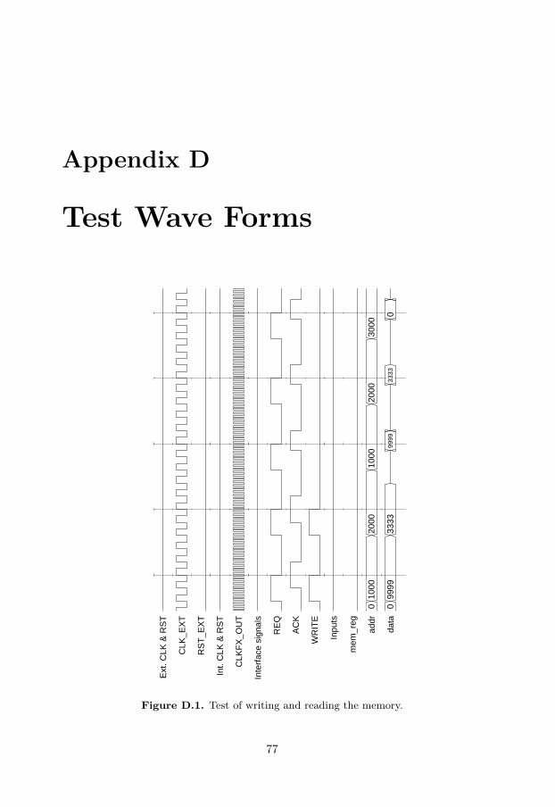
Appendix D
Test Wave Forms
Ext
. CLK
& R
ST
Int.
CLK
& R
ST
Inte
rface
sig
nals
Inpu
ts
010
0020
0010
0020
0030
000
12
34
56
099
9933
3399
9933
330
5089
112
100
5210
020
0
600
ns80
0 ns
1 us
1200
ns
1400
ns
1600
ns
Ext
. CLK
& R
ST
CLK
_EX
T
RS
T_E
XT
Int.
CLK
& R
ST
CLK
FX_O
UT
Inte
rface
sig
nals
RE
Q
AC
K
WR
ITE
Inpu
ts
mem
_reg
addr
010
0020
0010
0020
0030
000
12
34
56
data
099
9933
3399
9933
330
5089
112
100
5210
020
0
Ent
ity:to
p_ch
ip_t
b A
rchi
tect
ure:
stru
ct D
ate:
Thu
Oct
13
15:4
7:56
HD
T 20
05
Row
: 1 P
age:
1
Figure D.1. Test of writing and reading the memory.
77
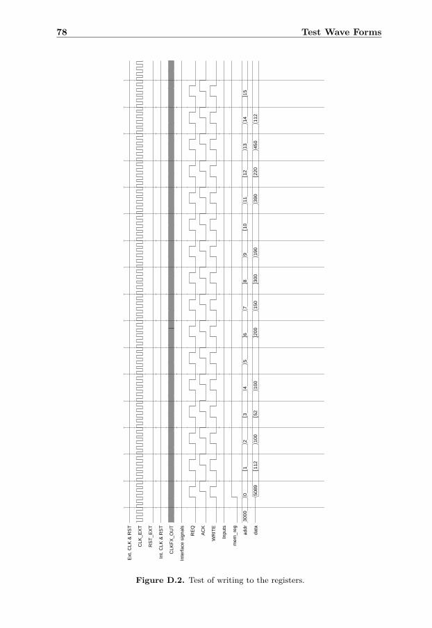
78 Test Wave Forms
Ext
. CLK
& R
ST
Int.
CLK
& R
ST
Inte
rface
sig
nals
Inpu
ts
3000
01
23
45
67
89
1011
1213
1415
5089
112
100
5210
020
015
030
019
039
022
045
011
2
1 us
1200
ns
1400
ns
1600
ns
1800
ns
2 us
2200
ns
2400
ns
2600
ns
Ext
. CLK
& R
ST
CLK
_EX
T
RS
T_E
XT
Int.
CLK
& R
ST
CLK
FX_O
UT
Inte
rface
sig
nals
RE
Q
AC
K
WR
ITE
Inpu
ts
mem
_reg
addr
3000
01
23
45
67
89
1011
1213
1415
data
5089
112
100
5210
020
015
030
019
039
022
045
011
2
Ent
ity:to
p_ch
ip_t
b A
rchi
tect
ure:
stru
ct D
ate:
Thu
Oct
13
15:1
8:31
HD
T 20
05
Row
: 1 P
age:
1
Figure D.2. Test of writing to the registers.
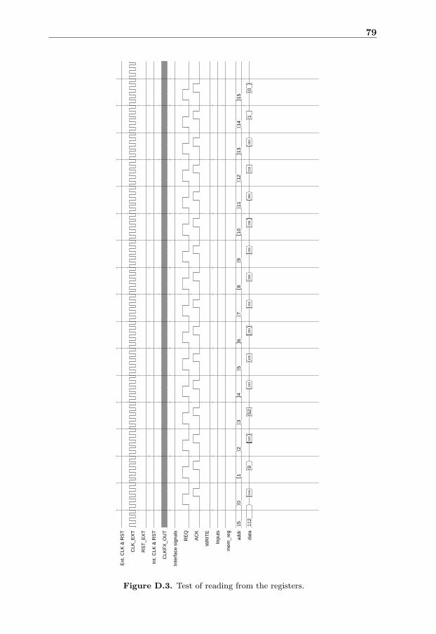
79
Ext
. CLK
& R
ST
Int.
CLK
& R
ST
Inte
rface
sig
nals
Inpu
ts
150
12
34
56
78
910
1112
1314
15
112
5089
910
052
100
100
200
150
300
190
190
390
220
450
10
2800
ns
3 us
3200
ns
3400
ns
3600
ns
3800
ns
4 us
4200
ns
Ext
. CLK
& R
ST
CLK
_EX
T
RS
T_E
XT
Int.
CLK
& R
ST
CLK
FX_O
UT
Inte
rface
sig
nals
RE
Q
AC
K
WR
ITE
Inpu
ts
mem
_reg
addr
150
12
34
56
78
910
1112
1314
15
data
112
5089
910
052
100
100
200
150
300
190
190
390
220
450
10
Ent
ity:to
p_ch
ip_t
b A
rchi
tect
ure:
stru
ct D
ate:
Thu
Oct
13
15:2
0:41
HD
T 20
05
Row
: 1 P
age:
1
Figure D.3. Test of reading from the registers.
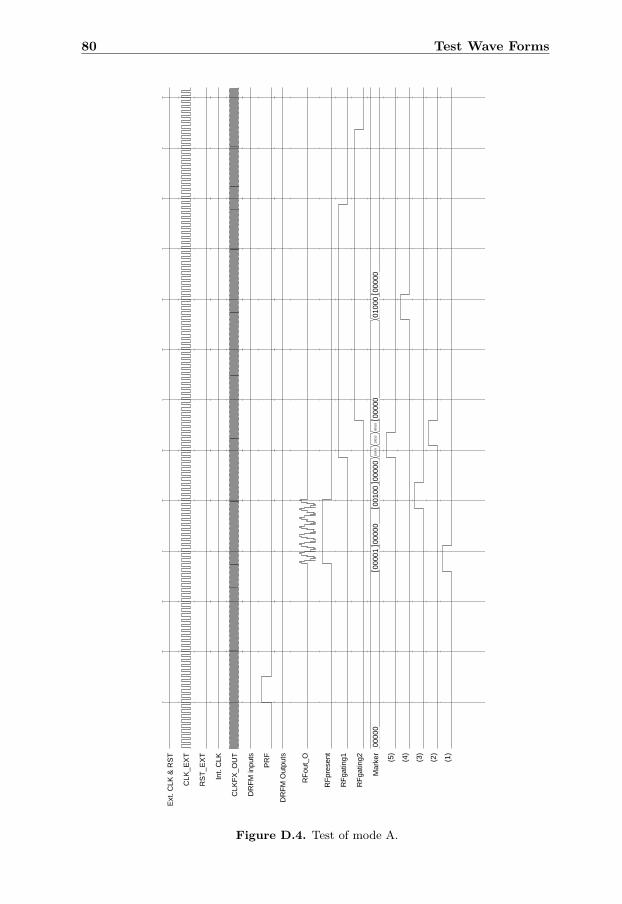
80 Test Wave Forms
Ext
. CLK
& R
ST
Int.
CLK
DR
FM in
puts
DR
FM O
utpu
ts
0000
000
001
0000
000
100
0000
010
000
1001
000
010
0000
001
000
0000
0
1250
0 ns
13 u
s13
500
ns14
us
1450
0 ns
Ext
. CLK
& R
ST
CLK
_EX
T
RS
T_E
XT
Int.
CLK
CLK
FX_O
UT
DR
FM in
puts
PR
F
DR
FM O
utpu
ts
RFo
ut_O
RFp
rese
nt
RFg
atin
g1
RFg
atin
g2
Mar
ker
0000
000
001
0000
000
100
0000
010
000
1001
000
010
0000
001
000
0000
0
(5)
(4)
(3)
(2)
(1)
Ent
ity:to
p_ch
ip_t
b A
rchi
tect
ure:
stru
ct D
ate:
Mon
Oct
10
13:3
7:55
HD
T 20
05
Row
: 1 P
age:
1
Figure D.4. Test of mode A.
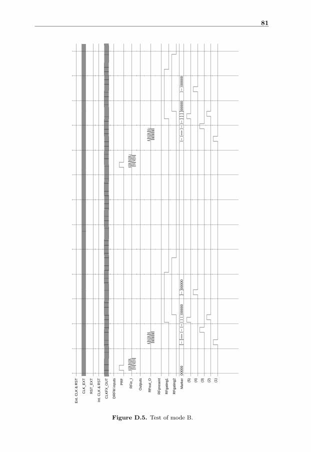
81
Ext
. CLK
& R
ST
Int.
CLK
& R
ST
DR
FM in
puts
Out
puts
0000
000
001
0000
000
100
0000
000
000
0100
000
000
0000
100
000
0010
000
000
0000
001
000
0000
0
2 us
3 us
4 us
5 us
6 us
7 us
8 us
Ext
. CLK
& R
ST
CLK
_EX
T
RS
T_E
XT
Int.
CLK
& R
ST
CLK
FX_O
UT
DR
FM in
puts
PR
F
RFi
n_I
Out
puts
RFo
ut_O
RFp
rese
nt
RFg
atin
g1
RFg
atin
g2
Mar
ker
0000
000
001
0000
000
100
0000
000
000
0100
000
000
0000
100
000
0010
000
000
0000
001
000
0000
0
(5)
(4)
(3)
(2)
(1)
Ent
ity:to
p_ch
ip_t
b A
rchi
tect
ure:
stru
ct D
ate:
Mon
Oct
10
16:2
1:28
HD
T 20
05
Row
: 1 P
age:
1
Figure D.5. Test of mode B.
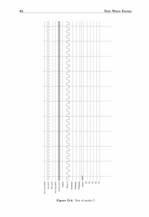
82 Test Wave Forms
Ext
. CLK
& R
ST
Int.
CLK
& R
ST
Out
puts
0000
0
18 u
s18
200
ns18
400
ns18
600
ns18
800
ns
Ext
. CLK
& R
ST
CLK
_EX
T
RS
T_E
XT
Int.
CLK
& R
ST
CLK
FX_O
UT
Out
puts
RFo
ut_O
RFp
rese
nt
RFg
atin
g1
RFg
atin
g2
Mar
ker
0000
0
(5)
(4)
(3)
(2)
(1)
Ent
ity:to
p_ch
ip_t
b A
rchi
tect
ure:
stru
ct D
ate:
Wed
Oct
12
13:1
9:11
HD
T 20
05
Row
: 1 P
age:
1
Figure D.6. Test of mode C.
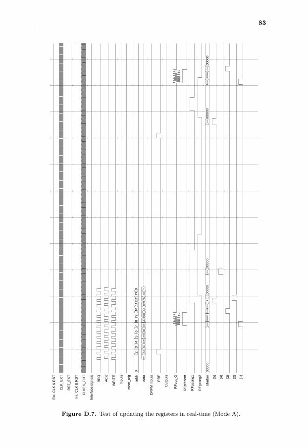
83
Ext
. CLK
& R
ST
Int.
CLK
& R
ST
Inte
rface
sig
nals
Inpu
ts
02
34
56
78
910
1112
130
5095
200
5010
020
050
250
3050
100
150
7522
567
9
DR
FM in
puts
Out
puts
0000
000
001
0000
000
100
0000
000
000
0100
000
000
1000
000
000
0000
100
000
0010
000
000
21 u
s22
us
23 u
s24
us
25 u
s26
us
Ext
. CLK
& R
ST
CLK
_EX
T
RS
T_E
XT
Int.
CLK
& R
ST
CLK
FX_O
UT
Inte
rface
sig
nals
RE
Q
AC
K
WR
ITE
Inpu
ts
mem
_reg
addr
02
34
56
78
910
1112
130
data
5095
200
5010
020
050
250
3050
100
150
7522
567
9
DR
FM in
puts
PR
F
Out
puts
RFo
ut_O
RFp
rese
nt
RFg
atin
g1
RFg
atin
g2
Mar
ker
0000
000
001
0000
000
100
0000
000
000
0100
000
000
1000
000
000
0000
100
000
0010
000
000
(5)
(4)
(3)
(2)
(1)
Ent
ity:to
p_ch
ip_t
b A
rchi
tect
ure:
stru
ct D
ate:
Fri
Oct
14
14:4
3:27
HD
T 20
05
Row
: 1 P
age:
1
Figure D.7. Test of updating the registers in real-time (Mode A).
På svenska
Detta dokument hålls tillgängligt på Internet – eller dess framtida ersättare –under en längre tid från publiceringsdatum under förutsättning att inga extra-ordinära omständigheter uppstår.
Tillgång till dokumentet innebär tillstånd för var och en att läsa, ladda ner,skriva ut enstaka kopior för enskilt bruk och att använda det oförändrat för ick-ekommersiell forskning och för undervisning. Överföring av upphovsrätten viden senare tidpunkt kan inte upphäva detta tillstånd. All annan användning avdokumentet kräver upphovsmannens medgivande. För att garantera äktheten,säkerheten och tillgängligheten finns det lösningar av teknisk och administrativart.Upphovsmannens ideella rätt innefattar rätt att bli nämnd som upphovsman i denomfattning som god sed kräver vid användning av dokumentet på ovan beskrivnasätt samt skydd mot att dokumentet ändras eller presenteras i sådan form eller isådant sammanhang som är kränkande för upphovsmannens litterära eller konst-närliga anseende eller egenart.
För ytterligare information om Linköping University Electronic Press se för-lagets hemsidahttp://www.ep.liu.se/
In English
The publishers will keep this document online on the Internet - or its possiblereplacement - for a considerable time from the date of publication barring excep-tional circumstances.
The online availability of the document implies a permanent permission foranyone to read, to download, to print out single copies for your own use and touse it unchanged for any non-commercial research and educational purpose. Sub-sequent transfers of copyright cannot revoke this permission. All other uses ofthe document are conditional on the consent of the copyright owner. The pub-lisher has taken technical and administrative measures to assure authenticity,security and accessibility.
According to intellectual property law the author has the right to be men-tioned when his/her work is accessed as described above and to be protectedagainst infringement.
For additional information about the Linköping University Electronic Pressand its procedures for publication and for assurance of document integrity, pleaserefer to its WWW home page:http://www.ep.liu.se/
© Kristian Gustafsson