
AVR CPU Core & 8 bit AVR Instruction Set. incoming Lab. 안철수 KAIST 석좌교수 " 개발자가...
32
AVR CPU Core & 8 bit AVR Instruction Set
-
Upload
jack-bridges -
Category
Documents
-
view
225 -
download
3
Transcript of AVR CPU Core & 8 bit AVR Instruction Set. incoming Lab. 안철수 KAIST 석좌교수 " 개발자가...
AVR CPU Core & 8 bit AVR Instruction Set

incoming Lab.incoming Lab.
안철수 KAIST 석좌교수 " 개발자가 성공하는 길 "
개발자가 성공하는 길
http://www.devmento.co.kr/devmain/ucc/ucc/ucc_detail.jsp?cate_code=ADAFAA&dataSeq=76&main_id=SUCC1W001

incoming Lab.incoming Lab.
Block Diagram of the AVR Architecture
incoming Lab.incoming Lab.
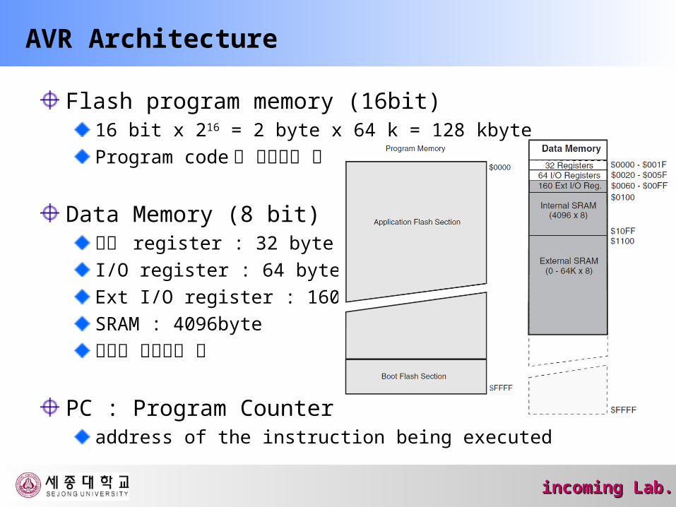
AVR Architecture
Flash program memory (16bit)16 bit x 216 = 2 byte x 64 k = 128 kbyteProgram code 가 저장되는 곳
Data Memory (8 bit)범용 register : 32 byteI/O register : 64 byteExt I/O register : 160 byteSRAM : 4096byte변수가 저장되는 곳
PC : Program Counteraddress of the instruction being executed

incoming Lab.incoming Lab.
Program / Compile / Execution
Program 작성 -> C code 생성Compile -> hex code 생성
hex code : download 가 가능한 codemachine code (opcode) : 실행 가능한 codeassembly code : machine code 의 의미
Executionstart address of program code => PCFetch : PC -> flash program memory => machine code -> IR
PC = PC+1 ( 또는 PC+2) (IR : instruction register)Decode : instruction decodeRegister Operand Fetch ALU Operation Execute Result Write Backgoto Fetch

incoming Lab.incoming Lab.
Instruction Execution
Instructionan element of an executable program a single operation of a processor
Parallel Instruction Fetches and Instruction ExecutionsSingle Clock Cycle Execution : Harvard architecture
clkCPU : system clock Atmega 128 : 16MHz 가능 , XTAL1 pin 으로 공급실습 kit : 7.3728 MHz ( 확인요 )

incoming Lab.incoming Lab.
Single Cycle ALU Operation (in AVR)
Execution Cycle
Execution Time 1/clkCPU
clkCPU = 16 MHz ?
clkCPU = 7.3728 MHz ?

incoming Lab.incoming Lab.
8 bit AVR Instruction Set
AVR Instruction Set : http://www.atmel.com133 InstructionsInstruction
Operation Code + Operand
Operation Code : ALU 가 실행할 내용Operand : ALU 가 실행할 대상Ex) ADC : Add with Carry
‘ADC R1, R2’ 의 opcode 는 ?

incoming Lab.incoming Lab.
Operation Code 의 유형
Arithmetic and Logic범용 레지스터간의 사칙연산과 로직 연산ADC, AND, SUB, AND, OR, …
Branch Change program counter : 다른 opcode 위치로 이동JMP, BRBC, …
Data TransferLoad : SRAM 등의 Data 를 범용 Register 로 이동 (LD, LDI, …)Store : 범용 Register 의 값을 SRAM 등으로 이동 (ST, STD, …)
Bit and Bit-TestRegister 의 특정 bit 을 set(=‘1’) 하거나 clear(=‘0’) 으로 변경SBI, CLI, ….
MCU Control

incoming Lab.incoming Lab.
Data Addressing Mode : Operand 의 유형
Immediateactual operand
Direct (absolute)address of operand Register Direct, I/O Direct, Data Direct
IndirectAddress that specifies (or points to ) operand Data Indirect, Data Indirect with Displacement, Data Indirect with Pre-Decrement, Data Indirect with Post-Increment

incoming Lab.incoming Lab.
Example) Immediate Addressing
ANDI – Logical AND with Immediate
ANDI r17, $0F

incoming Lab.incoming Lab.
Example) Register Direct Addressing

incoming Lab.incoming Lab.
Example) Register Direct Addressing
ADD – Add without Carry
ADD r1, r2ADD r28, r28
incoming Lab.incoming Lab.
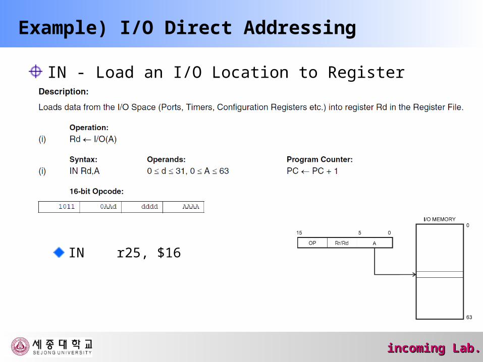
Example) I/O Direct Addressing
IN - Load an I/O Location to Register
IN r25, $16

incoming Lab.incoming Lab.
Example) Data Direct Addressing
LDS – Load Direct from Data Space
LDS R25, $0100
2 word/2 cycle
incoming Lab.incoming Lab.
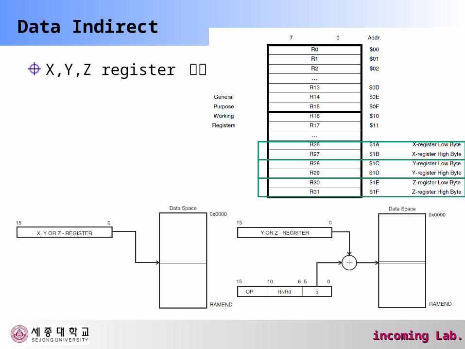
Data Indirect
X,Y,Z register 사용

incoming Lab.incoming Lab.
Example) Data Indirect
LD

incoming Lab.incoming Lab.
Example) Data Indirect
CLR R27LDI R26,$60LD R0,X+LD R1,XLDI R26,$63LD R2,XLD R3,–X

incoming Lab.incoming Lab.
Status Register
The Status Register contains information about the result of the most recently executedSREG
비트 설명
I Global Interrupt Enable
T Bit Copy Storage
H Half Carry Flag
S Sign Bit
V2's Complement Overflow
Flag
N Negative Flag
Z Zero Flag
C Carry Flag

incoming Lab.incoming Lab.
Status Register
비트 7(I : Global Interrupt Enable) : 전체 인터럽트를 허용하도록 설정하는 비트로 SEI 및 CLI 명령으로 이 비트를 제어할 수 있다 .
비트 6(T : Bit Copy Storage) : BLD, BST 명령을 사용하여 어느 레지스터의 한 비트 값의 복사 가능 .
비트 5(H : Half Carry Flag) : 산술연산의 가감산에서 비트 3 에서 올림수가 발생하면 1 로 세트 BCD 연산에 사용
비트 4(S : Sign Bit) : 플랙 N 과 V 의 XOR(eXclusive OR) 값으로 정수들의 크기를 판단에 사용 .

incoming Lab.incoming Lab.
Status Register
비트 3(V : 2's Complement Overflow Flag) : 2 의 보수 연산에서 오버플로우를 표시한다 .
비트 2(N : Negative Flag) : 연산 결과값의 최상위 비트가 1 로 되어 2 의 수 표현을 사용하는 경우 연산 결과가 음수임을 표시 .
비트 1(Z : Zero Flag) : 연산 결과값이 0 이 되었음을 표시 .
비트 0(C : Carry Flag) : 연산으로 자리올림이나 자리내림이 발생하면 1 로 세트 된다 .

incoming Lab.incoming Lab.
Status Register
모든 연산이 실행된 후에 SREG 이 변경됨예 ) ADD

incoming Lab.incoming Lab.
★ JTAG Emulator
JTAG (Joint Test Action Group)Testing PCBs by using the JTAG Boundary-scan capabilityProgramming the non-volatile memories, Fuses and Lock bitsOn-chip debugging
program download : JTAG emulatorUART 통신 : ISP programmer

incoming Lab.incoming Lab.
Instruction Example :
int main(){
unsigned char *a,*b,*c;
a = (unsigned char *)0x100; b = (unsigned char *)0x101; c = (unsigned char *)0x102;
*c = *a + *b;
return 0;}
incoming Lab.incoming Lab.
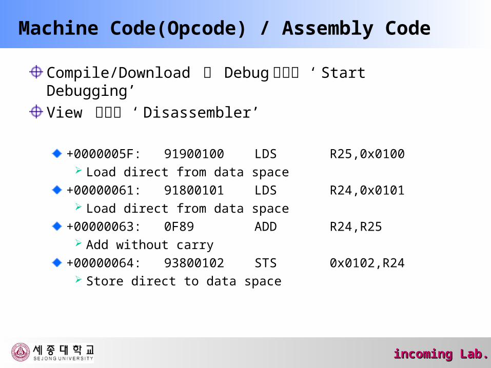
Machine Code(Opcode) / Assembly Code
Compile/Download 후 Debug 메뉴의 ‘ Start Debugging’View 메뉴의 ‘ Disassembler’
+0000005F: 91900100 LDS R25,0x0100 Load direct from data space
+00000061: 91800101 LDS R24,0x0101 Load direct from data space
+00000063: 0F89 ADD R24,R25 Add without carry
+00000064: 93800102 STS 0x0102,R24 Store direct to data space

incoming Lab.incoming Lab.
Instruction Example :
int main(){
unsigned int *a,*b,*c;
a = (unsigned int *)0x100; b = (unsigned int *)0x101; c = (unsigned int *)0x102;
*c = *a + *b;
return 0;}

incoming Lab.incoming Lab.
Machine Code(Opcode) / Assembly Code
Program address
Opcode Assembly Code

incoming Lab.incoming Lab.
Instruction Example :
int main(){
unsigned int *a,*b,*c;
a = (unsigned int *)0x100; b = (unsigned int *)0x102; c = (unsigned int *)0x104;
return 0;}

incoming Lab.incoming Lab.
Machine Code(Opcode) / Assembly Code
Program address
Opcode Assembly Code

incoming Lab.incoming Lab.
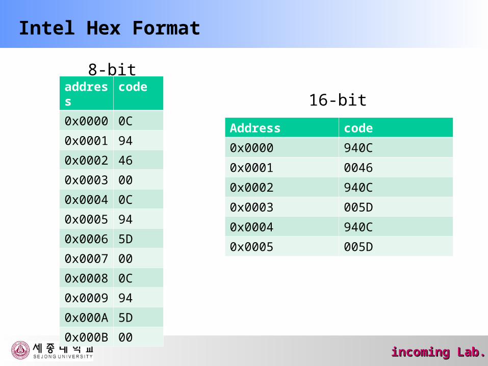
HEX File
Compile 결과물의 하나Project directory 아래 “ default” 폴더Intel Hex Format
:100000000C9446000C945D000C945D000C945D0013:100010000C945D000C945D000C945D000C945D00EC:100020000C945D000C945D000C945D000C945D00DC:100030000C945D000C945D000C945D000C945D00CC:100040000C945D000C945D000C945D000C945D00BC:100050000C945D000C945D000C945D000C945D00AC:100060000C945D000C945D000C945D000C945D009C:100070000C945D000C945D000C945D000C945D008C:100080000C945D000C945D000C945D0011241FBE67…

incoming Lab.incoming Lab.
Intel Hex Format
:100000000C9446000C945D000C945D000C945D0013
: 10 0000 00 0C 94 46 00 0C 94 5D 00 0C 94 5D 00 0C 94 5D 00 13
incoming Lab.incoming Lab.
Intel Hex Format
address
code
0x0000
0C
0x0001
94
0x0002
46
0x0003
00
0x0004
0C
0x0005
94
0x0006
5D
0x0007
00
0x0008
0C
0x0009
94
0x000A
5D
0x000B
00
Address code
0x0000 940C
0x0001 0046
0x0002 940C
0x0003 005D
0x0004 940C
0x0005 005D
16-bit
8-bit


![[창업에듀]02. 아이템 성공하는 비즈니스모델 구축전략](https://static.fdocument.pub/doc/165x107/58ed34c61a28ab2d588b46b5/02-58ed34c61a28ab2d588b46b5.jpg)