wf1907sch
34
Published by LITE-ON Service Printed in Taiwan All rights reserved Subject to modification 31th Oct-2006 © Any person attempting to service this chassis must familarize with the chassis and be aware of the necessary safety precautions to be used when serving electronic equipment containing high voltage. Service Manual Service HP HP 1907 & W1907 WF HP_LCD_W1907&WF1907_SM061031V00 Table of Contents 01. ----------------------------------------------------------------01 02. --------------------------------------------------------------------------------------02 03. --------------------------------------------------------------------------------03 04. ------------------------------------------------------------------------------------10 05. -------------------------------------------------------------------------------------------24 Power Board Operation Theory Inverter Circuit Interface Operation Troubleshooting Schematic Safety Notice
-
Upload
alana-clark -
Category
Documents
-
view
2 -
download
0
Transcript of wf1907sch
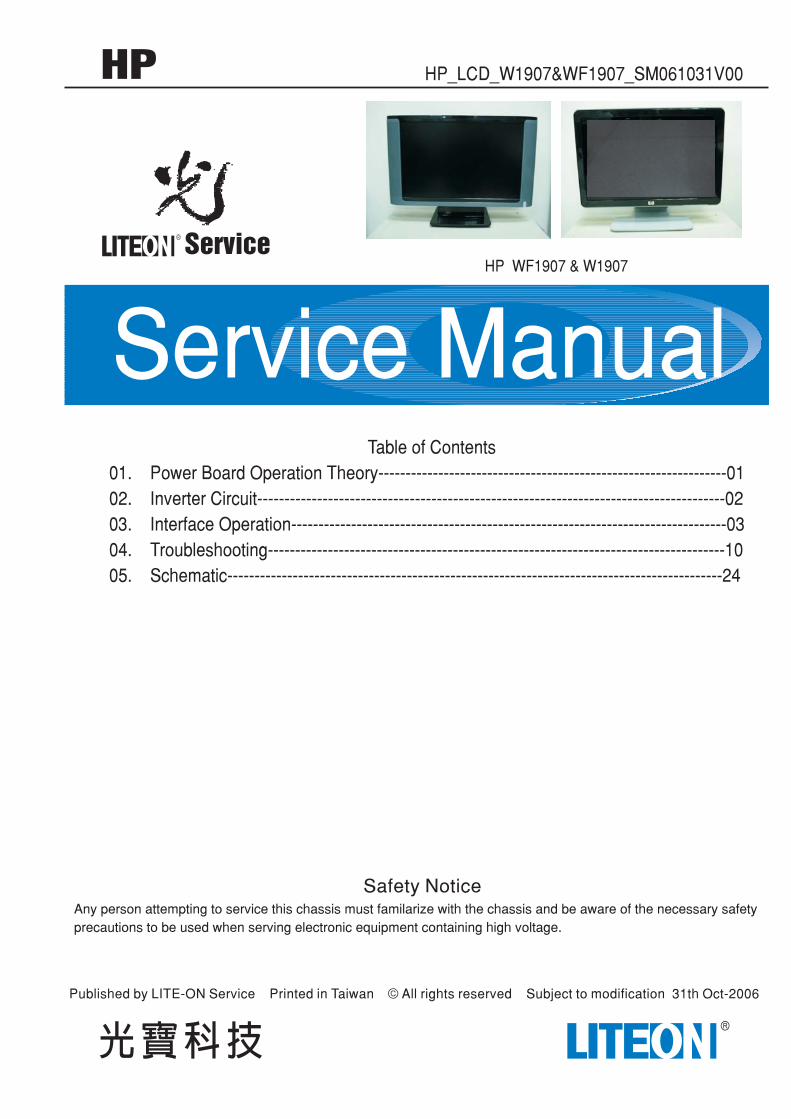
Published by LITE-ON Service Printed in Taiwan All rights reserved Subject to modification 31th Oct-2006©
Any person attempting to service this chassis must familarize with the chassis and be aware of the necessary safety
precautions to be used when serving electronic equipment containing high voltage.
June.19th-2006
Service Manual
Service
HP
HP 1907 & W1907WF
HP_LCD_W1907&WF1907_SM061031V00
Table of Contents
01. ----------------------------------------------------------------01
02. --------------------------------------------------------------------------------------02
03. --------------------------------------------------------------------------------03
04. ------------------------------------------------------------------------------------10
05. -------------------------------------------------------------------------------------------24
Power Board Operation Theory
Inverter Circuit
Interface Operation
Troubleshooting
Schematic
Safety Notice
Page 1
HP W1907& WF1907 Service Manual
1. Power Board Operation Theory 1.1 Line filter consists of C801, T801, C802, C803, C804, C808, C809, C815, C819, C820, C825. It eliminates high frequency interference to meet EMI’s requirement. 1.2 Rec & Filter Bridge diode D812, D813, D814, D815 converts AC source into pulsed DC. This pulsed DC is smoothed and filtered by C805. R802 is an NTC (negative thermal coefficient ) resistor, used to reduce inrush current to be within safe range. 1.3 Power transformer : T802 converts energy for square wave from power source C805 to secondary side to generate +5V, +12V and +22V. 1.4 Output : The square wave from T802 is rectified by D808 D809, D810, then filtered by C817, C818, C824, C823, C830, C833, C822 to generate +22.5V and +12V, +5V respectively. 1.5 Driver : Q803 drive T802 from PWM control of I801 for power converted. 1.6 FB : Negative feedback CKT consists of photo coupler I802 and adjustable regulator I803. It can maintain output voltages +22.5V and +12V, +5V at a stable level. 1.7 PWM :
1.7.1 Start : When power is turned on. C807 is charged a 11V and a starting current above 40uA to pin 1 of I801. I801 starts to oscillate and outputs a pulse train through pin 6 to drive Q803.
1.7.2 OPP : When Q803 turns on, C805 supplies a linearly increasing triangle current through the primary inductance of T802 to the driver Q803, once the peak value of this current multiplied by R811 exceeds 0.52V, pulse train will be turn off immediately to protect Q803, T802 from being burned out.
1.7.3 Regulation : If output voltage +22V goes up, the R terminal of I803 gets more bias, accordingly photo transistor and photo diode flows more current. The voltage of pin 2 goes up too, making the pulse width of pin 6 to become narrower. So the output voltage +22V will be pulled down to a stable value.
1.7.4 OVP : If +22.5V goes up too much, the induced voltage on pin 4 of T802 becomes large also. Suppose that it is over 20V. The pulse train at pin 6 goes down to zero, shutting Q803 off immediately.
1.7.5 SCP : If output terminal is short to ground, photo transistor does not conduct, hence I802 does not conduct either. Then oscillation of I801 is stop, shutting Q803 off immediately.
Page 2
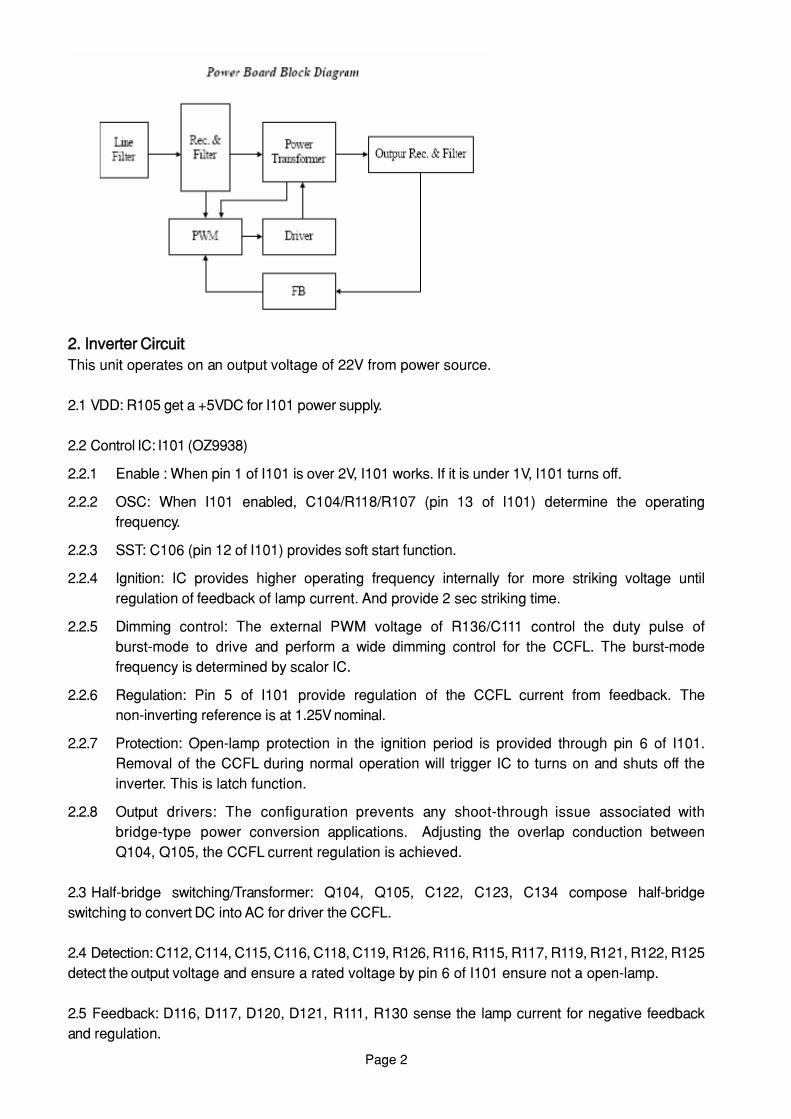
2. Inverter Circuit This unit operates on an output voltage of 22V from power source. 2.1 VDD: R105 get a +5VDC for I101 power supply. 2.2 Control IC: I101 (OZ9938)
2.2.1 Enable : When pin 1 of I101 is over 2V, I101 works. If it is under 1V, I101 turns off.
2.2.2 OSC: When I101 enabled, C104/R118/R107 (pin 13 of I101) determine the operating frequency.
2.2.3 SST: C106 (pin 12 of I101) provides soft start function.
2.2.4 Ignition: IC provides higher operating frequency internally for more striking voltage until regulation of feedback of lamp current. And provide 2 sec striking time.
2.2.5 Dimming control: The external PWM voltage of R136/C111 control the duty pulse of burst-mode to drive and perform a wide dimming control for the CCFL. The burst-mode frequency is determined by scalor IC.
2.2.6 Regulation: Pin 5 of I101 provide regulation of the CCFL current from feedback. The non-inverting reference is at 1.25V nominal.
2.2.7 Protection: Open-lamp protection in the ignition period is provided through pin 6 of I101. Removal of the CCFL during normal operation will trigger IC to turns on and shuts off the inverter. This is latch function.
2.2.8 Output drivers: The configuration prevents any shoot-through issue associated with bridge-type power conversion applications. Adjusting the overlap conduction between Q104, Q105, the CCFL current regulation is achieved.
2.3 Half-bridge switching/Transformer: Q104, Q105, C122, C123, C134 compose half-bridge switching to convert DC into AC for driver the CCFL. 2.4 Detection: C112, C114, C115, C116, C118, C119, R126, R116, R115, R117, R119, R121, R122, R125 detect the output voltage and ensure a rated voltage by pin 6 of I101 ensure not a open-lamp. 2.5 Feedback: D116, D117, D120, D121, R111, R130 sense the lamp current for negative feedback and regulation.
Page 3
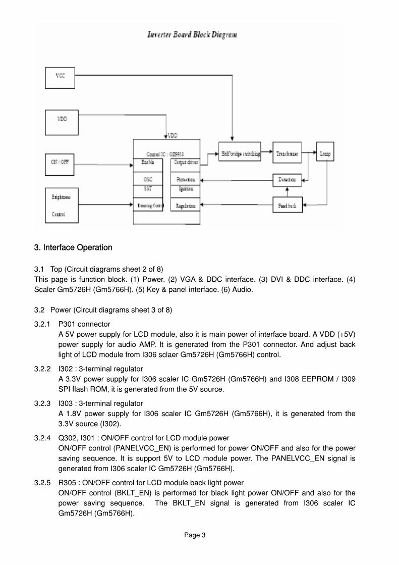
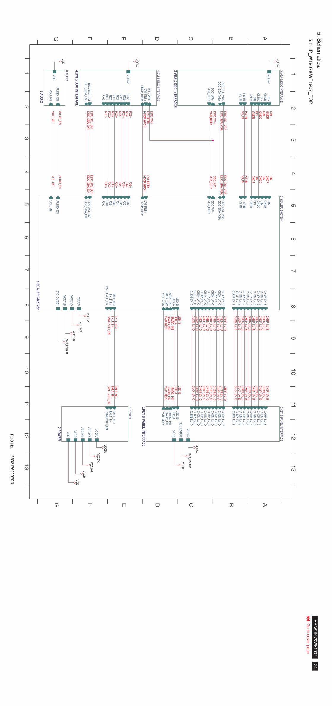
3. Interface Operation 3.1 Top (Circuit diagrams sheet 2 of 8) This page is function block. (1) Power. (2) VGA & DDC interface. (3) DVI & DDC interface. (4) Scaler Gm5726H (Gm5766H). (5) Key & panel interface. (6) Audio. 3.2 Power (Circuit diagrams sheet 3 of 8)
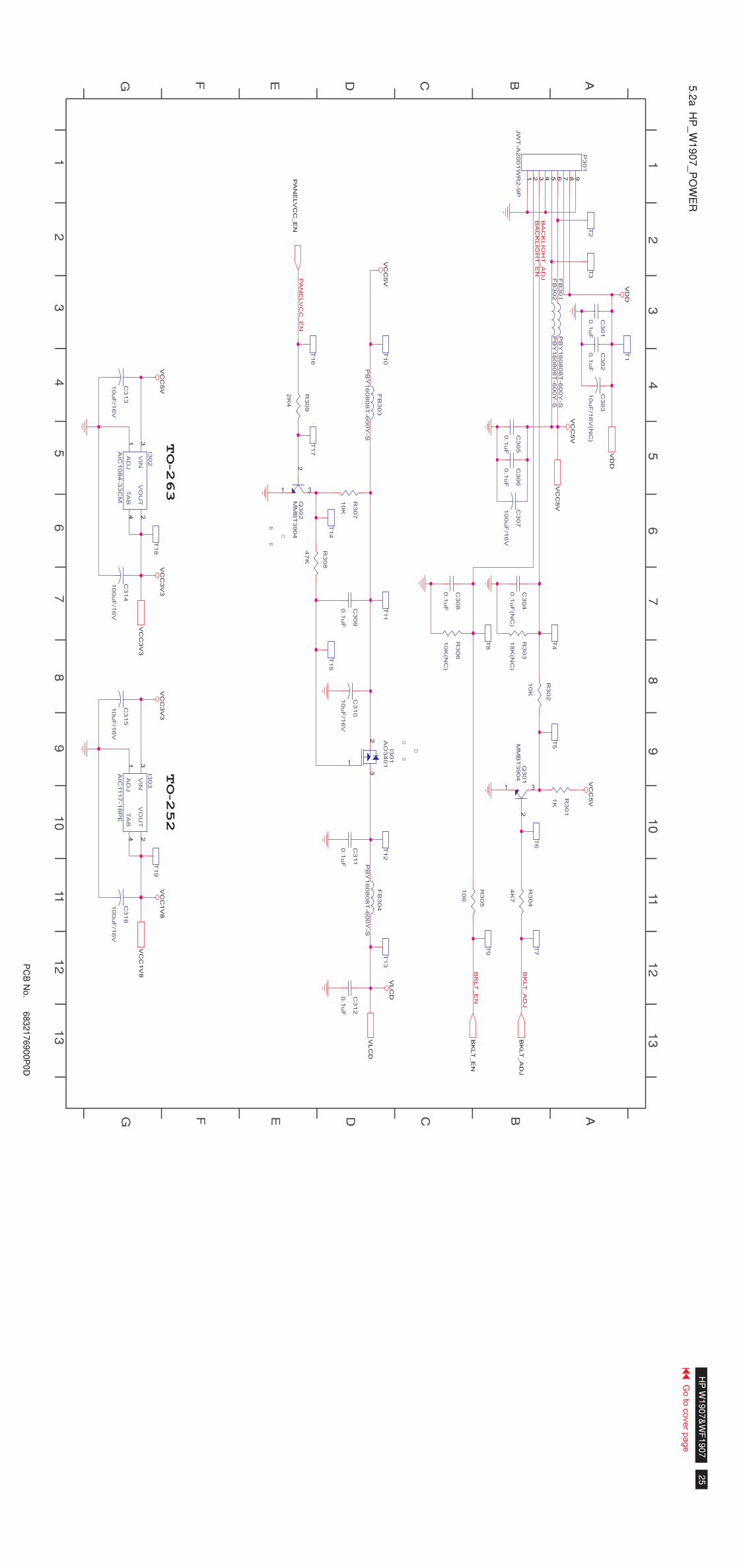
3.2.1 P301 connector A 5V power supply for LCD module, also it is main power of interface board. A VDD (+5V) power supply for audio AMP. It is generated from the P301 connector. And adjust back light of LCD module from I306 sclaer Gm5726H (Gm5766H) control.
3.2.2 I302 : 3-terminal regulator A 3.3V power supply for I306 scaler IC Gm5726H (Gm5766H) and I308 EEPROM / I309 SPI flash ROM, it is generated from the 5V source.
3.2.3 I303 : 3-terminal regulator A 1.8V power supply for I306 scaler IC Gm5726H (Gm5766H), it is generated from the 3.3V source (I302).
3.2.4 Q302, I301 : ON/OFF control for LCD module power ON/OFF control (PANELVCC_EN) is performed for power ON/OFF and also for the power saving sequence. It is support 5V to LCD module power. The PANELVCC_EN signal is generated from I306 scaler IC Gm5726H (Gm5766H).
3.2.5 R305 : ON/OFF control for LCD module back light power ON/OFF control (BKLT_EN) is performed for black light power ON/OFF and also for the power saving sequence. The BKLT_EN signal is generated from I306 scaler IC Gm5726H (Gm5766H).
Page 4
3.2.6 Q301, R301, R302, R304 : Adjust back light luminance of LCD module It is adjusted back light luminance control (BKLT_ADJ) is performed for the back light luminance. The BKLT_ADJ signal is generated from I306 scaler IC Gm5726H (Gm5766H).
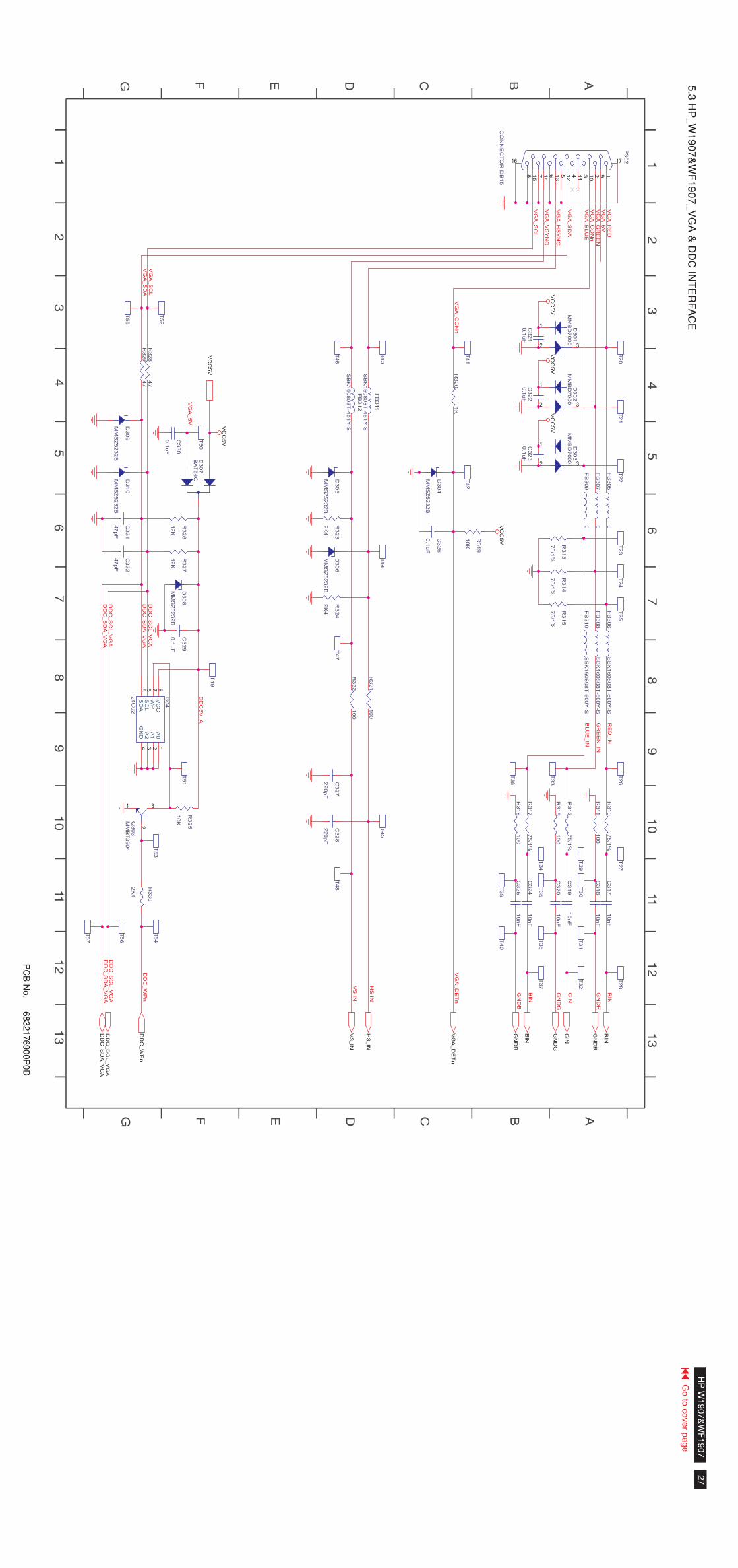
3.3 VGA & DDC interface (Circuit diagrams sheet 4 of 8) This sheet has RGB analog video and H/V sync signals input from VGA connector. The RGB analog video signals input through AC-coupled, analog video signal is used to clamp the black level at 0V. And H/V sync to sclaer. Support EDID plug & play function for analog video. It is to support VESA DDC/CI interface for analog video.
3.3.1 P302 connector The RGB analog video and H/V sync input signals to I306 scaler Gm5726H (Gm5766H). The VESA DDC/CI function is through I2C bus to I306 scaler Gm5726H (Gm5766H).
3.3.2 I304 : EDID EEPROM (24LC02B) The I304 is support EDID information of the VESA standard for VGA interface, and support plug and play for the PC host.
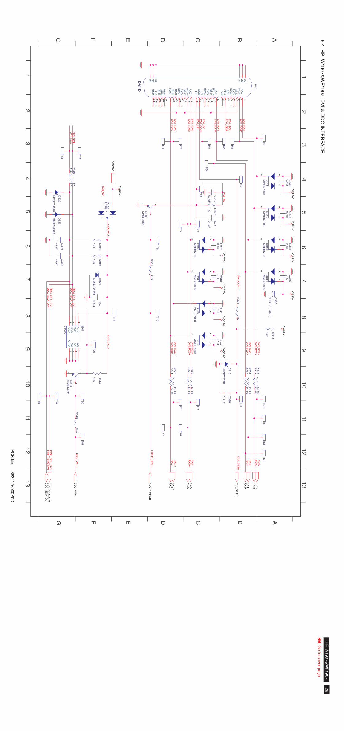
3.4 DVI & DDC interface (Circuit diagrams sheet 5 of 8) The digital video signals (TMDS) input from P303 DVI-D connector. The digital video signal is TMDS for DVI V1.0 standard. And support EDID plug & play function for digital video. It is to support VESA DDC/CI interface, and support HDCP function.
3.4.1 P303 connector P303 is DVI-D connector for DDWG standard, it have digital video signals (TMDS) to I306 scaler Gm5726H (Gm5766H). The VESA DDC/CI function is through I2C bus to I306 Gm5726H (Gm5766H). And support HDCP function is also through I2C bus to I306 Gm5726H (Gm5766H).
3.4.2 I305 : EDID EEPROM (24LC02B) The I305 is support EDID information of the VESA standard for DVI interface, and support plug and play for the PC host.
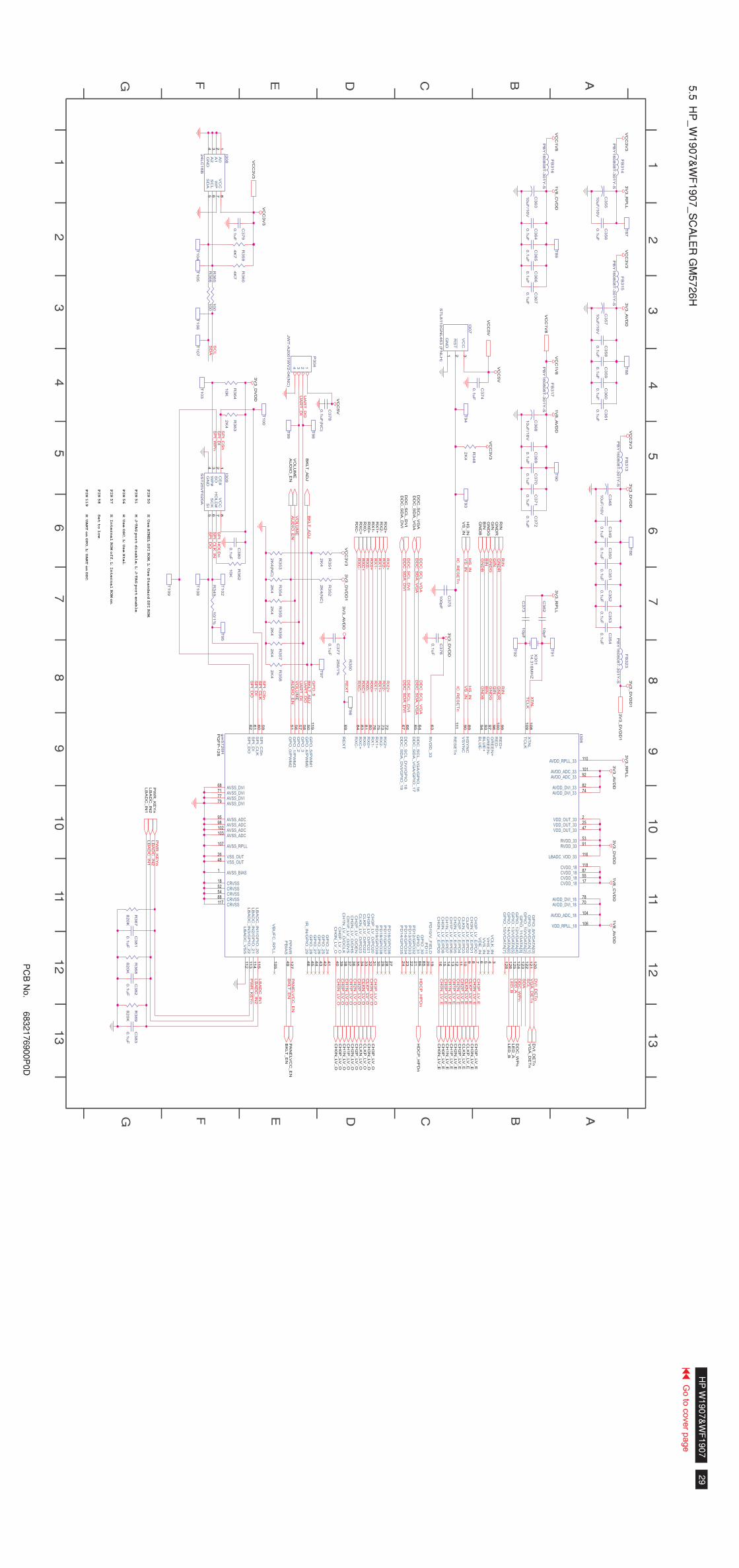
3.5 Scaler Gm5726H (Gm5766H) (Circuit diagrams sheet 6 of 8) The I306 Gm5726H (Gm5766H) is all-in-one LCD monitor controller. The Gm5726H (Gm5766H) leverages Genesis patented advanced image-processing technology as well as a proven integrated ADC/PLL and an Ultra-Reliable DVI compliant receiver to provide excellent image quality. Gm5726H (Gm5766H) also integrates HDCP function, a micro-controller, an OSD controller, and dual LVDS. The RGB analog video signal from video input circuit enter to incorporated A/D converted block (ADC) into the digital data for analog video signal. The TMDS digital signals input (with HDCP) entered from the DVI-D connector is converted into the digital data. Based on this conversion, this device performs interpolation during pixel extension. These interpolation digital data are transformed to LVDS signal. The I306 source voltage is 3.3V and 1.8V, the device clock source frequency is 14.318 MHz. And support DDC/CI interface of VESA and function key operation.
Page 5
3.5.1 I308 EEPROM (24LC16B)
The control data and parameter, and OSD related setting, and other service data, to be stored in I308. The contents of which are updated as required.
3.5.2 I309 SPI Flash ROM The firmware program running from I309 external SPI flash ROM, contains firmware code and data for all firmware function. The device is 2Mbits of flash ROM.
3.5.3 I307 Microprocessor Supervisory Circuit The function of this device is to assert a reset to I306 scaler Gm5726H (Gm5766H), when either the power supply dropped down.
3.5.4 X301 14.318MHz It generated reference clock input for I306 scaler.
3.5.5 ISP and DDC/CI function The DDC/CI is VESA standard for the host PC system, it can through I2C bus to control LCD monitor. Enter I306 pin64 DDC_SCL_A and pin65 DDC_SDA_A of the VGA port. Enter I306 pin66 DDC_SCL_D pin67 DDC_SDA_D of the DVI-D port. It use ISP function when change new firmware to I309 SPI flash ROM, it used I2C bus from VGA or DVI-D port through I306 Gm5726H (Gm5766H) to I309 SPI flash ROM.
3.5.6 The power save sequence function First I306 pin49 (BKLT_EN) set Low to disable LCD module back light power, delay of some time, then I306 pin127 (PANELVCC_EN) set Low to disable LCD module power, then I306 enter to power down mode.
3.6 Key & Panel interface (Circuit diagrams sheet 7of 8)
3.6.1 P306 connector It is LVDS bus, it is from I306 scaler to LCD panel module. The P306 output voltage is 5V.
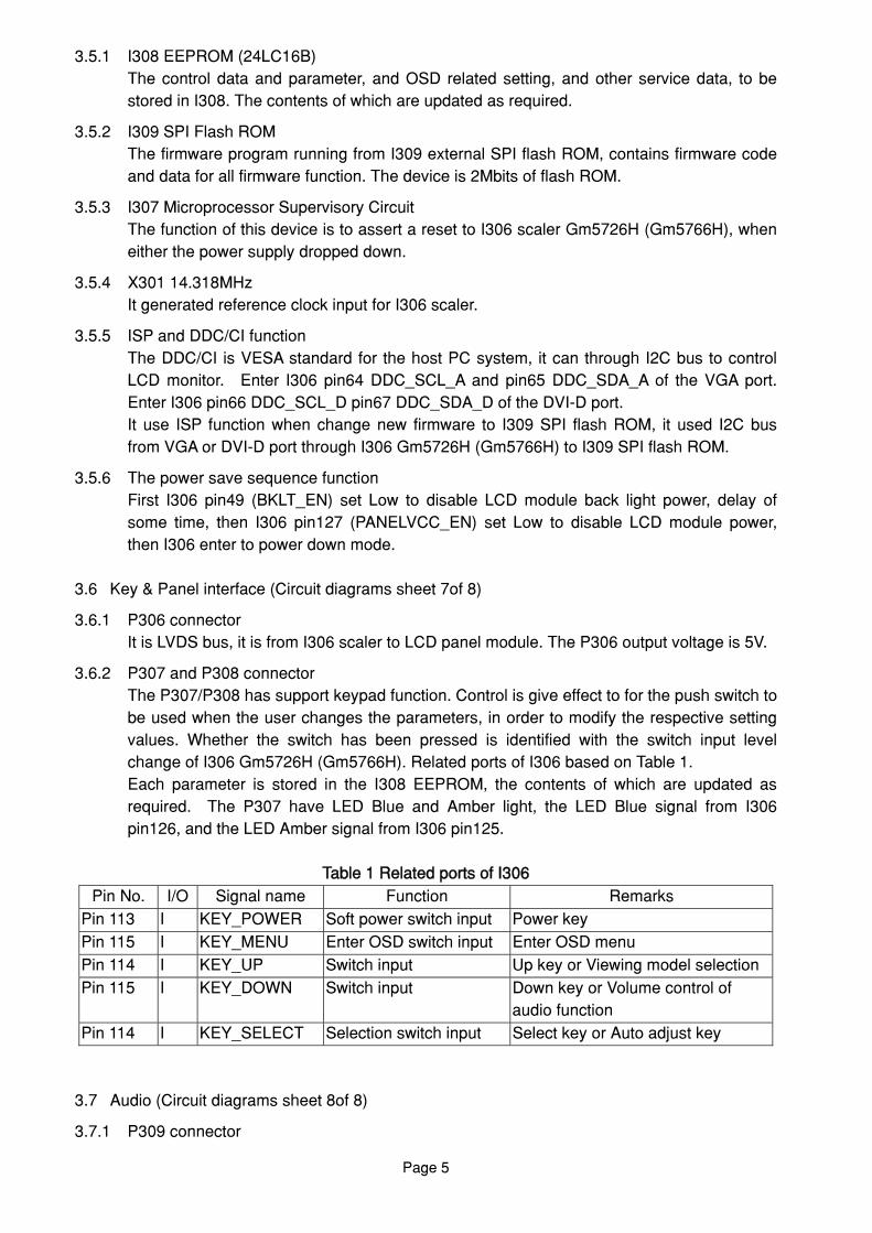
3.6.2 P307 and P308 connector The P307/P308 has support keypad function. Control is give effect to for the push switch to be used when the user changes the parameters, in order to modify the respective setting values. Whether the switch has been pressed is identified with the switch input level change of I306 Gm5726H (Gm5766H). Related ports of I306 based on Table 1. Each parameter is stored in the I308 EEPROM, the contents of which are updated as required. The P307 have LED Blue and Amber light, the LED Blue signal from I306 pin126, and the LED Amber signal from I306 pin125.
Table 1 Related ports of I306
Pin No. I/O Signal name Function Remarks Pin 113 I KEY_POWER Soft power switch input Power key Pin 115 I KEY_MENU Enter OSD switch input Enter OSD menu Pin 114 I KEY_UP Switch input Up key or Viewing model selection Pin 115 I KEY_DOWN Switch input Down key or Volume control of
audio function Pin 114 I KEY_SELECT Selection switch input Select key or Auto adjust key
3.7 Audio (Circuit diagrams sheet 8of 8)
3.7.1 P309 connector

Page 6
The P309 is audio signal input from the audio source.
3.7.2 P310 connector The P310 is audio output to speaker and support 2W x 2 speakers.
3.7.3 I310 TPA6021A4 The I310 is 2x2W stereo audio amplifier, it is an integrated class-AB dual output amplifier.
3.7.4 Q309 : Power down and mute control for Audio ON/OFF control (AUDIO_EN) is performed for standby mode and mute function. It is support 5V to audio IC power. The AUDIO_EN signal is generated from I306 scaler Gm5726H (Gm5766H).
3.7.5 R394, Q310: Volume control for Audio Volume control (volume) is performed for audio output signal power. The volume signal is generated from I306 scaler Gm5726H (Gm5766H).
3.8 Others
3.8.1 Detection of POWER ON status The I306 Gm5726H (Gm5766H) identified the ON status of two modes for the power supplies. The identification is made when the power supply is turn off. For example, if the power supply is turn off with the POWER key switch, the POWER key switch must be turn on when active the power supply again. If the power supply turned off by the pulling out the power cord, then this power supply can to be turned on by connecting the power cord, without pressing the POWER key switch.
3.8.2 Display mode identification
3.8.2.1 Display mode identification The display mode of input signal is identified based on Table 2. When the mode has been identified through the measurement of horizontal
and vertical frequencies, the total number of lines is determined with a formula of “Horizontal frequency / Vertical frequency = Total number of number of lines”. Final identification can be made by examining the coincidence of the obtained figure with the number of lines for the mode identified from the frequency. The Distinction Hsync and Vsync of each mode is shown in Table 3.
When the detected frequency if the sync signal has changed, the total number of lines should be counted even through it is range identified frequency in the same mode.
3.8.2.2 Out of range This out of range mode is assumed when the frequency out of the horizontal / vertical signal is as specified below.
Vertical frequency : 50 ~ 76 Hz. Horizontal frequency : 24 ~ 83KHz.
3.8.2.3 Power save mode
The power save mode is assumed when the horizontal / vertical signals are as specified below.
If there is no horizontal sync signal input. If there is no vertical sync signal input. If the horizontal sync signal is outside the measuring range of I306 Gm5726H
(Gm5766H). If the vertical sync signal is outside the measuring range of I306 Gm5726H
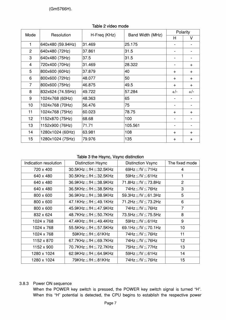
Page 7
(Gm5766H).
Table 2 video mode
Polarity Mode Resolution H-Freq (KHz) Band Width (MHz)
H V
1 640x480 (59.94Hz) 31.469 25.175 - - 2 640x480 (72Hz) 37.861 31.5 - - 3 640x480 (75Hz) 37.5 31.5 - - 4 720x400 (70Hz) 31.469 28.322 - + 5 800x600 (60Hz) 37.879 40 + + 6 800x600 (72Hz) 48.077 50 + + 7 800x600 (75Hz) 46.875 49.5 + + 8 832x624 (74.55Hz) 49.722 57.284 +/- +/- 9 1024x768 (60Hz) 48.363 65 - -
10 1024x768 (70Hz) 56.476 75 - - 11 1024x768 (75Hz) 60.023 78.75 + + 12 1152x870 (75Hz) 68.68 100 - - 13 1152x900 (76Hz) 71.71 105.561 - - 14 1280x1024 (60Hz) 63.981 108 + + 15 1280x1024 (75Hz) 79.976 135 + +
Table 3 the Hsync, Vsync distinction
Indication resolution Distinction Hsync Distinction Vsync The fixed mode
720 x 400 30.5KHz≦fH≦32.5KHz 69Hz≦fV≦71Hz 4
640 x 480 30.5KHz≦fH≦32.5KHz 59Hz≦fV≦61Hz 1
640 x 480 36.9KHz≦fH≦38.9KHz 71.8Hz≦fV≦73.8Hz 2
640 x 480 36.5KHz≦fH≦38.5KHz 74Hz≦fV≦76Hz 3
800 x 600 36.9KHz≦fH≦38.9KHz 59.3Hz≦fV≦61.3Hz 5
800 x 600 47.1KHz≦fH≦49.1KHz 71.2Hz≦fV≦73.2Hz 6
800 x 600 45.9KHz≦fH≦47.9KHz 74Hz≦fV≦76Hz 7
832 x 624 48.7KHz≦fH≦50.7KHz 73.5Hz≦fV≦75.5Hz 8
1024 x 768 47.4KHz≦fH≦49.4KHz 59Hz≦fV≦61Hz 9
1024 x 768 55.5KHz≦fH≦57.5KHz 69.1Hz≦fV≦70.1Hz 10
1024 x 768 59KHz≦fH≦61KHz 74Hz≦fV 76Hz≦ 11
1152 x 870 67.7KHz fH 69.7KHz≦ ≦ 74Hz fV 76Hz≦ ≦ 12
1152 x 900 70.7KHz fH 72.7KHz≦ ≦ 75Hz fV 77Hz≦ ≦ 13
1280 x 1024 62.9KHz fH 64.9KHz≦ ≦ 59Hz fV 61Hz≦ ≦ 14
1280 x 1024 79KHz fH 81KHz≦ ≦ 74Hz fV 76Hz≦ ≦ 15
3.8.3 Power ON sequence
When the POWER key switch is pressed, the POWER key switch signal is turned “H”. When this “H” potential is detected, the CPU begins to establish the respective power
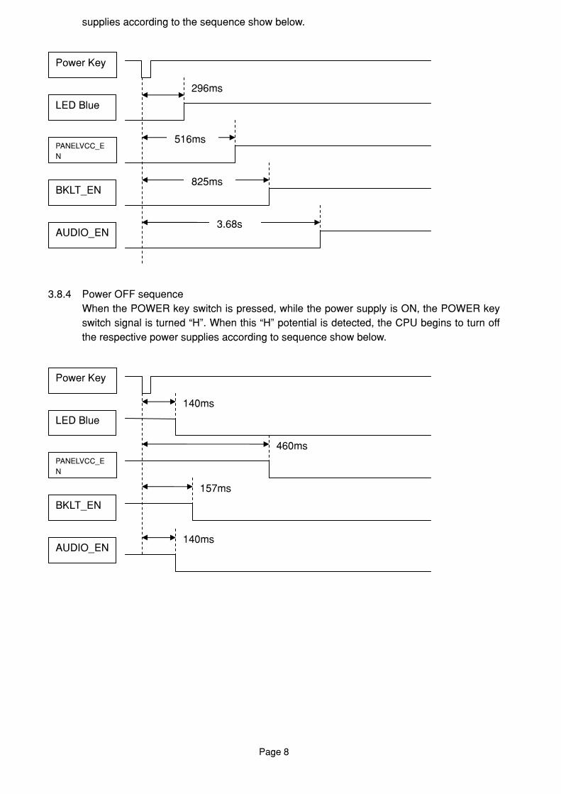
Page 8
supplies according to the sequence show below.
3.8.4 Power OFF sequence
When the POWER key switch is pressed, while the power supply is ON, the POWER key switch signal is turned “H”. When this “H” potential is detected, the CPU begins to turn off the respective power supplies according to sequence show below.
460ms
157ms
140ms
140ms
Power Key
LED Blue
PANELVCC_EN
BKLT_EN
AUDIO_EN
296ms
Power Key
LED Blue
PANELVCC_EN
BKLT_EN
AUDIO_EN
516ms
825ms
3.68s
Page 9
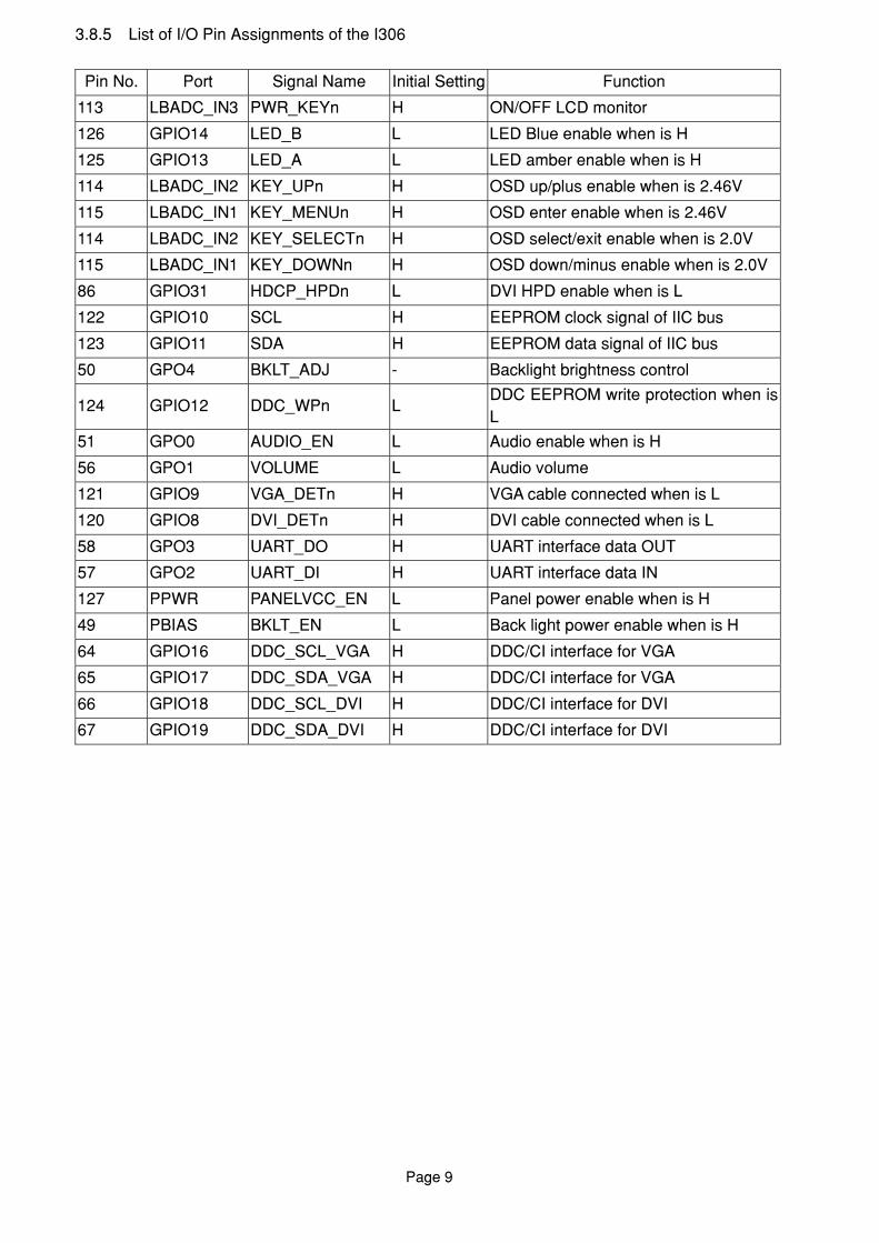
3.8.5 List of I/O Pin Assignments of the I306
Pin No. Port Signal Name Initial Setting Function
113 LBADC_IN3 PWR_KEYn H ON/OFF LCD monitor
126 GPIO14 LED_B L LED Blue enable when is H
125 GPIO13 LED_A L LED amber enable when is H
114 LBADC_IN2 KEY_UPn H OSD up/plus enable when is 2.46V
115 LBADC_IN1 KEY_MENUn H OSD enter enable when is 2.46V
114 LBADC_IN2 KEY_SELECTn H OSD select/exit enable when is 2.0V
115 LBADC_IN1 KEY_DOWNn H OSD down/minus enable when is 2.0V
86 GPIO31 HDCP_HPDn L DVI HPD enable when is L
122 GPIO10 SCL H EEPROM clock signal of IIC bus
123 GPIO11 SDA H EEPROM data signal of IIC bus
50 GPO4 BKLT_ADJ - Backlight brightness control
124 GPIO12 DDC_WPn L DDC EEPROM write protection when is L
51 GPO0 AUDIO_EN L Audio enable when is H
56 GPO1 VOLUME L Audio volume
121 GPIO9 VGA_DETn H VGA cable connected when is L
120 GPIO8 DVI_DETn H DVI cable connected when is L
58 GPO3 UART_DO H UART interface data OUT
57 GPO2 UART_DI H UART interface data IN
127 PPWR PANELVCC_EN L Panel power enable when is H
49 PBIAS BKLT_EN L Back light power enable when is H
64 GPIO16 DDC_SCL_VGA H DDC/CI interface for VGA
65 GPIO17 DDC_SDA_VGA H DDC/CI interface for VGA
66 GPIO18 DDC_SCL_DVI H DDC/CI interface for DVI
67 GPIO19 DDC_SDA_DVI H DDC/CI interface for DVI

4. Troubleshooting
Does OSD display when you push MENU
button.
Yes
No Proceed "No OSD display" section.
Check if the sync signal from computer is
output and if the video cable is connected
normally. (VGA or DVI)
OK
Proceed "checking the resolution change IC
movement" section.
NGInput the sync signal of computer, or change
the cable. (VGA or DVI)
When a signal isn't being input, it is
indicated with "VIDEO INPUT". it is
indicated with "OUT OF RANGE" at the
time of the frequency that it can't be
distinguished.
Page 10
4.1 No.display of screen (Screen is black, color of LED is amber)
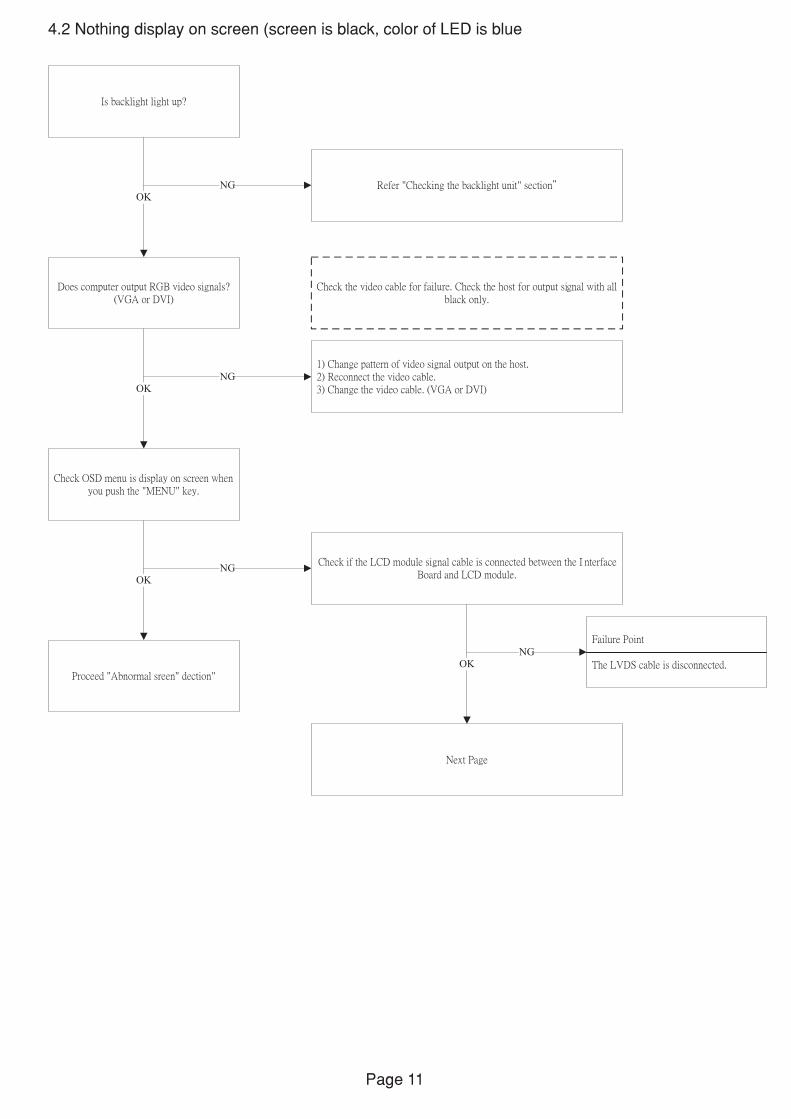
4.2 Nothing display on screen screen is black, color of LED is blue(
Is backlight light up?
Refer "Checking the backlight unit" section”OK
NG
Does computer output RGB video signals?
(VGA or DVI)
OK
Check OSD menu is display on screen when
you push the "MENU" key.
Proceed "Abnormal sreen" dection"
OK
NG
Check the video cable for failure. Check the host for output signal with all
black only.
1) Change pattern of video signal output on the host.
2) Reconnect the video cable.
3) Change the video cable. (VGA or DVI)
NGCheck if the LCD module signal cable is connected between the I nterface
Board and LCD module.
OK
Next Page
NG
Failure Point
The LVDS cable is disconnected.
Page 11
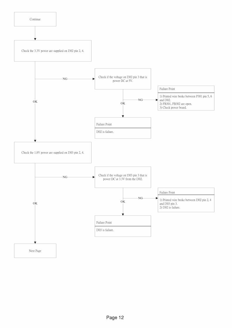
Continue
Check the 3.3V power are supplied on I302 pin 2, 4.
OK
NGCheck if the voltage on I302 pin 3 that is
power DC at 5V.
OK
Failure Point
I302 is failure.
NG
Failure Point
1) Printed wire broke between P301 pin 5, 6
and I302.
2) FB301, FB302 are open.
3) Check power board.
Check the 1.8V power are supplied on I303 pin 2, 4.
Check if the voltage on I303 pin 3 that is
power DC at 3.3V from the I302.
OK
Failure Point
I303 is failure.
NG
Failure Point
1) Printed wire broke between I302 pin 2, 4
and I303 pin 3.
2) I302 is failure.
OK
NG
Next Page
Page 12
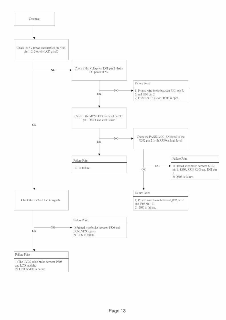
Check the 5V power are supplied on P306
pin 1, 2, 3 (to the LCD panel)
Continue
OK
NGCheck if the Voltage on I301 pin 2 that is
DC power at 5V.
OK
NG
Failure Point
1) Printed wire broke between P301 pin 5,
6, and I301 pin 2.
2) FB301 or FB302 or FB303 is open.
Check if the MOS FET Gate level on I301
pin 1, that Gate level is low.
OK
NG
OK
NG
Failure Point
1) Printed wire broke between Q302
pin 3, R307, R308, C309 and I301 pin
1.
2) Q302 is failure.
Failure Point
1) Printed wire broke between Q302 pin 2
and I306 pin 127.
2) I306 is failure.
Check the PANELVCC_EN signal of the
Q302 pin 2 (with R309) at high level.
Failure Point
I301 is failure.
Check the P306 all LVDS signals.
Failure Point
1) Printed wire broke between P306 and
I306 LVDS signals.
2) I306 is failure.
Failure Point
1) The LVDS cable broke between P306
and LCD module.
2) LCD module is failure.
OK
NG
Page 13
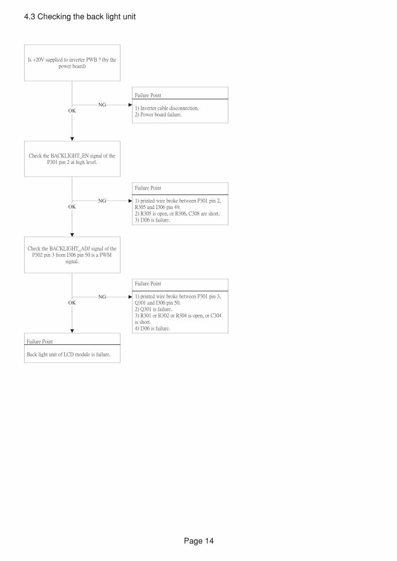
Is +20V supplied to inverter PWB ? (by the
power board)
4.3 Checking the back light unit
OK
NG
Failure Point
1) Inverter cable disconnection.
2) Power board failure.
Check the BACKLIGHT_EN signal of the
P301 pin 2 at high level.
OK
NG
Failure Point
1) printed wire broke between P301 pin 2,
R305 and I306 pin 49.
2) R305 is open, or R306, C308 are short.
3) I306 is failure.
Check the BACKLIGHT_ADJ signal of the
P302 pin 3 from I306 pin 50 is a PWM
signal.
OK
NG
Failure Point
1) printed wire broke between P301 pin 3,
Q301 and I306 pin 50.
2) Q301 is failure.
3) R301 or R302 or R304 is open, or C304
is short.
4) I306 is failure.
Failure Point
Back light unit of LCD module is failure.
Page 14
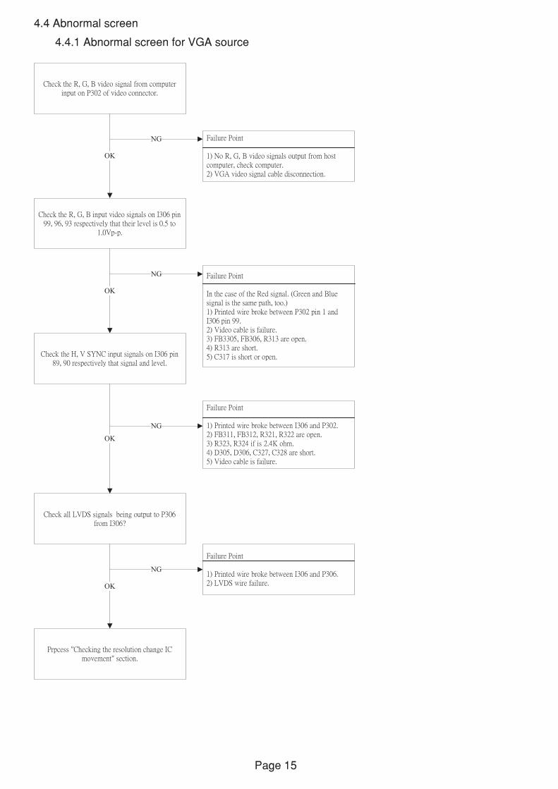
4.4 Abnormal screen
Check the R, G, B video signal from computer
input on P302 of video connector.
OK
NG Failure Point
1) No R, G, B video signals output from host
computer, check computer.
2) VGA video signal cable disconnection.
Check the R, G, B input video signals on I306 pin
99, 96, 93 respectively that their level is 0.5 to
1.0Vp-p.
Failure Point
In the case of the Red signal. (Green and Blue
signal is the same path, too.)
1) Printed wire broke between P302 pin 1 and
I306 pin 99.
2) Video cable is failure.
3) FB3305, FB306, R313 are open.
4) R313 are short.
5) C317 is short or open.
NG
OK
Check all LVDS signals being output to P306
from I306?
Failure Point
1) Printed wire broke between I306 and P306.
2) LVDS wire failure.
NG
OK
Prpcess "Checking the resolution change IC
movement" section.
4.4.1 Abnormal screen for VGA source
Page 15
Check the H, V SYNC input signals on I306 pin
89, 90 respectively that signal and level.
NG
OK
Failure Point
1) Printed wire broke between I306 and P302.
2) FB311, FB312, R321, R322 are open.
3) R323, R324 if is 2.4K ohm.
4) D305, D306, C327, C328 are short.
5) Video cable is failure.
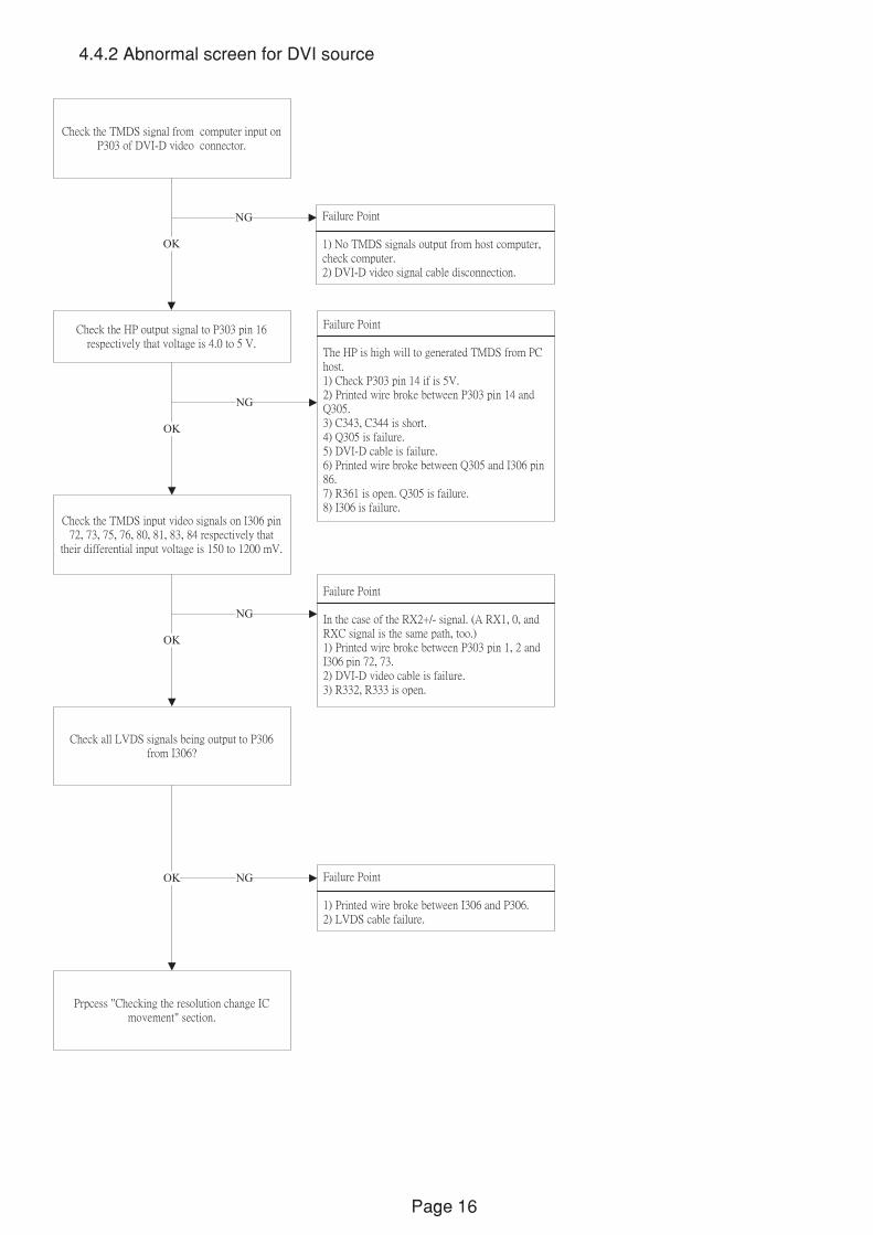
Check the TMDS signal from computer input on
P303 of DVI-D video connector.
OK
NG Failure Point
1) No TMDS signals output from host computer,
check computer.
2) DVI-D video signal cable disconnection.
Check the TMDS input video signals on I306 pin
72, 73, 75, 76, 80, 81, 83, 84 respectively that
their differential input voltage is 150 to 1200 mV.
Failure Point
In the case of the RX2+/- signal. (A RX1, 0, and
RXC signal is the same path, too.)
1) Printed wire broke between P303 pin 1, 2 and
I306 pin 72, 73.
2) DVI-D video cable is failure.
3) R332, R333 is open.
NG
OK
Check all LVDS signals being output to P306
from I306?
Failure Point
1) Printed wire broke between I306 and P306.
2) LVDS cable failure.
NGOK
Prpcess "Checking the resolution change IC
movement" section.
4.4.2 Abnormal screen for DVI source
Page 16
Check the HP output signal to P303 pin 16
respectively that voltage is 4.0 to 5 V.
NG
OK
Failure Point
The HP is high will to generated TMDS from PC
host.
1) Check P303 pin 14 if is 5V.
2) Printed wire broke between P303 pin 14 and
Q305.
3) C343, C344 is short.
4) Q305 is failure.
5) DVI-D cable is failure.
6) Printed wire broke between Q305 and I306 pin
86.
7) R361 is open. Q305 is failure.
8) I306 is failure.
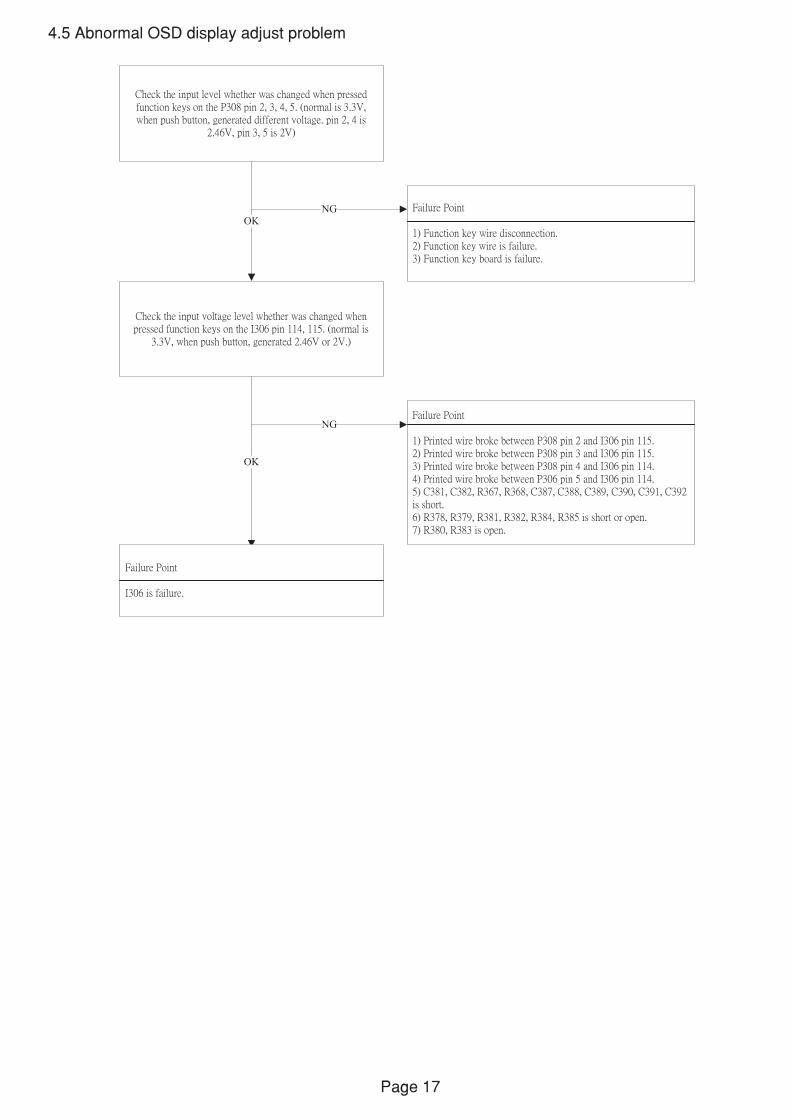
4.5 Abnormal OSD display adjust problem
Check the input level whether was changed when pressed
function keys on the P308 pin 2, 3, 4, 5. (normal is 3.3V,
when push button, generated different voltage. pin 2, 4 is
2.46V, pin 3, 5 is 2V)
OK
NG Failure Point
1) Function key wire disconnection.
2) Function key wire is failure.
3) Function key board is failure.
Check the input voltage level whether was changed when
pressed function keys on the I306 pin 114, 115. (normal is
3.3V, when push button, generated 2.46V or 2V.)
OK
NG
Failure Point
1) Printed wire broke between P308 pin 2 and I306 pin 115.
2) Printed wire broke between P308 pin 3 and I306 pin 115.
3) Printed wire broke between P308 pin 4 and I306 pin 114.
4) Printed wire broke between P306 pin 5 and I306 pin 114.
5) C381, C382, R367, R368, C387, C388, C389, C390, C391, C392
is short.
6) R378, R379, R381, R382, R384, R385 is short or open.
7) R380, R383 is open.
Failure Point
I306 is failure.
Page 17
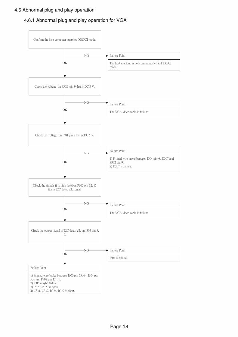
4.6 Abnormal plug and play operation
Confirm the host computer supplies DDC/CI mode.
OK
NG Failure Point
The host machine is not communicated in DDC/CI
mode.
Check the voltage on I304 pin 8 that is DC 5 V.
OK
NGFailure Point
1) Printed wire broke between I304 pinv8, D307 and
P302 pin 9.
2) D307 is failure.
Check the output signal of I2C data / clk on I304 pin 5,
6.
OK
NG Failure Point
I304 is failure.
Check the voltage on P302 pin 9 that is DC 5 V.
OK
NGFailure Point
The VGA video cable is failure.
Check the signals if is high level on P302 pin 12, 15
that is I2C data / clk signal.
OK
NGFailure Point
The VGA video cable is failure.
Failure Point
1) Printed wire broke between I306 pin 65, 64, I304 pin
5, 6 and P302 pin 12, 15.
2) I306 maybe failure.
3) R328, R329 is open.
4) C331, C332, R326, R327 is short.
4.6.1 Abnormal plug and play operation for VGA
Page 18
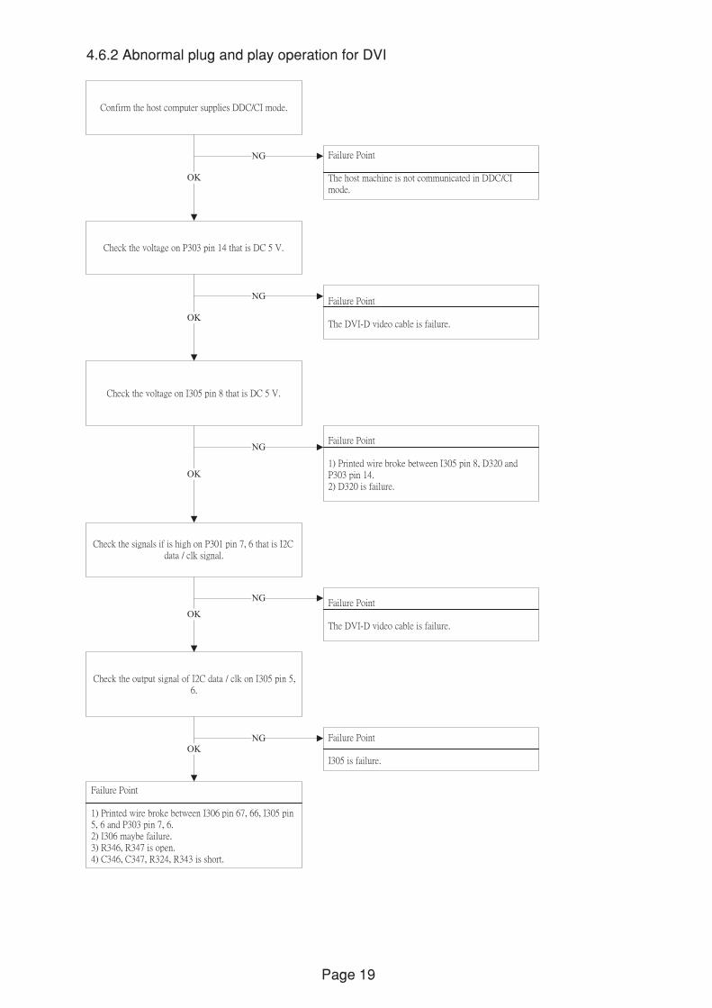
Confirm the host computer supplies DDC/CI mode.
OK
NG Failure Point
The host machine is not communicated in DDC/CI
mode.
Check the voltage on I305 pin 8 that is DC 5 V.
OK
NGFailure Point
1) Printed wire broke between I305 pin 8, D320 and
P303 pin 14.
2) D320 is failure.
Check the output signal of I2C data / clk on I305 pin 5,
6.
OK
NG Failure Point
I305 is failure.
Check the voltage on P303 pin 14 that is DC 5 V.
OK
NGFailure Point
The DVI-D video cable is failure.
Check the signals if is high on P301 pin 7, 6 that is I2C
data / clk signal.
OK
NGFailure Point
The DVI-D video cable is failure.
Failure Point
1) Printed wire broke between I306 pin 67, 66, I305 pin
5, 6 and P303 pin 7, 6.
2) I306 maybe failure.
3) R346, R347 is open.
4) C346, C347, R324, R343 is short.
4.6.2 Abnormal plug and play operation for DVI
Page 19
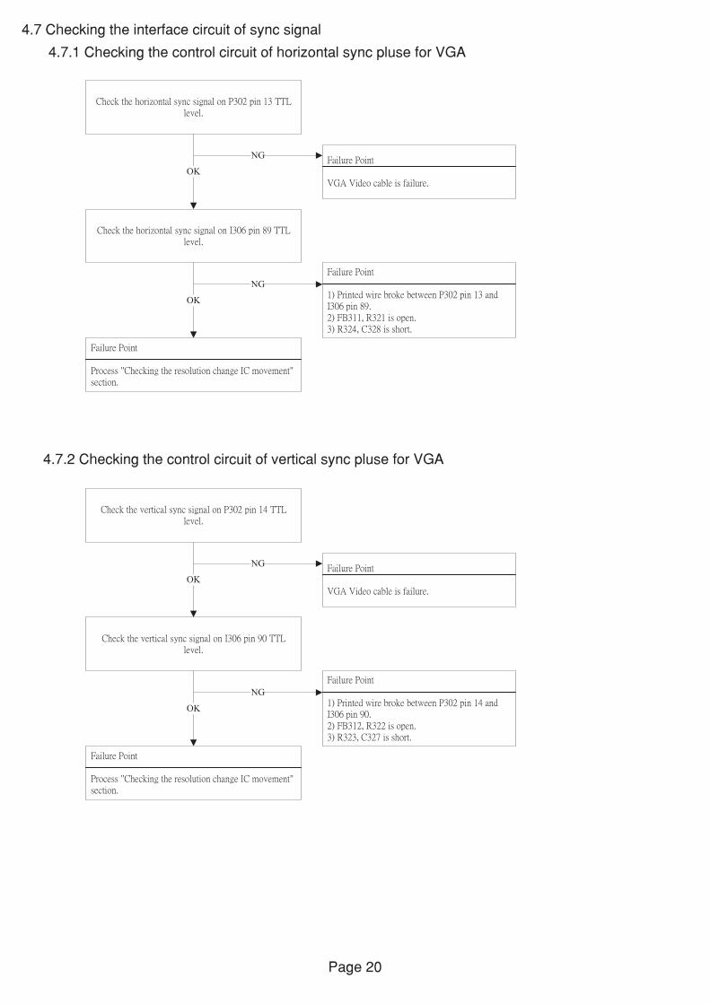
4.7 Checking the interface circuit of sync signal
4.7.1 Checking the control circuit of horizontal sync pluse for VGA
Check the horizontal sync signal on P302 pin 13 TTL
level.
OK
NGFailure Point
VGA Video cable is failure.
Check the horizontal sync signal on I306 pin 89 TTL
level.
OK
NG
Failure Point
1) Printed wire broke between P302 pin 13 and
I306 pin 89.
2) FB311, R321 is open.
3) R324, C328 is short.
Failure Point
Process "Checking the resolution change IC movement"
section.
4.7.2 Checking the control circuit of vertical sync pluse for VGA
Check the vertical sync signal on P302 pin 14 TTL
level.
OK
NGFailure Point
VGA Video cable is failure.
Check the vertical sync signal on I306 pin 90 TTL
level.
OK
NG
Failure Point
1) Printed wire broke between P302 pin 14 and
I306 pin 90.
2) FB312, R322 is open.
3) R323, C327 is short.
Failure Point
Process "Checking the resolution change IC movement"
section.
Page 20
4.8 Checking the resolution change IC movement
Check +3.3V supply on I306 pin 110, 101, 92, 82, 74, 2, 25,47, 53, 91,
116, 63.
OK
NG Proceed " Checking the DC/DC converter circuit" section.
Check +1.8V supply on I306 pin 118, 87, 55, 17, 78, 70, 104, 106.
OK
NG Proceed " Checking the DC/DC converter circuit" section.
Check X301 14.318MHz clock input to I306 pin 108 and 109.
OK
NGFailure Point
1) Printed wire broke between X301 and I306 pin 108, 109.
2) C362, C373 is short or open.
3) X301 failure.
Check I306 pin 111 RESETn signal is high level at normal operation.
OK
NG
Failure Point
1) Check I307 pin 2 is low level wait 200~250ms to high level, when
VCC5V is turned on.
2) I307 failure.
3) Printed wire broke between I306 pin 111 and I307.
4) C375 is short.
5) R348 is short or open.
6) I311 failure.
Check I306 pin 59~62 SPI ROM interface signal.
OK
NG
Failure Point
1) Printed wire broke between I306 pin 59~62 and I309.
2) I309 failure.
Failure Point
I311 failure.
Page 21
Check I306 pin 50, 51, 56~59, 119 Boot configure, when Reset signal
low to high.
OK
NG
Failure Point
1) Check I306 pin 50, if is low. R358 is open or short.
2) Check I306 pin 51, if is low. R354 is open or short.
3) Check I306 pin 56, if is low. R355 is open or short.
4) Check I306 pin 57, if is low. R356 is open or short.
5) Check I306 pin 58, if is low. R357 is open or short.
6) Check I306 pin 59, if is high. R363 is open or short.
7) Check I306 pin 119, if is high. R351 is open or short.
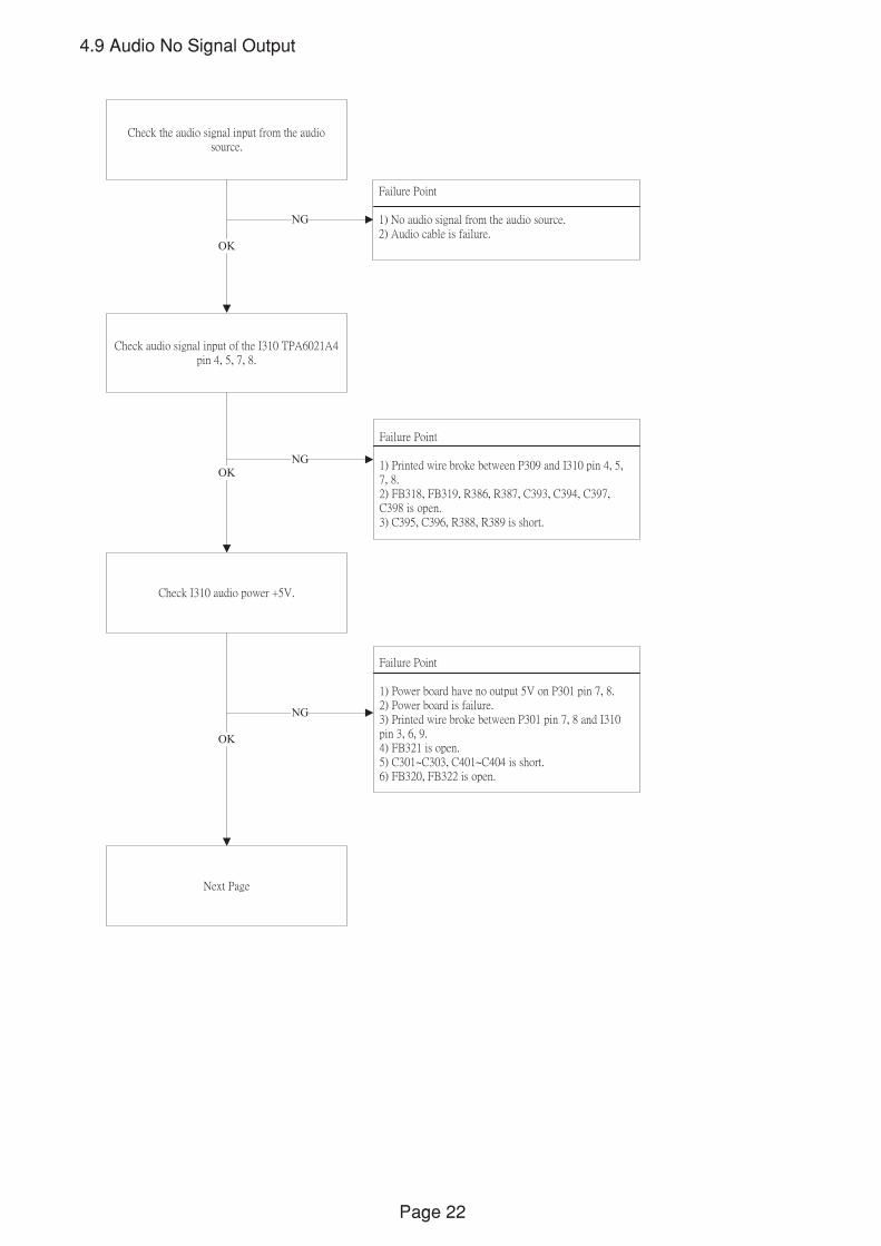
Check the audio signal input from the audio
source.
OK
NG
Failure Point
1) No audio signal from the audio source.
2) Audio cable is failure.
Check audio signal input of the I310 TPA6021A4
pin 4, 5, 7, 8.
Failure Point
1) Printed wire broke between P309 and I310 pin 4, 5,
7, 8.
2) FB318, FB319, R386, R387, C393, C394, C397,
C398 is open.
3) C395, C396, R388, R389 is short.
NG
OK
Check I310 audio power +5V.
Failure Point
1) Power board have no output 5V on P301 pin 7, 8.
2) Power board is failure.
3) Printed wire broke between P301 pin 7, 8 and I310
pin 3, 6, 9.
4) FB321 is open.
5) C301~C303, C401~C404 is short.
6) FB320, FB322 is open.
NG
OK
4.9 Audio No Signal Output
Next Page
Page 22
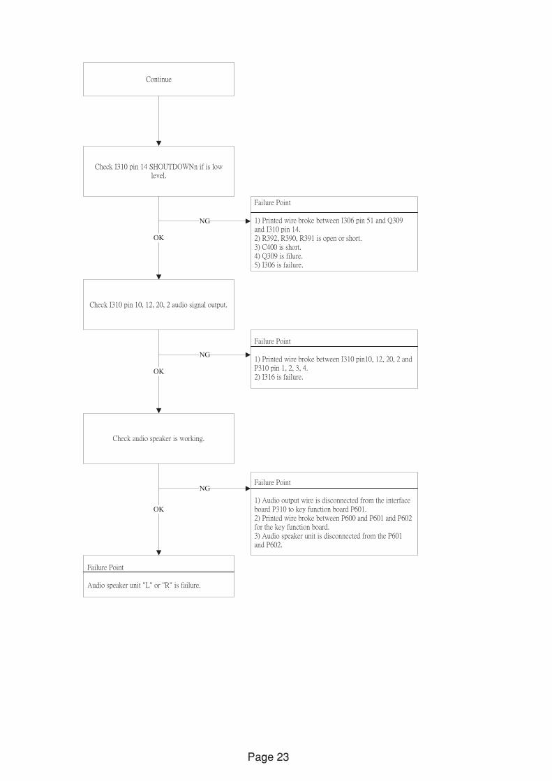
Check audio speaker is working.
OK
NGFailure Point
1) Audio output wire is disconnected from the interface
board P310 to key function board P601.
2) Printed wire broke between P600 and P601 and P602
for the key function board.
3) Audio speaker unit is disconnected from the P601
and P602.
Failure Point
Audio speaker unit "L" or "R" is failure.
Check I310 pin 14 SHOUTDOWNn if is low
level.
NG
OK
Failure Point
1) Printed wire broke between I306 pin 51 and Q309
and I310 pin 14.
2) R392, R390, R391 is open or short.
3) C400 is short.
4) Q309 is filure.
5) I306 is failure.
Continue
Check I310 pin 10, 12, 20, 2 audio signal output.
NG
OK
Failure Point
1) Printed wire broke between I310 pin10, 12, 20, 2 and
P310 pin 1, 2, 3, 4.
2) I316 is failure.
Page 23
5.S
ch
em
atic
s:
5.1
HP
_W
19
07
&W
F1
90
7_
TO
P
6A
UD
IO.
7A
UD
IO.
AU
DIO
EN
_
VO
LUM
EV
DD
2P
OW
ER
.
2P
OW
ER
.
BK
LTA
DJ
_B
KLT
EN
_P
AN
ELV
CC
EN
_
VC
C5V
VC
C3V
3
VC
C1V
8
VLC
D
VD
D
3V
GA
DD
CIN
TE
RFA
CE
.&
3V
GA
DD
CIN
TE
RFA
CE
.&
VG
AD
ET
n_
DD
CS
CL
VG
A_
_D
DC
SD
AV
GA
__
DD
CW
Pn
_ HS
IN_
VS
IN_ R
ING
ND
RG
ING
ND
GB
ING
ND
B
VC
C5V
4D
VI
DD
CIN
TE
RFA
CE
.&
4D
VI
DD
CIN
TE
RFA
CE
.&
RX
2+R
X2-
RX
1-R
X1+
RX
0-R
X0+
RX
C-
RX
C+
DD
CS
CL
DV
I_
_
DD
CW
Pn
_
DD
CS
DA
DV
I_
_
DV
ID
ET
n_
VC
C5V
HD
CP
HP
Dn
_
5S
CA
LER
GM
5726H.
5S
CA
LE
RG
M5
72
6H
.
DD
CS
CL
VG
A_
_
RIN
GIN
DD
CS
DA
VG
A_
_
BIN
HS
IN_
VS
IN_
CH
3PLV
E_
_C
H3N
LVE
__
CH
0PLV
E_
_C
H0N
LVE
__
CH
1PLV
E_
_C
H1N
LVE
__
CH
2PLV
E_
_C
H2N
LVE
__
CLK
PLV
E_
_C
LKN
LVE
__
CH
3PLV
O_
_C
H3N
LVO
__
CH
0PLV
O_
_C
H0N
LVO
__
CH
1PLV
O_
_C
H1N
LVO
__
CH
2NLV
O_
_C
H2P
LVO
__
CLK
NLV
O_
_C
LKP
LVO
__
PA
NE
LVC
CE
N_
BK
LTE
N_
BK
LTA
DJ
_
GN
DB
GN
DG
GN
DR
VG
AD
ET
n_
LED
B_
LBA
DC
IN2
_LB
AD
CIN
1_
LED
A_
DD
CW
Pn
_
AU
DIO
EN
_
VO
LUM
E
RX
2+R
X2-
RX
1+R
X1-
RX
0+R
X0-
RX
C+
RX
C-
DD
CS
CL
DV
I_
_D
DC
SD
AD
VI
__
PW
RK
EY
n_
DV
ID
ET
n_
VC
C5V
VC
C3V
3
VC
C1V
8
3V3
DV
DD
1_
HD
CP
HP
Dn
_
6K
EY
PA
NE
LIN
TE
RFA
CE
.&
6K
EY
PA
NE
LIN
TE
RFA
CE
.&
LED
B_LE
DA_
CH
3PLV
E_
_C
H3N
LVE
__
CH
2PLV
E_
_C
H2N
LVE
__
CH
1PLV
E_
_C
H1N
LVE
__
CH
0PLV
E_
_C
H0N
LVE
__
CLK
PLV
E_
_C
LKN
LVE
__
CLK
NLV
O_
_
CH
1NLV
O_
_C
H0P
LVO
__
CH
1PLV
O_
_C
H2N
LVO
__
CH
0NLV
O_
_
CH
2PLV
O_
_
CLK
PLV
O_
_
CH
3PLV
O_
_C
H3N
LVO
__
LBA
DC
IN1
_LB
AD
CIN
2_
PW
RK
EY
n_
VLC
D
VC
C5V
3V3
DV
DD
1_
CH
1NLV
OC
H1N
LVO
__
__
CH
3NLV
EC
H3N
LVE
__
__
RIN
RIN
LBA
DC
IN1
LBA
DC
IN1
__
CLK
PLV
O_
_C
LKP
LVO
__
BIN
BIN
BK
LTA
DJ
BK
LTA
DJ
__
CH
1PLV
EC
H1P
LVE
__
__
CH
3PLV
EC
H3P
LVE
__
__
HS
INH
SIN
__
CLK
NLV
OC
LKN
LVO
__
__
CH
1PLV
OC
H1P
LVO
__
__
CH
0PLV
OC
H0P
LVO
__
__
GIN
GIN
CH
3NLV
OC
H3N
LVO
__
__
CH
3PLV
O_
_C
H3P
LVO
__
DD
CS
DA
VG
AD
DC
SD
AV
GA
__
__
DD
CS
CL
VG
AD
DC
SC
LV
GA
__
__
BK
LTE
NB
KLT
EN
__
CH
2PLV
EC
H2P
LVE
__
__
CH
1NLV
EC
H1N
LVE
__
__
GN
DB
GN
DB
VS
INV
SIN
__
CH
0NLV
OC
H0N
LVO
__
__
CH
0NLV
EC
H0N
LVE
__
__
LED
BLE
DB
__
CH
2PLV
OC
H2P
LVO
__
__
CH
2NLV
EC
H2N
LVE
__
__
CH
0PLV
EC
H0P
LVE
__
__
LED
ALE
DA
__
CLK
PLV
EC
LKP
LVE
__
__
LBA
DC
IN2
LBA
DC
IN2
__
PA
NE
LVC
CE
NP
AN
ELV
CC
EN
__
GN
DG
GN
DG
CLK
NLV
EC
LKN
LVE
__
__
GN
DR
GN
DR
CH
2NLV
OC
H2N
LVO
__
__
VO
LUM
EV
OLU
ME
AU
DIO
EN
AU
DIO
EN
__
DD
CS
DA
DV
ID
DC
SD
AD
VI
__
__
DV
ID
ET
nD
VI
DE
Tn
__
RX
1R
X1
--
RX
CR
XC
++
RX
2R
X2
--
DD
CW
Pn
_
RX
2R
X2
++
VG
AD
ET
n_
VG
AD
ET
n_
RX
0R
X0
++
RX
CR
XC
--
RX
1R
X1
++
RX
0R
X0
--
DD
CS
CL
DV
ID
DC
SC
LD
VI
__
__
DD
CW
Pn
_
PW
RK
EY
nP
WR
KE
Yn
__
DD
CW
Pn
_
HD
CP
HP
Dn
HD
CP
HP
Dn
__
VC
C5V
VC
C3V
3VC
C1V
8VLC
D
VD
DV
CC
1V8
VC
C3V
3
VC
C5V
VD
D
VC
C5V
VC
C5V
3V3
DV
DD
1_
VC
C5V
VLC
D
3V3
DV
DD
1_
6832176900P
0D
12
34
56
78
91
011
12
13
12
34
56
78
91
011
12
13
ABCDEFG
ABCDEFG
PC
BN
o.
24
Go
tocover
page
HP
W1
90
7&
WF
19
07
.5
2a
HP
_W
19
07
_P
OW
ER
6832176900P
0D
D
SG
TO252
-
C
EB
TO263
-
BA
CK
LIG
HT
AD
J_
BA
CK
LIG
HT
EN
_
PA
NE
LV
CC
EN
_
BK
LT
AD
J_
BK
LT
EN
_
VC
C5
V
VC
C5
VV
LC
D
VC
C3
V3
VC
C1
V8
VC
C5
VV
CC
3V
3
VC
C5
V
VD
D
C3
13
10
uF
16
V/
T4
T6
C3
16
10
0u
F1
6V
/
R3
04
4K
7
R3
07
10
K
C3
10
10
uF
16
V/
T11
T14
C3
01
01
uF
.
T16
R3
01
1K
C3
08
01
uF
.
T8
T18
C3
14
10
0u
F1
6V
/
T7
FB
30
1P
BY
16
08
08
T6
00
YS
--
C3
11
01
uF
.
I30
1A
O3
40
11
23
T9
T1
C3
06
01
uF
.
C3
02
01
uF
.T
2
FB
30
3
PB
Y1
60
80
8T
60
0Y
S-
-
I30
3
AIC
111
71
8P
E-
1
23
4A
DJ
VO
UT
VIN
TA
B
C3
03
10
uF
16
VN
C/
()
T17
Q3
02
MM
BT
3904
2
1 3
FB
30
2P
BY
16
08
08
T6
00
YS
--
R3
08
47
K
C3
05
01
uF
.
R3
05
10
0
R3
02
10
K
R3
09
2K
4
Q3
01
MM
BT
3904
2
1 3
T13
FB
30
4
PB
Y1
60
80
8T
60
0Y
S-
-
I30
2
AIC
10
84
33
CM
-
1
23
4A
DJ
VO
UT
VIN
TA
B
T3
C3
07
10
0u
F1
6V
/
C3
12
01
uF
.
R3
06
10
KN
C(
)
T10
T15
R3
03
18
KN
C(
)
T5
C3
09
01
uF
.
P3
01
JW
TA
20
01
WR
29
P-
-
1 2 3 4 5 6 7 8 9
C3
15
10
uF
16
V/
C3
04
01
uF
NC
.(
)
T12
T19
PA
NE
LV
CC
EN
_
BK
LT
AD
J_
BK
LT
EN
_
VD
D
VC
C5
V
VC
C3
V3
VC
C1
V8
VL
CD
PC
BN
o.
12
34
56
78
91
011
12
13
12
34
56
78
91
011
12
13
ABCDEFG
ABCDEFG
25
Go
tocover
page
HP
W1
90
7&
WF
19
07

ON
OF
F-
+5V
GN
D
BR
IO
NO
FF
-
+5V
BR
I
+5V
+5V
GN
DG
ND
GN
D
GN
D
GN
D
GN
D
GN
D
GN
D
GN
D1-
GN
D
GN
D
GN
D
GN
D
GN
D
GN
D
+5V
GN
D
+2
2V
GN
DG
ND
GN
D1-
GN
D
GN
D1-
GN
D
GN
D
GN
D1-
GN
D
+2
2V
GN
D1-
GN
D
GN
D
VC
C
GN
D
GN
D1-
GN
D
GN
DV
CC
GN
D1-
GN
D
GN
D
GN
D1-
GN
D
GN
D
GN
D
GN
D1-
GN
D
GN
D
+5V
GN
D
GND 2-
GN
D2-
GN
D2-
GN
D2-
GN
D2-
GN
D2-
GN
D2-
GN
D2-
GN
D2-
GN
D2-
GN
D2-
GN
D
GN
D
R8
07
33.
D1
20
1N
41
482
1
VR
80
11
0K Q
80
3
7N
65
C1
23
R11
7
10
0K
1%
C11
21
0P
3K
V/
C8
09
0 01u 1KV. /
R8
02
SC
K0
83
T801
ET
20
-
1 3
2 4
+C
10
222uF 50V/
12
D1
08
1N
41
48
21
+C
81
8
47
0U
35
V/
D1
05
*
1
R8
04
15
K
C1
04
33
0P
NP
O
R8
29
12
0K
08
05
/
12
2P
P1
02
12
R1
26
33
K1
.%
R11
3
10
K
C1
34
10
uF
12
06
X5
R/
/
D8
07
18
B
1
Q1
05
AO
D4
54
3 2
1
+C
10
3
2 2uF 50V. /
12
R1
21
10
0K
1%
R8
22
30
0K
08
05
/
P8
01
132
LGN
+ C8
29
1uF 50V/
12
R1
37
1K
08
05
/
C1
01
0 1uF.
+ C8
05
100U 450V/
C8
12
33
nF
D8
11
27
B
1
C8
08
00
1u
1K
V.
/
R1
04
51
0K
D1
07
1N
41
48
21
C8
03
*
R8
18
91
02
W/
R8
31
33
K1
%
+C
82
4
10
00
U1
0V
/
R1
39
1K
08
05
/
R1
05
22
D1
21
1N
41
48
2 1
R1
07
56
K.
T802
ER
28
21
0
15 4
6 97
3
C11
9
47
0P
X7
R
C11
4
5P
3K
V/
C1
30
10
00
P
L8
04
JU
MP
ER
WIR
E
C11
61
0P
3K
V/
R8
16
0
R8
09
10
0K
C8
06
0 01uF 630V. /
D8
03
PR
10
07
G
R11
5
33
K1
.%
R8
24
33
K1
%
R1
02
30
1K
.
R8
19
1K
MO
F/
C8
25
33
00
P2
50
VY
/-
C8
16
10
00
P
50
0V
X7
R
C1
28
00
1u
F.
..
..
T101
EE
L2
2
7263
51 48
54 3
876
2 1
IS
VCC
GND
PRCT
CTRL
DRAIN
HVSPACE
GDRV
I80
1
TE
A1530
R1
36
10
K
+
C1
25
22
0u
F3
5V
/
12
C8
01
0 47U 275V. /
R8
14
22
MO
F/
R1
22
15
K1
%
I10
1
OZ
99
38
8 7 6 5 1234
9 10
11
12
13
14
15
16
NC
OV
PT
VS
EN
ISE
N
DR
V1
VD
DA
TIM
ER
DIM
NC
EN
A
LC
T
SS
TC
MP
CT
GN
DA
DR
V2
PG
ND
R8
21
30
0K
08
05
/
D11
71
N4
14
8
2 1
R8
30
68
K0
80
5/
Q8
06
39
04
2
1 3
+C
82
31
00
0U
10
V/
R1
01
10
K
R8
15
47
KM
OF
./
R1
33
22
R1
40
1K
08
05
/
I80
3
AP
43
11
%1A 2C
3R
F8
01
31
5A
H2
50
V.
R11
9
15
K1
%
R8
25
1K
D11
6
1N
41
48 2
1
R1
03
18
K
R1
25
3M
14
W/
Q1
01
2N
70
02
1
23
R8
11
02
72
W.
/
D11
21
N4
14
8
21
+C
82
61uF 50V/
12
R1
31
22
R8
33
10
0
+C
81
7
47
0U
35
V/
C111
10
00
P
R8
32
47
K1
.%
D1
03
*
1
R1
28
51
K.
+C
82
2
10
00
U1
0V
/
+
C11
02
2u
F5
0V
./
12
C8
11
02
2u
F.
12
2P
P1
03
12
D1
01
SB
14
0
R8
27
15
K1
.%
D8
12
1N
41
48 2
1
-+
D8
01
GB
U4
08
2
4
3
1
R11
63
M1
4W
/
12
2P
P1
01
12
R1
38
1K
08
05
/
12
2P
P1
04
12
R11
8
56
K
D11
31
N4
14
8
21
R8
05
10
0K
2W
/
R1
35
1M
C1
22
10
uF
12
06
X5
R/
/
R8
23
27
0
R111
49
91
%
C8
27
00
1u
F.
R8
28
1K
+
C1
24
22
0u
F3
5V
/
12
C1
31
22
nF
R1
20
51
K.
R8
20
300K 0805/L
80
2
10
U
C8
20
33
00
P2
50
VY
/-
R1
30
49
91
%
C8
10
10
0P
1K
VX
7R
C8
21
10
00
P1
00
VX
7R
R8
08
13
K
Q1
03
39
06
3
1
2
C1
06
00
47
uF
.
R1
34
2K
08
05
/
D8
04
1N
49
37
21
D11
81
N4
14
821
P8
02
8 7 6 5 4 3 2 1910
R1
06
150K 1%
C8
15
00
1u
F.
1K
V
Q1
02
39
04
3
1
2
D8
10
SB
F1
04
5C
T2
31
C1
05
10
00
P
D1
04
*
1
C8
14
01
uF
.
L8
03
BE
AD
6m
m/
+C
82
8
22
uF
50
V.
/
C1
09
00
1u
F.
D11
41
N4
14
821
C8
19
0 1U 275V. /
C8
13
02
2u
F.
D1
02
SB
14
0
C8
04
*
C11
8
5P
3K
V/
Q1
04
AO
D4
13
2 3
1
D8
09
ST
PF
10
20
CT
231
R8
03
05
1.
1W
MO
F
C8
02
22
00
P2
50
V/
C1
23
10
uF
12
06
X5
R/
/
L8
01
BE
AD
6m
m/
C8
32
22
00
P2
50
V/
R8
06
47
5K
1.
%
R8
13
10
0M
OF
/
I80
2
LT
V817
123 4
D1
06
1N
41
482
1
+C
80
7
82
uF
35
V/
12
R8
17
1K
R8
26
1K
D8
06
1N
41
482
1
D1
09
1N
41
482
1
C11
5
47
0P
X7
R
R1
32
2K
08
05
/
.5
2b
HP
_W
F1
90
7_
PO
WE
R
6832180800-0
BP
CB
No
.
12
34
56
78
91
011
12
13
12
34
56
78
91
011
12
13
ABCDEFG
ABCDEFG
26
Go
tocover
page
HP
W1
90
7&
WF
19
07
huicho
Nota
capacitor en corto, no aparecia vcc
.5
3H
P_
W1
90
7&
WF
19
07
_V
GA
DD
CIN
TE
RF
AC
E&
PC
BN
o.
6832176900P
0D
DD
CS
DA
VG
A_
_
VG
A5
V_
VG
A5
V_
VG
AB
LU
E_
VG
AR
ED
_
VG
AG
RE
EN
_
VG
AV
SY
NC
_
VG
AH
SY
NC
_
VG
AC
ON
n_
DD
CS
CL
VG
A_
_D
DC
SD
AV
GA
__
HS
IN
BL
UE
IN_
GR
EE
NIN
_
VG
AS
DA
_
DD
CS
CL
VG
A_
_
VG
AS
CL
_
DD
C5
VA
_
VG
AD
ET
n_
RE
DIN
_
GN
DB
GN
DG
GN
DR
RIN
GIN
BIN
VG
AC
ON
n_
VS
IN
DD
CS
DA
VG
A_
_D
DC
SC
LV
GA
__
DD
CW
Pn
_V
GA
SC
L_
VG
AS
DA
_
VC
C5
V
VC
C5
VV
CC
5V
VC
C5
V
VC
C5
V
C3
22
01
uF
.
T24
T39
R3
24
2K
4
T20
C3
27
22
0p
F
R3
30
2K
4
P3
02
CO
NN
EC
TO
RD
B1
5
8 15
7 14
6 13
5 12
4 11
3 10
2 9 1
16 17
T55
I30
4
24
C0
2
12345 6 7 8
A0
A1
A2
GN
DS
DA
SC
LW
PV
CC
C3
23
01
uF
.
T57
R3
13
75
1/%
T37
T25
D3
08
MM
SZ
5232B
FB
30
50
D3
10
MM
SZ
5232B
C3
30
01
uF
.
T43
T3
3
R3
29
47
T54 T
40
FB
30
6S
BK
16
08
08
T6
00
YS
--
R3
11
10
0
D3
06
MM
SZ
5232B
R3
14
75
1/%
R3
22
10
0
T38
T30
C3
19
10
nF
FB
31
2
SB
K1
60
80
8T
45
1Y
S-
-
D3
05
MM
SZ
5232B
T51
C3
31
47
pF
T53
D3
09
MM
SZ
5232B
T36
R3
16
10
0
T45
FB
30
8S
BK
16
08
08
T6
00
YS
--
C3
24
10
nF
T46
FB
31
0S
BK
16
08
08
T6
00
YS
--
T26
C3
18
10
nF
R3
17
75
1/%
T21
C3
28
22
0p
F
R3
18
10
0
R3
10
75
1/%
C3
20
10
nF
T31
T44
T56
T4
9
R3
21
10
0
T22
T27
D3
01
MM
BD
7000
3
1
2
R3
27
12
K
D3
04
MM
SZ
5232B
C3
29
01
uF
.
C3
26
01
uF
.
C3
21
01
uF
.
Q3
03
MM
BT
3904
2
1 3
T47
T50
R3
15
75
1/%
T29
R3
25
10
K
R3
23
2K
4
T28
T42
FB
311
SB
K1
60
80
8T
45
1Y
S-
-
C3
25
10
nF
T34
R3
26
12
K
R3
19
10
K
T35
D3
07
BA
T5
4C
T52
R3
12
75
1/%
FB
30
70
D3
03
MM
BD
70
00
3
1
2
T32
T48
T23
T4
1
C3
17
10
nF
D3
02
MM
BD
7000
3
1
2
R3
20
1K
R3
28
47
C3
32
47
pF
FB
30
90
RIN
GN
DR
BIN
GN
DB
VG
AD
ET
n_
DD
CS
CL
VG
A_
_D
DC
SD
AV
GA
__
VS
IN_
HS
IN_
GIN
GN
DG
DD
CW
Pn
_
VC
C5
V
12
34
56
78
91
011
12
13
12
34
56
78
91
011
12
13
ABCDEFG
ABCDEFG
27
Go
tocover
page
HP
W1
90
7&
WF
19
07
.5
4H
P_
W1
90
7&
WF
19
07
_D
VI
DD
CIN
TE
RF
AC
E&
PC
BN
o.
68
32
17
69
00
P0
D
DV
IR
X2
_+
DV
IH
P_
DV
IR
X1
_+
DV
IS
DA
_D
VI
SC
L_
DV
IR
X0
_-
DV
I5
V_
DV
I5
V_
DV
IC
ON
n_
DD
CW
Pn
_
DD
C5
VD
_
DV
IS
CL
_
DV
I5
V_
DD
C5
VD
_
DV
IR
X2
_-
DV
IR
X0
_-
DV
IR
XC
_+
DV
IR
X1
_-
DV
IR
X1
_+
DV
IC
ON
n_
DV
IR
X2
_+
DV
IR
X2
_-
DV
IR
X0
_+
DV
IR
X0
_+
DD
CS
DA
DV
I_
_D
DC
SC
LD
VI
__
DD
CS
CL
DV
I_
_
DD
CS
DA
DV
I_
_D
DC
SC
LD
VI
__
DV
IR
XC
_-
DV
IR
X1
_-
DV
IR
XC
_+
DV
IR
XC
_-
RX
C-
RX
C+
RX
0-
RX
2-
DV
ID
ET
n_
RX
2+
RX
1-
RX
1+
RX
0+
DV
IS
DA
_
DD
CS
DA
DV
I_
_
HD
CP
HP
Dn
_
VC
C5
V
VC
C5
VV
CC
5V
VC
C5
VV
CC
5V
VC
C5
V
VC
C5
VV
CC
5V
VC
C5
VV
CC
5V
Q3
04
MM
BT
3904
2
1 3
R3
37
1K
T101
R3
32
10
1/%
T82
C3
44
01
uF
.
D3
18
MM
BD
70
00
3
1
2
C3
36
01
uF
.
R3
41
10
1/%
T68
T5
9
T80
C3
40
01
uF
.
T72
P3
03
DV
ID-
12345678910
11
12
13
14
15
16
17
18
19
20
21
22
23
24
C1
C2
C3
C4
C5
RX
2-
RX
2+
GN
DR
X4
-R
X4
+S
CL
SD
AV
S
RX
1-
RX
1+
GN
DR
X3
-R
X3
+5
VG
ND
HP
RX
0-
RX
0+
GN
DR
X5
-R
X5
+G
ND
RX
C+
RX
C-
28
27
RE
DG
RN
BL
UH
SG
ND
29
30
31
32
D3
21
MM
SZ
5232B
T60
D3
13
MM
BD
70
00
3
1
2
C3
41
01
uF
.
Q3
05
MM
BT
3904
2
1 3
C3
43
01
uF
.
C3
37
10
0u
F1
6V
NC
/(
)D
311
MM
BD
70
00
3
1
2
T64
R3
31
10
K
T83
T7
8
R3
33
10
1/%
T65
C3
38
01
uF
.
D3
17
MM
BD
70
00
3
1
2
T70
D3
19
MM
BD
70
00
3
1
2
R3
44
10
K
R3
34
10
1/%
D3
23
MM
SZ
5232B
R3
45
2K
4
C3
34
01
uF
.
T85
T7
7
T61
D3
16
MM
BD
70
00
3
1
2
T58
T79
T6
2
R3
47
47
R3
36
1K
R3
35
10
1/%
R3
61
2K
4
R3
43
12
K
D3
15
MM
SZ
5232B
I30
5
24
C0
2
12345 6 7 8
A0
A1
A2
GN
DS
DA
SC
LW
PV
CC
C3
33
01
uF
.
T76
T63
T66
D3
14
MM
BD
70
00
3
1
2
C3
42
01
uF
.
T74
R3
39
10
1/%
T176
R3
46
47
T84
D3
20
BA
T5
4C
C3
46
47
pF
C3
45
01
uF
.
T69
R3
38
10
1/%
C3
35
01
uF
.
D3
12
MM
BD
70
00
3
1
2
T75
T73
R3
40
10
1/%
T67
C3
39
01
uF
.
C3
47
47
pF
T71
R3
42
12
K
T81
D3
22
MM
SZ
5232B
RX
2+
RX
2-
RX
1-
RX
1+
RX
0-
RX
0+
RX
C-
RX
C+
DV
ID
ET
n_
DD
CS
CL
DV
I_
_
DD
CW
Pn
_
DD
CS
DA
DV
I_
_
VC
C5
V
HD
CP
HP
Dn
_
12
34
56
78
91
011
12
13
12
34
56
78
91
011
12
13
ABCDEFG
ABCDEFG
28
Go
tocover
page
HP
W1
90
7&
WF
19
07
.5
5H
P_
W1
90
7&
WF
19
07
_S
CA
LE
RG
M5
72
6H
PC
BN
o.
6832176900P
0D
PIN51
HJTAGportdisableLJTAGportenable
:-
,:
-.
PIN119
HUARTonGPOLUARTonDDC
:,
:.
PIN50
HUseATMELSPIROMLUseStandardSPIROM
:,
:.
PIN56
HUseOSCLUseXtal
:,
:.
PIN57
HInternalROMoffLInternalROMon
:,
:.
PIN58
Settolow
.
DD
CS
CL
VG
AD
DC
SC
LV
GA
__
__
DD
CS
DA
VG
AD
DC
SD
AV
GA
__
__
SP
IH
OL
Dn
_S
PI
WP
n_
SP
ID
O_
RE
XT
CH
1P
LV
O_
_
SP
IC
LK
IN_
_
CH
3N
LV
O_
_C
LK
PLV
O_
_
SP
IC
LK
_
BK
LT
AD
J_
CH
0N
LV
O_
_
TC
LK
BK
LT
EN
_
ICR
ES
ET
n_
CH
1N
LV
O_
_
GN
DB
GN
DB
CH
2N
LV
O_
_
HS
INH
SIN
__
XTA
L
RIN
RIN
UA
RT
DO
_
CH
3P
LV
O_
_
BIN
BIN
PA
NE
LV
CC
EN
_V
OL
UM
E
CH
0P
LV
O_
_
GIN
GIN
SP
ID
I_
UA
RT
DI
_
VS
INV
SIN
__
CL
KN
LV
O_
_C
H2
PLV
O_
_
GN
DG
GN
DG
GN
DR
GN
DR
SP
ID
I_
SP
ID
O_
CH
3N
LV
E_
_C
LK
PLV
E_
_
CH
1N
LV
E_
_
CH
2N
LV
E_
_
CL
KN
LV
E_
_
CH
0P
LV
E_
_
CH
3P
LV
E_
_
CH
0N
LV
E_
_
CH
2P
LV
E_
_
CH
1P
LV
E_
_
DD
CS
DA
DV
ID
DC
SD
AD
VI
__
__
DD
CS
CL
DV
ID
DC
SC
LD
VI
__
__
RX
2R
X2
++
RX
2R
X2
--
RX
1R
X1
++
RX
1R
X1
--
RX
0R
X0
++
RX
0R
X0
--
RX
CR
XC
++
RX
CR
XC
--
SP
IC
Sn
_
UA
RT
DO
_
UA
RT
DI
_V
OL
UM
E
BK
LT
AD
J_
AU
DIO
EN
AU
DIO
EN
__
GP
O5
_
LE
DA
_L
ED
B_
ICR
ES
ET
n_
SD
AS
CL
LB
AD
CIN
1_
LB
AD
CIN
2_
LB
AD
CIN
1_
LB
AD
CIN
2_
PW
RK
EY
n_
PW
RK
EY
n_
SD
A
DD
CW
Pn
_
SC
LV
GA
DE
Tn
_D
VI
DE
Tn
_
HD
CP
HP
Dn
_
SP
IC
Sn
_
3V
3A
VD
D_
VC
C3
V3
VC
C1
V8
VC
C1
V8
1V
8C
VD
D_
3V
3D
VD
D_
VC
C3
V3
3V
3R
PL
L_
VC
C3
V3
3V
3R
PL
L_
VC
C5
V
3V
3A
VD
D_
3V
3R
PL
L_
3V
3A
VD
D_
1V
8A
VD
D_
1V
8A
VD
D_
1V
8C
VD
D_
3V
3D
VD
D_
VC
C5
V
VC
C3
V3
3V
3D
VD
D_
3V
3D
VD
D_
VC
C3
V3
VC
C3
V3
3V
3D
VD
D1
_
3V
3D
VD
D1
_
C3
69
01
uF
.
R3
58
2K
4
C3
81
01
uF
.
C3
82
01
uF
.
C3
60
01
uF
.
C3
70
01
uF
.
T1
02
R3
54
2K
4
T93
T105
R3
59
4K
7
T94
R3
55
2K
4
C3
61
01
uF
.
R3
67
82
0K
C3
54
01
uF
.C
35
8
01
uF
.
I30
6
gm
57
26
HP
QF
P1
28
-
99
10
09
69
79
39
4
73
72
76
75
81
80
10
81
09
12
31
24
12
51
26
38
37
84
83
69
59
60
64
65
66
67
111
12
11
22
12
74
9
89
90
5488117
63
30
29
18
28
36
35
24
21
23
22
20
19
27
6 5 4 339
40
42
33
34
31
32
15
16
41
11
12
910
7814
13
51
56
57
58
50
11
9
12
0
11
511
411
311
2
110
10192
8274
12
8
22547
5391
116
118875517
86
7870
104
106
43
44
45
46
10
5
68717779
9598102
107
2648
1
85
103
52
61
62
RE
D+
RE
D-
GR
EE
N+
GR
EE
N-
BL
UE
+B
LU
E-
RX
2-
RX
2+
RX
1-
RX
1+
RX
0-
RX
0+
XTA
LT
CL
KG
PIO
11
DA
TA
3_
/[
]G
PIO
12
VD
ATA
4_
/[
]G
PIO
13
VD
ATA
5_
/[
]G
PIO
14
VD
ATA
6_
/[
]
CH
1N
LV
OD
CL
K_
_/
CH
1P
LV
OD
VS
__
/
RX
C-
RX
C+
RE
XT
SP
IC
Sn
_S
PI
CL
K_
DD
CS
CL
VG
AG
PIO
16
__
/_
DD
CS
DA
VG
AG
PIO
17
__
/_
DD
CS
CL
DV
IG
PIO
18
__
/_
DD
CS
DA
DV
IG
PIO
19
__
/_
RE
SE
Tn
GP
IO9
VD
ATA
1_
/[
]G
PIO
10
VD
ATA
2_
/[
]
PP
WR
PB
IAS
HS
YN
CV
SY
NC
CRVSSCRVSSCRVSS
RV
DD
33
_
PD
19
GP
O3
9/
PD
18
GP
O3
8/
CRVSS
PD
17
GP
O3
7/
CH
2N
LV
OD
HS
__
/C
H2
PLV
OD
EN
__
/
PD
14
GP
O3
5/
PD
12
GP
O3
2/
PD
14
GP
O3
4/
PD
13
GP
O3
3/
PD
11
PD
10
VF
IEL
D/
_
PD
16
GP
O3
6/ V
DE
IN_
VV
SIN
_V
HS
IN_
VC
LK
IN_
CH
0P
LV
O_
_C
H0
NLV
O_
_
GP
IO2
5_
CL
KP
LV
OP
D2
2_
_/
CL
KN
LV
OP
D2
3_
_/
CH
3P
LV
OP
D2
0_
_/
CH
3N
LV
OP
D2
1_
_/
CH
0N
LV
EP
D8
__
/C
H0
NLV
EP
D9
__
/
GP
IO2
4_
CH
2P
LV
EP
D4
__
/C
H2
NLV
EP
D5
__
/
CL
KP
LV
EP
D2
__
/C
LK
NLV
EP
D3
__
/
CH
3P
LV
EP
D0
__
/C
H3
NLV
EP
D1
__
/
CH
1N
LV
EP
D7
__
/C
H1
PLV
EP
D6
__
/
GP
O0
PW
M2
_/
GP
O1
PW
M3
_/
GP
O2
_G
PO
3_
GP
O4
PW
M0
_/
GP
O5
PW
M1
_/
GP
IO8
VD
ATA
0_
/[
]
LB
AD
CIN
1G
PIO
20
_/
_L
BA
DC
IN2
GP
IO2
1_
/_
LB
AD
CIN
3G
PIO
22
_/
_L
BA
DC
VS
S_
AVDD RPLL 33_ _
AVDD ADC 33_ _AVDD ADC 33_ _
AVDD DVI 33_ _AVDD DVI 33_ _
GP
IO1
5V
DA
TA
7_
/[
]
VDD OUT 33_ _VDD OUT 33_ _VDD OUT 33_ _
RVDD 33_RVDD 33_
LBADC VDD 33_ _
CVDD 18_CVDD 18_CVDD 18_CVDD 18_
GP
IO3
1_
AVDD DVI 18_ _AVDD DVI 18_ _
AVDD ADC 18_ _
VDD RPLL 18_ _
GP
IO2
6_
GP
IO2
7_
GP
IO2
8_
IRIN
GP
IO2
9_
/_
VB
UF
CR
PL
L_
AVSS DVI_AVSS DVI_AVSS DVI_AVSS DVI_
AVSS ADC_AVSS ADC_AVSS ADC_
AVSS RPLL_
VSS OUT_VSS OUT_
AVSS BIAS_
GP
IO3
0_
AVSS ADC_
CRVSS
SP
ID
I_
SP
ID
O_
C3
78
01
uF
NC
.(
)
C3
73
10
pF
FB
31
4
PB
Y1
60
80
8T
30
1Y
S-
-
T86
R3
50
25
01/
%
X301
14
31
8M
HZ
.
FB
31
6
PB
Y1
60
80
8T
30
1Y
S-
-
C3
66
01
uF
.
R3
64
10
KI3
08
24
LC
16
B
12345 6 7 8
A0
A1
A2
GN
DS
DA
SC
LW
PV
CC
C3
62
10
pF
C3
77
01
uF
.
R3
53
2K
4N
C(
)
T95
T9
2
C3
53
01
uF
.
C3
49
01
uF
.
T87
C3
57
10
uF
16
V/
T103
C3
76
01
uF
.
FB
32
3
PB
Y1
60
80
8T
30
1Y
S-
-
FB
31
7
PB
Y1
60
80
8T
30
1Y
S-
-
R3
62
10
K
C3
67
01
uF
.
T100
C3
65
01
uF
.
P3
04
JW
TA
20
01
WV
20
4N
C-
-(
)
1234
R3
60
4K
7
T1
06
T88
T9
1
C3
59
01
uF
.
R3
63
2K
4
C3
75
10
0p
F
R3
69
82
0K
C3
64
01
uF
.
FB
31
3
PB
Y1
60
80
8T
30
1Y
S-
-
C3
68
10
uF
16
V/
C3
74
01
uF
.
C3
52
01
uF
.
R3
65
10
0
T1
08
R3
57
2K
4
T1
07
T99
C3
56
01
uF
.
T89
I30
9
SS
T2
5V
F0
20
A
12345 6 7 8
CE
#S
OW
P#
GN
DS
IS
CK
HO
LD
#V
CC
R3
48
2K
4
C3
80
01
uF
.
C3
48
10
uF
16
V/
C3
72
01
uF
.
C3
83
01
uF
.
C3
79
01
uF
.
R3
51
2K
4
C3
71
01
uF
.
T96
T1
09
I30
7
ST
L8
11
0G
NL
46
3F
NL
H(
)
1 2 3
GN
D
RS
T
VC
C
C3
55
10
uF
16
V/
R3
49
10
1/%
C3
63
10
uF
16
V/
T98
C3
51
01
uF
.
R3
66
10
0
R3
68
82
0K
T90
T104
FB
31
5
PB
Y1
60
80
8T
30
1Y
S-
-
R3
52
2K
4N
C(
)
R3
56
2K
4
T97
C3
50
01
uF
.
PA
NE
LV
CC
EN
_B
KLT
EN
_
CH
3P
LV
O_
_C
H3
NLV
O_
_
CL
KN
LV
O_
_C
LK
PLV
O_
_
CH
0N
LV
O_
_
CH
2N
LV
O_
_C
H1
PLV
O_
_
CH
0P
LV
O_
_C
H1
NLV
O_
_
CH
2P
LV
O_
_
RIN
GN
DR
GIN
GN
DG
BIN
GN
DB
HS
IN_
VS
IN_
DD
CS
CL
VG
A_
_D
DC
SD
AV
GA
__
BK
LT
AD
J_
CH
1N
LV
E_
_
CH
3P
LV
E_
_
CH
1P
LV
E_
_
CL
KP
LV
E_
_C
LK
NLV
E_
_
CH
0P
LV
E_
_
CH
2N
LV
E_
_
CH
3N
LV
E_
_
CH
2P
LV
E_
_
CH
0N
LV
E_
_
DD
CS
CL
DV
I_
_D
DC
SD
AD
VI
__
RX
2+
RX
2-
RX
1-
RX
1+
RX
0-
RX
0+
RX
C-
RX
C+
VO
LU
ME
AU
DIO
EN
_
LE
DA
_L
ED
B_
LB
AD
CIN
1_
LB
AD
CIN
2_
PW
RK
EY
n_
VC
C5
V
VC
C3
V3
VC
C1
V8
VG
AD
ET
n_
DV
ID
ET
n_
DD
CW
Pn
_
3V
3D
VD
D1
_
HD
CP
HP
Dn
_
12
34
56
78
91
011
12
13
12
34
56
78
91
011
12
13
ABCDEFG
ABCDEFG
29
Go
tocover
page
HP
W1
90
7&
WF
19
07
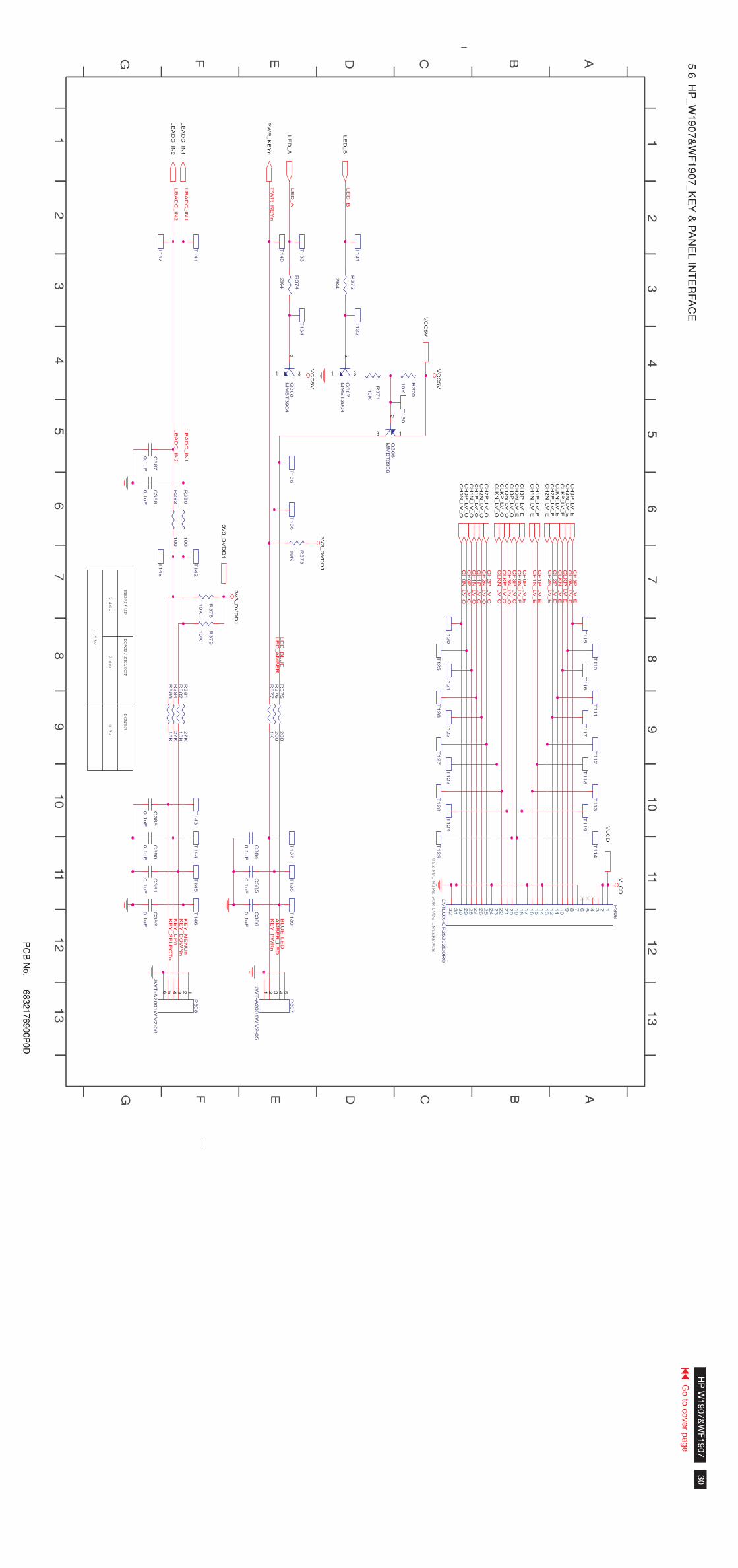
.5
6H
P_
W1
90
7&
WF
19
07
_K
EY
PA
NE
LIN
TE
RF
AC
E&
PC
BN
o.
USEFFCWIREFORLVDSINTERFACE
MENU
UP
DOWN
SELECT
POWER
//
246V
200V
..
163V
.
03V
.
LE
DB
_
LE
DA
_
BLU
ELE
D_
LE
DB
LU
E_
KE
YM
EN
Un
_K
EY
DO
WN
n_
KE
YU
Pn
_K
EY
SE
LE
CT
n_
AM
BE
RLE
D_
KE
YP
WR
n_
PW
RK
EY
n_
CH
2N
LV
E_
_
CH
0P
LV
E_
_
CH
2P
LV
O_
_
CH
1N
LV
O_
_
CLK
PLV
E_
_
CH
3P
LV
O_
_C
H0N
LV
E_
_
CH
3N
LV
E_
_
CH
3N
LV
O_
_
CH
3P
LV
E_
_
CLK
PLV
O_
_
CH
1P
LV
O_
_
CH
1P
LV
E_
_
CH
2P
LV
E_
_
CH
0P
LV
O_
_C
H0N
LV
O_
_
CLK
NLV
O_
_
CH
2N
LV
O_
_
CLK
NLV
E_
_
CH
1N
LV
E_
_
LE
DA
MB
ER
_
LB
AD
CIN
1_
LB
AD
CIN
2_
LB
AD
CIN
2_
LB
AD
CIN
1_
VC
C5V
VC
C5V
VLC
D
3V
3D
VD
D1
_
3V
3D
VD
D1
_
T120
C386
01uF
.
T115
T135
T145
T125
R379
10
K
R372
2K
4
T110
T126
T140
T141
Q30
8M
MB
T3904
2
1 3
T121
T139
T111
C389
01uF
.
R374
2K
4
T137
T127
T132
T116
R371
10
K
T142
T138
R375
20
0
Q30
7M
MB
T3904
2
1 3
C390
01uF
.
T122
R376
20
0
C391
01uF
.
T112
P30
8
JW
TA
2001W
V2
06
--
123456
T128
T144
R380
100
T117
R370
10
K
T134
C384
01uF
.
R382
15
K
T148
P30
7
JW
TA
2001W
V2
05
--
1 2 3 4 5
T123
P306
CV
ILU
XC
F25302D
0R
0-
12345678910
11
12
13
14
15
16
17
18
19
20
21
22
23
24
25
26
27
28
29
30
31
32
T143
C385
01uF
.
T113
T147
R384
27
K
C392
01uF
.
R381
27
K
T129
T118
T131
R378
10K
R377
1K
T130
T124
T114
T136
C387
01uF
.
R383
100
T119
R385
15
K
T146
T133
Q30
6M
MB
T3906
3
2
1
C388
01uF
.
R373
10
KLE
DA
_
LE
DB
_
PW
RK
EY
n_
LB
AD
CIN
1_
LB
AD
CIN
2_
VC
C5V
3V
3D
VD
D1
_
CH
2P
LV
E_
_
CH
3P
LV
E_
_
CH
1P
LV
E_
_
CLK
NLV
E_
_
CH
2N
LV
E_
_
CH
3N
LV
E_
_C
LK
PLV
E_
_
CH
0P
LV
E_
_C
H0N
LV
E_
_
CH
1N
LV
E_
_
CH
3N
LV
O_
_
CH
1P
LV
O_
_
CLK
NLV
O_
_
CH
0P
LV
O_
_
CH
2N
LV
O_
_
CH
1N
LV
O_
_
CLK
PLV
O_
_
CH
3P
LV
O_
_
CH
0N
LV
O_
_
CH
2P
LV
O_
_
VLC
D
6832176900P
0D
12
34
56
78
91
011
12
13
12
34
56
78
91
011
12
13
ABCDEFG
ABCDEFG
30
Go
tocover
page
HP
W1
90
7&
WF
19
07
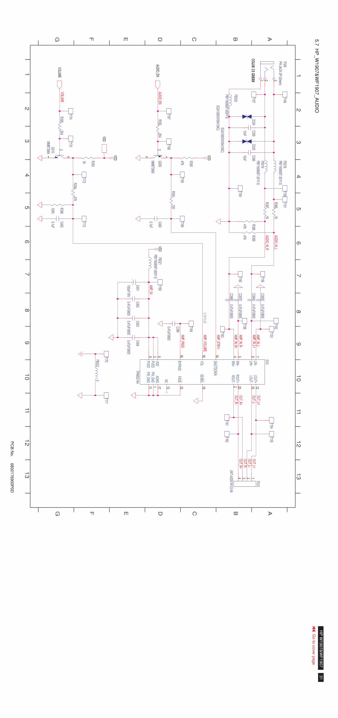
.5
7H
P_
W1
90
7&
WF
19
07
_A
UD
IO
PC
BN
o.
6832176900P
0D
COLORIS
GREEN
03V36V
.~
.AM
PVO
LUME
_
OUT
R_-
AMP
STBYn_
OUT
L_-
OUT
R_+O
UTR_-
AUDIOEN
_
OUT
L_+O
UTL_-
AMP_PASS
AUDIOIN
R_
_
AMP
INR
__
+
AUDIOIN
L_
_
VOLUM
E
OUT
L_+
OUT
R_+
AMP
INL
__
-AM
PIN
L_
_+
AMP
INR
__
-
AMP
5V_
VDD
VDD
VDD
T154
T151
C396
10nF FB319PBY160808T
301YS
--
T159
R3861K
T160
T166
C3970
47uF0805
./
T169
T155
FB318PBY160808T
301YS
--
T174
Q309
MM
BT3906
3
2
1
T149
C3940
47uF0805
./
I310
TPA6021A4
3 5 710
18 812
9 14
201716
11
4219
161513
PVDD
RIN-
LIN-LO
UT-
VOL
LIN+LO
UT+
PVDD
SHUTDOW
N ROUT+
AGND
PWG
ND_
VDD
PWG
ND_
RINRO
UT+
-
SEBEL
/
BYPASSFADENC
T170
Q310
MM
BT3904
2
1 3
R393
1K
C404
047uF
0805.
/
R3871K
T168
T163
D325
EGA10603V05A1
NC(
)
T156
FB3220
T175
R3922K4
T164
T150
R39447K
R390
47K
T158
T161
C400
01uF.
C395
10nF
T157
C403
047uF
0805.
/
T171
T172
C3980
47uF0805
./
T162
C405
01uF.
T165
T153
C399
047uF
0805.
/
FB320
PBY160808T600Y
S-
-
R388
47K
C401
100uF16V/
R391100
R389
47K
D324
EGA10603V05A1
NC(
)
T173
P310
JWT
A2001WV2
04-
-
1234
C402
047uF
0805.
/
T152
R3952K4
R396
100K
C3930
47uF0805
./
P309PH
JACK3P
Green
--
()
321
T167
FB321PBY160808T
600YS
--
VDD
VOLUM
E
AUDIOEN
_ 12
34
56
78
91
011
12
13
12
34
56
78
91
011
12
13
ABCDEFG
ABCDEFG
31
Go
tocover
page
HP
W1
90
7&
WF
19
07
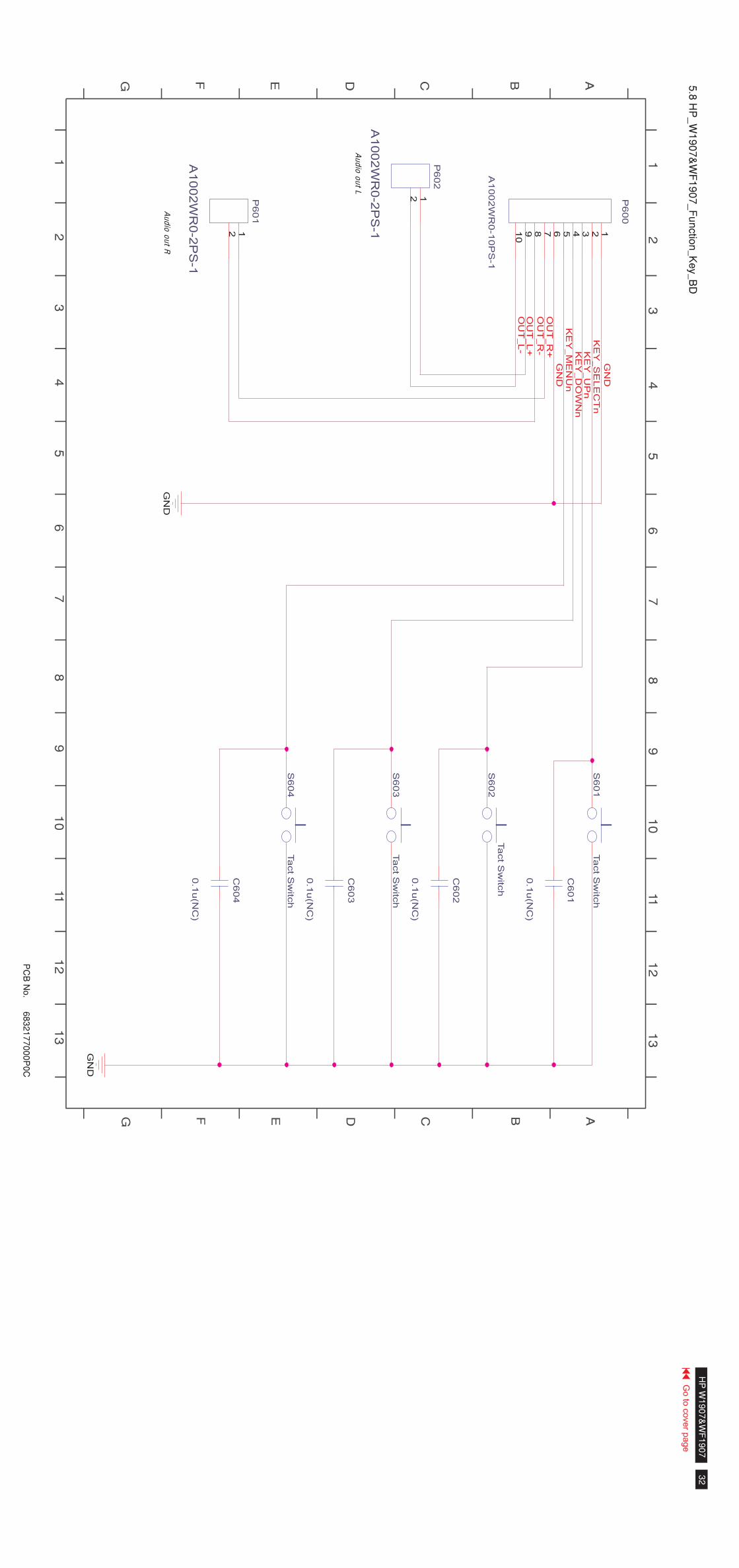
.5
8H
P_
W1
90
7&
WF
19
07
_F
un
ctio
nK
ey
BD
__
PC
BN
o.
68
32
17
70
00
P0
C
Audio
outR
Audio
outL
KE
YS
ELE
CT
n_
KE
YU
Pn
_
OU
TL
_+
OU
TL
_-
OU
TR
_+
KE
YM
EN
Un
_ KE
YD
OW
Nn
_
GN
D
GN
D
OU
TR
_-
GN
D
GN
D
S601
TactS
witc
h
P601
A1002W
R0
2P
S1
--
12
C603
01u
NC
.(
)
S602
TactS
witc
h
S603
TactS
witc
h
C604
01u
NC
.(
)
S604
TactS
witc
h
C601
01u
NC
.(
)
P600
A1002W
R0
10P
S1
--
12345678910
P602
A1002W
R0
2P
S1
--
12
C602
01u
NC
.(
)
12
34
56
78
91
011
12
13
12
34
56
78
91
011
12
13
ABCDEFG
ABCDEFG
32
Go
tocover
page
HP
W1
90
7&
WF
19
07
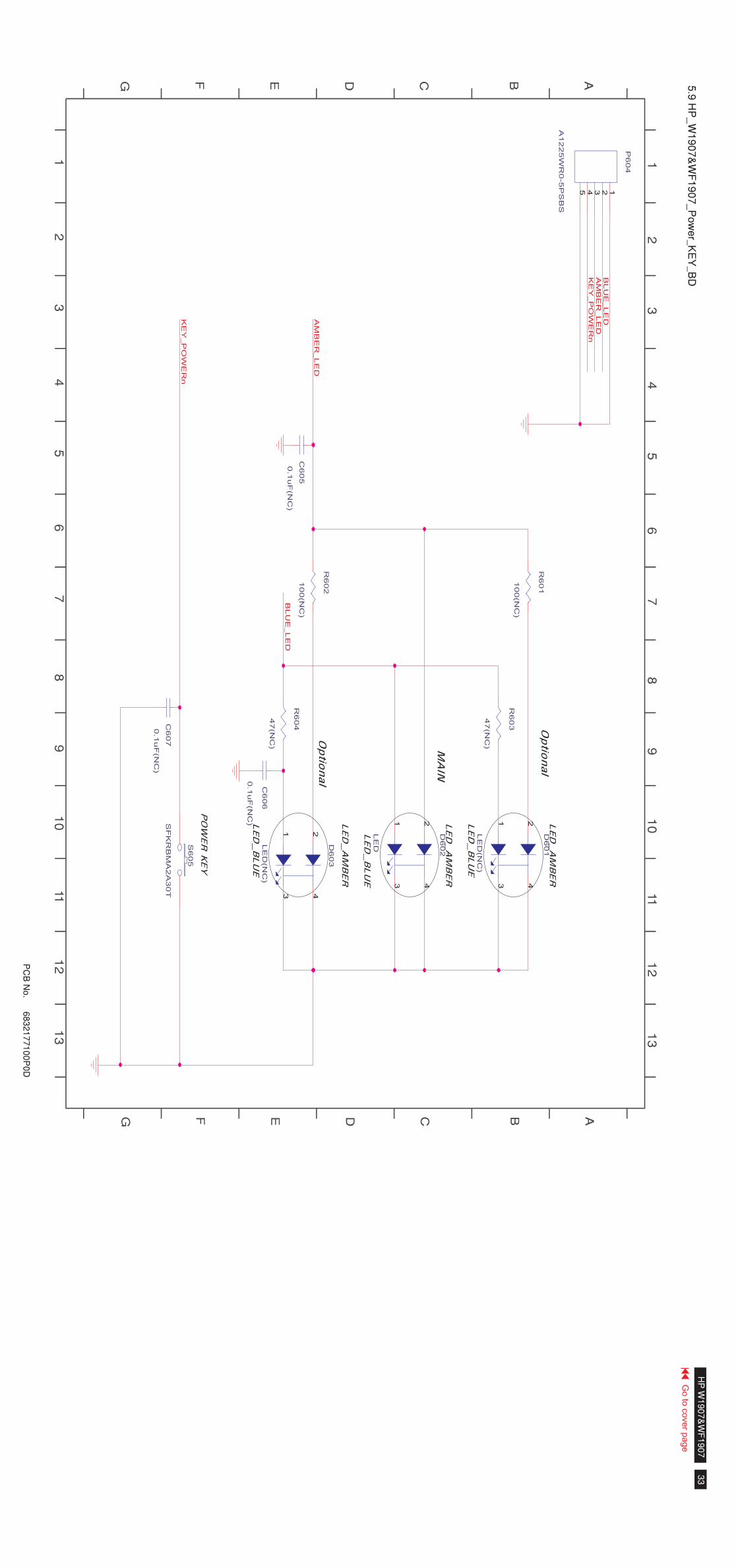
.5
9H
P_
W1
90
7&
WF
19
07
_P
ow
er
KE
YB
D_
_
PC
BN
o.
68
32
17
71
00
P0
D
LED
AMBER
_
LED
AMBER
_
LED
BLUE
_
LED
AMBER
_
LED
BLUE
_
LED
BLUE
_
POWERKEY
MAIN
Optional
Optional
AM
BE
RL
ED
_K
EY
PO
WE
Rn
_
BL
UE
LE
D_
KE
YP
OW
ER
n_
AM
BE
RL
ED
_
BL
UE
LE
D_
D6
02
LE
D
13
24
R6
04
47
NC
()
C6
05
01
uF
NC
.(
)
C6
06
01
uF
NC
.(
)
P6
04
A1
22
5W
R0
5P
SB
S-
12345
D6
01
LE
DN
C(
)
13
24
R6
03
47
NC
()
S6
05
SF
KR
BM
A2
A3
0T
R6
01
10
0N
C(
)
R6
02
10
0N
C(
)
D6
03
LE
DN
C(
)
13
24
C6
07
01
uF
NC
.(
)
33
Go
tocover
page
HP
W1
90
7&
WF
19
07
12
34
56
78
91
011
12
13
12
34
56
78
91
011
12
13
ABCDEFG
ABCDEFG