Mechanics and Tribology of MEMS Materials -...
83
SANDIA REPORT SAND20041319 Unlimited Release Printed April 2004 Mechanics and Tribology of MEMS Materials M.T. Dugger, B.L. Boyce, T.E. Buchheit and S.V. Prasad Prepared by Sandia National Laboratories Albuquerque, New Mexico 87185 and Livermore, California 94550 Sandia is a multiprogram laboratory operated by Sandia Corporation, a Lockheed Martin Company, for the United States Department of Energy under Contract DE-AC04-94AL85000. Approved for public release; further dissemination unlimited.
Transcript of Mechanics and Tribology of MEMS Materials -...
SANDIA REPORT SAND2004�1319 Unlimited Release Printed April 2004
Mechanics and Tribology of MEMS Materials M.T. Dugger, B.L. Boyce, T.E. Buchheit and S.V. Prasad
Prepared by Sandia National Laboratories Albuquerque, New Mexico 87185 and Livermore, California 94550
Sandia is a multiprogram laboratory operated by Sandia Corporation, a Lockheed Martin Company, for the United States Department of Energy under Contract DE-AC04-94AL85000. Approved for public release; further dissemination unlimited.
2
Issued by Sandia National Laboratories, operated for the United States Department of Energy by Sandia Corporation. NOTICE: This report was prepared as an account of work sponsored by an agency of the United States Government. Neither the United States Govern-ment nor any agency thereof, nor any of their employees, nor any of their contractors, subcontractors, or their employees, makes any warranty,express or implied, or assumes any legal liability or responsibility for the accuracy, completeness, or usefulness of any information, apparatus, product, or process disclosed, or represents that its use would not infringe privately owned rights. Reference herein to any specific commercial product, process, or service by trade name, trademark, manufacturer, or otherwise, does not necessarily constitute or imply its endorsement, recommendation,or favoring by the United States Government, any agency thereof, or any of their contractors or subcontractors. The views and opinions expressedherein do not necessarily state or reflect those of the United States Govern-ment, any agency thereof, or any of their contractors. Printed in the United States of America. This report has been reproduced directly from the best available copy. Available to DOE and DOE contractors from
U.S. Department of Energy Office of Scientific and Technical Information P.O. Box 62 Oak Ridge, TN 37831 Telephone: (865)576-8401 Facsimile: (865)576-5728 E-Mail: [email protected] Online ordering: http://www.doe.gov/bridge
Available to the public from
U.S. Department of Commerce National Technical Information Service 5285 Port Royal Rd Springfield, VA 22161 Telephone: (800)553-6847 Facsimile: (703)605-6900 E-Mail: [email protected]
Online order: http://www.ntis.gov/ordering.htm
3
SAND2004-1319 Unlimited Release Printed April 2004
Mechanics and Tribology of MEMS Materials
Michael T. Dugger, Brad L. Boyce, Thomas E. Buchheit, and Somuri V. Prasad
Microsystem Materials, Tribology and Technology Department
Sandia National Laboratories P.O. Box 5800
Albuquerque, NM 87185-0889
Abstract Micromachines have the potential to significantly impact future weapon component
designs as well as other defense, industrial, and consumer product applications. For both electroplated (LIGA) and surface micromachined (SMM) structural elements, the influence of processing on structure, and the resultant effects on material properties are not well understood. The behavior of dynamic interfaces in present as-fabricated microsystem materials is inadequate for most applications and the fundamental relationships between processing conditions and tribological behavior in these systems are not clearly defined. We intend to develop a basic understanding of deformation, fracture, and surface interactions responsible for friction and wear of microelectromechanical system (MEMS) materials. This will enable needed design flexibility for these devices, as well as strengthen our understanding of material behavior at the nanoscale. The goal of this project is to develop new capabilities for sub-microscale mechanical and tribological measurements, and to exercise these capabilities to investigate material behavior at this size scale.

4
Acknowledgements The authors thank the management of Research Foundations programs in Center 1800 for
supporting the development of the friction measurement infrastructure used in this project. We also thank the personnel of the Microelectronics Development Laboratory for fabricating the MEMS structures used in this work. Finally, we thank the LDRD program office for the opportunity to explore the mechanical behavior, friction and wear behavior of materials for microsystem applications.
5
Contents
ACKNOWLEDGEMENTS..............................................................................................4
PREFACE ....................................................................................................................13
1 DEVELOPMENT OF IMPROVED MECHANICAL TEST CAPABILITIES FOR SMM MATERIALS ................................................................................................................14
1.1 Background on MEMS Strength Evaluation ..............................................................14
1.2 Improvement of MEMS Tensile Strength Evaluation Methodology ........................15
1.3 Development of a MEMS Mechanical Probe Station .................................................18
1.4 Development of next-generation SMM mechanical test structures and on-chip force/displacement sensors........................................................................................................19
1.4.1 Pull-tab tensile specimens........................................................................................20 1.4.2 Fracture-toughness structures. .................................................................................21 1.4.3 Bend strength structures...........................................................................................22 1.4.4 Optical force transducer...........................................................................................22
1.5 References.......................................................................................................................23
2 STRENGTH DISTRIBUTIONS IN SUMMITTM SMM POLYSILICON....................25
2.1 Weibull Analysis of Strength Distributions in SUMMiTTM Polysilicon ...................25
2.2 Critical Flaw Size Evaluation .......................................................................................27
2.3 Size-Dependence in Polysilicon Strength.....................................................................28
2.4 Layer Dependence on Strength.....................................................................................30
2.5 References.......................................................................................................................32
3 THE ROLE OF MICROSTRUCTURE IN SUMMITTM POLYSILICON FAILURE ..33
3.1 Characterization of Polysilicon Microstructure .........................................................33
3.2 Simulating the Response of Polycrystalline Silicon ....................................................34 3.2.1 Simulation Procedure...............................................................................................34 3.2.2 Results and Discussion ............................................................................................35
6
3.3 Summary.........................................................................................................................38
3.4 References.......................................................................................................................39
4 POWDER-CONSOLIDATED MEMS DEVELOPMENT ........................................40
4.1 Background ....................................................................................................................40
4.2 Method for Evaluating Flexural Strength of Alumina Parts.....................................40
4.3 Results from Flexural Strength Test of Alumina........................................................41
4.4 Method of Evaluating Tensile Behavior of Consolidated Metallic Materials ..........42
4.5 Tensile Behavior of Stainless Steel Parts .....................................................................43
4.6 References.......................................................................................................................45
5 EBSD STUDIES OF WEAR-INDUCED SUBSURFACES IN ELECTROFORMED NICKEL........................................................................................................................46
5.1 Background ....................................................................................................................46
5.2 Introduction....................................................................................................................46
5.3 Experimental ..................................................................................................................47 5.3.1 Specimen preparation ..............................................................................................47 5.3.2 Tribology Testing ....................................................................................................47 5.3.3 Sample Preparation by Focused Ion Beam (FIB) ....................................................47 5.3.4 Electron Backscatter Diffraction Analysis ..............................................................47
5.4 Results and Discussion...................................................................................................48
5.5 Summary and Conclusions ...........................................................................................51
5.6 References.......................................................................................................................52
6 NOVEL TECHNIQUES FOR MEASUREMENT OF ADHESION IN LIGA CONTACTS .................................................................................................................53
6.1 Introduction....................................................................................................................53
6.2 A Review of Analytical Models.....................................................................................54
6.3 Morphology of LIGA Fabricated Structures ..............................................................55
6.4 LIGA Adhesion Probe Tips and Pull-Off Force Measurements ...............................56
7
6.5 Summary.........................................................................................................................57
6.6 References.......................................................................................................................57
7 IMPACT OF SILANE DEGRADATION DUE TO WATER VAPOR AND RADIATION EXPOSURE ON TRIBOLOGICAL BEHAVIOR ......................................59
7.1 ABSTRACT....................................................................................................................59
7.2 INTRODUCTION..........................................................................................................59
7.3 EXPERIMENTAL APPROACH .................................................................................60 7.3.1 Sample types and monolayer deposition .................................................................60 7.3.2 Monolayer characterization .....................................................................................61 7.3.3 Friction measurements .............................................................................................62 7.3.4 Description of radiation exposure facility ...............................................................63 7.3.5 Radiation exposures .................................................................................................63 7.3.6 Dose measurement ...................................................................................................63 7.3.7 Thermal exposures ...................................................................................................64
7.4 RESULTS .......................................................................................................................65 7.4.1 Simulation of dose delivered at GIF ........................................................................65 7.4.2 Simulation of dose delivered during XPS analysis..................................................65 7.4.3 Contact angle ...........................................................................................................67 7.4.4 Chemical analysis ....................................................................................................69 7.4.5 Friction measurements .............................................................................................71
7.5 DISCUSSION .................................................................................................................72
7.6 CONCLUSIONS ............................................................................................................73
7.7 ACKNOWLEDGEMENTS ..........................................................................................73
7.8 REFERENCES...............................................................................................................74
8 FRICTION AND WEAR OF SELECTIVE TUNGSTEN COATINGS FOR SURFACE MICROMACHINED SILICON DEVICES......................................................................75
8.1 Introduction....................................................................................................................75
8.2 Experimental Approach ................................................................................................75 8.2.1 Treatment of SMM devices with selective tungsten................................................75 8.2.2 Surface Chemical Analysis ......................................................................................75 8.2.3 Tribological Measurements of Tungsten-Coated Surfaces......................................76
8.3 Results and Discussion...................................................................................................76

8
8.4 Conclusions.....................................................................................................................80
8.5 References.......................................................................................................................80
9 CONCLUSIONS AND RECOMMENDATIONS.....................................................81
10 DISTRIBUTION.................................................................................................83
9
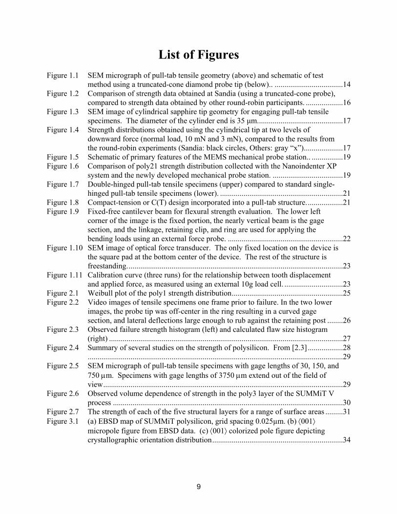
List of Figures Figure 1.1 SEM micrograph of pull-tab tensile geometry (above) and schematic of test
method using a truncated-cone diamond probe tip (below).. ...................................14 Figure 1.2 Comparison of strength data obtained at Sandia (using a truncated-cone probe),
compared to strength data obtained by other round-robin participants. ...................16 Figure 1.3 SEM image of cylindrical sapphire tip geometry for engaging pull-tab tensile
specimens. The diameter of the cylinder end is 35 µm............................................17 Figure 1.4 Strength distributions obtained using the cylindrical tip at two levels of
downward force (normal load, 10 mN and 3 mN), compared to the results from the round-robin experiments (Sandia: black circles, Others: gray �x�)....................17
Figure 1.5 Schematic of primary features of the MEMS mechanical probe station.. ................19 Figure 1.6 Comparison of poly21 strength distribution collected with the Nanoindenter XP
system and the newly developed mechanical probe station. ....................................19 Figure 1.7 Double-hinged pull-tab tensile specimens (upper) compared to standard single-
hinged pull-tab tensile specimens (lower). ...............................................................21 Figure 1.8 Compact-tension or C(T) design incorporated into a pull-tab structure...................21 Figure 1.9 Fixed-free cantilever beam for flexural strength evaluation. The lower left
corner of the image is the fixed portion, the nearly vertical beam is the gage section, and the linkage, retaining clip, and ring are used for applying the bending loads using an external force probe. ...........................................................22
Figure 1.10 SEM image of optical force transducer. The only fixed location on the device is the square pad at the bottom center of the device. The rest of the structure is freestanding...............................................................................................................23
Figure 1.11 Calibration curve (three runs) for the relationship between tooth displacement and applied force, as measured using an external 10g load cell. ..............................23
Figure 2.1 Weibull plot of the poly1 strength distribution.........................................................25 Figure 2.2 Video images of tensile specimens one frame prior to failure. In the two lower
images, the probe tip was off-center in the ring resulting in a curved gage section, and lateral deflections large enough to rub against the retaining post ........26
Figure 2.3 Observed failure strength histogram (left) and calculated flaw size histogram (right) ........................................................................................................................27
Figure 2.4 Summary of several studies on the strength of polysilicon. From [2.3] ..................28 ...................................................................................................................................29 Figure 2.5 SEM micrograph of pull-tab tensile specimens with gage lengths of 30, 150, and
750 µm. Specimens with gage lengths of 3750 µm extend out of the field of view...........................................................................................................................29
Figure 2.6 Observed volume dependence of strength in the poly3 layer of the SUMMiT V process ......................................................................................................................30
Figure 2.7 The strength of each of the five structural layers for a range of surface areas .........31 Figure 3.1 (a) EBSD map of SUMMiT polysilicon, grid spacing 0.025µm. (b) ⟨001⟩
micropole figure from EBSD data. (c) ⟨001⟩ colorized pole figure depicting crystallographic orientation distribution...................................................................34
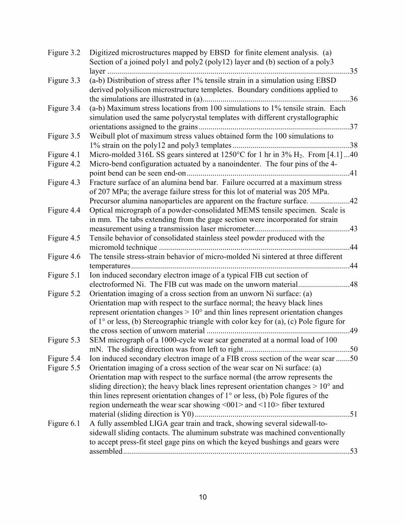
10
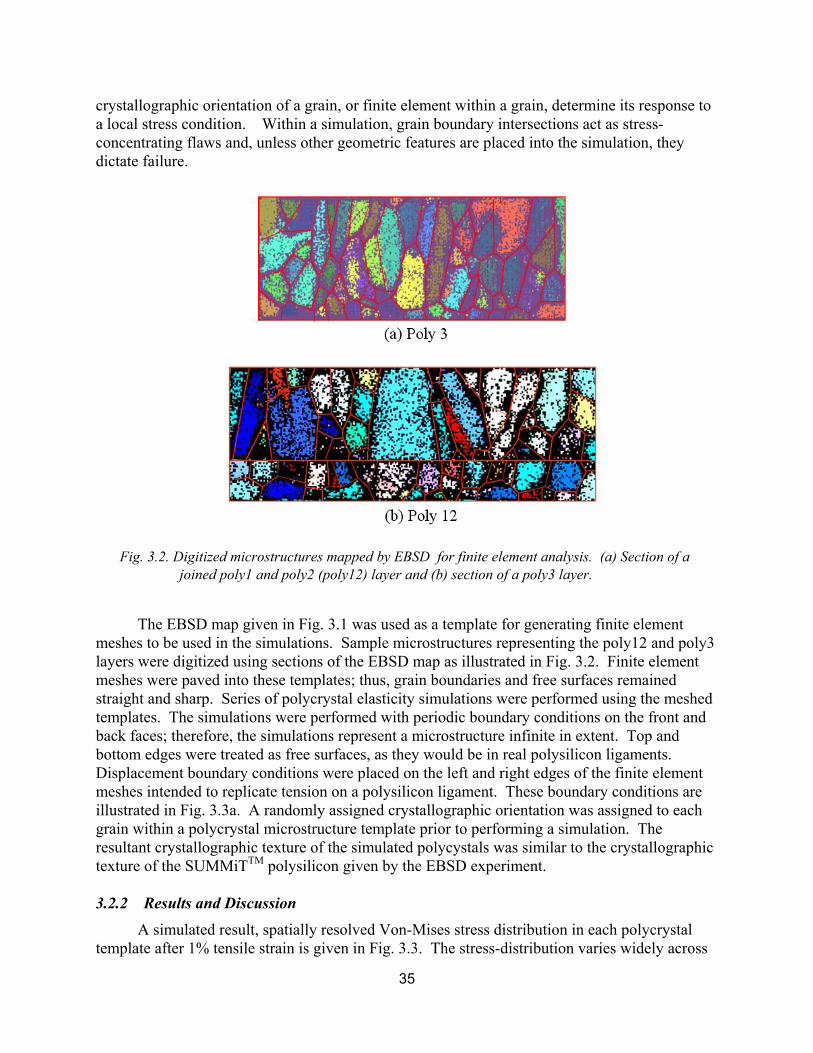
Figure 3.2 Digitized microstructures mapped by EBSD for finite element analysis. (a) Section of a joined poly1 and poly2 (poly12) layer and (b) section of a poly3 layer ..........................................................................................................................35
Figure 3.3 (a-b) Distribution of stress after 1% tensile strain in a simulation using EBSD derived polysilicon microstructure templetes. Boundary conditions applied to the simulations are illustrated in (a)..........................................................................36
Figure 3.4 (a-b) Maximum stress locations from 100 simulations to 1% tensile strain. Each simulation used the same polycrystal templates with different crystallographic orientations assigned to the grains ............................................................................37
Figure 3.5 Weibull plot of maximum stress values obtained form the 100 simulations to 1% strain on the poly12 and poly3 templates ...........................................................38
Figure 4.1 Micro-molded 316L SS gears sintered at 1250°C for 1 hr in 3% H2. From [4.1] ...40 Figure 4.2 Micro-bend configuration actuated by a nanoindenter. The four pins of the 4-
point bend can be seen end-on..................................................................................41 Figure 4.3 Fracture surface of an alumina bend bar. Failure occurred at a maximum stress
of 207 MPa; the average failure stress for this lot of material was 205 MPa. Precursor alumina nanoparticles are apparent on the fracture surface. ....................42
Figure 4.4 Optical micrograph of a powder-consolidated MEMS tensile specimen. Scale is in mm. The tabs extending from the gage section were incorporated for strain measurement using a transmission laser micrometer................................................43
Figure 4.5 Tensile behavior of consolidated stainless steel powder produced with the micromold technique ................................................................................................44
Figure 4.6 The tensile stress-strain behavior of micro-molded Ni sintered at three different temperatures..............................................................................................................44
Figure 5.1 Ion induced secondary electron image of a typical FIB cut section of electroformed Ni. The FIB cut was made on the unworn material..........................48
Figure 5.2 Orientation imaging of a cross section from an unworn Ni surface: (a) Orientation map with respect to the surface normal; the heavy black lines represent orientation changes > 10° and thin lines represent orientation changes of 1° or less, (b) Stereographic triangle with color key for (a), (c) Pole figure for the cross section of unworn material ........................................................................49
Figure 5.3 SEM micrograph of a 1000-cycle wear scar generated at a normal load of 100 mN. The sliding direction was from left to right .....................................................50
Figure 5.4 Ion induced secondary electron image of a FIB cross section of the wear scar .......50 Figure 5.5 Orientation imaging of a cross section of the wear scar on Ni surface: (a)
Orientation map with respect to the surface normal (the arrow represents the sliding direction); the heavy black lines represent orientation changes > 10° and thin lines represent orientation changes of 1° or less, (b) Pole figures of the region underneath the wear scar showing <001> and <110> fiber textured material (sliding direction is Y0) ..............................................................................51
Figure 6.1 A fully assembled LIGA gear train and track, showing several sidewall-to-sidewall sliding contacts. The aluminum substrate was machined conventionally to accept press-fit steel gage pins on which the keyed bushings and gears were assembled..................................................................................................................53
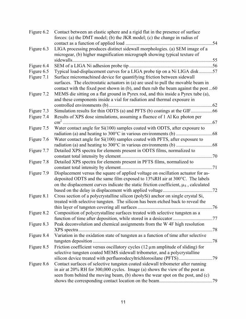
11
Figure 6.2 Contact between an elastic sphere and a rigid flat in the presence of surface forces: (a) the DMT model; (b) the JKR model; (c) the change in radius of contact as a function of applied load ........................................................................54
Figure 6.3 LIGA processing produces distinct sidewall morphologies. (a) SEM image of a microgear, (b) higher magnification micrograph showing typical texture of sidewalls....................................................................................................................55
Figure 6.4 SEM of a LIGA Ni adhesion probe tip .....................................................................56 Figure 6.5 Typical load-displacement curves for a LIGA probe tip on a Ni LIGA disk ...........57 Figure 7.1 Surface micromachined device for quantifying friction between sidewall
surfaces. The electrostatic actuators in (a) are used to pull the movable beam in contact with the fixed post shown in (b), and then rub the beam against the post ...60
Figure 7.2 MEMS die sitting on a flat ground in Pyrex rod, and this inside a Pyrex tube (a), and these components inside a vial for radiation and thermal exposure in controlled environments (b)......................................................................................62
Figure 7.3 Simulation results for thin ODTS (a) and PFTS (b) coatings at the GIF..................66 Figure 7.4 Results of XPS dose simulations, assuming a fluence of 1 Al Kα photon per
cm2 ............................................................................................................................67 Figure 7.5 Water contact angle for Si(100) samples coated with ODTS, after exposure to
radiation (a) and heating to 300°C in various environments (b) ..............................68 Figure 7.6 Water contact angle for Si(100) samples coated with PFTS, after exposure to
radiation (a) and heating to 300°C in various environments (b) ..............................68 Figure 7.7 Detailed XPS spectra for elements present in ODTS films, normalized to
constant total intensity by element............................................................................70 Figure 7.8 Detailed XPS spectra for elements present in PFTS films, normalized to
constant total intensity by element............................................................................71 Figure 7.9 Displacement versus the square of applied voltage on oscillation actuator for as-
deposited ODTS and the same film exposed to 13%RH air at 300°C. The labels on the displacement curves indicate the static friction coefficient, µS , calculated based on the delay in displacement with applied voltage.........................................72
Figure 8.1 Cross section of a polycrystalline silicon (polySi) anchor on single crystal Si, treated with selective tungsten. The silicon has been etched back to reveal the thin layer of tungsten covering all surfaces ..............................................................76
Figure 8.2 Composition of polycrystalline surfaces treated with selective tungsten as a function of time after deposition, while stored in a desiccator.................................77
Figure 8.3 Peak deconvolution and chemical assignments from the W 4F high resolution XPS spectra...............................................................................................................78
Figure 8.4 Variation in the oxidation state of tungsten as a function of time after selective tungsten deposition ...................................................................................................78
Figure 8.5 Friction coefficient versus oscillatory cycles (12 µm amplitude of sliding) for selective tungsten coated MEMS sidewall tribometer, and a polycrystalline silicon device treated with perfluorodecyltrichlorosilane (PFTS)............................79
Figure 8.6 Contact surfaces of selective tungsten coated sidewall tribometer after running in air at 20% RH for 300,000 cycles. Image (a) shows the view of the post as seen from behind the moving beam, (b) shows the wear spot on the post, and (c) shows the corresponding contact location on the beam............................................79
12
List of Tables
Table 2.1 Observed Weibull modulus, m, and bounds based on one standard deviation (1SD), as inferred from the volumetric dependence of strength ................................30
Table 7.1 Matrix of samples for radiation exposures at GIF......................................................63 Table 7.2 Matrix of samples for thermal exposures ...................................................................64 Table 7.3 Composition of alkylsilane coatings for ADEPT simulations ...................................65 Table 7.4 Atomic concentration of species as a function of exposure conditions for ODTS
coated Si(100).............................................................................................................69 Table 7.5 Atomic concentration of species as a function of exposure conditions for PFTS
coated Si(100).............................................................................................................70

13
Preface Our team was involved in a three-year LDRD investigation of mechanical and tribological
behavior of materials for microelectromechanical systems (MEMS). The overall goals of this work were a) to develop test samples and methodologies to probe the behavior of materials at the size scale of MEMS components, b) to evaluate the performance and failure modes of MEMS materials, and c) to develop simulation tools to predict the behavior of materials during deformation.
This report will document all of the significant findings made during the investigation. This report is divided into nine chapters as follows: • Chapter 1 covers development of mechanical test capabilities for MEMS materials. • Chapter 2 gives the results of an investigation of strength distributions in polycrystalline
silicon, and comparison of test techniques to other results during round robin testing. • Chapter 3 discusses the role of microstructure in fracture of polycrystalline, and
development of simulation tools for polycrystal plasticity. • Chapter 4 covers development of powder-consolidated LIGA components, and strength
measurements of these materials. • Chapter 5 deals with studies of the evolution in subsurface damage during sliding contact
with polycrystalline nickel films created in the LIGA process. • Chapter 6 discusses the degradation of alkylsilane films during exposure to water vapor and
elevated temperatures, and radiation environments, and the impact of changes in the monolayer on the friction behavior of MEMS contacts.
• Chapter 7 presents the results of a study of radiative and thermal degradation of alkylsilane monolayers for silicon surface micromachines in environments relevant to Sandia mission applications and back-end-of-line processing.
• Chapter 8 shows the results of an examination of selective tungsten coating processes to improve the wear resistance of surface micromachined devices.
• Chapter 9 contains conclusions and recommendations from the work.
14
1 Development of Improved Mechanical Test Capabilities for SMM Materials
1.1 Background on MEMS Strength Evaluation
Evaluation of the tensile strength of polysilicon is motivated by the notion that nearly all MEMS applications involve significant component stresses, and the proximity of such stresses to fundamental material limits must be established, preferably with a statistical certainty for safety-critical applications. Moreover, a study on the strength limits of these MEMS materials can provide insight into the origin of failure-critical flaws, thereby guiding improvements in processing that lead to improved mechanical performance.
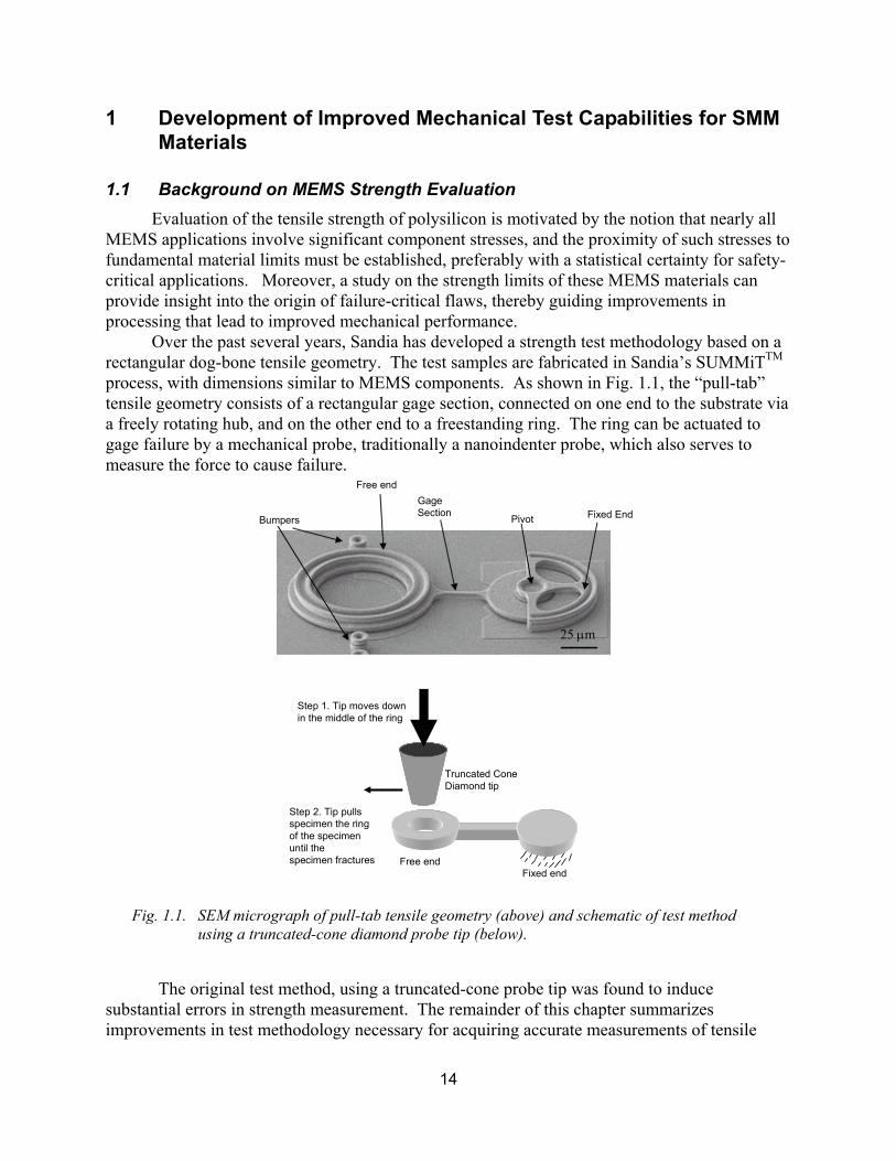
Over the past several years, Sandia has developed a strength test methodology based on a rectangular dog-bone tensile geometry. The test samples are fabricated in Sandia�s SUMMiTTM process, with dimensions similar to MEMS components. As shown in Fig. 1.1, the �pull-tab� tensile geometry consists of a rectangular gage section, connected on one end to the substrate via a freely rotating hub, and on the other end to a freestanding ring. The ring can be actuated to gage failure by a mechanical probe, traditionally a nanoindenter probe, which also serves to measure the force to cause failure.
Free endFixed end
Truncated Cone Diamond tip
Step 1. Tip moves down in the middle of the ring
Step 2. Tip pullsspecimen the ring of the specimen until the specimen fractures
25 µm
Fixed EndPivot
Free end
Bumpers
Gage Section
Fig. 1.1. SEM micrograph of pull-tab tensile geometry (above) and schematic of test method
using a truncated-cone diamond probe tip (below).
The original test method, using a truncated-cone probe tip was found to induce substantial errors in strength measurement. The remainder of this chapter summarizes improvements in test methodology necessary for acquiring accurate measurements of tensile
15
strength. The subsequent chapter discusses the observed strength behavior, using this improved test methodology.
1.2 Improvement of MEMS Tensile Strength Evaluation Methodology
Several testing techniques have been published with widely varying tensile strengths appearing in the literature - between 1 to 4 GPa [1.1-1.6]. Much of the variation between authors has been explained in terms of microstructural differences due to deposition conditions, sample size effects and release processing. A previous cross comparison exercise involving direct and indirect testing techniques using the same material, but different releases techniques, reported significant variations [1.7].
Tensile data was collected from five investigators that employed two essentially different types of samples, with further variations in size within each group. The larger sized group of samples were designed to be gripped with an electrostatic force applied to the enlarged end of a sample, the tensile force application and measurement were performed with a macro scale system; slightly different versions of this system were used by Tsuchiya [1.8], and Sharpe and Coles [1.9]. Chasiotis and Knauss also tested this size sample, but used the electrostatic force only to assist in the adhesive bonding of the sample to the grip [1.10]. Samples of four sizes were tested by these three labs, with widths of 6 and 20 µm and lengths of 250 and 1000 mm. The second sample type, tested by Read [1.11], and by LaVan at Sandia [1.12], is 1.8 µm wide and 15 to 1000 µm long.
All of the samples were produced using Sandia National Labs SUMMiTTM IV polysilicon process � they were patterned in the poly1-2 composite layer that is 2.5 mm thick. Samples of all sizes were produced side by side on the same die, five or more die were sent to each participant. The films were deposited as n-type, fine grained polysilicon from silane in a low pressure chemical vapor deposition (LPCVD) furnace at ~580°C. The intervening sacrificial oxide layers were also deposited in an LPCVD furnace from tetraethylorthosilicate (TEOS) at ~720°C. This process usually uses 6-inch, (100) n-type silicon wafers of 2 to 20 ohm/cm resistivity covered by 6000 Å of thermal oxide followed by 8000 Å of LPCVD silicon nitride for electrical isolation. Thickness was accurately controlled during the deposition process and was measured, along with width, in a calibrated SEM after release (accuracy 0.1 µm). The samples were released, coated with a self-assembling monolayer (SAM) such as octadecyltrichlorosilane (ODTS) or perfluorodecyltrichloro-silane (FDTS) as an anti-stiction coating and then dried with super-critical CO2. The microstructure and crystallographic texture of this polysilicon have been well characterized. The texture is random. The grain morphology is columnar, with a mean column diameter of 300-400 nm. Most of the grains bridge from the top to bottom surface of the film. More details of the process may be found in [1.13].
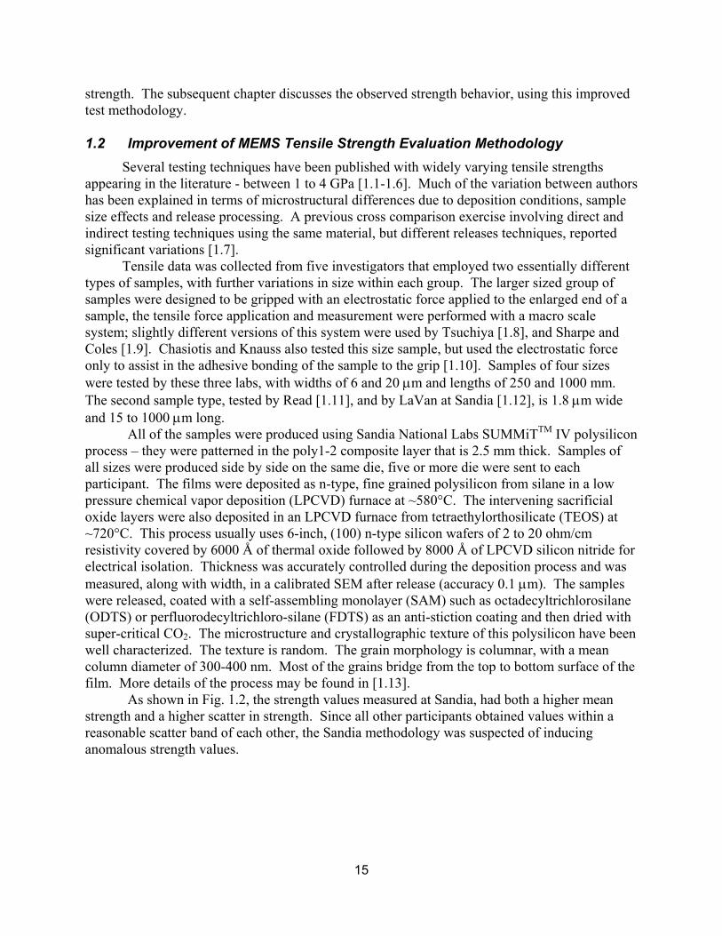
As shown in Fig. 1.2, the strength values measured at Sandia, had both a higher mean strength and a higher scatter in strength. Since all other participants obtained values within a reasonable scatter band of each other, the Sandia methodology was suspected of inducing anomalous strength values.
16
1
2
3
4
5
6
0 0.2 0.4 0.6 0.8 1
Frac
ture
Stre
ngth
(GP
a)
Probability
Sandia
Other Round-Robin Participants:Toyota, Johns Hopkins, Cal Tech
Poly 21, Reticule Set 184
Fig. 1.2. Comparison of strength data obtained at Sandia (using a truncated-cone probe), compared to strength data obtained by other round-robin participants. Based on [8].
One of the primary distinctions between the Sandia method and all other methods was the use of a truncated cylinder to engage the ring-end of the pull-tab specimen. This tip geometry required that a significant downward force, ~400 mN, be applied to the substrate to prevent the conical tip from sliding over the engagement ring rather than pulling the ring to failure. This downward force was over an order of magnitude higher than the observed lateral forces associated with silicon failure. While corrections were made to adjust for the contributions of sliding friction and the resultant force vector resolved in the direction of the gage length, this conical engagement geometry remained suspect.
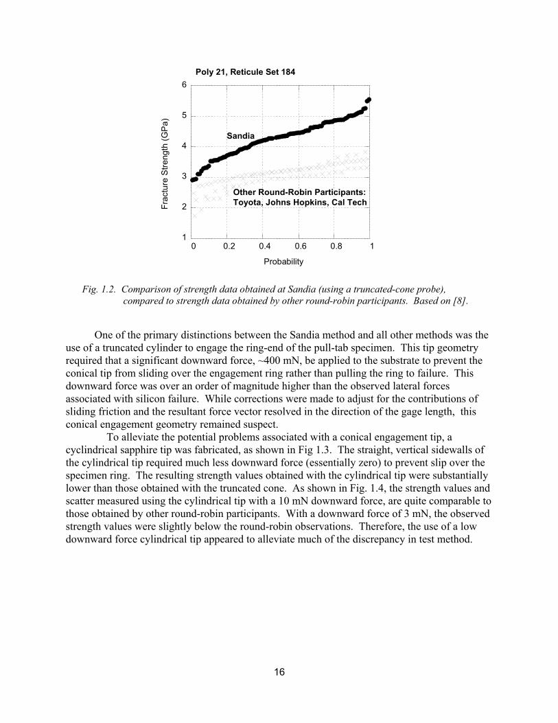
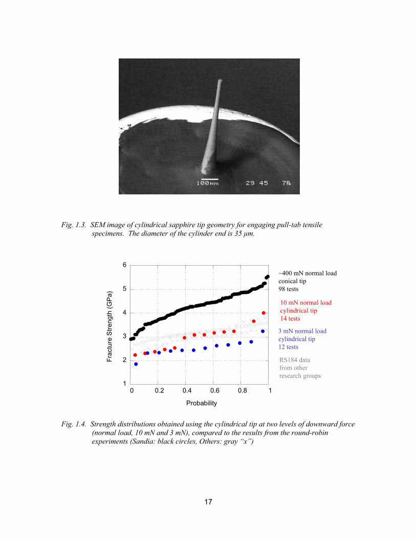
To alleviate the potential problems associated with a conical engagement tip, a cyclindrical sapphire tip was fabricated, as shown in Fig 1.3. The straight, vertical sidewalls of the cylindrical tip required much less downward force (essentially zero) to prevent slip over the specimen ring. The resulting strength values obtained with the cylindrical tip were substantially lower than those obtained with the truncated cone. As shown in Fig. 1.4, the strength values and scatter measured using the cylindrical tip with a 10 mN downward force, are quite comparable to those obtained by other round-robin participants. With a downward force of 3 mN, the observed strength values were slightly below the round-robin observations. Therefore, the use of a low downward force cylindrical tip appeared to alleviate much of the discrepancy in test method.
17
Fig. 1.3. SEM image of cylindrical sapphire tip geometry for engaging pull-tab tensile specimens. The diameter of the cylinder end is 35 µm.
Fig. 1.4. Strength distributions obtained using the cylindrical tip at two levels of downward force
(normal load, 10 mN and 3 mN), compared to the results from the round-robin experiments (Sandia: black circles, Others: gray �x�)
~400 mN normal loadconical tip98 tests
10 mN normal loadcylindrical tip14 tests
3 mN normal loadcylindrical tip12 tests
RS184 data from other research groups
1
2
3
4
5
6
0 0.2 0.4 0.6 0.8 1
Frac
ture
Stre
ngth
(GP
a)
Probability
18
1.3 Development of a MEMS Mechanical Probe Station All early testing of the MEMS pull-tab tensile geometry utilized the lateral force
capability of an MTS Nanoindenter XP. While the lateral force capability provided adequate force resolution (~10 µN), the Nanoindenter approach had several drawbacks: (a) during the experiments, optics could not be used to observe behavior, (b) electrical contacts could not be made using probe tips, (c) the XP instrument was in high demand for nanoindentation, its intended purpose, (d) the cost of this instrument (~$200K) prohibited this technique from being adopted by other research groups. To overcome these issues, a mechanical probe station was developed. The objective of the development was to provide an open, flexible platform capable of testing MEMS devices with similar or better force resolution, while addressing the aforementioned limitations.
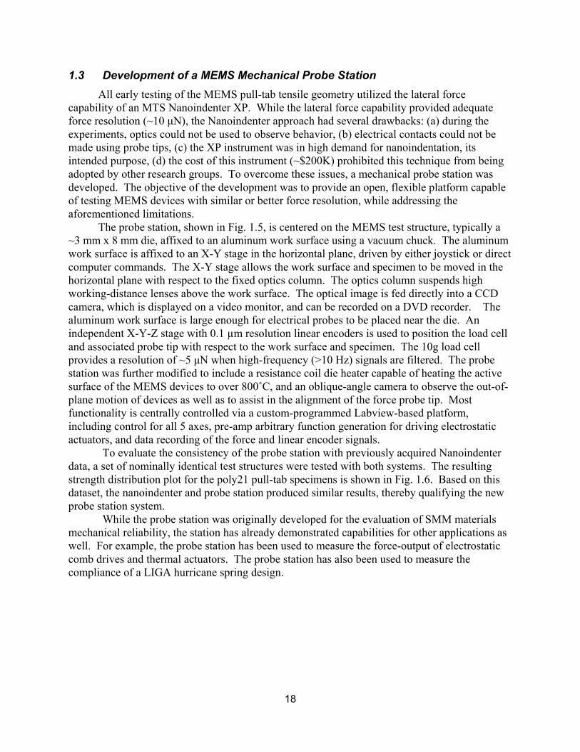
The probe station, shown in Fig. 1.5, is centered on the MEMS test structure, typically a ~3 mm x 8 mm die, affixed to an aluminum work surface using a vacuum chuck. The aluminum work surface is affixed to an X-Y stage in the horizontal plane, driven by either joystick or direct computer commands. The X-Y stage allows the work surface and specimen to be moved in the horizontal plane with respect to the fixed optics column. The optics column suspends high working-distance lenses above the work surface. The optical image is fed directly into a CCD camera, which is displayed on a video monitor, and can be recorded on a DVD recorder. The aluminum work surface is large enough for electrical probes to be placed near the die. An independent X-Y-Z stage with 0.1 µm resolution linear encoders is used to position the load cell and associated probe tip with respect to the work surface and specimen. The 10g load cell provides a resolution of ~5 µN when high-frequency (>10 Hz) signals are filtered. The probe station was further modified to include a resistance coil die heater capable of heating the active surface of the MEMS devices to over 800ûC, and an oblique-angle camera to observe the out-of-plane motion of devices as well as to assist in the alignment of the force probe tip. Most functionality is centrally controlled via a custom-programmed Labview-based platform, including control for all 5 axes, pre-amp arbitrary function generation for driving electrostatic actuators, and data recording of the force and linear encoder signals.
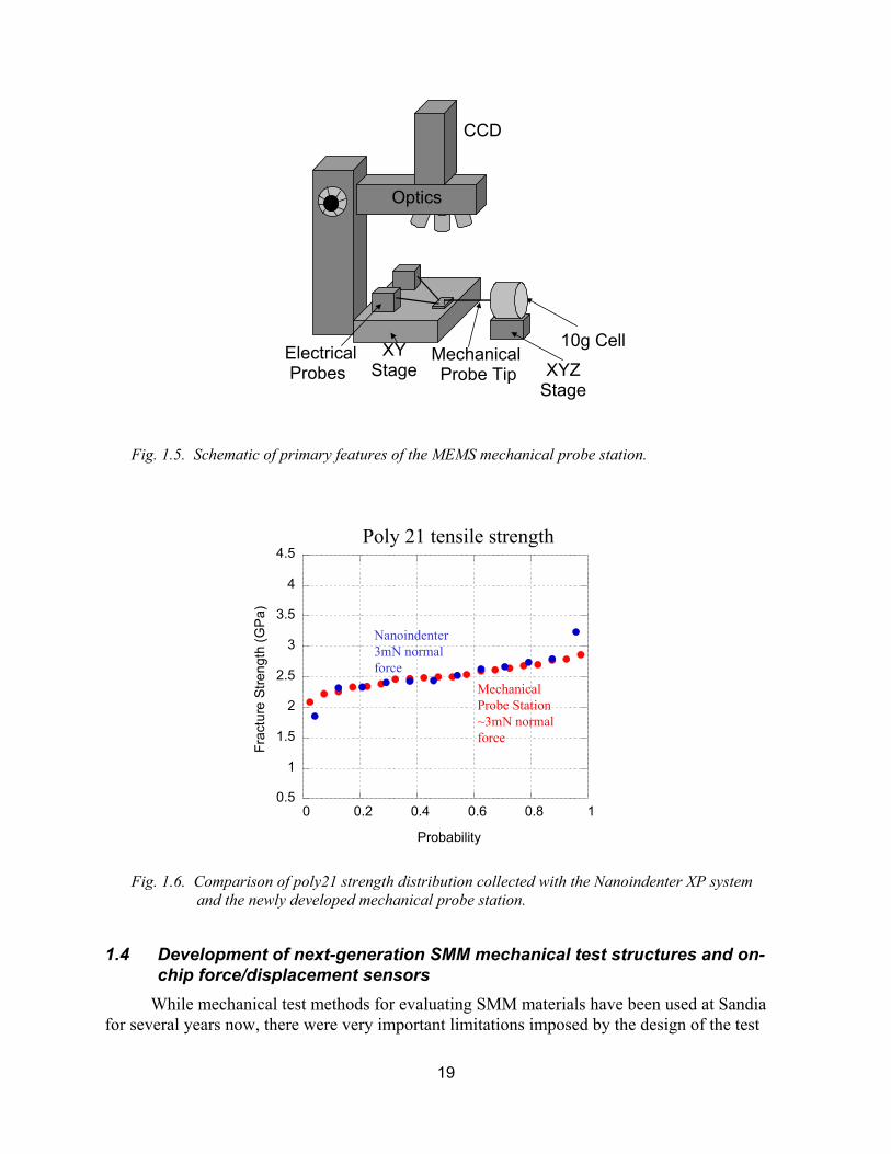
To evaluate the consistency of the probe station with previously acquired Nanoindenter data, a set of nominally identical test structures were tested with both systems. The resulting strength distribution plot for the poly21 pull-tab specimens is shown in Fig. 1.6. Based on this dataset, the nanoindenter and probe station produced similar results, thereby qualifying the new probe station system.
While the probe station was originally developed for the evaluation of SMM materials mechanical reliability, the station has already demonstrated capabilities for other applications as well. For example, the probe station has been used to measure the force-output of electrostatic comb drives and thermal actuators. The probe station has also been used to measure the compliance of a LIGA hurricane spring design.
19
Fig. 1.5. Schematic of primary features of the MEMS mechanical probe station.
Fig. 1.6. Comparison of poly21 strength distribution collected with the Nanoindenter XP system
and the newly developed mechanical probe station.
1.4 Development of next-generation SMM mechanical test structures and on-chip force/displacement sensors
While mechanical test methods for evaluating SMM materials have been used at Sandia for several years now, there were very important limitations imposed by the design of the test
Optics
CCD
XY Stage
10g CellElectrical Probes
Mechanical Probe Tip XYZ
Stage
0.5
1
1.5
2
2.5
3
3.5
4
4.5
0 0.2 0.4 0.6 0.8 1
Frac
ture
Stre
ngth
(GP
a)
Probability
Poly 21 tensile strength
Mechanical Probe Station~3mN normal force
Nanoindenter 3mN normal force
20
structures. The pull-tab tensile specimen only allowed the evaluation of tensile strength (and with an artificially-induced crack, the evaluation of fracture toughness). Design imperfections in the test structure prohibited the evaluation of the poly3 and poly4 structural layers. Therefore, a set of next-generation test structures were developed to permit the evaluation of a wider range of mechanical properties (bend strength, fracture toughness via the compact-tension geometry, fatigue) as well as to evaluate improvements in the pull-tab design.
Another limitation of the current test methodology is the need for an external force sensor and the lack of any strain measurement. For this reason, several potential designs for on-chip force and displacement sensing were designed and evaluated.
1.4.1 Pull-tab tensile specimens
Early pull-tab tensile specimens almost invariably failed at the fillet which transitioned from the gage section to the hub or ring. To study this, four different fillet radii were evaluated: 8 µm, 15 µm, 25 µm, and 40 µm. The 8 and 15 µm radius specimens always exhibited failure in the fillet region, whereas the 25 and 40 mm specimens sometimes failed in the gage section, and other times in the fillet region. Subsequent designs have always incorporated fillet radii of at least 25 mm. Regardless of the fillet radii, often the gage section would fail in multiple locations, leading to the ejection and loss of gage fragments. This is thought to be due to the large elastic energy stored prior to initial failure, and the interaction of the propagating elastic release shock wave through the gage section. Multiple failure events prevent the identification of the original failure surface, and hence the original flaw. An hour-glass tensile geometry will be evaluated in a future design in an attempt to force single location failure.
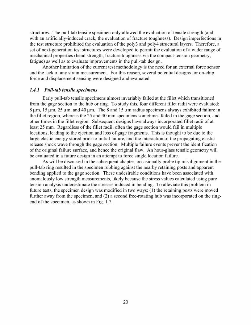
As will be discussed in the subsequent chapter, occasionally probe tip misalignment in the pull-tab ring resulted in the specimen rubbing against the nearby retaining posts and apparent bending applied to the gage section. These undesirable conditions have been associated with anomalously low strength measurements, likely because the stress values calculated using pure tension analysis underestimate the stresses induced in bending. To alleviate this problem in future tests, the specimen design was modified in two ways: (1) the retaining posts were moved further away from the specimen, and (2) a second free-rotating hub was incorporated on the ring-end of the specimen, as shown in Fig. 1.7.
21
Fig 1.7 Double-hinged pull-tab tensile specimens (upper) compared to standard single-hinged
pull-tab tensile specimens (lower).
1.4.2 Fracture-toughness structures.
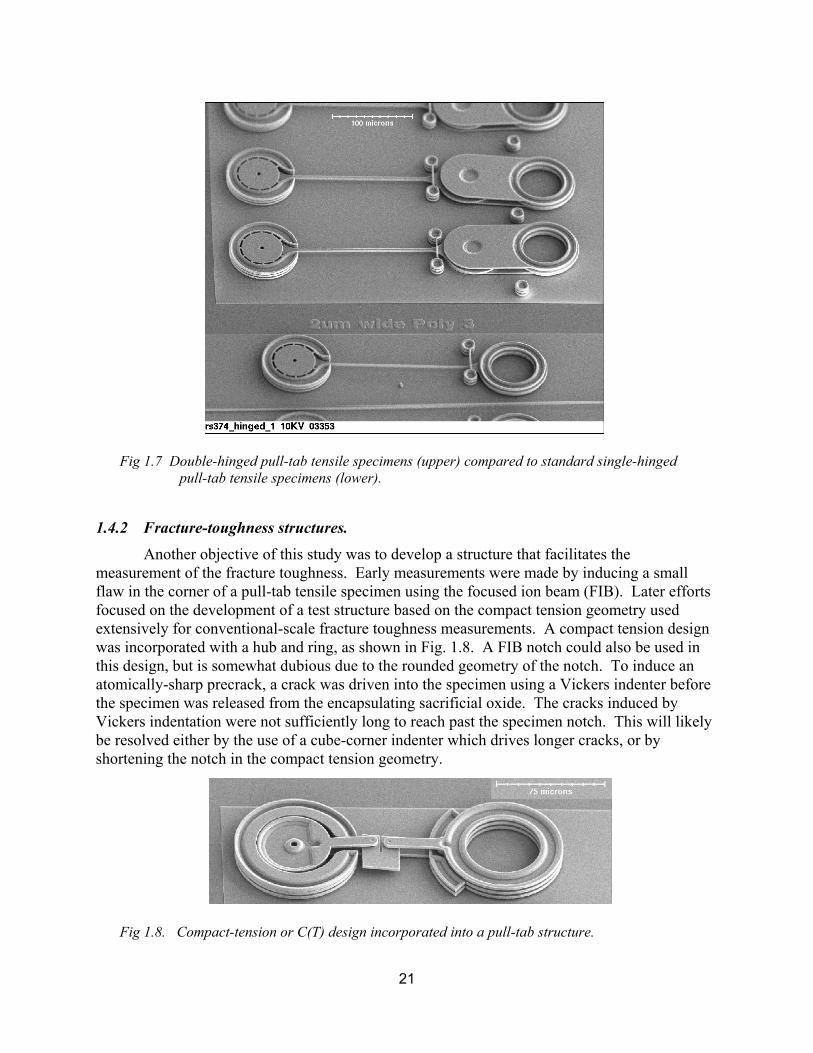
Another objective of this study was to develop a structure that facilitates the measurement of the fracture toughness. Early measurements were made by inducing a small flaw in the corner of a pull-tab tensile specimen using the focused ion beam (FIB). Later efforts focused on the development of a test structure based on the compact tension geometry used extensively for conventional-scale fracture toughness measurements. A compact tension design was incorporated with a hub and ring, as shown in Fig. 1.8. A FIB notch could also be used in this design, but is somewhat dubious due to the rounded geometry of the notch. To induce an atomically-sharp precrack, a crack was driven into the specimen using a Vickers indenter before the specimen was released from the encapsulating sacrificial oxide. The cracks induced by Vickers indentation were not sufficiently long to reach past the specimen notch. This will likely be resolved either by the use of a cube-corner indenter which drives longer cracks, or by shortening the notch in the compact tension geometry.
Fig 1.8. Compact-tension or C(T) design incorporated into a pull-tab structure.
22
1.4.3 Bend strength structures.
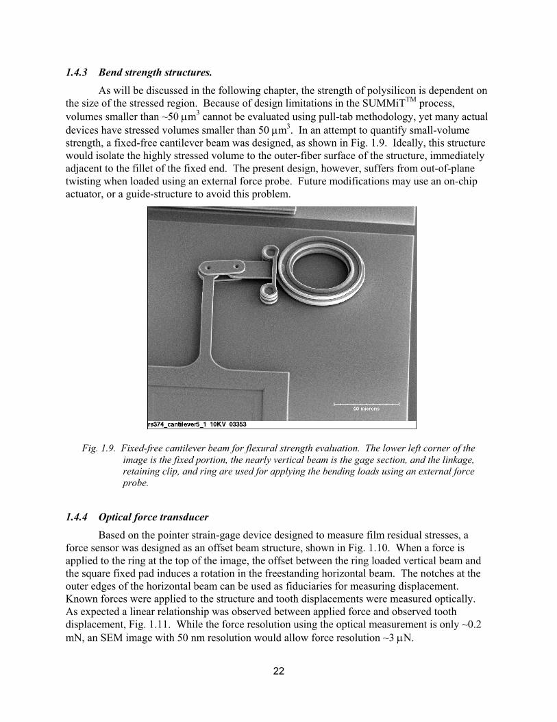
As will be discussed in the following chapter, the strength of polysilicon is dependent on the size of the stressed region. Because of design limitations in the SUMMiTTM process, volumes smaller than ~50 µm3 cannot be evaluated using pull-tab methodology, yet many actual devices have stressed volumes smaller than 50 µm3. In an attempt to quantify small-volume strength, a fixed-free cantilever beam was designed, as shown in Fig. 1.9. Ideally, this structure would isolate the highly stressed volume to the outer-fiber surface of the structure, immediately adjacent to the fillet of the fixed end. The present design, however, suffers from out-of-plane twisting when loaded using an external force probe. Future modifications may use an on-chip actuator, or a guide-structure to avoid this problem.
Fig. 1.9. Fixed-free cantilever beam for flexural strength evaluation. The lower left corner of the
image is the fixed portion, the nearly vertical beam is the gage section, and the linkage, retaining clip, and ring are used for applying the bending loads using an external force probe.
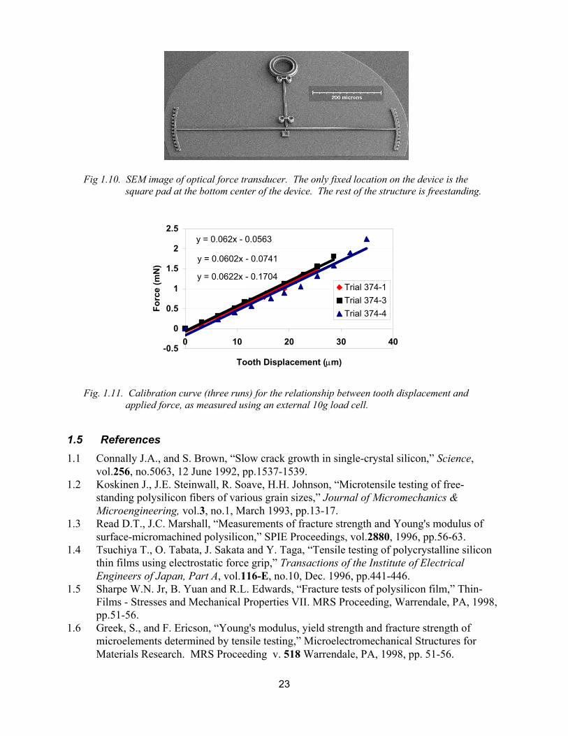
1.4.4 Optical force transducer
Based on the pointer strain-gage device designed to measure film residual stresses, a force sensor was designed as an offset beam structure, shown in Fig. 1.10. When a force is applied to the ring at the top of the image, the offset between the ring loaded vertical beam and the square fixed pad induces a rotation in the freestanding horizontal beam. The notches at the outer edges of the horizontal beam can be used as fiduciaries for measuring displacement. Known forces were applied to the structure and tooth displacements were measured optically. As expected a linear relationship was observed between applied force and observed tooth displacement, Fig. 1.11. While the force resolution using the optical measurement is only ~0.2 mN, an SEM image with 50 nm resolution would allow force resolution ~3 µN.
23
Fig 1.10. SEM image of optical force transducer. The only fixed location on the device is the
square pad at the bottom center of the device. The rest of the structure is freestanding.
Fig. 1.11. Calibration curve (three runs) for the relationship between tooth displacement and
applied force, as measured using an external 10g load cell.
1.5 References 1.1 Connally J.A., and S. Brown, �Slow crack growth in single-crystal silicon,� Science,
vol.256, no.5063, 12 June 1992, pp.1537-1539. 1.2 Koskinen J., J.E. Steinwall, R. Soave, H.H. Johnson, �Microtensile testing of free-
standing polysilicon fibers of various grain sizes,� Journal of Micromechanics & Microengineering, vol.3, no.1, March 1993, pp.13-17.
1.3 Read D.T., J.C. Marshall, �Measurements of fracture strength and Young's modulus of surface-micromachined polysilicon,� SPIE Proceedings, vol.2880, 1996, pp.56-63.
1.4 Tsuchiya T., O. Tabata, J. Sakata and Y. Taga, �Tensile testing of polycrystalline silicon thin films using electrostatic force grip,� Transactions of the Institute of Electrical Engineers of Japan, Part A, vol.116-E, no.10, Dec. 1996, pp.441-446.
1.5 Sharpe W.N. Jr, B. Yuan and R.L. Edwards, �Fracture tests of polysilicon film,� Thin-Films - Stresses and Mechanical Properties VII. MRS Proceeding, Warrendale, PA, 1998, pp.51-56.
1.6 Greek, S., and F. Ericson, �Young's modulus, yield strength and fracture strength of microelements determined by tensile testing,� Microelectromechanical Structures for Materials Research. MRS Proceeding v. 518 Warrendale, PA, 1998, pp. 51-56.
y = 0.0602x - 0.0741
y = 0.062x - 0.0563
y = 0.0622x - 0.1704
-0.5
0
0.5
1
1.5
2
2.5
0 10 20 30 40
Tooth Displacement (µm)
Forc
e (m
N)
Trial 374-1Trial 374-3Trial 374-4
24
1.7 Sharpe, W.N. Jr., S. Brown, G.C. Johnson, W. Knauss, �Round-robin tests of modulus and strength of polysilicon,� Microelectromechanical Structures for Materials Research. MRS Proceeding v. 518 Warrendale, PA, 1998, pp. 57-65.
1.8 Tsuchiya T. and J. Sakata, �Tensile Testing of Thin Films Using Electrostatic Force Grip,� in Mechanical Properties of Structural Films, ASTM STP 1413, C. Muhlstein and S. B. Brown, Eds., American Society for Testing and Materials, West Conshohocken, PA, 2001.
1.9 Sharpe W.N., Jr., G. Coles, K. Jackson and R. Edwards, �Tensile Tests of Various Thin Films,� in Mechanical Properties of Structural Films, ASTM STP 1413, C. Muhlstein and S. B. Brown, Eds., American Society for Testing and Materials, West Conshohocken, PA, 2001.
1.10 Ioannis Chasiotis, Wolfgang G. Knauss, �Microtensile Tests with the Aid of Probe Microscopy for the Study of MEMS Materials�, Proc. of the Inst. for Optical Engineering (SPIE), Vol. 4175, pp. 92-99, Santa Clara, CA, (2000).
1.11 Read, D.T., McColskey, J. D., and Cheng, Y.-W., �New Microscale Test Technique for Thin Films,� SEM Annual Conference Proceedings, to be published in June, 2001.
1.12 LaVan D.A., K. Jackson, S.J. Glass, T.A. Friedmann, J.P. Sullivan, T. Buchheit, �Direct Tension and Fracture Toughness Testing Using the Lateral Force Capabilities of a Nanomechanical Test System,� in Mechanical Properties of Structural Films, ASTM STP 1413, C. Muhlstein and S. B. Brown, Eds., American Society for Testing and Materials, West Conshohocken, PA, 2001.
1.13 Sniegowski, J.J. and M.P. de Boer, �IC-Compatible Polysilicon Surface Micromachining� Annual Review Materials Science 30 (2000) pp 299-333.
25
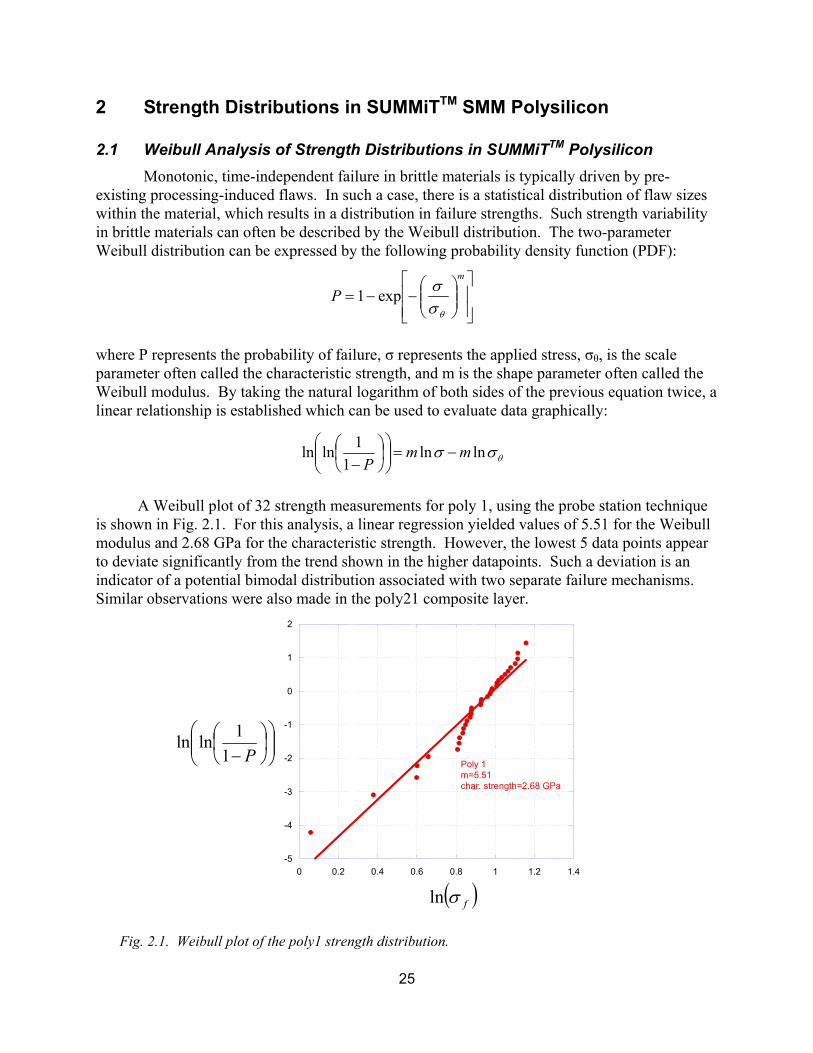
2 Strength Distributions in SUMMiTTM SMM Polysilicon 2.1 Weibull Analysis of Strength Distributions in SUMMiTTM Polysilicon
Monotonic, time-independent failure in brittle materials is typically driven by pre-existing processing-induced flaws. In such a case, there is a statistical distribution of flaw sizes within the material, which results in a distribution in failure strengths. Such strength variability in brittle materials can often be described by the Weibull distribution. The two-parameter Weibull distribution can be expressed by the following probability density function (PDF):
where P represents the probability of failure, σ represents the applied stress, σθ, is the scale parameter often called the characteristic strength, and m is the shape parameter often called the Weibull modulus. By taking the natural logarithm of both sides of the previous equation twice, a linear relationship is established which can be used to evaluate data graphically:
A Weibull plot of 32 strength measurements for poly 1, using the probe station technique
is shown in Fig. 2.1. For this analysis, a linear regression yielded values of 5.51 for the Weibull modulus and 2.68 GPa for the characteristic strength. However, the lowest 5 data points appear to deviate significantly from the trend shown in the higher datapoints. Such a deviation is an indicator of a potential bimodal distribution associated with two separate failure mechanisms. Similar observations were also made in the poly21 composite layer.
Fig. 2.1. Weibull plot of the poly1 strength distribution.
−−=
m
Pθσ
σexp1
θσσ lnln1
1lnln mmP
−=
−
− P11lnln
( )fσln
-5
-4
-3
-2
-1
0
1
2
0 0.2 0.4 0.6 0.8 1 1.2 1.4
Poly 1m=5.51char. strength=2.68 GPa
26
A bimodal strength distribution can be analyzed in separate parts using the maximum likelihood estimation method for Weibull parameters in a censored dataset, as described in ASTM C 1239 by solving the for the characteristic strength of the subset with r components:
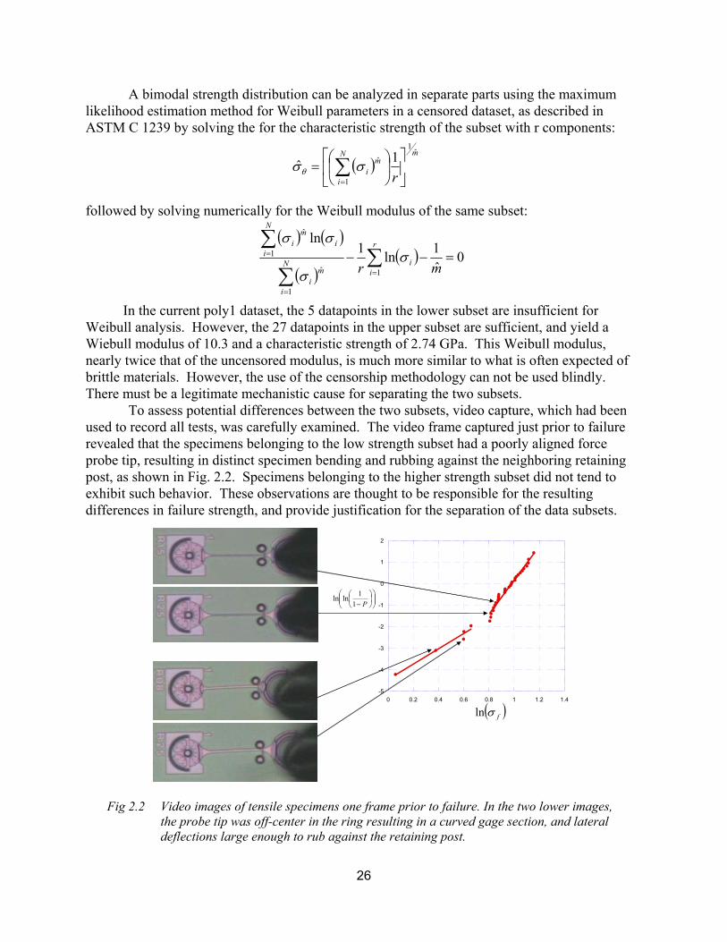
followed by solving numerically for the Weibull modulus of the same subset: In the current poly1 dataset, the 5 datapoints in the lower subset are insufficient for
Weibull analysis. However, the 27 datapoints in the upper subset are sufficient, and yield a Wiebull modulus of 10.3 and a characteristic strength of 2.74 GPa. This Weibull modulus, nearly twice that of the uncensored modulus, is much more similar to what is often expected of brittle materials. However, the use of the censorship methodology can not be used blindly. There must be a legitimate mechanistic cause for separating the two subsets.
To assess potential differences between the two subsets, video capture, which had been used to record all tests, was carefully examined. The video frame captured just prior to failure revealed that the specimens belonging to the low strength subset had a poorly aligned force probe tip, resulting in distinct specimen bending and rubbing against the neighboring retaining post, as shown in Fig. 2.2. Specimens belonging to the higher strength subset did not tend to exhibit such behavior. These observations are thought to be responsible for the resulting differences in failure strength, and provide justification for the separation of the data subsets.
Fig 2.2 Video images of tensile specimens one frame prior to failure. In the two lower images,
the probe tip was off-center in the ring resulting in a curved gage section, and lateral deflections large enough to rub against the retaining post.
( )mN
i
mi r
�1
1
� 1�
= ∑
=
σσθ
( ) ( )
( )( )∑
∑
∑=
=
= =−−r
iiN
i
mi
N
ii
mi
mr 1
1
�
1
�
0�1ln1
lnσ
σ
σσ
-5
-4
-3
-2
-1
0
1
2
0 0.2 0.4 0.6 0.8 1 1.2 1.4
− P11lnln
( )fσln
27
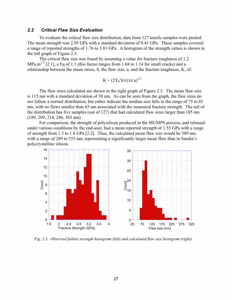
2.2 Critical Flaw Size Evaluation To evaluate the critical flaw size distribution, data from 127 tensile samples were pooled.
The mean strength was 2.95 GPa with a standard deviation of 0.41 GPa. These samples covered a range of reported strengths of 1.76 to 3.81 GPa. A histogram of the strength values is shown in the left graph of Figure 2.3.
The critical flaw size was found by assuming a value for fracture toughness of 1.2 MPa.m1/2 [2.1], a Fq of 1.1 (this factor ranges from 1.04 to 1.14 for small cracks) and a relationship between the mean stress, S, the flaw size, a, and the fracture toughness, K, of:
K = (2.Fθ
.S/π).(π.a)1/2 The flaw sizes calculated are shown in the right graph of Figure 2.3. The mean flaw size
is 115 nm with a standard deviation of 38 nm. As can be seen from the graph, the flaw sizes do not follow a normal distribution, but rather indicate the median size falls in the range of 75 to 85 nm, with no flaws smaller than 65 nm associated with the measured fracture strength. The tail of the distribution has five samples (out of 127) that had calculated flaw sizes larger than 185 nm (189, 209, 214, 246, 303 nm).
For comparison, the strength of polysilicon produced in the MUMPS process, and released under various conditions by the end-user, had a mean reported strength of 1.55 GPa with a range of strength from 1.3 to 1.8 GPa [2.2]. Thus, the calculated mean flaw size would be 389 nm, with a range of 289 to 553 nm, representing a significantly larger mean flaw than in Sandia�s polycrystalline silicon.
0
2
4
6
8
10
12
14
16
1.6 2 2.4 2.8 3.2 3.6 4
Cou
nt
Fracture Strength (GPa)
0
5
10
15
20
25
30
35
25 75 125 175 225 275 325
Cou
nt
Flaw size (nm)
Fig. 2.3. Observed failure strength histogram (left) and calculated flaw size histogram (right).
28
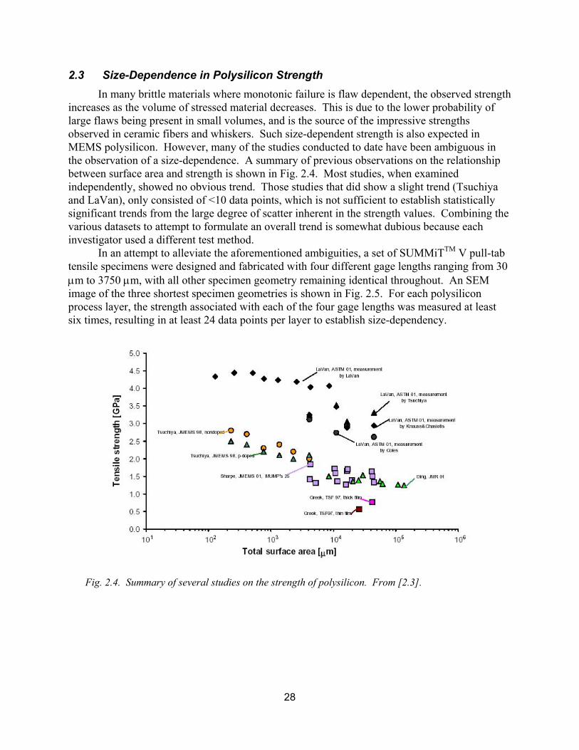
2.3 Size-Dependence in Polysilicon Strength In many brittle materials where monotonic failure is flaw dependent, the observed strength
increases as the volume of stressed material decreases. This is due to the lower probability of large flaws being present in small volumes, and is the source of the impressive strengths observed in ceramic fibers and whiskers. Such size-dependent strength is also expected in MEMS polysilicon. However, many of the studies conducted to date have been ambiguous in the observation of a size-dependence. A summary of previous observations on the relationship between surface area and strength is shown in Fig. 2.4. Most studies, when examined independently, showed no obvious trend. Those studies that did show a slight trend (Tsuchiya and LaVan), only consisted of <10 data points, which is not sufficient to establish statistically significant trends from the large degree of scatter inherent in the strength values. Combining the various datasets to attempt to formulate an overall trend is somewhat dubious because each investigator used a different test method.
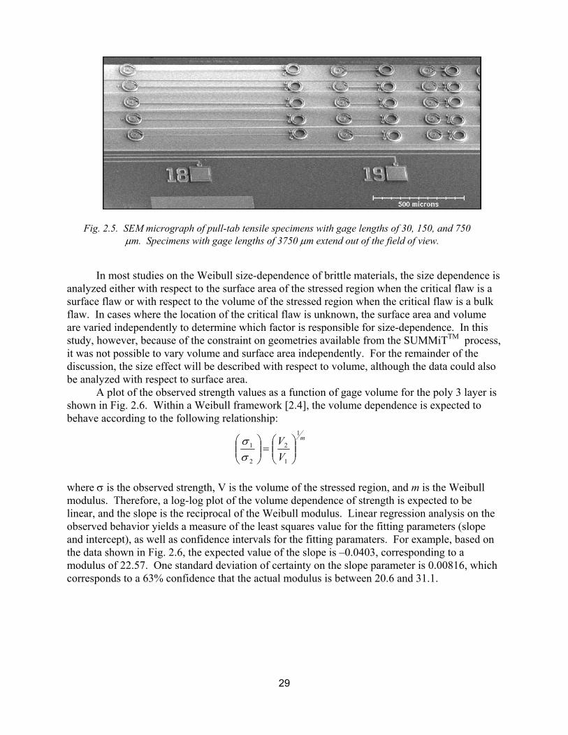
In an attempt to alleviate the aforementioned ambiguities, a set of SUMMiTTM V pull-tab tensile specimens were designed and fabricated with four different gage lengths ranging from 30 µm to 3750 µm, with all other specimen geometry remaining identical throughout. An SEM image of the three shortest specimen geometries is shown in Fig. 2.5. For each polysilicon process layer, the strength associated with each of the four gage lengths was measured at least six times, resulting in at least 24 data points per layer to establish size-dependency.
Fig. 2.4. Summary of several studies on the strength of polysilicon. From [2.3].
29
Fig. 2.5. SEM micrograph of pull-tab tensile specimens with gage lengths of 30, 150, and 750
µm. Specimens with gage lengths of 3750 µm extend out of the field of view.
In most studies on the Weibull size-dependence of brittle materials, the size dependence is analyzed either with respect to the surface area of the stressed region when the critical flaw is a surface flaw or with respect to the volume of the stressed region when the critical flaw is a bulk flaw. In cases where the location of the critical flaw is unknown, the surface area and volume are varied independently to determine which factor is responsible for size-dependence. In this study, however, because of the constraint on geometries available from the SUMMiTTM process, it was not possible to vary volume and surface area independently. For the remainder of the discussion, the size effect will be described with respect to volume, although the data could also be analyzed with respect to surface area.
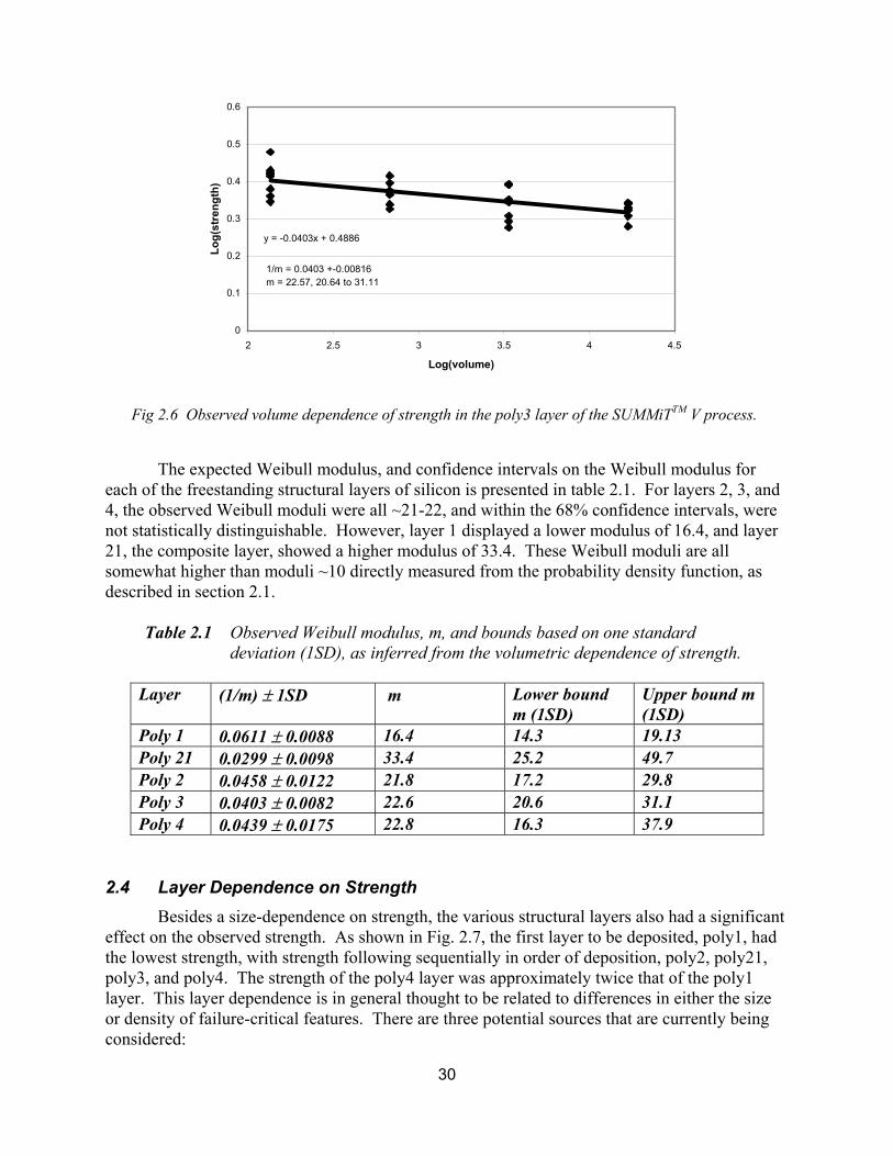
A plot of the observed strength values as a function of gage volume for the poly 3 layer is shown in Fig. 2.6. Within a Weibull framework [2.4], the volume dependence is expected to behave according to the following relationship:
where σ is the observed strength, V is the volume of the stressed region, and m is the Weibull modulus. Therefore, a log-log plot of the volume dependence of strength is expected to be linear, and the slope is the reciprocal of the Weibull modulus. Linear regression analysis on the observed behavior yields a measure of the least squares value for the fitting parameters (slope and intercept), as well as confidence intervals for the fitting paramaters. For example, based on the data shown in Fig. 2.6, the expected value of the slope is �0.0403, corresponding to a modulus of 22.57. One standard deviation of certainty on the slope parameter is 0.00816, which corresponds to a 63% confidence that the actual modulus is between 20.6 and 31.1.
m
VV
1
1
2
2
1
=
σσ
30
Fig 2.6 Observed volume dependence of strength in the poly3 layer of the SUMMiTTM V process.
The expected Weibull modulus, and confidence intervals on the Weibull modulus for each of the freestanding structural layers of silicon is presented in table 2.1. For layers 2, 3, and 4, the observed Weibull moduli were all ~21-22, and within the 68% confidence intervals, were not statistically distinguishable. However, layer 1 displayed a lower modulus of 16.4, and layer 21, the composite layer, showed a higher modulus of 33.4. These Weibull moduli are all somewhat higher than moduli ~10 directly measured from the probability density function, as described in section 2.1.
Table 2.1 Observed Weibull modulus, m, and bounds based on one standard
deviation (1SD), as inferred from the volumetric dependence of strength.
Layer (1/m) ± 1SD m Lower bound m (1SD)
Upper bound m (1SD)
Poly 1 0.0611 ± 0.0088 16.4 14.3 19.13 Poly 21 0.0299 ± 0.0098 33.4 25.2 49.7 Poly 2 0.0458 ± 0.0122 21.8 17.2 29.8 Poly 3 0.0403 ± 0.0082 22.6 20.6 31.1 Poly 4 0.0439 ± 0.0175 22.8 16.3 37.9
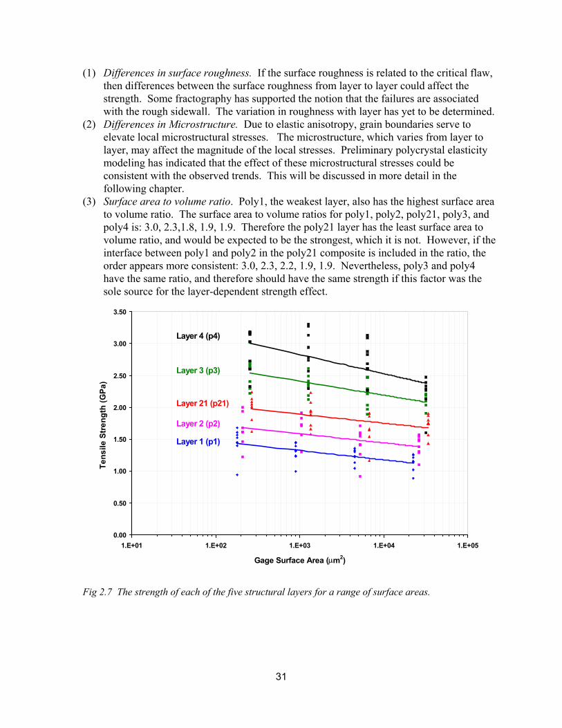
2.4 Layer Dependence on Strength Besides a size-dependence on strength, the various structural layers also had a significant
effect on the observed strength. As shown in Fig. 2.7, the first layer to be deposited, poly1, had the lowest strength, with strength following sequentially in order of deposition, poly2, poly21, poly3, and poly4. The strength of the poly4 layer was approximately twice that of the poly1 layer. This layer dependence is in general thought to be related to differences in either the size or density of failure-critical features. There are three potential sources that are currently being considered:
y = -0.0403x + 0.4886
0
0.1
0.2
0.3
0.4
0.5
0.6
2 2.5 3 3.5 4 4.5
Log(volume)
Log(
stre
ngth
)
1/m = 0.0403 +-0.00816m = 22.57, 20.64 to 31.11
31
(1) Differences in surface roughness. If the surface roughness is related to the critical flaw, then differences between the surface roughness from layer to layer could affect the strength. Some fractography has supported the notion that the failures are associated with the rough sidewall. The variation in roughness with layer has yet to be determined.
(2) Differences in Microstructure. Due to elastic anisotropy, grain boundaries serve to elevate local microstructural stresses. The microstructure, which varies from layer to layer, may affect the magnitude of the local stresses. Preliminary polycrystal elasticity modeling has indicated that the effect of these microstructural stresses could be consistent with the observed trends. This will be discussed in more detail in the following chapter.
(3) Surface area to volume ratio. Poly1, the weakest layer, also has the highest surface area to volume ratio. The surface area to volume ratios for poly1, poly2, poly21, poly3, and poly4 is: 3.0, 2.3,1.8, 1.9, 1.9. Therefore the poly21 layer has the least surface area to volume ratio, and would be expected to be the strongest, which it is not. However, if the interface between poly1 and poly2 in the poly21 composite is included in the ratio, the order appears more consistent: 3.0, 2.3, 2.2, 1.9, 1.9. Nevertheless, poly3 and poly4 have the same ratio, and therefore should have the same strength if this factor was the sole source for the layer-dependent strength effect.
Fig 2.7 The strength of each of the five structural layers for a range of surface areas.
0.00
0.50
1.00
1.50
2.00
2.50
3.00
3.50
1.E+01 1.E+02 1.E+03 1.E+04 1.E+05
Gage Surface Area (µm2)
Tens
ile S
tren
gth
(GPa
)
Layer 1 (p1)
Layer 2 (p2)
Layer 21 (p21)
Layer 3 (p3)
Layer 4 (p4)
32
2.5 References 2.1 Kahn, H., Tayebi, N., Ballarini, R., Mullen, R.L., and Heuer, A.H., �Fracture toughness of
polysilicon MEMS devices�, Sensors and Actuators, 82 (2000) 274-280. 2.2 Sharpe W.N., Jr., G. Coles, K. Jackson and R. Edwards, �Tensile Tests of Various Thin
Films,� in Mechanical Properties of Structural Films, ASTM STP 1413, C. Muhlstein and S. B. Brown, Eds., American Society for Testing and Materials, West Conshohocken, PA, 2001.
2.3 Bagdahn, J; Sharpe, WN; Jadaan, O, �Fracture strength of polysilicon at stress concentrations�, Journal of Microelectromechanical Systems, v.12, pp. 302-312, 2003.
2.4 W. Weibull, �A Statistical Distribution Function of Wide Applicability,� J. Appl. Mech. 18 (1951) p. 293.
33
3 The Role Of Microstructure In SUMMiTTM Polysilicon Failure
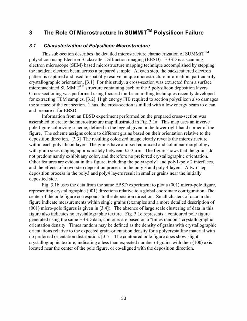
3.1 Characterization of Polysilicon Microstructure This sub-section describes the detailed microstructure characterization of SUMMiTTM
polysilicon using Electron Backscatter Diffraction imaging (EBSD). EBSD is a scanning electron microscope (SEM) based microstructure mapping technique accomplished by stepping the incident electron beam across a prepared sample. At each step, the backscattered electron pattern is captured and used to spatially resolve unique microstructure information, particularily crystallographic orientation. [3.1] For this study, a cross-section was extracted from a surface micromachined SUMMiTTM structure containing each of the 5 polysilicon deposition layers. Cross-sectioning was performed using focused ion-beam milling techniques recently developed for extracting TEM samples. [3.2] High energy FIB required to section polysilicon also damages the surface of the cut section. Thus, the cross-section is milled with a low energy beam to clean and prepare it for EBSD.
Information from an EBSD experiment performed on the prepared cross-section was assembled to create the microstructure map illustrated in Fig. 3.1a. This map uses an inverse pole figure colorizing scheme, defined in the legend given in the lower right-hand corner of the figure. The scheme assigns colors to different grains based on their orientation relative to the deposition direction. [3.3] The resulting colorized image clearly reveals the microstructure within each polysilicon layer. The grains have a mixed equi-axed and columnar morphology with grain sizes ranging approximately between 0.5-3 µm. The figure shows that the grains do not predominantly exhibit any color, and therefore no preferred crystallographic orientation. Other features are evident in this figure, including the poly0-poly1 and poly1-poly 2 interfaces, and the effects of a two-step deposition process in the poly 3 and poly 4 layers. A two-step deposition process in the poly3 and poly4 layers result in smaller grains near the initially deposited side.
Fig. 3.1b uses the data from the same EBSD experiment to plot a ⟨001⟩ micro-pole figure, representing crystallographic ⟨001⟩ directions relative to a global coordinate configuration. The center of the pole figure corresponds to the deposition direction. Small clusters of data in this figure indicate measurements within single grains (examples and a more detailed description of ⟨001⟩ micro-pole figures is given in [3.4]). The absence of large scale clustering of data in this figure also indicates no crystallographic texture. Fig. 3.1c represents a contoured pole figure generated using the same EBSD data, contours are based on a "times random" crystallographic orientation density. Times random may be defined as the density of grains with crystallographic orientations relative to the expected grain-orientation density for a polycrystalline material with no preferred orientation distribution. [3.5] The contoured pole figure does show slight crystallographic texture, indicating a less than expected number of grains with their ⟨100⟩ axis located near the center of the pole figure, or co-aligned with the deposition direction.
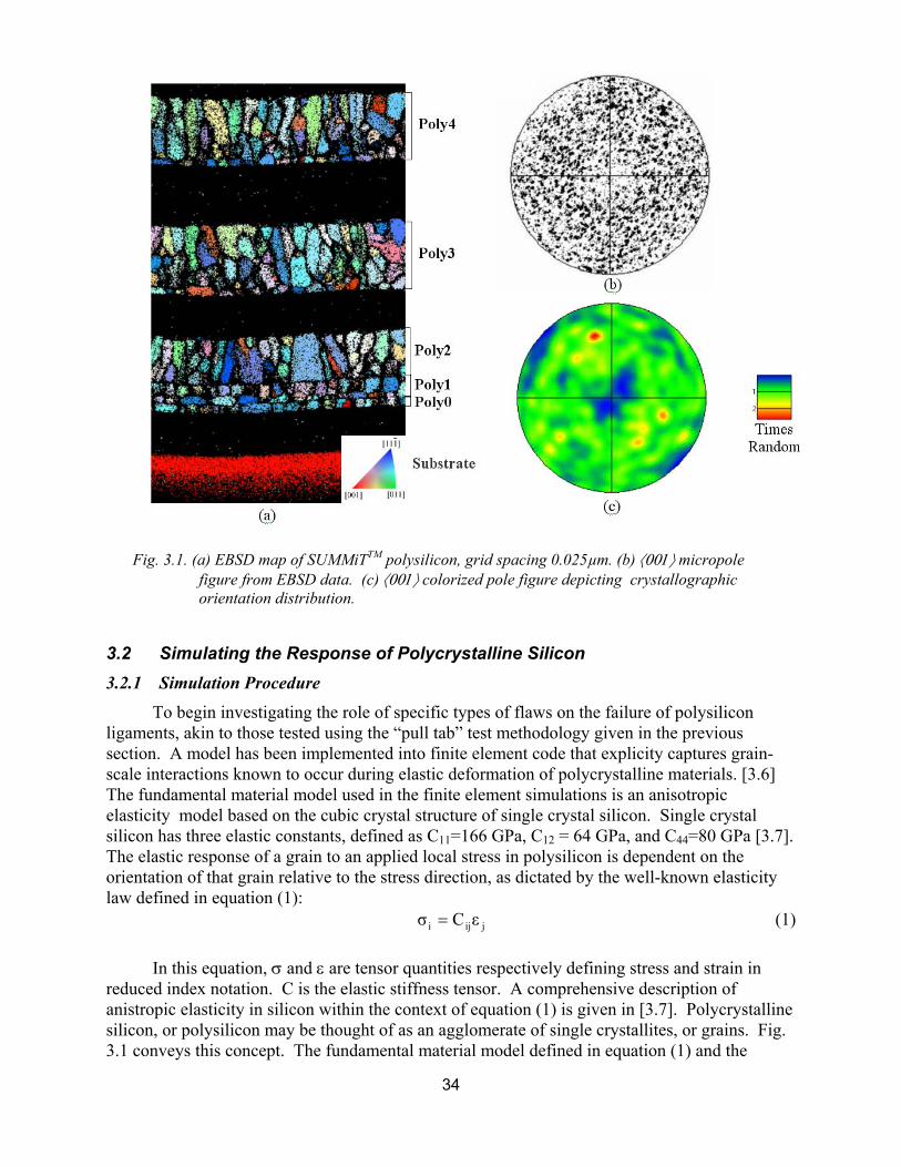
34
Fig. 3.1. (a) EBSD map of SUMMiTTM polysilicon, grid spacing 0.025µm. (b) ⟨001⟩ micropole
figure from EBSD data. (c) ⟨001⟩ colorized pole figure depicting crystallographic orientation distribution.
3.2 Simulating the Response of Polycrystalline Silicon 3.2.1 Simulation Procedure
To begin investigating the role of specific types of flaws on the failure of polysilicon ligaments, akin to those tested using the �pull tab� test methodology given in the previous section. A model has been implemented into finite element code that explicity captures grain-scale interactions known to occur during elastic deformation of polycrystalline materials. [3.6] The fundamental material model used in the finite element simulations is an anisotropic elasticity model based on the cubic crystal structure of single crystal silicon. Single crystal silicon has three elastic constants, defined as C11=166 GPa, C12 = 64 GPa, and C44=80 GPa [3.7]. The elastic response of a grain to an applied local stress in polysilicon is dependent on the orientation of that grain relative to the stress direction, as dictated by the well-known elasticity law defined in equation (1):
jiji εCσ = (1) In this equation, σ and ε are tensor quantities respectively defining stress and strain in
reduced index notation. C is the elastic stiffness tensor. A comprehensive description of anistropic elasticity in silicon within the context of equation (1) is given in [3.7]. Polycrystalline silicon, or polysilicon may be thought of as an agglomerate of single crystallites, or grains. Fig. 3.1 conveys this concept. The fundamental material model defined in equation (1) and the
35
crystallographic orientation of a grain, or finite element within a grain, determine its response to a local stress condition. Within a simulation, grain boundary intersections act as stress-concentrating flaws and, unless other geometric features are placed into the simulation, they dictate failure.
Fig. 3.2. Digitized microstructures mapped by EBSD for finite element analysis. (a) Section of a
joined poly1 and poly2 (poly12) layer and (b) section of a poly3 layer.
The EBSD map given in Fig. 3.1 was used as a template for generating finite element meshes to be used in the simulations. Sample microstructures representing the poly12 and poly3 layers were digitized using sections of the EBSD map as illustrated in Fig. 3.2. Finite element meshes were paved into these templates; thus, grain boundaries and free surfaces remained straight and sharp. Series of polycrystal elasticity simulations were performed using the meshed templates. The simulations were performed with periodic boundary conditions on the front and back faces; therefore, the simulations represent a microstructure infinite in extent. Top and bottom edges were treated as free surfaces, as they would be in real polysilicon ligaments. Displacement boundary conditions were placed on the left and right edges of the finite element meshes intended to replicate tension on a polysilicon ligament. These boundary conditions are illustrated in Fig. 3.3a. A randomly assigned crystallographic orientation was assigned to each grain within a polycrystal microstructure template prior to performing a simulation. The resultant crystallographic texture of the simulated polycystals was similar to the crystallographic texture of the SUMMiTTM polysilicon given by the EBSD experiment.
3.2.2 Results and Discussion
A simulated result, spatially resolved Von-Mises stress distribution in each polycrystal template after 1% tensile strain is given in Fig. 3.3. The stress-distribution varies widely across
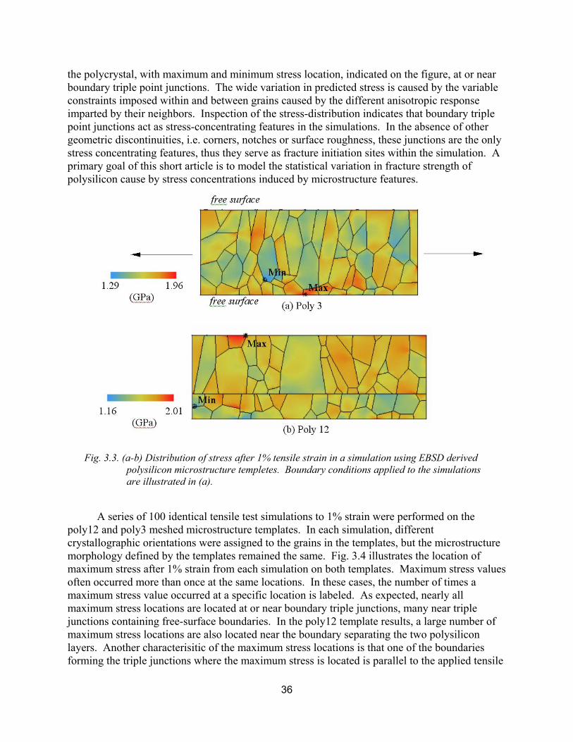
36
the polycrystal, with maximum and minimum stress location, indicated on the figure, at or near boundary triple point junctions. The wide variation in predicted stress is caused by the variable constraints imposed within and between grains caused by the different anisotropic response imparted by their neighbors. Inspection of the stress-distribution indicates that boundary triple point junctions act as stress-concentrating features in the simulations. In the absence of other geometric discontinuities, i.e. corners, notches or surface roughness, these junctions are the only stress concentrating features, thus they serve as fracture initiation sites within the simulation. A primary goal of this short article is to model the statistical variation in fracture strength of polysilicon cause by stress concentrations induced by microstructure features.
Fig. 3.3. (a-b) Distribution of stress after 1% tensile strain in a simulation using EBSD derived
polysilicon microstructure templetes. Boundary conditions applied to the simulations are illustrated in (a).
A series of 100 identical tensile test simulations to 1% strain were performed on the poly12 and poly3 meshed microstructure templates. In each simulation, different crystallographic orientations were assigned to the grains in the templates, but the microstructure morphology defined by the templates remained the same. Fig. 3.4 illustrates the location of maximum stress after 1% strain from each simulation on both templates. Maximum stress values often occurred more than once at the same locations. In these cases, the number of times a maximum stress value occurred at a specific location is labeled. As expected, nearly all maximum stress locations are located at or near boundary triple junctions, many near triple junctions containing free-surface boundaries. In the poly12 template results, a large number of maximum stress locations are also located near the boundary separating the two polysilicon layers. Another characterisitic of the maximum stress locations is that one of the boundaries forming the triple junctions where the maximum stress is located is parallel to the applied tensile
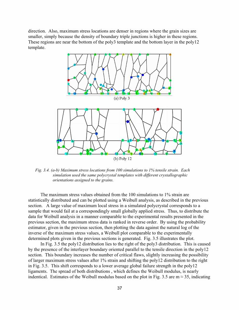
37
direction. Also, maximum stress locations are denser in regions where the grain sizes are smaller, simply because the density of boundary triple junctions is higher in these regions. These regions are near the bottom of the poly3 template and the bottom layer in the poly12 template.
Fig. 3.4. (a-b) Maximum stress locations from 100 simulations to 1% tensile strain. Each
simulation used the same polycrystal templates with different crystallographic orientations assigned to the grains.
The maximum stress values obtained from the 100 simulations to 1% strain are statistically distributed and can be plotted using a Weibull analysis, as described in the previous section. A large value of maximum local stress in a simulated polycrystal corresponds to a sample that would fail at a correspondingly small globally applied stress. Thus, to distribute the data for Weibull analysis in a manner comparable to the experimental results presented in the previous section, the maximum stress data is ranked in reverse order. By using the probability estimator, given in the previous section, then plotting the data against the natural log of the inverse of the maximum stress values, a Weibull plot comparable to the experimentally determined plots given in the previous sections is generated. Fig. 3.5 illustrates the plot.
In Fig. 3.5 the poly12 distribution lies to the right of the poly3 distribution. This is caused by the presence of the interlayer boundary oriented parallel to the tensile direction in the poly12 section. This boundary increases the number of critical flaws, slightly increasing the possibility of larger maximum stress values after 1% strain and shifting the poly12 distribution to the right in Fig. 3.5. This shift corresponds to a lower average global failure strength in the poly12 ligaments. The spread of both distributions , which defines the Weibull modulus, is nearly indentical. Estimates of the Weibull modulus based on the plot in Fig. 3.5 are m ≈ 35, indicating
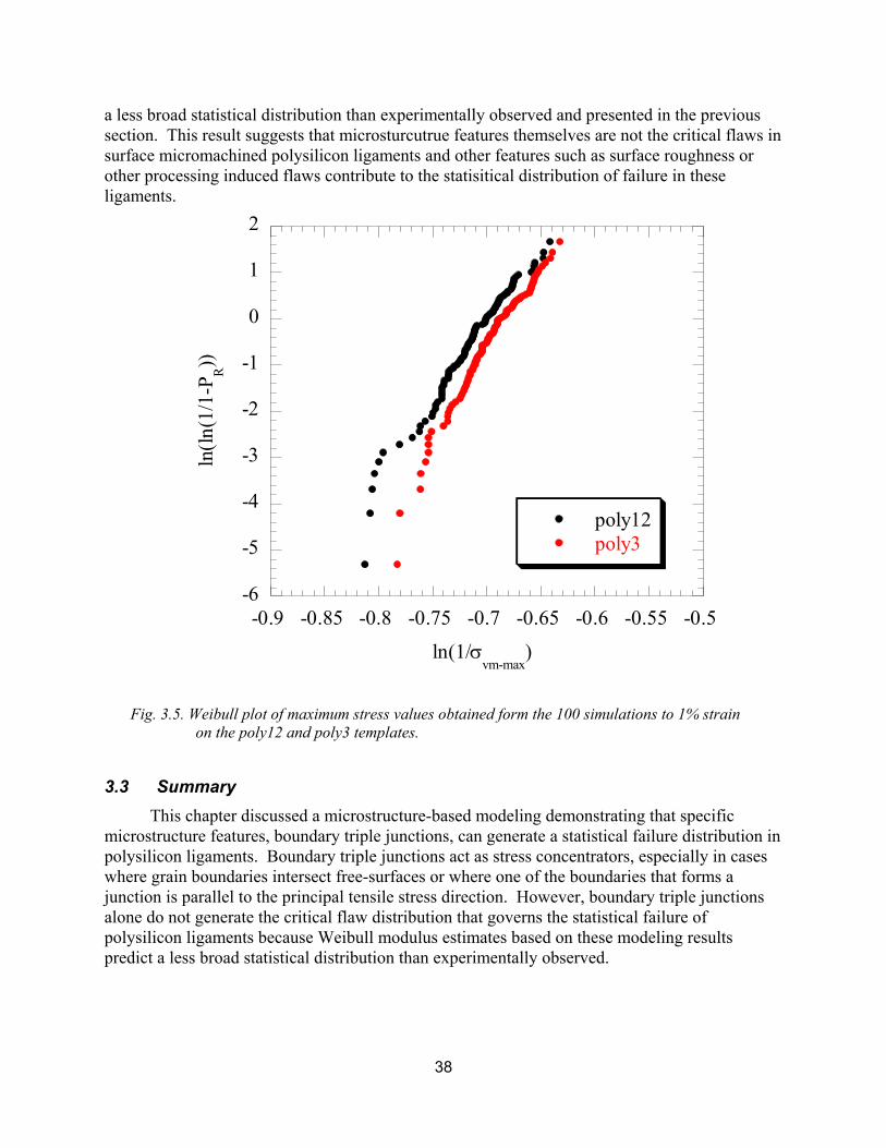
38
a less broad statistical distribution than experimentally observed and presented in the previous section. This result suggests that microsturcutrue features themselves are not the critical flaws in surface micromachined polysilicon ligaments and other features such as surface roughness or other processing induced flaws contribute to the statisitical distribution of failure in these ligaments.
Fig. 3.5. Weibull plot of maximum stress values obtained form the 100 simulations to 1% strain
on the poly12 and poly3 templates.
3.3 Summary This chapter discussed a microstructure-based modeling demonstrating that specific
microstructure features, boundary triple junctions, can generate a statistical failure distribution in polysilicon ligaments. Boundary triple junctions act as stress concentrators, especially in cases where grain boundaries intersect free-surfaces or where one of the boundaries that forms a junction is parallel to the principal tensile stress direction. However, boundary triple junctions alone do not generate the critical flaw distribution that governs the statistical failure of polysilicon ligaments because Weibull modulus estimates based on these modeling results predict a less broad statistical distribution than experimentally observed.
-0.9 -0.85 -0.8 -0.75 -0.7 -0.65 -0.6 -0.55 -0.5-6
-5
-4
-3
-2
-1
0
1
2
poly12poly3
ln(1/σvm-max
)
ln(ln
(1/1
-PR))
39
3.4 References 3.1 Randle, V., Microtexture Determination and its Applications, The Institute of Materials,
Portsmouth, London, 1992. 3.2 Phaneuf, M. W., (1999), Micron, 30, 221. 3.3 http://www.edax.com/technology/EBSD/OIM/index.html 3.4 Buchheit, T.E., LaVan, D.A., Michael, J.R., Christenson, T.R., and Leith S.D.,
"Microstructural and Mechanical Properties Investigation of Electrodeposited and Annealed LIGA Nickel Structures", Metallurgical and Materials Transactions A, Vol 33A, 2002, p. 539-553.
3.5 Hatherley, M. and Hutchinson, W.B., An Introduction to Textures in Metals, The Institution of Metallurgists, Monograph No. 5, Chameleon Press Ltd., London, 1979.
3.6 Espinosa, H.D. and Zavattieri, P.D., A Grain Level Model for the Study of Failure Initiation and Evolution in Polycrystalline Brittle Materials, Mechanics of Materials, v. 35, 2003, pp. 333-364.
3.7 Madou, M.J., Fundamentals of Microfabrication, Second Edition, CRC Press, London, 2002.
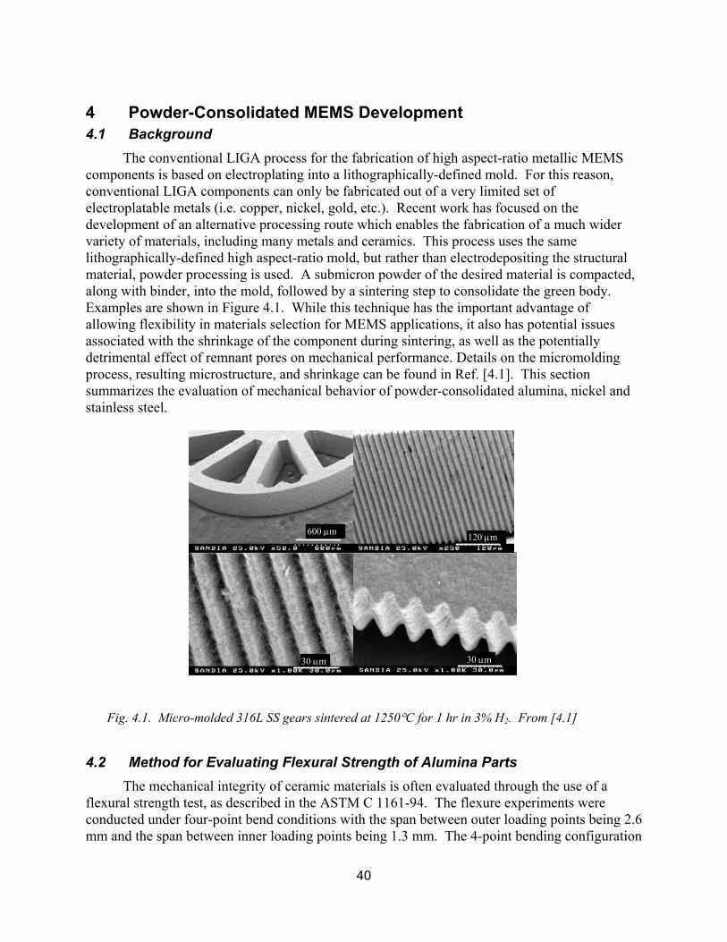
40
4 Powder-Consolidated MEMS Development 4.1 Background
The conventional LIGA process for the fabrication of high aspect-ratio metallic MEMS components is based on electroplating into a lithographically-defined mold. For this reason, conventional LIGA components can only be fabricated out of a very limited set of electroplatable metals (i.e. copper, nickel, gold, etc.). Recent work has focused on the development of an alternative processing route which enables the fabrication of a much wider variety of materials, including many metals and ceramics. This process uses the same lithographically-defined high aspect-ratio mold, but rather than electrodepositing the structural material, powder processing is used. A submicron powder of the desired material is compacted, along with binder, into the mold, followed by a sintering step to consolidate the green body. Examples are shown in Figure 4.1. While this technique has the important advantage of allowing flexibility in materials selection for MEMS applications, it also has potential issues associated with the shrinkage of the component during sintering, as well as the potentially detrimental effect of remnant pores on mechanical performance. Details on the micromolding process, resulting microstructure, and shrinkage can be found in Ref. [4.1]. This section summarizes the evaluation of mechanical behavior of powder-consolidated alumina, nickel and stainless steel.
Fig. 4.1. Micro-molded 316L SS gears sintered at 1250°C for 1 hr in 3% H2. From [4.1]
4.2 Method for Evaluating Flexural Strength of Alumina Parts The mechanical integrity of ceramic materials is often evaluated through the use of a
flexural strength test, as described in the ASTM C 1161-94. The flexure experiments were conducted under four-point bend conditions with the span between outer loading points being 2.6 mm and the span between inner loading points being 1.3 mm. The 4-point bending configuration
30 µm
120 µm
30 µm
600 µm
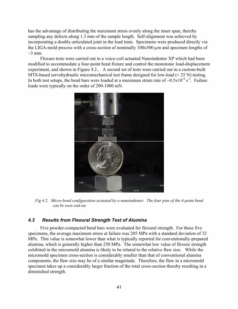
41
has the advantage of distributing the maximum stress evenly along the inner span, thereby sampling any defects along 1.3 mm of the sample length. Self-alignment was achieved by incorporating a doubly-articulated joint in the load train. Specimens were produced directly via the LIGA-mold process with a cross-section of nominally 100x500 µm and specimen lengths of ~3 mm.
Flexure tests were carried out in a voice-coil actuated Nanoindenter XP which had been modified to accommodate a four-point bend fixture and control the monotonic load-displacement experiment, and shown in Figure 4.2.. A second set of tests were carried out in a custom-built MTS-based servohydraulic micromechanical test frame designed for low-load (< 25 N) testing. In both test setups, the bend bars were loaded at a maximum strain rate of ~0.5x10⁻⁴ s-1. Failure loads were typically on the order of 200-1000 mN.
Fig 4.2. Micro-bend configuration actuated by a nanoindenter. The four pins of the 4-point bend
can be seen end-on.
4.3 Results from Flexural Strength Test of Alumina Five powder-compacted bend bars were evaluated for flexural strength. For these five
specimens, the average maximum stress at failure was 205 MPa with a standard deviation of 32 MPa. This value is somewhat lower than what is typically reported for conventionally-prepared alumina, which is generally higher than 250 MPa. The somewhat low value of flexure strength exhibited in the micromold alumina is likely to be related to the relative flaw size. While the micromold specimen cross-section is considerably smaller than that of conventional alumina components, the flaw size may be of a similar magnitude. Therefore, the flaw in a micromold specimen takes up a considerably larger fraction of the total cross-section thereby resulting in a diminished strength.
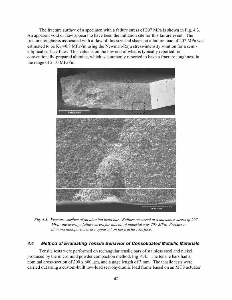
42
The fracture surface of a specimen with a failure stress of 207 MPa is shown in Fig. 4.3. An apparent void or flaw appears to have been the initiation site for this failure event. The fracture toughness associated with a flaw of this size and shape, at a failure load of 207 MPa was estimated to be KIC=0.8 MPa√m using the Newman-Raju stress-intensity solution for a semi-elliptical surface flaw. This value is on the low end of what is typically reported for conventionally-prepared alumina, which is commonly reported to have a fracture toughness in the range of 2-10 MPa√m.
Fig. 4.3. Fracture surface of an alumina bend bar. Failure occurred at a maximum stress of 207
MPa; the average failure stress for this lot of material was 205 MPa. Precursor alumina nanoparticles are apparent on the fracture surface.
4.4 Method of Evaluating Tensile Behavior of Consolidated Metallic Materials Tensile tests were performed on rectangular tensile bars of stainless steel and nickel
produced by the micromold powder compaction method, Fig 4.4.. The tensile bars had a nominal cross-section of 200 x 600 µm, and a gage length of 3 mm. The tensile tests were carried out using a custom-built low-load servohydraulic load frame based on an MTS actuator
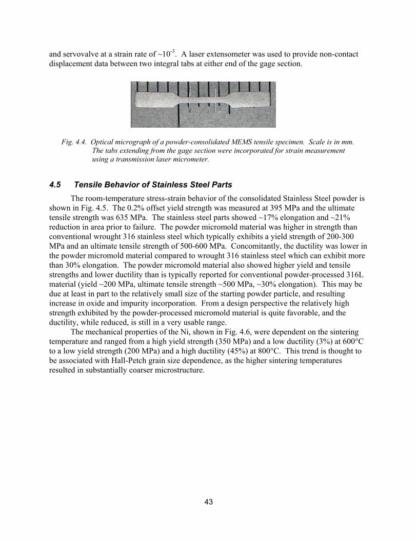
43
and servovalve at a strain rate of ~10-3. A laser extensometer was used to provide non-contact displacement data between two integral tabs at either end of the gage section.
Fig. 4.4. Optical micrograph of a powder-consolidated MEMS tensile specimen. Scale is in mm.
The tabs extending from the gage section were incorporated for strain measurement using a transmission laser micrometer.
4.5 Tensile Behavior of Stainless Steel Parts The room-temperature stress-strain behavior of the consolidated Stainless Steel powder is
shown in Fig. 4.5. The 0.2% offset yield strength was measured at 395 MPa and the ultimate tensile strength was 635 MPa. The stainless steel parts showed ~17% elongation and ~21% reduction in area prior to failure. The powder micromold material was higher in strength than conventional wrought 316 stainless steel which typically exhibits a yield strength of 200-300 MPa and an ultimate tensile strength of 500-600 MPa. Concomitantly, the ductility was lower in the powder micromold material compared to wrought 316 stainless steel which can exhibit more than 30% elongation. The powder micromold material also showed higher yield and tensile strengths and lower ductility than is typically reported for conventional powder-processed 316L material (yield ~200 MPa, ultimate tensile strength ~500 MPa, ~30% elongation). This may be due at least in part to the relatively small size of the starting powder particle, and resulting increase in oxide and impurity incorporation. From a design perspective the relatively high strength exhibited by the powder-processed micromold material is quite favorable, and the ductility, while reduced, is still in a very usable range.
The mechanical properties of the Ni, shown in Fig. 4.6, were dependent on the sintering temperature and ranged from a high yield strength (350 MPa) and a low ductility (3%) at 600°C to a low yield strength (200 MPa) and a high ductility (45%) at 800°C. This trend is thought to be associated with Hall-Petch grain size dependence, as the higher sintering temperatures resulted in substantially coarser microstructure.
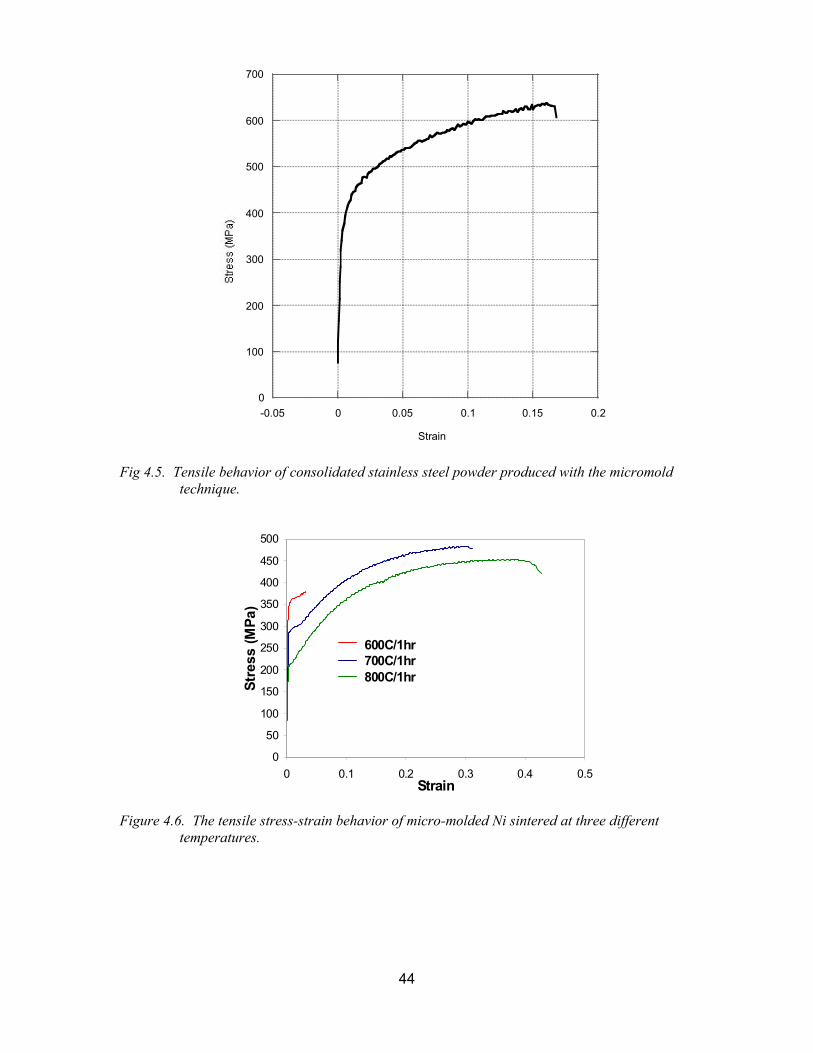
44
Fig 4.5. Tensile behavior of consolidated stainless steel powder produced with the micromold
technique.
Figure 4.6. The tensile stress-strain behavior of micro-molded Ni sintered at three different
temperatures.
0
100
200
300
400
500
600
700
-0.05 0 0.05 0.1 0.15 0.2 Strain
0
50
100
150
200
250
300
350
400
450
500
0 0.1 0.2 0.3 0.4 0.5Strain
Stre
ss (M
Pa)
600C/1hr700C/1hr800C/1hr

45
4.6 References 4.1. TJ Garino, AM Morales, and BL Boyce, �The Mechanical Properties, Dimensional
Tolerance and Microstructural Characterization of Micro-molded Ceramic and Metal Components�, submitted to Microsystems Technologies, June 2003.
46
5 EBSD Studies Of Wear-Induced Subsurfaces In Electroformed Nickel
5.1 Background
Many microelectromechanical systems (MEMS) fabricated by LIGA [German acronym for Lithography, Galvanoformung (electroforming) and Abformung (molding)] utilize electrodeposited metals such as nickel and Ni alloys. While Ni alloys may meet the structural requirements for MEMS, their tribological (friction and wear) behavior remains somewhat undefined. In a number of applications such as gear trains, comb drives and transmission linkages, tribological considerations, particularly sliding contacts amongst sidewalls, is of paramount importance. In ductile materials, sliding contact is often accompanied by large plastic strains resulting in subsurface layers whose microstructures could be dynamically altered during contact. The wear scars generated in load regimes relevant to LIGA MEMS applications are typically very small, and preparing cross sections of such small scars by conventional specimen preparation techniques for electron microscopy studies is practically impossible. In the current LDRD program, we have successfully applied focused ion beam (FIB) techniques to prepare wear scar cross sections at precise locations, and analyzed the subsurfaces by electron backscatter diffraction (EBSD). 5.2 Introduction
Plastic strains during sliding contact typically result in subsurface layers whose microstructures are different from those of the bulk [5.1-5.4]. Changes in the surface roughness, hardness, grain size and texture often occur during the initial run-in period, resulting in the evolution of a subsurface layer with characteristic features. Friction is, therefore, a time-dependent phenomenon until a steady state subsurface is evolved. Liu [5.5], Ringey and Hirth [5.1], and Khulman-Wilsdorf [5.6] have incorporated the effects of plastic deformation in the models on friction.
Microstructural evolution underneath wear surfaces has been the subject of numerous studies [5.1-5.11]. Heilmann, Clark and Rigney [5.8] studied the development of deformation substructure and orientation information (crystallographic texture) on worn copper samples by transmission electron microscopy (TEM). Similar studies were made by Rainforth and coworkers [5.9, 5.10] on a number of other single-phase metals (Fe, Al), alloys (Al-Si), metal-matrix composites and oxide ceramics. In all the above studies, large wear scars were generated under heavy loads (up to 200 N) using block-on-ring testers to facilitate cross sectional TEM specimen preparation by conventional methods. The specimen preparation techniques involved such aggressive steps as core drilling or dicing by a diamond saw, grinding, electropolishing and dimpling. Such specimen preparation techniques are not only cumbersome and extremely time consuming but also are inadequate in locating the substructures at a specific location on the wear surface. In a recent study, Farhat [5.11] evaluated the texture during wear using X-ray diffraction inverse pole figure techniques. Once again, the technique has the limitation when it comes to identifying the texture at a given location on the wear surface.
In recent years, focused ion beam (FIB) instrumentation has emerged as a novel tool for preparing samples for electron microscopy [5.12]. The objective of our current research was to explore the feasibility of FIB to make cross sections of wear surfaces suitable for electron
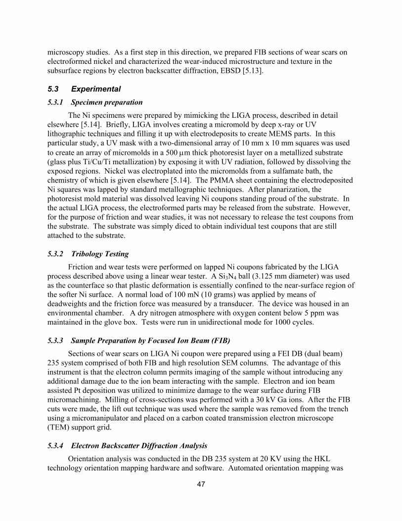
47
microscopy studies. As a first step in this direction, we prepared FIB sections of wear scars on electroformed nickel and characterized the wear-induced microstructure and texture in the subsurface regions by electron backscatter diffraction, EBSD [5.13].
5.3 Experimental 5.3.1 Specimen preparation
The Ni specimens were prepared by mimicking the LIGA process, described in detail elsewhere [5.14]. Briefly, LIGA involves creating a micromold by deep x-ray or UV lithographic techniques and filling it up with electrodeposits to create MEMS parts. In this particular study, a UV mask with a two-dimensional array of 10 mm x 10 mm squares was used to create an array of micromolds in a 500 µm thick photoresist layer on a metallized substrate (glass plus Ti/Cu/Ti metallization) by exposing it with UV radiation, followed by dissolving the exposed regions. Nickel was electroplated into the micromolds from a sulfamate bath, the chemistry of which is given elsewhere [5.14]. The PMMA sheet containing the electrodeposited Ni squares was lapped by standard metallographic techniques. After planarization, the photoresist mold material was dissolved leaving Ni coupons standing proud of the substrate. In the actual LIGA process, the electroformed parts may be released from the substrate. However, for the purpose of friction and wear studies, it was not necessary to release the test coupons from the substrate. The substrate was simply diced to obtain individual test coupons that are still attached to the substrate. 5.3.2 Tribology Testing
Friction and wear tests were performed on lapped Ni coupons fabricated by the LIGA process described above using a linear wear tester. A Si3N4 ball (3.125 mm diameter) was used as the counterface so that plastic deformation is essentially confined to the near-surface region of the softer Ni surface. A normal load of 100 mN (10 grams) was applied by means of deadweights and the friction force was measured by a transducer. The device was housed in an environmental chamber. A dry nitrogen atmosphere with oxygen content below 5 ppm was maintained in the glove box. Tests were run in unidirectional mode for 1000 cycles.
5.3.3 Sample Preparation by Focused Ion Beam (FIB)
Sections of wear scars on LIGA Ni coupon were prepared using a FEI DB (dual beam) 235 system comprised of both FIB and high resolution SEM columns. The advantage of this instrument is that the electron column permits imaging of the sample without introducing any additional damage due to the ion beam interacting with the sample. Electron and ion beam assisted Pt deposition was utilized to minimize damage to the wear surface during FIB micromachining. Milling of cross-sections was performed with a 30 kV Ga ions. After the FIB cuts were made, the lift out technique was used where the sample was removed from the trench using a micromanipulator and placed on a carbon coated transmission electron microscope (TEM) support grid.
5.3.4 Electron Backscatter Diffraction Analysis
Orientation analysis was conducted in the DB 235 system at 20 KV using the HKL technology orientation mapping hardware and software. Automated orientation mapping was
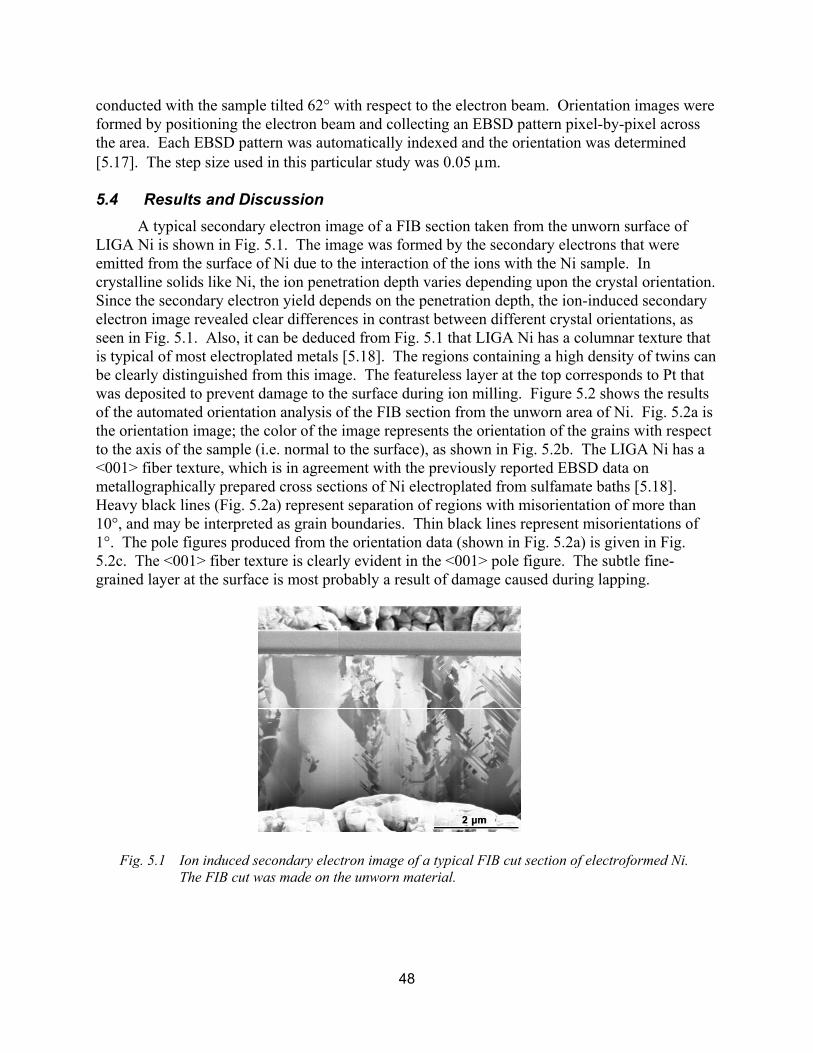
48
conducted with the sample tilted 62° with respect to the electron beam. Orientation images were formed by positioning the electron beam and collecting an EBSD pattern pixel-by-pixel across the area. Each EBSD pattern was automatically indexed and the orientation was determined [5.17]. The step size used in this particular study was 0.05 µm.
5.4 Results and Discussion
A typical secondary electron image of a FIB section taken from the unworn surface of LIGA Ni is shown in Fig. 5.1. The image was formed by the secondary electrons that were emitted from the surface of Ni due to the interaction of the ions with the Ni sample. In crystalline solids like Ni, the ion penetration depth varies depending upon the crystal orientation. Since the secondary electron yield depends on the penetration depth, the ion-induced secondary electron image revealed clear differences in contrast between different crystal orientations, as seen in Fig. 5.1. Also, it can be deduced from Fig. 5.1 that LIGA Ni has a columnar texture that is typical of most electroplated metals [5.18]. The regions containing a high density of twins can be clearly distinguished from this image. The featureless layer at the top corresponds to Pt that was deposited to prevent damage to the surface during ion milling. Figure 5.2 shows the results of the automated orientation analysis of the FIB section from the unworn area of Ni. Fig. 5.2a is the orientation image; the color of the image represents the orientation of the grains with respect to the axis of the sample (i.e. normal to the surface), as shown in Fig. 5.2b. The LIGA Ni has a <001> fiber texture, which is in agreement with the previously reported EBSD data on metallographically prepared cross sections of Ni electroplated from sulfamate baths [5.18]. Heavy black lines (Fig. 5.2a) represent separation of regions with misorientation of more than 10°, and may be interpreted as grain boundaries. Thin black lines represent misorientations of 1°. The pole figures produced from the orientation data (shown in Fig. 5.2a) is given in Fig. 5.2c. The <001> fiber texture is clearly evident in the <001> pole figure. The subtle fine-grained layer at the surface is most probably a result of damage caused during lapping.
Fig. 5.1 Ion induced secondary electron image of a typical FIB cut section of electroformed Ni.
The FIB cut was made on the unworn material.
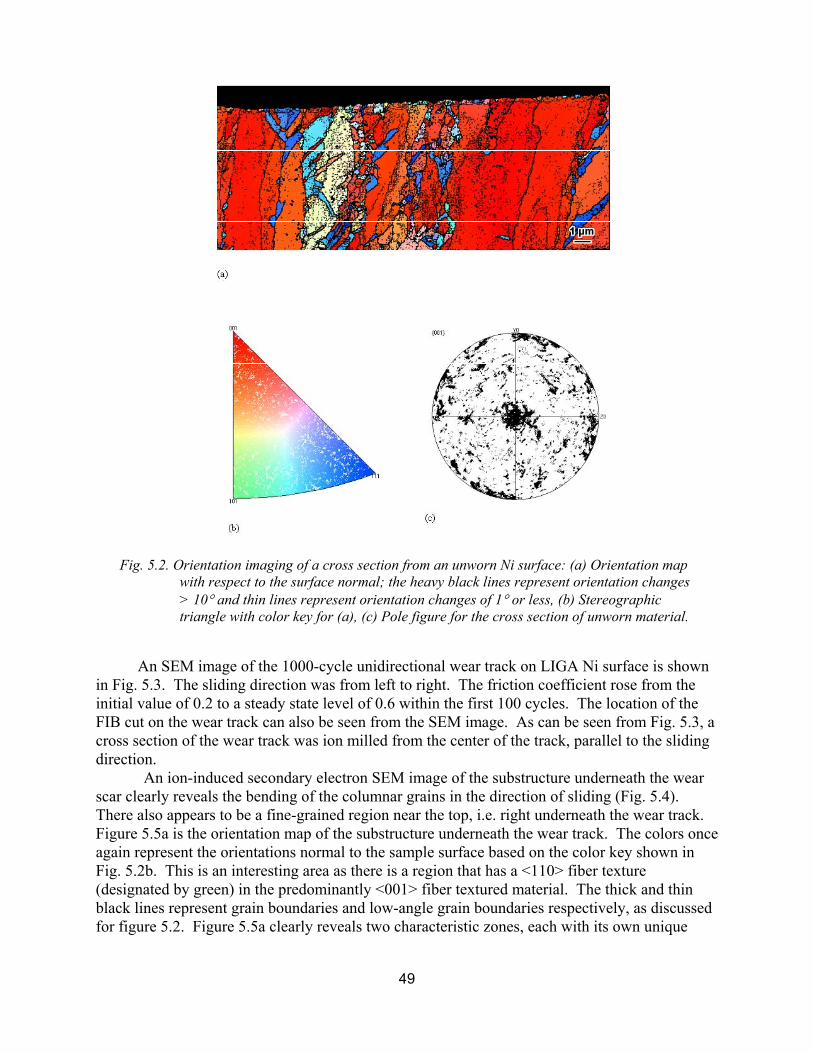
49
Fig. 5.2. Orientation imaging of a cross section from an unworn Ni surface: (a) Orientation map
with respect to the surface normal; the heavy black lines represent orientation changes > 10° and thin lines represent orientation changes of 1° or less, (b) Stereographic triangle with color key for (a), (c) Pole figure for the cross section of unworn material.
An SEM image of the 1000-cycle unidirectional wear track on LIGA Ni surface is shown in Fig. 5.3. The sliding direction was from left to right. The friction coefficient rose from the initial value of 0.2 to a steady state level of 0.6 within the first 100 cycles. The location of the FIB cut on the wear track can also be seen from the SEM image. As can be seen from Fig. 5.3, a cross section of the wear track was ion milled from the center of the track, parallel to the sliding direction.
An ion-induced secondary electron SEM image of the substructure underneath the wear scar clearly reveals the bending of the columnar grains in the direction of sliding (Fig. 5.4). There also appears to be a fine-grained region near the top, i.e. right underneath the wear track. Figure 5.5a is the orientation map of the substructure underneath the wear track. The colors once again represent the orientations normal to the sample surface based on the color key shown in Fig. 5.2b. This is an interesting area as there is a region that has a <110> fiber texture (designated by green) in the predominantly <001> fiber textured material. The thick and thin black lines represent grain boundaries and low-angle grain boundaries respectively, as discussed for figure 5.2. Figure 5.5a clearly reveals two characteristic zones, each with its own unique
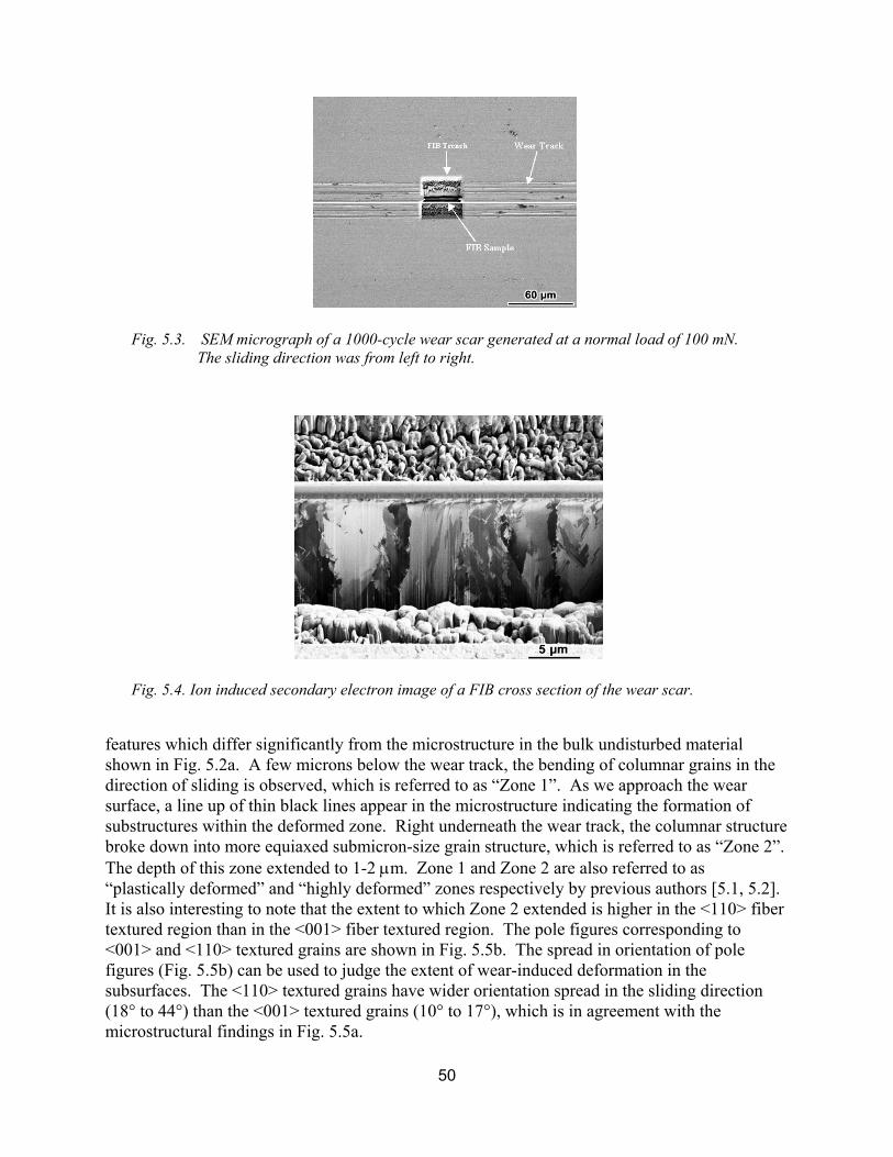
50
Fig. 5.3. SEM micrograph of a 1000-cycle wear scar generated at a normal load of 100 mN.
The sliding direction was from left to right.
Fig. 5.4. Ion induced secondary electron image of a FIB cross section of the wear scar.
features which differ significantly from the microstructure in the bulk undisturbed material shown in Fig. 5.2a. A few microns below the wear track, the bending of columnar grains in the direction of sliding is observed, which is referred to as �Zone 1�. As we approach the wear surface, a line up of thin black lines appear in the microstructure indicating the formation of substructures within the deformed zone. Right underneath the wear track, the columnar structure broke down into more equiaxed submicron-size grain structure, which is referred to as �Zone 2�. The depth of this zone extended to 1-2 µm. Zone 1 and Zone 2 are also referred to as �plastically deformed� and �highly deformed� zones respectively by previous authors [5.1, 5.2]. It is also interesting to note that the extent to which Zone 2 extended is higher in the <110> fiber textured region than in the <001> fiber textured region. The pole figures corresponding to <001> and <110> textured grains are shown in Fig. 5.5b. The spread in orientation of pole figures (Fig. 5.5b) can be used to judge the extent of wear-induced deformation in the subsurfaces. The <110> textured grains have wider orientation spread in the sliding direction (18° to 44°) than the <001> textured grains (10° to 17°), which is in agreement with the microstructural findings in Fig. 5.5a.
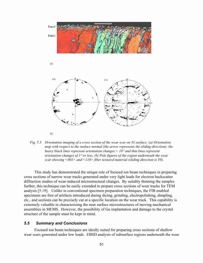
51
Fig. 5.5. Orientation imaging of a cross section of the wear scar on Ni surface: (a) Orientation
map with respect to the surface normal (the arrow represents the sliding direction); the heavy black lines represent orientation changes > 10° and thin lines represent orientation changes of 1° or less, (b) Pole figures of the region underneath the wear scar showing <001> and <110> fiber textured material (sliding direction is Y0).
This study has demonstrated the unique role of focused ion beam techniques in preparing cross sections of narrow wear tracks generated under very light loads for electron backscatter diffraction studies of wear-induced microstructural changes. By suitably thinning the samples further, this technique can be easily extended to prepare cross sections of wear tracks for TEM analysis [5.19]. Unlike in conventional specimen preparation techniques, the FIB enabled specimens are free of artifacts introduced during dicing, grinding, electropolishing, dimpling, etc., and sections can be precisely cut at a specific location on the wear track. This capability is extremely valuable in characterizing the near surface microstructures of moving mechanical assemblies in MEMS. However, the possibility of Ga implantation and damage to the crystal structure of the sample must be kept in mind.
5.5 Summary and Conclusions
Focused ion beam techniques are ideally suited for preparing cross sections of shallow wear scars generated under low loads. EBSD analysis of subsurface regions underneath the wear
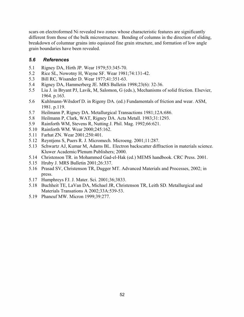
52
scars on electroformed Ni revealed two zones whose characteristic features are significantly different from those of the bulk microstructure. Bending of columns in the direction of sliding, breakdown of columnar grains into equiaxed fine grain structure, and formation of low angle grain boundaries have been revealed.
5.6 References 5.1 Rigney DA, Hirth JP. Wear 1979;53:345-70. 5.2 Rice SL, Nowotny H, Wayne SF. Wear 1981;74:131-42. 5.3 Bill RC, Wisander D. Wear 1977;41:351-63. 5.4 Rigney DA, Hammerberg JE. MRS Bulletin 1998;23(6): 32-36. 5.5 Liu J. in Bryant PJ, Lavik, M, Salomon, G (eds.), Mechanisms of solid friction. Elsevier,
1964. p.163. 5.6 Kuhlmann-Wilsdorf D. in Rigeny DA. (ed.) Fundamentals of friction and wear. ASM,
1981. p.119. 5.7 Heilmann P, Rigney DA. Metallurgical Transactions 1981;12A:686. 5.8 Heilmann P, Clark, WAT, Rigney DA. Acta Metall. 1983;31:1293. 5.9 Rainforth WM, Stevens R, Nutting J. Phil. Mag. 1992;66:621. 5.10 Rainforth WM. Wear 2000;245:162. 5.11 Farhat ZN. Wear 2001;250:401. 5.12 Reyntjens S, Puers R. J. Micromech. Microeng. 2001;11:287. 5.13 Schwartz AJ, Kumar M, Adams BL. Electron backscatter diffraction in materials science.
Kluwer Academic/Plenum Publishers; 2000. 5.14 Christenson TR. in Mohammed Gad-el-Hak (ed.) MEMS handbook. CRC Press. 2001. 5.15 Hruby J. MRS Bulletin 2001;26:337. 5.16 Prasad SV, Christenson TR, Dugger MT. Advanced Materials and Processes, 2002; in
press. 5.17 Humphreys FJ. J. Mater. Sci. 2001;36;3833. 5.18 Buchheit TE, LaVan DA, Michael JR, Christenson TR, Leith SD. Metallurgical and
Materials Transations A 2002;33A:539-53. 5.19 Phaneuf MW. Micron 1999;39:277.
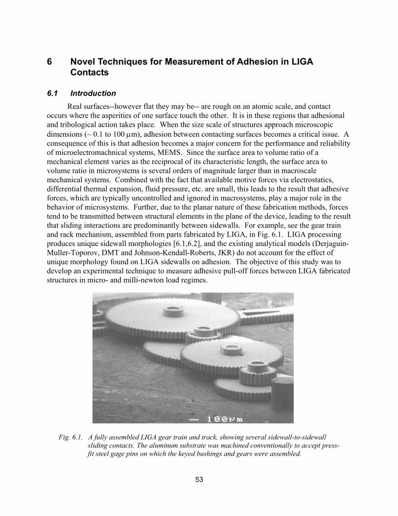
53
6 Novel Techniques for Measurement of Adhesion in LIGA
Contacts 6.1 Introduction
Real surfaces--however flat they may be-- are rough on an atomic scale, and contact occurs where the asperities of one surface touch the other. It is in these regions that adhesional and tribological action takes place. When the size scale of structures approach microscopic dimensions (~ 0.1 to 100 µm), adhesion between contacting surfaces becomes a critical issue. A consequence of this is that adhesion becomes a major concern for the performance and reliability of microelectromachnical systems, MEMS. Since the surface area to volume ratio of a mechanical element varies as the reciprocal of its characteristic length, the surface area to volume ratio in microsystems is several orders of magnitude larger than in macroscale mechanical systems. Combined with the fact that available motive forces via electrostatics, differential thermal expansion, fluid pressure, etc. are small, this leads to the result that adhesive forces, which are typically uncontrolled and ignored in macrosystems, play a major role in the behavior of microsystems. Further, due to the planar nature of these fabrication methods, forces tend to be transmitted between structural elements in the plane of the device, leading to the result that sliding interactions are predominantly between sidewalls. For example, see the gear train and rack mechanism, assembled from parts fabricated by LIGA, in Fig. 6.1. LIGA processing produces unique sidewall morphologies [6.1,6.2], and the existing analytical models (Derjaguin-Muller-Toporov, DMT and Johnson-Kendall-Roberts, JKR) do not account for the effect of unique morphology found on LIGA sidewalls on adhesion. The objective of this study was to develop an experimental technique to measure adhesive pull-off forces between LIGA fabricated structures in micro- and milli-newton load regimes.
Fig. 6.1. A fully assembled LIGA gear train and track, showing several sidewall-to-sidewall
sliding contacts. The aluminum substrate was machined conventionally to accept press-fit steel gage pins on which the keyed bushings and gears were assembled.
54
6.2 A Review of Analytical Models It is widely recognized that under the action of surface forces the surfaces are drawn
together and a finite area of contact is established for zero applied load. In JKR model [6.3], the shape of the contact is quite different from that associated with Hertzian deformation and shows a small neck around the contact zone (Fig. 6.2b). If an external load is applied, the contact area is increased but on reducing the load it decreases reversibly. If the external load is made negative, the area of contact diminishes until an instability occurs at a finite size of the contact circle and the surfaces pull apart. The major difference between this (JKR model) and the DMT model is that the later assumes Hertzian deformation is not modified by the surface forces (Fig. 6.2a). The pull-off force from JKR model is comparable with, but smaller than, that given by the DMT model, Fig. 6.2c, [6.4, 6.5]. Neither of the two models predicts the role surface morphology on adhesion.
Fig. 6.2. Contact between an elastic sphere and a rigid flat in the presence of surface forces: (a)
the DMT model; (b) the JKR model; (c) the change in radius of contact as a function of applied load.
The classical work in the field of adhesion of rough surfaces is that of Fuller and Tabor [6.6], who showed experimentally that higher surface roughness could actually give rise to lower adhesion force. Using the theoretical approach of Greenwood and Williamson [6.7] for asperity related issues, and the JKR formulas of adhesive contact of two spheres [6.3], Fuller and Tabor [6.6] arrived at a non-dimensional adhesion parameter, θ, defined as:
WE
ββσθ
21
23
=
where E is the effective elastic modulus, σ is the standard deviation of asperity heights from an average datum plane, β is the radius of curvature of individual asperity, and W is the work of adhesion ( W = γ1 + γ2 � γ12, where γ1 and γ2 are the surface energies of the individual surfaces of the contacting materials, and γ12 is the surface energy of the interface). Low adhesion occurs for a high value of adhesion parameter, θ, and equation (1) shows that this can be accomplished with: (i) high elastic modulus of the materials (or possibly a high modulus coating on a lower modulus substrate), (ii) a high value of σ, i.e., high surface roughness, (iii) a low value of work
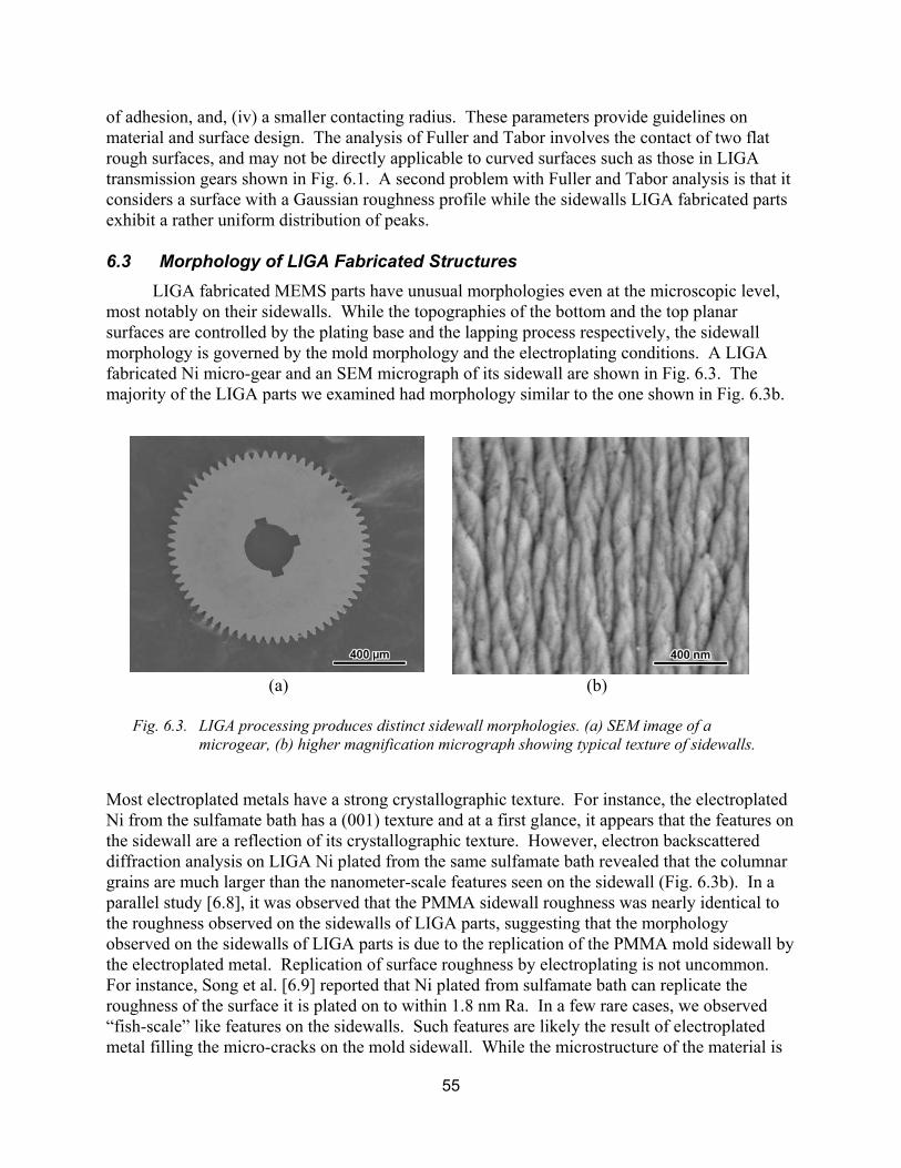
55
of adhesion, and, (iv) a smaller contacting radius. These parameters provide guidelines on material and surface design. The analysis of Fuller and Tabor involves the contact of two flat rough surfaces, and may not be directly applicable to curved surfaces such as those in LIGA transmission gears shown in Fig. 6.1. A second problem with Fuller and Tabor analysis is that it considers a surface with a Gaussian roughness profile while the sidewalls LIGA fabricated parts exhibit a rather uniform distribution of peaks. 6.3 Morphology of LIGA Fabricated Structures
LIGA fabricated MEMS parts have unusual morphologies even at the microscopic level, most notably on their sidewalls. While the topographies of the bottom and the top planar surfaces are controlled by the plating base and the lapping process respectively, the sidewall morphology is governed by the mold morphology and the electroplating conditions. A LIGA fabricated Ni micro-gear and an SEM micrograph of its sidewall are shown in Fig. 6.3. The majority of the LIGA parts we examined had morphology similar to the one shown in Fig. 6.3b.
(a) (b)
Fig. 6.3. LIGA processing produces distinct sidewall morphologies. (a) SEM image of a microgear, (b) higher magnification micrograph showing typical texture of sidewalls.
Most electroplated metals have a strong crystallographic texture. For instance, the electroplated Ni from the sulfamate bath has a (001) texture and at a first glance, it appears that the features on the sidewall are a reflection of its crystallographic texture. However, electron backscattered diffraction analysis on LIGA Ni plated from the same sulfamate bath revealed that the columnar grains are much larger than the nanometer-scale features seen on the sidewall (Fig. 6.3b). In a parallel study [6.8], it was observed that the PMMA sidewall roughness was nearly identical to the roughness observed on the sidewalls of LIGA parts, suggesting that the morphology observed on the sidewalls of LIGA parts is due to the replication of the PMMA mold sidewall by the electroplated metal. Replication of surface roughness by electroplating is not uncommon. For instance, Song et al. [6.9] reported that Ni plated from sulfamate bath can replicate the roughness of the surface it is plated on to within 1.8 nm Ra. In a few rare cases, we observed �fish-scale� like features on the sidewalls. Such features are likely the result of electroplated metal filling the micro-cracks on the mold sidewall. While the microstructure of the material is
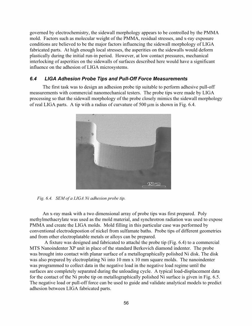
56
governed by electrochemistry, the sidewall morphology appears to be controlled by the PMMA mold. Factors such as molecular weight of the PMMA, residual stresses, and x-ray exposure conditions are believed to be the major factors influencing the sidewall morphology of LIGA fabricated parts. At high enough local stresses, the asperities on the sidewalls would deform plastically during the initial run-in period. However, at low contact pressures, mechanical interlocking of asperities on the sidewalls of surfaces described here would have a significant influence on the adhesion of LIGA microsystems. 6.4 LIGA Adhesion Probe Tips and Pull-Off Force Measurements
The first task was to design an adhesion probe tip suitable to perform adhesive pull-off measurements with commercial nanomechanical testers. The probe tips were made by LIGA processing so that the sidewall morphology of the probe closely mimics the sidewall morphology of real LIGA parts. A tip with a radius of curvature of 500 µm is shown in Fig. 6.4.
Fig. 6.4. SEM of a LIGA Ni adhesion probe tip.
An x-ray mask with a two dimensional array of probe tips was first prepared. Poly methylmethacrylate was used as the mold material, and synchrotron radiation was used to expose PMMA and create the LIGA molds. Mold filling in this particular case was performed by conventional electrodepostion of nickel from sulfamate baths. Probe tips of different geometries and from other electroplatable metals or alloys can be prepared.
A fixture was designed and fabricated to attaché the probe tip (Fig. 6.4) to a commercial MTS Nanoindenter XP unit in place of the standard Berkovich diamond indenter. The probe was brought into contact with planar surface of a metallographically polished Ni disk. The disk was also prepared by electroplating Ni into 10 mm x 10 mm square molds. The nanoindenter was programmed to collect data in the negative load in the negative load regime until the surfaces are completely separated during the unloading cycle. A typical load-displacement data for the contact of the Ni probe tip on metallographically polished Ni surface is given in Fig. 6.5. The negative load or pull-off force can be used to guide and validate analytical models to predict adhesion between LIGA fabricated parts.
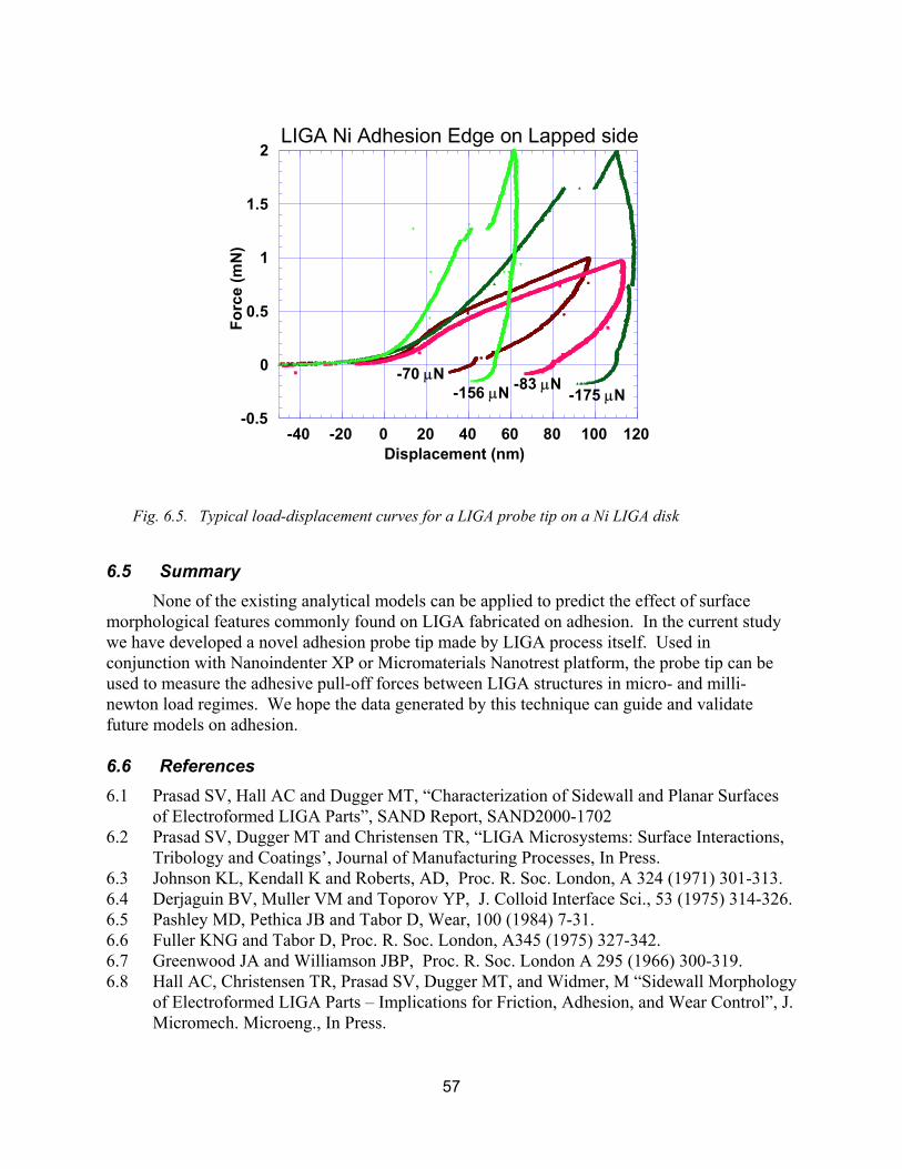
57
Fig. 6.5. Typical load-displacement curves for a LIGA probe tip on a Ni LIGA disk
6.5 Summary None of the existing analytical models can be applied to predict the effect of surface
morphological features commonly found on LIGA fabricated on adhesion. In the current study we have developed a novel adhesion probe tip made by LIGA process itself. Used in conjunction with Nanoindenter XP or Micromaterials Nanotrest platform, the probe tip can be used to measure the adhesive pull-off forces between LIGA structures in micro- and milli-newton load regimes. We hope the data generated by this technique can guide and validate future models on adhesion.
6.6 References 6.1 Prasad SV, Hall AC and Dugger MT, �Characterization of Sidewall and Planar Surfaces
of Electroformed LIGA Parts�, SAND Report, SAND2000-1702 6.2 Prasad SV, Dugger MT and Christensen TR, �LIGA Microsystems: Surface Interactions,
Tribology and Coatings�, Journal of Manufacturing Processes, In Press. 6.3 Johnson KL, Kendall K and Roberts, AD, Proc. R. Soc. London, A 324 (1971) 301-313. 6.4 Derjaguin BV, Muller VM and Toporov YP, J. Colloid Interface Sci., 53 (1975) 314-326. 6.5 Pashley MD, Pethica JB and Tabor D, Wear, 100 (1984) 7-31. 6.6 Fuller KNG and Tabor D, Proc. R. Soc. London, A345 (1975) 327-342. 6.7 Greenwood JA and Williamson JBP, Proc. R. Soc. London A 295 (1966) 300-319. 6.8 Hall AC, Christensen TR, Prasad SV, Dugger MT, and Widmer, M �Sidewall Morphology
of Electroformed LIGA Parts � Implications for Friction, Adhesion, and Wear Control�, J. Micromech. Microeng., In Press.
-0.5
0
0.5
1
1.5
2
-40 -20 0 20 40 60 80 100 120
LIGA Ni Adhesion Edge on Lapped side
Forc
e (m
N)
Displacement (nm)
-70 µN-175 µN-156 µN -83 µN

58
6.9 Song JF, Vorburger TV and Rubert, P �Comparison Between Precision Roughness Master Specimens and Their Electroformed Replicas�, Precision Engineering-Journal of thee American Society for Precision Engineering, (v14, 1992), pp84-90.
59
7 Impact of Silane Degradation Due to Water Vapor and Radiation Exposure on Tribological Behavior
7.1 ABSTRACT
Microelectromechanical systems (MEMS) with high out-of-plane stiffness are less susceptible to adhesion than more compliant structures, but reliable operation of sliding contacts still requires surfaces that exhibit adequate friction and wear performance after long periods of storage. Alkylsilane monolayers are popular surface treatments for silicon devices, and there has been some research to understand the performance of monolayers as a function of environment. However, there have been limited investigations of the tribological behavior of these surface treatments after exposure to harsh environments. There is a need to quantitatively determine the effects of storage environments on the performance of MEMS interfaces, rather than verifying device functionality alone. To this end, surface micromachined (SMM) structures that contain isolated tribological contacts have been used to investigate interface performance of alkylsilane monolayers after storage in inert environments, and after exposure to a variety of thermal and radiation environments. Results show that both octadecyltrichlorosilane (ODTS) and perfluorodecyltrichlorosilane (PFTS) exhibit little change in hydrophobicity or friction after Co-60 radiation exposures at a total dose of up to 500 krad. However, exposure to temperature cycles consistent with packaging technologies, in the presence of low levels of water vapor, produces degradation of hydrophobicity and increase in static friction for ODTS films while producing no significant degradation in PFTS films.
7.2 INTRODUCTION
Alkylsilane coupling agents have been used to create hydrophobic surfaces on silicon MEMS and thus prevent adhesion of structures due to adsorption of water and the creation of capillary forces between surfaces in contact [7.1-7.2]. Hydrophobic films are typically terminated by a methyl group, which creates a low energy surface. These films were originally applied to silicon surface micromachined MEMS in order to alleviate adhesion after the aqueous release etch used to remove sacrificial oxide layers and free the movable structures (release adhesion) [7.2]. They also reduce the tendency of surfaces to adhere during operation (in-use adhesion). More recently, in devices that rely on regular contact and shear between contacting surfaces, alkylsilane films have been called upon to reduce static and dynamic friction between silicon surfaces. Static and dynamic friction coefficients for the methyl-terminated films on MEMS devices are typically below 0.1 in the as-deposited condition [7.3].
Srinivasan et al. [7.4] demonstrated that exposure of alkylsilane films to water vapor at elevated temperatures, similar to those that may be present during back-end-of-line processes such as packaging, can cause treated silicon surfaces to become less hydrophobic. These experiments were performed on blanket films of polycrystalline silicon, treated with octadecyltrichlorosilane (chemical formula CH3(CH2)17SiCl3, abbreviated ODTS) or perfluorodecyltrichlorosilane (chemical formula CF3(CF2)7(CH2)2SiCl3, abbreviated PFTS), and then exposed to nitrogen or ambient air. The water vapor content of the air was not specified, but was probably near 50% relative humidity. Samples were exposed to these environments for
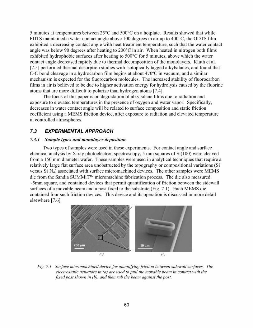
60
5 minutes at temperatures between 25°C and 500°C on a hotplate. Results showed that while FDTS maintained a water contact angle above 100 degrees in air up to 400°C, the ODTS film exhibited a decreasing contact angle with heat treatment temperature, such that the water contact angle was below 90 degrees after heating to 200°C in air. When heated in nitrogen both films exhibited hydrophobic surfaces after heating to 500°C for 5 minutes, above which the water contact angle decreased rapidly due to thermal decomposition of the monolayers. Kluth et al. [7.5] performed thermal desorption studies with isotopically tagged alkylsilanes, and found that C-C bond cleavage in a hydrocarbon film begins at about 470ºC in vacuum, and a similar mechanism is expected for the fluorocarbon molecules. The increased stability of fluorocarbon films in air is believed to be due to higher activation energy for hydrolysis caused by the fluorine atoms that are more difficult to polarize than hydrogen atoms [7.4].
The focus of this paper is on degradation of alkylsilane films due to radiation and exposure to elevated temperatures in the presence of oxygen and water vapor. Specifically, decreases in water contact angle will be related to surface composition and static friction coefficient using a MEMS friction device, after exposure to radiation and elevated temperature in controlled atmospheres. 7.3 EXPERIMENTAL APPROACH 7.3.1 Sample types and monolayer deposition
Two types of samples were used in these experiments. For contact angle and surface chemical analysis by X-ray photoelectron spectroscopy, 5 mm squares of Si(100) were cleaved from a 150 mm diameter wafer. These samples were used in analytical techniques that require a relatively large flat surface area unobstructed by the topography or compositional variations (Si versus Si3N4) associated with surface micromachined devices. The other samples were MEMS die from the Sandia SUMMiT micromachine fabrication process. The die also measured ~5mm square, and contained devices that permit quantification of friction between the sidewall surfaces of a movable beam and a post fixed to the substrate (Fig. 7.1). Each MEMS die contained four such friction devices. This device and its operation is discussed in more detail elsewhere [7.6].
Fig. 7.1. Surface micromachined device for quantifying friction between sidewall surfaces. The
electrostatic actuators in (a) are used to pull the movable beam in contact with the fixed post shown in (b), and then rub the beam against the post.
(a) (b)
200 µm 10 µm
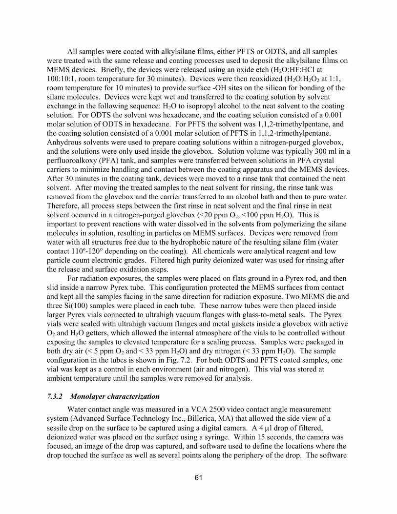
61
All samples were coated with alkylsilane films, either PFTS or ODTS, and all samples were treated with the same release and coating processes used to deposit the alkylsilane films on MEMS devices. Briefly, the devices were released using an oxide etch (H2O:HF:HCl at 100:10:1, room temperature for 30 minutes). Devices were then reoxidized (H2O:H2O2 at 1:1, room temperature for 10 minutes) to provide surface -OH sites on the silicon for bonding of the silane molecules. Devices were kept wet and transferred to the coating solution by solvent exchange in the following sequence: H2O to isopropyl alcohol to the neat solvent to the coating solution. For ODTS the solvent was hexadecane, and the coating solution consisted of a 0.001 molar solution of ODTS in hexadecane. For PFTS the solvent was 1,1,2-trimethylpentane, and the coating solution consisted of a 0.001 molar solution of PFTS in 1,1,2-trimethylpentane. Anhydrous solvents were used to prepare coating solutions within a nitrogen-purged glovebox, and the solutions were only used inside the glovebox. Solution volume was typically 300 ml in a perfluoroalkoxy (PFA) tank, and samples were transferred between solutions in PFA crystal carriers to minimize handling and contact between the coating apparatus and the MEMS devices. After 30 minutes in the coating tank, devices were moved to a rinse tank that contained the neat solvent. After moving the treated samples to the neat solvent for rinsing, the rinse tank was removed from the glovebox and the carrier transferred to an alcohol bath and then to pure water. Therefore, all process steps between the first rinse in neat solvent and the final rinse in neat solvent occurred in a nitrogen-purged glovebox (<20 ppm O2, <100 ppm H2O). This is important to prevent reactions with water dissolved in the solvents from polymerizing the silane molecules in solution, resulting in particles on MEMS surfaces. Devices were removed from water with all structures free due to the hydrophobic nature of the resulting silane film (water contact 110º-120° depending on the coating). All chemicals were analytical reagent and low particle count electronic grades. Filtered high purity deionized water was used for rinsing after the release and surface oxidation steps.
For radiation exposures, the samples were placed on flats ground in a Pyrex rod, and then slid inside a narrow Pyrex tube. This configuration protected the MEMS surfaces from contact and kept all the samples facing in the same direction for radiation exposure. Two MEMS die and three Si(100) samples were placed in each tube. These narrow tubes were then placed inside larger Pyrex vials connected to ultrahigh vacuum flanges with glass-to-metal seals. The Pyrex vials were sealed with ultrahigh vacuum flanges and metal gaskets inside a glovebox with active O2 and H2O getters, which allowed the internal atmosphere of the vials to be controlled without exposing the samples to elevated temperature for a sealing process. Samples were packaged in both dry air (< 5 ppm O2 and < 33 ppm H2O) and dry nitrogen (< 33 ppm H2O). The sample configuration in the tubes is shown in Fig. 7.2. For both ODTS and PFTS coated samples, one vial was kept as a control in each environment (air and nitrogen). This vial was stored at ambient temperature until the samples were removed for analysis.
7.3.2 Monolayer characterization
Water contact angle was measured in a VCA 2500 video contact angle measurement system (Advanced Surface Technology Inc., Billerica, MA) that allowed the side view of a sessile drop on the surface to be captured using a digital camera. A 4 µl drop of filtered, deionized water was placed on the surface using a syringe. Within 15 seconds, the camera was focused, an image of the drop was captured, and software used to define the locations where the drop touched the surface as well as several points along the periphery of the drop. The software
62
Fig. 7.2. MEMS die sitting on a flat ground in Pyrex rod, and this inside a Pyrex tube (a), and these components inside a vial for radiation and thermal exposure in controlled environments (b).
then calculated the contact angle on both sides of the drop. These two numbers were usually identical, but in some cases differed by up to 2 degrees. The average of the two numbers was recorded as the water contact angle for the sample. Two samples were measured for each experimental condition. This technique was used as a primary screening tool, to identify samples of interest for analysis using other techniques.
Surface chemical information was obtained using x-ray photoelectron spectroscopy (XPS). A PHI achromatic XPS system (Physical Electronics, Eden Prairie, MN) was used for analysis. Spectra were digitally acquired using an Al Kα x-ray source (1486.6 eV). A survey spectrum was collected on each sample, followed by detailed scans using analysis regions that captured the Si2p, C1s, O1s and F1s (for the PFTS) peaks. Si, O and F peaks were acquired at 0.2 eV/step, while C was acquired at 0.1 eV/step. After analysis, the spectra were smoothed using a 19-point Savitsky-Golay algorithm, satellite subtraction was performed, and the spectra were shifted to provide a constant Si2p3/2 peak position at 99.3 eV. Atomic concentrations were calculated from the detailed scans using handbook sensitivity factors. For comparison of peak shapes and offsets due to chemical changes in the films, the peaks for a given element were normalized by peak area and plotted with a baseline intensity offset to stagger the peaks.
7.3.3 Friction measurements
Static friction was determined using the MEMS devices shown in Figure 7.1. All measurements were conducted in laboratory ambient atmosphere (23°C, 13% relative humidity) using bare die and drive signals applied with probes making contact with electrical contact pads on the device. A DC voltage was applied to the loading actuator to bring the beam into contact with the post (Figure 7.1b). Normal load is estimated at 10 µN based on the applied voltage and displacement of the beam. With the load applied, the voltage on the oscillation actuator was slowly ramped up from zero while acquiring images of the beam via the probe station microscope. In this configuration, the beam remains stationary against the post until sufficient force is applied by the actuator to overcome the static friction between the beam and the post. At this point, the beam slips. Image processing was used to calculate the displacement of the beam as a function of voltage applied to the oscillation actuator. The force at which slip takes place can be calculated as described by Senft and Dugger [7.6], using the lateral stiffness of springs in
(a) (b)
63
the friction structure and the calibration parameters for displacement versus voltage of the actuators.
7.3.4 Description of radiation exposure facility
Samples were irradiated at the Gamma Irradiation Facility (GIF) at Sandia National Laboratories. The GIF radiation source consists of an array of stainless steel tubes packed with pellets of the radioactive isotope Co-60. Co-60 decays to Ni-60, emitting photons at 1.17 MeV and 1.33 MeV with equal frequency. The exposure time is controlled by raising the source from a water-filled well, in which it is stored, up into the test cell. Dose rate is determined by the proximity of the samples to the source.
Compton scattering of the Co-60 primary photons creates a field of low-energy photons in the test cell. At low photon energies, photon absorption varies strongly with atomic number and energy, making it difficult to deliver controlled and well-characterized doses to test samples. To circumvent this issue, the samples at GIF are placed in a Pb/Al box that absorbs most of the low-energy photons while allowing most of the Co-60 photons to pass through.
7.3.5 Radiation exposures
Irradiations were performed on eight sets of samples, each set packaged in a sealed tube. The samples covered a 2x2x2 test matrix, with the following splits: PFTS vs. ODTS coating, air vs. nitrogen atmosphere, and 50 vs. 500 krad total ionizing dose. The set of samples are summarized in Table 7.1.
Table 7.1: Matrix of samples for radiation exposures at GIF Atmosphere Coating Nominal Dose Dry Air Nitrogen
50 krad �ODTS-Air-A� �ODTS-N2-A� ODTS 500 krad �ODTS-Air-B� �ODTS-N2-B� 50 krad �#63� �#56� PFTS 500 krad �#52� �#60�
The exposures were performed at a dose rate of roughly 10 rad/s. All of the samples were
first subjected to a nominal exposure of 50 krad. Then half of the samples were removed and an additional exposure of 450 krad was performed to bring the remaining samples to a total dose of 500 krad.
7.3.6 Dose measurement
Radiation dose was measured using doped calcium fluoride (CaF2) thermoluminescent dosimeters (TLDs), which provide a calibrated (NIST traceable) measurement of total ionizing dose. For each irradiation, 4 TLDs were taped to the front of each tube. The photons generated by the GIF source are highly penetrating, and the TLDs and the Pyrex tubes should not significantly attenuate the radiation arriving at the samples.
At free surfaces or at interfaces between dissimilar materials, Compton and/or photoelectrons can be ejected from one material into the other, increasing the dose in the electron recipient and decreasing that in the donor. The range of these electrons is much shorter than that of the primary photons. A section of material that experiences no enhancement or reduction in dose due to the redistribution of electrons is said to be at equilibrium. To ensure accurate dose
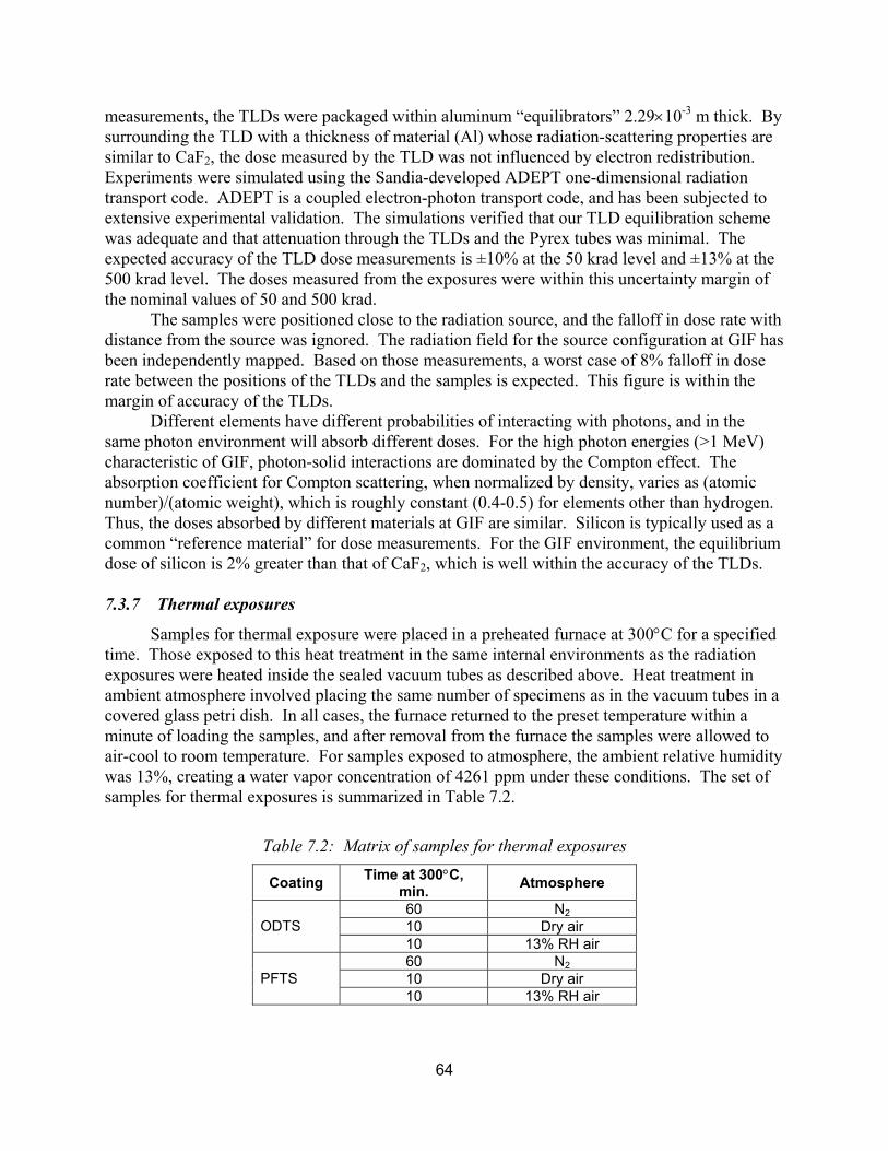
64
measurements, the TLDs were packaged within aluminum �equilibrators� 2.29×10⁻³ m thick. By surrounding the TLD with a thickness of material (Al) whose radiation-scattering properties are similar to CaF2, the dose measured by the TLD was not influenced by electron redistribution. Experiments were simulated using the Sandia-developed ADEPT one-dimensional radiation transport code. ADEPT is a coupled electron-photon transport code, and has been subjected to extensive experimental validation. The simulations verified that our TLD equilibration scheme was adequate and that attenuation through the TLDs and the Pyrex tubes was minimal. The expected accuracy of the TLD dose measurements is ±10% at the 50 krad level and ±13% at the 500 krad level. The doses measured from the exposures were within this uncertainty margin of the nominal values of 50 and 500 krad.
The samples were positioned close to the radiation source, and the falloff in dose rate with distance from the source was ignored. The radiation field for the source configuration at GIF has been independently mapped. Based on those measurements, a worst case of 8% falloff in dose rate between the positions of the TLDs and the samples is expected. This figure is within the margin of accuracy of the TLDs.
Different elements have different probabilities of interacting with photons, and in the same photon environment will absorb different doses. For the high photon energies (>1 MeV) characteristic of GIF, photon-solid interactions are dominated by the Compton effect. The absorption coefficient for Compton scattering, when normalized by density, varies as (atomic number)/(atomic weight), which is roughly constant (0.4-0.5) for elements other than hydrogen. Thus, the doses absorbed by different materials at GIF are similar. Silicon is typically used as a common �reference material� for dose measurements. For the GIF environment, the equilibrium dose of silicon is 2% greater than that of CaF2, which is well within the accuracy of the TLDs.
7.3.7 Thermal exposures
Samples for thermal exposure were placed in a preheated furnace at 300°C for a specified time. Those exposed to this heat treatment in the same internal environments as the radiation exposures were heated inside the sealed vacuum tubes as described above. Heat treatment in ambient atmosphere involved placing the same number of specimens as in the vacuum tubes in a covered glass petri dish. In all cases, the furnace returned to the preset temperature within a minute of loading the samples, and after removal from the furnace the samples were allowed to air-cool to room temperature. For samples exposed to atmosphere, the ambient relative humidity was 13%, creating a water vapor concentration of 4261 ppm under these conditions. The set of samples for thermal exposures is summarized in Table 7.2.
Table 7.2: Matrix of samples for thermal exposures
Coating Time at 300°C, min. Atmosphere
60 N2 10 Dry air ODTS 10 13% RH air 60 N2 10 Dry air PFTS 10 13% RH air
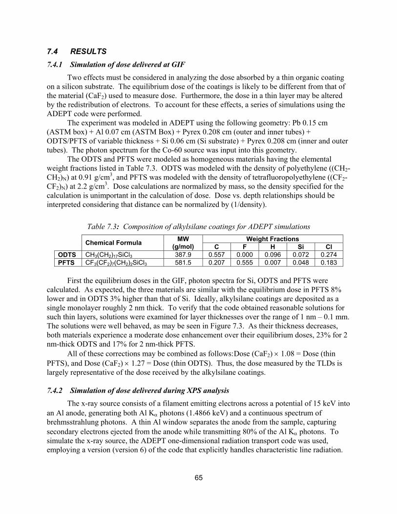
65
7.4 RESULTS 7.4.1 Simulation of dose delivered at GIF
Two effects must be considered in analyzing the dose absorbed by a thin organic coating on a silicon substrate. The equilibrium dose of the coatings is likely to be different from that of the material (CaF2) used to measure dose. Furthermore, the dose in a thin layer may be altered by the redistribution of electrons. To account for these effects, a series of simulations using the ADEPT code were performed.
The experiment was modeled in ADEPT using the following geometry: Pb 0.15 cm (ASTM box) + Al 0.07 cm (ASTM Box) + Pyrex 0.208 cm (outer and inner tubes) + ODTS/PFTS of variable thickness + Si 0.06 cm (Si substrate) + Pyrex 0.208 cm (inner and outer tubes). The photon spectrum for the Co-60 source was input into this geometry.
The ODTS and PFTS were modeled as homogeneous materials having the elemental weight fractions listed in Table 7.3. ODTS was modeled with the density of polyethylene ((CH2-CH2)N) at 0.91 g/cm3, and PFTS was modeled with the density of tetrafluoropolyethylene ((CF2-CF2)N) at 2.2 g/cm3. Dose calculations are normalized by mass, so the density specified for the calculation is unimportant in the calculation of dose. Dose vs. depth relationships should be interpreted considering that distance can be normalized by (1/density).
Table 7.3: Composition of alkylsilane coatings for ADEPT simulations Weight Fractions Chemical Formula MW
(g/mol) C F H Si Cl ODTS CH3(CH2)17SiCl3 387.9 0.557 0.000 0.096 0.072 0.274 PFTS CF3(CF2)7(CH2)2SiCl3 581.5 0.207 0.555 0.007 0.048 0.183
First the equilibrium doses in the GIF, photon spectra for Si, ODTS and PFTS were
calculated. As expected, the three materials are similar with the equilibrium dose in PFTS 8% lower and in ODTS 3% higher than that of Si. Ideally, alkylsilane coatings are deposited as a single monolayer roughly 2 nm thick. To verify that the code obtained reasonable solutions for such thin layers, solutions were examined for layer thicknesses over the range of 1 nm � 0.1 mm. The solutions were well behaved, as may be seen in Figure 7.3. As their thickness decreases, both materials experience a moderate dose enhancement over their equilibrium doses, 23% for 2 nm-thick ODTS and 17% for 2 nm-thick PFTS.
All of these corrections may be combined as follows: Dose (CaF2) × 1.08 = Dose (thin PFTS), and Dose (CaF2) × 1.27 = Dose (thin ODTS). Thus, the dose measured by the TLDs is largely representative of the dose received by the alkylsilane coatings.
7.4.2 Simulation of dose delivered during XPS analysis
The x-ray source consists of a filament emitting electrons across a potential of 15 keV into an Al anode, generating both Al Kα photons (1.4866 keV) and a continuous spectrum of brehmsstrahlung photons. A thin Al window separates the anode from the sample, capturing secondary electrons ejected from the anode while transmitting 80% of the Al Kα photons. To simulate the x-ray source, the ADEPT one-dimensional radiation transport code was used, employing a version (version 6) of the code that explicitly handles characteristic line radiation.
66
Fig. 7.3. Simulation results for thin ODTS (a) and PFTS (b) coatings at the GIF.
The spectrum emitted when a 15 keV electron impacts an aluminum target at normal incidence was first calculated. About 80% of the photons emitted are Al Kα with the remainder brehmsstrahlung. For the remainder of the analysis, the brehmsstrahlung radiation was neglected. The Al Kα yield is 2.64×10⁻³ photons per incident electron. The region within 13° of a normal to the surface contains about 24% of the total emitted photons per steradian. The tube runs at a maximum filament current of 30 mA, at which 4.95×10¹⁴ Al Kα photons/s will be emitted. Based upon the geometry and absorption in the Al window, the fluence of Al Kα photons on the sample is 2.3×10¹³ (s·cm2)-1.
Having estimated the fluence of Al Kα photons at the sample, an additional series of simulations were performed to estimate the ionizing dose in the alkylsilane coating. The simulation consisted of Al Kα photons impinging at normal incidence with a fluence of one photon/cm2 on a layer of ODTS/PFTS, of variable thickness, on a silicon substrate. As before, the thickness of the alkylsilane coating was varied over the range 1 nm to 0.1 mm, both to check that the solutions were well behaved at small thicknesses and to examine the variation of dose with film thickness.
Results of the simulations are plotted in Figure 7.4, which shows both kerma, the total energy transferred from the incident photons to electrons in the material, and dose, the energy deposited by those electrons, as a function of alkylsilane coating thickness. Both are given in units of MeV/g; note that 1 MeV/g = 1.602×10⁻¹⁰ rad. The figure plots the average dose/kerma in an alkylsilane coating of the specified thickness, and should not be interpreted as a dose-depth profile. The main difference between the geometry of the XPS experiments and that of the irradiations at GIF is that in the XPS there is no material in front of the sample to equilibrate it. Thus, electrons are free to escape from near-surface areas, reducing the dose in thin layers. Kerma, on the other hand, remains constant in thin layers, where it has values of 2.22 MeV/g and 1.05 MeV/g for PFTS and ODTS, respectively.
As the thickness of the alkylsilane layer increases, dose and kerma both drop exponentially as the primary photons are absorbed with a characteristic absorption length of roughly 4 mm in PFTS and 15 mm in ODTS. PFTS, which contains a fluorinated (Z=9) carbon chain, absorbs more strongly than ODTS, which contains a hydrogenated (Z=1) carbon chain. This is a sensible result, as the photoelectric cross section per atom varies as Z4.
1.00
1.05
1.10
1.15
1.20
1.25
0.1 1 10 100
ODTS Layer Thickness (nm)
Dos
e/(E
quili
briu
m D
ose)
1.00
1.05
1.10
1.15
1.20
1.25
0.1 1 10 100
PFTS Layer Thickness (nm)
Dos
e/(E
quili
briu
m D
ose)
(a) (b)
67
Fig. 7.4. Results of XPS dose simulations, assuming a fluence of 1 Al Kα photon per cm2.
Whether dose or kerma better represents the potential for damage to an alkylsilane coating is debatable. At low photon energies, the primary mechanism for photon interaction is the photoelectric effect, in which a photon is completely absorbed by an initially bound electron resulting in ionization. Dose represents the energy subsequently transferred by that electron to others, potentially resulting in multiple ionizations. Kerma is simpler to work with, as dose varies strongly with thickness for alkylsilane coatings less than 100 nm thick while kerma is constant over this range. Kerma will be used to estimate the potential damaging effects of Al Kα on alkylsilane coatings, considering that the use of dose instead of kerma would reduce the damage rates roughly 50% for a 2 nm film ODTS film and a factor of four for a PFTS film (see Figure 7.4).
If the kerma from Figure 7.4 in units of MeV/g per photon/s·cm2, is multiplied by the estimated photon fluence of 2.3×10¹³ photons/s·cm2, the dose rate in a thin alkylsilane coating during XPS analysis can be estimated. Converting from MeV/g to rad, the results are 380 krad/s for ODTS and 800 krad/s for PFTS. Even if these estimates are an order of magnitude too high, an XPS analysis lasting several minutes can clearly deposit megarads of dose into a thin coating.
7.4.3 Contact angle
Variation in water contact angle with exposure conditions for ODTS coatings is shown in Figure 7.5. The bars in the figure span the maximum and minimum contact angle observed, with the average value indicated by the symbol. The figure shows that the as-deposited ODTS exhibits a water contact angle of 110 degrees. There is no clear trend with irradiation dose, although the irradiated samples do exhibit contact angles as low as 105 degrees. However, this change is at the limits of significance considering the limited number of samples analyzed and the variation observed between samples. Contact angle variation for the thermal exposures reveals no effect of exposure for the dry air and nitrogen environments, regardless of exposure time. However, the samples exposed to a low concentration of water vapor during heating exhibited a dramatic decrease in contact angle.
0.0
0.5
1.0
1.5
2.0
2.5
1 10 100 1000 10000 100000Coating thickness (nm)
Dos
e (M
eV/g
)
ODTS DosePFTS DoseODTS KermaPFTS Kerma
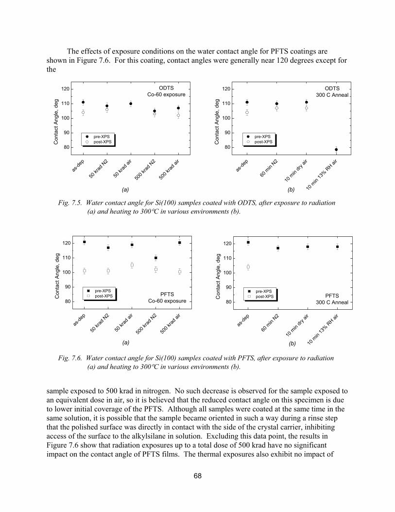
68
The effects of exposure conditions on the water contact angle for PFTS coatings are shown in Figure 7.6. For this coating, contact angles were generally near 120 degrees except for the
Fig. 7.5. Water contact angle for Si(100) samples coated with ODTS, after exposure to radiation (a) and heating to 300°C in various environments (b).
Fig. 7.6. Water contact angle for Si(100) samples coated with PFTS, after exposure to radiation (a) and heating to 300°C in various environments (b).
sample exposed to 500 krad in nitrogen. No such decrease is observed for the sample exposed to an equivalent dose in air, so it is believed that the reduced contact angle on this specimen is due to lower initial coverage of the PFTS. Although all samples were coated at the same time in the same solution, it is possible that the sample became oriented in such a way during a rinse step that the polished surface was directly in contact with the side of the crystal carrier, inhibiting access of the surface to the alkylsilane in solution. Excluding this data point, the results in Figure 7.6 show that radiation exposures up to a total dose of 500 krad have no significant impact on the contact angle of PFTS films. The thermal exposures also exhibit no impact of
as-de
p
50 kr
ad N
2
50 kr
ad ai
r
500 k
rad N
2
500 k
rad ai
r
80
90
100
110
120 ODTSCo-60 exposure
Con
tact
Ang
le, d
eg
pre-XPS post-XPS
(a)
as-de
p
60 m
in N2
10 m
in dry
air
10 m
in 13
% RH ai
r
80
90
100
110
120 ODTS300 C Anneal
Con
tact
Ang
le, d
eg
pre-XPS post-XPS
(b)
as-de
p
50 kr
ad N
2
50 kr
ad ai
r
500 k
rad N
2
500 k
rad ai
r
80
90
100
110
120
PFTSCo-60 exposure
Con
tact
Ang
le, d
eg
pre-XPS post-XPS
as-de
p
60 m
in N2
10 m
in dry
air
10 m
in 13
% RH ai
r
80
90
100
110
120
PFTS300 C Anneal
Con
tact
Ang
le, d
eg
pre-XPS post-XPS
(a) (b)
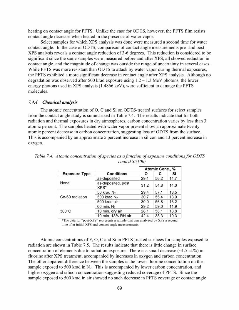
69
heating on contact angle for PFTS. Unlike the case for ODTS, however, the PFTS film resists contact angle decrease when heated in the presence of water vapor.
Select samples for which XPS analysis was done were measured a second time for water contact angle. In the case of ODTS, comparison of contact angle measurements pre- and post-XPS analysis reveals a contact angle reduction of 3-6 degrees. This reduction is considered to be significant since the same samples were measured before and after XPS, all showed reduction in contact angle, and the magnitude of change was outside the range of uncertainty in several cases. While PFTS was more resistant than ODTS to attack by water vapor during thermal exposures, the PFTS exhibited a more significant decrease in contact angle after XPS analysis. Although no degradation was observed after 500 krad exposure using 1.2 � 1.3 MeV photons, the lower energy photons used in XPS analysis (1.4866 keV), were sufficient to damage the PFTS molecules.
7.4.4 Chemical analysis
The atomic concentration of O, C and Si on ODTS-treated surfaces for select samples from the contact angle study is summarized in Table 7.4. The results indicate that for both radiation and thermal exposures in dry atmospheres, carbon concentration varies by less than 3 atomic percent. The samples heated with water vapor present show an approximate twenty atomic percent decrease in carbon concentration, suggesting loss of ODTS from the surface. This is accompanied by an approximate 5 percent increase in silicon and 13 percent increase in oxygen.
Table 7.4. Atomic concentration of species as a function of exposure conditions for ODTS coated Si(100)
Atomic Conc., % Exposure Type Conditions O C Si
as-deposited 29.1 56.2 14.7 None as-deposited, post
XPS* 31.2 54.8 14.0
50 krad N2 29.4 57.1 13.5 500 krad N2 30.7 55.4 13.9 Co-60 radiation 500 krad air 30.0 56.8 13.2 60 min. N2 29.2 59.0 11.9 10 min. dry air 28.1 58.1 13.8 300°C 10 min. 13% RH air 42.4 38.3 19.3
*The data for �post-XPS� represents a sample that was analyzed by XPS a second time after initial XPS and contact angle measurements.
Atomic concentrations of F, O, C and Si in PFTS-treated surfaces for samples exposed to
radiation are shown in Table 7.5. The results indicate that there is little change in surface concentration of elements due to radiation exposure. There is a small decrease (~1.5 at.%) in fluorine after XPS treatment, accompanied by increases in oxygen and carbon concentration. The other apparent difference between the samples is the lower fluorine concentration on the sample exposed to 500 krad in N2. This is accompanied by lower carbon concentration, and higher oxygen and silicon concentration suggesting reduced coverage of PFTS. Since the sample exposed to 500 krad in air showed no such decrease in PFTS coverage or contact angle
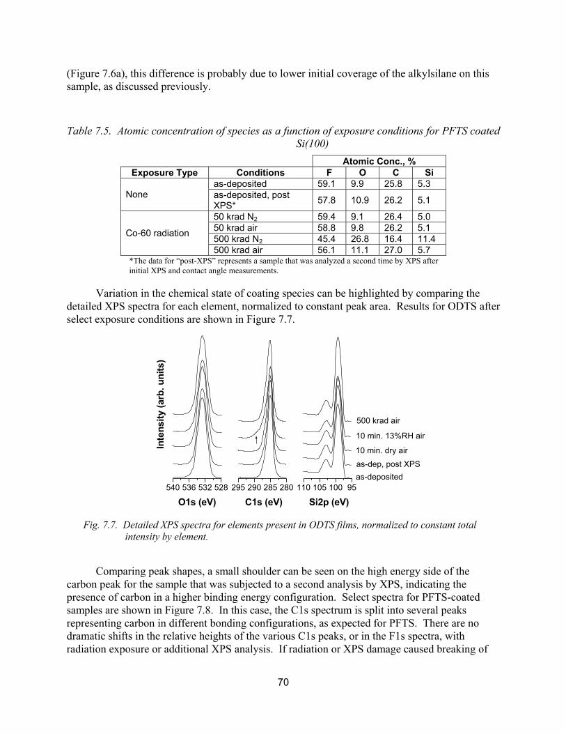
70
(Figure 7.6a), this difference is probably due to lower initial coverage of the alkylsilane on this sample, as discussed previously.
Table 7.5. Atomic concentration of species as a function of exposure conditions for PFTS coated Si(100)
Atomic Conc., % Exposure Type Conditions F O C Si
as-deposited 59.1 9.9 25.8 5.3 None as-deposited, post
XPS* 57.8 10.9 26.2 5.1
50 krad N2 59.4 9.1 26.4 5.0 50 krad air 58.8 9.8 26.2 5.1 500 krad N2 45.4 26.8 16.4 11.4 Co-60 radiation
500 krad air 56.1 11.1 27.0 5.7 *The data for �post-XPS� represents a sample that was analyzed a second time by XPS after initial XPS and contact angle measurements.
Variation in the chemical state of coating species can be highlighted by comparing the detailed XPS spectra for each element, normalized to constant peak area. Results for ODTS after select exposure conditions are shown in Figure 7.7.
Fig. 7.7. Detailed XPS spectra for elements present in ODTS films, normalized to constant total intensity by element.
Comparing peak shapes, a small shoulder can be seen on the high energy side of the carbon peak for the sample that was subjected to a second analysis by XPS, indicating the presence of carbon in a higher binding energy configuration. Select spectra for PFTS-coated samples are shown in Figure 7.8. In this case, the C1s spectrum is split into several peaks representing carbon in different bonding configurations, as expected for PFTS. There are no dramatic shifts in the relative heights of the various C1s peaks, or in the F1s spectra, with radiation exposure or additional XPS analysis. If radiation or XPS damage caused breaking of
540 536 532 528 295 290 285 280 110 105 100 95
Inte
nsity
(arb
. uni
ts)
O1s (eV) C1s (eV)
500 krad air
10 min. 13%RH air
10 min. dry airas-dep, post XPSas-deposited
Si2p (eV)
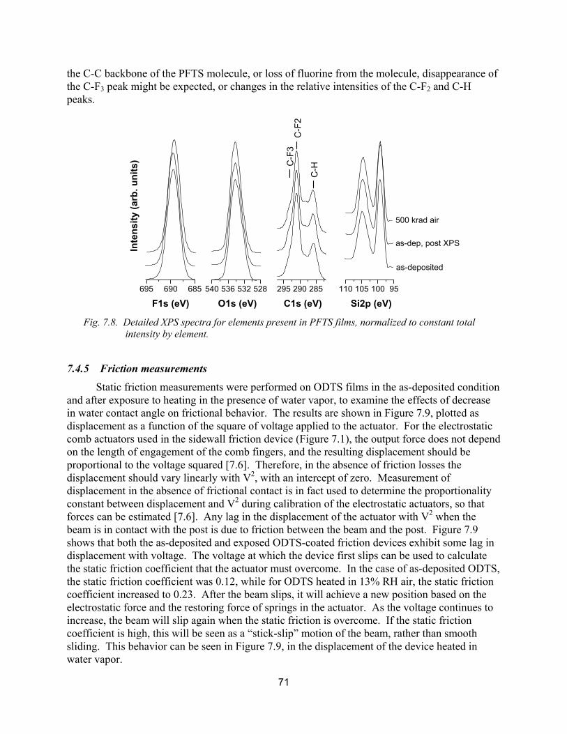
71
the C-C backbone of the PFTS molecule, or loss of fluorine from the molecule, disappearance of the C-F3 peak might be expected, or changes in the relative intensities of the C-F2 and C-H peaks.
Fig. 7.8. Detailed XPS spectra for elements present in PFTS films, normalized to constant total intensity by element.
7.4.5 Friction measurements
Static friction measurements were performed on ODTS films in the as-deposited condition and after exposure to heating in the presence of water vapor, to examine the effects of decrease in water contact angle on frictional behavior. The results are shown in Figure 7.9, plotted as displacement as a function of the square of voltage applied to the actuator. For the electrostatic comb actuators used in the sidewall friction device (Figure 7.1), the output force does not depend on the length of engagement of the comb fingers, and the resulting displacement should be proportional to the voltage squared [7.6]. Therefore, in the absence of friction losses the displacement should vary linearly with V2, with an intercept of zero. Measurement of displacement in the absence of frictional contact is in fact used to determine the proportionality constant between displacement and V2 during calibration of the electrostatic actuators, so that forces can be estimated [7.6]. Any lag in the displacement of the actuator with V2 when the beam is in contact with the post is due to friction between the beam and the post. Figure 7.9 shows that both the as-deposited and exposed ODTS-coated friction devices exhibit some lag in displacement with voltage. The voltage at which the device first slips can be used to calculate the static friction coefficient that the actuator must overcome. In the case of as-deposited ODTS, the static friction coefficient was 0.12, while for ODTS heated in 13% RH air, the static friction coefficient increased to 0.23. After the beam slips, it will achieve a new position based on the electrostatic force and the restoring force of springs in the actuator. As the voltage continues to increase, the beam will slip again when the static friction is overcome. If the static friction coefficient is high, this will be seen as a �stick-slip� motion of the beam, rather than smooth sliding. This behavior can be seen in Figure 7.9, in the displacement of the device heated in water vapor.
695 690 685 540 536 532 528 295 290 285 110 105 100 95
C-H
Inte
nsity
(arb
. uni
ts)
F1s (eV) O1s (eV)C
-F3
C-F
2 C1s (eV)
500 krad air
as-dep, post XPS
as-deposited
Si2p (eV)
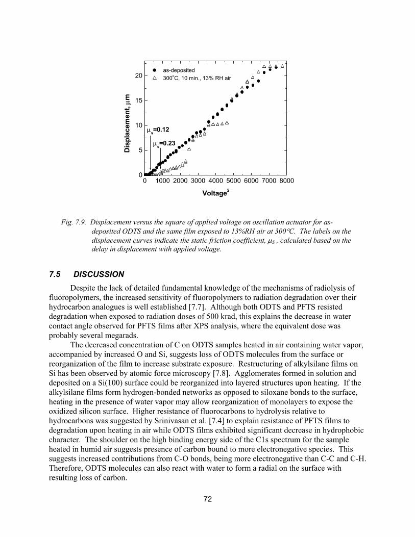
72
Fig. 7.9. Displacement versus the square of applied voltage on oscillation actuator for as-deposited ODTS and the same film exposed to 13%RH air at 300°C. The labels on the displacement curves indicate the static friction coefficient, µS , calculated based on the delay in displacement with applied voltage.
7.5 DISCUSSION Despite the lack of detailed fundamental knowledge of the mechanisms of radiolysis of
fluoropolymers, the increased sensitivity of fluoropolymers to radiation degradation over their hydrocarbon analogues is well established [7.7]. Although both ODTS and PFTS resisted degradation when exposed to radiation doses of 500 krad, this explains the decrease in water contact angle observed for PFTS films after XPS analysis, where the equivalent dose was probably several megarads.
The decreased concentration of C on ODTS samples heated in air containing water vapor, accompanied by increased O and Si, suggests loss of ODTS molecules from the surface or reorganization of the film to increase substrate exposure. Restructuring of alkylsilane films on Si has been observed by atomic force microscopy [7.8]. Agglomerates formed in solution and deposited on a Si(100) surface could be reorganized into layered structures upon heating. If the alkylsilane films form hydrogen-bonded networks as opposed to siloxane bonds to the surface, heating in the presence of water vapor may allow reorganization of monolayers to expose the oxidized silicon surface. Higher resistance of fluorocarbons to hydrolysis relative to hydrocarbons was suggested by Srinivasan et al. [7.4] to explain resistance of PFTS films to degradation upon heating in air while ODTS films exhibited significant decrease in hydrophobic character. The shoulder on the high binding energy side of the C1s spectrum for the sample heated in humid air suggests presence of carbon bound to more electronegative species. This suggests increased contributions from C-O bonds, being more electronegative than C-C and C-H. Therefore, ODTS molecules can also react with water to form a radial on the surface with resulting loss of carbon.
0 1000 2000 3000 4000 5000 6000 7000 80000
5
10
15
20
µs=0.23
µs=0.12
as-deposited 300oC, 10 min., 13% RH air
Dis
plac
emen
t, µm
Voltage2
73
The increase in static friction for the ODTS sample heated in the presence of water vapor, measured using a MEMS device operating in air, shows that degradation of hydrophobicity for alkylsilane films can result in increased friction coefficient. Since the devices were operated in air, hydrophilic surfaces facilitate adsorption of water and meniscus formation at the asperity contacts. This increases capillary adhesion between the beam and the post. Capillary films can increase the normal contact force between the beam and post, and must also be sheared in order to slide the beam tangentially. Both effects result in an increase in the force necessary to move the beam, and thus an increase in the static friction coefficient.
7.6 CONCLUSIONS
ODTS and PFTS films on Si(100) and polycrystalline silicon MEMS devices have been exposed to radiation and thermal treatments in controlled environments. Neither film exhibited a decrease in hydrophobic character upon exposure to a dose of 500 krad from Co-60 radiation. However, PFTS films on Si(100) exhibited degradation after XPS analysis, where the equivalent dose was estimated to be several megarads.
Although the radiation dose estimated for the samples during XPS analysis seems very high, it is important to note that the lower energy photons result in significant dose enhancement due to production of photoelectrons in the near surface of the samples. Therefore, modest x-ray exposure of devices could result in significant doses at surfaces treated with alkylsilanes, potentially resulting in degradation of the films. Due to their increased sensitivity to radiolysis, fluorinated alkylsilane films would be expected to undergo more degradation than hydrocarbon films in radiation environments.
ODTS films heated in air containing 4261 ppm water vapor exhibited significant decrease in water contact angle. This is in agreement with previous work showing increased degradation of ODTS in air compared to PFTS [7.4], although the water vapor concentration in the previous work was not reported. XPS analysis suggests that this degradation is accompanied by an increase in contributions to the C1s spectrum from C-O bonds. Hydrolysis of the ODTS molecule results in loss of carbon from the treated surface. Although water vapor can clearly cause degradation of ODTS films, this work has shown that heating for up to 60 minutes in nitrogen, and for 10 minutes in air containing less than 33 ppm H2O, caused no measurable changes in hydrophobicity of ODTS films. The PFTS films resisted degradation during heating in all of these environments.
Changes in static friction coefficient for ODTS heated in water vapor were significant. The static friction coefficient increased by a factor of two compared to the as-deposited film. Such changes in the friction force that must be overcome to move MEMS structures could have significant impact on the reliability of devices exposed to elevated temperature in the presence of water vapor. Additional work is needed to investigate the effects of lower concentrations of H2O on hydrolysis of ODTS, and the kinetics of degradation in low water vapor atmospheres.
7.7 ACKNOWLEDGEMENTS
The authors wish to thank Frere MacNamara in the Materials Characterization department for performing the XPS analyses, and Liz Sorroche in the Microsystem Materials, Tribology and Technology department for assistance with fixturing to control the atmosphere during irradiation and thermal treatment. The authors also acknowledge the help of Specialty Glass Co., Albuquerque, NM. Sandia is a multiprogram laboratory operated by Sandia Corporation, a
74
Lockheed Martin Company, for the United States Department of Energy under contract DE-AC04-94AL85000.
7.8 REFERENCES
7.1 C.H. Mastrangelo, �Adhesion Related Failure Mechanisms in Micromechanical Devices�,
Tribology Letters 3, pp. 223-238, 1997. 7.2 R. Maboudian, W. R. Ashurst and C. Carraro, �Self-Assembled Monolayers as Anti-
Stiction Coatings for MEMS: Characteristics and Recent Developments�, Sensors and Actuators A 82, pp. 219-223, (2000).
7.3 U. Srinivasan, J.D. Foster, U. Habib, R.T. Howe, R. Maboudian, D.C. Senft and M.T. Dugger, �Lubrication Of Polysilicon Micromechanisms With Self-Assembled Monolayers,� Technical Digest Solid-State Sensor and Actuator Workshop, 8-11 June 1998, Hilton Head Island, SC, USA, pp.156-61, Transducer Res. Found.: Cleveland, OH, 1998 .
7.4 U. Srinivasan, M.R. Houston, R.T. Howe, and R. Maboudian, �Alkyltrichlorosilane-Based Self-Assembled Monolayer Films for Stiction Reduction in Silicon Micromachines� J. Microelectromechanical Systems 7, pp. 252-260, 1998.
7.5 G.J. Kluth, M. Sander, M.M. Sung and R. Maboudian, �Study of the Desorption Mechanism of Alkylsiloxane Self-Assembled Monolayers Through Isotopic Labeling and High Resolution Electron Energy-Loss Spectroscopy Experiments,� J. Vacuum Sci. and Technol. A16, pp. 932-936, 1998.
7.6 D.C. Senft and M.T. Dugger, �Friction and Wear in Surface Micromachined Tribological Test Devices�, Proc. of the SPIE - The International Society for Optical Engineering 3224, pp. 31-38, 1997.
7.7 J.S. Forsythe and D.J. T. Hill, �The Radiation Chemistry of Fluoropolymers,� Prog. Polym. Sci. 25, pp. 101-136, 2000.
7.8 B.C. Bunker, R. W. Carpick, R.A. Assink, M.L. Thomas, M.G. Hankins, J.A. Voigt, D. Sipola, M.P. deBoer and G.L. Gulley, �The Impact of Solution Agglomeration on the Deposition of Self-Assembled Monolayers,� Langmuir 16, pp. 7742-7751, 2000.
75
8 Friction and Wear of Selective Tungsten Coatings for Surface Micromachined Silicon Devices
8.1 Introduction
Wear of silicon surfaces in microelectromechanical devices limits their use in applications requiring long life. Several surface modification strategies have been explored for reducing friction and wear in MEMS devices, including adsorbed organic molecules [8.1, 8.2], hard coatings and solid lubricants [8.2], and films deposited by atomic layer deposition [8.3]. Selective tungsten has also been examined to treat surfaces of silicon MEMS devices [8.4], and has the advantage that the basic process was developed in the 1980�s and is well understood, semiconductor fabrication equipment exists to deposit the coatings, and this process is compatible with most CMOS fabrication facilities. Prior work has focused on the deposition process for the coating applied to microsystems, adhesion and basic device functionality measurements determined from treated MEMS devices [8.4]. The purpose of this study was to examine the surface composition of selective tungsten films as a function of age after deposition, quantify the friction performance of this treatment in a MEMS sliding contact, and identify the surface species responsible for the observed friction and wear performance.
8.2 Experimental Approach 8.2.1 Treatment of SMM devices with selective tungsten
Tungsten is deposted on silicon device surfaces using chemical vapor deposition. A WF6 plasma is used, and silicon at the surface is replaced by tungsten according to one of the following reactions.
2WF6 + 3Si ↔ 2W+ 3SiF4 ↑ WF6 + 3Si ↔ W+ 3SiF2 ↑
The reaction that proceeds is a function of the reaction temperatere where processing takes place. In order for the WF6 to react with the silicon surface, the silicon must be clean and free of any residual oxide. In order to develop structures for friction and wear measurements, silicon SUMMiTTM die were first released in HF:HCl, rinsed in water and then dried using supercritical CO2. This allows the silicon structural elements to be exposed from the sacrificial oxide with no surface treatment applied and without having structures collapse under meniscus forces during drying of the devices. Although this process results in a nominally uncoated surface, there are residual organic contaminants present from the CO2 process, and a natural oxide also forms during the post-release rinse and any time spent exposed to air. These materials must be removed prior to the selective tungsten process, since the reactions shown above will only proceed in the presence of clean silicon surface.
8.2.2 Surface Chemical Analysis
Surface chemical information was obtained using x-ray photoelectron spectroscopy (XPS). A PHI achromatic XPS system (Physical Electronics, Eden Prairie, MN) was used for analysis. Spectra were digitally acquired using an Al Kα x-ray source (1486.6 eV). A survey spectrum was collected on each sample, followed by detailed scans using analysis regions that
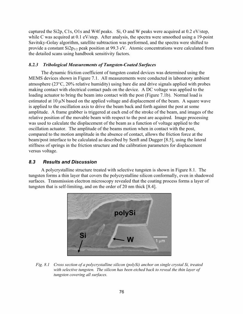
76
captured the Si2p, C1s, O1s and W4f peaks. Si, O and W peaks were acquired at 0.2 eV/step, while C was acquired at 0.1 eV/step. After analysis, the spectra were smoothed using a 19-point Savitsky-Golay algorithm, satellite subtraction was performed, and the spectra were shifted to provide a constant Si2p3/2 peak position at 99.3 eV. Atomic concentrations were calculated from the detailed scans using handbook sensitivity factors.
8.2.3 Tribological Measurements of Tungsten-Coated Surfaces
The dynamic friction coefficient of tungsten coated devices was determined using the MEMS devices shown in Figure 7.1. All measurements were conducted in laboratory ambient atmosphere (23°C, 20% relative humidity) using bare die and drive signals applied with probes making contact with electrical contact pads on the device. A DC voltage was applied to the loading actuator to bring the beam into contact with the post (Figure 7.1b). Normal load is estimated at 10 µN based on the applied voltage and displacement of the beam. A square wave is applied to the oscillation axis to drive the beam back and forth against the post at some amplitude. A frame grabber is triggered at each end of the stroke of the beam, and images of the relative position of the movable beam with respect to the post are acquired. Image processing was used to calculate the displacement of the beam as a function of voltage applied to the oscillation actuator. The amplitude of the beams motion when in contact with the post, compared to the motion amplitude in the absence of contact, allows the friction force at the beam/post interface to be calculated as described by Senft and Dugger [8.5], using the lateral stiffness of springs in the friction structure and the calibration parameters for displacement versus voltage.
8.3 Results and Discussion
A polycrystalline structure treated with selective tungsten is shown in Figure 8.1. The tungsten forms a thin layer that covers the polycrystalline silicon conformally, even in shadowed surfaces. Transmission electron microscopy revealed that the coating process forms a layer of tungsten that is self-limiting, and on the order of 20 nm thick [8.4].
Fig. 8.1 Cross section of a polycrystalline silicon (polySi) anchor on single crystal Si, treated
with selective tungsten. The silicon has been etched back to reveal the thin layer of tungsten covering all surfaces.
1 µm1 µm
polySi
WSi
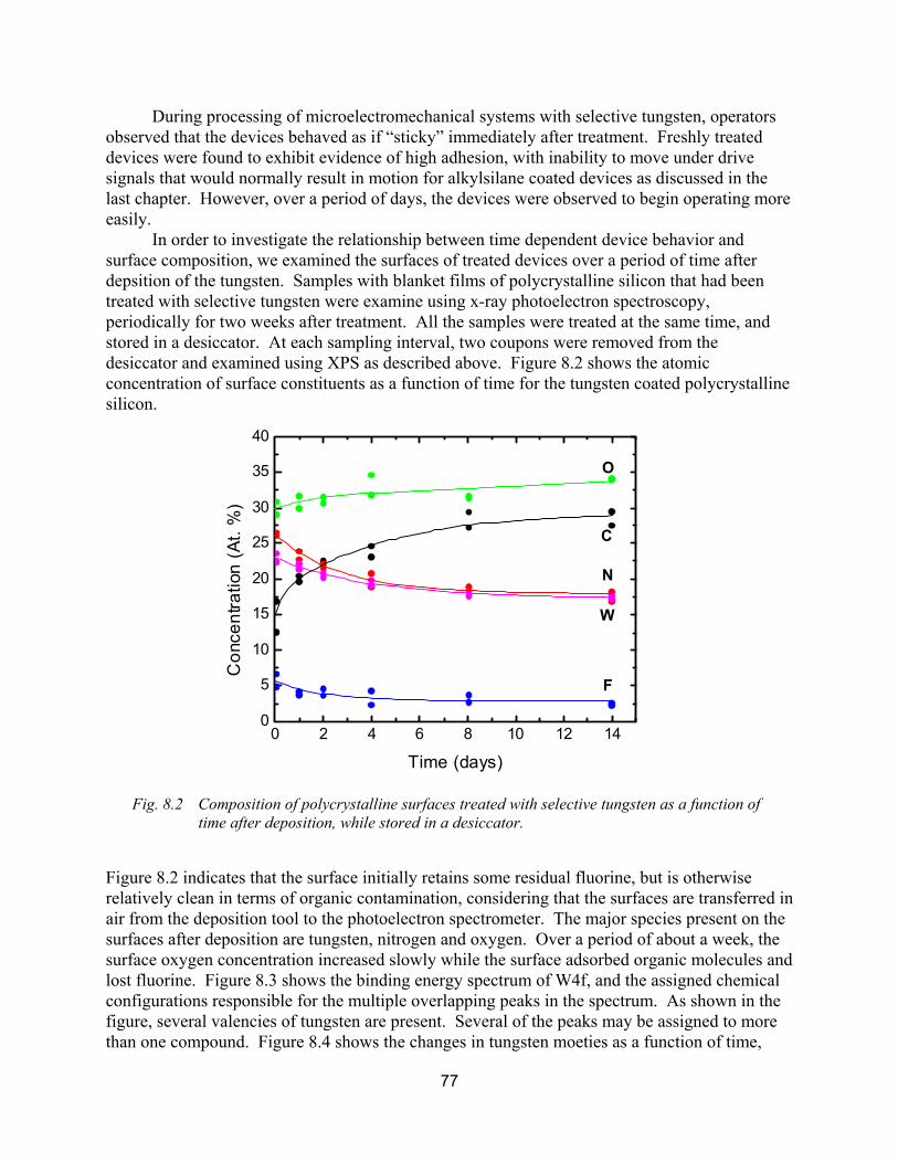
77
During processing of microelectromechanical systems with selective tungsten, operators observed that the devices behaved as if �sticky� immediately after treatment. Freshly treated devices were found to exhibit evidence of high adhesion, with inability to move under drive signals that would normally result in motion for alkylsilane coated devices as discussed in the last chapter. However, over a period of days, the devices were observed to begin operating more easily.
In order to investigate the relationship between time dependent device behavior and surface composition, we examined the surfaces of treated devices over a period of time after depsition of the tungsten. Samples with blanket films of polycrystalline silicon that had been treated with selective tungsten were examine using x-ray photoelectron spectroscopy, periodically for two weeks after treatment. All the samples were treated at the same time, and stored in a desiccator. At each sampling interval, two coupons were removed from the desiccator and examined using XPS as described above. Figure 8.2 shows the atomic concentration of surface constituents as a function of time for the tungsten coated polycrystalline silicon.
Fig. 8.2 Composition of polycrystalline surfaces treated with selective tungsten as a function of
time after deposition, while stored in a desiccator.
Figure 8.2 indicates that the surface initially retains some residual fluorine, but is otherwise relatively clean in terms of organic contamination, considering that the surfaces are transferred in air from the deposition tool to the photoelectron spectrometer. The major species present on the surfaces after deposition are tungsten, nitrogen and oxygen. Over a period of about a week, the surface oxygen concentration increased slowly while the surface adsorbed organic molecules and lost fluorine. Figure 8.3 shows the binding energy spectrum of W4f, and the assigned chemical configurations responsible for the multiple overlapping peaks in the spectrum. As shown in the figure, several valencies of tungsten are present. Several of the peaks may be assigned to more than one compound. Figure 8.4 shows the changes in tungsten moeties as a function of time,
0 2 4 6 8 10 12 140
5
10
15
20
25
30
35
40
O
C
N
W
F
Con
cent
ratio
n (A
t. %
)
Time (days)
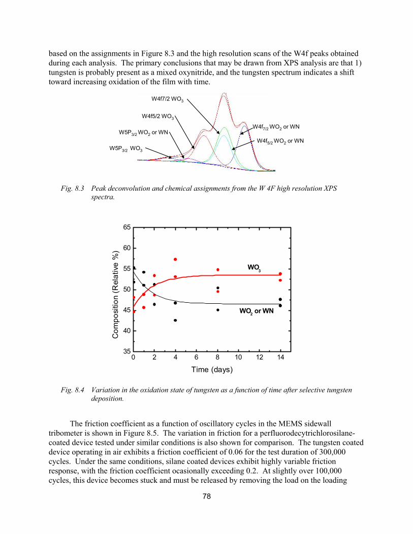
78
based on the assignments in Figure 8.3 and the high resolution scans of the W4f peaks obtained during each analysis. The primary conclusions that may be drawn from XPS analysis are that 1) tungsten is probably present as a mixed oxynitride, and the tungsten spectrum indicates a shift toward increasing oxidation of the film with time.
Fig. 8.3 Peak deconvolution and chemical assignments from the W 4F high resolution XPS
spectra.
Fig. 8.4 Variation in the oxidation state of tungsten as a function of time after selective tungsten
deposition.
The friction coefficient as a function of oscillatory cycles in the MEMS sidewall tribometer is shown in Figure 8.5. The variation in friction for a perfluorodecytrichlorosilane-coated device tested under similar conditions is also shown for comparison. The tungsten coated device operating in air exhibits a friction coefficient of 0.06 for the test duration of 300,000 cycles. Under the same conditions, silane coated devices exhibit highly variable friction response, with the friction coefficient ocasionally exceeding 0.2. At slightly over 100,000 cycles, this device becomes stuck and must be released by removing the load on the loading
W4f7/2 WO2 or WN
W4f5/2 WO2 or WNW5P3/2 WO2 or WN
W4f7/2 WO3
W4f5/2 WO3
W5P3/2 WO3
0 2 4 6 8 10 12 1435
40
45
50
55
60
65
WO2 or WN
WO3
Com
posi
tion
(Rel
ativ
e %
)
Time (days)
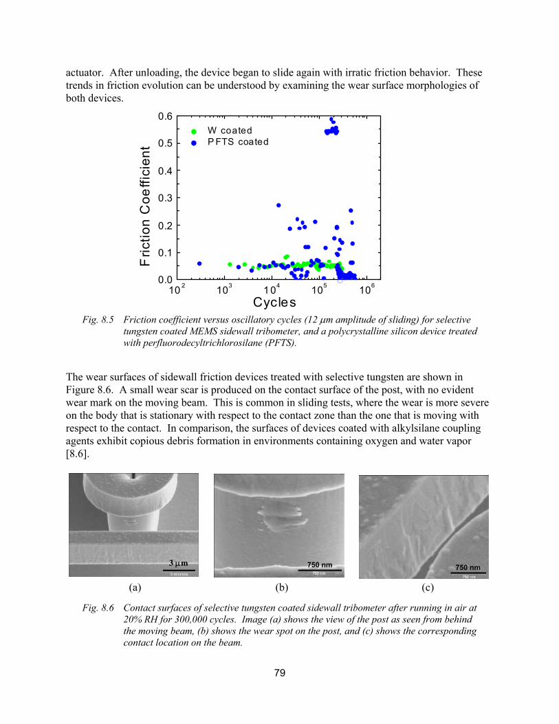
79
actuator. After unloading, the device began to slide again with irratic friction behavior. These trends in friction evolution can be understood by examining the wear surface morphologies of both devices.
Fig. 8.5 Friction coefficient versus oscillatory cycles (12 µm amplitude of sliding) for selective tungsten coated MEMS sidewall tribometer, and a polycrystalline silicon device treated with perfluorodecyltrichlorosilane (PFTS).
The wear surfaces of sidewall friction devices treated with selective tungsten are shown in Figure 8.6. A small wear scar is produced on the contact surface of the post, with no evident wear mark on the moving beam. This is common in sliding tests, where the wear is more severe on the body that is stationary with respect to the contact zone than the one that is moving with respect to the contact. In comparison, the surfaces of devices coated with alkylsilane coupling agents exhibit copious debris formation in environments containing oxygen and water vapor [8.6].
Fig. 8.6 Contact surfaces of selective tungsten coated sidewall tribometer after running in air at 20% RH for 300,000 cycles. Image (a) shows the view of the post as seen from behind the moving beam, (b) shows the wear spot on the post, and (c) shows the corresponding contact location on the beam.
10 2 103 104 105 1060.0
0.1
0.2
0.3
0.4
0.5
0.6 W coated P FTS coated
Fric
tion
Coe
ffici
ent
Cycles
3 µm 750 nm 750 nm
(a) (b) (c)
80
8.4 Conclusions Selective tungsten has been evaluated for use in sliding contacts in MEMS devices. The
surface was found to consist of a mixed tungsten oxide-nitride immediately after deposition, which continues to oxidize over a period of about one week when exposed to dry air. The behavior of this coating in a sliding contact was examined using a MEMS sidewall tribometer. The friction coefficient was found to be below 0.1 for at least 100,000 cycles of contact, with very little debris generation due to wear. The improved friction and wear behavior compared to polycrystalline surfaces treated with alkylsilane monolayer lubricants is believed to be due to the combination of wear resistance from a fine-grained tungsten oxide at the sliding surfaces, and lubrication provided by organic contamination adsorbed on the clean tungsten oxide surface. Selective tungsten shows promise as a surface treatment for silicon MEMS, since it is conformal, self-limiting, and thin enough that residual stress effects are not evident in 2 µm thick compliant structures. The film is also selective, in that reaction with a WF6 plasma will proceed only on clean silicon surfaces. Combined with controlled passivation, using for example hydrocarbon or fluorocarbon molecules as used on oxidized silicon surfaces, this treatment may provide both a wear resistant surface that is chemically stable and exhibits a low friction coefficient. Walraven et. al [8.4] found that the tensile strength of polycrystalline silicon was reduced significantly by preferrential reaction of the plasma species with grain boundary regions, creating �wormholes� at interface between the tungsten coating and the underlying silicon. For application to sliding surfaces without negative impact on strength, the process would have to be modified to prevent wormhole formation, or the structures designed for the lower tensile strength resulting on coated parts.
8.5 References 8.1 R. Maboudian, W.R. Ashurst and C. Carraro, �Tribological challenges in micromechanical
systems, � Tribology Letters 12 (2002) p. 95-100. 8.2 S.A. Henck, �Lubrication of digital micromirror devices,� Tribology Letters 3 (1997) p.
239-247. 8.3 T.M. Mayer, J.W. Elam, S.M. George, P.G. Kotula and R.S. Goeke, �Atomic-layer
deposition of wear-resistant coatings for microelectromechanical devices,� Applied Physics Letters 82 (2003) p. 2883-2885.
8.4 J.A. Walraven, S.S Mani, J.G. Fleming, T.J. Headley, P.G. Kotula, A.A. Pimentel, M.J. Rye, D.M. Tanner and N.F. Smith, Proceedings of the SPIE - The International Society for Optical Engineering 4180 (2000) p.49-57.
8.5 D.C. Senft and M.T. Dugger, �Friction and Wear in Surface Micromachined Tribological Test Devices�, Proc. of the SPIE - The International Society for Optical Engineering 3224 (1997), pp. 31-38.
8.6 M.T. Dugger, D.C. Senft and G.C. Nelson, "Friction and Durability of Chemisorbed Organic Lubricants for MEMS," in Microstructure and Tribology of Polymer Surfaces, V.V. Tsukruk and K.J. Wahl, eds., American Chemical Society, Washington, DC, 1999, pp. 455-473.
81
9 Conclusions and Recommendations
The Weibull strength distribution of SMM polysilicon was evaluated for each of the five structural silicon layers in the SUMMiTTM process over a wide range of stressed surface areas (200 to 20,000 µm2), thereby revealing the previously elusive Weibull size effect, as well as a strong layer-dependence. The layer dependence, thought to be at least partially due to microstructural variations, was consistent with a recently developed polycrystal elasticity model based on EBSD orientation maps of SUMMiTTM crystallography. New techniques were developed and applied to characterize the role of temperature and process steps (i.e. sacox cuts) on the observed strength behavior. Finally, a next generation of MEMS test structures, including compact tension fracture toughness structures and bend structures were fabricated and evaluated.
Surface micromachined (SMM) structures that contain isolated tribological contacts have been used to investigate interface performance of alkylsilane monolayers after storage in inert environments, and after exposure to a variety of thermal and radiation environments. Results show that both octadecyltrichlorosilane (ODTS) and perfluorodecyltrichlorosilane (PFTS) exhibit little change in hydrophobicity or friction after Co-60 radiation exposures at a total dose of up to 500 krad. However, exposure to temperature cycles consistent with packaging technologies, in the presence of low levels of water vapor, produces degradation of hydrophobicity and increase in static friction for ODTS films while producing no significant degradation in PFTS films. In addition, a range of new friction measurement tools for SMM structures have been developed. These include devices that permit a wider range of applied forces to be generated between contacting surfaces, and structures where the contacts may be latched into position to retain load without application of power. The latter are important structures for examining the effects of aging on the interface behavior of contacts under load.
New methodologies have been developed to study wear and subsurface deformation in electroplated metals for microsystems (LIGA). The methodology involves the application of focused ion beam (FIB) techniques to prepare cross sections of wear tracks. Electron backscatter diffraction (EBSD) analysis of wear scars on electroformed Ni revealed the formation two subsurface zones, each with its own characteristic features which are different from that of the bulk microstructure. Bending of columns in the direction of sliding, breakdown of columnar grains into equiaxed fine grain structure, and formation of low angle grain boundaries have been revealed. Formation of low-angle grain boundaries and spread in the orientation of pole figures were also observed. This work has demonstrated that focused ion beam techniques are ideally suited for preparing cross sections of shallow wear scars generated under low loads.
We have demonstrated the feasibility of characterizing adhesion between electroplated LIGA materials using a commercial MTS Nanoindenter XP with a LIGA fabricated adhesion probe tip in place of the standard Berkovich diamond indenter. It is well recognized that under the action of surface forces, the surfaces are drawn together and a finite area of contact is established for zero applied load. If an external load is applied, the contact area increases but on reducing the load it decreases reversibly. When the applied external load is removed, an additional load or a pull-off force is required to fully separate the two surfaces. Two widely referred models, the Johnson-Kendall-Roberts (JKR) model and the Derjaguin-Muller-Toporov (DMR) model, account for small but finite contact area at zero applied load in the presence of surface forces. In our measurements, the nanoindenter was programmed to collect data in the negative load regime until the surfaces were completely separated. LIGA Ni probe tips with a

82
variety of radii of curvature were fabricated and pressed into contact with a metallographically polished LIGA Ni disk. Load-displacement curves for these experiments showed negative loads in the unloading segments. This negative load or pull-off force allows us to quantify the adhesion forces between surfaces after removal of the applied load.
Alkylsilane monolayers were found to degrade upon exposure to water vapor at elevated temperatures, but not for exposures of up to an hour to elevated temperature in dry conditions.
Selective tungsten appears to be an attractive surface treatment option for MEMS with sliding surfaces. Controlled passivation of tungsten-coated surfaces may allow creation of wear resistant, low friction, and chemically stable surfaces. Strength reduction due to wormhole formation would require process modification, or structures designed to accommodate the lower tensile strength.
83
10 Distribution 3 MS 0889 M.T. Dugger, 1851 3 0889 T.E. Buchheit, 1851 3 0889 B.L. Boyce, 1851 3 0889 S.V. Prasad, 1851 1 0889 J.S. Custer, 1851 1 1084 P.J. Clews, 1746 1 1084 M.G. Hankins, 1746 1 1310 D. Tanner, 1762 1 1310 M.P. DeBoer, 1762 1 9401 J.J. Kelly, 8753 1 1425 W.G. Yelton, 1743 1 0188 LDRD Office, 1030 1 9018 Central Technical Files, 8945-1 2 0899 Technical Library, 9616