Linear Control Systems Engineering 线性控制系统工程
31
Linear Control Systems E ngineering 线线线线线 线线 统 Module 20 Phase Lag an d Lead- Lag Compen sation
-
Upload
nigel-berry -
Category
Documents
-
view
304 -
download
0
description
Linear Control Systems Engineering 线性控制系统工程. Module 20 Phase Lag and Lead- Lag Compensation ( 相位滞后和滞后 - 超前校正 ). Module 20 Phase Lag and Lead- Lag Compensation. -1/ τ. -1/ βτ. ▽ Transfer Function of Phase Lag Element. Phase lag networks. 1/ . 1/ . - PowerPoint PPT Presentation
Transcript of Linear Control Systems Engineering 线性控制系统工程
Linear Control Systems Engineering
线性控制系统工程
Module 20
Phase Lag and Lead- Lag Compensation
(相位滞后和滞后 -超前校正 )
Module 20 Phase Lag and Lead- Lag Compensation
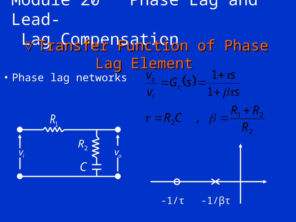
▽▽Transfer Function of Phase Lag ElementTransfer Function of Phase Lag Element
• Phase lag networks
-1/βτ-1/τ
2
212 ,
1
1
R
RRCR
s
ssG
v
vc
i
o
1R
Civ ov
2R
11
2
2
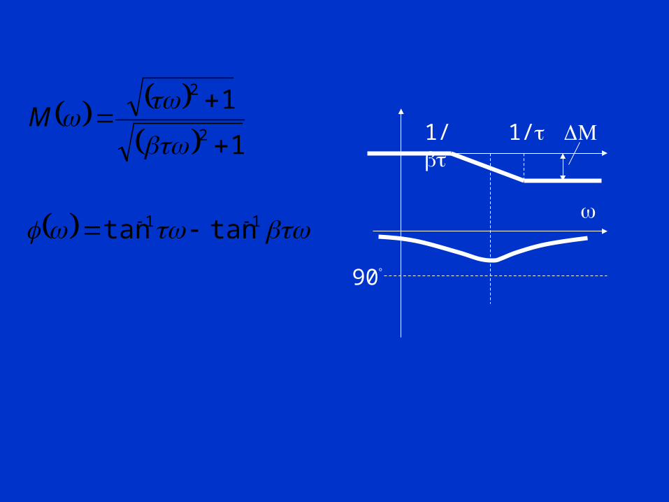
tantan
1
1
M
1/ 1/
90
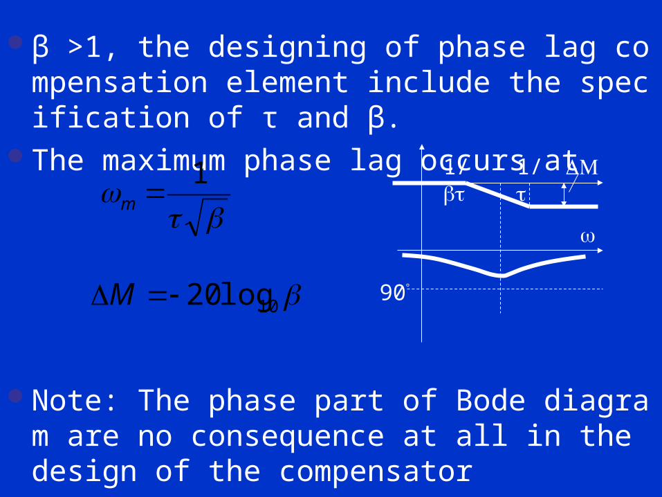
β >1, the designing of phase lag compensation element include the specification of τ and β.
The maximum phase lag occurs at
Note: The phase part of Bode diagram are no consequence at all in the design of the compensator
The attenuation at high frequency
1
m
10log20M
1/
1/
90
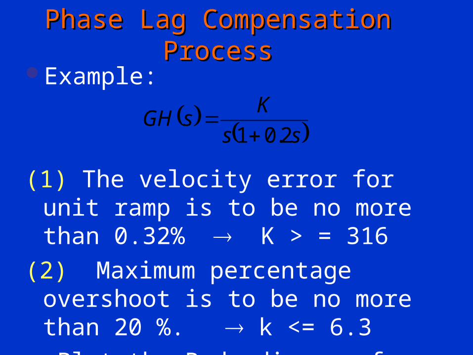
Example:
(1) The velocity error for unit ramp is to be no more than 0.32% K > = 316
(2) Maximum percentage overshoot is to be no more than 20 %. k <= 6.3
Plot the Bode diagram for K=316
Phase Lag Compensation ProcessPhase Lag Compensation Process
ss
KsGH
2.01
5 /rad s
45PM
60
40
20
0
0
-90
-180
dbM
( / )rad s1 10 100
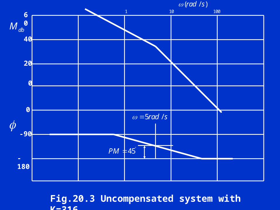
Fig.20.3 Uncompensated system with K=316.
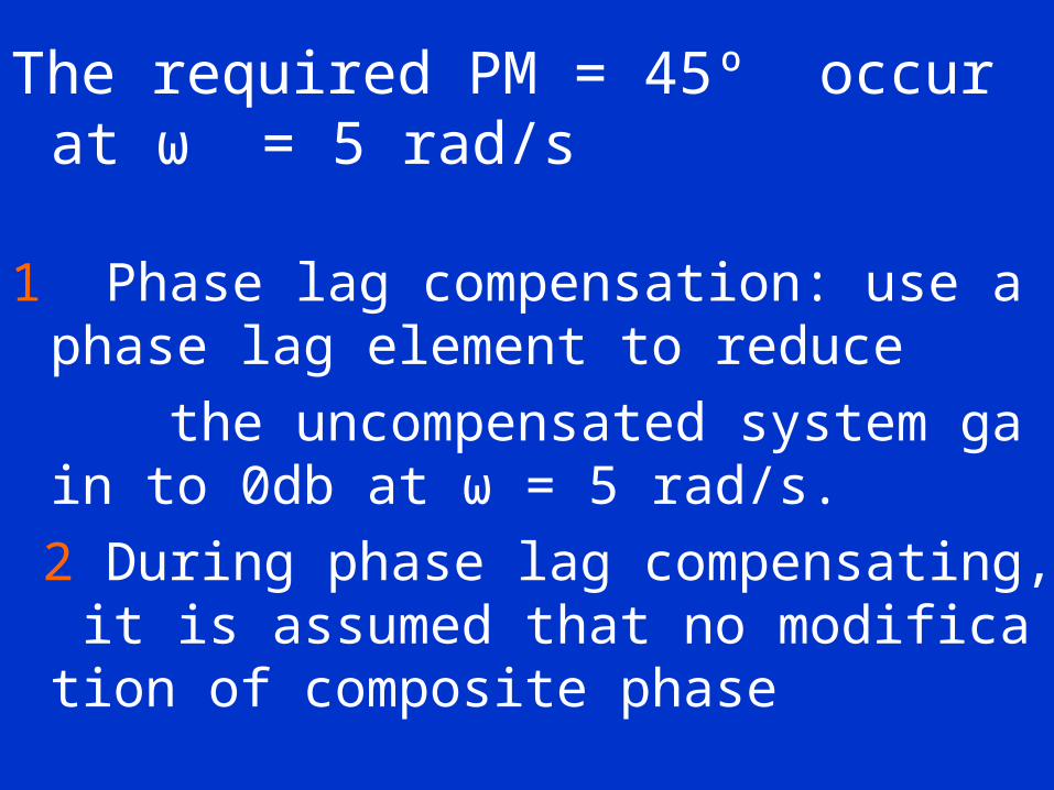
The required PM = 45º occur at ω = 5 rad/s
1 Phase lag compensation: use a phase lag element to reduce
the uncompensated system gain to 0db at ω = 5 rad/s.
2 During phase lag compensating, it is assumed that no modification of composite phase

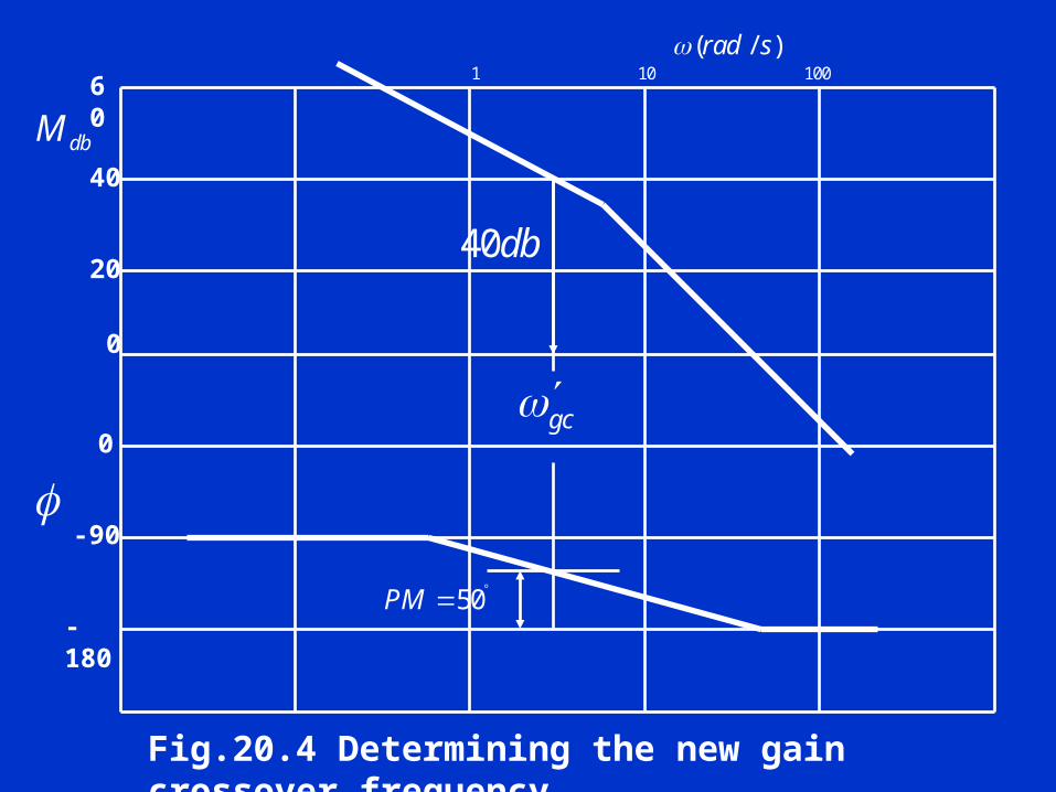
45º + 10% = 50º ω = 3 rad/s 3 New gain crossover frequency ωgc’=3 rad/s 4 At ωgc’= 3 rad/s, the magnitude must reduced from 40db to 0db
100 40log20 10
occurs. But a safety margin 10% is added to phase margin.
60
40
20
0
0
-90
-180
dbM
( / )rad s1 10 100
Fig.20.4 Determining the new gain crossover frequency.
50PM
gc
40db

Determine τ : the two break frequencies are at a lower frequency than ωgc’=3. This is determine by:
(1) The higher break frequency 1/ τ should at a frequency that the residual phase is no more than 10% for gain crossover frequency. Usually 1/ τ = ωgc’/10.
(2) The lower break frequency should not be too small to keep the bandwidth. Usually 1/ τ = ωgc’/10.

The compensator transfer function
The compensated open loop transfer fucntion
s
ssGc 3341
34.31
sss
ssGH
33412.01
34.31316
334
34.3
sradgc / 3.01.01

0.01 0.1 1.0 1060
40
20
0
0
-90
-180
-270
dbM
Compensated
magnitude
Compensated phase
40db
gc
50PM
Zmp
Fig.20.5 Bode diagram of compensated system
( / )rad s

1.8
2
1.6
1.4
1.2
1.0
0.8
0.6
0.4
0.2
00.2 0.4 0.6 0.8 1 1.2 1.4 1.6 1.8 2
00 1 2 3 4 5 6 7 8 9 10
0.2
0.4
0.6
0.8
1.0
1.2
Time (s) (a)
Time (s) (b)
Fig.20.6 Closed-loop step response of compensated system
compensated
Uncompensated
Am
plitu
deA
mpl
itude
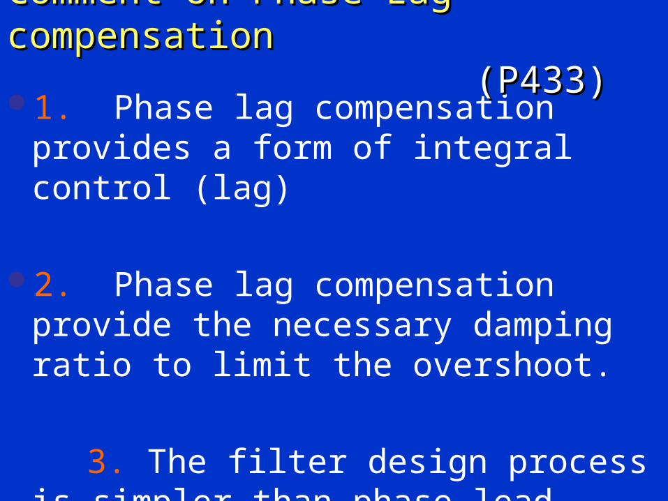
1. Phase lag compensation provides a form of integral control (lag)
2. Phase lag compensation provide the necessary damping ratio to limit the overshoot.
3. The filter design process is simpler than phase lead because the zero and pole break frequencies is not too critical.
Comment on Phase Lag compensationComment on Phase Lag compensation (P433)(P433)

4. The phase lag compensation reduces the open- ( close-) loop bandwidths.
5. The settling time is also increased considerably.
6. Phase lag compensation may change the phase margin by more than 90º (Phase lag < 90º Fig. 19.7)
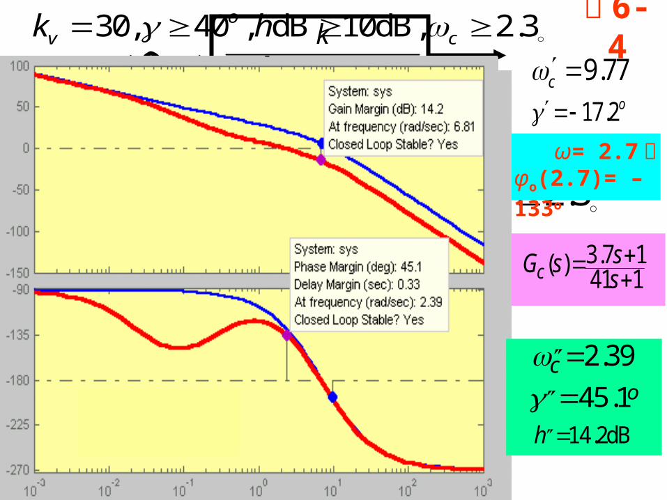
例 6-4
9.77c 17.2o
(0.1 )(0.2 1)
k
s s s
设计校正网络使图示系统30, 40 , dB 10dB, 2.3o
v ck h
30, 40 , dB 10dB, 2.3ov ck h
ω= 2.7 时φo(2.7)= –133o
3.7 1( )41 1csG ss
2.39c 45.1o
14.2dBh OK
Combined lead-lag compensation may allow more requirements to be met than by using either lead or lag compensation alone.
Lead- Lag CompensationLead- Lag Compensation

Lead-lag compensator may be constructed by connecting together a phase lead and a phase lag network in series. The value of α, β, τ, T are independent.
Transfer Function of Lead- Lag Transfer Function of Lead- Lag ElementElement
sTs
sTs
v
vsG
i
oc
11
11
1Riv ov2R
1C Buffer amplifier
2C3R
4R
Fig.20.7 Lead-lag from separate elements
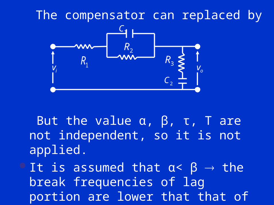
The compensator can replaced by
But the value α, β, τ, T are not independent, so it is not applied.
It is assumed that α< β the break frequencies of lag portion are lower that that of lead portion.
1Riv ov
2R
1C
2C
3R

1
1
1
T1
T
10log
10log
1020log
Fig.20.9 Bode diagram of lead-lag filter
dbM
0
0

The features of Bode diagram1. The filter provides attenuation only and no
gain
(α< β )
2. The low frequency gain is 1 while high
frequency gain is
10log20M

3. The phase angle first lag, then leads, but high- and low- frequency phases are both zeros.
4. The maximum phase lag and phase lead occur between their respective filter break frequencies.

Problem: Consider the system with open loop transfer function
Design a phase lag compensation element that enforces the following performance specificities on the closed loop system:
(1) A damping ratio of = 0.5
(2) A velocity error of no more than 10%
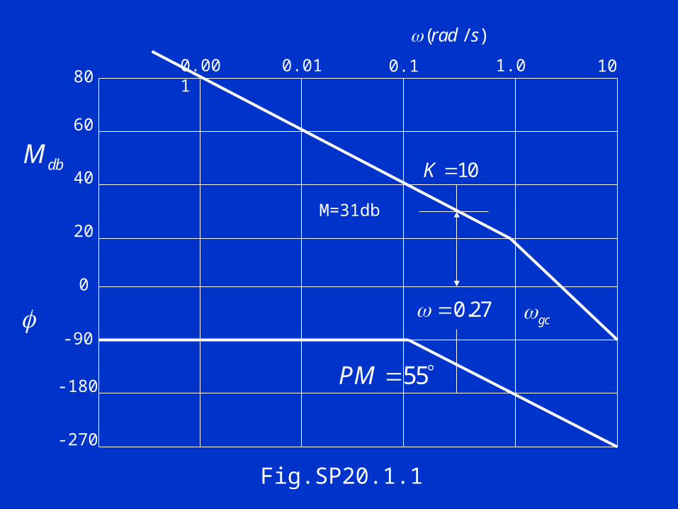
Sample Problem 20.1
21 ss
KsGH
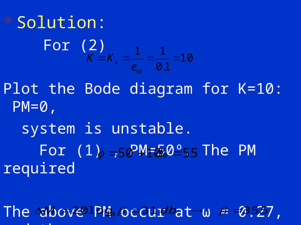
Solution: For (2)
Plot the Bode diagram for K=10: PM=0,
system is unstable.
For (1) , PM=50º. The PM required
The above PM occur at ω = 0.27, and the
corresponding magnitude is 31db.
101.0
11
ssv eKK
55%1050
5.35 31log20 10 dbM
dbM
0.001 0.01 0.1 1.0 10
-270
-180
-90
0
20
40
60
80
( / )rad s
10K
M=31db
55PM
0.27 gc
Fig.SP20.1.1

The high break frequency is set one decade below the new gain crossover frequency
ω = 0.27.
The compensated open loop transfer function
srad
srad
p
z
/ 00077.01
/ 027.01
s
s
s
ssGc 12961
371
1
1
sss
ssGHGc
129611
371102

0.001 0.01 0.1 1.0 10
( / )rad s
dbM
-270
-180
-90
0
20
40
60
80 A
compensated
compensated
E
gc
Fig.SP20.1.2
F
B
C D
HG

例 6-5 设未校正系统开环传递函数如下,试设计校正网络使: 1 )在最大指令速度为 180/s 时, 位置滞后误差不超过 1o; 2) 相角裕度为 45o±3o; 3) 幅值裕度不低于 10dB; 4) 动态过程调节时间 ts 不超过 3秒。
( )( / 6 1)( / 2 1)
kG s
s s s
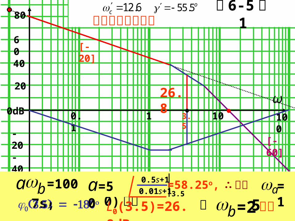
0dB
20
40
60
80
-20
-40
-60
-80
0.1 1 10 100
ω
[-20]
12.6c 55.5o
[-60]
取=45o,ts=2.7s, 由 (6-8) ~ (6-10) 求得
3.5
c
L0(3.5)=26.8dB
采用滞后超前校正
3.5
b取 =2 降阶ba =100, a=50
0.5s+1
0.01s+1=58.25o,
3.5∴ 可取
a =1
例 6-5图1
26.8
例 6-5图2
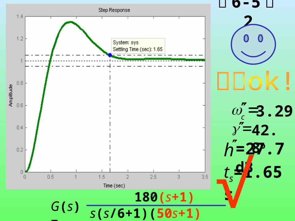
G(s) =180(s+1)
s(s/6+1)(50s+1)(0.01s+1)
3.29c 42.8o
h=27.7dB
ts=1.65s√
HomeworkHomework P461 20.4 P461 20.4