calc_01
6
Calculations 1. Problem 1. Determine the Norton and Th´ evenin equivalent of the voltage divider in Figure 1. using the voltage and current directions given. Figure 1. Voltage divider circuit Solution Let us determine the output voltage when the load is an open circuit by using the well-known equation of the voltage divider: U G = V CC · R 2 R 1 + R 2 =2.5V Next we shall calculate the output current when the load is a short circuit. If the output ports are shorted, so is resistor R 2 . Thus the supply voltage is connected to the ground through R 1 , the current of which can be determined using Ohm’s law: I G = V CC R 1 = 5 mA The value of the internal impedance is: R G = U G I G = 500 Ω The equivalent circuits can be seen in Figure 2. Figure 2. The Th´ evenin and Norton equivalents 1
description
sss
Transcript of calc_01
Calculations 1.
Problem 1.
Determine the Norton and Thevenin equivalent of the voltage divider in Figure 1. using the voltageand current directions given.
Figure 1. Voltage divider circuit
Solution
Let us determine the output voltage when the load is an open circuit by using the well-known equationof the voltage divider:
UG = VCC · R2
R1 + R2
= 2.5 V
Next we shall calculate the output current when the load is a short circuit. If the output ports areshorted, so is resistor R2. Thus the supply voltage is connected to the ground through R1, the currentof which can be determined using Ohm’s law:
IG =VCC
R1
= 5 mA
The value of the internal impedance is:
RG =UG
IG
= 500 Ω
The equivalent circuits can be seen in Figure 2.
Figure 2. The Thevenin and Norton equivalents
1

Problem 2.
Find appropriate values for the resistor R and the capacitor C in order to have a 100ms long logiclow value on the RESET input of the microcontroller when the supply voltage of 3.3V is switched on.The threshold voltage of the RESET input is 60% of the supply voltage. The threshold voltage is thevalue below which the logic circuit determines the input as a logic low and above it as a logic high.
Figure 3. Delay circuit on a reset input
Solution
The capacitor’s voltage as a function of time is:
VC(t) = VCC ·(1− e−
tR·C
)
Let us determine the time it takes for the voltage to rise to the 60% of the supply voltage:
0.6 · VCC = VCC ·(1− e−
tR·C
)
0.4 = e−t
R·C
Let us calculate the logarithm of both sides:
ln 0.4 = − t
R · CUsing the following logarithmic identity: a · log(b) = log (ba)
t = R · C · ln(2.5)
By using the approximation: e ≈ 2.5R · C = 100 ms
A possible solution for the problem is: R = 47 kΩ, C = 2.2 µF.
2
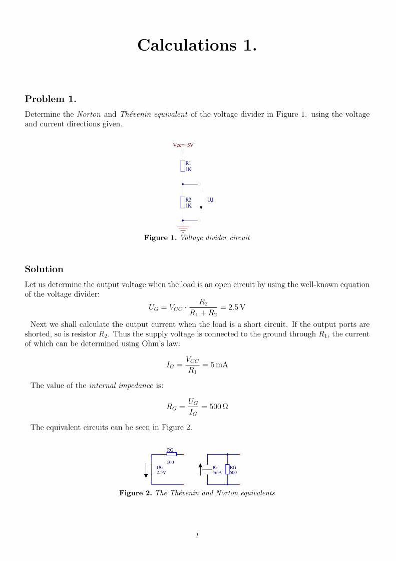
Problem 3.
Determine the current of the diode in Figure 4. using
(a) the VD = 0.7 V approximation.
(b) the more accurate model that was shown in class.
The model parameters of the 1N914 diode are the following: I0 = 2.52 nA, RS = 0.568 Ω, m = 1.752.Determine the error caused by the approximation.
Figure 4. Simple diode circuit
Solution
Using the VD = 0.7 V approximation, the current of the diode is
ID =VCC − VD
R= 4.3 mA
For a more accurate calculation, let us use a more precise diode characteristics:
VD = m · VT · ln(
I
IS
+ 1
)+ I ·RS
Using Kirchhof’s voltage law (KVL):
VCC = I ·R + VD = m · VT · ln(
I
IS
+ 1
)+ I · (R + RS)
This equation has to be solved. By solving it with Excel we get the following results: I = 4.34 mA,VD = 0.656 V. We were able to determine the current with a precision of 1% and the voltage with 7%.
3

Problem 4.
Determine the transfer characteristics of the circuits in Figure 5. All the resistors have a resistance of1 kΩ and the VD = 0.7 V approximation can be used for the diodes.
Figure 5. Diode circuits
Solution
The point where the diode starts to conduct has to be found in each case:
(a) If the input voltage is less than 0.7V the diode is closed and the output voltage is equal to theinput. If the input voltage is above 0.7V then the diode conducts and the output voltage equalsto the diode’s voltage (0.7V). The rest of the input voltage is dropped on the resistor.
(b) If the input voltage is less than 0.7V the diode is closed and the output voltage is 0V (as theresistor pulls the output voltage down to the ground). When the input voltage rises above 0.7Vthe diode starts to conduct and the output voltage is: Vout = Vin − 0.7
(c) If the input voltage is less than 0.7V the diode is closed and the output voltage equals to theinput voltage. If the input votage is above 0.7 V the diode is open and Vin − 0.7 V is dropped onthe two resistors of equal resistance. The output voltage equals to the sum of the voltage on thelower resistor and the diode:
Vout =(Vin − 0.7)
2+ 0.7
(d) If the input voltage is lower than 0.7V than the diode is closed and the output voltage is 0 V. Ifthe input voltage is higher than that then the diode conducts and Vin − 0.7 V voltage is droppedon the two resistors thus:
Vout =(Vin − 0.7)
2
Figure 6. The transfer characteristics of the circuits in Figure 5.
4

Problem 5.
In Figure 7. a voltage reference generator circuit using a Zener diode can be seen. The breakdownvoltage of the diode is 10V, its differential resistance is 10 Ω. The resistor R has a resistance of 1 kΩand the unstable supply voltage is 15V. The output is not loaded.
(a) Determine the output voltage.
(b) Calculate the output voltage’s ripple if that of the input voltage is 1 V.
(c) Calculate the Power Supply Rejection Ratio (PSRR) in dB.
Figure 7. Reference voltage generator circuit
Solution
(a) Let us use the equivalent circuit of the Zener diode for the breakdown range. The current based
Figure 8. Reference voltage generator with the equivalent circuit of the Zener diode
on Figure 8:
I =Vin − Vbr
R + rd
The output voltage is equal to the voltage dropped on the Zener diode:
Vout = Vbr + rd · I = Vbr +rd
R + rd
· (Vin − Vbr) =R
R + rd
· Vbr +rd
R + rd
· Vin = 10.05 V
By deriving the equation above and applying the approximation: rd ¿ R
∂Vout
∂Vin
=rd
R + rd
≈ rd
R
thus∆Vout ≈ rd
R·∆Vin = 10 mV
(b) The PSRR is the reciprocal of the above value:
PSSR = 20 · lgR
rd
≈ 40 dB
5
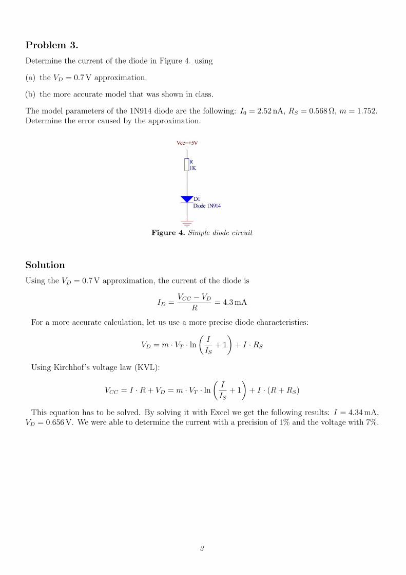
Problem 6.
Using the VD = 0.7 V approximation determine the transfer characteristics of the circuit below.
Figure 9. A full-wave rectifier
Solution
The diodes D1–D4 form a full-wave rectifier. For positive input voltages, the D1 and D2 diodes areopen and the D3 and D4 are closed. For negative input voltages it’s the other way around.
Current can only flow through the resistor R if the absolute value of the input voltage is bigger thanthe threshold voltage of two diodes. The structure of the diodes is such that whatever the sign of theinput voltage, the current of the resistor will always flow in the same direction thus the voltage dropon the resistor will always have the same sign. This is how the rectifying is accomplished.
Hence the transfer characteristics is the following:
Vout (Vin) =
0 if |Vin| < 2 · VD ≈ 1.4 V|Vin| − 2 · VD if |Vin| ≥ 2 · VD
Figure 10. The transfer characteristics of the full-wave rectifier
The output current will be the following:
Iout (Vin) =
0 if |Vin| < 2 · VD ≈ 1.4 V|Vin|−2·VD
Rif |Vin| ≥ 2 · VD
6