AD7303BR
16
R EV . 0 Information furnished by Analog Devices is believed to be accurate and reliable. However, no responsibility is assumed by Analog Devices for its use, nor for any infringements of patents or other rights of third parties which may result from its use. No license is granted by implication or otherwise under any patent or patent rights of Analog Devices. a +2.7 V to +5.5 V, Serial Input, Dual Voltage Output 8-Bit DAC AD7303 FUNCTIONAL BLOCK DIAGRAM I DAC A POWER ON RESET DIN SYNC SCLK REF VDD AD7303 VOUT A VOUT B GND I/V INPUT REGISTER MUX DAC REGISTER I/V INPUT REGISTER DAC REGISTER ÷2 16-BIT SHIFT REGISTER DATA (8) CONTROL (8) I DAC B FEATURES Two 8-Bit DACs in One Package 8-Pin DIP/SOIC and microSOIC Packages +2.7 V to +5.5 V Operation Internal & External Reference Capability Individual DAC Power-Down Function Three-Wire Serial Interface QSPI™, SPI™ and Microwire™ Compatible On-Chip Output Buffer Rail-to-Rail Operation On-Chip Control Register Low Power Oper ation: 2.3 mA @ 3.3 V Full Power-Down to 1 A max, typically 80 nA APPLICATIONS Portable Battery Powered Instruments Digital Gain and Offset Adjustment Programmable Voltage and Current Sources Programmable Attenuators PRODUCT HIGHLIGHTS 1. Low power , single supply oper ation . This part operates from a single +2.7 V to +5.5 V supply and consumes typically 15 mW at 5.5 V, making it ideal for battery powered applications. 2. The on-ch ip output bu ffer amplif iers allo w the outputs of the DACs to swing rail to rail with a settling time of typically 1.2 µ s. 3. Intern al or externa l referenc e capabil ity. 4. High speed serial interface with clock rates up to 30 MHz. 5. Indiv idual powe r-down of each DAC provided . When com- pletely powered down, the DAC consumes ty pically 80 nA. GENERAL DESCRIPTION The AD7303 is a dual, 8-bit voltage out DAC that operates from a single +2. 7 V to +5.5 V supply. Its on-chip precision out- put buffers allow the DAC outputs to swing rail to rail. This de- vice uses a versatile 3-wire serial interface that operates at clock rates up to 30 MHz, and is compatible with QSP I, SPI, microwire and digital signal processor interface standards. The serial input register is sixteen bits wide; 8 bits act as data bits for the DACs, and the remaining eight bits make up a control register. The on-chip control register is used to address the relevant DAC, to power down the complete device or an individual DAC, to select internal or external reference and to provide a synchronous loading facility for simultaneous update of the DAC outputs with a software LDAC function. The low power consumption of this part makes it ideally suited to portable battery operated equipment. The power consump- tion is 7.5 mW max at 3 V, reduc ing to les s than 3 µW in full power-down mode. The AD7303 is available in an 8-pin plastic dual in-line pack- age, 8-lead SOIC and microSOIC packages. QSPI and SPI are trademarks of Motorola. Microwire is a trademark of National Semiconductor. One Technology Way, P.O. Box 9106, Norwood, MA 02062-9106, U.S.A. Te l: 617 / 32 9 -47 0 0 Wor ld Wide Web Site: ht tp :// www.a na l og. co m Fax: 617/326-8703 © Analog Devices, Inc., 1997
-
Upload
zsori-corina -
Category
Documents
-
view
235 -
download
0
Transcript of AD7303BR
8/13/2019 AD7303BR
http://slidepdf.com/reader/full/ad7303br 1/16
8/13/2019 AD7303BR
http://slidepdf.com/reader/full/ad7303br 2/16
REV. 0–2–
AD7303–SPECIFICATIONS(VDD = +2.7 V to +5.5 V, Internal Reference; R L = 10 k to VDD and GND; CL = 100 pF
to GND; all specifications TMIN to TMAX unless otherwise noted)
Parameter B Versions1 Units Conditions/Comments
STATIC PERFORMANCEResolution 8 BitsRelative Accuracy ±1 LSB max Note 2Differential Nonlinearity ±1 LSB max Guaranteed MonotonicZero-Code Error @ +25°C 3 LSB max All Zeros Loaded to DAC RegisterFull-Scale Error –0.5 LSB typ All Ones Loaded to DAC Register
Gain Error3 +1 % FSR typZero-Code Temperature Coefficient 100 µV/°C typ
DAC REFERENCE INPUTREFIN Input Range 1 to VDD/2 V min to maxREFIN Input Impedance 10 ΜΩ typInternal Voltage Reference Error 4 ±1 % max
OUTPUT CHARACTERISTICSOutput Voltage Range 0 to VDD V min to maxOutput Voltage Settling Time 2 µs max Typically 1.2 µsSlew Rate 7.5 V/µs typDigital to Analog Glitch Impulse 0.5 nV-s typ 1 LSB Change Around Major CarryDigital Feedthrough 0.2 nV-s typDigital Crosstalk 0.2 nV-s typ
Analog Crosstalk ±0.2 LSB typDC Output Impedance 40 Ω typShort Circuit Current 14 mA typPower Supply Rejection Ratio 0.0001 %/% max ∆ VDD = ±10%
LOGIC INPUTSInput Current ±10 µA maxVINL , Input Low Voltage 0.8 V max VDD = +5 V
0.6 V max VDD = +3 VVINH, Input High Voltage 2.4 V min VDD = +5 V
2.1 V min VDD = +3 VPin Capacitance 5 pF max
POWER REQUIREMENTSVDD 2.7/5.5 V min/maxIDD (Normal Mode) Both DACs Active and Excluding Load Currents,
VDD = 3.3 V VIH = VDD, VIL = GND@ +25°C 2.1 mA max See Figure 8TMIN – TMAX 2.3 mA max
VDD = 5.5 V@ +25°C 2.7 mA maxTMIN – TMAX 3.5 mA max
IDD (Full Power-Down)@ +25°C 80 nA typ VIH = VDD, VIL = GNDTMIN – TMAX 1 µA max See Figure 19
NOTES1Temperature ranges are as follows: B Version, –40°C to +105°C.2Relative Accuracy is calculated using a reduced digital code range of 15 to 245.3Gain Error is specified between Codes 15 and 245. The actual error at Code 15 is typically 3 LSB.4Internal Voltage Reference Error = (Actual VREF – Ideal VREF/Ideal VREF) • 100. Ideal VREF = VDD/2, actual VREF = voltage on reference pin when internal reference
is selected.
Specifications subject to change without notice.
ORDERING GUIDE
Temperature Package
Model Range Options*
AD7303BN –40°C to +105°C N-8AD7303BR –40°C to +105°C SO-8AD7303BRM –40°C to +105°C RM-8
*N = Plastic DIP; R = SOIC; RM = microSOIC.
8/13/2019 AD7303BR
http://slidepdf.com/reader/full/ad7303br 3/16
AD7303
–3–REV. 0
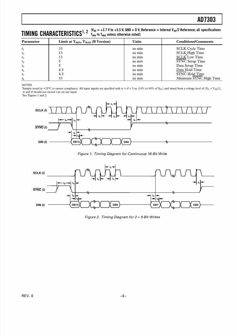
TIMING CHARACTERISTICS1, 2
Parameter Limit at TMIN, TMAX (B Version) Units Conditions/Comments
t1 33 ns min SCLK Cycle Timet2 13 ns min SCLK High Time
t3 13 ns min SCLK
Low Timet4 5 ns min SYNC Setup Timet5 5 ns min Data Setup Timet6 4.5 ns min Data Hold Timet7 4.5 ns min SYNC Hold Timet8 33 ns min Minimum SYNC High Time
NOTES1Sample tested at +25°C to ensure compliance. All input signals are specified with tr = tf = 5 ns (10% to 90% of VDD) and timed from a voltage level of (VIL + VIH)/2,tr and tf should not exceed 1 µs on any input.
2See Figures 1 and 2.
SCLK (I)
SYNC (I)
DIN (I) DB15 DB0
t5t6
t2 t3
t4t7 t4t8
t1
Figure 1. Timing Diagram for Continuous 16-Bit Write
SCLK (I)
SYNC (I)
DIN (I) DB15 DB8
t5
t6
t2 t3
t4t7
DB7 DB0
t5
t6
t8
t1
Figure 2. Timing Diagram for 2 × 8-Bit Writes
(VDD = +2.7 V to +5.5 V; GND = 0 V; Reference = Internal V DD /2 Reference; all specifications
TMIN to TMAX unless otherwise noted)
8/13/2019 AD7303BR
http://slidepdf.com/reader/full/ad7303br 4/16
AD7303
–4– REV. 0
ABSOLUTE MAXIMUM RATINGS*
(TA = +25°C unless otherwise noted)
VDD to GND . . . . . . . . . . . . . . . . . . . . . . . . . . –0.3 V to +7 V
Reference Input Voltage to GND . . . . –0.3 V to VDD + 0.3 VDigital Input Voltage to GND . . . . . . . –0.3 V to VDD + 0.3 VVOUT A, VOUT B to GND . . . . . . . . . . . –0.3 V to VDD + 0.3 VOperating Temperature Range
Commercial (B Version) . . . . . . . . . . . . . –40°C to +105°CStorage Temperature Range . . . . . . . . . . . . –65°C to +150°C Junction Temperature . . . . . . . . . . . . . . . . . . . . . . . . . +150°CPlastic DIP Package, Power Dissipation . . . . . . . . . . 800 mWθ JA Thermal Impedance . . . . . . . . . . . . . . . . . . . . . 117°C/WLead Temperature (Soldering, 10 sec) . . . . . . . . . . . +260°C
WARNING!
ESD SENSITIVE DEVICE
CAUTION
ESD (electrostatic discharge) sensitive device. Electrostatic charges as high as 4000 V readily
accumulate on the human body and test equipment and can discharge without detection.
Although the AD7303 features proprietary ESD protection circuitry, permanent damage may
occur on devices subjected to high energy electrostatic discharges. Therefore, proper ESDprecautions are recommended to avoid performance degradation or loss of functionality.
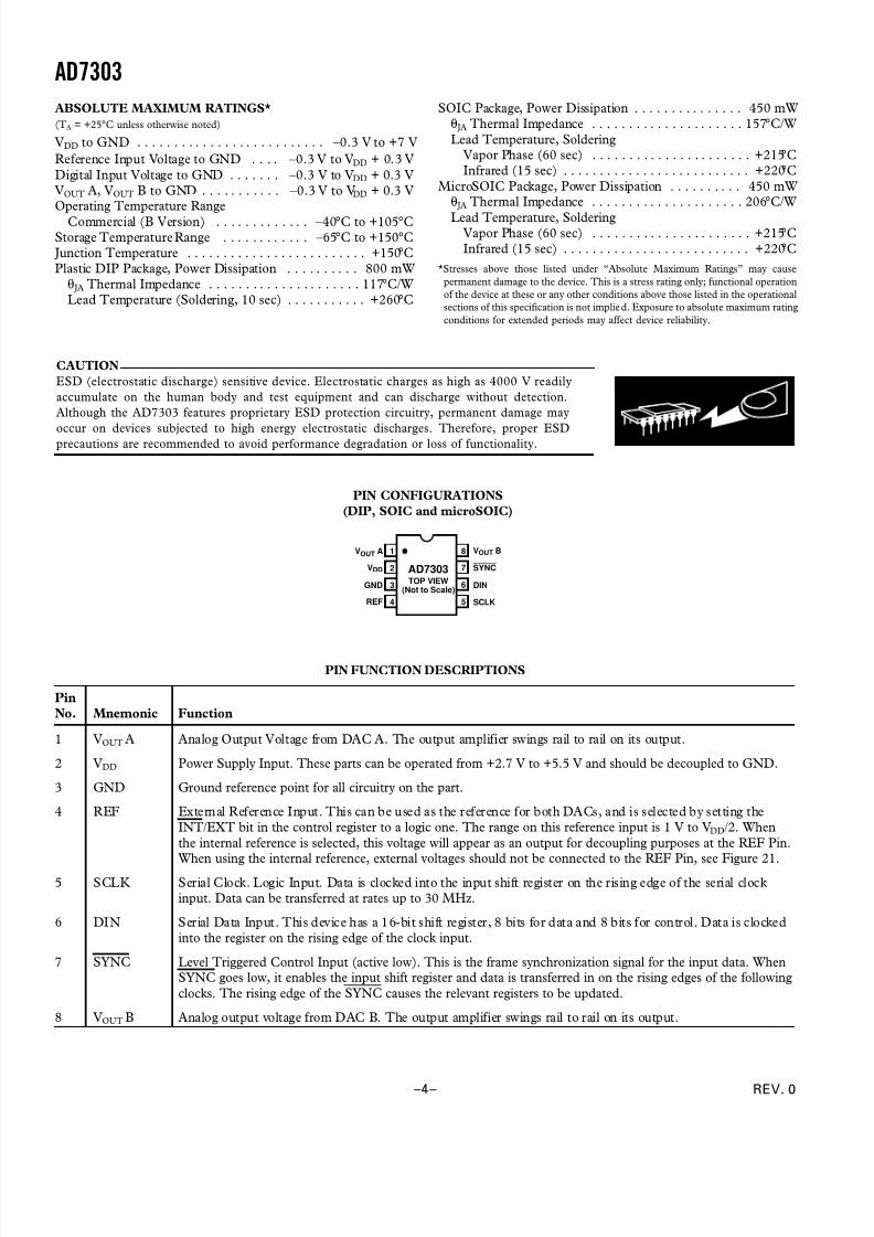
PIN CONFIGURATIONS
(DIP, SOIC and microSOIC)
1
2
3
4
8
7
6
5
TOP VIEW(Not to Scale)
AD7303
VOUT A
SCLK
DIN
SYNC
VOUT B
VDD
GND
REF
PIN FUNCTION DESCRIPTIONS
Pin
No. Mnemonic Function
1 VOUT A Analog Output Voltage from DAC A. The output amplifier swings rail to rail on its output.
2 VDD Power Supply Input. These parts can be operated from +2.7 V to +5.5 V and should be decoupled to GND.
3 GND Ground reference point for all circuitry on the part.
4 REF External Reference Input. This can be used as the reference for both DACs, and is selected by setting theINT/EXT bit in the control register to a logic one. The range on this reference input is 1 V to VDD/2. Whenthe internal reference is selected, this voltage will appear as an output for decoupling purposes at the REF Pin.When using the internal reference, external voltages should not be connected to the REF Pin, see Figure 21.
5 SCLK Serial Clock. Logic Input. Data is clocked into the input shift register on the rising edge of the serial clockinput. Data can be transferred at rates up to 30 MHz.
6 DIN Serial Data Input. This device has a 16-bit shift register, 8 bits for data and 8 bits for control. Data is clockedinto the register on the rising edge of the clock input.
7 SYNC Level Triggered Control Input (active low). This is the frame synchronization signal for the input data. WhenSYNC goes low, it enables the input shift register and data is transferred in on the rising edges of the followingclocks. The rising edge of the SYNC causes the relevant registers to be updated.
8 VOUT B Analog output voltage from DAC B. The output amplifier swings rail to rail on its output.
SOIC Package, Power Dissipation . . . . . . . . . . . . . . . 450 mWθ JA Thermal Impedance . . . . . . . . . . . . . . . . . . . . . 157°C/WLead Temperature, Soldering
Vapor Phase (60 sec) . . . . . . . . . . . . . . . . . . . . . . +215°CInfrared (15 sec) . . . . . . . . . . . . . . . . . . . . . . . . . . +220°C
MicroSOIC Package, Power Dissipation . . . . . . . . . . 450 mWθ JA Thermal Impedance . . . . . . . . . . . . . . . . . . . . . 206°C/W
Lead Temperature, SolderingVapor Phase (60 sec) . . . . . . . . . . . . . . . . . . . . . . +215°CInfrared (15 sec) . . . . . . . . . . . . . . . . . . . . . . . . . . +220°C
*Stresses above those listed under “Absolute Maximum Ratings” may cause
permanent damage to the device. This is a stress rating only; functional operationof the device at these or any other conditions above those listed in the operationalsections of this specification is not implied. Exposure to absolute maximum rating
conditions for extended periods may affect device reliability.
8/13/2019 AD7303BR
http://slidepdf.com/reader/full/ad7303br 5/16
AD7303
–5–REV. 0
TERMINOLOGYINTEGRAL NONLINEARITY
For the DACs, relative accuracy or endpoint nonlinearity is ameasure of the maximum deviation, in LSBs, from a straightline passing through the endpoints of the DAC transfer func-tion. A graphical representation of the transfer curve is shownin Figure 15.
DIFFERENTIAL NONLINEARITY
Differential nonlinearity is the difference between the measuredchange and the ideal 1 LSB change of any two adjacent codes. Aspecified differential nonlinearity of ±1 LSB maximum ensuresmonotonicity.
ZERO CODE ERROR
Zero code error is the measured output voltage from VOUT of either DAC when zero code (all zeros) is loaded to the DAClatch. It is due to a combination of the offset errors in the DACand output amplifier. Zero-scale error is expressed in LSBs.
GAIN ERROR
This is a measure of the span error of the DAC. It is the devia-tion in slope of the DAC transfer characteristic from idealexpressed as a percent of the full-scale value. Gain error is calcu-lated between Codes 15 and 245.
FULL-SCALE ERROR
Full-Scale Error is a measure of the output error when the DAClatch is loaded with FF Hex. Full-scale error includes the offseterror.
DIGITAL-TO-ANALOG GLITCH IMPULSE
Digital-to-analog glitch impulse is the impulse injected into theanalog output when the digital inputs change state with theDAC selected and the software LDAC used to update the DACIt is normally specified as the area of the glitch in nV-s and ismeasured when the digital input code is changed by 1 LSB atthe major carry transition.
DIGITAL FEEDTHROUGH
Digital feedthrough is a measure of the impulse injected into theanalog output of a DAC from the digital inputs of the sameDAC, but is measured when the DAC is not updated. It isspecified in nV-s and measured with a full-scale code change onthe data bus, i.e., from all 0s to all 1s and vice versa.
DIGITAL CROSSTALK
Digital crosstalk is the glitch impulse transferred to the outputof one converter due to a digital code change to another DAC.It is specified in nV-s.
ANALOG CROSSTALK
Analog crosstalk is a change in output of any DAC in responseto a change in the output of the other DAC. It is measured inLSBs.
POWER SUPPLY REJECTION RATIO (PSRR)
This specification indicates how the output of the DAC isaffected by changes in the power supply voltage. Power supplyrejection ratio is quoted in terms of % change in output per %of change in VDD for full-scale output of the DAC. VDD is varied± 10%. This specification applies to an external reference onlybecause the output voltage will track the VDD voltage when in-ternal reference is selected.
8/13/2019 AD7303BR
http://slidepdf.com/reader/full/ad7303br 6/16
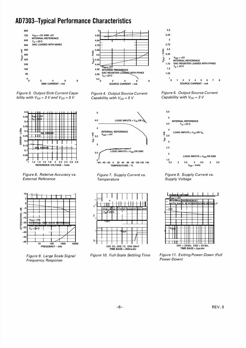
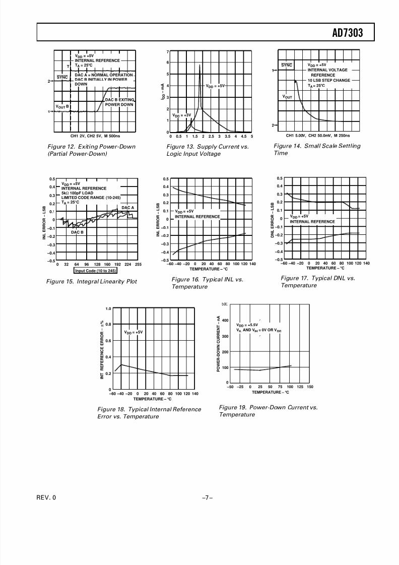
AD7303–Typical Performance Characteristics
–6– REV. 0
VDD = +5V AND +3V
INTERNAL REFERENCE
TA = 25C
DAC LOADED WITH 00HEX
SINK CURRENT – mA
V O U T – m
V
800
00 82 4 6
720
400
249
160
80
640
560
320
480
Figure 3. Output Sink Current Capa-
bility with V DD = 3 V and V DD = 5 V
REFERENCE VOLTAGE – Volts
E R R O R –
L S B s
0.5
01 1.2 2.81.4 1.6 1.8 2.2 2.4 2.62
0.45
0.25
0.15
0.1
0.05
0.4
0.35
0.2
0.3
VDD = +5V
TA = 25C
INL ERROR
DNL ERROR
Figure 6. Relative Accuracy vs.
External Reference
FREQUENCY – kHz
A T T E N U A T I O N –
d B
1 10 10000100 1000
10
5
–40
0
–5
–10
–15
–20
–25
–30
–35
VDD = +5V
TA = 25°C
EXTERNAL SINE WAVE REFERENCE
DAC REGISTER LOADED WITH FFHEX
Figure 9. Large Scale Signal
Frequency Response
SOURCE CURRENT – mA
V O U
T –
V o
l t s
0 2 84 6
5
4.92
4.2
4.84
4.76
4.68
4.6
4.524.44
4.36
4.28
VDD = +5V
TA = 25°C
INTERNAL REFERENCE
DAC REGISTER LOADED WITH FFHEX
Figure 4. Output Source Current
Capability with V DD = 5 V
–60 –40 –20 0 20 40 60 80 100 120 140
TEMPERATURE – C
5
3.5
2
I D D – m A
4.5
4
3
2.5 LOGIC INPUTS = VDD OR GND
INTERNAL REFERENCE VDD = +5V
LOGIC INPUTS = VIH
OR VIL
Figure 7. Supply Current vs.
Temperature
TSYNC
VOUT
VDD = +3V
INTERNAL VOLTAGE REFERENCEFULL SCALE CODE CHANGE 00H-FFHTA = 25°C
1
3
2
VOUT
CH1 5V, CH2 1V, CH3 20mVTIME BASE = 200ns/div
Figure 10. Full-Scale Settling Time
SOURCE CURRENT – mA
3.5
10 1 82 3 4 5 6 7
3.25
2.5
2.25
1.75
1.25
3
2.75
2
1.5
V O U T –
V o
l t s
VDD = +3V
TA = 25°C
INTERNAL REFERENCE DAC REGISTER LOADED WITH FFHEX
Figure 5. Output Source Current
Capability with V DD = 3 V
VDD – Volts
I D D – m A
5.5
1.5
5
3.5
3
2.5
2
4.5
4
2.5 3 5.53.5 4 4.5 5
LOGIC INPUTS = VDD OR GND
LOGIC INPUTS = VIH OR VIL
TA = 25°C INTERNAL REFERENCE
Figure 8. Supply Current vs.
Supply Voltage
SYNC
VOUT
POWER UP TIME VDD = +5V
INTERNAL REFERENCEBOTH DACS IN POWER DOWN INITIALLY
1
2
CH1 = 2V/div, CH2 = 5V/div,TIME BASE = 2µs/div
Figure 11. Exiting Power-Down (Full
Power-Down)
8/13/2019 AD7303BR
http://slidepdf.com/reader/full/ad7303br 7/16
AD7303
–7–REV. 0
T
←DAC A = NORMAL OPERATION DAC B INITIALLY IN POWER DOWN
1
2
VOUT B
SYNC
DAC B EXITINGPOWER DOWN
CH1 2V, CH2 5V, M 500ns
VDD = +5V
INTERNAL REFERENCE TA = 25C
Figure 12. Exiting Power-Down
(Partial Power-Down)
Input Code (10 to 245)
I N L E R R O R – L S B
0 25532 64 96 128 160 192 224
DAC B
DAC A
VDD = +5V
INTERNAL REFERENCE 5kΩ 100pF LOAD
LIMITED CODE RANGE (10-245) TA = 25°C
–0.5
0.4
0.1
–0.1
–0.3
–0.4
0.3
0.2
0
–0.2
0.5
Figure 15. Integral Linearity Plot
I D D
– m A
0 50.5 1 1.5 2 2.5 3 3.5 4 4.5
4
0
7
6
2
1
5
3
VDD = +5V
VDD = +3V
Figure 13. Supply Current vs.
Logic Input Voltage
VDD = +5V
INTERNAL REFERENCE
0.5
0.4
0.3
0.2
0.1
0
–0.1
–0.2
–0.3
–0.4
–0.5 –60 –40 –20 0 20 40 60 80 100 120 140
I N L E R R O R – L S B
TEMPERATURE – C
Figure 16. Typical INL vs.
Temperature
2
1
VOUT
CH1 5.00V, CH2 50.0mV, M 250ns
SYNC VDD = +5V
INTERNAL VOLTAGE
REFERENCE
10 LSB STEP CHANGE
TA = 25C
Figure 14. Small Scale Settling
Time
VDD = +5V
INTERNAL REFERENCE
0.5
0.4
0.3
0.2
0.1
0
–0.1
–0.2
–0.3
–0.4
–0.5 –60 –40 –20 0 20 40 60 80 100 120 140
TEMPERATURE – C
D N L E R R O R – L S B
Figure 17. Typical DNL vs.
Temperature
TEMPERATURE – C
400
200
100
0
300
–50 0 50 100 150
VDD = +5.5V
VIL AND VIH = 0V OR VDD
P O W E R - D O W N C U R R E N T – n A
–25 25 75 125
Figure 19. Power-Down Current vs.
Temperature
VDD = +5V
0.6
0.4
0.2
0 –60 –40 –20 0 20 40 60 80 100 120 140
TEMPERATURE – C
I N T
R E F E R E N C E E R R O R – %0.8
1.0
Figure 18. Typical Internal Reference
Error vs. Temperature
8/13/2019 AD7303BR
http://slidepdf.com/reader/full/ad7303br 8/16
AD7303
–8– REV. 0
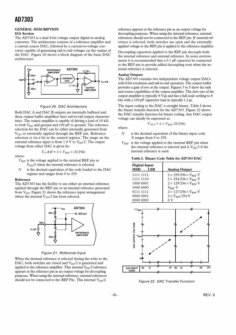
GENERAL DESCRIPTION
D/A Section
The AD7303 is a dual 8-bit voltage output digital-to-analogconverter. The architecture consists of a reference amplifier anda current source DAC, followed by a current-to-voltage con-verter capable of generating rail-to-rail voltages on the output of the DAC. Figure 20 shows a block diagram of the basic DAC
architecture.
REFERENCEAMPLIFIER
OUTPUTAMPLIFIER
VO A/B
VDD
REF
AD7303
CURRENTDAC
11.7kΩ
30kΩ
11.7kΩ
30kΩ
Figure 20. DAC Architecture
Both DAC A and DAC B outputs are internally buffered and
these output buffer amplifiers have rail-to-rail output character-istics. The output amplifier is capable of driving a load of 10 kΩto both VDD and ground and 100 pF to ground. The referenceselection for the DAC can be either internally generated fromVDD or externally applied through the REF pin. Referenceselection is via a bit in the control register. The range on theexternal reference input is from 1.0 V to VDD/2. The outputvoltage from either DAC is given by:
V O A/B = 2 × V REF × ( N /256)where:
V REF is the voltage applied to the external REF pin orVDD/2 when the internal reference is selected.
N is the decimal equivalent of the code loaded to the DACregister and ranges from 0 to 255.
Reference
The AD7303 has the facility to use either an external referenceapplied through the REF pin or an internal reference generatedfrom VDD. Figure 21 shows the reference input arrangementwhere the internal VDD/2 has been selected.
30kΩ
30kΩ
REFERENCE
AMPLIFIER
AD7303
REF
0.1µF
VDD
INT/EXT
Figure 21. Reference Input
When the internal reference is selected during the write to theDAC, both switches are closed and VDD/2 is generated andapplied to the reference amplifier. This internal VDD/2 referenceappears at the reference pin as an output voltage for decouplingpurposes. When using the internal reference, external referencesshould not be connected to the REF Pin. This internal VDD/2
reference appears at the reference pin as an output voltage fordecoupling purposes. When using the internal reference, externalreferences should not be connected to the REF pin. If external ref-erence is selected, both switches are open and the externallyapplied voltage to the REF pin is applied to the reference amplifier.
Decoupling capacitors applied to the REF pin decouple boththe internal reference and external reference. In noisy environ-ments it is recommended that a 0.1 µF capacitor be connectedto the REF pin to provide added decoupling even when the in-ternal reference is selected.
Analog Outputs
The AD7303 contains two independent voltage output DACswith 8-bit resolution and rail-to-rail operation. The output bufferprovides a gain of two at the output. Figures 3 to 5 show the sinkand source capabilities of the output amplifier. The slew rate of theoutput amplifier is typically 8 V/µs and has a full-scale settling to 8bits with a 100 pF capacitive load in typically 1.2 µs.
The input coding to the DAC is straight binary. Table I showsthe binary transfer function for the AD7303. Figure 22 showsthe DAC transfer function for binary coding. Any DAC output
voltage can ideally be expressed as:
V OUT = 2 × V REF ( N /256)
where:
N is the decimal equivalent of the binary input code. N ranges from 0 to 255.
V REF is the voltage applied to the external REF pin whenthe external reference is selected and is VDD/2 if theinternal reference is used.
Table I. Binary Code Table for AD7303 DAC
Digital Input
MSB . . . LSB Analog Output
1111 1111 2 × 255/256 × VREF V1111 1110 2 × 254/256 × VREF V1000 0001 2 × 129/256 × VREF V1000 0000 VREF V0111 1111 2 × 127/256 × VREF V0000 0001 2 × VREF/256 V0000 0000 0 V
2.VREF
VREF
0
D A C O U T P U T
V O L T A G E
00 01DAC INPUTCODE
FF80 81 FE7F
Figure 22. DAC Transfer Function
8/13/2019 AD7303BR
http://slidepdf.com/reader/full/ad7303br 9/16
AD7303
–9–REV. 0
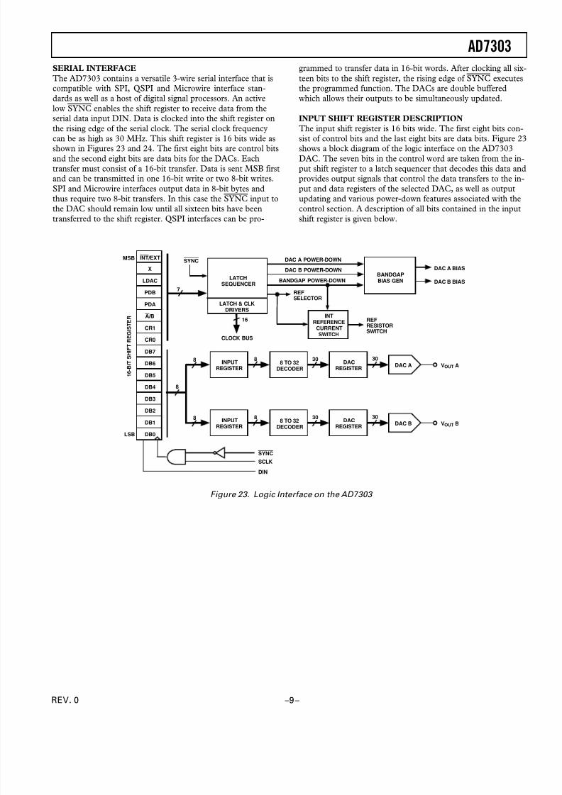
grammed to transfer data in 16-bit words. After clocking all six-teen bits to the shift register, the rising edge of SYNC executesthe programmed function. The DACs are double bufferedwhich allows their outputs to be simultaneously updated.
INPUT SHIFT REGISTER DESCRIPTION
The input shift register is 16 bits wide. The first eight bits con-
sist of control bits and the last eight bits are data bits. Figure 23shows a block diagram of the logic interface on the AD7303DAC. The seven bits in the control word are taken from the in-put shift register to a latch sequencer that decodes this data andprovides output signals that control the data transfers to the in-put and data registers of the selected DAC, as well as outputupdating and various power-down features associated with thecontrol section. A description of all bits contained in the inputshift register is given below.
SERIAL INTERFACE
The AD7303 contains a versatile 3-wire serial interface that iscompatible with SPI, QSPI and Microwire interface stan-dards as well as a host of digital signal processors. An activelow SYNC enables the shift register to receive data from theserial data input DIN. Data is clocked into the shift register onthe rising edge of the serial clock. The serial clock frequency
can be as high as 30 MHz. This shift register is 16 bits wide asshown in Figures 23 and 24. The first eight bits are control bitsand the second eight bits are data bits for the DACs. Eachtransfer must consist of a 16-bit transfer. Data is sent MSB firstand can be transmitted in one 16-bit write or two 8-bit writes.SPI and Microwire interfaces output data in 8-bit bytes andthus require two 8-bit transfers. In this case the SYNC input tothe DAC should remain low until all sixteen bits have beentransferred to the shift register. QSPI interfaces can be pro-
DB0
DB1
DB2
DB3
DB4
DB5
DB6
DB7
INT/ EXT
CR0
CR1
A/ B
PDA
PDB
LDAC
X
8
8
LATCHSEQUENCER
7
MSB
LSB
DAC A POWER-DOWN
DAC B POWER-DOWN
BANDGAP POWER-DOWN
LATCH & CLKDRIVERS
16
REFSELECTOR
INTREFERENCE
CURRENTSWITCH
CLOCK BUS
REFRESISTORSWITCH
DAC A BIAS
DAC B BIAS
1 6 - B
I T S H I F T R E G I S T E R
DIN
SYNC
DACREGISTER
30
DAC A VOUT A30
8 TO 32DECODER
INPUTREGISTER
8
SYNC
SCLK
BANDGAPBIAS GEN
8 DACREGISTER
30DAC B VOUT B
308 TO 32DECODER
INPUTREGISTER
8
Figure 23. Logic Interface on the AD7303
8/13/2019 AD7303BR
http://slidepdf.com/reader/full/ad7303br 10/16
AD7303
–10– REV. 0
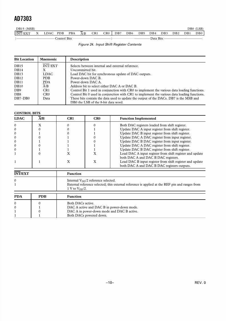
Bit Location Mnemonic Description
DB15 INT/EXT Selects between internal and external reference.DB14 X Uncommitted bit.DB13 LDAC Load DAC bit for synchronous update of DAC outputs.DB12 PDB Power-down DAC B.DB11 PDA Power-down DAC A.DB10 A/B Address bit to select either DAC A or DAC B.DB9 CR1 Control Bit 1 used in conjunction with CR0 to implement the various data loading functions.DB8 CR0 Control Bit 0 used in conjunction with CR1 to implement the various data loading functions.DB7–DB0 Data These bits contain the data used to update the output of the DACs. DB7 is the MSB and
DB0 the LSB of the 8-bit data word.
CONTROL BITS
LDAC A/B CR1 CR0 Function Implemented
0 X 0 0 Both DAC registers loaded from shift register.0 0 0 1 Update DAC A input register from shift register.0 1 0 1 Update DAC B input register from shift register.0 0 1 0 Update DAC A DAC register from input register.0 1 1 0 Update DAC B DAC register from input register.0 0 1 1 Update DAC A DAC register from shift register.0 1 1 1 Update DAC B DAC register from shift register.1 0 X X Load DAC A input register from shift register and update
both DAC A and DAC B DAC registers.1 1 X X Load DAC B input register from shift register and update
both DAC A and DAC B DAC registers outputs.
INT/EXT Function
0 Internal VDD/2 reference selected.1 External reference selected; this external reference is applied at the REF pin and ranges from
1 V to VDD/2.
PDA PDB Function
0 0 Both DACs active.0 1 DAC A active and DAC B in power-down mode.1 0 DAC A in power-down mode and DAC B active.1 1 Both DACs powered down.
DB15 (MSB) DB0 (LSB)
INT /EXT X LDAC PDB PBA A/B CR1 CR0 DB7 DB6 DB5 DB4 DB3 DB2 DB1 DB0
|––––––––––––––––––––––––– Control Bits –––––––––––––––––––––––––|––––––––––––––––––––––––– Data Bits –––––––––––––––––––––––––|
Figure 24. Input Shift Register Contents
8/13/2019 AD7303BR
http://slidepdf.com/reader/full/ad7303br 11/16
AD7303
–11–REV. 0
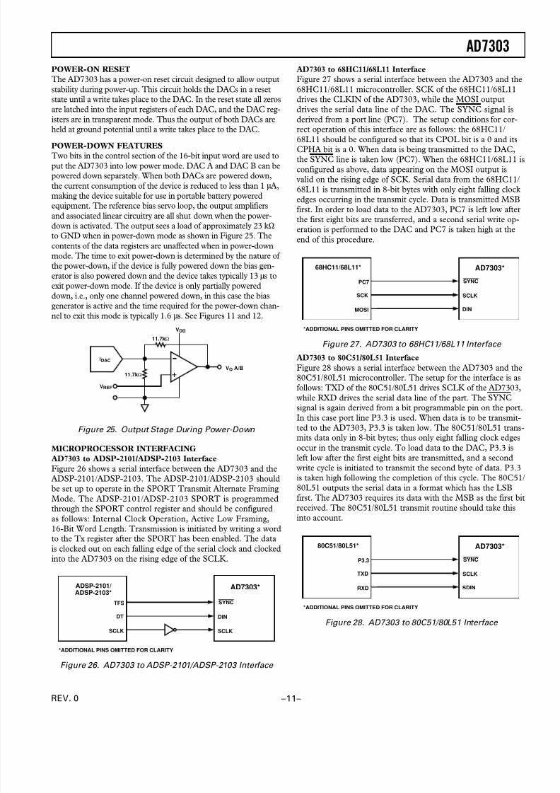
POWER-ON RESET
The AD7303 has a power-on reset circuit designed to allow outputstability during power-up. This circuit holds the DACs in a resetstate until a write takes place to the DAC. In the reset state all zerosare latched into the input registers of each DAC, and the DAC reg-isters are in transparent mode. Thus the output of both DACs areheld at ground potential until a write takes place to the DAC.
POWER-DOWN FEATURES
Two bits in the control section of the 16-bit input word are used toput the AD7303 into low power mode. DAC A and DAC B can bepowered down separately. When both DACs are powered down,the current consumption of the device is reduced to less than 1 µA,making the device suitable for use in portable battery poweredequipment. The reference bias servo loop, the output amplifiersand associated linear circuitry are all shut down when the power-down is activated. The output sees a load of approximately 23 kΩto GND when in power-down mode as shown in Figure 25. Thecontents of the data registers are unaffected when in power-downmode. The time to exit power-down is determined by the nature of the power-down, if the device is fully powered down the bias gen-
erator is also powered down and the device takes typically 13 µs toexit power-down mode. If the device is only partially powereddown, i.e., only one channel powered down, in this case the biasgenerator is active and the time required for the power-down chan-nel to exit this mode is typically 1.6 µs. See Figures 11 and 12.
VO A/B
VDD
11.7kΩ
11.7kΩ
VREF
IDAC
Figure 25. Output Stage During Power-Down
MICROPROCESSOR INTERFACING
AD7303 to ADSP-2101/ADSP-2103 Interface
Figure 26 shows a serial interface between the AD7303 and theADSP-2101/ADSP-2103. The ADSP-2101/ADSP-2103 shouldbe set up to operate in the SPORT Transmit Alternate FramingMode. The ADSP-2101/ADSP-2103 SPORT is programmedthrough the SPORT control register and should be configuredas follows: Internal Clock Operation, Active Low Framing,16-Bit Word Length. Transmission is initiated by writing a wordto the Tx register after the SPORT has been enabled. The datais clocked out on each falling edge of the serial clock and clocked
into the AD7303 on the rising edge of the SCLK.
SCLK
ADSP-2101/ADSP-2103*
DT
*ADDITIONAL PINS OMITTED FOR CLARITY
SYNC
DIN
SCLK
AD7303*
TFS
Figure 26. AD7303 to ADSP-2101/ADSP-2103 Interface
AD7303 to 68HC11/68L11 Interface
Figure 27 shows a serial interface between the AD7303 and the68HC11/68L11 microcontroller. SCK of the 68HC11/68L11drives the CLKIN of the AD7303, while the MOSI outputdrives the serial data line of the DAC. The SYNC signal isderived from a port line (PC7). The setup conditions for cor-rect operation of this interface are as follows: the 68HC11/
68L11 should be configured so that its CPOL bit is a 0 and itsCPHA bit is a 0. When data is being transmitted to the DAC,the SYNC line is taken low (PC7). When the 68HC11/68L11 isconfigured as above, data appearing on the MOSI output isvalid on the rising edge of SCK. Serial data from the 68HC11/68L11 is transmitted in 8-bit bytes with only eight falling clockedges occurring in the transmit cycle. Data is transmitted MSBfirst. In order to load data to the AD7303, PC7 is left low afterthe first eight bits are transferred, and a second serial write op-eration is performed to the DAC and PC7 is taken high at theend of this procedure.
SCLK
68HC11/68L11*
SCK
*ADDITIONAL PINS OMITTED FOR CLARITY
SYNC
DINMOSI
AD7303*
PC7
Figure 27. AD7303 to 68HC11/68L11 Interface
AD7303 to 80C51/80L51 Interface
Figure 28 shows a serial interface between the AD7303 and the80C51/80L51 microcontroller. The setup for the interface is asfollows: TXD of the 80C51/80L51 drives SCLK of the AD7303,while RXD drives the serial data line of the part. The SYNCsignal is again derived from a bit programmable pin on the port.
In this case port line P3.3 is used. When data is to be transmit-ted to the AD7303, P3.3 is taken low. The 80C51/80L51 trans-mits data only in 8-bit bytes; thus only eight falling clock edgesoccur in the transmit cycle. To load data to the DAC, P3.3 isleft low after the first eight bits are transmitted, and a secondwrite cycle is initiated to transmit the second byte of data. P3.3is taken high following the completion of this cycle. The 80C51/80L51 outputs the serial data in a format which has the LSBfirst. The AD7303 requires its data with the MSB as the first bitreceived. The 80C51/80L51 transmit routine should take thisinto account.
SCLK
80C51/80L51*
TXD
*ADDITIONAL PINS OMITTED FOR CLARITY
SYNC
SDINRXD
AD7303*
P3.3
Figure 28. AD7303 to 80C51/80L51 Interface
8/13/2019 AD7303BR
http://slidepdf.com/reader/full/ad7303br 12/16
AD7303
–12– REV. 0
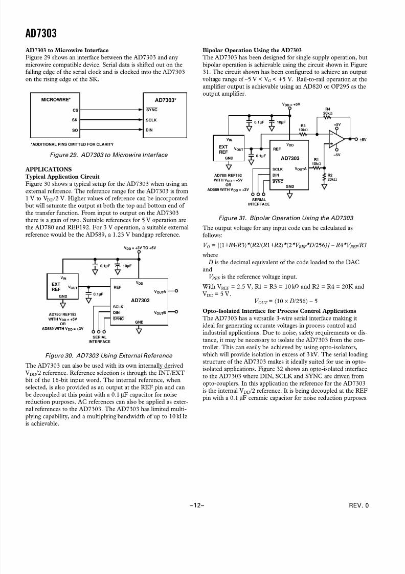
AD7303 to Microwire Interface
Figure 29 shows an interface between the AD7303 and anymicrowire compatible device. Serial data is shifted out on thefalling edge of the serial clock and is clocked into the AD7303on the rising edge of the SK.
SCLK
MICROWIRE*
SK
*ADDITIONAL PINS OMITTED FOR CLARITY
SYNC
DINSO
AD7303*
CS
Figure 29. AD7303 to Microwire Interface
APPLICATIONS
Typical Application Circuit
Figure 30 shows a typical setup for the AD7303 when using anexternal reference. The reference range for the AD7303 is from
1 V to VDD/2 V. Higher values of reference can be incorporatedbut will saturate the output at both the top and bottom end of the transfer function. From input to output on the AD7303there is a gain of two. Suitable references for 5 V operation arethe AD780 and REF192. For 3 V operation, a suitable externalreference would be the AD589, a 1.23 V bandgap reference.
AD7303
VOUTA
VOUTB
10µF0.1µF
VDD = +3V TO +5V
VDD
GND
AD780/ REF192
WITH VDD = +5V
OR
AD589 WITH VDD = +3V
REF
SCLK
DIN
SYNC
GND
VOUT
VIN
0.1µF
SERIALINTERFACE
EXTREF
Figure 30. AD7303 Using External Reference
The AD7303 can also be used with its own internally derivedVDD/2 reference. Reference selection is through the INT/EXTbit of the 16-bit input word. The internal reference, whenselected, is also provided as an output at the REF pin and canbe decoupled at this point with a 0.1 µF capacitor for noise
reduction purposes. AC references can also be applied as exter-nal references to the AD7303. The AD7303 has limited multi-plying capability, and a multiplying bandwidth of up to 10 kHzis achievable.
Bipolar Operation Using the AD7303
The AD7303 has been designed for single supply operation, butbipolar operation is achievable using the circuit shown in Figure31. The circuit shown has been configured to achieve an outputvoltage range of –5 V < VO < +5 V. Rail-to-rail operation at theamplifier output is achievable using an AD820 or OP295 as theoutput amplifier.
R110kΩ
R420kΩ
R310kΩ
+5V
–5V
±5V
AD7303
VOUTA
10µF0.1µF
VDD = +5V
VDD
GND
AD780/ REF192
WITH VDD = +5V
OR
AD589 WITH VDD = +3V
REF
SCLK
DIN
SYNC
GND
VOUT
VIN
0.1µF
SERIALINTERFACE
EXTREF
R220kΩ
Figure 31. Bipolar Operation Using the AD7303
The output voltage for any input code can be calculated asfollows:
V O = [(1+R4/R3)* (R2/ (R1+R2)* (2*V REF *D/ 256 )] – R4*V REF /R3
whereD is the decimal equivalent of the code loaded to the DAC
andV REF is the reference voltage input.
With VREF = 2.5 V, R1 = R3 = 10 kΩ and R2 = R4 = 20K andVDD = 5 V.
V OUT = (10 × D/256) – 5Opto-Isolated Interface for Process Control Applications
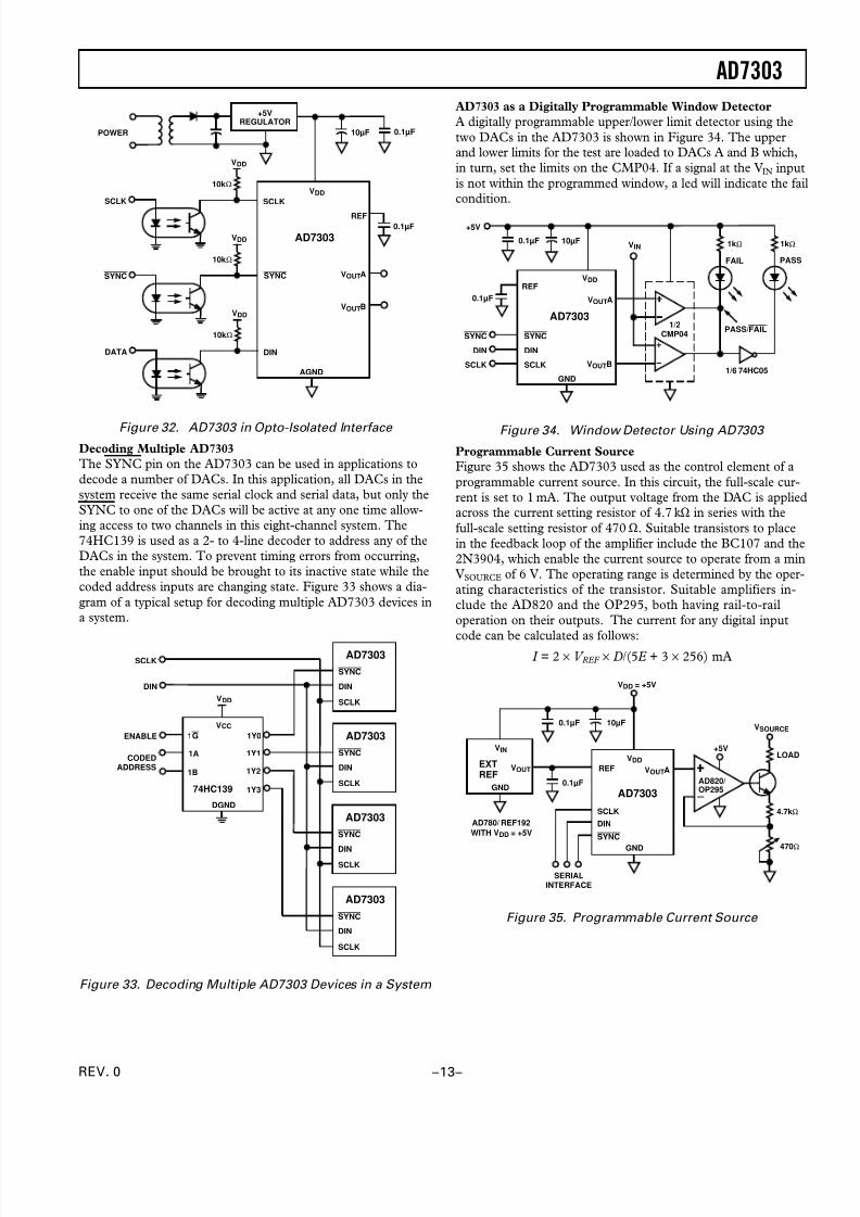
The AD7303 has a versatile 3-wire serial interface making itideal for generating accurate voltages in process control andindustrial applications. Due to noise, safety requirements or dis-tance, it may be necessary to isolate the AD7303 from the con-troller. This can easily be achieved by using opto-isolators,which will provide isolation in excess of 3kV. The serial loadingstructure of the AD7303 makes it ideally suited for use in opto-isolated applications. Figure 32 shows an opto-isolated interfaceto the AD7303 where DIN, SCLK and SYNC are driven fromopto-couplers. In this application the reference for the AD7303is the internal VDD/2 reference. It is being decoupled at the REFpin with a 0.1 µF ceramic capacitor for noise reduction purposes.
8/13/2019 AD7303BR
http://slidepdf.com/reader/full/ad7303br 13/16
8/13/2019 AD7303BR
http://slidepdf.com/reader/full/ad7303br 14/16
AD7303
–14– REV. 0
AD7303 to 68HC11 Interface Program Source Code
*
PORTC EQU $1003 Port C Control Register
* "SYNC, 0, 0, 0, 0, 0, 0, 0"
DDRC EQU $1007 Port C Data Direction
PORTD EQU $1008 Port D Data Register
* "0, 0, 0, SCLK, DIN, 0, 0, 0"
DDRD EQU $1009 Port D Data Direction
SPCR EQU $1028 SPI Control Register
* "SPIE, SPE, DWOM, MSTR, CPOL, CPHA, SPR1, SPR0"
SPSR EQU $1029 SPI Status Register
* "SPIF, WCOL, 0, MODF, 0, 0, 0, 0"
SPDR EQU $102A SPI Data Register, Read Buffer, Write Shifter*
* SDI RAM Variables: DIN 1 is eight MSBs, Control BYTE
DIN 2 is eight LSBs, Data BYTE
DAC requires 2*8-bit Writes
DIN1 EQU $00 DIN BYTE 1: " INT/EXT, X, LDAC, PDB, PBA, A/B, CR1, CR0"
DIN2 EQU $01 DIN BYTE 2: " DB7, DB6, DB5, DB4, DB3, DB2, DB1, DB0"
*
ORG $C000 Start of users ram
INIT LDS #$CFFF Top of C page Ram
*LDAA #$80 1, 0, 0, 0, 0, 0, 0, 0
* SYNC is High
STAA PORTC Initialize Port C Outputs
LDAA #$80 1, 0, 0, 0, 0, 0, 0, 0
STAA DDRC SYNC enabled as output
*
LDAA #$00 0, 0, 0, 0, 0, 0, 0, 0
* SCLK is low, DIN is low
STAA PORTD Initialize Port D outputs
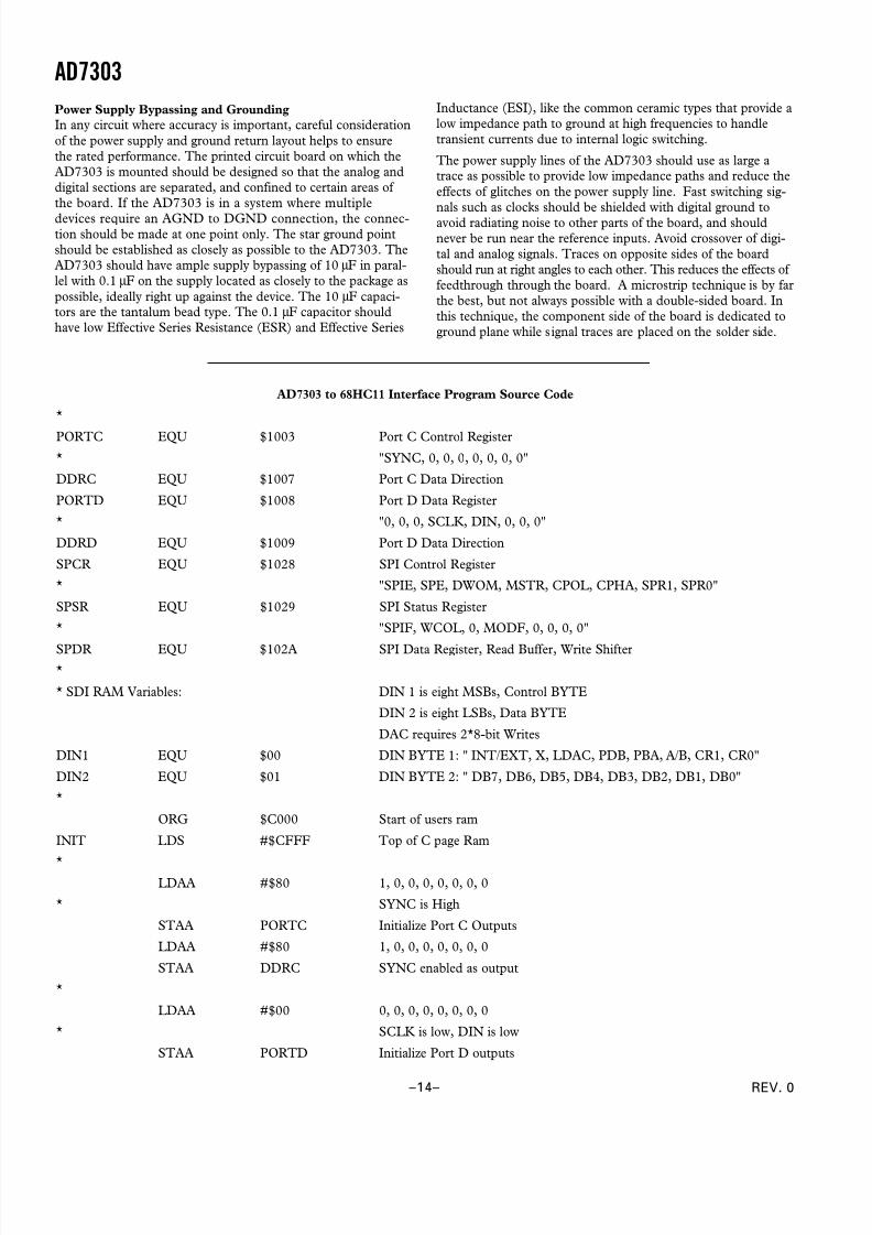
Power Supply Bypassing and Grounding
In any circuit where accuracy is important, careful considerationof the power supply and ground return layout helps to ensurethe rated performance. The printed circuit board on which theAD7303 is mounted should be designed so that the analog anddigital sections are separated, and confined to certain areas of the board. If the AD7303 is in a system where multiple
devices require an AGND to DGND connection, the connec-tion should be made at one point only. The star ground pointshould be established as closely as possible to the AD7303. TheAD7303 should have ample supply bypassing of 10 µF in paral-lel with 0.1 µF on the supply located as closely to the package aspossible, ideally right up against the device. The 10 µF capaci-tors are the tantalum bead type. The 0.1 µF capacitor shouldhave low Effective Series Resistance (ESR) and Effective Series
Inductance (ESI), like the common ceramic types that provide alow impedance path to ground at high frequencies to handletransient currents due to internal logic switching.
The power supply lines of the AD7303 should use as large atrace as possible to provide low impedance paths and reduce theeffects of glitches on the power supply line. Fast switching sig-nals such as clocks should be shielded with digital ground toavoid radiating noise to other parts of the board, and shouldnever be run near the reference inputs. Avoid crossover of digi-tal and analog signals. Traces on opposite sides of the boardshould run at right angles to each other. This reduces the effects of feedthrough through the board. A microstrip technique is by farthe best, but not always possible with a double-sided board. Inthis technique, the component side of the board is dedicated toground plane while signal traces are placed on the solder side.
8/13/2019 AD7303BR
http://slidepdf.com/reader/full/ad7303br 15/16
AD7303
–15–REV. 0
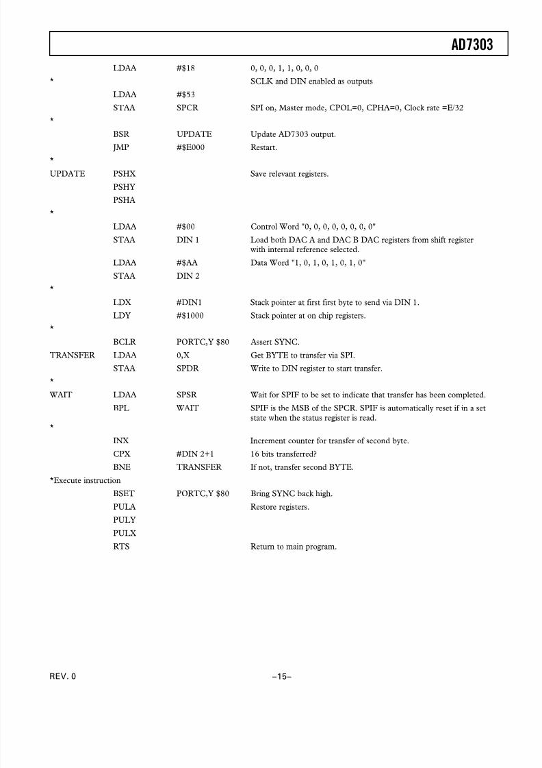
LDAA #$18 0, 0, 0, 1, 1, 0, 0, 0
* SCLK and DIN enabled as outputs
LDAA #$53
STAA SPCR SPI on, Master mode, CPOL=0, CPHA=0, Clock rate =E/32
*
BSR UPDATE Update AD7303 output. JMP #$E000 Restart.
*
UPDATE PSHX Save relevant registers.
PSHY
PSHA
*
LDAA #$00 Control Word "0, 0, 0, 0, 0, 0, 0, 0"
STAA DIN 1 Load both DAC A and DAC B DAC registers from shift registerwith internal reference selected.
LDAA #$AA Data Word "1, 0, 1, 0, 1, 0, 1, 0"
STAA DIN 2
*
LDX #DIN1 Stack pointer at first first byte to send via DIN 1.
LDY #$1000 Stack pointer at on chip registers.
*
BCLR PORTC,Y $80 Assert SYNC.
TRANSFER LDAA 0,X Get BYTE to transfer via SPI.
STAA SPDR Write to DIN register to start transfer.
*
WAIT LDAA SPSR Wait for SPIF to be set to indicate that transfer has been completed.
BPL WAIT SPIF is the MSB of the SPCR. SPIF is automatically reset if in a setstate when the status register is read.
*
INX Increment counter for transfer of second byte.
CPX #DIN 2+1 16 bits transferred?
BNE TRANSFER If not, transfer second BYTE.
*Execute instruction
BSET PORTC,Y $80 Bring SYNC back high.
PULA Restore registers.
PULY
PULX
RTS Return to main program.
8/13/2019 AD7303BR
http://slidepdf.com/reader/full/ad7303br 16/16
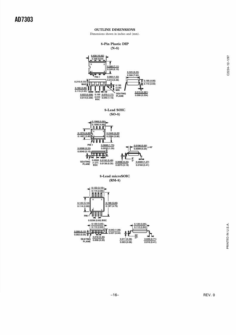
AD7303
OUTLINE DIMENSIONS
Dimensions shown in inches and (mm).
8-Pin Plastic DIP
(N-8)
8
1 4
5
0.430 (10.92)
0.348 (8.84)
0.280 (7.11)
0.240 (6.10)
PIN 1
SEATINGPLANE
0.022 (0.558)
0.014 (0.356)
0.060 (1.52)
0.015 (0.38)0.210 (5.33)
MAX 0.130(3.30)MIN
0.070 (1.77)
0.045 (1.15)
0.100(2.54)BSC
0.160 (4.06)
0.115 (2.93)
0.325 (8.25)
0.300 (7.62)
0.015 (0.381)
0.008 (0.204)
0.195 (4.95)
0.115 (2.93)
8-Lead SOIC
(SO-8)
0.1968 (5.00)
0.1890 (4.80)
8 5
41
0.2440 (6.20)
0.2284 (5.80)
PIN 1
0.1574 (4.00)
0.1497 (3.80)
0.0688 (1.75)
0.0532 (1.35)
SEATINGPLANE
0.0098 (0.25)
0.0040 (0.10)
0.0192 (0.49)
0.0138 (0.35)
0.0500(1.27)BSC
0.0098 (0.25)
0.0075 (0.19)
0.0500 (1.27)
0.0160 (0.41)
8°0°
0.0196 (0.50)
0.0099 (0.25)x 45°
8-Lead microSOIC(RM-8)
8 5
41
0.122 (3.10)
0.114 (2.90)
0.199 (5.05)
0.187 (4.75)
PIN 1
0.0256 (0.65) BSC
0.122 (3.10)
0.114 (2.90)
SEATINGPLANE
0.006 (0.15)
0.002 (0.05)0.018 (0.46)
0.008 (0.20)
0.043 (1.09)
0.037 (0.94)
0.120 (3.05)
0.112 (2.84)
0.011 (0.28)
0.003 (0.08)
0.028 (0.71)
0.016 (0.41)
33°27°
0.120 (3.05)
0.112 (2.84)