
VADA Lab.SungKyunKwan Univ. 1 Clock and Interconnect Issues 1998. 6 조 준 동.
44
SungKyunKwan Univ . 1 VADA Lab. Clock and Interconnect Issues 1998. 6 조 조 조
-
Upload
chad-patrick -
Category
Documents
-
view
217 -
download
3
Transcript of VADA Lab.SungKyunKwan Univ. 1 Clock and Interconnect Issues 1998. 6 조 준 동.
SungKyunKwan Univ.
1VADA Lab.
Clock and Interconnect Issues
1998. 6
조 준 동

SungKyunKwan Univ.
2VADA Lab.
Clock and power glossary• Clock buffer: circuit element to isolate and amplify incoming clock signal. • Clock tree: design technique to achieve balanced delays and loads in the clock buffers. • Gated clock: clock line that can control clock transmission to the operating circuits. • Ground bounce: the change in ground (vss) reference levels due to current in the ground
line. • Ground loop: the noise caused in the ground line(s) due to unbalanced IR drops in the gr
ound line. • Insertion delay: the time from clock pad to individual flop-flops. • IR drop: the voltage drop caused by the current I through the resistor R. • Jitter: the change in period to period timing in a clock signal. • Latency: the time for a clock to become available in the circuit. • Multiphase clock: clocking system with more than one phase may be overlapping or no
n-overlapping. Biphase-clock and complement, Quadrature-clocks separated by a phase angle of 90 degree
• PLL: Phase-Locked Loop, a variable frequency generator locked to a source signal. • Skew: the maximum difference in clock arrival time between any two flip-flops. • Slew rate: also called rise time or fall time. The time for a signal to go from one level to t
he other level.

SungKyunKwan Univ.
3VADA Lab.
Global Distribution: Clocks and Power• When ASICs are built on a deep submicron process with over 5 million gates and a clock frequency
greater than 250 MHz, the designer must consider many details in the clock and power circuitry. Normally these circuit elements are not given much thought; power is drawn from the rails drawn across the top and bottom of the page, and the clock has ideal characteristics: a square wave running at the specified frequency.
• In reality, many other effects need to be evaluated in the clocking and power distribution areas of the design when the total chip power consumption will be in the range of tens to over 100 W and the clock power can be as much as half of the total power consumption. The clocking scheme cannot be assumed to be a clean, uniform signal network. It might be a complicated distribution structure with architectures ranging from a large distributed clock buffer for the high-performance chips to a complex system with multiple derived sub-clocks to help manage power consumption. The interaction between clocks and power consumption may require the ability to generate clock signals which can be stopped in the inactive sections to minimize power consumption. The power and ground system will take up about half of the available package pins to be able to handle the tens of amperes of average current consumed by the IC.
• Many side effects of the basic IC process will have to be addressed to make the chip meet all the requirements of speed, power, and silicon area. If the supply voltage is reduced to take advantage of the power savings available at a lower supply voltage, noise margins and leakage currents may become significant problems. The various secondary effects within the system, like voltage drops on the supply lines, ground bounce, crosstalk, and glitches, may exacerbate the problems by adding enough noise to the system to decrease the clock slew rates and the clock rise and fall times.

SungKyunKwan Univ.
4VADA Lab.
Timing-Density-Clock-Power• This further exacerbates the power consumption problems by making the big clock buffers stay in the
high current linear portions of their transfer curves for greater amounts of each clock cycle. In addition, the clock network has many signals switching simultaneously, adding large power surges and a very large potential for crosstalk and interference to the clock and power distribution sub-systems.
• The most basic problems facing designers are managing the skew in the clock system (which entails getting the clock everywhere at the same time), supplying sufficient clock drive to operate all of the clocked elements in the system, and getting operating power to all active circuit elements. For single-frequency clock systems, the tradeoffs are speed, power consumption, and area. The problems with skew and the process of balancing the delays across the chip occur in parallel with the increases in density and complexity. Tom Katsioulas, marketing director of the IC design group of Cadence Design Systems (San Jose, CA), notes that the timing, density, clock, and power are intricately related in the following ways:
– Downsizing cells to reduce power may degrade timing. – Upsizing cells to improve timing degrades power and area. – Timing-driven placement may increase wire length and power. – Clock generation before placement yields high skew. – Clock creation without wire delays affects power and delay. – Clock creation after placement adds area and affect density. – Large load count yields high clock delay and affects timing. – Post placement ECOs may require clock redesign.
SungKyunKwan Univ.
5VADA Lab.
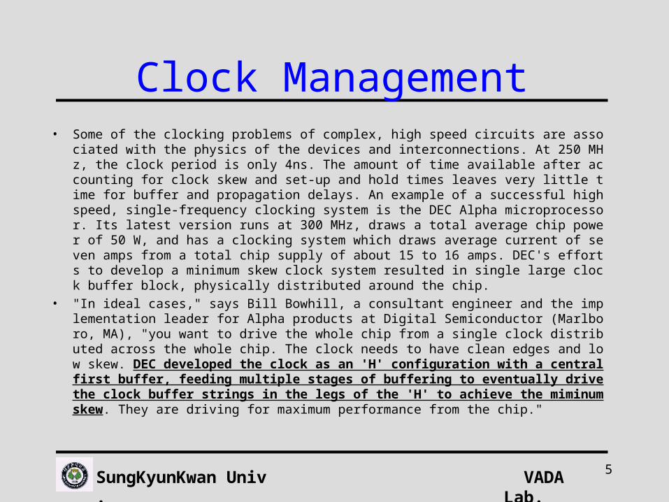
Clock Management• Some of the clocking problems of complex, high speed circuits are associated with the p
hysics of the devices and interconnections. At 250 MHz, the clock period is only 4ns. The amount of time available after accounting for clock skew and set-up and hold times leaves very little time for buffer and propagation delays. An example of a successful high speed, single-frequency clocking system is the DEC Alpha microprocessor. Its latest version runs at 300 MHz, draws a total average chip power of 50 W, and has a clocking system which draws average current of seven amps from a total chip supply of about 15 to 16 amps. DEC's efforts to develop a minimum skew clock system resulted in single large clock buffer block, physically distributed around the chip.
• "In ideal cases," says Bill Bowhill, a consultant engineer and the implementation leader for Alpha products at Digital Semiconductor (Marlboro, MA), "you want to drive the whole chip from a single clock distributed across the whole chip. The clock needs to have clean edges and low skew. DEC developed the clock as an 'H' configuration with a central first buffer, feeding multiple stages of buffering to eventually drive the clock buffer strings in the legs of the 'H' to achieve the miminum skew. They are driving for maximum performance from the chip."

SungKyunKwan Univ.
6VADA Lab.
Clock Management• The large clock buffers lead to high power consumption, often as large as 30 to 50 percent of the tota
l chip power consumption, as well as noise problems due to the large current spikes generated when the buffers switch. An alternative approach is to distribute the buffers into the clock tree. This reduces the power consumption by requiring buffers of smaller size and also helps the reliability aspects by reducing the size of the current spike.
• The clock system and the wide word datapaths all switching at the same time increase the possibility for glitches and higher peak switching currents. They put additional loads on the power delivery systems. The resulting datapath skews will require close scrutiny of the datapath localization and grouping, as well as careful analysis of pipeline lengths. The careful analysis of the signal paths relative to the clocks is critical to making a working integrated circuit.
• "In synthesized circuits," says Charlie Xiaoli Huang, a senior architect at Epic Design Technology (Santa Clara, CA), "the software tries to make all paths the same length. This makes all data paths complete at the same time, which generates glitches and power surges at the end of each clock cycle. This effect gets worse at higher speeds."
• To develop a working clock distribution topology, EDA and ASIC vendors have many tools for implementing a balanced clock tree. This technology seeks the physical location of the delay path's electrical middle. The nature of this optimization work has been mainly manual adjustment of the generated clock structure. The path delay associated with the clock lines and buffer stages needs to be adjusted so each buffer sees the same path lengths and loads. The number and strengths of the buffers can create a long first cycle latency delay.

SungKyunKwan Univ.
7VADA Lab.
Clock Power Consumption• Clocking schemes and power distribution are going to be affected by the system require
ments. The areas for compromise are power, area, and performance. If one of the areas is defined as much more critical than the others, it will drive the design. For example, if performance is the key parameter, a single point clock with sufficient buffers to drive all the circuitry would be the best choice. The tradeoff would be in a clock system which draws up to half of the total system current. An intermediate solution might be a multiply driven clock spine (see "Deep submicron design clocking techniques").
• If all of the circuitry did not need to run at same speed, derived multiple clocks could be generated from the master reference clock. The sections will get clocks appropriate for their functions. Why have a 250 MHz clock for a serial I/O channel controller? This could save some more power since the frequency term in the power equation has now been reduced for much of the on-chip circuitry.
• Obviously, if the designer gates the clock signals to unused sections of the chip, with the understanding that the gate delay will exacerbate the clock skew and clock edge uncertainty for those sections, this keeps the clocks from toggling the inputs of sections with no data changes. If the gate is used in place of a buffer in the clock tree section, the clock tree does not require an additional level of buffers to match the delays due to the extra gate levels.
SungKyunKwan Univ.
8VADA Lab.
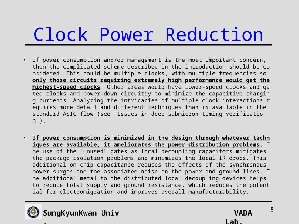
Clock Power Reduction• If power consumption and/or management is the most important concern, then the compl
icated scheme described in the introduction should be considered. This could be multiple clocks, with multiple frequencies so only those circuits requiring extremely high performance would get the highest-speed clocks. Other areas would have lower-speed clocks and gated clocks and power-down circuitry to minimize the capacitive charging currents. Analyzing the intricacies of multiple clock interactions requires more detail and different techniques than is available in the standard ASIC flow (see "Issues in deep submicron timing verification").
• If power consumption is minimized in the design through whatever techniques are available, it ameliorates the power distribution problems. The use of the "unused" gates as local decoupling capacitors mitigates the package isolation problems and minimizes the local IR drops. This additional on-chip capacitance reduces the effects of the synchronous power surges and the associated noise on the power and ground lines. The additional metal to the distributed local decoupling devices helps to reduce total supply and ground resistance, which reduces the potential for electromigration and improves overall manufacturability.

SungKyunKwan Univ.
9VADA Lab.
Deep submicron design clocking techniques
• Physical implementation of a clock network requires novel approaches to balance the tradeoffs between minimization of skew, small latency and power usage. One innovative approach is a clock network driven from multiple clock driver pads, also known as a multiply-driven clock spine network. Its benefit is that it can reduce both skew and latency.
• One reason this technique produces low skew is because the clock signal is driven from multiple points on the chip, thereby reducing the effective distance between drivers and clock signal receivers (otherwise known as flip-flops). Additionally, the clock signal arrival time difference between the first flip-flop and the last flip-flop is much smaller, minimizing the skew. In multiply-driven clock networks, latency is reduced because fewer layers of buffer trees are needed to drive the clock net from multiple ends.
• Clock networks for deep submicron designs are typically inserted during physical layout. This may be done with a clock tree place and route tool or manually inserted in physical layout of the design. After place and route of the design the RC values for the clock network are extracted and measured.
SungKyunKwan Univ.
10VADA Lab.
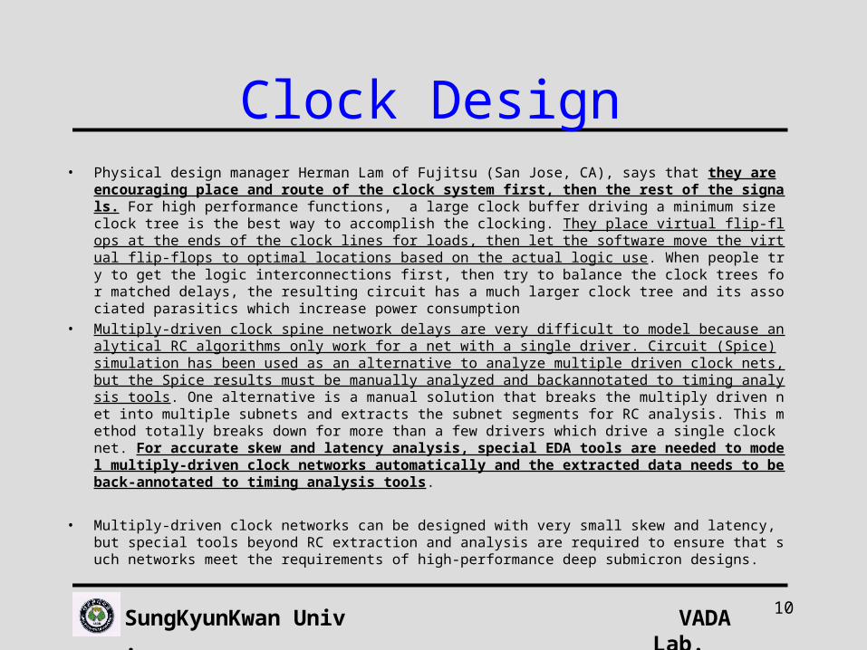
Clock Design• Physical design manager Herman Lam of Fujitsu (San Jose, CA), says that they are encouraging pl
ace and route of the clock system first, then the rest of the signals. For high performance functions, a large clock buffer driving a minimum size clock tree is the best way to accomplish the clocking. They place virtual flip-flops at the ends of the clock lines for loads, then let the software move the virtual flip-flops to optimal locations based on the actual logic use. When people try to get the logic interconnections first, then try to balance the clock trees for matched delays, the resulting circuit has a much larger clock tree and its associated parasitics which increase power consumption
• Multiply-driven clock spine network delays are very difficult to model because analytical RC algorithms only work for a net with a single driver. Circuit (Spice) simulation has been used as an alternative to analyze multiple driven clock nets, but the Spice results must be manually analyzed and backannotated to timing analysis tools. One alternative is a manual solution that breaks the multiply driven net into multiple subnets and extracts the subnet segments for RC analysis. This method totally breaks down for more than a few drivers which drive a single clock net. For accurate skew and latency analysis, special EDA tools are needed to model multiply-driven clock networks automatically and the extracted data needs to be back-annotated to timing analysis tools.
• Multiply-driven clock networks can be designed with very small skew and latency, but special tools beyond RC extraction and analysis are required to ensure that such networks meet the requirements of high-performance deep submicron designs.

SungKyunKwan Univ.
11VADA Lab.
PLL• A phase-locked loop (PLL) is useful to resynchronize clocks and to generate multiples of
the base system clock. The PLL can develop a clock with zero or even negative effective skew by adjusting the phase comparator response. One caveat is that one must monitor the phase jitter and noise associated with the PLL and clock regeneration circuitry. The jitter and synchronization can create repeatable phase relationships within the clock network for continuous signals. However, PLLs consume a lot of power making them less attractive for low power applications.
• According to John Harrington, manager of ASIC products at AT&T Microelectronics (Reading, PA), "PLLs are useful for clock doublers and triplers [and other multiples]. This can help by reducing external clock frequencies and allow lower cost crystals which can normally go up to 40 MHz. Three-fourths of their designs have a PLL to synchronize and or align clock edges. The designer needs to be careful of PLL latency and lock times for those situations where the clock is not continuous."
• Jim Smith, ASIC product manager at Hitachi America (Brisbane, CA), agrees, noting,"We try to add PLLs to compensate and resync the clocks where possible. For multiple clocks, the problem is the latency and lock times for the clocks as well as the added jitter errors. The jitter errors add to the total clock skew."
SungKyunKwan Univ.
12VADA Lab.
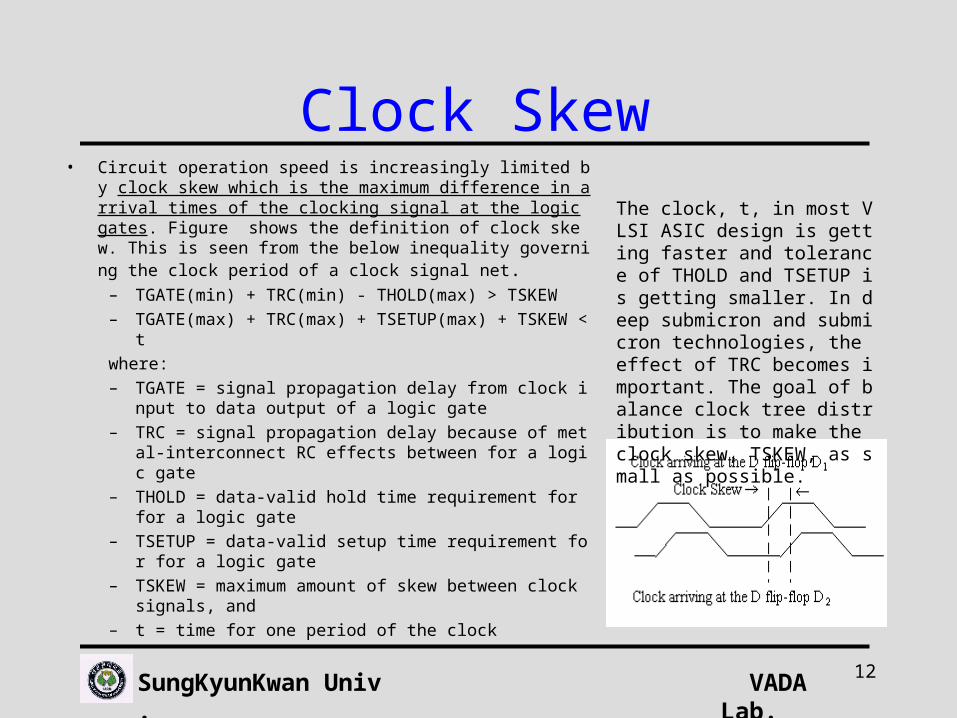
Clock Skew• Circuit operation speed is increasingly limited by clock skew whi
ch is the maximum difference in arrival times of the clocking signal at the logic gates. Figure shows the definition of clock skew. This is seen from the below inequality governing the clock period of a clock signal net.
– TGATE(min) + TRC(min) - THOLD(max) > TSKEW
– TGATE(max) + TRC(max) + TSETUP(max) + TSKEW < t
where:
– TGATE = signal propagation delay from clock input to data output of a logic gate
– TRC = signal propagation delay because of metal-interconnect RC effects between for a logic gate
– THOLD = data-valid hold time requirement for for a logic gate
– TSETUP = data-valid setup time requirement for for a logic gate
– TSKEW = maximum amount of skew between clock signals, and
– t = time for one period of the clock
The clock, t, in most VLSI ASIC design is getting faster and tolerance of THOLD and TSETUP is getting smaller. In deep submicron and submicron technologies, the effect of TRC becomes important. The goal of balance clock tree distribution is to make the clock skew, TSKEW, as small as possible.
SungKyunKwan Univ.
13VADA Lab.
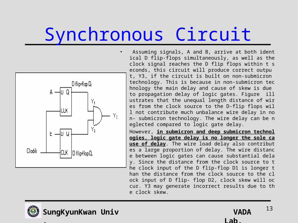
Synchronous Circuit• Assuming signals, A and B, arrive at both identical D flip-fl
ops simultaneously, as well as the clock signal reaches the D flip flops within t seconds, this circuit will produce correct output, Y3, if the circuit is built on non-submicron technology. This is because in non-submicron technology the main delay and cause of skew is due to propagation delay of logic gates. Figure illustrates that the unequal length distance of wires from the clock source to the D-flip flops will not contribute much unbalance wire delay in non- submicron technology. The wire delay can be neglected compared to logic gate delay.
• However, in submicron and deep submicron technologies, logic gate delay is no longer the sole cause of delay. The wire load delay also contributes a large proportion of delay. The wire distance between logic gates can cause substantial delay. Since the distance from the clock source to the clock input of the D flip-flop D1 is longer than the distance from the clock source to the clock input of D flip- flop D2, clock skew will occur. Y3 may generate incorrect results due to the clock skew.

SungKyunKwan Univ.
14VADA Lab.
Balanced Clock Tree• A balanced clock tree distribution is the fundamental requirement for synchronous
systems. It can minimize the clock skew and ensure that the clock signals arriving at any logic gates are within the clock skew specification. A typical balanced clock tree is like a binary tree where all children nodes at the same level have the same distance from the root (parent) node. If the period of time for passing signals down a level is identical for all children nodes, then all children nodes will receive the signal from the root (parent) node at the same instant.
SungKyunKwan Univ.
15VADA Lab.
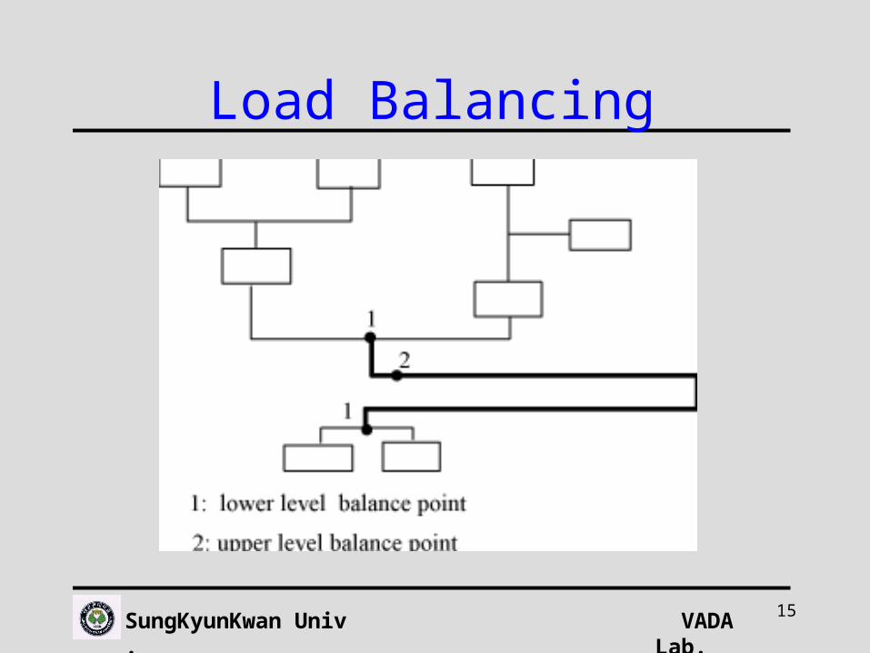
Load Balancing

SungKyunKwan Univ.
16VADA Lab.
Clock Tree Distribution Algorithms
• An optimal balance clock tree distribution is to connect all logic gates directly to the clock source. Assuming that there is no buffer between any logic gate and the clock source, and the wire width is constant, the furthest logic gate will experience the largest delay. The delay time can be equalized for all logic gates by adding logic gate delay and interconnect delay to the faster signal paths. Then all signal paths will experience the same delay. This approach not only has a near zero clock skew, but also has the fastest speed. However, this approach is not feasible because the drive strength of the clock source is limited, and there is not enough room to route wires around the clock source.
• Logic gates are usually being placed by cell placement program at the early stage of layout. The positions of the buffers and the clock source; however, are determined by the clock tree distribution algorithm. Two general clock tree distribution algorithms are discussed here. It should be noted that a few major assumptions are made for the following discussion: the wire resistance and wire capacitance have linear relationship with the clock signal delay; all buffers are identical and they contribute the same delay.

SungKyunKwan Univ.
17VADA Lab.
Clock Tree Distribution• There are other clock tree distribution algorithms proposed, such as buffer distribution
algorithm [3], general zero-skew clock net [4] and process-variation-tolerant zero skew-clock routing [5]. Each algorithm has its own distinct characteristics. It is difficult, if not impossible, to determine which algorithm is the best. If logic gates are evenly distributed, the clock trees generated by these algorithms may look similar. If the placement pattern of the logic gates is unique, clock trees built by different algorithms may have noticeable difference in clock skew, clock signal speed, wire length and design flexibility.

SungKyunKwan Univ.
18VADA Lab.
Elmore Delay

SungKyunKwan Univ.
19VADA Lab.
Buffer Pre-Placement

SungKyunKwan Univ.
20VADA Lab.
Load Balanced Clustering

SungKyunKwan Univ.
21VADA Lab.
Balanced Tree + Mesh

SungKyunKwan Univ.
22VADA Lab.
Single vs. Distributed

SungKyunKwan Univ.
23VADA Lab.
Iso-Radius Buffer Insertion
( a )
( b )( a )
( b )

SungKyunKwan Univ.
24VADA Lab.
Width Control

SungKyunKwan Univ.
25VADA Lab.
Width Tapering

SungKyunKwan Univ.
26VADA Lab.
Interconnect Topology• Resistance ratio = driver resistance / unit wire resistance
• when resistance ratio is small, interconnect topology optimization is importance.
• Importance metric: total wire length, radius (longest source-sink path-length),diameter (for multi-source nets)
• Optimal tree construction algorithms
• BRBC(Bounded-radius bounded-cost) algorithm
• A-tree algorithm: start with a forest of n single-node A-trees, repeatedly
• combining two A-trees into a new one.
SungKyunKwan Univ.
27VADA Lab.
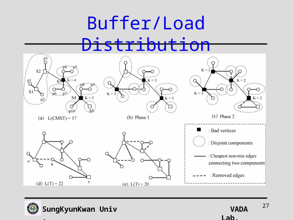
Buffer/Load Distribution

SungKyunKwan Univ.
28VADA Lab.
Hierarchical Matching Tree

SungKyunKwan Univ.
29VADA Lab.
H-Tree
SungKyunKwan Univ.
30VADA Lab.
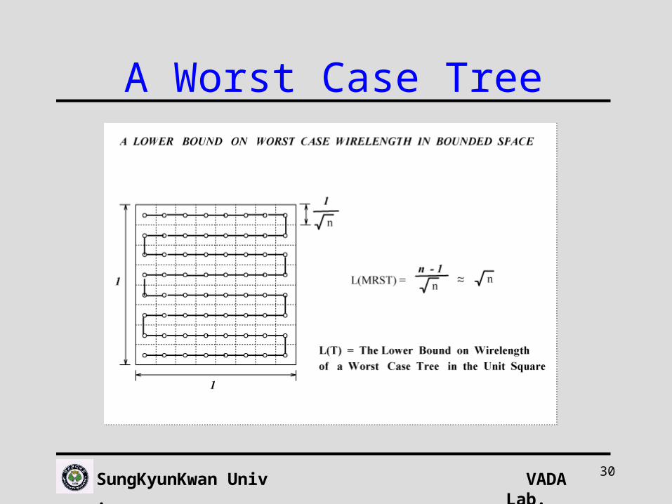
A Worst Case Tree
SungKyunKwan Univ.
31VADA Lab.
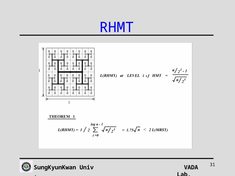
RHMT

SungKyunKwan Univ.
32VADA Lab.
Noise/ SI becoming increasing critical
• Analysis
– Efficient mode for filtering and driver for physical design– Mixture of static/ dynamic analysis tools needed
• Interconnect Planning– Present routing methodology increasingly inadequate– Mixture of planning & constrained synthesis needed– Efficient Noise metrics– Noise avoidance routing– Clocking - managing skew, interconnect vs. device variability– Buffer Insertion - needs to better integrated into design methodolog
y– Use of design guidelines necessary in practice
• Noise/ SI problems are difficult and pervasive, but are TRACTABLE!!!

SungKyunKwan Univ.
33VADA Lab.
Interconnect Scaling• More levels of interconnect packed closer together
• Metal thickness remain constant because of resistance
• In the scaling from 1.8 um to 0.9 um pitch, line-to-line capacitance increases from 46% to 68% of full-loaded self capacitance

SungKyunKwan Univ.
34VADA Lab.
Design Issues for Noise• Reduce coupling noise
• Increase driver strength
• Increase spacing between wires or route signal lines alternately with power or
• ground,
• Constraint-driven routing
• Reducing power supply noise
• Ensure that power grid is sized correctly for the load it is serving to reduce IR drop
• Add on-chip decoupling capacitance to reduce delta-I noise. With increasing use of dynamic circuits, there is less NWELL capacitance on-chip.
• When employing cores, one must be sensitive to the quality of the interconnects which will carry signals between cores and the ASIC portion of the network

SungKyunKwan Univ.
35VADA Lab.
Noise Avoidance

SungKyunKwan Univ.
36VADA Lab.
Interference Graph
Node: nets/segments of nets
Undirected Edges: horizontal constraint
Directed Edges: Vertical Constraints
Edge Weights: Design Rules, Coupling Rules

SungKyunKwan Univ.
37VADA Lab.
Lines between Planes• Ctotal = Cdown+Cup + Cleft + Cright
Cleft Cright
Cdown
Cup
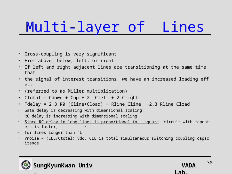
SungKyunKwan Univ.
38VADA Lab.
Multi-layer of Lines
• Cross-coupling is very significant
• From above, below, left, or right
• If left and right adjacent lines are transitioning at the same time that
• the signal of interest transitions, we have an increased loading effect
• (referred to as Miller multiplication)
• Ctotal = Cdown + Cup + 2 Cleft + 2 Cright
• Tdelay = 2.3 R0 (Cline+Cload) + Rline Cline +2.3 Rline Cload• Gate delay is decreasing with dimensional scaling
• RC delay is increasing with dimensional scaling
• Since RC delay in long lines is proportional to L square, circuit with repeaters is faster,
• for lines longer than “L”
• Vnoise = (CLL/Ctotal) Vdd, CLL is total simultaneous switching coupling capacitance

SungKyunKwan Univ.
39VADA Lab.
Transistor Sizing• X is the set (vector) of transistor sizes• Minimize Area(X) subject to Delay(X) <= Tspec
• Minimize Power(X) subject to Delay(X) <= Tspec
valuemin. global unique a has problem Therefore,
paths allfor T X)Pathdelay( T Delay(X)
functiondelay path posynomial x C , x R
RC delay path Each
)l!(posynomia )(
specspec
i1
i
1
n
iixXArea

SungKyunKwan Univ.
40VADA Lab.
Why no perfect solution
x
A
B
C
D
E
Problem with interacting paths
(1) Better to size A than to size all of B,C and D
(2) If X-E is near-critical and A-D is critical,
size A (not D)
False paths, layout considerations not incoporated

SungKyunKwan Univ.
41VADA Lab.
Power-Delay Sizing
• Minimize Power(w)
• subject to Delay(w) <= Tspec
• Area(W) <= Aspec
• Each Gate size >= Minsize
• Minimize dynamic power = minimize CL = minimize all transistor size!
• Right? (unfortunately not!)
circuit designed- wellain power totalof 20%-10 than Less
n time transitio ctance,transcondu
,P f )2(V 12/
P C
T2
dd
T2
L
Tcktshort
dddynamic
VP
fVP

SungKyunKwan Univ.
42VADA Lab.
The Catch• Delay of gate A is large
• Therefore, the value of t for B,C,D,E is large
• Therefore, short ckt power for B,C,D,E is large
• Can be reduced by reducing the delay A (size A!)
A
B
C
D
E

SungKyunKwan Univ.
43VADA Lab.
Low Power Issues• Power optimization allows logic optimization to simultaneously optimize for timing, area and powe
r. So all the inputs to optimization are the same with the addition of two new power constraints: max dynamic power and max leakage power. A power-optimizing logic optimization system takes as input a gate-level netlist or database, technology library, optional constraints for timing and area, and parasitic information (initially in the form of estimated wireloads, but if backannotation has been done that information will be used). All that's needed in addition for power optimization is to set a power constraint and supply switching activity - the same switching activity used with power analysis.
• What you get out of power optimization is a gate-level netlist, optimized to meet all of your constraints. A natural question to ask is: "If optimization at the RTL and Behavioral levels can have a great impact on final power dissipation, why offer a gate-level power optimization capability first?" Over a decade of experience in synthesis and optimization it has proven that RTL level suffers the impact of optimization at the gate level. The first commercially successful synthesis products were gate-level timing optimizers and these paved the way for RTL and Behavioral synthesis systems. In a similar way gate-level power optimization will pave the way for RTL and Behavioral synthesis for low power.
• Earlier we made the point that analysis precedes optimization. Here we make another general point: We might say that just as analysis precedes optimization, optimization precedes synthesis. Or to put it another way: Successful synthesis at higher levels requires successful optimization at lower levels.

SungKyunKwan Univ.
44VADA Lab.
References and Suggested Readings• [1] B. Schweber. Delivering The High-Speed Clock: Not Easy To Be On Time. In Proc. EDN, July 6, 1995
• [2] H. B. Bakoglu. Circuits, Interconnections, and Packaging for VLSI, Addison-Wesley Publishing Company. New York. 1990
• [3] J. D. Cho and M. Sarrafzadeh. A Buffer Distribution Algorithm for High-Performance Clock Net Optimization. In Proc. IEEE Transactions On Very Large Scale Integration (VLSI) Systems, Vol 3, No.1, March 1993N.
• [4] N. C. Chou and C. K. Cheng. On General Zero-Skew Clock Net Construction. In Proc. IEEE Transactions On Very Large Scale Integration (VLSI) Systems, Vol 3, No.1, March 1995
• [5] S. Lin and C. K. Wong. Process-Variation-Tolerant Zero Skew Clock Routing. In IEEE 1993 Custom Integrated Circuits Conference. 1993
• [6] B. Wiederhold. Deep submicron ASIC Design Requires Design Planning. In Proc. EDN, February 16, 1995
• [7] Menezes, A. Balivada, S. Pullela and L. T. Pillage. Skew Reduction in Clock trees Using Wire Width Optimization. In Proc. IEEE 93 Custom Integrated Circuits Conference. 1993
• [8] R. Hansen and R. Deming. ASIC Design Techniques Synchronize Dual Clocks In High-Speed Designs. In Proc. EDN, July 1993
• [9] W. Khan and N. Sherwani. Zero Skew Clock Routing Algorithm For High Performance ASIC Systems.
• [10] K. D. Boese and A. B. Kahng. Zero-Skew Clock Routing Trees With Minimum Wirelength. In IEEE 1992 Custom Integrated Circuits Conference. 1992
• [11] X. M. Xiong, J. Hardin and C. K. Cheng. PAS: A Stand Alone Placement Annotation System For High Speed Designs. In IEEE 1993 Custom Integrated Circuits Conference. 1993
• [12] J. Rubinstein, P. Penfield, and M. A. Horowitz. Signal Delay in RC Tree Networks. In Proc. IEEE Transactions On Computer-Aided Design, Vol. CAD-2, No.3, July 1983