Special-Purpose Digital Circuits - RNBS Web page トッ … CMOS Design, H20/5/2 2 Necessary...
29
Mattausch, CMOS Design, H20/5/2 1 Special-Purpose Digital Circuits • Buffer Circuits • Path-Selector Circuits • Information-Storing Circuits • Trigger Circuits • Multi-Vibrator Circuits • Voltage-Generator Circuits CMOS Logic Circuit Design http://www.rcns.hiroshima-u.ac.jp Link(リンク): センター教官講義ノート の下 CMOS論理回路設計
Transcript of Special-Purpose Digital Circuits - RNBS Web page トッ … CMOS Design, H20/5/2 2 Necessary...

Mattausch, CMOS Design, H20/5/2 1
Special-Purpose Digital Circuits
• Buffer Circuits• Path-Selector Circuits• Information-Storing Circuits• Trigger Circuits• Multi-Vibrator Circuits• Voltage-Generator Circuits
CMOS Logic Circuit Designhttp://www.rcns.hiroshima-u.ac.jp
Link(リンク): センター教官講義ノート の下 CMOS論理回路設計

Mattausch, CMOS Design, H20/5/2 2
Necessary Functions other than Logic Operations
CMOS logic circuits do contain more than only logic gates.
1) Transmission of signals over long interconnection lines or to many receivers
- Buffer (inverting, non-inverting, tri-state)2) Selection of an interconnection for a Signal according to a condition
- Selector (multiplexer, demultiplexer)3) Storing an information for some time
- Flip-flop, latch4) Removing Noise from a Signal
- Trigger circuits5) Generation of Synchronous or Asynchronous Control Signal
- Multi-vibrator circuits (a-stable, bi-stable, mono-stable)6) Generation of other Voltages than VDD or VSS
- Voltage generator circuits

Mattausch, CMOS Design, H20/5/2 3
Buffer Circuits- Increasing the driving capability of a logic
signal for large load capacities- Conventional non-inverting buffers- Inverting buffers- Tri-state buffers
Mattausch, CMOS Design, H20/5/2 4
Reduction of Logic-Gate Fan-Out with a Buffer
The delay of a circuit with large fan-out (i. e. large output load) can be reduced with a buffer, if (k-1)·trex > tbuffer is valid.
NAND-gate withfan-out = k, fan-in = m
m
31
2
m-12
1
3
k
NAND-gate withfan-out = 1, fan-in = m
m
31
2
m-12
1
3
k
Non-inverting Buffer
)k(mm, fexfinNANDdf ttt ⋅+⋅⋅=rexrinNANDdr ttt ⋅+⋅= km,
Delay without buffer
bufferfexfinNANDdf tttt ++⋅⋅= )(mm,
bufferrexrinNANDdr tttt ++⋅= m,
Delay with buffer
Mattausch, CMOS Design, H20/5/2 5
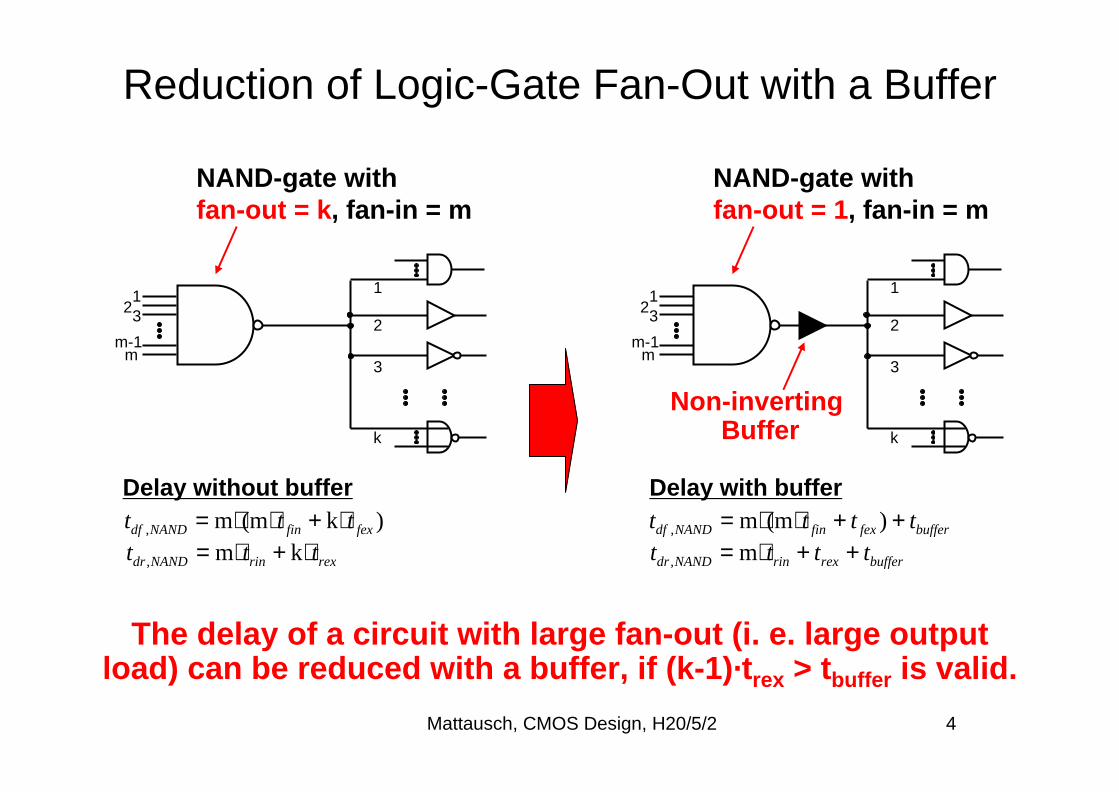
Construction of Non-Inverting CMOS Buffers
Non-inverting buffers have even number of inverters. Each stage has a factor Ani-buffer (Cload,Cin) larger driving capability.
VSS
Cload
VoutVin
Vin
VSS
Cload
Vout
I1 I2 I2N-1 I2N
A 0 Wp
Wn
A1 Wp
Wn
A 2N −2 Wp
Wn
A 2N −1 Wp
Wn
Optimum choice of A and N
N21
1in
loadbufferni C
CA
=−
=−
1in
load21
bufferni C
ClnintN
(Cin1 is the input capacity of the 1st inverter)

Mattausch, CMOS Design, H20/5/2 6
Construction of Inverting CMOS Buffers
Inverting buffers use an odd number of cascaded inverters. Each stage has again Ai-buffer(Cload,Cin) larger driving capability.
VSS
Cload
VoutVin Optimum Choice of A and N
1N21
1in
loadbufferi C
CA
+
−
=
−
=− 2
1
1in
load21
bufferi C
ClnintN
Vin
VSS
Cload
Vout
I1 I2 I2N I2N+1
A 0 Wp
Wn
A1 Wp
Wn
A 2N −1 Wp
Wn
A 2N Wp
Wn
I3
A 2 Wp
Wn
(Cin1 is the input capacity of the 1st inverter)
Mattausch, CMOS Design, H20/5/2 7
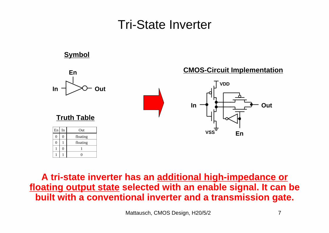
Tri-State Inverter
A tri-state inverter has an additional high-impedance or floating output state selected with an enable signal. It can be
built with a conventional inverter and a transmission gate.
OutIn
Symbol
VDD
En
VSS En
In Out
En In Out
0 0 floating
0 1 floating
1 0 1
1 1 0
Truth Table
CMOS-Circuit Implementation
Mattausch, CMOS Design, H20/5/2 8
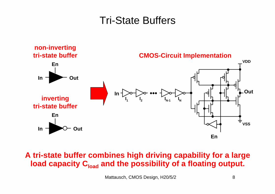
Tri-State Buffers
A tri-state buffer combines high driving capability for a large load capacity Cload and the possibility of a floating output.
non-inverting tri-state buffer
OutIn
En
CMOS-Circuit Implementation
OutIn
En
inverting tri-state buffer
VDD
VSS
En
In OutI1 I2 IN-1 IN

Mattausch, CMOS Design, H20/5/2 9
Path-Selector Circuits - Multiplexer- and Demultiplexer Principles- Implementation with Transmission Gates- Series Connection of Transmission Gates- Implementation with Tri-State Inverters or
Tri-State Buffers

Mattausch, CMOS Design, H20/5/2 10
Multiplexer and Demultiplexer Principles
Conditional signal-path selection is performed with multiplexer- or demultiplexer circuits.
123
N
NDataInputLines
OneSelected
DataOutput
NPossible0utputLines
123
N
OneDataInput
between ln(N) and NControl/Selector Lines
between ln(N) and NControl/Selector Lines
Multiplexer(MUX)
Demultiplexer(DEMUX)

Mattausch, CMOS Design, H20/5/2 11
Circuits
Multiplexer Realization with Transmission Gates
Path-selector realization is easiest by transmission gates.
En
In Out
In Out
En
Transmission Gates 4-Input Multiplexer
En
In Out
In Out
EnEn1 En2 En3 En4
In1
In2
In3
In4
Out
Symbols Minimum Transmission Gates
Minimum Select SignalsEn1 En2
In1
In2
In3
In4
Out

Mattausch, CMOS Design, H20/5/2 12
Series Connection of Transmission Gates
A series connection of N transmission gates represents an RC-chain. Therefore, its delay time increases with N2.
tPS,hl ≈ tPS,lh ≈ Rn || Rp( )Cload( )⋅ N+ 0.35 ⋅ Rn || Rp( )Cinn + Cinp( )⋅ N2
Series of N transmission gates
driving a load
Delay model for a series of N
transmission gates
Delay equation as a function of N
transmission gates
Mattausch, CMOS Design, H20/5/2 13
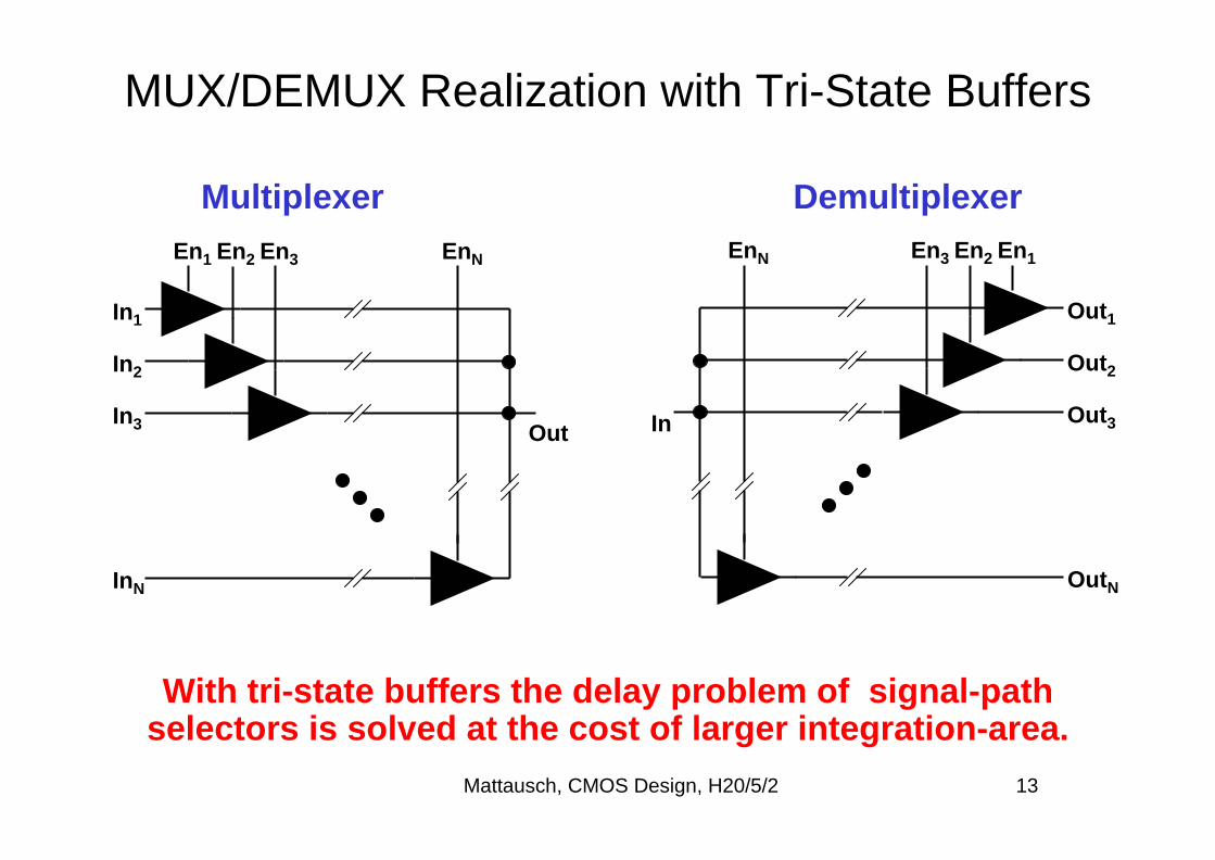
MUX/DEMUX Realization with Tri-State Buffers
With tri-state buffers the delay problem of signal-path selectors is solved at the cost of larger integration-area.
Out
En1 En2 En3 EnN
In1
In2
In3
InN
In
En1En2En3EnN
Out1
Out2
Out3
OutN
Multiplexer Demultiplexer
Mattausch, CMOS Design, H20/5/2 14
Information-Storing Circuits - Stabilizing-Feedback Principle- Set-Reset Flip-Flop- Clocked Flip-Flops
• Level Sensitive Flip-Flops• Edge-Triggered Flip-Flops• Flip-Flop Timing

Mattausch, CMOS Design, H20/5/2 15
Stabilizing-Feedback Principle of Data Storage
By feeding back the identical signal to a circuit node, stable circuit states result, which are usable for data storage.
Q
Stabilizing inverter-feedback coupling
Q
QQStable States
“one”
“zero”
1 0
0 1
Resulting stable circuit states

Mattausch, CMOS Design, H20/5/2 16
Set-Reset (SR) Flip-Flop
Set-reset flip-flops extend the stabilizing feedback principle by a method for external modification of the stored data.
Truth table
QQR
0 1
S
00
1 0
10
11
11
1 0
Q QQ
Circuit diagram (constructed with NAND gates)
QS
R
Logic Symbol
S
R
Q
Q
SR Flip-Flop
Mattausch, CMOS Design, H20/5/2 17
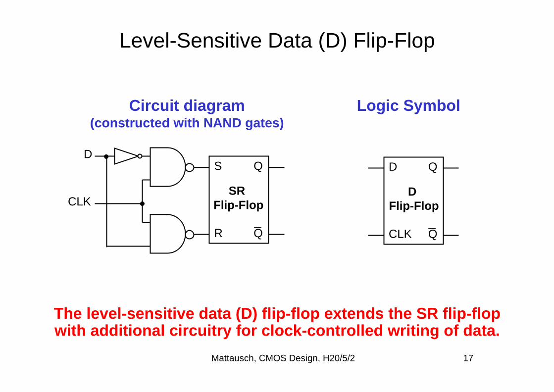
Level-Sensitive Data (D) Flip-Flop
The level-sensitive data (D) flip-flop extends the SR flip-flop with additional circuitry for clock-controlled writing of data.
Circuit diagram (constructed with NAND gates)
DS
R
Q
Q
Logic Symbol
CLK
D
CLK
Q
Q
D Flip-Flop
SR Flip-Flop
Mattausch, CMOS Design, H20/5/2 18
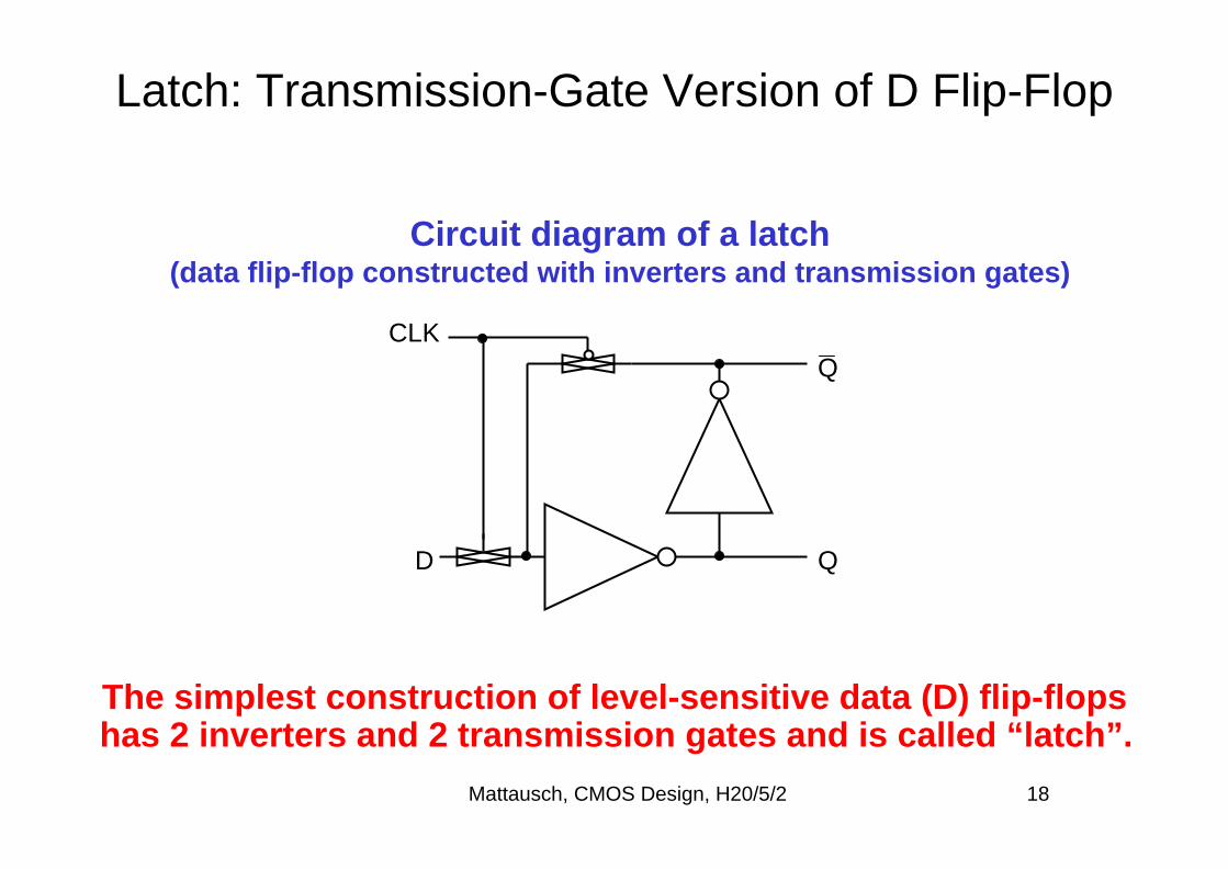
Latch: Transmission-Gate Version of D Flip-Flop
The simplest construction of level-sensitive data (D) flip-flops has 2 inverters and 2 transmission gates and is called “latch”.
Circuit diagram of a latch (data flip-flop constructed with inverters and transmission gates)
D
CLK
Q
Q

Mattausch, CMOS Design, H20/5/2 19
Edge-Triggered data (D) Flip-Flop
The edge-triggered D flip-flop has 2 latches. Data transfer to the slave latch occurs only at transition edges of the clock.
Circuit diagram of a D flip-flop into which data is written at the positive edge (low-high) change of the clock
(constructed with 2 latches)
Q
Q
D
CLK
Master Latch Slave Latch
Mattausch, CMOS Design, H20/5/2 20
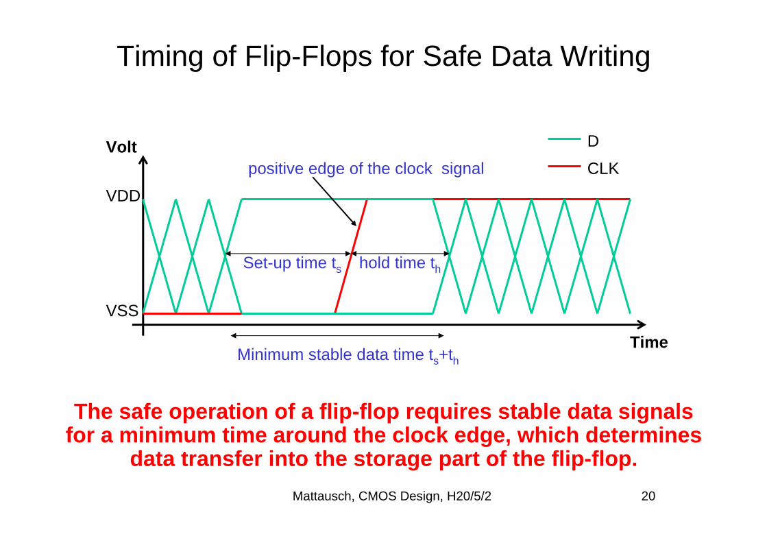
Timing of Flip-Flops for Safe Data Writing
The safe operation of a flip-flop requires stable data signals for a minimum time around the clock edge, which determines
data transfer into the storage part of the flip-flop.
Time
Volt
VDD
VSS
D
CLK
Set-up time ts hold time th
Minimum stable data time ts+th
positive edge of the clock signal

Mattausch, CMOS Design, H20/5/2 21
Trigger Circuits - Removal Possibilities of Signal Noise - Schmitt-Trigger Circuit

Mattausch, CMOS Design, H20/5/2 22
Signal Noise and Removal Possibilities
Noise can be removed from a signal with a circuit who has different switching points for low-high and high-low transition.
Time
No
ise-
Rem
ova
l C
ircu
it In
pu
tVDD
VSS
High-Switching PointVSPH
VDD
VSS
No
ise-
Rem
ova
l C
ircu
it O
utp
ut
Time
Inverting Removal Circuit Assumed
VDD
Ou
tpu
t V
olt
age
VDDVSS
VSS
Input Voltage
VSPL VSPH
Low-Switching PointVSPL
Desired Switching-PointCharacteristic of Circuit
Mattausch, CMOS Design, H20/5/2 23
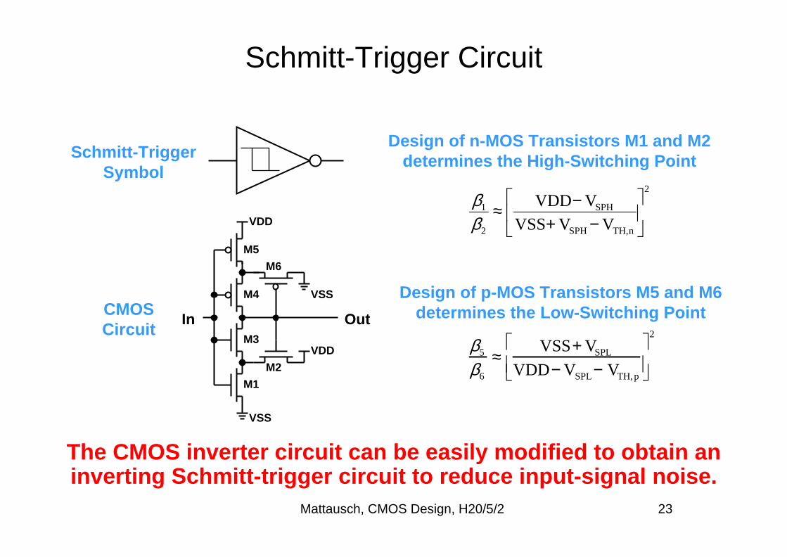
Schmitt-Trigger Circuit
The CMOS inverter circuit can be easily modified to obtain an inverting Schmitt-trigger circuit to reduce input-signal noise.
VDD
VSS
Out
VDD
VSS
In
M1
M3
M2
M6
M4
M5
2
nTH,SPH
SPH
2
1
VVVSS
VVDD
−+−≈
ββ
β5
β6
≈VSS+ VSPL
VDD− VSPL− VTH, p
2
Schmitt-TriggerSymbol
CMOSCircuit
Design of n-MOS Transistors M1 and M2 determines the High-Switching Point
Design of p-MOS Transistors M5 and M6 determines the Low-Switching Point
Mattausch, CMOS Design, H20/5/2 24
Multi-Vibrator Circuits - Destabilizing-Feedback Principle- A-Stable Multi-Vibrator or Oscillator- Bi-Stable Multi-Vibrator or Flip-Flop
(see Part on Information-Storing Circuits)- Mono-Stable Multi-Vibrator

Mattausch, CMOS Design, H20/5/2 25
Destabilizing Feedback: Oscillator Circuits
By feeding back the inverted signal to a circuit node, an unstable state is occurs, which is used for oscillator circuits.
Destabilizing inverter-feedback coupling
Resulting unstable (oscillating) signals at circuit nodes
Q1Q2
Q3
Qi
VDD
Time
VSS
Mattausch, CMOS Design, H20/5/2 26
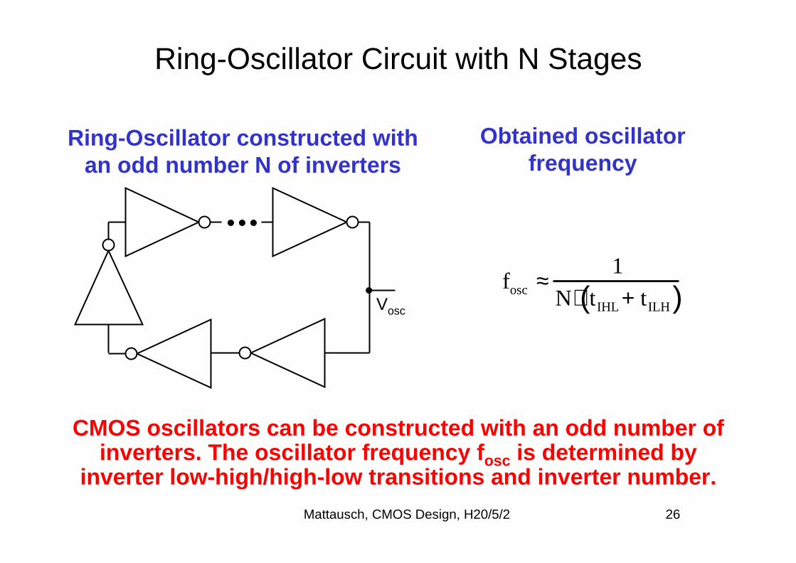
Ring-Oscillator Circuit with N Stages
CMOS oscillators can be constructed with an odd number of inverters. The oscillator frequency fosc is determined by
inverter low-high/high-low transitions and inverter number.
Ring-Oscillator constructed with an odd number N of inverters
Obtained oscillator frequency
Vosc
fosc ≈1
N⋅ tIHL + tILH( )
Mattausch, CMOS Design, H20/5/2 27
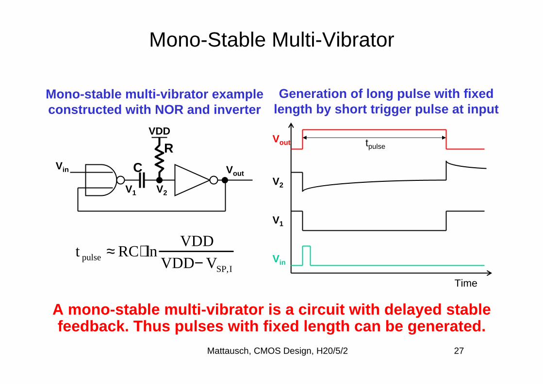
Mono-Stable Multi-Vibrator
A mono-stable multi-vibrator is a circuit with delayed stable feedback. Thus pulses with fixed length can be generated.
VDD
Time
V1 V2
VoutC
RVin
Vin
V1
V2
Vout
Mono-stable multi-vibrator example constructed with NOR and inverter
Generation of long pulse with fixed length by short trigger pulse at input
t pulse ≈ RC⋅ lnVDD
VDD− VSP,I
tpulse
Mattausch, CMOS Design, H20/5/2 28
Voltage-Generator Circuits
Mattausch, CMOS Design, H20/5/2 29
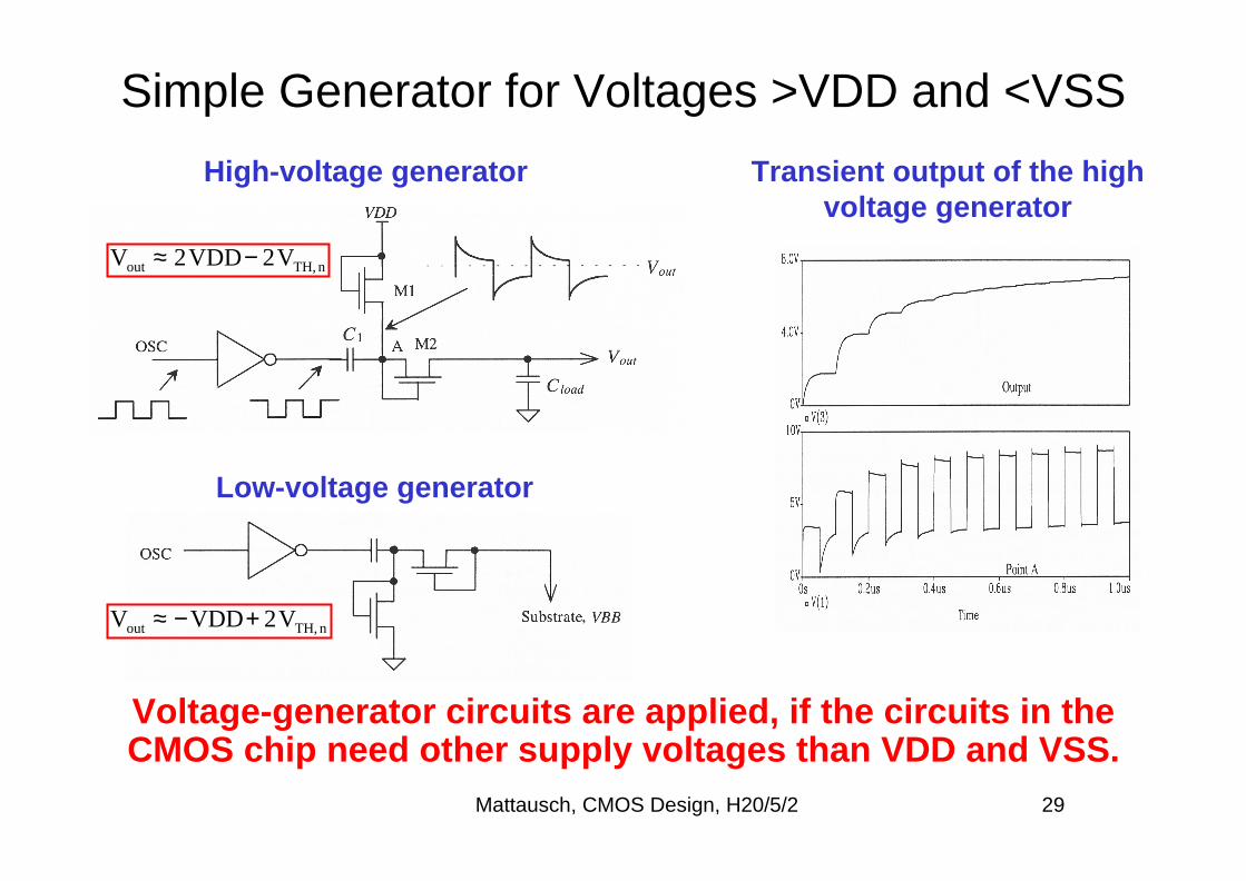
Simple Generator for Voltages >VDD and <VSS
Voltage-generator circuits are applied, if the circuits in the CMOS chip need other supply voltages than VDD and VSS.
High-voltage generator Transient output of the high voltage generator
Low-voltage generator
Vout ≈ 2VDD− 2VTH, n
Vout ≈ −VDD+ 2VTH, n