OpticalTransmitterfor Ultra-WideBandSignals Ultra-WideBandSignals ... in chapter 2 by presenting the...
80
Optical Transmitter for Ultra-Wide Band Signals Rodrigo Silva Maciel Faculdade de Ciências Universidade do Porto A dissertation submitted for the degree of Master in Physical Engineering Porto 2012
Transcript of OpticalTransmitterfor Ultra-WideBandSignals Ultra-WideBandSignals ... in chapter 2 by presenting the...

Optical Transmitter forUltra-Wide Band Signals
Rodrigo Silva MacielFaculdade de CiênciasUniversidade do Porto
A dissertation submitted for the degree ofMaster in Physical Engineering
Porto 2012

Jury:
President Prof. António Manuel Pais Pereira LeiteExternal Examiner Prof. Luís Filipe Mesquita Nero Moreira AlvesSupervisor Prof. Henrique Manuel C. F. SalgadoCo-supervisor Prof. José A. Machado da Silva

“Let the future tell the truth and evaluate each one according to his workand accomplishments. The present is theirs; the future, for which I
have really worked, is mine.”
Nikola Tesla


Acknowledgements
First, I would like to thank my parents, Alípio and Gracinda, and mygirlfriend Tânia for their invaluable support and patience throughout thetime I have been enrolled with this work.
I would also like to thank my supervisors, Prof. Henrique Salgado andProf. José Machado da Silva, for their priceless help in the technical fieldwithout which this work would have been much harder to complete.
I also wish to thank everybody who has been with me during this time atINESC TEC - UTM, namely Dr. Luís Pessoa, Dr. João Oliveira, MárioPereira and Nuno Sousa for all the important and productive discussionsabout this project. Thanks also to Nuno Sousa for providing me theMatlab files necessary for running the VCSEL’s simulations.
Without you all, this work would not have been possible.

Abstract
In this work, the design of an optical transmitter for Ultra-Wide Band(UWB) signals in the 3.168-3.696 GHz frequency range is presented. Twodifferent approaches have been addressed in this work. First, a discretelow-noise amplifier based on commercial off-the-shelf components (COTS)is described. An application-specific design of an integrated circuit is alsodiscussed. This has been achieved using a combination of electronic designautomation (EDA) software. The MOS process used in the integrationstage is an IBM 130 nm, a suitable process for the desired application.
An introduction to the motivations for designing such a transmitter aswell as the need for the use of such wide band signals is presented. UWBis a wireless technology offering high data-rates and providing noise-likesignals. However, it has a short range which can be extended throughthe use of fiber technology. The goal of this work concerns the design ofa suitable electro-optic converter for UWB-over-fiber systems. As such,radio-over-fiber technology is presented and UWB is also discussed. The-oretical descriptions are made throughout, including the diode laser dy-namic operation models and the techniques used to design both versionsof the transmitter based on the desired performance. Specific issues ateach different design stage are also addressed.
These techniques are then applied to the design of the optical transmit-ter, allowing one to obtain most of its properties in order to assess itsperformance under real-life scenarios. An estimated maximum range of31 meters is found for the discrete version, in combination with a high gainand low overall noise figure. The integrated circuit also presents these fea-tures and it is, as intended, capable of delivering a small dimension andsimple structure device suitable for a wide range of applications.

Resumo
Neste trabalho é apresentado o projecto de um transmissor óptico parasinais de banda ultra-larga (UWB) na gama de frequências de 3.168 -3.696 GHz. Foram projectadas duas versões diferentes deste transmissor.Primeiro é descrito um amplificador de baixo ruído baseado em compo-nentes discretos e comerciais. Depois, é discutida a implementação deuma versão em circuito integrado. Estes dispositivos foram projectadosusando uma combinação de software EDA. Na integração o processo MOSutilizado é o IBM 130 nm, pois apresenta as características apropriadaspara o uso pretendido.
É apresentada uma introdução às motivações de implementar um trans-missor óptico e a necessidade de utilizar tais sinais de banda larga. UWBé uma tecnologia sem fios que permite grandes taxas de transferência dedados e com um comportamento semelhante a ruído. No entanto, apre-senta um curto alcance que pode ser aumentado utilizando fibras ópticas.O objectivo deste trabalho prende-se com o projecto de um conversorelectro-óptico capaz de ser utilizado em sistemas UWB-sobre-fibra. As-sim, a tecnologia rádio-sobre-fibra é discutida bem como as característicasdos sinais UWB. Diversas descrições teóricas são feitas ao longo deste tra-balho, incluindo os modelos de funcionamento dinâmico dos díodos laser eas técnicas utilizadas para projectar cada uma das versões deste transmis-sor baseadas nas características desejadas. Desafios particulares relativosao projecto de cada versão também são discutidos.
Estas técnicas são depois aplicadas ao projecto do transmissor óptico,permitindo obter as suas propriedades de forma a avaliar o seu comporta-mento em situações reais. Um alcance máximo de 31 metros foi estimadopara o dispositivo com componentes discretos, bem como um alto ganhoe uma figura de ruído total baixa. O circuito integrado também apresentaestas características e é, como pretendido, capaz de originar um disposi-tivo final de pequenas dimensões e estrutura simples, adequado para umvasto leque de aplicações.


Contents
1 Introduction 11.1 Background and Motivation . . . . . . . . . . . . . . . . . . . . . . . 11.2 Thesis Organization . . . . . . . . . . . . . . . . . . . . . . . . . . . . 31.3 Contributions . . . . . . . . . . . . . . . . . . . . . . . . . . . . . . . 3
2 Electro-Optic Converter for RoF Applications 52.1 Introduction . . . . . . . . . . . . . . . . . . . . . . . . . . . . . . . . 52.2 Optical Systems for RF Signal Transmission (Radio-over-Fiber) . . . 52.3 UWB Signals . . . . . . . . . . . . . . . . . . . . . . . . . . . . . . . 72.4 VCSEL . . . . . . . . . . . . . . . . . . . . . . . . . . . . . . . . . . 9
2.4.1 Structure and Properties . . . . . . . . . . . . . . . . . . . . 92.4.2 Model . . . . . . . . . . . . . . . . . . . . . . . . . . . . . . . 102.4.3 Small Signal VCSEL Response . . . . . . . . . . . . . . . . . . 122.4.4 Relative Intensity Noise . . . . . . . . . . . . . . . . . . . . . 13
2.5 Summary . . . . . . . . . . . . . . . . . . . . . . . . . . . . . . . . . 14
3 Design of RF Amplifiers 163.1 Introduction . . . . . . . . . . . . . . . . . . . . . . . . . . . . . . . . 163.2 Techniques for Designing Discrete RF Amplifiers . . . . . . . . . . . . 163.3 Integration Using a MOS Process . . . . . . . . . . . . . . . . . . . . 21
3.3.1 Analogue Microelectronics Theory . . . . . . . . . . . . . . . . 213.4 Summary . . . . . . . . . . . . . . . . . . . . . . . . . . . . . . . . . 24
4 Design of the Optical Transmitter for a 3.168-3.696 GHz UWB Sig-nal 254.1 Introduction . . . . . . . . . . . . . . . . . . . . . . . . . . . . . . . . 254.2 General Structure of the Transmitter . . . . . . . . . . . . . . . . . . 264.3 Properties of the Amplifier . . . . . . . . . . . . . . . . . . . . . . . . 26
4.3.1 Frequency Stability . . . . . . . . . . . . . . . . . . . . . . . . 26
i
4.3.2 Gain . . . . . . . . . . . . . . . . . . . . . . . . . . . . . . . . 284.3.3 Noise Figure . . . . . . . . . . . . . . . . . . . . . . . . . . . . 29
4.4 Transistors’ Biasing Network Design . . . . . . . . . . . . . . . . . . 294.5 VCSEL Biasing Network Design . . . . . . . . . . . . . . . . . . . . . 314.6 Design of the Impedance Matching Circuits . . . . . . . . . . . . . . 334.7 MOS Process . . . . . . . . . . . . . . . . . . . . . . . . . . . . . . . 354.8 Design of the IC Transmitter . . . . . . . . . . . . . . . . . . . . . . 354.9 Summary . . . . . . . . . . . . . . . . . . . . . . . . . . . . . . . . . 37
5 Implementation and Simulation of the Optical Transmitter 395.1 Introduction . . . . . . . . . . . . . . . . . . . . . . . . . . . . . . . . 395.2 Implementation in ADS™ . . . . . . . . . . . . . . . . . . . . . . . . 405.3 ADS™ Simulation Results . . . . . . . . . . . . . . . . . . . . . . . . 41
5.3.1 S-Parameters . . . . . . . . . . . . . . . . . . . . . . . . . . . 415.3.2 Noise Figure . . . . . . . . . . . . . . . . . . . . . . . . . . . . 435.3.3 Non-Linear Distortion . . . . . . . . . . . . . . . . . . . . . . 445.3.4 Error Vector Magnitude (EVM) . . . . . . . . . . . . . . . . . 46
5.4 Integration using the IBM 130 nm MOS Process with Cadence™ . . . 495.5 Cadence™ Simulation Results . . . . . . . . . . . . . . . . . . . . . . 50
5.5.1 S-Parameters . . . . . . . . . . . . . . . . . . . . . . . . . . . 505.5.2 Noise Figure . . . . . . . . . . . . . . . . . . . . . . . . . . . . 515.5.3 Non-Linear Distortion . . . . . . . . . . . . . . . . . . . . . . 52
5.6 Layout of the Integrated Circuit using Cadence™ . . . . . . . . . . . 535.7 Summary . . . . . . . . . . . . . . . . . . . . . . . . . . . . . . . . . 56
6 Conclusion 57
References 59
A Power Relation Between Spurious and Fundamental ComponentsThrough Intermodulation Distortion 62
B Free-Space Path Loss 64
ii

List of Figures
1.1 Typical setup of an optical transmitter for UWB signals in Radio-over-Fiber systems. . . . . . . . . . . . . . . . . . . . . . . . . . . . . . . . 2
2.1 General scheme of a RoF system [1]. . . . . . . . . . . . . . . . . . . 62.2 Band structure of UWB spectrum. . . . . . . . . . . . . . . . . . . . 82.3 General VCSEL structure, indicating the active region’s length (La) [2]. 92.4 VCSEL equivalent circuit of the laser parasitics. . . . . . . . . . . . . 122.5 Small signal transfer function of the VCSEL. . . . . . . . . . . . . . . 13
3.1 Schematic diagram of a 2-port network. . . . . . . . . . . . . . . . . . 173.2 Diagram of a typical amplifier, including a transistor and its corre-
sponding source and load matching circuits. . . . . . . . . . . . . . . 183.3 Matching circuit using stubs: L is the length of the stub and d is its
length position along the transmission line. . . . . . . . . . . . . . . . 203.4 Microstrip line model: d is the thickness of the substrate with εr per-
mittivity and W is the width of the line [3]. . . . . . . . . . . . . . . 203.5 Small-signal equivalent circuit model of a FET when considering the
channel-length modulation effect and some intrinsic capacitances. . . 223.6 Input impedance matching scheme used. . . . . . . . . . . . . . . . . 233.7 Bondpad and bonding wire model. . . . . . . . . . . . . . . . . . . . 23
4.1 General scheme of the transmitter to be designed. . . . . . . . . . . . 264.2 Stability circles for the amplifier at 4 GHz with the used reflection
coefficients. . . . . . . . . . . . . . . . . . . . . . . . . . . . . . . . . 274.3 Scheme of the biasing network used to bias both transistors (T1 and
T2 are the λ/4 transmission lines). . . . . . . . . . . . . . . . . . . . . 304.4 Biasing network for the VCSEL. . . . . . . . . . . . . . . . . . . . . . 324.5 Frequency response of the VCSEL biasing circuit and parasitics. . . . 334.6 Schematic representation of an implemented matching network using
a short-circuited stub. . . . . . . . . . . . . . . . . . . . . . . . . . . 33
iii

4.7 Simplification made to the matching networks between the first andthe second transistor. . . . . . . . . . . . . . . . . . . . . . . . . . . . 34
5.1 Schematic of the LNA and the VCSEL biasing circuit in ADS™. . . . 405.2 Magnitude and phase of the S21 and S11 parameters of the LNA. . . . 435.3 Simulated noise figure of the LNA. . . . . . . . . . . . . . . . . . . . 445.4 Linear (red) and compression curve (blue) of the LNA. . . . . . . . . 455.5 UWB signal spectra after several transmission stages for an input
power of -30 dBm. . . . . . . . . . . . . . . . . . . . . . . . . . . . . 465.6 Simulation setup used for the EVM simulations. . . . . . . . . . . . . 475.7 Transmitter EVM results for different input power values. . . . . . . . 485.8 Constellation diagrams of the UWB signal after passing through the
optical transmitter, using different input powers. . . . . . . . . . . . . 485.9 Schematic of the circuit used for simulations, made with Cadence™. . 495.10 Magnitude and phase of the S21 parameter and magnitude of the S11
parameter of the circuit implemented with Cadence™. . . . . . . . . 515.11 Noise figure of the LNA. . . . . . . . . . . . . . . . . . . . . . . . . . 525.12 Compression curve and 1 dB compression point of the LNA. . . . . . 535.13 Layout of the components making the IC. . . . . . . . . . . . . . . . 545.14 One of the transistors designed, where the stacked layout technique
can be observed. . . . . . . . . . . . . . . . . . . . . . . . . . . . . . 55
A.1 Input-to-output power characteristics of a non-linear system. . . . . . 62
iv
List of Tables
2.1 Different modulation schemes and coding rates used for obtaining theseveral data rates defined for UWB signals [4]. . . . . . . . . . . . . 8
2.2 Laser parameters used. . . . . . . . . . . . . . . . . . . . . . . . . . . 112.3 Values of the parasitic components. . . . . . . . . . . . . . . . . . . . 12
4.1 Values of the components used in the biasing network. . . . . . . . . 304.2 Values of the components of the VCSEL biasing network. . . . . . . . 324.3 Dimensions of the transmission lines (TL) and stubs (S) used in the
matching networks 1, 2 and 3 of figure 4.1. For example, the length ofthe first line of the matching network 2, TL2,1, is 143.5 mil. . . . . . . 35
4.4 Values of the components of the IC biasing network. . . . . . . . . . . 364.5 Values of the electrical components used for the VCSEL biasing net-
work in the IC. . . . . . . . . . . . . . . . . . . . . . . . . . . . . . . 37
5.1 UWB signal parameters chosen for simulation purposes. . . . . . . . . 415.2 Third-order intercept points and SFDR of the transmitter. . . . . . . 445.3 1 dB compression points. . . . . . . . . . . . . . . . . . . . . . . . . . 455.4 Input and output-referred third-order intercept points for the circuit
implemented using Cadence™. . . . . . . . . . . . . . . . . . . . . . . 525.5 Input and output-referred 1 dB compression points for the circuit im-
plemented using Cadence™. . . . . . . . . . . . . . . . . . . . . . . . 53
v

List of Acronyms
ADS™ Advanced Design System™BER Bit Error RateBS Base StationBSs Base StationsCOTS Commercial Off-the-ShelfCS Central StationDC Direct CurrentDCM Dual Carrier ModulationEVM Error Vector MagnitudeFEC Forward Error CorrectionFET Field-Effect TransistorIC Integrated CircuitIIP3 Input-referred Third-order Intercept PointILD Intrinsic Laser DiodeIMD Intermodulation DistortionIO Input-to-OutputLNA Low-Noise AmplifierMOS Metal-Oxide-SemiconductorOFDM Orthogonal Frequency Division MultiplexingOIP3 Output-referred Third-order Intercept PointPCB Printed Circuit BoardQ Factor Quality FactorQPSK Quadrature Phase Shift KeyingRF Radio-FrequencyRIN Relative Intensity NoiseRoF Radio-over-FiberTFC Time Frequency CodeUWB Ultra-Wide BandVCSEL Vertical-Cavity Surface-Emitting Laser
vi

Chapter 1
Introduction
1.1 Background and MotivationUltra-Wide Band (UWB) is an emergent technology with deep expected impact on 4thgeneration wireless communication systems. It can be simply defined as any wirelesstransmission setup that uses a bandwidth of at least 500 MHz in between the 3.1-10.6GHz frequency range and a maximum power spectral density of 75 nW/MHz (-41.3dBm/MHz) [5]. The main advantages of this technology are its reduced complexityand low power consumption, making it suitable for use in commercial wide-bandsystems, as for example in Wireless Personal Area Networks (WPAN).
UWB signals can be generated using one of three different approaches: shortpulses, Orthogonal Frequency Division Multiplexing (OFDM) or Code Division Mul-tiple Access (CDMA) [6]. Either one will generate the large bandwidths necessaryfor this technology, so the choice of which one to use has to be made according tothe desired application requirements, the complexity of the devices and power con-sumption restrictions. UWB allows for several different data rates, ranging from 53.3Mb/s to 480 Mb/s. However, a higher data rate usually means a lower range, beingjust a few meters for its highest rate [4].
With all of these important characteristics, it is clear that UWB is a promisingtechnology for future services where high data rates are needed and short range is notan issue. However, if the advantages provided by UWB signals are desired but longeroperating distances are also sought, UWB alone might not be enough - other waysof utilizing these high data rate signals over longer distances need to be investigated.In this way this promising technology can be further applied to a larger variety ofapplications to suit tomorrow future needs. One such specific case is the recentproposal of UWB technology in the next generation access networks [7].
1

In this work, we are interested in the investigation of fiber supported UWB signaltransmission in order to extend the technology’s range - the so-called Radio-over-Fiber (RoF) technology. Specifically, the goal is to design an optical transmitter basedon MOS (Metal-Oxide-Semiconductor) technology, capable of operating with UWBsignals in the 3.168-3.696 GHz frequency range, by using a vertical-cavity surface-emitting laser (VCSEL). This is carried out by first designing and studying a discrete(PCB-supported) version of the transmitter, followed by its integration using thechosen MOS process. The importance of using a MOS process is due to its abilityto deliver very small devices at a cost that might become low enough for them tobe used in a widespread manner. The typical setup of optical transmitters in RoFsystems using UWB signals can be seen in figure 1.1.
Photodetector
Wireless Link Optical
Fiber
PO
Ib
G
Is
IRX
L
UWBTX
UWBRX
Amplifier VCSEL
Optical Transmitter
Figure 1.1: Typical setup of an optical transmitter for UWB signals in Radio-over-Fiber systems.
Although a VCSEL integrated circuit driver, specifically for UWB signals in thisfrequency range, has never been designed to the best of our knowledge, there are nowa-days some drivers that are capable of delivering high data throughput (10 Gb/s perVCSEL channel) at a relatively low cost using either a 90 nm [8] or a 130 nm [9] CMOStechnology. The former achieves 10 Gb/s by implementing a 4-PAM (Pulse AmplitudeModulation) scheme with equalization in order to compensate for modal dispersion inmulti-mode fibers. The latter uses auto-power control and auto-modulation control toobtain constant optical power outputs over a 4-channel VCSEL array, and an activefeedback technique for bandwidth improvement. Other examples of VCSEL driversfor multi-Gb/s data rates exist, just like the one detailed in [10].
A complete RoF system for optically transmitting and wirelessly receiving 1.44Gb/s UWB signals in the 60 GHz band has also been proposed [11] for integrated fiber-to-the-home and WPAN connectivity, employing two different modulation schemes.Specifically, the VCSEL used in the transmitting end (composed of an amplifier, abias-T and a 1550 nm VCSEL) is directly modulated by the UWB signal, with fre-quency up-conversion to the 60 GHz being made through a Mach-Zehnder modulator.
2
These signals are then distributed using optical fiber to the remote sites where theyare wirelessly transmitted to a 60 GHz receiver. This receiver will then amplify, filterand down-convert the signal for analysis. Such high data rates were demonstratedfor a RoF transmission using a 40 km-long fiber plus 5 m wireless transmission.
1.2 Thesis OrganizationAfter this preliminary introduction chapter, which states the motivations for the de-velopment of this project and the main goals to be achieved, the thesis will continuein chapter 2 by presenting the Radio-over-Fiber technology, a mix between opticaland wireless networks, since this is the main application for the optical transmit-ter. In this same chapter, an introduction to VCSEL laser diodes is presented, theirproperties and theoretical model are given and the basic set of rate equations areexplained. Furthermore, an important type of noise generated in laser diodes, therelative intensity noise (RIN), is also discussed since it is also modelled in the systemsimulations.
In chapter 3 the design steps of the optical transmitter are detailed after a firstglimpse on the main RF amplifier design techniques, such as the steps to correctlycreate the discrete low-noise amplifier (LNA), the VCSEL biasing networks and thematching circuits using transmission lines. Also in this chapter, the techniques forintegrating this transmitter using a MOS process are explained, taking into consider-ation the particularities it presents when compared to the discrete device.
In chapter 4, both versions are actually designed to present the desired perfor-mance and their main properties are calculated using the aforementioned techniques.
The thesis proceeds by presenting and explaining, in chapter 5, the simulationresults obtained using several different software tools. These results refer to thesame properties of both designs of the optical transmitter, allowing one to verify thepreviously calculated values and to infer on their implications.
In chapter 6 a final conclusion to this thesis is made and future work possibilitiesare presented.
1.3 ContributionsThe work developed in this thesis yielded some contributions related not only to itsfinal results but also to the methods employed to achieve them. Specifically, thecontributions are as follows:
3
• Development of a co-simulation environment to perform simulations using bothADS™ and Matlab™ where the presented EVM simulations have been per-formed;
• Development of an algorithm to simulate the RIN effects of the VCSEL on thetransmitting signal (in collaboration with Nuno Sousa and UTM staff); and,
• Design of a low complexity and low size optical transmitter for UWB signalsin the 3.168-3.696 GHz frequency range, both in discrete and integrated circuitversions, presenting an estimated large range, high gain and low overall noisefigure.
The work also resulted in one article accepted for presentation at a conference:
• R. S. Maciel, N. Sousa, H. M. Salgado, J.M.B. Oliveira and J. A. M. da Silva,“Optical Transmitter for Ultra-Wide Band signals in the 3.168-3.696 GHz Fre-quency Range”. Conference on Design of Circuits and Integrated Systems(DCIS), November 2012.
4

Chapter 2
Electro-Optic Converter for RoFApplications
2.1 IntroductionThis chapter deals with the optoelectronic components and optical communicationsystems of concern in this work, namely the VCSEL and RoF systems.
Specifically, the next section details the main characteristics, advantages and dis-advantages of systems which integrate in the same network optical and wireless el-ements - the Radio-over-Fiber technology, which could solve some of the problemscurrently faced by the users and providers of high data-rate indoor services.
Also, additional details about UWB signals are given, such as their operatingfrequency, modulation schemes and types of codes used.
The chapter continues by presenting the general structure and main propertiesof a VCSEL, followed by the small signal frequency response of this type of laserdiodes and by the model to be used in the simulations of the transmitter. Here, therate equations and the VCSEL’s equivalent electrical circuit are explained. Also, theorigin and main features of the relative intensity noise are given so that it can be alsoincluded in the simulations to provide for more reliable results.
The chapter ends with a brief summary of the topics and the main features ad-dressed.
2.2 Optical Systems for RF Signal Transmission(Radio-over-Fiber)
Radio-over-Fiber (RoF) is a technology which involves the integration of wireless andfiber optic networks, usually by using fiber optics to distribute a RF signal from a
5

central station (CS) to a base station (BS), which is then responsible for emittingthe signal to mobile stations (MS). Its main objectives are to increase indoor wirelesscoverage for a variety of different technologies (UWB, GSM, UMTS, Wireless LAN,etc) and to reuse wavelengths for high data throughput services [12].
With the ongoing increment of services which need large bandwidths and therising number of their users, the number of BSs will also need to increase in orderto meet the demand and, so, it could become imperative that these BSs be simpleand low cost. Therefore, in RoF the signal routing and processing functions (such ascarrier modulation, frequency conversion, multiplexing) could be only performed atthe CS, depending on the architecture used, making it possible for the BS to simplytake care of signal amplification, optoelectronic conversion and wireless distribution[1]. A general scheme of a RoF system is depicted in figure 2.1 and it can be notedthat the proposed transmitter scheme in figure 1.1 can be viewed as the part ofthe BS responsible for the wireless signal pre-amplification and electrical-to-opticalconversion in the uplink.
Figure 2.1: General scheme of a RoF system [1].
One of the immediate advantages of this technology is the use of optical fibers todistribute the signals, because they present low attenuation losses at currently usedcommunication wavelengths (0.3 dB/km for 1550 nm and 0.5 dB/km for 1310 nm[13]). Other advantages involve the significantly large bandwidth offered by opticalfibers - a very important parameter if the number of BSs increases significantly -as well as their immunity to electromagnetic interference, light weight and smallersizes when compared to other communication systems, whereas the centralized con-figuration allows for simpler maintenance and lower costs [1]. However, as this isfundamentally an analogue transmission system, it also presents some disadvantages.
6
These are related to noise introduction, for example the photodiode noise and thediode laser’s Relative Intensity Noise (RIN, see subsection 2.4.4), and distortion ofthe transmitted signals by the system’s components, caused for example by the non-linear distortion of the laser [13].
There are several types of network architectures that can be used in RoF systemsand whose main differences are related to the frequency bands used to modulate theoptical carriers and distribute the signals from the CS to the BSs. These frequencybands are: base band (BB), intermediate frequency (IF) and radio frequency (RF)[14], making each architecture present its own advantages and disadvantages whenemployed in RoF systems. For example, BB-over-Fiber architectures present simpleoptical links and low bandwidth optical components, but they require complex BSsdue to the need to locally convert the BB to RF signals. On the other hand, RF-over-Fiber architectures provide the simplest BSs configurations, because the RF signalis provided by the CS which performs frequency up-conversion and other signal pro-cessing functions, leaving the BS with only the basic tasks to perform, as previouslymentioned. However, this architecture implies the need for high-speed optical com-ponents for detecting and generating the RF optical signals, devices that are moreexpensive and complex. [14].
As mentioned previously, the transmitter/receiver devices at the remote sites canbe very simple if the correct architecture is used, comprised of just an antenna, an RFamplifier and a laser/photodetector. In this work, only the transmitter is designedand simulated and, therefore, a laser is used, specifically a VCSEL. A model for thistype of laser is detailed later in this chapter.
2.3 UWB SignalsSome of the properties and features of UWB signal technology have already beenaddressed in the introductory chapter, but these can be further developed in orderto present a more complete view of this type of signals. A more detailed descriptionbased on the ECMA-368 standard [4] will now be given.
As represented in figure 2.2, the frequency range allocated to the UWB signalsused for communications is divided into six different bands, called band groups, usingthe OFDM multiplexing technique. Each band group is further divided into threesub-bands with 528 MHz of bandwidth each, with the exception being the fifth bandgroup which only has two sub-bands [4]. Despite this wide range of frequencies thatcan be exploited, the maximum power spectral density is so low (-41.3 dBm/MHz)
7
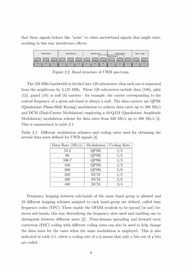
that these signals behave like “noise” to other narrowband signals that might exist,avoiding in this way interference effects.
Band Group 1 Band Group 4Band Group 6
Figure 2.2: Band structure of UWB spectrum.
The 528 MHz bandwidth is divided into 128 subcarriers, thus each one is separatedfrom the neighbours by 4.125 MHz. These 128 subcarriers include data (100), pilot(12), guard (10) or null (6) carriers - for example, the carrier corresponding to thecentral frequency of a given sub-band is always a null. The data carriers use QPSK(Quadrature Phase-Shift Keying) modulation to achieve data rates up to 200 Mb/sand DCM (Dual-Carrier Modulation) employing a 16-QAM (Quadrature AmplitudeModulation) modulation scheme for data rates from 320 Mb/s up to 480 Mb/s [4].This is summarized in table 2.1.
Table 2.1: Different modulation schemes and coding rates used for obtaining theseveral data rates defined for UWB signals [4].
Data Rate (Mb/s) Modulation Coding Rate53.3 QPSK 1/380 QPSK 1/2
106.7 QPSK 1/3160 QPSK 1/2200 QPSK 5/8320 DCM 1/2400 DCM 5/8480 DCM 3/4
Frequency hopping between sub-bands of the same band group is allowed and10 different hopping schemes assigned to each band group are defined, called timefrequency codes (TFC). These enable the OFDM symbols to be spread (or not) be-tween sub-bands, this way diversifying the frequency slots used and enabling one todistinguish between different users [2]. Time-domain spreading and forward errorcorrection (FEC) coding with different coding rates can also be used to help changethe data rates for the cases when the same modulation is employed. This is alsoindicated in table 2.1, where a coding rate of x/y means that only x bits out of y bitsare coded.
8

2.4 VCSEL2.4.1 Structure and Properties
VCSELs are a type of semiconductor laser diode in which the emitted light comesout perpendicular to its surface. The laser’s cavity is made using two Bragg mirrorsand the active medium is usually comprised of several quantum wells (figure 2.3),with a total thickness of just a few micrometers. This active region is electricallypumped by a ring electrode with typically a few tens of mW of power, generatingan output power from the laser up to 5 mW for single mode devices [15]. However,several other configurations for current injection and confinement within the activeregion are possible, each one presenting its own advantages and disadvantages tocommercial use [16].
Figure 2.3: General VCSEL structure, indicating the active region’s length (La) [2].
Giving the fact that this is a very small device it becomes fairly easy to obtainsingle frequency operation of the laser. However, due to these small dimensionsand due to the fact that it is harder to uniformly pump a larger active region, moretransverse modes can be excited if higher mode areas and, thus, higher output powersare desired, hence deteriorating the beam’s quality [15]. Also, VCSELs have low beamdivergence when compared to edge-emitting lasers and a symmetric beam profile,making it easy to collimate their output. Other important advantages of VCSELsinclude the very low threshold levels (µA level), the insensitivity of wavelengths totemperature variation, high-speed modulation capabilities (more than 10 Gb/s insome cases), long lifetimes (up to 107 hours in room-temperature operation) and
9

lower overall costs, arising from its vertical-cavity structure which gives the abilityfor testing each laser at intermediate stages of production and not just at the end[16].
Several wavelengths can be obtained using these devices, depending on the typeof semiconductor material that makes the active region and its surroundings. Thesewavelengths span a broad spectrum, from the long-wavelength band (1.3/1.55 µm),passing through the mid-wavelength band (0.98 µm) and the near-infrared band(0.78/0.85 µm) up to the green-blue UV band. For example: 1.3 µm or 1.55 µmwavelengths can be obtained with a GaInAsP-InP system with various types of mir-ror materials; 0.98 µm wavelengths can be obtained with a GaInAs-GaAs systemproviding threshold currents as low as a few hundreds of µA; and, GaAlAs-GaAssystems can be used for 0.85 µm wavelength emission [16].
2.4.2 Model
In order for the simulations of the transmitting system to be made a model of theVCSEL must be used so that its behavior can be correctly analyzed and predicted.This model is presented here, consisting of the rate equations and of the VCSEL’sequivalent electrical circuit, which includes the parasitic components caused by thelaser package and chip. This equivalent circuit is of extreme importance when dealingwith high frequencies because the frequency limits of the system will usually be definedby its parasitic components, therefore contributing to the response of the laser to theinput signal.
The rate equations for a VCSEL, which account for all processes that occur insidethe semiconductor material and that will affect the carrier (N) and photon density(P ), can be expressed as [2]
dN
dt= ηiI
qV− N
τ−RstP (2.1)
dP
dt= ΓRstP −
P
τp+NβΓRsp (2.2)
where ηi is the injection efficiency, V is the volume of the active region, I is theelectrical current, q is the value of the electron charge, τ is the carrier lifetime, Γ is aconfinement factor, Rst and Rsp are the stimulated and spontaneous emission rates,respectively, τp is the photon lifetime inside the cavity and β is the fraction of thetotal spontaneous emission coupled into the laser mode.
10

Equation 2.1 describes the rate of change of the carriers’ density N in the semicon-ductor. The first term accounts for the rate at which electrons or holes are injectedinto the active layer due to external pumping; the second term introduces the lossesof the carriers through spontaneous emission and non-radiative recombination; andthe last term accounts for those carriers that recombine through stimulated emissionand, therefore, contribute to the lasing process. In this last case the term can beapproximately written as [2]
RstP = vgg(N)P ≈ vga(N −N0m)(1− εP )P (2.3)
where vg is the laser’s group velocity, g(N) is the stimulated gain function, a = ∂g∂N
is the differential gain, N0m is the carrier density at zero gain and (1− εP ) is a phe-nomenological term describing gain compression, with ε being the gain compressionfactor with units of m3. The approximation for the stimulated gain function has beenmade by simply writing the initial logarithmic expression for g(N) in a Taylor series.
In equation 2.2, which describes the rate of change of the photons’ density insidethe cavity, the first term is due to the coherent photon generation through stimulatedemission, the second term accounts for the loss of photons from the cavity - with thephoton lifetime inside the cavity being given by 1
τp= vg
[αs + 1
Lln(
1R
)], and the last
term accounts for the rate of spontaneously generated photons. In this equation thefirst term can also be approximated by eq. 2.3, just like in the case of eq. 2.1 [2].
By measuring the frequency response of the laser at several bias currents, thefrequency subtraction method permits the extraction of the laser parameters, makingit possible to accurately simulate the behavior of a real device [17]. In this way, thestandard values that will be used were taken from [17, 18] and are given in table 2.2.
Table 2.2: Laser parameters used.
Parameter Value UnitV 2.4× 10⁻¹⁸ m3
g0 4.2× 10⁻¹² m3s−1
ε 2.0× 10⁻²³ m3
N0m 1.9× 1024 m−3
β 1.7× 10⁻⁴ -Γ 4.5× 10⁻² -τP 1.8 psτS 2.6 nsηi 0.8 -Ith 0.893 mA
11

As far as the VCSEL’s equivalent electrical circuit is concerned, figure 2.4 repre-sents the model used - a RLC resonant [2] circuit acting as a low-pass filter with acutoff frequency of 7.4 GHz (measured with ADS™). It is comprised of an inductorLP , a capacitor CP and a resistor RS (the so-called parasitic components) in serieswith the active region (intrinsic laser diode (ILD)) described by the aforementionedrate equations. Above threshold this ILD can be electrically viewed as a short-circuitat all frequencies when comparing to other relatively large components’ impedanceswhich make up the circuit model [2]. These values of the components were takenfrom [19] and are given in table 2.3.
ActiveRegion
IS
LP
CP
RS
Ia
Rin
Zeq
Figure 2.4: VCSEL equivalent circuit of the laser parasitics.
Table 2.3: Values of the parasitic components.
Component Value UnitRS 76 ΩCP 0.39 pFLP 2.28 nH
The components LP and CP are due to the laser package and represent the wire-bond inductance and the contacts capacitance, respectively. The series resistor RS
represents the contacts resistance as well as the Bragg mirror stacks [2] (DistributedBragg Reflectors (DBR) elements in figure 2.3).
The frequency behavior of this equivalent circuit model (assuming that the ILDis a short-circuit, as already explained) can be described by means of its equivalentimpedance Zeq, given by
Zeq = RS
1 +R2SC
2Pω
2 + j
(ωLP −
ωR2SCP
1 +R2SC
2Pω
2
)(2.4)
2.4.3 Small Signal VCSEL Response
The VCSEL rate equations can be linearized if one considers the small signal responseof the laser. In these conditions, the transfer function of the laser can be found for
12

different bias currents. An example is given in figure 2.5, where the magnitude ofthe first-order transfer function H(f) (defined as the ratio of the photon density to aperturbed current) is presented for 3 mA and 6 mA bias currents. This transfer func-tion represents the frequency response of both the laser and its equivalent electricalcircuit discussed in the previous subsection.
0 5 10 15−35
−30
−25
−20
−15
−10
−5
0
5
10
15
Frequency (GHz)
Am
plitu
de |
H(f
) | (
dB)
3 mA
6 mA
Figure 2.5: Small signal transfer function of the VCSEL.
It can be seen that for the highest bias current the peak has a lower value and is ata higher frequency than the 3 mA peak, this way increasing the available modulationbandwidth and flattening the overall behavior. Without considering other effects inthe laser, this is expected to continue to happen with increasing currents until thelimit is reached [20].
2.4.4 Relative Intensity Noise
In all kinds of lasers, and VCSELs in particular, noise is an intrinsic random pro-cess which plays an important role in defining the quality of the output laser beam.This beam, in the case of lasers which are used in optical communication systems,is responsible for the transmission of data. Therefore, its quality is of extreme im-portance because it will be related to the definition of several important propertiesof the system, such as its maximum range and bit error rate (BER). In VCSELs andother types of semiconductor laser diodes, the noise can be generated by spontaneousemission of photons or by carrier generation or recombination processes.
It is clear that an understanding of the noise generated in these kind of devices isimportant to correctly model their behavior and to adequately simulate the transmit-ting system. Although a complete description of noise in semiconductor laser diodes
13

relies on a quantum formulation of the rate equations, a semiclassical approach usuallysuffices in describing its behavior.
In this way, the time-dependent optical power emitted from a VCSEL can bedescribed in the following way
P (t) = 〈P (t)〉+ δP (t) (2.5)
where 〈P (t)〉 = P0 is the steady-state photon density and δP (t) represents the noiseadded to the signal. The intensity noise at a given frequency can be characterized bythe relative intensity noise (RIN) [2]
RIN = Sp(ω)P 2
0(2.6)
where Sp(ω) is the power spectral density of the random process δP (t) given by theWiener–Khinchine theorem
Sp(ω) =∫ ∞−∞〈δP (t+ τ)δP (t)〉 e−iωτdτ (2.7)
Usually the RIN is defined in dB/Hz. Re-writing eq. 2.6 to explicitly show thedependence on the signal bandwidth ∆f and to obtain the value in dB, we get [21]
RIN = 10 log10
(〈δP (t)2〉P 2
0 ∆f
)(2.8)
where 〈δP (t)2〉 represents an averaged value of the square of the noise total power.From here, and considering a photodetector with a given responsivity r = I
P, it is
fairly straightforward to obtain the noise current as a function of the signal’s opticalpower ⟨
I2⟩RIN
= P 20 r
210RIN10 ∆f (2.9)
The RIN spectrum does not present a constant behavior because it has a specificpeak at a given resonance frequency for a single mode device and several peaks formulti-mode ones [21]. However, below and above these frequencies the RIN spectrumis considerably flat and in the simulations it will be assumed that the VCSEL isoperating in these regions.
2.5 SummaryThis chapter presented the main features of a technology which merges optical andwireless networks, the Radio-over-Fiber technology. This technology allows for better
14

coverage for services which need high data-rates by using the best properties of bothworlds, like the low losses and high bandwidths of fiber optics and the mobility ofRF wireless links. It is a technology which can present lower costs and can be usedindoors as well as outdoors, by replacing other wired systems. It is clear that itpresents several advantages over other competing communication systems (which usecoaxial lines or are based only on wireless networks) for some applications and its useis, therefore, expected to increase in the next years.
More details of UWB signals have also been given, namely the fact that they useeither QPSK or DCM modulations depending on the data rates desired and thatthese signals are generated using OFDM techniques. Some of the codes these signalsuse for varying the data rates and distinguishing between users, like TFC and FECcodes, respectively, have also been presented.
The other topic focused during this chapter was the VCSEL. It was explained thatit can be made of several cascaded quantum wells and that its particular structureprovides properties to the laser beam which can be very appreciated in some ap-plications, such as an easier to obtain monochromaticity, good beam symmetry andlower costs when compared to edge-emitting diode lasers. Moreover, the VCSEL’srate equations were detailed and its equivalent electrical circuit model was presented,noting that it acts as a low-pass filter with cutoff frequency of 7.4 GHz. These allowone to be able to reliably predict the VCSEL’s dynamic behavior in the simulations.Another aspect covered concerns a very important type of noise occurring in diodelasers - the RIN. This noise is always present, having a peaked spectrum with flatbehavior far from the resonance frequencies. A description of the RIN is needed inorder to make the simulations even more reliable.
15
Chapter 3
Design of RF Amplifiers
3.1 IntroductionThis chapter deals with the main techniques used to design the LNA needed for thetransmitter, whether that be with discrete commercial off-the-shelf (COTS) compo-nents or by using a MOS process. Each technology to be used presents features thatmake these techniques different, so they must be detailed separately.
The following section will introduce some of the techniques that have been usedto design the discrete version of the LNA. These will allow one to obtain the desiredfeatures when designing the actual device later on and to assess its properties like,for example, the stability conditions, the gain and the whole ensemble noise.
The techniques for designing an analogue microelectronics amplifier for integratingthe transmitter using a MOS process are detailed afterwards. In this section, the mainconcerns and differences from the design of the discrete version are also explained,justifying the need to consider some new effects while neglecting others.
This chapter is finalized with a brief summary of the main conclusions.
3.2 Techniques for Designing Discrete RF Ampli-fiers
One of the most important components of our transmitter is the LNA, which will beused to amplify an input signal before it can be fed into the VCSEL and transmittedover an optical fiber. The PCB version of this amplifier should then be designedcarefully, using transmission line theory due to the high operating frequencies andrelatively large dimensions, as any problem it possesses can significantly affect theinformation to be transmitted.
16

In order for an amplifier to behave properly and not oscillate when an input signalis applied, its frequency stability should be verified. This verification can be madeusing the K −∆ test based on the transistor’s scattering-parameters (S-parameters)[22]:
K = 1− |S11|2 − |S22|2 + |∆|2
2 |S21S12|> 1 (3.1)
|∆| = |S11S22 − S21S12| < 1 (3.2)
where K is called the stability factor.The S-parameters are specific to an electrical system or network and they relate
the reflected voltages with the incident ones. For example, for a two-port network(figure 3.1), the S-parameters’ matrix is defined as [22]:
(V −1V −2
)=(S11 S12S21 S22
)(V +
1V +
2
)(3.3)
where V −1 /V −2 are the reflected voltages at port 1/port 2 and V +1 /V
+2 are the incident
voltages.
[S]
Port 1 Port 2
V1 V2
+
-
+
-
I1 I2
Figure 3.1: Schematic diagram of a 2-port network.
If the K−∆ test conditions are not satisfied that means the amplifier is condition-ally stable (or potentially unstable). In this case, the stability circles for the sourceand the load must be obtained in order to find the appropriate matching conditionsbetween the source and the load and the amplifier itself, in order to guarantee a stablebehavior.
After the stability of an amplifier is assessed, one should start thinking on howto obtain the desired gain. Figure 3.2 represents a diagram of an amplifier, whichincludes a transistor, supposed to be described by the S-parameters, and the cor-responding matching circuits at the input and output. The overall transducer gainof an amplifier is basically dependent on its intrinsic power gain (G0, given by thetransistor’s |S21|2) and on the impedance matching sections used, as can be seen fromthe next relation [22]
17
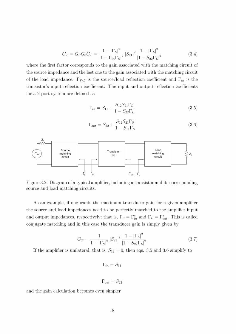
GT = GSG0GL = 1− |ΓS|2
|1− ΓinΓS|2|S21|2
1− |ΓL|2
|1− S22ΓL|2(3.4)
where the first factor corresponds to the gain associated with the matching circuit ofthe source impedance and the last one to the gain associated with the matching circuitof the load impedance. ΓS/L is the source/load reflection coefficient and Γin is thetransistor’s input reflection coefficient. The input and output reflection coefficientsfor a 2-port system are defined as
Γin = S11 + S12S21ΓL1− S22ΓL
(3.5)
Γout = S22 + S12S21ΓS1− S11ΓS
(3.6)
Sourcematching
circuit
Transistor[S]
Loadmatching
circuit
Z0
Z0
ΓS ΓL Γin Γout
Figure 3.2: Diagram of a typical amplifier, including a transistor and its correspondingsource and load matching circuits.
As an example, if one wants the maximum transducer gain for a given amplifierthe source and load impedances need to be perfectly matched to the amplifier inputand output impedances, respectively; that is, ΓS = Γ∗in and ΓL = Γ∗out. This is calledconjugate matching and in this case the transducer gain is simply given by
GT = 11− |ΓS|2
|S21|21− |ΓL|2
|1− S22ΓL|2(3.7)
If the amplifier is unilateral, that is, S12 = 0, then eqs. 3.5 and 3.6 simplify to
Γin = S11
Γout = S22
and the gain calculation becomes even simpler
18
GTU = 11− |S11|2
|S21|21
1− |S22|2(3.8)
It should be noted that this gain is not exactly correct if a S12 parameter exists,which in reality it does even if it is quite small. But in these cases the differencebetween the unilateral gain and the real gain is also small, so if the S12 parameteris indeed insignificant the unilateral gain equation is used in order to simplify calcu-lations and to provide a gain estimate for future circuit optimization. By using theunilateral figure of merit, U , defined as
U = |S11| |S22| |S21| |S12|(1− |S11|2
) (1− |S22|2
) (3.9)
the error made by this simplification can be bounded in the following way
1(1 + U)2 <
GT
GTU
<1
(1− U)2 (3.10)
Usually, a maximum value of U = 0.1 is desired for the unilateral approach to beconsidered acceptable, because it brings an error of less than ±1 dB [23].
Impedance matching can be achieved in several ways, but since this is a RF cir-cuit one should not use lumped elements but transmission lines instead, as alreadydiscussed. One of the main techniques for impedance matching uses stubs, that is,transmission lines in short or open-circuit placed at a specific distance from the un-matched impedance using a connecting line, as represented in figure 3.3. In this way,the input impedance of the circuit is controlled by the parameters of the transmissionlines. It should be noted that for microstrip lines (figure 3.4), which are the type oflines that will be used, open-circuits are usually preferred due to simplicity of fabri-cation. It should also be noted that an unconditionally stable amplifier can alwaysbe designed for maximum gain, since it can present any desired reflection coefficientfor a stable behavior.
19

YL
L
d
Y0
Y0
Y0
Y=1/Z
Figure 3.3: Matching circuit using stubs: L is the length of the stub and d is itslength position along the transmission line.
Figure 3.4: Microstrip line model: d is the thickness of the substrate with εr permit-tivity and W is the width of the line [3].
However, if a specific gain is given that does not correspond to the maximumpossible one, then an impedance mismatch needs to be intentionally created so thatthe amplifier’s total gain matches the one desired. The amount of mismatch can befound from eq. 3.4, by simply obtaining the reflection coefficients ΓS and ΓL. Then,it is just a matter of obtaining the necessary stub parameters with a Smith Chart toget an amplifier with the desired gain [22].
As far as the noise figure of the amplifier is concerned - a parameter of greatimportance in low noise systems - it can be computed using the Friis formula, anexpression suitable for receiving systems comprised of cascaded components whichpresent gain and noise generation and usually defined as [3]
FT = F1 + F2 − 1G1
+ F3 − 1G1G2
+ ... (3.11)
where F1 represents the noise figure of the receiver’s first component and G1 its gain,and so on to as many components as the cascaded system presents.
For the specific case of a single transistor, its noise figure can be determined using[22]
F = Fmin +4RN
50|ΓS − Γopt|2(
1− |ΓS|2)|1 + Γopt|2
(3.12)
20
where RN50
is the transistor’s equivalent noise resistance referenced to 50 W, Γopt isthe source reflection coefficient which determines the minimum noise and Fmin is theminimum noise figure (when ΓS = Γopt).
3.3 Integration Using a MOS ProcessTo design the integrated version of our transmitter one must account for some issuesthat were not addressed during the design of the discrete version and that are nowof extreme importance. Such issues are related to the size and non-idealities of thecomponents placed in the circuit and their layout, which will certainly influence theIC’s performance. Common non-idealities include intrinsic parasitic effects in thecomponents (like the transistors, bondpads and bonding wires) which arise from theirphysical implementation and which can be minimized through, for example, sizereduction. Thus, the correct design and layout of the components that make thistransmitter will allow one to reduce the total intrinsic effects. Nevertheless, they willalways exist and, therefore, need to be considered in the simulations.
Since the layout of the integrated circuit is one of the main goals of this work, itshould be noted that its creation is governed by some rules to ensure its appropriateoperation when considering the presence of the aforementioned component - and evenproduction materials - non-idealities. These rules are related not only to the transistorlayout, but also to all other elements which make the integrable circuit.
3.3.1 Analogue Microelectronics Theory
Some of the theory for assessing a RF circuit’s properties has already been addressedin section 3.2, as they are essentially the same whether we are considering a PCB oran IC.
However, the design of an analogue microelectronics circuit is very different fromthe design of a circuit based on discrete components. In this case, since one needsto design the transistors themselves, their models need to be studied and their di-mensions need to be correctly found because the system’s properties may vary con-siderably with them - for example, a bigger transistor can provide higher gain but itwill also have larger intrinsic components (mainly capacitances between its terminals)which will worsen the behavior at higher frequencies.
In this way, the small-signal equivalent circuit model of a field-effect transistor(FET) is represented in figure 3.5, showing a grounded source terminal and including
21

the effect of channel-length modulation through the resistance ro [24], as well as someintrinsic elements (such as the capacitances CGS and CGD).
G D
S
gmvGS roCGS
CGD
Figure 3.5: Small-signal equivalent circuit model of a FET when considering thechannel-length modulation effect and some intrinsic capacitances.
The transistor’s physical dimensions when neglecting channel-length modulationcan be found using the following expression[25]
W
L= gmµCoxVGSef
(3.13)
where W is the transistor’s width and L its length, gm = 2IDS
VGSefis the transconduc-
tance, µCox is the transistor’s intrinsic transconductance and VGSef = (VGS − VT ) isthe effective gate-to-source voltage.
It is the transconductance of a transistor together with its output resistance (Rout,which is dependent on the load of the transistor) which determines the gain, as givenby the following expression
A = gmRout (3.14)
However, the achievement of this gain is dependent not only on the transistoritself but also on external factors, such as impedance matching. Impedance matchingcan be achieved in more than one way, but in this case it will be used the scheme offigure 3.6 for input matching. It should be noted that since IC connections inherentlypresent lower physical dimensions than a common PCB’s, their design is made withoutconsidering transmission lines nor their consequent circuit design implications, suchas in impedance matching - hence the lumped elements used in the matching scheme.This is because the lowest operating signal wavelength is approximately 8 cm, a verylarge value compared to typical IC lines’ dimensions.
22

CpadLbonding
Z
LGCG
Zin
ZL
Figure 3.6: Input impedance matching scheme used.
In figure 3.6, an inductance (LG) is used in series with the capacitance used forDC-coupling (CG) to match the input impedance of the transistor to the source’simpedance. This input impedance is given by [25]
Zin = −j 1ωCGS
+ Z + gmZ
jωCGS(3.15)
where Z is the bondpad and bonding wire equivalent impedance (refer to figure 3.7for their equivalent model), which usually becomes Z ≈ jωLbonding for small valuesof bondpad capacitance (Cpad). This model for the transistor’s input impedance doesnot take into account the gate resistance, the gate-to-drain capacitance (CGD, whoseinput effect can become very large due to the Miller effect), the output resistance orother intrinsic components and, therefore, it will be used just as a guiding model forlater tuning.
Pin Frame
CircuitLbonding
Cpad
Figure 3.7: Bondpad and bonding wire model.
As can be seen this input impedance is mainly capacitive, but it also presents areal part. If one wants to match this impedance to a 50 W source the imaginary partwould need to be zero and the real part 50 W, yielding the following conditions for
23
the components [25]
f0 = 1
2π√
(Lbonding + LG)(CGSCG
CGS+CG
) (3.16)
gmLbondingCGS
= 50 (3.17)
The output matching can be considerably simpler since the channel resistancero is considered infinite (no channel-length modulation effect), making the outputimpedance only dependent on the bondpad and bonding wire equivalent impedance(typically very small), on the CGD capacitance referred to the output (Miller effect)and on the output DC-coupled capacitor (Cout). Hence, the output impedance isfound to be solely capacitive, but in reality this is not completely true because a realpart is always present. Nevertheless, the DC-coupled capacitor Cout can be used toobtain good matching because its value can be (almost) freely changed.
3.4 SummaryIn this chapter, some of the techniques that are needed to assess the properties ofthe discrete LNA and to obtain the desired features in the implementation stage werepresented, including how impedance matching should be made to obtain the neededreflection coefficients.
Then, the basic theory for designing analogue microelectronic circuits was pre-sented, in order to enable the integration of the transmitter using a MOS process. Inthis section, several design constraints that appear only when using these technologieswere explained so that they can be considered in the circuit design and simulation.For example, the fact that IC design implies small connection dimensions means thatimpedance matching is not necessary between components inside the chip and thatlumped elements can be used for input and output impedance matching.
24

Chapter 4
Design of the Optical Transmitterfor a 3.168-3.696 GHz UWB Signal
4.1 IntroductionThis chapter deals with the design of the optical transmitter for UWB signals inthe 3.168-3.696 GHz frequency range, which is basically comprised of a RF low-noiseamplifier (LNA) plus the VCSEL and its biasing circuit. Specifically, one wants todesign a LNA for the 4 GHz limit to allow for the amplification of the signals in thedesired frequency band, before they can be fed into the VCSEL for electrical-to-opticalconversion and consequent fiber transmission. This LNA, in its discrete version, iscomprised of two cascaded single-voltage enhanced-mode pHEMT (pseudomorphicHigh Electron Mobility Transistor) transistors from Avago Technologies, designed formaximum gain. In the integrated version, the LNA will also be made of two transistorsdesigned using a specific process. To complete the description of the transmitter, thenext section will present its general structure.
Then, the techniques presented in the previous chapter are applied to specifi-cally calculate the main properties of the discrete LNA, like its frequency stability,maximum unilateral gain and noise figure.
After that, the biasing networks used to correctly bias both transistors and theVCSEL are presented, indicating the components used and showing how they wereobtained to provide for proper transistor or VCSEL operation, without ignoring theireffects on the whole transmitter.
Then, the steps taken towards obtaining the desired source and load reflectioncoefficients for getting the maximum gain are presented by explaining the impedancematching circuits designed for the discrete LNA.
25

The following section presents the MOS process used in the integration of thetransmitter, as well as its main features.
The integration of this device using a MOS process with the microelectronicstheory previously presented is detailed afterwards, providing some of the specificcharacteristics of this circuit and its components, like the transistor’s dimensions andgain.
This chapter is finalized with a brief summary of the main results and conclusionspresented herein.
4.2 General Structure of the TransmitterThe transmitter to be designed presents a simple structure: three matching networkswhich allow for impedance matching between components of the device, two tran-sistors which provide amplification and their biasing circuit, a VCSEL for electrical-to-optical conversion and also its biasing circuit. A block diagram representing thisstructure is depicted in figure 4.1, which is the same no matter which design versionis being considered.
UWB
Source
Matching
Network 1Transistor 1
Matching
Network 2Transistor 2
Matching
Network 3VCSEL
Biasing
Circuit
Biasing
Circuit
Figure 4.1: General scheme of the transmitter to be designed.
A detailed explanation of the design of the electrical components which make thisdevice is given in the following sections.
4.3 Properties of the Amplifier4.3.1 Frequency Stability
By utilizing the K − ∆ test discussed in section 3.2, this key parameter for everyamplifier has been assessed, with eqs. 3.1 and 3.2 yielding the following results
K = 0.896 < 1
26

|∆| = 0.268 < 1
for the following transistor S-parameters (at 4 GHz) [26]
S11 = 0.513∠175.4º
S21 = 5.13∠49.1º
S12 = 0.075∠14.2º
S22 = 0.345∠− 74.3º
These results show that the LNA is conditionally stable at the chosen designfrequency (4 GHz). As previously stated, the stability circles need to be found inorder to design the amplifier’s matching circuits using stable reflection coefficients.The source and load stability circles for each transistor obtained with ADS™ arepictured in figure 4.2, as well as the reflection coefficients ΓS = S∗11 and ΓL = S∗22
represented by the red dots in each circle, which provide maximum unilateral gain.Moreover, since |S11| < 1, the center of the Smith chart (ΓS/L = 0) belongs to a stableregion.
(a) Source stability circle and ΓS . (b) Load stability circle and ΓL.
Figure 4.2: Stability circles for the amplifier at 4 GHz with the used reflection coef-ficients.
27
It can be clearly seen from the figure that for these values of ΓS = S∗11 andΓL = S∗22 the amplifier is stable and with enough distance from the unstable regionto allow for some stability margin. Hence, despite this amplifier being potentiallyunstable at 4 GHz, it was still possible to design it with a gain equal to the maximumunilateral gain. Furthermore, it has been confirmed that, despite this amplifier beingalso potentially unstable throughout the entire signal frequency band, the choice ofΓS = S∗11 and ΓL = S∗22 still provides a stable behavior at all these frequencies.
4.3.2 Gain
The gain of the LNA is given by the gain of each of its composing transistor’s anddepends on the matching obtained with the impedance matching networks, as alreadyexplained in section 3.2. With the reflection coefficient values given in the previoussubsection we can easily calculate the unilateral gain of each transistor and of thewhole amplifier.
In this way, by using eq. 3.7 and the corresponding reflection coefficients, themaximum gain for each transistor is
GMax = 1.34 dB + 14.2 dB + 1.14 dB = 16.1 dB
and, hence, the ensemble’s total gain is simply
GLNA = 2×GMax = 32.2 dB
Since this is the unilateral gain the error to the actual gain can be estimated.The unilateral figure of merit for each transistor is obtained using eq. 3.9 and thecomponent’s S-parameters, giving
U = 0.10
which is the maximum allowed value for considering a unilateral approach. From eq.3.10, where GMax = GTU , this bounds the error in the following way
0.83 < GT
GTU
< 1.23
and, in dB,
−0.81 dB < GT −GTU < 0.89 dB
From these values we can conclude that the unilateral assumption gives a trans-ducer gain with an error within 1.7 dB. However, should the U parameter be a little
28
higher, the amplifier would need to be designed considering the more realistic bilateralbehavior so that a higher error could be avoided.
4.3.3 Noise Figure
By replacing the constants in eq. 3.12 with the ones specific of the chosen transistors[26] (available only at a frequency of 3.9 GHz) and by using ΓS = S∗11 as previouslydiscussed, the noise figure for each transistor is obtained, giving
F = 0.98 dB
With these noise figures and with the gain value determined in the previous sec-tion, we can compute the LNA’s noise figure by making F1 = F2 = 1.25 (0.98 dB)and G1 = 40.7 (16.1 dB) in eq. 3.11, giving
FLNA = 1 dB
It is expected that the noise figure be lower at the operating frequencies, sincethis value was obtained for a higher frequency.
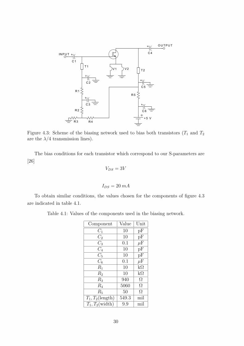
4.4 Transistors’ Biasing Network DesignThe two transistors used in this transmitter need to be correctly biased in order toensure its appropriate operation. In this case a single circuit will be used to bias bothtransistors to simplify the final overall circuit.
The circuit used for this purpose is represented in figure 4.3. This circuit is basedon the one provided in the transistor’s datasheet [26] and it is a passive type of biasingnetwork comprised of a 5 V source, several resistors, capacitors and high impedanceλ/4 transmission lines (components T1 and T2 in the figure). The resistors contributeto current limitation, voltage division and improved low frequency stability; the C1
and C4 capacitors provide the DC-coupling; and the other capacitors and the λ/4transmission lines provide the required isolation between the signal and biasing net-works. The high impedance λ/4 transmission lines are used instead of inductors toprovide for better performance at high operating frequencies.
29
+ 5 V
C 1
C 2
C 3
R 1
R 2
R 3 R 4
R 5
C 4
C 5
C 6
V 2V 1T1
T2
IN P U T
O U TP U T
Figure 4.3: Scheme of the biasing network used to bias both transistors (T1 and T2are the λ/4 transmission lines).
The bias conditions for each transistor which correspond to our S-parameters are[26]
VDS = 3V
IDS = 20mA
To obtain similar conditions, the values chosen for the components of figure 4.3are indicated in table 4.1.
Table 4.1: Values of the components used in the biasing network.
Component Value UnitC1 10 pFC2 10 pFC3 0.1 µFC4 10 pFC5 10 pFC6 0.1 µFR1 10 kΩR2 10 kΩR3 940 ΩR4 5060 ΩR5 50 Ω
T1, T2(length) 549.3 milT1, T2(width) 9.9 mil
30

Some of these values are given in [26], like for the components C3, C6, R1 andR2, but others were calculated using simple DC circuit analysis. Such is the case ofresistors R3, R4 and R5, whose values were obtained using [26]
R3 = VGSIBB
(4.1)
R4 = (VDS − VGS)R3
VGS(4.2)
R5 = VDC − VDSIDS + IBB
(4.3)
where VGS = 0.47 V , IBB = 0.5mA and VDC = 5 V . It should be noted that, in thiscase, IDS = 40 mA because a single circuit will bias both transistors, so one had todesign it for delivering twice the current necessary for each one.
The λ/4 transmission lines’ physical dimensions were obtained (in mils1) usingthe LineCalc tool from ADS™ and considering an operating frequency of 3.432 GHz(UWB signal’s central frequency), 90º of electrical length and an impedance whichcorresponds to approximately 99 W.
The values for the rest of the components - namely the capacitors C1, C2, C4
and C5 - were obtained by tuning, utilizing the lowest possible values that did notcompromise the system’s performance.
V1 and V2 components represent simple vias which connect the top side of thesubstrate to its bottom side.
4.5 VCSEL Biasing Network DesignThe VCSEL also needs a biasing circuit in order to correctly set its working point.This biasing circuit will not only allow for the diode laser to work above the thresholdcurrent, it will also be responsible for setting the RIN current (as seen in eq. 2.9), thuscontributing to its overall performance. Therefore, the DC current value which will beinjected by this biasing network needs to be carefully chosen in order to obtain goodresults - in this case, a bias current of Ib = 6 mA has been found to be a sufficientlygood bias point.
The bias network used to deliver this current in represented in figure 4.4, whichalso indicates its relative position in the transmitter. This bias network is comprisedof a 5 V power source, a resistor Rb for setting up the DC current, an inductor Lb
1mil = thousandth of an inch or 2.54× 10⁻⁵ m
31

for preventing the leakage of the UWB signals through this circuit and a capacitorCb for DC-coupling.
+5 V
Rb
Lb
Cb
VCSELLoad
MatchingCircuit
Figure 4.4: Biasing network for the VCSEL.
The values of the components are indicated in table 4.2. The value for the resistorRb has been obtained by simply using the Ohm’s Law (Vb = 5 V ), with the totalresistance being the sum of Rb with RS = 76 Ω (subsection 2.4.2), this way ensuringthat the current which is really being fed into the ILD is 6 mA,
Rb = VbIb−RS (4.4)
Table 4.2: Values of the components of the VCSEL biasing network.
Component Value UnitRb 757 ΩLb 40 nHCb 10 pF
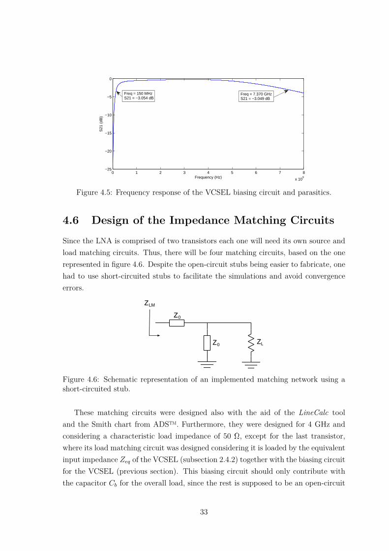
The values of the components Cb and Lb have been obtained by tuning since theirpurpose is filtering, but guaranteeing that the LNA is not significantly affected fromthe desired behavior, that is, guaranteeing they only filter the DC and the signalcomponents, respectively. The effects of these electrical components together withthe ones which compose the electrical circuit model for the VCSEL (see subsection2.4.2) are depicted in figure 4.5, as well as the cutoff frequencies. It can be seen thatthe attenuation at the operating frequencies is negligible.
32
0 1 2 3 4 5 6 7 8
x 109
−25
−20
−15
−10
−5
0
Frequency (Hz)
S21
(dB
)
Freq = 7.370 GHzS21 = −3.049 dB
Freq = 150 MHzS21 = −3.054 dB
Figure 4.5: Frequency response of the VCSEL biasing circuit and parasitics.
4.6 Design of the Impedance Matching CircuitsSince the LNA is comprised of two transistors each one will need its own source andload matching circuits. Thus, there will be four matching circuits, based on the onerepresented in figure 4.6. Despite the open-circuit stubs being easier to fabricate, onehad to use short-circuited stubs to facilitate the simulations and avoid convergenceerrors.
Z0
Z0
ZLM
ZL
Figure 4.6: Schematic representation of an implemented matching network using ashort-circuited stub.
These matching circuits were designed also with the aid of the LineCalc tooland the Smith chart from ADS™. Furthermore, they were designed for 4 GHz andconsidering a characteristic load impedance of 50 W, except for the last transistor,where its load matching circuit was designed considering it is loaded by the equivalentinput impedance Zeq of the VCSEL (subsection 2.4.2) together with the biasing circuitfor the VCSEL (previous section). This biasing circuit should only contribute withthe capacitor Cb for the overall load, since the rest is supposed to be an open-circuit
33

for the signals. The final result for the load impedance of the second transistor isthen Zmatch:
Zmatch = Zeq −j
ωCb
= RS
1 +R2SC
2Pω
2 + j
(ωLP −
1ωCb
− ωR2SCP
1 +R2SC
2Pω
2
)(4.5)
which becomes Zmatch = 48.9 + j16.8 at 4 GHz.The ZLM impedance represented in the figure is the required matched load impedance,
that is, it is the value of the impedance one wishes to obtain after introducing thematching networks. It corresponds to the desired value of the reflection coefficient,using the following expression
ZLM = Z0 + ΓZ0
1− Γ (4.6)
where Z0 = 50 Ω and Γ = ΓS/L which, in this case, corresponds to Γ = S∗11 or Γ = S∗22
for maximum unilateral gain.After all of the transmission lines’ dimensions were obtained, a simplification has
been performed. This simplification is schematically explained in figure 4.7, where theload matching network of the first transistor and the source matching network of thesecond transistor were simplified by summing the admitances of the short-circuitedstubs, so that only one short-circuited stub is used.
Transistor
1
Transistor
2
Transistor
1
Transistor
2
Figure 4.7: Simplification made to the matching networks between the first and thesecond transistor.
Moreover, some fine tuning has been made to two of the lines in these matchingnetworks to attain a better frequency response. The final result, however, was notmuch different from the original, whether that be in the case of the lines’ dimensions(given in table 4.3) or in the case of the final frequency response of the LNA.
34

Table 4.3: Dimensions of the transmission lines (TL) and stubs (S) used in thematching networks 1, 2 and 3 of figure 4.1. For example, the length of the first lineof the matching network 2, TL2,1, is 143.5 mil.
Component Value UnitLength
TL1 134.5 milS1 694.7 mil
TL2,1 143.5 milS2 576.5 mil
TL2,2 134.5 milTL3 71.7 milS3 370.6 mil
WidthAll 43.2 mil
4.7 MOS ProcessThe MOS process to be used in the integration is an IBM 130 nm. The choice of thisprocess was based on its proposed characteristics, like the material’s response times,which is of absolute importance when considering a device that needs to work in thegigahertz range. These response times allow for a transition frequency that is abovethe frequency range the transistor is supposed to operate on. Other advantages ofthis process when compared to others that use different feature sizes is the fact that,with this one, one can produce a transmitter with smaller components and, hence,with lower power consumption and smaller intrinsic effects.
This process allows the use of five to eight different metal levels with differentthicknesses. The metallization is made with copper or aluminum, depending on thelevel being considered – for example, the last level is usually made with copper.Isolation between devices is achieved with a shallow trench [27], which is a featurethat creates trench patterns in the silicon and then fills them up with one or moredielectric layers, this way minimizing leakage currents.
4.8 Design of the IC TransmitterAs already explained in the previous chapter, every transmission line which has beenused in the discrete version no longer exists because there are no propagation effects.This means that the λ/4 transmission lines in the biasing networks were replaced byinductors. Also, impedance matching is no longer achieved using transmission lines
35

but with lumped elements, as already discussed. The inductors were considered topresent a quality factor (Q factor) whose chosen value differs whether they are insidethe IC itself (Q = 5) or outside of it (Q = 50).
The first topic addressed was designing two transistors for the desired gain, thatis, the same as the discrete version if possible. Starting from the signal currentamplitude desired to feed the VCSEL - which is 1.2 mA considering the outputresistance “seen” by the last transistor - the IDS current could be defined, this waymaking it possible to calculate the corresponding transistor’s transconductance, gainand physical dimensions by using the expressions presented in the previous subsection.The dimensions were found by also taking into consideration the transition frequency(FT ) of the transistor. The real biasing conditions for this transistor were simulatedand found to be VGSef = 70 mV and IDS = 3.9 mA, implying a transconductanceof gm = 0.11 A
V. The first transistor has the same size and also presents the same
biasing conditions as the last one. Furthermore, it has been found that both of them,besides having the same dimensions (W = 118 µm and L = 130 nm), also presentsimilar gains. As an example, the power gain of the last transistor was estimated tobe around 17 dB.
As far as the biasing network is concerned, the same kind of circuit as representedin figure 4.3 is used, once again employing one for both transistors in order to minimizecomplexity. Also, some of its components, namely the resistors R3, R4 and R5, havebeen altered to attend to the fact that the highest power supply voltage allowed forthis technology is 3.3 V [27] and also for meeting the new biasing specifications. Thevalues of the components used are indicated in table 4.4.
Table 4.4: Values of the components of the IC biasing network.
Component Value UnitC2 10 pFC3 0.1 µFC5 10 pFC6 0.1 µFR1 10 kΩR2 10 kΩR3 910 ΩR4 5090 ΩR5 60 Ω
The VCSEL biasing network is also the same as before (providing the same 6 mAbias current), but once again the values of its components are different due to the
36
change in the power supply voltage and due to the fact that this circuit will also affectthe output impedance of the last transistor, this way changing its gain conditions.The new values of the components of the VCSEL biasing network are presented intable 4.5.
Table 4.5: Values of the electrical components used for the VCSEL biasing networkin the IC.
Component Value UnitRb 474 ΩLb 20 nH
As already mentioned, the bondpads and bonding wires existent in every IC mayalso alter its behavior, making it necessary to consider them in the simulations forbetter assessing the final device behavior. Their simple electrical model has alreadybeen presented in figure 3.7: it is comprised of a parallel capacitor (representingthe pad) and a series inductor (representing the bonding wire). The bonding wire’sinductance (Lbonding) was considered to be 1 nH and the bondpad’s capacitance (Cpad)was found to be 17 fF for a 73 mm x 73 mm pad [28].
Impedance matching to a 50 W source at the input and to the VCSEL equivalentimpedance at the output of the circuit was made according to the models detailedin subsection 3.3.1, but as already said these models do not take into account manyimportant elements which affect the input impedance (even the inductors of the bias-ing networks considerably affect it). This way, tuning has been made to the values ofthe components given by the models in order to obtain an acceptable matching, butthe overall scheme presented in figure 3.6 has been maintained. The VCSEL modelconsidered for the output impedance matching is the same as presented in subsection2.4.2.
4.9 SummaryIn this chapter the techniques for designing RF amplifiers have been put to use,allowing one to obtain the desired devices and to assess their properties.
Specifically for the discrete version of the transmitter, one has found that its LNAis potentially unstable at the operating frequencies, although being still possible toobtain maximum unilateral gain from it by designing the matching circuits to haveΓS = S∗11 and ΓL = S∗22. This gain has been found to be 16.1 dB for each transistorand, therefore, 32.2 dB for the system of two cascaded transistors which make the
37
LNA. With this gain being calculated assuming that it presents a unilateral behavior,the error to the actual obtainable gain has been estimated to be within 1.7 dB. Also,the noise figure for the whole ensemble was found to be 0.98 dB, a low value asdesired.
Both biasing networks needed for the transmitter have been presented. Theseinclude the biasing network for both transistors, yielding voltages and currents inthe transistors close to VDS = 3V and IDS = 20 mA for them to work properly, andalso having components which serve as filters and impedance matching networks todeliver some desirable features. The other biasing network detailed is the one usedfor VCSEL set up, a much simpler network which delivers 6 mA for the ILD whileavoiding the leakage of the UWB signals.
The impedance matching circuits designed to obtain the needed reflection coeffi-cients have also been presented, explaining how they were designed to match standardimpedance values of 50 W or the equivalent load of the second transistor to each tran-sistor’s input and output impedances.
Then, the MOS process used was presented, as well as the design of the IC trans-mitter, which presents the same type of biasing networks as its discrete counter-part. In here, two transistors were designed, both with the same physical dimensions,W = 118 µm and L = 130 nm, and estimated similar gains (17 dB).
The introduction in the schematic of bondpads (17 fF equivalent capacitance) andbonding wires (1 nH equivalent inductance) is desired for more realistic simulationsdue to their not-so-negligible effects on the overall system performance.
All the properties calculated in this chapter, related to the discrete or to the ICamplifier, will be compared in the next chapter to the simulations results when theyare presented and discussed.
38
Chapter 5
Implementation and Simulation ofthe Optical Transmitter
5.1 IntroductionThis chapter deals with the implementation of the transmitter and its simulations,whether they be relative to the discrete circuit or to the IC. All the simulations pre-sented in this chapter were made using one of a set of three different EDA (ElectronicDesign Automation) softwares: ADS™ 2009, Matlab™ R2010a and Cadence™ v6.1.Sometimes both ADS™ and Matlab™ were used, such as in the case of Error VectorMagnitude (EVM) simulations. Although some simulations of the discrete trans-mitter carried out with ADS™ may refer to the same property as other simulationsrelated to the IC version made with Cadence™, all of them are of extreme impor-tance because they consider different properties that each version presents, since thedesigning conditions, technologies and propagation means are different. Therefore,some of these simulations made with different circuits may yield somewhat differentresults.
After this first introduction, the chapter continues by presenting the implemen-tation results of the circuits and components discussed in chapter 4, by showing theschematics created using ADS™. The following section presents and discusses severalsimulation results of the properties of the discrete LNA, such as the S-parameters,noise figure, non-linear distortions and EVMmeasurements for the whole transmittingsystem.
Then, the results of the integration stage are presented, showing the circuit usedto run the simulations in Cadence™. These simulation results are presented anddiscussed afterwards and also include the circuit’s S-parameters, noise figure andnon-linear distortions.
39
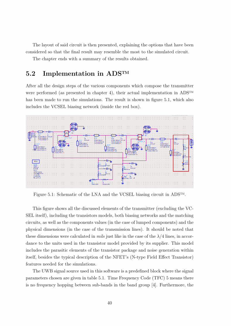
The layout of said circuit is then presented, explaining the options that have beenconsidered so that the final result may resemble the most to the simulated circuit.
The chapter ends with a summary of the results obtained.
5.2 Implementation in ADS™After all the design steps of the various components which compose the transmitterwere performed (as presented in chapter 4), their actual implementation in ADS™has been made to run the simulations. The result is shown in figure 5.1, which alsoincludes the VCSEL biasing network (inside the red box).
Figure 5.1: Schematic of the LNA and the VCSEL biasing circuit in ADS™.
This figure shows all the discussed elements of the transmitter (excluding the VC-SEL itself), including the transistors models, both biasing networks and the matchingcircuits, as well as the components values (in the case of lumped components) and thephysical dimensions (in the case of the transmission lines). It should be noted thatthese dimensions were calculated in mils just like in the case of the λ/4 lines, in accor-dance to the units used in the transistor model provided by its supplier. This modelincludes the parasitic elements of the transistor package and noise generation withinitself, besides the typical description of the NFET’s (N-type Field Effect Transistor)features needed for the simulations.
The UWB signal source used in this software is a predefined block where the signalparameters chosen are given in table 5.1. Time Frequency Code (TFC) 5 means thereis no frequency hopping between sub-bands in the band group [4]. Furthermore, the
40

simulations have been made using a single data frame which in this particular casecorresponds to 18.75 ms of simulation time.
Table 5.1: UWB signal parameters chosen for simulation purposes.
Parameter Value/Type UnitCarrier Frequency 3.432 GHz
Data Rate 200 Mb/sModulation QPSK -Band Group 1 -
Time Frequency Code 5 -
5.3 ADS™ Simulation Results5.3.1 S-Parameters
Some of the S-parameters of the LNA have been obtained in the simulation, namelythe magnitude and phase of S21 (gain) and S11(reflection coefficient) parameters.These results are shown in figures 5.2a, 5.2b and 5.2c, respectively.
From the figure 5.2a one can almost immediately see that the gain is quite constantin the band of the UWB signal, an important characteristic needed to allow for similaramplifier response to the whole signal. Moreover, at 4 GHz the value of the gain is30.7 dB, and 31 dB at a frequency close to the signal’s central one (3.432 GHz). Thegain at 4 GHz is less than the theoretically calculated value, which is 32.2 dB. Thismight have several reasons, starting with the fact that one has designed this LNAusing a unilateral approach which yields an error for the value of each transistor’sgain one actually obtains (refer to subsection 4.3.2), implicating an overall error forthe cascaded transistor system. Despite this being the reason that might contributethe most for the mismatch between gain values, other factors might intervene, suchas: a slight mismatch of the matching circuits at this frequency, because the finetuning was performed to increase the gain at the signal’s frequencies; and the factthat the λ/4 transmission lines used in the biasing network have been designed forthe signal’s central frequency and not for 4 GHz, to work properly at the actualoperating frequencies. Concerning this last choice, it has been observed that if onehad used 4 GHz the gain at this frequency would become 31.1 dB, a slightly highervalue than the original one; however, at 3.432 GHz the gain would diminish, this waydeteriorating the transmitter’s gain at the operating frequencies of interest.
41
The phase of the S21 parameter (figure 5.2b) shows a fairly linear behavior whichtranslates into approximately the same delay at all operating frequencies, particularlyin the UWB signal’s band, indicating that the distortion generation within the devicemight be fairly low.
As far as the S11 parameter (figure 5.2c) is concerned, we can see that its magni-tude ranges between -4.8 dB and -7.1 dB inside the signal’s band, which are relativelyhigh values, with a minimum value of approximately -11.6 dB at 4 GHz. This impliesthat if the maximum allowed power for a wireless UWB signal is inserted into thisamplifier (considering an antenna with unit gain), which is approximately -14.07 dBmor 40 mW [4], the value that will be sent back to the antenna will not exceed 14 mW.As this will hardly ever be the case, because this transmitter will always be at somedistance from the UWB signal source, the actual reflected power will be much lessthan this value.
42
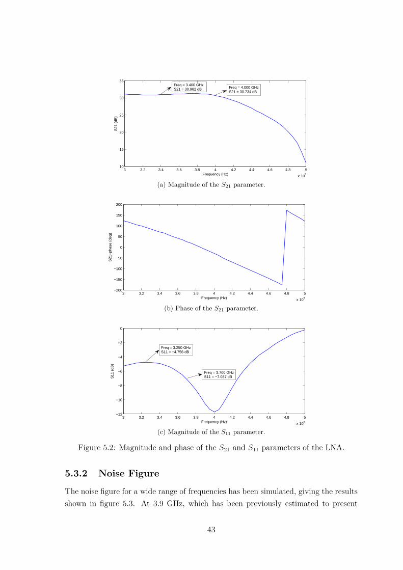
3 3.2 3.4 3.6 3.8 4 4.2 4.4 4.6 4.8 5
x 109
10
15
20
25
30
35
Frequency (Hz)
S21
(dB
)
Freq = 4.000 GHzS21 = 30.734 dB
Freq = 3.400 GHzS21 = 30.982 dB
(a) Magnitude of the S21 parameter.
3 3.2 3.4 3.6 3.8 4 4.2 4.4 4.6 4.8 5
x 109
−200
−150
−100
−50
0
50
100
150
200
Frequency (Hz)
S21
−ph
ase
(deg
)
(b) Phase of the S21 parameter.
3 3.2 3.4 3.6 3.8 4 4.2 4.4 4.6 4.8 5
x 109
−12
−10
−8
−6
−4
−2
0
Frequency (Hz)
S11
(dB
)
Freq = 3.700 GHzS11 = −7.087 dB
Freq = 3.250 GHzS11 = −4.756 dB
(c) Magnitude of the S11 parameter.
Figure 5.2: Magnitude and phase of the S21 and S11 parameters of the LNA.
5.3.2 Noise Figure
The noise figure for a wide range of frequencies has been simulated, giving the resultsshown in figure 5.3. At 3.9 GHz, which has been previously estimated to present
43

a 1 dB noise figure, it actually presents a slightly higher value (1.23 dB), probablydue to the fact that the gain is lower than expected, as concluded in the previoussubsection; also, other noise sources besides the two transistors considered in thecalculations might be present.
It can also be seen that the top value at the signal frequencies is 1.02 dB, a lowvalue as expected.
3 3.2 3.4 3.6 3.8 4 4.2 4.4 4.6 4.8 5
x 109
0
2
4
6
8
10
12
14
Frequency (Hz)
Noi
se F
igur
e (d
B)
Freq = 3.700 GHzNF = 1.020 dB
Freq = 3.900 GHzNF = 1.225 dB
Figure 5.3: Simulated noise figure of the LNA.
5.3.3 Non-Linear Distortion
Non-linear distortion effects in this kind of devices are critical, particularly in OFDM-UWB applications where the signal is known to have a large peak-to-average powerratio. So their study is of extreme importance in order to assess a priori whetherthe transmitter’s distortion effects will be negligible or, otherwise, will considerablyinfluence its performance and decrease the reliability of the link and data quality.
In this way, some of the distortion parameters for the LNA have been simulatedand are presented in table 5.2. These are the intermodulation distortion (IMD)parameters, specifically the input (IIP3) and output (OIP3) third-order interceptpoints and the Spurious-Free Dynamic Range (SFDR).
Table 5.2: Third-order intercept points and SFDR of the transmitter.
Third-order Intercept PointsParameter Value Unit
IIP3 −4.740 dBmOIP3 27.085 dBmSFDR 112.724 dB× Hz 2
3
44

Other distortion studies have been made, namely based on the 1dB compres-sion point, which is just another way of describing when the distortion effects in theLNA will become significant. Figure 5.4 represents the input-to-output power char-acteristics of the amplifier, where the red line represents the linear behavior for thefundamental frequency component and the blue line its compression curve. At the 1dB compression point - where the compression curve deviates by 1 dB from the linearline - the input and output signal powers are indicated in table 5.3.
−70 −60 −50 −40 −30 −20 −10 0−40
−30
−20
−10
0
10
20
30
40
Input Power (dBm)
Out
put P
ower
(dB
m)
Linear
Actual
Figure 5.4: Linear (red) and compression curve (blue) of the LNA.
Table 5.3: 1 dB compression points.
1 dB Compression PointsParameter Value Unit
Input-referred −15.66 dBmOutput-referred 13.92 dBm
In this way, for the maximum allowed input power of -14.07 dBm (for a signal witha 528 MHz bandwidth) the amplifier is operating at approximately 1.6 dB above the 1dB compression point and 9.3 dB far from the IIP3. Thus, IMD spurious are only 18.6dB below the fundamental (see appendix A), and the distortion impairment is alreadysignificant. In real operating conditions, however, where the UWB signal would travelthrough the wireless channel before reaching the transmitter, the signal level wouldbe much lower than this and no intermodulation due to the amplifier is expected.
45

For instance, for a 1 meter wireless link the attenuation would be approximately 43.2dB (refer to appendix B) and in this case the IMD spurious at the output of theamplifier would be approximately 100 dB below the fundamental. As yet anotherexample, the UWB signal spectrum after leaving the source for an input power of -30dBm (approximately 14 cm distance) is shown in figure 5.5a, and the spectrum of thesame signal after passing through the LNA is shown in Figure 5.5b. It can be seenthat both spectra are quite similar because third-order intermodulation distortioncomponents are almost inexistent.
The impact of the VCSEL’s nonlinear distortion on the UWB signal can be seen bycomparing the power spectrum of this signal before (figure 5.5b) and after the VCSEL(figure 5.5c), where distortion effects are now much more visible at frequencies nearthe UWB signal, corresponding to third-order intermodulation distortion components.
2.4 2.6 2.8 3 3.2 3.4 3.6 3.8 4 4.2 4.4
x 109
−110
−100
−90
−80
−70
−60
−50
−40
−30
−20
−10
0
Frequency (Hz)
Spe
ctru
m (
dBm
)
(a) UWB signal source spectrum.
2.4 2.6 2.8 3 3.2 3.4 3.6 3.8 4 4.2 4.4
x 109
−80
−70
−60
−50
−40
−30
−20
−10
0
Frequency (Hz)
Spe
ctru
m (
dBm
)
(b) UWB signal spectrum after passing through theLNA.
2.4 2.6 2.8 3 3.2 3.4 3.6 3.8 4 4.2 4.4
x 109
−140
−130
−120
−110
−100
−90
−80
−70
−60
Frequency (Hz)
Spe
ctru
m (
dBm
)
(c) UWB signal spectrum after passing through theLNA and the VCSEL.
Figure 5.5: UWB signal spectra after several transmission stages for an input powerof -30 dBm.
5.3.4 Error Vector Magnitude (EVM)
In order to fully assess the performance of the whole transmitter, EVM simulationshave been made by means of ADS™ and Matlab™ co-simulations, as already men-tioned. A block diagram of the setup used for these co-simulations is depicted in
46
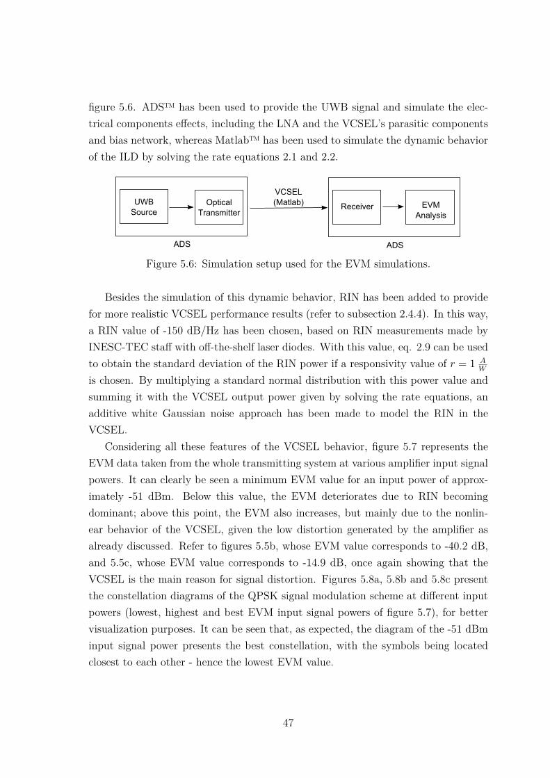
figure 5.6. ADS™ has been used to provide the UWB signal and simulate the elec-trical components effects, including the LNA and the VCSEL’s parasitic componentsand bias network, whereas Matlab™ has been used to simulate the dynamic behaviorof the ILD by solving the rate equations 2.1 and 2.2.
UWB
Source
Optical
TransmitterReceiver EVM
Analysis
VCSEL
(Matlab)
ADS ADS
Figure 5.6: Simulation setup used for the EVM simulations.
Besides the simulation of this dynamic behavior, RIN has been added to providefor more realistic VCSEL performance results (refer to subsection 2.4.4). In this way,a RIN value of -150 dB/Hz has been chosen, based on RIN measurements made byINESC-TEC staff with off-the-shelf laser diodes. With this value, eq. 2.9 can be usedto obtain the standard deviation of the RIN power if a responsivity value of r = 1 A
W
is chosen. By multiplying a standard normal distribution with this power value andsumming it with the VCSEL output power given by solving the rate equations, anadditive white Gaussian noise approach has been made to model the RIN in theVCSEL.
Considering all these features of the VCSEL behavior, figure 5.7 represents theEVM data taken from the whole transmitting system at various amplifier input signalpowers. It can clearly be seen a minimum EVM value for an input power of approx-imately -51 dBm. Below this value, the EVM deteriorates due to RIN becomingdominant; above this point, the EVM also increases, but mainly due to the nonlin-ear behavior of the VCSEL, given the low distortion generated by the amplifier asalready discussed. Refer to figures 5.5b, whose EVM value corresponds to -40.2 dB,and 5.5c, whose EVM value corresponds to -14.9 dB, once again showing that theVCSEL is the main reason for signal distortion. Figures 5.8a, 5.8b and 5.8c presentthe constellation diagrams of the QPSK signal modulation scheme at different inputpowers (lowest, highest and best EVM input signal powers of figure 5.7), for bettervisualization purposes. It can be seen that, as expected, the diagram of the -51 dBminput signal power presents the best constellation, with the symbols being locatedclosest to each other - hence the lowest EVM value.
47

−90 −80 −70 −60 −50 −40 −30−45
−40
−35
−30
−25
−20
−15
−10
−5
Input Power (dBm)
EV
M (
dB)
Figure 5.7: Transmitter EVM results for different input power values.
(a) Constellation diagram for an input signal powerof -51 dBm.
(b) Constellation diagram for an input signal powerof -83 dBm.
(c) Constellation diagram for an input signal powerof -30 dBm.
Figure 5.8: Constellation diagrams of the UWB signal after passing through theoptical transmitter, using different input powers.
If we consider an EVM value of -10 dB [29] to be sufficient for reliable data
48
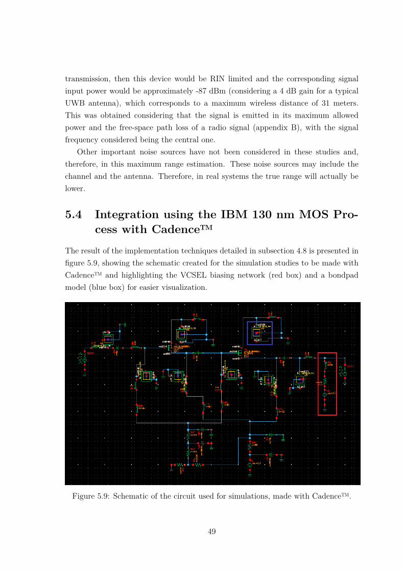
transmission, then this device would be RIN limited and the corresponding signalinput power would be approximately -87 dBm (considering a 4 dB gain for a typicalUWB antenna), which corresponds to a maximum wireless distance of 31 meters.This was obtained considering that the signal is emitted in its maximum allowedpower and the free-space path loss of a radio signal (appendix B), with the signalfrequency considered being the central one.
Other important noise sources have not been considered in these studies and,therefore, in this maximum range estimation. These noise sources may include thechannel and the antenna. Therefore, in real systems the true range will actually belower.
5.4 Integration using the IBM 130 nm MOS Pro-cess with Cadence™
The result of the implementation techniques detailed in subsection 4.8 is presented infigure 5.9, showing the schematic created for the simulation studies to be made withCadence™ and highlighting the VCSEL biasing network (red box) and a bondpadmodel (blue box) for easier visualization.
Figure 5.9: Schematic of the circuit used for simulations, made with Cadence™.
49

The model used for the transistors is a N-type FET provided by the technologylibrary. The model used for the bondpads is also provided by the technology library(presenting a 17 fF capacitance) and the bonding wire is modeled by a 1 nH seriesinductor, which have been inserted in all the places of the circuit that will need tohave outside connections (pins). The elements that are left inside the circuit arealimited by the bondpads make the integrable circuit, which can only be composed ofsmall components and the transistors in order to avoid creating a large IC.
As far as the input impedance matching components is concerned, a 5 pF capacitor(CG) has been used together with a 4 nH series inductor (LG), obtained by tuning.At the output, the DC-coupled capacitor Cout also has 5 pF, enough to obtain goodimpedance matching without severely attenuating the signals.
5.5 Cadence™ Simulation Results5.5.1 S-Parameters
Just like it was done for the discrete LNA, the main S-parameters of the circuitdesigned with Cadence™ have also been obtained.
It can be seen from figure 5.10a that the gain of the amplifier is not flat, being amaximum 31.1 dB in the lower operating frequencies and decreasing until 29.1 dB atthe top frequency limit. Despite this meaning a 2 dB difference between gains in theoperating signal range, it is still below the 3 dB limit (cut-off frequency definition),making it acceptable. However, it is worse than the behavior obtained in the casewith discrete components but, once again, the design conditions are quite differentand a very similar behavior should not be expected.
From the S21 phase results (figure 5.10b), it can be seen that it does not present avery linear behavior and that it might, therefore, distort more the transmitting signalas it passes through the device than the other version.
As far as the S11 result is concerned, its magnitude is presented in figure 5.10cwhich indicates a quite small value for the top frequencies (-16.8 dB), whereas thisincreases as the frequency becomes smaller, ultimately yielding -3.1 dB for the lowerfrequency limit. This is a relatively large value, which might impose future stabilityproblems. However, it has been found that the transmitter is unconditionally stableat these frequencies, having a stability factor of K = 1.04 and ∆ = 0.79. But theamount of reflected signal back to the antenna could become quite large if the inputpower approaches the maximum allowed – i.e., if this device is placed close to theemitting one.
50
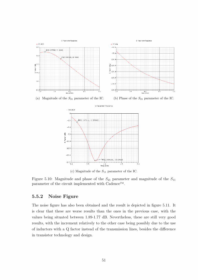
(a) Magnitude of the S21 parameter of the IC. (b) Phase of the S21 parameter of the IC.
(c) Magnitude of the S11 parameter of the IC.
Figure 5.10: Magnitude and phase of the S21 parameter and magnitude of the S11parameter of the circuit implemented with Cadence™.
5.5.2 Noise Figure
The noise figure has also been obtained and the result is depicted in figure 5.11. Itis clear that these are worse results than the ones in the previous case, with thevalues being situated between 1.89-1.77 dB. Nevertheless, these are still very goodresults, with the increment relatively to the other case being possibly due to the useof inductors with a Q factor instead of the transmission lines, besides the differencein transistor technology and design.
51
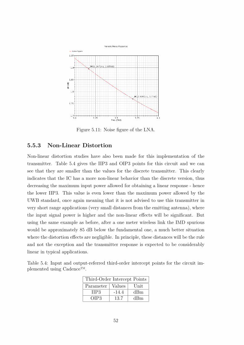
Figure 5.11: Noise figure of the LNA.
5.5.3 Non-Linear Distortion
Non-linear distortion studies have also been made for this implementation of thetransmitter. Table 5.4 gives the IIP3 and OIP3 points for this circuit and we cansee that they are smaller than the values for the discrete transmitter. This clearlyindicates that the IC has a more non-linear behavior than the discrete version, thusdecreasing the maximum input power allowed for obtaining a linear response - hencethe lower IIP3. This value is even lower than the maximum power allowed by theUWB standard, once again meaning that it is not advised to use this transmitter invery short range applications (very small distances from the emitting antenna), wherethe input signal power is higher and the non-linear effects will be significant. Butusing the same example as before, after a one meter wireless link the IMD spuriouswould be approximately 85 dB below the fundamental one, a much better situationwhere the distortion effects are negligible. In principle, these distances will be the ruleand not the exception and the transmitter response is expected to be considerablylinear in typical applications.
Table 5.4: Input and output-referred third-order intercept points for the circuit im-plemented using Cadence™.
Third-Order Intercept PointsParameter Values Unit
IIP3 -14.4 dBmOIP3 13.7 dBm
52
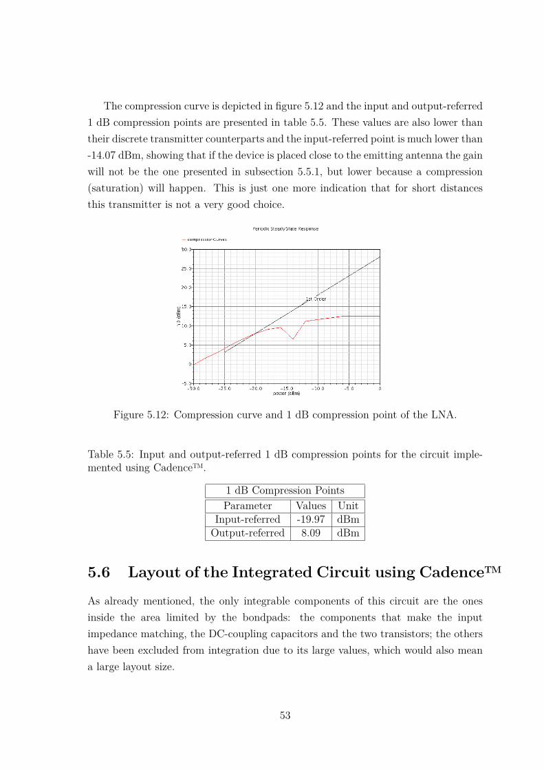
The compression curve is depicted in figure 5.12 and the input and output-referred1 dB compression points are presented in table 5.5. These values are also lower thantheir discrete transmitter counterparts and the input-referred point is much lower than-14.07 dBm, showing that if the device is placed close to the emitting antenna the gainwill not be the one presented in subsection 5.5.1, but lower because a compression(saturation) will happen. This is just one more indication that for short distancesthis transmitter is not a very good choice.
Figure 5.12: Compression curve and 1 dB compression point of the LNA.
Table 5.5: Input and output-referred 1 dB compression points for the circuit imple-mented using Cadence™.
1 dB Compression PointsParameter Values Unit
Input-referred -19.97 dBmOutput-referred 8.09 dBm
5.6 Layout of the Integrated Circuit using Cadence™As already mentioned, the only integrable components of this circuit are the onesinside the area limited by the bondpads: the components that make the inputimpedance matching, the DC-coupling capacitors and the two transistors; the othershave been excluded from integration due to its large values, which would also meana large layout size.
53
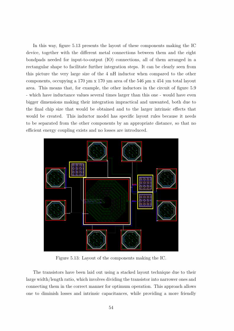
In this way, figure 5.13 presents the layout of these components making the ICdevice, together with the different metal connections between them and the eightbondpads needed for input-to-output (IO) connections, all of them arranged in arectangular shape to facilitate further integration steps. It can be clearly seen fromthis picture the very large size of the 4 nH inductor when compared to the othercomponents, occupying a 170 mm x 170 mm area of the 546 mm x 454 mm total layoutarea. This means that, for example, the other inductors in the circuit of figure 5.9- which have inductance values several times larger than this one - would have evenbigger dimensions making their integration impractical and unwanted, both due tothe final chip size that would be obtained and to the larger intrinsic effects thatwould be created. This inductor model has specific layout rules because it needsto be separated from the other components by an appropriate distance, so that noefficient energy coupling exists and no losses are introduced.
Figure 5.13: Layout of the components making the IC.
The transistors have been laid out using a stacked layout technique due to theirlarge width/length ratio, which involves dividing the transistor into narrower ones andconnecting them in the correct manner for optimum operation. This approach allowsone to diminish losses and intrinsic capacitances, while providing a more friendly
54
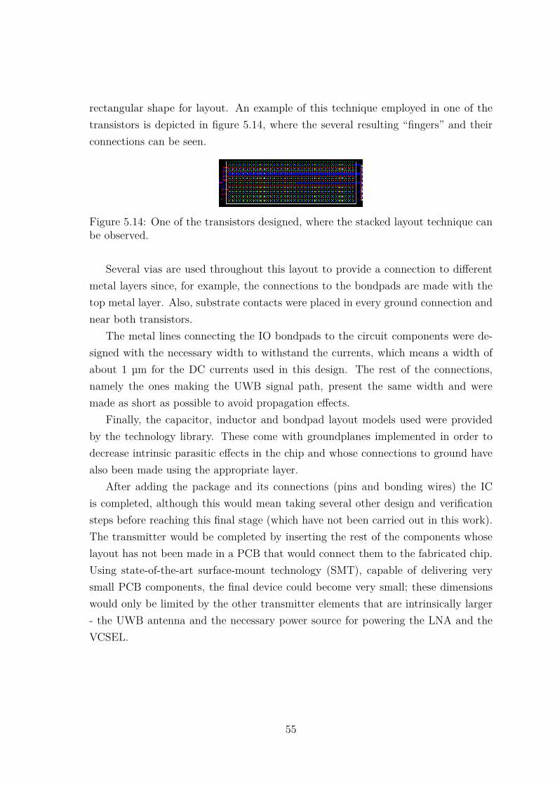
rectangular shape for layout. An example of this technique employed in one of thetransistors is depicted in figure 5.14, where the several resulting “fingers” and theirconnections can be seen.
Figure 5.14: One of the transistors designed, where the stacked layout technique canbe observed.
Several vias are used throughout this layout to provide a connection to differentmetal layers since, for example, the connections to the bondpads are made with thetop metal layer. Also, substrate contacts were placed in every ground connection andnear both transistors.
The metal lines connecting the IO bondpads to the circuit components were de-signed with the necessary width to withstand the currents, which means a width ofabout 1 µm for the DC currents used in this design. The rest of the connections,namely the ones making the UWB signal path, present the same width and weremade as short as possible to avoid propagation effects.
Finally, the capacitor, inductor and bondpad layout models used were providedby the technology library. These come with groundplanes implemented in order todecrease intrinsic parasitic effects in the chip and whose connections to ground havealso been made using the appropriate layer.
After adding the package and its connections (pins and bonding wires) the ICis completed, although this would mean taking several other design and verificationsteps before reaching this final stage (which have not been carried out in this work).The transmitter would be completed by inserting the rest of the components whoselayout has not been made in a PCB that would connect them to the fabricated chip.Using state-of-the-art surface-mount technology (SMT), capable of delivering verysmall PCB components, the final device could become very small; these dimensionswould only be limited by the other transmitter elements that are intrinsically larger- the UWB antenna and the necessary power source for powering the LNA and theVCSEL.
55
5.7 SummaryThis chapter dealt with the implementation of the circuits and with the varioussimulation results obtained both with ADS™ and Cadence™, which gave a glimpseon how the different versions of the transmitter will behave if put to use in realconditions.
This being said, the discrete transmitter presents a stable gain around 31 dBthroughout the entire UWB signal frequency range, although being a bit lower thanits estimated gain. Its noise figure tops 1 dB at the maximum signal frequency, avery good value even when not considering the VCSEL noise in this result. Thenon-linear distortions caused by the circuit have been found not to be significantat real-life operating conditions, meaning this device will not affect severely the databeing transmitted. However, when considering the VCSEL dynamic behavior in EVMsimulations, one has found that the device presents an optimum input signal power(-51 dBm) at which the corresponding EVM value is a minimum and that this valueis bounded by the ensemble’s noise at lower powers and by the VCSEL distortion forhigher input powers.
On the other hand, the IC version of the transmitter was first implemented andsimulated as an analogue microelectronics circuit and considering some effects thatonly these circuits present, like the bondpads’ and bonding wires’ intrinsic behavior.The results show a circuit with overall results worse than the discrete version, specifi-cally: the varying gain along the operating signal frequencies (going from 31.1 to 29.1dB); the higher noise figure (around 1.8 dB) not considering the VCSEL RIN; and,the lower IIP3, OIP3 and 1 dB compression points resulting in higher distortion ofthe signals.
Its layout has then been made, taking into account all the necessary rules in orderto avoid introducing into the chip even more unwanted intrinsic effects than the onesalready considered. The layout yielded a low complexity and small size IC, whoselayout measures just 546 mm x 454 mm. The final device size would only depend onthe external components that are needed for this transmitter to work, like the powersource and the antenna.
56
Chapter 6
Conclusion
The main goal of this thesis was to design and simulate an optical transmitter forUWB signals based on discrete COTS components and MOS technology. Consideringtheir simulated properties and expected behavior under future possible applications,I believe this goal has been achieved.
The thesis itself presented several chapters before delivering the final results.Chapter 1 gave a short introduction to the entire work, briefly presenting its mo-tivations and goals as well as somewhat similar projects recently developed by groupsworldwide.
In chapter 2 the main features of the RoF systems have been presented, as well assome of the features of UWB signals. Moreover, the structure, properties and modelused to simulate the VCSEL have also been explained, including the RIN these lasersusually present.
In chapter 3 the design techniques to obtain RF amplifiers have been explained,whereas in chapter 4 these have been applied to design both versions of the desiredtransmitter and to estimate some of their properties.
In chapter 5 their actual implementation and simulation using either ADS™ orCadence™ has been performed, extracting the main properties for behavior assess-ment.
Specifically speaking about the final results, the discrete transmitter is a lowcomplexity device with a high gain and very low noise figure, whose response in realapplications can be considerably linear. This device has been simulated with a specific200 Mb/s QPSK-modulated UWB signal and typical VCSEL parameters, giving amaximum estimated range of 31 meters and limited only by the VCSEL RIN, a valuethat is suitable for most of the desired applications. In reality this range will, however,be reduced due to the existence of other noise sources and wireless channel effects.
57
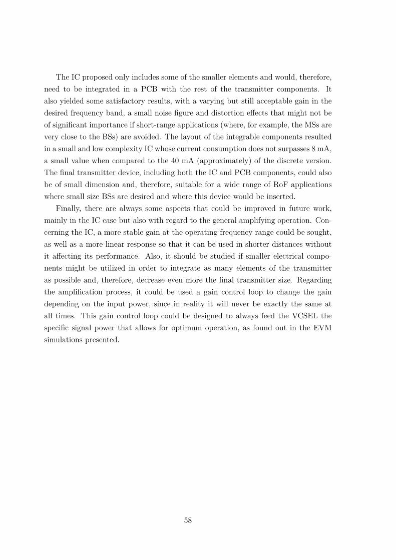
The IC proposed only includes some of the smaller elements and would, therefore,need to be integrated in a PCB with the rest of the transmitter components. Italso yielded some satisfactory results, with a varying but still acceptable gain in thedesired frequency band, a small noise figure and distortion effects that might not beof significant importance if short-range applications (where, for example, the MSs arevery close to the BSs) are avoided. The layout of the integrable components resultedin a small and low complexity IC whose current consumption does not surpasses 8 mA,a small value when compared to the 40 mA (approximately) of the discrete version.The final transmitter device, including both the IC and PCB components, could alsobe of small dimension and, therefore, suitable for a wide range of RoF applicationswhere small size BSs are desired and where this device would be inserted.
Finally, there are always some aspects that could be improved in future work,mainly in the IC case but also with regard to the general amplifying operation. Con-cerning the IC, a more stable gain at the operating frequency range could be sought,as well as a more linear response so that it can be used in shorter distances withoutit affecting its performance. Also, it should be studied if smaller electrical compo-nents might be utilized in order to integrate as many elements of the transmitteras possible and, therefore, decrease even more the final transmitter size. Regardingthe amplification process, it could be used a gain control loop to change the gaindepending on the input power, since in reality it will never be exactly the same atall times. This gain control loop could be designed to always feed the VCSEL thespecific signal power that allows for optimum operation, as found out in the EVMsimulations presented.
58

References
[1] H. B. Kim, “Radio over fiber based network architecture,” Ph.D. dissertation,Technischen Universitat Berlin, October 2005.
[2] H. M. Salgado, J. M. B. Oliveira, and N. Lima, “Modelling optical/RF im-pairments in ultra-wideband radio over fiber,” Photonic Components for Ultra-Wideband Radio over Optical Fiber (UROOF), Tech. Rep., 2008.
[3] D. Pozar, Microwave Engineering, , 3rd edition ed. Wiley, 2005.
[4] Standard ECMA-368: High Rate UltraWideband PHY and MAC Standard, 3rdEdition, ECMA International Std., December 2008.
[5] D. Porcino and W. Hirt, “Ultra-wideband radio technology: Potential and chal-lenges ahead,” IEEE Communications Magazine, July 2003.
[6] K. Siwiak, “Ultra-wide band radio: introducing a new technology,” in VehicularTechnology Conference, 2001. VTC 2001 Spring. IEEE VTS 53rd, vol. 2. IEEE,2001, pp. 1088–1093.
[7] T. Quinlan, M. Morant, S. Dudley, R. Llorente, and S. Walker, “480-Mbit/sUWB bi-directional radio over fiber CWDM PON using ultra-low cost and powerVCSELs,” Optics Express, vol. 19, no. 26, pp. B197–B202, 2011.
[8] D. Watanabe, A. Ono, and T. Okayasu, “CMOS optical 4-PAM VCSEL driverwith modal-dispersion equalizer for 10-Gb/s 500m MMF transmission,” in Solid-State Circuits Conference-Digest of Technical Papers, 2009. ISSCC 2009. IEEEInternational. IEEE, 2009, pp. 106–107.
[9] W. Oh and K. Park, “Design of a 4-channel 10-Gb/s CMOS VCSEL driver array,”in Optical Internet, 2008. COIN 2008. 7th International Conference on. IEEE,2008, pp. 1–2.
59

[10] S. Palermo and M. Horowitz, “High-speed transmitters in 90nm CMOS for high-density optical interconnects,” European Solid-State Circuits Conference, pp.508–511, 2006.
[11] M. Beltran, J. Jensen, X. Yu, R. Llorente, R. Rodes, M. Ortsiefer, C. Neumeyr,and I. Monroy, “Performance of a 60-GHz DCM-OFDM and BPSK-impulseultra-wideband system with radio-over-fiber and wireless transmission employinga directly-modulated VCSEL,” Selected Areas in Communications, IEEE Jour-nal on, vol. 29, no. 6, pp. 1295 –1303, june 2011.
[12] D. Opatic and G. Croatia, “Radio over fiber technology for wireless access,”Ericsson Nikola Tesla dd, Krapinska, vol. 45, 2009.
[13] A. Ngoma, “Radio-over-fibre technology for broadband wireless communicationsystems,” Ph.D. dissertation, Technische Universiteit Eindhoven, 2005.
[14] C. Lim, A. Nirmalathas, M. Bakaul, P. Gamag, K.-L. Lee, D. N. Y. Yang, andR. Waterhouse, “Fiber-wireless networks and subsystem technologies,” Journalof Lightwave Technology, vol. 28, pp. 390–405, 2010.
[15] http://www.rp-photonics.com (Encyclopedia of Laser Physics and Technology).(December 2011) Rp-photonics.
[16] K. Iga, “Surface-emitting laser: Its birth and generation of new optoelectronicsfield,” IEEE Journal on Selected Topics in Quantum Electronics, vol. vol. 6,no. 6, November/December 2000.
[17] L. A. Coldren and S. W. Corzine, Diode Lasers and Photonic Integrated Circuits.John Wiley and Sons, Inc, 1999.
[18] C. Wilmsen, H. Temkin, and L. Coldren, Vertical-Cavity Surface-EmittingLasers: Design, Fabrication, Characterization, and Applications. CambridgeUniversity Press, 1999.
[19] M. Bruensteiner and G. C. Papen, “Extraction of VCSEL rate-equation param-eters for low-bias system simulation,” IEEE J. of Selected Topics in QuantumElectronics, vol. 5, pp. 487 – 494, 1999.
60

[20] H. M. Salgado, “Performance assessment of subcarrier multiplexed optical sys-tems: Implications of laser nonlinearities,” Ph.D. dissertation, School of Elec-tronic Engineering and Computer Systems, University of Wales, Bangor, UK,November 1993.
[21] C. H. Cox III, Analog Optical Links - Theory and Practice. Cambridge UniversityPress, 2004.
[22] H. M. Salgado, Lectures of "Engenharia de RF e Microondas". Faculdade deEngenharia da Universidade do Porto, 2011.
[23] R. Gilmore and L. Besser, Practical RF Circuit Design for Modern WirelessSystems: Active Circuits and Systems. Artech House, Inc., 2003, vol. II.
[24] A. Sedra and K. Smith, Microeletronic Circuits, 4th ed. Oxford UniversityPress, 1998.
[25] J. Machado da Silva, Lectures of “Microelectrónica Analógica”. Faculdade deEngenharia da Universidade do Porto, 2011.
[26] Data Sheet: ATF-55143 - Low Noise Enhancement Mode Pseudomorphic HEMTin a Surface Mount Plastic Package, Avago Technologies.
[27] I. M. Division, “Foundry technologies: 130-nm CMOS and RF CMOS,” IBM,Tech. Rep., 2003.
[28] IBM Foundry and Manufacturing Services Education: CMOS8RF(CMRF8SF)Design Kit Training V1.3.1.0.
[29] L. Pessoa, D. Coelho, J. Oliveira, J. C. S. Castro, and H. M. Salgado, “Exper-imental evaluation of R-EAM performance in RoF networks,” in InternationalSymposium on Green Radio over Fibre & All Optical Technologies for WirelessAccess Networks, June 2011.
[30] A. B. Carlson and P. B. Crilly, Communication Systems: An Introduction toSignals and Noise in Electrical Communication, 5th ed. McGraw-Hill, 2010.
61
Appendix A
Power Relation Between Spuriousand Fundamental ComponentsThrough IntermodulationDistortion
In figure A.1 is represented the input-to-output power characteristics of a genericnon-linear system.
Pin(dBm)
Pout(dBm)
N0
P2w1-w2
Pw1
ΔP
OIP3
Figure A.1: Input-to-output power characteristics of a non-linear system.
In order to find out the relative power of the spurious when compared to thefundamental frequency component, assuming this fundamental component’s power isstill in the linear region, one must first know the relation between their linear powercharacteristics [22],
P2ω1−ω2 = 3Pω1 − 2P3 (A.1)
62
From figure A.1 it is easy to relate Pω1to the output third-order interception pointOIP3
Pω1 = P3 −∆P (A.2)
which by introducing in eq. A.1 yields
P2ω1−ω2 = 3P3 − 3∆P − 2P3
= P3 − 3∆P
Using once more the eq. A.2 we obtain the desired relation between the powersof the frequency components
Pω1 − P2ω1−ω2 = 2∆P
63
Appendix B
Free-Space Path Loss
The Friis radio link formula addresses the issue of how much signal power is receivedat an isotropic antenna after being transmitted by another antenna and free-spacepropagated. This formula can be expressed as [3]
Pr = GtGrλ2
(4πl)2 Pt (B.1)
where Pr and Pt are the received and transmitted powers, respectively, Gt and Gr
are the receiving and transmitting isotropic antenna gains, respectively, λ is the radiosignal free-space wavelength and l is the distance between antennas. This formuladoes not include important and realistic phenomena which occur in every wirelesspropagation, like medium absorption, scattering and multipath effects, which woulddiminish the amount of power received. It only considers the losses and effectiveaperture areas of the antenna and signal power loss due to spherical dispersion of theenergy with travelled distance.
If one takes eq. B.1 and consider both antenna gains to be unitary, Gt = Gr = 1,then one gets the free-space path loss (L) of a radio signal [30]
L = PtPr
=(
4πlλ
)2
=(
4πlfc
)2
(B.2)
where f is the signal’s frequency.Eq. B.2 becomes
FSPL(dB) = 20log10(l) + 20log10(f)− 27.55
if expressed in dB, with l in meters and f in megahertz.
64