بسم الله الرحمن الرحيم Lecture( 6) Data Modeling Using the Entity-Relationship (ER) Model 1.
Upload
radha-vinchurkarCategory
view
229download
0
8/7/2019 Lecture 2 Transistor Modeling
http://slidepdf.com/reader/full/lecture-2-transistor-modeling 1/44
Hardware Modeling S.M.Lambor 1
Hardware Modeling
Modeling of Transistor
8/7/2019 Lecture 2 Transistor Modeling
http://slidepdf.com/reader/full/lecture-2-transistor-modeling 2/44
Hardware Modeling S.M.Lambor 2
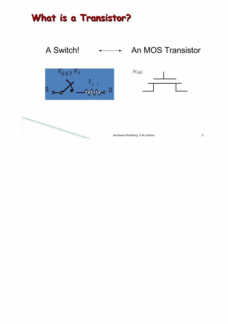
What is a Transistor?What is a Transistor?
V G S
≥ V T
R o n
S D
A Switch!
|VGS|
An MOS Transistor
8/7/2019 Lecture 2 Transistor Modeling
http://slidepdf.com/reader/full/lecture-2-transistor-modeling 3/44
Hardware Modeling S.M.Lambor 3
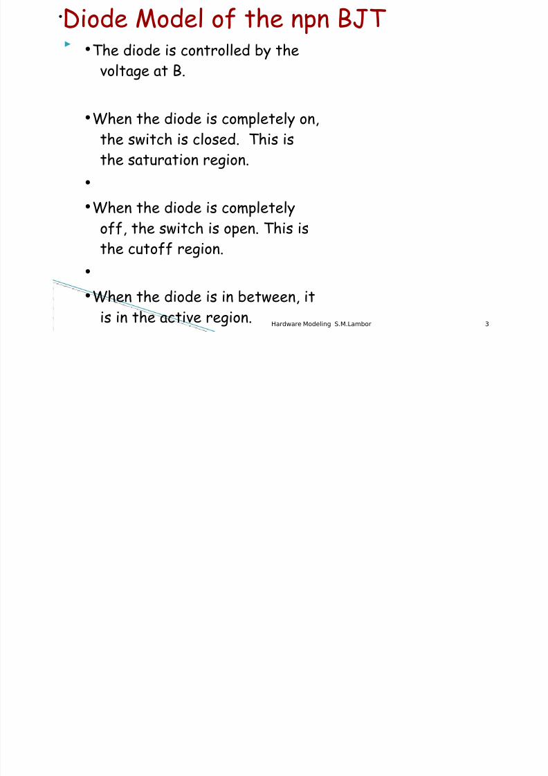
Diode Model of the npn BJT •The diode is controlled by the
voltage at B.
•When the diode is completely on,the switch is closed. This is
the saturation region.•
•When the diode is completely
off, the switch is open. This isthe cutoff region.
•
•When the diode is in between, it
is in the active region.

8/7/2019 Lecture 2 Transistor Modeling
http://slidepdf.com/reader/full/lecture-2-transistor-modeling 4/44
Hardware Modeling S.M.Lambor 4
Switch Model of the npn BJT
Controlstransistor Switch
Circuit that isswitched
Remove the part of the circuit that controls the switch andconsider two possible cases:

8/7/2019 Lecture 2 Transistor Modeling
http://slidepdf.com/reader/full/lecture-2-transistor-modeling 5/44
Hardware Modeling S.M.Lambor 5
Current-Voltage RelationsCurrent-Voltage Relations
A good transistorA good transistor
QuadraticRelationship
0 0.5 1 1.5 2 2.50
1
2
3
4
5
6x 10
-4
VDS
(V)
I D
( A )
VGS= 2.5 V
VGS= 2.0 V
VGS= 1.5 V
VGS= 1.0 V
Resistive Saturation
VDS = VGS - VT

8/7/2019 Lecture 2 Transistor Modeling
http://slidepdf.com/reader/full/lecture-2-transistor-modeling 6/44
Hardware Modeling S.M.Lambor 6
Current-Voltage RelationsCurrent-Voltage Relations
The Deep-Submicron EraThe Deep-Submicron Era
Linear Relationship
-4
VDS
(V)
0 0.5 1 1.5 2 2.50
0.5
1
1.5
2
2.5x 10
I D
( A )
VGS= 2.5 V
VGS= 2.0 V
VGS= 1.5 V
VGS= 1.0 V
Early Saturation

8/7/2019 Lecture 2 Transistor Modeling
http://slidepdf.com/reader/full/lecture-2-transistor-modeling 7/44Hardware Modeling S.M.Lambor 7
Schematic Symbols and Sign ConventionsSchematic Symbols and Sign Conventions
C
E
B
I B
I E
I C +
–
+
+
–
–
V BC
V BE
V CE
C
E
B
I B
I E
I C +
–
+
+
–
–
V BC
V BE
V CE
(a) npn (b) pnp

8/7/2019 Lecture 2 Transistor Modeling
http://slidepdf.com/reader/full/lecture-2-transistor-modeling 8/44Hardware Modeling S.M.Lambor 8
Operations ModesOperations Modes

8/7/2019 Lecture 2 Transistor Modeling
http://slidepdf.com/reader/full/lecture-2-transistor-modeling 9/44Hardware Modeling S.M.Lambor 9
Forward Active OperationForward Active Operation
x
E B C
W B
Carrier Concentration
Depletion
Regions
0 W
pe0
pc0
n b0
n b(0)

8/7/2019 Lecture 2 Transistor Modeling
http://slidepdf.com/reader/full/lecture-2-transistor-modeling 10/44Hardware Modeling S.M.Lambor 10
Reverse ActiveReverse Active
x
E B C
W B
Carrier Concentration
0 W
pe0
n b0
n b(0)
pc0
n b(W)
8/7/2019 Lecture 2 Transistor Modeling
http://slidepdf.com/reader/full/lecture-2-transistor-modeling 11/44Hardware Modeling S.M.Lambor 11
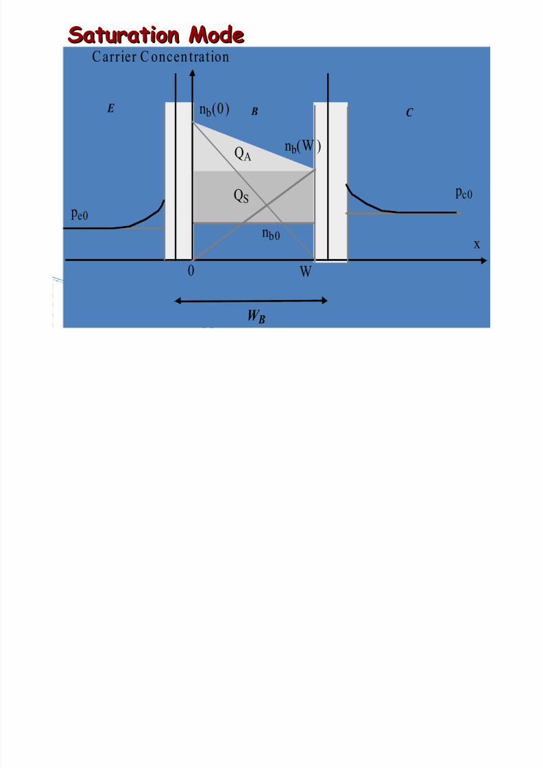
Saturation ModeSaturation Mode
x
E B C
W B
C arrier C oncen tration
0 W
pe0
n b0
n b(0)
pc0QS
QAn b
(W )
8/7/2019 Lecture 2 Transistor Modeling
http://slidepdf.com/reader/full/lecture-2-transistor-modeling 12/44Hardware Modeling S.M.Lambor 12
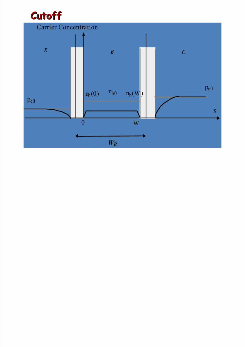
CutoffCutoff
x
E B C
W B
Carrier Concentration
0 W
pe0
n b0n b(0) pc0
n b(W)

8/7/2019 Lecture 2 Transistor Modeling
http://slidepdf.com/reader/full/lecture-2-transistor-modeling 13/44Hardware Modeling S.M.Lambor 13
A Model for Manual AnalysisA Model for Manual Analysis
E
C B
βF I B
I B
+
–
V BE
I B = I S (eV BE /φT – 1)
E
C B
βF I B
I B
+ –
V BE (on )
(a) Forward-active (b) Forward-active (simplified)
E
C B
I B
+ –V BE (sat )
(c) Forward-saturation
+ – V CE (sat )
I C
< βFI B

8/7/2019 Lecture 2 Transistor Modeling
http://slidepdf.com/reader/full/lecture-2-transistor-modeling 14/44Hardware Modeling S.M.Lambor 14
Capacitive Model for Bipolar TransistorCapacitive Model for Bipolar TransistorC
E
B
QF
QR
C be
C bc
S
C cs
collector-substrate
junction capacitance
base-emitter
base-collector junction capacitances
base charge

8/7/2019 Lecture 2 Transistor Modeling
http://slidepdf.com/reader/full/lecture-2-transistor-modeling 15/44Hardware Modeling S.M.Lambor 15
Base Charge - Diffusion CapacitanceBase Charge - Diffusion Capacitance

8/7/2019 Lecture 2 Transistor Modeling
http://slidepdf.com/reader/full/lecture-2-transistor-modeling 16/44Hardware Modeling S.M.Lambor 16
Bipolar Transistors - Secondary EffectsBipolar Transistors - Secondary Effects
• Early Voltage
• Parasitic Resistances
• Beta Variations

8/7/2019 Lecture 2 Transistor Modeling
http://slidepdf.com/reader/full/lecture-2-transistor-modeling 17/44Hardware Modeling S.M.Lambor 17
Early VoltageEarly Voltage
Forward
Active
Saturation
VA
V CE
I C
V BE3
V BE2
V BE1

8/7/2019 Lecture 2 Transistor Modeling
http://slidepdf.com/reader/full/lecture-2-transistor-modeling 18/44
Hardware Modeling S.M.Lambor 18
Modeling of Amplifier

8/7/2019 Lecture 2 Transistor Modeling
http://slidepdf.com/reader/full/lecture-2-transistor-modeling 19/44
Hardware Modeling S.M.Lambor 19
The BJT is an an excellent amplifier when biasedin the forward-active region.
The FET can be used as an amplifier if operated inthe saturation region.
In these regions, the transistors can provide high
voltage, current and power gains. DC bias is provided to stabilize the operating point
in the desired operation region. The DC Q-point also determines
◦ The small-signal parameters of the transistor◦ The voltage gain, input resistance, and output resistance◦ The maximum input and output signal amplitudes◦ The overall power consumption of the amplifier

8/7/2019 Lecture 2 Transistor Modeling
http://slidepdf.com/reader/full/lecture-2-transistor-modeling 20/44
Hardware Modeling S.M.Lambor 20
A Simple BJT AmplifierA Simple BJT Amplifier
The BJT is biased in the forward active region by dc voltage sources V BE
and V CC = 10 V. The DC Q-point is set at, (V CE , I C ) = (5 V, 1.5 mA) with I B= 15 µ A.
Total base-emitter voltage is:
Collector-emitter voltage is: This produces a load line.

8/7/2019 Lecture 2 Transistor Modeling
http://slidepdf.com/reader/full/lecture-2-transistor-modeling 21/44
21
BJT Amplifier (continued)BJT Amplifier (continued)
An 8 mV peak change in v BE gives a 5 µ A change in i B and a
0.5 mA change in iC .
The 0.5 mA change in iC gives a 1.65 V change in vCE .
If changes in operating currentsand voltages are small enough,
then I C and V CE waveforms areundistorted replicas of the inputsignal.
A small voltage change at the base causes a large voltage
change at the collector. Thevoltage gain is given by:
The minus sign indicates a 1800 phase shift between input andoutput signals.
8/7/2019 Lecture 2 Transistor Modeling
http://slidepdf.com/reader/full/lecture-2-transistor-modeling 22/44
Hardware Modeling S.M.Lambor 22
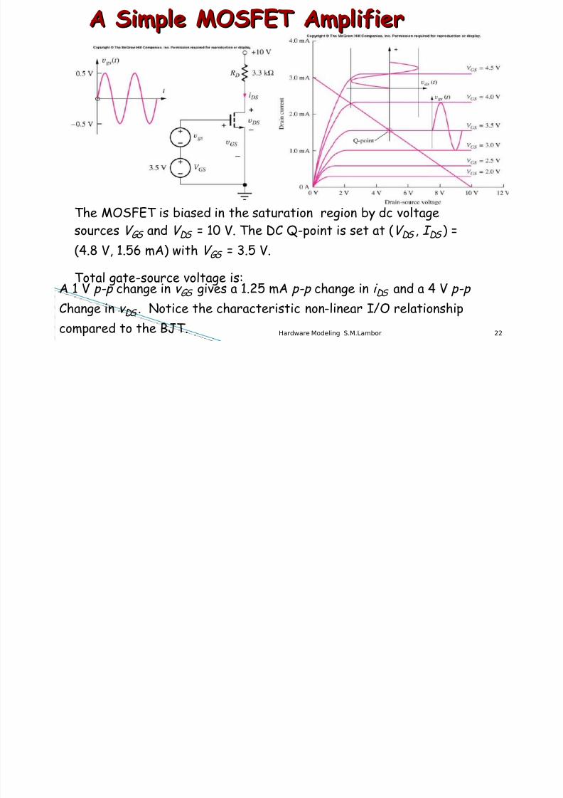
A Simple MOSFET AmplifierA Simple MOSFET Amplifier
The MOSFET is biased in the saturation region by dc voltagesources V GS and V DS = 10 V. The DC Q-point is set at (V DS , I DS ) =
(4.8 V, 1.56 mA) with V GS = 3.5 V.
Total gate-source voltage is:A 1 V p-p change in v GS gives a 1.25 mA p-p change in i DS and a 4 V p-p
Change in v DS . Notice the characteristic non-linear I/O relationship
compared to the BJT.

8/7/2019 Lecture 2 Transistor Modeling
http://slidepdf.com/reader/full/lecture-2-transistor-modeling 23/44
Hardware Modeling S.M.Lambor 23
AC coupling through capacitors is
used to inject an ac input signaland extract the ac output signalwithout disturbing the DC Q-point
Capacitors provide negligibleimpedance at frequencies of
interest and provide opencircuits at dc.
A Practical BJT Amplifier using Coupling andA Practical BJT Amplifier using Coupling and
Bypass CapacitorsBypass Capacitors
In a practical amplifier design, C 1
and C 3are large coupling capacitors
or dc blocking capacitors, theirreactance (XC = |ZC| = 1/wC ) at
signal frequency is negligible. Theyare effective open circuits for thecircuit when DC bias is considered.
C 2is a bypass capacitor. It provides
a low impedance path for ac currentfrom emitter to ground. Iteffectively removes R E (required
for good Q-point stability) from the
circuit when ac signals are

8/7/2019 Lecture 2 Transistor Modeling
http://slidepdf.com/reader/full/lecture-2-transistor-modeling 24/44
A Practical BJT Amplifier usingA Practical BJT Amplifier using
Coupling and Bypass CapacitorsCoupling and Bypass Capacitors
DC d AC A l i A li i fDC d AC A l i A li ti f

8/7/2019 Lecture 2 Transistor Modeling
http://slidepdf.com/reader/full/lecture-2-transistor-modeling 25/44
Hardware Modeling S.M.Lambor 25
DC analysis:◦ Find the DC equivalent circuit by replacing all
capacitors by open circuits and inductors (if any) byshort circuits.
◦ Find the DC Q-point from the equivalent circuit byusing the appropriate large-signal transistor model.
AC analysis:◦ Find the AC equivalent circuit by replacing all
capacitors by short circuits, inductors (if any) byopen circuits, dc voltage sources by ground
connections and dc current sources by open circuits.◦ Replace the transistor by its small-signal model
◦ Use this equivalent circuit to analyze the ACcharacteristics of the amplifier.
◦ Combine the results of dc and ac analysis
(superposition) to yield the total voltages andcurrents in the circuit.
DC and AC Analysis -- Application ofDC and AC Analysis -- Application of
SuperpositionSuperposition
8/7/2019 Lecture 2 Transistor Modeling
http://slidepdf.com/reader/full/lecture-2-transistor-modeling 26/44
Hardware Modeling S.M.Lambor 26
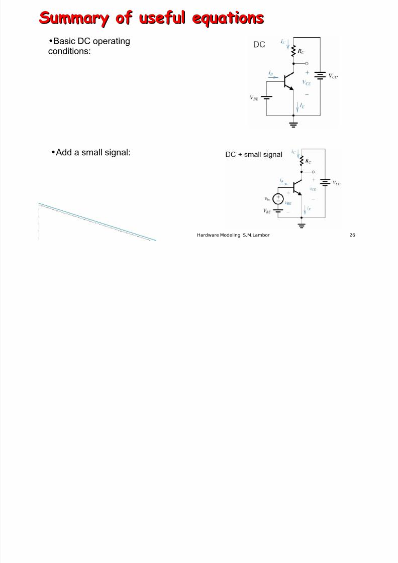
Summary of useful equationsSummary of useful equations
•Basic DC operatingconditions:
•Add a small signal:
8/7/2019 Lecture 2 Transistor Modeling
http://slidepdf.com/reader/full/lecture-2-transistor-modeling 27/44
Hardware Modeling S.M.Lambor 27
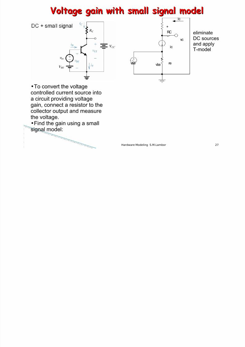
Voltage gain with small signal modelVoltage gain with small signal model
•To convert the voltagecontrolled current source intoa circuit providing voltage
gain, connect a resistor to thecollector output and measurethe voltage.•Find the gain using a smallsignal model:
vbe vbe
+
-
+
-
ic
re
RC
ic
vc
eliminateDC sourcesand applyT-model

8/7/2019 Lecture 2 Transistor Modeling
http://slidepdf.com/reader/full/lecture-2-transistor-modeling 28/44
Hardware Modeling S.M.Lambor 28
Voltage gainVoltage gain
•So, we have a voltage-to-current amplifier (a voltage controlled current source)•To convert the voltage controlled currentsource into a circuit providing voltage gain,connect a resistor to the collector output andmeasure the voltage.
So, small signal voltage gain:

8/7/2019 Lecture 2 Transistor Modeling
http://slidepdf.com/reader/full/lecture-2-transistor-modeling 29/44
Hardware Modeling S.M.Lambor 29
How to build a Common emitterHow to build a Common emitter
amplifieramplifier
•Why bother with 2 voltagesupplies?
•Use a voltage divider R2/R1 to
provide base-emitter voltage to
correctly bias the transistor.
8/7/2019 Lecture 2 Transistor Modeling
http://slidepdf.com/reader/full/lecture-2-transistor-modeling 30/44
Hardware Modeling S.M.Lambor 30
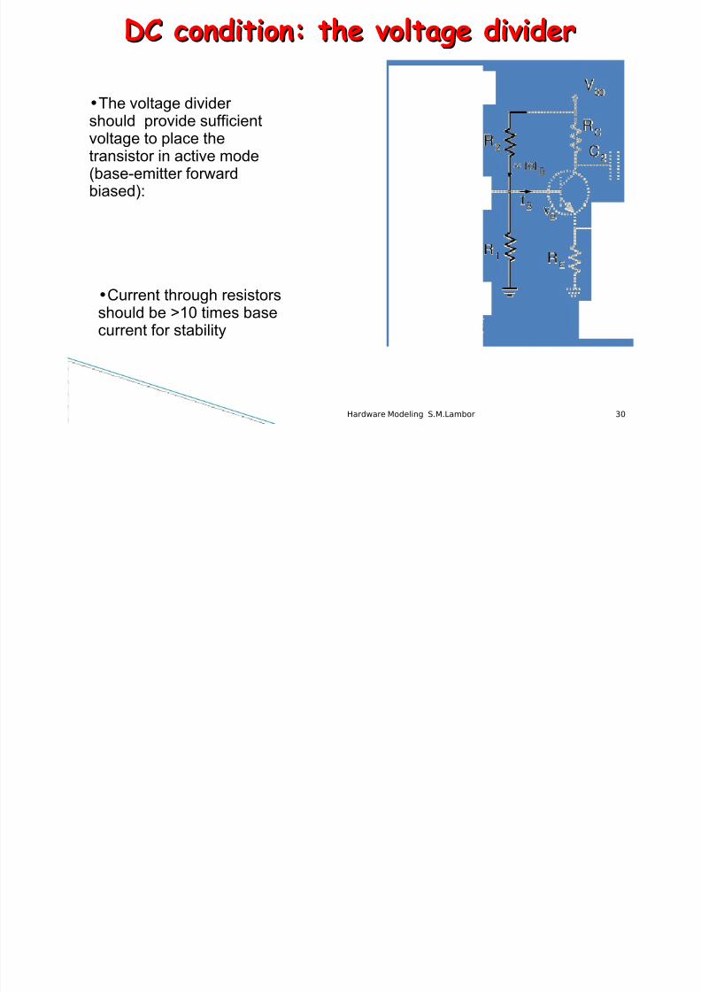
DC condition: the voltage dividerDC condition: the voltage divider
•The voltage divider should provide sufficientvoltage to place thetransistor in active mode(base-emitter forwardbiased):
•Current through resistorsshould be >10 times basecurrent for stability

8/7/2019 Lecture 2 Transistor Modeling
http://slidepdf.com/reader/full/lecture-2-transistor-modeling 31/44
Hardware Modeling S.M.Lambor 31
Amplifier specificationsAmplifier specifications
What other parameters of an amplifier do wecare about?
Voltage gain Dynamic range Frequency response (bandwidth) Input impedance Output impedance
8/7/2019 Lecture 2 Transistor Modeling
http://slidepdf.com/reader/full/lecture-2-transistor-modeling 32/44
Hardware Modeling S.M.Lambor 32
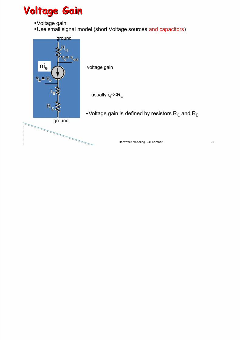
Voltage GainVoltage Gain•Voltage gain•Use small signal model (short Voltage sources and capacitors)
voltage gain
usually r e<<RE
•Voltage gain is defined by resistors RC and RE
ground
ground
αie

8/7/2019 Lecture 2 Transistor Modeling
http://slidepdf.com/reader/full/lecture-2-transistor-modeling 33/44
Hardware Modeling S.M.Lambor 33
Frequency response (Bandwidth)Frequency response (Bandwidth)
•Normally interested in providing a
small, AC signal to the base•Use capacitors to remove ("block")any low frequency (DC) component("capacitively couple the signal to thebase") which could affect the biascondition
•C1 forms a high-pass filter with R1in
parallel with R2 (Assuming the AC
impedance into the base is large).
•Cut off frequency ω0=1/RC, so to
remove frequencies <f min :

8/7/2019 Lecture 2 Transistor Modeling
http://slidepdf.com/reader/full/lecture-2-transistor-modeling 34/44
Hardware Modeling S.M.Lambor 34
Frequency response (Bandwidth)Frequency response (Bandwidth)
•Also worthwhile to place a capacitor
on the output
•C2 forms a high pass filter with RL.
•Cut off frequency ω0=1/RC, so to
remove frequencies <f min :
8/7/2019 Lecture 2 Transistor Modeling
http://slidepdf.com/reader/full/lecture-2-transistor-modeling 35/44
Hardware Modeling S.M.Lambor 35
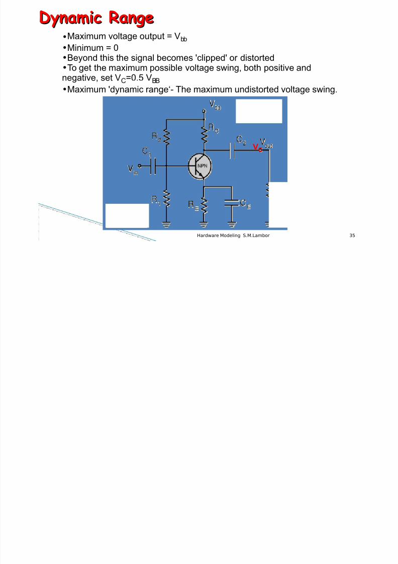
Dynamic RangeDynamic Range•Maximum voltage output = Vbb
•Minimum = 0
•Beyond this the signal becomes 'clipped' or distorted•To get the maximum possible voltage swing, both positive andnegative, set VC=0.5 VBB
•Maximum 'dynamic range‘- The maximum undistorted voltage swing.
VC

8/7/2019 Lecture 2 Transistor Modeling
http://slidepdf.com/reader/full/lecture-2-transistor-modeling 36/44
36
Input impedanceInput impedance
r b
r OUT
•Consider the circuit without the voltage
divider resistors. What's the small signal (AC)
input impedance at the base, r b?
•
•
•
•
•
•
•
•
•Including voltage divider resistors in parallel
• Input signal sees a total input
impedance r IN= R1 // R2 // r b
d

8/7/2019 Lecture 2 Transistor Modeling
http://slidepdf.com/reader/full/lecture-2-transistor-modeling 37/44
Hardware Modeling S.M.Lambor 37
Output impedanceOutput impedance
r b
ROUT
•If R L=10kΩ and we want a low frequency cutoff of 20Hz, What is C2?

8/7/2019 Lecture 2 Transistor Modeling
http://slidepdf.com/reader/full/lecture-2-transistor-modeling 38/44
Hardware Modeling S.M.Lambor 38
L q y , 2
•If VBB=15V and IC=2mA what is R C?
DC condition
Frequency response
Impedance
Gain/Dynamic range
I d

8/7/2019 Lecture 2 Transistor Modeling
http://slidepdf.com/reader/full/lecture-2-transistor-modeling 39/44
Hardware Modeling S.M.Lambor 39
ImpedancesImpedances•Why do we care about the input and output impedance?
•Simplest "black box" amplifier model:
RIN
ROUT
VIN AVIN VOUT
•The amplifier measures voltage across RIN, then generates a
voltage which is larger by a factor A
•This voltage generator, in series with the output resistance ROUT , is
connected to the output port.
•A should be a constant (i.e. gain is linear)
dI d

8/7/2019 Lecture 2 Transistor Modeling
http://slidepdf.com/reader/full/lecture-2-transistor-modeling 40/44
Hardware Modeling S.M.Lambor 40
ImpedancesImpedances•Attach an input - a source voltage VS plus source impedance RS
RIN
ROUT
VINAVIN
VOUT
•Note the voltage divider RS + RIN.
•VIN=VS(RIN/(RIN+RS)
•We want VIN = VS regardless of source impedance
•So want RIN to be large.
•The ideal amplifier has an infinite input impedance
VS
RS
dI d

8/7/2019 Lecture 2 Transistor Modeling
http://slidepdf.com/reader/full/lecture-2-transistor-modeling 41/44
Hardware Modeling S.M.Lambor 41
ImpedancesImpedances•Attach a load - an output circuit with a resistance RL
•Note the voltage divider ROUT + RL.
•VOUT =AVIN(RL/(RL+ROUT )
•Want VOUT =AVIN regardless of load
•We want ROUT to be small.
•The ideal amplifier has zero output impedance
RIN
ROUT
VINAVIN VOUT
VS
RS
RL
8/7/2019 Lecture 2 Transistor Modeling
http://slidepdf.com/reader/full/lecture-2-transistor-modeling 42/44
Hardware Modeling S.M.Lambor 42
Capacitor Selection for the CE Amplifier
The key objective in design is to make the capacitive reactancemuch smaller at the operating frequency f than the associated
resistance that must be coupled or bypassed.

8/7/2019 Lecture 2 Transistor Modeling
http://slidepdf.com/reader/full/lecture-2-transistor-modeling 43/44
Hardware Modeling S.M.Lambor 43
Static power dissipation in amplifiers isdetermined from their DC equivalentcircuits.
Amplifier Power DissipationAmplifier Power Dissipation
Total power dissipated in C-Band E-B junctions is:
where
Total power supplied is:
The difference is the power dissipated by the bias resistors.
8/7/2019 Lecture 2 Transistor Modeling
http://slidepdf.com/reader/full/lecture-2-transistor-modeling 44/44
Questions
? ? ?? ? ? ?
? ? ?