Introduction to FPGA -...
36
ACCESS IC LAB Graduate Institute of Electronics Engineering, NTU Introduction to FPGA Presenter: CMH Advisor: Prof. An-Yeu Wu 2010/11/23
Transcript of Introduction to FPGA -...
ACCESS IC LAB
Graduate Institute of Electronics Engineering, NTU
Introduction to FPGA
Presenter: CMH
Advisor: Prof. An-Yeu Wu
2010/11/23
ACCESS IC LAB Graduate Institute of Electronics Engineering, NTU
pp. 2
Outline
Basic Concepts of FPGA
Architecture and Feature of Xilinx FPGA
Reference
ACCESS IC LAB
Graduate Institute of Electronics Engineering, NTU
Basic Concepts of FPGA
ACCESS IC LAB Graduate Institute of Electronics Engineering, NTU
pp. 4
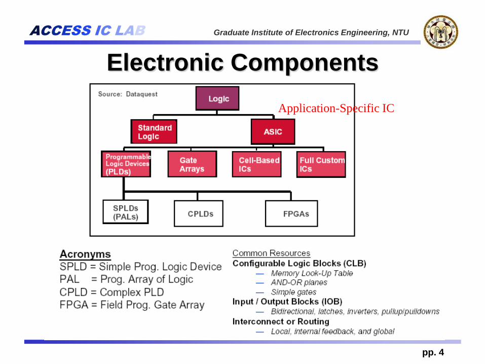
Electronic Components
Application-Specific IC
ACCESS IC LAB Graduate Institute of Electronics Engineering, NTU
pp. 5
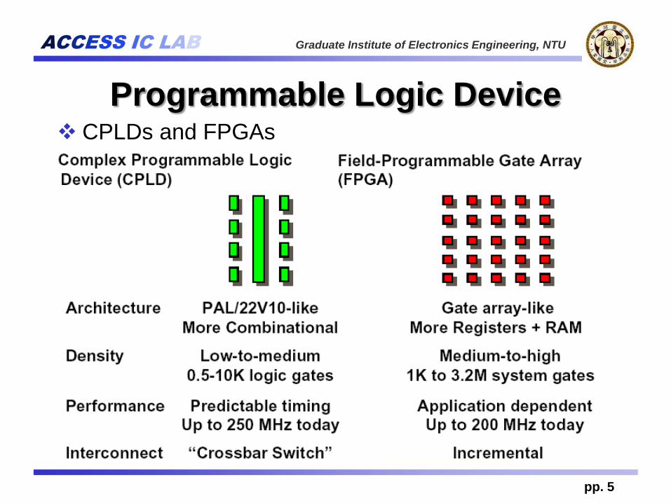
Programmable Logic Device CPLDs and FPGAs
ACCESS IC LAB Graduate Institute of Electronics Engineering, NTU
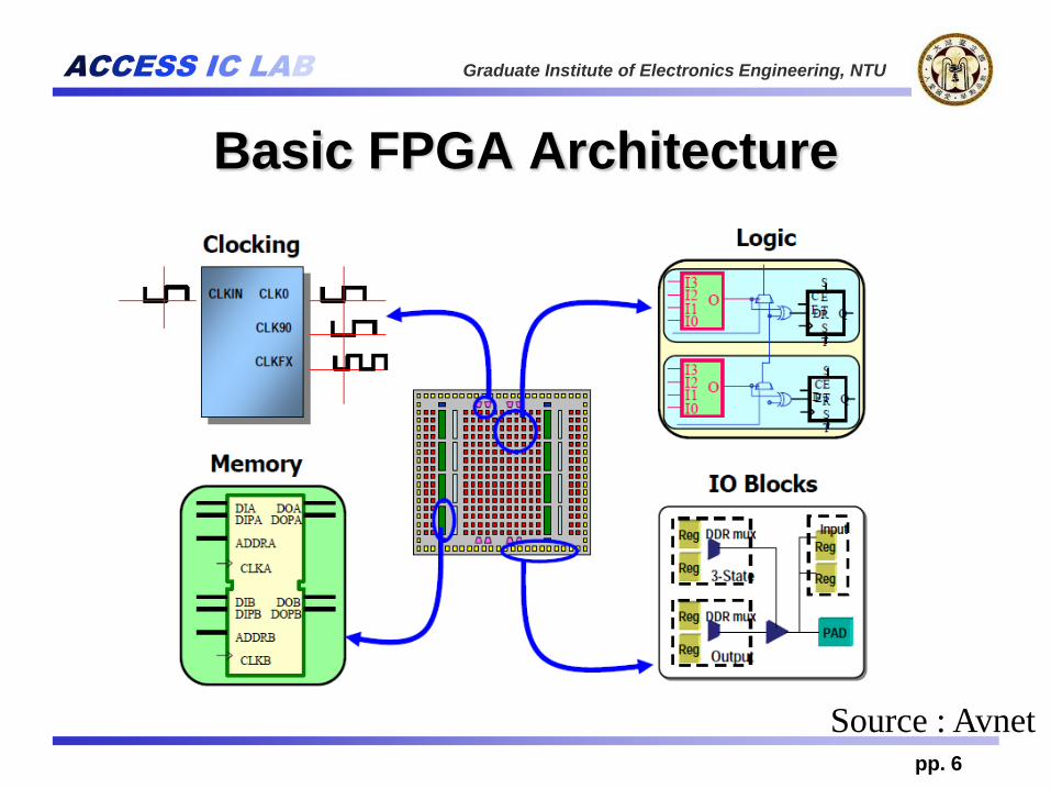
Basic FPGA Architecture
pp. 6
Source : Avnet
ACCESS IC LAB Graduate Institute of Electronics Engineering, NTU
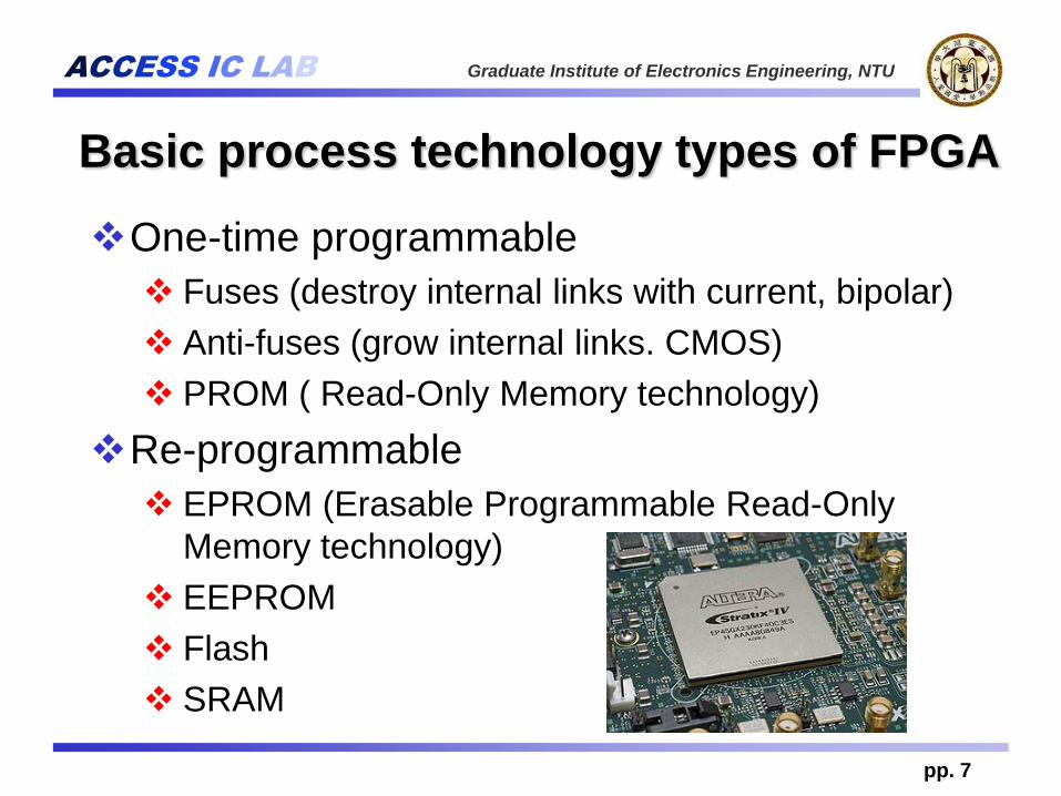
Basic process technology types of FPGA
pp. 7
One-time programmable
Fuses (destroy internal links with current, bipolar)
Anti-fuses (grow internal links. CMOS)
PROM ( Read-Only Memory technology)
Re-programmable
EPROM (Erasable Programmable Read-Only
Memory technology)
EEPROM
Flash
SRAM
ACCESS IC LAB Graduate Institute of Electronics Engineering, NTU
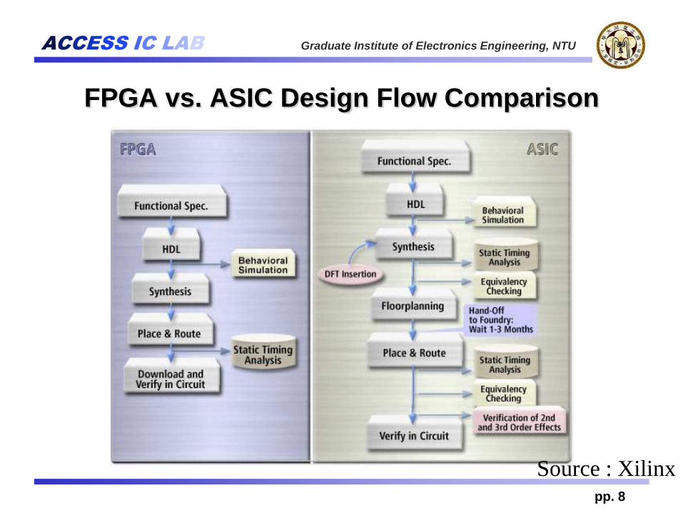
FPGA vs. ASIC Design Flow Comparison
pp. 8
Source : Xilinx
ACCESS IC LAB Graduate Institute of Electronics Engineering, NTU
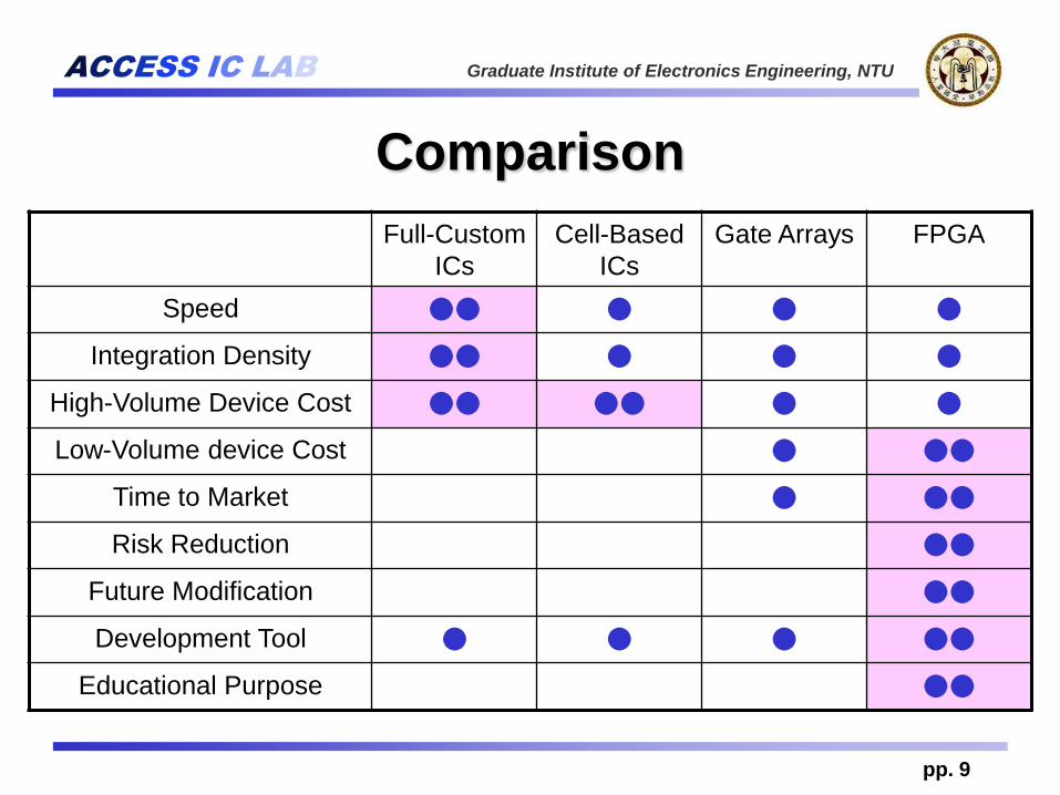
pp. 9
Comparison
Full-Custom
ICs
Cell-Based
ICs
Gate Arrays FPGA
Speed ●● ● ● ●
Integration Density ●● ● ● ●
High-Volume Device Cost ●● ●● ● ●
Low-Volume device Cost ● ●●
Time to Market ● ●●
Risk Reduction ●●
Future Modification ●●
Development Tool ● ● ● ●●
Educational Purpose ●●
ACCESS IC LAB Graduate Institute of Electronics Engineering, NTU
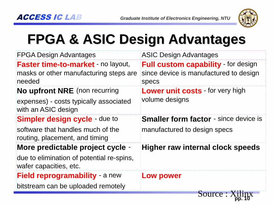
FPGA & ASIC Design Advantages
pp. 10
FPGA Design Advantages ASIC Design Advantages
Faster time-to-market - no layout,
masks or other manufacturing steps are
needed
Full custom capability - for design
since device is manufactured to design
specs
No upfront NRE (non recurring
expenses) - costs typically associated
with an ASIC design
Lower unit costs - for very high
volume designs
Simpler design cycle - due to
software that handles much of the
routing, placement, and timing
Smaller form factor - since device is
manufactured to design specs
More predictable project cycle -
due to elimination of potential re-spins,
wafer capacities, etc.
Higher raw internal clock speeds
Field reprogramability - a new
bitstream can be uploaded remotely
Low power
Source : Xilinx
ACCESS IC LAB Graduate Institute of Electronics Engineering, NTU
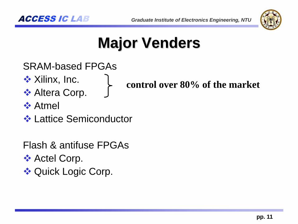
Major Venders
pp. 11
SRAM-based FPGAs
Xilinx, Inc.
Altera Corp.
Atmel
Lattice Semiconductor
Flash & antifuse FPGAs
Actel Corp.
Quick Logic Corp.
control over 80% of the market
ACCESS IC LAB Graduate Institute of Electronics Engineering, NTU
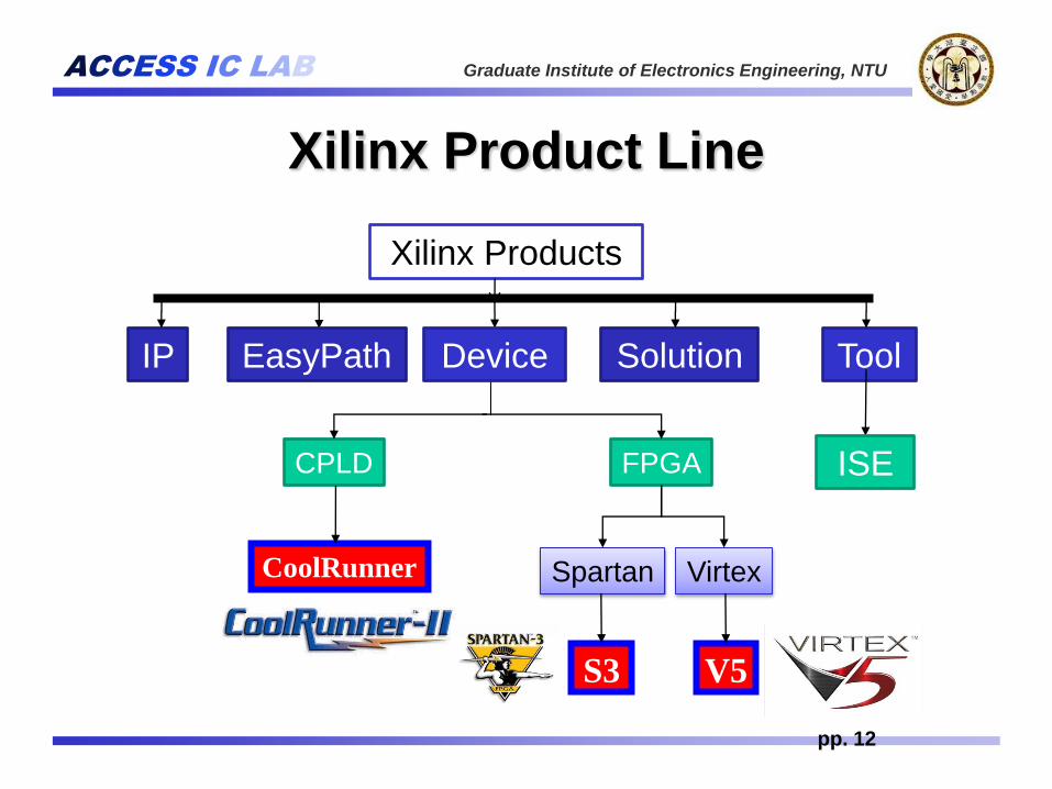
Xilinx Product Line
pp. 12
ToolIP
Xilinx Products
SolutionEasyPath
ISE
Device
CPLD FPGA
Spartan VirtexCoolRunner
S3 V5
ACCESS IC LAB Graduate Institute of Electronics Engineering, NTU
pp. 13
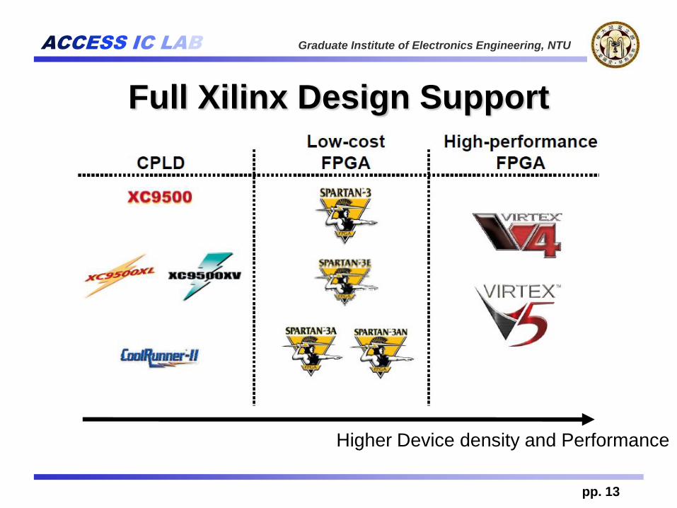
Full Xilinx Design Support
Higher Device density and Performance
ACCESS IC LAB
Graduate Institute of Electronics Engineering, NTU
Architecture and Feature of
Xilinx FPGA
ACCESS IC LAB Graduate Institute of Electronics Engineering, NTU
Overview
pp. 15
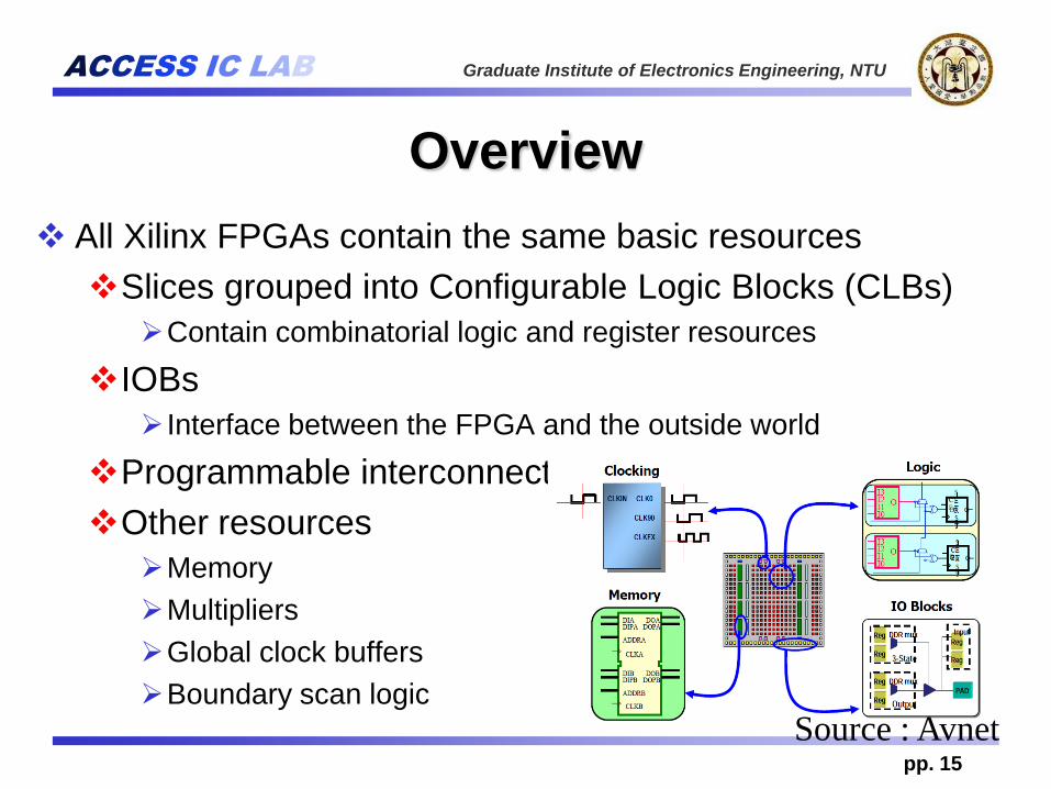
All Xilinx FPGAs contain the same basic resources
Slices grouped into Configurable Logic Blocks (CLBs)
Contain combinatorial logic and register resources
IOBs
Interface between the FPGA and the outside world
Programmable interconnect
Other resources
Memory
Multipliers
Global clock buffers
Boundary scan logic
Source : Avnet
ACCESS IC LAB Graduate Institute of Electronics Engineering, NTU
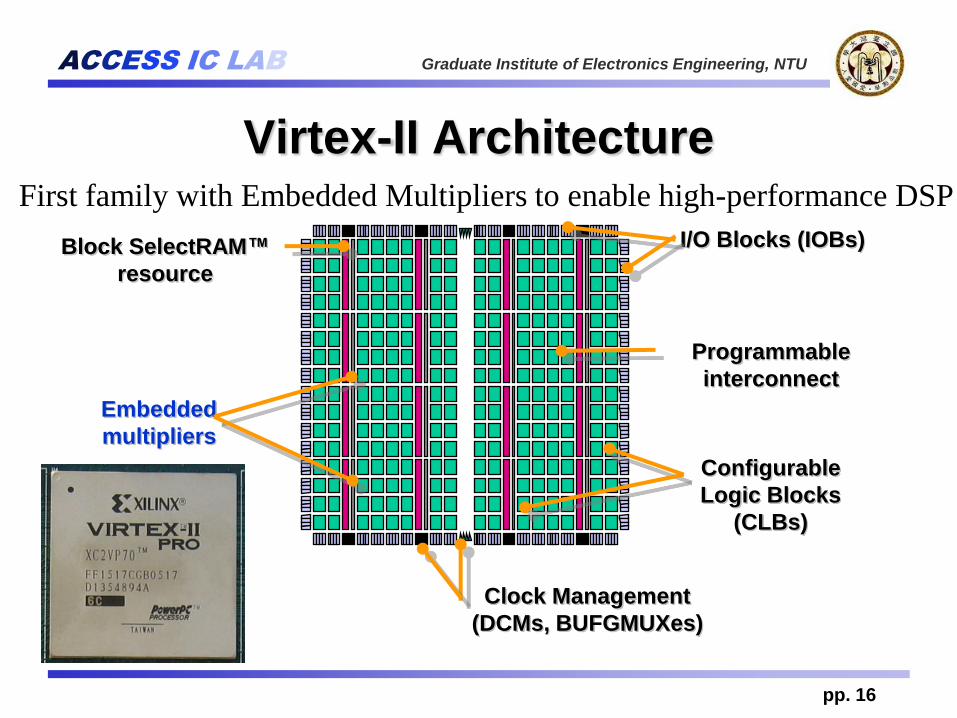
Virtex-II Architecture
pp. 16
I/O Blocks (IOBs)
Configurable
Logic Blocks
(CLBs)
Clock Management
(DCMs, BUFGMUXes)
Block SelectRAM™
resource
Embedded
multipliers
Programmable
interconnect
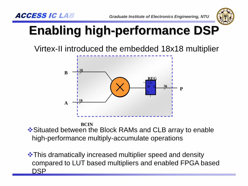
First family with Embedded Multipliers to enable high-performance DSP
ACCESS IC LAB Graduate Institute of Electronics Engineering, NTU
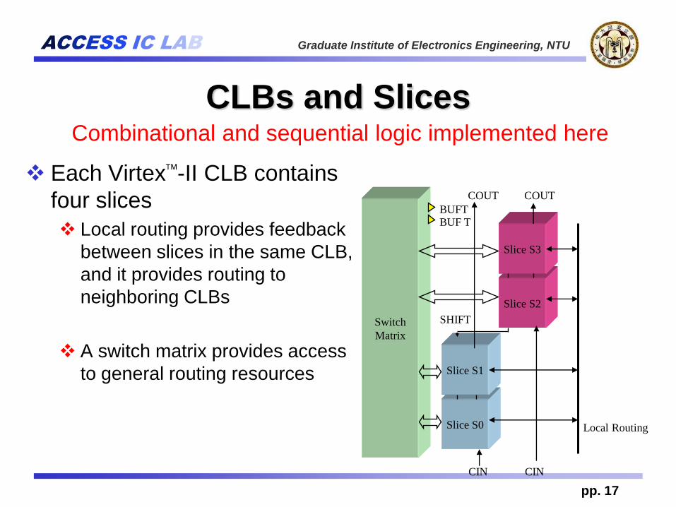
CLBs and Slices
pp. 17
Each Virtex-II CLB contains
four slices
Local routing provides feedback
between slices in the same CLB,
and it provides routing to
neighboring CLBs
A switch matrix provides access
to general routing resources
CIN
Switch
Matrix
BUFTBUF T
COUTCOUT
Slice S0
Slice S1
Local Routing
Slice S2
Slice S3
CIN
SHIFT
Combinational and sequential logic implemented here
ACCESS IC LAB Graduate Institute of Electronics Engineering, NTU
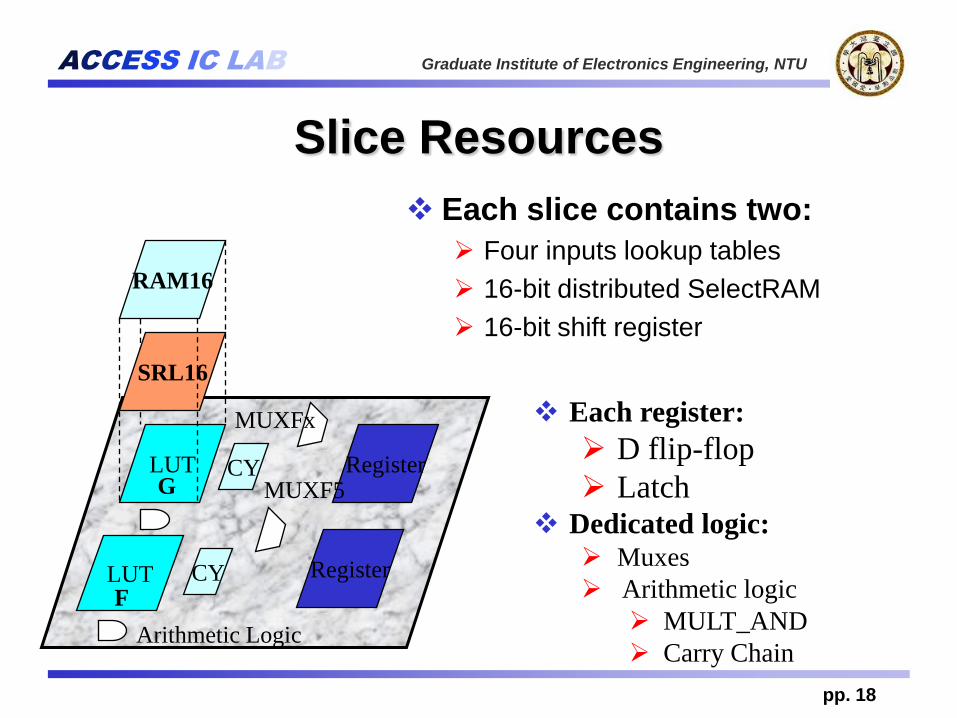
Slice Resources
pp. 18
Each slice contains two:
Four inputs lookup tables
16-bit distributed SelectRAM
16-bit shift register
Each register:
D flip-flop
Latch Dedicated logic: Muxes
Arithmetic logic
MULT_AND
Carry Chain
LUT
Register
Register
LUT CY
CY
SRL16
RAM16
G
F
MUXF5
Arithmetic Logic
MUXFx
ACCESS IC LAB Graduate Institute of Electronics Engineering, NTU
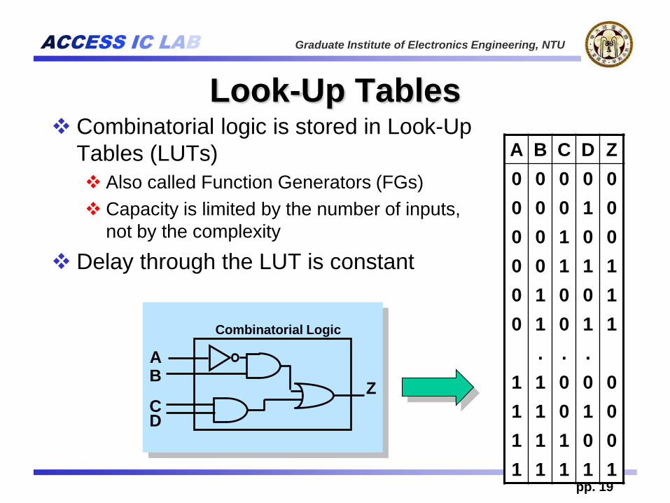
Look-Up Tables
pp. 19
Combinatorial Logic
AB
CD
Z
Combinatorial logic is stored in Look-Up
Tables (LUTs)
Also called Function Generators (FGs)
Capacity is limited by the number of inputs,
not by the complexity
Delay through the LUT is constant
A B C D Z
0 0 0 0 0
0 0 0 1 0
0 0 1 0 0
0 0 1 1 1
0 1 0 0 1
0 1 0 1 1
. . .
1 1 0 0 0
1 1 0 1 0
1 1 1 0 0
1 1 1 1 1
ACCESS IC LAB Graduate Institute of Electronics Engineering, NTU
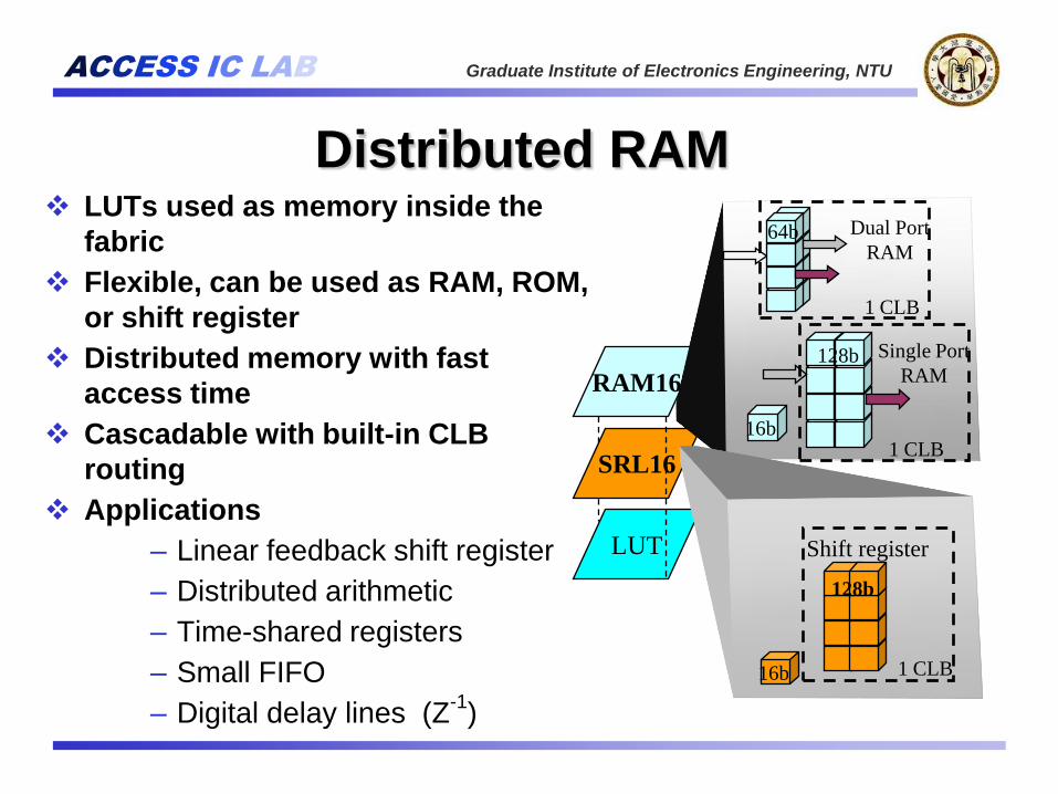
LUTs used as memory inside the
fabric
Flexible, can be used as RAM, ROM,
or shift register
Distributed memory with fast
access time
Cascadable with built-in CLB
routing
Applications
– Linear feedback shift register
– Distributed arithmetic
– Time-shared registers
– Small FIFO
– Digital delay lines (Z-1
)
Distributed RAM
LUT
SRL16
RAM16
16b
128b
1 CLB
Single Port
RAM
64b64b
1 CLB
Dual Port
RAM
16b
Shift register
1 CLB
128b
ACCESS IC LAB Graduate Institute of Electronics Engineering, NTU
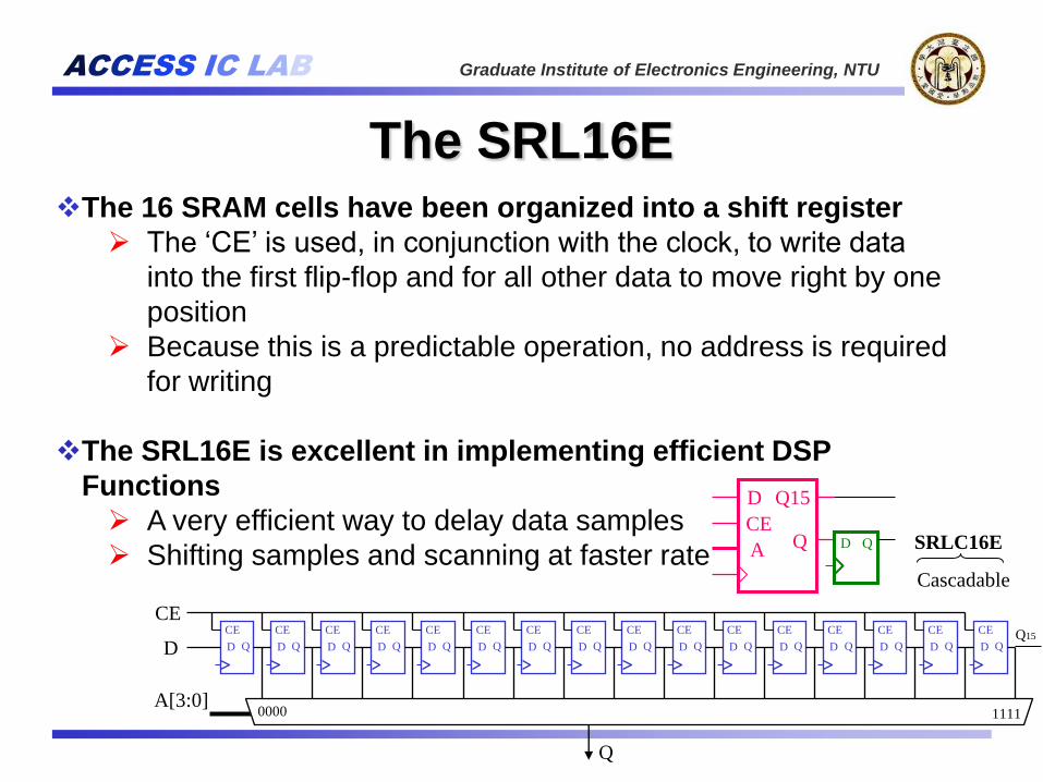
The SRL16E The 16 SRAM cells have been organized into a shift register
The „CE‟ is used, in conjunction with the clock, to write data
into the first flip-flop and for all other data to move right by one
position
Because this is a predictable operation, no address is required
for writing
The SRL16E is excellent in implementing efficient DSP
Functions
A very efficient way to delay data samples
Shifting samples and scanning at faster rate A QCE
D Q
D Q15
SRLC16E
Cascadable
D
CECE
QD
CE
QD
CE
QD
CE
QD
CE
QD
CE
QD
CE
QD
CE
QD
CE
QD
CE
QD
CE
QD
CE
QD
CE
QD
CE
QD
CE
QD
CE
QD
A[3:0]0000 1111
Q
Q15
ACCESS IC LAB Graduate Institute of Electronics Engineering, NTU
pp. 22
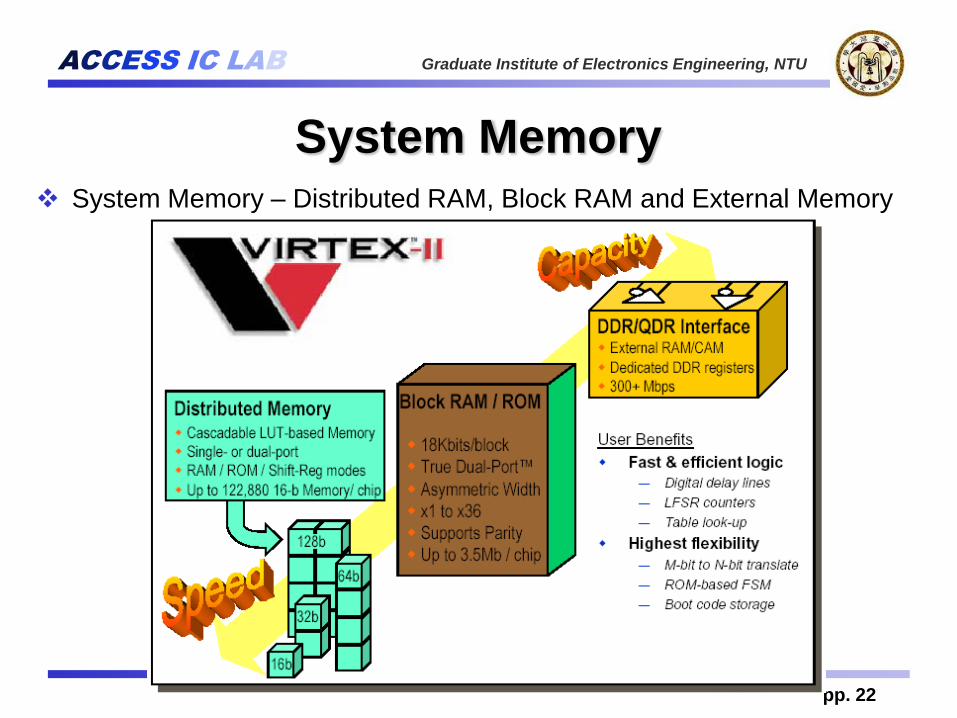
System Memory – Distributed RAM, Block RAM and External Memory
System Memory
ACCESS IC LAB Graduate Institute of Electronics Engineering, NTU
pp. 23
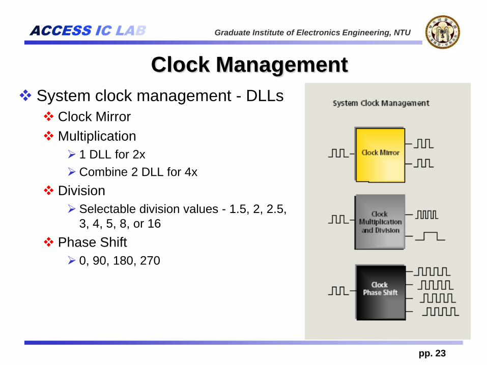
Clock Management
System clock management - DLLs
Clock Mirror
Multiplication
1 DLL for 2x
Combine 2 DLL for 4x
Division
Selectable division values - 1.5, 2, 2.5,
3, 4, 5, 8, or 16
Phase Shift
0, 90, 180, 270
ACCESS IC LAB Graduate Institute of Electronics Engineering, NTU
pp. 24
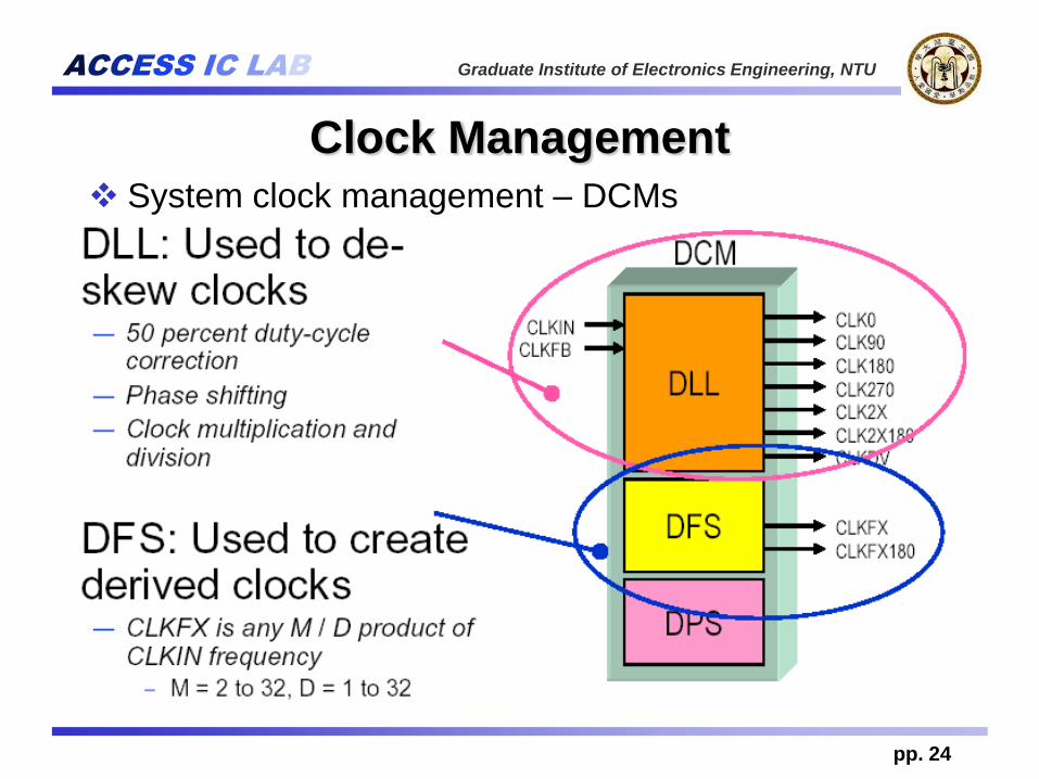
Clock Management
System clock management – DCMs
ACCESS IC LAB Graduate Institute of Electronics Engineering, NTU
pp. 25
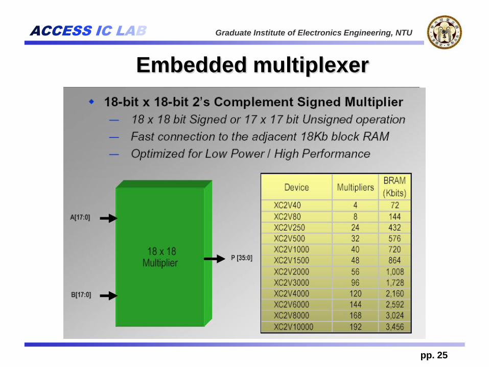
Embedded multiplexer
ACCESS IC LAB Graduate Institute of Electronics Engineering, NTU
Enabling high-performance DSP
Situated between the Block RAMs and CLB array to enable
high-performance multiply-accumulate operations
This dramatically increased multiplier speed and density
compared to LUT based multipliers and enabled FPGA based
DSP
P
CE
REG
D Q
A
BCIN
B18
36
18
Virtex-II introduced the embedded 18x18 multiplier
ACCESS IC LAB Graduate Institute of Electronics Engineering, NTU
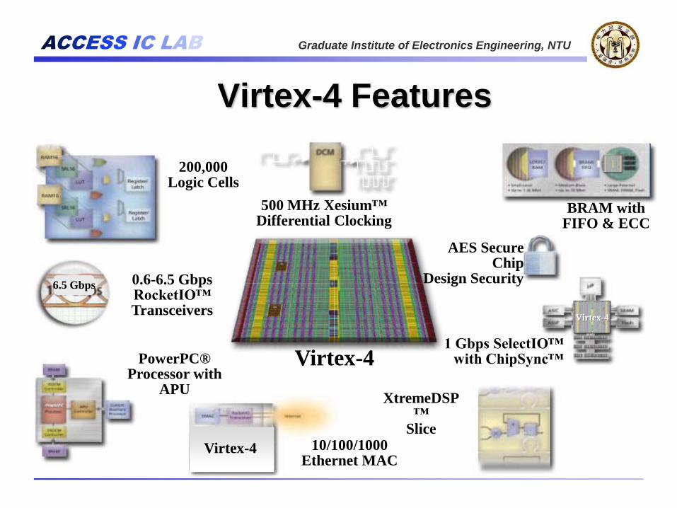
Virtex-4
Virtex-4
Virtex-4 Features
200,000Logic Cells
0.6-6.5 Gbps RocketIO™ Transceivers
PowerPC® Processor with
APU
10/100/1000 Ethernet MAC
XtremeDSP™
Slice
1 Gbps SelectIO™ with ChipSync™
AES Secure Chip
Design Security
BRAM with FIFO & ECC
500 MHz Xesium™Differential Clocking
6.5 Gbps
Virtex-4
ACCESS IC LAB Graduate Institute of Electronics Engineering, NTU
pp. 28
ACCESS IC LAB Graduate Institute of Electronics Engineering, NTU
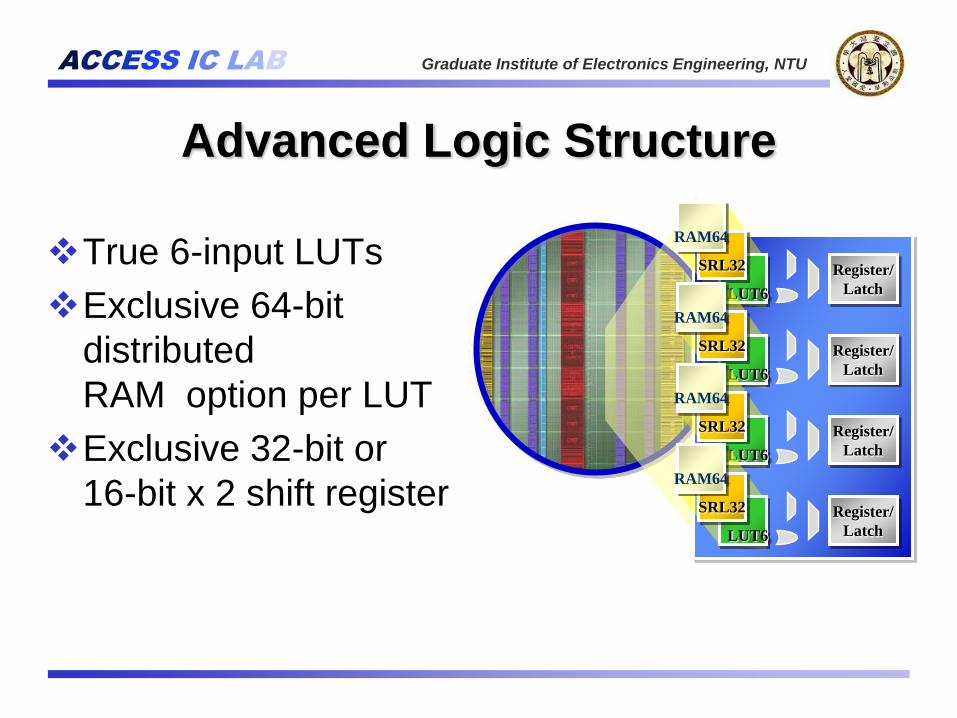
Advanced Logic Structure
True 6-input LUTs
Exclusive 64-bit
distributed
RAM option per LUT
Exclusive 32-bit or
16-bit x 2 shift register
LUT6
SRL32
RAM64
LUT6
SRL32
RAM64
LUT6
SRL32
RAM64
LUT6
SRL32
RAM64
Register/
Latch
Register/
Latch
Register/
Latch
Register/
Latch
ACCESS IC LAB Graduate Institute of Electronics Engineering, NTU
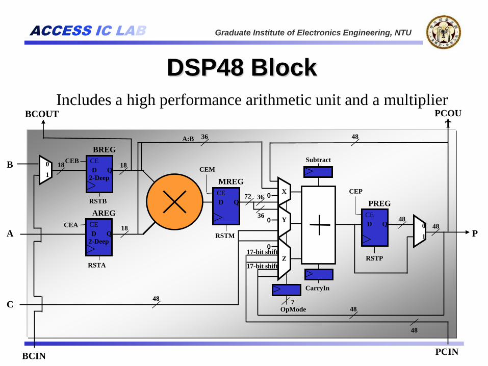
DSP48 Block
4848
48
Subtract
P
RSTA
18
PCIN
0
PCOU
T
C
BCOUT
BCIN
B
CarryIn
0
072
RSTM
A:B 36
Y
Z
OpMode7
18
48
48
17-bit shift
17-bit shift
48
1
0
0
1
36
36
18
X
CEM
CE
MREG
D Q
RSTP
CEP
CE
PREG
D Q
CEB CE
BREG
D Q
CEA CE
AREG
D Q
RSTB
A
2-Deep
2-Deep
Includes a high performance arithmetic unit and a multiplier
ACCESS IC LAB Graduate Institute of Electronics Engineering, NTU
DSP48 Block
Enables time-division
multiplexing for DSP
Over 40 different modes
Each XtremeDSP Slice
individually controllable
Change operation in a
single clock cycle
Control functionality from
logic, memory or processor
6 5 4 3 2 1 0
Zero 0 0 0 0 0 0 0 +/- Cin
Hold P 0 0 0 0 0 1 0 +/- (P + Cin)
A:B Select 0 0 0 0 0 1 1 +/- (A:B + Cin)
Multiply 0 0 0 0 1 0 1 +/- (A * B + Cin)
C Select 0 0 0 1 1 0 0 +/- (C + Cin)
Feedback Add 0 0 0 1 1 1 0 +/- (C + P + Cin)
36-Bit Adder 0 0 0 1 1 1 1 +/- (A:B + C + Cin)
P Cascade Select 0 0 1 0 0 0 0 PCIN +/- Cin
P Cascade Feedback Add 0 0 1 0 0 1 0 PCIN +/- (P + Cin)
P Cascade Add 0 0 1 0 0 1 1 PCIN +/- (A:B + Cin)
P Cascade Multiply Add 0 0 1 0 1 0 1 PCIN +/- (A * B + Cin)
P Cascade Add 0 0 1 1 1 0 0 PCIN +/- (C + Cin)
P Cascade Feedback Add Add0 0 1 1 1 1 0 PCIN +/- (C + P + Cin)
P Cascade Add Add 0 0 1 1 1 1 1 PCIN +/- (A:B + C + Cin)
Hold P 0 1 0 0 0 0 0 P +/- Cin
Double Feedback Add 0 1 0 0 0 1 0 P +/- (P + Cin)
Feedback Add 0 1 0 0 0 1 1 P +/- (A:B + Cin)
Multiply-Accumulate 0 1 0 0 1 0 1 P +/- (A * B + Cin)
Feedback Add 0 1 0 1 1 0 0 P +/- (C + Cin)
Double Feedback Add 0 1 0 1 1 1 0 P +/- (C + P + Cin)
Feedback Add Add 0 1 0 1 1 1 1 P +/- (A:B + C + Cin)
C Select 0 1 1 0 0 0 0 C +/- Cin
Feedback Add 0 1 1 0 0 1 0 C +/- (P + Cin)
36-Bit Adder 0 1 1 0 0 1 1 C +/- (A:B + Cin)
Multiply-Add 0 1 1 0 1 0 1 C +/- (A * B + Cin)
Double 0 1 1 1 1 0 0 C +/- (C + Cin)
Double Add Feedback Add 0 1 1 1 1 1 0 C +/- (C + P + Cin)
Double Add 0 1 1 1 1 1 1 C +/- (A:B + C + Cin)
OpMode OutputXYZ
Dynamically Programmable DSP Op Modes
ACCESS IC LAB Graduate Institute of Electronics Engineering, NTU
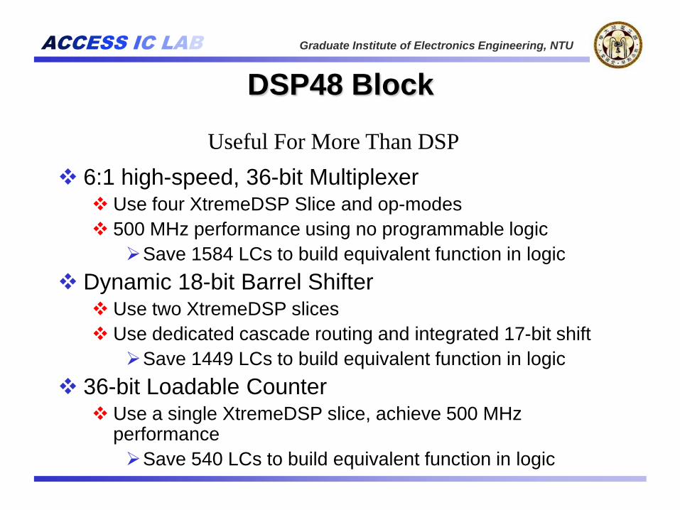
DSP48 Block
6:1 high-speed, 36-bit Multiplexer Use four XtremeDSP Slice and op-modes
500 MHz performance using no programmable logic
Save 1584 LCs to build equivalent function in logic
Dynamic 18-bit Barrel Shifter Use two XtremeDSP slices
Use dedicated cascade routing and integrated 17-bit shift
Save 1449 LCs to build equivalent function in logic
36-bit Loadable Counter Use a single XtremeDSP slice, achieve 500 MHz
performance
Save 540 LCs to build equivalent function in logic
Useful For More Than DSP
ACCESS IC LAB Graduate Institute of Electronics Engineering, NTU
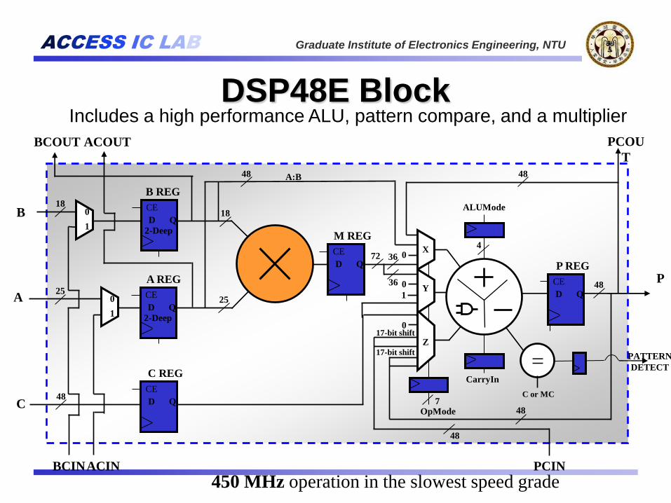
DSP48E Block
450 MHz operation in the slowest speed grade
36
OpMode7
48A:B48
0
072
Y36
X
017-bit shift
17-bit shift
P
B
PCIN
PCOU
T
48
25
18
CE
M REG
D Q
CE
P REG
D QA
18
ACOUT
BCIN
0
1
48
C
ALUMode
CarryIn
48
Z
CE
C REG
D Q
BCOUT
ACIN
0
1
1
4
= PATTERN
DETECT
C or MC
25
48
CE
A REG
D Q
2-Deep
CE
B REG
D
2-Deep
Q
Includes a high performance ALU, pattern compare, and a multiplier
ACCESS IC LAB Graduate Institute of Electronics Engineering, NTU
DSP48E
Virtex-5SX introduced a few new improvements in the DSP48E “enhanced” DSP block
The adder block was modified to become a mulifunctional ALU. A pattern compare was added to support the detection of saturation, overflow and underflow conditions
A 48-bit carry chain supports the propagation of partial sum and product carry‟s so multiple DSP48E blocks can be chained to give higher bit precision
ALU opcodes are dynamically controlled allowing functional changes on a clock cycle basis
ACCESS IC LAB Graduate Institute of Electronics Engineering, NTU
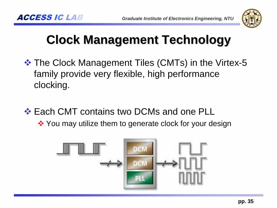
Clock Management Technology
The Clock Management Tiles (CMTs) in the Virtex-5
family provide very flexible, high performance
clocking.
Each CMT contains two DCMs and one PLL
You may utilize them to generate clock for your design
pp. 35
ACCESS IC LAB Graduate Institute of Electronics Engineering, NTU
Reference
For more details, visit
http://www.xilinx.com/products/virtex5/index.htm
Virtex-5 FPGA User Guide
http://www.xilinx.com/support/documentation/user_guid
es/ug190.pdf
pp. 36