PolarFire FPGA
86
DS0141 Datasheet PolarFire FPGA
Transcript of PolarFire FPGA

DS0141Datasheet
PolarFire FPGA
PolarFire FPGA
Microsemi Proprietary and Confidential. DS0141 Datasheet Revision 1.1
Contents
1 Revision History ............................................................................................................................. 11.1 Revision 1.1 ........................................................................................................................................ 11.2 Revision 1.0 ........................................................................................................................................ 1
2 Overview ........................................................................................................................................ 2
3 References ..................................................................................................................................... 3
4 Device Offering .............................................................................................................................. 4
5 Silicon Status .................................................................................................................................. 5
6 DC Characteristics .......................................................................................................................... 66.1 Absolute Maximum Rating ................................................................................................................. 66.2 Recommended Operating Conditions ................................................................................................ 6
6.2.1 DC Characteristics over Recommended Operating Conditions ............................................................... 8
6.2.2 Maximum Allowed Overshoot and Undershoot ..................................................................................... 9
6.3 Input and Output .............................................................................................................................. 126.3.1 DC Input and Output Levels .................................................................................................................. 12
6.3.2 Differential DC Input and Output Levels ............................................................................................... 14
6.3.3 Complementary Differential DC Input and Output Levels .................................................................... 15
6.3.4 HSIO On-Die Termination ...................................................................................................................... 17
6.3.5 GPIO On-Die Termination ...................................................................................................................... 18
6.3.6 LVDS ...................................................................................................................................................... 19
7 AC Switching Characteristics ........................................................................................................ 217.1 I/O Standards Specifications ............................................................................................................. 21
7.1.1 Input Delay Measurement Methodology .............................................................................................. 21
7.1.2 Output Delay Measurement Methodology ........................................................................................... 24
7.1.3 Input Buffer Speed ................................................................................................................................ 26
7.1.4 Output Buffer Speed ............................................................................................................................. 28
7.1.5 Maximum PHY Rate for Memory Interface IP ....................................................................................... 30
7.1.6 User I/O Switching Characteristics ........................................................................................................ 31
7.1.7 I/O Digital Latency ................................................................................................................................. 34
7.1.8 I/O Digital Training Calibration .............................................................................................................. 37
7.2 Clocking Specifications ..................................................................................................................... 387.2.1 Clocking ................................................................................................................................................. 38
7.2.2 PLL ......................................................................................................................................................... 40
7.2.3 DLL ......................................................................................................................................................... 41
7.2.4 RC Oscillators ......................................................................................................................................... 42
7.3 Fabric Specifications ......................................................................................................................... 42
PolarFire FPGA
Microsemi Proprietary and Confidential. DS0141 Datasheet Revision 1.1
7.3.1 Math Blocks ........................................................................................................................................... 42
7.3.2 LSRAM Blocks ........................................................................................................................................ 43
7.4 Transceiver Switching Characteristics .............................................................................................. 467.4.1 Transceiver Performance ...................................................................................................................... 46
7.4.2 Transceiver Reference Clock Performance ........................................................................................... 46
7.4.3 Transceiver Reference Clock I/O Standards .......................................................................................... 47
7.4.4 Transceiver Interface Performance ....................................................................................................... 48
7.4.5 Transmitter Performance ...................................................................................................................... 48
7.4.6 Receiver Performance ........................................................................................................................... 51
7.5 Transceiver Protocol Characteristics ................................................................................................ 537.5.1 PCI Express ............................................................................................................................................ 53
7.5.2 10GbE (XAUI, RXAUI, 10GBASE-R, and 10GBASE-KR) ............................................................................ 53
7.5.3 1GbE (SGMII, 1000BASE-T, 1000BASE-X, and QSGMII) ......................................................................... 54
7.5.4 CPRI ....................................................................................................................................................... 55
7.5.5 JESD204B ............................................................................................................................................... 56
7.6 Non-Volatile Characteristics ............................................................................................................. 567.6.1 FPGA Programming Cycle and Retention .............................................................................................. 56
7.6.2 FPGA Programming Time ...................................................................................................................... 57
7.6.3 FPGA Bitstream Sizes ............................................................................................................................. 57
7.6.4 Digest Cycles .......................................................................................................................................... 57
7.6.5 Digest Time ............................................................................................................................................ 58
7.6.6 Zeroization Time .................................................................................................................................... 59
7.6.7 Verify Time ............................................................................................................................................ 61
7.6.8 Secure NVM Performance ..................................................................................................................... 62
7.6.9 Secure NVM Programming Cycles ......................................................................................................... 62
7.7 System Services ................................................................................................................................ 637.7.1 System Services Throughput Characteristics ......................................................................................... 63
7.8 User Crypto ....................................................................................................................................... 647.8.1 TeraFire 5200B Switching Characteristics ............................................................................................. 64
7.8.2 TeraFire 5200B Throughput Characteristics .......................................................................................... 64
7.9 Fabric Macros ................................................................................................................................... 687.9.1 UJTAG Switching Characteristics ........................................................................................................... 68
7.9.2 UJTAG_SEC Switching Characteristics ................................................................................................... 68
7.9.3 USPI Switching Characteristics .............................................................................................................. 69
7.9.4 Tamper Detectors .................................................................................................................................. 69
7.9.5 System Controller Suspend Switching Characteristics .......................................................................... 72
7.9.6 Dynamic Reconfiguration Interface ....................................................................................................... 72
7.10 Power-Up to Functional Timing ...................................................................................................... 747.10.1 LSRAM and μSRAM Initialization Time ................................................................................................ 78
7.11 Dedicated Pins ................................................................................................................................ 787.11.1 JTAG Switching Characteristics ............................................................................................................ 78
PolarFire FPGA
Microsemi Proprietary and Confidential. DS0141 Datasheet Revision 1.1
7.11.2 SPI Switching Characteristics ............................................................................................................... 79
7.11.3 SmartDebug Probe Switching Characteristics ..................................................................................... 80
7.11.4 DEVRST_N Switching Characteristics ................................................................................................... 80
7.11.5 FF_EXIT Switching Characteristics ....................................................................................................... 80
7.11.6 IO_CFG Switching Characteristics ........................................................................................................ 80
PolarFire FPGA
Microsemi Proprietary and Confidential. DS0141 Datasheet Revision 1.1 1
1 Revision HistoryThe revision history describes the changes that were implemented in the document. The changes are listed by revision, starting with the most current publication.
1.1 Revision 1.1Revision 1.1 was published in August 2017. The following is a summary of changes.
LVDS specifications changed to 1.25G. For more information, see HSIO Maximum Input Buffer Speed and .(see page 26) HSIO Maximum Output Buffer Speed (see page 28)
LVDS18, LVDS25/LVDS33, and LVDS25 specifications changed to 800 Mbps. For more information, see .I/O Standards Specifications (see page 21)A note was added indicting a zeroization cycle counts as a programming cycle. For more information, see .Non-Volatile Characteristics (see page 56)A note was added defining power down conditions for programming recovery conditions. For more information, see .Power-Supply Ramp Times (see page 11)
1.2 Revision 1.0Revision 1.0 was the first publication of this document.
PolarFire FPGA
Microsemi Proprietary and Confidential. DS0141 Datasheet Revision 1.1 2
2 OverviewThis datasheet describes PolarFire™ FPGA device characteristics with industrial temperature range(–40 °C to 100 °C T ) and extended commercial temperature range (0 °C to 100 °C T ). The devices are J J
provided with a standard speed grade (STD) and a –1 speed grade with higher performance. The FPGA core supply V can operate at 1.0 V for lower-power or 1.05 V for higher performance. Similarly, the DD
transceiver core supply V can also operate at 1.0 V or 1.05 V. Users select the core operating voltage DDA
while creating the project.
PolarFire FPGA
Microsemi Proprietary and Confidential. DS0141 Datasheet Revision 1.1 3
3 ReferencesThe following documents are recommended references. For more information about PolarFire static and dynamic power data, see the .PolarFire Power Estimator Spreadsheet
PO0137: PolarFire FPGA Product OverviewUG0722: PolarFire FPGA Packaging and Pin Descriptions Users GuideUG0726: PolarFire FPGA Board Design User GuideUG0686: PolarFire FPGA User I/O User GuideUG0680: PolarFire FPGA Fabric User GuideUG0714: PolarFire FPGA Programming User GuideUG0684: PolarFire FPGA Clocking Resources User GuideUG0687: PolarFire FPGA 1G Ethernet Solutions User GuideUG0727: PolarFire FPGA 10G Ethernet Solutions User GuideUG0748: PolarFire FPGA Low Power User GuideUG0676: PolarFire FPGA DDR Memory Controller User GuideUG0743: PolarFire FPGA Debugging User GuideUG0725: PolarFire FPGA Device Power-Up and Resets User GuideUG0677: PolarFire FPGA Transceiver User GuideUG0685: PolarFire FPGA PCI Express User GuideUG0753: PolarFire FPGA Security User GuideUG0752: PolarFire FPGA Power Estimator User Guide
PolarFire FPGA
Microsemi Proprietary and Confidential. DS0141 Datasheet Revision 1.1 4
4 Device OfferingThe following table lists the PolarFire FPGA device options.
Table 1 • PolarFire FPGA Device Options
Device Options
Extended Commercial 0 °C–100 °C
Industrial –40 °C–100 °C
STD –1 Transceivers T
Lower Static Power “L”
Data Security “S”
MPF300T Yes Yes Yes Yes Yes
MPF300TL Yes Yes Yes Yes Yes
MPF300TS Yes Yes Yes Yes Yes
MPF300TLS Yes Yes Yes Yes Yes
PolarFire FPGA
Microsemi Proprietary and Confidential. DS0141 Datasheet Revision 1.1 5
5 Silicon StatusThere are three silicon status levels:
Advanced—initial estimated information based on simulationsPreliminary—information based on simulation and/or initial characterizationProduction—final production silicon data
The following table shows the status of the PolarFire FPGA device.
Table 2 • PolarFire FPGA Silicon Status
Device Silicon Status
MPF100T, TL, TS, TLS Advanced
MPF200T, TL, TS, TLS Advanced
MPF300T, TL, TS, TLS Advanced
MPF500T, TL, TS, TLS Advanced
PolarFire FPGA
Microsemi Proprietary and Confidential. DS0141 Datasheet Revision 1.1 6
1.
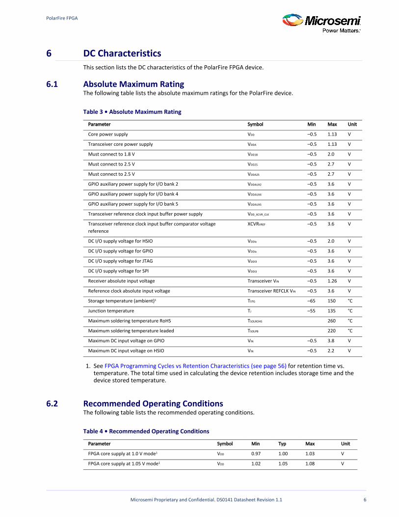
6 DC CharacteristicsThis section lists the DC characteristics of the PolarFire FPGA device.
6.1 Absolute Maximum RatingThe following table lists the absolute maximum ratings for the PolarFire device.
Table 3 • Absolute Maximum Rating
Parameter Symbol Min Max Unit
Core power supply VDD –0.5 1.13 V
Transceiver core power supply VDDA –0.5 1.13 V
Must connect to 1.8 V VDD18 –0.5 2.0 V
Must connect to 2.5 V VDD25 –0.5 2.7 V
Must connect to 2.5 V VDDA25 –0.5 2.7 V
GPIO auxiliary power supply for I/O bank 2 VDDAUX2 –0.5 3.6 V
GPIO auxiliary power supply for I/O bank 4 VDDAUX4 –0.5 3.6 V
GPIO auxiliary power supply for I/O bank 5 VDDAUX5 –0.5 3.6 V
Transceiver reference clock input buffer power supply VDD_XCVR_CLK –0.5 3.6 V
Transceiver reference clock input buffer comparator voltage reference
XCVRVREF –0.5 3.6 V
DC I/O supply voltage for HSIO VDDIx –0.5 2.0 V
DC I/O supply voltage for GPIO VDDIx –0.5 3.6 V
DC I/O supply voltage for JTAG VDDI3 –0.5 3.6 V
DC I/O supply voltage for SPI VDDI3 –0.5 3.6 V
Receiver absolute input voltage Transceiver VIN –0.5 1.26 V
Reference clock absolute input voltage Transceiver REFCLK VIN –0.5 3.6 V
Storage temperature (ambient)1 TSTG –65 150 °C
Junction temperature TJ –55 135 °C
Maximum soldering temperature RoHS TSOLROHS 260 °C
Maximum soldering temperature leaded TSOLPB 220 °C
Maximum DC input voltage on GPIO VIN –0.5 3.8 V
Maximum DC input voltage on HSIO VIN –0.5 2.2 V
See for retention time vs. FPGA Programming Cycles vs Retention Characteristics (see page 56)temperature. The total time used in calculating the device retention includes storage time and the device stored temperature.
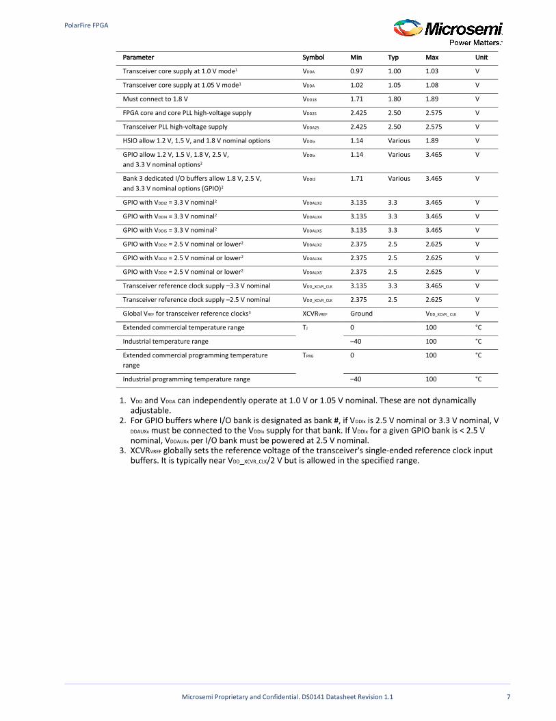
6.2 Recommended Operating ConditionsThe following table lists the recommended operating conditions.
Table 4 • Recommended Operating Conditions
Parameter Symbol Min Typ Max Unit
FPGA core supply at 1.0 V mode1 VDD 0.97 1.00 1.03 V
FPGA core supply at 1.05 V mode1 VDD 1.02 1.05 1.08 V
PolarFire FPGA
Microsemi Proprietary and Confidential. DS0141 Datasheet Revision 1.1 7
1.
2.
3.
Parameter Symbol Min Typ Max Unit
Transceiver core supply at 1.0 V mode1 VDDA 0.97 1.00 1.03 V
Transceiver core supply at 1.05 V mode1 VDDA 1.02 1.05 1.08 V
Must connect to 1.8 V VDD18 1.71 1.80 1.89 V
FPGA core and core PLL high-voltage supply VDD25 2.425 2.50 2.575 V
Transceiver PLL high-voltage supply VDDA25 2.425 2.50 2.575 V
HSIO allow 1.2 V, 1.5 V, and 1.8 V nominal options VDDIx 1.14 Various 1.89 V
GPIO allow 1.2 V, 1.5 V, 1.8 V, 2.5 V,and 3.3 V nominal options2
VDDIx 1.14 Various 3.465 V
Bank 3 dedicated I/O buffers allow 1.8 V, 2.5 V,and 3.3 V nominal options (GPIO)2
VDDI3 1.71 Various 3.465 V
GPIO with V = 3.3 V nominalDDI2 2 VDDAUX2 3.135 3.3 3.465 V
GPIO with V = 3.3 V nominalDDI4 2 VDDAUX4 3.135 3.3 3.465 V
GPIO with V = 3.3 V nominalDDI5 2 VDDAUX5 3.135 3.3 3.465 V
GPIO with V = 2.5 V nominal or lowerDDI2 2 VDDAUX2 2.375 2.5 2.625 V
GPIO with V = 2.5 V nominal or lowerDDI2 2 VDDAUX4 2.375 2.5 2.625 V
GPIO with V = 2.5 V nominal or lowerDDI2 2 VDDAUX5 2.375 2.5 2.625 V
Transceiver reference clock supply –3.3 V nominal VDD_XCVR_CLK 3.135 3.3 3.465 V
Transceiver reference clock supply –2.5 V nominal VDD_XCVR_CLK 2.375 2.5 2.625 V
Global V for transceiver reference clocksREF 3 XCVRVREF Ground VDD_XCVR_ CLK V
Extended commercial temperature range TJ 0 100 °C
Industrial temperature range –40 100 °C
Extended commercial programming temperaturerange
TPRG 0 100 °C
Industrial programming temperature range –40 100 °C
V and V can independently operate at 1.0 V or 1.05 V nominal. These are not dynamically DD DDA
adjustable.For GPIO buffers where I/O bank is designated as bank #, if V is 2.5 V nominal or 3.3 V nominal, VDDIx
must be connected to the V supply for that bank. If V for a given GPIO bank is < 2.5 V DDAUXx DDIx DDIx
nominal, V per I/O bank must be powered at 2.5 V nominal.DDAUXx
XCVR globally sets the reference voltage of the transceiver's single-ended reference clock input VREF
buffers. It is typically near V _ /2 V but is allowed in the specified range.DD XCVR_CLK
PolarFire FPGA
Microsemi Proprietary and Confidential. DS0141 Datasheet Revision 1.1 8
1. 2. 3.
4.
5. 6.
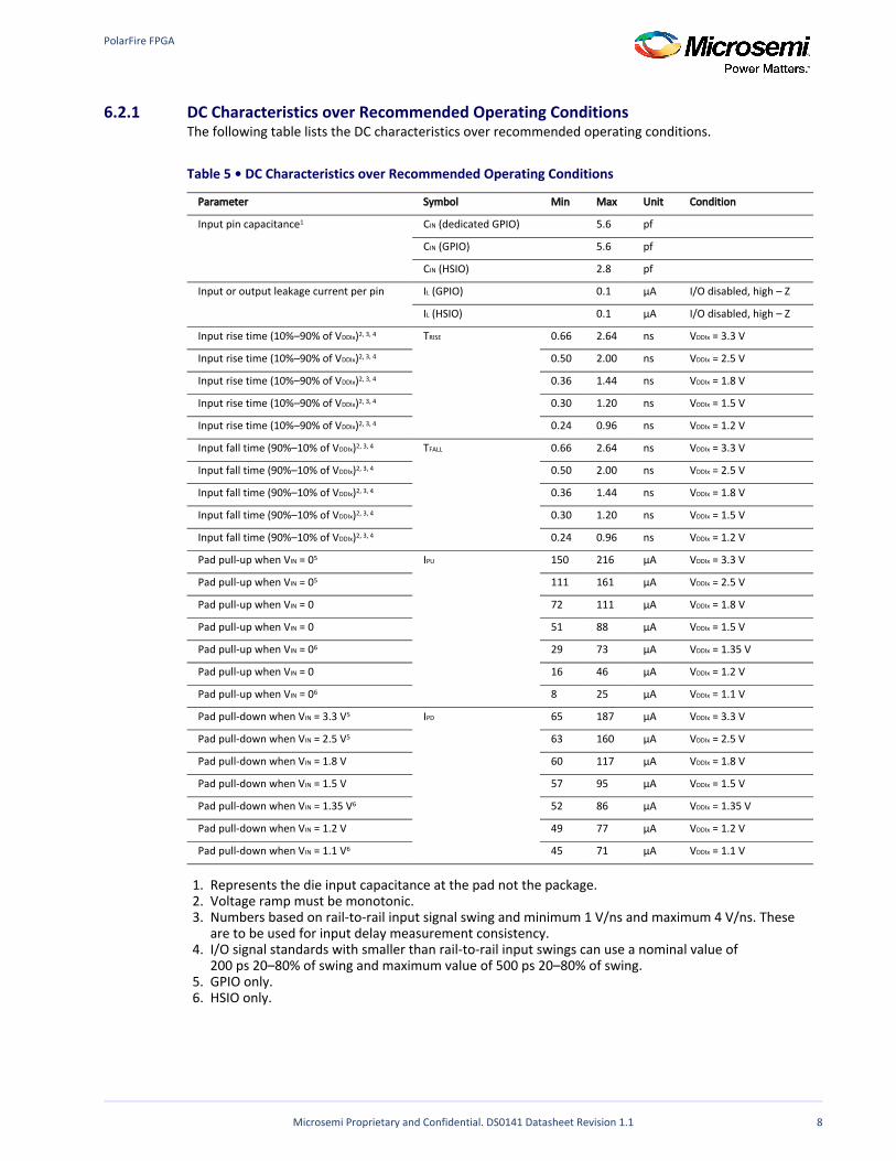
6.2.1 DC Characteristics over Recommended Operating ConditionsThe following table lists the DC characteristics over recommended operating conditions.
Table 5 • DC Characteristics over Recommended Operating Conditions
Parameter Symbol Min Max Unit Condition
Input pin capacitance1 C (dedicated GPIO)IN 5.6 pf
C (GPIO)IN 5.6 pf
C (HSIO)IN 2.8 pf
Input or output leakage current per pin I (GPIO)L 0.1 µA I/O disabled, high – Z
I (HSIO)L 0.1 µA I/O disabled, high – Z
Input rise time (10%–90% of V )DDIx 2, 3, 4 TRISE 0.66 2.64 ns V = 3.3 VDDIx
Input rise time (10%–90% of V )DDIx 2, 3, 4 0.50 2.00 ns V = 2.5 VDDIx
Input rise time (10%–90% of V )DDIx 2, 3, 4 0.36 1.44 ns V = 1.8 VDDIx
Input rise time (10%–90% of V )DDIx 2, 3, 4 0.30 1.20 ns V = 1.5 VDDIx
Input rise time (10%–90% of V )DDIx 2, 3, 4 0.24 0.96 ns V = 1.2 VDDIx
Input fall time (90%–10% of V )DDIx 2, 3, 4 TFALL 0.66 2.64 ns V = 3.3 VDDIx
Input fall time (90%–10% of V )DDIx 2, 3, 4 0.50 2.00 ns V = 2.5 VDDIx
Input fall time (90%–10% of V )DDIx 2, 3, 4 0.36 1.44 ns V = 1.8 VDDIx
Input fall time (90%–10% of V )DDIx 2, 3, 4 0.30 1.20 ns V = 1.5 VDDIx
Input fall time (90%–10% of V )DDIx 2, 3, 4 0.24 0.96 ns V = 1.2 VDDIx
Pad pull-up when V = 0IN 5 IPU 150 216 µA V = 3.3 VDDIx
Pad pull-up when V = 0IN 5 111 161 µA V = 2.5 VDDIx
Pad pull-up when V = 0IN 72 111 µA V = 1.8 VDDIx
Pad pull-up when V = 0IN 51 88 µA V = 1.5 VDDIx
Pad pull-up when V = 0IN 6 29 73 µA V = 1.35 VDDIx
Pad pull-up when V = 0IN 16 46 µA V = 1.2 VDDIx
Pad pull-up when V = 0IN 6 8 25 µA V = 1.1 VDDIx
Pad pull-down when V = 3.3 VIN 5 IPD 65 187 µA V = 3.3 VDDIx
Pad pull-down when V = 2.5 VIN 5 63 160 µA V = 2.5 VDDIx
Pad pull-down when V = 1.8 VIN 60 117 µA V = 1.8 VDDIx
Pad pull-down when V = 1.5 VIN 57 95 µA V = 1.5 VDDIx
Pad pull-down when V = 1.35 VIN 6 52 86 µA V = 1.35 VDDIx
Pad pull-down when V = 1.2 VIN 49 77 µA V = 1.2 VDDIx
Pad pull-down when V = 1.1 VIN 6 45 71 µA V = 1.1 VDDIx
Represents the die input capacitance at the pad not the package.Voltage ramp must be monotonic.Numbers based on rail-to-rail input signal swing and minimum 1 V/ns and maximum 4 V/ns. These are to be used for input delay measurement consistency.I/O signal standards with smaller than rail-to-rail input swings can use a nominal value of200 ps 20–80% of swing and maximum value of 500 ps 20–80% of swing.GPIO only.HSIO only.
PolarFire FPGA
Microsemi Proprietary and Confidential. DS0141 Datasheet Revision 1.1 9
1.
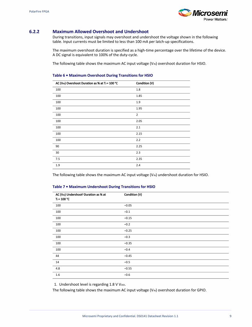
6.2.2 Maximum Allowed Overshoot and UndershootDuring transitions, input signals may overshoot and undershoot the voltage shown in the following table. Input currents must be limited to less than 100 mA per latch-up specifications.
The maximum overshoot duration is specified as a high-time percentage over the lifetime of the device. A DC signal is equivalent to 100% of the duty-cycle.
The following table shows the maximum AC input voltage (V ) overshoot duration for HSIO.IN
Table 6 • Maximum Overshoot During Transitions for HSIO
AC (V ) Overshoot Duration as % at TIN J = 100 °C Condition (V)
100 1.8
100 1.85
100 1.9
100 1.95
100 2
100 2.05
100 2.1
100 2.15
100 2.2
90 2.25
30 2.3
7.5 2.35
1.9 2.4
The following table shows the maximum AC input voltage (V ) undershoot duration for HSIO.IN
Table 7 • Maximum Undershoot During Transitions for HSIO
UndershootAC (V ) IN 1 Duration as % at TJ = 100 °C
Condition (V)
100 –0.05
100 –0.1
100 –0.15
100 –0.2
100 –0.25
100 –0.3
100 –0.35
100 –0.4
44 –0.45
14 –0.5
4.8 –0.55
1.6 –0.6
Undershoot level is regarding 1.8 V V .DDI
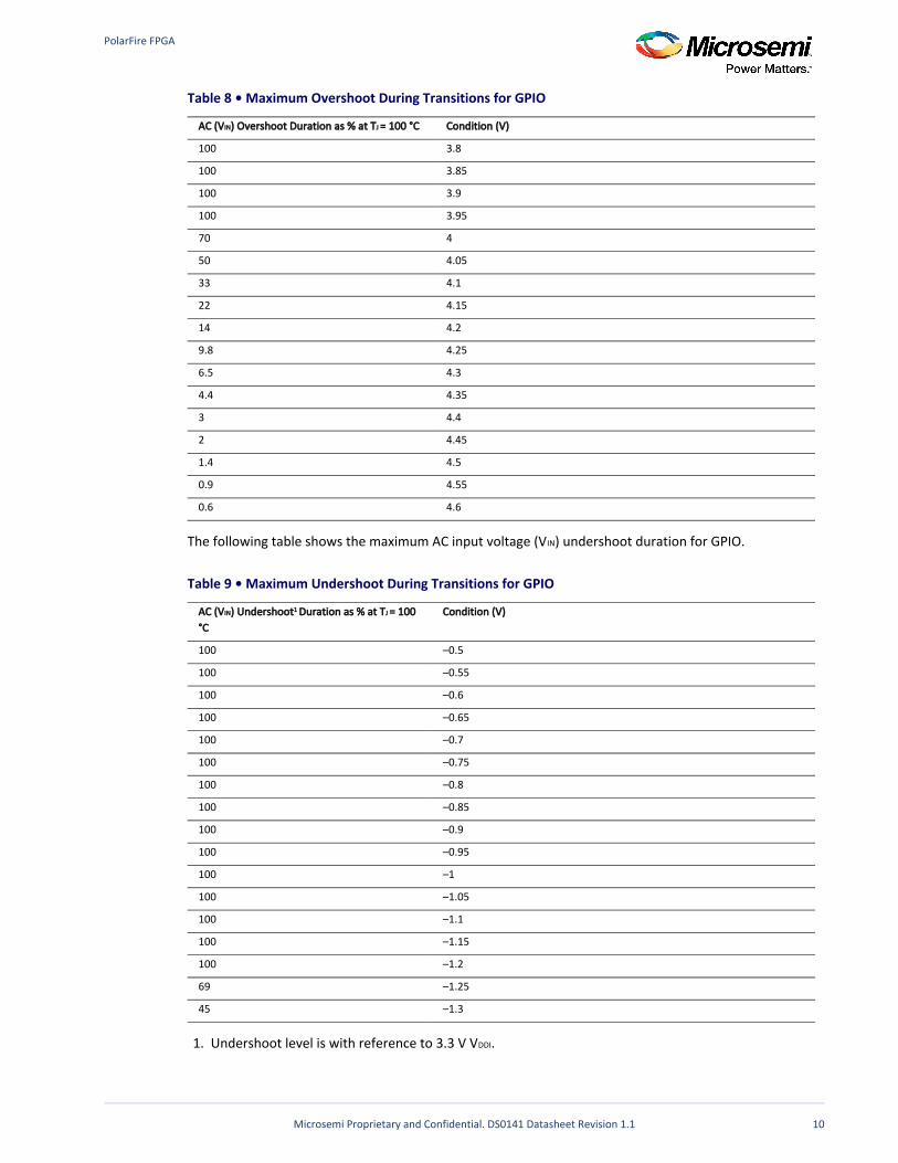
The following table shows the maximum AC input voltage (V ) overshoot duration for GPIO.IN
PolarFire FPGA
Microsemi Proprietary and Confidential. DS0141 Datasheet Revision 1.1 10
1.
Table 8 • Maximum Overshoot During Transitions for GPIO
Overshoot Duration as % at TAC (V ) IN J = 100 C° Condition (V)
100 3.8
100 3.85
100 3.9
100 3.95
70 4
50 4.05
33 4.1
22 4.15
14 4.2
9.8 4.25
6.5 4.3
4.4 4.35
3 4.4
2 4.45
1.4 4.5
0.9 4.55
0.6 4.6
The following table shows the maximum AC input voltage (V ) undershoot duration for GPIO.IN
Table 9 • Maximum Undershoot During Transitions for GPIO
UndershootAC (V ) IN 1 Duration as % at TJ = 100 °C
Condition (V)
100 –0.5
100 –0.55
100 –0.6
100 –0.65
100 –0.7
100 –0.75
100 –0.8
100 –0.85
100 –0.9
100 –0.95
100 –1
100 –1.05
100 –1.1
100 –1.15
100 –1.2
69 –1.25
45 –1.3
Undershoot level is with reference to 3.3 V V .DDI
PolarFire FPGA
Microsemi Proprietary and Confidential. DS0141 Datasheet Revision 1.1 11
1.
2. 3.
4.
5.
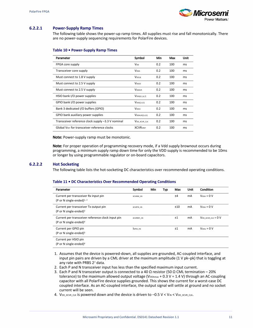
6.2.2.1 Power-Supply Ramp TimesThe following table shows the power-up ramp times. All supplies must rise and fall monotonically. There are no power-supply sequencing requirements for PolarFire devices.
Table 10 • Power-Supply Ramp Times
Parameter Symbol Min Max Unit
FPGA core supply VDD 0.2 100 ms
Transceiver core supply VDDA 0.2 100 ms
Must connect to 1.8 V supply VDD18 0.2 100 ms
Must connect to 2.5 V supply VDD25 0.2 100 ms
Must connect to 2.5 V supply VDDA25 0.2 100 ms
HSIO bank I/O power supplies VDDI[0,1,6,7] 0.2 100 ms
GPIO bank I/O power supplies VDDI[2,4,5] 0.2 100 ms
Bank 3 dedicated I/O buffers (GPIO) VDDI3 0.2 100 ms
GPIO bank auxiliary power supplies VDDAUX[2,4,5] 0.2 100 ms
Transceiver reference clock supply –3.3 V nominal VDD_XCVR_CLK 0.2 100 ms
Global V for transceiver reference clocksREF XCVRVREF 0.2 100 ms
Note: Power-supply ramp must be monotonic.
Note: For proper operation of programming recovery mode, if a Vdd supply brownout occurs during programming, a minimum supply ramp down time for only the VDD supply is recommended to be 10ms or longer by using programmable regulator or on-board capacitors.
6.2.2.2 Hot SocketingThe following table lists the hot-socketing DC characteristics over recommended operating conditions.
Table 11 • DC Characteristics Over Recommended Operating Conditions
Parameter Symbol Min Typ Max Unit Condition
Current per transceiver Rx input pin(P or N single-ended) 1, 2
XCVRRX_HS ±4 mA V = 0 VDDA
Current per transceiver Tx output pin(P or N single-ended)3
XCVRTX_HS ±10 mA V = 0 VDDA
Current per transceiver reference clock input pin(P or N single-ended)4
XCVRREF_HS ±1 mA V = 0 VDD_XCVR_CLK
Current per GPIO pin(P or N single-ended)5
IGPIO_HS ±1 mA V = 0 VDDIx
Current per HSIO pin(P or N single-ended)6
Assumes that the device is powered-down, all supplies are grounded, AC-coupled interface, and input pin pairs are driven by a CML driver at the maximum amplitude (1 V pk–pk) that is toggling at any rate with PRBS 2 data.7
Each P and N transceiver input has less than the specified maximum input current.Each P and N transceiver output is connected to a 40 Ω resistor (50 Ω CML termination – 20% tolerance) to the maximum allowed output voltage (V + 0.3 V = 1.4 V) through an AC-coupling DDAmax
capacitor with all PolarFire device supplies grounded. This shows the current for a worst-case DC coupled interface. As an AC-coupled interface, the output signal will settle at ground and no socket current will be seen.V is powered down and the device is driven to –0.5 V < V < V .DD_XCVR_CLK IN DD_XCVR_CLK
V is powered down and the device is driven to –0.5 V < V < GPIO V .DDIx IN DDImax
PolarFire FPGA
Microsemi Proprietary and Confidential. DS0141 Datasheet Revision 1.1 12
5. 6.
V is powered down and the device is driven to –0.5 V < V < GPIO V .DDIx IN DDImax
Not supported.
6.3 Input and OutputThe following section describes:
DC I/O levelsDifferential and complementary differential DC I/O levelsHSIO and GPIO on-die termination specificationsLVDS specifications
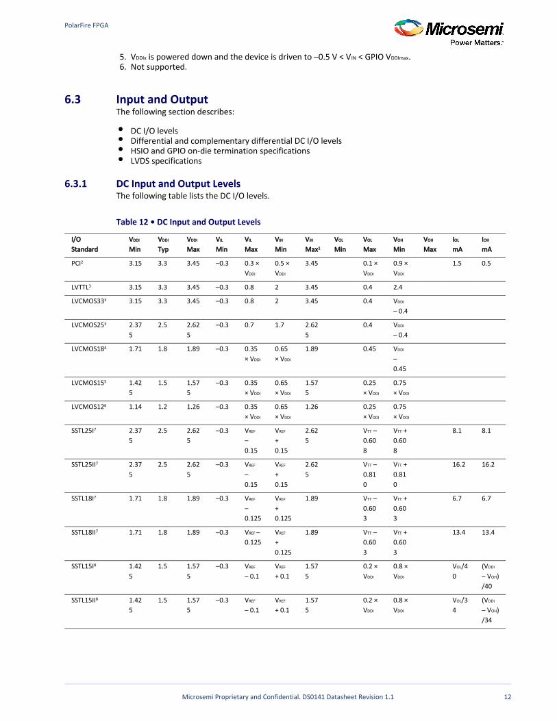
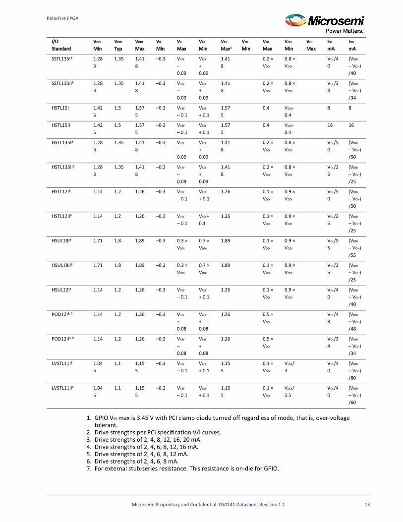
6.3.1 DC Input and Output LevelsThe following table lists the DC I/O levels.
Table 12 • DC Input and Output Levels
I/OStandard
VDDI
MinVDDI
TypVDDI
MaxVIL
MinVIL
MaxVIH
MinVIH
Max1
VOL
MinVOL
MaxVOH
MinVOH
MaxIOL
mAIOH
mA
PCI2 3.15 3.3 3.45 –0.3 0.3 × VDDI
0.5 × VDDI
3.45 0.1 × VDDI
0.9 × VDDI
1.5 0.5
LVTTL3 3.15 3.3 3.45 –0.3 0.8 2 3.45 0.4 2.4
LVCMOS333 3.15 3.3 3.45 –0.3 0.8 2 3.45 0.4 V DDI
– 0.4
LVCMOS253 2.375
2.5 2.625
–0.3 0.7 1.7 2.625
0.4 V DDI
– 0.4
LVCMOS184 1.71 1.8 1.89 –0.3 0.35 × VDDI
0.65 × VDDI
1.89 0.45 V DDI
– 0.45
LVCMOS155 1.425
1.5 1.575
–0.3 0.35 × VDDI
0.65 × VDDI
1.575
0.25 × VDDI
0.75 × VDDI
LVCMOS126 1.14 1.2 1.26 –0.3 0.35 × VDDI
0.65 × VDDI
1.26 0.25 × VDDI
0.75 × VDDI
SSTL25I7 2.375
2.5 2.625
–0.3 V REF
– 0.15
V REF
+ 0.15
2.625
V – TT
0.608
V + TT
0.608
8.1 8.1
SSTL25II7 2.375
2.5 2.625
–0.3 V REF
– 0.15
V REF
+ 0.15
2.625
V – TT
0.810
V + TT
0.810
16.2 16.2
SSTL18I7 1.71 1.8 1.89 –0.3 V REF
– 0.125
V REF
+ 0.125
1.89 V – TT
0.603
V + TT
0.603
6.7 6.7
SSTL18II7 1.71 1.8 1.89 –0.3 V –REF
0.125V REF
+ 0.125
1.89 V – TT
0.603
V + TT
0.603
13.4 13.4
SSTL15I8 1.425
1.5 1.575
–0.3 V REF
– 0.1V REF
+ 0.11.575
0.2 × VDDI
0.8 × VDDI
V /4OL
0(V DDI
– V )OH
/40
SSTL15II8 1.425
1.5 1.575
–0.3 V REF
– 0.1V REF
+ 0.11.575
0.2 × VDDI
0.8 × VDDI
V /3OL
4(V DDI
– V )OH
/34
PolarFire FPGA
Microsemi Proprietary and Confidential. DS0141 Datasheet Revision 1.1 13
1.
2. 3. 4. 5. 6. 7.
8.
I/OStandard
VDDI
MinVDDI
TypVDDI
MaxVIL
MinVIL
MaxVIH
MinVIH
Max1
VOL
MinVOL
MaxVOH
MinVOH
MaxIOL
mAIOH
mA
SSTL135I8 1.283
1.35 1.418
–0.3 V REF
– 0.09
V REF
+ 0.09
1.418
0.2 × VDDI
0.8 × VDDI
V /4OL
0(V DDI
– V )OH
/40
SSTL135II8 1.283
1.35 1.418
–0.3 V REF
– 0.09
V REF
+ 0.09
1.418
0.2 × VDDI
0.8 × VDDI
V /3OL
4(V DDI
– V )OH
/34
HSTL15I 1.425
1.5 1.575
–0.3 V REF
– 0.1V REF
+ 0.11.575
0.4 V -DDI
0.4 8 8
HSTL15II 1.425
1.5 1.575
–0.3 V REF
– 0.1V REF
+ 0.11.575
0.4 V -DDI
0.4 16 16
HSTL135I8 1.283
1.35 1.418
–0.3 V REF
– 0.09
V REF
+ 0.09
1.418
0.2 × VDDI
0.8 × VDDI
V /5OL
0(V DDI
– V )OH
/50
HSTL135II8 1.283
1.35 1.418
–0.3 V REF
– 0.09
V REF
+ 0.09
1.418
0.2 × VDDI
0.8 × VDDI
V /2OL
5(V DDI
– V )OH
/25
HSTL12I8 1.14 1.2 1.26 –0.3 V REF
– 0.1V REF
+ 0.11.26 0.1 ×
VDDI
0.9 × VDDI
V /5OL
0(V DDI
– V )OH
/50
HSTL12II8 1.14 1.2 1.26 –0.3 V REF
– 0.1V +REF
0.11.26 0.1 ×
VDDI
0.9 × VDDI
V /2OL
5(V DDI
– V )OH
/25
HSUL18I8 1.71 1.8 1.89 –0.3 0.3 × VDDI
0.7 × VDDI
1.89 0.1 × VDDI
0.9 × VDDI
V /5OL
5(V DDI
– V )OH
/55
HSUL18II8 1.71 1.8 1.89 –0.3 0.3 × VDDI
0.7 × VDDI
1.89 0.1 × VDDI
0.9 × VDDI
V /2OL
5(V DDI
– V )OH
/25
HSUL12I8 1.14 1.2 1.26 –0.3 V REF
– 0.1V REF
+ 0.11.26 0.1 ×
VDDI
0.9 × VDDI
V /4OL
0(V DDI
– V )OH
/40
POD12I8, 9 1.14 1.2 1.26 –0.3 V REF
– 0.08
V REF
+ 0.08
1.26 0.5 × VDDI
V /4OL
8(V DDI
– V )OH
/48
POD12II8, 9 1.14 1.2 1.26 –0.3 V REF
– 0.08
V REF
+ 0.08
1.26 0.5 × VDDI
V /3OL
4(V DDI
– V )OH
/34
LVSTL11I8 1.045
1.1 1.155
–0.3 V REF
– 0.1V REF
+ 0.11.155
0.1 × VDDI
V /DDI
3 V /4OL
0(V DDI
– V )OH
/80
LVSTL11II8 1.045
1.1 1.155
–0.3 V REF
– 0.1V REF
+ 0.11.155
0.1 × VDDI
V /DDI
2.5 V /4OL
0(V DDI
– V )OH
/60
GPIO V max is 3.45 V with PCI clamp diode turned off regardless of mode, that is, over-voltage IH
tolerant.Drive strengths per PCI specification V/I curves.Drive strengths of 2, 4, 8, 12, 16, 20 mA.Drive strengths of 2, 4, 6, 8, 12, 16 mA.Drive strengths of 2, 4, 6, 8, 12 mA.Drive strengths of 2, 4, 6, 8 mA.For external stub-series resistance. This resistance is on-die for GPIO.
I /I Units for impedance standards in Amps (not mA).OL OH
PolarFire FPGA
Microsemi Proprietary and Confidential. DS0141 Datasheet Revision 1.1 14
8. 9.
I /I Units for impedance standards in Amps (not mA).OL OH
VOH_MAX based on external pull-up termination (pseudo-open drain).Note: 3.3 V and 2.5 V are only supported in GPIO banks.
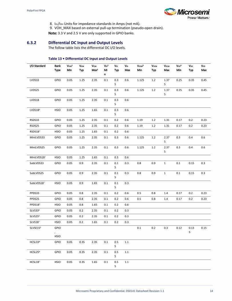
6.3.2 Differential DC Input and Output LevelsThe follow table lists the differential DC I/O levels.
Table 13 • Differential DC Input and Output Levels
I/O Standard BankType
VICM1
MinVICM
TypVICM
Max5
VID2
Min
VID
TypVID
MaxVOCM3
MinVOCM
TypVOCM
MaxVOD4
MinVOD
TypVOD
Max
LVDS33 GPIO 0.05 1.25 2.35 0.1 0.35
0.6 1.125 1.2 1.375
0.25 0.35 0.45
LVDS25 GPIO 0.05 1.25 2.35 0.1 0.35
0.6 1.125 1.2 1.375
0.25 0.35 0.45
LVDS18 GPIO 0.05 1.25 2.35 0.1 0.35
0.6
LVDS186 HSIO 0.05 1.25 1.65 0.1 0.35
0.6
RSDS33 GPIO 0.05 1.25 2.35 0.1 0.2 0.6 1.19 1.2 1.31 0.17 0.2 0.23
RSDS25 GPIO 0.05 1.25 2.35 0.1 0.2 0.6 1.19 1.2 1.31 0.17 0.2 0.23
RSDS187 HSIO 0.05 1.25 1.65 0.1 0.2 0.6
MiniLVDS33 GPIO 0.05 1.25 2.35 0.1 0.3 0.6 1.125 1.2 2.375
0.3 0.4 0.6
MiniLVDS25 GPIO 0.05 1.25 2.35 0.1 0.3 0.6 1.125 1.2 2.375
0.3 0.4 0.6
MiniLVDS187 HSIO 0.05 1.25 1.65 0.1 0.3 0.6
SubLVDS33 GPIO 0.05 0.9 2.35 0.1 0.15
0.3 0.8 0.9 1 0.1 0.15 0.3
SubLVDS25 GPIO 0.05 0.9 2.35 0.1 0.15
0.3 0.8 0.9 1 0.1 0.15 0.3
SubLVDS187 HSIO 0.05 0.9 1.65 0.1 0.15
0.3
PPDS33 GPIO 0.05 0.8 2.35 0.1 0.2 0.6 0.5 0.8 1.4 0.17 0.2 0.23
PPDS25 GPIO 0.05 0.8 2.35 0.1 0.2 0.6 0.5 0.8 1.4 0.17 0.2 0.23
PPDS187 HSIO 0.05 0.8 1.65 0.1 0.2 0.6
SLVS338 GPIO 0.05 0.2 2.35 0.1 0.2 0.3
SLVS258 GPIO 0.05 0.2 2.35 0.1 0.2 0.3
SLVS187 HSIO 0.05 0.2 1.65 0.1 0.2 0.3
SLVSE159 GPIO, HSIO
0.1 0.2 0.3 0.12 0.135
0.15
HCSL338 GPIO 0.05 0.35 2.35 0.1 0.55
1.1
HCSL258 GPIO 0.05 0.35 2.35 0.1 0.55
1.1
HCSL187 HSIO 0.05 0.35 1.65 0.1 0.55
1.1
PolarFire FPGA
Microsemi Proprietary and Confidential. DS0141 Datasheet Revision 1.1 15
1. 2. 3. 4. 5. 6. 7. 8. 9.
I/O Standard BankType
VICM1
MinVICM
TypVICM
Max5
VID2
Min
VID
TypVID
MaxVOCM3
MinVOCM
TypVOCM
MaxVOD4
MinVOD
TypVOD
Max
BUSLVDSE259 GPIO 0.05 1.25 2.35 0.05
0.1 VDDIn 1.15 1.25 1.31 0.24 0.262
0.272
MLVDSE259 GPIO 0.05 1.25 2.35 0.05
0.35
2.4 1.15 1.25 1.31 0.396
0.442
0.453
LVPECL339 GPIO 0.05 1.65 2.35 0.05
0.8 2.4 1.51 1.65 1.74 0.664
0.722
0.755
LVPECLE339 GPIO 0.05 1.65 2.35 0.05
0.8 2.4 1.51 1.65 1.74 0.664
0.722
0.755
MIPIE259 GPIO 0.05 0.2 2.35 0.05
0.2 0.3 0.15 0.25 0.35 0.1 0.22 0.3
MIPI12 (high-speed)
GPIO 0.05 0.2 2.35 0.05
0.2 0.3
V is the input common mode.ICM
V is the input differential voltage.ID
V is the output common mode voltage.OCM
V is the output differential voltage.OD
V must be less than V – .3 V.ICM DDI
HSIO receiver only, for AC transient purposes, V cannot exceed 0.95 V.ICM
HSIO receiver only.GPIO receiver only.Emulated output only.
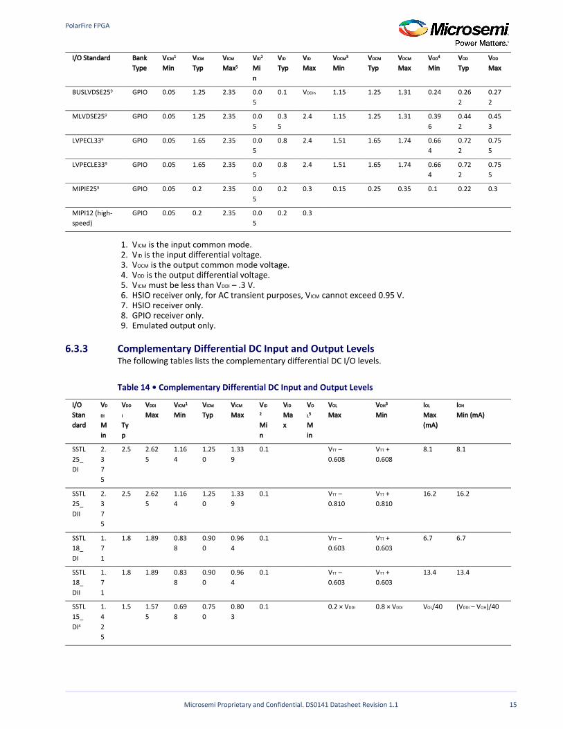
6.3.3 Complementary Differential DC Input and Output LevelsThe following tables lists the complementary differential DC I/O levels.
Table 14 • Complementary Differential DC Input and Output Levels
I/O Standard
VD
DI
Min
VDD
I
Typ
VDDI
MaxVICM1
MinVICM
TypVICM
MaxVID
2
Min
VID
Max
VO
L3
Min
VOL
MaxVOH3
MinIOL
Max (mA)
IOH
Min (mA)
SSTL25_DI
2.375
2.5 2.625
1.164
1.250
1.339
0.1 V – TT
0.608V + TT
0.6088.1 8.1
SSTL25_DII
2.375
2.5 2.625
1.164
1.250
1.339
0.1 V – TT
0.810V + TT
0.81016.2 16.2
SSTL18_DI
1.71
1.8 1.89 0.838
0.900
0.964
0.1 V – TT
0.603V + TT
0.6036.7 6.7
SSTL18_DII
1.71
1.8 1.89 0.838
0.900
0.964
0.1 V – TT
0.603V + TT
0.60313.4 13.4
SSTL15_DI4
1.425
1.5 1.575
0.698
0.750
0.803
0.1 0.2 × VDDI 0.8 × VDDI V /40OL (V – V )/40DDI OH
PolarFire FPGA
Microsemi Proprietary and Confidential. DS0141 Datasheet Revision 1.1 16
I/O Standard
VD
DI
Min
VDD
I
Typ
VDDI
MaxVICM1
MinVICM
TypVICM
MaxVID
2
Min
VID
Max
VO
L3
Min
VOL
MaxVOH3
MinIOL
Max (mA)
IOH
Min (mA)
SSTL15_DII4
1.425
1.5 1.575
0.698
0.750
0.803
0.1 0.2 × VDDI 0.8 × VDDI V /34OL (V – V )/34DDI OH
SSTL135_DI4
1.283
1.35
1.418
0.629
0.675
0.723
0.1 0.2 × VDDI 0.8 × VDDI V /40OL (V – V )/40DDI OH
SSTL135_DII4
1.283
1.35
1.418
0.629
0.675
0.723
0.1 0.2 × VDDI 0.8 × VDDI V /34OL (V – V )/34DDI OH
HSTL15_DI
1.425
1.5 1.575
0.698
0.750
0.803
0.1 0.4 V – 0.4DDI 8 8
HSTL15_DII
1.425
1.5 1.575
0.698
0.750
0.803
0.1 0.4 V – 0.4DDI 16 16
HSTL135_DI4
1.283
1.35
1.418
0.629
0.675
0.723
0.1 0.2 × VDDI 0.8 × VDDI V /50OL (V – V )/50DDI OH
HSTL135_DII4
1.283
1.35
1.418
0.629
0.675
0.723
0.1 0.2 × VDDI 0.8 × VDDI V /25OL (V – V )/25DDI OH
HSTL12_DI4
1.14
1.2 1.26 0.559
0.600
0.643
0.1 0.1 × VDDI 0.9 × VDDI V /50OL (V – V )/50DDI OH
HSUL18_DI4
1.71
1.8 1.89 0.838
0.900
0.964
0.1 0.1 × VDDI 0.9 × VDDI V /55OL (V – V )/55DDI OH
HSUL18_DII4
1.71
1.8 1.89 0.838
0.900
0.964
0.1 0.1 × VDDI 0.9 × VDDI V /25OL (V – V )/25DDI OH
HSUL12_DI4
1.14
1.2 1.26 0.559
0.600
0.643
0.1 0.1 × VDDI 0.9 × VDDI V /40OL (V – V )/40DDI OH
POD12_DI4, 5
1.14
1.2 1.26 0.787
0.840
0.895
0.1 0.5 × VDDI V /48OL (V – V )/48DDI OH
POD12_DII4,
5
1.14
1.2 1.26 0.787
0.840
0.895
0.1 0.5 × VDDI V /34OL (V – V )/34DDI OH
PolarFire FPGA
Microsemi Proprietary and Confidential. DS0141 Datasheet Revision 1.1 17
1. 2. 3. 4. 5.
I/O Standard
VD
DI
Min
VDD
I
Typ
VDDI
MaxVICM1
MinVICM
TypVICM
MaxVID
2
Min
VID
Max
VO
L3
Min
VOL
MaxVOH3
MinIOL
Max (mA)
IOH
Min (mA)
LVSTL11_DI4
1.045
1.1 1.155
0.172
0.183
0.194
0.1 0.1 × VDDI V /3DDI V /40OL (V – V )/80DDI OH
LVSTL11_DII4
1.045
1.1 1.155
0.207
0.220
0.233
0.1 0.1 × VDDI V /2.5DDI V /40OL (V – V )/60DDI OH
V is the input common mode voltage.ICM
V is the input differential voltage (Q – Q).ID
V is the single-ended high-output voltage.OH
I /I Units for impedance standards in Amps (not mA).OL OH
V based on external pull-up termination (pseudo-open drain).OH_MAX
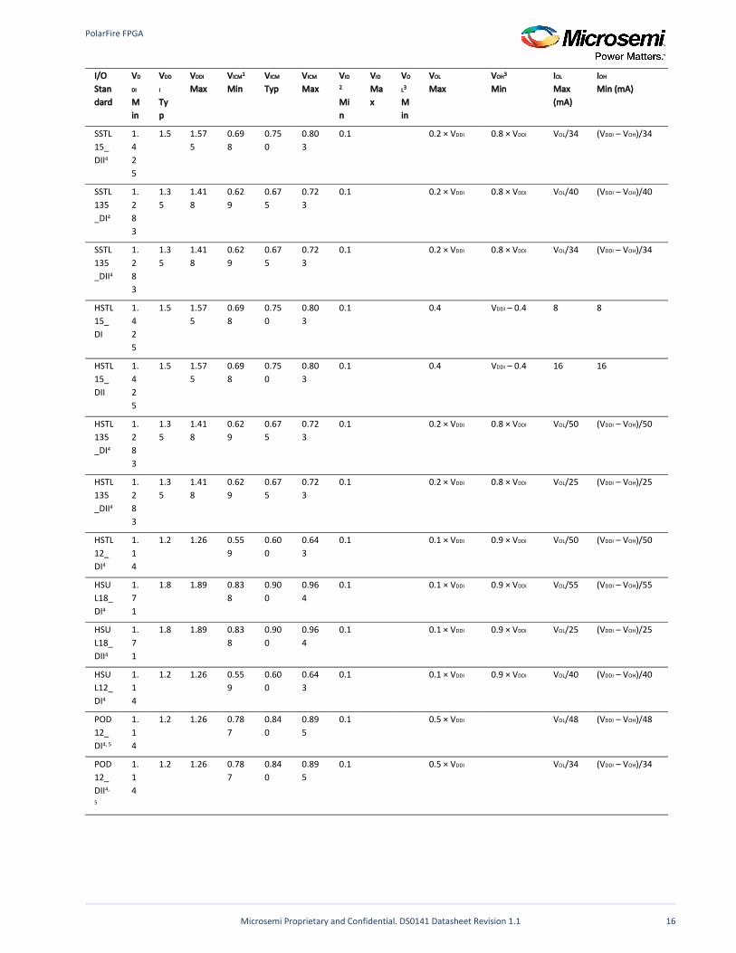
6.3.4 HSIO On-Die TerminationThe following tables lists the on-die termination calibration accuracy specifications for HSIO bank.
Table 15 • Single-Ended Thevenin Termination (Internal Parallel Thevenin Termination)
Min (%) Typ Max (%) Unit Condition
–40 50 20 Ω V = 1.8 V/1.5 V/1.35 V/1.2 VDDI
–40 75 20 Ω V = 1.8 VDDI
–40 150 20 Ω V = 1.8 VDDI
–20 20 20 Ω V = 1.5 V/1.35 VDDI
–20 30 20 Ω V = 1.5 V/1.35 VDDI
–20 40 20 Ω V = 1.5 V/1.35 VDDI
–20 60 20 Ω V = 1.5 V/1.35 VDDI
–20 120 20 Ω V = 1.5 V/1.35 VDDI
–20 60 20 Ω V = 1.2 VDDI
–20 120 20 Ω V = 1.2 VDDI
Note: The venin impedance is calculated based on independent P and N as measured at 50% of V . For DDI
50 Ω/75 Ω/150 Ω cases, nearest supported values of 40 Ω/60 Ω/120 Ω are used.
Table 16 • Single-Ended Termination to VDDI (Internal Parallel Termination to VDDI)
Min (%) Typ Max (%) Unit Condition
–20 120 20 Ω V = 1.8 V/1.5 VDDI
–20 240 20 Ω V = 1.8 V/1.5 VDDI
–20 34 20 Ω V = 1.2 VDDI
–20 40 20 Ω V = 1.2 VDDI
–20 48 20 Ω V = 1.2 VDDI
–20 60 20 Ω V = 1.2 VDDI
–20 80 20 Ω V = 1.2 VDDI
–20 120 20 Ω V = 1.2 VDDI
PolarFire FPGA
Microsemi Proprietary and Confidential. DS0141 Datasheet Revision 1.1 18
Min (%) Typ Max (%) Unit Condition
–20 240 20 Ω V = 1.2 VDDI
Note: Measured at 50% of V .DDI
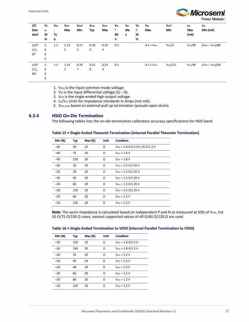
Table 17 • Single-Ended Termination to VSS (Internal Parallel Termination to VSS)
Min (%) Typ Max (%) Unit Condition
–20 120 20 Ω V = 1.8 V/1.5 VDDI
–20 240 20 Ω V = 1.8 V/1.5 VDDI
–20 120 20 Ω V = 1.2 VDDI
–20 240 20 Ω V = 1.2 VDDI
–20 40 20 Ω V = 1.1 VDDI
–20 48 20 Ω V = 1.1 VDDI
–20 60 20 Ω V = 1.1 VDDI
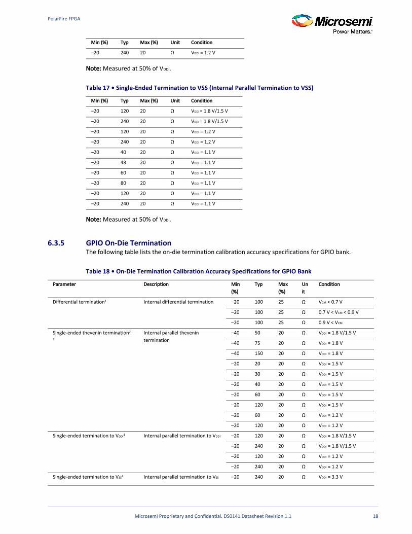
–20 80 20 Ω V = 1.1 VDDI
–20 120 20 Ω V = 1.1 VDDI
–20 240 20 Ω V = 1.1 VDDI
Note: Measured at 50% of V .DDI
6.3.5 GPIO On-Die TerminationThe following table lists the on-die termination calibration accuracy specifications for GPIO bank.
Table 18 • On-Die Termination Calibration Accuracy Specifications for GPIO Bank
Parameter Description Min (%)
Typ Max (%)
Unit
Condition
Differential termination1 Internal differential termination –20 100 25 Ω V < 0.7 VCM
–20 100 25 Ω 0.7 V < V < 0.9 VCM
–20 100 25 Ω 0.9 V < VCM
Single-ended thevenin termination2,
3
Internal parallel thevenin termination
–40 50 20 Ω V = 1.8 V/1.5 VDDI
–40 75 20 Ω V = 1.8 VDDI
–40 150 20 Ω V = 1.8 VDDI
–20 20 20 Ω V = 1.5 VDDI
–20 30 20 Ω V = 1.5 VDDI
–20 40 20 Ω V = 1.5 VDDI
–20 60 20 Ω V = 1.5 VDDI
–20 120 20 Ω V = 1.5 VDDI
–20 60 20 Ω V = 1.2 VDDI
–20 120 20 Ω V = 1.2 VDDI
Single-ended termination to VDDI4 Internal parallel termination to VDDI –20 120 20 Ω V = 1.8 V/1.5 VDDI
–20 240 20 Ω V = 1.8 V/1.5 VDDI
–20 120 20 Ω V = 1.2 VDDI
–20 240 20 Ω V = 1.2 VDDI
Single-ended termination to VSS4 Internal parallel termination to VSS –20 240 20 Ω V = 3.3 VDDI
PolarFire FPGA
Microsemi Proprietary and Confidential. DS0141 Datasheet Revision 1.1 19
1. 2. 3. 4.
1.
1.
2.
1.
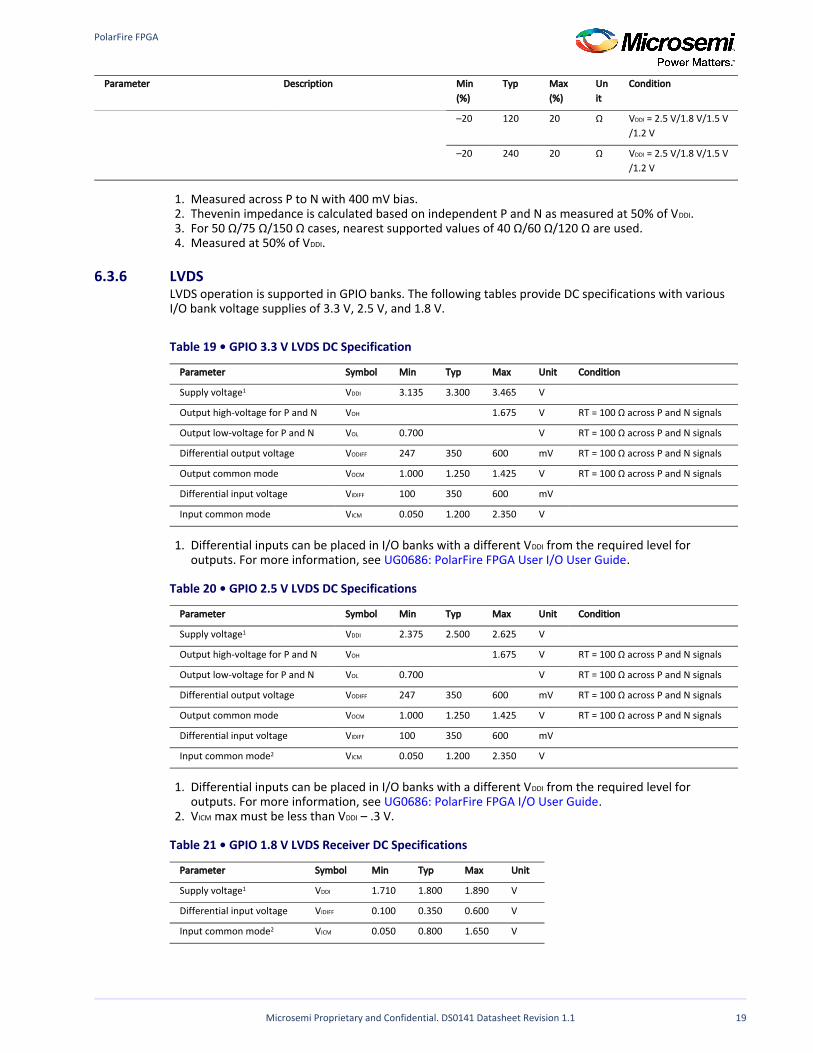
Parameter Description Min (%)
Typ Max (%)
Unit
Condition
–20 120 20 Ω V = 2.5 V/1.8 V/1.5 VDDI
/1.2 V
–20 240 20 Ω V = 2.5 V/1.8 V/1.5 VDDI
/1.2 V
Measured across P to N with 400 mV bias.Thevenin impedance is calculated based on independent P and N as measured at 50% of V .DDI
For 50 Ω/75 Ω/150 Ω cases, nearest supported values of 40 Ω/60 Ω/120 Ω are used.Measured at 50% of V .DDI
6.3.6 LVDSLVDS operation is supported in GPIO banks. The following tables provide DC specifications with variousI/O bank voltage supplies of 3.3 V, 2.5 V, and 1.8 V.
Table 19 • GPIO 3.3 V LVDS DC Specification
Parameter Symbol Min Typ Max Unit Condition
Supply voltage1 VDDI 3.135 3.300 3.465 V
Output high-voltage for P and N VOH 1.675 V RT = 100 Ω across P and N signals
Output low-voltage for P and N VOL 0.700 V RT = 100 Ω across P and N signals
Differential output voltage VODIFF 247 350 600 mV RT = 100 Ω across P and N signals
Output common mode VOCM 1.000 1.250 1.425 V RT = 100 Ω across P and N signals
Differential input voltage VIDIFF 100 350 600 mV
Input common mode VICM 0.050 1.200 2.350 V
Differential inputs can be placed in I/O banks with a different V from the required level for DDI
outputs. For more information, see .UG0686: PolarFire FPGA User I/O User Guide
Table 20 • GPIO 2.5 V LVDS DC Specifications
Parameter Symbol Min Typ Max Unit Condition
Supply voltage1 VDDI 2.375 2.500 2.625 V
Output high-voltage for P and N VOH 1.675 V RT = 100 Ω across P and N signals
Output low-voltage for P and N VOL 0.700 V RT = 100 Ω across P and N signals
Differential output voltage VODIFF 247 350 600 mV RT = 100 Ω across P and N signals
Output common mode VOCM 1.000 1.250 1.425 V RT = 100 Ω across P and N signals
Differential input voltage VIDIFF 100 350 600 mV
Input common mode2 VICM 0.050 1.200 2.350 V
Differential inputs can be placed in I/O banks with a different V from the required level for DDI
outputs. For more information, see .UG0686: PolarFire FPGA I/O User GuideV max must be less than V – .3 V.ICM DDI
Table 21 • GPIO 1.8 V LVDS Receiver DC Specifications
Parameter Symbol Min Typ Max Unit
Supply voltage1 VDDI 1.710 1.800 1.890 V
Differential input voltage VIDIFF 0.100 0.350 0.600 V
Input common mode2 VICM 0.050 0.800 1.650 V
Differential inputs can be placed in I/O banks with a different V from the required level for DDI
PolarFire FPGA
Microsemi Proprietary and Confidential. DS0141 Datasheet Revision 1.1 20
1.
2.
Differential inputs can be placed in I/O banks with a different V from the required level for DDI
outputs. For more information, see .UG0686: PolarFire FPGA I/O User GuideFor LVDS18, AC transient purposes, V cannot exceed 0.95 V.ICM
PolarFire FPGA
Microsemi Proprietary and Confidential. DS0141 Datasheet Revision 1.1 21
7 AC Switching CharacteristicsThis section contains the AC switching characteristics of the PolarFire devices.
7.1 I/O Standards SpecificationsThis section describes I/O delay measurement methodology, buffer speed, switching characteristics, digital latency, gearing training calibration, and maximum physical interface (PHY) rate for memory interface IP.
7.1.1 Input Delay Measurement MethodologyThe following table provides information about the methodology for input delay measurement.
Table 22 • Input Delay Measurement Methodology
Standard Description VL1 VH1 VID2 VICM2 VMEAS3, 4 VREF1, 5 Unit
PCI33 PCIE 3.3 V 0.1 3.2 1.32 V
LVTTL33 LVTTL 3.3 V 0.1 3.2 1.75 V
LVCMOS33 LVCMOS 3.3 V 0.1 3.2 1.75 V
LVCMOS25 LVCMOS 2.5 V 0.1 2.4 1.25 V
LVCMOS18 LVCMOS 1.8 V 0.1 1.7 0.90 V
LVCMOS15 LVCMOS 1.5 V 0.1 1.4 0.75 V
LVCMOS12 LVCMOS 1.2 V 0.1 1.1 0.60 V
SSTL25_I SSTL 2.5 V Class I
V – 1.15REF V + 1.15REF VREF 1.25 V
SSTL25_II SSTL 2.5 V Class II
V – 1.15REF V + 1.15REF VREF 1.25 V
SSTL18_I SSTL 1.8 V Class I
V – 0.8REF V + 0.8REF VREF 0.90 V
SSTL18_II SSTL 1.8 V Class II
V – 0.8REF V + 0.8REF VREF 0.90 V
SSTL15_I SSTL 1.5 V Class I
V – .65REF V + .65REF VREF 0.75 V
SSTL15_II SSTL 1.5 V Class II
V – .65REF V + .65REF VREF 0.75 V
SSTL135_I SSTL 1.35 V Class I
V – 575REF V + .575REF VREF 0.675 V
SSTL135_II SSTL 1.35 V Class II
V – .575REF V + .575REF VREF 0.675 V
HSTL15_I HSTL 1.5 V Class I
V – .65REF V + .65REF VREF 0.75 V
HSTL15_II HSTL 1.5 V Class II
V – .65REF V + .65REF VREF 0.75 V
HSTL135_I HSTL 1.35 V Class I
V – 575REF V + .575REF VREF 0.675 V
HSTL135_II HSTL 1.35 V Class II
V – .575REF V + .575REF VREF 0.675 V
HSTL12 HSTL 1.2 V V – .5REF V + .5REF VREF 0.60 V
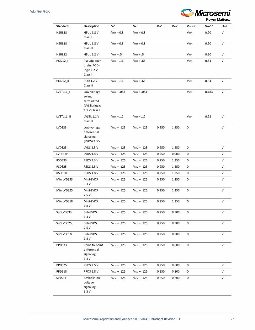
PolarFire FPGA
Microsemi Proprietary and Confidential. DS0141 Datasheet Revision 1.1 22
Standard Description VL1 VH1 VID2 VICM2 VMEAS3, 4 VREF1, 5 Unit
HSUL18_I HSUL 1.8 V Class I
V – 0.8REF V + 0.8REF VREF 0.90 V
HSUL18_II HSUL 1.8 V Class II
V – 0.8REF V + 0.8REF VREF 0.90 V
HSUL12 HSUL 1.2 V V – .5REF V + .5REF VREF 0.60 V
POD12_I Pseudo open drain (POD) logic 1.2 V Class I
V – .16REF V + .65REF VREF 0.84 V
POD12_II POD 1.2 V Class II
V – .16REF V + .65REF VREF 0.84 V
LVSTL11_I Low-voltage swing terminated (LVSTL) logic 1.1 V Class I
V – .083REF V + .083REF VREF 0.183 V
LVSTL11_II LVSTL 1.1 V Class II
V – .12REF V + .12REF VREF 0.22 V
LVDS33 Low-voltage differential signaling (LVDS) 3.3 V
V – .125ICM V + .125ICM 0.250 1.250 0 V
LVDS25 LVDS 2.5 V V – .125ICM V + .125ICM 0.250 1.250 0 V
LVDS186 LVDS 1.8 V V – .125ICM V + .125ICM 0.250 0.900 0 V
RSDS33 RSDS 3.3 V V – .125ICM V + .125ICM 0.250 1.250 0 V
RSDS25 RSDS 2.5 V V – .125ICM V + .125ICM 0.250 1.250 0 V
RSDS18 RSDS 1.8 V V – .125ICM V + .125ICM 0.250 1.250 0 V
MiniLVDS33 Mini-LVDS3.3 V
V – .125ICM V + .125ICM 0.250 1.250 0 V
MiniLVDS25 Mini-LVDS2.5 V
V – .125ICM V + .125ICM 0.250 1.250 0 V
MiniLVDS18 Mini-LVDS1.8 V
V – .125ICM V + .125ICM 0.250 1.250 0 V
SubLVDS33 Sub-LVDS3.3 V
V – .125ICM V + .125ICM 0.250 0.900 0 V
SubLVDS25 Sub-LVDS2.5 V
V – .125ICM V + .125ICM 0.250 0.900 0 V
SubLVDS18 Sub-LVDS1.8 V
V – .125ICM V + .125ICM 0.250 0.900 0 V
PPDS33 Point-to-point differential signaling3.3 V
V – .125ICM V + .125ICM 0.250 0.800 0 V
PPDS25 PPDS 2.5 V V – .125ICM V + .125ICM 0.250 0.800 0 V
PPDS18 PPDS 1.8 V V – .125ICM V + .125ICM 0.250 0.800 0 V
SLVS33 Scalable low-voltage signaling3.3 V
V – .125ICM V + .125ICM 0.250 0.200 0 V
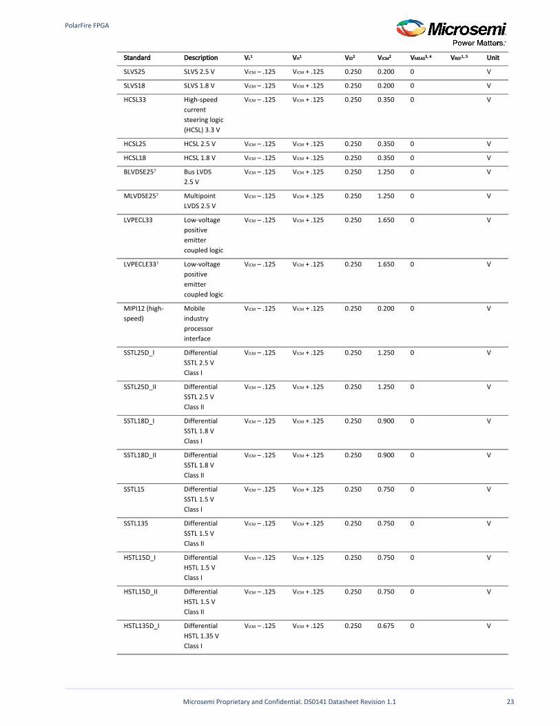
PolarFire FPGA
Microsemi Proprietary and Confidential. DS0141 Datasheet Revision 1.1 23
Standard Description VL1 VH1 VID2 VICM2 VMEAS3, 4 VREF1, 5 Unit
SLVS25 SLVS 2.5 V V – .125ICM V + .125ICM 0.250 0.200 0 V
SLVS18 SLVS 1.8 V V – .125ICM V + .125ICM 0.250 0.200 0 V
HCSL33 High-speed current steering logic (HCSL) 3.3 V
V – .125ICM V + .125ICM 0.250 0.350 0 V
HCSL25 HCSL 2.5 V V – .125ICM V + .125ICM 0.250 0.350 0 V
HCSL18 HCSL 1.8 V V – .125ICM V + .125ICM 0.250 0.350 0 V
BLVDSE257 Bus LVDS2.5 V
V – .125ICM V + .125ICM 0.250 1.250 0 V
MLVDSE257 Multipoint LVDS 2.5 V
V – .125ICM V + .125ICM 0.250 1.250 0 V
LVPECL33 Low-voltage positive emitter coupled logic
V – .125ICM V + .125ICM 0.250 1.650 0 V
LVPECLE337 Low-voltage positive emitter coupled logic
V – .125ICM V + .125ICM 0.250 1.650 0 V
MIPI12 (high- speed)
Mobile industry processor interface
V – .125ICM V + .125ICM 0.250 0.200 0 V
SSTL25D_I Differential SSTL 2.5 V Class I
V – .125ICM V + .125ICM 0.250 1.250 0 V
SSTL25D_II Differential SSTL 2.5 V Class II
V – .125ICM V + .125ICM 0.250 1.250 0 V
SSTL18D_I Differential SSTL 1.8 V Class I
V – .125ICM V + .125ICM 0.250 0.900 0 V
SSTL18D_II Differential SSTL 1.8 V Class II
V – .125ICM V + .125ICM 0.250 0.900 0 V
SSTL15 Differential SSTL 1.5 V Class I
V – .125ICM V + .125ICM 0.250 0.750 0 V
SSTL135 Differential SSTL 1.5 V Class II
V – .125ICM V + .125ICM 0.250 0.750 0 V
HSTL15D_I Differential HSTL 1.5 V Class I
V – .125ICM V + .125ICM 0.250 0.750 0 V
HSTL15D_II Differential HSTL 1.5 V Class II
V – .125ICM V + .125ICM 0.250 0.750 0 V
HSTL135D_I Differential HSTL 1.35 V Class I
V – .125ICM V + .125ICM 0.250 0.675 0 V
PolarFire FPGA
Microsemi Proprietary and Confidential. DS0141 Datasheet Revision 1.1 24
1.
2.
3. 4. 5.
6. 7.
Standard Description VL1 VH1 VID2 VICM2 VMEAS3, 4 VREF1, 5 Unit
HSTL135D_II Differential HSTL 1.35 V Class II
V – .125ICM V + .125ICM 0.250 0.675 0 V
HSTL12 Differential HSTL 1.2 V
V – .125ICM V + .125ICM 0.250 0.600 0 V
HSUL18D_I Differential HSUL 1.8 V Class I
V – .125ICM V + .125ICM 0.250 0.900 0 V
HSUL18D_II Differential HSUL 1.8 V Class II
V – .125ICM V + .125ICM 0.250 0.900 0 V
HSUL12 Differential HSUL 1.2 V
V – .125ICM V + .125ICM 0.250 0.600 0 V
POD12D_I Differential POD 1.2 V Class I
V – .125ICM V + .125ICM 0.250 0.600 0 V
POD12D_II Differential POD 1.2 V Class II
V – .125ICM V + .125ICM 0.250 0.600 0 V
LVSTLD_I Differential LVSTL 1.1 V Class I
V – .125ICM V + .125ICM 0.250 0.550 0 V
LVSTLD_II Differential LVSTL 1.1 V Class II
V – .125ICM V + .125ICM 0.250 0.550 0 V
Measurements are made at typical, minimum, and maximum V values. Reported delays reflect REF
worst-case of these measurements. V values listed are typical. Input waveform switches between REF
V and V . All rise and fall times must be 1 V/ns.L H
Differential receiver standards all use 250 mV V for timing. V is different between different ID CM
standards.Input voltage level from which measurement starts.The value given is the differential input voltage.This is an input voltage reference that bears no relation to the V /V parameters found in IBIS REF MEAS
models or shown in .Output Delay Measurement—Single-Ended Test Setup (see page 26)V cannot exceed 0.95 V.ICM
Emulated bi-directional interface.
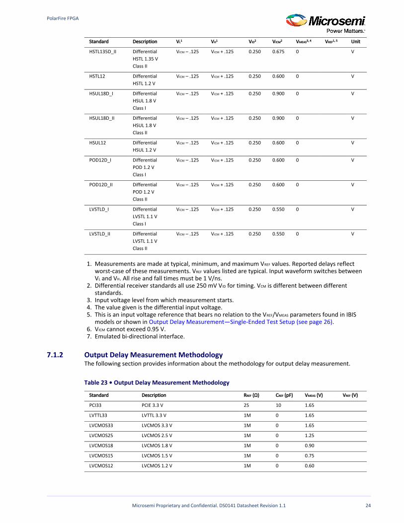
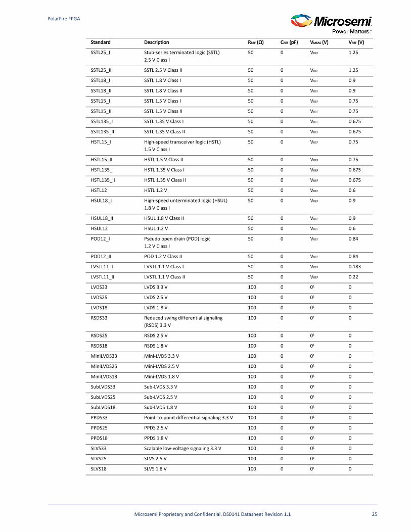
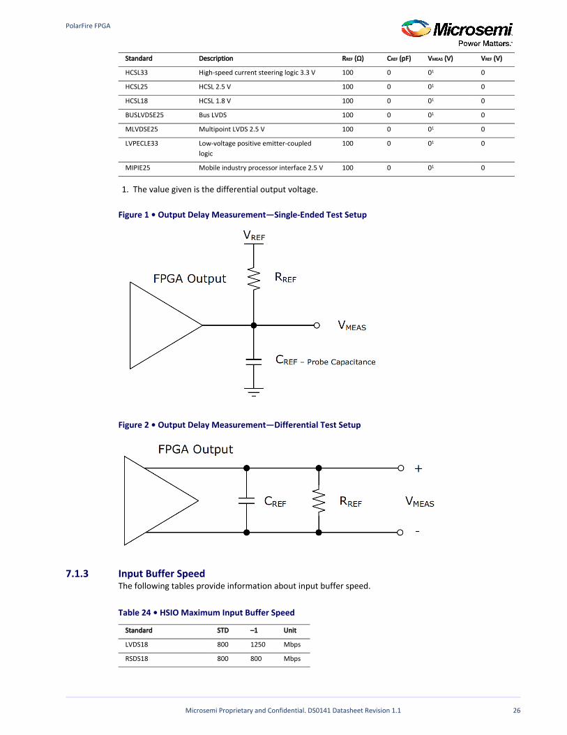
7.1.2 Output Delay Measurement MethodologyThe following section provides information about the methodology for output delay measurement.
Table 23 • Output Delay Measurement Methodology
Standard Description R (Ω)REF C (pF)REF V (V)MEAS V (V)REF
PCI33 PCIE 3.3 V 25 10 1.65
LVTTL33 LVTTL 3.3 V 1M 0 1.65
LVCMOS33 LVCMOS 3.3 V 1M 0 1.65
LVCMOS25 LVCMOS 2.5 V 1M 0 1.25
LVCMOS18 LVCMOS 1.8 V 1M 0 0.90
LVCMOS15 LVCMOS 1.5 V 1M 0 0.75
LVCMOS12 LVCMOS 1.2 V 1M 0 0.60
PolarFire FPGA
Microsemi Proprietary and Confidential. DS0141 Datasheet Revision 1.1 25
Standard Description R (Ω)REF C (pF)REF V (V)MEAS V (V)REF
SSTL25_I Stub-series terminated logic (SSTL)2.5 V Class I
50 0 VREF 1.25
SSTL25_II SSTL 2.5 V Class II 50 0 VREF 1.25
SSTL18_I SSTL 1.8 V Class I 50 0 VREF 0.9
SSTL18_II SSTL 1.8 V Class II 50 0 VREF 0.9
SSTL15_I SSTL 1.5 V Class I 50 0 VREF 0.75
SSTL15_II SSTL 1.5 V Class II 50 0 VREF 0.75
SSTL135_I SSTL 1.35 V Class I 50 0 VREF 0.675
SSTL135_II SSTL 1.35 V Class II 50 0 VREF 0.675
HSTL15_I High-speed transceiver logic (HSTL)1.5 V Class I
50 0 VREF 0.75
HSTL15_II HSTL 1.5 V Class II 50 0 VREF 0.75
HSTL135_I HSTL 1.35 V Class I 50 0 VREF 0.675
HSTL135_II HSTL 1.35 V Class II 50 0 VREF 0.675
HSTL12 HSTL 1.2 V 50 0 VREF 0.6
HSUL18_I High-speed unterminated logic (HSUL)1.8 V Class I
50 0 VREF 0.9
HSUL18_II HSUL 1.8 V Class II 50 0 VREF 0.9
HSUL12 HSUL 1.2 V 50 0 VREF 0.6
POD12_I Pseudo open drain (POD) logic1.2 V Class I
50 0 VREF 0.84
POD12_II POD 1.2 V Class II 50 0 VREF 0.84
LVSTL11_I LVSTL 1.1 V Class I 50 0 VREF 0.183
LVSTL11_II LVSTL 1.1 V Class II 50 0 VREF 0.22
LVDS33 LVDS 3.3 V 100 0 01 0
LVDS25 LVDS 2.5 V 100 0 01 0
LVDS18 LVDS 1.8 V 100 0 01 0
RSDS33 Reduced swing differential signaling (RSDS) 3.3 V
100 0 01 0
RSDS25 RSDS 2.5 V 100 0 01 0
RSDS18 RSDS 1.8 V 100 0 01 0
MiniLVDS33 Mini-LVDS 3.3 V 100 0 01 0
MiniLVDS25 Mini-LVDS 2.5 V 100 0 01 0
MiniLVDS18 Mini-LVDS 1.8 V 100 0 01 0
SubLVDS33 Sub-LVDS 3.3 V 100 0 01 0
SubLVDS25 Sub-LVDS 2.5 V 100 0 01 0
SubLVDS18 Sub-LVDS 1.8 V 100 0 01 0
PPDS33 Point-to-point differential signaling 3.3 V 100 0 01 0
PPDS25 PPDS 2.5 V 100 0 01 0
PPDS18 PPDS 1.8 V 100 0 01 0
SLVS33 Scalable low-voltage signaling 3.3 V 100 0 01 0
SLVS25 SLVS 2.5 V 100 0 01 0
SLVS18 SLVS 1.8 V 100 0 01 0
PolarFire FPGA
Microsemi Proprietary and Confidential. DS0141 Datasheet Revision 1.1 26
1.
Standard Description R (Ω)REF C (pF)REF V (V)MEAS V (V)REF
HCSL33 High-speed current steering logic 3.3 V 100 0 01 0
HCSL25 HCSL 2.5 V 100 0 01 0
HCSL18 HCSL 1.8 V 100 0 01 0
BUSLVDSE25 Bus LVDS 100 0 01 0
MLVDSE25 Multipoint LVDS 2.5 V 100 0 01 0
LVPECLE33 Low-voltage positive emitter-coupled logic
100 0 01 0
MIPIE25 Mobile industry processor interface 2.5 V 100 0 01 0
The value given is the differential output voltage.
Figure 1 • Output Delay Measurement—Single-Ended Test Setup
Figure 2 • Output Delay Measurement—Differential Test Setup
7.1.3 Input Buffer SpeedThe following tables provide information about input buffer speed.
Table 24 • HSIO Maximum Input Buffer Speed
Standard STD –1 Unit
LVDS18 800 1250 Mbps
RSDS18 800 800 Mbps
PolarFire FPGA
Microsemi Proprietary and Confidential. DS0141 Datasheet Revision 1.1 27
Standard STD –1 Unit
MiniLVDS18 800 800 Mbps
SUBLVDS18 800 800 Mbps
PPDS18 800 800 Mbps
SLVS18 800 800 Mbps
SSTL18_I 800 1066 Mbps
SSTL18_II 800 1066 Mbps
SSTL15_I 1066 1333 Mbps
SSTL15_II 1066 1333 Mbps
SSTL135_I 1066 1333 Mbps
SSTL135_II 1066 1333 Mbps
HSTL15_I 900 1100 Mbps
HSTL15_II 900 1100 Mbps
HSTL135_I 1066 1066 Mbps
HSTL135_II 1066 1066 Mbps
HSUL18_I 400 400 Mbps
HSUL18_II 400 400 Mbps
HSUL12 1066 1333 Mbps
HSTL12 1066 1266 Mbps
POD12_I 1333 1600 Mbps
POD12_II 1333 1600 Mbps
LVSTL11_I 1333 1600 Mbps
LVSTL11_II 1333 1600 Mbps
LVCMOS18 (12 mA) 500 500 Mbps
LVCMOS15 (10 mA) 500 500 Mbps
LVCMOS12 (8 mA) 300 300 Mbps
Table 25 • GPIO Maximum Input Buffer Speed
Standard STD –1 Unit
LVDS25/LVDS33 800 1250 Mbps
RSDS25/RSDS33 800 800 Mbps
MINILVDS25/MINILVDS33 800 800 Mbps
SUBLVDS25/SUBLVDS33 800 800 Mbps
PPDS25/PPDS33 800 800 Mbps
SLVS25/SLVS33 800 800 Mbps
SLVSE15 800 800 Mbps
HCSL25/HCSL33 800 800 Mbps
BUSLVDSE25 800 800 Mbps
MLVDSE25 800 800 Mbps
LVPECL33 800 800 Mbps
MIPI25/MIPI33 800 800 Mbps
SSTL25_I 800 800 Mbps
SSTL25_II 800 800 Mbps
PolarFire FPGA
Microsemi Proprietary and Confidential. DS0141 Datasheet Revision 1.1 28
Standard STD –1 Unit
SSTL18_I 800 800 Mbps
SSTL18_II 800 800 Mbps
SSTL15_I 800 1066 Mbps
SSTL15_II 800 1066 Mbps
HSTL15_I 900 900 Mbps
HSTL15_II 900 900 Mbps
HSUL18_I 400 400 Mbps
HSUL18_II 400 400 Mbps
PCI33 500 500 Mbps
LVTTL33 (20 mA) 500 500 Mbps
LVCMOS33 (20 mA) 500 500 Mbps
LVCMOS25 (16 mA) 500 500 Mbps
LVCMOS18 (12 mA) 500 500 Mbps
LVCMOS15 (10 mA) 500 500 Mbps
LVCMOS12 (8 mA) 300 300 Mbps
Note: All SSTLD/HSTLD/HSULD/LVSTLD/PODD type receivers use the LVDS differential receiver.
7.1.4 Output Buffer SpeedThe following tables provide information about output buffer speed.
Table 26 • HSIO Maximum Output Buffer Speed
Standard STD –1 Unit
SSTL18_I 800 1066 Mbps
SSTL18_II 800 1066 Mbps
SSTL18D_I 800 1066 Mbps
SSTL18D_II 800 1066 Mbps
SSTL15_I 1066 1333 Mbps
SSTL15_II 1066 1333 Mbps
SSTL15D_I 1066 1333 Mbps
SSTL15D_II 1066 1333 Mbps
SSTL135_I 1066 1333 Mbps
SSTL135_II 1066 1333 Mbps
SSTL135D_I 1066 1333 Mbps
SSTL135D_II 1066 1333 Mbps
HSTL15_I 900 1100 Mbps
HSTL15_II 900 1100 Mbps
HSTL15D_I 900 1100 Mbps
HSTL15D_II 900 1100 Mbps
HSTL135_I 1066 1066 Mbps
HSTL135_II 1066 1066 Mbps
HSTL135D_I 1066 1066 Mbps
HSTL135D_II 1066 1066 Mbps
PolarFire FPGA
Microsemi Proprietary and Confidential. DS0141 Datasheet Revision 1.1 29
Standard STD –1 Unit
HSUL18_I 400 400 Mbps
HSUL18_II 400 400 Mbps
HSUL18D_II 400 400 Mbps
HSUL12 1066 1333 Mbps
HSUL12D_I 1066 1333 Mbps
HSTL12 1066 1266 Mbps
HSTL12D_I 1066 1266 Mbps
POD12_I 1333 1600 Mbps
POD12_II 1333 1600 Mbps
LVSTL11_I 1333 1600 Mbps
LVSTL11_II 1333 1600 Mbps
LVCMOS18 (12 mA) 500 500 Mbps
LVCMOS15 (10 mA) 500 500 Mbps
LVCMOS12 (8 mA) 250 300 Mbps
Table 27 • GPIO Maximum Output Buffer Speed
Standard STD –1 Unit
LVDS25 800 1250 Mbps
RSDS25 800 800 Mbps
MINILVDS25 800 800 Mbps
SUBLVDS25 800 800 Mbps
PPDS25 800 800 Mbps
SLVSE15 500 500 Mbps
BUSLVDSE25 500 500 Mbps
MLVDSE25 500 500 Mbps
LVPECLE33 500 500 Mbps
MIPIE25 500 500 Mbps
SSTL25_I 800 800 Mbps
SSTL25_II 800 800 Mbps
SSTL25D_I 800 800 Mbps
SSTL25D_II 800 800 Mbps
SSTL18_I 800 800 Mbps
SSTL18_II 800 800 Mbps
SSTL18D_I 800 800 Mbps
SSTL18D_II 800 800 Mbps
SSTL15_I 800 1066 Mbps
SSTL15_II 800 1066 Mbps
SSTL15D_I 800 1066 Mbps
SSTL15D_II 800 1066 Mbps
HSTL15_I 900 900 Mbps
HSTL15_II 900 900 Mbps
HSTL15D_I 900 900 Mbps
PolarFire FPGA
Microsemi Proprietary and Confidential. DS0141 Datasheet Revision 1.1 30
1.
2.
Standard STD –1 Unit
HSTL15D_II 900 900 Mbps
HSUL18_I 400 400 Mbps
HSUL18_II 400 400 Mbps
HSUL18D_I 400 400 Mbps
HSUL18D_II 400 400 Mbps
PCI33 500 500 Mbps
LVTTL33 (20 mA) 500 500 Mbps
LVCMOS33 (20 mA) 500 500 Mbps
LVCMOS25 (16 mA) 500 500 Mbps
LVCMOS18 (12 mA) 500 500 Mbps
LVCMOS15 (10 mA) 500 500 Mbps
LVCMOS12 (8 mA) 250 300 Mbps
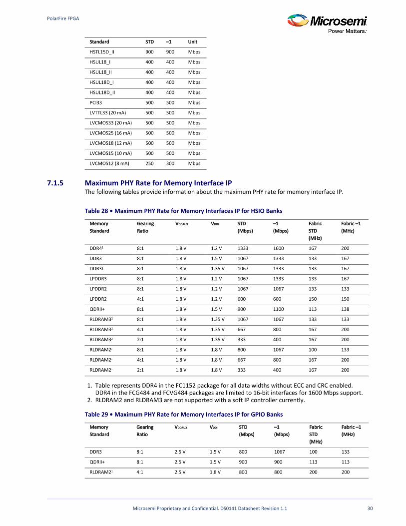
7.1.5 Maximum PHY Rate for Memory Interface IPThe following tables provide information about the maximum PHY rate for memory interface IP.
Table 28 • Maximum PHY Rate for Memory Interfaces IP for HSIO Banks
Memory Standard
Gearing Ratio
VDDAUX VDDI STD(Mbps)
–1(Mbps)
Fabric STD (MHz)
–1 Fabric (MHz)
DDR41 8:1 1.8 V 1.2 V 1333 1600 167 200
DDR3 8:1 1.8 V 1.5 V 1067 1333 133 167
DDR3L 8:1 1.8 V 1.35 V 1067 1333 133 167
LPDDR3 8:1 1.8 V 1.2 V 1067 1333 133 167
LPDDR2 8:1 1.8 V 1.2 V 1067 1067 133 133
LPDDR2 4:1 1.8 V 1.2 V 600 600 150 150
QDRII+ 8:1 1.8 V 1.5 V 900 1100 113 138
RLDRAM32 8:1 1.8 V 1.35 V 1067 1067 133 133
RLDRAM32 4:1 1.8 V 1.35 V 667 800 167 200
RLDRAM32 2:1 1.8 V 1.35 V 333 400 167 200
RLDRAM22 8:1 1.8 V 1.8 V 800 1067 100 133
RLDRAM22 4:1 1.8 V 1.8 V 667 800 167 200
RLDRAM22 2:1 1.8 V 1.8 V 333 400 167 200
Table represents DDR4 in the FC1152 package for all data widths without ECC and CRC enabled. DDR4 in the FCG484 and FCVG484 packages are limited to 16-bit interfaces for 1600 Mbps support.RLDRAM2 and RLDRAM3 are not supported with a soft IP controller currently.
Table 29 • Maximum PHY Rate for Memory Interfaces IP for GPIO Banks
Memory Standard
Gearing Ratio
VDDAUX VDDI STD(Mbps)
–1(Mbps)
Fabric STD (MHz)
Fabric –1 (MHz)
DDR3 8:1 2.5 V 1.5 V 800 1067 100 133
QDRII+ 8:1 2.5 V 1.5 V 900 900 113 113
RLDRAM21 4:1 2.5 V 1.8 V 800 800 200 200
PolarFire FPGA
Microsemi Proprietary and Confidential. DS0141 Datasheet Revision 1.1 31
1.
1.
Memory Standard
Gearing Ratio
VDDAUX VDDI STD(Mbps)
–1(Mbps)
Fabric STD (MHz)
Fabric –1 (MHz)
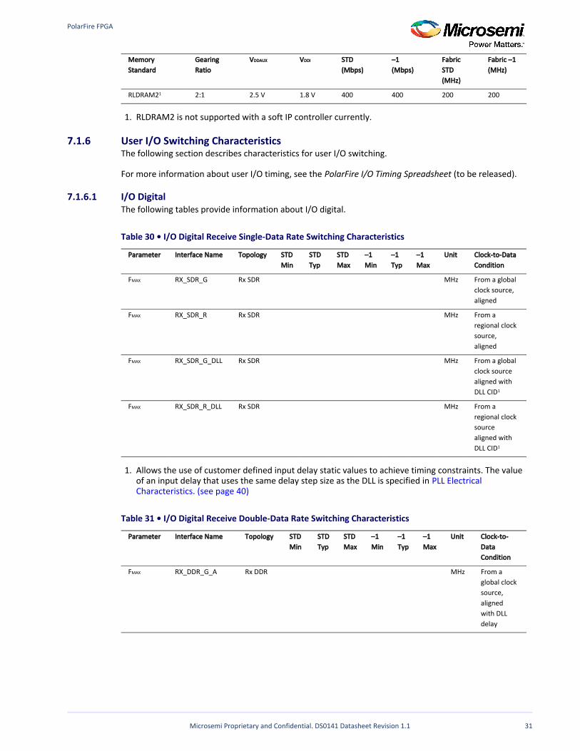
RLDRAM21 2:1 2.5 V 1.8 V 400 400 200 200
RLDRAM2 is not supported with a soft IP controller currently.
7.1.6 User I/O Switching CharacteristicsThe following section describes characteristics for user I/O switching.
For more information about user I/O timing, see the (to be released).PolarFire I/O Timing Spreadsheet
7.1.6.1 I/O DigitalThe following tables provide information about I/O digital.
Table 30 • I/O Digital Receive Single-Data Rate Switching Characteristics
Parameter Interface Name Topology STD Min
STD Typ
STD Max
–1Min
–1Typ
–1Max
Unit Clock-to-Data Condition
FMAX RX_SDR_G Rx SDR MHz From a global clock source, aligned
FMAX RX_SDR_R Rx SDR MHz From a regional clock source, aligned
FMAX RX_SDR_G_DLL Rx SDR MHz From a global clock source aligned with DLL CID1
FMAX RX_SDR_R_DLL Rx SDR MHz From a regional clock source aligned with DLL CID1
Allows the use of customer defined input delay static values to achieve timing constraints. The value of an input delay that uses the same delay step size as the DLL is specified in PLL Electrical Characteristics. (see page 40)
Table 31 • I/O Digital Receive Double-Data Rate Switching Characteristics
Parameter Interface Name Topology STD Min
STDTyp
STDMax
–1Min
–1Typ
–1Max
Unit Clock-to-Data Condition
FMAX RX_DDR_G_A Rx DDR MHz From a global clock source, aligned with DLL delay
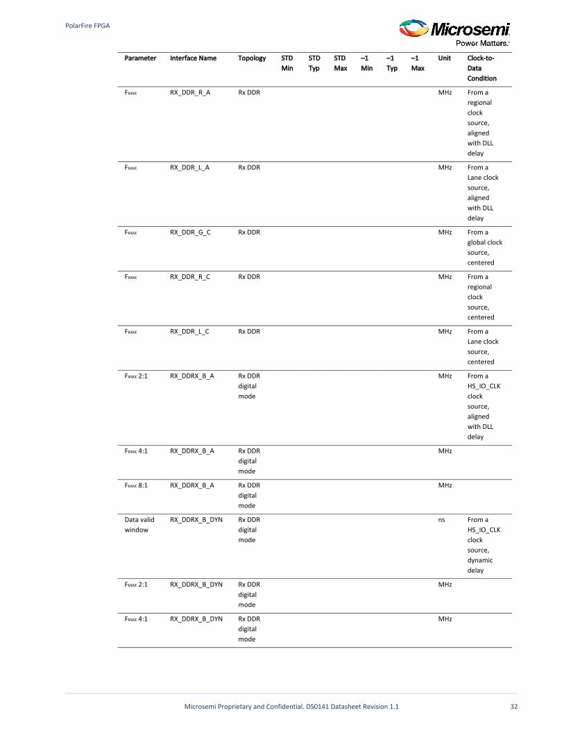
PolarFire FPGA
Microsemi Proprietary and Confidential. DS0141 Datasheet Revision 1.1 32
Parameter Interface Name Topology STD Min
STDTyp
STDMax
–1Min
–1Typ
–1Max
Unit Clock-to-Data Condition
FMAX RX_DDR_R_A Rx DDR MHz From a regional clock source, aligned with DLL delay
FMAX RX_DDR_L_A Rx DDR MHz From a Lane clock source, aligned with DLL delay
FMAX RX_DDR_G_C Rx DDR MHz From a global clock source, centered
FMAX RX_DDR_R_C Rx DDR MHz From a regional clock source, centered
FMAX RX_DDR_L_C Rx DDR MHz From a Lane clock source, centered
F 2:1MAX RX_DDRX_B_A Rx DDR digital mode
MHz From a HS_IO_CLK clock source, aligned with DLL delay
F 4:1MAX RX_DDRX_B_A Rx DDR digital mode
MHz
F 8:1MAX RX_DDRX_B_A Rx DDR digital mode
MHz
Data valid window
RX_DDRX_B_DYN Rx DDR digital mode
ns From a HS_IO_CLK clock source, dynamic delay
F 2:1MAX RX_DDRX_B_DYN Rx DDR digital mode
MHz
F 4:1MAX RX_DDRX_B_DYN Rx DDR digital mode
MHz
PolarFire FPGA
Microsemi Proprietary and Confidential. DS0141 Datasheet Revision 1.1 33
1.
Parameter Interface Name Topology STD Min
STDTyp
STDMax
–1Min
–1Typ
–1Max
Unit Clock-to-Data Condition
F 8:1MAX RX_DDRX_B_DYN Rx DDR digital mode
MHz
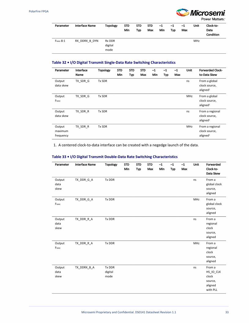
Table 32 • I/O Digital Transmit Single-Data Rate Switching Characteristics
Parameter Interface Name
Topology STD Min
STDTyp
STDMax
–1Min
–1Typ
–1Max
Unit Forwarded Clock-to-Data Skew
Output data skew
TX_SDR_G Tx SDR ns From a global clock source, aligned1
OutputFMAX
TX_SDR_G Tx SDR MHz From a global clock source, aligned1
Output data skew
TX_SDR_R Tx SDR ns From a regional clock source, aligned1
Output maximum frequency
TX_SDR_R Tx SDR MHz From a regional clock source, aligned1
A centered clock-to-data interface can be created with a negedge launch of the data.
Table 33 • I/O Digital Transmit Double-Data Rate Switching Characteristics
Parameter Interface Name Topology STD Min
STDTyp
STDMax
–1Min
–1Typ
–1Max
Unit Forwarded Clock-to-Data Skew
Output data skew
TX_DDR_G_A Tx DDR ns From a global clock source, aligned
OutputFMAX
TX_DDR_G_A Tx DDR MHz From a global clock source, aligned
Output data skew
TX_DDR_R_A Tx DDR ns From a regional clock source, aligned
OutputFMAX
TX_DDR_R_A Tx DDR MHz From a regional clock source, aligned
Output data skew
TX_DDRX_B_A Tx DDRdigital mode
ns From a HS_IO_CLK clock source, aligned with PLL
PolarFire FPGA
Microsemi Proprietary and Confidential. DS0141 Datasheet Revision 1.1 34
Parameter Interface Name Topology STD Min
STDTyp
STDMax
–1Min
–1Typ
–1Max
Unit Forwarded Clock-to-Data Skew
OutputF 2:1MAX
TX_DDRX_B_A Tx DDR digital mode
MHz From a HS_IO_CLK clock source, aligned with PLL
OutputF 4:1MAX
TX_DDRX_B_A Tx DDR digital mode
MHz From a HS_IO_CLK clock source, aligned with PLL
OutputF 8:1MAX
TX_DDRX_B_A Tx DDR digital mode
MHz From a HS_IO_CLK clock source, aligned with PLL
Output data skew
TX_DDRX_B_DYN Tx DDR digital mode
ns From a HS_IO_CLK clock source, dynamic with PLL
OutputF 2:1MAX
TX_DDRX_B_DYN Tx DDR digital mode
MHz From a HS_IO_CLK clock source, dynamic with PLL
OutputF 4:1MAX
TX_DDRX_B_DYN Tx DDR digital mode
MHz From a HS_IO_CLK clock source, dynamic with PLL
OutputF 8:1MAX
TX_DDRX_B_DYN Tx DDR digital mode
MHz From a HS_IO_CLK clock source, dynamic with PLL
In delay, out delay,DLL delay step sizes
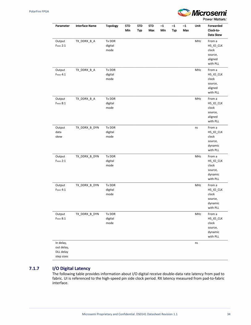
ns
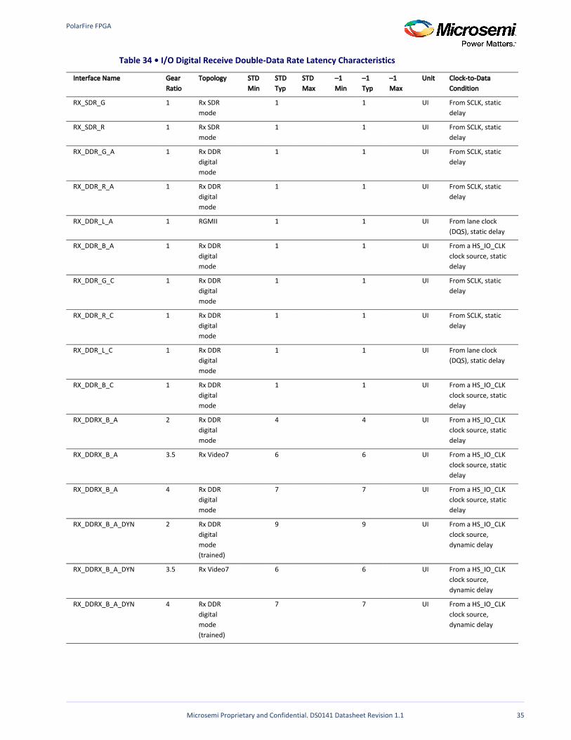
7.1.7 I/O Digital LatencyThe following table provides information about I/O digital receive double-data rate latency from pad to fabric. UI is referenced to the high-speed pin side clock period. RX latency measured from pad-to-fabric interface.
PolarFire FPGA
Microsemi Proprietary and Confidential. DS0141 Datasheet Revision 1.1 35
Table 34 • I/O Digital Receive Double-Data Rate Latency Characteristics
Interface Name Gear Ratio
Topology STDMin
STDTyp
STDMax
–1Min
–1Typ
–1Max
Unit Clock-to-Data Condition
RX_SDR_G 1 Rx SDR mode
1 1 UI From SCLK, static delay
RX_SDR_R 1 Rx SDR mode
1 1 UI From SCLK, static delay
RX_DDR_G_A 1 Rx DDR digital mode
1 1 UI From SCLK, static delay
RX_DDR_R_A 1 Rx DDR digital mode
1 1 UI From SCLK, static delay
RX_DDR_L_A 1 RGMII 1 1 UI From lane clock (DQS), static delay
RX_DDR_B_A 1 Rx DDR digital mode
1 1 UI From a HS_IO_CLK clock source, static delay
RX_DDR_G_C 1 Rx DDR digital mode
1 1 UI From SCLK, static delay
RX_DDR_R_C 1 Rx DDR digital mode
1 1 UI From SCLK, static delay
RX_DDR_L_C 1 Rx DDR digital mode
1 1 UI From lane clock (DQS), static delay
RX_DDR_B_C 1 Rx DDR digital mode
1 1 UI From a HS_IO_CLK clock source, static delay
RX_DDRX_B_A 2 Rx DDR digital mode
4 4 UI From a HS_IO_CLK clock source, static delay
RX_DDRX_B_A 3.5 Rx Video7 6 6 UI From a HS_IO_CLK clock source, static delay
RX_DDRX_B_A 4 Rx DDR digital mode
7 7 UI From a HS_IO_CLK clock source, static delay
RX_DDRX_B_A_DYN 2 Rx DDR digital mode (trained)
9 9 UI From a HS_IO_CLK clock source, dynamic delay
RX_DDRX_B_A_DYN 3.5 Rx Video7 6 6 UI From a HS_IO_CLK clock source, dynamic delay
RX_DDRX_B_A_DYN 4 Rx DDR digital mode (trained)
7 7 UI From a HS_IO_CLK clock source, dynamic delay
PolarFire FPGA
Microsemi Proprietary and Confidential. DS0141 Datasheet Revision 1.1 36
Interface Name Gear Ratio
Topology STDMin
STDTyp
STDMax
–1Min
–1Typ
–1Max
Unit Clock-to-Data Condition
IOD_CDR_TX 5 Rx SGMII 9 9 UI Clock recovered from data, lane clock, dynamic delay
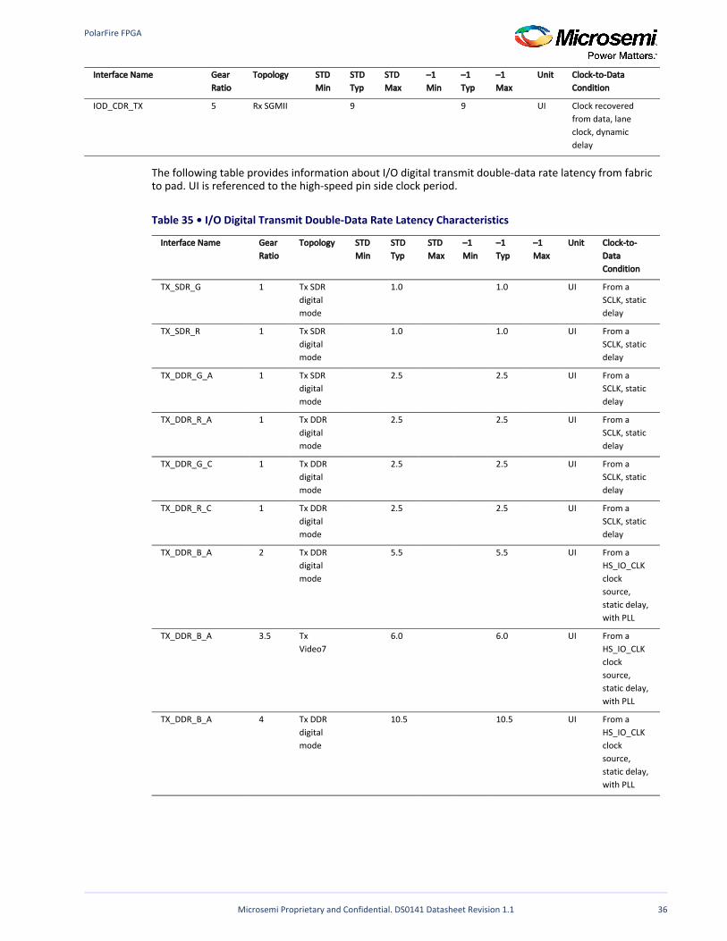
The following table provides information about I/O digital transmit double-data rate latency from fabric to pad. UI is referenced to the high-speed pin side clock period.
Table 35 • I/O Digital Transmit Double-Data Rate Latency Characteristics
Interface Name Gear Ratio
Topology STD Min
STDTyp
STDMax
–1Min
–1Typ
–1Max
Unit Clock-to-Data Condition
TX_SDR_G 1 Tx SDR digital mode
1.0 1.0 UI From a SCLK, static delay
TX_SDR_R 1 Tx SDR digital mode
1.0 1.0 UI From a SCLK, static delay
TX_DDR_G_A 1 Tx SDR digital mode
2.5 2.5 UI From a SCLK, static delay
TX_DDR_R_A 1 Tx DDR digital mode
2.5 2.5 UI From a SCLK, static delay
TX_DDR_G_C 1 Tx DDR digital mode
2.5 2.5 UI From a SCLK, static delay
TX_DDR_R_C 1 Tx DDR digital mode
2.5 2.5 UI From a SCLK, static delay
TX_DDR_B_A 2 Tx DDR digital mode
5.5 5.5 UI From a HS_IO_CLK clock source, static delay, with PLL
TX_DDR_B_A 3.5 Tx Video7
6.0 6.0 UI From a HS_IO_CLK clock source, static delay, with PLL
TX_DDR_B_A 4 Tx DDR digital mode
10.5 10.5 UI From a HS_IO_CLK clock source, static delay, with PLL
PolarFire FPGA
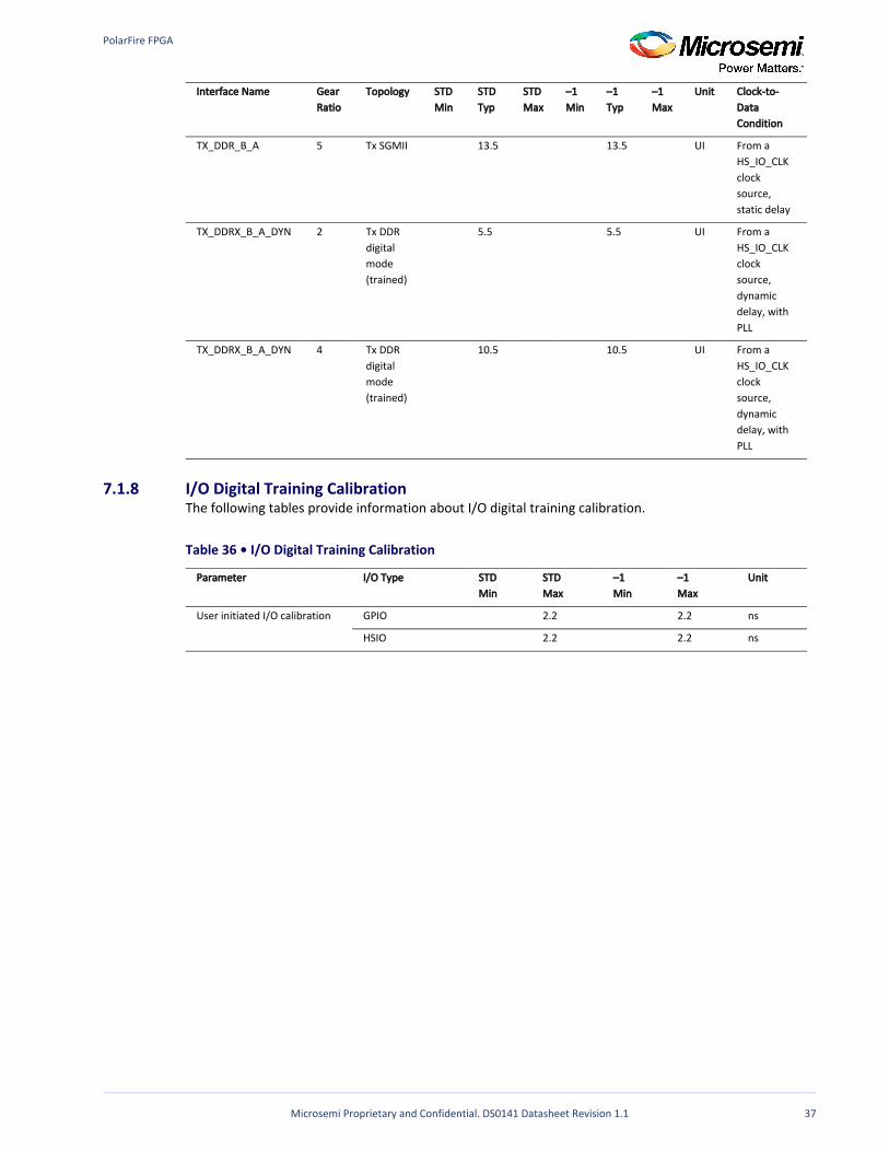
Microsemi Proprietary and Confidential. DS0141 Datasheet Revision 1.1 37
Interface Name Gear Ratio
Topology STD Min
STDTyp
STDMax
–1Min
–1Typ
–1Max
Unit Clock-to-Data Condition
TX_DDR_B_A 5 Tx SGMII 13.5 13.5 UI From a HS_IO_CLK clock source, static delay
TX_DDRX_B_A_DYN 2 Tx DDR digital mode (trained)
5.5 5.5 UI From a HS_IO_CLK clock source, dynamic delay, with PLL
TX_DDRX_B_A_DYN 4 Tx DDR digital mode (trained)
10.5 10.5 UI From a HS_IO_CLK clock source, dynamic delay, with PLL
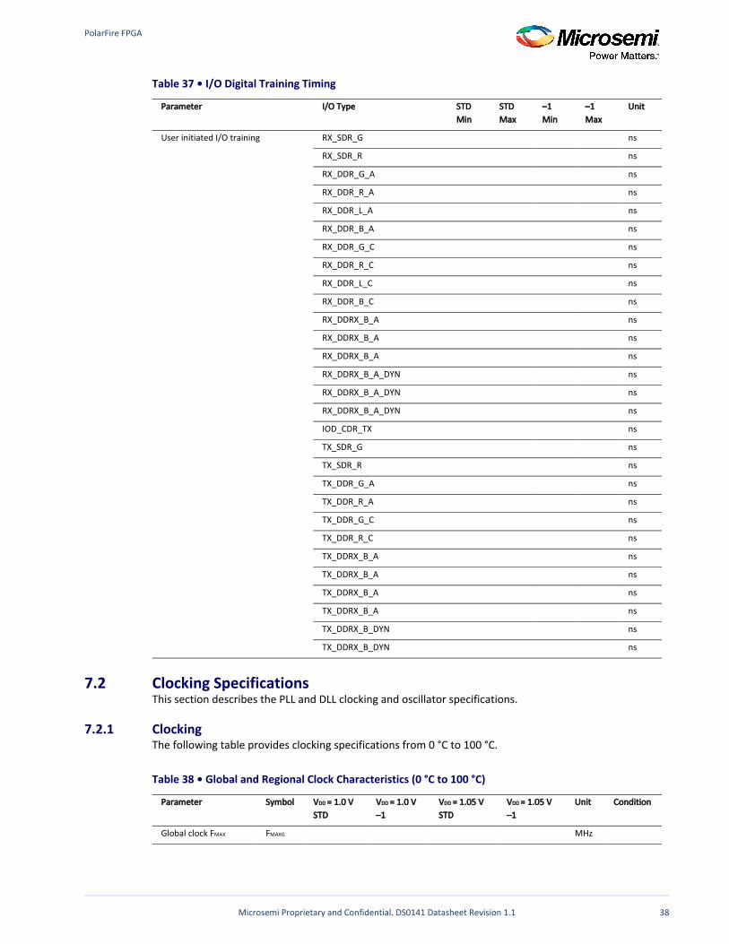
7.1.8 I/O Digital Training CalibrationThe following tables provide information about I/O digital training calibration.
Table 36 • I/O Digital Training Calibration
Parameter I/O Type STDMin
STDMax
–1Min
–1Max
Unit
User initiated I/O calibration GPIO 2.2 2.2 ns
HSIO 2.2 2.2 ns
PolarFire FPGA
Microsemi Proprietary and Confidential. DS0141 Datasheet Revision 1.1 38
Table 37 • I/O Digital Training Timing
Parameter I/O Type STD Min
STDMax
–1Min
–1Max
Unit
User initiated I/O training RX_SDR_G ns
RX_SDR_R ns
RX_DDR_G_A ns
RX_DDR_R_A ns
RX_DDR_L_A ns
RX_DDR_B_A ns
RX_DDR_G_C ns
RX_DDR_R_C ns
RX_DDR_L_C ns
RX_DDR_B_C ns
RX_DDRX_B_A ns
RX_DDRX_B_A ns
RX_DDRX_B_A ns
RX_DDRX_B_A_DYN ns
RX_DDRX_B_A_DYN ns
RX_DDRX_B_A_DYN ns
IOD_CDR_TX ns
TX_SDR_G ns
TX_SDR_R ns
TX_DDR_G_A ns
TX_DDR_R_A ns
TX_DDR_G_C ns
TX_DDR_R_C ns
TX_DDRX_B_A ns
TX_DDRX_B_A ns
TX_DDRX_B_A ns
TX_DDRX_B_A ns
TX_DDRX_B_DYN ns
TX_DDRX_B_DYN ns
7.2 Clocking SpecificationsThis section describes the PLL and DLL clocking and oscillator specifications.
7.2.1 ClockingThe following table provides clocking specifications from 0 °C to 100 °C.
Table 38 • Global and Regional Clock Characteristics (0 °C to 100 °C)
Parameter Symbol VDD = 1.0 VSTD
VDD = 1.0 V–1
VDD = 1.05 VSTD
VDD = 1.05 V–1
Unit Condition
Global clock FMAX FMAXG MHz
PolarFire FPGA
Microsemi Proprietary and Confidential. DS0141 Datasheet Revision 1.1 39
Parameter Symbol VDD = 1.0 VSTD
VDD = 1.0 V–1
VDD = 1.05 VSTD
VDD = 1.05 V–1
Unit Condition
Regional clock FMAX FMAXR MHz
Global clock skew FSKEWG ps
Regional clock skew FSKEWR ps
Global clock duty cycle distortion
TDCD ps
Regional clock duty cycle distortion
TDCD ps
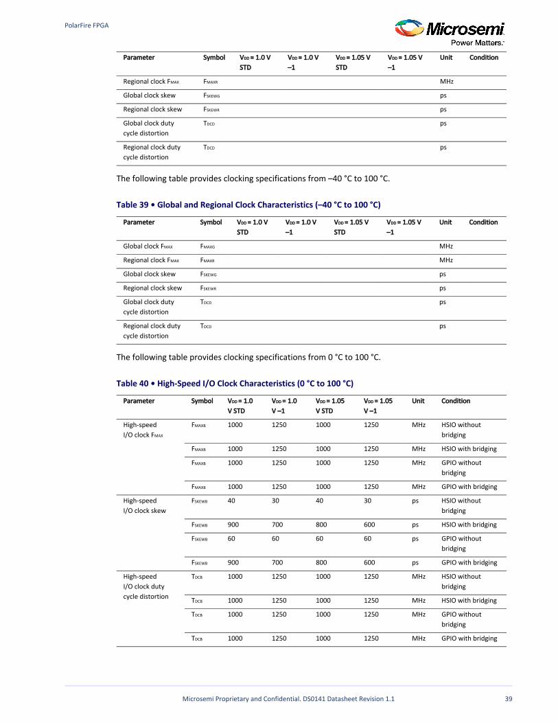
The following table provides clocking specifications from –40 °C to 100 °C.
Table 39 • Global and Regional Clock Characteristics (–40 °C to 100 °C)
Parameter Symbol VDD = 1.0 VSTD
VDD = 1.0 V–1
VDD = 1.05 VSTD
VDD = 1.05 V–1
Unit Condition
Global clock FMAX FMAXG MHz
Regional clock FMAX FMAXR MHz
Global clock skew FSKEWG ps
Regional clock skew FSKEWR ps
Global clock duty cycle distortion
TDCD ps
Regional clock duty cycle distortion
TDCD ps
The following table provides clocking specifications from 0 °C to 100 °C.
Table 40 • High-Speed I/O Clock Characteristics (0 °C to 100 °C)
Parameter Symbol V = 1.0 DD
V STDV = 1.0 DD
V –1V = 1.05 DD
V STDV = 1.05 DD
V –1Unit Condition
High-speedI/O clock FMAX
FMAXB 1000 1250 1000 1250 MHz HSIO without bridging
FMAXB 1000 1250 1000 1250 MHz HSIO with bridging
FMAXB 1000 1250 1000 1250 MHz GPIO without bridging
FMAXB 1000 1250 1000 1250 MHz GPIO with bridging
High-speedI/O clock skew
FSKEWB 40 30 40 30 ps HSIO without bridging
FSKEWB 900 700 800 600 ps HSIO with bridging
FSKEWB 60 60 60 60 ps GPIO without bridging
FSKEWB 900 700 800 600 ps GPIO with bridging
High-speedI/O clock duty cycle distortion
TDCB 1000 1250 1000 1250 MHz HSIO without bridging
TDCB 1000 1250 1000 1250 MHz HSIO with bridging
TDCB 1000 1250 1000 1250 MHz GPIO without bridging
TDCB 1000 1250 1000 1250 MHz GPIO with bridging
The following table provides clocking specifications from –40 °C to 100 °C.
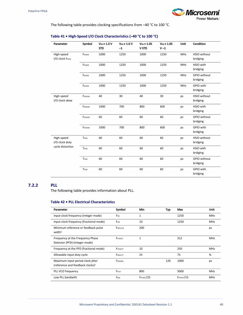
PolarFire FPGA
Microsemi Proprietary and Confidential. DS0141 Datasheet Revision 1.1 40
The following table provides clocking specifications from –40 °C to 100 °C.
Table 41 • High-Speed I/O Clock Characteristics (–40 °C to 100 °C)
Parameter Symbol V = 1.0 VDD
STD V = 1.0 VDD
–1V = 1.05 DD
STDVV = 1.05 DD
–1VUnit Condition
High-speedI/O clock FMAX
FMAXB 1000 1250 1000 1250 MHz HSIO without bridging
FMAXB 1000 1250 1000 1250 MHz HSIO with bridging
FMAXB 1000 1250 1000 1250 MHz GPIO without bridging
FMAXB 1000 1250 1000 1250 MHz GPIO with bridging
High-speedI/O clock skew
FSKEWB 40 30 40 30 ps HSIO without bridging
FSKEWB 1000 700 800 600 ps HSIO with bridging
FSKEWB 60 60 60 60 ps GPIO without bridging
FSKEWB 1000 700 800 600 ps GPIO with bridging
High-speedI/O clock duty cycle distortion
TDCB 60 60 60 60 ps HSIO without bridging
TDCB 60 60 60 60 ps HSIO with bridging
TDCB 60 60 60 60 ps GPIO without bridging
TDCB 60 60 60 60 ps GPIO with bridging
7.2.2 PLLThe following table provides information about PLL.
Table 42 • PLL Electrical Characteristics
Parameter Symbol Min Typ Max Unit
Input clock frequency (integer mode) FINI 1 1250 MHz
Input clock frequency (fractional mode) FINF 10 1250 MHz
Minimum reference or feedback pulse width1
FINPULSE 200 ps
Frequency at the Frequency Phase Detector (PFD) (integer mode)
FPHDETI 1 312 MHz
Frequency at the PFD (fractional mode) FPHDETF 10 250 MHz
Allowable input duty cycle FINDUTY 25 75 %
Maximum input period clock jitter (reference and feedback clocks)2
FMAXINJ 120 1000 ps
PLL VCO frequency FVCO 800 5000 MHz
Low PLL bandwith FBW F /25PHDET F /15PHDET MHz
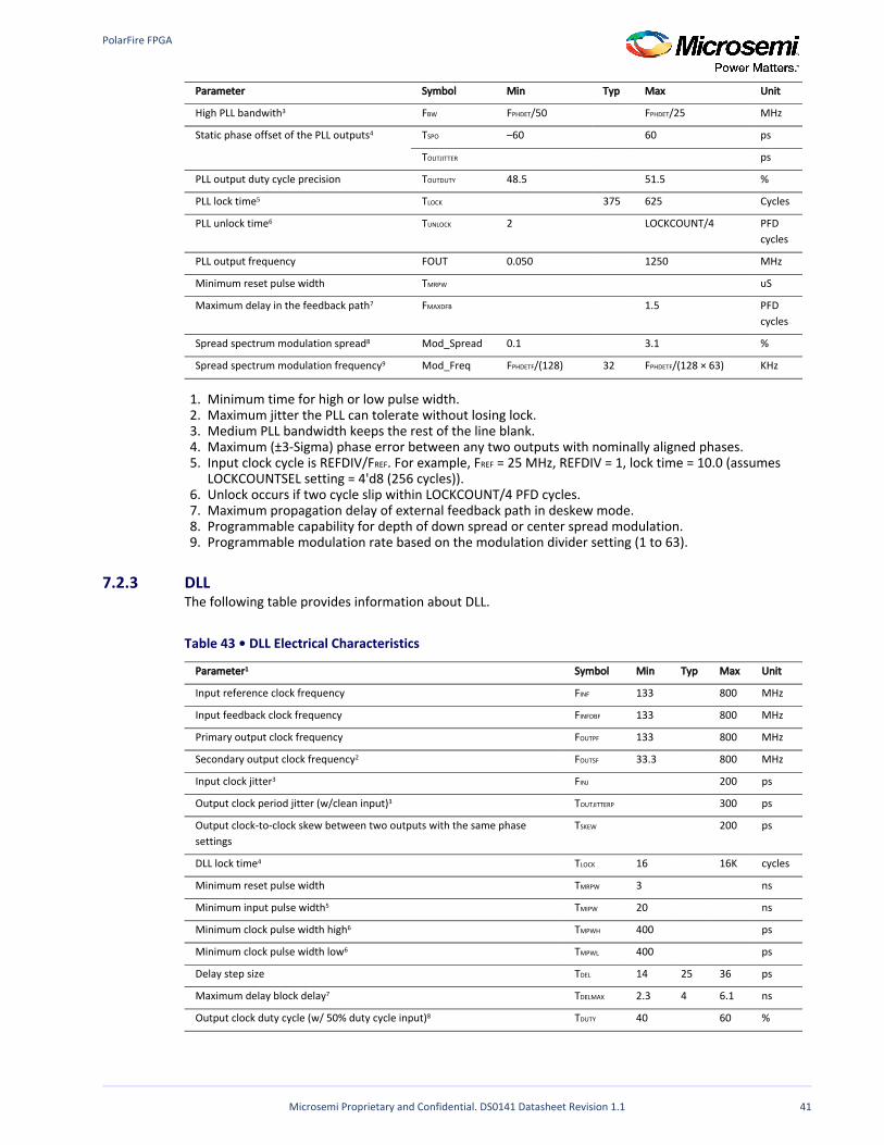
PolarFire FPGA
Microsemi Proprietary and Confidential. DS0141 Datasheet Revision 1.1 41
1. 2. 3. 4. 5.
6. 7. 8. 9.
Parameter Symbol Min Typ Max Unit
High PLL bandwith3 FBW F /50PHDET F /25PHDET MHz
Static phase offset of the PLL outputs4 TSPO –60 60 ps
TOUTJITTER ps
PLL output duty cycle precision TOUTDUTY 48.5 51.5 %
PLL lock time5 TLOCK 375 625 Cycles
PLL unlock time6 TUNLOCK 2 LOCKCOUNT/4 PFD cycles
PLL output frequency FOUT 0.050 1250 MHz
Minimum reset pulse width TMRPW uS
Maximum delay in the feedback path7 FMAXDFB 1.5 PFD cycles
Spread spectrum modulation spread8 Mod_Spread 0.1 3.1 %
Spread spectrum modulation frequency9 Mod_Freq F /(128)PHDETF 32 F /(128 × 63)PHDETF KHz
Minimum time for high or low pulse width.Maximum jitter the PLL can tolerate without losing lock.Medium PLL bandwidth keeps the rest of the line blank.Maximum (±3-Sigma) phase error between any two outputs with nominally aligned phases.Input clock cycle is REFDIV/F . For example, F = 25 MHz, REFDIV = 1, lock time = 10.0 (assumes REF REF
LOCKCOUNTSEL setting = 4'd8 (256 cycles)).Unlock occurs if two cycle slip within LOCKCOUNT/4 PFD cycles.Maximum propagation delay of external feedback path in deskew mode.Programmable capability for depth of down spread or center spread modulation.Programmable modulation rate based on the modulation divider setting (1 to 63).
7.2.3 DLLThe following table provides information about DLL.
Table 43 • DLL Electrical Characteristics
Parameter1 Symbol Min Typ Max Unit
Input reference clock frequency FINF 133 800 MHz
Input feedback clock frequency FINFDBF 133 800 MHz
Primary output clock frequency FOUTPF 133 800 MHz
Secondary output clock frequency2 FOUTSF 33.3 800 MHz
Input clock jitter3 FINJ 200 ps
Output clock period jitter (w/clean input)3 TOUTJITTERP 300 ps
Output clock-to-clock skew between two outputs with the same phase settings
TSKEW 200 ps
DLL lock time4 TLOCK 16 16K cycles
Minimum reset pulse width TMRPW 3 ns
Minimum input pulse width5 TMIPW 20 ns
Minimum clock pulse width high6 TMPWH 400 ps
Minimum clock pulse width low6 TMPWL 400 ps
Delay step size TDEL 14 25 36 ps
Maximum delay block delay7 TDELMAX 2.3 4 6.1 ns
Output clock duty cycle (w/ 50% duty cycle input)8 TDUTY 40 60 %
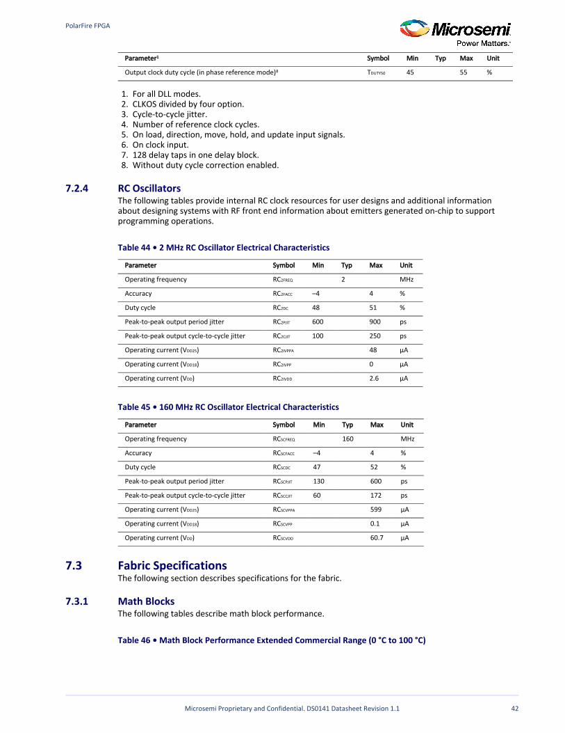
PolarFire FPGA
Microsemi Proprietary and Confidential. DS0141 Datasheet Revision 1.1 42
1. 2. 3. 4. 5. 6. 7. 8.
Parameter1 Symbol Min Typ Max Unit
Output clock duty cycle (in phase reference mode)8 TDUTY50 45 55 %
For all DLL modes.CLKOS divided by four option.Cycle-to-cycle jitter.Number of reference clock cycles.On load, direction, move, hold, and update input signals.On clock input.128 delay taps in one delay block.Without duty cycle correction enabled.
7.2.4 RC OscillatorsThe following tables provide internal RC clock resources for user designs and additional information about designing systems with RF front end information about emitters generated on-chip to support programming operations.
Table 44 • 2 MHz RC Oscillator Electrical Characteristics
Parameter Symbol Min Typ Max Unit
Operating frequency RC2FREQ 2 MHz
Accuracy RC2FACC –4 4 %
Duty cycle RC2DC 48 51 %
Peak-to-peak output period jitter RC2PJIT 600 900 ps
Peak-to-peak output cycle-to-cycle jitter RC2CJIT 100 250 ps
Operating current (V )DD25 RC2IVPPA 48 µA
Operating current (V )DD18 RC2IVPP 0 µA
Operating current (V )DD RC2IVDD 2.6 µA
Table 45 • 160 MHz RC Oscillator Electrical Characteristics
Parameter Symbol Min Typ Max Unit
Operating frequency RCSCFREQ 160 MHz
Accuracy RCSCFACC –4 4 %
Duty cycle RCSCDC 47 52 %
Peak-to-peak output period jitter RCSCPJIT 130 600 ps
Peak-to-peak output cycle-to-cycle jitter RCSCCJIT 60 172 ps
Operating current (V )DD25 RCSCVPPA 599 µA
Operating current (V )DD18 RCSCVPP 0.1 µA
Operating current (V )DD RCSCVDD 60.7 µA
7.3 Fabric SpecificationsThe following section describes specifications for the fabric.
7.3.1 Math BlocksThe following tables describe math block performance.
Table 46 • Math Block Performance Extended Commercial Range (0 °C to 100 °C)
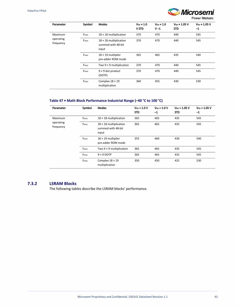
PolarFire FPGA
Microsemi Proprietary and Confidential. DS0141 Datasheet Revision 1.1 43
Parameter Symbol Modes V = 1.0 DD
STDVV = 1.0 DD
–1V V = 1.05 VDD
STD V = 1.05 VDD
–1
Maximum operating frequency
FMAX 18 × 18 multiplication 370 470 440 545
FMAX 18 × 18 multiplication summed with 48-bit input
370 470 440 545
FMAX 18 × 19 multiplierpre-adder ROM mode
365 465 435 540
FMAX Two 9 × 9 multiplication 370 470 440 545
FMAX 9 × 9 dot product (DOTP)
370 470 440 545
FMAX Complex 18 × 19 multiplication
360 455 430 530
Table 47 • Math Block Performance Industrial Range (–40 °C to 100 °C)
Parameter Symbol Modes V = 1.0 VDD
STD V = 1.0 VDD
–1 V = 1.05 VDD
STD V = 1.05 VDD
–1
Maximum operating frequency
FMAX 18 × 18 multiplication 365 465 435 545
FMAX 18 × 18 multiplication summed with 48-bit input
365 465 435 545
FMAX 18 × 19 multiplierpre-adder ROM mode
355 460 430 540
FMAX Two 9 × 9 multiplication 365 465 435 545
FMAX 9 × 9 DOTP 365 465 435 545
FMAX Complex 18 × 19 multiplication
350 450 425 530
7.3.2 LSRAM BlocksThe following tables describe the LSRAM blocks' performance.
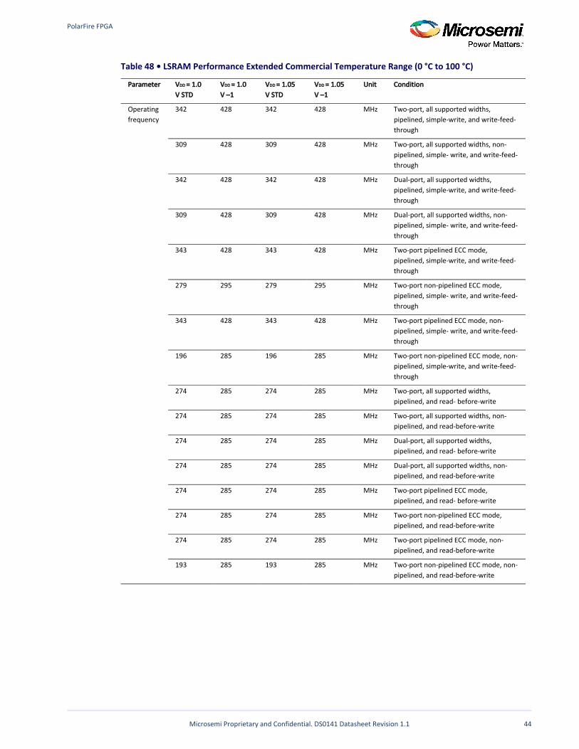
PolarFire FPGA
Microsemi Proprietary and Confidential. DS0141 Datasheet Revision 1.1 44
Table 48 • LSRAM Performance Extended Commercial Temperature Range (0 °C to 100 °C)
Parameter VDD = 1.0 STDV
VDD = 1.0 –1V
VDD = 1.05 STDV
VDD = 1.05 –1V
Unit Condition
Operating frequency
342 428 342 428 MHz Two-port, all supported widths, pipelined, simple-write, and write-feed-through
309 428 309 428 MHz Two-port, all supported widths, non-pipelined, simple- write, and write-feed-through
342 428 342 428 MHz Dual-port, all supported widths, pipelined, simple-write, and write-feed-through
309 428 309 428 MHz Dual-port, all supported widths, non-pipelined, simple- write, and write-feed-through
343 428 343 428 MHz Two-port pipelined ECC mode, pipelined, simple-write, and write-feed-through
279 295 279 295 MHz Two-port non-pipelined ECC mode, pipelined, simple- write, and write-feed-through
343 428 343 428 MHz Two-port pipelined ECC mode, non-pipelined, simple- write, and write-feed-through
196 285 196 285 MHz Two-port non-pipelined ECC mode, non-pipelined, simple-write, and write-feed-through
274 285 274 285 MHz Two-port, all supported widths, pipelined, and read- before-write
274 285 274 285 MHz Two-port, all supported widths, non-pipelined, and read-before-write
274 285 274 285 MHz Dual-port, all supported widths, pipelined, and read- before-write
274 285 274 285 MHz Dual-port, all supported widths, non-pipelined, and read-before-write
274 285 274 285 MHz Two-port pipelined ECC mode, pipelined, and read- before-write
274 285 274 285 MHz Two-port non-pipelined ECC mode, pipelined, and read-before-write
274 285 274 285 MHz Two-port pipelined ECC mode, non-pipelined, and read-before-write
193 285 193 285 MHz Two-port non-pipelined ECC mode, non-pipelined, and read-before-write
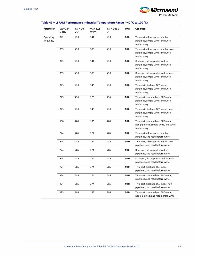
PolarFire FPGA
Microsemi Proprietary and Confidential. DS0141 Datasheet Revision 1.1 45
Table 49 • LSRAM Performance Industrial Temperature Range (–40 °C to 100 °C)
Parameter VDD = 1.0 STDV
VDD = 1.0 –1V
VDD = 1.05 STDV
VDD = 1.05 V–1
Unit Condition
Operating frequency
342 428 342 428 MHz Two-port, all supported widths, pipelined, simple-write, and write-feed-through
309 428 309 428 MHz Two-port, all supported widths, non-pipelined, simple-write, and write-feed-through
342 428 342 428 MHz Dual-port, all supported widths, pipelined, simple-write, and write-feed-through
309 428 309 428 MHz Dual-port, all supported widths, non-pipelined, simple-write, and write-feed-through
343 428 343 428 MHz Two-port pipelined ECC mode, pipelined, simple-write, and write-feed-through
279 295 279 295 MHz Two-port non-pipelined ECC mode, pipelined, simple-write, and write-feed-through
343 428 343 428 MHz Two-port pipelined ECC mode, non-pipelined, simple-write, and write-feed-through
196 285 196 285 MHz Two-port non-pipelined ECC mode, non-pipelined, simple-write, and write-feed-through
274 285 274 285 MHz Two-port, all supported widths, pipelined, and read-before-write
274 285 274 285 MHz Two-port, all supported widths, non-pipelined, and read-before-write
274 285 274 285 MHz Dual-port, all supported widths, pipelined, and read-before-write
274 285 274 285 MHz Dual-port, all supported widths, non-pipelined, and read-before-write
274 285 274 285 MHz Two-port pipelined ECC mode, pipelined, and read-before-write
274 285 274 285 MHz Two-port non-pipelined ECC mode, pipelined, and read-before-write
274 285 274 285 MHz Two-port pipelined ECC mode, non-pipelined, and read-before-write
193 285 193 285 MHz Two-port non-pipelined ECC mode, non-pipelined, and read-before-write
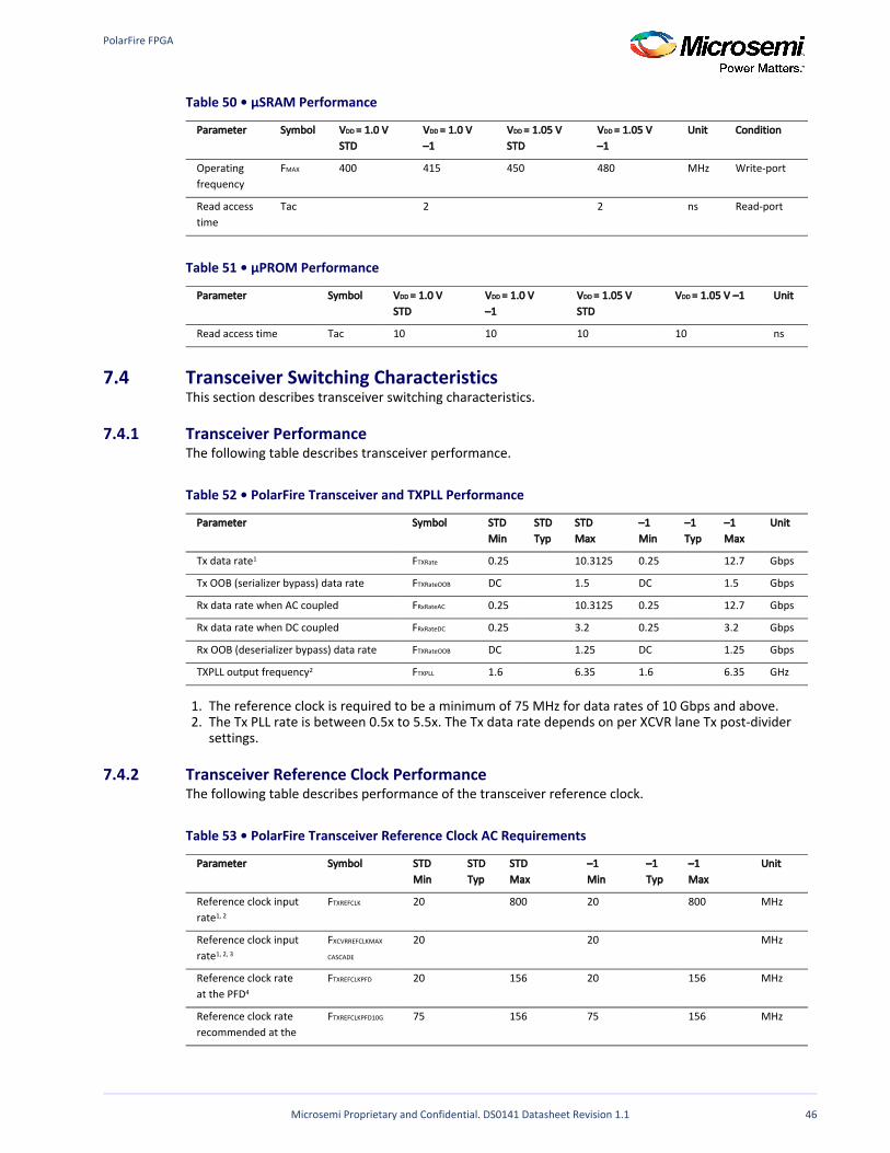
PolarFire FPGA
Microsemi Proprietary and Confidential. DS0141 Datasheet Revision 1.1 46
1. 2.
Table 50 • µSRAM Performance
Parameter Symbol VDD = 1.0 VSTD
VDD = 1.0 V–1
VDD = 1.05 VSTD
VDD = 1.05 V–1
Unit Condition
Operating frequency
FMAX 400 415 450 480 MHz Write-port
Read access time
Tac 2 2 ns Read-port
Table 51 • µPROM Performance
Parameter Symbol VDD = 1.0 VSTD
VDD = 1.0 V–1
VDD = 1.05 VSTD
–1VDD = 1.05 V Unit
Read access time Tac 10 10 10 10 ns
7.4 Transceiver Switching CharacteristicsThis section describes transceiver switching characteristics.
7.4.1 Transceiver PerformanceThe following table describes transceiver performance.
Table 52 • PolarFire Transceiver and TXPLL Performance
Parameter Symbol STDMin
STDTyp
STDMax
–1Min
–1Typ
–1Max
Unit
Tx data rate1 FTXRate 0.25 10.3125 0.25 12.7 Gbps
Tx OOB (serializer bypass) data rate FTXRateOOB DC 1.5 DC 1.5 Gbps
Rx data rate when AC coupled FRxRateAC 0.25 10.3125 0.25 12.7 Gbps
Rx data rate when DC coupled FRxRateDC 0.25 3.2 0.25 3.2 Gbps
Rx OOB (deserializer bypass) data rate FTXRateOOB DC 1.25 DC 1.25 Gbps
TXPLL output frequency2 FTXPLL 1.6 6.35 1.6 6.35 GHz
The reference clock is required to be a minimum of 75 MHz for data rates of 10 Gbps and above.The Tx PLL rate is between 0.5x to 5.5x. The Tx data rate depends on per XCVR lane Tx post-divider settings.
7.4.2 Transceiver Reference Clock PerformanceThe following table describes performance of the transceiver reference clock.
Table 53 • PolarFire Transceiver Reference Clock AC Requirements
Parameter Symbol STDMin
STDTyp
STDMax
–1Min
–1Typ
–1Max
Unit
Reference clock input rate1, 2
FTXREFCLK 20 800 20 800 MHz
Reference clock input rate1, 2, 3
FXCVRREFCLKMAX
CASCADE
20 20 MHz
Reference clock rate at the PFD4
FTXREFCLKPFD 20 156 20 156 MHz
Reference clock rate recommended at the
FTXREFCLKPFD10G 75 156 75 156 MHz
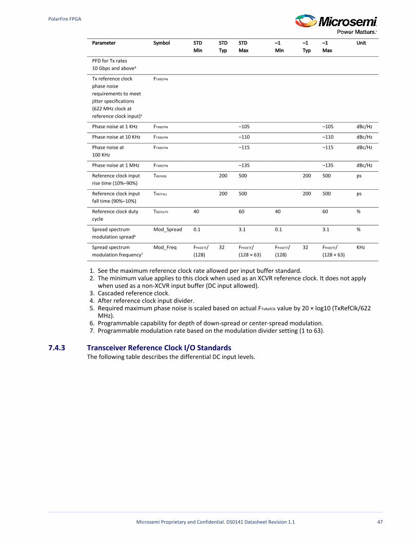
PolarFire FPGA
Microsemi Proprietary and Confidential. DS0141 Datasheet Revision 1.1 47
1. 2.
3. 4. 5.
6. 7.
Parameter Symbol STDMin
STDTyp
STDMax
–1Min
–1Typ
–1Max
Unit
PFD for Tx rates10 Gbps and above4
Tx reference clock phase noise requirements to meet jitter specifications (622 MHz clock at reference clock input)5
FTXREFPN
Phase noise at 1 KHz FTXREFPN –105 –105 dBc/Hz
Phase noise at 10 KHz FTXREFPN –110 –110 dBc/Hz
Phase noise at100 KHz
FTXREFPN –115 –115 dBc/Hz
Phase noise at 1 MHz FTXREFPN –135 –135 dBc/Hz
Reference clock input rise time (10%–90%)
TREFRISE 200 500 200 500 ps
Reference clock input fall time (90%–10%)
TREFFALL 200 500 200 500 ps
Reference clock duty cycle
TREFDUTY 40 60 40 60 %
Spread spectrum modulation spread6
Mod_Spread 0.1 3.1 0.1 3.1 %
Spread spectrum modulation frequency7
Mod_Freq F /PHDETF
(128)32 F /PHDETF
(128 × 63)F /PHDETF
(128)32 F /PHDETF
(128 × 63)KHz
See the maximum reference clock rate allowed per input buffer standard.The minimum value applies to this clock when used as an XCVR reference clock. It does not apply when used as a non-XCVR input buffer (DC input allowed).Cascaded reference clock.After reference clock input divider.Required maximum phase noise is scaled based on actual F value by 20 × log10 (TxRefClk/622 TxRefClk
MHz).Programmable capability for depth of down-spread or center-spread modulation.Programmable modulation rate based on the modulation divider setting (1 to 63).
7.4.3 Transceiver Reference Clock I/O StandardsThe following table describes the differential DC input levels.
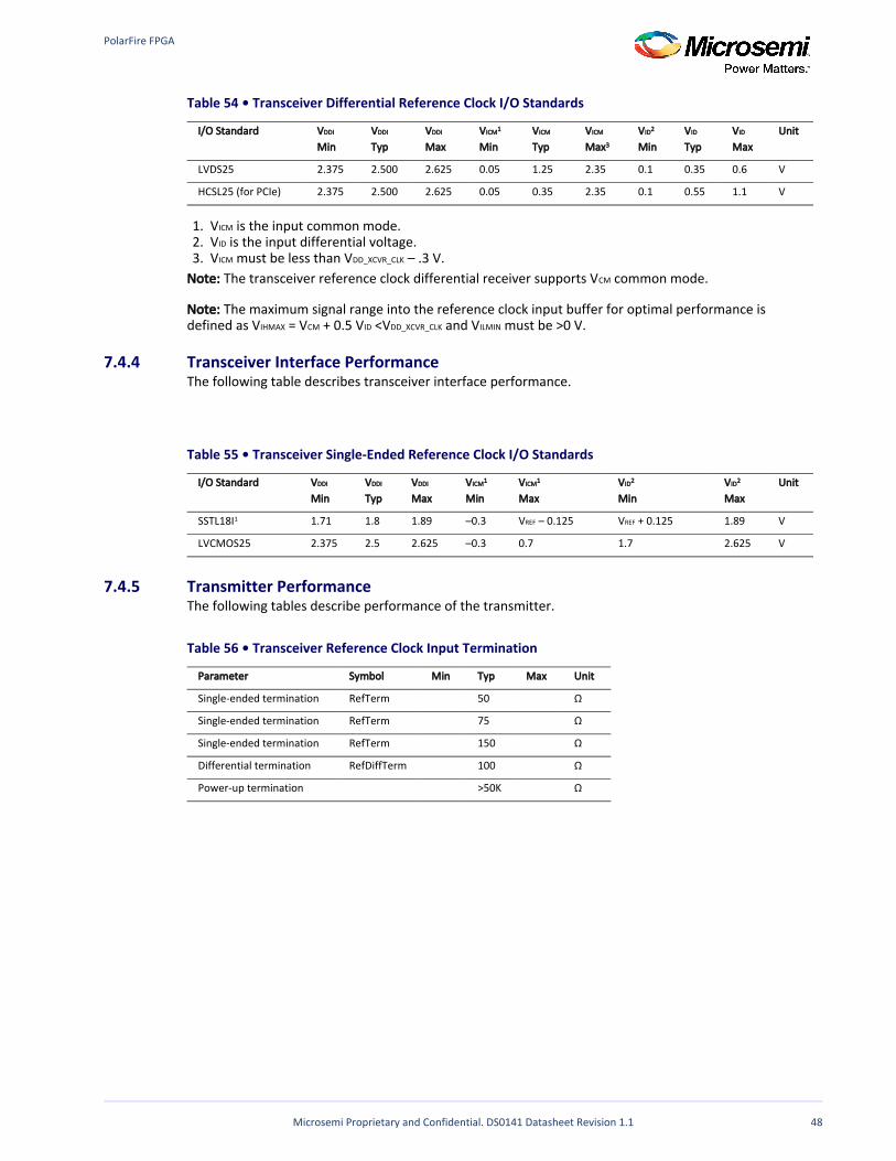
PolarFire FPGA
Microsemi Proprietary and Confidential. DS0141 Datasheet Revision 1.1 48
1. 2. 3.
Table 54 • Transceiver Differential Reference Clock I/O Standards
I/O Standard VDDI
Min VDDI
Typ VDDI
Max VICM1
Min VICM
Typ VICM
Max3
V ID2
MinV ID
TypV ID
MaxUnit
LVDS25 2.375 2.500 2.625 0.05 1.25 2.35 0.1 0.35 0.6 V
HCSL25 (for PCIe) 2.375 2.500 2.625 0.05 0.35 2.35 0.1 0.55 1.1 V
V is the input common mode.ICM
V is the input differential voltage.ID
V must be less than V – .3 V.ICM DD_XCVR_CLK
Note: The transceiver reference clock differential receiver supports V common mode.CM
Note: The maximum signal range into the reference clock input buffer for optimal performance is defined as V = V + 0.5 V <V and V must be >0 V.IHMAX CM ID DD_XCVR_CLK ILMIN
7.4.4 Transceiver Interface PerformanceThe following table describes transceiver interface performance.
Table 55 • Transceiver Single-Ended Reference Clock I/O Standards
I/O Standard VDDI
Min VDDI
Typ VDDI
Max VICM1
Min VICM1
Max VID2
Min VID2
MaxUnit
SSTL18I1 1.71 1.8 1.89 –0.3 V – 0.125REF V + 0.125REF 1.89 V
LVCMOS25 2.375 2.5 2.625 –0.3 0.7 1.7 2.625 V
7.4.5 Transmitter PerformanceThe following tables describe performance of the transmitter.
Table 56 • Transceiver Reference Clock Input Termination
Parameter Symbol Min Typ Max Unit
Single-ended termination RefTerm 50 Ω
Single-ended termination RefTerm 75 Ω
Single-ended termination RefTerm 150 Ω
Differential termination RefDiffTerm 100 Ω
Power-up termination >50K Ω
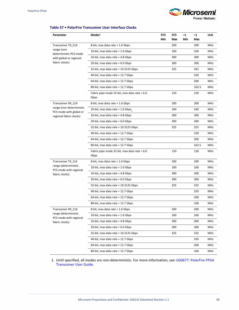
PolarFire FPGA
Microsemi Proprietary and Confidential. DS0141 Datasheet Revision 1.1 49
1.
Table 57 • PolarFire Transceiver User Interface Clocks
Parameter Modes1 STDMin
STDMax
–1Min
–1Max
Unit
Transceiver TX_CLK range (non-deterministic PCS mode with global or regional fabric clocks)
8-bit, max data rate = 1.6 Gbps 200 200 MHz
10-bit, max data rate = 1.6 Gbps 160 160 MHz
16-bit, max data rate = 4.8 Gbps 300 300 MHz
20-bit, max data rate = 6.0 Gbps 300 300 MHz
32-bit, max data rate = 10.3125 Gbps 325 325 MHz
40-bit, max data rate = 12.7 Gbps 320 MHz
64-bit, max data rate = 12.7 Gbps 200 MHz
80-bit, max data rate = 12.7 Gbps 162.5 MHz
Fabric pipe mode 32-bit, max data rate = 6.0 Gbps
150 150 MHz
Transceiver RX_CLK range (non-deterministicPCS mode with global or regional fabric clocks)
8-bit, max data rate = 1.6 Gbps 200 200 MHz
10-bit, max data rate = 1.6 Gbps 160 160 MHz
16-bit, max data rate = 4.8 Gbps 300 300 MHz
20-bit, max data rate = 6.0 Gbps 300 300 MHz
32-bit, max data rate = 10.3125 Gbps 325 325 MHz
40-bit, max data rate = 12.7 Gbps 320 MHz
64-bit, max data rate = 12.7 Gbps 200 MHz
80-bit, max data rate = 12.7 Gbps 162.5 MHz
Fabric pipe mode 32-bit, max data rate = 6.0 Gbps
150 150 MHz
Transceiver TX_CLK range (deterministicPCS mode with regional fabric clocks)
8-bit, max data rate = 1.6 Gbps 200 200 MHz
10-bit, max data rate = 1.6 Gbps 160 160 MHz
16-bit, max data rate = 4.8 Gbps 300 300 MHz
20-bit, max data rate = 6.0 Gbps 300 300 MHz
32-bit, max data rate = 10.3125 Gbps 325 325 MHz
40-bit, max data rate = 12.7 Gbps 320 MHz
64-bit, max data rate = 12.7 Gbps 200 MHz
80-bit, max data rate = 12.7 Gbps 160 MHz
Transceiver RX_CLK range (deterministicPCS mode with regional fabric clocks)
8-bit, max data rate = 1.6 Gbps 200 200 MHz
10-bit, max data rate = 1.6 Gbps 160 160 MHz
16-bit, max data rate = 4.8 Gbps 300 300 MHz
20-bit, max data rate = 6.0 Gbps 300 300 MHz
32-bit, max data rate = 10.3125 Gbps 325 325 MHz
40-bit, max data rate = 12.7 Gbps 320 MHz
64-bit, max data rate = 12.7 Gbps 200 MHz
80-bit, max data rate = 12.7 Gbps 160 MHz
Until specified, all modes are non-deterministic. For more information, see UG0677: PolarFire FPGA .Transceiver User Guide
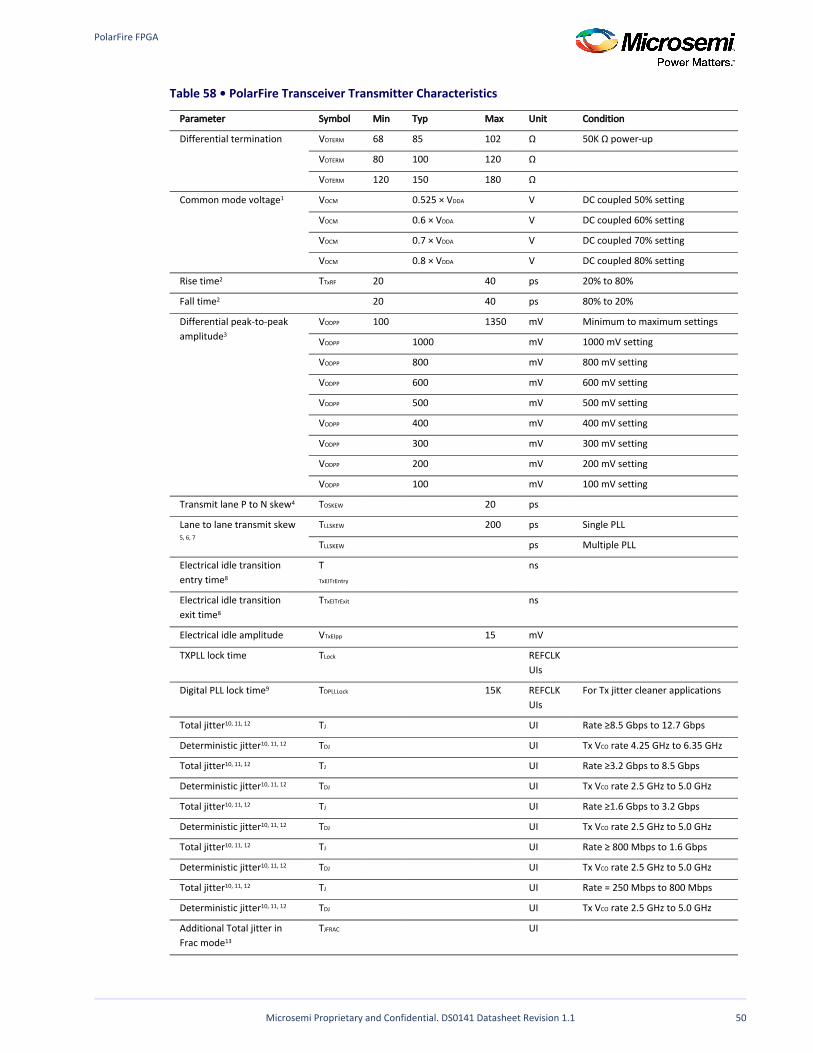
PolarFire FPGA
Microsemi Proprietary and Confidential. DS0141 Datasheet Revision 1.1 50
Table 58 • PolarFire Transceiver Transmitter Characteristics
Parameter Symbol Min Typ Max Unit Condition
Differential termination VOTERM 68 85 102 Ω 50K Ω power-up
VOTERM 80 100 120 Ω
VOTERM 120 150 180 Ω
Common mode voltage1 VOCM 0.525 × VDDA V DC coupled 50% setting
VOCM 0.6 × VDDA V DC coupled 60% setting
VOCM 0.7 × VDDA V DC coupled 70% setting
VOCM 0.8 × VDDA V DC coupled 80% setting
Rise time2 TTxRF 20 40 ps 20% to 80%
Fall time2 20 40 ps 80% to 20%
Differential peak-to-peak amplitude3
VODPP 100 1350 mV Minimum to maximum settings
VODPP 1000 mV 1000 mV setting
VODPP 800 mV 800 mV setting
VODPP 600 mV 600 mV setting
VODPP 500 mV 500 mV setting
VODPP 400 mV 400 mV setting
VODPP 300 mV 300 mV setting
VODPP 200 mV 200 mV setting
VODPP 100 mV 100 mV setting
Transmit lane P to N skew4 TOSKEW 20 ps
Lane to lane transmit skew5, 6, 7
TLLSKEW 200 ps Single PLL
TLLSKEW ps Multiple PLL
Electrical idle transition entry time8
TTxEITrEntry
ns
Electrical idle transition exit time8
TTxEITrExit ns
Electrical idle amplitude VTxEIpp 15 mV
TXPLL lock time TLock REFCLKUIs
Digital PLL lock time9 TDPLLLock 15K REFCLK UIs
For Tx jitter cleaner applications
Total jitter10, 11, 12 TJ UI Rate ≥8.5 Gbps to 12.7 Gbps
Deterministic jitter10, 11, 12 TDJ UI Tx V rate 4.25 GHz to 6.35 GHzCO
Total jitter10, 11, 12 TJ UI Rate ≥3.2 Gbps to 8.5 Gbps
Deterministic jitter10, 11, 12 TDJ UI Tx V rate 2.5 GHz to 5.0 GHzCO
Total jitter10, 11, 12 TJ UI Rate ≥1.6 Gbps to 3.2 Gbps
Deterministic jitter10, 11, 12 TDJ UI Tx V rate 2.5 GHz to 5.0 GHzCO
Total jitter10, 11, 12 TJ UI Rate ≥ 800 Mbps to 1.6 Gbps
Deterministic jitter10, 11, 12 TDJ UI Tx V rate 2.5 GHz to 5.0 GHzCO
Total jitter10, 11, 12 TJ UI Rate = 250 Mbps to 800 Mbps
Deterministic jitter10, 11, 12 TDJ UI Tx V rate 2.5 GHz to 5.0 GHzCO
Additional Total jitter in Frac mode13
TJFRAC UI
PolarFire FPGA
Microsemi Proprietary and Confidential. DS0141 Datasheet Revision 1.1 51
1. 2. 3. 4. 5. 6. 7.
8. 9.
10.
11.
12.
13.
Parameter Symbol Min Typ Max Unit Condition
Additional deterministic jitter in Frac mode13
TDJFRAC UI
Increased DC common mode settings above 50% reduce allowed V output swing capabilities.OD
Adjustable through transmit emphasis.V = 1.0 V ±30 mV.DDA
With estimated package differences.Single PLL applies to all four lanes in the same quad location with the same TxPLL.Multiple PLL applies to N lanes using multiple TxPLLs from different quad locations.For more information about how to transmit align multiple lanes from different quad locations, see
.UG0677: PolarFire FPGA Transceiver User GuideFrom the PMA mode, the TX_ELEC_IDLE port to the XCVR TXP/N pins.FTxRefClk = 75 MHz with typical settings.Jitter measurements are obtained using the TXPL_SSC and/or TXPLL in integer mode with the slowest possible V rate with a reference clock of at least 100 MHz that meets the input phase CO
noise specifications.Improved jitter characteristics for a specific industry standard are possible in many cases due to improved reference clock or higher V rate used.CO
Tx jitter is specified with all transmitters on the device enabled, a 10-12 bit error rate (BER) and Tx data pattern of PRBS2 .7
Additional T when Fractional-N mode is enabled.J
7.4.6 Receiver PerformanceThe following table describes performance of the receiver.
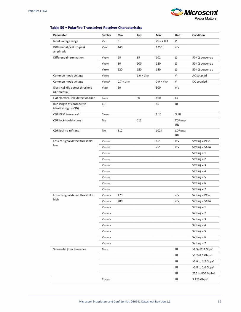
PolarFire FPGA
Microsemi Proprietary and Confidential. DS0141 Datasheet Revision 1.1 52
Table 59 • PolarFire Transceiver Receiver Characteristics
Parameter Symbol Min Typ Max Unit Condition
Input voltage range VIN 0 V + 0.3DDA V
Differential peak-to-peak amplitude
VIDPP 140 1250 mV
Differential termination VITERM 68 85 102 Ω 50K Ω power-up
VITERM 80 100 120 Ω 50K Ω power-up
VITERM 120 150 180 Ω 50K Ω power-up
Common mode voltage VICMAC 1.0 × VDDA V AC coupled
Common mode voltage VICMDC1 0.7 × VDDA 0.9 × VDDA V DC coupled
Electrical idle detect threshold (differential)
VEIDET 60 300 mV
Exit electrical idle detection time TEIDET 50 100 ns
Run length of consecutive identical digits (CID)
CID 85 UI
CDR PPM tolerance2 CDRPPM 1.15 % UI
CDR lock-to-data time TLTD 512 CDRREFCLK
UIs
CDR lock-to-ref time TLTF 512 1024 CDRREFCLK
UIs
Loss-of-signal detect threshold-low
VDETLOW 653 mV Setting = PCIe
VDETLOW 754 mV Setting = SATA
VDETLOW Setting = 1
VDETLOW Setting = 2
VDETLOW Setting = 3
VDETLOW Setting = 4
VDETLOW Setting = 5
VDETLOW Setting = 6
VDETLOW Setting = 7
Loss-of-signal detect threshold-high
VDETHIGH 1754 mV Setting = PCIe
VDETHIGH 2004 mV Setting = SATA
VDETHIGH Setting = 1
VDETHIGH Setting = 2
VDETHIGH Setting = 3
VDETHIGH Setting = 4
VDETHIGH Setting = 5
VDETHIGH Setting = 6
VDETHIGH Setting = 7
Sinusoidal jitter tolerance TSJTOL UI >8.5–12.7 Gbps4
UI >3.2–8.5 Gbps5
UI >1.6 to 3.2 Gbps5
UI >0.8 to 1.6 Gbps6
UI 250 to 800 Mpbs6
TTJTOLSE UI 3.125 Gbps5
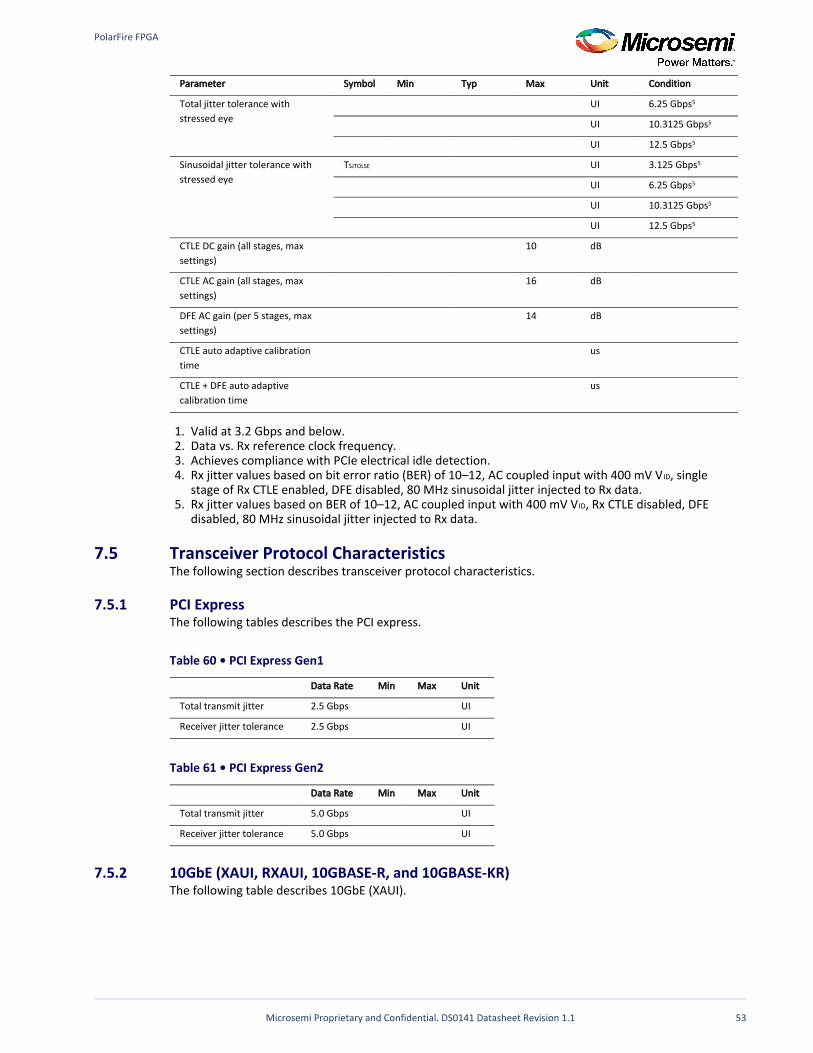
PolarFire FPGA
Microsemi Proprietary and Confidential. DS0141 Datasheet Revision 1.1 53
1. 2. 3. 4.
5.
Parameter Symbol Min Typ Max Unit Condition
Total jitter tolerance with stressed eye
UI 6.25 Gbps5
UI 10.3125 Gbps5
UI 12.5 Gbps5
Sinusoidal jitter tolerance with stressed eye
TSJTOLSE UI 3.125 Gbps5
UI 6.25 Gbps5
UI 10.3125 Gbps5
UI 12.5 Gbps5
CTLE DC gain (all stages, max settings)
10 dB
CTLE AC gain (all stages, max settings)
16 dB
DFE AC gain (per 5 stages, max settings)
14 dB
CTLE auto adaptive calibration time
us
CTLE + DFE auto adaptive calibration time
us
Valid at 3.2 Gbps and below.Data vs. Rx reference clock frequency.Achieves compliance with PCIe electrical idle detection.Rx jitter values based on bit error ratio (BER) of 10–12, AC coupled input with 400 mV V , single ID
stage of Rx CTLE enabled, DFE disabled, 80 MHz sinusoidal jitter injected to Rx data.Rx jitter values based on BER of 10–12, AC coupled input with 400 mV V , Rx CTLE disabled, DFE ID
disabled, 80 MHz sinusoidal jitter injected to Rx data.
7.5 Transceiver Protocol CharacteristicsThe following section describes transceiver protocol characteristics.
7.5.1 PCI ExpressThe following tables describes the PCI express.
Table 60 • PCI Express Gen1
Data Rate Min Max Unit
Total transmit jitter 2.5 Gbps UI
Receiver jitter tolerance 2.5 Gbps UI
Table 61 • PCI Express Gen2
Data Rate Min Max Unit
Total transmit jitter 5.0 Gbps UI
Receiver jitter tolerance 5.0 Gbps UI
7.5.2 10GbE (XAUI, RXAUI, 10GBASE-R, and 10GBASE-KR)The following table describes 10GbE (XAUI).
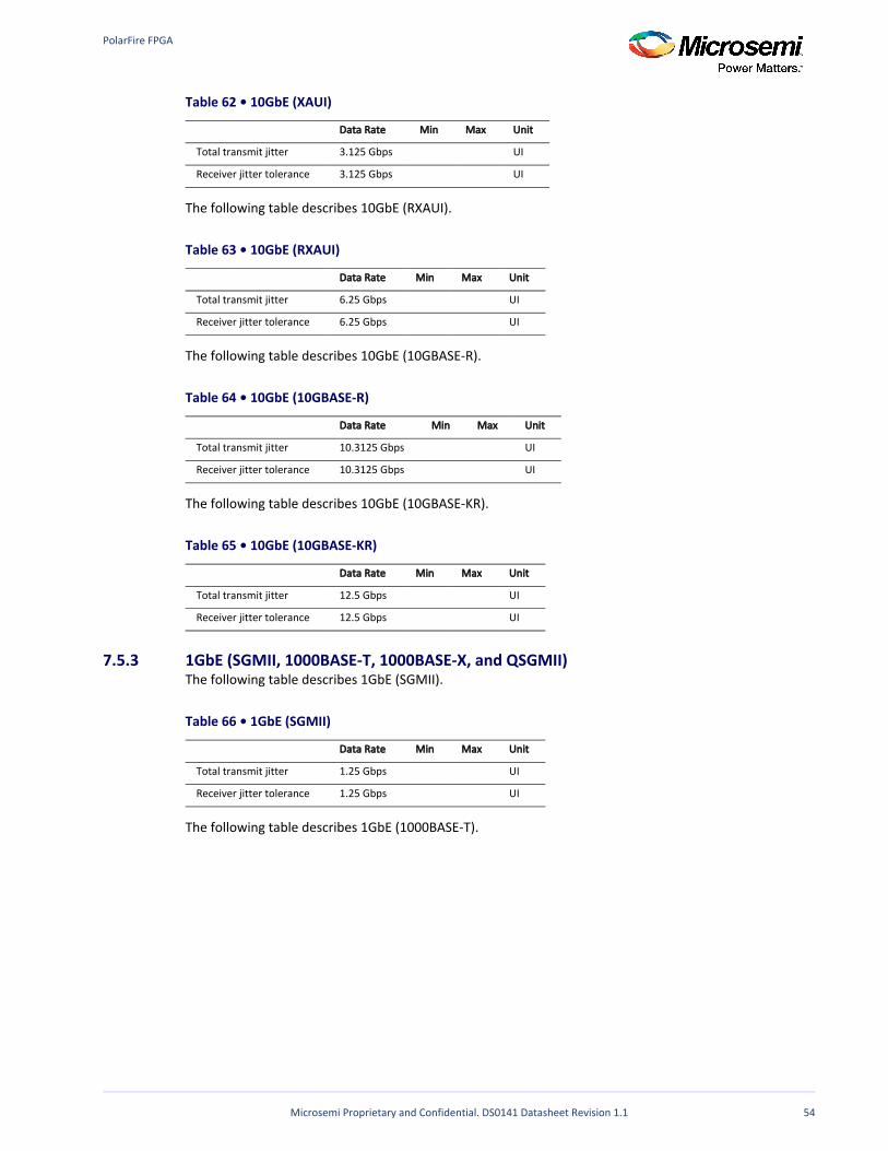
PolarFire FPGA
Microsemi Proprietary and Confidential. DS0141 Datasheet Revision 1.1 54
Table 62 • 10GbE (XAUI)
Data Rate Min Max Unit
Total transmit jitter 3.125 Gbps UI
Receiver jitter tolerance 3.125 Gbps UI
The following table describes 10GbE (RXAUI).
Table 63 • 10GbE (RXAUI)
Data Rate Min Max Unit
Total transmit jitter 6.25 Gbps UI
Receiver jitter tolerance 6.25 Gbps UI
The following table describes 10GbE (10GBASE-R).
Table 64 • 10GbE (10GBASE-R)
Data Rate Min Max Unit
Total transmit jitter 10.3125 Gbps UI
Receiver jitter tolerance 10.3125 Gbps UI
The following table describes 10GbE (10GBASE-KR).
Table 65 • 10GbE (10GBASE-KR)
Data Rate Min Max Unit
Total transmit jitter 12.5 Gbps UI
Receiver jitter tolerance 12.5 Gbps UI
7.5.3 1GbE (SGMII, 1000BASE-T, 1000BASE-X, and QSGMII)The following table describes 1GbE (SGMII).
Table 66 • 1GbE (SGMII)
Data Rate Min Max Unit
Total transmit jitter 1.25 Gbps UI
Receiver jitter tolerance 1.25 Gbps UI
The following table describes 1GbE (1000BASE-T).
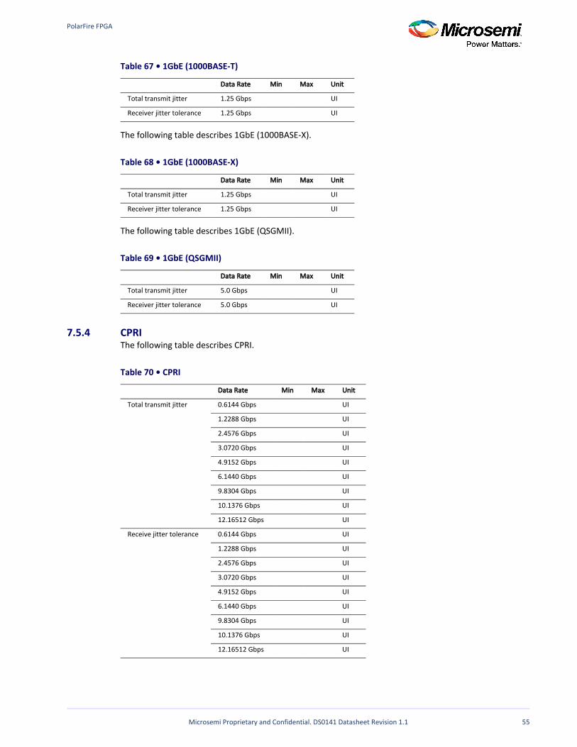
PolarFire FPGA
Microsemi Proprietary and Confidential. DS0141 Datasheet Revision 1.1 55
Table 67 • 1GbE (1000BASE-T)
Data Rate Min Max Unit
Total transmit jitter 1.25 Gbps UI
Receiver jitter tolerance 1.25 Gbps UI
The following table describes 1GbE (1000BASE-X).
Table 68 • 1GbE (1000BASE-X)
Data Rate Min Max Unit
Total transmit jitter 1.25 Gbps UI
Receiver jitter tolerance 1.25 Gbps UI
The following table describes 1GbE (QSGMII).
Table 69 • 1GbE (QSGMII)
Data Rate Min Max Unit
Total transmit jitter 5.0 Gbps UI
Receiver jitter tolerance 5.0 Gbps UI
7.5.4 CPRIThe following table describes CPRI.
Table 70 • CPRI
Data Rate Min Max Unit
Total transmit jitter 0.6144 Gbps UI
1.2288 Gbps UI
2.4576 Gbps UI
3.0720 Gbps UI
4.9152 Gbps UI
6.1440 Gbps UI
9.8304 Gbps UI
10.1376 Gbps UI
12.16512 Gbps UI
Receive jitter tolerance 0.6144 Gbps UI
1.2288 Gbps UI
2.4576 Gbps UI
3.0720 Gbps UI
4.9152 Gbps UI
6.1440 Gbps UI
9.8304 Gbps UI
10.1376 Gbps UI
12.16512 Gbps UI
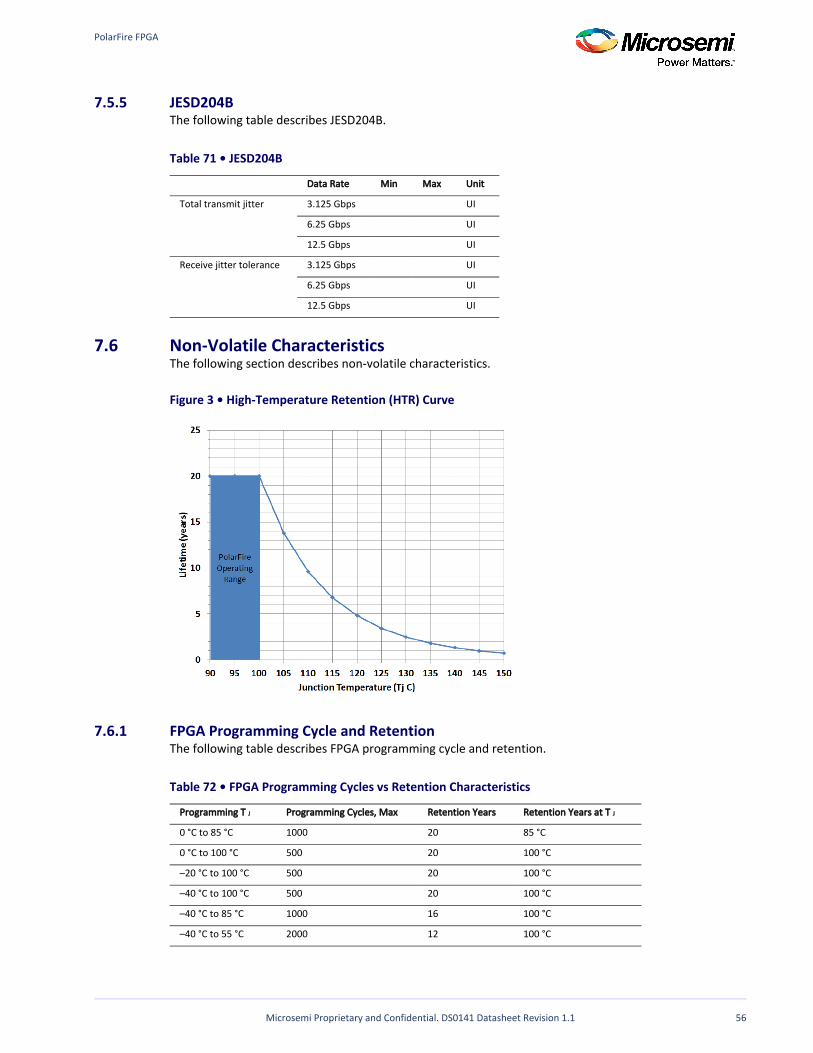
PolarFire FPGA
Microsemi Proprietary and Confidential. DS0141 Datasheet Revision 1.1 56
7.5.5 JESD204BThe following table describes JESD204B.
Table 71 • JESD204B
Data Rate Min Max Unit
Total transmit jitter 3.125 Gbps UI
6.25 Gbps UI
12.5 Gbps UI
Receive jitter tolerance 3.125 Gbps UI
6.25 Gbps UI
12.5 Gbps UI
7.6 Non-Volatile CharacteristicsThe following section describes non-volatile characteristics.
Figure 3 • High-Temperature Retention (HTR) Curve
7.6.1 FPGA Programming Cycle and RetentionThe following table describes FPGA programming cycle and retention.
Table 72 • FPGA Programming Cycles vs Retention Characteristics
Programming T J Programming Cycles, Max Retention Years Retention Years at T J
0 °C to 85 °C 1000 20 85 °C
0 °C to 100 °C 500 20 100 °C
–20 °C to 100 °C 500 20 100 °C
–40 °C to 100 °C 500 20 100 °C
–40 °C to 85 °C 1000 16 100 °C
–40 °C to 55 °C 2000 12 100 °C
Note: Power supplied to the device must be valid during programming operations such as programming,
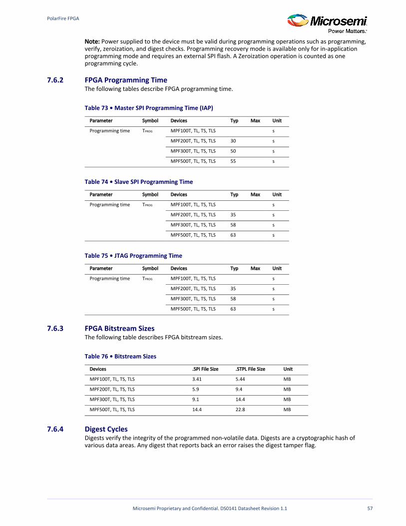
PolarFire FPGA
Microsemi Proprietary and Confidential. DS0141 Datasheet Revision 1.1 57
Note: Power supplied to the device must be valid during programming operations such as programming,verify, zeroization, and digest checks. Programming recovery mode is available only for in-applicationprogramming mode and requires an external SPI flash. A Zeroization operation is counted as one programming cycle.
7.6.2 FPGA Programming TimeThe following tables describe FPGA programming time.
Table 73 • Master SPI Programming Time (IAP)
Parameter Symbol Devices Typ Max Unit
Programming time TPROG MPF100T, TL, TS, TLS s
MPF200T, TL, TS, TLS 30 s
MPF300T, TL, TS, TLS 50 s
MPF500T, TL, TS, TLS 55 s
Table 74 • Slave SPI Programming Time
Parameter Symbol Devices Typ Max Unit
Programming time TPROG MPF100T, TL, TS, TLS s
MPF200T, TL, TS, TLS 35 s
MPF300T, TL, TS, TLS 58 s
MPF500T, TL, TS, TLS 63 s
Table 75 • JTAG Programming Time
Parameter Symbol Devices Typ Max Unit
Programming time TPROG MPF100T, TL, TS, TLS s
MPF200T, TL, TS, TLS 35 s
MPF300T, TL, TS, TLS 58 s
MPF500T, TL, TS, TLS 63 s
7.6.3 FPGA Bitstream SizesThe following table describes FPGA bitstream sizes.
Table 76 • Bitstream Sizes
Devices .SPI File Size .STPL File Size Unit
MPF100T, TL, TS, TLS 3.41 5.44 MB
MPF200T, TL, TS, TLS 5.9 9.4 MB
MPF300T, TL, TS, TLS 9.1 14.4 MB
MPF500T, TL, TS, TLS 14.4 22.8 MB
7.6.4 Digest CyclesDigests verify the integrity of the programmed non-volatile data. Digests are a cryptographic hash of various data areas. Any digest that reports back an error raises the digest tamper flag.
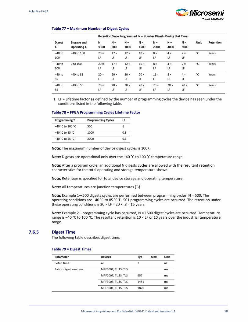
PolarFire FPGA
Microsemi Proprietary and Confidential. DS0141 Datasheet Revision 1.1 58
1.
Table 77 • Maximum Number of Digest Cycles
Retention Since Programmed. N = Number Digests During that Time1
Digest TJ
Storage and Operating TJ
N ≤300
N = 500
N = 1000
N = 1500
N = 2000
N = 4000
N = 6000
Unit Retention
–40 to 100
–40 to 100 20 × LF
17 × LF
12 × LF
10 × LF
8 × LF
4 × LF
2 × LF
°C Years
–40 to 100
0 to 100 20 × LF
17 × LF
12 × LF
10 × LF
8 × LF
4 × LF
2 × LF
°C Years
–40 to 85
–40 to 85 20 × LF
20 × LF
20 × LF
20 × LF
16 × LF
8 × LF
4 × LF
°C Years
–40 to 55
–40 to 55 20 × LF
20 × LF
20 × LF
20 × LF
20 × LF
20 × LF
20 × LF
°C Years
LF = Lifetime factor as defined by the number of programming cycles the device has seen under the conditions listed in the following table.
Table 78 • FPGA Programming Cycles Lifetime Factor
Programming T J Programming Cycles LF
–40 °C to 100 °C 500 1
–40 °C to 85 °C 1000 0.8
–40 °C to 55 °C 2000 0.6
Note: The maximum number of device digest cycles is 100K.
Note: Digests are operational only over the –40 °C to 100 °C temperature range.
Note: After a program cycle, an additional N digests cycles are allowed with the resultant retention characteristics for the total operating and storage temperature shown.
Note: Retention is specified for total device storage and operating temperature.
Note: All temperatures are junction temperatures (T ).J
Note: Example 1—500 digests cycles are performed between programming cycles. N = 500. The operating conditions are –40 °C to 85 °C T . 501 programming cycles are occurred. The retention under J
these operating conditions is 20 × LF = 20 × .8 = 16 years.
Note: Example 2—programming cycle has occurred, N = 1500 digest cycles are occurred. Temperature range is –40 °C to 100 °C. The resultant retention is 10 × LF or 10 years over the industrial temperature range.
7.6.5 Digest TimeThe following table describes digest time.
Table 79 • Digest Times
Parameter Devices Typ Max Unit
Setup time All 2 us
Fabric digest run time MPF100T, TL,TS, TLS ms
MPF200T, TL,TS, TLS 957 ms
MPF300T, TL,TS, TLS 1451 ms
MPF500T, TL,TS, TLS 1876 ms
PolarFire FPGA
Microsemi Proprietary and Confidential. DS0141 Datasheet Revision 1.1 59
1. 2.
Parameter Devices Typ Max Unit
UFS CC digest run time MPF100T, TL, TS, TLS us
MPF200T, TL, TS, TLS 28 us
MPF300T, TL, TS, TLS 28 us
MPF500T, TL, TS, TLS 28 us
sNVM digest run time1 MPF100T, TL, TS, TLS ms
MPF200T, TL, TS, TLS ms
MPF300T, TL, TS, TLS ms
MPF500T, TL, TS, TLS ms
UFS UL digest run time MPF100T, TL, TS, TLS us
MPF200T, TL, TS, TLS 41 us
MPF300T, TL, TS, TLS 41 us
MPF500T, TL, TS, TLS 41 us
User key digest run time2 MPF100T, TL, TS, TLS us
MPF200T, TL, TS, TLS 564 us
MPF300T, TL, TS, TLS 564 us
MPF500T, TL, TS, TLS 564 us
UFS UPERM digest run time MPF100T, TL, TS, TLS us
MPF200T, TL, TS, TLS 28 us
MPF300T, TL, TS, TLS 28 us
MPF500T, TL, TS, TLS 28 us
Factory digest run time MPF100T, TL, TS, TLS us
MPF200T, TL, TS, TLS 461 us
MPF300T, TL, TS, TLS 461 us
MPF500T, TL, TS, TLS 461 us
The entire sNVM is used as ROM.Valid for User key 0 through 6.
Note: These times do not include the power-up to functional timing overhead when using digest checks on power-up.
7.6.6 Zeroization TimeThe following tables describe zeroization time. A zeroization operation is counted as one programming cycle.
Table 80 • Zeroization Times for MPF100T, TL, TS, and TLS Devices
Parameter Typ Max Unit Conditions
Time to enter zeroization ms Zip flag set
Time to destroy the fabric data1 ms Data erased
Time to destroy data in non-volatile memory (like new)1, 2 ms One iteration of scrubbing
Time to destroy data in non-volatile memory (recoverable)1, 3 ms One iteration of scrubbing
Time to destroy data in non-volatile memory (non-recoverable)1, 4 ms One iteration of scrubbing
Time to scrub the fabric data1 seconds Full scrubbing
PolarFire FPGA
Microsemi Proprietary and Confidential. DS0141 Datasheet Revision 1.1 60
1. 2. 3. 4.
5.
1. 2. 3. 4.
5.
Parameter Typ Max Unit Conditions
Time to scrub the pNVM data (like new)1, 2 seconds Full scrubbing
Time to scrub the pNVM data (recoverable)1, 3 seconds Full scrubbing
Time to scrub the fabric data pNVM data (non-recoverable)1, 4 seconds Full scrubbing
Time to verify5 seconds
Total completion time after entering zeroization.Like new mode—zeroizes user design security setting and sNVM content.Recoverable mode—zeroizes user design security setting, sNVM and factory keys.Non-recoverable mode—zeroizes user design security setting, sNVM and factory keys, and factory data required for programming.Time to verify after scrubbing completes.
Table 81 • Zeroization Times for MPF200T, TL, TS, and TLS Devices
Parameter Typ Max Unit Conditions
Time to enter zeroization ms Zip flag set
Time to destroy the fabric data1 ms Data erased
Time to destroy data in non-volatile memory (like new)1, 2 ms One iteration of scrubbing
Time to destroy data in non-volatile memory (recoverable)1, 3 ms One iteration of scrubbing
Time to destroy data in non-volatile memory (non-recoverable)1, 4 ms One iteration of scrubbing
Time to scrub the fabric data1 seconds Full scrubbing
Time to scrub the pNVM data (like new)1, 2 seconds Full scrubbing
Time to scrub the pNVM data (recoverable)1, 3 seconds Full scrubbing
Time to scrub the fabric data PNVM data (non-recoverable)1, 4 seconds Full scrubbing
Time to verify5 seconds
Total completion time after interning zeroization.Like new mode—zeroizes user design security setting and sNVM content.Recoverable mode—zeroizes user design security setting, sNVM and factory keys.Non-recoverable mode—zeroizes user design security setting, sNVM and factory keys, and factory data required for programming.Time to verify after scrubbing completes.
Table 82 • Zeroization Times for MPF300T, TL, TS, and TLS Devices
Parameter Typ Max Unit Conditions
Time to enter zeroization 8.7 ms Zip flag set
Time to destroy the Fabric data1 34.3 ms Data erased
Time to destroy data in non-volatile memory (like new)1, 2 801 ms One iteration of scrubbing
Time to destroy data in non-volatile memory (recoverable)1, 3 860 ms One iteration of scrubbing
Time to destroy data in non-volatile memory (non- recoverable)1, 4 909.9 ms One iteration of scrubbing
Time to scrub the fabric data1 1.151 seconds Full scrubbing
Time to scrub the pNVM data (like new)1, 2 2.4 seconds Full scrubbing
Time to scrub the pNVM data (recoverable)1, 3 2.58 seconds Full scrubbing
PolarFire FPGA
Microsemi Proprietary and Confidential. DS0141 Datasheet Revision 1.1 61
1. 2. 3. 4.
5.
1. 2. 3. 4.
5.
Parameter Typ Max Unit Conditions
Time to scrub the fabric data pNVM data (non-recoverable)1, 4 2.73 seconds Full scrubbing
Time to verify5 1.57 seconds
Total completion time after interning zeroization.Like new mode—zeroizes user design security setting and sNVM content.Recoverable mode—zeroizes user design security setting, sNVM and factory keys.Non-recoverable mode—zeroizes user design security setting, sNVM and factory keys, and factory data required for programming.Time to verify after scrubbing completes.
Table 83 • Zeroization Times for MPF500T, TL, TS, and TLS Devices
Parameter Typ Max Unit Conditions
Time to enter zeroization 8.7 ms Zip flag set
Time to destroy the fabric data1 34.3 ms Data erased
Time to destroy data in non-volatile memory (like new)1, 2 801 ms One iteration of scrubbing
Time to destroy data in non-volatile memory (recoverable)1, 3 860 ms One iteration of scrubbing
Time to destroy data in non-volatile memory (non-recoverable)1, 4 909.9 ms One iteration of scrubbing
Time to scrub the fabric data1 1.151 seconds Full scrubbing
Time to scrub the pNVM data (like new)1, 2 2.4 seconds Full scrubbing
Time to scrub the pNVM data (recoverable)1, 3 2.58 seconds Full scrubbing
Time to scrub the fabric data pNVM data (non-recoverable)1, 2.73 seconds Full scrubbing
Time to verify5 1.74 seconds
Total completion time after entering zeroization.Like new mode—zeroizes user design security setting and sNVM content.Recoverable mode—zeroizes user design security setting, sNVM and factory keys.Non-recoverable mode—zeroizes user design security setting, sNVM and factory keys, and factory data required for programming.Time to verify after scrubbing completes.
7.6.7 Verify TimeThe following tables describe verify time.
Table 84 • Standalone Fabric Verify Times
Parameter Devices Typ Max Unit
Standalone verification over JTAG MPF100T, TL, TS, TLS s
MPF200T, TL, TS, TLS s
MPF300T, TL, TS, TLS s
MPF500T, TL, TS, TLS s
Standalone verification over SPI MPF100T, TL, TS, TLS s
MPF200T, TL, TS, TLS s
MPF300T, TL, TS, TLS s
MPF500T, TL, TS, TLS s
Note: Standalone verify is limited to 2000 total device hours over the industrial –40 °C to 100 °C
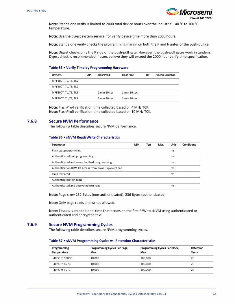
PolarFire FPGA
Microsemi Proprietary and Confidential. DS0141 Datasheet Revision 1.1 62
Note: Standalone verify is limited to 2000 total device hours over the industrial –40 °C to 100 °C temperature.
Note: Use the digest system service, for verify device time more than 2000 hours.
Note: Standalone verify checks the programming margin on both the P and N gates of the push-pull cell.
Note: Digest checks only the P side of the push-pull gate. However, the push-pull gates work in tandem. Digest check is recommended if users believe they will exceed the 2000 hour verify time specification.
Table 85 • Verify Time by Programming Hardware
Devices IAP FlashPro4 FlashPro5 BP Silicon Sculptor
MPF100T, TL, TS, TLS
MPF200T, TL, TS, TLS
MPF300T, TL, TS, TLS 1 min 50 sec 1 min 36 sec
MPF500T, TL, TS, TLS 2 min 40 sec 2 min 20 sec
Note: FlashPro4 verification time collected based on 4 MHz TCK. FlashPro5 verification time collected based on 10 MHz TCK.Note:
7.6.8 Secure NVM PerformanceThe following table describes secure NVM performance.
Table 86 • sNVM Read/Write Characteristics
Parameter Min Typ Max Unit Conditions
Plain text programming ms
Authenticated text programming ms
Authenticated and encrypted text programming ms
Authentication R/W 1st access from power-up overhead ms
Plain text read ms
Authenticated text read
Authenticated and decrypted text read ms
Note: Page size= 252 Bytes (non-authenticated), 236 Bytes (authenticated).
Note: Only page reads and writes allowed.
Note: T is an additional time that occurs on the first R/W to sNVM using authenticated or KEYOVHD
authenticated and encrypted text.
7.6.9 Secure NVM Programming CyclesThe following table describes secure NVM programming cycles.
Table 87 • sNVM Programming Cycles vs. Retention Characteristics
Programming Temperature
Programming Cycles Per Page, Max
Programming Cycles Per Block, Max
Retention Years
–40 °C to 100 °C 10,000 100,000 20
–40 °C to 85 °C 10,000 100,000 20
–40 °C to 55 °C 10,000 100,000 20
Note: Page size = 128 Bytes
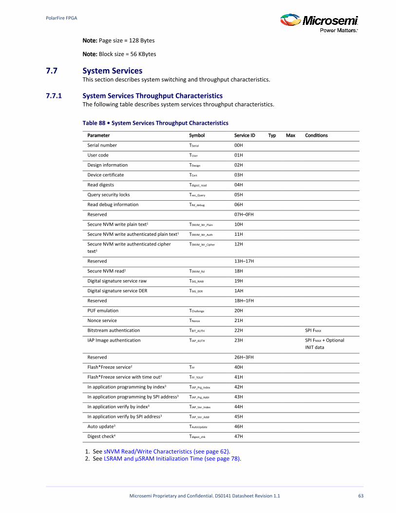
PolarFire FPGA
Microsemi Proprietary and Confidential. DS0141 Datasheet Revision 1.1 63
1. 2.
3.
Note: Page size = 128 Bytes
Note: Block size = 56 KBytes
7.7 System ServicesThis section describes system switching and throughput characteristics.
7.7.1 System Services Throughput CharacteristicsThe following table describes system services throughput characteristics.
Table 88 • System Services Throughput Characteristics
Parameter Symbol Service ID Typ Max Conditions
Serial number TSerial 00H
User code TUser 01H
Design information TDesign 02H
Device certificate TCert 03H
Read digests Tdigest_read 04H
Query security locks Tsec_Query 05H
Read debug information TRd_debug 06H
Reserved 07H–0FH
Secure NVM write plain text1 TSNVM_Wr_Plain 10H
Secure NVM write authenticated plain text1 TSNVM_Wr_Auth 11H
Secure NVM write authenticated cipher text1
TSNVM_Wr_Cipher 12H
Reserved 13H–17H
Secure NVM read1 TSNVM_Rd 18H
Digital signature service raw TSIG_RAW 19H
Digital signature service DER TSIG_DER 1AH
Reserved 1BH–1FH
PUF emulation TChallenge 20H
Nonce service TNonce 21H
Bitstream authentication TBIT_AUTH 22H SPI FMAX
IAP Image authentication TIAP_AUTH 23H SPI F + Optional MAX
INIT data
Reserved 26H–3FH
Flash*Freeze service2 TFF 40H
Flash*Freeze service with time out2 TFF_TOUT 41H
In application programming by index3 TIAP_Prg_Index 42H
In application programming by SPI address3 TIAP_Prg_Addr 43H
In application verify by index3 TIAP_Ver_Index 44H
In application verify by SPI address3 TIAP_Ver_Addr 45H
Auto update3 TAutoUpdate 46H
Digest check4 Tdigest_chk 47H
See .sNVM Read/Write Characteristics (see page 62)See .LSRAM and µSRAM Initialization Time (see page 78)
See .FPGA Programming Time (see page 57)
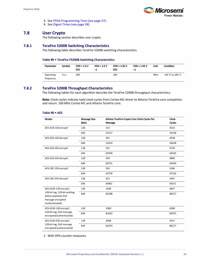
PolarFire FPGA
Microsemi Proprietary and Confidential. DS0141 Datasheet Revision 1.1 64
3. 4.
1.
See .FPGA Programming Time (see page 57)See .Digest Times (see page 58)
7.8 User CryptoThe following section describes user crypto.
7.8.1 TeraFire 5200B Switching CharacteristicsThe following table describes TeraFire 5200B switching characteristics.
Table 89 • TeraFire F5200B Switching Characteristics
Parameter Symbol VDD = 1.0 V STD
VDD = 1.0 V –1
VDD = 1.05 V STD
VDD = 1.05 V –1
Unit Condition
Operating frequency
FMAX 189 189 MHz –40 °C to 100 °C
7.8.2 TeraFire 5200B Throughput CharacteristicsThe following tables for each algorithm describe the TeraFire 5200B throughput characteristics.
Note: Clock-cycles indicate total clock-cycles from Cortex-M1 driver to Athena TeraFire core completion and return. 100 MHz Cortex-M1 and Athena TeraFire core.
Table 90 • AES
Modes Message Size (Bits)
Athena TeraFire Crypto Core Clock-Cycles Per Message
Clock-Cycles
AES-ECB-128 encrypt1 128 515 4523
64K 52157 56148
AES-ECB-128 decrypt1 128 561 4558
64K 52433 56428
AES-ECB-256 encrypt1 128 531 4730
64K 60349 64545
AES-ECB-256 decrypt1 128 593 4800
64K 60721 64930
AES-CBC-256 encrypt1 128 592 5366
64K 62739 67526
AES-CBC-256 decrypt1 128 621 5401
64K 60901 65671
AES-GCM-128 encrypt ,1
128-bit tag, 128-bit authtagbefore plaintext (full message encrypted/authenticated)
128 2506 6857
64K 82188 86517
AES-GCM-128 encrypt ,1
128-bit tag, (full messageencrypted/authenticated)
128 1960 6280
64K 81642 85975
AES-GCM-256 encrypt ,1
128-bit tag, (full messageencrypted/authenticated)
128 2008 6557
64K 81674 86217
With DPA counter measures.
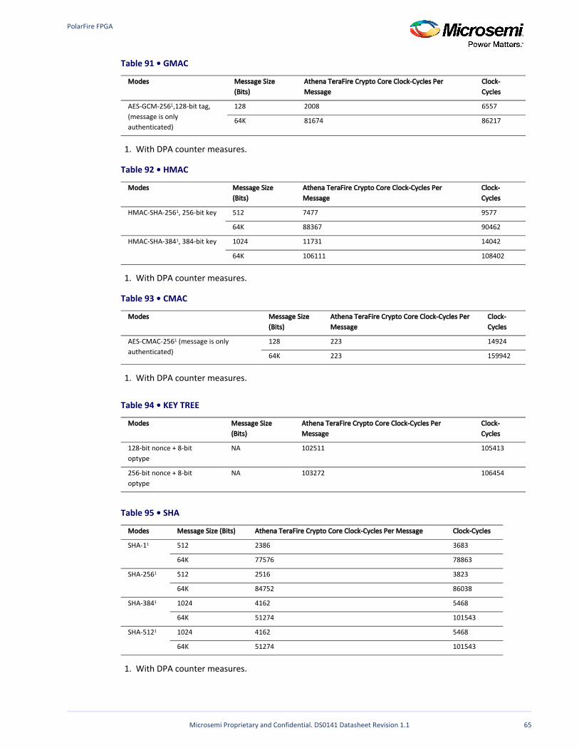
PolarFire FPGA
Microsemi Proprietary and Confidential. DS0141 Datasheet Revision 1.1 65
1.
1.
1.
1.
Table 91 • GMAC
Modes Message Size (Bits)
Athena TeraFire Crypto Core Clock-Cycles Per Message
Clock-Cycles
AES-GCM-256 ,128-bit tag,1
(message is only authenticated)
128 2008 6557
64K 81674 86217
With DPA counter measures.
Table 92 • HMAC
Modes Message Size (Bits)
Athena TeraFire Crypto Core Clock-Cycles Per Message
Clock-Cycles
HMAC-SHA-256 , 256-bit key1 512 7477 9577
64K 88367 90462
HMAC-SHA-384 , 384-bit key1 1024 11731 14042
64K 106111 108402
With DPA counter measures.
Table 93 • CMAC
Modes Message Size (Bits)
Athena TeraFire Crypto Core Clock-Cycles Per Message
Clock-Cycles
AES-CMAC-256 (message is only 1
authenticated)128 223 14924
64K 223 159942
With DPA counter measures.
Table 94 • KEY TREE
Modes Message Size (Bits)
Athena TeraFire Crypto Core Clock-Cycles Per Message
Clock-Cycles
128-bit nonce + 8-bit optype
NA 102511 105413
256-bit nonce + 8-bit optype
NA 103272 106454
Table 95 • SHA
Modes Message Size (Bits) Athena TeraFire Crypto Core Clock-Cycles Per Message Clock-Cycles
SHA-11 512 2386 3683
64K 77576 78863
SHA-2561 512 2516 3823
64K 84752 86038
SHA-3841 1024 4162 5468
64K 51274 101543
SHA-5121 1024 4162 5468
64K 51274 101543
With DPA counter measures.
PolarFire FPGA
Microsemi Proprietary and Confidential. DS0141 Datasheet Revision 1.1 66
1.
1.
Table 96 • ECC
Modes Message Size (Bits)
Athena TeraFire Crypto Core Clock-Cycles Per Message
Clock-Cycles
ECDSA SigGen, P-384/SHA-3841
1024 12530673 12538712
8K 12545812 12553842
ECDSA SigGen, P-384/SHA-384
1024 5502580 5510607
ECDSA SigVer, P-384/SHA-384 1024 6329349 6336684
8K 6374140 6381484
Key agreement (KAS), P-3841 5037644 5043464
Point multiply, P-2561 5176445 5182129
Point multiply, P-3841 12048196 12055249
Point multiply, P-5211 26886848 26895584
Point addition, P-384 5049697 5056192
KeyGen (PKG), P-3841 12059342 12067938
KeyVer (PKV), P-3841
Point verification, P-384 5185 8214
With DPA counter measures.
Table 97 • IFC (RSA)
Modes Message Size (Bits)
Athena TeraFire Crypto Core Clock-Cycles Per Message
Clock-Cycles
Encrypt, RSA-2048, e=65537 2048 1694898 1707983
3072 3734115 3752628
Decrypt, RSA-2048 , CRT1 2048
Decrypt, RSA-3072 , CRT1 3072
Decrypt, RSA-4096 , CRT1 4096
Decrypt, RSA-8192 , CRT1 8192
Decrypt, RSA-3072, CRT 3072 38135488 38160269
SigGen, RSA-3072/SHA-384 , PKCS #1 V 1
1.51024
8K
SigGen, RSA-3072/SHA-384, PKCS #1, V 1.5
1024 13199641 147436351
8K 13210656 147447376
SigVer, RSA-3072/SHA-384, e = 65537, PKCS #1 V 1.5
1024 21574887 88701666
8K 21583957 88710731
SigVer, RSA-2048/SHA-256, e = 65537, PKCS #1 V 1.5
1024 26916920 26929701
8K 26931018 26943806
SigGen, RSA-3072/SHA-384, ANSI X9.31 1024 13148583 147385003
8K 13156661 147393088
SigVer, RSA-3072/SHA-384, e = 65537, ANSI X9.31
1024 21614156 88740653
8K 21632391 88758888
With DPA counter measures.
PolarFire FPGA
Microsemi Proprietary and Confidential. DS0141 Datasheet Revision 1.1 67
1.
Table 98 • FFC (DH)
Modes Message Size (Bits) Athena TeraFire Crypto Core Clock-Cycles Per Message Clock-Cycles
SigGen, DSA-3072/SHA-3842
1024 27948851 27966136
8K 27961233 27978526
SigGen, DSA-3072/SHA-384
1024 11951377 11967172
SigVer, DSA-3072/SHA-384
1024 24484509 24504278
8K 24950598 24970373
SigVer, DSA-2048/SHA-256
1024 10016686 10031188
8K 10008257 10022753
Key Agreement (KAS), DH-3072(p= 3072, security= 256)
12207595 12225892
Key Agreement (KAS), DH-3072(p= 3072, security=56)1
40537984 241882971
With DPA counter measures.
Table 99 • NRBG
Modes Message Size (Bits)
Athena TeraFire Crypto Core Clock-Cycles Per Message
Clock-Cycles
Instantiate: strength,s = 256, 384-bit nonce, 384-bit personalization string
0 757
Reseed: no additional input,s = 256
769 4630
Reseed: 384-bit additional input,s = 256
1490 6271
Generate: (no add’l input, no prediction resistance), s = 256
128 1909 3640
Generate: (no add’l input, no prediction resistance), s = 256
8K 12808 27125
Generate: (no add’l input), prediction resistance enabled,s = 256
128 6078 7817
Generate: (no add’l input), prediction resistance enabled,s = 256
8K 16977 31337
Generate: 384-bit add’l input, (no prediction resistance),s = 256
128 6064 8539
Generate: 384-bit add’l input, (no prediction resistance),s = 256
8K 16963 32024
Generate: (no add’l input, no prediction resistance), s = 256
128 7719 10196
8K 18618 33681
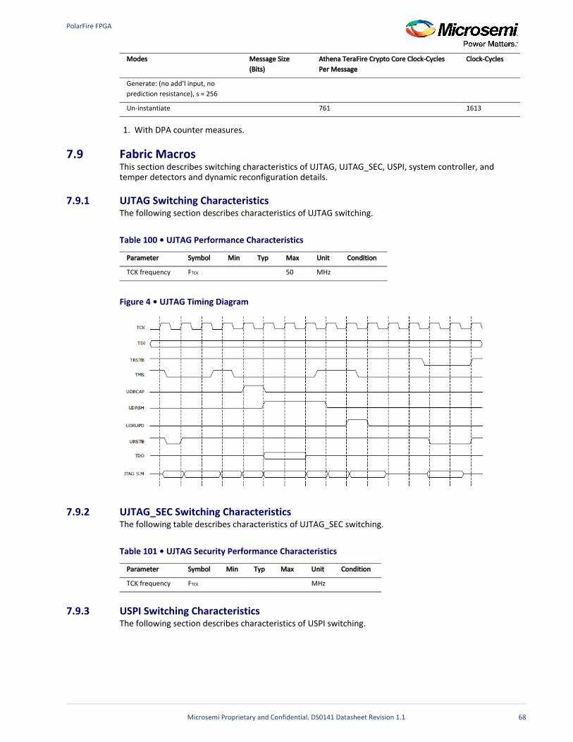
PolarFire FPGA
Microsemi Proprietary and Confidential. DS0141 Datasheet Revision 1.1 68
1.
Modes Message Size (Bits)
Athena TeraFire Crypto Core Clock-Cycles Per Message
Clock-Cycles
Generate: (no add’l input, no prediction resistance), s = 256
Un-instantiate 761 1613
With DPA counter measures.
7.9 Fabric MacrosThis section describes switching characteristics of UJTAG, UJTAG_SEC, USPI, system controller, and temper detectors and dynamic reconfiguration details.
7.9.1 UJTAG Switching CharacteristicsThe following section describes characteristics of UJTAG switching.
Table 100 • UJTAG Performance Characteristics
Parameter Symbol Min Typ Max Unit Condition
TCK frequency FTCK 50 MHz
Figure 4 • UJTAG Timing Diagram
7.9.2 UJTAG_SEC Switching CharacteristicsThe following table describes characteristics of UJTAG_SEC switching.
Table 101 • UJTAG Security Performance Characteristics
Parameter Symbol Min Typ Max Unit Condition
TCK frequency FTCK MHz
7.9.3 USPI Switching CharacteristicsThe following section describes characteristics of USPI switching.
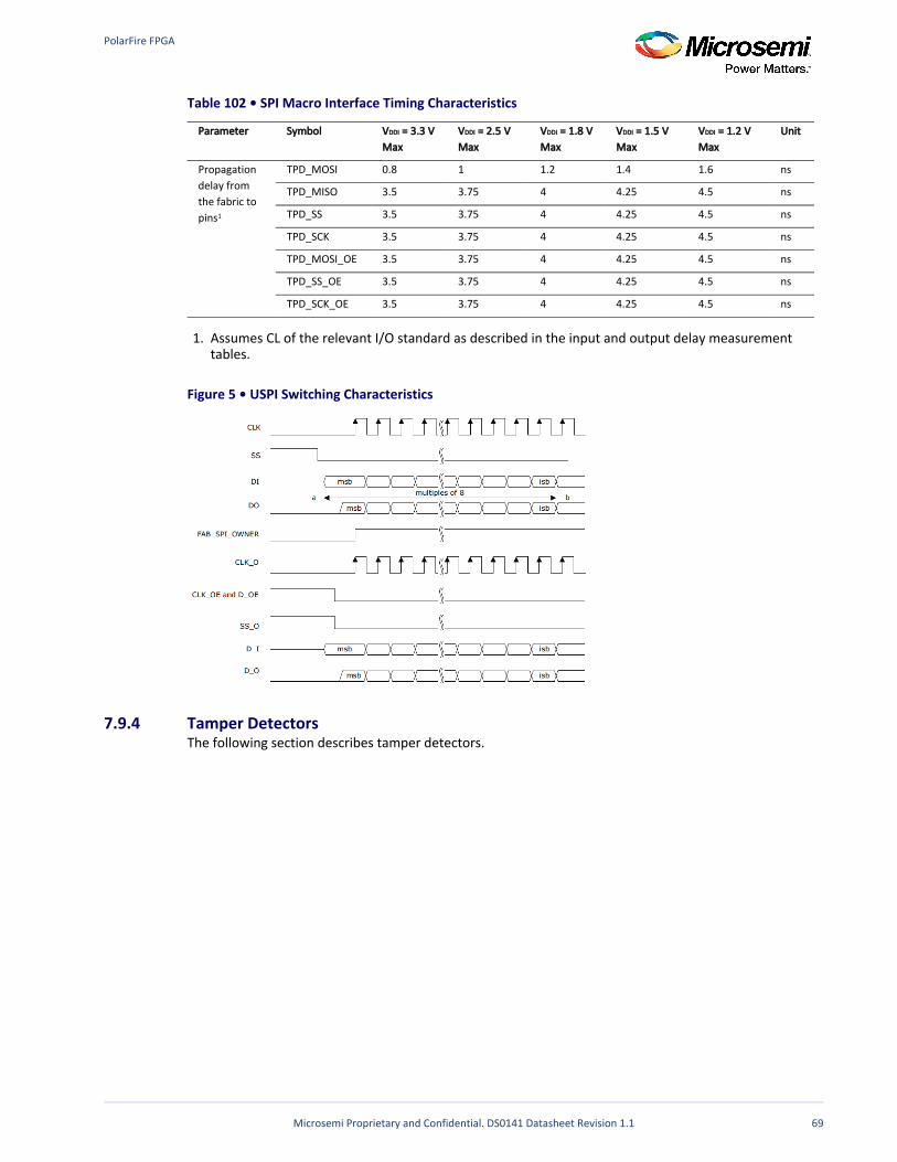
PolarFire FPGA
Microsemi Proprietary and Confidential. DS0141 Datasheet Revision 1.1 69
1.
Table 102 • SPI Macro Interface Timing Characteristics
Parameter Symbol V = 3.3 VDDI
MaxV = 2.5 VDDI Max
V = 1.8 VDDI Max
V = 1.5 VDDI Max
V = 1.2 VDDI Max
Unit
Propagation delay from the fabric to pins1
TPD_MOSI 0.8 1 1.2 1.4 1.6 ns
TPD_MISO 3.5 3.75 4 4.25 4.5 ns
TPD_SS 3.5 3.75 4 4.25 4.5 ns
TPD_SCK 3.5 3.75 4 4.25 4.5 ns
TPD_MOSI_OE 3.5 3.75 4 4.25 4.5 ns
TPD_SS_OE 3.5 3.75 4 4.25 4.5 ns
TPD_SCK_OE 3.5 3.75 4 4.25 4.5 ns
Assumes CL of the relevant I/O standard as described in the input and output delay measurement tables.
Figure 5 • USPI Switching Characteristics
7.9.4 Tamper DetectorsThe following section describes tamper detectors.
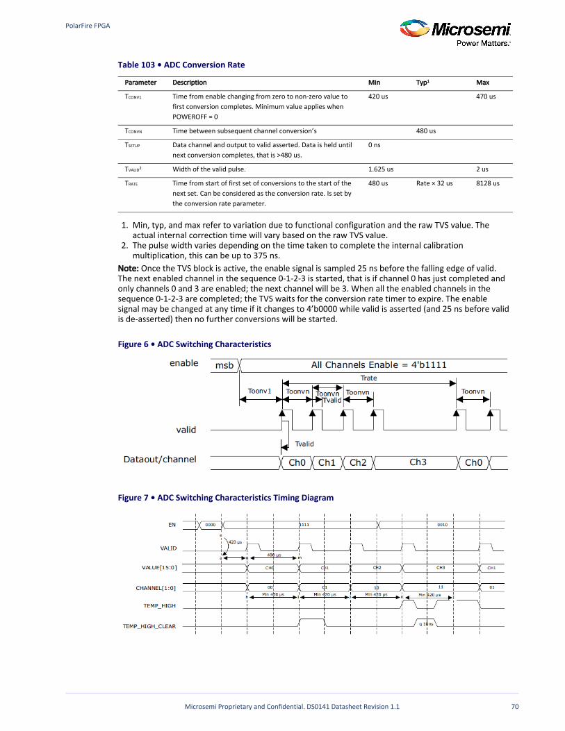
PolarFire FPGA
Microsemi Proprietary and Confidential. DS0141 Datasheet Revision 1.1 70
1.
2.
Table 103 • ADC Conversion Rate
Parameter Description Min Typ1 Max
TCONV1 Time from enable changing from zero to non-zero value to first conversion completes. Minimum value applies when POWEROFF = 0
420 us 470 us
TCONVN Time between subsequent channel conversion’s 480 us
TSETUP Data channel and output to valid asserted. Data is held until next conversion completes, that is >480 us.
0 ns
TVALID2 Width of the valid pulse. 1.625 us 2 us
TRATE Time from start of first set of conversions to the start of the next set. Can be considered as the conversion rate. Is set by the conversion rate parameter.
480 us Rate × 32 us 8128 us
Min, typ, and max refer to variation due to functional configuration and the raw TVS value. The actual internal correction time will vary based on the raw TVS value.The pulse width varies depending on the time taken to complete the internal calibration multiplication, this can be up to 375 ns.
Note: Once the TVS block is active, the enable signal is sampled 25 ns before the falling edge of valid. The next enabled channel in the sequence 0-1-2-3 is started, that is if channel 0 has just completed and only channels 0 and 3 are enabled; the next channel will be 3. When all the enabled channels in the sequence 0-1-2-3 are completed; the TVS waits for the conversion rate timer to expire. The enable signal may be changed at any time if it changes to 4’b0000 while valid is asserted (and 25 ns before valid is de-asserted) then no further conversions will be started.
Figure 6 • ADC Switching Characteristics
Figure 7 • ADC Switching Characteristics Timing Diagram
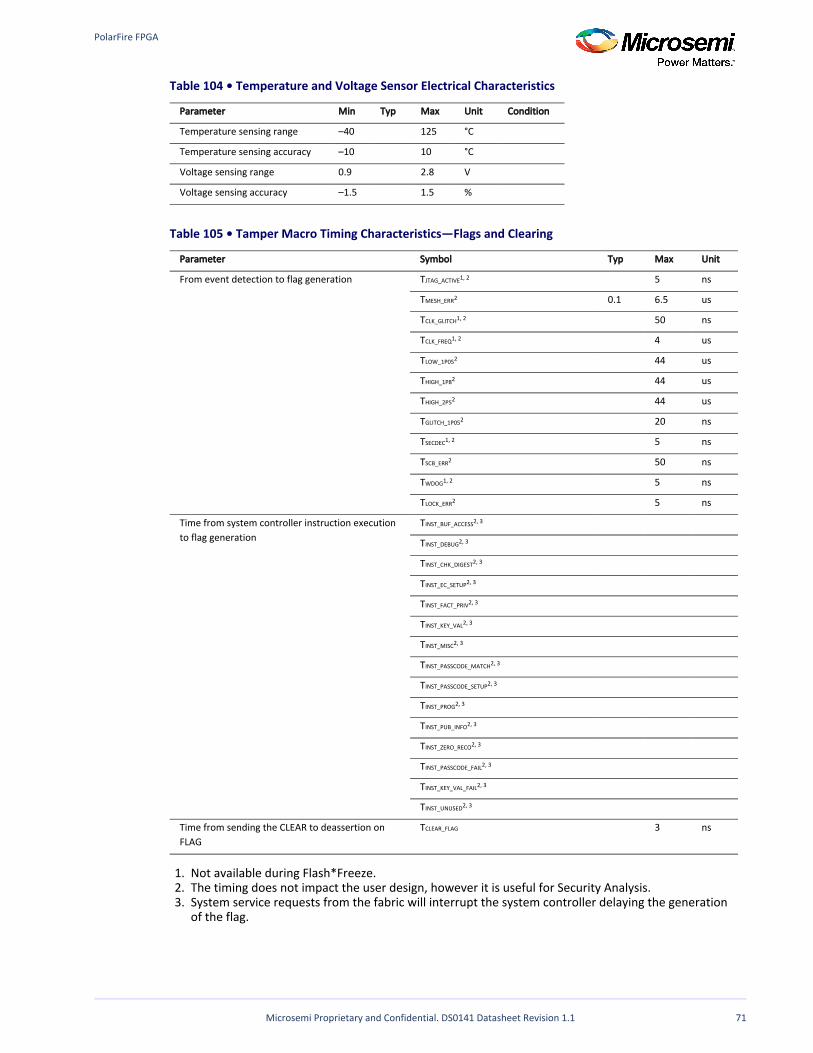
PolarFire FPGA
Microsemi Proprietary and Confidential. DS0141 Datasheet Revision 1.1 71
1. 2. 3.
Table 104 • Temperature and Voltage Sensor Electrical Characteristics
Parameter Min Typ Max Unit Condition
Temperature sensing range –40 125 °C
Temperature sensing accuracy –10 10 °C
Voltage sensing range 0.9 2.8 V
Voltage sensing accuracy –1.5 1.5 %
Table 105 • Tamper Macro Timing Characteristics—Flags and Clearing
Parameter Symbol Typ Max Unit
From event detection to flag generation TJTAG_ACTIVE1, 2 5 ns
TMESH_ERR2 0.1 6.5 us
TCLK_GLITCH1, 2 50 ns
TCLK_FREQ1, 2 4 us
TLOW_1P052 44 us
THIGH_1P82 44 us
THIGH_2P52 44 us
TGLITCH_1P052 20 ns
TSECDEC1, 2 5 ns
TSCB_ERR2 50 ns
TWDOG1, 2 5 ns
TLOCK_ERR2 5 ns
Time from system controller instruction execution to flag generation
TINST_BUF_ACCESS2, 3
TINST_DEBUG2, 3
TINST_CHK_DIGEST2, 3
TINST_EC_SETUP2, 3
TINST_FACT_PRIV2, 3
TINST_KEY_VAL2, 3
TINST_MISC2, 3
TINST_PASSCODE_MATCH2, 3
TINST_PASSCODE_SETUP2, 3
TINST_PROG2, 3
TINST_PUB_INFO2, 3
TINST_ZERO_RECO2, 3
TINST_PASSCODE_FAIL2, 3
TINST_KEY_VAL_FAIL2, 3
TINST_UNUSED2, 3
Time from sending the CLEAR to deassertion on FLAG
TCLEAR_FLAG 3 ns
Not available during Flash*Freeze.The timing does not impact the user design, however it is useful for Security Analysis.System service requests from the fabric will interrupt the system controller delaying the generation of the flag.
PolarFire FPGA
Microsemi Proprietary and Confidential. DS0141 Datasheet Revision 1.1 72
1.
2.
Table 106 • Tamper Macro Response Timing Characteristics
Parameter Symbol Typ Max Unit
Time from triggering the response to all I/Os disabled TIO_DISABLE 150 ns
Time from negation of RESPONSE to all I/Os re-enabled TCLR_IO_DISABLE 10 us
Time from triggering the response to security locked TLOCKDOWN 20 ns
Time from negation of RESPONSE to earlier security unlock condition TCLR_LOCKDOWN 20 ns
Time from triggering the response to device enters RESET Ttr_RESET
Time from triggering the response to start of zeroization Ttr_ZEROLISE
7.9.5 System Controller Suspend Switching CharacteristicsThe following table describes the characteristics of system controller suspend switching.
Table 107 • System Controller Suspend Entry and Exit Characteristics
Parameter Symbol Definition Typ Max Unit
Time from TRSTb falling edge to SUSPEND_EN signal assertion
Tsuspend_Tr1, 2 Suspend entry time from TRST_N assertion
1 µs
Time from TRSTb rising edge to ACTIVE signal assertion
Tsuspend_exit Suspend exit time fromTRST_N negation
360 µs
ACTIVE indicates that the system controller is inactive or active regardless of the state of SUSPEND_EN.ACTIVE signal must never be asserted with SUSPEND_EN is asserted.
7.9.6 Dynamic Reconfiguration InterfaceThe following table provides interface timing information for the DRI, which is an embedded APB slave interface within the FPGA fabric that does not use FPGA resources.
Table 108 • Dynamic Reconfiguration Interface Timing Characteristics
Parameter Symbol Max Unit
PCLK frequency FPD _PCLK 200 MHz
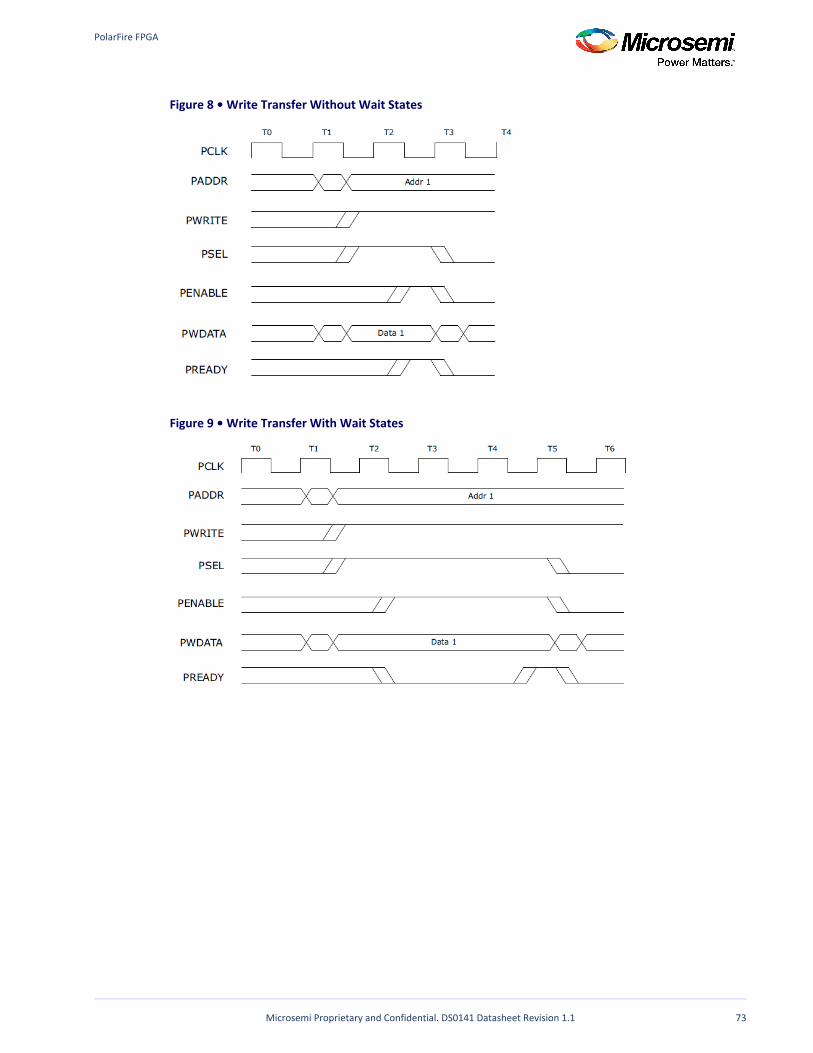
PolarFire FPGA
Microsemi Proprietary and Confidential. DS0141 Datasheet Revision 1.1 73
Figure 8 • Write Transfer Without Wait States
Figure 9 • Write Transfer With Wait States
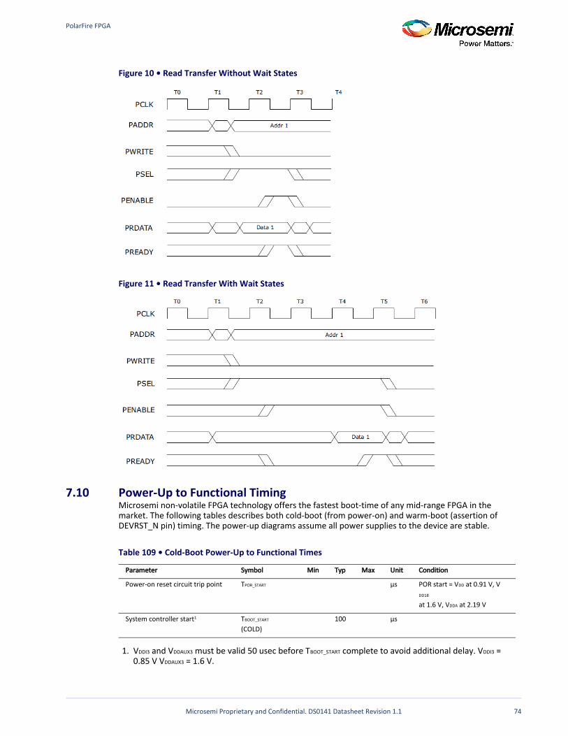
PolarFire FPGA
Microsemi Proprietary and Confidential. DS0141 Datasheet Revision 1.1 74
1.
Figure 10 • Read Transfer Without Wait States
Figure 11 • Read Transfer With Wait States
7.10 Power-Up to Functional TimingMicrosemi non-volatile FPGA technology offers the fastest boot-time of any mid-range FPGA in the market. The following tables describes both cold-boot (from power-on) and warm-boot (assertion of DEVRST_N pin) timing. The power-up diagrams assume all power supplies to the device are stable.
Table 109 • Cold-Boot Power-Up to Functional Times
Parameter Symbol Min Typ Max Unit Condition
Power-on reset circuit trip point TPOR_START µs POR start = V at 0.91 V, VDD
DD18
at 1.6 V, V at 2.19 VDDA
System controller start1 T BOOT_START
(COLD) 100 µs
V and V must be valid 50 usec before T complete to avoid additional delay. V = DDI3 DDAUX3 BOOT_START DDI3
0.85 V V = 1.6 V.DDAUX3
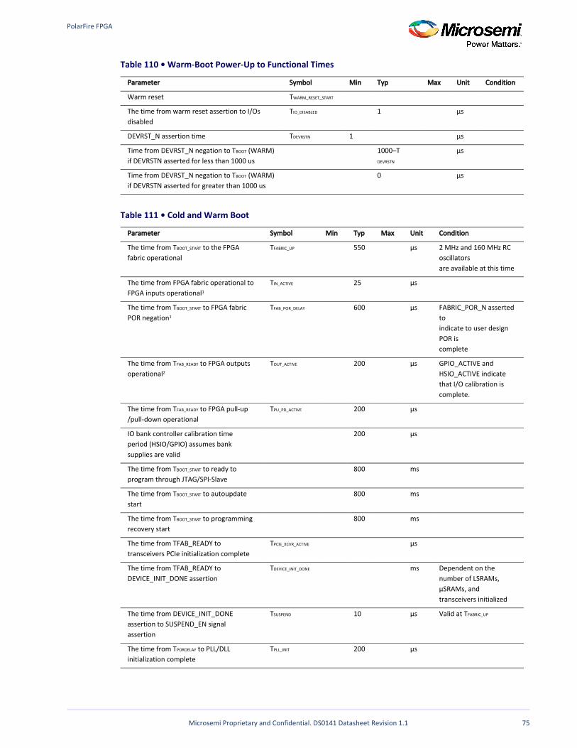
PolarFire FPGA
Microsemi Proprietary and Confidential. DS0141 Datasheet Revision 1.1 75
Table 110 • Warm-Boot Power-Up to Functional Times
Parameter Symbol Min Typ Max Unit Condition
Warm reset TWARM_RESET_START
The time from warm reset assertion to I/Os disabled
TIO_DISABLED 1 µs
DEVRST_N assertion time TDEVRSTN 1 µs
Time from DEVRST_N negation to T (WARM)BOOT
if DEVRSTN asserted for less than 1000 us 1000–T
DEVRSTN
µs
Time from DEVRST_N negation to T (WARM)BOOT
if DEVRSTN asserted for greater than 1000 us 0 µs
Table 111 • Cold and Warm Boot
Parameter Symbol Min Typ Max Unit Condition
The time from T to the FPGA BOOT_START
fabric operationalTFABRIC_UP 550 µs 2 MHz and 160 MHz RC
oscillatorsare available at this time
The time from FPGA fabric operational to FPGA inputs operational1
TIN_ACTIVE 25 µs
The time from T to FPGA fabric BOOT_START
POR negation1
TFAB_POR_DELAY 600 µs FABRIC_POR_N asserted toindicate to user design POR iscomplete
The time from T to FPGA outputs FAB_READY
operational2
TOUT_ACTIVE 200 µs GPIO_ACTIVE and HSIO_ACTIVE indicate that I/O calibration is complete.
The time from T to FPGA pull-upFAB_READY
/pull-down operationalTPU_PD_ACTIVE 200 µs
IO bank controller calibration time period (HSIO/GPIO) assumes bank supplies are valid
200 µs
The time from T to ready to BOOT_START
program through JTAG/SPI-Slave 800 ms
The time from T to autoupdate BOOT_START
start 800 ms
The time from T to programming BOOT_START
recovery start 800 ms
The time from TFAB_READY to transceivers PCIe initialization complete
TPCIE_XCVR_ACTIVE μs
The time from TFAB_READY to DEVICE_INIT_DONE assertion
TDEVICE_INIT_DONE ms Dependent on the number of LSRAMs, μSRAMs, and transceivers initialized
The time from DEVICE_INIT_DONEassertion to SUSPEND_EN signal assertion
TSUSPEND 10 μs Valid at TFABRIC_UP
The time from T to PLL/DLL PORDELAY
initialization completeTPLL_INIT 200 μs
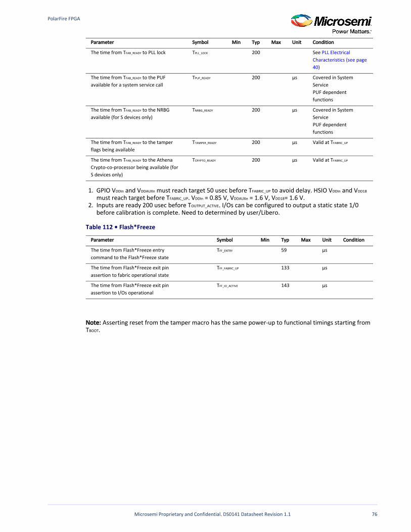
PolarFire FPGA
Microsemi Proprietary and Confidential. DS0141 Datasheet Revision 1.1 76
1.
2.
Parameter Symbol Min Typ Max Unit Condition
The time from T to PLL lockFAB_READY TPLL_LOCK 200 See PLL Electrical Characteristics (see page 40)
The time from T to the PUF FAB_READY
available for a system service callTPUF_READY 200 μs Covered in System
ServicePUF dependent functions
The time from T to the NRBG FAB_READY
available (for S devices only)TNRBG_READY 200 μs Covered in System
ServicePUF dependent functions
The time from T to the tamper FAB_READY
flags being availableTTAMPER_READY 200 μs Valid at TFABRIC_UP
The time from T to the Athena FAB_READY
Crypto-co-processor being available (for S devices only)
TCRYPTO_READY 200 μs Valid at TFABRIC_UP
GPIO V and V must reach target 50 usec before T to avoid delay. HSIO V and V DDIn DDAUXn FABRIC_UP DDIn DD18
must reach target before T . V = 0.85 V, V = 1.6 V, V = 1.6 V.FABRIC_UP DDIn DDAUXn DD18
Inputs are ready 200 usec before T . I/Os can be configured to output a static state 1/0 OUTPUT_ACTIVE
before calibration is complete. Need to determined by user/Libero.
Table 112 • Flash*Freeze
Parameter Symbol Min Typ Max Unit Condition
The time from Flash*Freeze entrycommand to the Flash*Freeze state
TFF_ENTRY 59 μs
The time from Flash*Freeze exit pinassertion to fabric operational state
TFF_FABRIC_UP 133 μs
The time from Flash*Freeze exit pinassertion to I/Os operational
TFF_IO_ACTIVE 143 μs
Note: Asserting reset from the tamper macro has the same power-up to functional timings starting from T .BOOT
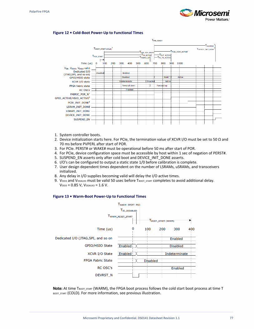
PolarFire FPGA
Microsemi Proprietary and Confidential. DS0141 Datasheet Revision 1.1 77
1. 2.
3. 4. 5. 6. 7.
8. 9.
Figure 12 • Cold-Boot Power-Up to Functional Times
System controller boots.Device initialization starts here. For PCIe, the termination value of XCVR I/O must be set to 50 Ω and 70 ms before PVPERL after start of POR.For PCIe. PERST# or WAKE# must be operational before 50 ms after start of POR.For PCIe, device configuration space must be accessible by host within 1 sec of negation of PERST#.SUSPEND_EN asserts only after cold boot and DEVICE_INIT_DONE asserts.I/O's can be configured to output a static state 1/0 before calibration is complete.User design dependent times dependent on the number of LSRAMs, uSRAMs, and transceivers initialized.Any delay in I/O supplies becoming valid will delay the I/O active times.V and V must be valid 50 usec before T completes to avoid additional delay.DDI3 DDAUX3 BOOT_START
V = 0.85 V, V = 1.6 V.DDI3 DDAUX3
Figure 13 • Warm-Boot Power-Up to Functional Times
Note: At time T (WARM), the FPGA boot process follows the cold start boot process at time TBOOT_START
(COLD). For more information, see previous illustration.BOOT_START
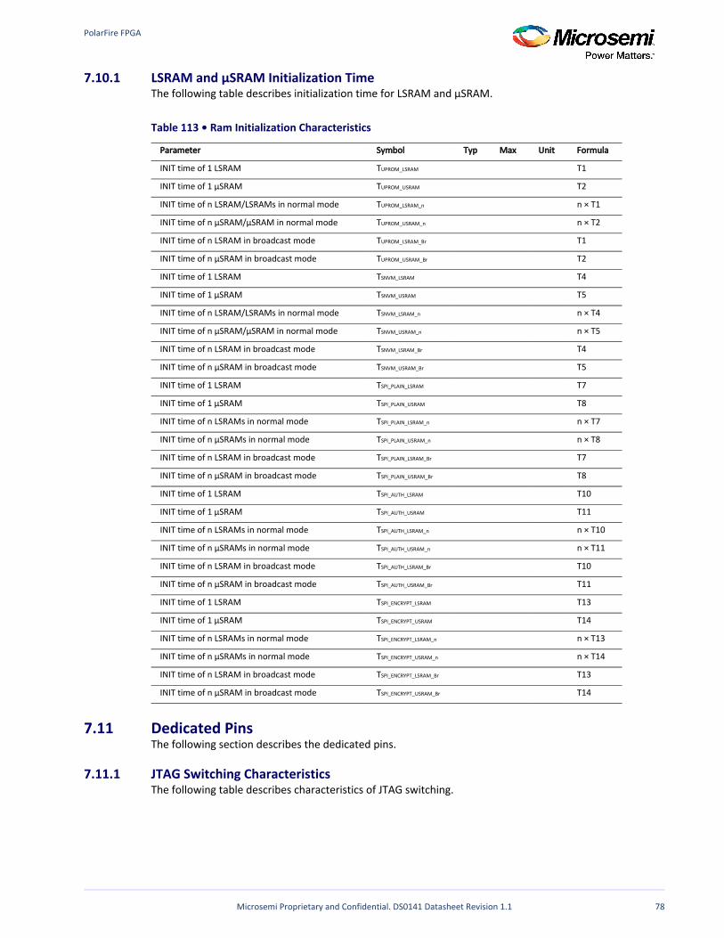
PolarFire FPGA
Microsemi Proprietary and Confidential. DS0141 Datasheet Revision 1.1 78
7.10.1 LSRAM and μSRAM Initialization TimeThe following table describes initialization time for LSRAM and μSRAM.
Table 113 • Ram Initialization Characteristics
Parameter Symbol Typ Max Unit Formula
INIT time of 1 LSRAM TUPROM_LSRAM T1
INIT time of 1 µSRAM TUPROM_USRAM T2
INIT time of n LSRAM/LSRAMs in normal mode TUPROM_LSRAM_n n × T1
INIT time of n µSRAM/µSRAM in normal mode TUPROM_USRAM_n n × T2
INIT time of n LSRAM in broadcast mode TUPROM_LSRAM_Br T1
INIT time of n µSRAM in broadcast mode TUPROM_USRAM_Br T2
INIT time of 1 LSRAM TSNVM_LSRAM T4
INIT time of 1 µSRAM TSNVM_USRAM T5
INIT time of n LSRAM/LSRAMs in normal mode TSNVM_LSRAM_n n × T4
INIT time of n µSRAM/µSRAM in normal mode TSNVM_USRAM_n n × T5
INIT time of n LSRAM in broadcast mode TSNVM_LSRAM_Br T4
INIT time of n µSRAM in broadcast mode TSNVM_USRAM_Br T5
INIT time of 1 LSRAM TSPI_PLAIN_LSRAM T7
INIT time of 1 µSRAM TSPI_PLAIN_USRAM T8
INIT time of n LSRAMs in normal mode TSPI_PLAIN_LSRAM_n n × T7
INIT time of n µSRAMs in normal mode TSPI_PLAIN_USRAM_n n × T8
INIT time of n LSRAM in broadcast mode TSPI_PLAIN_LSRAM_Br T7
INIT time of n µSRAM in broadcast mode TSPI_PLAIN_USRAM_Br T8
INIT time of 1 LSRAM TSPI_AUTH_LSRAM T10
INIT time of 1 µSRAM TSPI_AUTH_USRAM T11
INIT time of n LSRAMs in normal mode TSPI_AUTH_LSRAM_n n × T10
INIT time of n µSRAMs in normal mode TSPI_AUTH_USRAM_n n × T11
INIT time of n LSRAM in broadcast mode TSPI_AUTH_LSRAM_Br T10
INIT time of n µSRAM in broadcast mode TSPI_AUTH_USRAM_Br T11
INIT time of 1 LSRAM TSPI_ENCRYPT_LSRAM T13
INIT time of 1 µSRAM TSPI_ENCRYPT_USRAM T14
INIT time of n LSRAMs in normal mode TSPI_ENCRYPT_LSRAM_n n × T13
INIT time of n µSRAMs in normal mode TSPI_ENCRYPT_USRAM_n n × T14
INIT time of n LSRAM in broadcast mode TSPI_ENCRYPT_LSRAM_Br T13
INIT time of n µSRAM in broadcast mode TSPI_ENCRYPT_USRAM_Br T14
7.11 Dedicated PinsThe following section describes the dedicated pins.
7.11.1 JTAG Switching CharacteristicsThe following table describes characteristics of JTAG switching.
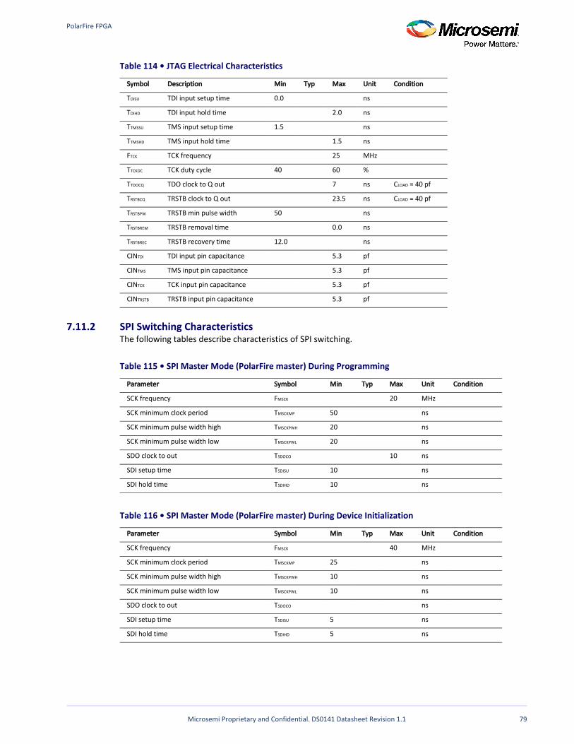
PolarFire FPGA
Microsemi Proprietary and Confidential. DS0141 Datasheet Revision 1.1 79
Table 114 • JTAG Electrical Characteristics
Symbol Description Min Typ Max Unit Condition
TDISU TDI input setup time 0.0 ns
TDIHD TDI input hold time 2.0 ns
TTMSSU TMS input setup time 1.5 ns
TTMSHD TMS input hold time 1.5 ns
FTCK TCK frequency 25 MHz
TTCKDC TCK duty cycle 40 60 %
TTDOCQ TDO clock to Q out 7 ns C = 40 pfLOAD
TRSTBCQ TRSTB clock to Q out 23.5 ns C = 40 pfLOAD
TRSTBPW TRSTB min pulse width 50 ns
TRSTBREM TRSTB removal time 0.0 ns
TRSTBREC TRSTB recovery time 12.0 ns
CINTDI TDI input pin capacitance 5.3 pf
CINTMS TMS input pin capacitance 5.3 pf
CINTCK TCK input pin capacitance 5.3 pf
CINTRSTB TRSTB input pin capacitance 5.3 pf
7.11.2 SPI Switching CharacteristicsThe following tables describe characteristics of SPI switching.
Table 115 • SPI Master Mode (PolarFire master) During Programming
Parameter Symbol Min Typ Max Unit Condition
SCK frequency FMSCK 20 MHz
SCK minimum clock period TMSCKMP 50 ns
SCK minimum pulse width high TMSCKPWH 20 ns
SCK minimum pulse width low TMSCKPWL 20 ns
SDO clock to out TSDOCO 10 ns
SDI setup time TSDISU 10 ns
SDI hold time TSDIHD 10 ns
Table 116 • SPI Master Mode (PolarFire master) During Device Initialization
Parameter Symbol Min Typ Max Unit Condition
SCK frequency FMSCK 40 MHz
SCK minimum clock period TMSCKMP 25 ns
SCK minimum pulse width high TMSCKPWH 10 ns
SCK minimum pulse width low TMSCKPWL 10 ns
SDO clock to out TSDOCO ns
SDI setup time TSDISU 5 ns
SDI hold time TSDIHD 5 ns
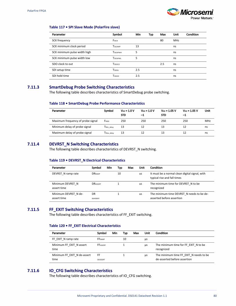
PolarFire FPGA
Microsemi Proprietary and Confidential. DS0141 Datasheet Revision 1.1 80
Table 117 • SPI Slave Mode (PolarFire slave)
Parameter Symbol Min Typ Max Unit Condition
SCK frequency FSSCK 80 MHz
SCK minimum clock period TSSCKMP 13 ns
SCK minimum pulse width high TSSCKPWH 5 ns
SCK minimum pulse width low TSSCKPWL 5 ns
SDO clock to out TSDOCO 2.5 ns
SDI setup time TSDISU 2.5 ns
SDI hold time TSDIHD 2.5 ns
7.11.3 SmartDebug Probe Switching CharacteristicsThe following table describes characteristics of SmartDebug probe switching.
Table 118 • SmartDebug Probe Performance Characteristics
Parameter Symbol V = 1.0 VDD
STD V = 1.0 VDD
–1 V = 1.05 VDD
STD V = 1.05 VDD
–1Unit
Maximum frequency of probe signal FMAX 250 250 250 250 MHz
Minimum delay of probe signal TMin_delay 13 12 13 12 ns
Maximum delay of probe signal TMax_delay 13 12 13 12 ns
7.11.4 DEVRST_N Switching CharacteristicsThe following table describes characteristics of DEVRST_N switching.
Table 119 • DEVRST_N Electrical Characteristics
Parameter Symbol Min Typ Max Unit Condition
DEVRST_N ramp rate DRRAMP 10 us It must be a normal clean digital signal, with typical rise and fall times
Minimum DEVRST_N assert time
DRASSERT 1 us The minimum time for DEVRST_N to be recognized
Minimum DEVRST_N de-assert time
DRDEASSERT
1 us The minimum time DEVRST_N needs to be de-asserted before assertion
7.11.5 FF_EXIT Switching CharacteristicsThe following table describes characteristics of FF_EXIT switching.
Table 120 • FF_EXIT Electrical Characteristics
Parameter Symbol Min Typ Max Unit Condition
FF_EXIT_N ramp rate FFRAMP 10 µs
Minimum FF_EXIT_N assert time
FFASSERT 1 µs The minimum time for FF_EXIT_N to be recognized
Minimum FF_EXIT_N de-assert time
FFDEASSERT
1 µs The minimum time FF_EXIT_N needs to be de-asserted before assertion
7.11.6 IO_CFG Switching CharacteristicsThe following table describes characteristics of IO_CFG switching.
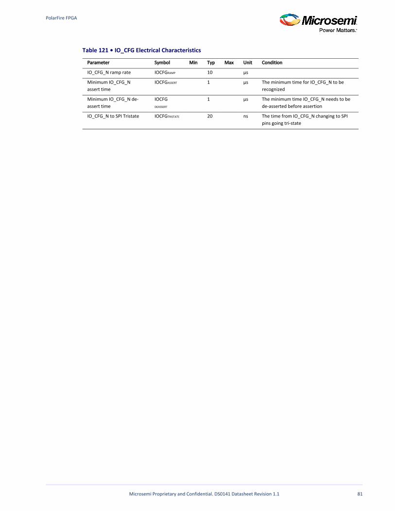
PolarFire FPGA
Microsemi Proprietary and Confidential. DS0141 Datasheet Revision 1.1 81
Table 121 • IO_CFG Electrical Characteristics
Parameter Symbol Min Typ Max Unit Condition
IO_CFG_N ramp rate IOCFGRAMP 10 µs
Minimum IO_CFG_N assert time
IOCFGASSERT 1 µs The minimum time for IO_CFG_N to be recognized
Minimum IO_CFG_N de-assert time
IOCFGDEASSERT
1 µs The minimum time IO_CFG_N needs to be de-asserted before assertion
IO_CFG_N to SPI Tristate IOCFGTRISTATE 20 ns The time from IO_CFG_N changing to SPI pins going tri-state
PolarFire FPGA
Microsemi Proprietary and Confidential. DS0141 Datasheet Revision 1.1 82
Microsemi Corporate HeadquartersOne Enterprise, Aliso Viejo,CA 92656 USAWithin the USA: +1 (800) 713-4113Outside the USA: +1 (949) 380-6100Fax: +1 (949) 215-4996Email: [email protected]
© 2017 Microsemi Corporation. All rights reserved. Microsemi and the Microsemi logo are trademarks of Microsemi Corporation. All other trademarks and service marks are the property of their respective owners.
Microsemi makes no warranty, representation, or guarantee regarding the information contained herein or the suitability of its products and services for any particular purpose, nor does Microsemi assume any liability whatsoever arising out of the application or use of any product or circuit. The products sold hereunder and any other products sold by Microsemi have been subject to limited testing and should not be used in conjunction with mission-critical equipment or applications. Any performance specifications are believed to be reliable but are not verified, and Buyer must conduct and complete all performance and other testing of the products, alone and together with, or installed in, any end-products. Buyer shall not rely on any data and performance specifications or parameters provided by Microsemi. It is the Buyer's responsibility to independently determine suitability of any products and to test and verify the same. The information provided by Microsemi hereunder is provided "as is, where is" and with all faults, and the entire risk associated with such information is entirely with the Buyer. Microsemi does not grant, explicitly or implicitly, to any party any patent rights, licenses, or any other IP rights, whether with regard to such information itself or anything described by such information. Information provided in this document is proprietary to Microsemi, and Microsemi reserves the right to make any changes to the information in this document or to any products and services at any time without notice.
Microsemi Corporation (Nasdaq: MSCC) offers a comprehensive portfolio of semiconductor and system solutions for aerospace & defense, communications, data center and industrial markets. Products include high-performance and radiation-hardened analog mixed-signal integrated circuits, FPGAs, SoCs and ASICs; power management products; timing and synchronization devices and precise time solutions, setting the world's standard for time; voice processing devices; RF solutions; discrete components; enterprise storage and communication solutions; security technologies and scalable anti-tamper products; Ethernet solutions; Power-over-Ethernet ICs and midspans; as well as custom design capabilities and services. Microsemi is headquartered in Aliso Viejo, California, and has approximately 4,800 employees globally. Learn more at www.microsemi.com.
51700141