2016.06.21 gmm csic NanoFrontMag
49
MAGNETIC NANO & MICRO WIRES Manuel Vazquez Group of Magnetic Wires . Institute of Materials Science of Madrid, CSIC. Spain 1.5 mm metallic diameter
-
Upload
nanofrontmag-cm -
Category
Science
-
view
112 -
download
3
Transcript of 2016.06.21 gmm csic NanoFrontMag
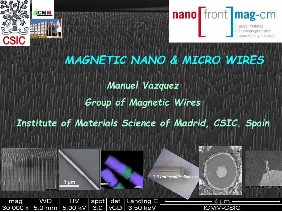
MAGNETIC NANO & MICRO WIRES
Manuel Vazquez
Group of Magnetic Wires .
Institute of Materials Science of Madrid, CSIC. Spain
1.5 mm metallic diameter
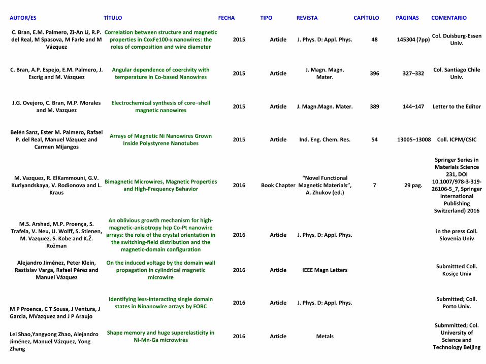
AUTOR/ES TÍTULO FECHA TIPO REVISTA CAPÍTULO PÁGINAS COMENTARIO
C. Bran, E.M. Palmero, Zi-An Li, R.P. del Real, M Spasova, M Farle and M
Vázquez
Correlation between structure and magnetic properties in CoxFe100-x nanowires: the roles of composition and wire diameter
2015 Article J. Phys. D: Appl. Phys. 48 145304 (7pp) Col. Duisburg-Essen
Univ.
C. Bran, A.P. Espejo, E.M. Palmero, J. Escrig and M. Vázquez
Angular dependence of coercivity with temperature in Co-based Nanowires
2015 Article J. Magn. Magn.
Mater. 396 327–332
Col. Santiago Chile Univ.
J.G. Ovejero, C. Bran, M.P. Morales and M. Vazquez
Electrochemical synthesis of core–shell magnetic nanowires
2015 Article J. Magn.Magn. Mater. 389 144–147 Letter to the Editor
Belen Sanz, Ester M. Palmero, Rafael P. del Real, Manuel Vazquez and
Carmen Mijangos
Arrays of Magnetic Ni Nanowires Grown Inside Polystyrene Nanotubes
2015 Article Ind. Eng. Chem. Res. 54 13005−13008 Coll. ICPM/CSIC
M. Vazquez, R. ElKammouni, G.V. Kurlyandskaya, V. Rodionova and L.
Kraus
Bimagnetic Microwires, Magnetic Properties and High-Frequency Behavior
2016 Book Chapter “Novel Functional
Magnetic Materials”, A. Zhukov (ed.)
7 29 pag.
Springer Series in Materials Science
231, DOI 10.1007/978-3-319-26106-5_7, Springer
International Publishing
Switzerland) 2016
M.S. Arshad, M.P. Proença, S. Trafela, V. Neu, U. Wolff, S. Stienen,
M. Vazquez, S. Kobe and K.Ž. Rožman
An oblivious growth mechanism for high-magnetic-anisotropy hcp Co-Pt nanowire
arrays: the role of the crystal orientation in the switching-field distribution and the
magnetic-domain configuration
2016 Article J. Phys. D: Appl. Phys. in the press Coll.
Slovenia Univ
Alejandro Jiménez, Peter Klein, Rastislav Varga, Rafael Pérez and
Manuel Vázquez
On the induced voltage by the domain wall propagation in cylindrical magnetic
microwire 2016 Article IEEE Magn Letters
Submittted Coll. Kosiçe Univ
M P Proenca, C T Sousa, J Ventura, J Garcia, MVazquez and J P Araujo
Identifying less-interacting single domain states in Ninanowire arrays by FORC
2016 Article J. Phys. D: Appl. Phys. Submitted; Coll.
Porto Univ.
Lei Shao,Yangyong Zhao, Alejandro Jiménez, Manuel Vázquez, Yong Zhang
Shape memory and huge superelasticity in Ni-Mn-Ga microwires
2016 Article Metals
Submmitted; Col. University of Science and
Technology Beijing
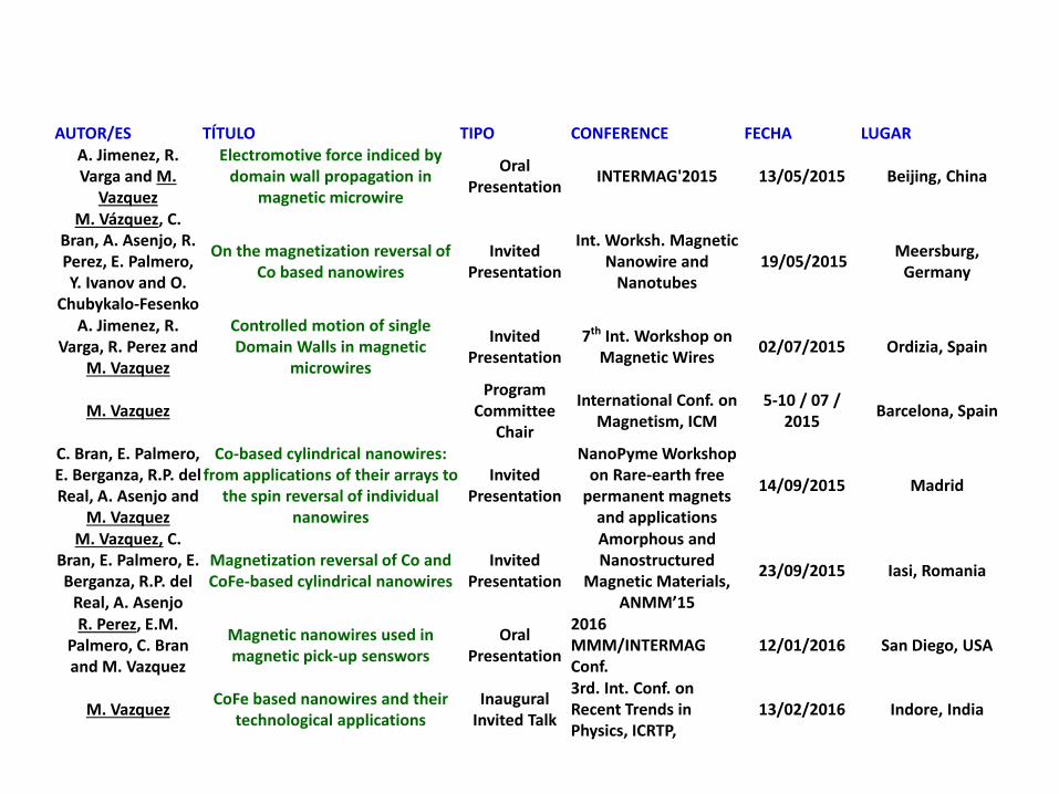
AUTOR/ES TÍTULO TIPO CONFERENCE FECHA LUGAR A. Jimenez, R. Varga and M.
Vazquez
Electromotive force indiced by domain wall propagation in
magnetic microwire
Oral Presentation
INTERMAG'2015 13/05/2015 Beijing, China
M. Vázquez, C. Bran, A. Asenjo, R. Perez, E. Palmero, Y. Ivanov and O.
Chubykalo-Fesenko
On the magnetization reversal of Co based nanowires
Invited Presentation
Int. Worksh. Magnetic Nanowire and
Nanotubes 19/05/2015
Meersburg, Germany
A. Jimenez, R. Varga, R. Perez and
M. Vazquez
Controlled motion of single Domain Walls in magnetic
microwires
Invited Presentation
7th Int. Workshop on Magnetic Wires
02/07/2015 Ordizia, Spain
M. Vazquez Program
Committee Chair
International Conf. on Magnetism, ICM
5-10 / 07 / 2015
Barcelona, Spain
C. Bran, E. Palmero, E. Berganza, R.P. del Real, A. Asenjo and
M. Vazquez
Co-based cylindrical nanowires: from applications of their arrays to
the spin reversal of individual nanowires
Invited Presentation
NanoPyme Workshop on Rare-earth free
permanent magnets and applications
14/09/2015 Madrid
M. Vazquez, C. Bran, E. Palmero, E. Berganza, R.P. del
Real, A. Asenjo
Magnetization reversal of Co and CoFe-based cylindrical nanowires
Invited Presentation
Amorphous and Nanostructured
Magnetic Materials, ANMM’15
23/09/2015 Iasi, Romania
R. Perez, E.M. Palmero, C. Bran and M. Vazquez
Magnetic nanowires used in magnetic pick-up senswors
Oral Presentation
2016 MMM/INTERMAG Conf.
12/01/2016 San Diego, USA
M. Vazquez CoFe based nanowires and their
technological applications Inaugural
Invited Talk
3rd. Int. Conf. on Recent Trends in Physics, ICRTP,
13/02/2016 Indore, India
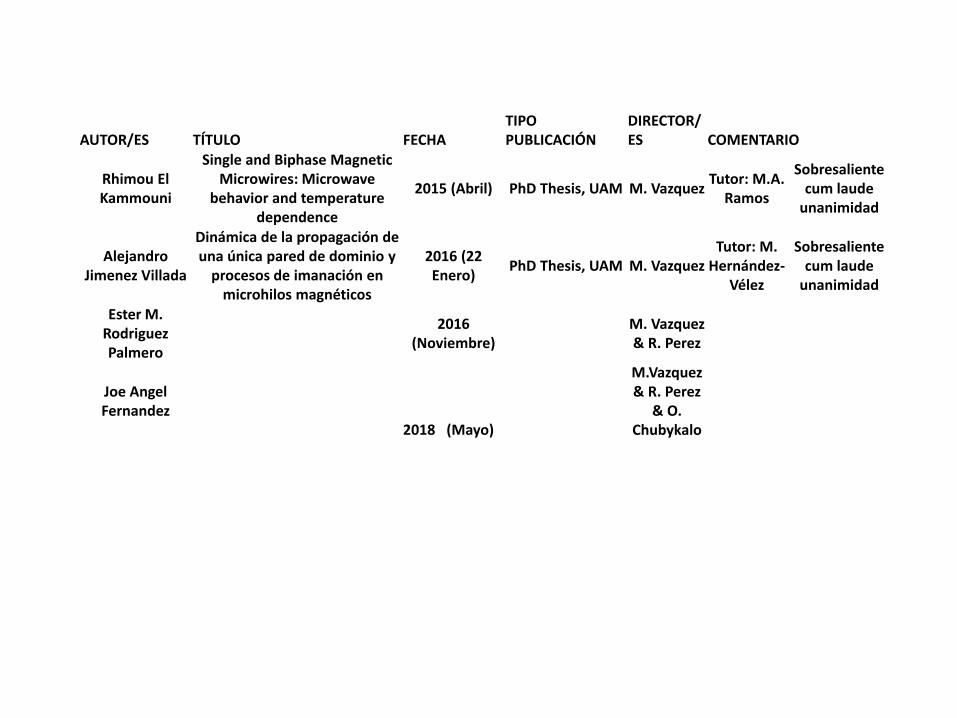
AUTOR/ES TÍTULO FECHA TIPO PUBLICACIÓN
DIRECTOR/ES COMENTARIO
Rhimou El Kammouni
Single and Biphase Magnetic Microwires: Microwave
behavior and temperature dependence
2015 (Abril) PhD Thesis, UAM M. Vazquez Tutor: M.A.
Ramos
Sobresaliente cum laude
unanimidad
Alejandro Jimenez Villada
Dinámica de la propagación de una única pared de dominio y
procesos de imanación en microhilos magnéticos
2016 (22 Enero)
PhD Thesis, UAM M. Vazquez Tutor: M.
Hernández-Vélez
Sobresaliente cum laude
unanimidad
Ester M. Rodriguez Palmero
2016 (Noviembre)
M. Vazquez & R. Perez
Joe Angel Fernandez
2018 (Mayo)
M.Vazquez & R. Perez
& O. Chubykalo
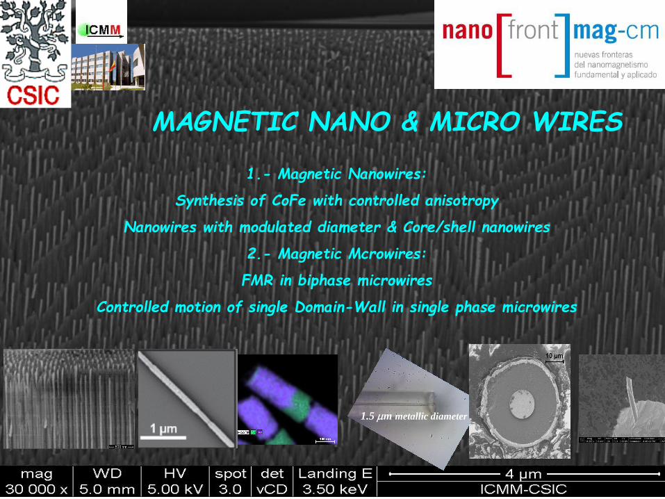
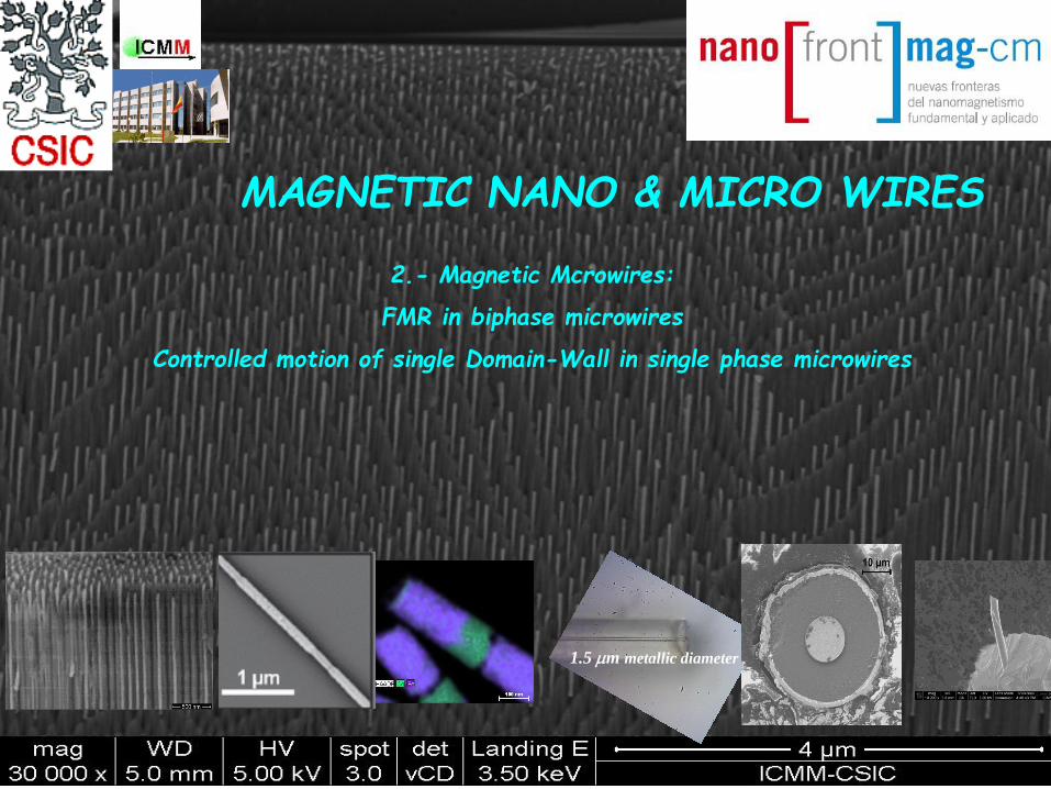
MAGNETIC NANO & MICRO WIRES
1.- Magnetic Nanowires:
Synthesis of CoFe with controlled anisotropy
Nanowires with modulated diameter & Core/shell nanowires
2.- Magnetic Mcrowires:
FMR in biphase microwires
Controlled motion of single Domain-Wall in single phase microwires
1.5 mm metallic diameter

-Looking for specific cylindrical nanowires & arrays - Arrays ar relevant for 3D magnetic architectures, sensor devices, novel magnets, biomagnetic functionalization and beyond - Individual nanowires are nearly ideal systems for fundamental studies on magnetization & reversal - Why Electrochemical route of fabrication? Less-expensive technique Ability to grow various cylindrical nanowires with designed geometry and composition periodical modulations
- Why cylindrical symmetry nanowires? Nanoscale systems profiting of strong shape anisotropy (Diameter: 15nm to 200nm; Length: 100nm to 50mm) Nanocolumns,Nanotubes,Multilayer,Diameter-Modulated, Core@Shell
- Combining magnetic (Co, Fe) elements & alloys to tailor structure and magnetocrystalline anisotropy so magnetic response
Designed Cylindrical Nanowires: Overall Motivation
Self-assembled pore template
CoFe nanowire array
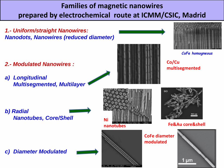
1.- Uniform/straight Nanowires:
Nanodots, Nanowires (reduced diameter)
2.- Modulated Nanowires :
a) Longitudinal
Multisegmented, Multilayer
b) Radial
Nanotubes, Core/Shell
c) Diameter Modulated
Co/Cu multisegmented
Ni nanotubes Fe&Au core&shell
CoFe diameter modulated
Families of magnetic nanowires prepared by electrochemical route at ICMM/CSIC, Madrid
CoFe homogneous
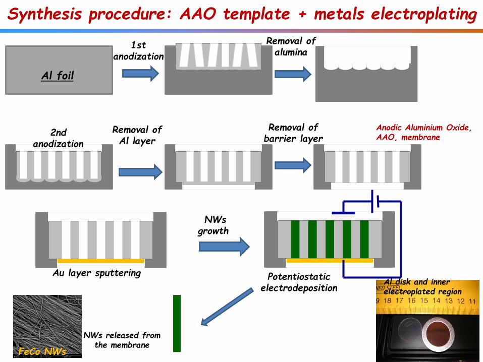
Removal of alumina
Au layer sputtering
NWs growth
Removal of barrier layer
Al foil
Removal of Al layer
1st anodization
2nd anodization
Potentiostatic electrodeposition
Synthesis procedure: AAO template + metals electroplating
Al disk and inner electroplated region
NWs released from the membrane
Anodic Aluminium Oxide, AAO, membrane
FeCo NWs
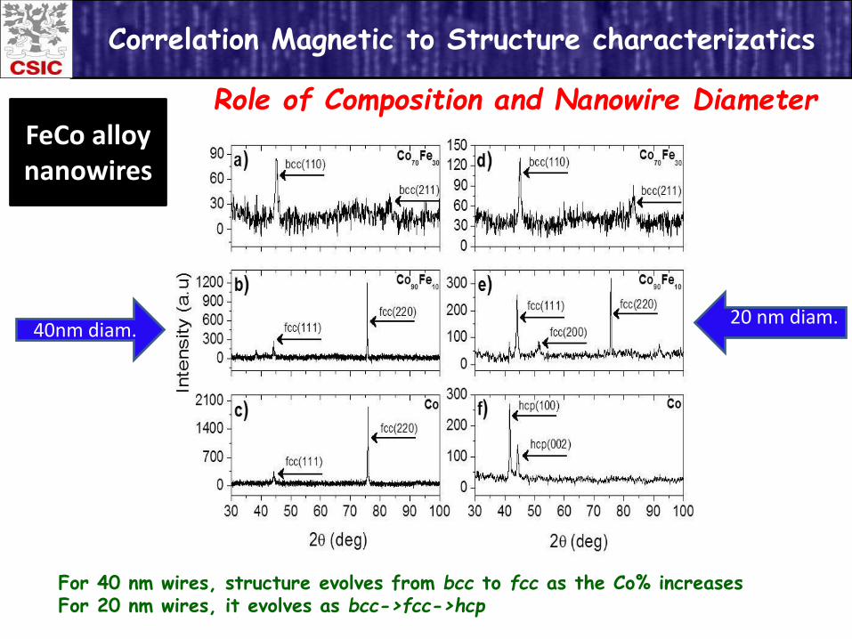
Correlation Magnetic to Structure characterizatics
FeCo alloy nanowires
40nm diam. 20 nm diam.
For 40 nm wires, structure evolves from bcc to fcc as the Co% increases For 20 nm wires, it evolves as bcc->fcc->hcp
Role of Composition and Nanowire Diameter
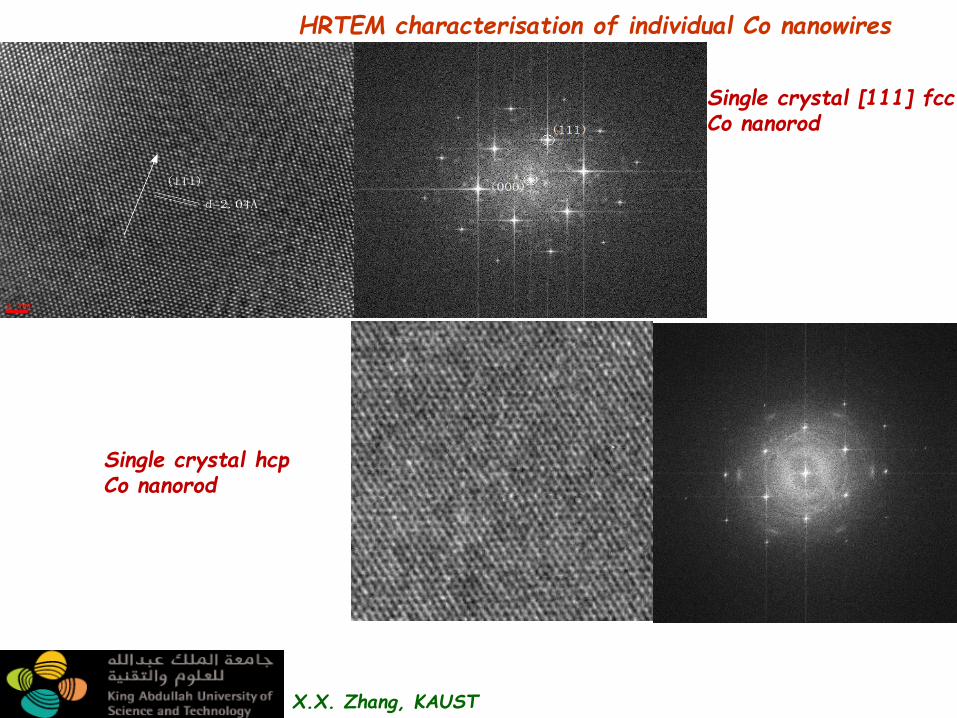
HRTEM characterisation of individual Co nanowires
Single crystal [111] fcc Co nanorod
X.X. Zhang, KAUST
Single crystal hcp Co nanorod

fixed diameter, D=35nm and length, L=3mm
Textured along different directions in hcp-phases with pH of synthesis
Co nanowires: Crystal structure and Magnetic Anisotropy

TEM study of Co nanowires prepared under different electrolyte pH: (a) – pH 3.5, (b) - pH 5.0, (c) – pH 6.0 The insets show the corresponding electron diffraction patterns and HRTEM images The green arrows show the orientation of the c-axis. The white arrows indicate the crystal orientation
Co nanowires: Crystal structure and Magnetic Anisotropy
Yu.P. Ivanov et al. Nanotechnology 2014
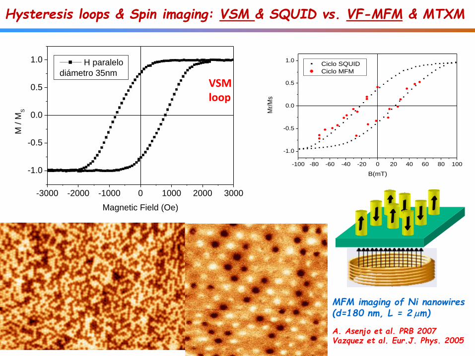
Hysteresis loops & Spin imaging: VSM & SQUID vs. VF-MFM & MTXM
-100 -80 -60 -40 -20 0 20 40 60 80 100
-1.0
-0.5
0.0
0.5
1.0
Mr/
Ms
B(mT)
Ciclo SQUID
Ciclo MFM
MFM imaging of Ni nanowires (d=180 nm, L = 2 mm)
A. Asenjo et al. PRB 2007 Vazquez et al. Eur.J. Phys. 2005
-3000 -2000 -1000 0 1000 2000 3000
-1.0
-0.5
0.0
0.5
1.0
M /
MS
Magnetic Field (Oe)
H paralelo
diámetro 35nm
VSM loop
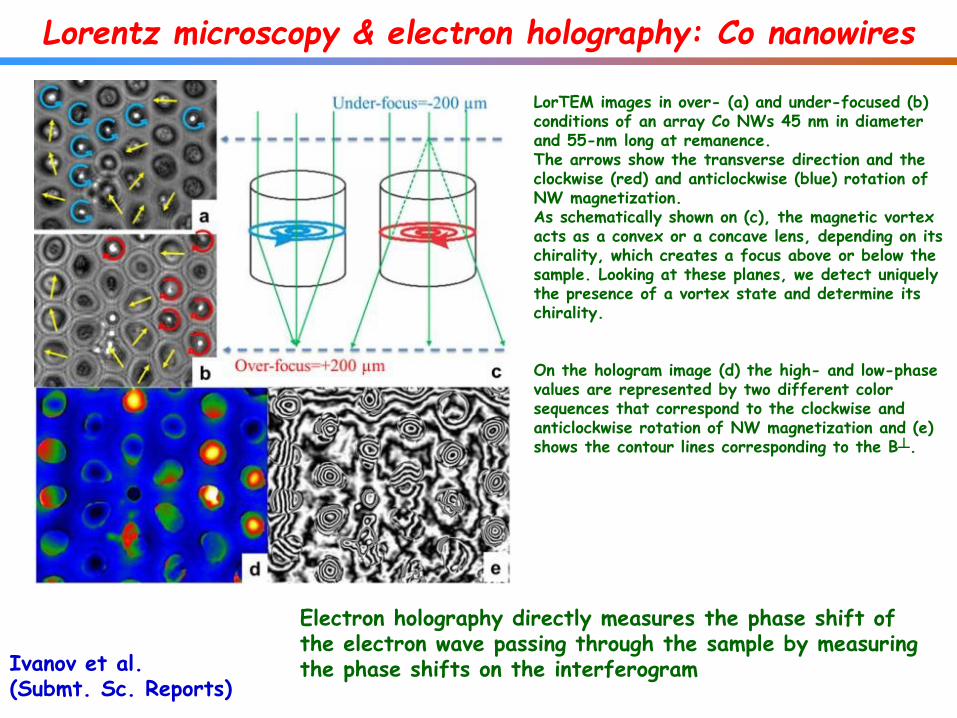
LorTEM images in over- (a) and under-focused (b) conditions of an array Co NWs 45 nm in diameter and 55-nm long at remanence. The arrows show the transverse direction and the clockwise (red) and anticlockwise (blue) rotation of NW magnetization. As schematically shown on (c), the magnetic vortex acts as a convex or a concave lens, depending on its chirality, which creates a focus above or below the sample. Looking at these planes, we detect uniquely the presence of a vortex state and determine its chirality. On the hologram image (d) the high- and low-phase values are represented by two different color sequences that correspond to the clockwise and anticlockwise rotation of NW magnetization and (e) shows the contour lines corresponding to the B┴.
Lorentz microscopy & electron holography: Co nanowires
Electron holography directly measures the phase shift of the electron wave passing through the sample by measuring the phase shifts on the interferogram Ivanov et al.
(Submt. Sc. Reports)

Coercivity Hc as a function of NW diameter for single crystal hcp Co NWs
and different easy axis orientations (defined by the angle θ with NW axis)
Modeling: role of diameter & crystal symmetry
hcp Co nanowires (2 mm long) Changing the reversal mode with Anisotropy easy axis
Regions (1), (2), (3) correspond to applied fields at which a vortex is formed, at the remanence, and when the vortex core is switched
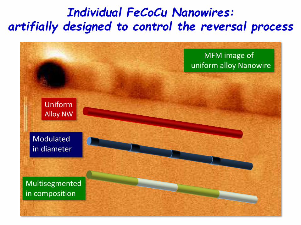
Uniform Alloy NW
Multisegmented in composition
Modulated in diameter
Individual FeCoCu Nanowires: artifially designed to control the reversal process
MFM image of uniform alloy Nanowire
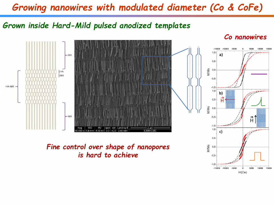
Grown inside Hard-Mild pulsed anodized templates
Growing nanowires with modulated diameter (Co & CoFe)
Co nanowires
Fine control over shape of nanopores is hard to achieve
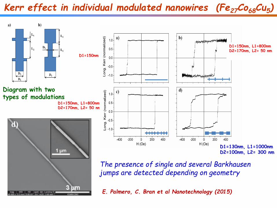
Diagram with two types of modulations
Kerr effect in individual modulated nanowires (Fe27Co68Cu5)
The presence of single and several Barkhausen jumps are detected depending on geometry
E. Palmero, C. Bran et al Nanotechnology (2015)
D1=150nm
D1=150nm, L1=800nm D2=170nm, L2= 50 nm
D1=130nm, L1=1000nm D2=100nm, L2= 300 nm
D1=150nm, L1=800nm D2=170nm, L2= 50 nm
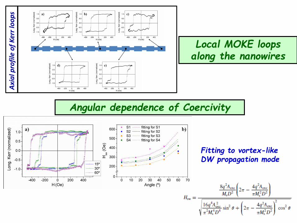
Axi
al p
rofi
le o
f K
err
loo
ps
Angular dependence of Coercivity
Local MOKE loops along the nanowires
Fitting to vortex-like DW propagation mode
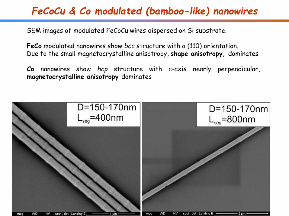
SEM images of modulated FeCoCu wires dispersed on Si substrate. FeCo modulated nanowires show bcc structure with a (110) orientation. Due to the small magnetocrystalline anisotropy, shape anisotropy, dominates Co nanowires show hcp structure with c-axis nearly perpendicular, magnetocrystalline anisotropy dominates
FeCoCu & Co modulated (bamboo-like) nanowires
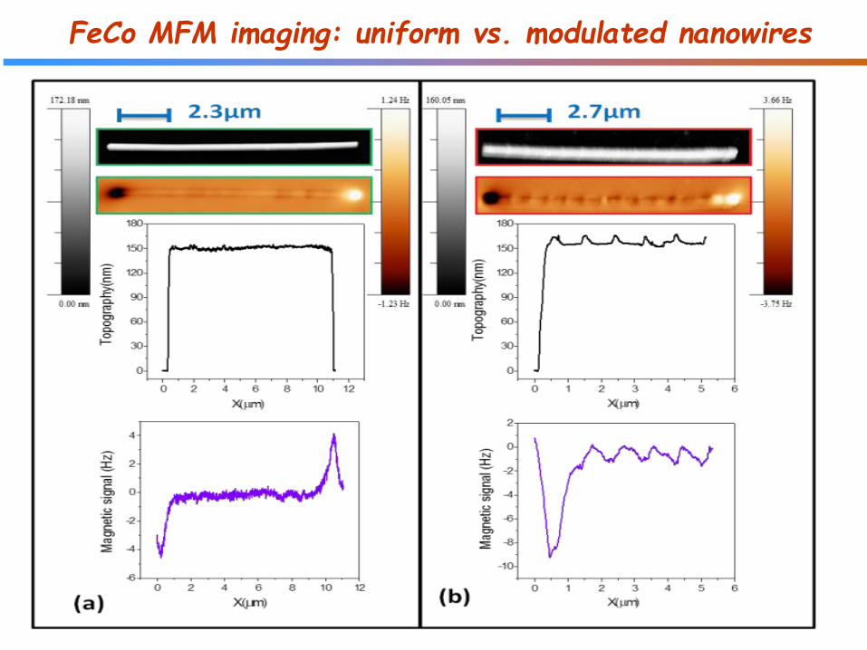
FeCo MFM imaging: uniform vs. modulated nanowires
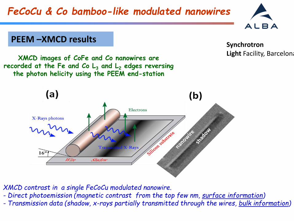
PEEM –XMCD results
XMCD contrast in a single FeCoCu modulated nanowire. - Direct photoemission (magnetic contrast from the top few nm, surface information) - Transmission data (shadow, x-rays partially transmitted through the wires, bulk information)
FeCoCu & Co bamboo-like modulated nanowires
XMCD images of CoFe and Co nanowires are recorded at the Fe and Co L3 and L2 edges reversing
the photon helicity using the PEEM end-station
Synchrotron Light Facility, Barcelona

Co nanowires Axial anisotropy Perpendicular anisotropy
Axial spins at the core
Vortex at the end
FeCoCu nanowires
PEEM –XMCD in bamboo-like modulated nanowires: information on surface and bulk spin configuration
MFM
MFM
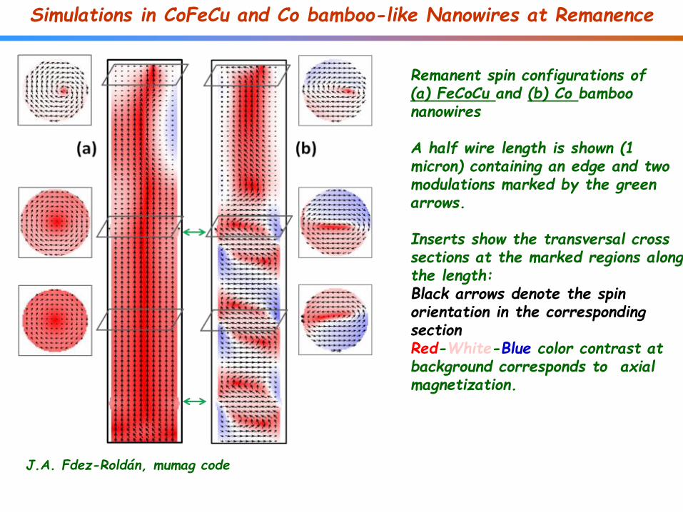
Remanent spin configurations of (a) FeCoCu and (b) Co bamboo nanowires A half wire length is shown (1 micron) containing an edge and two modulations marked by the green arrows. Inserts show the transversal cross sections at the marked regions along the length: Black arrows denote the spin orientation in the corresponding section Red-White-Blue color contrast at background corresponds to axial magnetization.
J.A. Fdez-Roldán, mumag code
Simulations in CoFeCu and Co bamboo-like Nanowires at Remanence
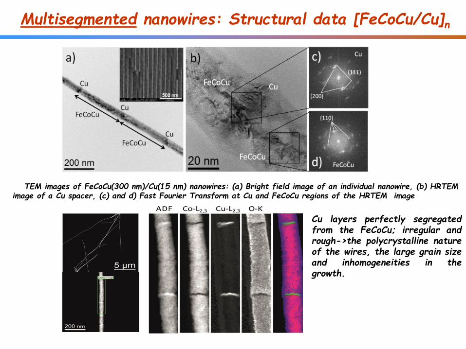
Multisegmented nanowires: Structural data [FeCoCu/Cu]n
TEM images of FeCoCu(300 nm)/Cu(15 nm) nanowires: (a) Bright field image of an individual nanowire, (b) HRTEM image of a Cu spacer, (c) and d) Fast Fourier Transform at Cu and FeCoCu regions of the HRTEM image
Cu layers perfectly segregated from the FeCoCu; irregular and rough->the polycrystalline nature of the wires, the large grain size and inhomogeneities in the growth.
Proenca et al, Phys. Rev. B, 2013
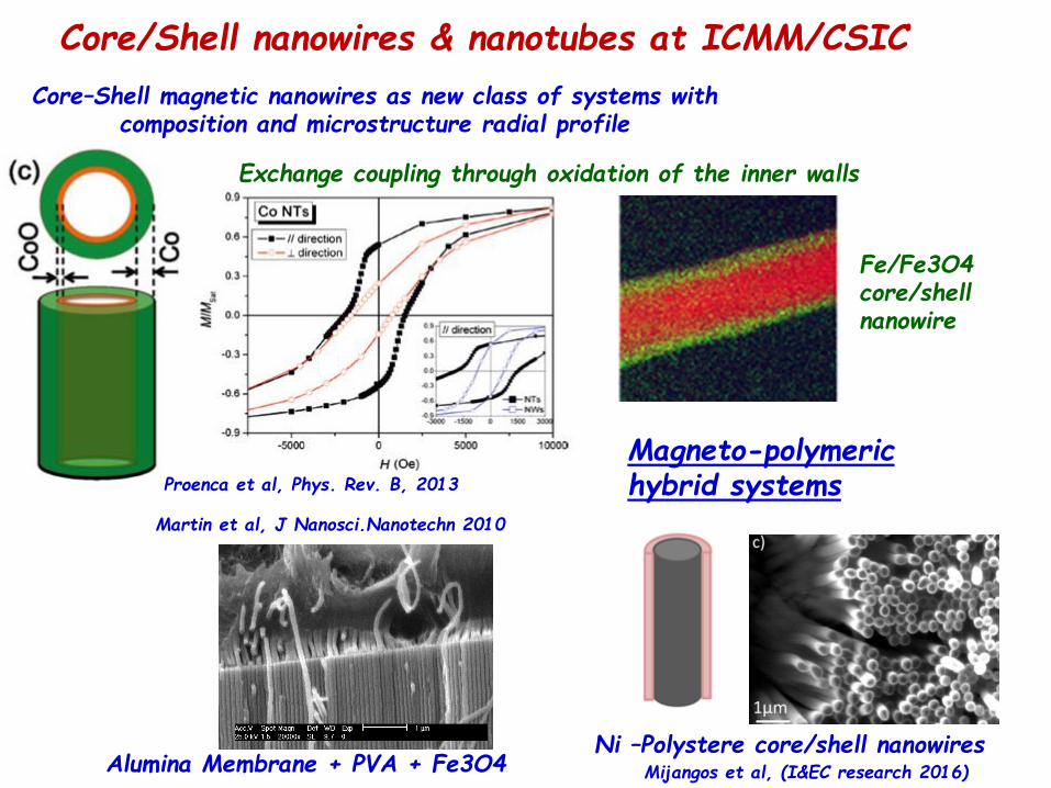
Exchange coupling through oxidation of the inner walls
Core–Shell magnetic nanowires as new class of systems with composition and microstructure radial profile
.
Core/Shell nanowires & nanotubes at ICMM/CSIC
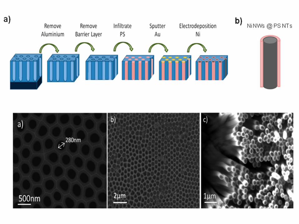
Ni –Polystere core/shell nanowires Alumina Membrane + PVA + Fe3O4 Mijangos et al, (I&EC research 2016)
Martin et al, J Nanosci.Nanotechn 2010
Magneto-polymeric hybrid systems
Fe/Fe3O4 core/shell nanowire
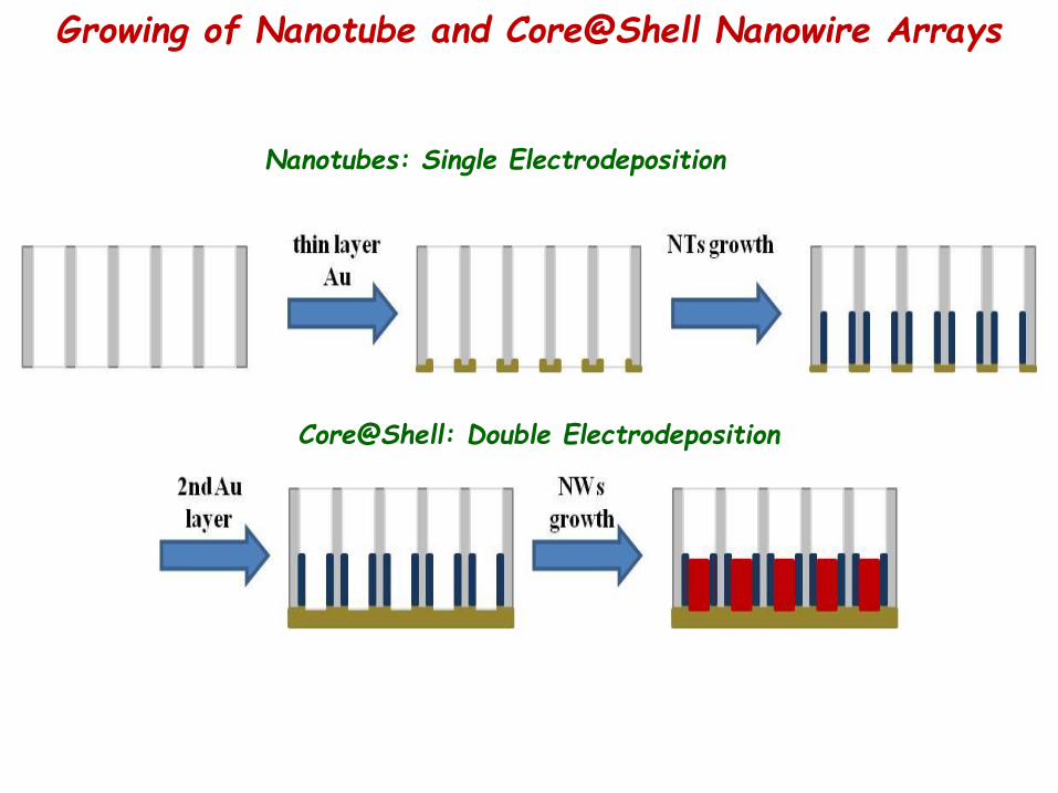
Growing of Nanotube and Core@Shell Nanowire Arrays
Nanotubes: Single Electrodeposition
Core@Shell: Double Electrodeposition
500 nm
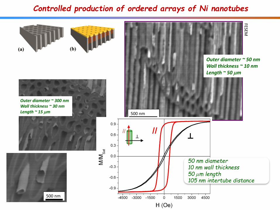
Outer diameter ~ 300 nm Wall thickness ~ 30 nm Length ~ 15 mm 500 nm
FESEM
Controlled production of ordered arrays of Ni nanotubes
Outer diameter ~ 50 nm Wall thickness ~ 10 nm Length ~ 50 mm
50 nm diameter 10 nm wall thickness 50 mm length 105 nm intertube distance
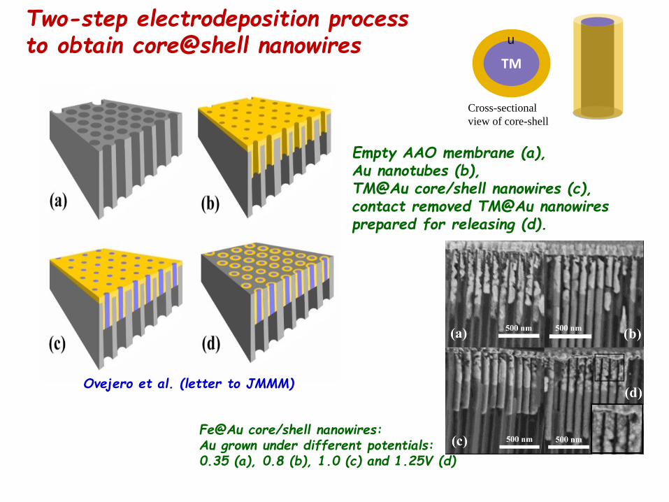
Empty AAO membrane (a), Au nanotubes (b), TM@Au core/shell nanowires (c), contact removed TM@Au nanowires prepared for releasing (d).
Fe@Au core/shell nanowires: Au grown under different potentials: 0.35 (a), 0.8 (b), 1.0 (c) and 1.25V (d)
Two-step electrodeposition process to obtain core@shell nanowires
TM
Au
Cross-sectional
view of core-shell
Ovejero et al. (letter to JMMM)
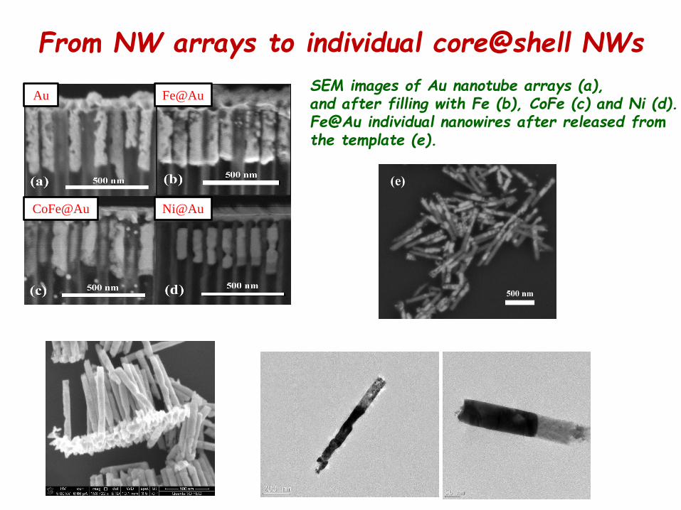
From NW arrays to individual core@shell NWs
SEM images of Au nanotube arrays (a), and after filling with Fe (b), CoFe (c) and Ni (d). Fe@Au individual nanowires after released from the template (e).
Au Fe@Au
CoFe@Au Ni@Au
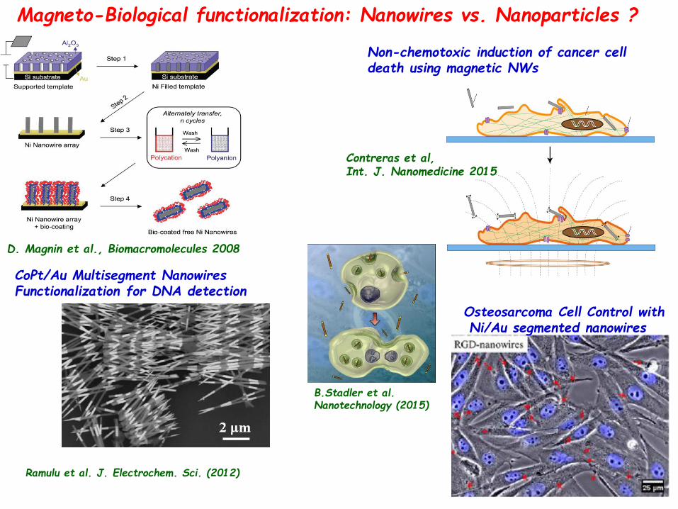
D. Magnin et al., Biomacromolecules 2008
Magneto-Biological functionalization: Nanowires vs. Nanoparticles ?
Non-chemotoxic induction of cancer cell death using magnetic NWs
Contreras et al, Int. J. Nanomedicine 2015
Osteosarcoma Cell Control with Ni/Au segmented nanowires
B.Stadler et al. Nanotechnology (2015)
CoPt/Au Multisegment Nanowires Functionalization for DNA detection
Ramulu et al. J. Electrochem. Sci. (2012)
MAGNETIC NANO & MICRO WIRES
2.- Magnetic Mcrowires:
FMR in biphase microwires
Controlled motion of single Domain-Wall in single phase microwires
1.5 mm metallic diameter
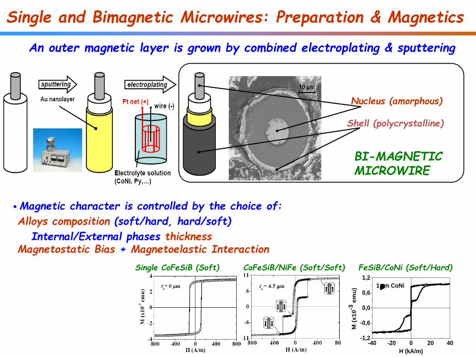
Single and Bimagnetic Microwires: Preparation & Magnetics
An outer magnetic layer is grown by combined electroplating & sputtering
• Magnetic character is controlled by the choice of:
Alloys composition (soft/hard, hard/soft)
Internal/External phases thickness Magnetostatic Bias + Magnetoelastic Interaction
Nucleus (amorphous)
Shell (polycrystalline)
BI-MAGNETIC MICROWIRE
-40 -20 0 20 40-1,2
-0,6
0,0
0,6
1,2
1 mm CoNi
M (
x1
0-3
em
u)
H (kA/m)
Single CoFeSiB (Soft) CoFeSiB/NiFe (Soft/Soft) FeSiB/CoNi (Soft/Hard)
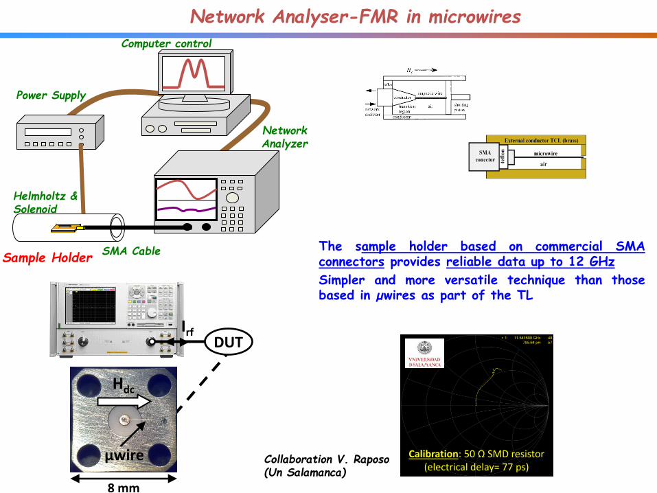
Network Analyser-FMR in microwires
The sample holder based on commercial SMA connectors provides reliable data up to 12 GHz
Simpler and more versatile technique than those based in µwires as part of the TL
DUT Irf
8 mm
Hdc
µwire Calibration: 50 Ω SMD resistor (electrical delay= 77 ps)
Collaboration V. Raposo (Un Salamanca)
Power Supply
Network Analyzer
SMA Cable
Helmholtz & Solenoid
Sample Holder
Computer control
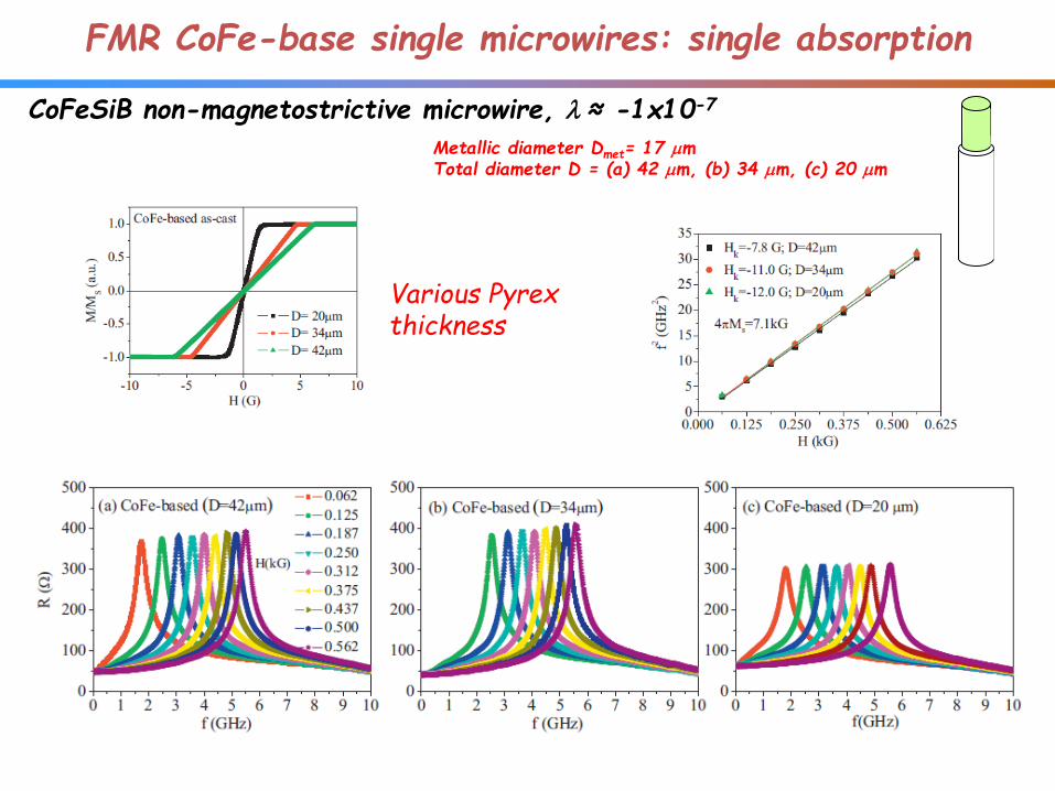
Metallic diameter Dmet= 17 mm Total diameter D = (a) 42 mm, (b) 34 mm, (c) 20 mm
FMR CoFe-base single microwires: single absorption
Various Pyrex thickness
CoFeSiB non-magnetostrictive microwire, l ≈ -1x10⁻⁷

FMR CoFe-base biphase microwires: three absorption peaks
CoFeSiB soft non-magnetostrictive core, l ≈ -1x10⁻⁷
NiFe ultrasoft polycrystalline shell Metallic diameter Dmet= 17 mm Met. + Pyr. diameter D = (a) 42 mm, (b) 34 mm, (c) 20 mm NiFe thickness t= 2 mm
Various Pyrex thickness
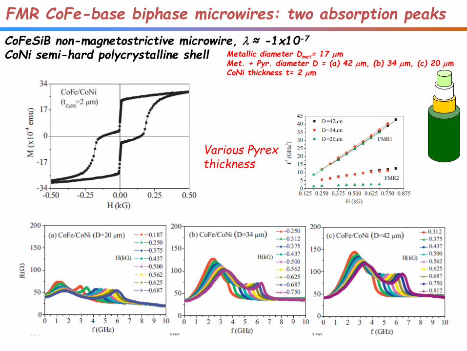
FMR CoFe-base biphase microwires: two absorption peaks
Various Pyrex thickness
CoFeSiB non-magnetostrictive microwire, l ≈ -1x10⁻⁷
CoNi semi-hard polycrystalline shell Metallic diameter Dmet= 17 mm Met. + Pyr. diameter D = (a) 42 mm, (b) 34 mm, (c) 20 mm CoNi thickness t= 2 mm
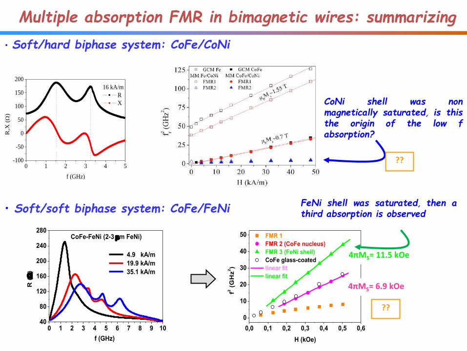
CoNi shell was non magnetically saturated, is this the origin of the low f absorption?
Multiple absorption FMR in bimagnetic wires: summarizing
0 1 2 3 4 5 6 7 8 9 1040
80
120
160
200
240
280
R (
)
f (GHz)
4.9 kA/m
19.9 kA/m
35.1 kA/m
CoFe-FeNi (2-3 mm FeNi)
0,0 0,1 0,2 0,3 0,4 0,5 0,6
0
10
20
30
40
50f2
(G
Hz
2)
H (kOe)
FMR 1
FMR 2 (CoFe nucleus)
FMR 3 (FeNi shell)
CoFe glass-coated
linear fit
linear fit
4πMS= 11.5 kOe
4πMS= 6.9 kOe
??
• Soft/soft biphase system: CoFe/FeNi
• Soft/hard biphase system: CoFe/CoNi
FeNi shell was saturated, then a third absorption is observed
0 1 2 3 4 5-100
-50
0
50
100
150
200
R,X
(
)
f (GHz)
16 kA/m
R
X
??

Scheme of nucleation & depinning & propagation of a single Domain Wall (Magnetostrictive Fe rich microwires)
+ + - - - + +
+ +
+ + + - -
- -
- - + +
+ - - - -
- -
-
- +
-
- +
- -
+
+ + -
- -
+
+
+
-400 -200 0 200 400
-0,8
-0,4
0,0
0,4
0,8
M (
em
u)x
10
H (A/m)
Hsw ~ (1/m0MsVcr) { aEg+ bEsf}
DW
Reversal spontaneously begins at one end of the wire at a critical switching field
1.5 mm metallic diameter
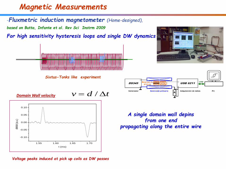
-Fluxmetric induction magnetometer (Home-designed),
based on Butta, Infante et al. Rev Sci Instrm 2009
For high sensitivity hysteresis loops and single DW dynamics
Magnetic Measurements
Voltage peaks induced at pick up coils as DW passes
t
Domain Wall velocity
Sixtus-Tonks like experiment
A single domain wall depins from one end
propagating along the entire wire
tdv /
1.55 1.60 1.65 1.70
-0.10
-0.05
0.00
0.05
0.10
dM/d
t (a.
u.)
t (ms)
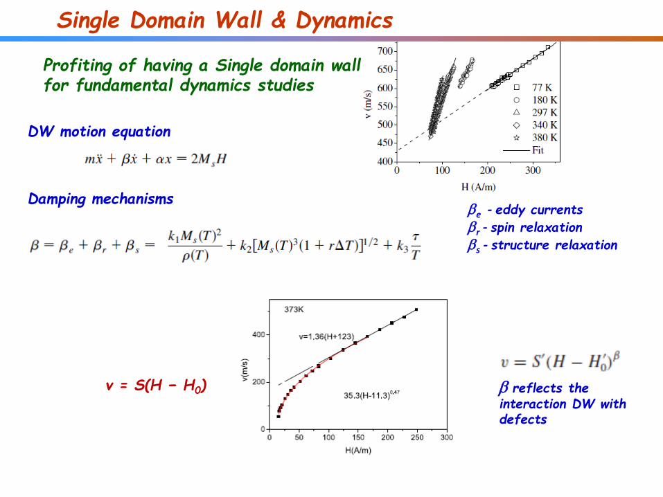
v = S(H − H0)
be - eddy currents br - spin relaxation bs - structure relaxation
b reflects the interaction DW with defects
Single Domain Wall & Dynamics
Profiting of having a Single domain wall for fundamental dynamics studies
Damping mechanisms
DW motion equation

Exp. 1.-Trapping a Domain Wall: Sixtus & Tonks–like
- Homogeneous drive field, Hdr (solenoid) - Local field, HL - Two symmetric pick-up coils - Asymmetric positioning of the microwire: essential for the depinning of the standard wall, DWst, at the left wire’s end and its rigthward propagation
Under applied drive field by the solenoid, a reverse domain nucleates at the left wire’s end, and a “standard” wall depins and propagates along the wire
FeSiB microwire, 10 mm metallic diameter
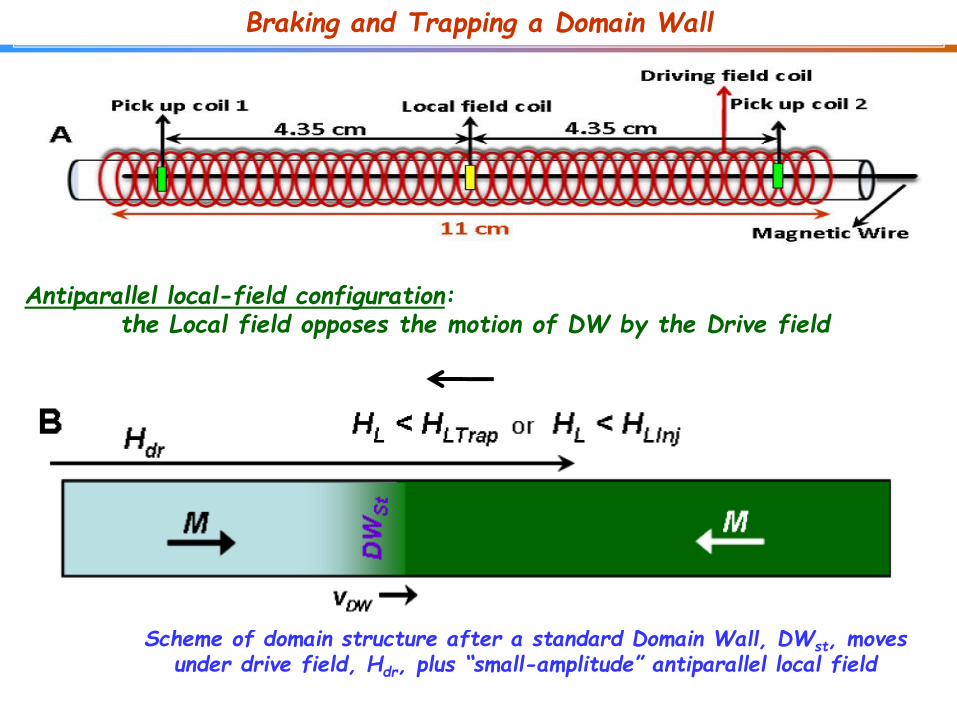
Scheme of domain structure after a standard Domain Wall, DWst, moves under drive field, Hdr, plus “small-amplitude” antiparallel local field
Antiparallel local-field configuration: the Local field opposes the motion of DW by the Drive field
Braking and Trapping a Domain Wall
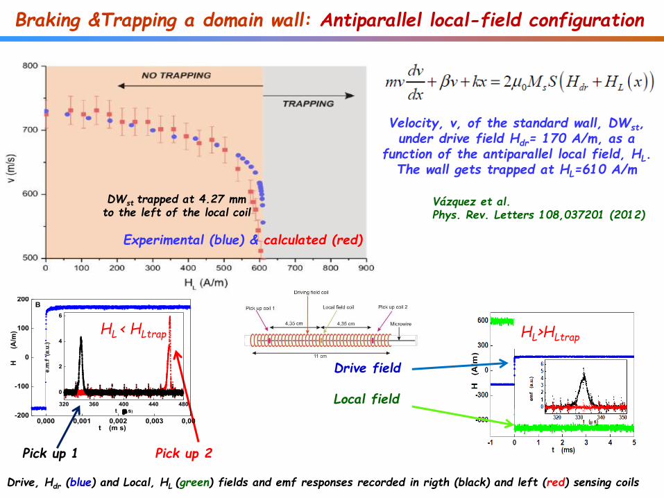
Braking &Trapping a domain wall: Antiparallel local-field configuration
DWst trapped at 4.27 mm to the left of the local coil
Experimental (blue) & calculated (red)
Pick up 1 Pick up 2
0,000 0,001 0,002 0,003 0,004-200
-100
0
100
200
320 360 400 440 480
0
2
4
6
H
(A/m
)
t (m s)
B
t (m s)
e.m
.f
(a.u
.)
Drive field Local field
HL>HLtrap
Drive, Hdr (blue) and Local, HL (green) fields and emf responses recorded in rigth (black) and left (red) sensing coils
HL < HLtrap
Velocity, v, of the standard wall, DWst, under drive field Hdr= 170 A/m, as a
function of the antiparallel local field, HL. The wall gets trapped at HL=610 A/m
Vázquez et al. Phys. Rev. Letters 108,037201 (2012)

Exp. 2.-Playing with the propagation of Single DW
The sequence of colored peaks confirms a Rightwards motion of the Single DW
for rightwards (bottom) and leftwards (upper)
applied field
Fe79Si10B8C3 microwire (dmet=20.5 mm, Dtot=30.5 mm)
- Multiple-coil system (2000 turns, 2 mm wide) - Extended length: 40 cm long wires - Square shaped 40 Hz field
A. Jimenez et al., Eur Phys J B 86, 113 (2013) invited JEMS 2012
microwire
S1 yellow
S2 blue
S3 pink
S4 green Pick-up coils Si
“Small” Applied Field, H = ± 213 A/m
H
H

“Medium” Applied Field = ± 262 A/m
H
S4 S3 S2 S1
DWst1 v
S4 S3 S2 S1
0H
S4 S3 S2 S1
DWst2
v
H
v
DWrev
Single DW rightwards motion (bottom) Two DWs moving in opposite directions (upper)
microwire
S1 yellow
S2 blue
S3 pink
S4 green
For Happ=-262 A/m, the signal at S4 (green) is received before the one in S3 (pink) denoting the presence of a second reverse wall, DWrev, propagating in the opposite direction
H
H
The appearance of a second DW moving opposite
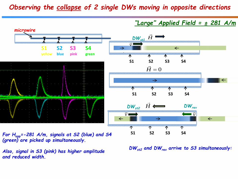
“Large” Applied Field = ± 281 A/m
H
S4 S3 S2 S1
DWst1 v
S4 S3 S2 S1
0H
S4 S3 S2 S1
DWst2
v
H
v
DWrev
DWst2 and DWrev arrive to S3 simultaneously:
microwire
S1 yellow
S2 blue
S3 pink
S4 green
For Happ=-281 A/m, signals at S2 (blue) and S4 (green) are picked up simultaneously. Also, signal in S3 (pink) has higher amplitude and reduced width.
Observing the collapse of 2 single DWs moving in opposite directions

www.icmm.csic.es/gnmp/
Inst. Materials Science of Madrid
David Trabada Rafael P. del Real
Jose Miguel García Cristina Bran
Laura Vivas Rhimou ElKammouni
Ester Palmero
Oksana Chubykalo Yurii Ivanov Agustina Asenjo
Group of Nanomagnetism and Magnetization Processes
the scientific team in winter excursion by the mountains in Segovia looking for the roasted lamb Patones de Arriba,
Dec. 2015