
경종민 [email protected] 1 Future Prospect of IC Technology (ITRS) 2002. 9.9.
56
-
Upload
kerry-johnson -
Category
Documents
-
view
218 -
download
4
Transcript of 경종민 [email protected] 1 Future Prospect of IC Technology (ITRS) 2002. 9.9.
2
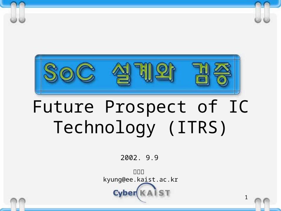
Contents• Introduction
– ITRS
• Overall Roadmap– Product Generation– Lithography– Package– Power– Cost
• Design Technology Challenges– Introduction– Complexity, Methodology– Design Technology Challenges
3
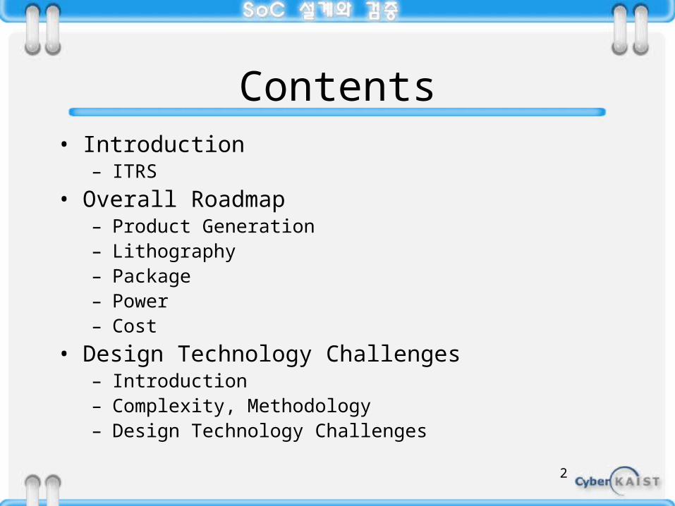
ITRS Introduction• ITRS
International Technology Roadmap for Semiconductors
– Predicts the main trends in the semiconductor industry– Provides a reference of requirements, potential solutions, an
d their timing for the semiconductor industry– ITWG (International Technology Working Group)http://public.itrs.net
1992NTRS 1994
NTRS 1997NTRS
1998Update
1999ITRS
2000update
2001ITRS
SIA
4
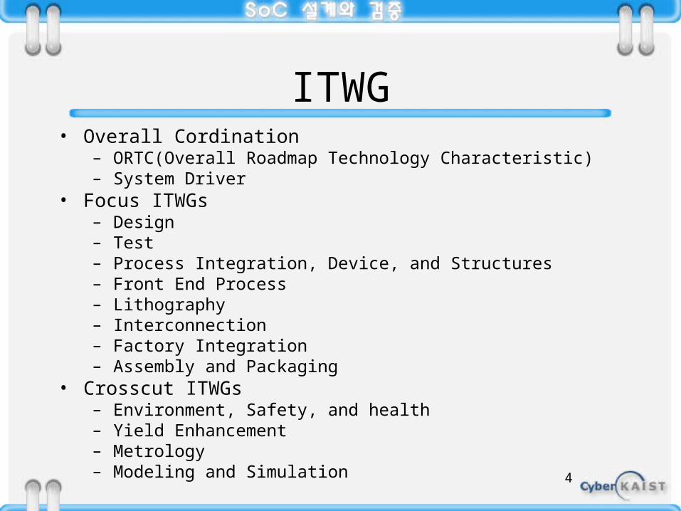
ITWG• Overall Cordination
– ORTC(Overall Roadmap Technology Characteristic)– System Driver
• Focus ITWGs– Design– Test– Process Integration, Device, and Structures– Front End Process– Lithography– Interconnection– Factory Integration– Assembly and Packaging
• Crosscut ITWGs– Environment, Safety, and health– Yield Enhancement– Metrology– Modeling and Simulation
5
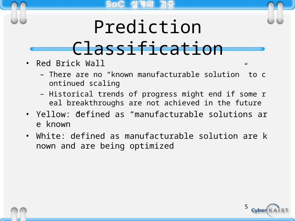
Prediction Classification• Red Brick Wall
– There are no “known manufacturable solution” to continued scaling– Historical trends of progress might end if some real breakthroughs a
re not achieved in the future• Yellow: defined as “manufacturable solutions are known”• White: defined as manufacturable solution are known and are be
ing optimized
6
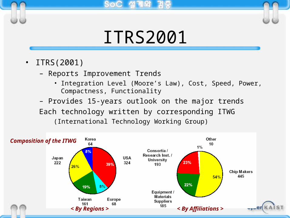
ITRS2001• ITRS(2001)
– Reports Improvement Trends• Integration Level (Moore’s Law), Cost, Speed, Power,
Compactness, Functionality
– Provides 15-years outlook on the major trendsEach technology written by corresponding ITWG
(International Technology Working Group)
Composition of the ITWG
< By Regions >
< By Affiliations >
7
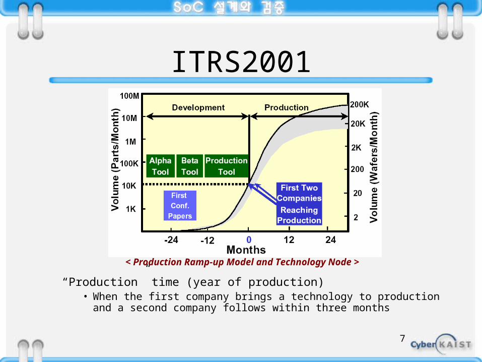
ITRS2001
“Production” time (year of production)• When the first company brings a technology to production
and a second company follows within three months
< Production Ramp-up Model and Technology Node >
8
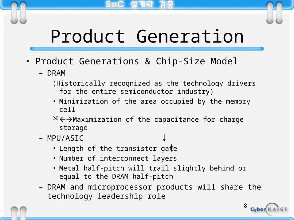
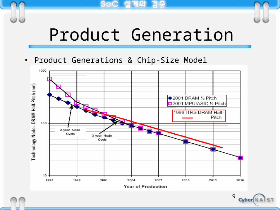
Product Generation• Product Generations & Chip-Size Model
– DRAM(Historically recognized as the technology drivers for the
entire semiconductor industry)• Minimization of the area occupied by the memory cellMaximization of the capacitance for charge storage
– MPU/ASIC• Length of the transistor gate• Number of interconnect layers• Metal half-pitch will trail slightly behind or equal to the
DRAM half-pitch
– DRAM and microprocessor products will share the technology leadership role
9
Product Generation• Product Generations & Chip-Size Model
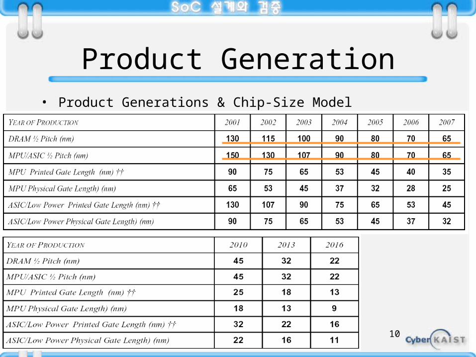
10
Product Generation• Product Generations & Chip-Size Model
11
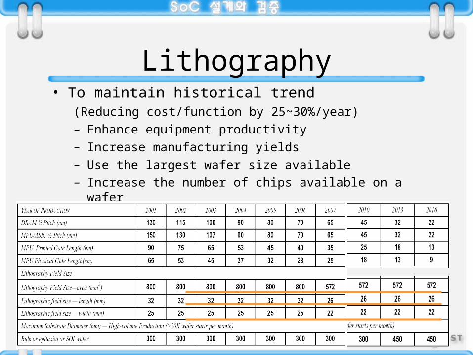
Lithography• To maintain historical trend
(Reducing cost/function by 25~30%/year)– Enhance equipment productivity– Increase manufacturing yields– Use the largest wafer size available– Increase the number of chips available on a wafer
12
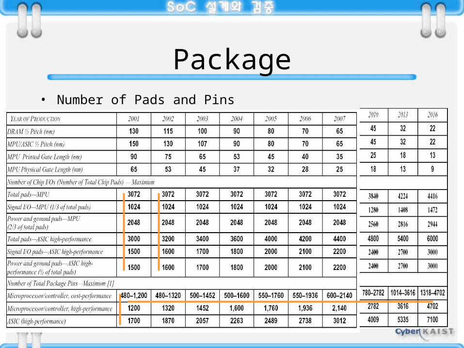
Package• Number of Pads and Pins
– Increase number of I/O signals• For higher number of functions on a single chip
– Additional power and ground connectionsTo optimize power managementTo increase noise immunity• MPU (1:2 = I/O : power/ground)
– Two power/ground pads for every signal I/O pad
• ASIC (1:1)– One power/ground pad for every signal I/O pad
13
Package• Number of Pads and Pins
14
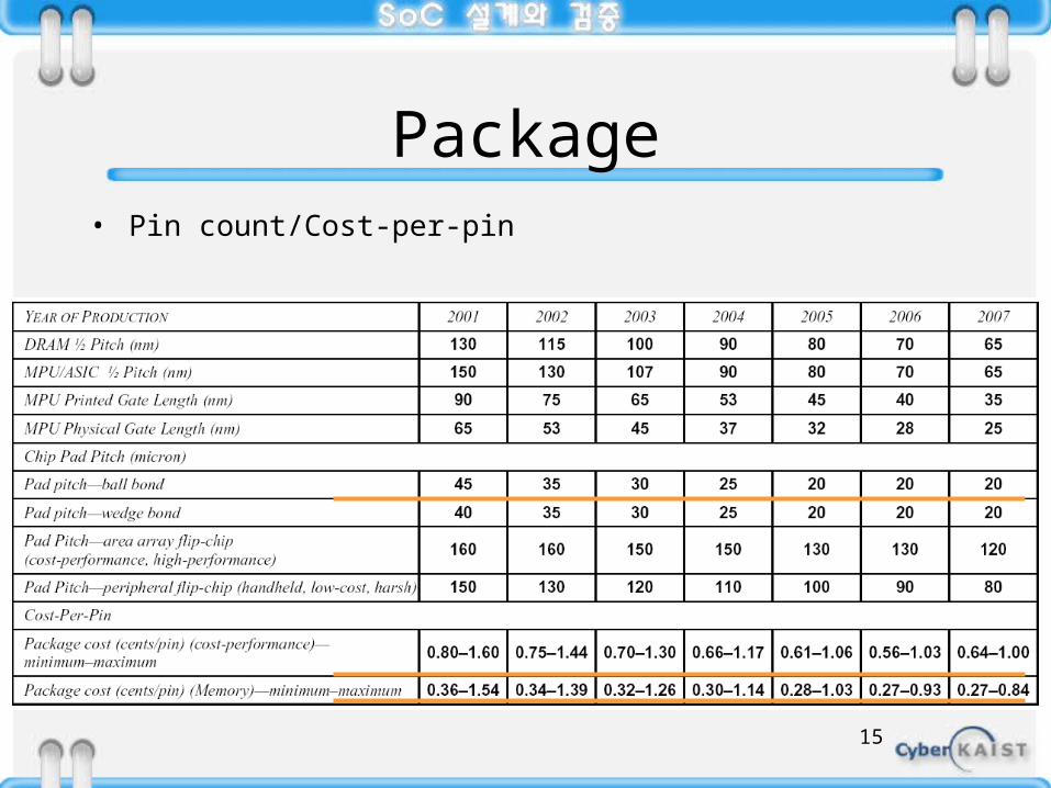
Package• Pin count/Cost-per-pin
# of package pin/balls increases at 10%/yearCost/pin decreases at 5%/year Average cost of packaging will increase at 5%/years– To reduce the overall system pin requirements
• Combining functionality into SOC• Multi-chip modules• Bumped chip-on-board
15
Package• Pin count/Cost-per-pin
16
Package• Electrical Signals
Instructions/second doubles every 1.5~2 yearsIncrease Processing power– To optimize signal and power distribution
• Increasing # of layers of interconnect• Size downscaling of interconnect • Using copper(low resistivity)• Using inter-metal insulating materials of lower dielectric constant
17
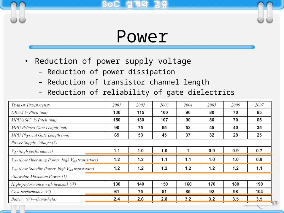
Power• Reduction of power supply voltage
– Reduction of power dissipation– Reduction of transistor channel length– Reduction of reliability of gate dielectrics
18
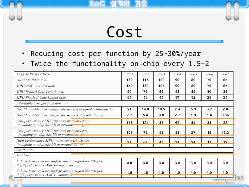
Cost• Reducing cost per function by 25~30%/year• Twice the functionality on-chip every 1.5~2 years
19
DT Introduction• DT
– Enables the conception, implementation, and validation of microelectronics-based systems.
– Include tools, libraries, manufacturing process characterization, and methodologies
• Area– Design Process– System-Level Design– Logical/Circuit/Physical Design– Design Verification– Design Test
• Crosscutting Challenges– Productivity– Power– Manufacturing Integration– Interference – Error-Tolerance
20
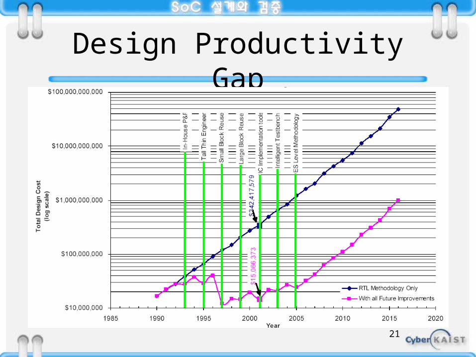
Design Productivity Gap# of available transistors grows faster than the ability to
design them meaningfullyInvestment in process technology has by far dominated
investment in design technology
– Software now routinely accounts for 80% of embedded systems development cost
– Verification engineers are twice as numerous as design engineers on microprocessor project team
– Test cost has grown exponentially relative to manufacturing cost
21
Design Productivity Gap
22
DT Complexity• Silicon Complexity
1. Non-ideal scaling of device parasitics and supply/threshold voltages • Leakage, power management, circuit/device innovation, current delivery
2. Coupled high-frequency device and interconnect• Noise/interference, signal integrity analysis and management, substrate coupling, delay variation due to cross-c
oupling
3. Manufacturing equipment• Statistical process modeling, library characterization
4. Scaling of global interconnect performance relative to device performance• Communication, synchronization
5. Decreased reliability• Gate insulator tunneling and breakdown integrity, joule heating and electromigration, single-event upset, general
fault-tolerance
6. Complexity of manufacturing handoff• Reticle enhancement and mask writing/inspection flow, NRE cost
7. Process variability• Library characterization, analog and digital circuit performance, error-tolerant design, layout, reuse, reliable and
predictable implementation platforms
23
DT Complexity• System Complexity
1. Reuse• Support for hierarchical design, heterogeneous SOC integration (modeling, simulation, verification,
test of component blocks) especially for analog/mixed-signal
2. Verification and test• Specification capture, design for verifiability, verification reuse for heterogeneous SOC, system-level
and software verification, verification of analog/mixed-signal and novel devices, self-test, intelligent noise/delay fault testing, tester timing limits, test reuse
3. Cost-driven design optimization• Manufacturing cost modeling and analysis, quality metrics, co-optimization at die-package-system
levels, optimization with respect to multiple system objectives such as fault tolerance, testability, etc.
4. Embedded software design• Predictable platform-based system design methodologies, co-design with hardware and for
networked system environments, software verification/analysis
5. Reliable implementation platform• Predictable chip implementation into multiple circuit fabrics, higher-level handoff to implementation
6. Design process management• Design team size and geographic distribution, data management, collaborative design support,
“design through system” supply chain management, metrics and continuous process improvement
24
DT Methodology Precepts• Design Methodology combines
– Top-down planning and search (system specification and constraints) with
– Bottom-up propagation (physical laws, limits of manufacturing technology/cost)
25
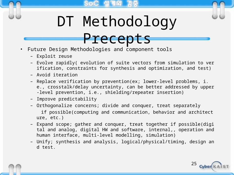
DT Methodology Precepts• Future Design Methodologies and component tools
– Exploit reuse– Evolve rapidly( evolution of suite vectors from simulation to verification, cons
traints for synthesis and optimization, and test)– Avoid iteration– Replace verification by prevention(ex; lower-level problems, i.e., crosstalk/de
lay uncertainty, can be better addressed by upper-level prevention, i.e., shielding/repeater insertion)
– Improve predictability– Orthogonalize concerns; divide and conquer, treat separately if possible(computing and communication, behavior and architecture, etc.)– Expand scope; gather and conquer, treat together if possible(digital and anal
og, digital HW and software, internal,, operation and human interface, multi-level modelling, simulation)
– Unify; synthesis and analysis, logical/physical/timing, design and test.
26
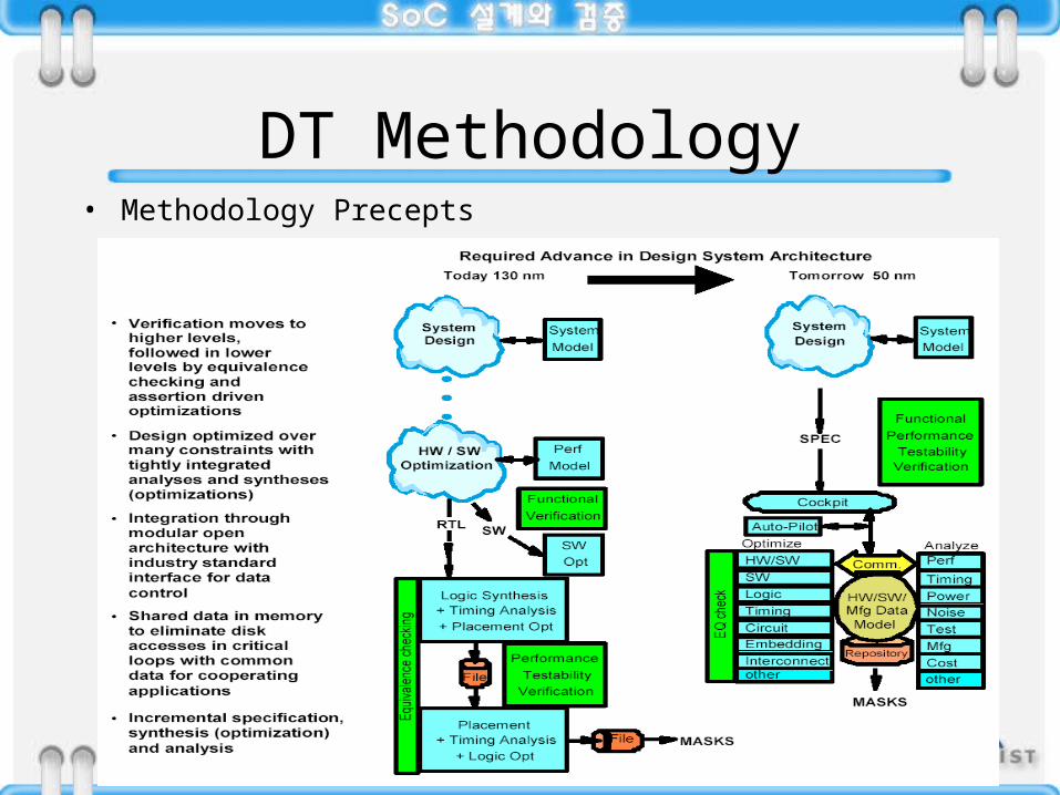
DT Methodology• Methodology Precepts
27
Design Technology• DT Area
– Design Process– System-Level Design– Logical, Circuit, and Physical Design– Design Verification– Design Test
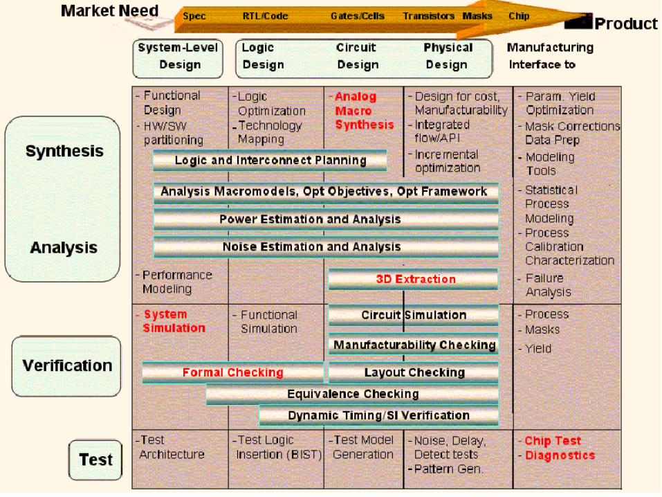
28
Design Technology
29
Design Process Challenges[ ≥65nm / Through 2007 ]1. Design Sharing and Reuse
– Geographically distributed and multi-company design projects
– Integration of multi-vendor and internal design technology (MPU, SOC)
– Standard information model for IC design data, with standard interface (access mechanism) adopted across tools, database (MPU, SOC)
– Tool interoperability that minimized data translation time and redundancy to reduce design cycle times (MPU, SOC)
– Reduction of integration cost
30
Design Process Challenges2. Increased System and Silicon Complexities
– Device count, scaling, operating frequency, power and noise management (MPU, SOC)
– Incremental analysis and optimization capability for constraint-dominated design, with runtimes proportional to amount of design changed (MPU, SOC)
– Scalable design optimization algorithms– Concurrent execution of design and analysis tools with
appropriate objectives and abstractions (MPU, SOC)– Common device, wafer recipe and equipment
characterizations, controlled by process owner and packaged for “immutable interpretation” by design and analysis tools
31
Design Process Challenges3. Time-to-market for cost-driven SOC
– Common information models to support reuse and (cost-driven) design space exploration (SOC)
– Design rules and information models (e.g., abstracts) that assure reusability; design and validation tools to assure these rules for reusable design IP (SOC)
– DT integration for hardware/software, digital/analog, MEMS, memory, design tools (AMS, SOC)
– Synthesis of analog designs comparable to digital RTL-based synthesis (AMS, SOC)
4. Systematic improvement of design process and design productivity– Standard design process metrics, calibration and
benchmarking
32
Design Process Challenges[ ≤65nm / Beyond 2007 ]1. Time-to-market for cost-driven SOC
– Platform- and application- (and even design-) specific design flows via reusable, interoperable tools (SOC)
– Synthesis of mixed-technology design (including analog) comparable to digital RTL-base synthesis (AMS, SOC)
– System cost minimization tools spanning from standardized process description to supply chain management (SOC)
– Higher-level verification of function, performance and manufacturability (SOC, MPU)
33
Design Process Challenges2. Systematic improvement of design process
and design productivity– Design technology productivity analysis and
optimization tools– Predictable physical implementation flows, along
with predictive models for such flows
34
DT Crosscutting Challenges
• Productivity• Power• Manufacturing Integration• Interference• Error-Tolerance
35
System-Level Design• System-Level Design
– Enable to allocate and exploit silicon resources in a top-down and structured fashion
– Design freedom either behavior for system function, or architecture for system platform with two architecture components, (HW,SW).
– SL DT has both methodological aspect (space exploration and model refinement) and design automation aspect(tools and algorithms)
– Rely on extensive reuse of predesigned IP blocks and functions– Major SL DT trends: 1)reuse and platform-based design 2)increasingly prohibitive cost of communication/synchronization 3)heterogeneous integration 4)embedded software
36
SL Design Challenges[ ≥65nm / Through 2007 ]1. System Complexity
– Higher-level abstraction and specification• Design language infrastructure for complex models• C++ derivatives such as SystemC and others
– Dynamism and softness• Enable the system to adapt at runtime under the influence of use requireme
nts• Enables a system to be modified or reprogrammed• New abstractions are required for such runtime modification of function and
architecture– System-level reuse
• Already some progress in RT- and Layout-level design reuse• No methodology and associated design tool• Reuse of complex HW-SW architectures via methods
– Such as platform-based design
37
SL Design Challenges1. System Complexity (continued)
– Design space exploration and system-level estimation• For optimization of the function-architecture mapping
– Power, area throughput, etc
– Efficient behavioral synthesis and SW compilation• Automated mappings from function to architecture
– Behavioral synthesis for hardware and compilation of software
– Automatic interface synthesis• Synthesizing Interfaces (between HW-HW, HW-SW, SW-SW) • Instead of hand-designed or drawn from parameterized
libraries
38
SL Design Challenges2. System Power Consumption
– Energy-performance-flexibility tradeoffs– Novel data transfer and storage techniques
3. Integration of heterogeneous technologies– Codesign
Partitioning and codesign• HW-SW, analog-digital, fixed-reprogrammable, die-package-board
– Analog behavioral modeling and synthesis: Non-scalability• Automated analog circuit synthesis and optimization• Language-level modeling methodologies
– Top-down implementation planning with diverse fabrics• Single hierarchical mixed-technology planning environment
39
SL Design Challenges4. Embedded Software
– SW-SW codesign into highly programmable platform– System capture and abstraction
• System functional model, communication model– New automation from high level description to HW-SW implementat
ions, include SW synthesis– HW-SW coverification
5. Links to verification, test and cultureShifting design focus from block creation to block reuse– Integration-oriented verification and test architecture– Divergent design practices and culture
• Supporting connection point, links between system-level design and implementation
– Between ever-greater abstractions and detailed physical manufacturing realities
40
SL Design Challenges[ ≤65nm / Beyond 2007 ]1. System Complexity
– Communication-centric design and network-based communication on chip
– Design robustness
2. System Power Consumption– Non-scaling of centrally organized architectures– Building large systems from heterogeneous SOCs
3. Integration of heterogeneous technologies– Total system integration including new integrated technologies (e.
g., MEMS, electro-optical, electro-chemical, electro-biological or organic)
41
Logical, circuit, Physical Design
[ ≥65nm / Through 2007 ]1. Efficient and Predictable Implementation
– Scalable, incremental analyses and optimization– Unified implementation/interconnect planning and estimation/predictio
n– Synchronization and global signaling– Heterogeneous system composition– Links to verification and test
2. Variability and design-manufacturing interface– Uncertainty of fundamental chip parameters (timing, skew, matching) d
ue to manufacturing and dynamic variability sources (MPU, SOC, AMS)– Process modeling and characterization– Cost-effective circuit, layout and reticle enhancement to manage manu
facturing variability
42
Logical, circuit, Physical Design
3. Silicon complexity, non-ideal device scaling and power management– Leakage and power management– Reliability and fault tolerance– Analysis complexity and consistent analysis / synthesis
objective
4. Circuit design to fully exploit device technology innovation– Support for new circuit families that address power and
performance challenges– Implementation tools for SOI– Analog synthesis
43
Logical, circuit, Physical Design
[ ≤65nm / Beyond 2007 ]1. Efficient and Predictable Implementation
– Reliable, predictable fabric- and application-specification implementation platforms
– Cost-driven implementation flows2. Variability and design-manufacturing interface
– Increasing atomic-scale variability effects3. Silicon complexity, non-ideal device scaling and power
management– Recapture of reliability lost in manufacturing test
4. Circuit design to fully exploit device technology innovation– Increasing atomic-scale effects– Adaptive and self-repairing circuits– Low-power sensing and sensor interface circuits; micro-
optical devices
44
Design Verification• Major role to the design process
– The dominant cost in the design process– Verification engineers outnumber designers (2~3times) in the
most complex designs• Why
– Increasing functional complexity– Other aspects of the design process has produced enormous
progress, leaving verification as the bottleneck• Current Verification Method
– Trial-and-error verification method• Verify the functionality by repeatedly building models• Simulating them on ad hoc selection of vectors
– Slow and unscalable• Doubly-exponential growth in functional complexity
45
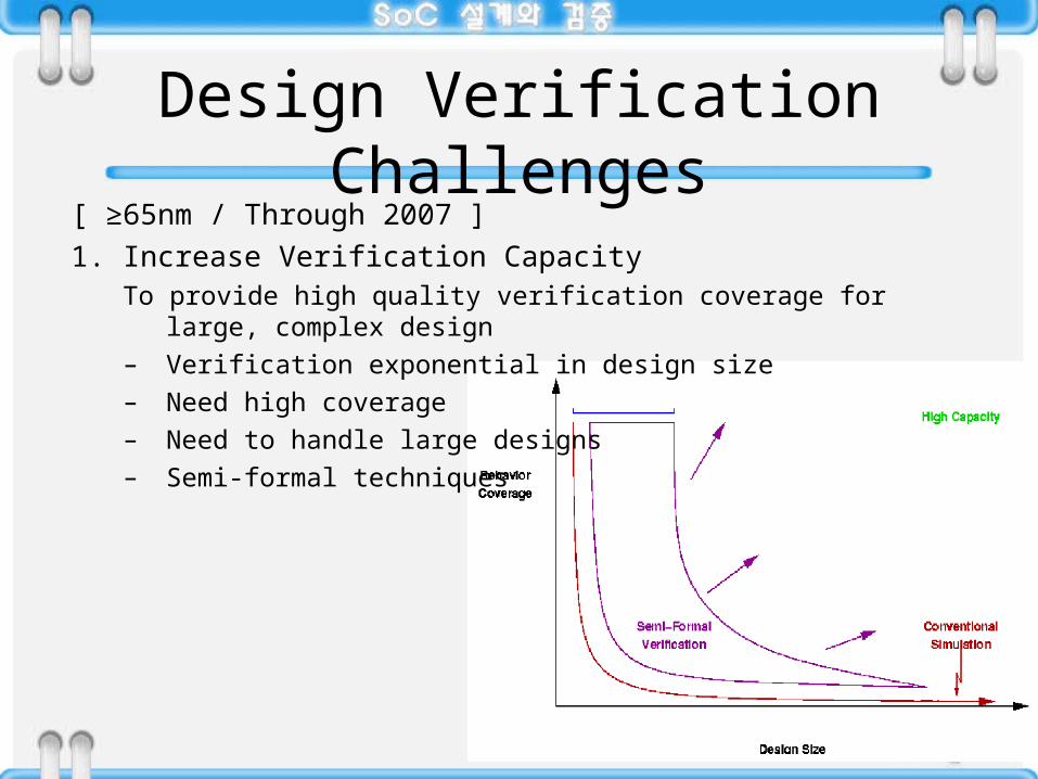
Design Verification Challenges
[ ≥65nm / Through 2007 ]1. Increase Verification Capacity
To provide high quality verification coverage for large, complex design
– Verification exponential in design size– Need high coverage– Need to handle large designs– Semi-formal techniques
46
Design Verification Challenges
2. Robustness verification toolsVerification algorithms highly unpredictable and depend on
highly temperamental heuristics– Improved heuristics for the verification algorithms – Improved characterization of the difficult of verifying a
given design
3. Verification metricsQuantify the quality of a verification effort (a meaningful
notion of coverage)– Behavior coverage– Realistic bug model– Algorithms to determine bug coverage
47
Design Verification Challenges
4. Software verification– Software intrinsically more difficult to verify
• Much of the functionality of SOCs will be defined by software• SW and SW-HW verification is a major SOC verification challenge
– Traditional software verification techniques inapplicable• Hard to verify, due to more complex, dynamic data and enormous state
space• Too labor-intensive to be applicable for SOC
– Verification Integrated hardware/software system– Robust verification methods for software– Design-for-verifiability
48
Design Verification Challenges
5. Verification ReuseVerification Methodology for
• Rapid verification of a system assembled from pre-designed (pre-verified) block
• Near-term: standardized IP interconnects (on-chip buses)
– Must allow reuse of verification of IP blocks– Specify abstract behavior of IP blocks– Specify environmental constraints of IP blocks– Hierarchical verification algorithms
49
Design Verification Challenges
6. Specialized verification methodology– MPU
• Different cost-benefit trade-off• Need exceptionally high capacity• Must be very predictable due to
– Design cycle is very long– Multiple design teams are pipelined
7. Specialized design-for-verifiability– Domain-specific design-for-verifiability techniques
• Self-checking-process, watch-dog processor– Effective in reducing verification cost
• While imposing minimal area and performance penalties
8. New kinds of concurrency– Verification techniques to handle the new forms of
concurrency• Cache coherence, chip-level multiprocessing, simultaneous
multithreading
50
Design Verification Challenges
[ ≤65nm / Beyond 2007 ]1. Design for verifiability
– New methodology needed• Understandings of how design errors occur producing easy-
to-verify design• Sequential testability (scan-based testing)
– Characterize and minimize performance and area impact2. Higher levels of abstraction
– New algorithm needed– Verification methods for the higher-levels of abstraction
• As design moves to a level of abstraction above RTL– Complexity of design enabled by higher-level design– Equivalence checking between the higher-level and lower-
level models
51
Design Verification Challenges
3. Human factors in specification– Specifications of correctness will become unmanageable– Need to understand what kinds of specifications are most
understandable– Need to consider how to make specifications modular and
modifiable
4. Verification of non-digital systems– Hybrid systems verification for analog effects– Hybrid systems verification for analog properties– Verification of probabilistic systems
5. Heterogeneous systems– How to model, analyze, and verify MEMS, EO devices, and
electro-biological device
52
Design Test• High speed device interface
– Faster I/O Speed: multiple GHz– Complex I/O protocol:
• source synchronous, differential, simultaneous bidirection, differential voltage swings
• Highly integrated SOC design– Larger integrated devices
• Non-linear complexity growth for design tools, DFT, manufacturing test– Integration analog, mixed signal
• Nonlinear increase in the cost of testability, design verification, manufacturing test
53
Design Test Challenges[ ≥65nm / Through 2007 ]1. At-speed test with increasing frequencies
– Continuation of at-speed functional test with increased clock frequencies– At-speed structure test with increased clock frequencies– Test and on-chip measurement techniques for multi-GHz serial ports
2. Capacity gap between DFT/Test generation/Fault grading tools and design complexity– Better EDA tools for advanced fault models– DFT to enable low-cost ATE– Non-intrusive logic BIST– AMS DFT/BIST, especially at beyond-baseband frequencies
3. Quality and yield impact due to test equipment limits– Power and thermal management during test– Fault diagnosis and design for diagnosability– Yield improvement and failure analysis tools and methods
54
Design Test Challenges4. Signal integrity testability and new fault models
– Signal integrity testability– Fault modes for analog failures
5. SOC test– Integration of SOC test methods onto test equipment platform– Integration of muliple fabric-specific test methodologies– DFS, BIST and test methods compatible with core-based SOC envir
onment and constraints– Embedded memory built-in self-diagnosis and self-repair – Test reuse
55
Design Test Challenges[ <65nm / Beyond 2007 ]1. Integrated self-testing for heterogeneous SOCs
– Test of multi-GHz RF front end on chip– Use of on-chip programmable resources for SOC self-test– Dependence on self-test solution for SOC– (Analog) signal integrity test issues caused by interference from dig
ital to analog circuitry– Test methods for heterogeneous SOC including MEMS and EO com
ponents
56
Design Test Challenges2. Diagnosis and reliability screens
– Diagnosis and failure analysis for AMS parts– Design for efficient and effective burn-in to screen out latent defect
s– Quality and yield impact due to test equipment limits– New timing-related fault modes for defects/nose in nanometer tec
hnologies
3. Fault tolerance and on-line testing– DFT and fault tolerant design for logic soft errors– Logic self-repair using on-chip reconfigurability– System-level on-line testing


![[ 제 차 ] 경종민 kyung@ee.kaist.ac.kr 1 Overview of SoC Design process.](https://static.fdocument.pub/doc/165x107/56649e055503460f94af16bc/-kyungeekaistackr-1-overview-of-soc-design-process.jpg)


![[ 제 차 ] 경종민 kyung@ee.kaist.ac.kr 1 Platform-based design.](https://static.fdocument.pub/doc/165x107/56649f3a5503460f94c5806f/-kyungeekaistackr-1-platform-based-design.jpg)