VLSI DesignVLSI Design - Sharifce.sharif.edu/courses/91-92/1/ce353-1/resources/root/Lecture...
33
VLSI Design VLSI Design Lecture 7: Transfer Characteristics Lecture 7: Transfer Characteristics, Delay and Power Delay and Power Shaahin Hessabi Shaahin Hessabi Shaahin Hessabi Shaahin Hessabi Department of Computer Engineering Department of Computer Engineering Sharif University of Technology Sharif University of Technology Sharif University of Technology Sharif University of Technology Adapted with modifications from lecture notes prepared Adapted with modifications from lecture notes prepared by the by the book book author (from Prentice Hall PTR) author (from Prentice Hall PTR) Modern VLSI Design 4e: Chapter 3 Sharif University of Technology Slide 1 of 33
-
Upload
trankhuong -
Category
Documents
-
view
219 -
download
0
Transcript of VLSI DesignVLSI Design - Sharifce.sharif.edu/courses/91-92/1/ce353-1/resources/root/Lecture...
VLSI DesignVLSI DesignLecture 7: Transfer CharacteristicsLecture 7: Transfer Characteristics,
Delay and PowerDelay and PowerShaahin HessabiShaahin HessabiShaahin HessabiShaahin Hessabi
Department of Computer EngineeringDepartment of Computer EngineeringSharif University of TechnologySharif University of TechnologySharif University of TechnologySharif University of Technology
Adapted with modifications from lecture notes prepared Adapted with modifications from lecture notes prepared by the by the book book author (from Prentice Hall PTR)author (from Prentice Hall PTR)
Modern VLSI Design 4e: Chapter 3 Sharif University of Technology Slide 1 of 33
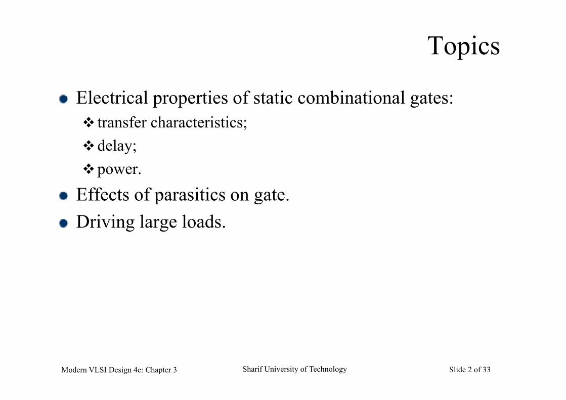
Topics
Electrical properties of static combinational gates: transfer characteristics;delay;power.
Effects of parasitics on gate.Effects of parasitics on gate.Driving large loads.
Modern VLSI Design 4e: Chapter 3 Sharif University of Technology Slide 2 of 33

Logic levels
Solid logic 0/1 defined by VSS/VDD. Inner bounds of logic values VL/VH are not directly determined by circuit properties, as in some other logic y p p , gfamilies.
Vlogic 1
unknown
VDD
VH
Vlogic 0VSS
VL
Modern VLSI Design 4e: Chapter 3 Sharif University of Technology Slide 3 of 33
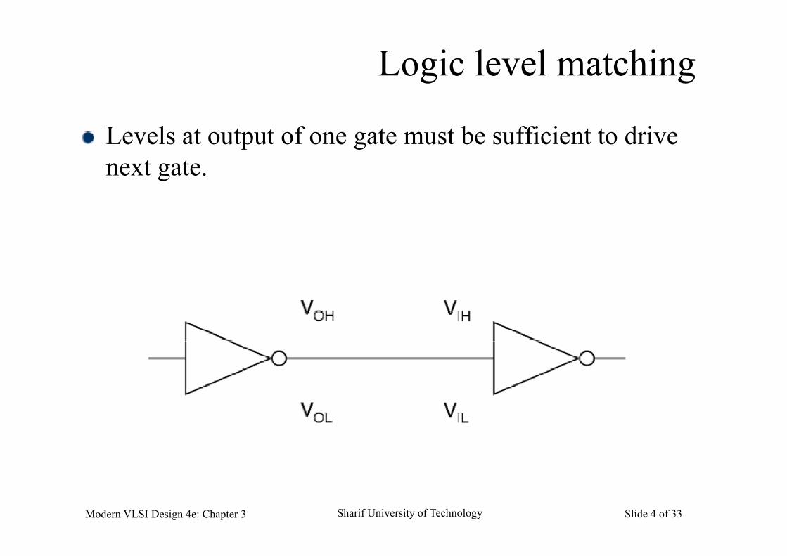
Logic level matching
Levels at output of one gate must be sufficient to drive next gate.
Modern VLSI Design 4e: Chapter 3 Sharif University of Technology Slide 4 of 33

Transfer characteristics
Transfer curve shows static input/output relationship—hold input voltage, measure output voltage.
Modern VLSI Design 4e: Chapter 3 Sharif University of Technology Slide 5 of 33
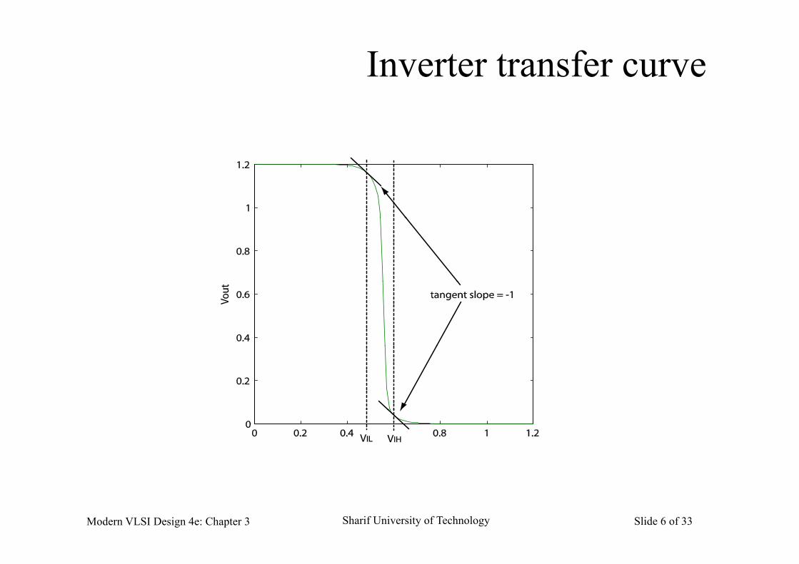
Inverter transfer curve
Modern VLSI Design 4e: Chapter 3 Sharif University of Technology Slide 6 of 33
Logic thresholds
Choose threshold voltages at points where slope of transfer curve = -1.Inverter has a high gain between VIL and VIH points, g g IL IH p ,low gain at outer regions of transfer curve.Note that logic 0 and 1 regions are not equal sized—inNote that logic 0 and 1 regions are not equal sized in this case, high pullup resistance leads to smaller logic 1 rangerange.
Modern VLSI Design 4e: Chapter 3 Sharif University of Technology Slide 7 of 33
Noise margin
Noise margin = voltage difference between output of one gate and input of next. Noise must exceed noise margin to make second gate produce wrong output.In static gates, t= voltages are VDD and VSS, so the output voltages will be acceptable.p g p
Modern VLSI Design 4e: Chapter 3 Sharif University of Technology Slide 8 of 33
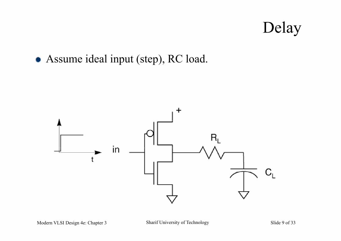
Delay
Assume ideal input (step), RC load.
Modern VLSI Design 4e: Chapter 3 Sharif University of Technology Slide 9 of 33

Delay assumptions
Assume that only one transistor is on at a time. This gives two cases: rise time, pullup on; fall time, pullup off.
Assume resistor model for transistor. ssu e es s o ode o s s o . Ignores saturation region and mischaracterizes linear region,
but results are acceptable.p
Modern VLSI Design 4e: Chapter 3 Sharif University of Technology Slide 10 of 33

Current through transistor
Transistor starts in saturation region, then moves to linear region.
Modern VLSI Design 4e: Chapter 3 Sharif University of Technology Slide 11 of 33

Capacitive load
Most capacitance comesMost capacitance comes from the next gate.L d i dLoad is measured or analyzed by Spice.Cl: unit load capacitance½ load presented by one
minimum-size inverter driving another minimum size inverter
CL = (W/L)i Cl
minimum-size inverter.
Modern VLSI Design 4e: Chapter 3 Sharif University of Technology Slide 12 of 33

Resistive model for transistor
Average V/I at two voltages:g gmaximum output voltagemiddle of linear regionmiddle of linear region
Voltage is Vds, current is given Id at that drain voltage. Step input means that Vgs = VDD always.
Modern VLSI Design 4e: Chapter 3 Sharif University of Technology Slide 13 of 33
S ep pu e s Vgs VDD w ys.

Ways of measuring gate delay
Delay: time required for gate’s output to reach 50% of final value.Transition time: time required for gate’s output to reach q g p10% (logic 0) or 90% (logic 1) of final value.
Modern VLSI Design 4e: Chapter 3 Sharif University of Technology Slide 14 of 33

Inverter delay circuit
Load is resistor + capacitor, driver is resistor.
Modern VLSI Design 4e: Chapter 3 Sharif University of Technology Slide 15 of 33
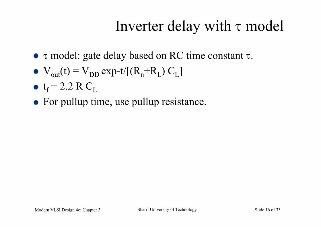
Inverter delay with model
model: gate delay based on RC time constant .Vout(t) = VDD exp-t/[(Rn+RL) CL]tf = 2 2 R CLtf 2.2 R CL
For pullup time, use pullup resistance.
Modern VLSI Design 4e: Chapter 3 Sharif University of Technology Slide 16 of 33
model inverter delay
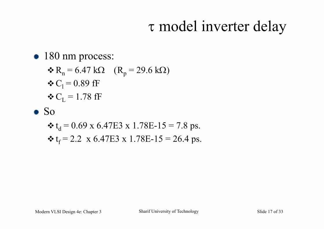
180 nm process: Rn = 6.47 kRp = 29.6 kCl = 0.89 fFl
CL = 1.78 fF
SoSo td = 0.69 x 6.47E3 x 1.78E-15 = 7.8 ps. tf = 2 2 x 6 47E3 x 1 78E-15 = 26 4 ps tf 2.2 x 6.47E3 x 1.78E 15 26.4 ps.
Modern VLSI Design 4e: Chapter 3 Sharif University of Technology Slide 17 of 33

Quality of RC approximation
Modern VLSI Design 4e: Chapter 3 Sharif University of Technology Slide 18 of 33
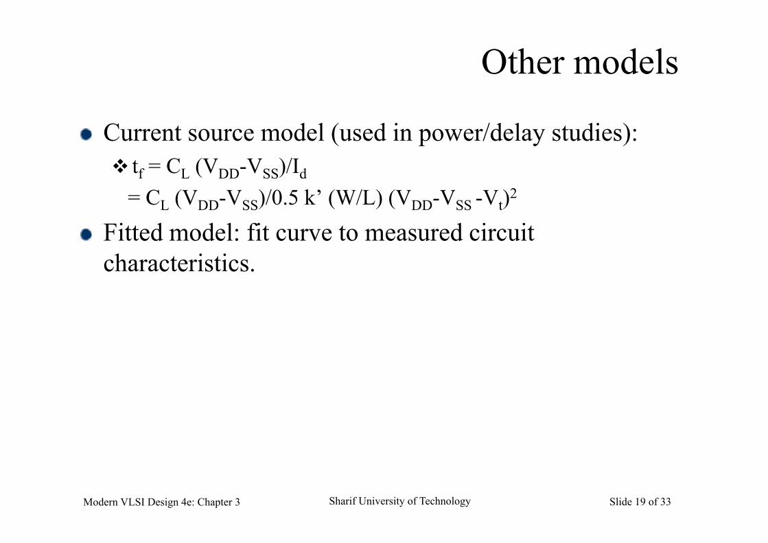
Other models
Current source model (used in power/delay studies): tf = CL (VDD-VSS)/Id
= CL (VDD-VSS)/0.5 k’ (W/L) (VDD-VSS -Vt)2L DD SS DD SS t
Fitted model: fit curve to measured circuit characteristics.c c e s cs.
Modern VLSI Design 4e: Chapter 3 Sharif University of Technology Slide 19 of 33
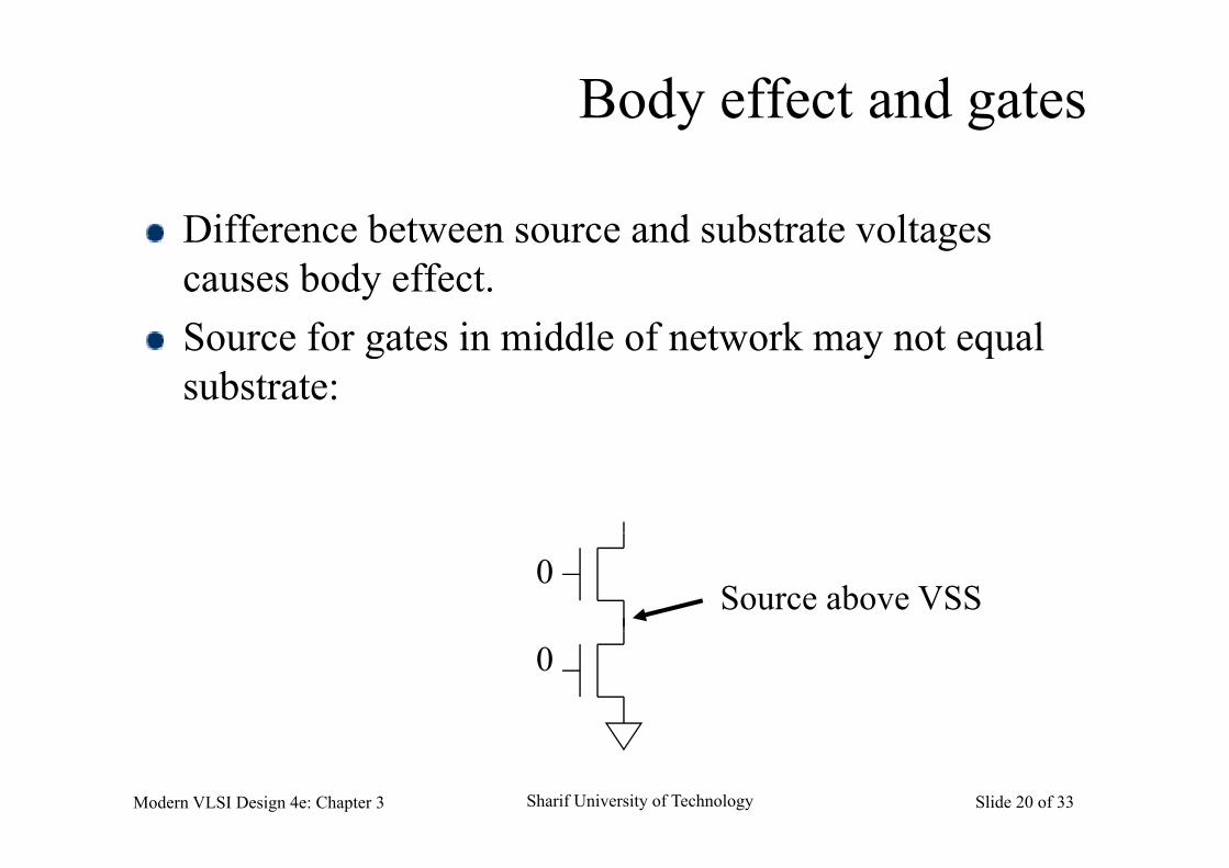
Body effect and gates
Difference between source and substrate voltagesDifference between source and substrate voltages causes body effect.Source for gates in middle of network may not equalSource for gates in middle of network may not equal substrate:
0Source above VSS
0
Modern VLSI Design 4e: Chapter 3 Sharif University of Technology Slide 20 of 33
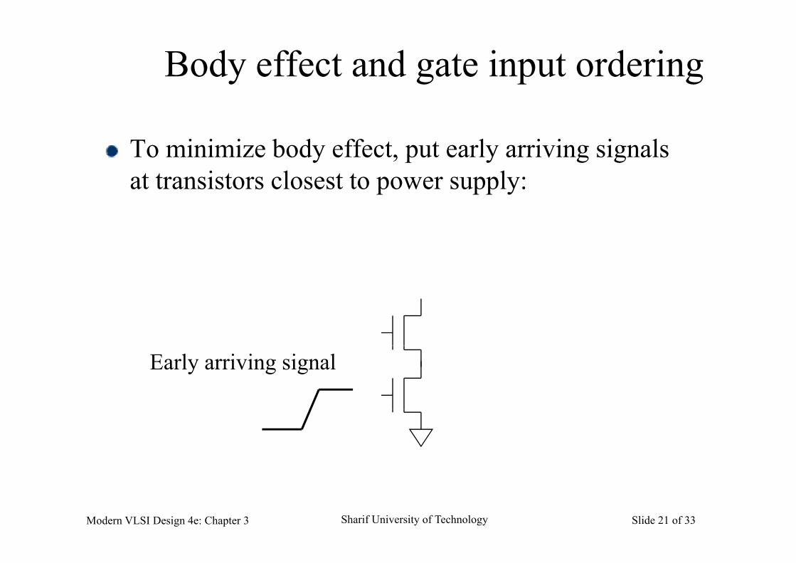
Body effect and gate input ordering
To minimize body effect put early arriving signalsTo minimize body effect, put early arriving signals at transistors closest to power supply:
Early arriving signal
Modern VLSI Design 4e: Chapter 3 Sharif University of Technology Slide 21 of 33
Power consumption analysis
Almost all power consumption comes from switching behavior.Static power dissipation comes from leakage currents.p p gThis small power is important in some very low power
devices, such as implantable medical electronics, telephone chips that obtain power through the phone line, ... .
Surprising result: power consumption is independent of p g p p pthe sizes of the pullups and pulldowns.
Modern VLSI Design 4e: Chapter 3 Sharif University of Technology Slide 22 of 33

Power consumption circuit
Input is square wave, hence, only one transistor is ON p q , , yat a time (the other has a current of a few pico Amps).
Modern VLSI Design 4e: Chapter 3 Sharif University of Technology Slide 23 of 33
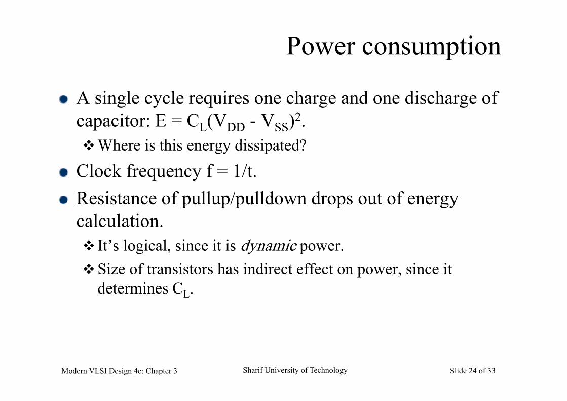
Power consumption
A single cycle requires one charge and one discharge of capacitor: E = CL(VDD - VSS)2.Where is this energy dissipated?
Clock frequency f = 1/t.Resistance of pullup/pulldown drops out of energyResistance of pullup/pulldown drops out of energy calculation. It’s logical since it is dynamic power It s logical, since it is dynamic power.Size of transistors has indirect effect on power, since it
determines CLdetermines CL.
Modern VLSI Design 4e: Chapter 3 Sharif University of Technology Slide 24 of 33
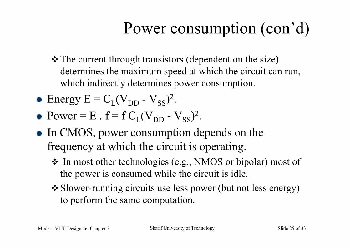
Power consumption (con’d)
The current through transistors (dependent on the size) d i h i d hi h h i idetermines the maximum speed at which the circuit can run, which indirectly determines power consumption.
E E C (V V )2Energy E = CL(VDD - VSS)2.Power = E . f = f CL(VDD - VSS)2.In CMOS, power consumption depends on the frequency at which the circuit is operating.q y p g In most other technologies (e.g., NMOS or bipolar) most of
the power is consumed while the circuit is idle.Slower-running circuits use less power (but not less energy)
to perform the same computation.
Modern VLSI Design 4e: Chapter 3 Sharif University of Technology Slide 25 of 33

Speed-power product
Also known as power-delay product.Helps measure quality of a logic family.For static CMOS:For static CMOS:SP = P/f = CV2.Static CMOS speed power product is independent ofStatic CMOS speed-power product is independent of
operating frequency.Voltage scaling depends on this factVoltage scaling depends on this fact.
Modern VLSI Design 4e: Chapter 3 Sharif University of Technology Slide 26 of 33
Speed-power product (cont’d)
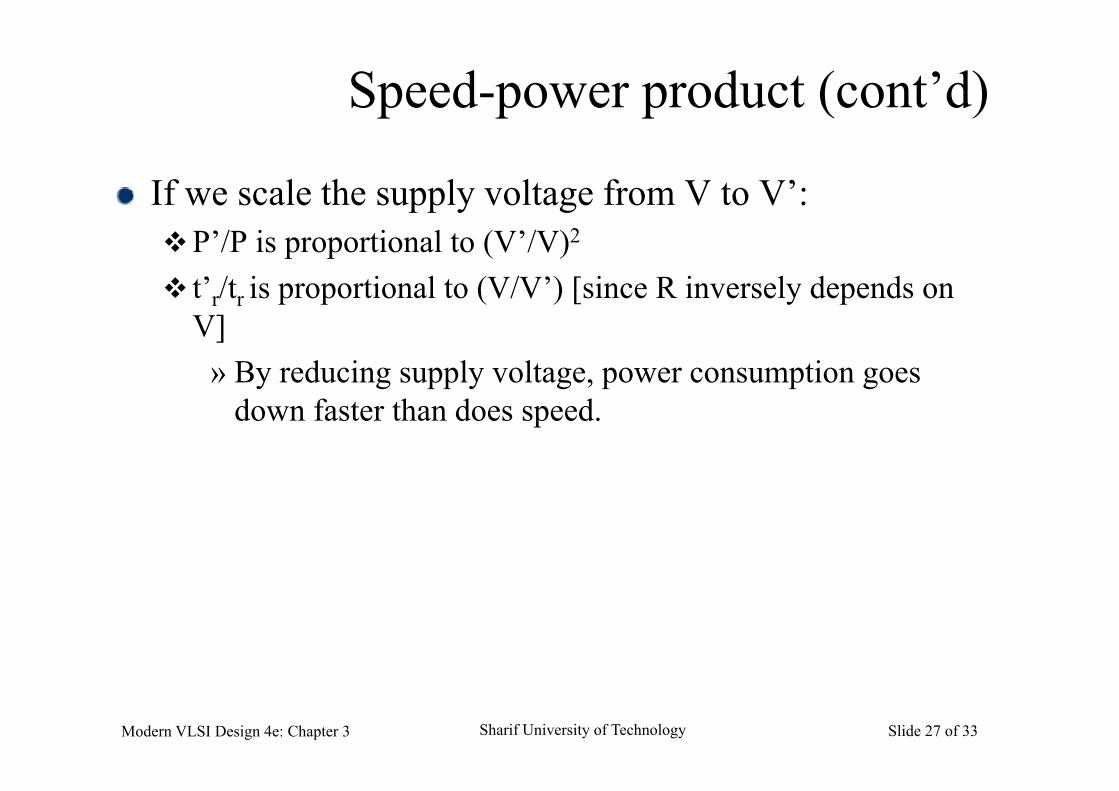
If we scale the supply voltage from V to V’:P’/P is proportional to (V’/V)2
t’r/tr is proportional to (V/V’) [since R inversely depends on r rV]
» By reducing supply voltage, power consumption goes down faster than does speed.
Modern VLSI Design 4e: Chapter 3 Sharif University of Technology Slide 27 of 33

Parasitics and performance
a
b
c
Modern VLSI Design 4e: Chapter 3 Sharif University of Technology Slide 28 of 33
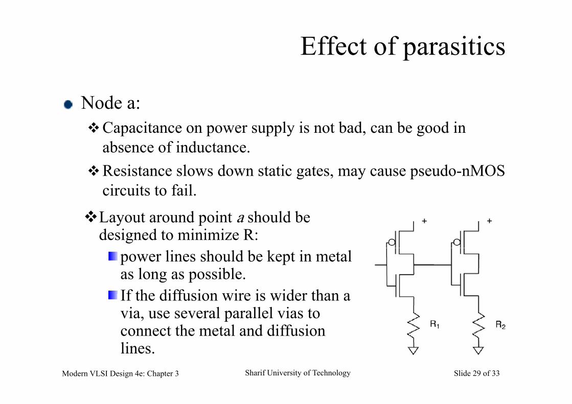
Effect of parasitics
Node a: Capacitance on power supply is not bad, can be good in
absence of inductance. Resistance slows down static gates, may cause pseudo-nMOS
circuits to fail.
Layout around point a should be designed to minimize R:
power lines should be kept in metal as long as possible.If the diffusion wire is wider than aIf the diffusion wire is wider than a via, use several parallel vias to connect the metal and diffusion
Modern VLSI Design 4e: Chapter 3 Sharif University of Technology Slide 29 of 33
lines.
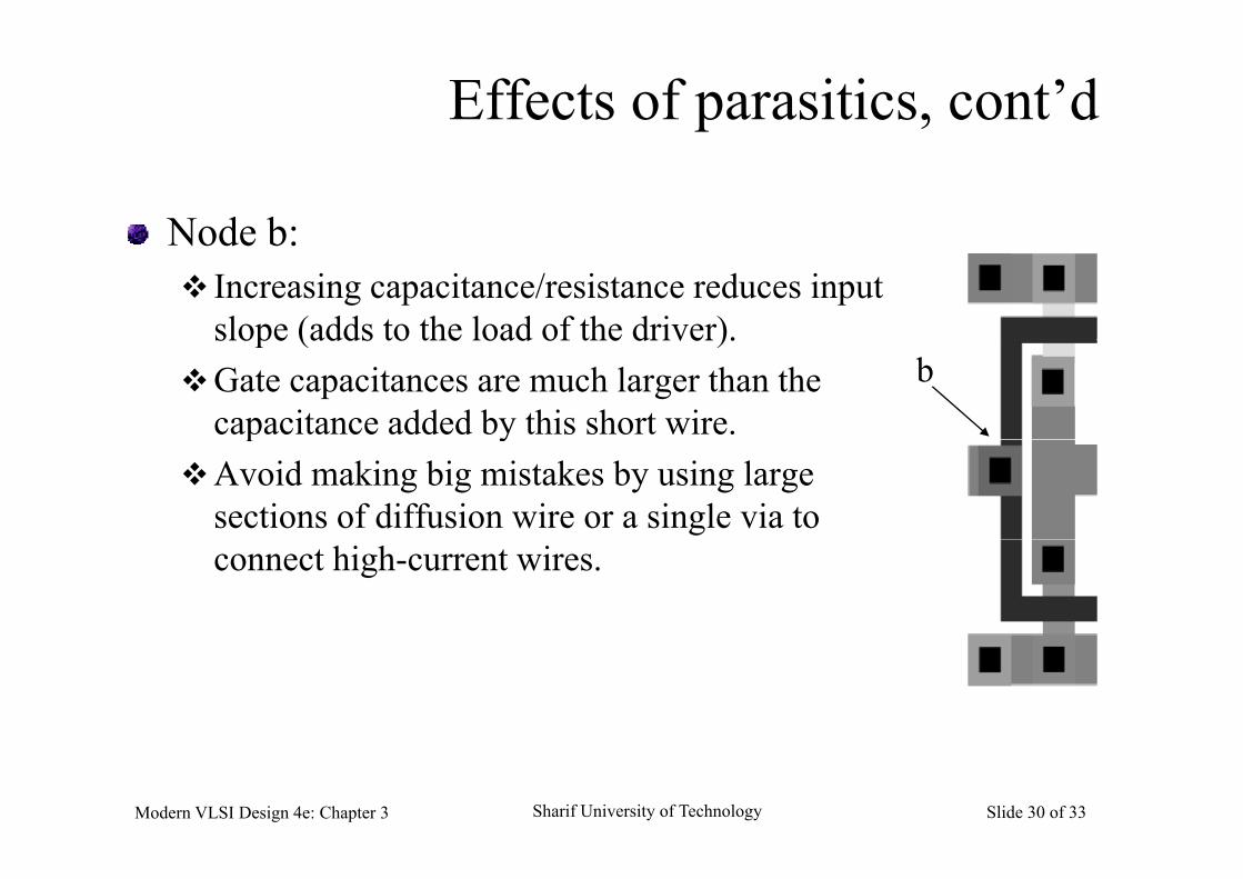
Effects of parasitics, cont’d
Node b:Node b: Increasing capacitance/resistance reduces input
slope (adds to the load of the driver).slope (adds to the load of the driver).Gate capacitances are much larger than the
capacitance added by this short wire.b
p yAvoid making big mistakes by using large
sections of diffusion wire or a single via to connect high-current wires.
Modern VLSI Design 4e: Chapter 3 Sharif University of Technology Slide 30 of 33
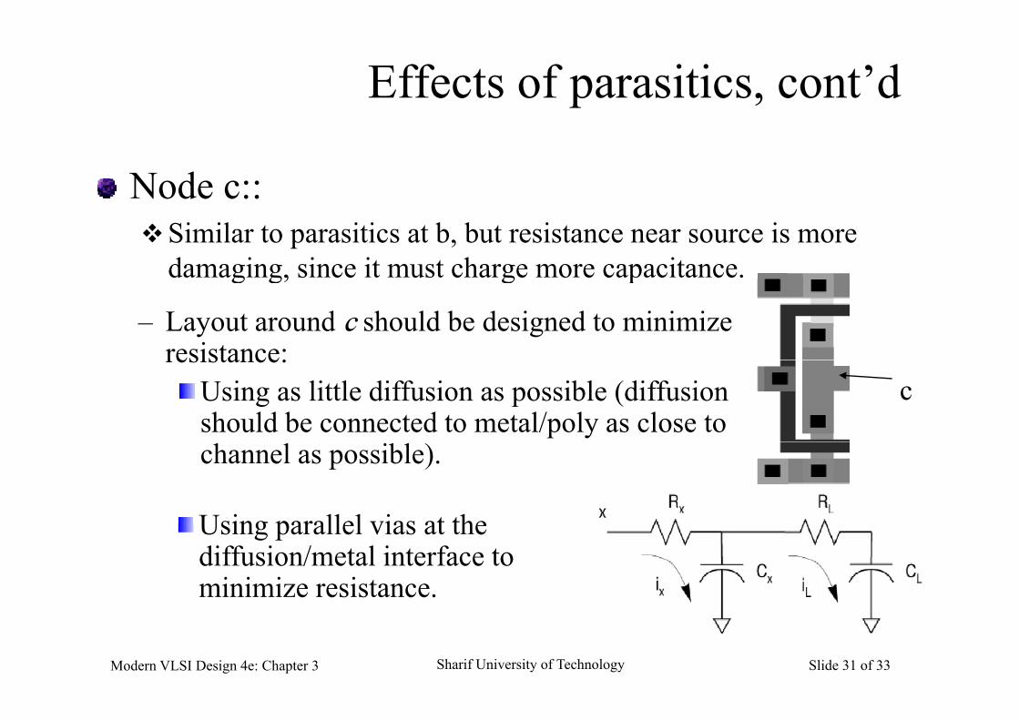
Effects of parasitics, cont’d
Node c::Node c::Similar to parasitics at b, but resistance near source is more
damaging, since it must charge more capacitance.g g, g p
– Layout around c should be designed to minimize resistance:
cresistance:
Using as little diffusion as possible (diffusion should be connected to metal/poly as close to channel as possible).
Using parallel vias at theUsing parallel vias at the diffusion/metal interface to minimize resistance.
Modern VLSI Design 4e: Chapter 3 Sharif University of Technology Slide 31 of 33
Driving large loads
Sometimes, large loads must be driven:off-chip; long wires on-chip (bus). clock wires which go to many points.
This increases the delay.This increases the delay.Sizing up the driver transistors (to increase current) only pushes back the problem; driver now presentsonly pushes back the problem; driver now presents larger capacitance to earlier stage.
Modern VLSI Design 4e: Chapter 3 Sharif University of Technology Slide 32 of 33
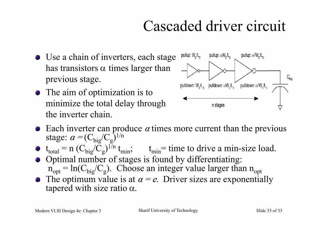
Cascaded driver circuit
Use a chain of inverters, each stage has transistors times larger than previous stage.The aim of optimization is to minimize the total delay through the inverter chainthe inverter chain.Each inverter can produce α times more current than the previous stage: α = (Cbig/Cg)1/nstage: α (Cbig/Cg)ttotal = n (Cbig/Cg)1/n tmin; tmin= time to drive a min-size load.Optimal number of stages is found by differentiating:
l (C /C ) Ch i t l l thnopt = ln(Cbig/Cg). Choose an integer value larger than noptThe optimum value is at α = e. Driver sizes are exponentially tapered with size ratio
Modern VLSI Design 4e: Chapter 3 Sharif University of Technology Slide 33 of 33
p