TXS0206A SD Card Voltage-Translation Transceiver · PDF fileSD/MMC TXS0206A Controller SD/MMC...
32
TXS0206A SD/MMC Controller SD/MMC Card 912345678 Product Folder Sample & Buy Technical Documents Tools & Software Support & Community An IMPORTANT NOTICE at the end of this data sheet addresses availability, warranty, changes, use in safety-critical applications, intellectual property matters and other important disclaimers. PRODUCTION DATA. TXS0206A SCES833B – NOVEMBER 2011 – REVISED APRIL 2016 TXS0206A SD Card Voltage-Translation Transceiver 1 1 Features 1• Level Translator – V CCA and V CCB Range of 1.1 V to 3.6 V – Fast Propagation Delay (4.4 ns Maximum When Translating Between 1.8 V and 3 V) • ESD Protection Exceeds JESD 22 – 2500-V Human-Body Model (A114-B) – 250-V Machine Model (A115-A) – 1500-V Charged-Device Model (C101) 2 Applications • Mobile Phones • Tablet PCs • Notebooks • Ultrabook Computers 3 Description The TXS0206A is a level shifter for interfacing microprocessors with MultiMediaCards (MMCs), secure digital (SD) cards, and Memory Stick™ cards. The voltage-level translator has two supply voltage pins. V CCA as well as V CCB can be operated over the full range of 1.1 V to 3.6 V. The TXS0206A enables system designers to easily interface applications processors or digital basebands to memory cards and SDIO peripherals operating at a different I/O voltage level. The TXS0206A is offered in a 20-bump wafer chip scale package (WCSP). This package has dimensions of 1.96 mm × 1.56 mm, with a 0.4-mm ball pitch for effective board-space savings. Memory cards are widely used in mobile phones, PDAs, digital cameras, personal media players, camcorders, set- top boxes, etc. Low static power consumption and small package size make the TXS0206A an ideal choice for these applications. Device Information (1) PART NUMBER PACKAGE BODY SIZE TXS0206A DSBGA (20) 1.96 mm × 1.56 mm (1) For all available packages, see the orderable addendum at the end of the data sheet. Application Example
Transcript of TXS0206A SD Card Voltage-Translation Transceiver · PDF fileSD/MMC TXS0206A Controller SD/MMC...

TXS0206ASD/MMCController
SD/MMCCard
91
23
45
67
8
Product
Folder
Sample &Buy
Technical
Documents
Tools &
Software
Support &Community
An IMPORTANT NOTICE at the end of this data sheet addresses availability, warranty, changes, use in safety-critical applications,intellectual property matters and other important disclaimers. PRODUCTION DATA.
TXS0206ASCES833B –NOVEMBER 2011–REVISED APRIL 2016
TXS0206A SD Card Voltage-Translation Transceiver
1
1 Features1• Level Translator
– VCCA and VCCB Range of 1.1 V to 3.6 V– Fast Propagation Delay (4.4 ns Maximum
When Translating Between 1.8 V and 3 V)• ESD Protection Exceeds JESD 22
– 2500-V Human-Body Model (A114-B)– 250-V Machine Model (A115-A)– 1500-V Charged-Device Model (C101)
2 Applications• Mobile Phones• Tablet PCs• Notebooks• Ultrabook Computers
3 DescriptionThe TXS0206A is a level shifter for interfacingmicroprocessors with MultiMediaCards (MMCs),secure digital (SD) cards, and Memory Stick™ cards.
The voltage-level translator has two supply voltagepins. VCCA as well as VCCB can be operated over thefull range of 1.1 V to 3.6 V. The TXS0206A enablessystem designers to easily interface applicationsprocessors or digital basebands to memory cards andSDIO peripherals operating at a different I/O voltagelevel.
The TXS0206A is offered in a 20-bump wafer chipscale package (WCSP). This package hasdimensions of 1.96 mm × 1.56 mm, with a 0.4-mmball pitch for effective board-space savings. Memorycards are widely used in mobile phones, PDAs, digitalcameras, personal media players, camcorders, set-top boxes, etc. Low static power consumption andsmall package size make the TXS0206A an idealchoice for these applications.
Device Information(1)
PART NUMBER PACKAGE BODY SIZETXS0206A DSBGA (20) 1.96 mm × 1.56 mm
(1) For all available packages, see the orderable addendum atthe end of the data sheet.
Application Example

2
TXS0206ASCES833B –NOVEMBER 2011–REVISED APRIL 2016 www.ti.com
Product Folder Links: TXS0206A
Submit Documentation Feedback Copyright © 2011–2016, Texas Instruments Incorporated
Table of Contents1 Features .................................................................. 12 Applications ........................................................... 13 Description ............................................................. 14 Revision History..................................................... 25 Pin Configuration and Functions ......................... 36 Specifications......................................................... 4
6.1 Absolute Maximum Ratings ...................................... 46.2 ESD Ratings ............................................................ 46.3 Recommended Operating Conditions....................... 56.4 Thermal Information .................................................. 66.5 Electrical Characteristics........................................... 66.6 Timing Requirements—VCCA = 1.2 V ± 0.1 V........... 76.7 Timing Requirements—VCCA = 1.8 V ± 0.15 V......... 86.8 Timing Requirements—VCCA = 3.3 V ± 0.3 V........... 86.9 Switching Characteristics—VCCA = 1.2 V ± 0.1 V .... 96.10 Switching Characteristics—VCCA = 1.8 V ± 0.15 V
................................................................................. 106.11 Switching Characteristics—VCCA = 3.3 V ± 0.3 V. 116.12 Operating Characteristics —VCCA = 1.2 V ............ 126.13 Operating Characteristics —VCCA = 1.8 V ............ 136.14 Operating Characteristics — VCCA = 3.3 V........... 136.15 Typical Characteristics .......................................... 14
7 Parameter Measurement Information ................ 158 Detailed Description ............................................ 16
8.1 Overview ................................................................. 168.2 Functional Block Diagram ....................................... 168.3 Feature Description................................................. 178.4 Device Functional Modes........................................ 18
9 Application and Implementation ........................ 199.1 Application Information............................................ 199.2 Typical Application ................................................. 199.3 System Examples ................................................... 21
10 Power Supply Recommendations ..................... 2211 Layout................................................................... 22
11.1 Layout Guidelines ................................................. 2211.2 Layout Example .................................................... 23
12 Device and Documentation Support ................. 2412.1 Documentation Support ....................................... 2412.2 Community Resources.......................................... 2412.3 Trademarks ........................................................... 2412.4 Electrostatic Discharge Caution............................ 2412.5 Glossary ................................................................ 24
13 Mechanical, Packaging, and OrderableInformation ........................................................... 24
4 Revision HistoryNOTE: Page numbers for previous revisions may differ from page numbers in the current version.
Changes from Revision A (May 2012) to Revision B Page
• Added Device Information table, ESD Ratings table, Feature Description section, Device Functional Modes,Application and Implementation section, Power Supply Recommendations section, Layout section, Device andDocumentation Support section, and Mechanical, Packaging, and Orderable Information section. .................................... 1
• Deleted the ordering information. See POA at the end of the datasheet............................................................................... 1

D
E
A
1 2 3 4
B
C
3
TXS0206Awww.ti.com SCES833B –NOVEMBER 2011–REVISED APRIL 2016
Product Folder Links: TXS0206A
Submit Documentation FeedbackCopyright © 2011–2016, Texas Instruments Incorporated
5 Pin Configuration and Functions
YFP Package20–Pin DSBGA
Top View
Pin Assignments1 2 3 4
A DAT2A VCCA WP DAT2BB DAT3A CD VCCB DAT3BC CMDA GND GND CMDBD DAT0A CLKA CLKB DAT0BE DAT1A CLK-f EN DAT1B
Pin FunctionsPIN
TYPE DESCRIPTIONNO. NAMEA1 DAT2A I/O Data bit 2 connected to host. Referenced to VCCA. Includes a 40-kΩ pullup resistor to VCCA.
A2 VCCA Pwr A-port supply voltage. VCCA powers all A-port I/Os and control inputs.
A3 WP O Connected to write protect on the mechanical connector. The WP pin has an internal 100-kΩ (± 30%)pullup resistor to VCCA. Leave unconnected if not used.
A4 DAT2B I/O Data bit 2 connected to memory card. Referenced to VCCB. Includes a 40-kΩ pullup resistor to VCCB.B1 DAT3A I/O Data bit 3 connected to host. Referenced to VCCA. Includes a 40-kΩ pullup resistor to VCCA.
B2 CD O Connected to card detect on the mechanical connector. The CD pin has an internal 100-kΩ (± 30%)pullup resistor to VCCA. Leave unconnected if not used.
B3 VCCB Pwr B-port supply voltage. VCCB powers all B-port I/Os.B4 DAT3B I/O Data bit 3 connected to memory card. Referenced to VCCB. Includes a 40-kΩ pullup resistor to VCCB.C1 CMDA I/O Command bit connected to host. Referenced to VCCA. Includes a 40-kΩ pullup resistor to VCCA.C2 GND — GroundC3 GND — GroundC4 CMDB I/O Command bit connected to memory card. Referenced to VCCB. Includes a 40-kΩ pullup resistor to VCCB.D1 DAT0A I/O Data bit 0 connected to host. Referenced to VCCA. Includes a 40-kΩ pullup resistor to VCCA.D2 CLKA I Clock signal connected to host. Referenced to VCCA.D3 CLKB O Clock signal connected to memory card. Referenced to VCCB.D4 DAT0B I/O Data bit 0 connected to memory card. Referenced to VCCB. Includes a 40-kΩ pullup resistor to VCCB.E1 DAT1A I/O Data bit 1 connected to host. Referenced to VCCA. Includes a 40-kΩ pullup resistor to VCCA.E2 CLK-f O Clock feedback to host for resynchronizing data to a processor. Leave unconnected if not used.E3 EN I Enable/disable control. Pull EN low to place all outputs in Hi-Z state. Referenced to VCCA.E4 DAT1B I/O Data bit 1 connected to memory card. Referenced to VCCB. Includes a 40-kΩ pullup resistor to VCCB.
4
TXS0206ASCES833B –NOVEMBER 2011–REVISED APRIL 2016 www.ti.com
Product Folder Links: TXS0206A
Submit Documentation Feedback Copyright © 2011–2016, Texas Instruments Incorporated
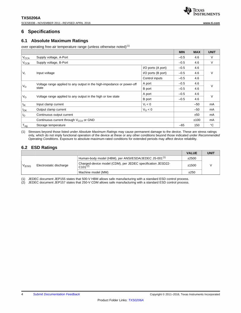
(1) Stresses beyond those listed under Absolute Maximum Ratings may cause permanent damage to the device. These are stress ratingsonly, which do not imply functional operation of the device at these or any other conditions beyond those indicated under RecommendedOperating Conditions. Exposure to absolute-maximum-rated conditions for extended periods may affect device reliability.
6 Specifications
6.1 Absolute Maximum Ratingsover operating free-air temperature range (unless otherwise noted) (1)
MIN MAX UNITVCCA Supply voltage, A-Port –0.5 4.6 VVCCB Supply voltage, B-Port –0.5 4.6 V
VI Input voltageI/O ports (A port) –0.5 4.6
VI/O ports (B port) –0.5 4.6Control inputs –0.5 4.6
VOVoltage range applied to any output in the high-impedance or power-offstate
A port –0.5 4.6V
B port –0.5 4.6
VO Voltage range applied to any output in the high or low stateA port –0.5 4.6
VB port –0.5 4.6
IIK Input clamp current VI < 0 –50 mAIOK Output clamp current VO < 0 –50 mAIO Continuous output current ±50 mA
Continuous current through VCCA or GND ±100 mATstg Storage temperature –65 150 °C
(1) JEDEC document JEP155 states that 500-V HBM allows safe manufacturing with a standard ESD control process.(2) JEDEC document JEP157 states that 250-V CDM allows safe manufacturing with a standard ESD control process.
6.2 ESD RatingsVALUE UNIT
V(ESD) Electrostatic discharge
Human-body model (HBM), per ANSI/ESDA/JEDEC JS-001 (1) ±2500
VCharged-device model (CDM), per JEDEC specification JESD22-C101 (2) ±1500
Machine model (MM) ±250

5
TXS0206Awww.ti.com SCES833B –NOVEMBER 2011–REVISED APRIL 2016
Product Folder Links: TXS0206A
Submit Documentation FeedbackCopyright © 2011–2016, Texas Instruments Incorporated
(1) All unused data inputs of the device must be held at VCCI or GND to ensure proper device operation. Refer to the TI application report,Implications of Slow or Floating CMOS Inputs, SCBA004.
6.3 Recommended Operating ConditionsSee (1)
VCCA VCCB MIN MAX UNITVCCA Supply voltage 1.1 3.6 VVCCB Supply voltage 1.1 3.6 V
VIHHigh-level inputvoltage
A-Port CMD andDATA I/OsB-Port CMD andDATA I/Os
1.1 V to 1.95 V 1.1 V to 1.95 V
VCCI – 0.2 VCCI V1.95 V to 3.6 V 1.95 V to 3.6 V
EN and CLKA 1.1 V to 3.6 V 1.1 V to 3.6 V VCCI × 0.65 VCCI
VILLow-level inputvoltage
A-Port CMD andDATA I/OsB-Port CMD andDATA I/Os
1.1 V to 1.95 V 1.1 V to 1.95 V
0 0.15V1.95 V to 3.6 V 1.95 V to 3.6 V
EN and CLKA 1.1 V to 3.6 V 1.1 V to 3.6 V 0 VCCI × 0.35
VO Output voltageActive state 0 VCCO V3-state 0 3.6
IOH High-level output current (CLK-f output)
1.1 V to 3.6 V
1.1 V to 3.6 V
–100 µA1.1 V to 1.3 V –0.5
mA1.4 V to 1.6 V –1
1.65 V to 1.95 V –22.3 V to 2.7 V –43 V to 3.6 V –8
IOL Low-level output current (CLK-f output)
1.1 V to 3.6 V
1.1 V to 3.6 V
100 μA1.1 V to 1.3 V 0.5
mA1.4 V to 1.6 V 1
1.65 V to 1.95 V 22.3 V to 2.7 V 43 V to 3.6 V 8
IOH High-level output current (CLK output) 1.1 V to 3.6 V
1.1 V to 3.6 V –100 μA1.1 V to 1.3 V –0.5
mA1.4 V to 1.6 V –1
1.65 V to 1.95 V –22.3 V to 2.7 V –43 V to 3.6 V –8
IOL Low-level output current (CLK output) 1.1 V to 3.6 V
1.1 V to 3.6 V 100 µA1.1 V to 1.3 V 0.5
mA1.4 V to 1.6 V 1
1.65 V to 1.95 V 22.3 V to 2.7 V 43 V to 3.6 V 8
Δt/Δv Input transition rise or fall rate 5 ns/VTA Operating free-air temperature –40 85 °C
6
TXS0206ASCES833B –NOVEMBER 2011–REVISED APRIL 2016 www.ti.com
Product Folder Links: TXS0206A
Submit Documentation Feedback Copyright © 2011–2016, Texas Instruments Incorporated
(1) For more information about traditional and new thermal metrics, see the Semiconductor and IC Package Thermal Metrics applicationreport, SPRA953.
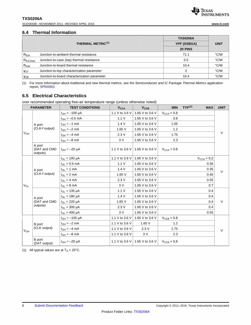
6.4 Thermal Information
THERMAL METRIC (1)TXS0206A
UNITYFP (DSBGA)20 PINS
RθJA Junction-to-ambient thermal resistance 71.1 °C/WRθJC(top) Junction-to-case (top) thermal resistance 0.5 °C/WRθJB Junction-to-board thermal resistance 10.4 °C/WψJT Junction-to-top characterization parameter 2 °C/WψJB Junction-to-board characterization parameter 10.4 °C/W
(1) All typical values are at TA = 25°C.
6.5 Electrical Characteristicsover recommended operating free-air temperature range (unless otherwise noted)
PARAMETER TEST CONDITIONS VCCA VCCB MIN TYP (1) MAX UNIT
VOH
A port(CLK-f output)
IOH = –100 μA 1.1 V to 3.6 V 1.65 V to 3.6 V VCCA × 0.8
V
IOH = –0.5 mA 1.1 V 1.65 V to 3.6 V 0.8IOH = –1 mA 1.4 V 1.65 V to 3.6 V 1.05IOH = –2 mA 1.65 V 1.65 V to 3.6 V 1.2IOH = –4 mA 2.3 V 1.65 V to 3.6 V 1.75IOH = –8 mA 3 V 1.65 V to 3.6 V 2.3
A port(DAT and CMDoutputs)
IOH = –20 μA 1.1 V to 3.6 V 1.65 V to 3.6 V VCCA × 0.8
VOL
A port(CLK-f output)
IOL = 100 μA 1.1 V to 3.6 V 1.65 V to 3.6 V VCCA × 0.2
V
IOL = 0.5 mA 1.1 V 1.65 V to 3.6 V 0.35IOL = 1 mA 1.4 V 1.65 V to 3.6 V 0.35IOL = 2 mA 1.65 V 1.65 V to 3.6 V 0.45IOL = 4 mA 2.3 V 1.65 V to 3.6 V 0.55IOL = 8 mA 3 V 1.65 V to 3.6 V 0.7
A port(DAT and CMDoutputs)
IOL = 135 μA 1.1 V 1.65 V to 3.6 V 0.4
VIOL = 180 μA 1.4 V 1.65 V to 3.6 V 0.4IOL = 220 μA 1.65 V 1.65 V to 3.6 V 0.4IOL = 300 μA 2.3 V 1.65 V to 3.6 V 0.4IOL = 400 μA 3 V 1.65 V to 3.6 V 0.55
VOH
B port(CLK output)
IOH = –100 μA 1.1 V to 3.6 V 1.65 V to 3.6 V VCCB × 0.8
V
IOH = –2 mA 1.1 V to 3.6 V 1.65 V 1.2IOH = –4 mA 1.1 V to 3.6 V 2.3 V 1.75IOH = –8 mA 1.1 V to 3.6 V 3 V 2.3
B port(DAT output) IOH = –20 μA 1.1 V to 3.6 V 1.65 V to 3.6 V VCCB × 0.8

7
TXS0206Awww.ti.com SCES833B –NOVEMBER 2011–REVISED APRIL 2016
Product Folder Links: TXS0206A
Submit Documentation FeedbackCopyright © 2011–2016, Texas Instruments Incorporated
Electrical Characteristics (continued)over recommended operating free-air temperature range (unless otherwise noted)
PARAMETER TEST CONDITIONS VCCA VCCB MIN TYP (1) MAX UNIT
VOL
B port
IOL = 100 μA 1.1 V to 3.6 V 1.65 V to 3.6 V VCCB × 0.2
VIOL = 2 mA 1.1 V to 3.6 V 1.65 V 0.45IOL = 4 mA 1.1 V to 3.6 V 2.3 V 0.55IOL = 8 mA 1.1 V to 3.6 V 3 V 0.7
B port(DAT output)
IOL = 135 μA 1.1 V to 3.6 V 1.65 V to 3.6 V 0.4
VIOL = 220 μA 1.1 V to 3.6 V 1.65 V 0.4IOL = 300 μA 1.1 V to 3.6 V 2.3 V 0.4IOL = 300 μA 1.1 V to 3.6 V 3 V 0.55
II Control inputs VI = VCCA or GND 1.1 V to 3.6 V 1.65 V to 3.6 V ±1 μAICCA A port VI = VCCI, IO = 0 1.1 V to 3.6 V 1.65 V to 3.6 V 7 μAICCB B port VI = VCCI, IO = 0 1.1 V to 3.6 V 1.65 V to 3.6 V 11 μA
CioA port 5.5 6.5
pFB port 7 9.5
CiControl inputs VI = VCCA or GND 3.5 4.5
pFClock input VI = VCCA or GND 3 4
6.6 Timing Requirements—VCCA = 1.2 V ± 0.1 Vover recommended operating free-air temperature range (unless otherwise noted)
VCC MIN MAX UNIT
Data rate
Command
Push-pulldriving
VCCB = 1.8 V ± 0.15 V 40
MbpsVCCB = 3.3 V ± 0.3 V 40
Open-draindriving
VCCB = 1.8 V ± 0.15 V 1VCCB = 3.3 V ± 0.3 V 1
ClockPush-pull
driving
VCCB = 1.8 V ± 0.15 V 40MHz
VCCB = 3.3 V ± 0.3 V 40
DataVCCB = 1.8 V ± 0.15 V 40
MbpsVCCB = 3.3 V ± 0.3 V 40
tWPulse
duration
Command
Push-pulldriving
VCCB = 1.8 V ± 0.15 V 25ns
VCCB = 3.3 V ± 0.3 V 25
Open-draindriving
VCCB = 1.8 V ± 0.15 V 1µs
VCCB = 3.3 V ± 0.3 V 1
ClockPush-pull
driving
VCCB = 1.8 V ± 0.15 V 10ns
VCCB = 3.3 V ± 0.3 V 8.3
DataVCCB = 1.8 V ± 0.15 V 25
nsVCCB = 3.3 V ± 0.3 V 25

8
TXS0206ASCES833B –NOVEMBER 2011–REVISED APRIL 2016 www.ti.com
Product Folder Links: TXS0206A
Submit Documentation Feedback Copyright © 2011–2016, Texas Instruments Incorporated
6.7 Timing Requirements—VCCA = 1.8 V ± 0.15 Vover recommended operating free-air temperature range (unless otherwise noted)
VCC MIN MAX UNIT
Data rate
Command
Push-pulldriving
VCCB = 1.8 V ± 0.15 V 60
MbpsVCCB = 3.3 V ± 0.3 V 60
Open-draindriving
VCCB = 1.8 V ± 0.15 V 1VCCB = 3.3 V ± 0.3 V 1
ClockPush-pull
driving
VCCB = 1.8 V ± 0.15 V 60MHz
VCCB = 3.3 V ± 0.3 V 60
DataVCCB = 1.8 V ± 0.15 V 60
MbpsVCCB = 3.3 V ± 0.3 V 60
tWPulse
duration
Command
Push-pulldriving
VCCB = 1.8 V ± 0.15 V 17ns
VCCB = 3.3 V ± 0.3 V 17
Open-draindriving
VCCB = 1.8 V ± 0.15 V 1µs
VCCB = 3.3 V ± 0.3 V 1
ClockPush-pull
driving
VCCB = 1.8 V ± 0.15 V 8.3ns
VCCB = 3.3 V ± 0.3 V 8.3
DataVCCB = 1.8 V ± 0.15 V 17
nsVCCB = 3.3 V ± 0.3 V 17
6.8 Timing Requirements—VCCA = 3.3 V ± 0.3 Vover recommended operating free-air temperature range (unless otherwise noted)
VCC MIN MAX UNIT
Data rate
Command
Push-pulldriving
VCCB = 1.8 V ± 0.15 V 60
MbpsVCCB = 3.3 V ± 0.3 V 60
Open-draindriving
VCCB = 1.8 V ± 0.15 V 1VCCB = 3.3 V ± 0.3 V 1
ClockPush-pull
driving
VCCB = 1.8 V ± 0.15 V 55MHz
VCCB = 3.3 V ± 0.3 V 55
DataVCCB = 1.8 V ± 0.15 V 60
MbpsVCCB = 3.3 V ± 0.3 V 60
tWPulse
duration
Command
Push-pulldriving
VCCB = 1.8 V ± 0.15 V 17ns
VCCB = 3.3 V ± 0.3 V 17
Open-draindriving
VCCB = 1.8 V ± 0.15 V 1µs
VCCB = 3.3 V ± 0.3 V 1
ClockPush-pull
driving
VCCB = 1.8 V ± 0.15 V 9ns
VCCB = 3.3 V ± 0.3 V 9
DataVCCB = 1.8 V ± 0.15 V 17
nsVCCB = 3.3 V ± 0.3 V 17

9
TXS0206Awww.ti.com SCES833B –NOVEMBER 2011–REVISED APRIL 2016
Product Folder Links: TXS0206A
Submit Documentation FeedbackCopyright © 2011–2016, Texas Instruments Incorporated
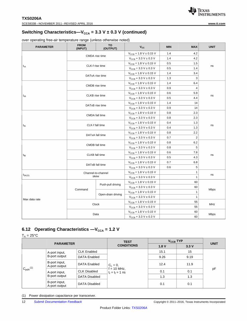
6.9 Switching Characteristics—VCCA = 1.2 V ± 0.1 Vover operating free-air temperature range (unless otherwise noted)
PARAMETER FROM(INPUT)
TO(OUTPUT) VCC MIN MAX UNIT
tpd
CMDA CMDBVCCB = 1.8 V ± 0.15 V 5.7
ns
VCCB = 3.3 V ± 0.3 V 4.4
CMDB CMDAVCCB = 1.8 V ± 0.15 V 6.7
VCCB = 3.3 V ± 0.3 V 5.8
CLKA CLKBVCCB = 1.8 V ± 0.15 V 6.2
VCCB = 3.3 V ± 0.3 V 4.5
DATxA DATxBVCCB = 1.8 V ± 0.15 V 7.6
VCCB = 3.3 V ± 0.3 V 7.5
DATxB DATxAVCCB = 1.8 V ± 0.15 V 6.3
VCCB = 3.3 V ± 0.3 V 4.6
CLKA CLK-fVCCB = 1.8 V ± 0.15 V 12
VCCB = 3.3 V ± 0.3 V 7.9
ten
EN B-portVCCB = 1.8 V ± 0.15 V 1
µsVCCB = 3.3 V ± 0.3 V 1
EN A-portVCCB = 1.8 V ± 0.15 V 1
VCCB = 3.3 V ± 0.3 V 1
tdis
EN B-portVCCB = 1.8 V ± 0.15 V 412
nsVCCB = 3.3 V ± 0.3 V 363
EN A-portVCCB = 1.8 V ± 0.15 V 423
VCCB = 3.3 V ± 0.3 V 422
trA
CMDA rise timeVCCB = 1.8 V ± 0.15 V 3.5 8.4
ns
VCCB = 3.3 V ± 0.3 V 3.4 8.1
CLK-f rise timeVCCB = 1.8 V ± 0.15 V 1 4.7
VCCB = 3.3 V ± 0.3 V 1 4.1
DATxA rise timeVCCB = 1.8 V ± 0.15 V 3.5 8.4
VCCB = 3.3 V ± 0.3 V 3.4 8.1
trB
CMDB rise timeVCCB = 1.8 V ± 0.15 V 1.4 6.5
ns
VCCB = 3.3 V ± 0.3 V 0.6 3.1
CLKB rise timeVCCB = 1.8 V ± 0.15 V 0.6 5.9
VCCB = 3.3 V ± 0.3 V 0.5 4.3
DATxB rise timeVCCB = 1.8 V ± 0.15 V 1.4 10.9
VCCB = 3.3 V ± 0.3 V 0.6 5
tfA
CMDA fall timeVCCB = 1.8 V ± 0.15 V 2.4 5.7
ns
VCCB = 3.3 V ± 0.3 V 2 5.1
CLK-f fall timeVCCB = 1.8 V ± 0.15 V 0.8 2.5
VCCB = 3.3 V ± 0.3 V 0.8 3
DATxA fall timeVCCB = 1.8 V ± 0.15 V 2.4 5.7
VCCB = 3.3 V ± 0.3 V 1.9 5.1
tfB
CMDB fall timeVCCB = 1.8 V ± 0.15 V 1.2 5.4
ns
VCCB = 3.3 V ± 0.3 V 0.6 3.6
CLKB fall timeVCCB = 1.8 V ± 0.15 V 0.6 6.3
VCCB = 3.3 V ± 0.3 V 0.5 4
DATxB fall timeVCCB = 1.8 V ± 0.15 V 0.6 6.3
VCCB = 3.3 V ± 0.3 V 0.5 3.6
tSK(O)Channel-to-channel
skewVCCB = 1.8 V ± 0.15 V 1
nsVCCB = 3.3 V ± 0.3 V 1

10
TXS0206ASCES833B –NOVEMBER 2011–REVISED APRIL 2016 www.ti.com
Product Folder Links: TXS0206A
Submit Documentation Feedback Copyright © 2011–2016, Texas Instruments Incorporated
Switching Characteristics—VCCA = 1.2 V ± 0.1 V (continued)over operating free-air temperature range (unless otherwise noted)
PARAMETER FROM(INPUT)
TO(OUTPUT) VCC MIN MAX UNIT
Max data rate
Command
Push-pull drivingVCCB = 1.8 V ± 0.15 V 40
MbpsVCCB = 3.3 V ± 0.3 V 40
Open-drain drivingVCCB = 1.8 V ± 0.15 V 1
VCCB = 3.3 V ± 0.3 V 1
ClockVCCB = 1.8 V ± 0.15 V 40
MHzVCCB = 3.3 V ± 0.3 V 60
DataVCCB = 1.8 V ± 0.15 V 40
MbpsVCCB = 3.3 V ± 0.3 V 40
6.10 Switching Characteristics—VCCA = 1.8 V ± 0.15 Vover operating free-air temperature range (unless otherwise noted)
PARAMETER FROM(INPUT)
TO(OUTPUT) VCC MIN MAX UNIT
tpd
CMDA CMDBVCCB = 1.8 V ± 0.15 V 4.9
ns
VCCB = 3.3 V ± 0.3 V 3.3
CMDB CMDAVCCB = 1.8 V ± 0.15 V 5.6
VCCB = 3.3 V ± 0.3 V 3.6
CLKA CLKBVCCB = 1.8 V ± 0.15 V 5.4
VCCB = 3.3 V ± 0.3 V 3.4
DATxA DATxBVCCB = 1.8 V ± 0.15 V 5
VCCB = 3.3 V ± 0.3 V 4.4
DATxB DATxAVCCB = 1.8 V ± 0.15 V 5.4
VCCB = 3.3 V ± 0.3 V 3.5
CLKA CLK-fVCCB = 1.8 V ± 0.15 V 10.2
VCCB = 3.3 V ± 0.3 V 5.7
ten
EN B-portVCCB = 1.8 V ± 0.15 V 1
µsVCCB = 3.3 V ± 0.3 V 1
EN A-portVCCB = 1.8 V ± 0.15 V 1
VCCB = 3.3 V ± 0.3 V 1
tdis
EN B-portVCCB = 1.8 V ± 0.15 V 411
nsVCCB = 3.3 V ± 0.3 V 411
EN A-portVCCB = 1.8 V ± 0.15 V 413
VCCB = 3.3 V ± 0.3 V 361
trA
CMDA rise timeVCCB = 1.8 V ± 0.15 V 2.1 4.5
ns
VCCB = 3.3 V ± 0.3 V 2.1 4.1
CLK-f rise timeVCCB = 1.8 V ± 0.15 V 0.6 2.5
VCCB = 3.3 V ± 0.3 V 0.6 2.3
DATxA rise timeVCCB = 1.8 V ± 0.15 V 1.8 4.5
VCCB = 3.3 V ± 0.3 V 1.8 4.2
trB
CMDB rise timeVCCB = 1.8 V ± 0.15 V 1.4 6.6
ns
VCCB = 3.3 V ± 0.3 V 0.7 3.8
CLKB rise timeVCCB = 1.8 V ± 0.15 V 0.5 5.8
VCCB = 3.3 V ± 0.3 V 0.5 4.4
DATxB rise timeVCCB = 1.8 V ± 0.15 V 1.4 10.8
VCCB = 3.3 V ± 0.3 V 0.7 8

11
TXS0206Awww.ti.com SCES833B –NOVEMBER 2011–REVISED APRIL 2016
Product Folder Links: TXS0206A
Submit Documentation FeedbackCopyright © 2011–2016, Texas Instruments Incorporated
Switching Characteristics—VCCA = 1.8 V ± 0.15 V (continued)over operating free-air temperature range (unless otherwise noted)
PARAMETER FROM(INPUT)
TO(OUTPUT) VCC MIN MAX UNIT
tfA
CMDA fall timeVCCB = 1.8 V ± 0.15 V 0.4 3.4
ns
VCCB = 3.3 V ± 0.3 V 0.3 2.9
CLK-f fall timeVCCB = 1.8 V ± 0.15 V 0.3 2.8
VCCB = 3.3 V ± 0.3 V 0.3 2.8
DATxA fall timeVCCB = 1.8 V ± 0.15 V 0.4 3.4
VCCB = 3.3 V ± 0.3 V 0.3 2.9
tfB
CMDB fall timeVCCB = 1.8 V ± 0.15 V 1.1 6.3
ns
VCCB = 3.3 V ± 0.3 V 0.6 3.7
CLKB fall timeVCCB = 1.8 V ± 0.15 V 0.6 8.7
VCCB = 3.3 V ± 0.3 V 0.5 4.1
DATxB fall timeVCCB = 1.8 V ± 0.15 V 1.2 7
VCCB = 3.3 V ± 0.3 V 0.2 4
tSK(O)Channel-to-channel
skewVCCB = 1.8 V ± 0.15 V 1
nsVCCB = 3.3 V ± 0.3 V 1
Max data rate
Command
Push-pull drivingVCCB = 1.8 V ± 0.15 V 60
MbpsVCCB = 3.3 V ± 0.3 V 60
Open-drain drivingVCCB = 1.8 V ± 0.15 V 1
VCCB = 3.3 V ± 0.3 V 1
ClockVCCB = 1.8 V ± 0.15 V 60
MHzVCCB = 3.3 V ± 0.3 V 60
DataVCCB = 1.8 V ± 0.15 V 60
MbpsVCCB = 3.3 V ± 0.3 V 60
6.11 Switching Characteristics—VCCA = 3.3 V ± 0.3 Vover operating free-air temperature range (unless otherwise noted)
PARAMETER FROM(INPUT)
TO(OUTPUT) VCC MIN MAX UNIT
tpd
CMDA CMDBVCCB = 1.8 V ± 0.15 V 5.3
ns
VCCB = 3.3 V ± 0.3 V 3.2
CMDB CMDAVCCB = 1.8 V ± 0.15 V 5.1
VCCB = 3.3 V ± 0.3 V 3
CLKA CLKBVCCB = 1.8 V ± 0.15 V 4.8
VCCB = 3.3 V ± 0.3 V 3.1
DATxA DATxBVCCB = 1.8 V ± 0.15 V 5.1
VCCB = 3.3 V ± 0.3 V 3.2
DATxB DATxAVCCB = 1.8 V ± 0.15 V 9.6
VCCB = 3.3 V ± 0.3 V 5.1
CLKA CLK-fVCCB = 1.8 V ± 0.15 V 6.8
VCCB = 3.3 V ± 0.3 V 4.2
ten
EN B-portVCCB = 1.8 V ± 0.15 V 1
µsVCCB = 3.3 V ± 0.3 V 1
EN A-portVCCB = 1.8 V ± 0.15 V 1
VCCB = 3.3 V ± 0.3 V 1
tdis
EN B-portVCCB = 1.8 V ± 0.15 V 410
nsVCCB = 3.3 V ± 0.3 V 364
EN A-portVCCB = 1.8 V ± 0.15 V 396
VCCB = 3.3 V ± 0.3 V 398
12
TXS0206ASCES833B –NOVEMBER 2011–REVISED APRIL 2016 www.ti.com
Product Folder Links: TXS0206A
Submit Documentation Feedback Copyright © 2011–2016, Texas Instruments Incorporated
Switching Characteristics—VCCA = 3.3 V ± 0.3 V (continued)over operating free-air temperature range (unless otherwise noted)
PARAMETER FROM(INPUT)
TO(OUTPUT) VCC MIN MAX UNIT
trA
CMDA rise timeVCCB = 1.8 V ± 0.15 V 1.4 4.2
ns
VCCB = 3.3 V ± 0.3 V 1.4 4.2
CLK-f rise timeVCCB = 1.8 V ± 0.15 V 0.5 1.5
VCCB = 3.3 V ± 0.3 V 0.5 1.4
DATxA rise timeVCCB = 1.8 V ± 0.15 V 1.4 3.4
VCCB = 3.3 V ± 0.3 V 1.3 3
trB
CMDB rise timeVCCB = 1.8 V ± 0.15 V 1.4 6.4
ns
VCCB = 3.3 V ± 0.3 V 0.9 4
CLKB rise timeVCCB = 1.8 V ± 0.15 V 0.6 5.9
VCCB = 3.3 V ± 0.3 V 0.5 4.4
DATxB rise timeVCCB = 1.8 V ± 0.15 V 1.4 14
VCCB = 3.3 V ± 0.3 V 0.9 14
tfA
CMDA fall timeVCCB = 1.8 V ± 0.15 V 0.8 2.3
ns
VCCB = 3.3 V ± 0.3 V 0.8 2.3
CLK-f fall timeVCCB = 1.8 V ± 0.15 V 0.4 1.3
VCCB = 3.3 V ± 0.3 V 0.4 1.3
DATxA fall timeVCCB = 1.8 V ± 0.15 V 0.8 2.2
VCCB = 3.3 V ± 0.3 V 0.7 2
tfB
CMDB fall timeVCCB = 1.8 V ± 0.15 V 0.8 6.2
ns
VCCB = 3.3 V ± 0.3 V 0.8 5
CLKB fall timeVCCB = 1.8 V ± 0.15 V 0.6 7.8
VCCB = 3.3 V ± 0.3 V 0.5 4.3
DATxB fall timeVCCB = 1.8 V ± 0.15 V 0.7 6.8
VCCB = 3.3 V ± 0.3 V 0.6 5
tSK(O)Channel-to-channel
skewVCCB = 1.8 V ± 0.15 V 1
nsVCCB = 3.3 V ± 0.3 V 1
Max data rate
Command
Push-pull drivingVCCB = 1.8 V ± 0.15 V 60
MbpsVCCB = 3.3 V ± 0.3 V 60
Open-drain drivingVCCB = 1.8 V ± 0.15 V 1
VCCB = 3.3 V ± 0.3 V 1
ClockVCCB = 1.8 V ± 0.15 V 55
MHzVCCB = 3.3 V ± 0.3 V 55
DataVCCB = 1.8 V ± 0.15 V 60
MbpsVCCB = 3.3 V ± 0.3 V 60
(1) Power dissipation capacitance per transceiver.
6.12 Operating Characteristics —VCCA = 1.2 VTA = 25°C
PARAMETER TESTCONDITIONS
VCCB TYPUNIT
1.8 V 3.3 V
CpdA(1)
A-port input,B-port output
CLK Enabled
CL = 0,f = 10 MHz,tr = tf = 1 ns
15.1 15
pF
DATA Enabled 9.26 9.19B-port input,A-port output DATA Enabled 12.4 11.9
A-port input,B-port output
CLK Disabled 0.1 0.1DATA Disabled 1.3 1.3
B-port input,A-port output DATA Disabled 0.1 0.1

13
TXS0206Awww.ti.com SCES833B –NOVEMBER 2011–REVISED APRIL 2016
Product Folder Links: TXS0206A
Submit Documentation FeedbackCopyright © 2011–2016, Texas Instruments Incorporated
Operating Characteristics —VCCA = 1.2 V (continued)TA = 25°C
PARAMETER TESTCONDITIONS
VCCB TYPUNIT
1.8 V 3.3 V
CpdB(1)
A-port input,B-port output DATA Enabled
CL = 0,f = 10 MHz,tr = tf = 1 ns
26.7 30.3
pF
B-port input,A-port output
CLK Enabled 25.6 27DATA Enabled 16.38 19.91
A-port input,B-port output DATA Disabled 0.1 0.1
B-port input,A-port output
CLK Disabled 0.1 0.1DATA Disabled 1.1 0.8
(1) Power dissipation capacitance per transceiver.
6.13 Operating Characteristics —VCCA = 1.8 VTA = 25°C
PARAMETER TESTCONDITIONS
VCCB TYPUNIT
1.8 V 3.3 V
CpdA(1)
A-port input,B-port output
CLK Enabled
CL = 0,f = 10 MHz,tr = tf = 1 ns
17.5 17.1
pF
DATA Enabled 9.96 9.82B-port input,A-port output DATA Enabled 15.6 14
A-port input,B-port output
CLK Disabled 0.1 0.1DATA Disabled 1.3 1.3
B-port input,A-port output DATA Disabled 0.1 0.1
CpdB(1)
A-port input,B-port output DATA Enabled
CL = 0,f = 10 MHz,tr = tf = 1 ns
26 28.5
pF
B-port input,A-port output
CLK Enabled 25.8 27DATA Enabled 16.69 19.6
A-port input,B-port output DATA Disabled 0.1 0.1
B-port input,A-port output
CLK Disabled 0.1 0.1DATA Disabled 1.1 0.8
(1) Power dissipation capacitance per transceiver.
6.14 Operating Characteristics — VCCA = 3.3 VTA = 25°C
PARAMETER TESTCONDITIONS
VCCB TYPUNIT
1.8 V 3.3 V
CpdA(1)
A-port input,B-port output
CLK Enabled
CL = 0,f = 10 MHz,tr = tf = 1 ns
17.5 17.1
pF
DATA Enabled 12.50 13.29B-port input,A-port output DATA Enabled 15.6 14
A-port input,B-port output
CLK Disabled 0.1 0.1DATA Disabled 1.3 1.3
B-port input,A-port output DATA Disabled 0.1 0.1

0.0
0.1
0.2
0.3
0.4
0.5
0.6
0.7
0.0 0.3 0.5 0.8 1.0 1.3 1.5 1.8 2.0
Low
-Lev
el O
utpu
t V
olta
ge (
V)
Low-Level Current with VIL = 0 V (mA)
VCCA = 1.2 V
VCCA = 1.8 V
C001
VCCA = 1.2 V
VCCA = 1.8 V 0.0
0.1
0.2
0.3
0.4
0.5
0.6
0 5 10 15 20 25 30
Low
-Lev
el O
utpu
t V
olta
ge (
V)
Low-Level Current with VIL = 0 V (mA) C002
14
TXS0206ASCES833B –NOVEMBER 2011–REVISED APRIL 2016 www.ti.com
Product Folder Links: TXS0206A
Submit Documentation Feedback Copyright © 2011–2016, Texas Instruments Incorporated
Operating Characteristics — VCCA = 3.3 V (continued)TA = 25°C
PARAMETER TESTCONDITIONS
VCCB TYPUNIT
1.8 V 3.3 V
CpdB(1)
A-port input,B-port output DATA Enabled
CL = 0,f = 10 MHz,tr = tf = 1 ns
26 28.5
pF
B-port input,A-port output
CLK Enabled 25.8 27DATA Enabled 16.67 19.92
A-port input,B-port output DATA Disabled 0.1 0.1
B-port input,A-port output
CLK Disabled 0.1 0.1DATA Disabled 1.1 0.8
6.15 Typical Characteristics
Figure 1. Low-Level Output Voltage (VOL(DATxB)) vs Low-Level Current (IOL(DATxA))
Figure 2. Low-Level Output Voltage (CLKB) vs Low-LevelCurrent (CLKA)

VOH
VOL
From Output
Under Test
LOAD CIRCUIT FOR ENABLE/DISABLE
TIME MEASUREMENT
S1
2 × VCCO
Open
50 k
tPLH tPHL
Output
Control
(low-level
enabling)
Output
Waveform 1
S1 at 2 × VCCO
(see Note B)
Output
Waveform 2
S1 at GND
(see Note B)
tPZL
tPZH
tPLZ
tPHZ
VCCA/2VCCA/2
VCCI
0 V
VCCO/2
VOH
VOL
0 V
0.1 VCCO
VCCO/2
0.9 VCCO
VCCO/2
0 V
VCCI
0 V
VCCI/2 VCCI/2
tw
Input
VCCA
VCCO
VOLTAGE WAVEFORMS
PROPAGATION DELAY TIMES
VOLTAGE WAVEFORMS
PULSE DURATION
VOLTAGE WAVEFORMS
ENABLE AND DISABLE TIMES
Output
Input
tPZL/tPLZ
tPHZ/tPZH
2 × VCCO
Open
TEST S1
A. CL includes probe and jig capacitance.
B. Waveform 1 is for an output with internal conditions such that the output is low, except when disabled by the output control.
Waveform 2 is for an output with internal conditions such that the output is high, except when disabled by the output control.
C. All input pulses are supplied by generators having the following characteristics: PRR 10 MHz, ZO = 50 W, dv/dt ≥ 1 V/ns.
D. The outputs are measured one at a time, with one transition per measurement.
E. tPLZ and tPHZ are the same as tdis.
F. tPZL and tPZH are the same as ten.
G. tPLH and tPHL are the same as tpd.
H. VCCI is the VCC associated with the input port.
I. VCCO is the VCC associated with the output port.
J. All parameters and waveforms are not applicable to all devices.
50 k
1 M15 pF
15 pF
DATA RATE, PULSE DURATION, PROPAGATION DELAY,
OUTPUT RISE AND FALL TIME MEASUREMENT USING
A PUSH-PULL DRIVER
VCCOVCCI
DUT
IN OUT
1 M15 pF
DATA RATE, PULSE DURATION, PROPAGATION DELAY,
OUTPUT RISE AND FALL TIME MEASUREMENT USING
AN OPEN-DRAIN DRIVER
VCCOVCCI
DUT
IN OUT
VCCI/2 VCCI/2
0.9 VCCOVCCO/2
tr
0.1 VCCO
tf
15
TXS0206Awww.ti.com SCES833B –NOVEMBER 2011–REVISED APRIL 2016
Product Folder Links: TXS0206A
Submit Documentation FeedbackCopyright © 2011–2016, Texas Instruments Incorporated
7 Parameter Measurement Information
Figure 3. Load Circuit and Voltage Waveforms

VCCA
VCCB
Translator
One-Shot
One-Shot
CMDB
R2
Gate ControlCMDA
R1
Translator
One-Shot
One-Shot
CLKA
CLKB
CLK-f
EN
VCCA
VCCB
Translator
One-Shot
One-Shot
DAT0B
R2
Gate ControlDAT0A
R1
Translator
One-Shot
One-Shot
VCCA
VCCB
Translator
One-Shot
One-Shot
DAT1B
R2
Gate ControlDAT1A
R1
Translator
One-Shot
One-Shot
VCCA
VCCB
Translator
One-Shot
One-Shot
DAT2B
R2
Gate ControlDAT2A
R1
Translator
One-Shot
One-Shot
VCCA
VCCB
Translator
One-Shot
One-Shot
DAT3B
R2
Gate ControlDAT3A
R1
Translator
One-Shot
One-Shot
WP
100 kW
VCCA
VCCB
VCCA
CD
100 kW
Copyright © 2016, Texas Instruments Incorporated
16
TXS0206ASCES833B –NOVEMBER 2011–REVISED APRIL 2016 www.ti.com
Product Folder Links: TXS0206A
Submit Documentation Feedback Copyright © 2011–2016, Texas Instruments Incorporated
8 Detailed Description
8.1 OverviewThe TXS0206A is a complete application-specific voltage-translator designed to bridge the digital switchingcompatibility gap and interface logic threshold levels between a micrprocessor with MMC, SD, and MemoryStick™ cards. It is intended to be used in a point-to-point topology when interfacing these devices that may ormay not be operating at different interface voltages.
8.2 Functional Block Diagram

T2
T1
VCCA VCCB
N1
Translator
One-Shot
One-Shot
SDIO-DATx(B)
R2
BiasSDIO-DATx(A)
R1
T4
T3
Translator
One-Shot
One-Shot
17
TXS0206Awww.ti.com SCES833B –NOVEMBER 2011–REVISED APRIL 2016
Product Folder Links: TXS0206A
Submit Documentation FeedbackCopyright © 2011–2016, Texas Instruments Incorporated
8.3 Feature Description
8.3.1 ArchitectureThe CLKA, CLKB, and CLK-f subsystem interfaces consist of a fully-buffered voltage translator design that hasits output transistors to source and sink current optimized for drive strength. CLKA is a CMOS input andtherefore must not be left floating.
The SDIO lines comprise a semi-buffered auto-direction-sensing based translator architecture (see Figure 4) thatdoes not require a direction-control signal to control the direction of data flow of the A to B ports (or from B to Aports).
Figure 4. Architecture of an SDIO Switch-Type Cell
Each of these bidirectional SDIO channels independently determines the direction of data flow without adirection-control signal. Each I/O pin can be automatically reconfigured as either an input or an output, which ishow this auto-direction feature is realized.
The following two key circuits are employed to facilitate the "switch-type" voltage translation function:1. Integrated pullup resistors to provide dc-bias and drive capabilities2. An N-channel pass-gate transistor topology (with a high RON of approximately 300 Ω) that ties the A-port to
the B-port3. Output one-shot (O.S.) edge-rate accelerator circuitry to detect and accelerate rising edges on the A or B
ports
For bidirectional voltage translation, pullup resistors are included on the device for dc current sourcing capability.The VGATE gate bias of the N-channel pass transistor is set at a level that optimizes the switch characteristics formaximum data rate as well as minimal static supply leakage. Data can flow in either direction without guidancefrom a control signal.

18
TXS0206ASCES833B –NOVEMBER 2011–REVISED APRIL 2016 www.ti.com
Product Folder Links: TXS0206A
Submit Documentation Feedback Copyright © 2011–2016, Texas Instruments Incorporated
Feature Description (continued)The edge-rate acceleration circuitry speeds up the output slew rate by monitoring the input edge for transitions,helping maintain the data rate through the device.
During a low-to-high signal rising-edge, the O.S. circuits turn on the PMOS transistors (T1, T3) and its associateddriver output resistance of the driver is decreased to approximately 50 Ω to 70 Ω during this acceleration phaseto increase the current drive capability of the driver for approximately 30 ns or 95% of the input edge, whicheveroccurs first. This edge-rate acceleration provides high ac drive by bypassing the internal pullup resistors duringthe low-to-high transition to speed up the rising-edge signal.
During a high-to-low signal falling-edge, the O.S. circuits turn on the NMOS transistors (T2, T4) and its associateddriver output resistance of the driver is decreased to approximately 50 Ω to 70 Ω during this acceleration phaseto increase the current drive capability of the driver for approximately 30 ns or 95% of the input edge, whicheveroccurs first.
To minimize dynamic ICC and the possibility of signal contention, the user should wait for the O.S. circuit to turn-off before applying a signal in the opposite direction. The worst-case duration is equal to the minimum pulse-width number provided in the Timing Requirements—VCCA = 1.2 V ± 0.1 V section of this data sheet.
Once the O.S. is triggered and switched off, both the A and B ports must go to the same state (i.e. both High orboth Low) for the one-shot to trigger again. In a DC state, the output drivers maintain a Low state through thepass transistor. The output drivers maintain a High through the "smart pullup resistors" that dynamically changevalue based on whether a Low or a High is being passed through the SDIO lines, as follows:• R1 and R2 values are a nominal 40 kΩ when the output is driving a low• R1 and R2 values are a nominal 4 kΩ when the output is driving a high• R1 and R2 values are a nominal 40 kΩ when the device is disabled via the EN pin or by pulling the either
VCCA or VCCB to 0 V.• The threshold at which the resistance changes is approximately VCCx/2
The reason for using these "smart" pullup resistors is to allow the TXS0206 to realize a lower static powerconsumption (when the I/Os are low), support lower VOL values for the same size pass-gate transistor, andimproved simultaneous switching performance.
8.4 Device Functional ModesTable 1 lists the functional modes of the TXS0206A.
Table 1. Function TableEN TRANSLATOR I/OsL Disabled, pulled to VCCA, VCCB through 40 kΩH Active

CPU
MMC, SD Card,or MS Card
Level-Shifter
Integrated Pullup/Pulldown Resistors
Feedback CLK
CLK
A Side1.8 V 2.9 VB Side
CLK
CMD
CMD
Data 0–3
Data 0–3
EN
WP, CD
WP, CD
AntennaPins 10, 11
WP, CD 1.8-V Pullup
19
TXS0206Awww.ti.com SCES833B –NOVEMBER 2011–REVISED APRIL 2016
Product Folder Links: TXS0206A
Submit Documentation FeedbackCopyright © 2011–2016, Texas Instruments Incorporated
9 Application and Implementation
NOTEInformation in the following applications sections is not part of the TI componentspecification, and TI does not warrant its accuracy or completeness. TI’s customers areresponsible for determining suitability of components for their purposes. Customers shouldvalidate and test their design implementation to confirm system functionality.
9.1 Application InformationSystems engineers working with SD and MMC memory cards face a dilemma. These cards operate at a highervoltage node than the latest multimedia application processors, which have moved to smaller process technologynodes that support a maximum I/O interface voltage of 1.2 V. The problem is bridging the gap between these twovoltage nodes while maintaining digital switching compatibility. The TXS0206A was designed specifically toaddress this. It is an auto direction sensing voltage level shifter that can interface with high speed SD and MMCcards because it supports a clock frequency of up to 60 MHz and each data channel supports up to 60 Mbps.
9.2 Typical Application
Figure 5. Typical Application Circuit
9.2.1 Design RequirementsFor this design example, use the parameters listed in Table 2
Table 2. Design ParametersPARAMETERS VALUES
Input voltage 1.1 V to 3.6 VOutput voltage 1.1 V to 3.6 V
9.2.2 Detailed Design ProcedureTo begin the design process, determine the following:• Input voltage range
– Use the supply voltage of the microprocessor that is driving the TXS0206A to determine the input voltagerange. For a valid logic high, the value must exceed the VIH of the input port. For a valid logic low, thevalue must be less than the VIL of the input port.
• Output voltage range
20
TXS0206ASCES833B –NOVEMBER 2011–REVISED APRIL 2016 www.ti.com
Product Folder Links: TXS0206A
Submit Documentation Feedback Copyright © 2011–2016, Texas Instruments Incorporated
– Use the supply voltage of the memory card that the TXS0206A is driving to determine the output voltagerange.
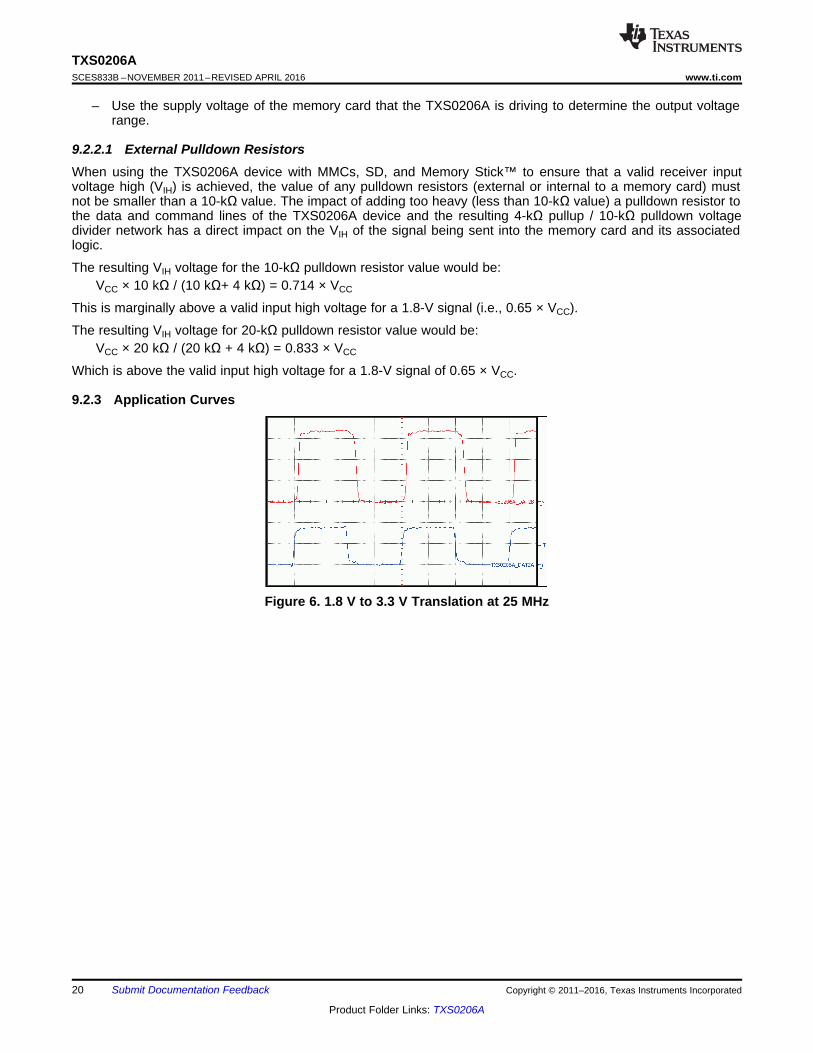
9.2.2.1 External Pulldown ResistorsWhen using the TXS0206A device with MMCs, SD, and Memory Stick™ to ensure that a valid receiver inputvoltage high (VIH) is achieved, the value of any pulldown resistors (external or internal to a memory card) mustnot be smaller than a 10-kΩ value. The impact of adding too heavy (less than 10-kΩ value) a pulldown resistor tothe data and command lines of the TXS0206A device and the resulting 4-kΩ pullup / 10-kΩ pulldown voltagedivider network has a direct impact on the VIH of the signal being sent into the memory card and its associatedlogic.
The resulting VIH voltage for the 10-kΩ pulldown resistor value would be:VCC × 10 kΩ / (10 kΩ+ 4 kΩ) = 0.714 × VCC
This is marginally above a valid input high voltage for a 1.8-V signal (i.e., 0.65 × VCC).
The resulting VIH voltage for 20-kΩ pulldown resistor value would be:VCC × 20 kΩ / (20 kΩ + 4 kΩ) = 0.833 × VCC
Which is above the valid input high voltage for a 1.8-V signal of 0.65 × VCC.
9.2.3 Application Curves
Figure 6. 1.8 V to 3.3 V Translation at 25 MHz

E4
A4
B4
D4
DAT1B
DAT2B
DAT3BDAT0B
DAT1B
CLKB
CMDB
CLKB
DAT0B
0
1
2
3
4
5
6
7
8
10
11
12
VCCA
DAT0A
DAT1A
DAT2A
DAT3A
CMDA
CLKA
CLK-f
GND
GND
VCCB
DAT0B
DAT1B
DAT2B
DAT3B
CMDB
CLKB
VDDA
DAT0
DAT1
DAT2
DAT3
CMD
CLK
CLKin
GND
CD
DAT2
DAT3
CMD
VSS1
VDD
CLK
VSS2
DAT0
DAT1
CD (Physical)
GND
GND
A2
D1
E1
A1
B1
C1
D2
E2
C2
C3
VCCA VCCB
Processor
SD/SDIO MMC
TXS0206A
C30.1 µF
C40.1 µF
C10.1 µF
VCCB
U1A U2 J1
DAT2B
DAT3B
CMDB
B3
C4
D3CD
Standard SD Card
CDCD
B214 WP (Physical)
VCCA
WP
E4
A4
B4
D4
DAT1B
DAT2B
DAT3BDAT0B
DAT1B
CLKB
CMDB
CLKB
DAT0B
0
1
2
3
4
5
6
7
8
10
11
12
VCCA
DAT0A
DAT1A
DAT2A
DAT3A
CMDA
CLKA
CLK-f
GND
GND
VCCB
DAT0B
DAT1B
DAT2B
DAT3B
CMDB
CLKB
VDDA
DAT0
DAT1
DAT2
DAT3
CMD
CLK
CLKin
GND
CD
DAT2
DAT3
CMD
VSS1
VDD
CLK
VSS2
DAT0
DAT1
CD (Physical)
GND
GND
A2
D1
E1
A1
B1
C1
D2
E2
C2
C3
VCCA VCCB
Processor
SD/SDIO MMC
TXS0206A
C30.1 µF
C40.1 µF
C10.1 µF
VCCB
U1A U2 J1
DAT2B
DAT3B
CMDB
B3
C4
D3CD
54794-0978Micro SD
CDCD
B2
21
TXS0206Awww.ti.com SCES833B –NOVEMBER 2011–REVISED APRIL 2016
Product Folder Links: TXS0206A
Submit Documentation FeedbackCopyright © 2011–2016, Texas Instruments Incorporated
9.3 System Examples
Figure 7. Interfacing With SD/SDIO Card
Figure 8. Interfacing With Seperate WP and CD Pin

E4
A4
B4
D4
DAT1B
DAT2B
DAT3B
CMDB
CMDB
CLKB
DAT0B
VCCA
DAT0A
DAT1A
DAT2A
DAT3A
CMDA
CLKA
CLK-f
GND
GND
VCCB
DAT0B
DAT1B
DAT2BDAT3B
CMDB
CLKB
VDDA
DAT0
DAT1
DAT2
DAT3
CMD
CLK
CLKin
GND
CDVSS
A2
D1
E1
A1
B1
C1
D2
E2
C2
C3
VCCA VCCB
Memory Stick
Controller
™ TXS0206
C3
0.1 µF
C4
0.1 µF
C1
0.1 µF
VCCB
U1A U2
B3
C4
D3
Memory Stick™
Connector
CDCD
B2VCC
SCLK
DATA3 (see Note)
INS
DATA2 (see Note)
DATA0/SDIO (see Note)
DATA1 (see Note)
BS
VSS1
DAT1B
2
DAT0B
3
DAT2B
4
CD
5
DAT3B
6
CLKB
7
8
9
10
22
TXS0206ASCES833B –NOVEMBER 2011–REVISED APRIL 2016 www.ti.com
Product Folder Links: TXS0206A
Submit Documentation Feedback Copyright © 2011–2016, Texas Instruments Incorporated
System Examples (continued)
Figure 9. Interfacing With Memory Stick™ Card
10 Power Supply RecommendationsThe TXS0206A does not require power sequencing between VCCA and VCCB during power-up so the power-supply rails can be ramped in any order.
The EN pin is referenced to VCCA and when configured to low, will place all outputs into a high-impedance state.To ensure the high-impedance state of the outputs during power up or power down, the EN pin must be tied toGND through a pulldown resistor and must not be enabled until VCCA and VCCB are fully ramped and stable. Theminimum value of the pulldown resistor to ground is determined by the current-sourcing capability of the drivercontrolling the EN pin.
Finally, the EN pin may be shorted to VCCA if the application does not require use of the high-impedance state atany time.
11 Layout
11.1 Layout GuidelinesTo ensure reliability of the device, TI recommends following common printed-circuit board layout guidelines.• Bypass capacitors should be used on power supplies.• Short trace lengths should be used to avoid excessive loading• PCB signal trace-lengths must be kept short enough so that the round-trip delay of any reflection is less than
the one shot duration, approximately 30 ns, ensuring that any reflection encounters low impedance at thesource driver
• With very heavy capacitive loads, the one-shot can time-out before the signal is driven fully to the positive rail,so it is recommended that this lumped-load capacitance be considered and kept below 50 pF to avoid O.S.retriggering, bus contention, output signal oscillations, or other adverse system-level affects.

A
B
C
D
E
1 2 3 4
VIA to Power Plane (Inner Layer)
VIA to GND Plane (Inner Layer)
Polygonal Copper Pour
VIA to Top Layer
TXS0206AYFP(Top View)
To Connector
To Memory CardTo Host
A
B
C
D
E
1 2 3 4
1 PF
VIA to Power Plane (Inner Layer)
VIA to GND Plane (Inner Layer)
Polygonal Copper Pour
VIA to Bottom Layer
To Host
To Host
To Host
TXS0206AYFP(Top View)
To Host
To Host
To Memory Card
To Memory Card
To Memory Card
To Memory Card
To Memory Card
To Host
To Host
To Connector
23
TXS0206Awww.ti.com SCES833B –NOVEMBER 2011–REVISED APRIL 2016
Product Folder Links: TXS0206A
Submit Documentation FeedbackCopyright © 2011–2016, Texas Instruments Incorporated
11.2 Layout Example
Figure 10. TXS0206A Example Layout (Top Layer)
Figure 11. TXS0206A Example Layout (Bottom Layer)

24
TXS0206ASCES833B –NOVEMBER 2011–REVISED APRIL 2016 www.ti.com
Product Folder Links: TXS0206A
Submit Documentation Feedback Copyright © 2011–2016, Texas Instruments Incorporated
12 Device and Documentation Support
12.1 Documentation Support
12.1.1 Related DocumentationFor related documentation see the following:
• Introduction to Logic, SLVA700.• TXS0206A Evaluation Module, SCEU008.
12.2 Community ResourcesThe following links connect to TI community resources. Linked contents are provided "AS IS" by the respectivecontributors. They do not constitute TI specifications and do not necessarily reflect TI's views; see TI's Terms ofUse.
TI E2E™ Online Community TI's Engineer-to-Engineer (E2E) Community. Created to foster collaborationamong engineers. At e2e.ti.com, you can ask questions, share knowledge, explore ideas and helpsolve problems with fellow engineers.
Design Support TI's Design Support Quickly find helpful E2E forums along with design support tools andcontact information for technical support.
12.3 TrademarksE2E is a trademark of Texas Instruments.All other trademarks are the property of their respective owners.
12.4 Electrostatic Discharge CautionThese devices have limited built-in ESD protection. The leads should be shorted together or the device placed in conductive foamduring storage or handling to prevent electrostatic damage to the MOS gates.
12.5 GlossarySLYZ022 — TI Glossary.
This glossary lists and explains terms, acronyms, and definitions.
13 Mechanical, Packaging, and Orderable InformationThe following pages include mechanical, packaging, and orderable information. This information is the mostcurrent data available for the designated devices. This data is subject to change without notice and revision ofthis document. For browser-based versions of this data sheet, refer to the left-hand navigation.

PACKAGE OPTION ADDENDUM
www.ti.com 20-Jan-2016
Addendum-Page 1
PACKAGING INFORMATION
Orderable Device Status(1)
Package Type PackageDrawing
Pins PackageQty
Eco Plan(2)
Lead/Ball Finish(6)
MSL Peak Temp(3)
Op Temp (°C) Device Marking(4/5)
Samples
TXS0206AYFPR ACTIVE DSBGA YFP 20 3000 Green (RoHS& no Sb/Br)
SNAGCU Level-1-260C-UNLIM -40 to 85 TXS0206A
(1) The marketing status values are defined as follows:ACTIVE: Product device recommended for new designs.LIFEBUY: TI has announced that the device will be discontinued, and a lifetime-buy period is in effect.NRND: Not recommended for new designs. Device is in production to support existing customers, but TI does not recommend using this part in a new design.PREVIEW: Device has been announced but is not in production. Samples may or may not be available.OBSOLETE: TI has discontinued the production of the device.
(2) Eco Plan - The planned eco-friendly classification: Pb-Free (RoHS), Pb-Free (RoHS Exempt), or Green (RoHS & no Sb/Br) - please check http://www.ti.com/productcontent for the latest availabilityinformation and additional product content details.TBD: The Pb-Free/Green conversion plan has not been defined.Pb-Free (RoHS): TI's terms "Lead-Free" or "Pb-Free" mean semiconductor products that are compatible with the current RoHS requirements for all 6 substances, including the requirement thatlead not exceed 0.1% by weight in homogeneous materials. Where designed to be soldered at high temperatures, TI Pb-Free products are suitable for use in specified lead-free processes.Pb-Free (RoHS Exempt): This component has a RoHS exemption for either 1) lead-based flip-chip solder bumps used between the die and package, or 2) lead-based die adhesive used betweenthe die and leadframe. The component is otherwise considered Pb-Free (RoHS compatible) as defined above.Green (RoHS & no Sb/Br): TI defines "Green" to mean Pb-Free (RoHS compatible), and free of Bromine (Br) and Antimony (Sb) based flame retardants (Br or Sb do not exceed 0.1% by weightin homogeneous material)
(3) MSL, Peak Temp. - The Moisture Sensitivity Level rating according to the JEDEC industry standard classifications, and peak solder temperature.
(4) There may be additional marking, which relates to the logo, the lot trace code information, or the environmental category on the device.
(5) Multiple Device Markings will be inside parentheses. Only one Device Marking contained in parentheses and separated by a "~" will appear on a device. If a line is indented then it is a continuationof the previous line and the two combined represent the entire Device Marking for that device.
(6) Lead/Ball Finish - Orderable Devices may have multiple material finish options. Finish options are separated by a vertical ruled line. Lead/Ball Finish values may wrap to two lines if the finishvalue exceeds the maximum column width.
Important Information and Disclaimer:The information provided on this page represents TI's knowledge and belief as of the date that it is provided. TI bases its knowledge and belief on informationprovided by third parties, and makes no representation or warranty as to the accuracy of such information. Efforts are underway to better integrate information from third parties. TI has taken andcontinues to take reasonable steps to provide representative and accurate information but may not have conducted destructive testing or chemical analysis on incoming materials and chemicals.TI and TI suppliers consider certain information to be proprietary, and thus CAS numbers and other limited information may not be available for release.
In no event shall TI's liability arising out of such information exceed the total purchase price of the TI part(s) at issue in this document sold by TI to Customer on an annual basis.

PACKAGE OPTION ADDENDUM
www.ti.com 20-Jan-2016
Addendum-Page 2

TAPE AND REEL INFORMATION
*All dimensions are nominal
Device PackageType
PackageDrawing
Pins SPQ ReelDiameter
(mm)
ReelWidth
W1 (mm)
A0(mm)
B0(mm)
K0(mm)
P1(mm)
W(mm)
Pin1Quadrant
TXS0206AYFPR DSBGA YFP 20 3000 180.0 8.4 1.66 2.06 0.56 4.0 8.0 Q1
PACKAGE MATERIALS INFORMATION
www.ti.com 20-Jan-2016
Pack Materials-Page 1
*All dimensions are nominal
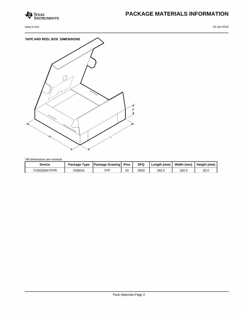
Device Package Type Package Drawing Pins SPQ Length (mm) Width (mm) Height (mm)
TXS0206AYFPR DSBGA YFP 20 3000 182.0 182.0 20.0
PACKAGE MATERIALS INFORMATION
www.ti.com 20-Jan-2016
Pack Materials-Page 2

www.ti.com
PACKAGE OUTLINE
C0.5 MAX
0.190.13
1.6TYP
1.2 TYP
0.4 TYP
0.4 TYP20X 0.25
0.21
B E A
D
4222895/A 04/2016
DSBGA - 0.5 mm max heightYFP0020DIE SIZE BALL GRID ARRAY
NOTES: 1. All linear dimensions are in millimeters. Any dimensions in parenthesis are for reference only. Dimensioning and tolerancing per ASME Y14.5M.2. This drawing is subject to change without notice.
BALL A1CORNER
SEATING PLANE
BALL TYP 0.05 C
A
B
C
D
1 2 3
0.015 C A B
E
4
SYMM
SYMM
SCALE 7.000
D: Max =
E: Max =
1.988 mm, Min =
1.588 mm, Min =
1.928 mm
1.527 mm

www.ti.com
EXAMPLE BOARD LAYOUT
20X ( )0.23
(0.4) TYP
(0.4) TYP
( )METAL
0.23 0.05 MAX
SOLDER MASKOPENING
METAL UNDERSOLDER MASK
( )SOLDER MASKOPENING
0.23
0.05 MIN
4222895/A 04/2016
DSBGA - 0.5 mm max heightYFP0020DIE SIZE BALL GRID ARRAY
NOTES: (continued) 3. Final dimensions may vary due to manufacturing tolerance considerations and also routing constraints. For more information, see Texas Instruments literature number SNVA009 (www.ti.com/lit/snva009).
SOLDER MASK DETAILSNOT TO SCALE
SYMM
SYMM
LAND PATTERN EXAMPLESCALE:25X
A
B
C
D
1 2 3 4
E
NON-SOLDER MASKDEFINED
(PREFERRED)
SOLDER MASKDEFINED

www.ti.com
EXAMPLE STENCIL DESIGN
(0.4) TYP
(0.4) TYP
20X ( 0.25) (R ) TYP0.05
METALTYP
4222895/A 04/2016
DSBGA - 0.5 mm max heightYFP0020DIE SIZE BALL GRID ARRAY
NOTES: (continued) 4. Laser cutting apertures with trapezoidal walls and rounded corners may offer better paste release.
SYMM
SYMM
SOLDER PASTE EXAMPLEBASED ON 0.1 mm THICK STENCIL
SCALE:30X
A
B
C
D
1 2 3
E
4

IMPORTANT NOTICE
Texas Instruments Incorporated (TI) reserves the right to make corrections, enhancements, improvements and other changes to itssemiconductor products and services per JESD46, latest issue, and to discontinue any product or service per JESD48, latest issue. Buyersshould obtain the latest relevant information before placing orders and should verify that such information is current and complete.TI’s published terms of sale for semiconductor products (http://www.ti.com/sc/docs/stdterms.htm) apply to the sale of packaged integratedcircuit products that TI has qualified and released to market. Additional terms may apply to the use or sale of other types of TI products andservices.Reproduction of significant portions of TI information in TI data sheets is permissible only if reproduction is without alteration and isaccompanied by all associated warranties, conditions, limitations, and notices. TI is not responsible or liable for such reproduceddocumentation. Information of third parties may be subject to additional restrictions. Resale of TI products or services with statementsdifferent from or beyond the parameters stated by TI for that product or service voids all express and any implied warranties for theassociated TI product or service and is an unfair and deceptive business practice. TI is not responsible or liable for any such statements.Buyers and others who are developing systems that incorporate TI products (collectively, “Designers”) understand and agree that Designersremain responsible for using their independent analysis, evaluation and judgment in designing their applications and that Designers havefull and exclusive responsibility to assure the safety of Designers' applications and compliance of their applications (and of all TI productsused in or for Designers’ applications) with all applicable regulations, laws and other applicable requirements. Designer represents that, withrespect to their applications, Designer has all the necessary expertise to create and implement safeguards that (1) anticipate dangerousconsequences of failures, (2) monitor failures and their consequences, and (3) lessen the likelihood of failures that might cause harm andtake appropriate actions. Designer agrees that prior to using or distributing any applications that include TI products, Designer willthoroughly test such applications and the functionality of such TI products as used in such applications.TI’s provision of technical, application or other design advice, quality characterization, reliability data or other services or information,including, but not limited to, reference designs and materials relating to evaluation modules, (collectively, “TI Resources”) are intended toassist designers who are developing applications that incorporate TI products; by downloading, accessing or using TI Resources in anyway, Designer (individually or, if Designer is acting on behalf of a company, Designer’s company) agrees to use any particular TI Resourcesolely for this purpose and subject to the terms of this Notice.TI’s provision of TI Resources does not expand or otherwise alter TI’s applicable published warranties or warranty disclaimers for TIproducts, and no additional obligations or liabilities arise from TI providing such TI Resources. TI reserves the right to make corrections,enhancements, improvements and other changes to its TI Resources. TI has not conducted any testing other than that specificallydescribed in the published documentation for a particular TI Resource.Designer is authorized to use, copy and modify any individual TI Resource only in connection with the development of applications thatinclude the TI product(s) identified in such TI Resource. NO OTHER LICENSE, EXPRESS OR IMPLIED, BY ESTOPPEL OR OTHERWISETO ANY OTHER TI INTELLECTUAL PROPERTY RIGHT, AND NO LICENSE TO ANY TECHNOLOGY OR INTELLECTUAL PROPERTYRIGHT OF TI OR ANY THIRD PARTY IS GRANTED HEREIN, including but not limited to any patent right, copyright, mask work right, orother intellectual property right relating to any combination, machine, or process in which TI products or services are used. Informationregarding or referencing third-party products or services does not constitute a license to use such products or services, or a warranty orendorsement thereof. Use of TI Resources may require a license from a third party under the patents or other intellectual property of thethird party, or a license from TI under the patents or other intellectual property of TI.TI RESOURCES ARE PROVIDED “AS IS” AND WITH ALL FAULTS. TI DISCLAIMS ALL OTHER WARRANTIES ORREPRESENTATIONS, EXPRESS OR IMPLIED, REGARDING RESOURCES OR USE THEREOF, INCLUDING BUT NOT LIMITED TOACCURACY OR COMPLETENESS, TITLE, ANY EPIDEMIC FAILURE WARRANTY AND ANY IMPLIED WARRANTIES OFMERCHANTABILITY, FITNESS FOR A PARTICULAR PURPOSE, AND NON-INFRINGEMENT OF ANY THIRD PARTY INTELLECTUALPROPERTY RIGHTS. TI SHALL NOT BE LIABLE FOR AND SHALL NOT DEFEND OR INDEMNIFY DESIGNER AGAINST ANY CLAIM,INCLUDING BUT NOT LIMITED TO ANY INFRINGEMENT CLAIM THAT RELATES TO OR IS BASED ON ANY COMBINATION OFPRODUCTS EVEN IF DESCRIBED IN TI RESOURCES OR OTHERWISE. IN NO EVENT SHALL TI BE LIABLE FOR ANY ACTUAL,DIRECT, SPECIAL, COLLATERAL, INDIRECT, PUNITIVE, INCIDENTAL, CONSEQUENTIAL OR EXEMPLARY DAMAGES INCONNECTION WITH OR ARISING OUT OF TI RESOURCES OR USE THEREOF, AND REGARDLESS OF WHETHER TI HAS BEENADVISED OF THE POSSIBILITY OF SUCH DAMAGES.Unless TI has explicitly designated an individual product as meeting the requirements of a particular industry standard (e.g., ISO/TS 16949and ISO 26262), TI is not responsible for any failure to meet such industry standard requirements.Where TI specifically promotes products as facilitating functional safety or as compliant with industry functional safety standards, suchproducts are intended to help enable customers to design and create their own applications that meet applicable functional safety standardsand requirements. Using products in an application does not by itself establish any safety features in the application. Designers mustensure compliance with safety-related requirements and standards applicable to their applications. Designer may not use any TI products inlife-critical medical equipment unless authorized officers of the parties have executed a special contract specifically governing such use.Life-critical medical equipment is medical equipment where failure of such equipment would cause serious bodily injury or death (e.g., lifesupport, pacemakers, defibrillators, heart pumps, neurostimulators, and implantables). Such equipment includes, without limitation, allmedical devices identified by the U.S. Food and Drug Administration as Class III devices and equivalent classifications outside the U.S.TI may expressly designate certain products as completing a particular qualification (e.g., Q100, Military Grade, or Enhanced Product).Designers agree that it has the necessary expertise to select the product with the appropriate qualification designation for their applicationsand that proper product selection is at Designers’ own risk. Designers are solely responsible for compliance with all legal and regulatoryrequirements in connection with such selection.Designer will fully indemnify TI and its representatives against any damages, costs, losses, and/or liabilities arising out of Designer’s non-compliance with the terms and provisions of this Notice.
Mailing Address: Texas Instruments, Post Office Box 655303, Dallas, Texas 75265Copyright © 2017, Texas Instruments Incorporated