Titelmasterformat durch Klicken bearbeiten · • DC-DC • Inductors, chokes, transformers •...
28
© CADFEM 2017 Simulationsgestützte Entwicklung Leistungselektronischer Schaltungslayouts Auswirkungen parasitärer RLC auf das Schaltverhalten verstehen und optimieren 1
Transcript of Titelmasterformat durch Klicken bearbeiten · • DC-DC • Inductors, chokes, transformers •...

Titelmasterformat durch Klicken bearbeiten
© CADFEM 2017
Simulationsgestützte Entwicklung
Leistungselektronischer Schaltungslayouts
Auswirkungen parasitärer RLC auf das Schaltverhalten verstehen und
optimieren
1

© CADFEM 2017
Power Electronics as Enabler for an Energy Efficient World
3
Image Source: Freeimages.com

© CADFEM 2017
New Challenges in Hardware Development for Power Electronics
4
High
power
Increased
switching
frequencies
High
efficiency
Steep
switching
edges
Thermal
management
EMICircuit
layout
parasitics
Compact
layout
Eddy effects
in inductors
3D Physics
Effects!
3D Physics
Effects!
3D Physics
Effects!
Wide
Bandgap
Devices
© CADFEM 2017
Hardware Development for Power Electronics
5
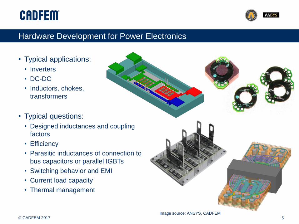
• Typical applications:
• Inverters
• DC-DC
• Inductors, chokes,
transformers
• Typical questions:
• Designed inductances and coupling
factors
• Efficiency
• Parasitic inductances of connection to
bus capacitors or parallel IGBTs
• Switching behavior and EMI
• Current load capacity
• Thermal management
Image source: ANSYS, CADFEM
© CADFEM 2017
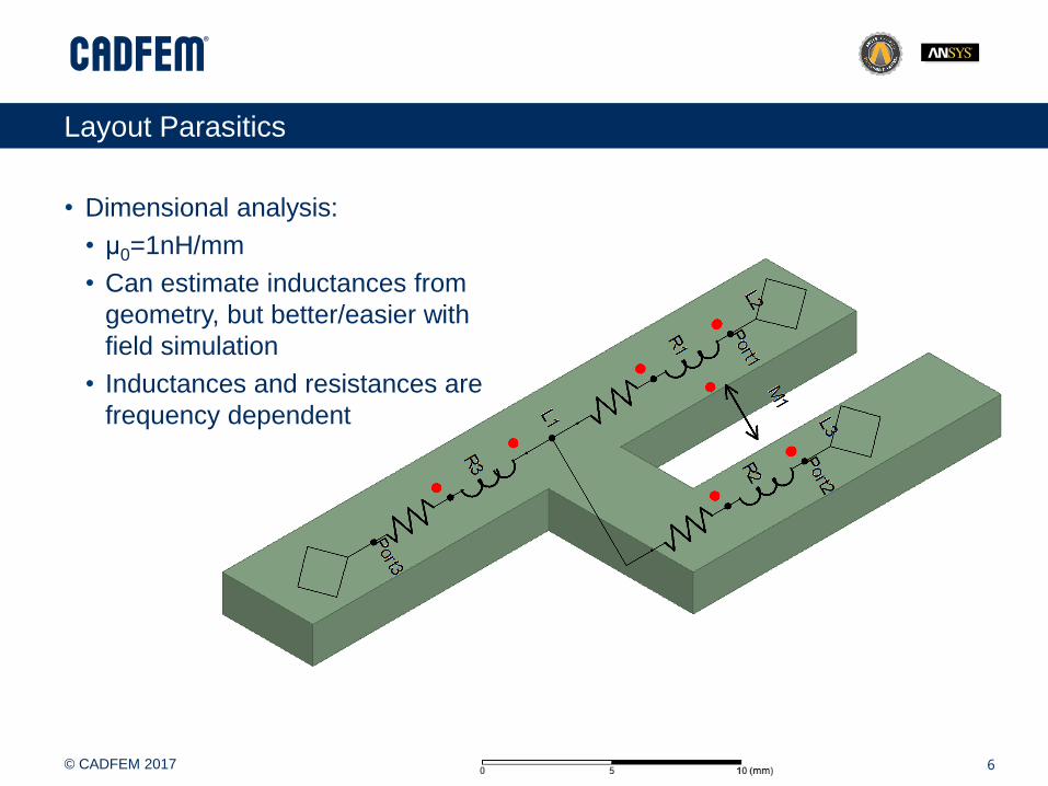
Layout Parasitics
6
• Dimensional analysis:
• μ0=1nH/mm
• Can estimate inductances from
geometry, but better/easier with
field simulation
• Inductances and resistances are
frequency dependent
© CADFEM 2017
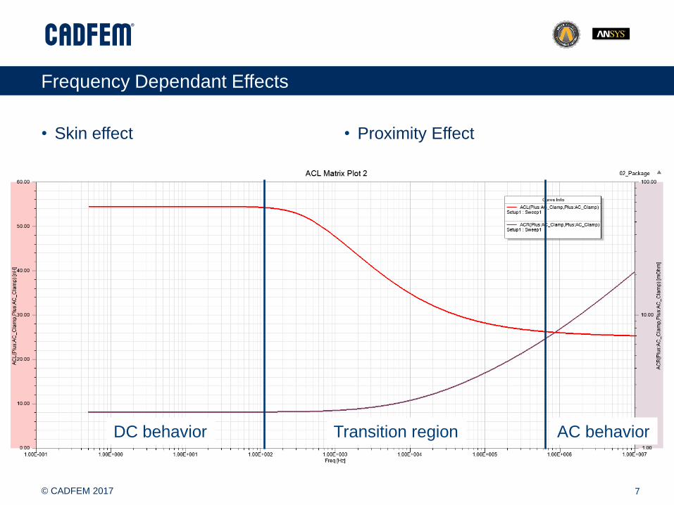
Frequency Dependant Effects
7
• Skin effect • Proximity Effect
DC behavior AC behaviorTransition region

© CADFEM 2017
Layout Parasitics
8
• Dimensional analysis:
• ε0=9pF/m
• Can estimate capacitances from
geometry, but better/easier with
field simulation
© CADFEM 2017
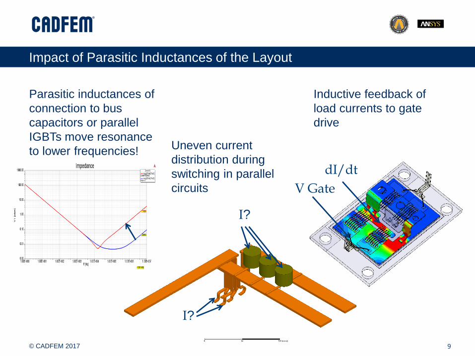
Impact of Parasitic Inductances of the Layout
9
Parasitic inductances of
connection to bus
capacitors or parallel
IGBTs move resonance
to lower frequencies!
Inductive feedback of
load currents to gate
drive
Uneven current
distribution during
switching in parallel
circuits
I?
I?
V Gate
dI/dt

© CADFEM 2017
Simulationsgestützte Entwicklung
10
Konzeptphase
Detaillierung Produktion
Evaluierung/
Versuchsphase
Vorbereitung
Produktion
Kosten für
Änderungen
Kosten für
Änderungen
Kosten für
Änderungen
Finales Design
# Ä
nderu
ngen Simulationsgestützte
Entwicklung
„Das Produkt verstehen, weiterentwickeln
und optimieren bevor es gebaut wird.“
© CADFEM 2017
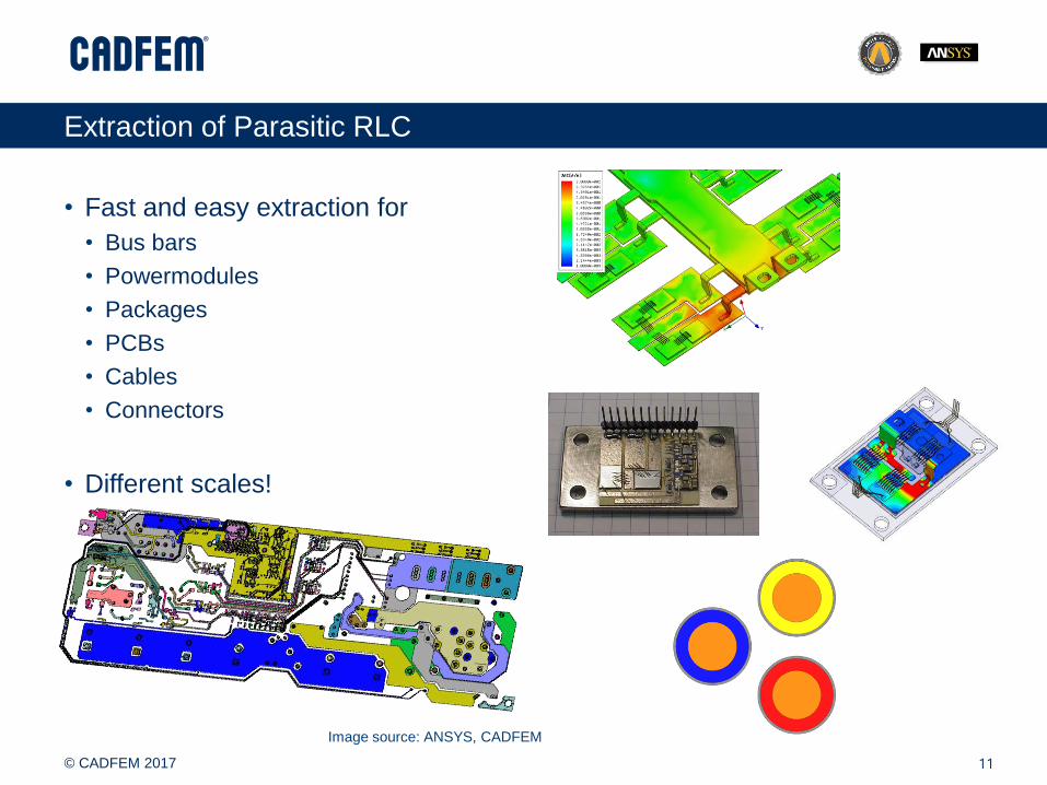
Extraction of Parasitic RLC
11
• Fast and easy extraction for
• Bus bars
• Powermodules
• Packages
• PCBs
• Cables
• Connectors
• Different scales!
Image source: ANSYS, CADFEM
© CADFEM 2017
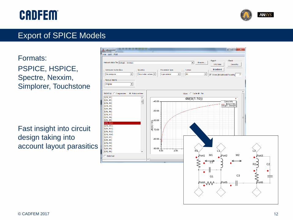
Export of SPICE Models
12
Formats:
PSPICE, HSPICE,
Spectre, Nexxim,
Simplorer, Touchstone
Fast insight into circuit
design taking into
account layout parasiticsR1 L1
C1
G1
M1 M2
L2
R2
Port1 Port2 Port3
Port4 Port5 Port6
C2
C3
Titelmasterformat durch Klicken bearbeiten
© CADFEM 2017
Impact of Parasitics on the Performance of
Inverters
13
© CADFEM 2017
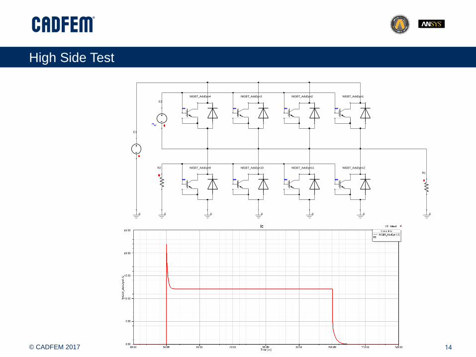
High Side Test
14
0 0 0 0 00 0
E1
NIGBT_AdvDyn1
E2
R1
R2
NIGBT_AdvDyn2NIGBT_AdvDyn3NIGBT_AdvDyn4
NIGBT_AdvDyn9 NIGBT_AdvDyn10 NIGBT_AdvDyn11 NIGBT_AdvDyn12
© CADFEM 2017
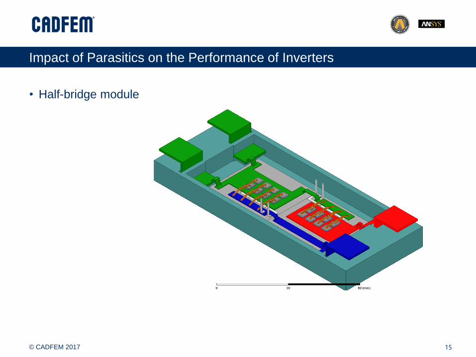
Impact of Parasitics on the Performance of Inverters
15
• Half-bridge module
© CADFEM 2017
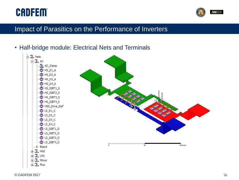
Impact of Parasitics on the Performance of Inverters
16
• Half-bridge module: Electrical Nets and Terminals
© CADFEM 2017
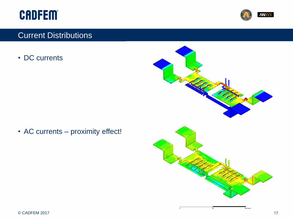
Current Distributions
17
• DC currents
• AC currents – proximity effect!

© CADFEM 2017
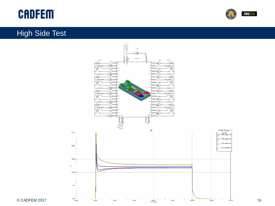
High Side Test
18
0 0 0 0 00 0
E1
NIGBT_AdvDyn1
E2
R1
R2
NIGBT_AdvDyn2NIGBT_AdvDyn3NIGBT_AdvDyn4
NIGBT_AdvDyn9 NIGBT_AdvDyn10 NIGBT_AdvDyn11 NIGBT_AdvDyn12
© CADFEM 2017
High Side Test
19
0
E1
NIGBT_AdvDyn1
NIGBT_AdvDyn2
NIGBT_AdvDyn3
NIGBT_AdvDyn4
NIGBT_AdvDyn5
NIGBT_AdvDyn6
NIGBT_AdvDyn7
NIGBT_AdvDyn8
Diode60_1
Diode60_2
Diode60_3
Diode60_4
Diode60_5
Diode60_6
Diode60_7
Diode60_8
E2
R1
R2
AC_HS_D1_A
AC_HS_D2_A
AC_HS_D3_A
AC_HS_D4_A
AC_HS_IGBT1_S
AC_HS_IGBT2_S
AC_HS_IGBT3_S
AC_HS_IGBT4_S
AC
_H
SG
_D
riv
e_
Re
f
AC_LS_D1_C
AC_LS_D2_C
AC_LS_D3_C
AC_LS_D4_C
AC_LS_IGBT1_D
AC_LS_IGBT2_D
AC_LS_IGBT3_D
AC_LS_IGBT4_D
HSG_HS_IGBT1_G
HSG_HS_IGBT2_G
HSG_HS_IGBT3_G
HSG_HS_IGBT4_G
LSG_LS_IGBT1_G
LSG_LS_IGBT2_G
LSG_LS_IGBT3_G
LSG_LS_IGBT4_G
Minus_LS_D1_A
Minus_LS_D2_A
Minus_LS_D3_A
Minus_LS_D4_A
Minus_LS_IGBT1_S
Minus_LS_IGBT2_S
Minus_LS_IGBT3_S
Minus_LS_IGBT4_S
Min
us
_L
SG
_D
riv
e_
Re
f
Plus_HS_D1_C
Plus_HS_D2_C
Plus_HS_D3_C
Plus_HS_D4_C
Plus_HS_IGBT1_D
Plus_HS_IGBT2_D
Plus_HS_IGBT3_D
Plus_HS_IGBT4_D
AC
_A
C_
Cla
mp
HS
G_
HS
G_
Dri
ve
LS
G_
LS
G_
Dri
ve
Min
us
_M
inu
s_
Cla
mp
Plu
s_
Plu
s_
Cla
mp
package_sp1
A
AM1
A
AM2
A
AM3
A
AM4
A
AM5
A
AM6
A
AM7
A
AM8
A
AM9
A
AM10
A
AM11
A
AM12
A
AM13
A
AM14
A
AM15
A
AM16
A
AM17
A
AM18

© CADFEM 2017
Transient Simulation of Signales
20
• Switching edges
• Short circuit
• Conducted emissions
0
E1
NIGBT_AdvDyn1
NIGBT_AdvDyn2
NIGBT_AdvDyn3
NIGBT_AdvDyn4
NIGBT_AdvDyn5
NIGBT_AdvDyn6
NIGBT_AdvDyn7
NIGBT_AdvDyn8
Diode60_1
Diode60_2
Diode60_3
Diode60_4
Diode60_5
Diode60_6
Diode60_7
Diode60_8
E2
R1
R2
AC_HS_D1_A
AC_HS_D2_A
AC_HS_D3_A
AC_HS_D4_A
AC_HS_IGBT1_S
AC_HS_IGBT2_S
AC_HS_IGBT3_S
AC_HS_IGBT4_S
AC
_H
SG
_D
riv
e_
Re
f
AC_LS_D1_C
AC_LS_D2_C
AC_LS_D3_C
AC_LS_D4_C
AC_LS_IGBT1_D
AC_LS_IGBT2_D
AC_LS_IGBT3_D
AC_LS_IGBT4_D
HSG_HS_IGBT1_G
HSG_HS_IGBT2_G
HSG_HS_IGBT3_G
HSG_HS_IGBT4_G
LSG_LS_IGBT1_G
LSG_LS_IGBT2_G
LSG_LS_IGBT3_G
LSG_LS_IGBT4_G
Minus_LS_D1_A
Minus_LS_D2_A
Minus_LS_D3_A
Minus_LS_D4_A
Minus_LS_IGBT1_S
Minus_LS_IGBT2_S
Minus_LS_IGBT3_S
Minus_LS_IGBT4_S
Min
us
_L
SG
_D
riv
e_
Re
f
Plus_HS_D1_C
Plus_HS_D2_C
Plus_HS_D3_C
Plus_HS_D4_C
Plus_HS_IGBT1_D
Plus_HS_IGBT2_D
Plus_HS_IGBT3_D
Plus_HS_IGBT4_D
AC
_A
C_
Cla
mp
HS
G_
HS
G_
Dri
ve
LS
G_
LS
G_
Dri
ve
Min
us
_M
inu
s_
Cla
mp
Plu
s_
Plu
s_
Cla
mp
package_sp1
A
AM1
A
AM2
A
AM3
A
AM4
A
AM5
A
AM6
A
AM7
A
AM8
A
AM9
A
AM10
A
AM11
A
AM12
A
AM13
A
AM14
A
AM15
A
AM16
A
AM17
A
AM18
Dominated by
AC inductance
Dominated by
DC resistance
Currents through HS IGBTs
Gate voltages at HS IGBTs
© CADFEM 2017
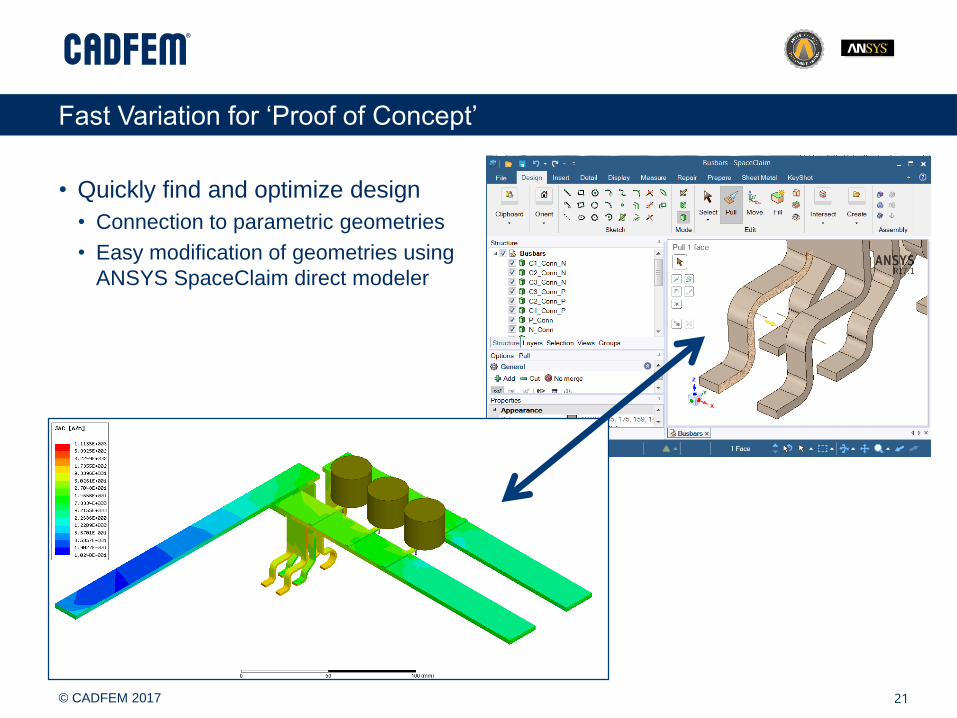
Fast Variation for ‘Proof of Concept’
21
• Quickly find and optimize design
• Connection to parametric geometries
• Easy modification of geometries using
ANSYS SpaceClaim direct modeler

Titelmasterformat durch Klicken bearbeiten
© CADFEM 2017
Conducted Emissions of a DC-DC Converter
22
© CADFEM 2017
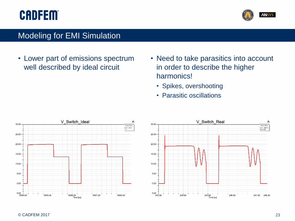
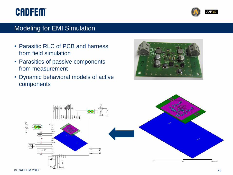
Modeling for EMI Simulation
23
• Lower part of emissions spectrum
well described by ideal circuit
• Need to take parasitics into account
in order to describe the higher
harmonics!
• Spikes, overshooting
• Parasitic oscillations
© CADFEM 2017
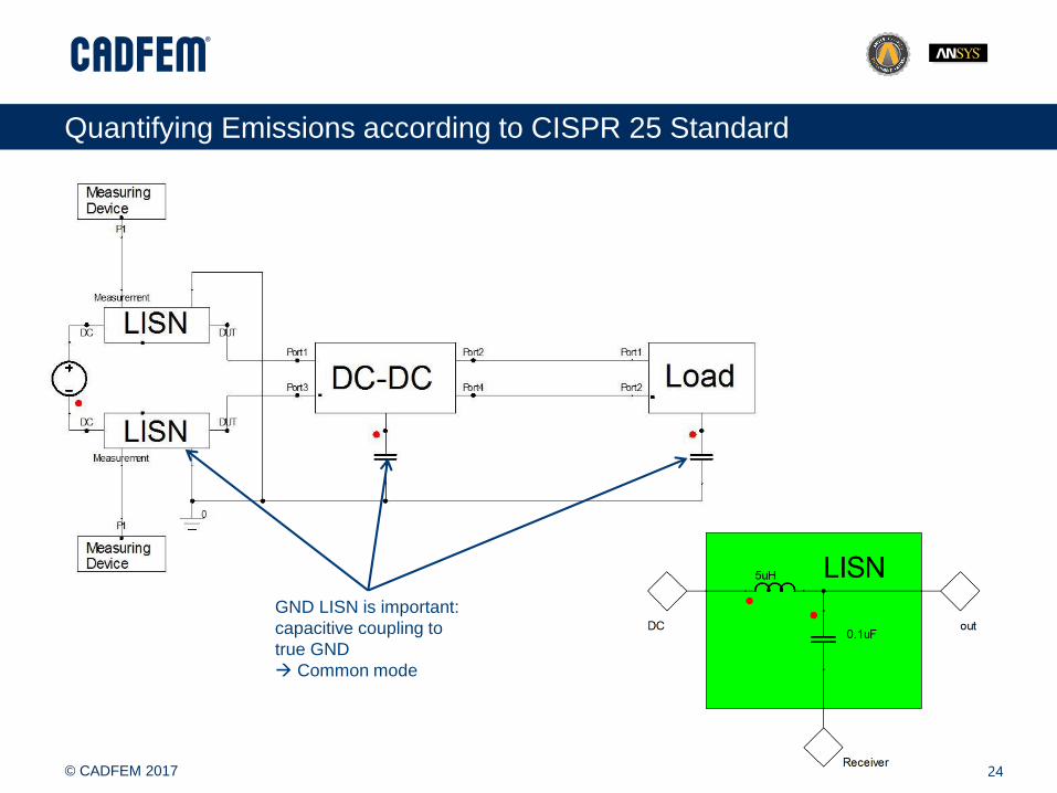
Quantifying Emissions according to CISPR 25 Standard
24
GND LISN is important:
capacitive coupling to
true GND
→ Common mode
© CADFEM 2017
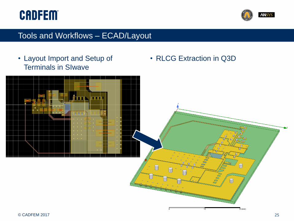
Tools and Workflows – ECAD/Layout
25
• Layout Import and Setup of
Terminals in SIwave
• RLCG Extraction in Q3D
© CADFEM 2017
Modeling for EMI Simulation
26
• Parasitic RLC of PCB and harness
from field simulation
• Parasitics of passive components
from measurement
• Dynamic behavioral models of active
components
© CADFEM 2017
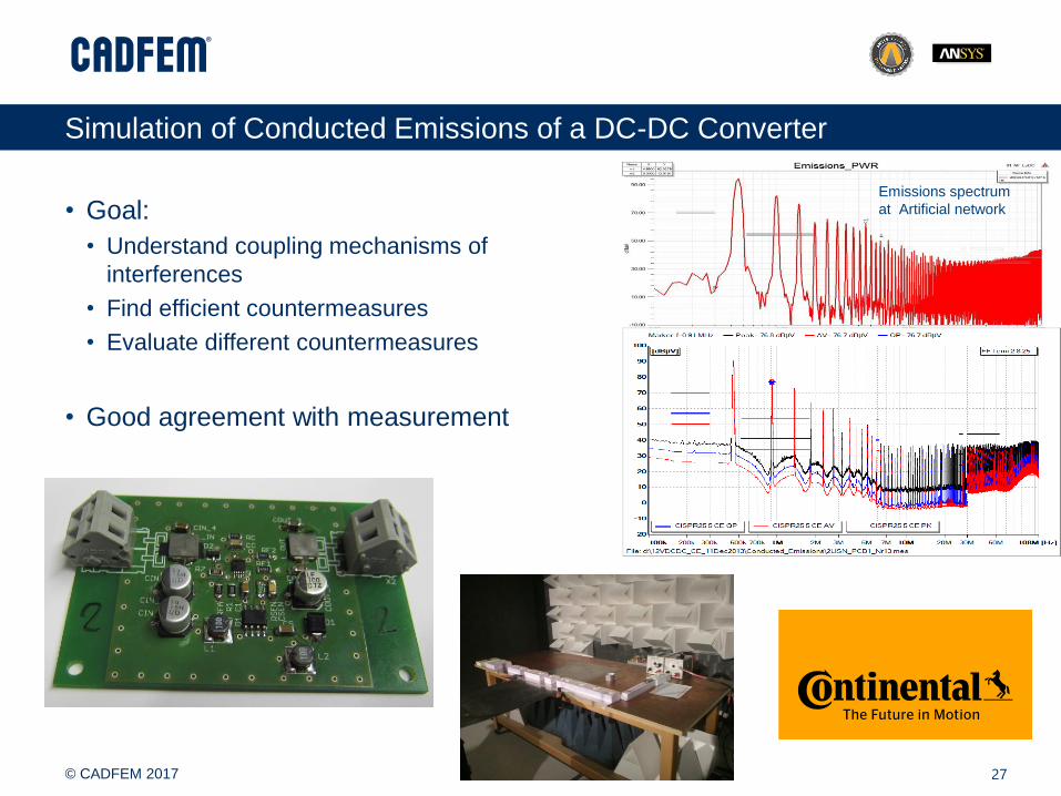
Simulation of Conducted Emissions of a DC-DC Converter
27
• Goal:
• Understand coupling mechanisms of
interferences
• Find efficient countermeasures
• Evaluate different countermeasures
• Good agreement with measurement
Emissions spectrum
at Artificial network
© CADFEM 2017
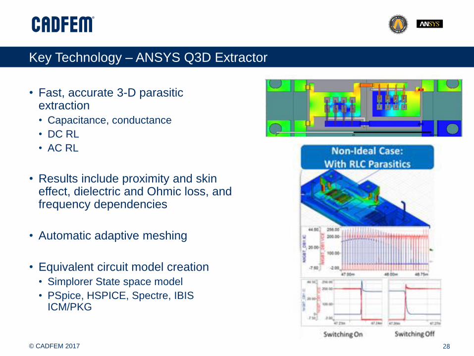
Key Technology – ANSYS Q3D Extractor
28
• Fast, accurate 3-D parasitic extraction
• Capacitance, conductance
• DC RL
• AC RL
• Results include proximity and skin effect, dielectric and Ohmic loss, and frequency dependencies
• Automatic adaptive meshing
• Equivalent circuit model creation
• Simplorer State space model
• PSpice, HSPICE, Spectre, IBIS ICM/PKG

© CADFEM 2017
CADFEM – Simulation is more than Software
29
PRODUCTS
Software und IT Solutions
SERVICES
Advice, Support, Engineering
KNOW-HOW
Transfer of knowledge
CADFEM in D, A, CH
• 1985 founded
• 2,300 customers
• 11 locations
• 220 employees (worldwide > 350)
• ANSYS Elite Channel Partner
29