THz HBTs & sub-mm-wave ICs
60
THz HBTs & sub-mm-wave ICs Mark Rodwell, UCSB Workshop: Sub-millimeter-wave Monolithic Integrated Circuits. European Microwave Week. Amsterdam, Oct. 28, 2012 [email protected] Co-Authors and Collaborators: UCSB HBT Team: J. Rode, H.W. Chiang, A. C. Gossard , B. J. Thibeault, W. Mitchell Recent Graduates: V. Jain, E. Lobisser, A. Baraskar, Teledyne HBT Team: M. Urteaga, R. Pierson, P. Rowell, B. Brar, Teledyne Scientific Company Teledyne IC Design Team: M. Seo, J. Hacker, Z. Griffith, A. Young, M. J. Choe, Teledyne Scientific Company UCSB IC Design Team: S. Danesgar, T. Reed, H-C Park, Eli Bloch
Transcript of THz HBTs & sub-mm-wave ICs

THz HBTs & sub-mm-wave ICs
Mark Rodwell, UCSB
Workshop: Sub-millimeter-wave Monolithic Integrated Circuits. European Microwave Week. Amsterdam, Oct. 28, 2012
Co-Authors and Collaborators:
UCSB HBT Team: J. Rode, H.W. Chiang, A. C. Gossard , B. J. Thibeault, W. Mitchell Recent Graduates: V. Jain, E. Lobisser, A. Baraskar,
Teledyne HBT Team: M. Urteaga, R. Pierson, P. Rowell, B. Brar, Teledyne Scientific Company
Teledyne IC Design Team: M. Seo, J. Hacker, Z. Griffith, A. Young, M. J. Choe, Teledyne Scientific Company
UCSB IC Design Team: S. Danesgar, T. Reed, H-C Park, Eli Bloch
DC to Daylight. Far-Infrared Electronics
0.1-1 THz imaging systems
109
1010
1011
1012
1013
1014
1015
Frequency (Hz)
microwave
3-30 GHz
mm-wave
30-300 GHz
far-IR
(sub-mm)
0.3-3THz
mid-IR
3-30 THz
near-IR
30-450 THz
op
tical
450
-900
TH
zHow high in frequency can we push electronics ?
...and what would be do with it ?
0.1-0.4 THz radio: vast capacity bandwidth, # channels
0.1-1 Tb/s optical fiber links

(Sub) mm-Wave Bands for Communications
very large bandwidths available
→ large transmission capacity
short wavelengths→ many parallel channels
harray widt
wavelength resolutionangular
1/2 RBN
NDB
R
22 distance)th/(wavelengarea) (aperturechannels#
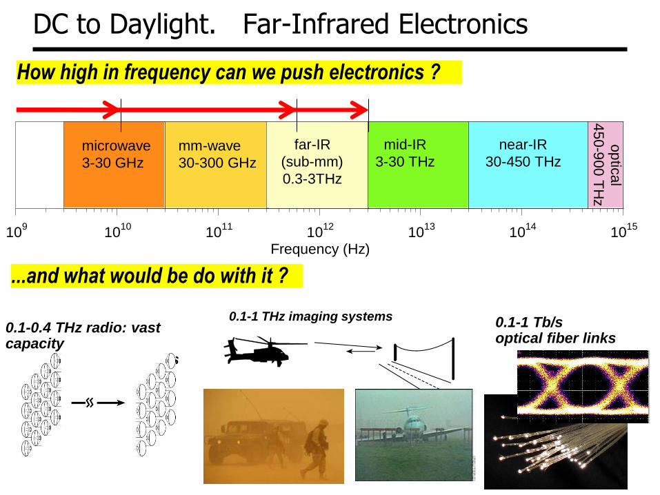
50-400 GHz Links: ~750 meters Maximum Range
rain
heavy rain
tropical deluge
Olsen, Rogers, Hodge, IEEE Trans Antennas & Propagation Mar 1978
very heavy fog
Liebe, Manabe, Hufford, IEEE Trans Antennas and Propagation, Dec. 1989
Manabe, Yoshida,
.1993 EEE Int. Conf.
on Communications,
rain 50 mm/hr: 20 dB/km, 30-1000 GHz
150 mm/hr : 50 dB/km, 30-1000 GHz
Clouds, heavy fog:
~(25 dB/km)x(frequency/500 GHz)
90% Humidity: >30 dB/km above 300 GHz
nondominant below 250 GHz (Rosker 2007 IEEE IMS)
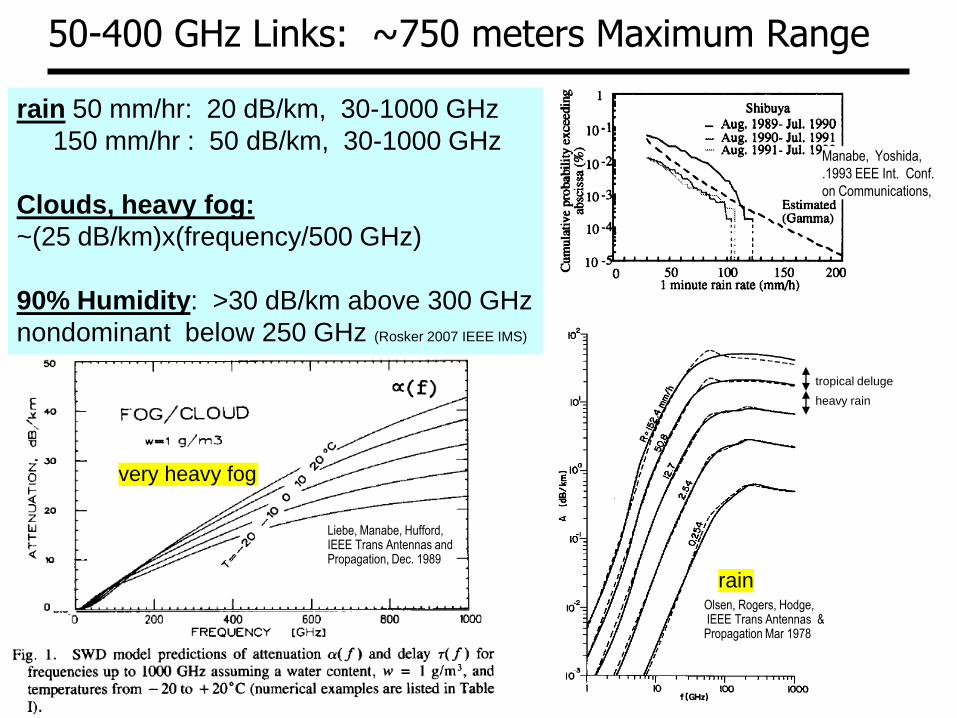
Short Wavelengths → Mesh Networks
blockedreadily Beam distancewavelength area zone Fresnel
ServiceRobust for
NetworksMesh
zone Fresnelin
blockage beam
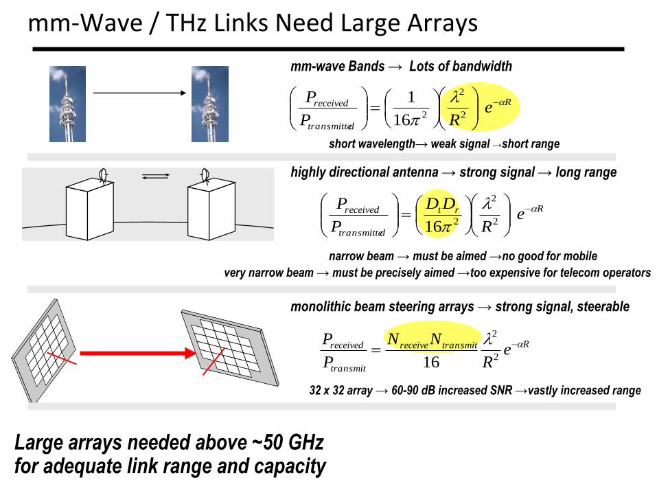
mm-Wave / THz Links Need Large Arrays
Rrt
dtransmitte
received eR
DD
P
P
16 2
2
2
R
dtransmitte
received eRP
P
16
12
2
2
mm-wave Bands → Lots of bandwidth
short wavelength→ weak signal →short range
highly directional antenna → strong signal → long range
narrow beam → must be aimed →no good for mobile
monolithic beam steering arrays → strong signal, steerable
32 x 32 array → 60-90 dB increased SNR →vastly increased range
Rtransmitreceive
transmit
received eR
NN
P
P 2
2
16
Large arrays needed above ~50 GHz for adequate link range and capacity
very narrow beam → must be precisely aimed →too expensive for telecom operators

RADAR / Imaging Needs Watts of Power, Low Noise Figure
As a function of range, weather, and data rate, effective sub-mm-wave technologies must low noise figure, high transmit power, and/or moderate to large phased arrays
220 GHz video-rate synthetic aperture radar
R
ra
image
trans eR
LHLH
RkTFf
P
2
222 4sin
4
1SNR
aircraftimagea vRf / resolution Azimuthal
ty.reflectivi 10% @
SNR dB 16
.resolution cm 5.5
image pixel 500 x 570
rate. videoHz 10
nattenuatio dB/km 7
elocityaircraft v m/s 250
elements. receive 32
aperture, totalmm 44 x mm 100
range km 1
figure. noise dB 6 power. tted W transmi50
Present 220 GHz, 66 mW PA
...to reach such levels with a solid-state source: Develop 200 mW PA 8-element array tile IC: 1.6 W
32 tiles/array→ 51 W
( 200 GHz PLL is existing design by M. Seo)
T. Reed, Z. Griffith
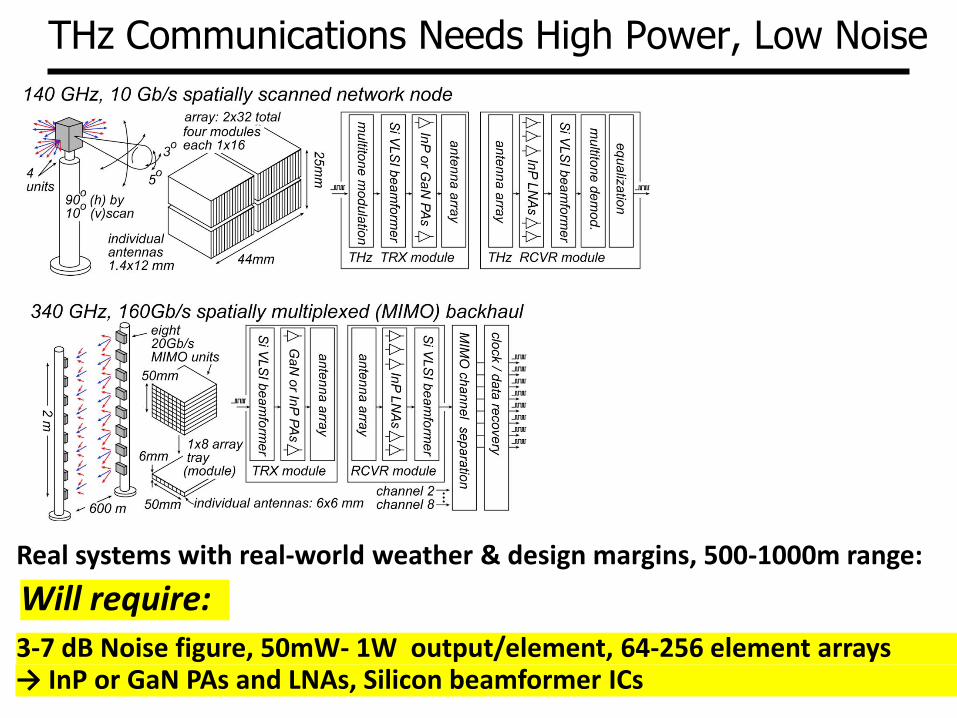
THz Communications Needs High Power, Low Noise
Real systems with real-world weather & design margins, 500-1000m range:
3-7 dB Noise figure, 50mW- 1W output/element, 64-256 element arrays
Will require:
→ InP or GaN PAs and LNAs, Silicon beamformer ICs
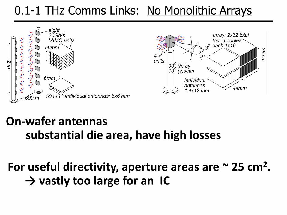
0.1-1 THz Comms Links: No Monolithic Arrays
On-wafer antennas substantial die area, have high losses
For useful directivity, aperture areas are ~ 25 cm2. → vastly too large for an IC
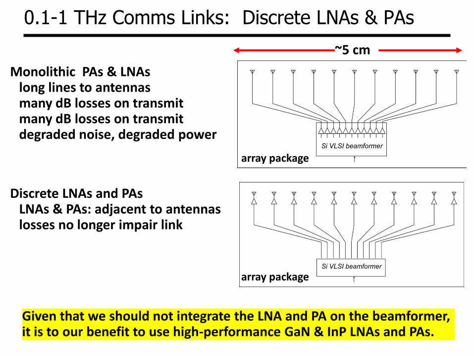
0.1-1 THz Comms Links: Discrete LNAs & PAs
Monolithic PAs & LNAs long lines to antennas many dB losses on transmit many dB losses on transmit degraded noise, degraded power
~5 cm
Discrete LNAs and PAs LNAs & PAs: adjacent to antennas losses no longer impair link
array package
array package
Given that we should not integrate the LNA and PA on the beamformer, it is to our benefit to use high-performance GaN & InP LNAs and PAs.
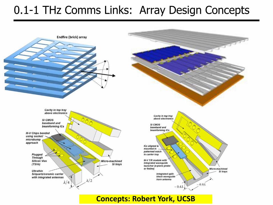
0.1-1 THz Comms Links: Array Design Concepts
Concepts: Robert York, UCSB
THz InP HBTs
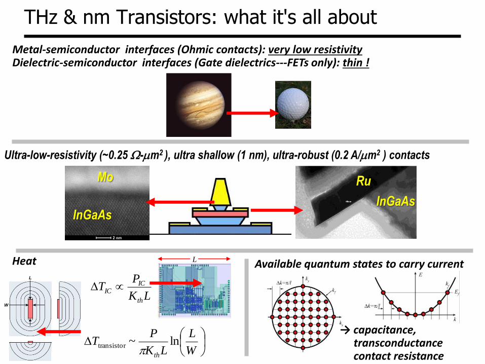
THz & nm Transistors: what it's all about
Metal-semiconductor interfaces (Ohmic contacts): very low resistivity Dielectric-semiconductor interfaces (Gate dielectrics---FETs only): thin !
Ultra-low-resistivity (~0.25 W-mm2 ), ultra shallow (1 nm), ultra-robust (0.2 A/mm2 ) contacts
Mo
InGaAs
Ru
InGaAs
Heat
W
L
LK
PT
th
ln~transistor
LK
PT
th
ICIC
Available quantum states to carry current L
→ capacitance, transconductance contact resistance

Bipolar Transistor Design eW
bcWcTbT
nbb DT 22
satcc vT 2
ELlength emitter
eex AR /contact
2
through-punchce,operatingce,max cesatc TVVAvI /)(,
contacts
contactsheet
612 AL
W
L
WR
e
bc
e
ebb
e
e
E W
L
L
PT ln1
cccb /TAC
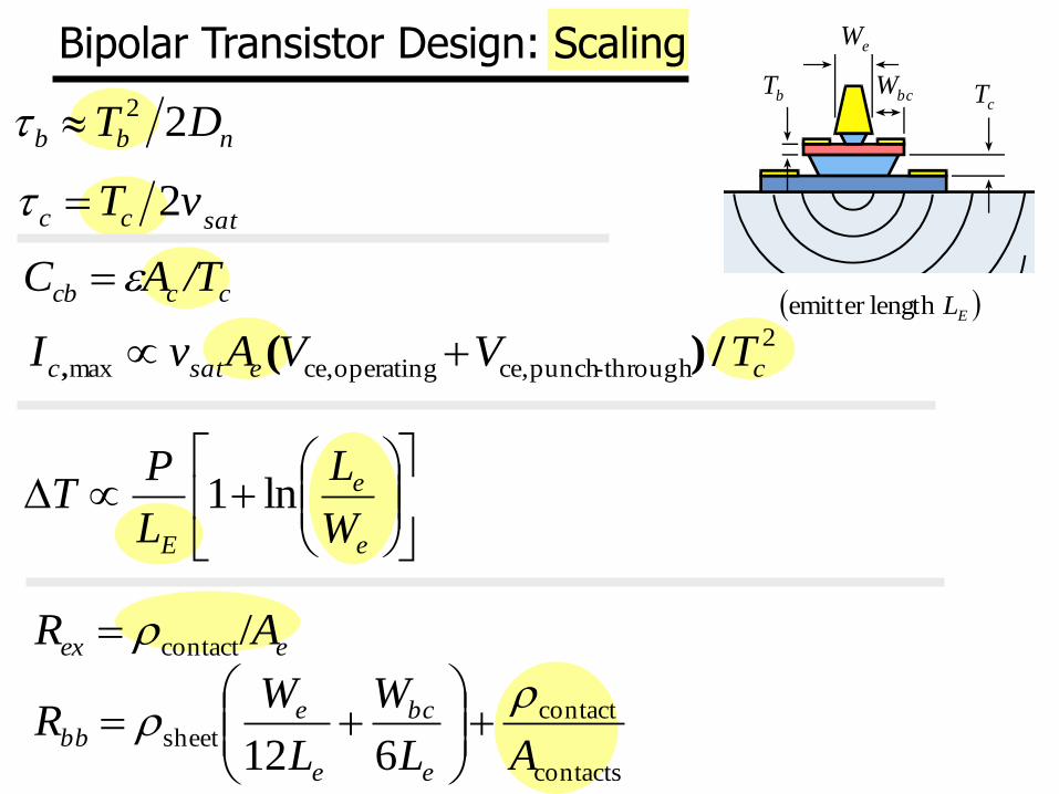
Bipolar Transistor Design: Scaling eW
bcWcTbT
nbb DT 22
satcc vT 2
ELlength emitter cccb /TAC
eex AR /contact
2
through-punchce,operatingce,max cesatc TVVAvI /)(,
contacts
contactsheet
612 AL
W
L
WR
e
bc
e
ebb
e
e
E W
L
L
PT ln1
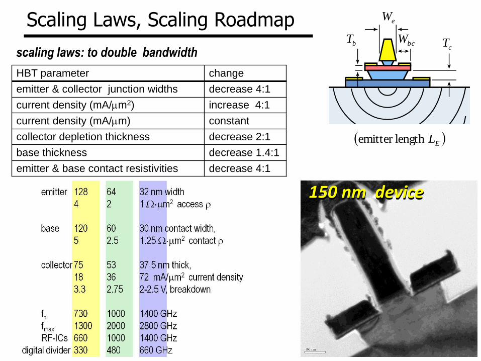
Scaling Laws, Scaling Roadmap
HBT parameter change
emitter & collector junction widths decrease 4:1
current density (mA/mm2) increase 4:1
current density (mA/mm) constant
collector depletion thickness decrease 2:1
base thickness decrease 1.4:1
emitter & base contact resistivities decrease 4:1
scaling laws: to double bandwidth
eW
bcWcTbT
ELlength emitter
150 nm device 150 nm device
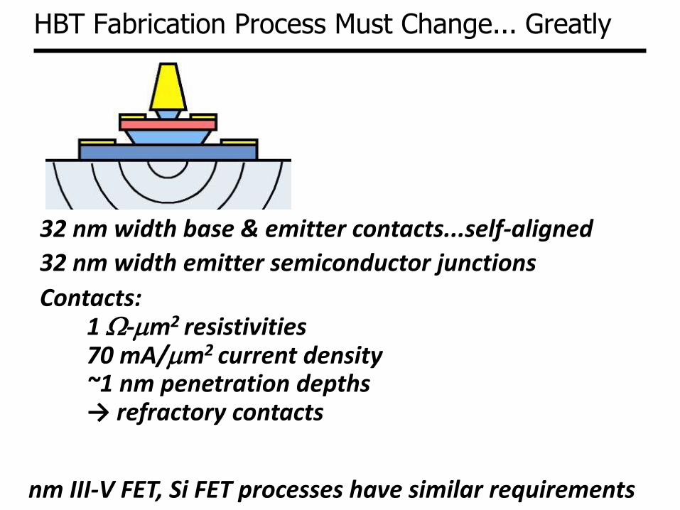
HBT Fabrication Process Must Change... Greatly
32 nm width base & emitter contacts...self-aligned
32 nm width emitter semiconductor junctions
Contacts: 1 W-mm2 resistivities 70 mA/mm2 current density ~1 nm penetration depths → refractory contacts
nm III-V FET, Si FET processes have similar requirements
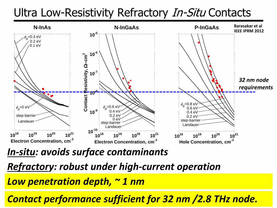
Ultra Low-Resistivity Refractory In-Situ Contacts Barasakar et al IEEE IPRM 2012
32 nm node requirements
Contact performance sufficient for 32 nm /2.8 THz node.
Low penetration depth, ~ 1 nm
In-situ: avoids surface contaminants
Refractory: robust under high-current operation
10-10
10-9
10-8
10-7
10-6
10-5
1018
1019
1020
1021
N-InGaAs
B=0.6 eV
0.4 eV0.2 eV
0 eV
Electron Concentration, cm-3
Co
nta
ct
Re
sis
tiv
ity,
W
cm
2
step-barrierLandauer
1018
1019
1020
1021
N-InAs
Electron Concentration, cm-3
0.2 eV
B=0.3 eV
step-barrier
B=0 eV
0.1 eV
Landauer
1018
1019
1020
1021
P-InGaAs
Hole Concentration, cm-3
B=0.8 eV
0.6 eV0.4 eV0.2 eV
step-barrierLandauer
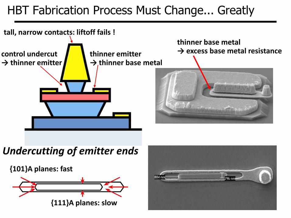
HBT Fabrication Process Must Change... Greatly
Undercutting of emitter ends
control undercut → thinner emitter
thinner emitter → thinner base metal
thinner base metal → excess base metal resistance
{101}A planes: fast
{111}A planes: slow
tall, narrow contacts: liftoff fails !
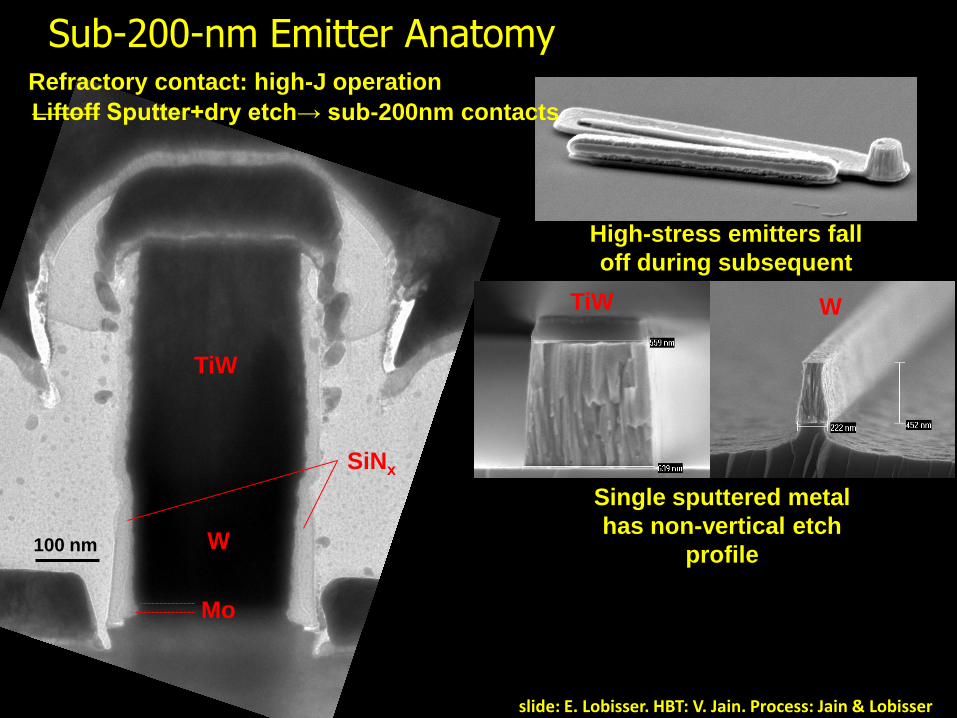
Sub-200-nm Emitter Anatomy
slide: E. Lobisser. HBT: V. Jain. Process: Jain & Lobisser
TiW
W 100 nm
Mo
High-stress emitters fall
off during subsequent
lift-offs TiW W
Single sputtered metal
has non-vertical etch
profile
SiNx
Refractory contact: high-J operation
Liftoff Sputter+dry etch→ sub-200nm contacts
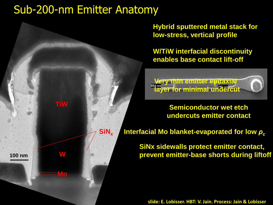
Sub-200-nm Emitter Anatomy
slide: E. Lobisser. HBT: V. Jain. Process: Jain & Lobisser
TiW
W 100 nm
Mo
Hybrid sputtered metal stack for
low-stress, vertical profile
W/TiW interfacial discontinuity
enables base contact lift-off
Interfacial Mo blanket-evaporated for low ρc SiNx
SiNx sidewalls protect emitter contact,
prevent emitter-base shorts during liftoff
Semiconductor wet etch
undercuts emitter contact
Very thin emitter epitaxial
layer for minimal undercut
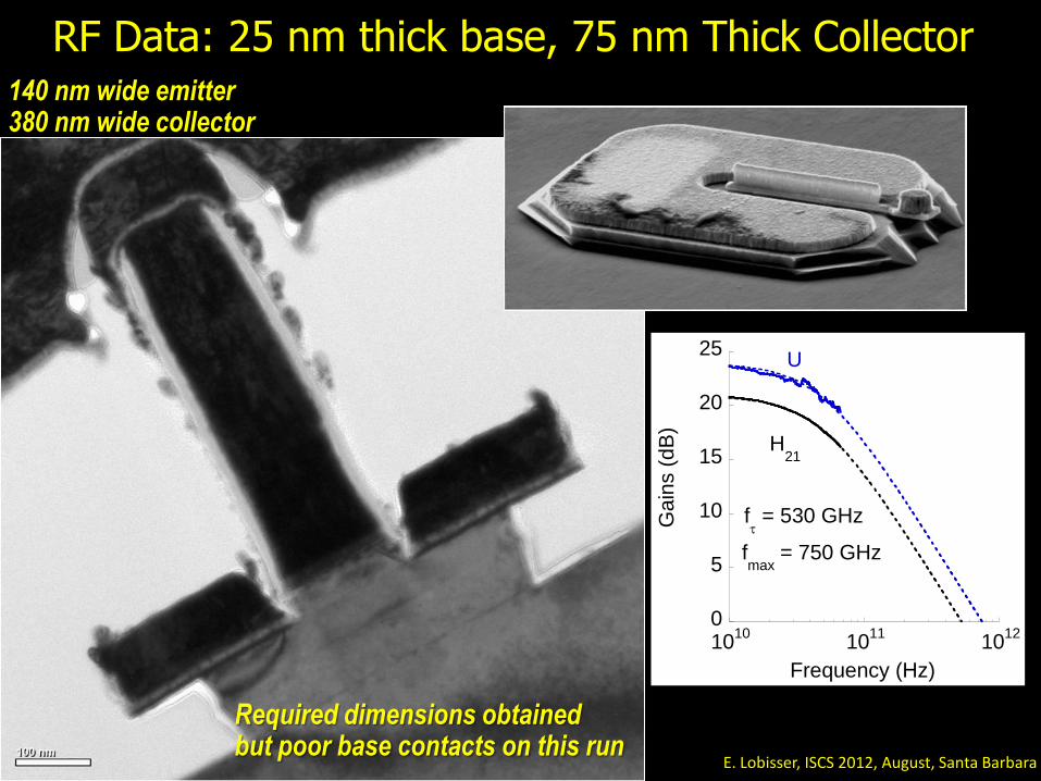
RF Data: 25 nm thick base, 75 nm Thick Collector
0
5
10
15
20
25
1010
1011
1012
Ga
ins (
dB
)Frequency (Hz)
H21
U
f = 530 GHz
fmax
= 750 GHz
Required dimensions obtained but poor base contacts on this run
E. Lobisser, ISCS 2012, August, Santa Barbara
140 nm wide emitter 380 nm wide collector
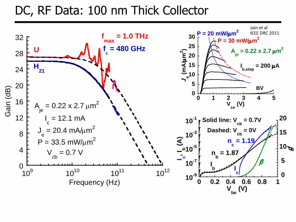
DC, RF Data: 100 nm Thick Collector
0
4
8
12
16
20
24
28
32
109
1010
1011
1012
Ga
in (
dB
)
Frequency (Hz)
U
H21
f = 480 GHz
fmax
= 1.0 THz
Aje = 0.22 x 2.7 mm
2
Ic = 12.1 mA
Je = 20.4 mA/mm
2
P = 33.5 mW/mm2
Vcb
= 0.7 V
0
5
10
15
20
25
30
0 1 2 3 4 5
Je (
mA
/mm
2)
Vce
(V)
P = 30 mW/mm2
Ib,step
= 200 mA
BV
P = 20 mW/mm2
Aje
= 0.22 x 2.7 mm2
10-9
10-7
10-5
10-3
10-1
0
5
10
15
20
0 0.2 0.4 0.6 0.8 1I c
, I b
(A
)
Vbe
(V)
Solid line: Vcb
= 0.7V
Dashed: Vcb
= 0V
nc = 1.19
nb = 1.87
Ic
Ib
Jain et al IEEE DRC 2011
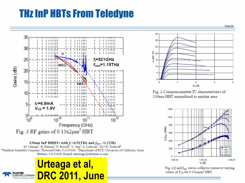
Chart 24
THz InP HBTs From Teledyne
Urteaga et al, DRC 2011, June
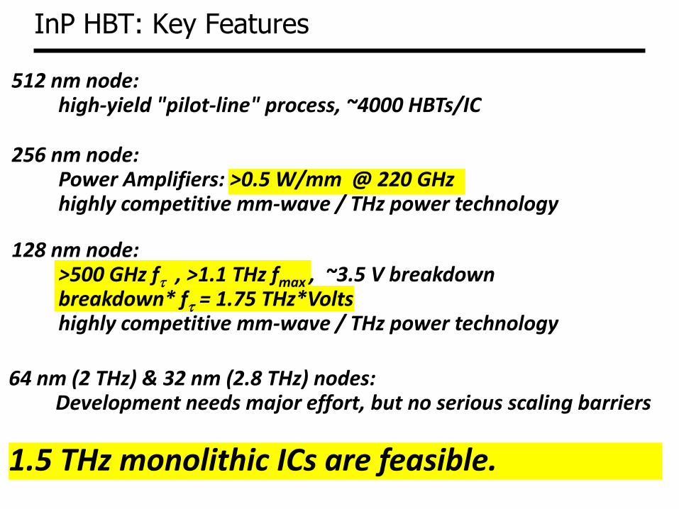
InP HBT: Key Features
512 nm node: high-yield "pilot-line" process, ~4000 HBTs/IC
256 nm node: Power Amplifiers: >0.5 W/mm @ 220 GHz highly competitive mm-wave / THz power technology
128 nm node: >500 GHz f , >1.1 THz fmax , ~3.5 V breakdown breakdown* f = 1.75 THz*Volts highly competitive mm-wave / THz power technology
64 nm (2 THz) & 32 nm (2.8 THz) nodes: Development needs major effort, but no serious scaling barriers
1.5 THz monolithic ICs are feasible.
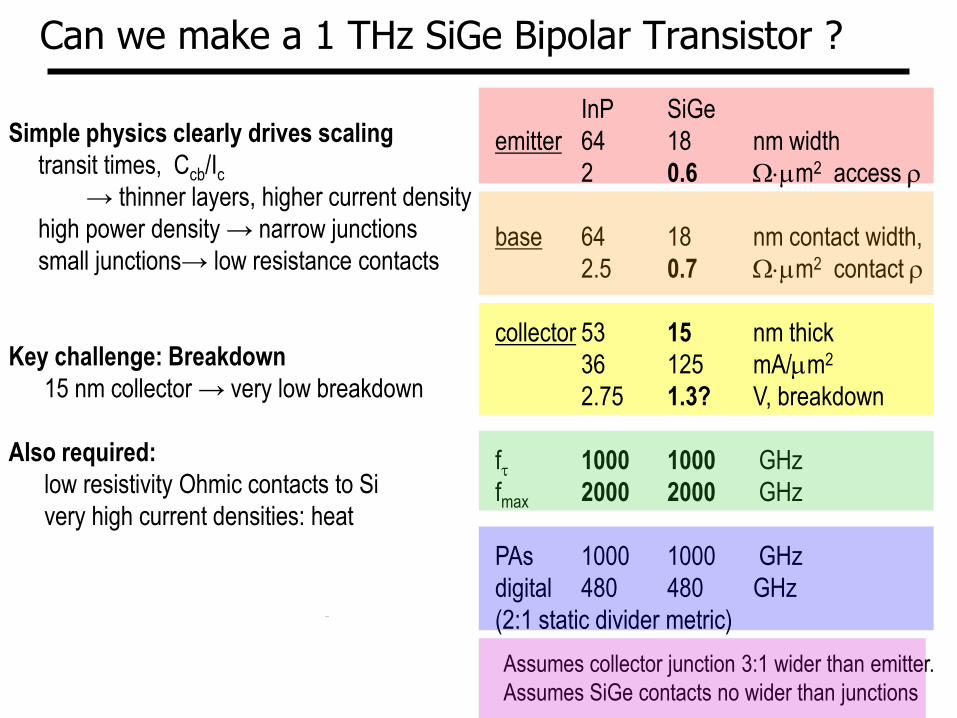
Can we make a 1 THz SiGe Bipolar Transistor ?
InP SiGe
emitter 64 18 nm width
2 0.6 Wmm2 access
base 64 18 nm contact width,
2.5 0.7 Wmm2 contact
collector 53 15 nm thick
36 125 mA/mm2
2.75 1.3? V, breakdown
f 1000 1000 GHz
fmax 2000 2000 GHz
PAs 1000 1000 GHz
digital 480 480 GHz
(2:1 static divider metric)
Assumes collector junction 3:1 wider than emitter.
Assumes SiGe contacts no wider than junctions
Simple physics clearly drives scaling
transit times, Ccb/Ic
→ thinner layers, higher current density
high power density → narrow junctions
small junctions→ low resistance contacts
Key challenge: Breakdown
15 nm collector → very low breakdown
Also required:
low resistivity Ohmic contacts to Si
very high current densities: heat

0.1-1THz IC Design
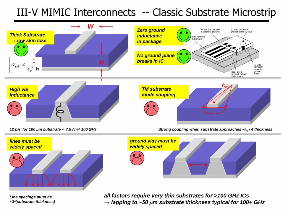
kz
III-V MIMIC Interconnects -- Classic Substrate Microstrip
Strong coupling when substrate approaches ~d / 4 thickness
H
W
Thick Substrate
→ low skin loss
Hr
skin 2/1
1
Zero ground
inductance
in package
a
Brass carrier andassembly ground
interconnectsubstrate
IC with backsideground plane & vias
near-zeroground-groundinductance
IC viaseliminateon-wafergroundloops
High via
inductance
12 pH for 100 mm substrate -- 7.5 W @ 100 GHz
TM substrate
mode coupling
Line spacings must be
~3*(substrate thickness)
lines must be
widely spaced
ground vias must be
widely spaced
all factors require very thin substrates for >100 GHz ICs
→ lapping to ~50 mm substrate thickness typical for 100+ GHz
No ground plane
breaks in IC
kz
Parasitic slot mode
-V 0V +V
0V
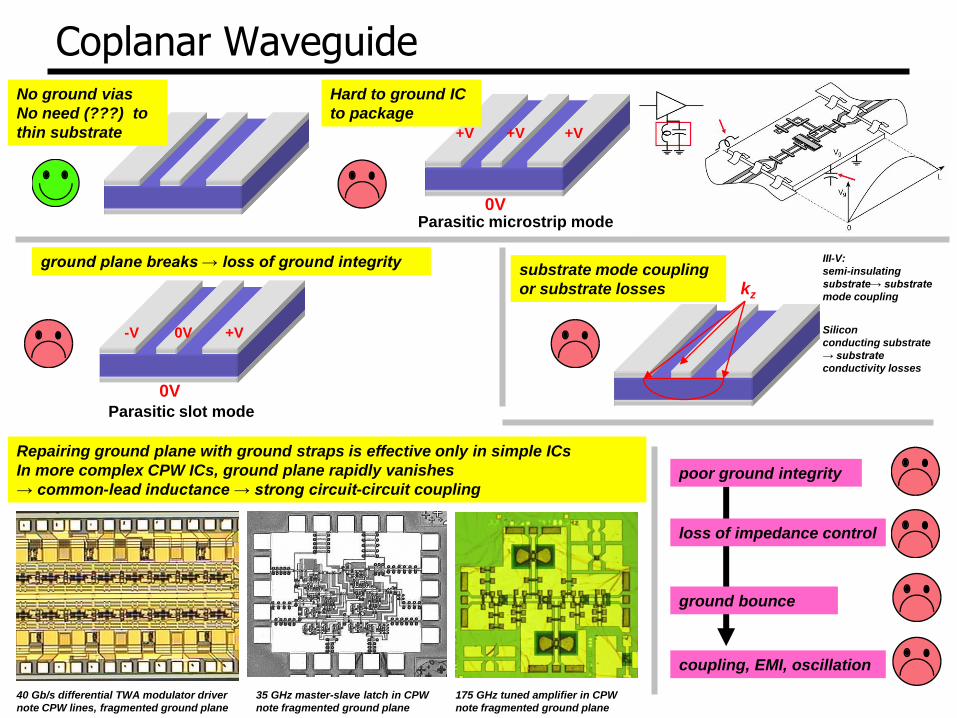
Coplanar Waveguide No ground vias
No need (???) to
thin substrate
Parasitic microstrip mode
+V +V +V
0V
Hard to ground IC
to package
substrate mode coupling
or substrate losses
ground plane breaks → loss of ground integrity
Repairing ground plane with ground straps is effective only in simple ICs
In more complex CPW ICs, ground plane rapidly vanishes
→ common-lead inductance → strong circuit-circuit coupling
40 Gb/s differential TWA modulator driver
note CPW lines, fragmented ground plane
35 GHz master-slave latch in CPW
note fragmented ground plane
175 GHz tuned amplifier in CPW
note fragmented ground plane
poor ground integrity
loss of impedance control
ground bounce
coupling, EMI, oscillation
III-V:
semi-insulating
substrate→ substrate
mode coupling
Silicon
conducting substrate
→ substrate
conductivity losses
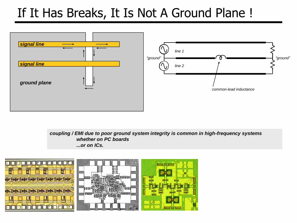
If It Has Breaks, It Is Not A Ground Plane !
signal line
signal line
ground plane
line 1
“ground”
line 2
“ground”
common-lead inductance
coupling / EMI due to poor ground system integrity is common in high-frequency systems
whether on PC boards
...or on ICs.
fewer breaks in ground plane than CPW
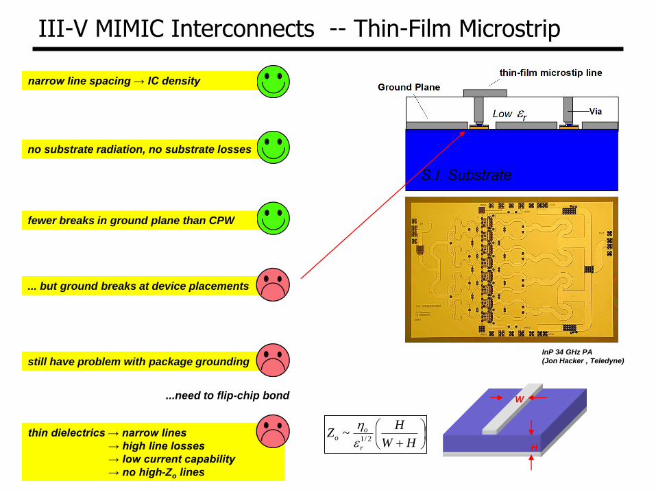
III-V MIMIC Interconnects -- Thin-Film Microstrip
narrow line spacing → IC density
... but ground breaks at device placements
still have problem with package grounding
thin dielectrics → narrow lines
→ high line losses
→ low current capability
→ no high-Zo lines
H
W
HW
HZ
r
oo 2/1
~
...need to flip-chip bond
no substrate radiation, no substrate losses
InP 34 GHz PA
(Jon Hacker , Teledyne)
No breaks in ground plane
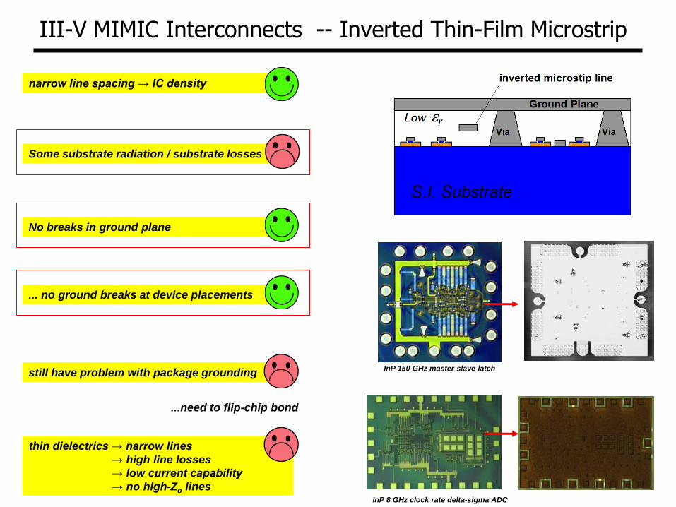
III-V MIMIC Interconnects -- Inverted Thin-Film Microstrip
narrow line spacing → IC density
... no ground breaks at device placements
still have problem with package grounding
thin dielectrics → narrow lines
→ high line losses
→ low current capability
→ no high-Zo lines
...need to flip-chip bond
Some substrate radiation / substrate losses
InP 150 GHz master-slave latch
InP 8 GHz clock rate delta-sigma ADC
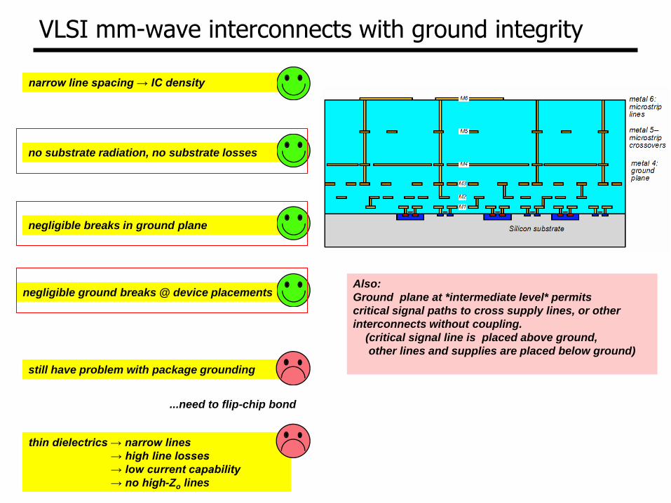
VLSI mm-wave interconnects with ground integrity
negligible breaks in ground plane
narrow line spacing → IC density
negligible ground breaks @ device placements
still have problem with package grounding
thin dielectrics → narrow lines
→ high line losses
→ low current capability
→ no high-Zo lines
...need to flip-chip bond
no substrate radiation, no substrate losses
Also:
Ground plane at *intermediate level* permits
critical signal paths to cross supply lines, or other
interconnects without coupling.
(critical signal line is placed above ground,
other lines and supplies are placed below ground)
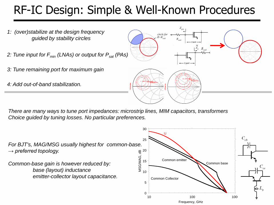
RF-IC Design: Simple & Well-Known Procedures
1: (over)stabilize at the design frequency
guided by stability circles
3: Tune remaining port for maximum gain
2: Tune input for Fmin (LNAs) or output for Psat (PAs)
4: Add out-of-band stabilization.
There are many ways to tune port impedances: microstrip lines, MIM capacitors, transformers
Choice guided by tuning losses. No particular preferences.
0
5
10
15
20
25
30
10 100 1000
MS
G/M
AG
, dB
Frequency, GHz
Common base
Common Collector
Common emitter
U
For BJT's, MAG/MSG usually highest for common-base.
→ preferred topology.
Common-base gain is however reduced by:
base (layout) inductance
emitter-collector layout capacitance.
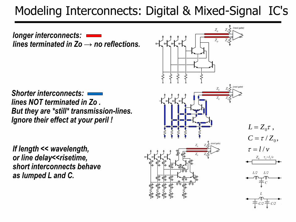
Modeling Interconnects: Digital & Mixed-Signal IC's
longer interconnects: lines terminated in Zo → no reflections.
Shorter interconnects: lines NOT terminated in Zo . But they are *still* transmission-lines. Ignore their effect at your peril !
vl
ZC
ZL
/
,/
,
0
0
If length << wavelength, or line delay<<risetime, short interconnects behave as lumped L and C.
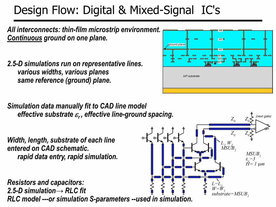
Design Flow: Digital & Mixed-Signal IC's
All interconnects: thin-film microstrip environment. Continuous ground on one plane.
2.5-D simulations run on representative lines. various widths, various planes same reference (ground) plane.
Simulation data manually fit to CAD line model effective substrate r , effective line-ground spacing.
Width, length, substrate of each line entered on CAD schematic. rapid data entry, rapid simulation.
Resistors and capacitors: 2.5-D simulation→ RLC fit RLC model ---or simulation S-parameters --used in simulation.
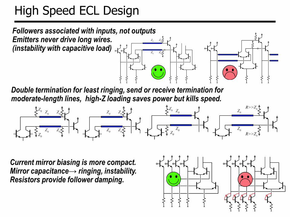
High Speed ECL Design
Followers associated with inputs, not outputs Emitters never drive long wires. (instability with capacitive load)
Double termination for least ringing, send or receive termination for moderate-length lines, high-Z loading saves power but kills speed.
Current mirror biasing is more compact. Mirror capacitance→ ringing, instability. Resistors provide follower damping.

High Speed ECL Design
Layout: short signal paths at gate centers, bias sources surround core. Inverted thin film microstrip wiring.
Example: 8:1 205 GHz static divider in 256 nm InP HBT.
Key: transistors in on-state operate at Kirk limited-current. → minimizes Ccb/Ic delay.
205 GHz divider, Griffith et al, IEEE CSIC, Oct. 2010
Key: transistors designed for minimum ECL gate delay*, not peak (f , fmax). *hand expression, charge-control analysis
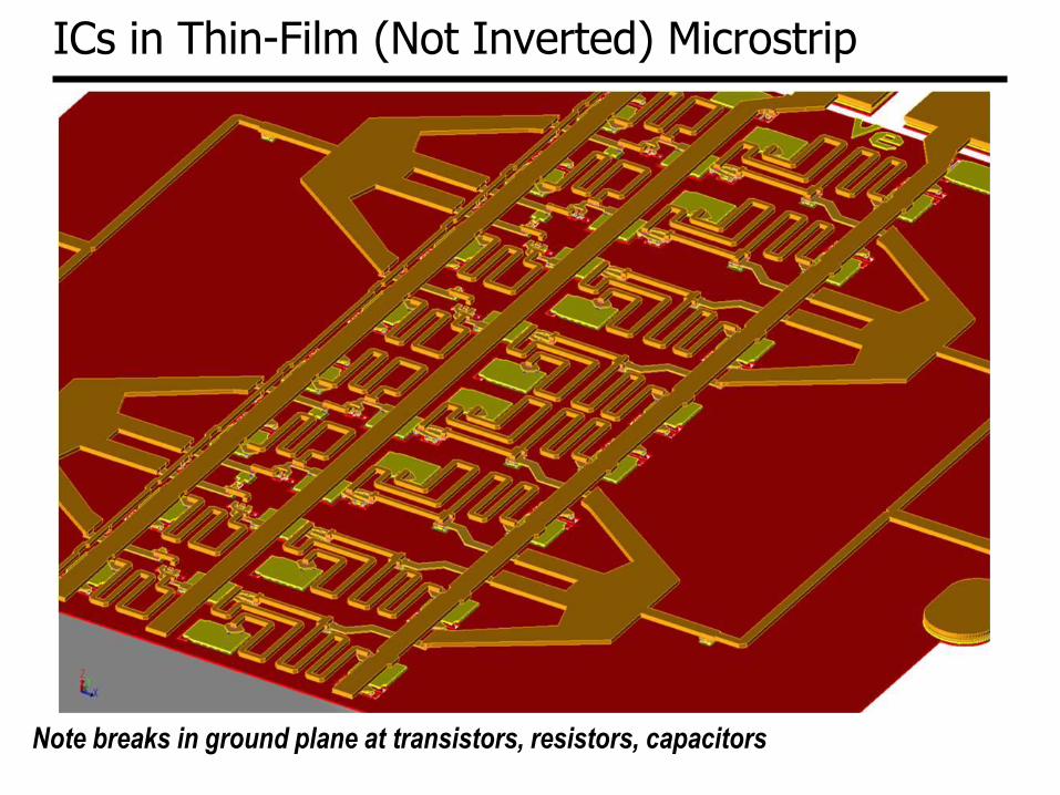
ICs in Thin-Film (Not Inverted) Microstrip
Note breaks in ground plane at transistors, resistors, capacitors
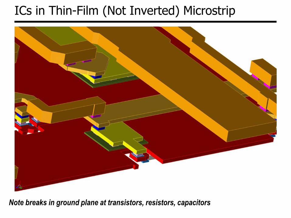
ICs in Thin-Film (Not Inverted) Microstrip
Note breaks in ground plane at transistors, resistors, capacitors
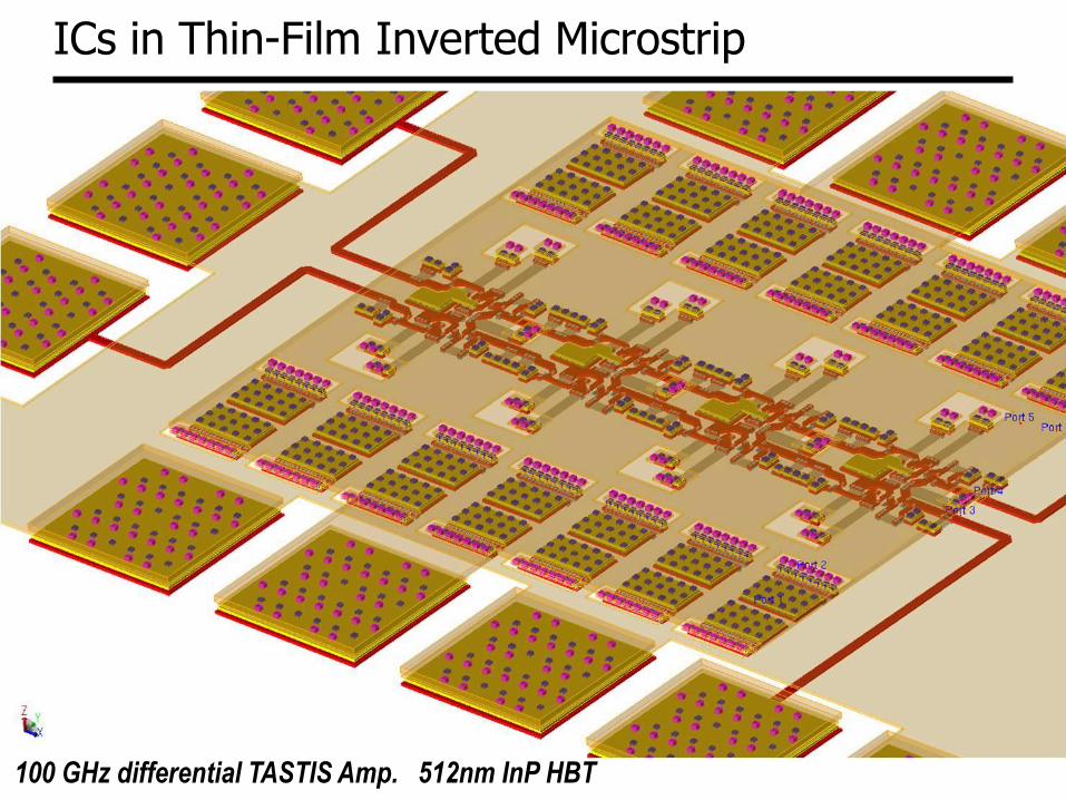
ICs in Thin-Film Inverted Microstrip
100 GHz differential TASTIS Amp. 512nm InP HBT
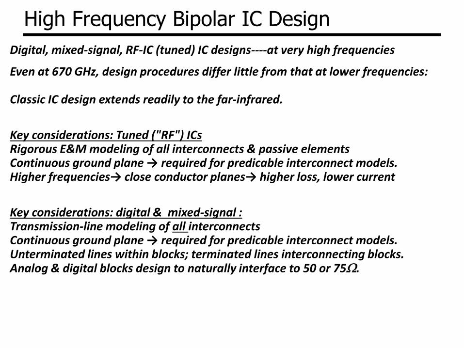
High Frequency Bipolar IC Design
Digital, mixed-signal, RF-IC (tuned) IC designs----at very high frequencies
Even at 670 GHz, design procedures differ little from that at lower frequencies: Classic IC design extends readily to the far-infrared.
Key considerations: Tuned ("RF") ICs Rigorous E&M modeling of all interconnects & passive elements Continuous ground plane → required for predicable interconnect models. Higher frequencies→ close conductor planes→ higher loss, lower current
Key considerations: digital & mixed-signal : Transmission-line modeling of all interconnects Continuous ground plane → required for predicable interconnect models. Unterminated lines within blocks; terminated lines interconnecting blocks. Analog & digital blocks design to naturally interface to 50 or 75W.

Design Examples, IC Results
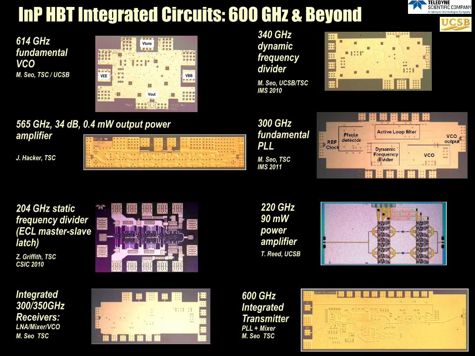
InP HBT Integrated Circuits: 600 GHz & Beyond
614 GHz fundamental VCO
340 GHz dynamic frequency divider
Vout
VEE VBB
Vtune
Vout
VEE VBB
Vtune
565 GHz, 34 dB, 0.4 mW output power amplifier
J. Hacker, TSC
M. Seo, TSC / UCSB
M. Seo, UCSB/TSC IMS 2010
204 GHz static frequency divider (ECL master-slave latch)
Z. Griffith, TSC CSIC 2010
300 GHz fundamental PLL M. Seo, TSC IMS 2011
220 GHz 90 mW power amplifier T. Reed, UCSB
600 GHz Integrated Transmitter PLL + Mixer M. Seo TSC
Integrated 300/350GHz Receivers: LNA/Mixer/VCO
M. Seo TSC
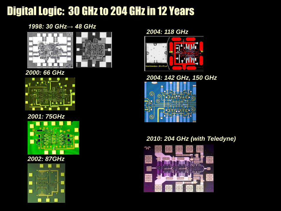
Digital Logic: 30 GHz to 204 GHz in 12 Years
2000: 66 GHz
1998: 30 GHz→ 48 GHz
2001: 75GHz
2002: 87GHz
2004: 118 GHz
2004: 142 GHz, 150 GHz
2010: 204 GHz (with Teledyne)
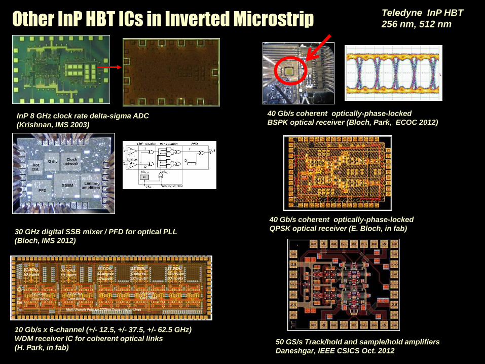
Other InP HBT ICs in Inverted Microstrip
InP 8 GHz clock rate delta-sigma ADC
(Krishnan, IMS 2003)
30 GHz digital SSB mixer / PFD for optical PLL
(Bloch, IMS 2012)
10 Gb/s x 6-channel (+/- 12.5, +/- 37.5, +/- 62.5 GHz)
WDM receiver IC for coherent optical links
(H. Park, in fab)
40 Gb/s coherent optically-phase-locked
BSPK optical receiver (Bloch, Park, ECOC 2012)
40 Gb/s coherent optically-phase-locked
QPSK optical receiver (E. Bloch, in fab)
50 GS/s Track/hold and sample/hold amplifiers
Daneshgar, IEEE CSICS Oct. 2012
Teledyne InP HBT
256 nm, 512 nm
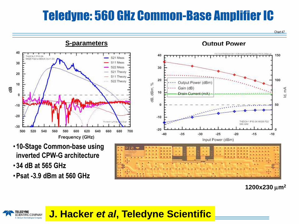
Chart 47
Teledyne: 560 GHz Common-Base Amplifier IC
S-parameters Output Power
•10-Stage Common-base using
inverted CPW-G architecture
•34 dB at 565 GHz
•Psat -3.9 dBm at 560 GHz
1200x230 mm2
J. Hacker et al, Teledyne Scientific

Chart 48
130nm 600 GHz Fundamental Oscillators
Output spectrum measurements performed on-wafer using UVA Wafer probes and Virginia Diodes VNA Extender Heads
Single-ended power measurements performed with on-wafer probe coupled to Erickson calorimeter power meter. Pout corrected based on measured probe loss at osc. frequency.
Output spectrum of 614GHz oscillator
fabricated with 130nm HBTs
Oscillator Output Power
610 GHz
598GHz
570GHz
560GHz
540GHz
Measured Freq.
-17.8
-13.8
-14.1
-19.2
Measure Pout
(dBm)
-10.1
610 GHz
598GHz
570GHz
560GHz
540GHz
Measured Freq.
-17.8
-13.8
-14.1
-19.2
Measure Pout
(dBm)
-10.1
Oscillator Schematic
M. Seo et al, Teledyne Scientific
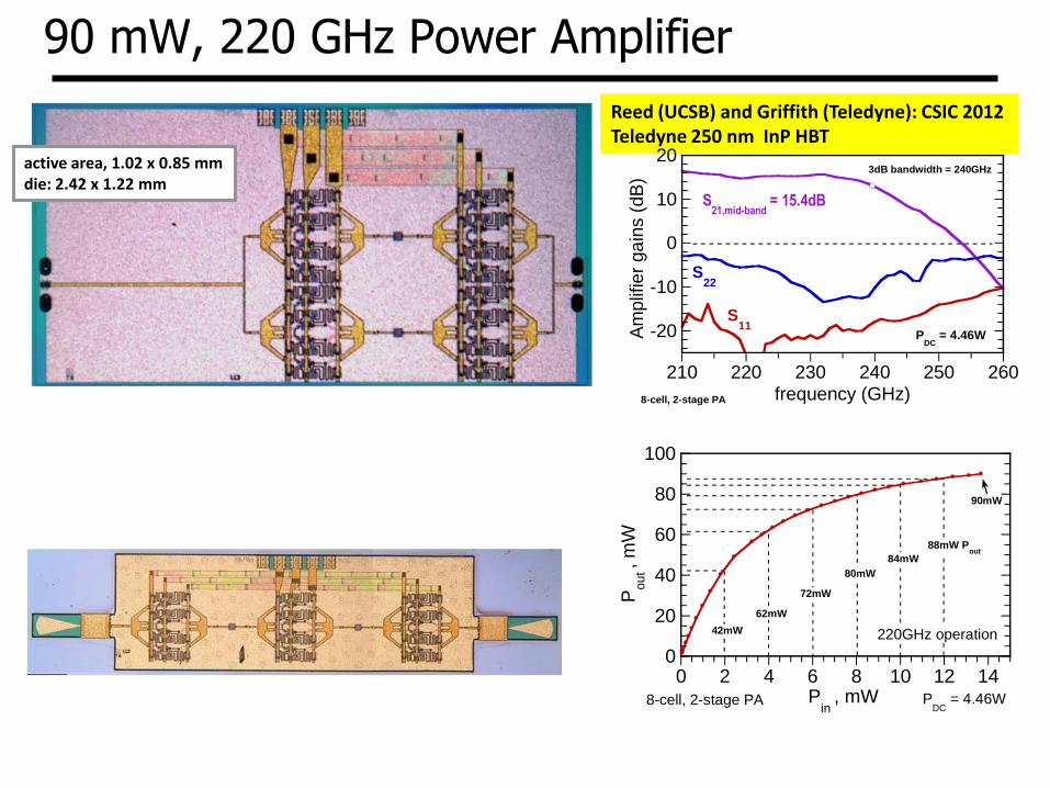
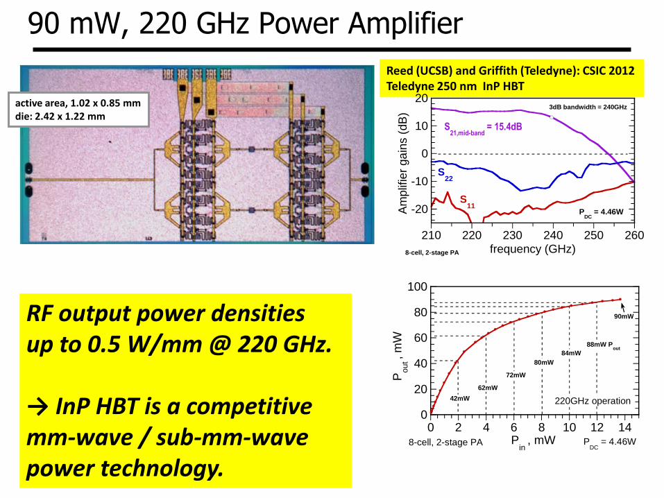
90 mW, 220 GHz Power Amplifier
Reed (UCSB) and Griffith (Teledyne): CSIC 2012 Teledyne 250 nm InP HBT
-20
-10
0
10
20
210 220 230 240 250 260
Am
plif
ier
ga
ins (
dB
)
frequency (GHz)
3dB bandwidth = 240GHz
S21,mid-band
= 15.4dB
S11
S22
8-cell, 2-stage PA
PDC
= 4.46W
0
20
40
60
80
100
0 2 4 6 8 10 12 14
Pou
t , m
W
Pin
, mW8-cell, 2-stage PA PDC
= 4.46W
88mW Pout
84mW
80mW
72mW
62mW
42mW
90mW
220GHz operation
active area, 1.02 x 0.85 mm die: 2.42 x 1.22 mm
90 mW, 220 GHz Power Amplifier
Reed (UCSB) and Griffith (Teledyne): CSIC 2012 Teledyne 250 nm InP HBT
-20
-10
0
10
20
210 220 230 240 250 260
Am
plif
ier
ga
ins (
dB
)
frequency (GHz)
3dB bandwidth = 240GHz
S21,mid-band
= 15.4dB
S11
S22
8-cell, 2-stage PA
PDC
= 4.46W
0
20
40
60
80
100
0 2 4 6 8 10 12 14
Pou
t , m
W
Pin
, mW8-cell, 2-stage PA PDC
= 4.46W
88mW Pout
84mW
80mW
72mW
62mW
42mW
90mW
220GHz operation
RF output power densities up to 0.5 W/mm @ 220 GHz. → InP HBT is a competitive mm-wave / sub-mm-wave power technology.
active area, 1.02 x 0.85 mm die: 2.42 x 1.22 mm
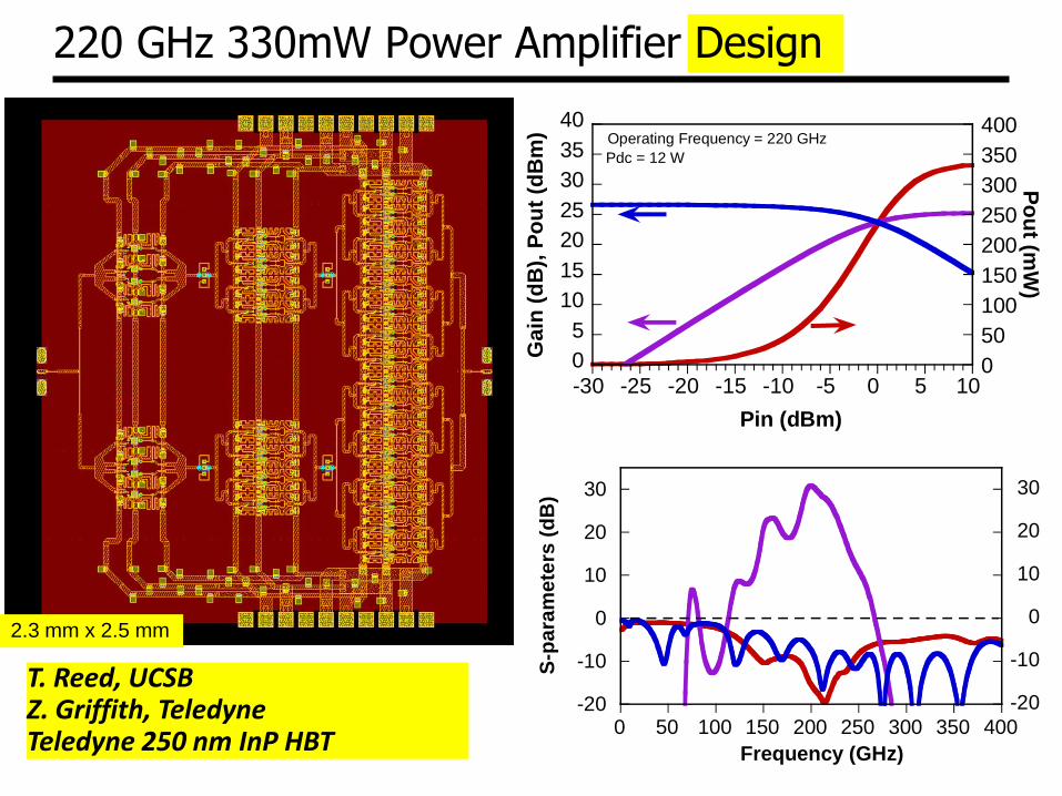
220 GHz 330mW Power Amplifier Design
0
5
10
15
20
25
30
35
40
0
50
100
150
200
250
300
350
400
-30 -25 -20 -15 -10 -5 0 5 10
Ga
in (
dB
), P
ou
t (d
Bm
)
Po
ut (m
W)
Pin (dBm)
Operating Frequency = 220 GHz
Pdc = 12 W
-20
-10
0
10
20
30
0 50 100 150 200 250 300 350 400
-20
-10
0
10
20
30
S-p
ara
me
ters
(d
B)
Frequency (GHz)
2.3 mm x 2.5 mm
T. Reed, UCSB Z. Griffith, Teledyne Teledyne 250 nm InP HBT

220 GHz Vector Modulator / Phase Shifter Design
0o
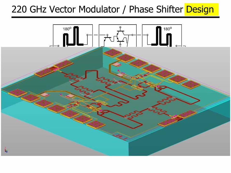
220 GHz Vector Modulator / Phase Shifter Design
0o
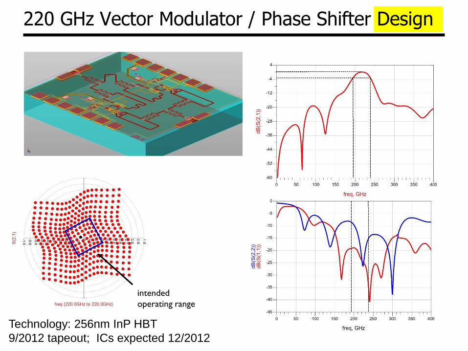
220 GHz Vector Modulator / Phase Shifter Design
intended
operating range
Technology: 256nm InP HBT
9/2012 tapeout; ICs expected 12/2012

Closing
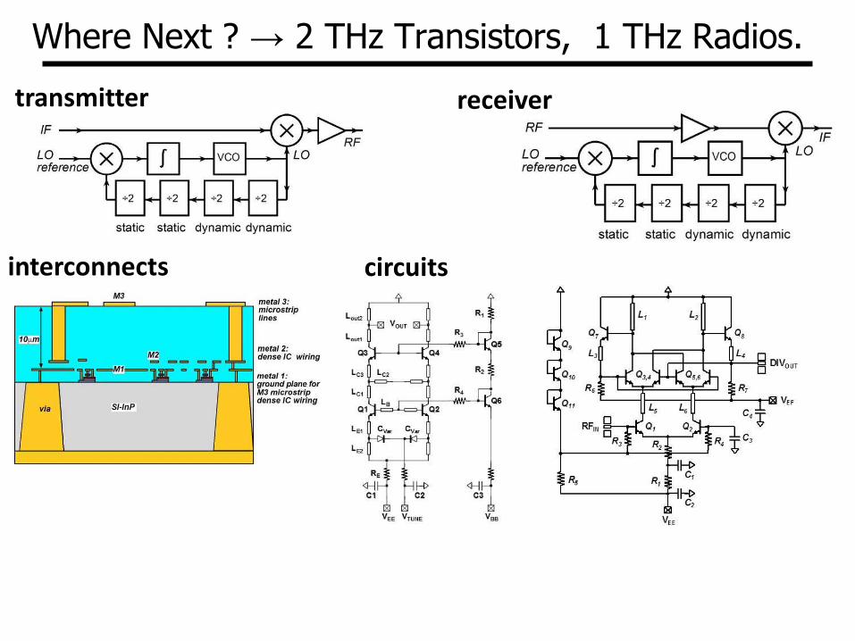
Where Next ? → 2 THz Transistors, 1 THz Radios.
transmitter receiver
interconnects circuits

THz and Far-Infrared Electronics
IR today→ lasers & bolometers → generate & detect
Far-infrared ICs: classic device physics, classic circuit design
Power, power-added efficiency, noise figure are all very important
Even 1-3 THz ICs will be feasible
The transistors will scale to at least 2 THz bandwidths
fundamental-mode operation, not harmonic generation
(backup slides follow)

At High Frequencies The Atmosphere Is Opaque Mark Rosker
IEEE IMS 2007
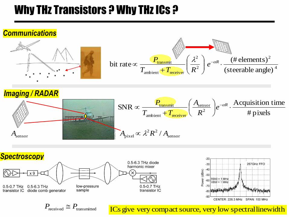
Why THz Transistors ? Why THz ICs ?
Communications
sensor
22
pixel / ARA sensorA
Imaging / RADAR
pixels #
n timeAcquisitio SNR
2
sensor
receiverambient
transmit
Re
R
A
TT
P
Spectroscopy
4
2
2
2
receiverambient
transmit
angle) steerable(
elements) (# ratebit
Re
RTT
P
dtransmittereceived PP linewidth spectral low very source,compact very give ICs