The World of Compound Semiconductorsjytsao/WCS.pdfCompound III-V Semiconductors A new family of...
191
7/14/2004 World of Compound Semiconductors Page 1 of 191 T T h h e e W W o o r r l l d d o o f f C C o o m m p p o o u u n n d d S S e e m m i i c c o o n n d d u u c c t t o o r r s s A A G G u u i i d d e e b b o o o o k k t t o o t t h h e e C C o o r r e e S S c c i i e e n n c c e e a a n n d d T T e e c c h h n n o o l l o o g g y y Jeff Y Tsao -- Sandia National Laboratories … -- … -- … -- … -- … -- … -- … --
Transcript of The World of Compound Semiconductorsjytsao/WCS.pdfCompound III-V Semiconductors A new family of...
7/14/2004 World of Compound Semiconductors Page 1 of 191
TThhee WWoorrlldd ooff CCoommppoouunndd SSeemmiiccoonndduuccttoorrss
AA GGuuiiddeebbooookk ttoo tthhee CCoorree SScciieennccee aanndd TTeecchhnnoollooggyy
JJeeffff YY TTssaaoo ---- SSaannddiiaa NNaattiioonnaall LLaabboorraattoorriieess …… ---- …… ---- …… ---- …… ---- …… ---- …… ---- …… ----
7/14/2004 World of Compound Semiconductors Page 2 of 191
0.1 Scope
Compound III-V Semiconductors A new family of semiconductors is changing the
way we live. These semiconductors are in our cell phones, in our optical-fiber communications systems, in our CD and DVD players, and soon in our home and office lights. They are called compound semiconductors, because they are compounds of two or more elements.
This book is a guide to the science, technology, and applications of the most important of these semiconductors, composed of one element from column III, and one from column V, of the Periodic Table -- the so-called compound III-V semiconductors, such as GaAs, InP and GaN.
IV’s, III-V’s, II-VI’s, I-VII’s These compound III-V semiconductors are a
subset of the universe of simple ANB8-N binary octet compounds, whose outer orbitals are filled with exactly 8 electrons: the elemental column IV semiconductors Ge, Si and C, the compound II-VI semiconductors such as ZnSe and CdS, and the compound I-VII semiconductor/insulators such as NaCl and LiF.
In many ways, all the semiconductors in the universe of simple octet compounds are similar. As semiconductors, their electrical conductivities are “intermediate” between those of metals and insulators. And, as semiconductors, their electrical conductivities can be modified by electric fields, enabling switching, amplification, and other electronic functions. Hence, if only the simplest semiconducting properties are required, for modest-performance electronics, it is the most abundant, most economical-to-process semiconductor that dominates: the elemental column IV semiconductor Si.
However, in many other ways, the compound III-V semiconductors are unique within the universe of simple octet compounds, enabling them to dominate higher performance electronics and optoelectronics.
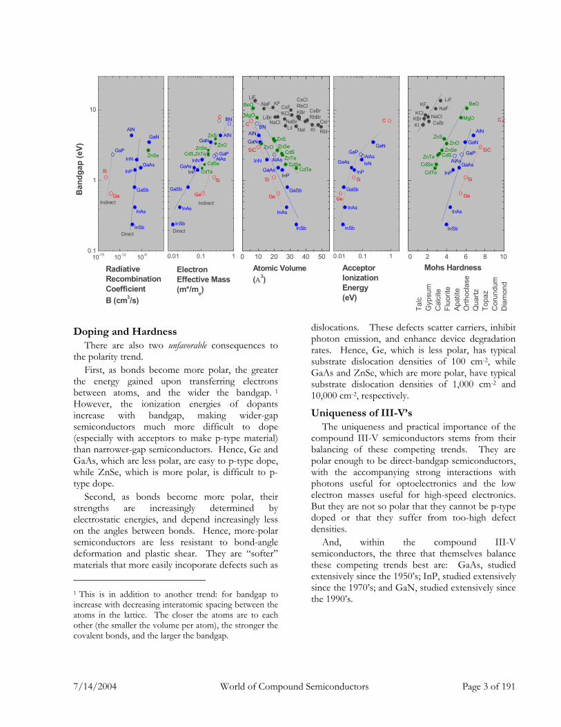
One way to think of this uniqueness is in terms of the trend for bonds between atoms to become more polar in moving “outwards” in the Periodic Table from the column IV semiconductors to the III-V’s, II-VI’s and I-VII’s. These trends are illustrated in the Facing Figure, which shows a visual map of the key properties of the simple binary octet semiconductors.
Direct Bandgaps There are two favorable consequences to the
polarity trend. Both stem from the tendency, as bonds become more polar, for bandgaps to become “direct” (filled symbols) rather than “indirect” (open symbols). In other words, electrons at the bottom of the normally-unfilled conduction band have the same k=0 momentum as electrons at the top of the normally-filled valence band.
First, valence electrons can absorb photons and become conduction electrons, and conduction electrons can emit photons and become valence electrons, both without phonons that otherwise might be needed to conserve momentum. Moving outwards from Column IV of the Periodic Table, Ge is “indirect,” has a lower radiative recombination coefficient, and is less useful for optoelectronics. GaAs and ZnSe are “direct,” have higher radiative recombination coefficients, and are more useful for optoelectronics. Hence, today’s most efficient and highest-power commercial semiconductor lasers are based on GaAs.
Second, electron masses in the “direct gap” k=0 electron states are usually lower than in the “indirect gap” k≠0 electron states. Ge, which is less ionic, is indirect, and has a higher electron effective mass less useful for high-speed electronics; while GaAs and ZnSe are more ionic, are direct, and have lower electron masses more useful for high-speed electronics. Hence, today’s most efficient and highest-speed commercial semiconductor amplifiers are based on GaAs.
Ia IIa IIb IIIa IVa Va VIa VIIa VIIIa
H He
Li Be B C N O F Ne
Na Mg Al Si P S Cl Ar
K Ca Zn Ga Ge As Se Br Kr
Rb Sr Cd In Sn Sb Te I Xe
Cs Ba Hg Tl Pb Bi Po At Rn
7/14/2004 World of Compound Semiconductors Page 3 of 191
Doping and Hardness There are also two unfavorable consequences to
the polarity trend. First, as bonds become more polar, the greater
the energy gained upon transferring electrons between atoms, and the wider the bandgap. 1 However, the ionization energies of dopants increase with bandgap, making wider-gap semiconductors much more difficult to dope (especially with acceptors to make p-type material) than narrower-gap semiconductors. Hence, Ge and GaAs, which are less polar, are easy to p-type dope, while ZnSe, which is more polar, is difficult to p-type dope.
Second, as bonds become more polar, their strengths are increasingly determined by electrostatic energies, and depend increasingly less on the angles between bonds. Hence, more-polar semiconductors are less resistant to bond-angle deformation and plastic shear. They are “softer” materials that more easily incoporate defects such as 1 This is in addition to another trend: for bandgap to increase with decreasing interatomic spacing between the atoms in the lattice. The closer the atoms are to each other (the smaller the volume per atom), the stronger the covalent bonds, and the larger the bandgap.
dislocations. These defects scatter carriers, inhibit photon emission, and enhance device degradation rates. Hence, Ge, which is less polar, has typical substrate dislocation densities of 100 cm-2, while GaAs and ZnSe, which are more polar, have typical substrate dislocation densities of 1,000 cm-2 and 10,000 cm-2, respectively.
Uniqueness of III-V’s The uniqueness and practical importance of the
compound III-V semiconductors stems from their balancing of these competing trends. They are polar enough to be direct-bandgap semiconductors, with the accompanying strong interactions with photons useful for optoelectronics and the low electron masses useful for high-speed electronics. But they are not so polar that they cannot be p-type doped or that they suffer from too-high defect densities.
And, within the compound III-V semiconductors, the three that themselves balance these competing trends best are: GaAs, studied extensively since the 1950’s; InP, studied extensively since the 1970’s; and GaN, studied extensively since the 1990’s.
0 10 20 30 40 50
NaCl NaBr LiI
CsClRbClKBr CsBr
RbBrCsI
RbI
InN
GaSb
BN
Atomic Volume(Α3)
Ge
Si
SiC
C
InSb
InAs
InPGaAs
GaNAlN
NaI
CsFKCl
KI
LiFBeO
ZnO
MgO
AlAs
ZnSZnSe
CdSe
CdS
CdTe
ZnTe
NaF
LiBr
KF
10-15 10-12 10-90.1
1
10
ZnSe
Direct
Indirect
GaSb
InN
Ban
dgap
(eV)
RadiativeRecombinationCoefficientB (cm3/s)
InSb
InAs
InPGaAs
GaP
GaNAlN
Ge
Si
0.01 0.1 1
GaPAlAs
ZnSe ZnO
ZnS
CdS,ZnTe
CdTeCdSe
BN
ElectronEffective Mass(m*/mo)
Indirect
DirectInSb
InAs
GaSb
InPGaAs
InN
GaNAlN
Ge
Si
C
0.01 0.1 1
GaN
GaSb
AcceptorIonizationEnergy(eV)
InSb
InAs
InP
GaAs InNAlAs
GaP
Ge
Si
C
0 2 4 6 8 10
CsBr
KClKBrKI
LiFBeO
ZnO
MgO
GaPAlAs
InP
GaN
AlN
InAs
GaAs
InSb
C
SiC
Si
Mohs Hardness
Talc
Gyp
sum
Cal
cite
Fluo
rite
Apat
iteO
rthoc
lase
Qua
rtzTo
paz
Cor
undu
mD
iam
ond
Ge
ZnS
ZnSe
CdSe
CdS
CdTe
ZnTe
NaFNaCl
KF
7/14/2004 World of Compound Semiconductors Page 4 of 191
0.2 Audience and Format
Audience Because of the unique properties of the
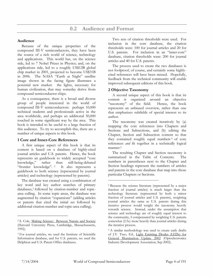
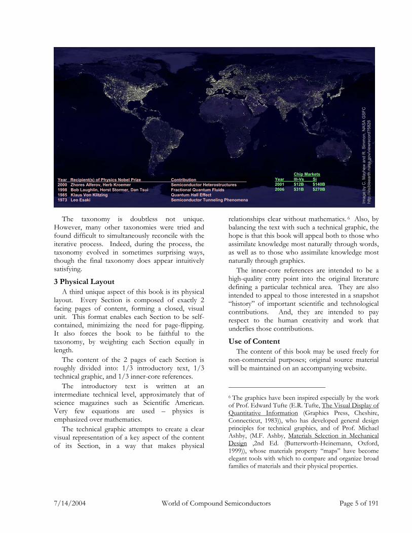
compound III-V semiconductors, they have been the source of a rich world of science, technology and applications. This world has, on the science side, led to 7 Nobel Prizes in Physics; and, on the applications side, led to a roughly US$12B global chip market in 2001, projected to become US$31B in 2006. The NASA “Earth at Night” satellite image shown in the facing figure illustrates a potential new market: the lights, necessary for human civilization, that may someday derive from compound semiconductor chips.
As a consequence, there is a broad and diverse group of people interested in the world of compound III-V semiconductors: perhaps 10,000 technical students and professionals active in the area worldwide, and perhaps an additional 50,000 touched in some significant way by the area. This book is intended to be useful to a large fraction of this audience. To try to accomplish this, there are a number of unique aspects to this book.
1 Core and Inner-Core References A first unique aspect of this book is that its
content is based on a database of highly-cited journal articles and U.S. patents. Hence, the book represents an guidebook to widely accepted “core knowledge,” rather than still-being-debated “frontier knowledge”. 2 It also represents a guidebook to both science (represented by journal articles) and technology (represented by patents).
The database was created using a combination of key word and key author searches of primary databases,3 followed by citation-number and topic-area culling. In some topic areas, the database was augmented by citation “expansions” (adding articles or patents that cited the initial set followed by additional citation-number and topic-area culling).
2 S. Cole, Making Science: Between Nature and Society (Harvard University Press, Cambridge, Massachussetts, 1992). 3 For journal articles, we used the Institute of Scientific Information database, and for U.S. patents, we used the Delphion and U.S. Patent Office databases.
Two sets of citation thresholds were used. For inclusion in the core database, the citation thresholds were: 100 for journal articles and 20 for U.S. patents. For inclusion in an “inner-core” database, citation thresholds were: 200 for journal articles and 40 for U.S. patents.
The process used to create the two databases is not foolproof, of course, and certainly some highly-cited references will have been missed. Hopefully, feedback from the technical community will enable improved subsequent editions of this book.
2 Objective Taxonomy A second unique aspect of this book is that its
content is organized around an objective “taxonomy” of the field. Hence, the book represents an unbiased overview, rather than one that emphasizes subfields of special interest to its author.
The taxonomy was created iteratively by (a) mapping the core references into Chapters and Sections and Subsections, and (b) editing the Chapter, Section and Subsection content so that they contained roughly equal numbers 4 of core references and fit together in a technically logical manner.5
The resulting Chapter and Section taxonomy is summarized in the Table of Contents. The numbers in parentheses next to the Chapter and Section headings represent the numbers of articles and patents in the core database that map into those particular Chapters or Sections. 4 Because the science literature (represented by a major fraction of journal articles) is much larger than the technology literature (represented by both a minor fraction of journal articles and U.S. patents), weighting journal articles the same as U.S. patents during this iterative process would weight the taxonomy heavily towards science. Instead, under the assumption that science and technology are of roughly equal interest to the community, I compensated by weighting U.S. patents somewhat (2.5x) more heavily than journal articles during the iterative process. 5 A similar methodology was used to create early drafts of J.Y. Tsao, Ed., Light Emitting Diodes (LEDs) for General Illumination Update 2002 (Optoelectronics Industry Development Association, Sep 2002).
7/14/2004 World of Compound Semiconductors Page 5 of 191
The taxonomy is doubtless not unique. However, many other taxonomies were tried and found difficult to simultaneously reconcile with the iterative process. Indeed, during the process, the taxonomy evolved in sometimes surprising ways, though the final taxonomy does appear intuitively satisfying.
3 Physical Layout A third unique aspect of this book is its physical
layout. Every Section is composed of exactly 2 facing pages of content, forming a closed, visual unit. This format enables each Section to be self-contained, minimizing the need for page-flipping. It also forces the book to be faithful to the taxonomy, by weighting each Section equally in length.
The content of the 2 pages of each Section is roughly divided into: 1/3 introductory text, 1/3 technical graphic, and 1/3 inner-core references.
The introductory text is written at an intermediate technical level, approximately that of science magazines such as Scientific American. Very few equations are used – physics is emphasized over mathematics.
The technical graphic attempts to create a clear visual representation of a key aspect of the content of its Section, in a way that makes physical
relationships clear without mathematics. 6 Also, by balancing the text with such a technical graphic, the hope is that this book will appeal both to those who assimilate knowledge most naturally through words, as well as to those who assimilate knowledge most naturally through graphics.
The inner-core references are intended to be a high-quality entry point into the original literature defining a particular technical area. They are also intended to appeal to those interested in a snapshot “history” of important scientific and technological contributions. And, they are intended to pay respect to the human creativity and work that underlies those contributions.
Use of Content The content of this book may be used freely for
non-commercial purposes; original source material will be maintained on an accompanying website.
6 The graphics have been inspired especially by the work of Prof. Edward Tufte (E.R. Tufte, The Visual Display of Quantitative Information (Graphics Press, Cheshire, Connecticut, 1983)), who has developed general design principles for technical graphics, and of Prof. Michael Ashby, (M.F. Ashby, Materials Selection in Mechanical Design ,2nd Ed. (Butterworth-Heinemann, Oxford, 1999)), whose materials property “maps” have become elegant tools with which to compare and organize broad families of materials and their physical properties.
Year Recipient(s) of Physics Nobel Prize Contribution2000 Zhores Alferov, Herb Kroemer Semiconductor Heterostructures1998 Bob Laughlin, Horst Stormer, Dan Tsui Fractional Quantum Fluids1985 Klaus Von Klitzing Quantum Hall Effect1973 Leo Esaki Semiconductor Tunneling Phenomena
Chip MarketsYear III-Vs Si2001 $12B $140B2006 $31B $270B
Imag
e by
C. M
ayhe
w a
nd R
. Sim
mon
, NA
SA
GSF
Cht
tp://
visi
blee
arth
.nas
a.go
v/vi
ewre
cord
?582
6
7/14/2004 World of Compound Semiconductors Page 6 of 191
0.3 Organization
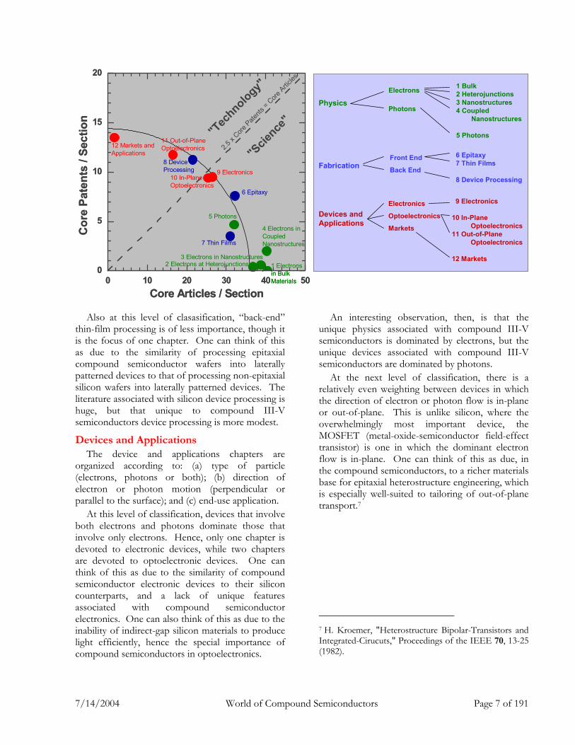
Overall Organization The body of this book is divided into twelve
chapters: five emphasize physics; three emphasize fabrication; and four emphasize devices and applications.
As illustrated in the facing figure, the relative numbers of core articles and patents mapped onto the various chapters depend substantially on their emphases. The physics chapters are weighted towards articles, and can be viewed as having more “science” content. The device and applications chapters are weighted towards patents, and can be viewed as having more “technology” content. The fabrication chapters are evenly weighted, with some aspects (epitaxy and thin films) having more “science” content, and others (device processing) having more “technology” content.
Within each area (physics, fabrication, devices and applications), the chapters are organized according to the following criteria.
Physics The physics chapters are organized according to:
(a) type of particle (electrons or photons); and (b) dimensionality (3D, 2D, 1D or 0D) of the structure.
At the highest level of classification, electrons, the focus of four chapters, are dominant over photons, the focus of only one chapter. One can think of this as due to the stronger Coulomb and exchange interactions between charged Fermions (such as electrons) compared to the weaker interactions between uncharged Bosons (such as photons or phonons). The strength of these interactions has led to a much richer “physics” associated with electrons than with photons or phonons.
Also at this level of classification, photons, the focus of one chapter, are dominant over phonons, the focus of no chapters. One can think of this as due to photons existing independently of (though interacting with) the semiconductor, so that they can be used as inputs and outputs to and from the semiconductor. This is a necessary condition for use in devices, and has led to a much greater importance associated with photons than with phonons.
At the next level of classification, the physics of electrons in compound semiconductors is roughly equally weighted towards 3D electrons in bulk materials (chapter 1), 2D electrons at heterojunctions (chapter 2), 2D and 1D electrons in nanostructures (chapter 3), and electrons in separate but coupled nanostructures (chapter 4). Note that as the dimensionality of the structure decreases, quantum (or wave) effects become progressively more important, but the chapters are not organized around the progressive importance of wave effects.
Also at this level of classification, the physics of photons is weighted (in comparison to electrons) more towards towards 2D and 1D than 3D structures. This can be thought of as due to the much longer wavelengths of photons (0.1-10 µm) than of electrons (0.1-10 nm) -- photons show interesting wave effects in more-easily-fabricated micrometer-scale structures, while electrons only show such effects in less-easily-fabricated nanometer-scale structures.
Fabrication The fabrication chapters are organized according
to: (a) position within the “front-end”-to-“back-end” fabrication flow (from substrates and epitaxy to thin films to thin-film processing); and (b) type of phenomena (surface, thin film or bulk).
At the highest level of classification, “front-end” epitaxy stands out as the single most important fabrication process, even though it is in principle only one of many processes necessary to fabricate a finished device. One can think of this as due to the technical challenges and richness associated with depositing atoms epitaxially (rather than non-epitaxially) as near-perfect thin films on single-crystal surfaces, combined with the importance of these near-perfect thin films to vertically-layered structures that exhibit 2D or 1D physical phenomena.
Hence, two chapters are devoted to epitaxy. One is devoted to those aspects of epitaxy that involve tools (molecular beam epitaxy and organometallic vapor phase epitaxy) and how those tools interact with surfaces. The other is devoted to those aspects of epitaxy that involve materials issues associated with the resulting vertically layered thin films.
7/14/2004 World of Compound Semiconductors Page 7 of 191
Also at this level of clasasification, “back-end” thin-film processing is of less importance, though it is the focus of one chapter. One can think of this as due to the similarity of processing epitaxial compound semiconductor wafers into laterally patterned devices to that of processing non-epitaxial silicon wafers into laterally patterned devices. The literature associated with silicon device processing is huge, but that unique to compound III-V semiconductors device processing is more modest.
Devices and Applications The device and applications chapters are
organized according to: (a) type of particle (electrons, photons or both); (b) direction of electron or photon motion (perpendicular or parallel to the surface); and (c) end-use application.
At this level of classification, devices that involve both electrons and photons dominate those that involve only electrons. Hence, only one chapter is devoted to electronic devices, while two chapters are devoted to optoelectronic devices. One can think of this as due to the similarity of compound semiconductor electronic devices to their silicon counterparts, and a lack of unique features associated with compound semiconductor electronics. One can also think of this as due to the inability of indirect-gap silicon materials to produce light efficiently, hence the special importance of compound semiconductors in optoelectronics.
An interesting observation, then, is that the unique physics associated with compound III-V semiconductors is dominated by electrons, but the unique devices associated with compound III-V semiconductors are dominated by photons.
At the next level of classification, there is a relatively even weighting between devices in which the direction of electron or photon flow is in-plane or out-of-plane. This is unlike silicon, where the overwhelmingly most important device, the MOSFET (metal-oxide-semiconductor field-effect transistor) is one in which the dominant electron flow is in-plane. One can think of this as due, in the compound semiconductors, to a richer materials base for epitaxial heterostructure engineering, which is especially well-suited to tailoring of out-of-plane transport.7
7 H. Kroemer, "Heterostructure Bipolar-Transistors and Integrated-Cirucuts," Proceedings of the IEEE 70, 13-25 (1982).
0 10 20 30 40 500
5
10
15
20
2.5 x
Core P
atents
= Core
Artic
les
12 Markets andApplications
11 Out-of-PlaneOptoelectronics
10 In-PlaneOptoelectronics
9 Electronics8 DeviceProcessing
7 Thin Films
6 Epitaxy
5 Photons
4 Electrons inCoupled Nanostructures
3 Electrons in Nanostructures2 Electrons at Heterojunctions
"Scie
nce"
"Tec
hnology"
Cor
e Pa
tent
s / S
ectio
n
Core Articles / Section
1 Electronsin BulkMaterials
PhysicsElectrons
Photons
1 Bulk2 Heterojunctions3 Nanostructures4 Coupled
Nanostructures
5 Photons
Front End
Back End
6 Epitaxy7 Thin Films
8 Device Processing
Electronics
Optoelectronics
Markets
9 Electronics
10 In-PlaneOptoelectronics
11 Out-of-PlaneOptoelectronics
12 Markets
Fabrication
Devices andApplications
7/14/2004 World of Compound Semiconductors Page 8 of 191
0.4 Table of Contents
0.1 Scope...............................................................2 0.2 Audience and Format.....................................4 0.3 Organization...................................................6 0.4 Table of Contents ...........................................8
1 ELECTRONS IN BULK MATERIALS (255)....... 10 1.1 Electrons in Bonds (27)................................ 12 1.2 Electrons in the Lattice (48)......................... 14 1.3 Electrons and Point Defects (67) ................. 16 1.4 Electrons and Defect Centers (53) ............... 18 1.5 Electron Dynamics (56) ...............................20
2 ELECTRONS AT HETEROJUNCTIONS (192) ..22 2.1 Electron Band Offsets (52)...........................24 2.2 Electrons at Heterojunctions (37)................26 2.3 2D Electron Gases (34).................................30 2.4 2DEGs in Magnetic Fields: Integral
QHE (40) ......................................................32 2.5 2DEGs in Extreme Magnetic Fields:
Fractional QHE (30) Dan Tsui....................34
3 ELECTRONS IN NANOSTRUCTURES (191).....36 3.1 Quantum Wells: Electron Energies (51) .....38 3.2 Quantum Wells: Electron Dynamics (31) ...40 3.3 Quantum Wells: Photons and Electrons
(37) ................................................................42 3.4 Quantum Wires (25) .....................................44 3.5 Quantum Dots (47).......................................46
4 ELECTRONS IN COUPLED
NANOSTRUCTURES (166)..............................48 4.1 Coupled 2D Nanostructures (38) .................50 4.2 Periodic 2D Nanostructures: Energetics
(42) ................................................................52 4.3 Periodic 2D Nanostructures: Dynamics
(38) ................................................................54 4.4 Coupled or Periodic 1D and 0D
Nanostructures (48)......................................56
5 PHOTONS (108).............................................58 5.1 Photons in Bulk Materials (47) ....................60 5.2 Photons in Resonators and Waveguides
(14) ................................................................62 5.3 Photons in Periodic Microstructures (30)....64
6 SUBSTRATES AND EPITAXY (216)..................66 6.1 Molecular Beam Epitaxy (43) ...................... 68 6.2 GaAs Surfaces (48) ....................................... 70 6.3 Non-GaAs Surfaces (33)............................... 72 6.4 Organometallic Vapor Phase Epitaxy
(53)................................................................ 74 6.5 Patterned Surfaces (26) ................................ 76
7 THIN FILMS (147) .........................................78 7.1 Crystallography and Defects (18)................. 80 7.2 Planar Coherency and Semicoherency
(26)................................................................ 84 7.3 Alloy Ordering and Decomposition (17) ..... 86 7.4 Nonplanar Coherency (29)........................... 88 7.5 Nonplanar Semicoherency (43) ................... 90
8 DEVICE PROCESSING (145)...........................92 8.1 Bulk Materials Processing (40).................... 94 8.2 Surface Processing (49)................................ 96 8.3 Thin Films (32) ............................................ 98 8.4 Lithography and Substrate Engineering
(31) ...............................................................100
9 ELECTRONICS (75) ..................................... 102 9.1 MESFETs, MISFETs, HEMTs (41) ..........104 9.2 Diodes, Triodes, Mixers, HBTs (35)..........106
10 IN-PLANE OPTOELECTRONICS (168) ......... 108 10.1 Broad Stripe Double Heterostructure
Lasers (30) ...................................................110 10.2 Gain and Bandwidth Engineering (32) ......112 10.3 Transverse Mode and Polarization
Engineering (18)..........................................114 10.4 Longitudinal Mode and Noise
Engineering (34) .........................................116 10.5 Hybrid and Integrated Devices (26)...........118
11 OUT-OF-PLANE OPTOELECTRONICS
(69,47)......................................................... 120 11.1 Survey of Out-of-Plane Optoelectronics
(0).................................................................122 11.2 LEDs (18) ....................................................124 11.3 VCSELs (28)................................................126 11.4 Detectors and Solar Cells (25).....................128
7/14/2004 World of Compound Semiconductors Page 9 of 191
11.5 Modulators, Gates and Hybrid Devices (24)...............................................................130
12 APPLICATIONS AND MARKETS (11,81) .........132 12.1 Wireless Communications (7) ....................134 12.2 Optical Communications (20) ....................136 12.3 Energy Conversion, Imaging, Sensing
(10)...............................................................138 12.4 Solid State Lighting (11)..............................140
12.5 Materials Processing (14) ........................... 142 12.6 Data Storage (5).......................................... 144
13 INNER-CORE REFERENCES........................146 13.1 Inner-Core Articles by Author.................... 148 13.2 Inner-Core Patents by Author .................... 167 13.3 Inner-Core Articles by Citation Count....... 170 13.4 Inner-Core Patents by Citation Count ....... 189
7/14/2004 World of Compound Semiconductors Page 10 of 191
11 EELLEECCTTRROONNSS IINN BBUULLKK MMAATTEERRIIAALLSS ((220022,,00))
Electrons, Ions and Photons in Electric and Magnetic Fields
Electrons are arguably the most important of the three particles – electrons, photons, ions – involved in compound semiconductor physics. Unlike photons, electrons are charged, hence interact strongly with each other and with electric fields, and can be easily controlled and measured externally. Unlike ions, they have very low mass, and can move macroscopic (mm) distances in the microscopic (ns) times of interest for device applications.
Also, though electrons have both charge and spin, their interactions with electric fields are many orders of magnitude larger than their interactions with magnetic fields. Hence, although there has been some recent interest in magnetic semiconductors, the physics of electrons is dominated by the physics of electrons interacting with electric fields.
In this Chapter, we discuss the physics of electrons in bulk materials, interacting with and through, electric fields. This physics, in turn, can be simplified by three major approximations, around which the sections of this Chapter are organized.
Ion Cores and Valence Electrons The first approximation is that there are two
kinds of electrons in the atoms that make up the semiconductor lattice.
The electrons in completely filled inner shells, combined with the atom nucleus they are tightly bound to, form the inert “ion cores.” These ion cores interact relatively weakly with the other ion cores of the lattice.
The electrons in the partially filled outer shell are relatively weakly bound to the atom’s nucleus, and
form the reactive “valence electrons.” These valence electrons interact relatively strongly with the valence electrons of the other atoms of the lattice. Through these interactions, the valence electrons are responsible for the bonding between the atoms in the lattice. This bonding, discussed in Section 1.1, determines most of the important lattice properties of the semiconductor, such as its energy of formation, its lattice constant at equilibrium and under stress, its vibrational spectrum, and its polarity.
Born-Oppenheimer Approximation The second approximation is that the two
constituents of the semiconductor – the ion cores that form the lattice, and the valence electrons that form the bonds between the ion cores of the lattice – have very different masses and very different response times to perturbations. The ion cores are roughly 1000x? heavier than the valence electrons, and move 1000x more slowly. As a consequence, the lattice can be considered static on the time scale of electron motion and for the purpose of calculating electron energies.
In this Born-Oppenheimer approximation, the valence electrons can be viewed as interacting with themselves against a backdrop of static ion cores. Through these interactions, the electron band structure is derived – the valence band, derived from valence electrons interacting to form bonding orbitals, and the conduction band, derived from valence electrons interacting to form anti-bonding orbitals. This electron band structure and its dependence on composition and strain, are discussed in Section 1.2.
Periodicity and Deviations from Periodicity
7/14/2004 World of Compound Semiconductors Page 11 of 191
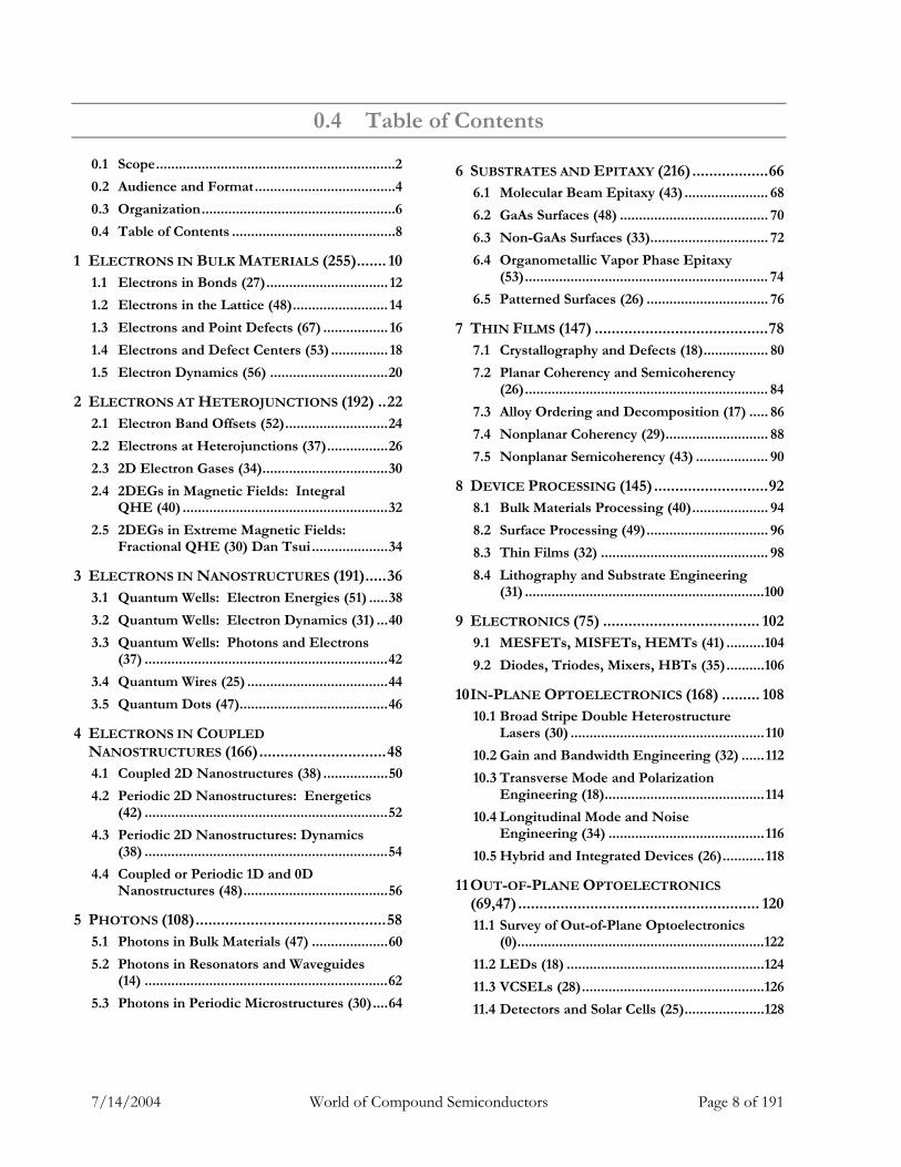
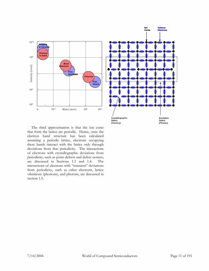
The third approximation is that the ion cores that form the lattice are periodic. Hence, once the electron band structure has been calculated assuming a periodic lattice, electrons occupying these bands interact with the lattice only through deviations from that periodicity. The interactions of electrons with crystallographic deviations from periodicity, such as point defects and defect centers, are discussed in Sections 1.3 and 1.4. The interactions of electrons with “transient” deviations from periodicity, such as other electrons, lattice vibrations (phonons), and photons, are discussed in section 1.5.
0 Mass (amu) 100 10310-6
~~
1012
109
103
Velo
city
(cm
/s)
FreeElectrons
BandElectrons
100
PhotonsIn Vacuum
PhotonsIn Solid
Phonons
FreeAtoms
CrystallographicDefect(Vacancy)
ExcitationDefect(Phonon)
IonCores
ValenceElectrons
0 Mass (amu) 100 10310-6
~~
1012
109
103
Velo
city
(cm
/s)
FreeElectrons
BandElectrons
100
PhotonsIn Vacuum
PhotonsIn Solid
Phonons
FreeAtoms
0 Mass (amu) 100 10310-6
~~ ~~
1012
109
103
Velo
city
(cm
/s)
FreeElectrons
BandElectrons
100
PhotonsIn Vacuum
PhotonsIn Solid
Phonons
FreeAtoms
CrystallographicDefect(Vacancy)
ExcitationDefect(Phonon)
IonCores
ValenceElectrons
7/14/2004 World of Compound Semiconductors Page 12 of 191
1.1 Electrons in Bonds (27)
Bonds and Energies (9) All compound semiconductor phenomena take
place against a backdrop of atoms, and of the bonds between them. These bonds can be understood, to a good approximation, as electrons occupying linear combinations of atomic orbitals. For the simple ANB8-N octet compounds, the relevant orbitals are the one inner-shell s and three outer-shell p orbitals, from which are derived four tetrahedrally oriented sp3 hybrid h orbitals.
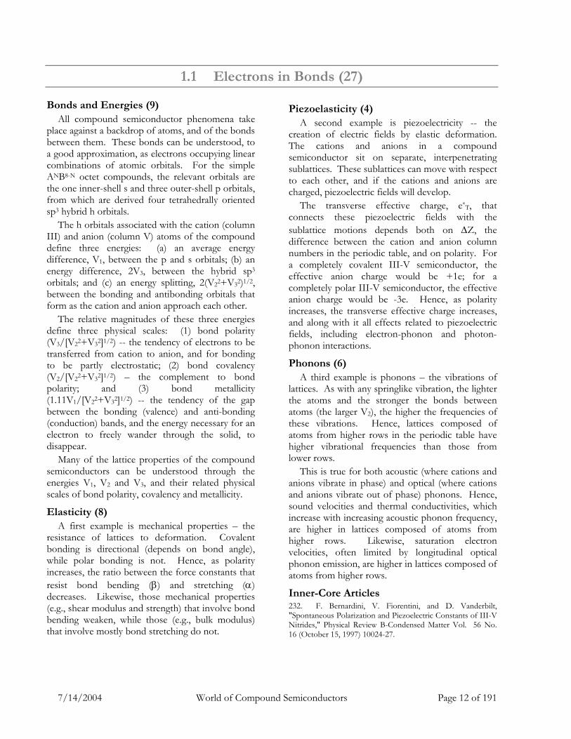
The h orbitals associated with the cation (column III) and anion (column V) atoms of the compound define three energies: (a) an average energy difference, V1, between the p and s orbitals; (b) an energy difference, 2V3, between the hybrid sp3 orbitals; and (c) an energy splitting, 2(V22+V32)1/2, between the bonding and antibonding orbitals that form as the cation and anion approach each other.
The relative magnitudes of these three energies define three physical scales: (1) bond polarity (V3/[V22+V32]1/2) -- the tendency of electrons to be transferred from cation to anion, and for bonding to be partly electrostatic; (2) bond covalency (V2/[V22+V32]1/2) – the complement to bond polarity; and (3) bond metallicity (1.11V1/[V22+V32]1/2) -- the tendency of the gap between the bonding (valence) and anti-bonding (conduction) bands, and the energy necessary for an electron to freely wander through the solid, to disappear.
Many of the lattice properties of the compound semiconductors can be understood through the energies V1, V2 and V3, and their related physical scales of bond polarity, covalency and metallicity.
Elasticity (8) A first example is mechanical properties – the
resistance of lattices to deformation. Covalent bonding is directional (depends on bond angle), while polar bonding is not. Hence, as polarity increases, the ratio between the force constants that resist bond bending (β) and stretching (α) decreases. Likewise, those mechanical properties (e.g., shear modulus and strength) that involve bond bending weaken, while those (e.g., bulk modulus) that involve mostly bond stretching do not.
Piezoelasticity (4) A second example is piezoelectricity -- the
creation of electric fields by elastic deformation. The cations and anions in a compound semiconductor sit on separate, interpenetrating sublattices. These sublattices can move with respect to each other, and if the cations and anions are charged, piezoelectric fields will develop.
The transverse effective charge, e*T, that connects these piezoelectric fields with the sublattice motions depends both on ∆Z, the difference between the cation and anion column numbers in the periodic table, and on polarity. For a completely covalent III-V semiconductor, the effective anion charge would be +1e; for a completely polar III-V semiconductor, the effective anion charge would be -3e. Hence, as polarity increases, the transverse effective charge increases, and along with it all effects related to piezoelectric fields, including electron-phonon and photon-phonon interactions.
Phonons (6) A third example is phonons – the vibrations of
lattices. As with any springlike vibration, the lighter the atoms and the stronger the bonds between atoms (the larger V2), the higher the frequencies of these vibrations. Hence, lattices composed of atoms from higher rows in the periodic table have higher vibrational frequencies than those from lower rows.
This is true for both acoustic (where cations and anions vibrate in phase) and optical (where cations and anions vibrate out of phase) phonons. Hence, sound velocities and thermal conductivities, which increase with increasing acoustic phonon frequency, are higher in lattices composed of atoms from higher rows. Likewise, saturation electron velocities, often limited by longitudinal optical phonon emission, are higher in lattices composed of atoms from higher rows.
Inner-Core Articles 232. F. Bernardini, V. Fiorentini, and D. Vanderbilt, "Spontaneous Polarization and Piezoelectric Constants of III-V Nitrides," Physical Review B-Condensed Matter Vol. 56 No. 16 (October 15, 1997) 10024-27.
7/14/2004 World of Compound Semiconductors Page 13 of 191
222. O.H. Nielsen and R.M. Martin, "Stresses in Semiconductors: Ab Initio Calculations on Si, Ge, and GaAs," Physical Review B-Condensed Matter Vol. 32 No. 6 (September 15, 1985) 3792-805 . 209. W.A. Harrison, "New Tight-Binding Parameters for Covalent Solids Obtained Louie Peripheral States," Physical Review B-Condensed Matter Vol. 24 No. 10 (November 15, 1981) 5835-43.
α
β
-e∗T
+e∗T
V1,anion
V1,cation 2V3
εp,cation
εs,cation
εh,cation εp,anion
εs,anion
εh,anion2(V2
2+V32)1/2
0
10
20
30
40
0.00
0.05
0.10
0.15
0.0 0.2 0.4 0.6 0.8 1.00.0
0.2
0.4
0.6
AlN(W )InN(ZB)
AlN(ZB)
InN(W )InP
GaN(ZB)GaN(W )
ZnTeCdTeZnSeZnS
GaSbAlSb
GaAs
InSb
GaP
InAs
BN
C
Polarity
β / α
SiGe
A com bination of theoretical and experim ental results, afterJ.C. Phillips, Bonds and Bands in Semiconductors (Academic Press,New York, 1973); and A.F. W right, J. Appl. Phys. 82 (2833) 1997.
0
1
2
3AlAs
AlN
CSiGe
ZnSZnO
CdS
CdSe
ZnTe
CdTe
ZnSe
InN
AlPGaAs
GaPGaSbAlSb
InSb InAsGaN
InP BeOBN
II-VIsIII-Vs
Z*
IV-IVs
SiC
A com bination of theoretical and experim ental results, after F. Bernardini, V. Fiorentini and D. Vanderbilt, Phys. Rev. B56, R10 026 (1997); W .A. Harrison, ElectronicStructure and the Properties of Solids (W .H. Freeman, San Francisco, 1980); P.Y. Yu and Manuel Cardona, Fundamentals of Sem iconductors (Springer, Berlin, 1996);M. Hass, Semiconductors and Sem imetals, Vol. 3 (Academ ic, New York, 1967); S.K. Sinha, "Phonons in Sem iconductors," CRC Critical Reviews in Solid StateScience 3, 273-334 (1973); and J.A. Sanjurjo, E. Lopez-Cruz , P. Vogl and M. Cardona, Phys. Rev. B28, 4579 (1983).
GeSn
ZnSe ZnTe CdTe
CdSeCdS
ZnSSi
BP
ZnO
BeOBN
SiC
C
InSb
AlPAlSbGaSb InAs
GaAsInP
GaPInN
GaN
AlN
ν LO (T
Hz)
E LO (e
V)
α
β
-e∗T
+e∗T
V1,anion
V1,cation 2V3
εp,cation
εs,cation
εh,cation εp,anion
εs,anion
εh,anion2(V2
2+V32)1/2
V1,anion
V1,cation 2V3
εp,cation
εs,cation
εh,cation
εp,cation
εs,cation
εh,cation εp,anion
εs,anion
εh,anion
εp,anion
εs,anion
εh,anion2(V2
2+V32)1/2
0
10
20
30
40
0.00
0.05
0.10
0.15
0.0 0.2 0.4 0.6 0.8 1.00.0
0.2
0.4
0.6
AlN(W )InN(ZB)
AlN(ZB)
InN(W )InP
GaN(ZB)GaN(W )
ZnTeCdTeZnSeZnS
GaSbAlSb
GaAs
InSb
GaP
InAs
BN
C
Polarity
β / α
SiGe
A com bination of theoretical and experim ental results, afterJ.C. Phillips, Bonds and Bands in Semiconductors (Academic Press,New York, 1973); and A.F. W right, J. Appl. Phys. 82 (2833) 1997.
0
1
2
3AlAs
AlN
CSiGe
ZnSZnO
CdS
CdSe
ZnTe
CdTe
ZnSe
InN
AlPGaAs
GaPGaSbAlSb
InSb InAsGaN
InP BeOBN
II-VIsIII-Vs
Z*
IV-IVs
SiC
A com bination of theoretical and experim ental results, after F. Bernardini, V. Fiorentini and D. Vanderbilt, Phys. Rev. B56, R10 026 (1997); W .A. Harrison, ElectronicStructure and the Properties of Solids (W .H. Freeman, San Francisco, 1980); P.Y. Yu and Manuel Cardona, Fundamentals of Sem iconductors (Springer, Berlin, 1996);M. Hass, Semiconductors and Sem imetals, Vol. 3 (Academ ic, New York, 1967); S.K. Sinha, "Phonons in Sem iconductors," CRC Critical Reviews in Solid StateScience 3, 273-334 (1973); and J.A. Sanjurjo, E. Lopez-Cruz , P. Vogl and M. Cardona, Phys. Rev. B28, 4579 (1983).
GeSn
ZnSe ZnTe CdTe
CdSeCdS
ZnSSi
BP
ZnO
BeOBN
SiC
C
InSb
AlPAlSbGaSb InAs
GaAsInP
GaPInN
GaN
AlN
ν LO (T
Hz)
E LO (e
V)
7/14/2004 World of Compound Semiconductors Page 14 of 191
1.2 Electrons in the Lattice (48)
Electron Band Calculations (12) As discussed in Section 2.1, the valence electrons
of the lattice reside in the bonding and anti-bonding orbitals between the atoms of the lattice. Because electrons in neighboring bonds interact strongly, it is convenient to describe them as waves distributed through the lattice. How the energies of these waves depend on k-vector (crystal momentum) is the electron band structure.
This band structure is usually calculated using one of three methods: (1) the LCAO (linear combination of atomic orbitals) or tight binding method, which begins with atomic orbitals and combines them into itinerant wavefunctions; (2) the NFE (nearly-free electron) pseudopotential method, which begins with free electrons and perturbs them with pseudopotentials at the ion cores; and (3) the “k dot p” method, which begins with high-symmetry points in k-space, and uses perturbation theory to calculate curvature around those points.
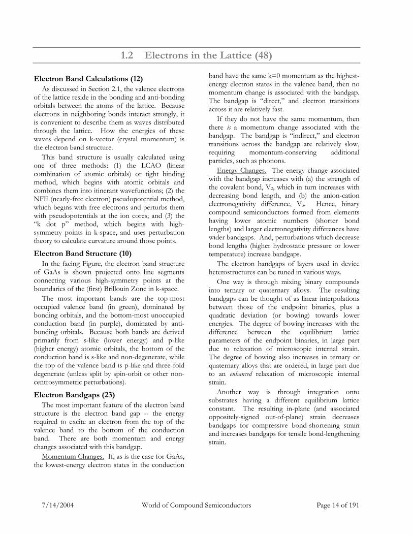
Electron Band Structure (10) In the facing Figure, the electron band structure
of GaAs is shown projected onto line segments connecting various high-symmetry points at the boundaries of the (first) Brillouin Zone in k-space.
The most important bands are the top-most occupied valence band (in green), dominated by bonding orbitals, and the bottom-most unoccupied conduction band (in purple), dominated by anti-bonding orbitals. Because both bands are derived primarily from s-like (lower energy) and p-like (higher energy) atomic orbitals, the bottom of the conduction band is s-like and non-degenerate, while the top of the valence band is p-like and three-fold degenerate (unless split by spin-orbit or other non-centrosymmetric perturbations).
Electron Bandgaps (23) The most important feature of the electron band
structure is the electron band gap -- the energy required to excite an electron from the top of the valence band to the bottom of the conduction band. There are both momentum and energy changes associated with this bandgap.
Momentum Changes. If, as is the case for GaAs, the lowest-energy electron states in the conduction
band have the same k=0 momentum as the highest-energy electron states in the valence band, then no momentum change is associated with the bandgap. The bandgap is “direct,” and electron transitions across it are relatively fast.
If they do not have the same momentum, then there is a momentum change associated with the bandgap. The bandgap is “indirect,” and electron transitions across the bandgap are relatively slow, requiring momentum-conserving additional particles, such as phonons.
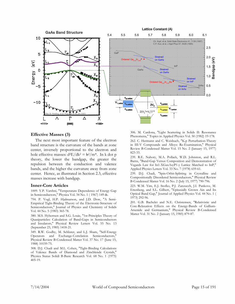
Energy Changes. The energy change associated with the bandgap increases with (a) the strength of the covalent bond, V2, which in turn increases with decreasing bond length, and (b) the anion-cation electronegativity difference, V3. Hence, binary compound semiconductors formed from elements having lower atomic numbers (shorter bond lengths) and larger electronegativity differences have wider bandgaps. And, perturbations which decrease bond lengths (higher hydrostatic pressure or lower temperature) increase bandgaps.
The electron bandgaps of layers used in device heterostructures can be tuned in various ways.
One way is through mixing binary compounds into ternary or quaternary alloys. The resulting bandgaps can be thought of as linear interpolations between those of the endpoint binaries, plus a quadratic deviation (or bowing) towards lower energies. The degree of bowing increases with the difference between the equilibrium lattice parameters of the endpoint binaries, in large part due to relaxation of microscopic internal strain. The degree of bowing also increases in ternary or quaternary alloys that are ordered, in large part due to an enhanced relaxation of microscopic internal strain.
Another way is through integration onto substrates having a different equilibrium lattice constant. The resulting in-plane (and associated oppositely-signed out-of-plane) strain decreases bandgaps for compressive bond-shortening strain and increases bandgaps for tensile bond-lengthening strain.
7/14/2004 World of Compound Semiconductors Page 15 of 191
Effective Masses (3) The next most important feature of the electron
band structure is the curvature of the bands at zone center, inversely proportional to the electron and hole effective masses: d2E/dk2 = h2/m*. In k dot p theory, the lower the bandgap, the greater the repulsion between the conduction and valence bands, and the higher the curvature away from zone center. Hence, as illustrated in Section 2.3, effective masses increase with bandgap.
Inner-Core Articles 1009. Y.P. Varshni, "Temperature Dependence of Energy Gap in Semiconductors," Physica Vol. 34 No. 1 ( 1967) 149-&. 794. P. Vogl, H.P. Hjalmarson, and J.D. Dow, "A Semi-Empirical Tight-Binding Theory of the Electronic-Structure of Semiconductors," Journal of Physics and Chemistry of Solids Vol. 44 No. 5 (1983) 365-78. 380. M.S. Hybertsen and S.G. Louie, "1st-Principles Theory of Quasiparticles: Calculation of Band-Gaps in Semiconductors and Insulators," Physical Review Letters Vol. 55 No. 13 (September 23, 1985) 1418-21. 349. R.W. Godby, M. Schluter, and L.J. Sham, "Self-Energy Operators and Exchange-Correlation Semiconductors," Physical Review B-Condensed Matter Vol. 37 No. 17 (June 15, 1988) 10159-75. 308. D.J. Chadi and M.L. Cohen, "Tight-Binding Calculations of Valence Bands of Diamond and Zincblende Crystals," Physica Status Solidi B-Basic Research Vol. 68 No. 1 (1975) 405-19.
306. M. Cardona, "Light Scattering in Solids II: Resonance Phenomena," Topics in Applied Physics Vol. 50 (1982) 19-178. 262. C. Hermann and C. Weisbuch, "K.p Perturbation-Theory in III-V Compounds and Alloys: Re-Examination," Physical Review B-Condensed Matter Vol. 15 No. 2 (January 15, 1977) 823-33. 239. R.E. Nahory, M.A. Pollack, W.D. Johnston, and R.L. Barns, "Band-Gap Versus Composition and Demonstration of Vegards Law for In1-XGaxAsyP1-y Lattice Matched to InP," Applied Physics Letters Vol. 33 No. 7 (1978) 659-61. 239. D.J. Chadi, "Spin-Orbit-Splitting in Crystalline and Compositionally Disordered Semiconductors," Physical Review B-Condensed Matter Vol. 16 No. 2 (July 15, 1977) 790-796. 223. W.M. Yim, E.J. Stofko, P.J. Zanzucch, J.I. Pankove, M. Ettenberg, and S.L. Gilbert, "Epitaxially Grown Ain and Its Optical Band Gap," Journal of Applied Physics Vol. 44 No. 1 ( 1973) 292-96. 201. G.B. Bachelet and N.E. Christensen, "Relativistic and Core-Relaxation Effects on the Energy-Bands of Gallium-Arsenide and Germanium," Physical Review B-Condensed Matter Vol. 31 No. 2 (January 15, 1985) 879-87.
5.4 5.5 5.6 5.7 5.8 5.9 6.0 6.1
0.0
0.5
1.0
1.5
2.0
2.5
Strainedon InAs
Strainedon InP
Strainedon GaAs
Strainedon GaAs
Ordered Ga0.47
In0.53
As
Ordered Ga0.52
In0.48
P
InAs
InPGaAs
Lattice Constant (A)
GaP
Ban
dgap
(eV)
Ch. Kopf, et al, Solid State Electronics 41, 1139 (1997)C.P. Kuo, et al, J Appl Phys 57, 5428 (1985)
<111> [000] <100>
V1,anion
V1,cation2V3
εp,cation
εs,cation
εh,cation εp,anion
εs,anion
εh,anion2(V2
2+V32)1/2
GaAs Band Structure
After M. Rohlfing, et al, Phys Rev B 48, 24 (1993)
5.4 5.5 5.6 5.7 5.8 5.9 6.0 6.1
0.0
0.5
1.0
1.5
2.0
2.5
Strainedon InAs
Strainedon InP
Strainedon GaAs
Strainedon GaAs
Ordered Ga0.47
In0.53
As
Ordered Ga0.52
In0.48
P
InAs
InPGaAs
Lattice Constant (A)
GaP
Ban
dgap
(eV)
Ch. Kopf, et al, Solid State Electronics 41, 1139 (1997)C.P. Kuo, et al, J Appl Phys 57, 5428 (1985)
<111> [000] <100>
V1,anion
V1,cation2V3
εp,cation
εs,cation
εh,cation εp,anion
εs,anion
εh,anion2(V2
2+V32)1/2
V1,anion
V1,cation2V3
εp,cation
εs,cation
εh,cation
εp,cation
εs,cation
εh,cation εp,anion
εs,anion
εh,anion
εp,anion
εs,anion
εh,anion2(V2
2+V32)1/2
GaAs Band Structure
After M. Rohlfing, et al, Phys Rev B 48, 24 (1993)
7/14/2004 World of Compound Semiconductors Page 16 of 191
1.3 Electrons and Point Defects (67)
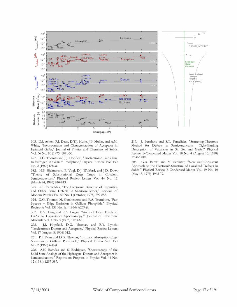
Point Defects (7) As discussed in Section 8.2, all semiconductor
lattices have point defects. Some are “intrinsic” defects native to the pure semiconductor (e.g., vacancies, interstitials, antisites). Some are “extrinsic” defects due to foreign impurity atoms accidentally or intentionally placed in the lattice (e.g., substitutionals, interstitials).
Point defects can exist in multiple charge states, depending on the Fermi level (or “electrochemical potential”) for electrons in the lattice. When the Fermi level is low, the defect donates electrons to the lattice; when high, it accepts them from the lattice. In turn, the Fermi level is determined by the charge-state occupation statistics of the aggregate point-defect population, in a self-consistent manner.
“Shallow” Extended-Wave-Function Levels (15)
The simplest case is a substitutional impurity with one extra electron or hole beyond that necessary to satisfy local bonding requirements. The electron or hole is donated by, but retains a weak Coulomb attraction to, the impurity. This situation is analogous to that of the hydrogen atom, except that the electron or hole mass is determined by the band structure, and the Coulomb attraction is reduced (screened) by the dielectric constant, of the semiconductor. The energy needed to ionize the electron or hole from the impurity is that of the hydrogen atom, multiplied by the effective mass, divided by the dielectric constant squared.
As discussed in Sections 2.5 and 6.1, effective masses increase, and dielectric constants decrease, with bandgap; hence ionization energies increase roughly as bandgap cubed. Hence, wider-bandgap semiconductors are more difficult to “dope” than narrower-bandgap semiconductors. And, since holes are heavier than electrons, p-type doping is more difficult than n-type doping. Note that ionization energies must be less than kT ~ 25meV for significant ionization, or “activation,” of donors or acceptors at room temperature. Hence, semiconductors with bandgaps wider than 2.5-3.0eV are difficult to dope n-type, while those with bandgaps wider than 1.0-1.5eV are difficult to dope p-type.
“Deep” Localized-Wave-Function Levels (23)
In some cases, the electron or hole interacts as (or more) strongly with the localized central-cell, as with the delocalized Coulomb, potentials associated with the point defect -- particularly if there are large local strains. Then, chemical shifts, or central-cell corrections, usually (but not always) cause the electron or hole to be more deeply bound than the hydrogenic effective-mass model would predict.
Because these “deep” levels are localized, and interact relatively weakly with delocalized lattice electrons, they change charge states sluggishly, causing slow, thermally activated capacitance transients in Fermi-level-sweeping experiments. Also, because these deep levels are within the gap, recombination of electrons and holes, where one or both reside on a single (or neighboring) point defect, manifests itself as normally-unobserved within-bandgap luminescence.
Excitons (22) Electrons and holes can bind not only to point
defects, but to each other. The result is a localized electron-hole pair, or exciton. The ionization energy of excitons is slightly less than that of donors and acceptors, because of its “reduced” effective mass. When an electron and hole pair in an exciton recombine, the energy of the resulting photon is reduced from the band-edge by the exciton ionization energy.
Note that the central-cell potentials that give rise to deep levels can also capture and bind excitons. When an electron-hole pair in such a bound exciton recombine, the photon energy is reduced even further from the band-edge by the binding energy of the exciton to the point defect. A famous example is GaP:NP, in which excitons are bound to the localized strain field associated with NP, enabling red and yellow photoluminescence despite a normally low recombination rate associated with indirect-gap GaP.
Inner-Core Articles 1549. J.M. Luttinger and W. Kohn, "Motion of Electrons and Holes in Perturbed Periodic Fields," Physical Review Vol. 97 (1955) 869.
7/14/2004 World of Compound Semiconductors Page 17 of 191
503. D.J. Ashen, P.J. Dean, D.T.J. Hurle, J.B. Mullin, and A.M. White, "Incorporation and Characterization of Acceptors in Epitaxial GaAs," Journal of Physics and Chemistry of Solids Vol. 36 No. 10 (1975) 1041-53. 427. D.G. Thomas and J.J. Hopfield, "Isoelectronic Traps Due to Nitrogen in Gallium Phosphide," Physical Review Vol. 150 No. 2 (1966) 680-&. 382. H.P. Hjalmarson, P. Vogl, D.J. Wolford, and J.D. Dow, "Theory of Substitutional Deep Traps in Covalent Semiconductors," Physical Review Letters Vol. 44 No. 12 (March 24, 1980) 810-813. 375. S.T. Pantelides, "The Electronic Structure of Impurities and Other Point Defects in Semiconductors," Reviews of Modern Physics Vol. 50 No. 4 (October, 1978) 797-858. 324. D.G. Thomas, M. Gershenzon, and F.A. Trumbore, "Pair Spectra + Edge Emission in Gallium Phosphide," Physical Review A Vol. 133 No. 1a ( 1964) A269-&. 307. D.V. Lang and R.A. Logan, "Study of Deep Levels in GaAs by Capacitance Spectroscopy," Journal of Electronic Materials Vol. 4 No. 5 (1975) 1053-66. 275. J.J. Hopfield, D.G. Thomas, and R.T. Lynch, "Isoelectronic Donors and Acceptors," Physical Review Letters Vol. 17 (August 8, 1966) 312. 261. P.J. Dean and D.G. Thomas, "Intrinsic Absorption-Edge Spectrum of Gallium Phosphide," Physical Review Vol. 150 No. 2 (1966) 690-&. 228. A.K. Ramdas and S. Rodriguez, "Spectroscopy of the Solid-State Analogs of the Hydrogen- Donors and Acceptors in Semiconductors," Reports on Progress in Physics Vol. 44 No. 12 (1981) 1297-387.
217. J. Bernholc and S.T. Pantelides, "Scattering-Theoretic Method for Defects in Semiconductors Tight-Binding Description of Vacancies in Si, Ge, and GaAs," Physical Review B-Condensed Matter Vol. 18 No. 4 (August 15, 1978) 1780-1789. 208. G.A. Baraff and M. Schluter, "New Self-Consistent Approach to the Electronic-Structure of Localized Defects in Solids," Physical Review B-Condensed Matter Vol. 19 No. 10 (May 15, 1979) 4965-79.
10-2
10-1
100
10-3
10-2
10-1
100
10-3
10-2
10-1
100
10-3
10-2
10-1
100
0 1 2 3 4 5 6 705
101520
InN
InSb
InAs
Ge GaSb
Si InPGaAs
CdTeAlAs
GaP
CdS ZnSe ZnS
GaN AlN
Die
lect
ricco
nsta
nt (ε
)
Bandgap (eV)
C
Excitons
Holes
ZnSe
ZnS
Effe
ctiv
e
Mas
s (m
* /mo)
C AlNGaNCdS
GaPAlAs
GaAsInP
SiCdTeInN
GaSb
Ge
InSb
InAs
E lectrons
300KGaSb
Ge
GaP:Ge
GaSb:TeGaSb:Se
GaAs
GaAs:Te
GaP:O
GaN:SiCdS
ε Ioni
zatio
n (eV)
CGaPAlAsInP
Si
InN
GaSb:S
InAsInSb
Donors
Ge
InNInSb
InP
InP:HgInP:Mn GaAs:Sn
GaPGaP:Si/Ge GaN
GaN:Mg
ε ioni
zatio
n (eV)
Acceptors C:BGaN:CGaP:Cr
AlAsGaAsSi
GaSbInAs
300K
300K
Excitons
ε ioni
zatio
n (eV)
CGaNGaPAlAs
GaAs
InP
GaSb
SiInN
GeInAsInSb
Ge
CGaN
GaPAlAsGaAsInPSi
InNGaSbInSb
InAs
4s3s
2s
1s
εionization
= [(m*/mo)/ε2]13.6eV
LocalizedCorePotential
Non-LocalizedCoulombPotentialV = e2/(4πεε
οr)
7/14/2004 World of Compound Semiconductors Page 18 of 191
1.4 Electrons and Defect Centers (53)
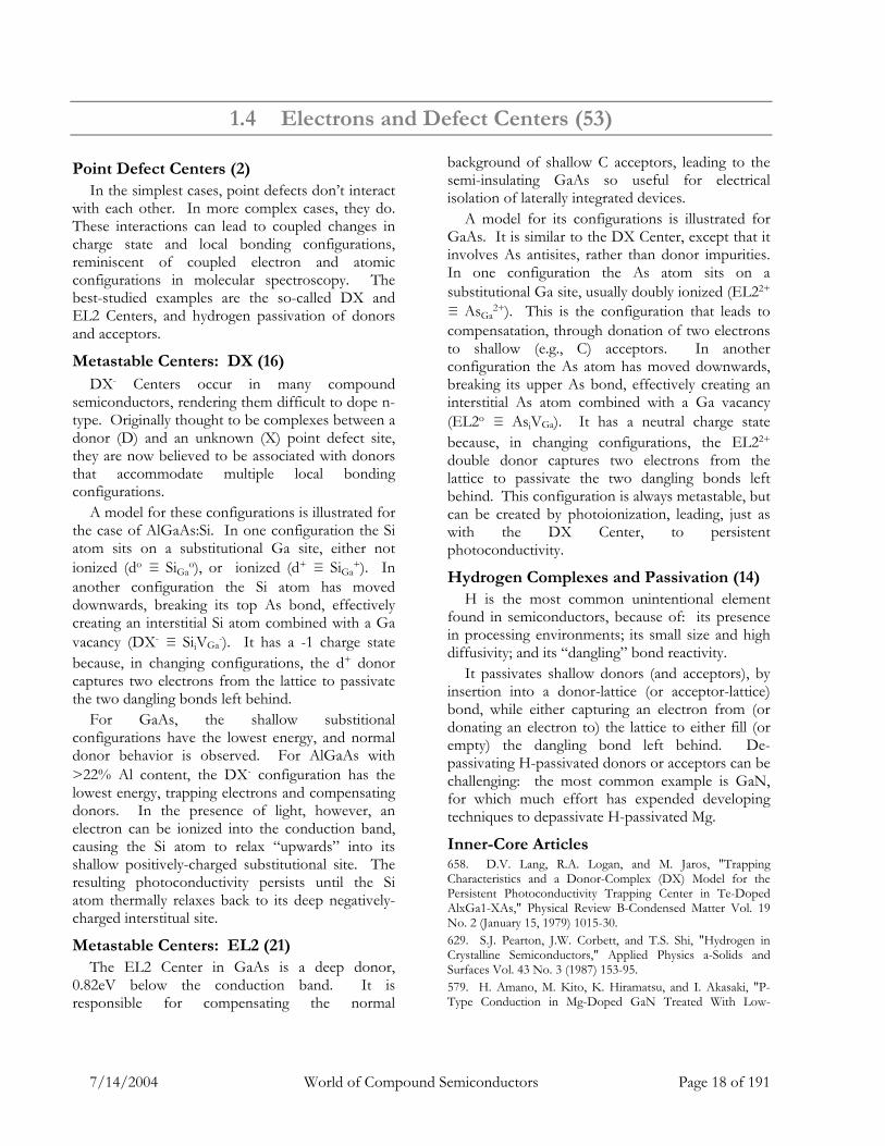
Point Defect Centers (2) In the simplest cases, point defects don’t interact
with each other. In more complex cases, they do. These interactions can lead to coupled changes in charge state and local bonding configurations, reminiscent of coupled electron and atomic configurations in molecular spectroscopy. The best-studied examples are the so-called DX and EL2 Centers, and hydrogen passivation of donors and acceptors.
Metastable Centers: DX (16) DX- Centers occur in many compound
semiconductors, rendering them difficult to dope n-type. Originally thought to be complexes between a donor (D) and an unknown (X) point defect site, they are now believed to be associated with donors that accommodate multiple local bonding configurations.
A model for these configurations is illustrated for the case of AlGaAs:Si. In one configuration the Si atom sits on a substitutional Ga site, either not ionized (do ≡ SiGa
o), or ionized (d+ ≡ SiGa+). In
another configuration the Si atom has moved downwards, breaking its top As bond, effectively creating an interstitial Si atom combined with a Ga vacancy (DX- ≡ SiiVGa-). It has a -1 charge state because, in changing configurations, the d+ donor captures two electrons from the lattice to passivate the two dangling bonds left behind.
For GaAs, the shallow substitional configurations have the lowest energy, and normal donor behavior is observed. For AlGaAs with >22% Al content, the DX- configuration has the lowest energy, trapping electrons and compensating donors. In the presence of light, however, an electron can be ionized into the conduction band, causing the Si atom to relax “upwards” into its shallow positively-charged substitutional site. The resulting photoconductivity persists until the Si atom thermally relaxes back to its deep negatively-charged interstitual site.
Metastable Centers: EL2 (21) The EL2 Center in GaAs is a deep donor,
0.82eV below the conduction band. It is responsible for compensating the normal
background of shallow C acceptors, leading to the semi-insulating GaAs so useful for electrical isolation of laterally integrated devices.
A model for its configurations is illustrated for GaAs. It is similar to the DX Center, except that it involves As antisites, rather than donor impurities. In one configuration the As atom sits on a substitutional Ga site, usually doubly ionized (EL22+ ≡ AsGa
2+). This is the configuration that leads to compensatation, through donation of two electrons to shallow (e.g., C) acceptors. In another configuration the As atom has moved downwards, breaking its upper As bond, effectively creating an interstitial As atom combined with a Ga vacancy (EL2o ≡ AsiVGa). It has a neutral charge state because, in changing configurations, the EL22+ double donor captures two electrons from the lattice to passivate the two dangling bonds left behind. This configuration is always metastable, but can be created by photoionization, leading, just as with the DX Center, to persistent photoconductivity.
Hydrogen Complexes and Passivation (14) H is the most common unintentional element
found in semiconductors, because of: its presence in processing environments; its small size and high diffusivity; and its “dangling” bond reactivity.
It passivates shallow donors (and acceptors), by insertion into a donor-lattice (or acceptor-lattice) bond, while either capturing an electron from (or donating an electron to) the lattice to either fill (or empty) the dangling bond left behind. De-passivating H-passivated donors or acceptors can be challenging: the most common example is GaN, for which much effort has expended developing techniques to depassivate H-passivated Mg.
Inner-Core Articles 658. D.V. Lang, R.A. Logan, and M. Jaros, "Trapping Characteristics and a Donor-Complex (DX) Model for the Persistent Photoconductivity Trapping Center in Te-Doped AlxGa1-XAs," Physical Review B-Condensed Matter Vol. 19 No. 2 (January 15, 1979) 1015-30. 629. S.J. Pearton, J.W. Corbett, and T.S. Shi, "Hydrogen in Crystalline Semiconductors," Applied Physics a-Solids and Surfaces Vol. 43 No. 3 (1987) 153-95. 579. H. Amano, M. Kito, K. Hiramatsu, and I. Akasaki, "P-Type Conduction in Mg-Doped GaN Treated With Low-
7/14/2004 World of Compound Semiconductors Page 19 of 191
Energy Electron-Beam Irradiation (Leebi)," Japanese Journal of Applied Physics Part 2-Letters Vol. 28 No. 12 (1989) L2112-L2114. 542. G.M. Martin, A. Mitonneau, and A. Mircea, "Electron Traps in Bulk and Epitaxial GaAs Crystals," Electronics Letters Vol. 13 No. 7 (1977) 191-93. 524. P.M. Mooney, "Deep Donor Levels (Dx Centers) in III-V Semiconductors," Journal of Applied Physics Vol. 67 No. 3 (February 1, 1990) R1-R26. 463. D.J. Chadi and K.J. Chang, "Theory of the Atomic and Electronic-Structure of Dx Centers in GaAs and AlxGa1-XAs Alloys," Physical Review Letters Vol. 61 No. 7 (August 15, 1988) 873-76 . 422. D.V. Lang and R.A. Logan, "Large-Lattice-Relaxation Model for Persistent Photoconductivity in Compound Semiconductors," Physical Review Letters Vol. 39 No. 10 ( September 5, 1977) 635-39. 404. G.M. Martin, "Optical Assessment of the Main Electron Trap in Bulk Semi-Insulating GaAs," Applied Physics Letters Vol. 39 No. 9 (1981) 747-48. 366. D.J. Chadi and K.J. Chang, "Energetics of Dx-Center Formation in GaAs and AlxGa1-XAs Alloys," Physical Review B-Condensed Matter Vol. 39 No. 14 (May 15, 1989) 10063-74. 328. S. Nakamura, N. Iwasa, M. Senoh, and T. Mukai, "Hole Compensation Mechanism of P-Type GaN Films," Japanese Journal of Applied Physics Part 1-Regular Papers Notes & Review Papers Vol. 31 No. 5a (May, 1992) 1258-66. 314. N. Chand, T. Henderson, J. Klem, W.T. Masselink, R. Fischer, Y.C. Chang, and H. Morkoc, "Comprehensive Analysis of Si-Doped AlxGa1-XAs (x=0 to 1): Theory and Experiments," Physical Review B-Condensed Matter Vol. 30 No. 8 (October 15, 1984) 4481-92.
276. E.W. Williams, "Evidence for Self-Activated Luminescence in Gaas - Gallium Vacancy-Donor Center," Physical Review Vol. 168 No. 3 ( 1968) 922-&. 247. J. Lagowski, H.C. Gatos, J.M. Parsey, K. Wada, M. Kaminska, and W. Walukiewicz, "Origin of the 0.82-Ev Electron Trap in GaAs and Its Annihilation by Shallow Donors," Applied Physics Letters Vol. 40 No. 4 (1982) 342-44. 238. D.J. Chadi and K.J. Chang, "Metastability of the Isolated Arsenic-Antisite Defect in GaAs," Physical Review Letters Vol. 60 No. 21 (May 23, 1988) 2187-90. 234. R.J. Nelson, "Long-Lifetime Photoconductivity Effect in N-Type Gaaias," Applied Physics Letters Vol. 31 No. 5 (1977) 351-53. 233. J. Dabrowski and M. Scheffler, "Theoretical Evidence for an Optically Inducible Structural Transition of the Isolated As Antisite in GaAs - Identification and Explanation of EL2," Physical Review Letters Vol. 60 No. 21 (1988) 2183-86. 230. M. Mizuta, M. Tachikawa, H. Kukimoto, and S. Minomura, "Direct Evidence for the DX Center Being a Substitutional Donor in AlGaAs Alloy System," Japanese Journal of Applied Physics Part 2-Letters Vol. 24 No. 2 (1985) L143-L146. 219. A. Mitonneau, G.M. Martin, and A. Mircea, "Hole Traps in Bulk and Epitaxial GaAs Crystals," Electronics Letters Vol. 13 No. 22 (1977) 666-68.
DX Center
EL2 Center
H + Donor Complex
After DJ Chadi and KJ Chang, Phys Rev B39, 10063 (1989).
After DJ Chadi and KJ Chang, Phys Rev Lett 60, 2187 (1988).
H + Acceptor Complex
AsGa+/++ AsiVGa
o
do/+ = SiGao/+ DX- = SiiVGa
-
BeGa-/o BeiHGa
SiGao/+ SiGaHi
After Vincent and Bois, J Appl Phys 53, 3643 (1982).
7/14/2004 World of Compound Semiconductors Page 20 of 191
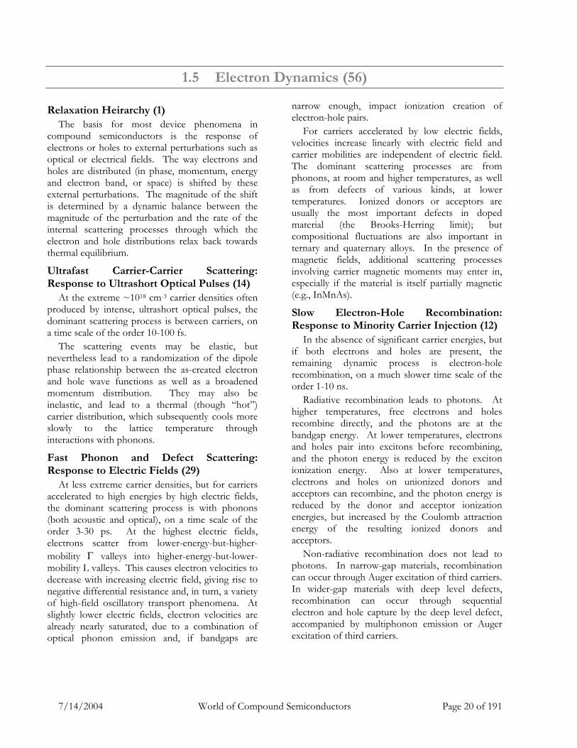
1.5 Electron Dynamics (56)
Relaxation Heirarchy (1) The basis for most device phenomena in
compound semiconductors is the response of electrons or holes to external perturbations such as optical or electrical fields. The way electrons and holes are distributed (in phase, momentum, energy and electron band, or space) is shifted by these external perturbations. The magnitude of the shift is determined by a dynamic balance between the magnitude of the perturbation and the rate of the internal scattering processes through which the electron and hole distributions relax back towards thermal equilibrium.
Ultrafast Carrier-Carrier Scattering: Response to Ultrashort Optical Pulses (14)
At the extreme ~1018 cm-3 carrier densities often produced by intense, ultrashort optical pulses, the dominant scattering process is between carriers, on a time scale of the order 10-100 fs.
The scattering events may be elastic, but nevertheless lead to a randomization of the dipole phase relationship between the as-created electron and hole wave functions as well as a broadened momentum distribution. They may also be inelastic, and lead to a thermal (though “hot”) carrier distribution, which subsequently cools more slowly to the lattice temperature through interactions with phonons.
Fast Phonon and Defect Scattering: Response to Electric Fields (29)
At less extreme carrier densities, but for carriers accelerated to high energies by high electric fields, the dominant scattering process is with phonons (both acoustic and optical), on a time scale of the order 3-30 ps. At the highest electric fields, electrons scatter from lower-energy-but-higher-mobility Γ valleys into higher-energy-but-lower-mobility L valleys. This causes electron velocities to decrease with increasing electric field, giving rise to negative differential resistance and, in turn, a variety of high-field oscillatory transport phenomena. At slightly lower electric fields, electron velocities are already nearly saturated, due to a combination of optical phonon emission and, if bandgaps are
narrow enough, impact ionization creation of electron-hole pairs.
For carriers accelerated by low electric fields, velocities increase linearly with electric field and carrier mobilities are independent of electric field. The dominant scattering processes are from phonons, at room and higher temperatures, as well as from defects of various kinds, at lower temperatures. Ionized donors or acceptors are usually the most important defects in doped material (the Brooks-Herring limit); but compositional fluctuations are also important in ternary and quaternary alloys. In the presence of magnetic fields, additional scattering processes involving carrier magnetic moments may enter in, especially if the material is itself partially magnetic (e.g., InMnAs).
Slow Electron-Hole Recombination: Response to Minority Carrier Injection (12)
In the absence of significant carrier energies, but if both electrons and holes are present, the remaining dynamic process is electron-hole recombination, on a much slower time scale of the order 1-10 ns.
Radiative recombination leads to photons. At higher temperatures, free electrons and holes recombine directly, and the photons are at the bandgap energy. At lower temperatures, electrons and holes pair into excitons before recombining, and the photon energy is reduced by the exciton ionization energy. Also at lower temperatures, electrons and holes on unionized donors and acceptors can recombine, and the photon energy is reduced by the donor and acceptor ionization energies, but increased by the Coulomb attraction energy of the resulting ionized donors and acceptors.
Non-radiative recombination does not lead to photons. In narrow-gap materials, recombination can occur through Auger excitation of third carriers. In wider-gap materials with deep level defects, recombination can occur through sequential electron and hole capture by the deep level defect, accompanied by multiphonon emission or Auger excitation of third carriers.
7/14/2004 World of Compound Semiconductors Page 21 of 191
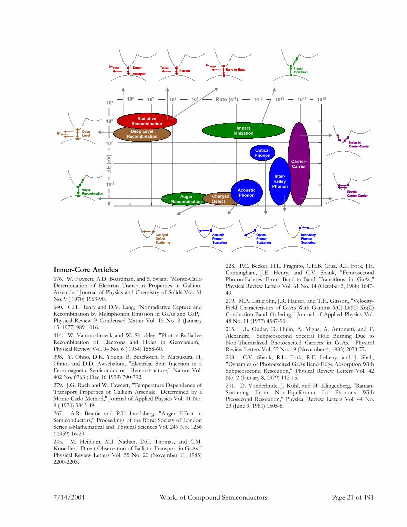
Inner-Core Articles 676. W. Fawcett, A.D. Boardman, and S. Swain, "Monte-Carlo Determination of Electron Transport Properties in Gallium Arsenide," Journal of Physics and Chemistry of Solids Vol. 31 No. 9 ( 1970) 1963-90. 640. C.H. Henry and D.V. Lang, "Nonradiative Capture and Recombination by Multiphonon Emission in GaAs and GaP," Physical Review B-Condensed Matter Vol. 15 No. 2 (January 15, 1977) 989-1016. 414. W. Vanroosbroeck and W. Shockley, "Photon-Radiative Recombination of Electrons and Holes in Germanium," Physical Review Vol. 94 No. 6 ( 1954) 1558-60. 398. Y. Ohno, D.K. Young, B. Beschoten, F. Matsukura, H. Ohno, and D.D. Awschalom, "Electrical Spin Injection in a Ferromagnetic Semiconductor Heterostructure," Nature Vol. 402 No. 6763 ( Dec 16 1999) 790-792. 279. J.G. Ruch and W. Fawcett, "Temperature Dependence of Transport Properties of Gallium Arsenide Determined by a Monte-Carlo Method," Journal of Applied Physics Vol. 41 No. 9 ( 1970) 3843-49. 267. A.R. Beattie and P.T. Landsberg, "Auger Effect in Semiconductors," Proceedings of the Royal Society of London Series a-Mathematical and Physical Sciences Vol. 249 No. 1256 ( 1959) 16-29. 245. M. Heiblum, M.I. Nathan, D.C. Thomas, and C.M. Knoedler, "Direct Observation of Ballistic Transport in GaAs," Physical Review Letters Vol. 55 No. 20 (November 11, 1985) 2200-2203.
228. P.C. Becker, H.L. Fragnito, C.H.B. Cruz, R.L. Fork, J.E. Cunningham, J.E. Henry, and C.V. Shank, "Femtosecond Photon-Echoes From Band-to-Band Transitions in GaAs," Physical Review Letters Vol. 61 No. 14 (October 3, 1988) 1647-49. 219. M.A. Littlejohn, J.R. Hauser, and T.H. Glisson, "Velocity-Field Characteristics of GaAs With Gamma-6(C)-L6(C)-X6(C) Conduction-Band Ordering," Journal of Applied Physics Vol. 48 No. 11 (1977) 4587-90. 215. J.L. Oudar, D. Hulin, A. Migus, A. Antonetti, and F. Alexandre, "Subpicosecond Spectral Hole Burning Due to Non-Thermalized Photoexcited Carriers in GaAs," Physical Review Letters Vol. 55 No. 19 (November 4, 1985) 2074-77. 208. C.V. Shank, R.L. Fork, R.F. Leheny, and J. Shah, "Dynamics of Photoexcited GaAs Band-Edge Absorption With Subpicosecond Resolution," Physical Review Letters Vol. 42 No. 2 (January 8, 1979) 112-15. 201. D. Vonderlinde, J. Kuhl, and H. Klingenberg, "Raman-Scattering From Non-Equilibrium Lo Phonons With Picosecond Resolution," Physical Review Letters Vol. 44 No. 23 (June 9, 1980) 1505-8.
AugerRecombination
ChargedDefect
DeepLevel
hωphonon
AugerRecombination Elastic
Carrier-Carrier
InelasticCarrier-Carrier
ImpactIonization
IntervalleyPhononScattering
Band-to-Bandhνphoton
ExcitonhνphotonDonor
Acceptor
hνphoton
OpticalPhononScattering
AcousticPhononScattering
ChargedDefectScattering
Carrier-Carrier
ImpactIonization
OpticalPhonon
AcousticPhonon
Deep LevelRecombination
RadiativeRecombination
Inter-valley
Phonon
107 108 Rate (s-1) 1012 1013 1014 1015106 109101
100
10-3
0
∆E
(eV)
~~
10-1
AugerRecombination
ChargedDefect
DeepLevel
hωphononDeepLevel
hωphonon
AugerRecombinationAugerRecombination Elastic
Carrier-CarrierElasticCarrier-Carrier
InelasticCarrier-CarrierInelasticCarrier-Carrier
ImpactIonizationImpactIonization
IntervalleyPhononScattering
IntervalleyPhononScattering
Band-to-Bandhνphoton
Band-to-Bandhνphoton
Excitonhνphoton
ExcitonhνphotonDonor
Acceptor
hνphoton Donor
Acceptor
hνphoton
OpticalPhononScattering
OpticalPhononScattering
AcousticPhononScattering
AcousticPhononScattering
ChargedDefectScattering
ChargedDefectScattering
Carrier-Carrier
ImpactIonization
OpticalPhonon
AcousticPhonon
Deep LevelRecombination
RadiativeRecombination
Inter-valley
Phonon
107 108 Rate (s-1) 1012 1013 1014 1015106 109107 108 Rate (s-1) 1012 1013 1014 1015106 109101
100
10-3
0
∆E
(eV)
~~
10-1
101
100
10-3
0
∆E
(eV)
~~~~
10-1
7/14/2004 World of Compound Semiconductors Page 22 of 191
22 EELLEECCTTRROONNSS AATT HHEETTEERROOJJUUNNCCTTIIOONNSS ((222288)) One- and Many-Electron Phenomena in Heterojunctions
Quantum well effects are also included, provided only the lowest energy level is involved, since then it is essentially a single heterojunction phenomena – there is no difference between a square or deep triangular well

7/14/2004 World of Compound Semiconductors Page 23 of 191

7/14/2004 World of Compound Semiconductors Page 24 of 191
2.1 Semiconductor-Semiconductor Junctions: Band Offsets (52)
Survey Band gaps vs band offsets Absolute band-edge reference energies Valence band offsets and inferred conduction band offsets (or vice versa) Bulk vs interface contributions If bulk dominated, one expects transitivity and commutativity; if interface dominated, one doesn’t expect
transitivity or commutativity
Perfect Interfaces and Pseudomorphic Films (13) 2.1.0.1 Basic physics
2.1.0.2 Early theories
Electron affinity rule for conduction band referencing (Anderson) – the energy gained by adding an additional electron to an atom or solid Common anion rule for conduction band referencing plus d-orbital corrections Natural band lineups using free atom referencing (Harrison) Frensley-Kroemer model Neutrality levels (Tersoff) 2.1.0.3 Model solid density functional theories
Basic theory Spin-orbit splittings Band edge deformation potentials for strained films
Imperfect Interfaces and Strained Films (6) 2.1.0.4 Interface dipoles
2.1.0.5 Dielectrics
2.1.0.6 Free surfaces
2.1.0.7 Piezoelectric effects
Measurement Techniques and Results (12) 2.1.0.8 XPS and CV measurements
2.1.0.9 Quantum well PLE measurements
2.1.0.10 Absolute measurements of x
2.1.0.11 Survey of Binary and Alloy Interfaces
InGaAs and InAlAs on InP InGaP/GaAs AlAs/GaAs Antimonides Nitrides
7/14/2004 World of Compound Semiconductors Page 25 of 191
Schottky Barriers (17) 2.1.0.12 Theory
2.1.0.13 Measurements
Inner-Core Articles 704. W.E. Spicer, P.W. Chye, P.R. Skeath, C.Y. Su, and I. Lindau, "New and Unified Model for Schottky-Barrier and III-V Interface States Formation," Journal of Vacuum Science & Technology Vol. 16 No. 5 (1979) 1422-33. 575. J. Tersoff, "Schottky-Barrier Heights and the Continuum of Gap States," Physical Review Letters Vol. 52 No. 6 (February 6, 1984) 465-68. 570. C.G. Vandewalle, "Band Lineups and Deformation Potentials in the Model-Solid Theory," Physical Review B-Condensed Matter Vol. 39 No. 3 (January 15, 1989) 1871-83. 541. R.C. Miller, D.A. Kleinman, and A.C. Gossard, "Energy-Gap Discontinuities and Effective Masses for GaAs-AlxGa1-XAs Quantum Wells," Physical Review B-Condensed Matter Vol. 29 No. 12 (June 15, 1984) 7085-87. 539. W.E. Spicer, I. Lindau, P. Skeath, C.Y. Su, and P.W. Chye, "Unified Mechanism for Schottky-Barrier Formation and III-V-Oxide Interface States," Physical Review Letters Vol. 44 No. 6 (February 11, 1980) 420-423. W.E. Spicer, I. Lindau, P. Skeath, and C.Y. Su, "Unified Defect Model and Beyond," Journal of Vacuum Science & Technology Vol. 17 No. 5 (1980) 1019-27. 392. J. Tersoff, "Theory of Semiconductor Heterojunctions: the Role of Dipoles," Physical Review B-Condensed Matter Vol. 30 No. 8 (October 15, 1984) 4874-77. 382. W.A. Harrison, "Elementary Theory of Heterojunctions," Journal of Vacuum Science & Technology Vol. 14 No. 4 (1977) 1016-21. 319. M. Cardona and N.E. Christensen, "Acoustic Deformation Potentials and Heterostructure Band Offsets in Semiconductors," Physical Review B-Condensed Matter Vol. 35 No. 12 (April 15, 1987) 6182-94. 297. J.L. Freeouf and J.M. Woodall, "Schottky Barriers: an Effective Work Function Model," Applied Physics Letters Vol. 39 No. 9 (1981) 727-29. 282. R.T. Tung, "Schottky-Barrier Formation at Single-Crystal Metal-Semiconductor Interfaces," Physical Review Letters Vol. 52 No. 6 (February 6, 1984) 461-64. 273. H. Kroemer, W.Y. Chien, J.S. Harris, and D.D. Edwall, "Measurement of Isotype Heterojunction Barriers by C-V Profiling," Applied Physics Letters Vol. 36 No. 4 (1980) 295-97. 244. W.A. Harrison, E.A. Kraut, J.R. Waldrop, and R.W. Grant, "Polar Heterojunction Interfaces," Physical Review B-Condensed Matter Vol. 18 No. 8 (October 15, 1978) 4402-10. 227. C.G. Vandewalle and R.M. Martin, "Theoretical-Study of Band Offsets at Semiconductor Interfaces," Physical Review B-Condensed Matter Vol. 35 No. 15 (May 15, 1987) 8154-65. 215. R. People, K.W. Wecht, K. Alavi, and A.Y. Cho, "Measurement of the Conduction-Band Discontinuity of Molecular-Beam Epitaxial Grown In0.52al0.48as/In0.53ga0.47as, N-N Heterojunction by C-V Profiling," Applied Physics Letters Vol. 43 No. 1 (1983) 118-20. 201. W.A. Harrison and J. Tersoff, "Tight-Binding Theory of Heterojunction Band Lineups and Interface Dipoles," Journal of Vacuum Science & Technology B Vol. 4 No. 4 (July, 1986-August 31, 1986) 1068-73. 201. S.G. Louie, J.R. Chelikowsky, and M.L. Cohen, "Ionicity and Theory of Schottky Barriers," Physical Review B-Condensed Matter Vol. 15 No. 4 (February 15, 1977) 2154-62.
7/14/2004 World of Compound Semiconductors Page 26 of 191
2.2 Semiconductor-Metal Junctions: Schottky Barriers (48)

7/14/2004 World of Compound Semiconductors Page 27 of 191
7/14/2004 World of Compound Semiconductors Page 28 of 191
2.3 Electrons at Heterojunctions (37)
Survey
Type I Heterojunctions (10) 2.3.0.1 Space-charge and depletion layer electric fields and energies
2.3.0.2 Energies in a triangular quantum well
2.3.0.3 Conduction band, valence band
2.3.0.4 Doped heterojunctions
2.3.0.5 Interface states
Perpendicular Transport (8) 2.3.0.6 p-n heterojunctions
2.3.0.7 Majority and minority currents
2.3.0.8 Impact and avalanche ionization
2.3.0.9 Electron-phonon interaction
2.3.0.10 Interface States and Recombination
2.3.0.11 Nonlinear oscillations
Parallel Transport (14) 2.3.0.12 High mobility layers
2.3.0.13 Scattering mechanisms
2.3.0.14 Screening
Type II Heterojunctions (3) 2.3.0.15 Interband tunneling
Inner-Core Articles 789. R. Dingle, H.L. Stormer, A.C. Gossard, and W. Wiegmann, "Electron Mobilities in Modulation-Doped Semiconductor Heterojunction Super-Lattices," Applied Physics Letters Vol. 33 No. 7 (1978) 665-67. 444. F. Stern and S. Dassarma, "Electron-Energy Levels in GaAs-Ga1-XAlxAs Heterojunctions," Physical Review B-Condensed Matter Vol. 30 No. 2 (July 15, 1984) 840-848. 400. P.J. Price, "Two-Dimensional Electron-Transport in Semiconductor Phonon-Scattering," Annals of Physics Vol. 133 No. 2 (1981) 217-39. 346. G. Bastard and J.A. Brum, "Electronic States in Semiconductor Heterostructures," IEEE Journal of Quantum Electronics Vol. 22 No. 9 (September, 1986) 1625-44. 292. D.A. Broido and L.J. Sham, "Effective Masses of Holes at GaAs-AlGaAs Heterojunctions," Physical Review B-Condensed Matter Vol. 31 No. 2 (January 15, 1985) 888-92. 264. H. Sakaki, T. Noda, K. Hirakawa, M. Tanaka, and T. Matsusue, "Interface Roughness Scattering in GaAs/AlAs Quantum-Wells," Applied Physics Letters Vol. 51 No. 23 (December 7, 1987) 1934-36. 257. W. Walukiewicz, H.E. Ruda, J. Lagowski, and H.C. Gatos, "Electron-Mobility in Modulation-Doped Heterostructures," Physical Review B-Condensed Matter Vol. 30 No. 8 ( October 15, 1984) 4571-82. 226. K. Hess, H. Morkoc, H. Shichijo, and B.G. Streetman, "Negative Differential Resistance Through Real-Space Electron-Transfer," Applied Physics Letters Vol. 35 No. 6 (1979) 469-71. 220. G. Bastard, J.A. Brum, and R. Ferreira, "Electronic States in Semiconductor Heterostructures," Solid State Physics-Advances in Research and Applications ; Vol. 44 (1991) 230-415. 215. K. Hess, "Impurity and Phonon-Scattering in Layered Structures," Applied Physics Letters Vol. 35 No. 7 (1979) 484-86.
7/14/2004 World of Compound Semiconductors Page 29 of 191
Inner-Core Patents 70. R. Dingle, A. C. Gossard, and H. L. Stormer , Inventors. "High Mobility Multilayered Heterojunction Devices Employing Modulated Doping." 31 July 1979. US4163237. 59. H.L. Stormer, R. Dingle, and A. C. Gossard, Inventors. "Method of Making High Mobility Multilayered Heterojunction Devices Employing Modulated Doping." 25 March 1980. US4194935.
7/14/2004 World of Compound Semiconductors Page 30 of 191
2.4 2D Electron Gases (34)
Survey
Emphasis on ground-state electron gases
Excited-state electron gases will be treated in quantum well section
Many Body Physics (11) Emphasis on 1- and Few-Electron Phenomena. Many-Electron (both 1-component and 2-component)
Phenomena (in the extreme case, plasmons) will be in Heterojunctions Chapter, even if they are purely bulk effects. Many electron effects are discussed, but only in the context of creating a one-electron potential (e.g., density functional theory).
And, when the Fermi level becomes very high (near the conduction band) or very low (near the valence band), the conduction or valence bands become densely populated with electrons or holes, causing band-filling and many-body effects that alter and “renormalize” the simple one-electron band structure. 2.4.0.1 Coulomb and Exchange Energies
2.4.0.2 Hubbard Models
2.4.0.3 Density Functional Theory
1-Component Gases: Energies (9) 2.4.0.4 Band-Filling and Renormalization
2.4.0.5 Densities of States
2.4.0.6 Plasmons
1-Component Gases: Dynamics (14) 2.4.0.7 Carrier – Carrier (Hot Carrier Relaxation, Excitons, Damping times)
2.4.0.8 Carrier -- Phonon
2.4.0.9 Carrier – Photon (IR Absorption, Optical Properties, DC screening)
2-Component Gases (4) 2.4.0.10 Electron-Hole and Exciton Droplets
2.4.0.11 Interactions with phonons
2.4.0.12 Interactions with photons
Inner Core-Articles 3080. T. Ando, A.B. Fowler, and F. Stern, "Electronic Properties of Two-Dimensional Systems," Reviews of
Modern Physics Vol. 54 No. 2 (April, 1982) 437-672. 346. N.E. Bickers, D.J. Scalapino, and S.R. White, "Conserving Approximations for Strongly Correlated
Electron-Systems: Bethe-Salpeter-Equation and Dynamics Two-Dimensional Hubbard-Model," Physical Review Letters Vol. 62 No. 8 (February 20, 1989) 961-64.
311. H.L. Stormer, R. Dingle, A.C. Gossard, W. Wiegmann, and M.D. Sturge, "2-Dimensional Electron-Gas at a Semiconductor-Semiconductor Interface," Solid State Communications Vol. 29 No. 10 (1979) 705-9.
291. S.R. White, D.J. Scalapino, R.L. Sugar, E.Y. Loh, J.E. Gubernatis, and R.T. Scalettar, "Numerical Study of the Two-Dimensional Hubbard-Model," Physical Review B-Condensed Matter Vol. 40 No. 1 (July 1, 1989) 506-16.
7/14/2004 World of Compound Semiconductors Page 31 of 191
227. D. Olego, A. Pinczuk, A.C. Gossard, and W. Wiegmann, "Plasma Dispersion in a Layered Electron-Gas: a in GaAs (AlGa)As Heterostructures," Physical Review B-Condensed Matter Vol. 25 No. 12 (June 15, 1982) 7867-70.
225. G. Abstreiter, M. Cardona, and A. Pinczuk, "Light Scattering in Solids IV: Light-Scattering by Free Carrier Excitations in Semiconductors," Topics in Applied Physics Vol. 54 (1984) 5-150.
215. S.J. Allen, D.C. Tsui, and B. Vinter, "Absorption of Infrared Radiation by Electrons in Semiconductor Inversion Layers," Solid State Communications Vol. 20 No. 4 ( 1976) 425-28.
204. E. Hanamura and H. Haug, "Condensation Effects of Excitons," Physics Reports-Review Section of Physics Letters Vol. 33 No. 4 (1977) 209-84.
7/14/2004 World of Compound Semiconductors Page 32 of 191
2.5 2DEGs in Magnetic Fields: Integral QHE (40)
Survey (1)
Are these effects seen in Si?
2D Electrons (4) 2.5.0.1 Landau Levels
2.5.0.2 Filling Factor
2.5.0.3 Densities of States
2.5.0.4 G Factors
2.5.0.5 Properties Periodic in Magnetic Field
2D Electron Magnetotransport: Phenomenology (13) 2.5.0.6 Localized and Delocalized States
2.5.0.7 Disorder and Mobility Edges; Percolation
2.5.0.8 Quantum Hall Effect
2.5.0.9 Resistance standards
2.5.0.10 High Current and Non-Ohmic Transport
2D Electron Magnetotransport: Unified Theories (13) 2.5.0.11 Electron Droplets and Edge States
2.5.0.12 Phase Transformations and Critical Exponents
2.5.0.13 Finite Scaling
2D Electron Miscellaneous Interactions (10) 2.5.0.14 Electron Spin Resonance
2.5.0.15 Magnetoexcitons
2.5.0.16 Magnetopolarons
Laterally Modulated Magnetotransport
Inner-Core Articles 1296. K. Vonklitzing, G. Dorda, and M. Pepper, "New Method for High-Accuracy Determination of the Fine-Structure Constant Based on Quantized Hall Resistance," Physical Review Letters Vol. 45 No. 6 (August 11, 1980) 494-97. 735. C.W.J. Beenakker and H. Vanhouten, "Quantum Transport in Semiconductor Nanostructures," Solid State Physics-Advances in Research and Applications ; Vol. 44 (1991) 1-229. 618. R.B. Laughlin, "Quantized Hall Conductivity in 2 Dimensions," Physical Review B-Condensed Matter Vol. 23 No. 10 (May 15, 1981) 5632-33. 409. V. Kalmeyer and R.B. Laughlin, "Equivalence of the Resonating-Valence-Bond and Quantum Hall States," Physical Review Letters Vol. 59 No. 18 (1987) 2095-98. 281. R.R. Gerhardts, D. Weiss, and K. Vonklitzing, "Novel Magnetoresistance Oscillations in a Periodically Modulated Two-Dimensional Electron-Gas," Physical Review Letters Vol. 62 No. 10 (March 6, 1989) 1173-76. 267. R.W. Winkler, J.P. Kotthaus, and K. Ploog, "Landau-Band Conductivity in a Two-Dimensional Electron-System Modulated by an Artificial One-Dimensional Superlattice Potential," Physical Review Letters Vol. 62 No. 10 (March 6, 1989) 1177-80. 233. H. Aoki and T. Ando, "Effect of Localization on the Hall Conductivity in the Two-Dimensional System in Strong Magnetic-Fields," Solid State Communications Vol. 38 No. 11 (1981) 1079-82.
7/14/2004 World of Compound Semiconductors Page 33 of 191
227. H.P. Wei, D.C. Tsui, M.A. Paalanen, and A.M.M. Pruisken, "Experiments on Delocalization and Universality in the Integral Quantum Hall-Effect," Physical Review Letters Vol. 61 No. 11 (September 12, 1988) 1294-96. R.L. Willett, R.R. Ruel, K.W. West, and L.N. Pfeiffer, "Experimental Demonstration of a Fermi-Surface at One-Half Filling of the Lowest Landau-Level," Physical Review Letters Vol. 71 No. 23 (December 6, 1993) 3846-49.
7/14/2004 World of Compound Semiconductors Page 34 of 191
2.6 2DEGs in Extreme Magnetic Fields: Fractional QHE (30)
Survey
Filling Factors
Odd-Denominator Excited States (8) 2.6.0.1 The Standard Picture: Laughlin’s Many-Body Wave Function
2.6.0.2 Incompressible Quantum Fluids
2.6.0.3 Fractional Charge States
2.6.0.4 Dissipation and Gaps
2.6.0.5 Density Waves
2.6.0.6 Phonons and Rotons
2.6.0.7 Optical Measurements
High Order and Even-Denominator Excited States (13) 2.6.0.8 Composite Fermions and High-Order Excited States
Mapping onto the integral quantum Hall effect
Edge states
2.6.0.9 Spin Depolarization and Even-Denominator Excited States
Spin and Skyrmions
Quantum Solids (9) 2.6.0.10 Wigner Crystals and Glasses
2.6.0.11 Quantum Solids, Quantum Liquids and Quantum Gases
Inner-Core Articles 1400. R.B. Laughlin, "Anomalous Quantum Hall-Effect: an Incompressible Quantum Fluid With Fractionally Charged Excitations," Physical Review Letters Vol. 50 No. 18 (May 2, 1983) 1395-98. 1068. D.C. Tsui, H.L. Stormer, and A.C. Gossard, "Two-Dimensional Magnetotransport in the Extreme Quantum Limit," Physical Review Letters Vol. 48 No. 22 (May 31, 1982) 1559-62. 394. R.B. Laughlin, "The Relationship Between High-Temperature the Fractional Quantum Hall-Effect," Science Vol. 242 No. 4878 (1988) 525-33. 301. S.M. Girvin and A.H. Macdonald, "Off-Diagonal Long-Range Order, Oblique Confinement, and the Fractional Quantum Hall Effect," Physical Review Letters Vol. 58 No. 12 (March 23, 1987) 1252-55. 295. A.L. Fetter, C.B. Hanna, and R.B. Laughlin, "Random-Phase Approximation in the Fractional-Statistics Gas," Physical Review B-Condensed Matter Vol. 39 No. 13 (May 1, 1989) 9679-81. 249. S.M. Girvin, A.H. Macdonald, and P.M. Platzman, "Magneto-Roton Theory of Collective Excitations in the Fractional Quantum Hall-Effect," Physical Review B-Condensed Matter Vol. 33 No. 4 (February 15, 1986) 2481-94. 215. R. Willett, J.P. Eisenstein, H.L. Stormer, D.C. Tsui, A.C. Gossard, and J.H. English, "Observation of an Even-Denominator Quantum NuMBEr in the Fractional Quantum Hall-Effect," Physical Review Letters Vol. 59 No. 15 (October 12, 1987) 1776-79. 212. S.E. Barrett, G. Dabbagh, L.N. Pfeiffer, K.W. West, and R. Tycko, "Optically Pumped Nmr Evidence for Finite-Size Skyrmions in Quantum-Wells Near Landau-Level Filling Nu=1," Physical Review Letters Vol. 74 No. 25 (June 19, 1995) 5112-15. E.Y. Andrei, G. Deville, D.C. Glattli, F.I.B. Williams, E. Paris, and B. Etienne, "Observation of a Magnetically Induced Wigner Solid," Physical Review Letters Vol. 60 No. 26 (June 27, 1988) 2765-68.

7/14/2004 World of Compound Semiconductors Page 35 of 191
7/14/2004 World of Compound Semiconductors Page 36 of 191
33 EELLEECCTTRROONNSS IINN NNAANNOOSSTTRRUUCCTTUURREESS ((119911))
Chapter 3 describes nanostructures in which electrons are confined in one (quantum wells), two (quantum wires) or three (quantum dots) dimensions
Quantum electron phenomena in 2D, 1D and 0D nanostructures What is the wavelength of an electron

7/14/2004 World of Compound Semiconductors Page 37 of 191
7/14/2004 World of Compound Semiconductors Page 38 of 191
3.1 Quantum Wells: Electron Energies (51)
Survey
Donors and Acceptors (8) 3.1.0.1 Hydrogenic impurity state energies
3.1.0.2 Wave functions
3.1.0.3 Magnetic Field Effects
Electrons and Holes (10) 3.1.0.4 Energies and Wave Functions in Square and Parabolic Wells
3.1.0.5 Band Alignments
3.1.0.6 Interface Roughness
3.1.0.7 Alloy disorder
3.1.0.8 Occupation statistics
Free Excitons (12) 3.1.0.9 Simple Excitons
3.1.0.10 Excited-State Excitons
3.1.0.11 Exciton Transport and Localization
Bound Excitons (9) 3.1.0.12 Bi-excitons
3.1.0.13 Bound Excitons
At donors and acceptors
At surfaces and interfaces
3.1.0.14 Exciton Condensation
3.1.0.15 Magnetoexcitons
Band Structure Complications (12) 3.1.0.16 Band Non-Parabolicity
3.1.0.17 Valence Band Mixing
3.1.0.18 Strain
3.1.0.19 Exchange Interactions
3.1.0.20 Excitons
Inner-Core Articles 585. G. Bastard, "Hydrogenic Impurity States in a Quantum Well: a Simple-Model," Physical Review B-Condensed Matter Vol. 24 No. 8 (October 15, 1981) 4714-22. 520. G. Bastard, E.E. Mendez, L.L. Chang, and L. Esaki, "Exciton Binding-Energy in Quantum Wells," Physical Review B-Condensed Matter Vol. 26 No. 4 (August 15, 1982) 1974-79. 360. R.C. Miller, D.A. Kleinman, W.T. Tsang, and A.C. Gossard, "Observation of the Excited-Level of Excitons in GaAs Wells," Physical Review B-Condensed Matter Vol. 24 No. 2 (July 15, 1981) 1134-36.
7/14/2004 World of Compound Semiconductors Page 39 of 191
348. R.L. Greene, K.K. Bajaj, and D.E. Phelps, "Energy-Levels of Wannier Excitons in GaAs-Ga1-XAlxAs Quantum-Well Structures," Physical Review B-Condensed Matter Vol. 29 No. 4 (February 15, 1984) 1807-12. 344. C. Weisbuch, R. Dingle, A.C. Gossard, and W. Wiegmann, "Optical Characterization of Interface Disorder in GaAs-Ga1-XAlxAs Multi-Quantum Well Structures," Solid State Communications Vol. 38 No. 8 (1981) 709-12. 287. R.C. Miller, A.C. Gossard, D.A. Kleinman, and O. Munteanu, "Parabolic Quantum Wells With the GaAs-AlxGa1-XAs System," Physical Review B-Condensed Matter Vol. 29 No. 6 (March 15, 1984) 3740-3743. 280. H.F. Hess, E. Betzig, T.D. Harris, L.N. Pfeiffer, and K.W. West, "Near-Field Spectroscopy of the Quantum Constituents of a Luminescent System," Science Vol. 264 No. 5166 (June 17, 1994) 1740-1745. 273. C. Mailhiot, Y.C. Chang, and T.C. Mcgill, "Energy-Spectra of Donors in GaAs-Ga1-XAlxAs Quantum Well Structures in the Effective-Mass Approximation," Physical Review B-Condensed Matter Vol. 26 No. 8 (October 15, 1982) 4449-57 . 256. R.L. Greene and K.K. Bajaj, "Energy-Levels of Hydrogenic Impurity States in GaAs-Ga1- Quantum Well Structures," Solid State Communications Vol. 45 No. 9 (1983) 825-29. 233. R.C. Miller, A.C. Gossard, W.T. Tsang, and O. Munteanu, "Extrinsic Photo-Luminescence From GaAs Quantum Wells," Physical Review B-Condensed Matter Vol. 25 No. 6 (March 15, 1982) 3871-77. 226. R.C. Miller, D.A. Kleinman, W.A. Nordland, and A.C. Gossard, "Luminescence Studies of Optically Pumped Quantum Wells in GaAs-AlxGa1-XAs Multilayer Structures," Physical Review B-Condensed Matter Vol. 22 No. 2 (July 15, 1980) 863-71. 219. R.L. Greene and K.K. Bajaj, "Binding-Energies of Wannier Excitons in GaAs-Ga1-XAlxAs Quantum Well Structures," Solid State Communications Vol. 45 No. 9 (1983) 831-35. 215. R.L. Greene and K.K. Bajaj, "Effect of Magnetic-Field on the Energy-Levels of a Impurity Center in GaAs Ga1-XAlxAs Quantum-Well Structures," Physical Review B-Condensed Matter Vol. 31 No. 2 (January 15, 1985) 913-18. R.C. Miller and D.A. Kleinman, "Excitons in GaAs Quantum Wells," Journal of Luminescence Vol. 30 No. 1-4 (1985) 520-540.
Inner-Core Patents 40. K. Cheung and C. Zah, Inventors. "Polarization-Dependent and Polarization-Diversified Opto-Electronic Devices Using a Strained Quantum Well." 26 May 1992. US5117469.
7/14/2004 World of Compound Semiconductors Page 40 of 191
3.2 Quantum Wells: Electron Dynamics (31)
Survey
Electron Dynamics (17) 3.2.0.1 Phonons in Quantum Wells
3.2.0.2 Electron-Phonon Momentum Scattering and Mobilities
3.2.0.3 Electron-Phonon Energy Scattering and Hot Carrier Relaxation
3.2.0.4 Electron-Electron Scattering and Spin Relaxation Dynamics
Exciton Dynamics (9) 3.2.0.5 Binding and unbinding
3.2.0.6 Coherency
3.2.0.7 Spin dynamics
Electron Capture and Escape (5) 3.2.0.8 Thermionic emission
3.2.0.9 Tunneling
Inner-Core Articles 326. N. Mori and T. Ando, "Electron Optical-Phonon Interaction in Single and Double Heterostructures," Physical Review B-Condensed Matter Vol. 40 No. 9 (September 15, 1989) 6175-88. 284. B.K. Ridley, "The Electron Phonon Interaction in Quasi-2-Dimensional Semiconductor Quantum-Well Structures," Journal of Physics C-Solid State Physics Vol. 15 No. 28 (1982) 5899-917. 248. W.H. Knox, C. Hirlimann, D.A.B. Miller, J. Shah, D.S. Chemla, and C.V. Shank, "Femtosecond Excitation of Nonthermal Carrier Populations GaAs Quantum-Wells," Physical Review Letters Vol. 56 No. 11 (March 17, 1986) 1191-93. 237. J. Shah, A. Pinczuk, A.C. Gossard, and W. Wiegmann, "Energy-Loss Rates for Hot-Electrons and Holes in GaAs Quantum Wells," Physical Review Letters Vol. 54 No. 18 (May 6, 1985) 2045-48.

7/14/2004 World of Compound Semiconductors Page 41 of 191
7/14/2004 World of Compound Semiconductors Page 42 of 191
3.3 Quantum Wells: Photons and Electrons (37)
Survey
Optical Absorption and Emission (11) 3.3.0.1 Electron-Hole Creation and Recombination
3.3.0.2 Exciton Creation and Recombination
3.3.0.3 Photon Re-Absorption
3.3.0.4 Many-Body Effects
Electro-Optic Effects (12) 3.3.0.5 Electron and Hole Energies and Wave Functions
3.3.0.6 Quantum-Confined Stark Effect and Electroabsorption
3.3.0.7 Internal Piezoelectric Fields
3.3.0.8 Recombination
3.3.0.9 AC Electro-Optics: Electroreflectance and Photoreflectance
Nonlinear and Transient Optical Effects (12) 3.3.0.10 Asymmetric Quantum Wells
3.3.0.11 Optical Stark Effects
3.3.0.12 Excitonic Nonlinearities
3.3.0.13 Hole burning
Inner-Core Articles 1120. D.A.B. Miller, D.S. Chemla, T.C. Damen, A.C. Gossard, W. Wiegmann, T.H. Wood, and C.A. Burrus,
"Electric-Field Dependence of Optical-Absorption Near the Band-Gap of Quantum-Well Structures," Physical Review B-Condensed Matter Vol. 32 No. 2 (July 15, 1985) 1043-60.
602. D.A.B. Miller, D.S. Chemla, T.C. Damen, A.C. Gossard, W. Wiegmann, T.H. Wood, and C.A. Burrus, "Band-Edge Electroabsorption in Quantum Well Structures: the Quantum-Confined Stark-Effect," Physical Review Letters Vol. 53 No. 22 (November 26, 1984) 2173-76.
582. S. Schmittrink, D.S. Chemla, and D.A.B. Miller, "Linear and Nonlinear Optical-Properties of Semiconductor Quantum Wells," Advances in Physics Vol. 38 No. 2 (1989) 89-188.
503. J. Feldmann, G. Peter, E.O. Gobel, P. Dawson, K. Moore, C. Foxon, and R.J. Elliott, "Linewidth Dependence of Radiative Exciton Lifetimes in Quantum-Wells," Physical Review Letters Vol. 59 No. 20 (November 16, 1987) 2337-40.
492. D.S. Chemla, D.A.B. Miller, P.W. Smith, A.C. Gossard, and W. Wiegmann, "Room-Temperature Excitonic Nonlinear Absorption and Refraction in GaAs/AlGaAs Multiple Quantum Well Structures," IEEE Journal of Quantum Electronics Vol. 20 No. 3 (1984) 265-75. 457. G. Bastard, E.E. Mendez, L.L. Chang, and L. Esaki, "Variational Calculations on a Quantum Well in an Electric-Field," Physical Review B-Condensed Matter Vol. 28 No. 6 (September 15, 1983) 3241-45.
367. S. Schmittrink, D.S. Chemla, and D.A.B. Miller, "Theory of Transient Excitonic Optical Nonlinearities in Semiconductor Quantum-Well Structures," Physical Review B-Condensed Matter Vol. 32 No. 10 (November 15, 1985) 6601-9.
7/14/2004 World of Compound Semiconductors Page 43 of 191
283. D.A.B. Miller, D.S. Chemla, D.J. Eilenberger, P.W. Smith, A.C. Gossard, and W.T. Tsang, "Large Room-Temperature Optical Nonlinearity in GaAs/Ga1-X Alxas Multiple Quantum Well Structures," Applied Physics Letters Vol. 41 No. 8 (1982) 679-81.
272. C. Weisbuch, R.C. Miller, R. Dingle, A.C. Gossard, and W. Wiegmann, "Intrinsic Radiative Recombination From Quantum States in GaAs-a-Lambda-XGa1-XAs Multi-Quantum Well Structures," Solid State Communications Vol. 37 No. 3 (1981) 219-22.
269. A. Mysyrowicz, D. Hulin, A. Antonetti, and A. Migus, "Dressed Excitons in a Multiple-Quantum-Well Structure: Evidence for an Optical Stark-Effect With Femtosecond Response-Time," Physical Review Letters Vol. 56 No. 25 (June 23, 1986) 2748-51.
262. D.S. Chemla and D.A.B. Miller, "Room-Temperature Excitonic Nonlinear-Optical Effects in Semiconductor Quantum-Well Structures," Journal of the Optical Society of America B-Optical Physics ; Vol. 2 No. 7 (1985) 1143-53.
229. E.E. Mendez, G. Bastard, L.L. Chang, L. Esaki, H. Morkoc, and R. Fischer, "Effect of an Electric-Field on the Luminescence of GaAs Quantum Wells," Physical Review B-Condensed Matter Vol. 26 No. 12 (December 15, 1982) 7101-4.
215. D.A.B. Miller, J.S. Weiner, and D.S. Chemla, "Electric-Field Dependence of Linear Optical-Properties in Quantum-Well Structures: Wave-Guide Electroabsorption Sum-Rules," IEEE Journal of Quantum Electronics Vol. 22 No. 9 (September, 1986) 1816-30.
Inner-Core Patents 73. D.S. Chemla and others, Inventors. "High Speed Light Modulator Using Multiple Quantum Well
Structures." 25 June 1985. US4525687.
7/14/2004 World of Compound Semiconductors Page 44 of 191
3.4 Quantum Wires (25)
Survey
Electrons in Quantum Wires (8) 3.4.0.1 Donors and Acceptors
3.4.0.2 Electrons and Holes
3.4.0.3 Excitons
Simple Excitons
Biexcitons
Magnetoexcitons
3.4.0.4 Plasmons
Dynamics of Electrons in Quantum Wires (11) 3.4.0.5 Conductance Quantization
3.4.0.6 Boundary Scattering
3.4.0.7 Magnetotransport
3.4.0.8 Ballistic Transport
Photons and Electrons in Quantum Wires (5) 3.4.0.9 Optical Absorption and Spontaneous Emission
Sommerfeld Factor
3.4.0.10 Stimulated Emission
3.4.0.11 Optical Anisotropies
Inner-Core Articles 976. D.A. Wharam, T.J. Thornton, R. Newbury, M. Pepper, H. Ahmed, D.G. Hasko, D.C. Peacock, D.A. Ritchie, and G.A.C. Jones, "One-Dimensional Transport and the Quantization of the Ballistic Resistance," Journal of Physics C-Solid State Physics Vol. 21 No. 8 (1988) L209-L214. 585. H. Sakaki, "Scattering Suppression and High-Mobility Effect of Size-Quantized Electrons in Ultrafine Semiconductor Wire Structures," Japanese Journal of Applied Physics Vol. 19 No. 12 (1980) L735-L738. 432. E. Kapon, D.M. Hwang, and R. Bhat, "Stimulated-Emission in Semiconductor Quantum Wire Heterostructures," Physical Review Letters Vol. 63 No. 4 (July 24, 1989) 430-433. 346. T.J. Thornton, M. Pepper, H. Ahmed, D. Andrews, and G.J. Davies, "One-Dimensional Conduction in the 2d Electron-Gas of a GaAs-Algas Heterojunction," Physical Review Letters Vol. 56 No. 11 (March 17, 1986) 1198-201. 333. C.L. Kane and M.P.A. Fisher, "Transport in a One-Channel Luttinger Liquid," Physical Review Letters Vol. 68 No. 8 (February 24, 1992) 1220-1223. 306. P.M. Petroff, A.C. Gossard, R.A. Logan, and W. Wiegmann, "Toward Quantum Well Wires - Fabrication and Optical-Properties," Applied Physics Letters Vol. 41 No. 7 (1982) 635-38. 300. M. Tsuchiya, J.M. Gaines, R.H. Yan, R.J. Simes, P.O. Holtz, L.A. Coldren, and P.M. Petroff, "Optical Anisotropy in a Quantum-Well-Wire Array With Two-Dimensional Quantum Confinement," Physical Review Letters Vol. 62 No. 4 (January 23, 1989) 466-69. 278. M.L. Roukes, A. Scherer, S.J. Allen, H.G. Craighead, R.M. Ruthen, E.D. Beebe, and J.P. Harbison, "Quenching of the Hall-Effect in a One-Dimensional Wire," Physical Review Letters Vol. 59 No. 26 (December 28, 1987) 3011-14. 244. S.E. Laux, D.J. Frank, and F. Stern, "Quasi-One-Dimensional Electron-States in a Split-Gate GaAs/AlGaAs Heterostructure," Surface Science Vol. 196 No. 1-3 (1988) 101-6.
7/14/2004 World of Compound Semiconductors Page 45 of 191
215. K.F. Berggren, T.J. Thornton, D.J. Newson, and M. Pepper, "Magnetic Depopulation of 1d Subbands in a Narrow 2d Electron-Gas in a GaAs-AlGaAs Heterojunction," Physical Review Letters Vol. 57 No. 14 (October 6, 1986) 1769-72. G. Timp, A.M. Chang, P. Mankiewich, R. Behringer, J.E. Cunningham, T.Y. Chang, P. Mankiewich, R. Behringer, J.E. Cunningham, T.Y. Chang, and R.E. Howard, "Quantum Transport in an Electron-Wave Guide," Physical Review Letters Vol. 59 No. 6 (August 10, 1987) 732-35.
Inner-Core Patents 47. D.K. Ferry, G. J. Iafrate, and T. A. Aucoin, Inventors. "Multi-Dimensional Quantum Well Device." 5 March 1985. US4503447.
7/14/2004 World of Compound Semiconductors Page 46 of 191
3.5 Quantum Dots (47)
Survey (4)
Electrons and Holes (13) 3.5.0.1 Band Structure Calculations
3.5.0.2 Densities of States
3.5.0.3 Excited States
Electrons and Holes in Magnetic Fields (6) 3.5.0.4 Magnetic Field Dependences
Excitons (8) 3.5.0.5 Simple Excitons
3.5.0.6 Biexcitons
3.5.0.7 Internal Piezoelectric Fields
Electron Dynamics (8) 3.5.0.8 Electron-Phonon and Electron-Multiphonon Scattering
3.5.0.9 Electon-Electron Scattering
3.5.0.10 Non-Radiative Carrier Recombination
Auger Recombination
3.5.0.11 Carrier Capture and Escape
Photon and Electron Dynamics (8) 3.5.0.12 Radiative Carrier Recombination
3.5.0.13 Nonlinear Optical Effects
Quantum Confined Stark Effect
Inner-Core Articles 562. J.Y. Marzin, J.M. Gerard, A. Izrael, D. Barrier, and G. Bastard, "Photoluminescence of Single InAs Quantum Dots Obtained by Self-Organized Growth on GaAs," Physical Review Letters Vol. 73 No. 5 (August 1, 1994) 716-19. 511. S. Schmittrink, D.A.B. Miller, and D.S. Chemla, "Theory of the Linear and Nonlinear Optical-Properties of Semiconductor Microcrystallites," Physical Review B-Condensed Matter Vol. 35 No. 15 (May 15, 1987) 8113-25. 483. M.A. Reed, J.N. Randall, R.J. Aggarwal, R.J. Matyi, and T.M. Moore, "Observation of Discrete Electronic States in a Zero-Dimensional Semiconductor Nanostructure," Physical Review Letters Vol. 60 No. 6 (February 8, 1988) 535-37. 418. M. Grundmann, J. Christen, N.N. Ledentsov, J. Bohrer, D. Bimberg, S.S. Ruvimov, P. Werner, U. Richter, U. Gosele, J. Heydenreich, V.M. Ustinov, A.Y. Egorov, A.E. Zhukov, P.S. Kopev, and Z.I. Alferov, "Ultranarrow Luminescence Lines From Single Quantum Dots," Physical Review Letters Vol. 74 No. 20 (May 15, 1995) 4043-46. 368. H. Benisty, C.M. Sotomayortorres, and C. Weisbuch, "Intrinsic Mechanism for the Poor Luminescence Properties of Quantum-Box Systems," Physical Review B-Condensed Matter Vol. 44 No. 19 (November 15, 1991) 10945-48. 367. C. Sikorski and U. Merkt, "Spectroscopy of Electronic States in InSb Quantum Dots," Physical Review Letters Vol. 62 No. 18 (May 1, 1989) 2164-67. 361. J. Cibert, P.M. Petroff, G.J. Dolan, S.J. Pearton, A.C. Gossard, and J.H. English, "Optically Detected Carrier Confinement to One and Zero Dimension in GaAs Quantum-Well Wires and Boxes," Applied Physics Letters Vol. 49 No. 19 (November 10, 1986) 1275-77. 320. U. Bockelmann and G. Bastard, "Phonon-Scattering and Energy Relaxation in 2-Dimensional, One-Dimensional, and Zero-Dimensional Electron Gases," Physical Review B-Condensed Matter Vol. 42 No. 14 (November 15, 1990) 8947-51.
7/14/2004 World of Compound Semiconductors Page 47 of 191
298. S. Tarucha, D.G. Austing, T. Honda, R.J. Vanderhage, and L.P. Kouwenhoven, "Shell Filling and Spin Effects in a Few Electron Quantum Dot," Physical Review Letters Vol. 77 No. 17 (October 21, 1996) 3613-16. 294. A.D. Yoffe, "Low-Dimensional Systems: Quantum-Size Effects and Electronic-Properties of Semiconductor Microcrystallites (Zero-Dimensional Systems) and Some Quasi-2-Dimensional," Advances in Physics Vol. 42 No. 2 (March, 1993-April 30, 1993) 173-266. 293. R.C. Ashoori, H.L. Stormer, J.S. Weiner, L.N. Pfeiffer, K.W. Baldwin, and K.W. West, "N-Electron Ground-State Energies of a Quantum-Dot in Magnetic-Field," Physical Review Letters Vol. 71 No. 4 (July 26, 1993) 613-16. 288. R.P. Andres, R.S. Averback, W.L. Brown, L.E. Brus, W.A. Goddard, S.G. Louie, M. Moscovits, P.S. Peercy, S.J. Riley, R.W. Siegel, F. Spaepen, and Y. Wang, "Research Opportunities on Clusters and Cluster-Assembled Materials: a Department of Energy, Council on Materials Science Panel Report," Journal of Materials Research Vol. 4 No. 3 (May, 1989) 704-36. 269. A. Kumar, S.E. Laux, and F. Stern, "Electron-States in a GaAs Quantum Dot in a Magnetic-Field," Physical Review B-Condensed Matter Vol. 42 No. 8 (September 15, 1990) 5166-75. 266. T. Demel, D. Heitmann, P. Grambow, and K. Ploog, "Nonlocal Dynamic-Response and Level-Crossings in Quantum-Dot Structures," Physical Review Letters Vol. 64 No. 7 (February 12, 1990) 788-91. 231. K. Kash, A. Scherer, J.M. Worlock, H.G. Craighead, and M.C. Tamargo, "Optical Spectroscopy of Ultrasmall Structures Etched From Quantum-Wells," Applied Physics Letters Vol. 49 No. 16 (October 20, 1986) 1043-45. 230. S. Chichibu, T. Azuhata, T. Sota, and S. Nakamura, "Spontaneous Emission of Localized Excitons in InGaN Single and Multiquantum Well Structures," Applied Physics Letters Vol. 69 No. 27 (December 30, 1996) 4188-90. 228. H. Temkin, G.J. Dolan, M.B. Panish, and S.N.G. Chu, "Low-Temperature Photoluminescence From InGaAs/InP Quantum Wires and Boxes," Applied Physics Letters Vol. 50 No. 7 (February 16, 1987) 413-15.
7/14/2004 World of Compound Semiconductors Page 48 of 191
44 EELLEECCTTRROONNSS IINN CCOOUUPPLLEEDD
NNAANNOOSSTTRRUUCCTTUURREESS ((116666))

7/14/2004 World of Compound Semiconductors Page 49 of 191
7/14/2004 World of Compound Semiconductors Page 50 of 191
4.1 Coupled 2D Nanostructures (38)
Survey
Perpendicular Transport: Resonant Electron Tunneling (21) 4.1.0.1 Resonant Tunneling
4.1.0.2 Sequential Tunneling
4.1.0.3 Tunneling Rates and Irreversibility
4.1.0.4 Negative Differential Resistance, Bistability and Oscillations
4.1.0.5 Phonon Assisted Tunneling
4.1.0.6 Excited-State Oscillatory Tunneling
4.1.0.7 Magnetotunneling
Coulomb-Coupled 2D Nanostructures (6) 4.1.0.8 Coupled Plasmons
4.1.0.9 Coupled Lateral Transport
Parallel Transport: Quantum Hall Effects (9)
Inner-Core Articles 489. B. Ricco and M.Y. Azbel, "Physics of Resonant Tunneling: the One-Dimensional Double-Barrier Case," Physical Review B-Condensed Matter Vol. 29 No. 4 (February 15, 1984) 1970-1981. 443. F. Capasso, K. Mohammed, and A.Y. Cho, "Resonant Tunneling Through Double Barriers, Perpendicular Quantum Transport Phenomena in Superlattices, and Their Device Applications," IEEE Journal of Quantum Electronics Vol. 22 No. 9 (September, 1986) 1853-69. 319. V.J. Goldman, D.C. Tsui, and J.E. Cunningham, "Observation of Intrinsic Bistability in Resonant-Tunneling Structures," Physical Review Letters Vol. 58 No. 12 (March 23, 1987) 1256-59. 254. D. Weiss, K. Vonklitzing, K. Ploog, and G. Weimann, "Magnetoresistance Oscillations in a Two-Dimensional Electron-Gas Induced by a Submicrometer Periodic Potential," Europhysics Letters Vol. 8 No. 2 (January 15, 1989) 179-84. 214. K.K. Choi, B.F. Levine, R.J. Malik, J. Walker, and C.G. Bethea, "Periodic Negative Conductance by Sequential Resonant Tunneling Through an Expanding High-Field Superlattice Domain," Physical Review B-Condensed Matter Vol. 35 No. 8 (March 15, 1987) 4172-75.

7/14/2004 World of Compound Semiconductors Page 51 of 191
7/14/2004 World of Compound Semiconductors Page 52 of 191
4.2 Periodic 2D Nanostructures: Energetics (42)
Survey (6)
Electrons in Simple Superlattices (11) 4.2.0.1 Calculational Approaches
Supercell
Interface Matching
k dot p
Envelope Function
4.2.0.2 Electron Sub-Bands
Valence Band Mixing
Valley Mixing
4.2.0.3 Hole Sub-Bands
Electrons in Complex Superlattices (12) 4.2.0.4 Compositionally Complex Superlattices
Imperfect Superlattices
Short-Period Superlattices
Quasiperiodic Superlattices
4.2.0.5 Doping Superlattices
4.2.0.6 Type II Superlattices
Band Offsets
Real-Space Indirect Excitons
Phonons in Superlattices (13)
Inner-Core Articles 806. G. Bastard, "Super-Lattice Band-Structure in the Envelope-Function Approximation," Physical Review B-Condensed Matter Vol. 24 No. 10 (November 15, 1981) 5693-97. 488. R. Merlin, K. Bajema, R.G. Clarke, F.Y. Juang, and P.K. Bhattacharya, "Quasiperiodic GaAs-AlAs Heterostructures," Physical Review Letters Vol. 55 No. 17 (October 21, 1985) 1768-70. 469. G. Bastard, "Theoretical Investigations of Super-Lattice Band-Structure in the Envelope-Function Approximation," Physical Review B-Condensed Matter Vol. 25 No. 12 (June 15, 1982) 7584-97. 338. C. Colvard, T.A. Gant, M.V. Klein, R. Merlin, R. Fischer, H. Morkoc, and A.C. Gossard, "Folded Acoustic and Quantized Optic Phonons in (GaAl)As Superlattices," Physical Review B-Condensed Matter Vol. 31 No. 4 (February 15, 1985) 2080-2091. 331. G.C. Osbourn, "Strained-Layer Super-Lattices From Lattice Mismatched Materials," Journal of Applied Physics Vol. 53 No. 3 (1982) 1586-89. 299. B. Jusserand and M. Cardona, "Light Scattering in Solids V: Raman-Spectroscopy of Vibrations in Superlattices," Topics in Applied Physics Vol. 66 (1989) 49-152.
7/14/2004 World of Compound Semiconductors Page 53 of 191
295. A.K. Sood, J. Menendez, M. Cardona, and K. Ploog, "Resonance Raman-Scattering by Confined LO and TO Phonons in GaAs-AlAs Superlattices," Physical Review Letters Vol. 54 No. 19 (May 13, 1985) 2111-14. 291. A.K. Sood, J. Menendez, M. Cardona, and K. Ploog, "Interface Vibrational-Modes in GaAs-AlAs Superlattices," Physical Review Letters Vol. 54 No. 19 (May 13, 1985) 2115-18. 285. M.V. Klein, "Phonons in Semiconductor Superlattices," IEEE Journal of Quantum Electronics Vol. 22 No. 9 (1986) 1760-1770. 279. L. Esaki, "A Birds-Eye-View on the Evolution of Semiconductor Superlattices and Quantum-Wells," IEEE Journal of Quantum Electronics Vol. 22 No. 9 (1986) 1611-24. 273. D.L. Smith and C. Mailhiot, "Theory of Semiconductor Superlattice Electronic Structure," Reviews of Modern Physics Vol. 62 No. 1 (January, 1990) 173-234. 269. R. Dingle, A.C. Gossard, and W. Wiegmann, "Direct Observation of Superlattice Formation in a Semiconductor Heterostructure," Physical Review Letters Vol. 34 No. 21 (May 26, 1975) 1327-30. 246. T. Ando, "Self-Consistent Results for a GaAs/AlxGa1-XAs .1. Subband Structure and Light-Scattering Spectra," Journal of the Physical Society of Japan Vol. 51 No. 12 (December, 1982) 3893-99. 216. C. Colvard, R. Merlin, M.V. Klein, and A.C. Gossard, "Observation of Folded Acoustic Phonons in a Semiconductor Super-Lattice," Physical Review Letters Vol. 45 No. 4 (July 28, 1980) 298-301. 214. K. Ploog and G.H. Dohler, "Compositional and Doping Super-Lattices in III-V-," Advances in Physics Vol. 32 No. 3 (1983) 285-359. J.N. Schulman and Y.C. Chang, "Band Mixing in Semiconductor Superlattices," Physical Review B-Condensed Matter Vol. 31 No. 4 (February 15, 1985) 2056-68.
7/14/2004 World of Compound Semiconductors Page 54 of 191
4.3 Periodic 2D Nanostructures: Dynamics (38)
Survey
Electron Transport in Superlattices (13) 4.3.0.1 Extrinsic and Intrinsic (Strain-Induced) Electric Fields
4.3.0.2 Negative Differential Resistance
4.3.0.3 Bloch Oscillations
4.3.0.4 Transport in Magnetic Fields
Optics and Electro-Optics in Superlattices (10) 4.3.0.5 Interband Absorption and Emission
Optical Oscillator Strengths
4.3.0.6 Intrinsic and Extrinsic Electric Fields
Localization Effects
Stark Effect
Intersubband Absorption and Emission (13)
Inner-Core Articles 548. E.E. Mendez, F. Agullorueda, and J.M. Hong, "Stark Localization in GaAs-GaAlAs Superlattices Under an Electric-Field," Physical Review Letters Vol. 60 No. 23 (June 6, 1988) 2426-29. 320. J. Bleuse, G. Bastard, and P. Voisin, "Electric-Field Induced Localization and Oscillatory Electro-Optical Properties of Semiconductor Superlattices," Physical Review Letters Vol. 60 No. 3 (January 18, 1988) 220-223. 297. B.F. Levine, K.K. Choi, C.G. Bethea, J. Walker, and R.J. Malik, "New 10 Mu-M Infrared Detector Using Intersubband Absorption in Resonant Tunneling GaAlAs Superlattices," Applied Physics Letters Vol. 50 No. 16 (April 20, 1987) 1092-94. 285. P. Voisin, J. Bleuse, C. Bouche, S. Gaillard, C. Alibert, and Regreny, "Observation of the Wannier-Stark Quantization in a Semiconductor Superlattice," Physical Review Letters Vol. 61 No. 14 (October 3, 1988) 1639-42. 255. M. Asada, A. Kameyama, and Y. Suematsu, "Gain and Intervalence Band Absorption in Quantum-Well," IEEE Journal of Quantum Electronics Vol. 20 No. 7 (1984) 745-53. 248. T. Ando, "Self-Consistent Results for a GaAs/AlxGa1-XAs .2. Low-Temperature Mobility," Journal of the Physical Society of Japan Vol. 51 No. 12 (1982 ) 3900-3907. 244. W. Hansen, M. Horst, J.P. Kotthaus, U. Merkt, C. Sikorski, and K. Ploog, "Intersubband Resonance in Quasi One-Dimensional Inversion Channels," Physical Review Letters Vol. 58 No. 24 (June 15, 1987) 2586-89. 243. K. Huang and B.F. Zhu, "Dielectric Continuum Model and Frohlich Interaction in Superlattices," Physical Review B-Condensed Matter Vol. 38 No. 18 (1988) 13377-86. 231. C. Waschke, H.G. Roskos, R. Schwedler, K. Leo, H. Kurz, and Kohler, "Coherent Submillimeter-Wave Emission From Bloch Oscillation in a Semiconductor Superlattice," Physical Review Letters Vol. 70 No. 21 (May 24, 1993) 3319-22. 228. B.F. Levine, R.J. Malik, J. Walker, K.K. Choi, C.G. Bethea, D.A. Kleinman, and J.M. Vandenberg, "Strong 8.2 Mu-M Infrared Intersubband Absorption in Doped GaAs/AlAs Quantum-Well Wave-Guides," Applied Physics Letters Vol. 50 No. 5 (February 2, 1987) 273-75. D.L. Smith, "Strain-Generated Electric-Fields in [111] Growth Axis Strained-Layer Superlattices," Solid State Communications Vol. 57 No. 12 (March, 1986) 919-21.
Inner-Core Patents 51. L. Esaki , R. Ludeke, and R. Tsu, Inventors. "Semiconductor Device With Superlattice Region." International Business Machines Corporation. 7 December 1971. US3626257.

7/14/2004 World of Compound Semiconductors Page 55 of 191
7/14/2004 World of Compound Semiconductors Page 56 of 191
4.4 Coupled or Periodic 1D and 0D Nanostructures (48)
Survey
Simple Tunneling through Quantum Dots (11) 4.4.0.1 Non-Quantum Dots: Coulomb Blockades and Oscillations
4.4.0.2 Quantum Dots and Artificial Atoms
4.4.0.3 Energy Levels and Spectroscopy
Complex Tunneling through Quantum Dots (12) 4.4.0.4 Coherent Tunneling
4.4.0.5 RF and Photon Assisted Tunneling
4.4.0.6 Correlated Many-Electron Tunneling and the Kondo effect
Quantum Point Contacts to 2D Electron Gases (13) 4.4.0.7 Quantized Conductance
4.4.0.8 Electron Filtering and Focusing
4.4.0.9 Quantum Hall and Fractional Quantum Hall Effects
4.4.0.10 Coupling to Chaotic Cavities
Arrays of Quantum Dots (10) 4.4.0.11 Bands
4.4.0.12 Arrays of 0D Nanostructures
4.4.0.13 Percolation, Localization
Hopping vs Effective-Mass Transport
Arrays of Quantum Wires (1)
Inner-Core Articles 1196. B.J. Vanwees, H. Vanhouten, C.W.J. Beenakker, J.G. Williamson, L.P. Kouwenhoven, D. Vandermarel, and C.T. Foxon, "Quantized Conductance of Point Contacts in a Two-Dimensional Electron-Gas," Physical Review Letters Vol. 60 No. 9 (February 29, 1988) 848-50. 436. T.A. Fulton and G.J. Dolan, "Observation of Single-Electron Charging Effects in Small Tunnel-Junctions," Physical Review Letters Vol. 59 No. 1 (July 6, 1987) 109-12. 365. C.L. Kane and M.P.A. Fisher, "Transmission Through Barriers and Resonant Tunneling in an Interacting One-Dimensional Electron Gas," Physical Review B-Condensed Matter Vol. 46 No. 23 (December 15, 1992) 15233-62. 339. C.W.J. Beenakker, "Theory of Coulomb-Blockade Oscillations in the Conductance of a Quantum Dot," Physical Review B-Condensed Matter Vol. 44 No. 4 (July 15, 1991) 1646-56. 314. A.C. Warren, J.M. Woodall, J.L. Freeouf, D. Grischkowsky, M.R. Melloch, and N. Otsuka, "Arsenic Precipitates and the Semi-Insulating Properties of Buffer Layers Grown by Low-Temperature Molecular-Beam," Applied Physics Letters Vol. 57 No. 13 (September 24, 1990) 1331-33. 307. D. Weiss, M.L. Roukes, A. Menschig, P. Grambow, K. Vonklitzing, and G. Weimann, "Electron Pinball and Commensurate Orbits in a Periodic Array of Scatterers," Physical Review Letters Vol. 66 No. 21 (May 27, 1991) 2790-2793. 302. C.M. Marcus, A.J. Rimberg, R.M. Westervelt , P.F. Hopkins, and Gossard, "Conductance Fluctuations and Chaotic Scattering in Ballistic Microstructures," Physical Review Letters Vol. 69 No. 3 (July 20, 1992) 506-9. 262. H. Drexler, D. Leonard, W. Hansen, J.P. Kotthaus, and P.M. Petroff, "Spectroscopy of Quantum Levels in Charge-Tunable InGaAs Quantum Dots," Physical Review Letters Vol. 73 No. 16 (October 17, 1994) 2252-55. 256. P.L. Mceuen, E.B. Foxman, U. Meirav, M.A. Kastner, Y. Meir, and S.J. Wind, "Transport Spectroscopy of a Coulomb Island in the Quantum Regime," Physical Review Letters Vol. 66 No. 14 (April 8, 1991) 1926-29.
7/14/2004 World of Compound Semiconductors Page 57 of 191
251. R.A. Jalabert, H.U. Baranger, and A.D. Stone, "Conductance Fluctuations in the Ballistic Regime: a Probe of Quantum Chaos," Physical Review Letters Vol. 65 No. 19 (November 5, 1990) 2442-45. 247. Y. Meir, N.S. Wingreen, and P.A. Lee, "Transport Through a Strongly Interacting Electron-System: Theory of Periodic Conductance Oscillations," Physical Review Letters Vol. 66 No. 23 (June 10, 1991) 3048-51. 245. C.W.J. Beenakker, "Random-Matrix Theory of Quantum Transport," Reviews of Modern Physics Vol. 69 No. 3 (July, 1997) 731-808. 244. R.C. Ashoori, "Electrons in Artificial Atoms," Nature Vol. 379 No. 6564 (February 1, 1996) 413-19. 234. B. Kramer and A. Mackinnon, "Localization: Theory and Experiment," Reports on Progress in Physics Vol. 56 No. 12 (December, 1993) 1469-564. 210. M.H. Devoret, D. Esteve, H. Grabert, G.L. Ingold, and H. Pothier, "Effect of the Electromagnetic Environment on the Coulomb Blockade in Ultrasmall Tunnel-Junctions," Physical Review Letters Vol. 64 No. 15 (April 9, 1990) 1824-27.
7/14/2004 World of Compound Semiconductors Page 58 of 191
55 PPHHOOTTOONNSS ((110088)) Chapter 5 describes microstructures in which photons are confined in one, two or three dimensions, and
microstructure arrays in which photons move coherently from one microstructure to the next

7/14/2004 World of Compound Semiconductors Page 59 of 191
7/14/2004 World of Compound Semiconductors Page 60 of 191
5.1 Photons in Bulk Materials (47)
Survey
Majority Carriers and Linear Dielectric Functions (9) 5.1.0.1 Sum of oscillators model
Density of states
Fermi’s golden rule
Oscillator strengths
Core and valence electrons – majority carriers
Photoemission
5.1.0.2 Dependence on Temperature
5.1.0.3 Dependence on Composition
5.1.0.4 Dependence on Strain
Minority Carriers and Perturbed Dielectric Functions (9) 5.1.0.5 Spontaneous and stimulated emission
Einstein A and B coefficients
Gain
5.1.0.6 PL spectra taxonomy: band edge, exciton, shallow and deep levels
5.1.0.7 Trends with Composition, Temperature and Strain
Alloy broadening
5.1.0.8 Time resolved PL spectra
Radiative and nonradiative lifetimes
Nonlinear Scattering (17) 5.1.0.9 Electro-optic Effects
5.1.0.10 Dependence of absorption on electric field (Stark and Franz-Keldysh effects)
5.1.0.11 Linear electroreflectance and photoreflectance
5.1.0.12 Rayleigh and Brillouin Scattering
5.1.0.13 Raman Scattering: 1st Order
5.1.0.14 Raman Scattering: 2nd Order
Coherent Scattering (dn/dI Effects) (9) 5.1.0.15 Bleaching
5.1.0.16 4-wave mixing
7/14/2004 World of Compound Semiconductors Page 61 of 191
5.1.0.17 Dynamic Stark effect
5.1.0.18 Optical Bloch equations, photon echos
5.1.0.19 Optical bistabilities?
Inner-Core Articles 1295. D.E. Aspnes and A.A. Studna, "Dielectric Functions and Optical-Parameters of Si, Ge, Gap, GaAs, Gasb, Inp, InAs, and InSb From 1.5 To 6.0 Ev," Physical Review B-Condensed Matter Vol. 27 No. 2 (January 15, 1983) 985-1009. 1245. R.J. Elliott, "Intensity of Optical Absorption by Excitons," Physical Review Vol. 108 No. 6 ( 1957) 1384-89. 364. H. Haug and S. Schmittrink, "Electron Theory of the Optical-Properties of Laser-Excited Semiconductors," Progress in Quantum Electronics Vol. 9 No. 1 (1984) 3-100. 341. D.E. Aspnes, S.M. Kelso, R.A. Logan, and R. Bhat, "Optical-Properties of AlxGa1-XAs," Journal of Applied Physics Vol. 60 No. 2 (July 15, 1986) 754-67. 324. H.M. Gibbs, S.L. Mccall, T.N.C. Venkatesan , A.C. Gossard, A. Passner, and W. Wiegmann, "Optical Bistability in Semiconductors," Applied Physics Letters Vol. 35 No. 6 (1979) 451-53. 316. C. Klingshirn and H. Haug, "Optical-Properties of Highly Excited Direct Gap," Physics Reports-Review Section of Physics Letters Vol. 70 No. 5 .316-98. 279. S. Schmittrink, D.S. Chemla, and H. Haug, "Nonequilibrium Theory of the Optical Stark-Effect and Spectral Hole Burning in Semiconductors," Physical Review B-Condensed Matter Vol. 37 No. 2 (January 15, 1988) 941-55. 275. M. Lindberg and S.W. Koch, "Effective Bloch Equations for Semiconductors," Physical Review B-Condensed Matter Vol. 38 No. 5 (August 15, 1988 ) 3342-50. 269. M. Chandrasekhar and F.H. Pollak, "Effects of Uniaxial Stress on the Electroreflectance Spectrum of Ge and GaAs," Physical Review B-Condensed Matter Vol. 15 No. 4 (February 15, 1977) 2127-44. 249. P. Lautenschlager, M. Garriga, S. Logothetidis, and M. Cardona, "Interband Critical-Points of GaAs and Their Temperature-Dependence," Physical Review B-Condensed Matter Vol. 35 No. 17 (June 15, 1987) 9174-89. 239. S. Schmittrink and D.S. Chemla, "Collective Excitations and the Dynamic Stark-Effect in a Coherently Driven Exciton System," Physical Review Letters Vol. 57 No. 21 (November 24, 1986) 2752-55. 236. J.A. Kash, J.C. Tsang, and J.M. Hvam, "Subpicosecond Time-Resolved Raman Spectroscopy of Lo Phonons in GaAs," Physical Review Letters Vol. 54 No. 19 (May 13, 1985) 2151-54. 231. E.F. Schubert, E.O. Gobel, Y. Horikoshi, K. Ploog, and H.J. Queisser, "Alloy Broadening in Photoluminescence Spectra of AlxGa1-XAs," Physical Review B-Condensed Matter Vol. 30 No. 2 (July 15, 1984) 813-20. 205. D.A.B. Miller, C.T. Seaton, M.E. Prise, and S.D. Smith, "Band-Gap-Resonant Non-Linear Refraction in III-V Semiconductors," Physical Review Letters Vol. 47 No. 3 (1981) 197-200. 204. L. Vina, S. Logothetidis, and M. Cardona, "Temperature-Dependence of the Dielectric Function of Germanium," Physical Review B-Condensed Matter Vol. 30 No. 4 (August 15, 1984) 1979-91. 202. K.K. Tiong, P.M. Amirtharaj, F.H. Pollak, and D.E. Aspnes, "Effects of As+ Ion-Implantation on the Raman-Spectra of Spatial Correlation Interpretation," Applied Physics Letters Vol. 44 No. 1 (1984) 122-24. 201. M. Wegener, D.S. Chemla, S. Schmittrink, and W. Schafer, "Line-Shape of Time-Resolved 4-Wave-Mixing," Physical Review A Vol. 42 No. 9 (November 1, 1990) 5675-83.
7/14/2004 World of Compound Semiconductors Page 62 of 191
5.2 Photons in Resonators and Waveguides (14)
Survey
Photons in Resonators (4) 5.2.0.1 Resonators and Microresonators
5.2.0.2 Enhanced Spontaneous Emission and Superfluorescence
5.2.0.3 Photon-Cavity Modes: Polaritons
5.2.0.4 Rabi oscillations
5.2.0.5 Coupled resonators and Bistability
Photons and Electrons in Resonators: Weakly Coupled (7)
Photons and Electrons in Resonators: Strongly Coupled (4)
Photons in Waveguides: Survey
Photons in Waveguides: Linear Effects (2) 5.2.0.6 Slab waveguides
5.2.0.7 Single-Mode and Multi-Mode Waveguides
5.2.0.8 Coupled Waveguides
5.2.0.9 Nonlinear Waveguides
Photons in Waveguides: Nonlinear Effects (4)
Photons in Coupled Waveguides (2)
Inner-Core Articles 527. A.L. Efros and A.L. Efros, "Interband Absorption of Light in a Semiconductor Sphere," Soviet Physics Semiconductors-Ussr Vol. 16 No. 7 (1982 ) 772-75. 433. C. Weisbuch, M. Nishioka, A. Ishikawa, and Y. Arakawa, "Observation of the Coupled Exciton-Photon Mode Splitting in a Semiconductor Quantum Microcavity," Physical Review Letters Vol. 69 No. 23 (December 7, 1992) 3314-17. J.P. Gordon and A. Ashkin, "Motion of Atoms in a Radiation Trap," Physical Review A Vol. 21 No. 5 (1980) 1606-17.
Inner-Core Patents 57. D.R. Scifres and others, Inventors. "Frequency Converted Laser Diode and Lens System Therefor." 14 June 1994. US5321718. 51. S. Nakamura, Inventor. "Crystal Growth Method for Gallium Nitride-Based Compound Semiconductor." Nichia Kagaku Kogyo K.k. 1 March 1994. US5290393. 46. G.F. Williams, Inventor. "Wavelength Division Multiplexing Optical Communications Systems." At&T Bell Laboratories. 27 May 1986. US4592043. 44. J.D. Beasley, Inventor. "Method for Fabricating an Optical Waveguide Evanescent Wave Coupler Having an Interleaved Film." 14 June 1983. US4387954. 42. K. Manabe and others, Inventors. "Substrate for Growing Gallium Nitride Compound-Semiconductor Device and Light Emitting Diode." Ltd. Toyoda Gosei Co. and Nagoya University and Research Development Corporation of Japan. 16 June 1992. US5122845. 41. D.R. Scifres, D. F. Welch, and D. G. Mehuys , Inventors. "Semiconductor Laser With Integral Spatial Mode Filter." 21 February 1995. US5392308. 41. D.F. Welch and R. G. Waarts, Inventors. "Coupling Arrangements for Frequency-Doubled Diode Lasers." Inc. Spectra Diode Laboratories. 9 February 1993. US5185752.

7/14/2004 World of Compound Semiconductors Page 63 of 191
7/14/2004 World of Compound Semiconductors Page 64 of 191
5.3 Photons in Periodic Microstructures (30)
Survey (1)
1D Photonic Crystals (5) 5.3.0.1 Simple scalar dispersion curves
5.3.0.2 Distributed Bragg Reflectors
5.3.0.3 Volume gratings
5.3.0.4 Bandgaps
5.3.0.5 Donors and Acceptors
3D Photonic Crystals (12) 5.3.0.6 Vector dispersion curves
5.3.0.7 FCC and Diamond crystals
5.3.0.8 Donors and Acceptors
5.3.0.9 Metallodielectric Photonic Crystals
2D and 1D+2D Photonic Crystals (4)
Transport in Photonic Crystals (4) 5.3.0.10 Localization
5.3.0.11 Nonlinear Transport
Photonic Crystal Resonators and Waveguides (3)
Inner-Core Articles 1074. E. Yablonovitch, "Inhibited Spontaneous Emission in Solid-State Physics and Electronics," Physical Review Letters Vol. 58 No. 20 (May 18, 1987) 2059-62. 607. S. John, "Strong Localization of Photons in Certain Disordered Dielectric Superlattices," Physical Review Letters Vol. 58 No. 23 (June 8, 1987) 2486-89. 495. D.E. Aspnes, "Optical Properties of Thin Films," Thin Solid Films Vol. 89 No. 3 (1982) 249-62. 454. K.M. Ho, C.T. Chan, and C.M. Soukoulis, "Existence of a Photonic Gap in Periodic Dielectric Structures," Physical Review Letters Vol. 65 No. 25 (December 17, 1990) 3152-55. 365. E. Yablonovitch, T.J. Gmitter, and K.M. Leung, "Photonic Band-Structure: the Face-Centered-Cubic Case Employing Nonspherical Atoms," Physical Review Letters Vol. 67 No. 17 (October 21, 1991) 2295-98. 270. E. Yablonovitch, "Photonic Band-Gap Structures," Journal of the Optical Society of America B-Optical Physics ; Vol. 10 No. 2 (February, 1993) 283-95. 263. E. Yablonovitch and T.J. Gmitter, "Photonic Band-Structure: the Face-Centered-Cubic Case," Physical Review Letters Vol. 63 No. 18 (October 30, 1989) 1950-1953. 252. J.D. Joannopoulos, P.R. Villeneuve, and S.H. Fan, "Photonic Crystals: Putting a New Twist on Light," Nature Vol. 386 No. 6621 (March 13, 1997) 143-49. 239. P. Yeh, A. Yariv, and C.S. Hong, "Electromagnetic Propagation in Periodic Stratified Media .1. General Theory," Journal of the Optical Society of America Vol. 67 No. 4 423-38. 228. K.M. Leung and Y.F. Liu, "Full Vector Wave Calculation of Photonic Band Structures in Face-Centered-Cubic Dielectric Media," Physical Review Letters Vol. 65 No. 21 (November 19, 1990) 2646-49. 219. E. Yablonovitch, T.J. Gmitter, R.D. Meade, A.M. Rappe, K.D. Brommer, and J.D. Joannopoulos, "Donor and Acceptor Modes in Photonic Band-Structure," Physical Review Letters Vol. 67 No. 24 (December 9, 1991) 3380-3383. 200. J.E.G.J. Wijnhoven and W.L. Vos, "Preparation of Photonic Crystals Made of Air Spheres in Titania," Science Vol. 281 No. 5378 (August 7, 1998) 802-4.
7/14/2004 World of Compound Semiconductors Page 65 of 191
Inner-Core Patents 53. H. Terui and others, Inventors. "Hybrid Optical Integrated Circuit." 14 June 1988. US4750799. 42. A. Hatano and Y. Ohba, Inventors. "Compound Semicondutor Light-Emitting Device." Kabushiki Kaisha Toshiba. 11 July 1995. US5432808. 41. M. Ettenberg, Inventor. "Multi-Layer Reflector for Electroluminescent Device." 30 May 1978. US4092659.
7/14/2004 World of Compound Semiconductors Page 66 of 191
66 SSUUBBSSTTRRAATTEESS AANNDD EEPPIITTAAXXYY ((221166))
Describes the science and technology of how materials are fabricated into nanostructures and microstructures The fabrication typically occurs in two phases – the epitaxy phase, which builds semiconductor structures
vertically in additive processes, and the processing phase, which carves out semiconductor structures horizontally and vertically in subtractive processes (as well as adds other non-semiconductor thin films in additive processes)
(5-6) In Chapters 5-6 I describe the nanofabrication technologies for adding material (epitaxy) and subtracting material (processing). These are the technologies that have enabled the mixing and matching of materials and the fabrication of artificially confined structures. Some of this technology is borrowed from Si semiconductor fabrication, but most of it is unique to compound semiconductors.
Chapter 6 describes epitaxy Chapter 7 describes processing

7/14/2004 World of Compound Semiconductors Page 67 of 191
7/14/2004 World of Compound Semiconductors Page 68 of 191
6.1 Molecular Beam Epitaxy (43)
Survey (1)
Tools (7) 6.1.0.1 Sources
Effusion Cells, Spitting and Oval Defects
Carbon Filaments
Gases
6.1.0.2 Wafer Handling and Positioning
Heating
Uniformity
6.1.0.3 In Situ Monitoring
RHEED
Pyrometry
Reflectance Difference Spectroscopy
Tools for Studying Surfaces (13) 6.1.0.4 Scanning Tunneling Microscopy
6.1.0.5 RHEED
6.1.0.6 Reflectance Difference Spectroscopy
Processes and Properties: GaAs and AlGaAs (16) 6.1.0.7 Growth Conditions
6.1.0.8 Low Temperature Growth
Atomic Layer Epitaxy
Migration-Enhanced Epitaxy
6.1.0.9 Interface Sharpness and Thickness Control
6.1.0.10 Crystallinity
6.1.0.11 Purity
Processes and Properties: Other Alloys (4) 6.1.0.12 Binary (Al/Ga/In)
6.1.0.13 Binary (N/P/As/Sb)
6.1.0.14 Ternaries and Quaternaries
Strain and lattice latching
7/14/2004 World of Compound Semiconductors Page 69 of 191
Inner-Core Articles 374. W.C. Marra, P. Eisenberger, and A.Y. Cho, "X-Ray Total-External-Reflection-Bragg Diffraction - Structural Study of the GaAs-Al Interface," Journal of Applied Physics Vol. 50 No. 11 (1979) 6927-33. 261. C.S. Lent and P.I. Cohen, "Diffraction From Stepped Surfaces .1. Reversible Surfaces," Surface Science Vol. 139 No. 1 (1984) 121-54. 255. Y. Horikoshi, M. Kawashima, and H. Yamaguchi, "Low-Temperature Growth of GaAs and AlAs-GaAs Quantum- Layers by Modified Molecular-Beam Epitaxy," Japanese Journal of Applied Physics Part 2-Letters Vol. 25 No. 10 L68-L70. 228. D.E. Aspnes, J.P. Harbison, A.A. Studna, and L.T. Florez, "Application of Reflectance Difference Spectroscopy to Molecular-Beam Epitaxy Growth of GaAs and AlAs," Journal of Vacuum Science & Technology a-Vacuum Films Vol. 6 No. 3 (May, 1988-June 30, 1988) 1327-32. 210. R.M. Fleming, D.B. Mcwhan, A.C. Gossard, W. Wiegmann, and R.A. Logan, "X-Ray-Diffraction Study of Inter-Diffusion and Growth in (GaAs)N(Aias)M Multilayers," Journal of Applied Physics Vol. 51 No. 1 (1980) 357-63. 209. I. Kamiya, D.E. Aspnes, L.T. Florez, and J.P. Harbison, "Reflectance-Difference Spectroscopy of (001) GaAs-Surfaces Ultrahigh-Vacuum," Physical Review B-Condensed Matter Vol. 46 No. 24 (December 15, 1992) 15894-904. 204. Y. Horikoshi, M. Kawashima, and H. Yamaguchi, "Migration-Enhanced Epitaxy of GaAs and AlGaAs," Japanese Journal of Applied Physics Part 1-Regular Papers & Short Notes Vol. 27 No. 2 (1988) 169-79.
Inner-Core Patents 66. P.M. Petroff and others, Inventors. "Method of Fabricating Periodic Monolayer Semiconductor Structures by Molecular Beam Epitaxy." 14 April 1981. US4261771.

7/14/2004 World of Compound Semiconductors Page 70 of 191
6.2 GaAs Surfaces (48)
Survey (4)
GaAs (001) Surfaces (12) 6.2.0.1 Reconstructions
Bonding
Composition
Geometry and relaxations
Surface states
6.2.0.2 Defects in Reconstructions
Domains
Vacancies
Steps
Kinks
GaAs non-(001) Surfaces (13) 6.2.0.3 GaAs (111) Surfaces
6.2.0.4 GaAs (110) Surfaces
Atomistic Mechanisms (7) 6.2.0.5 Chemistry
6.2.0.6 Growth on Reconstructed Surfaces
Growth Modes (11) 6.2.0.7 Adatoms, Steps and Peclet numbers
F-vdM growth
Oscillatory growth; RHEED oscillations
Roughening
6.2.0.8 2D Island and Layer Growth: RHEED Oscillations
6.2.0.9 Step-Flow at Higher Temperatures
6.2.0.10 Roughening at Lower Temperatures
Inner-Core Articles 692. J.H. Neave, B.A. Joyce, P.J. Dobson, and N. Norton, "Dynamics of Film Growth of GaAs by MBE From RHEED Observations," Applied Physics a-Solids and Surfaces Vol. 31 No. 1 (1983) 1-8. 492. J.H. Neave, P.J. Dobson, B.A. Joyce, and J. Zhang, "Reflection High-Energy Electron-Diffraction Oscillations From Vicinal Surfaces - a New Approach to Surface-Diffusion Measurements," Applied Physics Letters Vol. 47 No. 2 (July 15, 1985) 100-102.
7/14/2004 World of Compound Semiconductors Page 71 of 191
481. D.K. Biegelsen, R.D. Bringans, J.E. Northrup, and L.E. Swartz, "Surface Reconstructions of GaAs(100) Observed by Scanning Tunneling Microscopy," Physical Review B-Condensed Matter Vol. 41 No. 9 (March 15, 1990) 5701-6. 418. M.D. Pashley, K.W. Haberern, W. Friday, J.M. Woodall, and P.D. Kirchner, "Structure of GaAs(001) (2x4)-C(2x8) Determined by Scanning Tunneling Microscopy," Physical Review Letters Vol. 60 No. 21 (May 23, 1988) 2176-79. 376. R.M. Feenstra, J.A. Stroscio, J. Tersoff, and A.P. Fein, "Atom-Selective Imaging of the GaAs(110) Surface," Physical Review Letters Vol. 58 No. 12 (March 23, 1987) 1192-95. 331. D.J. Chadi, "Atomic-Structure of GaAs(100)-(2x1) and GaAs(100)-(2x4) Reconstructed Surfaces," Journal of Vacuum Science & Technology a-Vacuum Films Vol. 5 No. 4 (July, 1987-August 31, 1987) 834-37. 314. D.J. Chadi, "Energy-Minimization Approach to Atomic Geometry of Semiconductor Surfaces," Physical Review Letters Vol. 41 No. 15 (October 9, 1978) 1062-65. 295. D.J. Chadi, "(110) Surface Atomic Structures of Covalent and Ionic Semiconductors," Physical Review B-Condensed Matter Vol. 19 No. 4 (February 15, 1979) 2074-82. 291. O.L. Alerhand, D. Vanderbilt, R.D. Meade, and J.D. Joannopoulos, "Spontaneous Formation of Stress Domains on Crystal-" Physical Review Letters Vol. 61 No. 17 (October 24, 1988) 1973-76. 285. J.M. Vanhove, C.S. Lent, P.R. Pukite, and P.I. Cohen, "Damped Oscillations in Reflection High-Energy Electron-Diffraction During GaAs MBE," Journal of Vacuum Science & Technology B Vol. 1 No. 3 (1983) 741-46. 271. W.A. Harrison, "Surface Reconstruction on Semiconductors," Surface Science Vol. 55 No. 1 (1976) 1-19. 238. C.T. Foxon and B.A. Joyce, "Interaction Kinetics of As4 and Ga on [100] GaAs Surfaces Using a Modulated Molecular-Beam Technique," Surface Science Vol. 50 No. 2 (1975) 434-50. 238. C.T. Foxon and B.A. Joyce, "Interaction Kinetics of As2 and Ga on [100] GaAs Surfaces," Surface Science Vol. 64 No. 1 (1977) 293-304. 202. A.Y. Cho, "Bonding Direction and Surface-Structure Orientation on GaAs (001)," Journal of Applied Physics Vol. 47 No. 7 (1976) 2841-43.
Inner-Core Patents 41. P.M. Petroff and others, Inventors. "Periodic Monolayer Semiconductor Structures Grown by Molecular Beam Epitaxy." 27 May 1980. US4205329.
7/14/2004 World of Compound Semiconductors Page 72 of 191
6.3 Non-GaAs Surfaces (33)
Survey
Structure (13) 6.3.0.1 Reconstructions
6.3.0.2 Interfaces
6.3.0.3 Polar on Non-Polar Interfaces
Kinetics: Segregation and Trapping (12) 6.3.0.4 Dopants and Impurities
6.3.0.5 Impurities
6.3.0.6 Segregation and trapping
6.3.0.7 Off-stoichiometric growth (LT-GaAs)
6.3.0.8 Lateral segregation -- tilted superlattices
Composition Tailoring (6) 6.3.0.9 Delta Doping
Inner-Core Articles 307. P.M. Petroff, A.C. Gossard, and W. Wiegmann, "Structure of AlAs-GaAs Interfaces Grown on (100) Vicinal Surfaces by Molecular-Beam Epitaxy," Applied Physics Letters Vol. 45 No. 6 (1984) 620-622. 264. J.M. Gaines, P.M. Petroff, H. Kroemer, R.J. Simes, R.S. Geels, and J.H. English, "Molecular-Beam Epitaxy Growth of Tilted GaAs AlAs Superlattices by Deposition of Fractional Monolayers on Vicinal (001) Substrates," Journal of Vacuum Science & Technology B Vol. 6 No. 4 (July, 1988) 1378-81. 235. J.J. Harris, B.A. Joyce, and P.J. Dobson, "Oscillations in the Surface-Structure of Sn-Doped GaAs Growth by MBE," Surface Science Vol. 103 No. 1 (1981) L90-L96. C. Mailhiot, C.B. Duke, and D.J. Chadi, "Sb Overlayers on (110) Surfaces of III-V-Semiconductors: Total-Energy Minimization and Surface Electronic-Structure," Physical Review B-Condensed Matter Vol. 31 No. 4 (February 15, 1985) 2213-29.

7/14/2004 World of Compound Semiconductors Page 73 of 191
7/14/2004 World of Compound Semiconductors Page 74 of 191
6.4 Organometallic Vapor Phase Epitaxy (53)
Survey (2)
Fluid Injection and Transport (11) 6.4.0.1 Gas-Mixing Manifolds
Run-vent flows
6.4.0.2 Low-Pressure Geometries
CBE
GSMBE
MOMBE
6.4.0.3 High-Pressure Geometries
Horizontal Flow
Vertical Flow
6.4.0.3.1.1 Chemically Reacting Fluid flow 6.4.0.3.1.2 Surface chemical reaction rates 6.4.0.3.1.3 Transport-limited vs reaction-limited regimes 6.4.0.3.1.4 Uniformity vs efficiency 6.4.0.3.1.5 Instabilities: GaN tools
Processes (11) 6.4.0.4 Precursors
MO’s
Hydrides
Novel Precursors
6.4.0.5 Temperatures
6.4.0.6 Substrates and Orientations
Properties (6) 6.4.0.7 GaAs
6.4.0.8 InP and Other Alloys
6.4.0.9 In Situ Monitoring
RDS
Advisor
Emissivity corrected pyrometry
7/14/2004 World of Compound Semiconductors Page 75 of 191
X-Ray Scattering
Chemistry Mechanisms (11) 6.4.0.10 Gas Phase Chemistry
6.4.0.11 Surface Reconstructions
6.4.0.12 Surface Phase Chemistry
Inner-Core Articles 270. M.E. Coltrin, R.J. Kee, and J.A. Miller, "A Mathematical-Model of the Coupled Fluid-Mechanics and
Chemical-Kinetics in a Chemical Vapor-Deposition Reactor," Journal of the Electrochemical Society Vol. 131 No. 2 (1984) 425-34.
229. M.J. Ludowise, "Metalorganic Chemical Vapor Deposition of III-V Semiconductors," Journal of Applied Physics Vol. 58 No. 8 (October 15, 1985) R31-R55.
Inner-Core Patents 55. H.M. Manasevit, Inventor. "Epitaxial Composite and Method of Making." 11 January 1983. US4368098. 45. D.E. Aspnes and W. E. Quinn, Inventors. "Ellipsometric Control of Material Growth." 25 February
1992. US5091320. 43. J.C. Goldman and R. E. Rappaport, Inventors. "Gas Control System for Chemical Vapor Deposition
System." 18 January 1983. US4369031. 43. M. Miyazaki, S. Yamazaki, and M. Tashiro, Inventors. "Apparatus for Chemical Vapor Deposition and
Method of Film Deposition Using Such Deposition." 13 January 1987. US4636401. 43. G.B. Stringfellow, Jr. Hall, and Howard T., Inventors. "Method for Vapor Epitaxial Deposition of III/V
Materials Utilizing Organometallic Compounds and a Halogen or Halide in a Hot Wall System." 3 April 1979. US4147571.
7/14/2004 World of Compound Semiconductors Page 76 of 191
6.5 Patterned Surfaces (26)
Survey
Growth on Non-Planar Surfaces (5) 6.5.0.1 Slightly Non-Planar Surfaces: Corrugated and Macrostepped Surfaces
6.5.0.2 Faceted Surfaces
6.5.0.3 Rounded Surfaces
Selective Area Growth (8) 6.5.0.4 Selective Area Epitaxy vs Selective Area Growth
6.5.0.5 OMVPE, MOMBE, CBE
6.5.0.6 Consequences on Mass Transport
6.5.0.7 Shape Evolution
Selective Area Overgrowth: Epitaxial Lateral Overgrowth (6) 6.5.0.8 Vertical vs Lateral Growth Rate Anisotropies
6.5.0.9 Evolution and Filtering of Defects
Inner-Core Articles 270. M.E. Coltrin, R.J. Kee, and J.A. Miller, "A Mathematical-Model of the Coupled Fluid-Mechanics and Chemical-Kinetics in a Chemical Vapor-Deposition Reactor," Journal of the Electrochemical Society Vol. 131 No. 2 (1984) 425-34. 229. M.J. Ludowise, "Metalorganic Chemical Vapor Deposition of III-V Semiconductors," Journal of Applied Physics Vol. 58 No. 8 (October 15, 1985) R31-R55.
Inner-Core Patents 47. K. Odani, T. Mimura, and K. Hikosaka, Inventors. "Process and Apparatus for Fabricating a Semiconductor Device." 16 October 1984. US4477311.

7/14/2004 World of Compound Semiconductors Page 77 of 191
7/14/2004 World of Compound Semiconductors Page 78 of 191
77 TTHHIINN FFIILLMMSS ((114477))

7/14/2004 World of Compound Semiconductors Page 79 of 191
7/14/2004 World of Compound Semiconductors Page 80 of 191
7.1 Crystallography and Defects (37)
Crystallography (4) The backdrop for all thin film phenomena is crystallography: how atoms are arranged into a lattice. This
backdrop helps determine the type, energetics and motions of point, line and planar defects that facilitate thin film growth and processing.
There are hundreds of known crystal structures, with various symmetries and arrangements of atoms. For the simple binary ANB8-N “octet” semiconductors, however, there are only two major families: the four-fold (tetrahedrally) coordinated diamond/zincblende and wurtzite structures, and the six-and-eight-fold (non-tetrahedrally) coordinated face-centered cubic (FCC), NiAs, NaCl and CsCl structures.
Trends with Polarity and Metallicity (5) Various physical scales have been used over the years to systematize which compounds favor which crystal
structure, including differences between the sizes, valences, and electronegativities of the constituent atoms. Here, we use, following Harrison, the simple (and imperfect) physical scales defined in Section 2.1. First is the polarity of the bonds between the atoms in the lattice -- the tendency of electrons to be transferred from cation to anion, and for the bonding to be partly electrostatic. Second is the metallicity of the bonds -- the tendency of the gap between the bonding (valence) and anti-bonding (conduction) bands, and the energy necessary for an electron to freely wander through the solid, to disappear.
On the one hand, for highly covalent bonding, a tetrahedral coordination consistent with the four sp3 hybrid bonds between atoms is favored. These are the diamond/zincblende and wurtzite structures in the center of the diagram.
On the other hand, for highly metallic or polar bonding, the angular rigidity associated with a tetrahedral coordination decreases, and more-highly-coordinated more-closely-packed structures are favored. These are: the twelve-fold-coordinated face-centered-cubic (FCC) structure at the top of the diagram; and the six-fold-coordinated NiAs/NaCl and eight-fold-coordinated CsCl structures at the bottom of the diagram.
Zincblende and Wurtzite (3) The most important crystal structures for the compound III-V semiconductors are the tetrahedrally
coordinated ones. Of the three most important compound semiconductor materials, two (GaAs and InP) are zincblende and one (GaN) is wurtzite. The fundamental units of construction for both structures can be thought of as the pair of tetrahedra connected by the red bonds in the right figures.
In zincblende, the two tetrahedra are in a “staggered” orientation where the third-nearest-neighbor cations and anions are rotated away from each other. In wurtzite, the two tetrahedra are in an “eclipsed” orientation where the third-nearest-neighbor cations and anions are rotated towards each other.
Hence, higher-polarity compounds, in order to enhance their third-nearest-neighbor cation-anion electrostatic attraction, tend to crystallize in the wurtzite structure. This is countered by the trend for higher-metallicity compounds, in which electrostatic interactions are better screened, to crystallize in the zincblende structure.
Polytypism (6) At the border between the zincblende and wurtzite boundary in polarity and metallicity, the lattices are
marginally one structure or the other. Then, both structures are often observed (polytypism). For example, GaN, normally wurtzite if grown on a substrate with hexagonal symmetry, can also be zincblende if grown on a substrate with cubic symmetry; and likewise for many of the II-VI compounds near the boundary.
7/14/2004 World of Compound Semiconductors Page 81 of 191
Line Defects 7.1.0.1 Edge and screw dislocations
7.1.0.2 Misfit and threading dislocations
Point Defects 7.1.0.3 Intrinsic: Vacancies, Interstitials, Anti-Site
7.1.0.4 Extrinsic: Isovalent, Non-Isovalent, Multi-Charge
Point Defect Complexes 7.1.0.5 Pairs (GaP:N)
7.1.0.6 As precipitates
Thermodynamics 7.1.0.7 Chemical potential of off-stoichiometry defects will depend on III/V stoichiometry of
the lattice, and the difference between III and V chemical potentials
7.1.0.8 Electrochemical potential of charged defects will depend on Fermi energy and the difference between the electron and hole electrochemical potentials (will be discussed in more detail later)
7.1.0.9 Trends in Thermodynamics: Across defect types, Across materials families
Defect Complexes (2) 7.1.0.10 Clusters of Point Defects
As precipitation
Transition to metallic behavior
Space charge fields
Anti-percolation and transition to semi-insulating behavior
7.1.0.11 Line Defects
Dislocations (active and passive)
Recombination
Space Charge Fields
7.1.0.12 Surfaces
Dangling bonds
Deep levels and Fermi level pinning
Recombination
Inner-Core Articles 337. G.A. Baraff and M. Schluter, "Electronic-Structure, Total Energies, and Abundances of the Elementary Point-Defects in GaAs," Physical Review Letters Vol. 55 No. 12 (1985) 1327-30.
7/14/2004 World of Compound Semiconductors Page 82 of 191
287. M. Kaminska, Liental WZ, E. Weber, T. George, J. Kortright, F. Smith, B.Y. Tsaur, and A.R. Calawa, "Structureal-Properties of As Rich GaAs Grown by Molecular Beam Epitaxy at Low Temperatures," Applied Physics Letters Vol. 54 No. 19 (1989) 1881-83. 225. J. Neugebauer and C.G. Vandewalle, "Atomic Geometry and Electronic Structure of Native Defects in GaN," Physical Review B-Condensed Matter Vol. 50 No. 11 (September 15, 1994) 8067-70 . 216. R. Notzel, N.N. Ledentsov, L. Daweritz, M. Hohenstein, and K. Ploog, "Direct Synthesis of Corrugated Superlattices on Non-(100)-Oriented Surfaces," Physical Review Letters Vol. 67 No. 27 (December 30, 1991) 3812-15. 212. S. Nakamura, M. Senoh, S. Nagahama, N. Iwasa, T. Yamada, T. Matsushita, H. Kiyoku, Y. Sugimoto, T. Kozaki, H. Umemoto, M. Sano , and K. Chocho, "InGaN/Gan/AlGaN-Based Laser Diodes With Modulation-Doped Strained-Layer Superlattices Grown on an Epitaxially Laterally Overgrown GaN Substrate," Applied Physics Letters Vol. 72 No. 2 (January 12, 1998) 211-13.

7/14/2004 World of Compound Semiconductors Page 83 of 191
7/14/2004 World of Compound Semiconductors Page 84 of 191
7.2 Planar Coherency and Semicoherency (27)
Survey
Microscopic Strain (6) 7.2.0.1 Short-range strain – local bond deformations
7.2.0.2 Miscibility gaps and phase separation
7.2.0.3 Composition Modulation
7.2.0.4 Ordering
Macroscopic Strain (17) 7.2.0.5 Coherency and semi-coherency
Strain Fields and Energies
Dislocations Energies
7.2.0.6 Dislocation Dynamics
Nucleation
Propagation
7.2.0.7 Dislocation Filtering
Strained-layer Superlattices
Thick Growth
Inner-Core Articles 321. B.W. Dodson and J.Y. Tsao, "Relaxation of Strained-Layer Semiconductor Structures Via Plastic-Flow," Applied Physics Letters Vol. 51 No. 17 (October 26, 1987) 1325-27. 264. P.M.J. Maree, J.C. Barbour, J.F. Vanderveen, K.L. Kavanagh, C.W.T. Bullelieuwma, and M.P.A. Viegers, "Generation of Misfit Dislocations in Semiconductors," Journal of Applied Physics Vol. 62 No. 11 (December 1, 1987) 4413-20. 262. A.S. Jordan, R. Caruso, and A.R. Vonneida, "A Thermoelastic Analysis of Dislocation Generation in GaAs Crystals," Bell System Technical Journal Vol. 59 No. 4 (1980) 593-637. 220. R. People, "Correction," Applied Physics Letters Vol. 49 No. 4 (July 28, 1986) 229-29.
Inner-Core Patents 52. A.E. Blakeslee and J. W. Matthews, Inventors. "Method of Making Semiconductor Superlattices Free of Misfit Dislocations." 9 May 1978. US4088515. 42. G.A. Antypas, Inventor. "Mulitilayered III V Photocathode Having a Transition Laayer and a High Quality Active Layer." 3 October 1972. US3696262.

7/14/2004 World of Compound Semiconductors Page 85 of 191
7/14/2004 World of Compound Semiconductors Page 86 of 191
7.3 Alloy Ordering and Decomposition (16)
Alloy Lattices (12) 7.3.0.1 Microscopic and macroscopic strain
Hydrostatic vs non-hydrostatic stresses and strains and comparison to “real-life” stresses and strains
Virtual crystal approximation: how the cations and anions rearrange themselves in pseudobinary and pseudoternary alloys
7.3.0.2 Random, ordered, phase separated structures
7.3.0.3 Epitaxial Constraints
How does epitaxy constrain crystal structures?
Epitaxially constrained ternaries and quaternaries
7.3.0.4 Unstrained binaries, ternaries, quaternaries
Where are the bond charges?
Epitaxial Lattices (5)
Inner-Core Articles 339. J. Tersoff, "Modeling Solid-State Chemistry: Interatomic Potentials for Multicomponent Systems,"
Physical Review B-Condensed Matter Vol. 39 No. 8 (March 15, 1989) 5566-68. 312. S.D. Lester, F.A. Ponce, M.G. Craford, and D.A. Steigerwald, "High Dislocation Densities in High-
Efficiency GaN-Based Light-Emitting-Diodes," Applied Physics Letters Vol. 66 No. 10 (March 6, 1995) 1249-51.
281. T.S. Kuan, T.F. Kuech, W.I. Wang, and E.L. Wilkie, "Long-Range Order in AlxGa1-XAs," Physical Review Letters Vol. 54 No. 3 (January 21, 1985) 201-4.
228. J.L. Martins and A. Zunger, "Bond Lengths Around Isovalent Impurities and in Semiconductor Solid-Solutions," Physical Review B-Condensed Matter Vol. 30 No. 10 ( November 15, 1984) 6217-20.
225. G.B. Stringfellow, "Miscibility Gaps in Quaternary-III-V Alloys," Journal of Crystal Growth Vol. 58 No. 1 (1982) 194-202.
214. G.P. Srivastava, J.L. Martins, and A. Zunger, "Atomic-Structure and Ordering in Semiconductor Alloys," Physical Review B-Condensed Matter Vol. 31 No. 4 (February 15, 1985) 2561-64.
202. R.C. Powell, N.E. Lee, Y.W. Kim, and J.E. Greene, "Heteroepitaxial Wurtzite and Zincblende Structure GaN Grown by Reactive-Ion Molecular-Beam Epitaxy : Growth-Kinetics ; Microstructure ; and Properties," Journal of Applied Physics Vol. 73 No. 1 (January 1, 1993) 189-204.

7/14/2004 World of Compound Semiconductors Page 87 of 191
7/14/2004 World of Compound Semiconductors Page 88 of 191
7.4 Nonplanar Coherency (30)
Survey
Stranski-Krastonov Growth (12) 7.4.0.1 Energetics
Strain in small islands
Surface tension
SK growth
Onset of semicoherency
7.4.0.2 Kinetics
Strain and Adatom Migration and Incorporation
Surfactants
Laterally Self-Organized Quantum Dots (11) 7.4.0.3 Long-range strain fields around islands
7.4.0.4 Lateral self-organization
7.4.0.5 MBE vs OMVPE
Vertically Self-Organized Quantum Dots (5)
Inner-Core Articles 795. D. Leonard, M. Krishnamurthy, C.M. Reaves, and S.P. Denbaars, "Direct Formation of Quantum-Sized Dots From Uniform Coherent Islands of InGaAs on GaAs-Surfaces," Applied Physics Letters Vol. 63 No. 23 (December 6, 1993) 3203-5. 435. D. Leonard, K. Pond, and P.M. Petroff, "Critical Layer Thickness for Self-Assembled InAs Islands on GaAs," Physical Review B-Condensed Matter Vol. 50 No. 16 (October 15, 1994) 11687-92. 368. Q.H. Xie, A. Madhukar, P. Chen, and N.P. Kobayashi, "Vertically Self-Organized InAs Quantum Box Islands on GaAs(100)," Physical Review Letters Vol. 75 No. 13 (September 25, 1995) 2542-45. 355. M. Grundmann, O. Stier, and D. Bimberg, "Inas/GaAs Pyramidal Quantum Dots - Strain Distribution, Optical Phonons, and Electronic-Structure," Physical Review B-Condensed Matter Vol. 52 No. 16 (October 15, 1995) 11969-81. 351. J. Tersoff, C. Teichert, and M.G. Lagally, "Self-Organization in Growth of Quantum Dot Superlattices," Physical Review Letters Vol. 76 No. 10 (March 4, 1996) 1675-78. 347. L. Goldstein, F. Glas, J.Y. Marzin, M.N. Charasse, and G. Leroux, "Growth by Molecular-Beam Epitaxy and Characterization InAs/GaAs Strained-Layer Superlattices," Applied Physics Letters Vol. 47 No. 10 ( November 15, 1985) 1099-101. 252. J. Tersoff and R.M. Tromp, "Shape Transition in Growth of Strained Islands - Spontaneous Formation of Quantum Wires," Physical Review Letters Vol. 70 No. 18 (May 3, 1993) 2782-85. 235. J. Tersoff and F.K. Legoues, "Competing Relaxation Mechanisms in Strained Layers," Physical Review Letters Vol. 72 No. 22 (May 30, 1994) 3570-3573. 215. R. Notzel, J. Temmyo, and T. Tamamura, "Self-Organized Growth of Strained InGaAs Quantum Disks," Nature Vol. 369 No. 6476 (May 12, 1994) 131-33. 205. G.S. Solomon, J.A. Trezza, A.F. Marshall, and J.S. Harris, "Vertically Aligned and Electronically Coupled Growth Induced InAs Islands in GaAs," Physical Review Letters Vol. 76 No. 6 (February 5, 1996) 952-55.

7/14/2004 World of Compound Semiconductors Page 89 of 191
7/14/2004 World of Compound Semiconductors Page 90 of 191
7.5 Nonplanar Semicoherency (43)
Survey
General Phenomenology (5) 7.5.0.1 Onset of Semicoherency
7.5.0.2 Crystallography of Heterointerfaces and Oriented Heterointerfaces
7.5.0.3 Clustering
7.5.0.4 Columnar microstructures
GaAs and GaP on Si (8) 7.5.0.5 Latest Motorola “breakthrough”
7.5.0.6 Dislocation filtering through thick growth
GaN/AlN on Sapphire (14) 7.5.0.7 Chemistry, crystallography and polarity of buffer
7.5.0.8 Dislocation filtering through thick growth
7.5.0.9 Residual line and planar defects
7.5.0.10 Strain effects
GaN/AlN on SiC and Si (4)
Inner-Core Articles 538. H. Amano, N. Sawaki, I. Akasaki, and Y. Toyoda, "Metalorganic Vapor-Phase Epitaxial-Growth of a
High-Quality GaN Film Using an AlN Buffer Layer," Applied Physics Letters Vol. 48 No. 5 (1986) 353-55. 538. H. Amano, N. Sawaki, I. Akasaki, and Y. Toyoda, "Metalorganic Vapor-Phase Epitaxial-Growth of a
High-Quality GaN Film Using an AlN Buffer Layer," Applied Physics Letters Vol. 48 No. 5 (February 3, 1986) 353-55.
435. S. Nakamura, "GaN Growth Using GaN Buffer Layer," Japanese Journal of Applied Physics Part 2-Letters Vol. 30 No. 10a ( October, 1991) L1705-L1707.
385. S. Guha, A. Madhukar, and K.C. Rajkumar, "Onset of Incoherency and Defect Introduction in the Initial-Stages of Molecular-Beam Epitaxial-Growth of Highly Strained InxGa1-XAs on GaAs(100)," Applied Physics Letters Vol. 57 No. 20 (November 12, 1990) 2110-2112.
381. A.G. Dirks and H.J. Leamy, "Columnar Microstructure in Vapor-Deposited Thin-Films," Thin Solid Films Vol. 47 No. 3 (1977) 219-33.
323. I. Akasaki, H. Amano, Y. Koide, K. Hiramatsu, and N. Sawaki, "Effects of AlN Buffer Layer on Crystallographic Structure and on Electrical and Optical-Properties of GaN and Ga1-XAlxN (0 < x <= 0.4) Films Grown on Sapphire Substrate by MOVPE," Journal of Crystal Growth Vol. 98 No. 1-2 (1989) 209-19.
215. S.F. Fang, K. Adomi, S. Iyer, H. Morkoc, H. Zabel, C. Choi, and N. Otsuka, "Gallium-Arsenide and Other Compound Semiconductors on Silicon," Journal of Applied Physics Vol. 68 No. 7 (October 1, 1990) R31-R58.
213. A. Usui, H. Sunakawa, A. Sakai, and A.A. Yamaguchi, "Thick GaN Epitaxial Growth With Low Dislocation Density by Hydride Vapor Phase Epitaxy," Japanese Journal of Applied Physics Part 2-Letters Vol. 36 No. 7b (July, 1997) L899-L902.
205. M. Zinkeallmang, L.C. Feldman, and M.H. Grabow, "Clustering on Surfaces," Surface Science Reports Vol. 16 No. 8 (1992) 377-463.
7/14/2004 World of Compound Semiconductors Page 91 of 191
Inner-Core Patents 51. S. Nakamura, Inventor. "Crystal Growth Method for Gallium Nitride-Based Compound Semiconductor."
Nichia Kagaku Kogyo K.k. 1 March 1994. US5290393. 48. G.W. Turner, H. K. Choi, and B. Y. Tsaur, Inventors. "Monolithic Integration of Silicon and Gallium
Arsenide Devices." 27 September 1988. US4774205. 43. M. Akiyama and Y. Akiyama, Inventors. "Method of Growth of Compound Semiconductor." 31
December 1985. US4561916. 42. I.S.N. Akasaki, Inventor. "Process for Growing III-V Compound Semiconductors on Sapphire Using a
Buffer Layer." Nagoya University. 8 August 1989. US4855249. 42. A. Hatano and Y. Ohba, Inventors. "Compound Semicondutor Light-Emitting Device." Kabushiki
Kaisha Toshiba. 11 July 1995. US5432808. 42. K. Manabe and others, Inventors. "Substrate for Growing Gallium Nitride Compound-Semiconductor
Device and Light Emitting Diode." Ltd. Toyoda Gosei Co. and Nagoya University and Research Development Corporation of Japan. 16 June 1992. US5122845.
7/14/2004 World of Compound Semiconductors Page 92 of 191
88 DDEEVVIICCEE PPRROOCCEESSSSIINNGG ((114455)) Survey of Device Processing (2)

7/14/2004 World of Compound Semiconductors Page 93 of 191
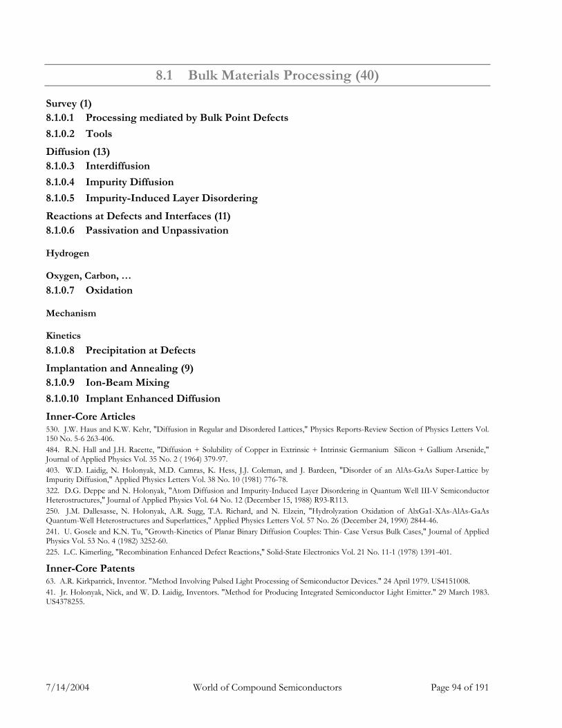
7/14/2004 World of Compound Semiconductors Page 94 of 191
8.1 Bulk Materials Processing (40)
Survey (1) 8.1.0.1 Processing mediated by Bulk Point Defects
8.1.0.2 Tools
Diffusion (13) 8.1.0.3 Interdiffusion
8.1.0.4 Impurity Diffusion
8.1.0.5 Impurity-Induced Layer Disordering
Reactions at Defects and Interfaces (11) 8.1.0.6 Passivation and Unpassivation
Hydrogen
Oxygen, Carbon, …
8.1.0.7 Oxidation
Mechanism
Kinetics
8.1.0.8 Precipitation at Defects
Implantation and Annealing (9) 8.1.0.9 Ion-Beam Mixing
8.1.0.10 Implant Enhanced Diffusion
Inner-Core Articles 530. J.W. Haus and K.W. Kehr, "Diffusion in Regular and Disordered Lattices," Physics Reports-Review Section of Physics Letters Vol. 150 No. 5-6 263-406. 484. R.N. Hall and J.H. Racette, "Diffusion + Solubility of Copper in Extrinsic + Intrinsic Germanium Silicon + Gallium Arsenide," Journal of Applied Physics Vol. 35 No. 2 ( 1964) 379-97. 403. W.D. Laidig, N. Holonyak, M.D. Camras, K. Hess, J.J. Coleman, and J. Bardeen, "Disorder of an AlAs-GaAs Super-Lattice by Impurity Diffusion," Applied Physics Letters Vol. 38 No. 10 (1981) 776-78. 322. D.G. Deppe and N. Holonyak, "Atom Diffusion and Impurity-Induced Layer Disordering in Quantum Well III-V Semiconductor Heterostructures," Journal of Applied Physics Vol. 64 No. 12 (December 15, 1988) R93-R113. 250. J.M. Dallesasse, N. Holonyak, A.R. Sugg, T.A. Richard, and N. Elzein, "Hydrolyzation Oxidation of AlxGa1-XAs-AlAs-GaAs Quantum-Well Heterostructures and Superlattices," Applied Physics Letters Vol. 57 No. 26 (December 24, 1990) 2844-46. 241. U. Gosele and K.N. Tu, "Growth-Kinetics of Planar Binary Diffusion Couples: Thin- Case Versus Bulk Cases," Journal of Applied Physics Vol. 53 No. 4 (1982) 3252-60. 225. L.C. Kimerling, "Recombination Enhanced Defect Reactions," Solid-State Electronics Vol. 21 No. 11-1 (1978) 1391-401.
Inner-Core Patents 63. A.R. Kirkpatrick, Inventor. "Method Involving Pulsed Light Processing of Semiconductor Devices." 24 April 1979. US4151008. 41. Jr. Holonyak, Nick, and W. D. Laidig, Inventors. "Method for Producing Integrated Semiconductor Light Emitter." 29 March 1983. US4378255.

7/14/2004 World of Compound Semiconductors Page 95 of 191
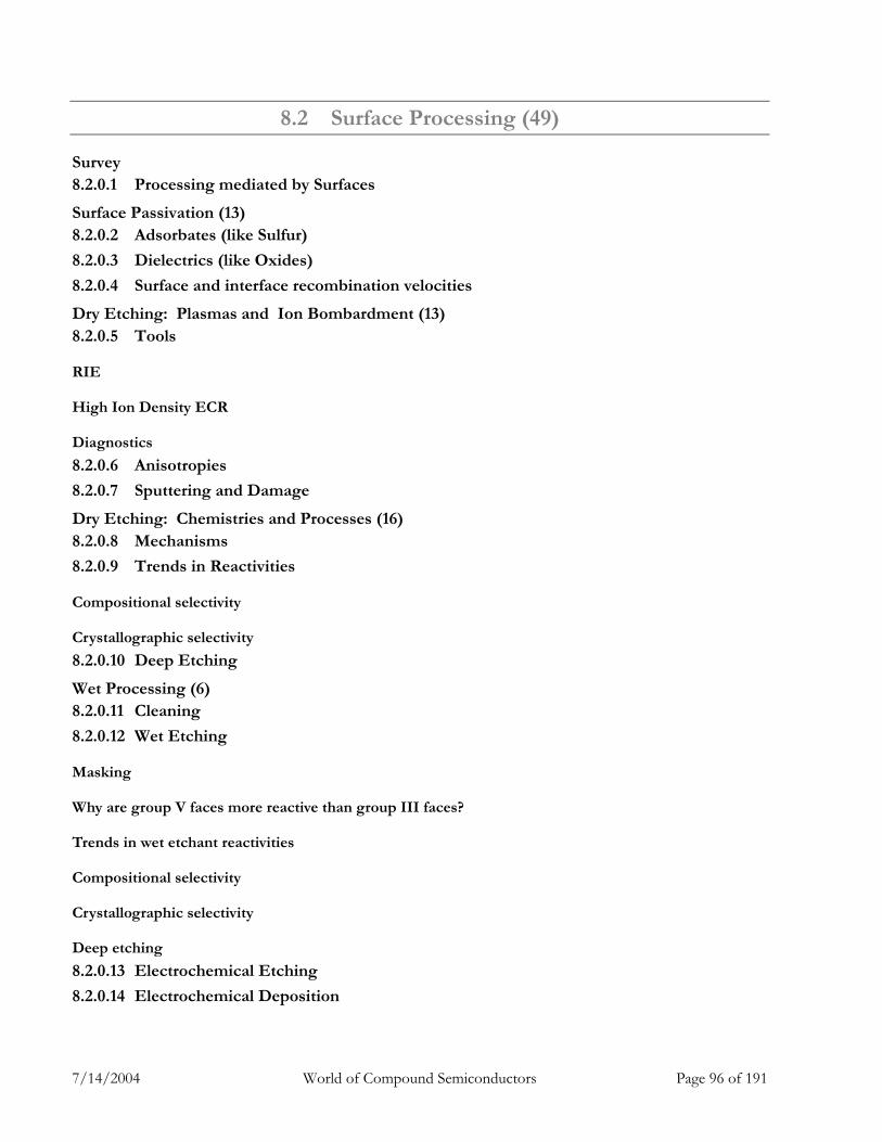
7/14/2004 World of Compound Semiconductors Page 96 of 191
8.2 Surface Processing (49)
Survey 8.2.0.1 Processing mediated by Surfaces
Surface Passivation (13) 8.2.0.2 Adsorbates (like Sulfur)
8.2.0.3 Dielectrics (like Oxides)
8.2.0.4 Surface and interface recombination velocities
Dry Etching: Plasmas and Ion Bombardment (13) 8.2.0.5 Tools
RIE
High Ion Density ECR
Diagnostics
8.2.0.6 Anisotropies
8.2.0.7 Sputtering and Damage
Dry Etching: Chemistries and Processes (16) 8.2.0.8 Mechanisms
8.2.0.9 Trends in Reactivities
Compositional selectivity
Crystallographic selectivity
8.2.0.10 Deep Etching
Wet Processing (6) 8.2.0.11 Cleaning
8.2.0.12 Wet Etching
Masking
Why are group V faces more reactive than group III faces?
Trends in wet etchant reactivities
Compositional selectivity
Crystallographic selectivity
Deep etching
8.2.0.13 Electrochemical Etching
8.2.0.14 Electrochemical Deposition
7/14/2004 World of Compound Semiconductors Page 97 of 191
Inner-Core Articles 260. E. Yablonovitch, C.J. Sandroff, R. Bhat, and T. Gmitter, "Nearly Ideal Electronic-Properties of Sulfide Coated GaAs-Surfaces," Applied Physics Letters Vol. 51 No. 6 (August 10, 1987) 439-41. 239. F.J. Grunthaner, P.J. Grunthaner, R.P. Vasquez, B.F. Lewis, and A. Madhukar, "Local Atomic and Electronic-Structure of Oxide-GaAs and Interfaces Using High-Resolution Xps," Journal of Vacuum Science & Technology Vol. 16 No. 5 1443-53. 219. K. Kohler, J.W. Coburn, D.E. Horne, E. Kay, and J.H. Keller, "Plasma Potentials of 13.56-Mhz Rf Argon Glow-Discharges in a Planar System," Journal of Applied Physics Vol. 57 No. 1 (January 1, 1985) 59-66. 205. G.S. Selwyn, J. Singh, and R.S. Bennett, "Insitu Laser Diagnostic Studies of Plasma-Generated Contamination," Journal of Vacuum Science & Technology a-Vacuum Films Vol. 7 No. 4 (1989) 2758-65. 201. C.C. Chang, P.H. Citrin, and B. Schwartz, "Chemical Preparation of GaAs Surfaces and Their Characterization by Auger-Electron and X-Ray Spectroscopies," Journal of Vacuum Science & Technology Vol. 14 No. 4 (1977) 943-52.
7/14/2004 World of Compound Semiconductors Page 98 of 191
8.3 Thin Films (32)
Survey (1)
Tools and Processes (8) 8.3.0.1 Sputtering
8.3.0.2 Evaporation
8.3.0.3 CVD
8.3.0.4 Diagnostics
8.3.0.5 Dielectrics, Metals
8.3.0.6 Trade-offs and Trends in Uniformity, Rate, Flexibility, Composition, Microstructure
Ohmic Contacts (14) 8.3.0.7 Alloyed and Unalloyed Contactds
8.3.0.8 p and n-yype Contacts
8.3.0.9 GaAs and InP
8.3.0.10 GaN
Shottky Contacts (9) 8.3.0.11 Formation Processes
8.3.0.12 Trends with Bandgap and Materials
8.3.0.13 Superconducting Contacts
Inner-Core Patents 51. M.F. Brady, I. J. K. Dorey, and Jr. A. L. Helms, Inventors. "Photolithographic Processes Using Thin
Coatings of Refractory Metal Silicon Nitrides As Antireflection Layers." At&T Bell Laboratories. 19 November 1991. US5066615.

7/14/2004 World of Compound Semiconductors Page 99 of 191
7/14/2004 World of Compound Semiconductors Page 100 of 191
8.4 Lithography and Substrate Engineering (31)
Survey
Lithography (6) 8.4.0.1 Photopolymerization and depolymerization
8.4.0.2 Photomasks
8.4.0.3 Contact and near-contact mask alignment
8.4.0.4 Projection lithography
8.4.0.5 Near-field holography
8.4.0.6 Direct atom manipulation
8.4.0.7 E-Beam Lithography
Bulk Substrates (2)
Substrate Engineering (7) 8.4.0.8 Cleaning
8.4.0.9 Cleaving
8.4.0.10 Bonding
8.4.0.11 Lift-Off
8.4.0.12 CMP
8.4.0.13 Compliant Substrates
8.4.0.14 HVPE
8.4.0.15 Plating
Inner-Core Articles 242. E. Yablonovitch, T. Gmitter, J.P. Harbison , and R. Bhat, "Extreme Selectivity in the Lift-Off of Epitaxial GaAs Films," Applied Physics Letters Vol. 51 No. 26 (December 28, 1987) 2222-24 .
Inner-Core Patents 90. M. Bruel, Inventor. "Process for the Production of Thin Semiconductor Material Films." 20 December 1994. US5374564. 87. T. Enomoto, M. Yasumoto, and H. Hayama, Inventors. "Process of Fabricating Three-Dimensional Semiconductor Device." 16 September 1986. US4612083. 59. T.J. Gmitter and E. Yablonovitch, Inventors. "Lift-Off and Subsequent Bonding of Epitaxial Films." Inc. Bell Communications Research. 28 November 1989. US4883561. 54. K.P. Stuby, Inventor. "Hourglass Shaped Conductive Connection Through Semiconductor Structures." 7 March 1972. US3648131. 50. T.J. Gmitter and E. Yablonovitch, Inventors. "Method for Lifting-Off Epitaxial Films." 11 July 1989. US4846931. 46. A. Reisman and W.-K. Chu, Inventors. "Method of Forming a Nonsilicon Semiconductor on Insulator Structure." 2 January 1990. US4891329.
7/14/2004 World of Compound Semiconductors Page 101 of 191
42. M. Bruel, Inventor. "Method for Placing Semiconductive Plates on a Support." 24 September 1996. US5559043. 42. B. Lischke, Inventor. "Lithographic Apparatus for the Production of Microstructures." 9 February 1988. US4724328. 41. M. Bruel, Inventor. "Process for the Production of a Relief Structure on a Semiconductor Material Support." 27 February 1996. US5494835.
7/14/2004 World of Compound Semiconductors Page 102 of 191
99 EELLEECCTTRROONNIICCSS ((7755)) Survey of Electronics (2)
Describes the technology and applications of devices which make use of bandgap nanoscience in compound semiconductor materials
These devices are categorized according to whether they are purely electronic, or optoelectronic (7-9) In Chapters 7-9 I describe how all of these materials, nanoscience and nanotechnology building blocks
result in powerful new electronic and photonic devices. I also describe the markets and economics associated with these devices – why they are useful today, and how they can improve to become more useful tomorrow.
Chapter 8 describes electronic devices Chapters 9 and 10 describe optoelectronic devices – first those in which light propagates “in the plane” of the
wafer, and second those in which light propagates “out of the plane” of the wafer Chapter 11 describes the applications and markets for these devices

7/14/2004 World of Compound Semiconductors Page 103 of 191
7/14/2004 World of Compound Semiconductors Page 104 of 191
9.1 MESFETs, MISFETs, HEMTs (41)
Survey
Basic geometry and equations (11) 9.1.0.1 Enhancement and Depletion Mode FETs
9.1.0.2 N-channel and P-channel FETs
9.1.0.3 MESFETs vs MISFETs
9.1.0.4 Ballistic transport
9.1.0.5 Vertical FETs
Fabrication (7) 9.1.0.6 Self-alignment
9.1.0.7 Ion implantation
9.1.0.8 Non-epi vs epi devices
9.1.0.9 Epi tolerances
Performance scaling (4) 9.1.0.10 Speed (small signal for analog, large signal for digital)
9.1.0.11 Power
9.1.0.12 Noise for digital
9.1.0.13 Linearity for analog
9.1.0.14 Integrability
7/14/2004 World of Compound Semiconductors Page 105 of 191
HEMTs (8)
Modulation doping
GaAs vs InP vs InAs vs InSb
Speed (small signal for analog, large signal for digital)
Power
Noise for digital
Linearity for analog
Integrability
Fabrication (5) 9.1.0.15 Delta doping
9.1.0.16 Insulating buffers
9.1.0.17 Selective etch stops
9.1.0.18 Self-alignment
9.1.0.19 Epi tolerances
Magnetoresistors (1) 9.1.0.20 Hall effect devices
Nanodevices 9.1.0.21 Ballistic Devices
9.1.0.22 Single-Electron Devices
9.1.0.23 Quantum Interference Devices
Inner-Core Articles 420. T. Mimura, S. Hiyamizu, T. Fujii, and K. Nanbu, "A New Field-Effect Transistor With Selectively Doped GaAs-N-AlxGa1-XAs Heterojunctions," Japanese Journal of Applied Physics Vol. 19 No. 5 (1980) L225-L227.
7/14/2004 World of Compound Semiconductors Page 106 of 191
9.2 Diodes, Triodes, Mixers, HBTs (35)
Survey
Diodes, Triodes, Mixers (4) 9.2.0.1 Radiometric detectors
9.2.0.2 Gunn effect and Gunn diodes
Oscillatory phenomena in which moving domains of higher electric field and charge density:
nucleate (usually at the cathode),
drift at the peak electron saturation velocity across a sample,
are sharpened and stabilized as they drift by negative differential resistance which causes electron bunching,
then annihilate at the anode
Typical saturation velocities are 1e7cm/s and typical sample lengths are 10microns, so typical oscillation frequencies are 10GHz, in the microwave range
The key is negative differential resistance, which can occur in bulk materials (the effect was first observed in n-GaAs and in tunneling (Esaki) and resonant tunneling diodes
HBTs: Basic Geometry and Performance Scaling (7) 9.2.0.3 Homojunction vs heterojunction devices
9.2.0.4 GaAs vs InP vs GaN
9.2.0.5 Surface recombination
9.2.0.6 Speed (small signal for analog, large signal for digital)
9.2.0.7 Power
9.2.0.8 Noise for digital
9.2.0.9 Linearity for analog
9.2.0.10 Integrability
HBTs: Advanced Fabrication (4) 9.2.0.11 HBTs: Fabrication
9.2.0.12 Graded layers
9.2.0.13 Heavily doped bases
9.2.0.14 Surface passivated structures
Nanodevices and Antennas 9.2.0.15 Tunneling
9.2.0.16 Resonant Tunneling
9.2.0.17 Field emitters and vacuum electronics
7/14/2004 World of Compound Semiconductors Page 107 of 191
9.2.0.18 Antennas
Inner-Core Articles 606. T.C.L. Sollner, W.D. Goodhue, P.E. Tannenwald, C.D. Parker, and D.D. Peck, "Resonant Tunneling Through Quantum Wells at Frequencies Up to 2.5 Thz," Applied Physics Letters Vol. 43 No. 6 (1983) 588-90. 539. H. Kroemer, "Heterostructure Bipolar-Transistors and Integrated-Cirucuts," Proceedings of the IEEE Vol. 70 No. 1 (1982) 13-25. 491. C.J. Sandroff, R.N. Nottenburg, J.C. Bischoff, and R. Bhat, "Dramatic Enhancement in the Gain of a GaAs/AlGaAs Heterostructure Bipolar-Transistor by Surface Chemical Passivation," Applied Physics Letters Vol. 51 No. 1 (July 6, 1987) 33-35. 413. J.B. Gunn, "Microwave Oscillations of Current in III-V Semiconductors," Solid State Communications Vol. 1 No. 4 (1963) 88-91. 327. S. Luryi, "Frequency Limit of Double-Barrier Resonant-Tunneling Oscillators," Applied Physics Letters Vol. 47 No. 5 (September 1, 1985) 490-492. 223. E.R. Brown, J.R. Soderstrom, C.D. Parker, L.J. Mahoney, Molvar, and T.C. Mcgill, "Oscillations Up to 712 Ghz in InAs/Alsb Resonant-Tunneling Diodes," Applied Physics Letters Vol. 58 No. 20 (May 20, 1991) 2291-93. 210. H.G. Roskos, M.C. Nuss, J. Shah, K. Leo, D.A.B. Miller, A.M. Fox, S. Schmittrink, and K. Kohler, "Coherent Submillimeter-Wave Emission From Charge Oscillations in a Double-Well Potential," Physical Review Letters Vol. 68 No. 14 (April 6, 1992) 2216-19.
Inner-Core Patents 43. R.F. Greene and H. F. Gray, Inventors. "Field Emitter Array." The United States of America as Represented by the Secretary of the Navy. 22 September 1992. US5150192.
7/14/2004 World of Compound Semiconductors Page 108 of 191
1100 IINN--PPLLAANNEE OOPPTTOOEELLEECCTTRROONNIICCSS ((116688)) Survey of In-Plane Optoelectronics (0) Mostly edge-emitting lasers

7/14/2004 World of Compound Semiconductors Page 109 of 191
7/14/2004 World of Compound Semiconductors Page 110 of 191
10.1 Broad Stripe Double Heterostructure Lasers (30)
Survey
Basic Geometry, Equations and Performance (10) 10.1.0.1 Spontaneous and stimulated emission
10.1.0.2 Gain and loss
10.1.0.3 Transparency
10.1.0.4 Below threshold and above threshold characteristics
10.1.0.5 Confinement factor
10.1.0.6 Vertical Optical Cavity Engineering
Separate Confinement GRINSCH structures
10.1.0.7 Doped vs undoped active regions
10.1.0.8 Temperature dependence of gain and wavelength
Materials Engineering (20) 10.1.0.9 GaAs-based (AlInGaAs, InAlGaP, InGaAsN)
10.1.0.10 InP-based (InGaAsP, InAlGaAs)
10.1.0.11 GaN-based
10.1.0.12 Aging
10.1.0.13 Limits to Performance
Reliability -- Facet Damage Heat dissipation – cw vs pulsed operation
10.1.0.14 Strain
Inner-Core Articles 310. R.N. Hall, R.O. Carlson, T.J. Soltys, G.E. Fenner, and J.D. Kingsley, "Coherent Light Emission From Gaas Junctions," Physical Review Letters Vol. 9 No. 9 ( 1962) 366-69. 297. E. Yablonovitch and E.O. Kane, "Reduction of Lasing Threshold Current-Density by the Lowering of Valence Band Effective Mass," Journal of Lightwave Technology Vol. 4 No. 5 (May, 1986) 504-6. 270. M.I. Nathan, W.P. Dumke, G. Burns, F.H. Dill, and G. Lasher, "Stimulated Emission of Radiation From Gaas P-n Junctions," Applied Physics Letters Vol. 1 No. 3 ( 1962) 62-64. 204. W.T. Tsang, "Extremely Low Threshold (Alga)As Graded-Index Waveguide Separate Confinement Heterostructure Lasers Grown by Molecular-Beam Epitaxy," Applied Physics Letters Vol. 40 No. 3 (1982) 217-19. 202. M. Asada and Y. Suematsu, "Density-Matrix Theory of Semiconductor-Lasers With Broadening Model: Gain and Gain-Suppression in Semiconductor-Lasers," IEEE Journal of Quantum Electronics Vol. 21 No. 5 (1985) 434-42.
Inner-Core Patents 70. N. Okazaki and others, Inventors. "Gallium Nitride Group Compound Semiconductor Laser Diode." 21 September 1993. US5247533.
7/14/2004 World of Compound Semiconductors Page 111 of 191
7/14/2004 World of Compound Semiconductors Page 112 of 191
10.2 Gain and Bandwidth Engineering (32)
Survey
Quantum Wells (18) 10.2.0.1 Optimal number of wells
10.2.0.2 Many-body effects
10.2.0.3 Semi-empirical gain vs n vs j equations
10.2.0.4 Carrier confinement issues
10.2.0.5 High temperature operation
10.2.0.6 High injection operation
Quantum Wires (6)
Quantum Dots (6) 10.2.0.7 Carrier confinement issues
10.2.0.8 High temperature operation
Quantum Cascade Lasers (2)
Transient Response of Lasers and Amplifiers (11) 10.2.0.9 Gain
10.2.0.10 Electrons and Holes (Recombination)
10.2.0.11 Electrons and Holes (Transport)
10.2.0.12 Photons
10.2.0.13 Index Changes and Chirping
Inner-Core Articles 895. S. Nakamura, M. Senoh, S. Nagahama, N. Iwasa, T. Yamada, T. Matsushita, H. Kiyoku, and Y. Sugimoto, "InGaN-Based Multi-Quantum-Well-Structure Laser Diodes," Japanese Journal of Applied Physics Part 2-Letters Vol. 35 No. 1B (January 15, 1996) L74-L76. 891. Y. Arakawa and H. Sakaki, "Multidimensional Quantum Well Laser and Temperature- of Its Threshold Current," Applied Physics Letters Vol. 40 No. 11 (1982) 939-41. 593. J. Faist, F. Capasso, D.L. Sivco, C. Sirtori, A.L. Hutchinson, and A.Y. Cho, "Quantum Cascade Laser," Science Vol. 264 No. 5158 (April 22, 1994) 553-56. 397. N. Holonyak, R.M. Kolbas, R.D. Dupuis, and P.D. Dapkus, "Quantum-Well Heterostructure Lasers," IEEE Journal of Quantum Electronics Vol. 16 No. 2 (1980) 170-186. 358. A.R. Adams, "Band-Structure Engineering for Low-Threshold High-Efficiency Semiconductor-Lasers," Electronics Letters Vol. 22 No. 5 (1986) 249-50. 294. M. Asada, Y. Miyamoto, and Y. Suematsu, "Gain and the Threshold of 3-Dimensional Quantum-Box Lasers," IEEE Journal of Quantum Electronics Vol. 22 No. 9 (1986) 1915-21. 285. Y. Arakawa and A. Yariv, "Quantum-Well Lasers Gain, Spectra, Dynamics," IEEE Journal of Quantum Electronics Vol. 22 No. 9 (1986) 1887-99. 285. N. Kirstaedter, N.N. Ledentsov, M. Grundmann, D. Bimberg, S.S. Ruvimov, M.V. Maximov, P.S. Kopev, Z.I. Alferov, U. Richter, P. Werner, U. Gosele, and J. Heydenreich, "Low-Threshold, Large T-O Injection-Laser Emission From (Inga)As Quantum Dots," Electronics Letters Vol. 30 No. 17 (August 18, 1994) 1416-17. 273. Y. Narukawa, Y. Kawakami, M. Funato, S. Fujita, S. Fujita, and S. Nakamura, "Role of Self-Formed InGaN Quantum Dots for Exciton Localization in the Purple Laser Diode Emitting at 420 Nm," Applied Physics Letters Vol. 70 No. 8 (February 24, 1997) 981-83. 227. W.T. Tsang, "Extremely Low Threshold (AlGa)As Modified Multiquantum Well Heterostructure Lasers Grown by Molecular-Beam Epitaxy," Applied Physics Letters Vol. 39 No. 10 (1981) 786-88.
7/14/2004 World of Compound Semiconductors Page 113 of 191
7/14/2004 World of Compound Semiconductors Page 114 of 191
10.3 Transverse Mode and Polarization Engineering (18)
Survey
Lateral Guiding Mechanisms (5) 10.3.0.1 Gain Guiding
10.3.0.2 Index Guiding
10.3.0.3 Antiguiding
10.3.0.4 Photocarrier and thermal lensing
10.3.0.5 Diffraction
Geometries and Fabrication (10) 10.3.0.6 Buried Heterostructures
10.3.0.7 Channeled substrate
10.3.0.8 Stripe
10.3.0.9 Buried oxide
Laterally Coupled Arrays (3) 10.3.0.10 Symmetric supermodes
10.3.0.11 Antisymmetric supermodes
Inner-Core Articles 222. K. Aiki, M. Nakamura, T. Kuroda, J. Umeda, R. Ito, N. Chinone, and M. Maeda, "Transverse Mode
Stabilized Alx Ga1-XAs Injection-Lasers Channeled-Substrate-Planar Structure," IEEE Journal of Quantum Electronics Vol. 14 No. 2 (1978) 89-94.

7/14/2004 World of Compound Semiconductors Page 115 of 191
7/14/2004 World of Compound Semiconductors Page 116 of 191
10.4 Longitudinal Mode and Noise Engineering (34)
Survey
Cavity Engineering (6) 10.4.0.1 Short cavities
10.4.0.2 Composite cavities
10.4.0.3 Temperature issues
Distributed Feedback (10) 10.4.0.4 Distributed feedback (DFBs, DBRs)
10.4.0.5 Coupled modes
10.4.0.6 Homogenous and inhomogeneous gain
Noise, Stability, Linewidths (18) 10.4.0.7 AM and FM noise
10.4.0.8 Phase locking
10.4.0.9 Squeezed States; Chaos
10.4.0.10 Intermodulation and harmonic distortion
10.4.0.11 External optical feedback
Inner-Core Articles 795. C.H. Henry, "Theory of the Linewidth of Semiconductor-Lasers," IEEE Journal of Quantum Electronics Vol. 18 No. 2 (1982) 259-64. 261. Y. Yamamoto, S. Machida, and O. Nilsson, "Amplitude Squeezing in a Pump-Noise-Suppressed Laser Oscillator," Physical Review A Vol. 34 No. 5 (1986) 4025-42. 249. S. Machida, Y. Yamamoto, and Y. Itaya, "Observation of Amplitude Squeezing in a Constant-Current Semiconductor-Laser," Physical Review Letters Vol. 58 No. 10 (March 9, 1987) 1000-1003. 214. C.H. Henry, "Theory of Spontaneous Emission Noise in Open Resonators Application to Lasers and Optical Amplifiers," Journal of Lightwave Technology Vol. 4 No. 3 (1986) 288-97. 207. R.W. Tkach and A.R. Chraplyvy, "Regimes of Feedback Effects in 1.5-Mu-M Distributed Feedback Lasers," Journal of Lightwave Technology Vol. 4 No. 11 (1986) 1655-61. 200. B. Dahmani, L. Hollberg, and R. Drullinger, "Frequency Stabilization of Semiconductor-Lasers by Resonant Optical Feedback," Optics Letters Vol. 12 No. 11 (1987) 876-78.

7/14/2004 World of Compound Semiconductors Page 117 of 191
7/14/2004 World of Compound Semiconductors Page 118 of 191
10.5 Hybrid and Integrated Devices (26)
Survey
Externally Modulated Lasers (12) 10.5.0.1 Gain Modulation
10.5.0.2 Acousto-optic
10.5.0.3 Electroabsorptive
10.5.0.4 Frequency Modulation
10.5.0.5 Self-Phase-Modulation and Mode Locking
Optical Modulators (3)
Microcavity Lasers (2)
Lasers and Nonlinear Optical Elements (4) 10.5.0.6 Intracavity frequency converters
10.5.0.7 Lasers controlling other lasers
Incoherently Coupled Photonic Integration (13) 10.5.0.8 EAM lasers
10.5.0.9 Monitor photodiodes
10.5.0.10 Acoustooptic modulators
10.5.0.11 Microdisk lasers, resonators and filters
10.5.0.12 Spot-size converters
10.5.0.13 Uncoupled laser arrays
Coherently Coupled Photonic Integration (9) 10.5.0.14 Waveguides and bends
10.5.0.15 Filters and waveguide-coupling modulators
10.5.0.16 Switches
Inner-Core Articles 305. T.H. Wood, C.A. Burrus, D.A.B. Miller, D.S. Chemla, T.C. Damen, and W. Wiegmann, "High-Speed
Optical Modulation With GaAs/GaAlAs Quantum Wells in a P-I-N-Diode Structure," Applied Physics Letters Vol. 44 No. 1 (1984) 16-18. 303. M.M. Fejer, G.A. Magel, D.H. Jundt, and R.L. Byer, "Quasi-Phase-Matched 2nd Harmonic-Generation: Tuning and Tolerances," IEEE Journal of Quantum Electronics Vol. 28 No. 11 2631-54.
266. S. Kobayashi, Y. Yamamoto, M. Ito, and T. Kimura, "Direct Frequency-Modulation in AlGaAs Semiconductor-," IEEE Journal of Quantum Electronics Vol. 18 No. 4 (1982) 582-95.
Inner-Core Patents 57. D.R. Scifres and others, Inventors. "Frequency Converted Laser Diode and Lens System Therefor." 14 June 1994. US5321718. 53. H. Terui and others, Inventors. "Hybrid Optical Integrated Circuit." 14 June 1988. US4750799. 46. G.F. Williams, Inventor. "Wavelength Division Multiplexing Optical Communications Systems." At&T Bell Laboratories. 27 May 1986. US4592043.
7/14/2004 World of Compound Semiconductors Page 119 of 191
41. D.R. Scifres, D. F. Welch, and D. G. Mehuys , Inventors. "Semiconductor Laser With Integral Spatial Mode Filter." 21 February 1995. US5392308. 41. D.F. Welch and R. G. Waarts, Inventors. "Coupling Arrangements for Frequency-Doubled Diode Lasers." Inc. Spectra Diode Laboratories. 9 February 1993. US5185752.
7/14/2004 World of Compound Semiconductors Page 120 of 191
1111 OOUUTT--OOFF--PPLLAANNEE OOPPTTOOEELLEECCTTRROONNIICCSS
((6699,,4477))

7/14/2004 World of Compound Semiconductors Page 121 of 191
7/14/2004 World of Compound Semiconductors Page 122 of 191
11.1 Survey of Out-of-Plane Optoelectronics (0)

7/14/2004 World of Compound Semiconductors Page 123 of 191
7/14/2004 World of Compound Semiconductors Page 124 of 191
11.2 LEDs (18)
Survey
AlGaAs and AlGaInP IR and Red (3)
AlGaInN Green, Blue and UV (12)
Light Extraction Engineering (3) 11.2.0.1 Light cones
11.2.0.2 Texturing
11.2.0.3 Transparent substrates
11.2.0.4 Transparent electrodes
11.2.0.5 Wafer bonding
11.2.0.6 Resonant-cavity LEDs
11.2.0.7 Superluminescent LEDs
Inner-Core Articles 811. S. Nakamura, T. Mukai, and M. Senoh, "Candela-Class High-Brightness InGaN/AlGaN Double-Heterostructure Blue-Light-Emitting Diodes," Applied Physics Letters Vol. 64 No. 13 (March 28, 1994) 1687-89. 389. S. Nakamura, N. Senoh, N. Iwasa, and S. Nagahama, "High-Brightness InGaN Blue, Green and Yellow Light-Emitting-Diodes With Quantum-Well Structures," Japanese Journal of Applied Physics Part 2-Letters Vol. 34 No. 7A (July 1, 1995) L797-L799. 301. S. Nakamura, M. Senoh, N. Iwasa, S. Nagahama, T. Yamada, and T. Mukai, "Superbright Green InGaN Single-Quantum-Well-Structure Light-Emitting-Diodes," Japanese Journal of Applied Physics Part 2-Letters Vol. 34 No. 10B (October 15, 1995) L1332-L1335. 261. S. Nakamura, T. Mukai, and M. Senoh, "High-Power GaN P-N-Junction Blue-Light-Emitting Diodes," Japanese Journal of Applied Physics Part 2-Letters Vol. 30 No. 12A (December 1, 1991) L1998-L2001.
Inner-Core Patents 52. S. Nakamura, T. Mukai, and N. Iwasa, Inventors. "Light-Emitting Gallium Nitride-Based Compound Semiconductor Device." Ltd. Nichia Chemical Industries. 26 November 1996. US5578839. 48. N. Iwasa, S. Nakamura, and T. Mukai, Inventors. "Light-Emitting Gallium Nitride-Based Compound Semiconductor Device." 26 November 1996. US5578839.

7/14/2004 World of Compound Semiconductors Page 125 of 191
7/14/2004 World of Compound Semiconductors Page 126 of 191
11.3 VCSELs (28)
Survey
Gain and Feedback Engineering (15) 11.3.0.1 Equations
11.3.0.2 Cavity length
11.3.0.3 DBRs
11.3.0.4 Active regions
Transverse Mode Engineering (9) 11.3.0.5 Gain Guiding
11.3.0.6 Selective oxidation
11.3.0.7 Transverse mode control
11.3.0.8 Polarization
11.3.0.9 Arrays
Carrier Engineering and Speed (4) 11.3.0.10 Current spreading and crowding
11.3.0.11 Speed
11.3.0.12 Reliability
11.3.0.13 Noise
InP and GaN based VCSELs
Inner-Core Patents 63. Jr. Schneider and others, Inventors. "Efficient Semiconductor Light-Emitting Device and Method." 20
February 1996. US5493577. 54. J.L. Jewell and A. Scherer, Inventors. "Surface Emitting Semiconductor Laser." 14 August 1990.
US4949350. 41. Y.H. Lee and B. Tell, Inventors. "Top-Emitting Surface Emitting Laser Structures." 19 May 1992.
US5115442.

7/14/2004 World of Compound Semiconductors Page 127 of 191
7/14/2004 World of Compound Semiconductors Page 128 of 191
11.4 Detectors and Solar Cells (25)
Survey
PIN Photodiodes (2) 11.4.0.1 Figures of merit – Detectivity, Noise-equivalent power, Speed
11.4.0.2 PIN Photodiodes
11.4.0.3 Photovoltaic IR detectors
11.4.0.4 Fabrication
Avalanche Photodiodes (10)
QWIPs (9)
Imaging Detectors (2) 11.4.0.5 Schottky diodes
11.4.0.6 CCDs
Laterally Collected Photodetectors (2)
Single Junction Solar Cells (5) 11.4.0.7 Figures of merit – Efficiency, Cost
11.4.0.8 Fabrication
Multijunction Solar Cells (5)
Light Input Engineering (1) 11.4.0.9 Internal and external efficiencies
11.4.0.10 Texturing
Photoelectrochemical Solar Cells (5)
Inner-Core Patents 53. R.J. McIntyre and P. P. Webb, Inventors. "Avalanche Photodiode Array." Rca Inc. 3 July 1984. US4458260. 46. S. Yamazaki, Inventor. "Semiconductor Photoelectric Conversion Device." 16 December 1980. US4239554. 45. M.K. Goldstein, Inventor. "Multiband Emitter Matched to Multilayer Photovoltaic Collector." 11 October 1988. US4776895.

7/14/2004 World of Compound Semiconductors Page 129 of 191
7/14/2004 World of Compound Semiconductors Page 130 of 191
11.5 Modulators, Gates and Hybrid Devices (24)
Survey
Light Valves and Modulators (7) 11.5.0.1 Schottky diodes
11.5.0.2 Saturable absorbers
11.5.0.3 Photobleaching and holographic memories
Bistable Devices (14) 11.5.0.4 Excitons and Etalons
11.5.0.5 SEEDs
Hybrid Devices (3)
Inner-Core Patents 57. D.A.B. Miller, Inventor. "Nonlinear and Bistable Optical Device." At&T Bell Laboratories. 8 October
1985. US4546244. 48. M.A. Reed, G. A. Frazier, and W. R. Frensley, Inventors. "Spatial Light Modulator." 10 November 1987.
US4705361. 42. D.A.B. Miller, Inventor. "Nonlinear and Bistable Optical Device." 29 December 1987. US4716449.

7/14/2004 World of Compound Semiconductors Page 131 of 191
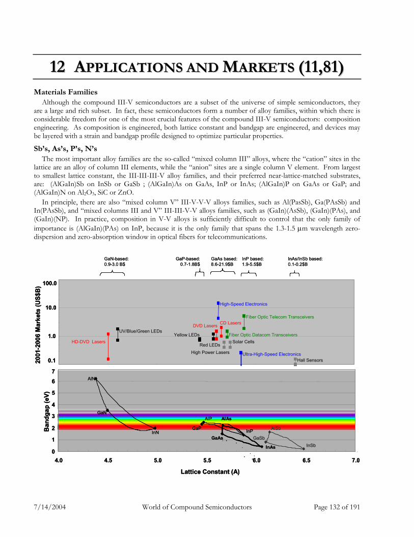
7/14/2004 World of Compound Semiconductors Page 132 of 191
1122 AAPPPPLLIICCAATTIIOONNSS AANNDD MMAARRKKEETTSS ((1111,,8811)) Materials Families
Although the compound III-V semiconductors are a subset of the universe of simple semiconductors, they are a large and rich subset. In fact, these semiconductors form a number of alloy families, within which there is considerable freedom for one of the most crucial features of the compound III-V semiconductors: composition engineering. As composition is engineered, both lattice constant and bandgap are engineered, and devices may be layered with a strain and bandgap profile designed to optimize particular properties.
Sb’s, As’s, P’s, N’s The most important alloy families are the so-called “mixed column III” alloys, where the “cation” sites in the
lattice are an alloy of column III elements, while the “anion” sites are a single column V element. From largest to smallest lattice constant, the III-III-III-V alloy families, and their preferred near-lattice-matched substrates, are: (AlGaIn)Sb on InSb or GaSb ; (AlGaIn)As on GaAs, InP or InAs; (AlGaIn)P on GaAs or GaP; and (AlGaIn)N on Al2O3, SiC or ZnO.
In principle, there are also “mixed column V” III-V-V-V alloys families, such as Al(PasSb), Ga(PAsSb) and In(PAsSb), and “mixed columns III and V” III-III-V-V alloys families, such as (GaIn)(AsSb), (GaIn)(PAs), and (GaIn)(NP). In practice, composition in V-V alloys is sufficiently difficult to control that the only family of importance is (AlGaIn)(PAs) on InP, because it is the only family that spans the 1.3-1.5 µm wavelength zero-dispersion and zero-absorption window in optical fibers for telecommunications.
GaN-based: 0.9-3.0 B$
GaP-based: 0.7-1.8B$
GaAs based: 8.6-21.9$B
InP based: 1.9-5.5$B
InAs/InSb based: 0.1-0.2$B
0
1
2
3
4
5
6
7
4.0 4.5 5.0 5.5 6.0 6.5 7.0
Lattice Constant (A)
Ban
dgap
(eV)
AlN
GaN
InNGaP
AlP
InP
AlAs
GaAs
InAs
GaSb
AlSb
InSb
0.1
1.0
10.0
100.0
2001
-200
6 M
arke
ts (U
S$B
)
HD-DVD Lasers
UV/Blue/Green LEDs
Hall SensorsUltra-High-Speed Electronics
Fiber Optic Telecom Transceivers
High-Speed Electronics
Yellow LEDs
Red LEDs
DVD Lasers
Fiber Optic Datacom Transceivers Solar Cells
CD Lasers
High Power Lasers
GaN-based: 0.9-3.0 B$
GaP-based: 0.7-1.8B$
GaAs based: 8.6-21.9$B
InP based: 1.9-5.5$B
InAs/InSb based: 0.1-0.2$B
0
1
2
3
4
5
6
7
4.0 4.5 5.0 5.5 6.0 6.5 7.0
Lattice Constant (A)
Ban
dgap
(eV)
AlN
GaN
InNGaP
AlP
InP
AlAs
GaAs
InAs
GaSb
AlSb
InSb0
1
2
3
4
5
6
7
4.0 4.5 5.0 5.5 6.0 6.5 7.0
Lattice Constant (A)
Ban
dgap
(eV)
AlN
GaN
InNGaP
AlP
InP
AlAs
GaAs
InAs
GaSb
AlSb
InSb
0.1
1.0
10.0
100.0
2001
-200
6 M
arke
ts (U
S$B
)
HD-DVD Lasers
UV/Blue/Green LEDs
Hall SensorsUltra-High-Speed Electronics
Fiber Optic Telecom Transceivers
High-Speed Electronics
Yellow LEDs
Red LEDs
DVD Lasers
Fiber Optic Datacom Transceivers Solar Cells
CD Lasers
High Power Lasers
0.1
1.0
10.0
100.0
2001
-200
6 M
arke
ts (U
S$B
)
HD-DVD Lasers
UV/Blue/Green LEDs
Hall SensorsUltra-High-Speed Electronics
Fiber Optic Telecom Transceivers
High-Speed Electronics
Yellow LEDs
Red LEDs
DVD Lasers
Fiber Optic Datacom Transceivers Solar Cells
CD Lasers
High Power Lasers
7/14/2004 World of Compound Semiconductors Page 133 of 191
Chip Application Families Each of the III-V alloy families has a number of chip application families, determined by their unique ranges
of bandgaps and other properties. These applications are represented by the bars in the Facing Figure. The horizontal position of the bars corresponds to the substrates and materials family in the bottom Figure that the chips are fabricated from. The bottom of each bar represents the 2001 market size for those chips; the top of each bar represents the projected 2006 market size; and since the plot is a log plot, the length of the bars indicates the percentage market size growth rates.
Top 4 Chip Applications There are 4 “big” applications for compound III-V semiconductor chips. The first is high-speed electronics: the analog integrated circuits used as preamplifiers and power amplifiers
for wireless RF and microwave communications, and the high-speed digital integrated circuits used to drive fiber-optic transceivers. These electronic chips are based mostly on GaAs substrates and the AlGaInAs materials family.
The second is fiber-optics: the discrete or integrated lasers, modulators, amplifiers, switches and detectors used for sending and receiving optical signals through optical fibers. These optical chips are based mostly on InP substrates and the (AlGaIn)(PAs) materials family.
The third is optical storage: the (AlGaIn)As-based infrared lasers used for CDs, the GaAs and AlGaInP-based red lasers used for DVDs, and the GaN-based purple lasers that will soon be used for high-definition DVDs.
The fourth is solid-state lighting: the (AlGaIn)P-based red LEDs, and the GaN-based green, blue and UV LEDs that are used for power signaling and someday for general white lighting.
All Chip Applications All together, the 2001 compound III-V semiconductor chip market was roughly 12 US$B, and the 2006
projected market is roughly 32 US$B, a compound annual growth rate of roughly 20%. Indeed, this chip market is now approaching 10% of the 2001 Si chip market of roughly 150 US$B.
Inner-Core Articles 1060. S. Strife and H. Morkoc, "GaN, AlN, and InN - a Review," Journal of Vacuum Science & Technology B Vol. 10 No. 4 (July, 1992-August 31, 1992 ) 1237-66. 912. H. Morkoc, S. Strite, G.B. Gao, M.E. Lin, B. Sverdlov, and M. Burns, "Large-Band-Gap SiC, III-V Nitride, and II-VI ZnSe-Based Semiconductor-Device Technologies," Journal of Applied Physics Vol. 76 No. 3 (August 1, 1994) 1363-98. 248. S.N. Mohammad, A. Salvador, and H. Morkoc, "Emerging Gallium Nitride Based Devices," Proceedings of the IEEE Vol. 83 No. 10 (October, 1995) 1306-55. 233. R.F. Davis, "III-V Nitrides for Electronic and Optoelectronic Applications," Proceedings of the Ieee Vol. 79 No. 5 (1991) 702-12.

7/14/2004 World of Compound Semiconductors Page 134 of 191
12.1 Wireless Communications (7)
Survey
GaAs vs InP vs SiGe
RF Receivers (1) 12.1.0.1 Preamplifiers
RF Transmitters (4) 12.1.0.2 RF Output Amplifiers
12.1.0.3 Dual Mode (Analog and Digital)
Microwave Systems and Radars (2) 12.1.0.4 Si and ceramic packaging
Inner-Core Patents 53. R.C. Dixon and J. S. Vanderpool, Inventors. "Dual Mode Transmitter and Receiver." 1 March 1994. US5291516. 43. H. Mattila, J. Matero, and H. Pakonen, Inventors. "Dual Mode Amplifier With Bias Control." 11 July 1995. US5432473. 41. G.M. Cristiano, D. G. Schwent, and R. M. Osmani, Inventors. "Dual Mode Power Amplifier for Radiotelephone." 22 October 1991. US5060294.
7/14/2004 World of Compound Semiconductors Page 135 of 191
7/14/2004 World of Compound Semiconductors Page 136 of 191
12.2 Optical Communications (20)
Survey 12.2.0.1 Bandwidth – Distance Chart
WAN – Long-Haul
MAN – Metro
LAN – Campus
12.2.0.2 Dispersion – Wavelength – Linewidth Chart
12.2.0.3 Transverse vs Longitudinal Mode Chart
12.2.0.4 System noise, etc considerations on laser power, detector sensitivity, fiber or free-space loss, etc
12.2.0.5 Wavelength considerations
12.2.0.6 Materials considerations
Optical Couplers (12) 12.2.0.7 Multimode and Singlemode fibers
12.2.0.8 Coupling to fiber and spot size converters
12.2.0.9 Active alignment to fibers
Silicon Optical Benches (6)
Stabilized Light Sources (9) 12.2.0.10 Temperature stabilization
12.2.0.11 Amplitude stabilization
12.2.0.12 FP vs DFBs vs VCSELs
12.2.0.13 Wavelength stabilization
12.2.0.14 Reliability
Fiber Communications Systems (4) 12.2.0.15 WDM Transmitters
12.2.0.16 Fiber Amplifiers
EDFAs
Raman Amplifiers
12.2.0.17 Switches, Amplifiers, Receivers
SOAs
12.2.0.18 Drive Electronics
GaAs vs SiGe vs InP
7/14/2004 World of Compound Semiconductors Page 137 of 191
Free-Space Communications Systems
Inner-Core Patents 52. E.I. Gordon, R. J. Nielsen, and J. W. Stafford, Inventors. "Optoelectronics Package for a Semiconductor
Laser." 21 June 1988. US4752109. 51. W.H. Dufft, Inventor. "Encapsulated Light Source With Coupled Fiberguide." 27 October 1981.
US4296998. 50. H. Sato and others, Inventors. "Semiconductor Laser Apparatus." 6 July 1982. US4338577. 49. G.E. Blonder, Inventor. "Subassemblies for Optoelectronic Hybrid Integrated Circuits." 27 February
1990. US4904036. 46. T.A. Cook and M. C. Hudson, Inventors. "Light Source for Optical Waveguide Bundle." 13 April 1976.
US3950075. 44. J.S. Clanton, Inventor. "Electro Optical Transmission Line." 7 May 1974. US3809908. 44. D.R. Scifres, R. D. Burnham, and W. Streifer, Inventors. "Fiber Optic Laser Device and Light Emitter
Utilizing the Device." 9 November 1982. US4358851. 43. J. Kleefeld, J. Berger, and D. Mick, Inventors. "Temperature Stable Solid-State Laser Package." 19 January
1993. US5181214. 42. F.P. Kapron and D. B. Keck, Inventors. "Optical Waveguide Light Source Coupler." 18 December 1973.
US3779628. 41. T. Shibagaki and O. Kinoshita, Inventors. "Apparatus for Stabilizing the Optical Output Power of a
Semiconductor Laser." 22 March 1988. US4733398.
7/14/2004 World of Compound Semiconductors Page 138 of 191
12.3 Energy Conversion, Imaging, Sensing (10)
Survey
Position Sensing and Scanning (3) 12.3.0.1 Survey
12.3.0.2 Bar Code Scanners
12.3.0.3 CD Players and Writers
12.3.0.4 DVD Players and Writers
12.3.0.5 UDVD
Energy Conversion (2) 12.3.0.6 Survey
12.3.0.7 Terrestrial PV
Efficiency – Cost Considerations
12.3.0.8 Space PV
Weight -- Efficiency – Cost Considerations
Spectroscopy (2)
Imaging (3)
Inner-Core Patents 81. D.A. Christensen, Inventor. "Semiconductor Temperature Sensor." 30 January 1979. US4136566. 51. J.J. Hanak, Inventor. "Laser Processing Technique for Fabricating Series-Connected and Tandem Junction Series-Connected Solar Cells into a Solar Battery." 29 September 1981. US4292092. 50. D.B. Kay, Inventor. "Optical Scanning System With Wavelength Shift Correction." 31 January 1984. US4428643. 41. D.D. Buss, R. T. Bate, and M. A. Kinch, Inventors. "Infara Red Quantum Differential Detector System." 30 April 1974. US3808435.

7/14/2004 World of Compound Semiconductors Page 139 of 191
7/14/2004 World of Compound Semiconductors Page 140 of 191
12.4 Solid State Lighting (11)
Survey
Signaling (3) 12.4.0.1 Color and human eye sensitivity
12.4.0.2 Wavelength considerations
12.4.0.3 Brightness considerations
12.4.0.4 Efficiency considerations
Displays (8)
Illumination 12.4.0.5 White light and color rendering index
12.4.0.6 Energy efficiency
12.4.0.7 Multi-color direct approach
12.4.0.8 Phosphor indirect approach
Inner-Core Patents 80. Y. Okuno, Inventor. "Light-Emitting Diode Display." 3 November 1981. US4298869. 52. G.R. Kaelin and J. A. Pellegrino, Inventors. "Driving Circuits for Light Emitting Diodes." 19 June 1973 . US3740570. 48. K. Takahashi, J. Nishizawa, and Y. Okuno, Inventors. "Light-Responsive Light-Emitting Diode Display." 11 May 1982. US4329625. 40. D.E. Branom, Inventor. "Clothing With Illuminated Display." 24 November 1987. US4709307.

7/14/2004 World of Compound Semiconductors Page 141 of 191

7/14/2004 World of Compound Semiconductors Page 142 of 191
12.5 Materials Processing (14)
Survey
Optical Storage (2)
Printing (4)
Diode-Pumped Solid-State Lasers (13)
Medicine and Cosmetics (1)
Inner-Core Patents 70. T.M. Baer and M. S. Keirstead, Inventors. "Laser Diode Pumped Solid State Laser." 7 April 1987.
US4656635. 57. T.M. Baer and M. S. Keirstead, Inventors. "Nd-YAG Laser." 24 March 1987. US4653056. 52. R.L. Byer and T. Y. Fan, Inventors. "Diode Pumped Laser and Doubling to Obtain Blue Light." 28
February 1989. US4809291. 41. Jr. Chatterton and Edward J., Inventors. "Laser Arrays." 29 June 1971. US3590248. 41. J.H. Clark and D. L. Werth, Inventors. "Solid State Laser." 15 March 1988. US4731795. 40. T.M. Baer and M. S. Keirstead, Inventors. "Laser Diode Pumped Solid State Laser With Miniaturized
Quick Disconnect Laser Head." 12 May 1987. US4665529.

7/14/2004 World of Compound Semiconductors Page 143 of 191
7/14/2004 World of Compound Semiconductors Page 144 of 191
12.6 Data Storage (5)

7/14/2004 World of Compound Semiconductors Page 145 of 191
7/14/2004 World of Compound Semiconductors Page 146 of 191
1133 IINNNNEERR--CCOORREE RREEFFEERREENNCCEESS
Core and Inner-Core Articles and Patents The science and technology of the world of III-V
compound semiconductors is captured in large part by its literature – roughly 37,500 journal articles published, and 7,500 U.S. patents issued, in the past 25 years or so. Of these, those that have been most influential have been those that have been cited most.
As discussed in the Preface, we have created two databases of these most-influential articles and patents. Our core database contains roughly 1500 journal articles that have been cited 100 or more times, and roughly 300 U.S. patents that have been cited 20 or more times. Our inner-core database contains roughly 400 journal articles that have been cited 200 or more times, and roughly 80 U.S. patents that have been cited 40 or more times.
In this Chapter, we list the inner-core journal articles and patents, both alphabetically by author in Sections 13.1 and 13.2, as well as in decreasing order by citation count in Sections 13.3 and 13.4. In all of these Sections, the header number associated with each reference is its citation count as of the 2003-2004 time frame. Note that the citation counts only represent a snapshot in time. Citations, especially for the more recently published or issued journal articles and patents, are increasing rapidly.
Citation Statistics and Selectivity To get an idea of the selectivity of our core and
inner-core databases, we can make a few approximations regarding the statistical distribution of journal articles and patents. The average number, cavg, of citations of journal articles by other journal articles is approximately 30, and of U.S. patents by other U.S. patents approximately 6. The fractional number of journal articles and U.S. patents that has been cited c times is distributed (very) roughly exponentially, n(c)/N=(1/cavg)exp(-c/cavg).
Hence, journal articles that have been cited more than 100 times represent (very) roughly exp(-100/30), or 4%, of all journal articles. U.S. patents
that have been cited more than 20 times represent (very) roughly exp(-20/6), or 4%, of all U.S. patents.
Likewise, journal articles that have been cited more than 200 times represent (very) roughly exp(-200/30), or 0.15%, of all journal articles. U.S. patents that have been cited more than 20 times represent (very) roughly exp(-40/6), or 0.15%, of all U.S. patents.
The ratio between numbers of journal articles and patents in the core database, 1500/300=5, roughly represents the ratio between the sizes of the overall journal article and U.S. patent literatures. The ratio is also approximately equal to that between the average numbers of journal article and patent citations, 30/6=5.
Science and Technology By including both journal articles and patents in
our core database, the hope is to cover the science and technology associated with the world of compound III-V semiconductors.
Sometimes, that science and technology have been closely interconnected – e.g., the physics of quantum wells and the engineering of quantum-well gain regions in semiconductor lasers. Sometimes, even in areas that superficially have much in common, they have progressed somewhat separately – e.g., the physics of 2D electron gases in high magnetic fields and the engineering of high-electron-mobility transistors.
Someday, it may be interesting, from a “sociology of science” perspective, to understand better the differences between these two and other examples. Hopefully, this guidebook can provide some of the source material for such a study.
The 10 Most-Highly-Cited Articles Our core database of these highly cited journal
articles is plotted in the Facing Figure. The most highly-cited 10 articles, each with more than 900 citations, are listed in blue. Six of them are related to the physics of 2-dimensional electron gases; two are related to the optical properties of bulk and periodically nanotextured materials; one is related to the physics of optoelectronic switching; and one is a
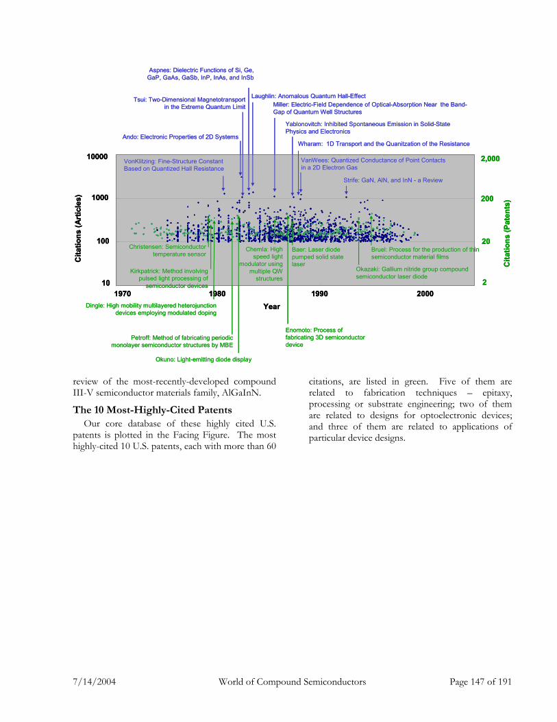
7/14/2004 World of Compound Semiconductors Page 147 of 191
review of the most-recently-developed compound III-V semiconductor materials family, AlGaInN.
The 10 Most-Highly-Cited Patents Our core database of these highly cited U.S.
patents is plotted in the Facing Figure. The most highly-cited 10 U.S. patents, each with more than 60
citations, are listed in green. Five of them are related to fabrication techniques – epitaxy, processing or substrate engineering; two of them are related to designs for optoelectronic devices; and three of them are related to applications of particular device designs.
10
100
1000
10000
1970 1980 1990 2000Year
Cita
tions
(Art
icle
s)
Cita
tions
(Pat
ents
)
20
200
2,000
2
Ando: Electronic Properties of 2D Systems
Laughlin: Anomalous Quantum Hall-Effect
VonKlitzing: Fine-Structure Constant Based on Quantized Hall Resistance
Aspnes: Dielectric Functions of Si, Ge, GaP, GaAs, GaSb, InP, InAs, and InSb
VanWees: Quantized Conductance of Point Contacts in a 2D Electron Gas
Miller: Electric-Field Dependence of Optical-Absorption Near the Band-Gap of Quantum Well Structures
Yablonovitch: Inhibited Spontaneous Emission in Solid-State Physics and Electronics
Tsui: Two-Dimensional Magnetotransportin the Extreme Quantum Limit
Strife: GaN, AlN, and InN - a Review
Bruel: Process for the production of thin semiconductor material films
Enomoto: Process of fabricating 3D semiconductor device
Christensen: Semiconductor temperature sensor
Okuno: Light-emitting diode display
Chemla: High speed light
modulator using multiple QW
structures
Dingle: High mobility multilayered heterojunctiondevices employing modulated doping
Baer: Laser diode pumped solid state laser
Okazaki: Gallium nitride group compound semiconductor laser diode
Kirkpatrick: Method involving pulsed light processing of
semiconductor devices
Petroff: Method of fabricating periodic monolayer semiconductor structures by MBE
Wharam: 1D Transport and the Quanitzation of the Resistance
10
100
1000
10000
1970 1980 1990 2000Year
Cita
tions
(Art
icle
s)
Cita
tions
(Pat
ents
)
20
200
2,000
210
100
1000
10000
1970 1980 1990 2000Year
Cita
tions
(Art
icle
s)
Cita
tions
(Pat
ents
)
20
200
2,000
2
Ando: Electronic Properties of 2D Systems
Laughlin: Anomalous Quantum Hall-Effect
VonKlitzing: Fine-Structure Constant Based on Quantized Hall Resistance
Aspnes: Dielectric Functions of Si, Ge, GaP, GaAs, GaSb, InP, InAs, and InSb
VanWees: Quantized Conductance of Point Contacts in a 2D Electron Gas
Miller: Electric-Field Dependence of Optical-Absorption Near the Band-Gap of Quantum Well Structures
Yablonovitch: Inhibited Spontaneous Emission in Solid-State Physics and Electronics
Tsui: Two-Dimensional Magnetotransportin the Extreme Quantum Limit
Strife: GaN, AlN, and InN - a Review
Bruel: Process for the production of thin semiconductor material films
Enomoto: Process of fabricating 3D semiconductor device
Christensen: Semiconductor temperature sensor
Okuno: Light-emitting diode display
Chemla: High speed light
modulator using multiple QW
structures
Dingle: High mobility multilayered heterojunctiondevices employing modulated doping
Baer: Laser diode pumped solid state laser
Okazaki: Gallium nitride group compound semiconductor laser diode
Kirkpatrick: Method involving pulsed light processing of
semiconductor devices
Petroff: Method of fabricating periodic monolayer semiconductor structures by MBE
Wharam: 1D Transport and the Quanitzation of the Resistance
7/14/2004 World of Compound Semiconductors Page 148 of 191
13.1 Inner-Core Articles by Author
225. G. Abstreiter, M. Cardona, and A. Pinczuk, "Light Scattering in Solids IV: Light-Scattering by Free Carrier Excitations in Semiconductors," Topics in Applied Physics Vol. 54 (1984) 5-150.
358. A.R. Adams, "Band-Structure Engineering for Low-Threshold High-Efficiency Semiconductor-Lasers," Electronics Letters Vol. 22 No. 5 (1986) 249-50.
222. K. Aiki, M. Nakamura, T. Kuroda, J. Umeda, R. Ito, N. Chinone, and M. Maeda, "Transverse Mode Stabilized Alx Ga1-XAs Injection-Lasers Channeled-Substrate-Planar Structure," IEEE Journal of Quantum Electronics Vol. 14 No. 2 (1978) 89-94.
323. I. Akasaki, H. Amano, Y. Koide, K. Hiramatsu, and N. Sawaki, "Effects of AlN Buffer Layer on Crystallographic Structure and on Electrical and Optical-Properties of GaN and Ga1-XAlxN (0 < x <= 0.4) Films Grown on Sapphire Substrate by MOVPE," Journal of Crystal Growth Vol. 98 No. 1-2 (1989) 209-19.
291. O.L. Alerhand, D. Vanderbilt, R.D. Meade, and J.D. Joannopoulos, "Spontaneous Formation of Stress Domains on Crystal-," Physical Review Letters Vol. 61 No. 17 (October 24, 1988) 1973-76.
215. S.J. Allen, D.C. Tsui, and B. Vinter, "ABSORPTION OF INFRARED RADIATION BY ELECTRONS IN SEMICONDUCTOR INVERSION LAYERS," Solid State Communications Vol. 20 No. 4 (1976) 425-28.
579. H. Amano, M. Kito, K. Hiramatsu, and I. Akasaki, "P-Type Conduction in Mg-Doped GaN Treated With Low-Energy Electron-Beam Irradiation (Leebi)," Japanese Journal of Applied Physics Part 2-Letters Vol. 28 No. 12 (1989) L2112-L2114.
538. H. Amano, N. Sawaki, I. Akasaki, and Y. Toyoda, "Metalorganic Vapor-Phase Epitaxial-Growth of a High-Quality GaN Film Using an AlN Buffer Layer," Applied Physics Letters Vol. 48 No. 5 (1986) 353-55.
538. H. Amano, N. Sawaki, I. Akasaki, and Y. Toyoda, "Metalorganic Vapor-Phase Epitaxial-Growth of a High-Quality GaN Film Using an AlN Buffer Layer," Applied Physics Letters Vol. 48 No. 5 (February 3, 1986) 353-55.
248. T. Ando, "Self-Consistent Results for a GaAs/AlxGa1-XAs .2. Low-Temperature Mobility," Journal of the Physical Society of Japan Vol. 51 No. 12 (1982) 3900-3907.
246. T. Ando, "Self-Consistent Results for a GaAs/AlxGa1-XAs .1. Subband Structure and Light-Scattering Spectra," Journal of the Physical Society of Japan Vol. 51 No. 12 (December, 1982) 3893-99.
3080. T. Ando, A.B. Fowler, and F. Stern, "Electronic Properties of Two-Dimensional Systems," Reviews of Modern Physics Vol. 54 No. 2 (April, 1982) 437-672.
210. E.Y. Andrei, G. Deville, D.C. Glattli, F.I.B. Williams, E. Paris, and B. Etienne, "Observation of a Magnetically Induced Wigner Solid," Physical Review Letters Vol. 60 No. 26 (June 27, 1988) 2765-68.
288. R.P. Andres, R.S. Averback, W.L. Brown, L.E. Brus, W.A. Goddard, S.G. Louie, M. Moscovits, P.S. Peercy, S.J. Riley, R.W. Siegel, F. Spaepen, and Y. Wang, "Research Opportunities on Clusters and Cluster-Assembled Materials: a Department of Energy, Council on Materials Science Panel Report," Journal of Materials Research Vol. 4 No. 3 (May, 1989) 704-36.
233. H. Aoki and T. Ando, "Effect of Localization on the Hall Conductivity in the Two-Dimensional System in Strong Magnetic-Fields," Solid State Communications Vol. 38 No. 11 (1981) 1079-82.
891. Y. Arakawa and H. Sakaki, "Multidimensional Quantum Well Laser and Temperature- of Its Threshold Current," Applied Physics Letters Vol. 40 No. 11 (1982) 939-41.
285. Y. Arakawa and A. Yariv, "Quantum-Well Lasers Gain, Spectra, Dynamics," IEEE Journal of Quantum Electronics Vol. 22 No. 9 (1986) 1887-99.
255. M. Asada, A. Kameyama, and Y. Suematsu, "Gain and Intervalence Band Absorption in Quantum-Well," IEEE Journal of Quantum Electronics Vol. 20 No. 7 (1984) 745-53.
294. M. Asada, Y. Miyamoto, and Y. Suematsu, "Gain and the Threshold of 3-Dimensional Quantum-Box Lasers," IEEE Journal of Quantum Electronics Vol. 22 No. 9 (1986) 1915-21.
7/14/2004 World of Compound Semiconductors Page 149 of 191
202. M. Asada and Y. Suematsu, "Density-Matrix Theory of Semiconductor-Lasers With Broadening Model: Gain and Gain-Suppression in Semiconductor-Lasers," IEEE Journal of Quantum Electronics Vol. 21 No. 5 (1985) 434-42.
503. D.J. Ashen, P.J. Dean, D.T.J. Hurle, J.B. Mullin, and A.M. White, "Incorporation and Characterization of Acceptors in Epitaxial GaAs," Journal of Physics and Chemistry of Solids Vol. 36 No. 10 (1975) 1041-53.
244. R.C. Ashoori, "Electrons in Artificial Atoms," Nature Vol. 379 No. 6564 (February 1, 1996) 413-19.
293. R.C. Ashoori, H.L. Stormer, J.S. Weiner, L.N. Pfeiffer, K.W. Baldwin, and K.W. West, "N-Electron Ground-State Energies of a Quantum-Dot in Magnetic-Field," Physical Review Letters Vol. 71 No. 4 (July 26, 1993) 613-16.
495. D.E. Aspnes, "Optical Properties of Thin Films," Thin Solid Films Vol. 89 No. 3 (1982) 249-62.
228. D.E. Aspnes, J.P. Harbison, A.A. Studna, and L.T. Florez, "Application of Reflectance Difference Spectroscopy to Molecular-Beam Epitaxy Growth of GaAs and AlAs," Journal of Vacuum Science & Technology a-Vacuum Films Vol. 6 No. 3 (May, 1988-June 30, 1988) 1327-32.
341. D.E. Aspnes, S.M. Kelso, R.A. Logan, and R. Bhat, "Optical-Properties of AlxGa1-XAs," Journal of Applied Physics Vol. 60 No. 2 (July 15, 1986) 754-67.
1295. D.E. Aspnes and A.A. Studna, "Dielectric Functions and Optical-Parameters of Si, Ge, Gap, GaAs, Gasb, Inp, InAs, and InSb From 1.5 To 6.0 Ev," Physical Review B-Condensed Matter Vol. 27 No. 2 (January 15, 1983) 985-1009.
201. G.B. Bachelet and N.E. Christensen, "Relativistic and Core-Relaxation Effects on the Energy-Bands of Gallium-Arsenide and Germanium," Physical Review B-Condensed Matter Vol. 31 No. 2 (January 15, 1985) 879-87.
208. G.A. Baraff and M. Schluter, "New Self-Consistent Approach to the Electronic-Structure of Localized Defects in Solids," Physical Review B-Condensed Matter Vol. 19 No. 10 (May 15, 1979) 4965-79.
337. G.A. Baraff and M. Schluter, "Electronic-Structure, Total Energies, and Abundances of the
Elementary Point-Defects in GaAs," Physical Review Letters Vol. 55 No. 12 (1985) 1327-30.
212. S.E. Barrett, G. Dabbagh, L.N. Pfeiffer, K.W. West, and R. Tycko, "Optically Pumped Nmr Evidence for Finite-Size Skyrmions in Quantum-Wells Near Landau-Level Filling Nu=1," Physical Review Letters Vol. 74 No. 25 (June 19, 1995) 5112-15.
585. G. Bastard, "Hydrogenic Impurity States in a Quantum Well: a Simple-Model," Physical Review B-Condensed Matter Vol. 24 No. 8 (October 15, 1981) 4714-22.
806. G. Bastard, "Super-Lattice Band-Structure in the Envelope-Function Approximation," Physical Review B-Condensed Matter Vol. 24 No. 10 (November 15, 1981) 5693-97.
469. G. Bastard, "Theoretical Investigations of Super-Lattice Band-Structure in the Envelope-Function Approximation," Physical Review B-Condensed Matter Vol. 25 No. 12 (June 15, 1982) 7584-97.
346. G. Bastard and J.A. Brum, "Electronic States in Semiconductor Heterostructures," IEEE Journal of Quantum Electronics Vol. 22 No. 9 (September, 1986) 1625-44.
220. G. Bastard, J.A. Brum, and R. Ferreira, "Electronic States in Semiconductor Heterostructures," Solid State Physics-Advances in Research and Applications ; Vol. 44 (1991) 230-415.
520. G. Bastard, E.E. Mendez, L.L. Chang, and L. Esaki, "Exciton Binding-Energy in Quantum Wells," Physical Review B-Condensed Matter Vol. 26 No. 4 (August 15, 1982) 1974-79.
457. G. Bastard, E.E. Mendez, L.L. Chang, and L. Esaki, "Variational Calculations on a Quantum Well in an Electric-Field," Physical Review B-Condensed Matter Vol. 28 No. 6 (September 15, 1983) 3241-45.
267. A.R. Beattie and P.T. Landsberg, "Auger Effect in Semiconductors," Proceedings of the Royal Society of London Series a-Mathematical and Physical Sciences Vol. 249 No. 1256 ( 1959) 16-29.
228. P.C. Becker, H.L. Fragnito, C.H.B. Cruz, R.L. Fork, J.E. Cunningham, J.E. Henry, and C.V. Shank, "Femtosecond Photon-Echoes From Band-to-Band Transitions in GaAs," Physical Review Letters Vol. 61 No. 14 (October 3, 1988) 1647-49.
339. C.W.J. Beenakker, "Theory of Coulomb-Blockade Oscillations in the Conductance of a
7/14/2004 World of Compound Semiconductors Page 150 of 191
Quantum Dot," Physical Review B-Condensed Matter Vol. 44 No. 4 (July 15, 1991) 1646-56.
245. C.W.J. Beenakker, "Random-Matrix Theory of Quantum Transport," Reviews of Modern Physics Vol. 69 No. 3 (July, 1997) 731-808.
735. C.W.J. Beenakker and H. Vanhouten, "Quantum Transport in Semiconductor Nanostructures," Solid State Physics-Advances in Research and Applications ; Vol. 44 (1991) 1-229.
368. H. Benisty, C.M. Sotomayortorres, and C. Weisbuch, "Intrinsic Mechanism for the Poor Luminescence Properties of Quantum-Box Systems," Physical Review B-Condensed Matter Vol. 44 No. 19 (November 15, 1991) 10945-48.
215. K.F. Berggren, T.J. Thornton, D.J. Newson, and M. Pepper, "Magnetic Depopulation of 1d Subbands in a Narrow 2d Electron-Gas in a GaAs-AlGaAs Heterojunction," Physical Review Letters Vol. 57 No. 14 (October 6, 1986) 1769-72.
232. F. Bernardini, V. Fiorentini, and D. Vanderbilt, "Spontaneous Polarization and Piezoelectric Constants of III-V Nitrides," Physical Review B-Condensed Matter Vol. 56 No. 16 (October 15, 1997) 10024-27.
217. J. Bernholc and S.T. Pantelides, "Scattering-Theoretic Method for Defects in Semiconductors Tight-Binding Description of Vacancies in Si, Ge, and GaAs," Physical Review B-Condensed Matter Vol. 18 No. 4 (August 15, 1978) 1780-1789.
346. N.E. Bickers, D.J. Scalapino, and S.R. White, "Conserving Approximations for Strongly Correlated Electron-Systems: Bethe-Salpeter-Equation and Dynamics Two-Dimensional Hubbard-Model," Physical Review Letters Vol. 62 No. 8 (February 20, 1989) 961-64.
481. D.K. Biegelsen, R.D. Bringans, J.E. Northrup, and L.E. Swartz, "Surface Reconstructions of GaAs(100) Observed by Scanning Tunneling Microscopy," Physical Review B-Condensed Matter Vol. 41 No. 9 (March 15, 1990) 5701-6.
320. J. Bleuse, G. Bastard, and P. Voisin, "Electric-Field Induced Localization and Oscillatory Electro-Optical Properties of Semiconductor Superlattices," Physical Review Letters Vol. 60 No. 3 (January 18, 1988) 220-223.
320. U. Bockelmann and G. Bastard, "Phonon-Scattering and Energy Relaxation in 2-Dimensional, One-Dimensional, and Zero-Dimensional Electron
Gases," Physical Review B-Condensed Matter Vol. 42 No. 14 (November 15, 1990) 8947-51.
292. D.A. Broido and L.J. Sham, "Effective Masses of Holes at GaAs-AlGaAs Heterojunctions," Physical Review B-Condensed Matter Vol. 31 No. 2 (January 15, 1985) 888-92.
223. E.R. Brown, J.R. Soderstrom, C.D. Parker, L.J. Mahoney, Molvar, and T.C. Mcgill, "Oscillations Up to 712 Ghz in InAs/Alsb Resonant-Tunneling Diodes," Applied Physics Letters Vol. 58 No. 20 (May 20, 1991) 2291-93.
443. F. Capasso, K. Mohammed, and A.Y. Cho, "Resonant Tunneling Through Double Barriers, Perpendicular Quantum Transport Phenomena in Superlattices, and Their Device Applications," IEEE Journal of Quantum Electronics Vol. 22 No. 9 (September, 1986) 1853-69.
212. F. Capasso, W.T. Tsang, A.L. Hutchinson, and G.F. Williams, "Enhancement of Electron-Impact Ionization in a Super-Lattice -a New Avalanche Photo-Diode With a Large Ionization Rate Ratio," Applied Physics Letters Vol. 40 No. 1 (1982) 38-40.
306. M. Cardona, "Light Scattering in Solids II: Resonance Phenomena," Topics in Applied Physics Vol. 50 (1982) 19-178.
319. M. Cardona and N.E. Christensen, "Acoustic Deformation Potentials and Heterostructure Band Offsets in Semiconductors," Physical Review B-Condensed Matter Vol. 35 No. 12 (April 15, 1987) 6182-94.
239. D.J. Chadi, "Spin-Orbit-Splitting in Crystalline and Compositionally Disordered Semiconductors," Physical Review B-Condensed Matter Vol. 16 No. 2 (July 15, 1977) 790-796.
314. D.J. Chadi, "Energy-Minimization Approach to Atomic Geometry of Semiconductor Surfaces," Physical Review Letters Vol. 41 No. 15 (October 9, 1978) 1062-65.
295. D.J. Chadi, "(110) Surface Atomic Structures of Covalent and Ionic Semiconductors," Physical Review B-Condensed Matter Vol. 19 No. 4 (February 15, 1979) 2074-82.
331. D.J. Chadi, "Atomic-Structure of GaAs(100)-(2x1) and GaAs(100)-(2x4) Reconstructed Surfaces," Journal of Vacuum Science & Technology a-Vacuum Films Vol. 5 No. 4 (July, 1987-August 31, 1987) 834-37.
7/14/2004 World of Compound Semiconductors Page 151 of 191
238. D.J. Chadi and K.J. Chang, "Metastability of the Isolated Arsenic-Antisite Defect in GaAs," Physical Review Letters Vol. 60 No. 21 (May 23, 1988) 2187-90.
463. D.J. Chadi and K.J. Chang, "Theory of the Atomic and Electronic-Structure of Dx Centers in GaAs and AlxGa1-XAs Alloys," Physical Review Letters Vol. 61 No. 7 (August 15, 1988) 873-76 .
366. D.J. Chadi and K.J. Chang, "Energetics of Dx-Center Formation in GaAs and AlxGa1-XAs Alloys," Physical Review B-Condensed Matter Vol. 39 No. 14 (May 15, 1989) 10063-74.
308. D.J. Chadi and M.L. Cohen, "Tight-Binding Calculations of Valence Bands of Diamond and Zincblende Crystals," Physica Status Solidi B-Basic Research Vol. 68 No. 1 (1975) 405-19.
314. N. Chand, T. Henderson, J. Klem, W.T. Masselink, R. Fischer, Y.C. Chang, and H. Morkoc, "Comprehensive Analysis of Si-Doped AlxGa1-XAs (x=0 to 1): Theory and Experiments," Physical Review B-Condensed Matter Vol. 30 No. 8 (October 15, 1984) 4481-92.
269. M. Chandrasekhar and F.H. Pollak, "Effects of Uniaxial Stress on the Electroreflectance Spectrum of Ge and GaAs," Physical Review B-Condensed Matter Vol. 15 No. 4 (February 15, 1977) 2127-44.
201. C.C. Chang, P.H. Citrin, and B. Schwartz, "Chemical Preparation of GaAs Surfaces and Their Characterization by Auger-Electron and X-Ray Spectroscopies," Journal of Vacuum Science & Technology Vol. 14 No. 4 (1977) 943-52.
262. D.S. Chemla and D.A.B. Miller, "Room-Temperature Excitonic Nonlinear-Optical Effects in Semiconductor Quantum-Well Structures," Journal of the Optical Society of America B-Optical Physics ; Vol. 2 No. 7 (1985) 1143-53.
492. D.S. Chemla, D.A.B. Miller, P.W. Smith, A.C. Gossard, and W. Wiegmann, "Room-Temperature Excitonic Nonlinear Absorption and Refraction in GaAs/AlGaAs Multiple Quantum Well Structures," IEEE Journal of Quantum Electronics Vol. 20 No. 3 (1984) 265-75.
218. J.T. Cheung and H. Sankur, "Growth of Thin-Films by Laser-Induced Evaporation," CRC Critical Reviews in Solid State and Materials Sciences Vol. 15 No. 1 (1988) 63-109.
230. S. Chichibu, T. Azuhata, T. Sota, and S. Nakamura, "Spontaneous Emission of Localized Excitons in InGaN Single and Multiquantum Well Structures," Applied Physics Letters Vol. 69 No. 27 (December 30, 1996) 4188-90.
202. A.Y. Cho, "Bonding Direction and Surface-Structure Orientation on GaAs (001)," Journal of Applied Physics Vol. 47 No. 7 (1976) 2841-43.
214. K.K. Choi, B.F. Levine, R.J. Malik, J. Walker, and C.G. Bethea, "Periodic Negative Conductance by Sequential Resonant Tunneling Through an Expanding High-Field Superlattice Domain," Physical Review B-Condensed Matter Vol. 35 No. 8 (March 15, 1987) 4172-75.
361. J. Cibert, P.M. Petroff, G.J. Dolan, S.J. Pearton, A.C. Gossard, and J.H. English, "Optically Detected Carrier Confinement to One and Zero Dimension in GaAs Quantum-Well Wires and Boxes," Applied Physics Letters Vol. 49 No. 19 (November 10, 1986) 1275-77.
270. M.E. Coltrin, R.J. Kee, and J.A. Miller, "A Mathematical-Model of the Coupled Fluid-Mechanics and Chemical-Kinetics in a Chemical Vapor-Deposition Reactor," Journal of the Electrochemical Society Vol. 131 No. 2 (1984) 425-34.
338. C. Colvard, T.A. Gant, M.V. Klein, R. Merlin, R. Fischer, H. Morkoc, and A.C. Gossard, "Folded Acoustic and Quantized Optic Phonons in (GaAl)As Superlattices," Physical Review B-Condensed Matter Vol. 31 No. 4 (February 15, 1985) 2080-2091.
216. C. Colvard, R. Merlin, M.V. Klein, and A.C. Gossard, "Observation of Folded Acoustic Phonons in a Semiconductor Super-Lattice," Physical Review Letters Vol. 45 No. 4 (July 28, 1980) 298-301.
233. J. Dabrowski and M. Scheffler, "Theoretical Evidence for an Optically Inducible Structural Transition of the Isolated As Antisite in GaAs - Identification and Explanation of EL2," Physical Review Letters Vol. 60 No. 21 (1988) 2183-86.
200. B. Dahmani, L. Hollberg, and R. Drullinger, "Frequency Stabilization of Semiconductor-Lasers by Resonant Optical Feedback," Optics Letters Vol. 12 No. 11 (1987) 876-78.
250. J.M. Dallesasse, N. Holonyak, A.R. Sugg, T.A. Richard, and N. Elzein, "Hydrolyzation
7/14/2004 World of Compound Semiconductors Page 152 of 191
Oxidation of AlxGa1-XAs-AlAs-GaAs Quantum-Well Heterostructures and Superlattices," Applied Physics Letters Vol. 57 No. 26 (December 24, 1990) 2844-46.
233. R.F. Davis, "III-V Nitrides for Electronic and Optoelectronic Applications," Proceedings of the Ieee Vol. 79 No. 5 (1991) 702-12.
261. P.J. Dean and D.G. Thomas, "Intrinsic Absorption-Edge Spectrum of Gallium Phosphide," Physical Review Vol. 150 No. 2 (1966) 690-703.
266. T. Demel, D. Heitmann, P. Grambow, and K. Ploog, "Nonlocal Dynamic-Response and Level-Crossings in Quantum-Dot Structures," Physical Review Letters Vol. 64 No. 7 (February 12, 1990) 788-91.
322. D.G. Deppe and N. Holonyak, "Atom Diffusion and Impurity-Induced Layer Disordering in Quantum Well III-V Semiconductor Heterostructures," Journal of Applied Physics Vol. 64 No. 12 (December 15, 1988) R93-R113.
210. M.H. Devoret, D. Esteve, H. Grabert, G.L. Ingold, and H. Pothier, "Effect of the Electromagnetic Environment on the Coulomb Blockade in Ultrasmall Tunnel-Junctions," Physical Review Letters Vol. 64 No. 15 (April 9, 1990) 1824-27.
269. R. Dingle, A.C. Gossard, and W. Wiegmann, "Direct Observation of Superlattice Formation in a Semiconductor Heterostructure," Physical Review Letters Vol. 34 No. 21 (May 26, 1975) 1327-30.
789. R. Dingle, H.L. Stormer, A.C. Gossard, and W. Wiegmann, "Electron Mobilities in Modulation-Doped Semiconductor Heterojunction Super-Lattices," Applied Physics Letters Vol. 33 No. 7 (1978) 665-67.
381. A.G. Dirks and H.J. Leamy, "Columnar Microstructure in Vapor-Deposited Thin-Films," Thin Solid Films Vol. 47 No. 3 (1977) 219-33.
321. B.W. Dodson and J.Y. Tsao, "Relaxation of Strained-Layer Semiconductor Structures Via Plastic-Flow," Applied Physics Letters Vol. 51 No. 17 (October 26, 1987) 1325-27.
262. H. Drexler, D. Leonard, W. Hansen, J.P. Kotthaus, and P.M. Petroff, "Spectroscopy of Quantum Levels in Charge-Tunable InGaAs Quantum Dots," Physical Review Letters Vol. 73 No. 16 (October 17, 1994) 2252-55.
527. A.L. Efros and A.L. Efros, "Interband Absorption of Light in a Semiconductor Sphere," Soviet Physics Semiconductors-Ussr Vol. 16 No. 7 (1982 ) 772-75.
1245. R.J. Elliott, "Intensity of Optical Absorption by Excitons," Physical Review Vol. 108 No. 6 ( 1957) 1384-89.
279. L. Esaki, "A Birds-Eye-View on the Evolution of Semiconductor Superlattices and Quantum-Wells," IEEE Journal of Quantum Electronics Vol. 22 No. 9 (1986) 1611-24.
593. J. Faist, F. Capasso, D.L. Sivco, C. Sirtori, A.L. Hutchinson, and A.Y. Cho, "Quantum Cascade Laser," Science Vol. 264 No. 5158 (April 22, 1994) 553-56.
215. S.F. Fang, K. Adomi, S. Iyer, H. Morkoc, H. Zabel, C. Choi, and N. Otsuka, "Gallium-Arsenide and Other Compound Semiconductors on Silicon," Journal of Applied Physics Vol. 68 No. 7 (October 1, 1990) R31-R58.
676. W. Fawcett, A.D. Boardman, and S. Swain, "Monte-Carlo Determination of Electron Transport Properties in Gallium Arsenide," Journal of Physics and Chemistry of Solids Vol. 31 No. 9 ( 1970) 1963-90.
376. R.M. Feenstra, J.A. Stroscio, J. Tersoff, and A.P. Fein, "Atom-Selective Imaging of the GaAs(110) Surface," Physical Review Letters Vol. 58 No. 12 (March 23, 1987) 1192-95.
303. M.M. Fejer, G.A. Magel, D.H. Jundt, and R.L. Byer, "Quasi-Phase-Matched 2nd Harmonic-Generation: Tuning and Tolerances," IEEE Journal of Quantum Electronics Vol. 28 No. 11 2631-54.
503. J. Feldmann, G. Peter, E.O. Gobel, P. Dawson, K. Moore, C. Foxon, and R.J. Elliott, "Linewidth Dependence of Radiative Exciton Lifetimes in Quantum-Wells," Physical Review Letters Vol. 59 No. 20 (November 16, 1987) 2337-40.
295. A.L. Fetter, C.B. Hanna, and R.B. Laughlin, "Random-Phase Approximation in the Fractional-Statistics Gas," Physical Review B-Condensed Matter Vol. 39 No. 13 (May 1, 1989) 9679-81.
210. R.M. Fleming, D.B. Mcwhan, A.C. Gossard, W. Wiegmann, and R.A. Logan, "X-Ray-Diffraction Study of Inter-Diffusion and Growth in (GaAs)N(Aias)M Multilayers," Journal of Applied Physics Vol. 51 No. 1 (1980) 357-63.
7/14/2004 World of Compound Semiconductors Page 153 of 191
238. C.T. Foxon and B.A. Joyce, "Interaction Kinetics of As4 and Ga on [100] GaAs Surfaces Using a Modulated Molecular-Beam Technique," Surface Science Vol. 50 No. 2 (1975) 434-50.
238. C.T. Foxon and B.A. Joyce, "Interaction Kinetics of As2 and Ga on [100] GaAs Surfaces," Surface Science Vol. 64 No. 1 (1977) 293-304.
297. J.L. Freeouf and J.M. Woodall, "Schottky Barriers: an Effective Work Function Model," Applied Physics Letters Vol. 39 No. 9 (1981) 727-29.
436. T.A. Fulton and G.J. Dolan, "Observation of Single-Electron Charging Effects in Small Tunnel-Junctions," Physical Review Letters Vol. 59 No. 1 (July 6, 1987) 109-12.
264. J.M. Gaines, P.M. Petroff, H. Kroemer, R.J. Simes, R.S. Geels, and J.H. English, "Molecular-Beam Epitaxy Growth of Tilted GaAs AlAs Superlattices by Deposition of Fractional Monolayers on Vicinal (001) Substrates," Journal of Vacuum Science & Technology B Vol. 6 No. 4 (July, 1988) 1378-81.
281. R.R. Gerhardts, D. Weiss, and K. Vonklitzing, "Novel Magnetoresistance Oscillations in a Periodically Modulated Two-Dimensional Electron-Gas," Physical Review Letters Vol. 62 No. 10 (March 6, 1989) 1173-76.
324. H.M. Gibbs, S.L. Mccall, T.N.C. Venkatesan , A.C. Gossard, A. Passner, and W. Wiegmann, "Optical Bistability in Semiconductors," Applied Physics Letters Vol. 35 No. 6 (1979) 451-53.
206. H.M. Gibbs, S.S. Tarng, J.L. Jewell, D.A. Weinberger, K. Tai, S.L. Mccall, A. Passner, and W. Wiegmann, "Room-Temperature Excitonic Optical Bistability in a GaAs-GaAlAs Super-Lattice Etalon," Applied Physics Letters Vol. 41 No. 3 (1982) 221-22.
301. S.M. Girvin and A.H. Macdonald, "Off-Diagonal Long-Range Order, Oblique Confinement, and the Fractional Quantum Hall Effect," Physical Review Letters Vol. 58 No. 12 (March 23, 1987) 1252-55.
249. S.M. Girvin, A.H. Macdonald, and P.M. Platzman, "Magneto-Roton Theory of Collective Excitations in the Fractional Quantum Hall-Effect," Physical Review B-Condensed Matter Vol. 33 No. 4 (February 15, 1986) 2481-94.
349. R.W. Godby, M. Schluter, and L.J. Sham, "Self-Energy Operators and Exchange-Correlation Semiconductors," Physical Review B-Condensed Matter Vol. 37 No. 17 (June 15, 1988) 10159-75.
222. K.H. Goetz, D. Bimberg, H. Jurgensen, J. Selders, A.V. Solomonov, G.F. Glinskii, and M. Razeghi, "Optical and Crystallographic Properties and Impurity Incorporation of Gaxin1-Xas (0.44 Less-Than X Less-Than 0.49) Grown by Liquid-Phase Epitaxy, Vapor-Phase Epitaxy, and Organic-Chemical Vapor-Deposition," Journal of Applied Physics Vol. 54 No. 8 (1983) 4543-52.
319. V.J. Goldman, D.C. Tsui, and J.E. Cunningham, "Observation of Intrinsic Bistability in Resonant-Tunneling Structures," Physical Review Letters Vol. 58 No. 12 (March 23, 1987) 1256-59.
347. L. Goldstein, F. Glas, J.Y. Marzin, M.N. Charasse, and G. Leroux, "Growth by Molecular-Beam Epitaxy and Characterization InAs/GaAs Strained-Layer Superlattices," Applied Physics Letters Vol. 47 No. 10 ( November 15, 1985) 1099-101.
305. J.P. Gordon and A. Ashkin, "Motion of Atoms in a Radiation Trap," Physical Review A Vol. 21 No. 5 (1980) 1606-17.
241. U. Gosele and K.N. Tu, "Growth-Kinetics of Planar Binary Diffusion Couples: Thin- Case Versus Bulk Cases," Journal of Applied Physics Vol. 53 No. 4 (1982) 3252-60.
219. R.L. Greene and K.K. Bajaj, "Binding-Energies of Wannier Excitons in GaAs-Ga1-XAlxAs Quantum Well Structures," Solid State Communications Vol. 45 No. 9 (1983) 831-35.
256. R.L. Greene and K.K. Bajaj, "Energy-Levels of Hydrogenic Impurity States in GaAs-Ga1- Quantum Well Structures," Solid State Communications Vol. 45 No. 9 (1983) 825-29.
215. R.L. Greene and K.K. Bajaj, "Effect of Magnetic-Field on the Energy-Levels of a Impurity Center in GaAs Ga1-XAlxAs Quantum-Well Structures," Physical Review B-Condensed Matter Vol. 31 No. 2 (January 15, 1985) 913-18.
348. R.L. Greene, K.K. Bajaj, and D.E. Phelps, "Energy-Levels of Wannier Excitons in GaAs-Ga1-XAlxAs Quantum-Well Structures," Physical Review B-Condensed Matter Vol. 29 No. 4 (February 15, 1984) 1807-12.
418. M. Grundmann, J. Christen, N.N. Ledentsov, J. Bohrer, D. Bimberg, S.S. Ruvimov, P.
7/14/2004 World of Compound Semiconductors Page 154 of 191
Werner, U. Richter, U. Gosele, J. Heydenreich, V.M. Ustinov, A.Y. Egorov, A.E. Zhukov, P.S. Kopev, and Z.I. Alferov, "Ultranarrow Luminescence Lines From Single Quantum Dots," Physical Review Letters Vol. 74 No. 20 (May 15, 1995) 4043-46.
355. M. Grundmann, O. Stier, and D. Bimberg, "Inas/GaAs Pyramidal Quantum Dots - Strain Distribution, Optical Phonons, and Electronic-Structure," Physical Review B-Condensed Matter Vol. 52 No. 16 (October 15, 1995) 11969-81.
239. F.J. Grunthaner, P.J. Grunthaner, R.P. Vasquez, B.F. Lewis, and A. Madhukar, "Local Atomic and Electronic-Structure of Oxide-GaAs and Interfaces Using High-Resolution Xps," Journal of Vacuum Science & Technology Vol. 16 No. 5 1443-53.
385. S. Guha, A. Madhukar, and K.C. Rajkumar, "Onset of Incoherency and Defect Introduction in the Initial-Stages of Molecular-Beam Epitaxial-Growth of Highly Strained InxGa1-XAs on GaAs(100)," Applied Physics Letters Vol. 57 No. 20 (November 12, 1990) 2110-2112.
354. J.B. Gunn, "Instabilities of Current in 3-v Semiconductors," Ibm Journal of Research and Development Vol. 8 No. 2 ( 1964) 141-&.
413. J.B. Gunn, "Microwave Oscillations of Current in III-V Semiconductors," Solid State Communications Vol. 1 No. 4 (1963) 88-91.
231. R.N. Hall, "Solubility of Iii-v Compound Semiconductors in Column-Iii Liquids," Journal of the Electrochemical Society Vol. 110 No. 5 ( 1963) 385-88.
310. R.N. Hall, R.O. Carlson, T.J. Soltys, G.E. Fenner, and J.D. Kingsley, "Coherent Light Emission From Gaas Junctions," Physical Review Letters Vol. 9 No. 9 ( 1962) 366-69.
484. R.N. Hall and J.H. Racette, "Diffusion + Solubility of Copper in Extrinsic + Intrinsic Germanium Silicon + Gallium Arsenide," Journal of Applied Physics Vol. 35 No. 2 ( 1964) 379-97.
204. E. Hanamura and H. Haug, "Condensation Effects of Excitons," Physics Reports-Review Section of Physics Letters Vol. 33 No. 4 (1977) 209-84.
244. W. Hansen, M. Horst, J.P. Kotthaus, U. Merkt, C. Sikorski, and K. Ploog, "Intersubband Resonance in Quasi One-Dimensional Inversion
Channels," Physical Review Letters Vol. 58 No. 24 (June 15, 1987) 2586-89.
235. J.J. Harris, B.A. Joyce, and P.J. Dobson, "Oscillations in the Surface-Structure of Sn-Doped GaAs Growth by MBE," Surface Science Vol. 103 No. 1 (1981) L90-L96.
271. W.A. Harrison, "Surface Reconstruction on Semiconductors," Surface Science Vol. 55 No. 1 (1976) 1-19.
382. W.A. Harrison, "Elementary Theory of Heterojunctions," Journal of Vacuum Science & Technology Vol. 14 No. 4 (1977) 1016-21.
209. W.A. Harrison, "New Tight-Binding Parameters for Covalent Solids Obtained Louie Peripheral States," Physical Review B-Condensed Matter Vol. 24 No. 10 (November 15, 1981) 5835-43.
244. W.A. Harrison, E.A. Kraut, J.R. Waldrop, and R.W. Grant, "Polar Heterojunction Interfaces," Physical Review B-Condensed Matter Vol. 18 No. 8 (October 15, 1978) 4402-10.
201. W.A. Harrison and J. Tersoff, "Tight-Binding Theory of Heterojunction Band Lineups and Interface Dipoles," Journal of Vacuum Science & Technology B Vol. 4 No. 4 (July, 1986-August 31, 1986) 1068-73.
364. H. Haug and S. Schmittrink, "Electron Theory of the Optical-Properties of Laser-Excited Semiconductors," Progress in Quantum Electronics Vol. 9 No. 1 (1984) 3-100.
530. J.W. Haus and K.W. Kehr, "Diffusion in Regular and Disordered Lattices," Physics Reports-Review Section of Physics Letters Vol. 150 No. 5-6 263-406.
245. M. Heiblum, M.I. Nathan, D.C. Thomas, and C.M. Knoedler, "Direct Observation of Ballistic Transport in GaAs," Physical Review Letters Vol. 55 No. 20 (November 11, 1985) 2200-2203.
795. C.H. Henry, "Theory of the Linewidth of Semiconductor-Lasers," IEEE Journal of Quantum Electronics Vol. 18 No. 2 (1982) 259-64.
214. C.H. Henry, "Theory of Spontaneous Emission Noise in Open Resonators Application to Lasers and Optical Amplifiers," Journal of Lightwave Technology Vol. 4 No. 3 (1986) 288-97.
640. C.H. Henry and D.V. Lang, "Nonradiative Capture and Recombination by Multiphonon Emission in GaAs and GaP," Physical Review B-
7/14/2004 World of Compound Semiconductors Page 155 of 191
Condensed Matter Vol. 15 No. 2 (January 15, 1977) 989-1016.
262. C. Hermann and C. Weisbuch, "K.p Perturbation-Theory in III-V Compounds and Alloys: Re-Examination," Physical Review B-Condensed Matter Vol. 15 No. 2 (January 15, 1977) 823-33.
280. H.F. Hess, E. Betzig, T.D. Harris, L.N. Pfeiffer, and K.W. West, "Near-Field Spectroscopy of the Quantum Constituents of a Luminescent System," Science Vol. 264 No. 5166 (June 17, 1994) 1740-1745.
215. K. Hess, "Impurity and Phonon-Scattering in Layered Structures," Applied Physics Letters Vol. 35 No. 7 (1979) 484-86.
226. K. Hess, H. Morkoc, H. Shichijo, and B.G. Streetman, "Negative Differential Resistance Through Real-Space Electron-Transfer," Applied Physics Letters Vol. 35 No. 6 (1979) 469-71.
382. H.P. Hjalmarson, P. Vogl, D.J. Wolford, and J.D. Dow, "Theory of Substitutional Deep Traps in Covalent Semiconductors," Physical Review Letters Vol. 44 No. 12 (March 24, 1980) 810-813.
454. K.M. Ho, C.T. Chan, and C.M. Soukoulis, "Existence of a Photonic Gap in Periodic Dielectric Structures," Physical Review Letters Vol. 65 No. 25 (December 17, 1990) 3152-55.
264. D.E. Holmes, R.T. Chen, K.R. Elliott, and C.G. Kirkpatrick, "Stoichiometry-Controlled Compensation in Liquid Encapsulated Czochralski GaAs," Applied Physics Letters Vol. 40 No. 1 (1982) 46-48.
397. N. Holonyak, R.M. Kolbas, R.D. Dupuis, and P.D. Dapkus, "Quantum-Well Heterostructure Lasers," IEEE Journal of Quantum Electronics Vol. 16 No. 2 (1980) 170-186.
275. J.J. Hopfield, D.G. Thomas, and R.T. Lynch, "Isoelectronic Donors and Acceptors," Physical Review Letters Vol. 17 (August 8, 1966) 312-16.
255. Y. Horikoshi, M. Kawashima, and H. Yamaguchi, "Low-Temperature Growth of GaAs and AlAs-GaAs Quantum- Layers by Modified Molecular-Beam Epitaxy," Japanese Journal of Applied Physics Part 2-Letters Vol. 25 No. 10 L68-L70.
204. Y. Horikoshi, M. Kawashima, and H. Yamaguchi, "Migration-Enhanced Epitaxy of GaAs
and AlGaAs," Japanese Journal of Applied Physics Part 1-Regular Papers & Short Notes Vol. 27 No. 2 (1988) 169-79.
243. K. Huang and B.F. Zhu, "Dielectric Continuum Model and Frohlich Interaction in Superlattices," Physical Review B-Condensed Matter Vol. 38 No. 18 (1988) 13377-86.
215. D.L. Huffaker, D.G. Deppe, K. Kumar, and T.J. Rogers, "Native-Oxide Defined Ring Contact for Low-Threshold Vertical-Cavity Lasers," Applied Physics Letters Vol. 65 No. 1 (July 4, 1994) 97-99.
380. M.S. Hybertsen and S.G. Louie, "1st-Principles Theory of Quasiparticles: Calculation of Band-Gaps in Semiconductors and Insulators," Physical Review Letters Vol. 55 No. 13 (September 23, 1985) 1418-21.
309. K. Iga, F. Koyama, and S. Kinoshita, "Surface Emitting Semiconductor-Lasers," IEEE Journal of Quantum Electronics Vol. 24 No. 9 (September, 1988) 1845-55.
860. J. Ihm, A. Zunger, and M.L. Cohen, "Momentum-Space Formalism for the Total Energy of Solids," Journal of Physics C-Solid State Physics Vol. 12 No. 21 (November 14, 1979) 4409-22.
251. R.A. Jalabert, H.U. Baranger, and A.D. Stone, "Conductance Fluctuations in the Ballistic Regime: a Probe of Quantum Chaos," Physical Review Letters Vol. 65 No. 19 (November 5, 1990) 2442-45.
261. J.L. Jewell, J.P. Harbison, A. Scherer, Y.H. Lee, and L.T. Florez, "Vertical-Cavity Surface-Emitting Lasers: Design, Growth, Fabrication, Characterization," IEEE Journal of Quantum Electronics Vol. 27 No. 6 (June, 1991) 1332-46.
252. J.D. Joannopoulos, P.R. Villeneuve, and S.H. Fan, "Photonic Crystals: Putting a New Twist on Light," Nature Vol. 386 No. 6621 (March 13, 1997) 143-49.
607. S. John, "Strong Localization of Photons in Certain Disordered Dielectric Superlattices," Physical Review Letters Vol. 58 No. 23 (June 8, 1987) 2486-89.
262. A.S. Jordan, R. Caruso, and A.R. Vonneida, "A Thermoelastic Analysis of Dislocation Generation in GaAs Crystals," Bell System Technical Journal Vol. 59 No. 4 (1980) 593-637.
299. B. Jusserand and M. Cardona, "Light Scattering in Solids V: Raman-Spectroscopy of
7/14/2004 World of Compound Semiconductors Page 156 of 191
Vibrations in Superlattices," Topics in Applied Physics Vol. 66 (1989) 49-152.
409. V. Kalmeyer and R.B. Laughlin, "Equivalence of the Resonating-Valence-Bond and Quantum Hall States," Physical Review Letters Vol. 59 No. 18 (1987) 2095-98.
287. M. Kaminska, Liental WZ, E. Weber, T. George, J. Kortright, F. Smith, B.Y. Tsaur, and A.R. Calawa, "Structureal-Properties of As Rich GaAs Grown by Molecular Beam Epitaxy at Low Temperatures," Applied Physics Letters Vol. 54 No. 19 (1989) 1881-83.
209. I. Kamiya, D.E. Aspnes, L.T. Florez, and J.P. Harbison, "Reflectance-Difference Spectroscopy of (001) GaAs-Surfaces Ultrahigh-Vacuum," Physical Review B-Condensed Matter Vol. 46 No. 24 (December 15, 1992) 15894-904.
333. C.L. Kane and M.P.A. Fisher, "Transport in a One-Channel Luttinger Liquid," Physical Review Letters Vol. 68 No. 8 (February 24, 1992) 1220-1223.
365. C.L. Kane and M.P.A. Fisher, "Transmission Through Barriers and Resonant Tunneling in an Interacting One-Dimensional Electron Gas," Physical Review B-Condensed Matter Vol. 46 No. 23 (December 15, 1992) 15233-62.
432. E. Kapon, D.M. Hwang, and R. Bhat, "Stimulated-Emission in Semiconductor Quantum Wire Heterostructures," Physical Review Letters Vol. 63 No. 4 (July 24, 1989) 430-433.
236. J.A. Kash, J.C. Tsang, and J.M. Hvam, "Subpicosecond Time-Resolved Raman Spectroscopy of Lo Phonons in GaAs," Physical Review Letters Vol. 54 No. 19 (May 13, 1985) 2151-54.
231. K. Kash, A. Scherer, J.M. Worlock, H.G. Craighead, and M.C. Tamargo, "Optical Spectroscopy of Ultrasmall Structures Etched From Quantum-Wells," Applied Physics Letters Vol. 49 No. 16 (October 20, 1986) 1043-45.
225. L.C. Kimerling, "Recombination Enhanced Defect Reactions," Solid-State Electronics Vol. 21 No. 11-1 (1978) 1391-401.
285. N. Kirstaedter, N.N. Ledentsov, M. Grundmann, D. Bimberg, S.S. Ruvimov, M.V. Maximov, P.S. Kopev, Z.I. Alferov, U. Richter, P. Werner, U. Gosele, and J. Heydenreich, "Low-Threshold, Large T-O Injection-Laser Emission
From (Inga)As Quantum Dots," Electronics Letters Vol. 30 No. 17 (August 18, 1994) 1416-17.
285. M.V. Klein, "Phonons in Semiconductor Superlattices," IEEE Journal of Quantum Electronics Vol. 22 No. 9 (1986) 1760-1770.
316. C. Klingshirn and H. Haug, "Optical-Properties of Highly Excited Direct Gap," Physics Reports-Review Section of Physics Letters Vol. 70 No. 5 .316-98.
248. W.H. Knox, C. Hirlimann, D.A.B. Miller, J. Shah, D.S. Chemla, and C.V. Shank, "Femtosecond Excitation of Nonthermal Carrier Populations GaAs Quantum-Wells," Physical Review Letters Vol. 56 No. 11 (March 17, 1986) 1191-93.
266. S. Kobayashi, Y. Yamamoto, M. Ito, and T. Kimura, "Direct Frequency-Modulation in AlGaAs Semiconductor-," IEEE Journal of Quantum Electronics Vol. 18 No. 4 (1982) 582-95.
219. K. Kohler, J.W. Coburn, D.E. Horne, E. Kay, and J.H. Keller, "Plasma Potentials of 13.56-Mhz Rf Argon Glow-Discharges in a Planar System," Journal of Applied Physics Vol. 57 No. 1 (January 1, 1985) 59-66.
234. B. Kramer and A. Mackinnon, "Localization: Theory and Experiment," Reports on Progress in Physics Vol. 56 No. 12 (December, 1993) 1469-564.
539. H. Kroemer, "Heterostructure Bipolar-Transistors and Integrated-Cirucuts," Proceedings of the IEEE Vol. 70 No. 1 (1982) 13-25.
273. H. Kroemer, W.Y. Chien, J.S. Harris, and D.D. Edwall, "Measurement of Isotype Heterojunction Barriers by C-V Profiling," Applied Physics Letters Vol. 36 No. 4 (1980) 295-97.
281. T.S. Kuan, T.F. Kuech, W.I. Wang, and E.L. Wilkie, "Long-Range Order in AlxGa1-XAs," Physical Review Letters Vol. 54 No. 3 (January 21, 1985) 201-4.
269. A. Kumar, S.E. Laux, and F. Stern, "Electron-States in a GaAs Quantum Dot in a Magnetic-Field," Physical Review B-Condensed Matter Vol. 42 No. 8 (September 15, 1990) 5166-75.
247. J. Lagowski, H.C. Gatos, J.M. Parsey, K. Wada, M. Kaminska, and W. Walukiewicz, "Origin of the 0.82-Ev Electron Trap in GaAs and Its Annihilation by Shallow Donors," Applied Physics Letters Vol. 40 No. 4 (1982) 342-44.
403. W.D. Laidig, N. Holonyak, M.D. Camras, K. Hess, J.J. Coleman, and J. Bardeen, "Disorder of
7/14/2004 World of Compound Semiconductors Page 157 of 191
an AlAs-GaAs Super-Lattice by Impurity Diffusion," Applied Physics Letters Vol. 38 No. 10 (1981) 776-78.
307. D.V. Lang and R.A. Logan, "Study of Deep Levels in GaAs by Capacitance Spectroscopy," Journal of Electronic Materials Vol. 4 No. 5 (1975) 1053-66.
422. D.V. Lang and R.A. Logan, "Large-Lattice-Relaxation Model for Persistent Photoconductivity in Compound Semiconductors," Physical Review Letters Vol. 39 No. 10 ( September 5, 1977) 635-39.
658. D.V. Lang, R.A. Logan, and M. Jaros, "Trapping Characteristics and a Donor-Complex (DX) Model for the Persistent Photoconductivity Trapping Center in Te-Doped AlxGa1-XAs," Physical Review B-Condensed Matter Vol. 19 No. 2 (January 15, 1979) 1015-30.
618. R.B. Laughlin, "Quantized Hall Conductivity in 2 Dimensions," Physical Review B-Condensed Matter Vol. 23 No. 10 (May 15, 1981) 5632-33.
1400. R.B. Laughlin, "Anomalous Quantum Hall-Effect: an Incompressible Quantum Fluid With Fractionally Charged Excitations," Physical Review Letters Vol. 50 No. 18 (May 2, 1983) 1395-98.
394. R.B. Laughlin, "The Relationship Between High-Temperature the Fractional Quantum Hall-Effect," Science Vol. 242 No. 4878 (1988) 525-33.
249. P. Lautenschlager, M. Garriga, S. Logothetidis, and M. Cardona, "Interband Critical-Points of GaAs and Their Temperature-Dependence," Physical Review B-Condensed Matter Vol. 35 No. 17 (June 15, 1987) 9174-89.
244. S.E. Laux, D.J. Frank, and F. Stern, "Quasi-One-Dimensional Electron-States in a Split-Gate GaAs/AlGaAs Heterostructure," Surface Science Vol. 196 No. 1-3 (1988) 101-6.
261. C.S. Lent and P.I. Cohen, "Diffraction From Stepped Surfaces .1. Reversible Surfaces," Surface Science Vol. 139 No. 1 (1984) 121-54.
795. D. Leonard, M. Krishnamurthy, C.M. Reaves, and S.P. Denbaars, "Direct Formation of Quantum-Sized Dots From Uniform Coherent Islands of InGaAs on GaAs-Surfaces," Applied Physics Letters Vol. 63 No. 23 (December 6, 1993) 3203-5.
435. D. Leonard, K. Pond, and P.M. Petroff, "Critical Layer Thickness for Self-Assembled InAs
Islands on GaAs," Physical Review B-Condensed Matter Vol. 50 No. 16 (October 15, 1994) 11687-92.
312. S.D. Lester, F.A. Ponce, M.G. Craford, and D.A. Steigerwald, "High Dislocation Densities in High-Efficiency GaN-Based Light-Emitting-Diodes," Applied Physics Letters Vol. 66 No. 10 (March 6, 1995) 1249-51.
228. K.M. Leung and Y.F. Liu, "Full Vector Wave Calculation of Photonic Band Structures in Face-Centered-Cubic Dielectric Media," Physical Review Letters Vol. 65 No. 21 (November 19, 1990) 2646-49.
483. B.F. Levine, "Quantum-Well Infrared Photodetectors," Journal of Applied Physics Vol. 74 No. 8 (October 15, 1993) R1-R81.
297. B.F. Levine, K.K. Choi, C.G. Bethea, J. Walker, and R.J. Malik, "New 10 Mu-M Infrared Detector Using Intersubband Absorption in Resonant Tunneling GaAlAs Superlattices," Applied Physics Letters Vol. 50 No. 16 (April 20, 1987) 1092-94.
228. B.F. Levine, R.J. Malik, J. Walker, K.K. Choi, C.G. Bethea, D.A. Kleinman, and J.M. Vandenberg, "Strong 8.2 Mu-M Infrared Intersubband Absorption in Doped GaAs/AlAs Quantum-Well Wave-Guides," Applied Physics Letters Vol. 50 No. 5 (February 2, 1987) 273-75.
275. M. Lindberg and S.W. Koch, "Effective Bloch Equations for Semiconductors," Physical Review B-Condensed Matter Vol. 38 No. 5 (August 15, 1988 ) 3342-50.
219. M.A. Littlejohn, J.R. Hauser, and T.H. Glisson, "Velocity-Field Characteristics of GaAs With Gamma-6(C)-L6(C)-X6(C) Conduction-Band Ordering," Journal of Applied Physics Vol. 48 No. 11 (1977) 4587-90.
201. S.G. Louie, J.R. Chelikowsky, and M.L. Cohen, "Ionicity and Theory of Schottky Barriers," Physical Review B-Condensed Matter Vol. 15 No. 4 (February 15, 1977) 2154-62.
229. M.J. Ludowise, "Metalorganic Chemical Vapor Deposition of III-V Semiconductors," Journal of Applied Physics Vol. 58 No. 8 (October 15, 1985) R31-R55.
327. S. Luryi, "Frequency Limit of Double-Barrier Resonant-Tunneling Oscillators," Applied Physics Letters Vol. 47 No. 5 (September 1, 1985) 490-492.
7/14/2004 World of Compound Semiconductors Page 158 of 191
1549. J.M. Luttinger and W. Kohn, "Motion of Electrons and Holes in Perturbed Periodic Fields," Physical Review Vol. 97 (1955) 869-83.
249. S. Machida, Y. Yamamoto, and Y. Itaya, "Observation of Amplitude Squeezing in a Constant-Current Semiconductor-Laser," Physical Review Letters Vol. 58 No. 10 (March 9, 1987) 1000-1003.
273. C. Mailhiot, Y.C. Chang, and T.C. Mcgill, "Energy-Spectra of Donors in GaAs-Ga1-XAlxAs Quantum Well Structures in the Effective-Mass Approximation," Physical Review B-Condensed Matter Vol. 26 No. 8 (October 15, 1982) 4449-57 .
233. C. Mailhiot, C.B. Duke, and D.J. Chadi, "Sb Overlayers on (110) Surfaces of III-V-Semiconductors: Total-Energy Minimization and Surface Electronic-Structure," Physical Review B-Condensed Matter Vol. 31 No. 4 (February 15, 1985) 2213-29.
302. C.M. Marcus, A.J. Rimberg, R.M. Westervelt , P.F. Hopkins, and Gossard, "Conductance Fluctuations and Chaotic Scattering in Ballistic Microstructures," Physical Review Letters Vol. 69 No. 3 (July 20, 1992) 506-9.
264. P.M.J. Maree, J.C. Barbour, J.F. Vanderveen, K.L. Kavanagh, C.W.T. Bullelieuwma, and M.P.A. Viegers, "Generation of Misfit Dislocations in Semiconductors," Journal of Applied Physics Vol. 62 No. 11 (December 1, 1987) 4413-20.
374. W.C. Marra, P. Eisenberger, and A.Y. Cho, "X-Ray Total-External-Reflection-Bragg Diffraction - Structural Study of the GaAs-Al Interface," Journal of Applied Physics Vol. 50 No. 11 (1979) 6927-33.
404. G.M. Martin, "Optical Assessment of the Main Electron Trap in Bulk Semi-Insulating GaAs," Applied Physics Letters Vol. 39 No. 9 (1981) 747-48.
542. G.M. Martin, A. Mitonneau, and A. Mircea, "Electron Traps in Bulk and Epitaxial GaAs Crystals," Electronics Letters Vol. 13 No. 7 (1977) 191-93.
228. J.L. Martins and A. Zunger, "Bond Lengths Around Isovalent Impurities and in Semiconductor Solid-Solutions," Physical Review B-Condensed Matter Vol. 30 No. 10 ( November 15, 1984) 6217-20.
562. J.Y. Marzin, J.M. Gerard, A. Izrael, D. Barrier, and G. Bastard, "Photoluminescence of Single InAs Quantum Dots Obtained by Self-Organized Growth on GaAs," Physical Review Letters Vol. 73 No. 5 (August 1, 1994) 716-19.
256. P.L. Mceuen, E.B. Foxman, U. Meirav, M.A. Kastner, Y. Meir, and S.J. Wind, "Transport Spectroscopy of a Coulomb Island in the Quantum Regime," Physical Review Letters Vol. 66 No. 14 (April 8, 1991) 1926-29.
247. Y. Meir, N.S. Wingreen, and P.A. Lee, "Transport Through a Strongly Interacting Electron-System: Theory of Periodic Conductance Oscillations," Physical Review Letters Vol. 66 No. 23 (June 10, 1991) 3048-51.
548. E.E. Mendez, F. Agullorueda, and J.M. Hong, "Stark Localization in GaAs-GaAlAs Superlattices Under an Electric-Field," Physical Review Letters Vol. 60 No. 23 (June 6, 1988) 2426-29.
229. E.E. Mendez, G. Bastard, L.L. Chang, L. Esaki, H. Morkoc, and R. Fischer, "Effect of an Electric-Field on the Luminescence of GaAs Quantum Wells," Physical Review B-Condensed Matter Vol. 26 No. 12 (December 15, 1982) 7101-4.
488. R. Merlin, K. Bajema, R.G. Clarke, F.Y. Juang, and P.K. Bhattacharya, "Quasiperiodic GaAs-AlAs Heterostructures," Physical Review Letters Vol. 55 No. 17 (October 21, 1985) 1768-70.
403. D.A.B. Miller, D.S. Chemla, T.C. Damen, A.C. Gossard, W. Wiegmann, T.H. Wood, and C.A. Burrus, "Novel Hybrid Optically Bistable Switch: the Quantum Well Self-Electro-Optic Effect Device," Applied Physics Letters Vol. 45 No. 1 (1984) 13-15.
602. D.A.B. Miller, D.S. Chemla, T.C. Damen, A.C. Gossard, W. Wiegmann, T.H. Wood, and C.A. Burrus, "Band-Edge Electroabsorption in Quantum Well Structures: the Quantum-Confined Stark-Effect," Physical Review Letters Vol. 53 No. 22 (November 26, 1984) 2173-76.
1120. D.A.B. Miller, D.S. Chemla, T.C. Damen, A.C. Gossard, W. Wiegmann, T.H. Wood, and C.A. Burrus, "Electric-Field Dependence of Optical-Absorption Near the Band-Gap of Quantum-Well Structures," Physical Review B-Condensed Matter Vol. 32 No. 2 (July 15, 1985) 1043-60.
372. D.A.B. Miller, D.S. Chemla, T.C. Damen, T.H. Wood, C.A. Burrus, and W. Wiegmann, "The
7/14/2004 World of Compound Semiconductors Page 159 of 191
Quantum Well Self-Electrooptic Effect Device: Optoelectronic Bistability and Oscillation, and Self- Modulation," IEEE Journal of Quantum Electronics Vol. 21 No. 9 (1985) 1462-76.
283. D.A.B. Miller, D.S. Chemla, D.J. Eilenberger, P.W. Smith, A.C. Gossard, and W.T. Tsang, "Large Room-Temperature Optical Nonlinearity in GaAs/Ga1-X Alxas Multiple Quantum Well Structures," Applied Physics Letters Vol. 41 No. 8 (1982) 679-81.
205. D.A.B. Miller, C.T. Seaton, M.E. Prise, and S.D. Smith, "Band-Gap-Resonant Non-Linear Refraction in III-V Semiconductors," Physical Review Letters Vol. 47 No. 3 (1981) 197-200.
267. D.A.B. Miller, S.D. Smith, and A. Johnston, "Optical Bistability and Signal Amplification in a Semiconductor Crystal - Applications of New Low-Power Non-Linear Effects in InSb," Applied Physics Letters Vol. 35 No. 9 (1979) 658-60.
215. D.A.B. Miller, J.S. Weiner, and D.S. Chemla, "Electric-Field Dependence of Linear Optical-Properties in Quantum-Well Structures: Wave-Guide Electroabsorption Sum-Rules," IEEE Journal of Quantum Electronics Vol. 22 No. 9 (September, 1986) 1816-30.
287. R.C. Miller, A.C. Gossard, D.A. Kleinman, and O. Munteanu, "Parabolic Quantum Wells With the GaAs-AlxGa1-XAs System," Physical Review B-Condensed Matter Vol. 29 No. 6 (March 15, 1984) 3740-3743.
233. R.C. Miller, A.C. Gossard, W.T. Tsang, and O. Munteanu, "Extrinsic Photo-Luminescence From GaAs Quantum Wells," Physical Review B-Condensed Matter Vol. 25 No. 6 (March 15, 1982) 3871-77.
204. R.C. Miller and D.A. Kleinman, "Excitons in GaAs Quantum Wells," Journal of Luminescence Vol. 30 No. 1-4 (1985) 520-540.
541. R.C. Miller, D.A. Kleinman, and A.C. Gossard, "Energy-Gap Discontinuities and Effective Masses for GaAs-AlxGa1-XAs Quantum Wells," Physical Review B-Condensed Matter Vol. 29 No. 12 (June 15, 1984) 7085-87.
226. R.C. Miller, D.A. Kleinman, W.A. Nordland, and A.C. Gossard, "Luminescence Studies of Optically Pumped Quantum Wells in GaAs-AlxGa1-XAs Multilayer Structures," Physical Review B-Condensed Matter Vol. 22 No. 2 (July 15, 1980) 863-71.
360. R.C. Miller, D.A. Kleinman, W.T. Tsang, and A.C. Gossard, "Observation of the Excited-Level of Excitons in GaAs Wells," Physical Review B-Condensed Matter Vol. 24 No. 2 (July 15, 1981) 1134-36.
420. T. Mimura, S. Hiyamizu, T. Fujii, and K. Nanbu, "A New Field-Effect Transistor With Selectively Doped GaAs-N-AlxGa1-XAs Heterojunctions," Japanese Journal of Applied Physics Vol. 19 No. 5 (1980) L225-L227.
219. A. Mitonneau, G.M. Martin, and A. Mircea, "Hole Traps in Bulk and Epitaxial GaAs Crystals," Electronics Letters Vol. 13 No. 22 (1977) 666-68.
230. M. Mizuta, M. Tachikawa, H. Kukimoto, and S. Minomura, "Direct Evidence for the DX Center Being a Substitutional Donor in AlGaAs Alloy System," Japanese Journal of Applied Physics Part 2-Letters Vol. 24 No. 2 (1985) L143-L146.
248. S.N. Mohammad, A. Salvador, and H. Morkoc, "Emerging Gallium Nitride Based Devices," Proceedings of the IEEE Vol. 83 No. 10 (October, 1995) 1306-55.
524. P.M. Mooney, "Deep Donor Levels (Dx Centers) in III-V Semiconductors," Journal of Applied Physics Vol. 67 No. 3 (February 1, 1990) R1-R26.
326. N. Mori and T. Ando, "Electron Optical-Phonon Interaction in Single and Double Heterostructures," Physical Review B-Condensed Matter Vol. 40 No. 9 (September 15, 1989) 6175-88.
912. H. Morkoc, S. Strite, G.B. Gao, M.E. Lin, B. Sverdlov, and M. Burns, "Large-Band-Gap SiC, III-V Nitride, and II-VI ZnSe-Based Semiconductor-Device Technologies," Journal of Applied Physics Vol. 76 No. 3 (August 1, 1994) 1363-98.
269. A. Mysyrowicz, D. Hulin, A. Antonetti, and A. Migus, "Dressed Excitons in a Multiple-Quantum-Well Structure: Evidence for an Optical Stark-Effect With Femtosecond Response-Time," Physical Review Letters Vol. 56 No. 25 (June 23, 1986) 2748-51.
239. R.E. Nahory, M.A. Pollack, W.D. Johnston, and R.L. Barns, "Band-Gap Versus Composition and Demonstration of Vegards Law for In1-XGaxAsyP1-y Lattice Matched to InP," Applied Physics Letters Vol. 33 No. 7 (1978) 659-61.
435. S. Nakamura, "GaN Growth Using GaN Buffer Layer," Japanese Journal of Applied Physics
7/14/2004 World of Compound Semiconductors Page 160 of 191
Part 2-Letters Vol. 30 No. 10a ( October, 1991) L1705-L1707.
328. S. Nakamura, N. Iwasa, M. Senoh, and T. Mukai, "Hole Compensation Mechanism of P-Type GaN Films," Japanese Journal of Applied Physics Part 1-Regular Papers Notes & Review Papers Vol. 31 No. 5a (May, 1992) 1258-66.
261. S. Nakamura, T. Mukai, and M. Senoh, "High-Power GaN P-N-Junction Blue-Light-Emitting Diodes," Japanese Journal of Applied Physics Part 2-Letters Vol. 30 No. 12A (December 1, 1991) L1998-L2001.
811. S. Nakamura, T. Mukai, and M. Senoh, "Candela-Class High-Brightness InGaN/AlGaN Double-Heterostructure Blue-Light-Emitting Diodes," Applied Physics Letters Vol. 64 No. 13 (March 28, 1994) 1687-89.
301. S. Nakamura, M. Senoh, N. Iwasa, S. Nagahama, T. Yamada, and T. Mukai, "Superbright Green InGaN Single-Quantum-Well-Structure Light-Emitting-Diodes," Japanese Journal of Applied Physics Part 2-Letters Vol. 34 No. 10B (October 15, 1995) L1332-L1335.
895. S. Nakamura, M. Senoh, S. Nagahama, N. Iwasa, T. Yamada, T. Matsushita, H. Kiyoku, and Y. Sugimoto, "InGaN-Based Multi-Quantum-Well-Structure Laser Diodes," Japanese Journal of Applied Physics Part 2-Letters Vol. 35 No. 1B (January 15, 1996) L74-L76.
212. S. Nakamura, M. Senoh, S. Nagahama, N. Iwasa, T. Yamada, T. Matsushita, H. Kiyoku, Y. Sugimoto, T. Kozaki, H. Umemoto, M. Sano , and K. Chocho, "InGaN/Gan/AlGaN-Based Laser Diodes With Modulation-Doped Strained-Layer Superlattices Grown on an Epitaxially Laterally Overgrown GaN Substrate," Applied Physics Letters Vol. 72 No. 2 (January 12, 1998) 211-13.
389. S. Nakamura, N. Senoh, N. Iwasa, and S. Nagahama, "High-Brightness InGaN Blue, Green and Yellow Light-Emitting-Diodes With Quantum-Well Structures," Japanese Journal of Applied Physics Part 2-Letters Vol. 34 No. 7A (July 1, 1995) L797-L799.
273. Y. Narukawa, Y. Kawakami, M. Funato, S. Fujita, S. Fujita, and S. Nakamura, "Role of Self-Formed InGaN Quantum Dots for Exciton Localization in the Purple Laser Diode Emitting at 420 Nm," Applied Physics Letters Vol. 70 No. 8 (February 24, 1997) 981-83.
270. M.I. Nathan, W.P. Dumke, G. Burns, F.H. Dill, and G. Lasher, "Stimulated Emission of Radiation From Gaas P-n Junctions," Applied Physics Letters Vol. 1 No. 3 ( 1962) 62-64.
492. J.H. Neave, P.J. Dobson, B.A. Joyce, and J. Zhang, "Reflection High-Energy Electron-Diffraction Oscillations From Vicinal Surfaces - a New Approach to Surface-Diffusion Measurements," Applied Physics Letters Vol. 47 No. 2 (July 15, 1985) 100-102.
692. J.H. Neave, B.A. Joyce, P.J. Dobson, and N. Norton, "Dynamics of Film Growth of GaAs by MBE From RHEED Observations," Applied Physics a-Solids and Surfaces Vol. 31 No. 1 (1983) 1-8.
234. R.J. Nelson, "Long-Lifetime Photoconductivity Effect in N-Type Gaaias," Applied Physics Letters Vol. 31 No. 5 (1977) 351-53.
225. J. Neugebauer and C.G. Vandewalle, "Atomic Geometry and Electronic Structure of Native Defects in GaN," Physical Review B-Condensed Matter Vol. 50 No. 11 (September 15, 1994) 8067-70 .
222. O.H. Nielsen and R.M. Martin, "Stresses in Semiconductors: Ab Initio Calculations on Si, Ge, and GaAs," Physical Review B-Condensed Matter Vol. 32 No. 6 (September 15, 1985) 3792-805 .
216. R. Notzel, N.N. Ledentsov, L. Daweritz, M. Hohenstein, and K. Ploog, "Direct Synthesis of Corrugated Superlattices on Non-(100)-Oriented Surfaces," Physical Review Letters Vol. 67 No. 27 (December 30, 1991) 3812-15.
215. R. Notzel, J. Temmyo, and T. Tamamura, "Self-Organized Growth of Strained InGaAs Quantum Disks," Nature Vol. 369 No. 6476 (May 12, 1994) 131-33.
398. Y. Ohno, D.K. Young, B. Beschoten, F. Matsukura, H. Ohno, and D.D. Awschalom, "Electrical Spin Injection in a Ferromagnetic Semiconductor Heterostructure," Nature Vol. 402 No. 6763 ( Dec 16 1999) 790-792.
227. D. Olego, A. Pinczuk, A.C. Gossard, and W. Wiegmann, "Plasma Dispersion in a Layered Electron-Gas: a in GaAs (AlGa)As Heterostructures," Physical Review B-Condensed Matter Vol. 25 No. 12 (June 15, 1982) 7867-70.
331. G.C. Osbourn, "Strained-Layer Super-Lattices From Lattice Mismatched Materials,"
7/14/2004 World of Compound Semiconductors Page 161 of 191
Journal of Applied Physics Vol. 53 No. 3 (1982) 1586-89.
215. J.L. Oudar, D. Hulin, A. Migus, A. Antonetti, and F. Alexandre, "Subpicosecond Spectral Hole Burning Due to Non-Thermalized Photoexcited Carriers in GaAs," Physical Review Letters Vol. 55 No. 19 (November 4, 1985) 2074-77.
231. M.J. Paisley, Z. Sitar, J.B. Posthill, and R.F. Davis, "Growth of Cubic Phase Gallium Nitride by Modified Molecular-Beam Epitaxy," Journal of Vacuum Science & Technology a-Vacuum Films Vol. 7 No. 3 (1989) 701-5.
375. S.T. Pantelides, "The Electronic Structure of Impurities and Other Point Defects in Semiconductors," Reviews of Modern Physics Vol. 50 No. 4 (October, 1978) 797-858.
418. M.D. Pashley, K.W. Haberern, W. Friday, J.M. Woodall, and P.D. Kirchner, "Structure of GaAs(001) (2x4)-C(2x8) Determined by Scanning Tunneling Microscopy," Physical Review Letters Vol. 60 No. 21 (May 23, 1988) 2176-79.
629. S.J. Pearton, J.W. Corbett, and T.S. Shi, "Hydrogen in Crystalline Semiconductors," Applied Physics a-Solids and Surfaces Vol. 43 No. 3 (1987) 153-95.
220. R. People, "Correction," Applied Physics Letters Vol. 49 No. 4 (July 28, 1986) 229-29.
215. R. People, K.W. Wecht, K. Alavi, and A.Y. Cho, "Measurement of the Conduction-Band Discontinuity of Molecular-Beam Epitaxial Grown In0.52al0.48as/In0.53ga0.47as, N-N Heterojunction by C-V Profiling," Applied Physics Letters Vol. 43 No. 1 (1983) 118-20.
306. P.M. Petroff, A.C. Gossard, R.A. Logan, and W. Wiegmann, "Toward Quantum Well Wires - Fabrication and Optical-Properties," Applied Physics Letters Vol. 41 No. 7 (1982) 635-38.
307. P.M. Petroff, A.C. Gossard, and W. Wiegmann, "Structure of AlAs-GaAs Interfaces Grown on (100) Vicinal Surfaces by Molecular-Beam Epitaxy," Applied Physics Letters Vol. 45 No. 6 (1984) 620-622.
214. K. Ploog and G.H. Dohler, "Compositional and Doping Super-Lattices in III-V-," Advances in Physics Vol. 32 No. 3 (1983) 285-359.
202. R.C. Powell, N.E. Lee, Y.W. Kim, and J.E. Greene, "Heteroepitaxial Wurtzite and Zincblende Structure GaN Grown by Reactive-Ion Molecular-
Beam Epitaxy : Growth-Kinetics ; Microstructure ; and Properties," Journal of Applied Physics Vol. 73 No. 1 (January 1, 1993) 189-204.
400. P.J. Price, "Two-Dimensional Electron-Transport in Semiconductor Phonon-Scattering," Annals of Physics Vol. 133 No. 2 (1981) 217-39.
228. A.K. Ramdas and S. Rodriguez, "Spectroscopy of the Solid-State Analogs of the Hydrogen- Donors and Acceptors in Semiconductors," Reports on Progress in Physics Vol. 44 No. 12 (1981) 1297-387.
483. M.A. Reed, J.N. Randall, R.J. Aggarwal, R.J. Matyi, and T.M. Moore, "Observation of Discrete Electronic States in a Zero-Dimensional Semiconductor Nanostructure," Physical Review Letters Vol. 60 No. 6 (February 8, 1988) 535-37.
489. B. Ricco and M.Y. Azbel, "Physics of Resonant Tunneling: the One-Dimensional Double-Barrier Case," Physical Review B-Condensed Matter Vol. 29 No. 4 (February 15, 1984) 1970-1981.
284. B.K. Ridley, "The Electron Phonon Interaction in Quasi-2-Dimensional Semiconductor Quantum-Well Structures," Journal of Physics C-Solid State Physics Vol. 15 No. 28 (1982) 5899-917.
210. H.G. Roskos, M.C. Nuss, J. Shah, K. Leo, D.A.B. Miller, A.M. Fox, S. Schmittrink, and K. Kohler, "Coherent Submillimeter-Wave Emission From Charge Oscillations in a Double-Well Potential," Physical Review Letters Vol. 68 No. 14 (April 6, 1992) 2216-19.
278. M.L. Roukes, A. Scherer, S.J. Allen, H.G. Craighead, R.M. Ruthen, E.D. Beebe, and J.P. Harbison, "Quenching of the Hall-Effect in a One-Dimensional Wire," Physical Review Letters Vol. 59 No. 26 (December 28, 1987) 3011-14.
279. J.G. Ruch and W. Fawcett, "Temperature Dependence of Transport Properties of Gallium Arsenide Determined by a Monte-Carlo Method," Journal of Applied Physics Vol. 41 No. 9 ( 1970) 3843-49.
585. H. Sakaki, "Scattering Suppression and High-Mobility Effect of Size-Quantized Electrons in Ultrafine Semiconductor Wire Structures," Japanese Journal of Applied Physics Vol. 19 No. 12 (1980) L735-L738.
264. H. Sakaki, T. Noda, K. Hirakawa, M. Tanaka, and T. Matsusue, "Interface Roughness Scattering in GaAs/AlAs Quantum-Wells," Applied
7/14/2004 World of Compound Semiconductors Page 162 of 191
Physics Letters Vol. 51 No. 23 (December 7, 1987) 1934-36.
491. C.J. Sandroff, R.N. Nottenburg, J.C. Bischoff, and R. Bhat, "Dramatic Enhancement in the Gain of a GaAs/AlGaAs Heterostructure Bipolar-Transistor by Surface Chemical Passivation," Applied Physics Letters Vol. 51 No. 1 (July 6, 1987) 33-35.
239. S. Schmittrink and D.S. Chemla, "Collective Excitations and the Dynamic Stark-Effect in a Coherently Driven Exciton System," Physical Review Letters Vol. 57 No. 21 (November 24, 1986) 2752-55.
279. S. Schmittrink, D.S. Chemla, and H. Haug, "Nonequilibrium Theory of the Optical Stark-Effect and Spectral Hole Burning in Semiconductors," Physical Review B-Condensed Matter Vol. 37 No. 2 (January 15, 1988) 941-55.
367. S. Schmittrink, D.S. Chemla, and D.A.B. Miller, "Theory of Transient Excitonic Optical Nonlinearities in Semiconductor Quantum-Well Structures," Physical Review B-Condensed Matter Vol. 32 No. 10 (November 15, 1985) 6601-9.
582. S. Schmittrink, D.S. Chemla, and D.A.B. Miller, "Linear and Nonlinear Optical-Properties of Semiconductor Quantum Wells," Advances in Physics Vol. 38 No. 2 (1989) 89-188.
511. S. Schmittrink, D.A.B. Miller, and D.S. Chemla, "Theory of the Linear and Nonlinear Optical-Properties of Semiconductor Microcrystallites," Physical Review B-Condensed Matter Vol. 35 No. 15 (May 15, 1987) 8113-25.
231. E.F. Schubert, E.O. Gobel, Y. Horikoshi, K. Ploog, and H.J. Queisser, "Alloy Broadening in Photoluminescence Spectra of AlxGa1-XAs," Physical Review B-Condensed Matter Vol. 30 No. 2 (July 15, 1984) 813-20.
204. J.N. Schulman and Y.C. Chang, "Band Mixing in Semiconductor Superlattices," Physical Review B-Condensed Matter Vol. 31 No. 4 (February 15, 1985) 2056-68.
205. G.S. Selwyn, J. Singh, and R.S. Bennett, "Insitu Laser Diagnostic Studies of Plasma-Generated Contamination," Journal of Vacuum Science & Technology a-Vacuum Films Vol. 7 No. 4 (1989) 2758-65.
237. J. Shah, A. Pinczuk, A.C. Gossard, and W. Wiegmann, "Energy-Loss Rates for Hot-Electrons and Holes in GaAs Quantum Wells," Physical
Review Letters Vol. 54 No. 18 (May 6, 1985) 2045-48.
208. C.V. Shank, R.L. Fork, R.F. Leheny, and J. Shah, "Dynamics of Photoexcited GaAs Band-Edge Absorption With Subpicosecond Resolution," Physical Review Letters Vol. 42 No. 2 (January 8, 1979) 112-15.
367. C. Sikorski and U. Merkt, "Spectroscopy of Electronic States in InSb Quantum Dots," Physical Review Letters Vol. 62 No. 18 (May 1, 1989) 2164-67.
202. D.L. Smith, "Strain-Generated Electric-Fields in [111] Growth Axis Strained-Layer Superlattices," Solid State Communications Vol. 57 No. 12 (March, 1986) 919-21.
273. D.L. Smith and C. Mailhiot, "Theory of Semiconductor Superlattice Electronic Structure," Reviews of Modern Physics Vol. 62 No. 1 (January, 1990) 173-234.
428. F.W. Smith, A.R. Calawa, C.L. Chen, M.J. Manfra, and L.J. Mahoney, "New MBE Buffer Used to Eliminate Backgating in GaAs MESFETs," IEEE Electron Device Letters Vol. 9 No. 2 (1988) 77-80.
606. T.C.L. Sollner, W.D. Goodhue, P.E. Tannenwald, C.D. Parker, and D.D. Peck, "Resonant Tunneling Through Quantum Wells at Frequencies Up to 2.5 Thz," Applied Physics Letters Vol. 43 No. 6 (1983) 588-90.
205. G.S. Solomon, J.A. Trezza, A.F. Marshall, and J.S. Harris, "Vertically Aligned and Electronically Coupled Growth Induced InAs Islands in GaAs," Physical Review Letters Vol. 76 No. 6 (February 5, 1996) 952-55.
291. A.K. Sood, J. Menendez, M. Cardona, and K. Ploog, "Interface Vibrational-Modes in GaAs-AlAs Superlattices," Physical Review Letters Vol. 54 No. 19 (May 13, 1985) 2115-18.
295. A.K. Sood, J. Menendez, M. Cardona, and K. Ploog, "Resonance Raman-Scattering by Confined LO and TO Phonons in GaAs-AlAs Superlattices," Physical Review Letters Vol. 54 No. 19 (May 13, 1985) 2111-14.
704. W.E. Spicer, P.W. Chye, P.R. Skeath, C.Y. Su, and I. Lindau, "New and Unified Model for Schottky-Barrier and III-V Interface States Formation," Journal of Vacuum Science & Technology Vol. 16 No. 5 (1979) 1422-33.
7/14/2004 World of Compound Semiconductors Page 163 of 191
527. W.E. Spicer, I. Lindau, P. Skeath, and C.Y. Su, "Unified Defect Model and Beyond," Journal of Vacuum Science & Technology Vol. 17 No. 5 (1980) 1019-27.
539. W.E. Spicer, I. Lindau, P. Skeath, C.Y. Su, and P.W. Chye, "Unified Mechanism for Schottky-Barrier Formation and III-V-Oxide Interface States," Physical Review Letters Vol. 44 No. 6 (February 11, 1980) 420-423.
214. G.P. Srivastava, J.L. Martins, and A. Zunger, "Atomic-Structure and Ordering in Semiconductor Alloys," Physical Review B-Condensed Matter Vol. 31 No. 4 (February 15, 1985) 2561-64.
444. F. Stern and S. Dassarma, "Electron-Energy Levels in GaAs-Ga1-XAlxAs Heterojunctions," Physical Review B-Condensed Matter Vol. 30 No. 2 (July 15, 1984) 840-848.
311. H.L. Stormer, R. Dingle, A.C. Gossard, W. Wiegmann, and M.D. Sturge, "2-Dimensional Electron-Gas at a Semiconductor-Semiconductor Interface," Solid State Communications Vol. 29 No. 10 (1979) 705-9.
1060. S. Strife and H. Morkoc, "GaN, AlN, and InN - a Review," Journal of Vacuum Science & Technology B Vol. 10 No. 4 (July, 1992-August 31, 1992 ) 1237-66.
225. G.B. Stringfellow, "Miscibility Gaps in Quaternary-III-V Alloys," Journal of Crystal Growth Vol. 58 No. 1 (1982) 194-202.
240. S. Strite, J. Ruan, Z. Li, A. Salvador, H. Chen, D.J. Smith, W.J. Choyke, and H. Morkoc, "An Investigation of the Properties of Cubic GaN Grown on GaAs by Plasma-Assisted Molecular-Beam Epitaxy," Journal of Vacuum Science & Technology B Vol. 9 No. 4 (July, 1991-August 31, 1991) 1924-29.
298. S. Tarucha, D.G. Austing, T. Honda, R.J. Vanderhage, and L.P. Kouwenhoven, "Shell Filling and Spin Effects in a Few Electron Quantum Dot," Physical Review Letters Vol. 77 No. 17 (October 21, 1996) 3613-16.
228. H. Temkin, G.J. Dolan, M.B. Panish, and S.N.G. Chu, "Low-Temperature Photoluminescence From InGaAs/InP Quantum Wires and Boxes," Applied Physics Letters Vol. 50 No. 7 (February 16, 1987) 413-15.
575. J. Tersoff, "Schottky-Barrier Heights and the Continuum of Gap States," Physical Review Letters Vol. 52 No. 6 (February 6, 1984) 465-68.
392. J. Tersoff, "Theory of Semiconductor Heterojunctions: the Role of Dipoles," Physical Review B-Condensed Matter Vol. 30 No. 8 (October 15, 1984) 4874-77.
339. J. Tersoff, "Modeling Solid-State Chemistry: Interatomic Potentials for Multicomponent Systems," Physical Review B-Condensed Matter Vol. 39 No. 8 (March 15, 1989) 5566-68.
235. J. Tersoff and F.K. Legoues, "Competing Relaxation Mechanisms in Strained Layers," Physical Review Letters Vol. 72 No. 22 (May 30, 1994) 3570-3573.
351. J. Tersoff, C. Teichert, and M.G. Lagally, "Self-Organization in Growth of Quantum Dot Superlattices," Physical Review Letters Vol. 76 No. 10 (March 4, 1996) 1675-78.
252. J. Tersoff and R.M. Tromp, "Shape Transition in Growth of Strained Islands - Spontaneous Formation of Quantum Wires," Physical Review Letters Vol. 70 No. 18 (May 3, 1993) 2782-85.
324. D.G. Thomas, M. Gershenzon, and F.A. Trumbore, "Pair Spectra + Edge Emission in Gallium Phosphide," Physical Review A Vol. 133 No. 1a ( 1964) A269-A279.
427. D.G. Thomas and J.J. Hopfield, "Isoelectronic Traps Due to Nitrogen in Gallium Phosphide," Physical Review Vol. 150 No. 2 (1966) 680-689.
346. T.J. Thornton, M. Pepper, H. Ahmed, D. Andrews, and G.J. Davies, "One-Dimensional Conduction in the 2d Electron-Gas of a GaAs-Algas Heterojunction," Physical Review Letters Vol. 56 No. 11 (March 17, 1986) 1198-201.
209. G. Timp, A.M. Chang, P. Mankiewich, R. Behringer, J.E. Cunningham, T.Y. Chang, P. Mankiewich, R. Behringer, J.E. Cunningham, T.Y. Chang, and R.E. Howard, "Quantum Transport in an Electron-Wave Guide," Physical Review Letters Vol. 59 No. 6 (August 10, 1987) 732-35.
202. K.K. Tiong, P.M. Amirtharaj, F.H. Pollak, and D.E. Aspnes, "Effects of As+ Ion-Implantation on the Raman-Spectra of Spatial Correlation Interpretation," Applied Physics Letters Vol. 44 No. 1 (1984) 122-24.

7/14/2004 World of Compound Semiconductors Page 164 of 191
207. R.W. Tkach and A.R. Chraplyvy, "Regimes of Feedback Effects in 1.5-Mu-M Distributed Feedback Lasers," Journal of Lightwave Technology Vol. 4 No. 11 (1986) 1655-61.
227. W.T. Tsang, "Extremely Low Threshold (AlGa)As Modified Multiquantum Well Heterostructure Lasers Grown by Molecular-Beam Epitaxy," Applied Physics Letters Vol. 39 No. 10 (1981) 786-88.
204. W.T. Tsang, "Extremely Low Threshold (Alga)As Graded-Index Waveguide Separate Confinement Heterostructure Lasers Grown by Molecular-Beam Epitaxy," Applied Physics Letters Vol. 40 No. 3 (1982) 217-19.
300. M. Tsuchiya, J.M. Gaines, R.H. Yan, R.J. Simes, P.O. Holtz, L.A. Coldren, and P.M. Petroff, "Optical Anisotropy in a Quantum-Well-Wire Array With Two-Dimensional Quantum Confinement," Physical Review Letters Vol. 62 No. 4 (January 23, 1989) 466-69.
1068. D.C. Tsui, H.L. Stormer, and A.C. Gossard, "Two-Dimensional Magnetotransport in the Extreme Quantum Limit," Physical Review Letters Vol. 48 No. 22 (May 31, 1982) 1559-62.
282. R.T. Tung, "Schottky-Barrier Formation at Single-Crystal Metal-Semiconductor Interfaces," Physical Review Letters Vol. 52 No. 6 (February 6, 1984) 461-64.
213. A. Usui, H. Sunakawa, A. Sakai, and A.A. Yamaguchi, "Thick GaN Epitaxial Growth With Low Dislocation Density by Hydride Vapor Phase Epitaxy," Japanese Journal of Applied Physics Part 2-Letters Vol. 36 No. 7b (July, 1997) L899-L902.
570. C.G. Vandewalle, "Band Lineups and Deformation Potentials in the Model-Solid Theory," Physical Review B-Condensed Matter Vol. 39 No. 3 (January 15, 1989) 1871-83.
227. C.G. Vandewalle and R.M. Martin, "Theoretical-Study of Band Offsets at Semiconductor Interfaces," Physical Review B-Condensed Matter Vol. 35 No. 15 (May 15, 1987) 8154-65.
285. J.M. Vanhove, C.S. Lent, P.R. Pukite, and P.I. Cohen, "Damped Oscillations in Reflection High-Energy Electron-Diffraction During GaAs MBE," Journal of Vacuum Science & Technology B Vol. 1 No. 3 (1983) 741-46.
414. W. Vanroosbroeck and W. Shockley, "Photon-Radiative Recombination of Electrons and
Holes in Germanium," Physical Review Vol. 94 No. 6 ( 1954) 1558-60.
1196. B.J. Vanwees, H. Vanhouten, C.W.J. Beenakker, J.G. Williamson, L.P. Kouwenhoven, D. Vandermarel, and C.T. Foxon, "Quantized Conductance of Point Contacts in a Two-Dimensional Electron-Gas," Physical Review Letters Vol. 60 No. 9 (February 29, 1988) 848-50.
1009. Y.P. Varshni, "Temperature Dependence of Energy Gap in Semiconductors," Physica Vol. 34 No. 1 ( 1967) 149-54.
204. L. Vina, S. Logothetidis, and M. Cardona, "Temperature-Dependence of the Dielectric Function of Germanium," Physical Review B-Condensed Matter Vol. 30 No. 4 (August 15, 1984) 1979-91.
794. P. Vogl, H.P. Hjalmarson, and J.D. Dow, "A Semi-Empirical Tight-Binding Theory of the Electronic-Structure of Semiconductors," Journal of Physics and Chemistry of Solids Vol. 44 No. 5 (1983) 365-78.
285. P. Voisin, J. Bleuse, C. Bouche, S. Gaillard, C. Alibert, and Regreny, "Observation of the Wannier-Stark Quantization in a Semiconductor Superlattice," Physical Review Letters Vol. 61 No. 14 (October 3, 1988) 1639-42.
201. D. Vonderlinde, J. Kuhl, and H. Klingenberg, "Raman-Scattering From Non-Equilibrium Lo Phonons With Picosecond Resolution," Physical Review Letters Vol. 44 No. 23 (June 9, 1980) 1505-8.
1296. K. Vonklitzing, G. Dorda, and M. Pepper, "New Method for High-Accuracy Determination of the Fine-Structure Constant Based on Quantized Hall Resistance," Physical Review Letters Vol. 45 No. 6 (August 11, 1980) 494-97.
257. W. Walukiewicz, H.E. Ruda, J. Lagowski, and H.C. Gatos, "Electron-Mobility in Modulation-Doped Heterostructures," Physical Review B-Condensed Matter Vol. 30 No. 8 ( October 15, 1984) 4571-82.
314. A.C. Warren, J.M. Woodall, J.L. Freeouf, D. Grischkowsky, M.R. Melloch, and N. Otsuka, "Arsenic Precipitates and the Semi-Insulating Properties of Buffer Layers Grown by Low-Temperature Molecular-Beam," Applied Physics Letters Vol. 57 No. 13 (September 24, 1990) 1331-33.
7/14/2004 World of Compound Semiconductors Page 165 of 191
231. C. Waschke, H.G. Roskos, R. Schwedler, K. Leo, H. Kurz, and Kohler, "Coherent Submillimeter-Wave Emission From Bloch Oscillation in a Semiconductor Superlattice," Physical Review Letters Vol. 70 No. 21 (May 24, 1993) 3319-22.
201. M. Wegener, D.S. Chemla, S. Schmittrink, and W. Schafer, "Line-Shape of Time-Resolved 4-Wave-Mixing," Physical Review A Vol. 42 No. 9 (November 1, 1990) 5675-83.
227. H.P. Wei, D.C. Tsui, M.A. Paalanen, and A.M.M. Pruisken, "Experiments on Delocalization and Universality in the Integral Quantum Hall-Effect," Physical Review Letters Vol. 61 No. 11 (September 12, 1988) 1294-96.
344. C. Weisbuch, R. Dingle, A.C. Gossard, and W. Wiegmann, "Optical Characterization of Interface Disorder in GaAs-Ga1-XAlxAs Multi-Quantum Well Structures," Solid State Communications Vol. 38 No. 8 (1981) 709-12.
272. C. Weisbuch, R.C. Miller, R. Dingle, A.C. Gossard, and W. Wiegmann, "Intrinsic Radiative Recombination From Quantum States in GaAs-a-Lambda-XGa1-XAs Multi-Quantum Well Structures," Solid State Communications Vol. 37 No. 3 (1981) 219-22.
433. C. Weisbuch, M. Nishioka, A. Ishikawa, and Y. Arakawa, "Observation of the Coupled Exciton-Photon Mode Splitting in a Semiconductor Quantum Microcavity," Physical Review Letters Vol. 69 No. 23 (December 7, 1992) 3314-17.
307. D. Weiss, M.L. Roukes, A. Menschig, P. Grambow, K. Vonklitzing, and G. Weimann, "Electron Pinball and Commensurate Orbits in a Periodic Array of Scatterers," Physical Review Letters Vol. 66 No. 21 (May 27, 1991) 2790-2793.
254. D. Weiss, K. Vonklitzing, K. Ploog, and G. Weimann, "Magnetoresistance Oscillations in a Two-Dimensional Electron-Gas Induced by a Submicrometer Periodic Potential," Europhysics Letters Vol. 8 No. 2 (January 15, 1989) 179-84.
976. D.A. Wharam, T.J. Thornton, R. Newbury, M. Pepper, H. Ahmed, D.G. Hasko, D.C. Peacock, D.A. Ritchie, and G.A.C. Jones, "One-Dimensional Transport and the Quantization of the Ballistic Resistance," Journal of Physics C-Solid State Physics Vol. 21 No. 8 (1988) L209-L214.
291. S.R. White, D.J. Scalapino, R.L. Sugar, E.Y. Loh, J.E. Gubernatis, and R.T. Scalettar,
"Numerical Study of the Two-Dimensional Hubbard-Model," Physical Review B-Condensed Matter Vol. 40 No. 1 (July 1, 1989) 506-16.
200. J.E.G.J. Wijnhoven and W.L. Vos, "Preparation of Photonic Crystals Made of Air Spheres in Titania," Science Vol. 281 No. 5378 (August 7, 1998) 802-4.
215. R. Willett, J.P. Eisenstein, H.L. Stormer, D.C. Tsui, A.C. Gossard, and J.H. English, "Observation of an Even-Denominator Quantum NuMBEr in the Fractional Quantum Hall-Effect," Physical Review Letters Vol. 59 No. 15 (October 12, 1987) 1776-79.
216. R.L. Willett, R.R. Ruel, K.W. West, and L.N. Pfeiffer, "Experimental Demonstration of a Fermi-Surface at One-Half Filling of the Lowest Landau-Level," Physical Review Letters Vol. 71 No. 23 (December 6, 1993) 3846-49.
276. E.W. Williams, "Evidence for Self-Activated Luminescence in Gaas - Gallium Vacancy-Donor Center," Physical Review Vol. 168 No. 3 ( 1968) 922-28.
267. R.W. Winkler, J.P. Kotthaus, and K. Ploog, "Landau-Band Conductivity in a Two-Dimensional Electron-System Modulated by an Artificial One-Dimensional Superlattice Potential," Physical Review Letters Vol. 62 No. 10 (March 6, 1989) 1177-80.
305. T.H. Wood, C.A. Burrus, D.A.B. Miller, D.S. Chemla, T.C. Damen, and W. Wiegmann, "High-Speed Optical Modulation With GaAs/GaAlAs Quantum Wells in a P-I-N-Diode Structure," Applied Physics Letters Vol. 44 No. 1 (1984) 16-18.
368. Q.H. Xie, A. Madhukar, P. Chen, and N.P. Kobayashi, "Vertically Self-Organized InAs Quantum Box Islands on GaAs(100)," Physical Review Letters Vol. 75 No. 13 (September 25, 1995) 2542-45.
1074. E. Yablonovitch, "Inhibited Spontaneous Emission in Solid-State Physics and Electronics," Physical Review Letters Vol. 58 No. 20 (May 18, 1987) 2059-62.
270. E. Yablonovitch, "Photonic Band-Gap Structures," Journal of the Optical Society of America B-Optical Physics ; Vol. 10 No. 2 (February, 1993) 283-95.
242. E. Yablonovitch, T. Gmitter, J.P. Harbison , and R. Bhat, "Extreme Selectivity in the Lift-Off

7/14/2004 World of Compound Semiconductors Page 166 of 191
of Epitaxial GaAs Films," Applied Physics Letters Vol. 51 No. 26 (December 28, 1987) 2222-24 .
263. E. Yablonovitch and T.J. Gmitter, "Photonic Band-Structure: the Face-Centered-Cubic Case," Physical Review Letters Vol. 63 No. 18 (October 30, 1989) 1950-1953.
365. E. Yablonovitch, T.J. Gmitter, and K.M. Leung, "Photonic Band-Structure: the Face-Centered-Cubic Case Employing Nonspherical Atoms," Physical Review Letters Vol. 67 No. 17 (October 21, 1991) 2295-98.
219. E. Yablonovitch, T.J. Gmitter, R.D. Meade, A.M. Rappe, K.D. Brommer, and J.D. Joannopoulos, "Donor and Acceptor Modes in Photonic Band-Structure," Physical Review Letters Vol. 67 No. 24 (December 9, 1991) 3380-3383.
297. E. Yablonovitch and E.O. Kane, "Reduction of Lasing Threshold Current-Density by the Lowering of Valence Band Effective Mass," Journal of Lightwave Technology Vol. 4 No. 5 (May, 1986) 504-6.
260. E. Yablonovitch, C.J. Sandroff, R. Bhat, and T. Gmitter, "Nearly Ideal Electronic-Properties of Sulfide Coated GaAs-Surfaces," Applied Physics Letters Vol. 51 No. 6 (August 10, 1987) 439-41.
261. Y. Yamamoto, S. Machida, and O. Nilsson, "Amplitude Squeezing in a Pump-Noise-Suppressed Laser Oscillator," Physical Review A Vol. 34 No. 5 (1986) 4025-42.
239. P. Yeh, A. Yariv, and C.S. Hong, "Electromagnetic Propagation in Periodic Stratified Media .1. General Theory," Journal of the Optical Society of America Vol. 67 No. 4 423-38.
223. W.M. Yim, E.J. Stofko, P.J. Zanzucch, J.I. Pankove, M. Ettenberg, and S.L. Gilbert, "Epitaxially Grown Ain and Its Optical Band Gap," Journal of Applied Physics Vol. 44 No. 1 ( 1973) 292-96.
294. A.D. Yoffe, "Low-Dimensional Systems: Quantum-Size Effects and Electronic-Properties of Semiconductor Microcrystallites (Zero-Dimensional Systems) and Some Quasi-2-Dimensional," Advances in Physics Vol. 42 No. 2 (March, 1993-April 30, 1993) 173-266.
205. M. Zinkeallmang, L.C. Feldman, and M.H. Grabow, "Clustering on Surfaces," Surface Science Reports Vol. 16 No. 8 (1992) 377-463.
7/14/2004 World of Compound Semiconductors Page 167 of 191
13.2 Inner-Core Patents by Author
42. I.S.N. Akasaki, Inventor. "Process for Growing III-V Compound Semiconductors on Sapphire Using a Buffer Layer." Nagoya University. 8 August 1989. US4855249.
43. M. Akiyama and Y. Akiyama, Inventors. "Method of Growth of Compound Semiconductor." 31 December 1985. US4561916.
42. G.A. Antypas, Inventor. "Mulitilayered III V Photocathode Having a Transition Laayer and a High Quality Active Layer." 3 October 1972. US3696262.
45. D.E. Aspnes and W. E. Quinn, Inventors. "Ellipsometric Control of Material Growth." 25 February 1992. US5091320.
57. T.M. Baer and M. S. Keirstead, Inventors. "Nd-YAG Laser." 24 March 1987. US4653056.
70. T.M. Baer and M. S. Keirstead, Inventors. "Laser Diode Pumped Solid State Laser." 7 April 1987. US4656635.
40. T.M. Baer and M. S. Keirstead, Inventors. "Laser Diode Pumped Solid State Laser With Miniaturized Quick Disconnect Laser Head." 12 May 1987. US4665529.
44. J.D. Beasley, Inventor. "Method for Fabricating an Optical Waveguide Evanescent Wave Coupler Having an Interleaved Film." 14 June 1983. US4387954.
52. A.E. Blakeslee and J. W. Matthews, Inventors. "Method of Making Semiconductor Superlattices Free of Misfit Dislocations." 9 May 1978. US4088515.
49. G.E. Blonder, Inventor. "Subassemblies for Optoelectronic Hybrid Integrated Circuits." 27 February 1990. US4904036.
51. M.F. Brady, I. J. K. Dorey, and Jr. A. L. Helms, Inventors. "Photolithographic Processes Using Thin Coatings of Refractory Metal Silicon Nitrides As Antireflection Layers." At&T Bell Laboratories. 19 November 1991. US5066615.
40. D.E. Branom, Inventor. "Clothing With Illuminated Display." 24 November 1987. US4709307.
90. M. Bruel, Inventor. "Process for the Production of Thin Semiconductor Material Films." 20 December 1994. US5374564.
41. M. Bruel, Inventor. "Process for the Production of a Relief Structure on a Semiconductor Material Support." 27 February 1996. US5494835.
42. M. Bruel, Inventor. "Method for Placing Semiconductive Plates on a Support." 24 September 1996. US5559043.
41. D.D. Buss, R. T. Bate, and M. A. Kinch, Inventors. "Infara Red Quantum Differential Detector System." 30 April 1974. US3808435.
52. R.L. Byer and T. Y. Fan, Inventors. "Diode Pumped Laser and Doubling to Obtain Blue Light." 28 February 1989. US4809291.
41. Jr. Chatterton and Edward J., Inventors. "Laser Arrays." 29 June 1971. US3590248.
73. D.S. Chemla and others, Inventors. "High Speed Light Modulator Using Multiple Quantum Well Structures." 25 June 1985. US4525687.
40. K. Cheung and C. Zah, Inventors. "Polarization-Dependent and Polarization-Diversified Opto-Electronic Devices Using a Strained Quantum Well." 26 May 1992. US5117469.
81. D.A. Christensen, Inventor. "Semiconductor Temperature Sensor." 30 January 1979. US4136566.
44. J.S. Clanton, Inventor. "Electro Optical Transmission Line." 7 May 1974. US3809908.
41. J.H. Clark and D. L. Werth, Inventors. "Solid State Laser." 15 March 1988. US4731795.
46. T.A. Cook and M. C. Hudson, Inventors. "Light Source for Optical Waveguide Bundle." 13 April 1976. US3950075.
41. G.M. Cristiano, D. G. Schwent, and R. M. Osmani, Inventors. "Dual Mode Power Amplifier for Radiotelephone." 22 October 1991. US5060294.
70. R. Dingle, A. C. Gossard, and H. L. Stormer , Inventors. "High Mobility Multilayered Heterojunction Devices Employing Modulated Doping." 31 July 1979. US4163237.
53. R.C. Dixon and J. S. Vanderpool, Inventors. "Dual Mode Transmitter and Receiver." 1 March 1994. US5291516.
51. W.H. Dufft, Inventor. "Encapsulated Light Source With Coupled Fiberguide." 27 October 1981. US4296998.
7/14/2004 World of Compound Semiconductors Page 168 of 191
87. T. Enomoto, M. Yasumoto, and H. Hayama, Inventors. "Process of Fabricating Three-Dimensional Semiconductor Device." 16 September 1986. US4612083.
51. L. Esaki, R. Ludeke, and R. Tsu, Inventors. "Semiconductor Device With Superlattice Region." International Business Machines Corporation. 7 December 1971. US3626257.
41. M. Ettenberg, Inventor. "Multi-Layer Reflector for Electroluminescent Device." 30 May 1978. US4092659.
47. D.K. Ferry, G. J. Iafrate, and T. A. Aucoin , Inventors. "Multi-Dimensional Quantum Well Device." 5 March 1985. US4503447.
50. T.J. Gmitter and E. Yablonovitch, Inventors. "Method for Lifting-Off Epitaxial Films." 11 July 1989. US4846931.
59. T.J. Gmitter and E. Yablonovitch, Inventors. "Lift-Off and Subsequent Bonding of Epitaxial Films." Inc. Bell Communications Research. 28 November 1989. US4883561.
43. J.C. Goldman and R. E. Rappaport, Inventors. "Gas Control System for Chemical Vapor Deposition System." 18 January 1983. US4369031.
45. M.K. Goldstein, Inventor. "Multiband Emitter Matched to Multilayer Photovoltaic Collector." 11 October 1988. US4776895.
52. E.I. Gordon, R. J. Nielsen, and J. W. Stafford, Inventors. "Optoelectronics Package for a Semiconductor Laser." 21 June 1988. US4752109.
43. R.F. Greene and H. F. Gray, Inventors. "Field Emitter Array." The United States of America as Represented by the Secretary of the Navy. 22 September 1992. US5150192.
51. J.J. Hanak, Inventor. "Laser Processing Technique for Fabricating Series-Connected and Tandem Junction Series-Connected Solar Cells into a Solar Battery." 29 September 1981. US4292092.
42. A. Hatano and Y. Ohba, Inventors. "Compound Semicondutor Light-Emitting Device." Kabushiki Kaisha Toshiba. 11 July 1995. US5432808.
41. Jr. Holonyak, Nick, and W. D. Laidig, Inventors. "Method for Producing Integrated Semiconductor Light Emitter." 29 March 1983. US4378255.
48. N. Iwasa, S. Nakamura, and T. Mukai, Inventors. "Light-Emitting Gallium Nitride-Based Compound Semiconductor Device." 26 November 1996. US5578839.
54. J.L. Jewell and A. Scherer, Inventors. "Surface Emitting Semiconductor Laser." 14 August 1990. US4949350.
52. G.R. Kaelin and J. A. Pellegrino, Inventors. "Driving Circuits for Light Emitting Diodes." 19 June 1973 . US3740570.
42. F.P. Kapron and D. B. Keck, Inventors. "Optical Waveguide Light Source Coupler." 18 December 1973. US3779628.
50. D.B. Kay, Inventor. "Optical Scanning System With Wavelength Shift Correction." 31 January 1984. US4428643.
63. A.R. Kirkpatrick, Inventor. "Method Involving Pulsed Light Processing of Semiconductor Devices." 24 April 1979. US4151008.
43. J. Kleefeld, J. Berger, and D. Mick, Inventors. "Temperature Stable Solid-State Laser Package." 19 January 1993. US5181214.
41. Y.H. Lee and B. Tell, Inventors. "Top-Emitting Surface Emitting Laser Structures." 19 May 1992. US5115442.
42. B. Lischke, Inventor. "Lithographic Apparatus for the Production of Microstructures." 9 February 1988. US4724328.
42. K. Manabe and others, Inventors. "Substrate for Growing Gallium Nitride Compound-Semiconductor Device and Light Emitting Diode." Ltd. Toyoda Gosei Co. and Nagoya University and Research Development Corporation of Japan. 16 June 1992. US5122845.
55. H.M. Manasevit, Inventor. "Epitaxial Composite and Method of Making." 11 January 1983. US4368098.
43. H. Mattila, J. Matero, and H. Pakonen, Inventors. "Dual Mode Amplifier With Bias Control." 11 July 1995. US5432473.
53. R.J. McIntyre and P. P. Webb, Inventors. "Avalanche Photodiode Array." Rca Inc. 3 July 1984. US4458260.
57. D.A.B. Miller, Inventor. "Nonlinear and Bistable Optical Device." At&T Bell Laboratories. 8 October 1985. US4546244.
7/14/2004 World of Compound Semiconductors Page 169 of 191
42. D.A.B. Miller, Inventor. "Nonlinear and Bistable Optical Device." 29 December 1987. US4716449.
43. M. Miyazaki, S. Yamazaki, and M. Tashiro, Inventors. "Apparatus for Chemical Vapor Deposition and Method of Film Deposition Using Such Deposition." 13 January 1987. US4636401.
51. S. Nakamura, Inventor. "Crystal Growth Method for Gallium Nitride-Based Compound Semiconductor." Nichia Kagaku Kogyo K.k. 1 March 1994. US5290393.
52. S. Nakamura, T. Mukai, and N. Iwasa, Inventors. "Light-Emitting Gallium Nitride-Based Compound Semiconductor Device." Ltd. Nichia Chemical Industries. 26 November 1996. US5578839.
47. K. Odani, T. Mimura, and K. Hikosaka, Inventors. "Process and Apparatus for Fabricating a Semiconductor Device." 16 October 1984. US4477311.
70. N. Okazaki and others, Inventors. "Gallium Nitride Group Compound Semiconductor Laser Diode." 21 September 1993. US5247533.
80. Y. Okuno, Inventor. "Light-Emitting Diode Display." 3 November 1981. US4298869.
41. P.M. Petroff and others, Inventors. "Periodic Monolayer Semiconductor Structures Grown by Molecular Beam Epitaxy." 27 May 1980. US4205329.
66. P.M. Petroff and others, Inventors. "Method of Fabricating Periodic Monolayer Semiconductor Structures by Molecular Beam Epitaxy." 14 April 1981. US4261771.
48. M.A. Reed, G. A. Frazier, and W. R. Frensley, Inventors. "Spatial Light Modulator." 10 November 1987. US4705361.
46. A. Reisman and W.-K. Chu, Inventors. "Method of Forming a Nonsilicon Semiconductor on Insulator Structure." 2 January 1990. US4891329.
50. H. Sato and others, Inventors. "Semiconductor Laser Apparatus." 6 July 1982. US4338577.
63. Jr. Schneider and others, Inventors. "Efficient Semiconductor Light-Emitting Device and Method." 20 February 1996. US5493577.
44. D.R. Scifres, R. D. Burnham, and W. Streifer, Inventors. "Fiber Optic Laser Device and
Light Emitter Utilizing the Device." 9 November 1982. US4358851.
57. D.R. Scifres and others, Inventors. "Frequency Converted Laser Diode and Lens System Therefor." 14 June 1994. US5321718.
41. D.R. Scifres, D. F. Welch, and D. G. Mehuys , Inventors. "Semiconductor Laser With Integral Spatial Mode Filter." 21 February 1995. US5392308.
41. T. Shibagaki and O. Kinoshita, Inventors. "Apparatus for Stabilizing the Optical Output Power of a Semiconductor Laser." 22 March 1988. US4733398.
59. H.L. Stormer, R. Dingle, and A. C. Gossard, Inventors. "Method of Making High Mobility Multilayered Heterojunction Devices Employing Modulated Doping." 25 March 1980. US4194935.
43. G.B. Stringfellow, Jr. Hall, and Howard T., Inventors. "Method for Vapor Epitaxial Deposition of III/V Materials Utilizing Organometallic Compounds and a Halogen or Halide in a Hot Wall System." 3 April 1979. US4147571.
54. K.P. Stuby, Inventor. "HOURGLASS-SHAPED CONDUCTIVE CONNECTION THROUGH SEMICONDUCTOR STRUCTURES." 7 March 1972. US3648131.
48. K. Takahashi, J. Nishizawa, and Y. Okuno, Inventors. "Light-Responsive Light-Emitting Diode Display." 11 May 1982. US4329625.
53. H. Terui and others, Inventors. "Hybrid Optical Integrated Circuit." 14 June 1988. US4750799.
48. G.W. Turner, H. K. Choi, and B. Y. Tsaur, Inventors. "Monolithic Integration of Silicon and Gallium Arsenide Devices." 27 September 1988. US4774205.
41. D.F. Welch and R. G. Waarts, Inventors. "Coupling Arrangements for Frequency-Doubled Diode Lasers." Inc. Spectra Diode Laboratories. 9 February 1993. US5185752.
46. G.F. Williams, Inventor. "Wavelength Division Multiplexing Optical Communications Systems." At&T Bell Laboratories. 27 May 1986. US4592043.
46. S. Yamazaki, Inventor. "Semiconductor Photoelectric Conversion Device." 16 December 1980. US4239554.
7/14/2004 World of Compound Semiconductors Page 170 of 191
13.3 Inner-Core Articles by Citation Count
3080. T. Ando, A.B. Fowler, and F. Stern, "Electronic Properties of Two-Dimensional Systems," Reviews of Modern Physics Vol. 54 No. 2 (April, 1982) 437-672.
1549. J.M. Luttinger and W. Kohn, "Motion of Electrons and Holes in Perturbed Periodic Fields," Physical Review Vol. 97 (1955) 869-83.
1400. R.B. Laughlin, "Anomalous Quantum Hall-Effect: an Incompressible Quantum Fluid With Fractionally Charged Excitations," Physical Review Letters Vol. 50 No. 18 (May 2, 1983) 1395-98.
1296. K. Vonklitzing, G. Dorda, and M. Pepper, "New Method for High-Accuracy Determination of the Fine-Structure Constant Based on Quantized Hall Resistance," Physical Review Letters Vol. 45 No. 6 (August 11, 1980) 494-97.
1295. D.E. Aspnes and A.A. Studna, "Dielectric Functions and Optical-Parameters of Si, Ge, Gap, GaAs, Gasb, Inp, InAs, and InSb From 1.5 To 6.0 Ev," Physical Review B-Condensed Matter Vol. 27 No. 2 (January 15, 1983) 985-1009.
1245. R.J. Elliott, "Intensity of Optical Absorption by Excitons," Physical Review Vol. 108 No. 6 ( 1957) 1384-89.
1196. B.J. Vanwees, H. Vanhouten, C.W.J. Beenakker, J.G. Williamson, L.P. Kouwenhoven, D. Vandermarel, and C.T. Foxon, "Quantized Conductance of Point Contacts in a Two-Dimensional Electron-Gas," Physical Review Letters Vol. 60 No. 9 (February 29, 1988) 848-50.
1120. D.A.B. Miller, D.S. Chemla, T.C. Damen, A.C. Gossard, W. Wiegmann, T.H. Wood, and C.A. Burrus, "Electric-Field Dependence of Optical-Absorption Near the Band-Gap of Quantum-Well Structures," Physical Review B-Condensed Matter Vol. 32 No. 2 (July 15, 1985) 1043-60.
1074. E. Yablonovitch, "Inhibited Spontaneous Emission in Solid-State Physics and Electronics," Physical Review Letters Vol. 58 No. 20 (May 18, 1987) 2059-62.
1068. D.C. Tsui, H.L. Stormer, and A.C. Gossard, "Two-Dimensional Magnetotransport in the Extreme Quantum Limit," Physical Review Letters Vol. 48 No. 22 (May 31, 1982) 1559-62.
1060. S. Strife and H. Morkoc, "GaN, AlN, and InN - a Review," Journal of Vacuum Science & Technology B Vol. 10 No. 4 (July, 1992-August 31, 1992 ) 1237-66.
1009. Y.P. Varshni, "Temperature Dependence of Energy Gap in Semiconductors," Physica Vol. 34 No. 1 ( 1967) 149-54.
976. D.A. Wharam, T.J. Thornton, R. Newbury, M. Pepper, H. Ahmed, D.G. Hasko, D.C. Peacock, D.A. Ritchie, and G.A.C. Jones, "One-Dimensional Transport and the Quantization of the Ballistic Resistance," Journal of Physics C-Solid State Physics Vol. 21 No. 8 (1988) L209-L214.
912. H. Morkoc, S. Strite, G.B. Gao, M.E. Lin, B. Sverdlov, and M. Burns, "Large-Band-Gap SiC, III-V Nitride, and II-VI ZnSe-Based Semiconductor-Device Technologies," Journal of Applied Physics Vol. 76 No. 3 (August 1, 1994) 1363-98.
895. S. Nakamura, M. Senoh, S. Nagahama, N. Iwasa, T. Yamada, T. Matsushita, H. Kiyoku, and Y. Sugimoto, "InGaN-Based Multi-Quantum-Well-Structure Laser Diodes," Japanese Journal of Applied Physics Part 2-Letters Vol. 35 No. 1B (January 15, 1996) L74-L76.
891. Y. Arakawa and H. Sakaki, "Multidimensional Quantum Well Laser and Temperature- of Its Threshold Current," Applied Physics Letters Vol. 40 No. 11 (1982) 939-41.
860. J. Ihm, A. Zunger, and M.L. Cohen, "Momentum-Space Formalism for the Total Energy of Solids," Journal of Physics C-Solid State Physics Vol. 12 No. 21 (November 14, 1979) 4409-22.
811. S. Nakamura, T. Mukai, and M. Senoh, "Candela-Class High-Brightness InGaN/AlGaN Double-Heterostructure Blue-Light-Emitting Diodes," Applied Physics Letters Vol. 64 No. 13 (March 28, 1994) 1687-89.
806. G. Bastard, "Super-Lattice Band-Structure in the Envelope-Function Approximation," Physical Review B-Condensed Matter Vol. 24 No. 10 (November 15, 1981) 5693-97.
795. D. Leonard, M. Krishnamurthy, C.M. Reaves, and S.P. Denbaars, "Direct Formation of Quantum-Sized Dots From Uniform Coherent Islands of InGaAs on GaAs-Surfaces," Applied
7/14/2004 World of Compound Semiconductors Page 171 of 191
Physics Letters Vol. 63 No. 23 (December 6, 1993) 3203-5.
795. C.H. Henry, "Theory of the Linewidth of Semiconductor-Lasers," IEEE Journal of Quantum Electronics Vol. 18 No. 2 (1982) 259-64.
794. P. Vogl, H.P. Hjalmarson, and J.D. Dow, "A Semi-Empirical Tight-Binding Theory of the Electronic-Structure of Semiconductors," Journal of Physics and Chemistry of Solids Vol. 44 No. 5 (1983) 365-78.
789. R. Dingle, H.L. Stormer, A.C. Gossard, and W. Wiegmann, "Electron Mobilities in Modulation-Doped Semiconductor Heterojunction Super-Lattices," Applied Physics Letters Vol. 33 No. 7 (1978) 665-67.
735. C.W.J. Beenakker and H. Vanhouten, "Quantum Transport in Semiconductor Nanostructures," Solid State Physics-Advances in Research and Applications ; Vol. 44 (1991) 1-229.
704. W.E. Spicer, P.W. Chye, P.R. Skeath, C.Y. Su, and I. Lindau, "New and Unified Model for Schottky-Barrier and III-V Interface States Formation," Journal of Vacuum Science & Technology Vol. 16 No. 5 (1979) 1422-33.
692. J.H. Neave, B.A. Joyce, P.J. Dobson, and N. Norton, "Dynamics of Film Growth of GaAs by MBE From RHEED Observations," Applied Physics a-Solids and Surfaces Vol. 31 No. 1 (1983) 1-8.
676. W. Fawcett, A.D. Boardman, and S. Swain, "Monte-Carlo Determination of Electron Transport Properties in Gallium Arsenide," Journal of Physics and Chemistry of Solids Vol. 31 No. 9 ( 1970) 1963-90.
658. D.V. Lang, R.A. Logan, and M. Jaros, "Trapping Characteristics and a Donor-Complex (DX) Model for the Persistent Photoconductivity Trapping Center in Te-Doped AlxGa1-XAs," Physical Review B-Condensed Matter Vol. 19 No. 2 (January 15, 1979) 1015-30.
640. C.H. Henry and D.V. Lang, "Nonradiative Capture and Recombination by Multiphonon Emission in GaAs and GaP," Physical Review B-Condensed Matter Vol. 15 No. 2 (January 15, 1977) 989-1016.
629. S.J. Pearton, J.W. Corbett, and T.S. Shi, "Hydrogen in Crystalline Semiconductors," Applied Physics a-Solids and Surfaces Vol. 43 No. 3 (1987) 153-95.
618. R.B. Laughlin, "Quantized Hall Conductivity in 2 Dimensions," Physical Review B-Condensed Matter Vol. 23 No. 10 (May 15, 1981) 5632-33.
607. S. John, "Strong Localization of Photons in Certain Disordered Dielectric Superlattices," Physical Review Letters Vol. 58 No. 23 (June 8, 1987) 2486-89.
606. T.C.L. Sollner, W.D. Goodhue, P.E. Tannenwald, C.D. Parker, and D.D. Peck, "Resonant Tunneling Through Quantum Wells at Frequencies Up to 2.5 Thz," Applied Physics Letters Vol. 43 No. 6 (1983) 588-90.
602. D.A.B. Miller, D.S. Chemla, T.C. Damen, A.C. Gossard, W. Wiegmann, T.H. Wood, and C.A. Burrus, "Band-Edge Electroabsorption in Quantum Well Structures: the Quantum-Confined Stark-Effect," Physical Review Letters Vol. 53 No. 22 (November 26, 1984) 2173-76.
593. J. Faist, F. Capasso, D.L. Sivco, C. Sirtori, A.L. Hutchinson, and A.Y. Cho, "Quantum Cascade Laser," Science Vol. 264 No. 5158 (April 22, 1994) 553-56.
585. H. Sakaki, "Scattering Suppression and High-Mobility Effect of Size-Quantized Electrons in Ultrafine Semiconductor Wire Structures," Japanese Journal of Applied Physics Vol. 19 No. 12 (1980) L735-L738.
585. G. Bastard, "Hydrogenic Impurity States in a Quantum Well: a Simple-Model," Physical Review B-Condensed Matter Vol. 24 No. 8 (October 15, 1981) 4714-22.
582. S. Schmittrink, D.S. Chemla, and D.A.B. Miller, "Linear and Nonlinear Optical-Properties of Semiconductor Quantum Wells," Advances in Physics Vol. 38 No. 2 (1989) 89-188.
579. H. Amano, M. Kito, K. Hiramatsu, and I. Akasaki, "P-Type Conduction in Mg-Doped GaN Treated With Low-Energy Electron-Beam Irradiation (Leebi)," Japanese Journal of Applied Physics Part 2-Letters Vol. 28 No. 12 (1989) L2112-L2114.
575. J. Tersoff, "Schottky-Barrier Heights and the Continuum of Gap States," Physical Review Letters Vol. 52 No. 6 (February 6, 1984) 465-68.
570. C.G. Vandewalle, "Band Lineups and Deformation Potentials in the Model-Solid Theory," Physical Review B-Condensed Matter Vol. 39 No. 3 (January 15, 1989) 1871-83.
7/14/2004 World of Compound Semiconductors Page 172 of 191
562. J.Y. Marzin, J.M. Gerard, A. Izrael, D. Barrier, and G. Bastard, "Photoluminescence of Single InAs Quantum Dots Obtained by Self-Organized Growth on GaAs," Physical Review Letters Vol. 73 No. 5 (August 1, 1994) 716-19.
548. E.E. Mendez, F. Agullorueda, and J.M. Hong, "Stark Localization in GaAs-GaAlAs Superlattices Under an Electric-Field," Physical Review Letters Vol. 60 No. 23 (June 6, 1988) 2426-29.
542. G.M. Martin, A. Mitonneau, and A. Mircea, "Electron Traps in Bulk and Epitaxial GaAs Crystals," Electronics Letters Vol. 13 No. 7 (1977) 191-93.
541. R.C. Miller, D.A. Kleinman, and A.C. Gossard, "Energy-Gap Discontinuities and Effective Masses for GaAs-AlxGa1-XAs Quantum Wells," Physical Review B-Condensed Matter Vol. 29 No. 12 (June 15, 1984) 7085-87.
539. W.E. Spicer, I. Lindau, P. Skeath, C.Y. Su, and P.W. Chye, "Unified Mechanism for Schottky-Barrier Formation and III-V-Oxide Interface States," Physical Review Letters Vol. 44 No. 6 (February 11, 1980) 420-423.
539. H. Kroemer, "Heterostructure Bipolar-Transistors and Integrated-Cirucuts," Proceedings of the IEEE Vol. 70 No. 1 (1982) 13-25.
538. H. Amano, N. Sawaki, I. Akasaki, and Y. Toyoda, "Metalorganic Vapor-Phase Epitaxial-Growth of a High-Quality GaN Film Using an AlN Buffer Layer," Applied Physics Letters Vol. 48 No. 5 (1986) 353-55.
538. H. Amano, N. Sawaki, I. Akasaki, and Y. Toyoda, "Metalorganic Vapor-Phase Epitaxial-Growth of a High-Quality GaN Film Using an AlN Buffer Layer," Applied Physics Letters Vol. 48 No. 5 (February 3, 1986) 353-55.
530. J.W. Haus and K.W. Kehr, "Diffusion in Regular and Disordered Lattices," Physics Reports-Review Section of Physics Letters Vol. 150 No. 5-6 263-406.
527. W.E. Spicer, I. Lindau, P. Skeath, and C.Y. Su, "Unified Defect Model and Beyond," Journal of Vacuum Science & Technology Vol. 17 No. 5 (1980) 1019-27.
527. A.L. Efros and A.L. Efros, "Interband Absorption of Light in a Semiconductor Sphere," Soviet Physics Semiconductors-Ussr Vol. 16 No. 7 (1982 ) 772-75.
524. P.M. Mooney, "Deep Donor Levels (Dx Centers) in III-V Semiconductors," Journal of Applied Physics Vol. 67 No. 3 (February 1, 1990) R1-R26.
520. G. Bastard, E.E. Mendez, L.L. Chang, and L. Esaki, "Exciton Binding-Energy in Quantum Wells," Physical Review B-Condensed Matter Vol. 26 No. 4 (August 15, 1982) 1974-79.
511. S. Schmittrink, D.A.B. Miller, and D.S. Chemla, "Theory of the Linear and Nonlinear Optical-Properties of Semiconductor Microcrystallites," Physical Review B-Condensed Matter Vol. 35 No. 15 (May 15, 1987) 8113-25.
503. J. Feldmann, G. Peter, E.O. Gobel, P. Dawson, K. Moore, C. Foxon, and R.J. Elliott, "Linewidth Dependence of Radiative Exciton Lifetimes in Quantum-Wells," Physical Review Letters Vol. 59 No. 20 (November 16, 1987) 2337-40.
503. D.J. Ashen, P.J. Dean, D.T.J. Hurle, J.B. Mullin, and A.M. White, "Incorporation and Characterization of Acceptors in Epitaxial GaAs," Journal of Physics and Chemistry of Solids Vol. 36 No. 10 (1975) 1041-53.
495. D.E. Aspnes, "Optical Properties of Thin Films," Thin Solid Films Vol. 89 No. 3 (1982) 249-62.
492. J.H. Neave, P.J. Dobson, B.A. Joyce, and J. Zhang, "Reflection High-Energy Electron-Diffraction Oscillations From Vicinal Surfaces - a New Approach to Surface-Diffusion Measurements," Applied Physics Letters Vol. 47 No. 2 (July 15, 1985) 100-102.
492. D.S. Chemla, D.A.B. Miller, P.W. Smith, A.C. Gossard, and W. Wiegmann, "Room-Temperature Excitonic Nonlinear Absorption and Refraction in GaAs/AlGaAs Multiple Quantum Well Structures," IEEE Journal of Quantum Electronics Vol. 20 No. 3 (1984) 265-75.
491. C.J. Sandroff, R.N. Nottenburg, J.C. Bischoff, and R. Bhat, "Dramatic Enhancement in the Gain of a GaAs/AlGaAs Heterostructure Bipolar-Transistor by Surface Chemical Passivation," Applied Physics Letters Vol. 51 No. 1 (July 6, 1987) 33-35.
489. B. Ricco and M.Y. Azbel, "Physics of Resonant Tunneling: the One-Dimensional Double-
7/14/2004 World of Compound Semiconductors Page 173 of 191
Barrier Case," Physical Review B-Condensed Matter Vol. 29 No. 4 (February 15, 1984) 1970-1981.
488. R. Merlin, K. Bajema, R.G. Clarke, F.Y. Juang, and P.K. Bhattacharya, "Quasiperiodic GaAs-AlAs Heterostructures," Physical Review Letters Vol. 55 No. 17 (October 21, 1985) 1768-70.
484. R.N. Hall and J.H. Racette, "Diffusion + Solubility of Copper in Extrinsic + Intrinsic Germanium Silicon + Gallium Arsenide," Journal of Applied Physics Vol. 35 No. 2 ( 1964) 379-97.
483. M.A. Reed, J.N. Randall, R.J. Aggarwal, R.J. Matyi, and T.M. Moore, "Observation of Discrete Electronic States in a Zero-Dimensional Semiconductor Nanostructure," Physical Review Letters Vol. 60 No. 6 (February 8, 1988) 535-37.
483. B.F. Levine, "Quantum-Well Infrared Photodetectors," Journal of Applied Physics Vol. 74 No. 8 (October 15, 1993) R1-R81.
481. D.K. Biegelsen, R.D. Bringans, J.E. Northrup, and L.E. Swartz, "Surface Reconstructions of GaAs(100) Observed by Scanning Tunneling Microscopy," Physical Review B-Condensed Matter Vol. 41 No. 9 (March 15, 1990) 5701-6.
469. G. Bastard, "Theoretical Investigations of Super-Lattice Band-Structure in the Envelope-Function Approximation," Physical Review B-Condensed Matter Vol. 25 No. 12 (June 15, 1982) 7584-97.
463. D.J. Chadi and K.J. Chang, "Theory of the Atomic and Electronic-Structure of Dx Centers in GaAs and AlxGa1-XAs Alloys," Physical Review Letters Vol. 61 No. 7 (August 15, 1988) 873-76 .
457. G. Bastard, E.E. Mendez, L.L. Chang, and L. Esaki, "Variational Calculations on a Quantum Well in an Electric-Field," Physical Review B-Condensed Matter Vol. 28 No. 6 (September 15, 1983) 3241-45.
454. K.M. Ho, C.T. Chan, and C.M. Soukoulis, "Existence of a Photonic Gap in Periodic Dielectric Structures," Physical Review Letters Vol. 65 No. 25 (December 17, 1990) 3152-55.
444. F. Stern and S. Dassarma, "Electron-Energy Levels in GaAs-Ga1-XAlxAs Heterojunctions," Physical Review B-Condensed Matter Vol. 30 No. 2 (July 15, 1984) 840-848.
443. F. Capasso, K. Mohammed, and A.Y. Cho, "Resonant Tunneling Through Double Barriers, Perpendicular Quantum Transport Phenomena in
Superlattices, and Their Device Applications," IEEE Journal of Quantum Electronics Vol. 22 No. 9 (September, 1986) 1853-69.
436. T.A. Fulton and G.J. Dolan, "Observation of Single-Electron Charging Effects in Small Tunnel-Junctions," Physical Review Letters Vol. 59 No. 1 (July 6, 1987) 109-12.
435. S. Nakamura, "GaN Growth Using GaN Buffer Layer," Japanese Journal of Applied Physics Part 2-Letters Vol. 30 No. 10a ( October, 1991) L1705-L1707.
435. D. Leonard, K. Pond, and P.M. Petroff, "Critical Layer Thickness for Self-Assembled InAs Islands on GaAs," Physical Review B-Condensed Matter Vol. 50 No. 16 (October 15, 1994) 11687-92.
433. C. Weisbuch, M. Nishioka, A. Ishikawa, and Y. Arakawa, "Observation of the Coupled Exciton-Photon Mode Splitting in a Semiconductor Quantum Microcavity," Physical Review Letters Vol. 69 No. 23 (December 7, 1992) 3314-17.
432. E. Kapon, D.M. Hwang, and R. Bhat, "Stimulated-Emission in Semiconductor Quantum Wire Heterostructures," Physical Review Letters Vol. 63 No. 4 (July 24, 1989) 430-433.
428. F.W. Smith, A.R. Calawa, C.L. Chen, M.J. Manfra, and L.J. Mahoney, "New MBE Buffer Used to Eliminate Backgating in GaAs MESFETs," IEEE Electron Device Letters Vol. 9 No. 2 (1988) 77-80.
427. D.G. Thomas and J.J. Hopfield, "Isoelectronic Traps Due to Nitrogen in Gallium Phosphide," Physical Review Vol. 150 No. 2 (1966) 680-689.
422. D.V. Lang and R.A. Logan, "Large-Lattice-Relaxation Model for Persistent Photoconductivity in Compound Semiconductors," Physical Review Letters Vol. 39 No. 10 ( September 5, 1977) 635-39.
420. T. Mimura, S. Hiyamizu, T. Fujii, and K. Nanbu, "A New Field-Effect Transistor With Selectively Doped GaAs-N-AlxGa1-XAs Heterojunctions," Japanese Journal of Applied Physics Vol. 19 No. 5 (1980) L225-L227.
418. M.D. Pashley, K.W. Haberern, W. Friday, J.M. Woodall, and P.D. Kirchner, "Structure of GaAs(001) (2x4)-C(2x8) Determined by Scanning Tunneling Microscopy," Physical Review Letters Vol. 60 No. 21 (May 23, 1988) 2176-79.
418. M. Grundmann, J. Christen, N.N. Ledentsov, J. Bohrer, D. Bimberg, S.S. Ruvimov, P.
7/14/2004 World of Compound Semiconductors Page 174 of 191
Werner, U. Richter, U. Gosele, J. Heydenreich, V.M. Ustinov, A.Y. Egorov, A.E. Zhukov, P.S. Kopev, and Z.I. Alferov, "Ultranarrow Luminescence Lines From Single Quantum Dots," Physical Review Letters Vol. 74 No. 20 (May 15, 1995) 4043-46.
414. W. Vanroosbroeck and W. Shockley, "Photon-Radiative Recombination of Electrons and Holes in Germanium," Physical Review Vol. 94 No. 6 ( 1954) 1558-60.
413. J.B. Gunn, "Microwave Oscillations of Current in III-V Semiconductors," Solid State Communications Vol. 1 No. 4 (1963) 88-91.
409. V. Kalmeyer and R.B. Laughlin, "Equivalence of the Resonating-Valence-Bond and Quantum Hall States," Physical Review Letters Vol. 59 No. 18 (1987) 2095-98.
404. G.M. Martin, "Optical Assessment of the Main Electron Trap in Bulk Semi-Insulating GaAs," Applied Physics Letters Vol. 39 No. 9 (1981) 747-48.
403. D.A.B. Miller, D.S. Chemla, T.C. Damen, A.C. Gossard, W. Wiegmann, T.H. Wood, and C.A. Burrus, "Novel Hybrid Optically Bistable Switch: the Quantum Well Self-Electro-Optic Effect Device," Applied Physics Letters Vol. 45 No. 1 (1984) 13-15.
403. W.D. Laidig, N. Holonyak, M.D. Camras, K. Hess, J.J. Coleman, and J. Bardeen, "Disorder of an AlAs-GaAs Super-Lattice by Impurity Diffusion," Applied Physics Letters Vol. 38 No. 10 (1981) 776-78.
400. P.J. Price, "Two-Dimensional Electron-Transport in Semiconductor Phonon-Scattering," Annals of Physics Vol. 133 No. 2 (1981) 217-39.
398. Y. Ohno, D.K. Young, B. Beschoten, F. Matsukura, H. Ohno, and D.D. Awschalom, "Electrical Spin Injection in a Ferromagnetic Semiconductor Heterostructure," Nature Vol. 402 No. 6763 ( Dec 16 1999) 790-792.
397. N. Holonyak, R.M. Kolbas, R.D. Dupuis, and P.D. Dapkus, "Quantum-Well Heterostructure Lasers," IEEE Journal of Quantum Electronics Vol. 16 No. 2 (1980) 170-186.
394. R.B. Laughlin, "The Relationship Between High-Temperature the Fractional Quantum Hall-Effect," Science Vol. 242 No. 4878 (1988) 525-33.
392. J. Tersoff, "Theory of Semiconductor Heterojunctions: the Role of Dipoles," Physical
Review B-Condensed Matter Vol. 30 No. 8 (October 15, 1984) 4874-77.
389. S. Nakamura, N. Senoh, N. Iwasa, and S. Nagahama, "High-Brightness InGaN Blue, Green and Yellow Light-Emitting-Diodes With Quantum-Well Structures," Japanese Journal of Applied Physics Part 2-Letters Vol. 34 No. 7A (July 1, 1995) L797-L799.
385. S. Guha, A. Madhukar, and K.C. Rajkumar, "Onset of Incoherency and Defect Introduction in the Initial-Stages of Molecular-Beam Epitaxial-Growth of Highly Strained InxGa1-XAs on GaAs(100)," Applied Physics Letters Vol. 57 No. 20 (November 12, 1990) 2110-2112.
382. H.P. Hjalmarson, P. Vogl, D.J. Wolford, and J.D. Dow, "Theory of Substitutional Deep Traps in Covalent Semiconductors," Physical Review Letters Vol. 44 No. 12 (March 24, 1980) 810-813.
382. W.A. Harrison, "Elementary Theory of Heterojunctions," Journal of Vacuum Science & Technology Vol. 14 No. 4 (1977) 1016-21.
381. A.G. Dirks and H.J. Leamy, "Columnar Microstructure in Vapor-Deposited Thin-Films," Thin Solid Films Vol. 47 No. 3 (1977) 219-33.
380. M.S. Hybertsen and S.G. Louie, "1st-Principles Theory of Quasiparticles: Calculation of Band-Gaps in Semiconductors and Insulators," Physical Review Letters Vol. 55 No. 13 (September 23, 1985) 1418-21.
376. R.M. Feenstra, J.A. Stroscio, J. Tersoff, and A.P. Fein, "Atom-Selective Imaging of the GaAs(110) Surface," Physical Review Letters Vol. 58 No. 12 (March 23, 1987) 1192-95.
375. S.T. Pantelides, "The Electronic Structure of Impurities and Other Point Defects in Semiconductors," Reviews of Modern Physics Vol. 50 No. 4 (October, 1978) 797-858.
374. W.C. Marra, P. Eisenberger, and A.Y. Cho, "X-Ray Total-External-Reflection-Bragg Diffraction - Structural Study of the GaAs-Al Interface," Journal of Applied Physics Vol. 50 No. 11 (1979) 6927-33.
372. D.A.B. Miller, D.S. Chemla, T.C. Damen, T.H. Wood, C.A. Burrus, and W. Wiegmann, "The Quantum Well Self-Electrooptic Effect Device: Optoelectronic Bistability and Oscillation, and Self- Modulation," IEEE Journal of Quantum Electronics Vol. 21 No. 9 (1985) 1462-76.
7/14/2004 World of Compound Semiconductors Page 175 of 191
368. Q.H. Xie, A. Madhukar, P. Chen, and N.P. Kobayashi, "Vertically Self-Organized InAs Quantum Box Islands on GaAs(100)," Physical Review Letters Vol. 75 No. 13 (September 25, 1995) 2542-45.
368. H. Benisty, C.M. Sotomayortorres, and C. Weisbuch, "Intrinsic Mechanism for the Poor Luminescence Properties of Quantum-Box Systems," Physical Review B-Condensed Matter Vol. 44 No. 19 (November 15, 1991) 10945-48.
367. C. Sikorski and U. Merkt, "Spectroscopy of Electronic States in InSb Quantum Dots," Physical Review Letters Vol. 62 No. 18 (May 1, 1989) 2164-67.
367. S. Schmittrink, D.S. Chemla, and D.A.B. Miller, "Theory of Transient Excitonic Optical Nonlinearities in Semiconductor Quantum-Well Structures," Physical Review B-Condensed Matter Vol. 32 No. 10 (November 15, 1985) 6601-9.
366. D.J. Chadi and K.J. Chang, "Energetics of Dx-Center Formation in GaAs and AlxGa1-XAs Alloys," Physical Review B-Condensed Matter Vol. 39 No. 14 (May 15, 1989) 10063-74.
365. E. Yablonovitch, T.J. Gmitter, and K.M. Leung, "Photonic Band-Structure: the Face-Centered-Cubic Case Employing Nonspherical Atoms," Physical Review Letters Vol. 67 No. 17 (October 21, 1991) 2295-98.
365. C.L. Kane and M.P.A. Fisher, "Transmission Through Barriers and Resonant Tunneling in an Interacting One-Dimensional Electron Gas," Physical Review B-Condensed Matter Vol. 46 No. 23 (December 15, 1992) 15233-62.
364. H. Haug and S. Schmittrink, "Electron Theory of the Optical-Properties of Laser-Excited Semiconductors," Progress in Quantum Electronics Vol. 9 No. 1 (1984) 3-100.
361. J. Cibert, P.M. Petroff, G.J. Dolan, S.J. Pearton, A.C. Gossard, and J.H. English, "Optically Detected Carrier Confinement to One and Zero Dimension in GaAs Quantum-Well Wires and Boxes," Applied Physics Letters Vol. 49 No. 19 (November 10, 1986) 1275-77.
360. R.C. Miller, D.A. Kleinman, W.T. Tsang, and A.C. Gossard, "Observation of the Excited-Level of Excitons in GaAs Wells," Physical Review B-Condensed Matter Vol. 24 No. 2 (July 15, 1981) 1134-36.
358. A.R. Adams, "Band-Structure Engineering for Low-Threshold High-Efficiency Semiconductor-Lasers," Electronics Letters Vol. 22 No. 5 (1986) 249-50.
355. M. Grundmann, O. Stier, and D. Bimberg, "Inas/GaAs Pyramidal Quantum Dots - Strain Distribution, Optical Phonons, and Electronic-Structure," Physical Review B-Condensed Matter Vol. 52 No. 16 (October 15, 1995) 11969-81.
354. J.B. Gunn, "Instabilities of Current in 3-v Semiconductors," Ibm Journal of Research and Development Vol. 8 No. 2 ( 1964) 141-&.
351. J. Tersoff, C. Teichert, and M.G. Lagally, "Self-Organization in Growth of Quantum Dot Superlattices," Physical Review Letters Vol. 76 No. 10 (March 4, 1996) 1675-78.
349. R.W. Godby, M. Schluter, and L.J. Sham, "Self-Energy Operators and Exchange-Correlation Semiconductors," Physical Review B-Condensed Matter Vol. 37 No. 17 (June 15, 1988) 10159-75.
348. R.L. Greene, K.K. Bajaj, and D.E. Phelps, "Energy-Levels of Wannier Excitons in GaAs-Ga1-XAlxAs Quantum-Well Structures," Physical Review B-Condensed Matter Vol. 29 No. 4 (February 15, 1984) 1807-12.
347. L. Goldstein, F. Glas, J.Y. Marzin, M.N. Charasse, and G. Leroux, "Growth by Molecular-Beam Epitaxy and Characterization InAs/GaAs Strained-Layer Superlattices," Applied Physics Letters Vol. 47 No. 10 ( November 15, 1985) 1099-101.
346. T.J. Thornton, M. Pepper, H. Ahmed, D. Andrews, and G.J. Davies, "One-Dimensional Conduction in the 2d Electron-Gas of a GaAs-Algas Heterojunction," Physical Review Letters Vol. 56 No. 11 (March 17, 1986) 1198-201.
346. N.E. Bickers, D.J. Scalapino, and S.R. White, "Conserving Approximations for Strongly Correlated Electron-Systems: Bethe-Salpeter-Equation and Dynamics Two-Dimensional Hubbard-Model," Physical Review Letters Vol. 62 No. 8 (February 20, 1989) 961-64.
346. G. Bastard and J.A. Brum, "Electronic States in Semiconductor Heterostructures," IEEE Journal of Quantum Electronics Vol. 22 No. 9 (September, 1986) 1625-44.
344. C. Weisbuch, R. Dingle, A.C. Gossard, and W. Wiegmann, "Optical Characterization of Interface Disorder in GaAs-Ga1-XAlxAs Multi-
7/14/2004 World of Compound Semiconductors Page 176 of 191
Quantum Well Structures," Solid State Communications Vol. 38 No. 8 (1981) 709-12.
341. D.E. Aspnes, S.M. Kelso, R.A. Logan, and R. Bhat, "Optical-Properties of AlxGa1-XAs," Journal of Applied Physics Vol. 60 No. 2 (July 15, 1986) 754-67.
339. J. Tersoff, "Modeling Solid-State Chemistry: Interatomic Potentials for Multicomponent Systems," Physical Review B-Condensed Matter Vol. 39 No. 8 (March 15, 1989) 5566-68.
339. C.W.J. Beenakker, "Theory of Coulomb-Blockade Oscillations in the Conductance of a Quantum Dot," Physical Review B-Condensed Matter Vol. 44 No. 4 (July 15, 1991) 1646-56.
338. C. Colvard, T.A. Gant, M.V. Klein, R. Merlin, R. Fischer, H. Morkoc, and A.C. Gossard, "Folded Acoustic and Quantized Optic Phonons in (GaAl)As Superlattices," Physical Review B-Condensed Matter Vol. 31 No. 4 (February 15, 1985) 2080-2091.
337. G.A. Baraff and M. Schluter, "Electronic-Structure, Total Energies, and Abundances of the Elementary Point-Defects in GaAs," Physical Review Letters Vol. 55 No. 12 (1985) 1327-30.
333. C.L. Kane and M.P.A. Fisher, "Transport in a One-Channel Luttinger Liquid," Physical Review Letters Vol. 68 No. 8 (February 24, 1992) 1220-1223.
331. G.C. Osbourn, "Strained-Layer Super-Lattices From Lattice Mismatched Materials," Journal of Applied Physics Vol. 53 No. 3 (1982) 1586-89.
331. D.J. Chadi, "Atomic-Structure of GaAs(100)-(2x1) and GaAs(100)-(2x4) Reconstructed Surfaces," Journal of Vacuum Science & Technology a-Vacuum Films Vol. 5 No. 4 (July, 1987-August 31, 1987) 834-37.
328. S. Nakamura, N. Iwasa, M. Senoh, and T. Mukai, "Hole Compensation Mechanism of P-Type GaN Films," Japanese Journal of Applied Physics Part 1-Regular Papers Notes & Review Papers Vol. 31 No. 5a (May, 1992) 1258-66.
327. S. Luryi, "Frequency Limit of Double-Barrier Resonant-Tunneling Oscillators," Applied Physics Letters Vol. 47 No. 5 (September 1, 1985) 490-492.
326. N. Mori and T. Ando, "Electron Optical-Phonon Interaction in Single and Double
Heterostructures," Physical Review B-Condensed Matter Vol. 40 No. 9 (September 15, 1989) 6175-88.
324. D.G. Thomas, M. Gershenzon, and F.A. Trumbore, "Pair Spectra + Edge Emission in Gallium Phosphide," Physical Review A Vol. 133 No. 1a ( 1964) A269-A279.
324. H.M. Gibbs, S.L. Mccall, T.N.C. Venkatesan , A.C. Gossard, A. Passner, and W. Wiegmann, "Optical Bistability in Semiconductors," Applied Physics Letters Vol. 35 No. 6 (1979) 451-53.
323. I. Akasaki, H. Amano, Y. Koide, K. Hiramatsu, and N. Sawaki, "Effects of AlN Buffer Layer on Crystallographic Structure and on Electrical and Optical-Properties of GaN and Ga1-XAlxN (0 < x <= 0.4) Films Grown on Sapphire Substrate by MOVPE," Journal of Crystal Growth Vol. 98 No. 1-2 (1989) 209-19.
322. D.G. Deppe and N. Holonyak, "Atom Diffusion and Impurity-Induced Layer Disordering in Quantum Well III-V Semiconductor Heterostructures," Journal of Applied Physics Vol. 64 No. 12 (December 15, 1988) R93-R113.
321. B.W. Dodson and J.Y. Tsao, "Relaxation of Strained-Layer Semiconductor Structures Via Plastic-Flow," Applied Physics Letters Vol. 51 No. 17 (October 26, 1987) 1325-27.
320. U. Bockelmann and G. Bastard, "Phonon-Scattering and Energy Relaxation in 2-Dimensional, One-Dimensional, and Zero-Dimensional Electron Gases," Physical Review B-Condensed Matter Vol. 42 No. 14 (November 15, 1990) 8947-51.
320. J. Bleuse, G. Bastard, and P. Voisin, "Electric-Field Induced Localization and Oscillatory Electro-Optical Properties of Semiconductor Superlattices," Physical Review Letters Vol. 60 No. 3 (January 18, 1988) 220-223.
319. V.J. Goldman, D.C. Tsui, and J.E. Cunningham, "Observation of Intrinsic Bistability in Resonant-Tunneling Structures," Physical Review Letters Vol. 58 No. 12 (March 23, 1987) 1256-59.
319. M. Cardona and N.E. Christensen, "Acoustic Deformation Potentials and Heterostructure Band Offsets in Semiconductors," Physical Review B-Condensed Matter Vol. 35 No. 12 (April 15, 1987) 6182-94.
316. C. Klingshirn and H. Haug, "Optical-Properties of Highly Excited Direct Gap," Physics
7/14/2004 World of Compound Semiconductors Page 177 of 191
Reports-Review Section of Physics Letters Vol. 70 No. 5 .316-98.
314. A.C. Warren, J.M. Woodall, J.L. Freeouf, D. Grischkowsky, M.R. Melloch, and N. Otsuka, "Arsenic Precipitates and the Semi-Insulating Properties of Buffer Layers Grown by Low-Temperature Molecular-Beam," Applied Physics Letters Vol. 57 No. 13 (September 24, 1990) 1331-33.
314. N. Chand, T. Henderson, J. Klem, W.T. Masselink, R. Fischer, Y.C. Chang, and H. Morkoc, "Comprehensive Analysis of Si-Doped AlxGa1-XAs (x=0 to 1): Theory and Experiments," Physical Review B-Condensed Matter Vol. 30 No. 8 (October 15, 1984) 4481-92.
314. D.J. Chadi, "Energy-Minimization Approach to Atomic Geometry of Semiconductor Surfaces," Physical Review Letters Vol. 41 No. 15 (October 9, 1978) 1062-65.
312. S.D. Lester, F.A. Ponce, M.G. Craford, and D.A. Steigerwald, "High Dislocation Densities in High-Efficiency GaN-Based Light-Emitting-Diodes," Applied Physics Letters Vol. 66 No. 10 (March 6, 1995) 1249-51.
311. H.L. Stormer, R. Dingle, A.C. Gossard, W. Wiegmann, and M.D. Sturge, "2-Dimensional Electron-Gas at a Semiconductor-Semiconductor Interface," Solid State Communications Vol. 29 No. 10 (1979) 705-9.
310. R.N. Hall, R.O. Carlson, T.J. Soltys, G.E. Fenner, and J.D. Kingsley, "Coherent Light Emission From Gaas Junctions," Physical Review Letters Vol. 9 No. 9 ( 1962) 366-69.
309. K. Iga, F. Koyama, and S. Kinoshita, "Surface Emitting Semiconductor-Lasers," IEEE Journal of Quantum Electronics Vol. 24 No. 9 (September, 1988) 1845-55.
308. D.J. Chadi and M.L. Cohen, "Tight-Binding Calculations of Valence Bands of Diamond and Zincblende Crystals," Physica Status Solidi B-Basic Research Vol. 68 No. 1 (1975) 405-19.
307. D. Weiss, M.L. Roukes, A. Menschig, P. Grambow, K. Vonklitzing, and G. Weimann, "Electron Pinball and Commensurate Orbits in a Periodic Array of Scatterers," Physical Review Letters Vol. 66 No. 21 (May 27, 1991) 2790-2793.
307. P.M. Petroff, A.C. Gossard, and W. Wiegmann, "Structure of AlAs-GaAs Interfaces Grown on (100) Vicinal Surfaces by Molecular-
Beam Epitaxy," Applied Physics Letters Vol. 45 No. 6 (1984) 620-622.
307. D.V. Lang and R.A. Logan, "Study of Deep Levels in GaAs by Capacitance Spectroscopy," Journal of Electronic Materials Vol. 4 No. 5 (1975) 1053-66.
306. P.M. Petroff, A.C. Gossard, R.A. Logan, and W. Wiegmann, "Toward Quantum Well Wires - Fabrication and Optical-Properties," Applied Physics Letters Vol. 41 No. 7 (1982) 635-38.
306. M. Cardona, "Light Scattering in Solids II: Resonance Phenomena," Topics in Applied Physics Vol. 50 (1982) 19-178.
305. T.H. Wood, C.A. Burrus, D.A.B. Miller, D.S. Chemla, T.C. Damen, and W. Wiegmann, "High-Speed Optical Modulation With GaAs/GaAlAs Quantum Wells in a P-I-N-Diode Structure," Applied Physics Letters Vol. 44 No. 1 (1984) 16-18.
305. J.P. Gordon and A. Ashkin, "Motion of Atoms in a Radiation Trap," Physical Review A Vol. 21 No. 5 (1980) 1606-17.
303. M.M. Fejer, G.A. Magel, D.H. Jundt, and R.L. Byer, "Quasi-Phase-Matched 2nd Harmonic-Generation: Tuning and Tolerances," IEEE Journal of Quantum Electronics Vol. 28 No. 11 2631-54.
302. C.M. Marcus, A.J. Rimberg, R.M. Westervelt , P.F. Hopkins, and Gossard, "Conductance Fluctuations and Chaotic Scattering in Ballistic Microstructures," Physical Review Letters Vol. 69 No. 3 (July 20, 1992) 506-9.
301. S. Nakamura, M. Senoh, N. Iwasa, S. Nagahama, T. Yamada, and T. Mukai, "Superbright Green InGaN Single-Quantum-Well-Structure Light-Emitting-Diodes," Japanese Journal of Applied Physics Part 2-Letters Vol. 34 No. 10B (October 15, 1995) L1332-L1335.
301. S.M. Girvin and A.H. Macdonald, "Off-Diagonal Long-Range Order, Oblique Confinement, and the Fractional Quantum Hall Effect," Physical Review Letters Vol. 58 No. 12 (March 23, 1987) 1252-55.
300. M. Tsuchiya, J.M. Gaines, R.H. Yan, R.J. Simes, P.O. Holtz, L.A. Coldren, and P.M. Petroff, "Optical Anisotropy in a Quantum-Well-Wire Array With Two-Dimensional Quantum Confinement," Physical Review Letters Vol. 62 No. 4 (January 23, 1989) 466-69.
7/14/2004 World of Compound Semiconductors Page 178 of 191
299. B. Jusserand and M. Cardona, "Light Scattering in Solids V: Raman-Spectroscopy of Vibrations in Superlattices," Topics in Applied Physics Vol. 66 (1989) 49-152.
298. S. Tarucha, D.G. Austing, T. Honda, R.J. Vanderhage, and L.P. Kouwenhoven, "Shell Filling and Spin Effects in a Few Electron Quantum Dot," Physical Review Letters Vol. 77 No. 17 (October 21, 1996) 3613-16.
297. E. Yablonovitch and E.O. Kane, "Reduction of Lasing Threshold Current-Density by the Lowering of Valence Band Effective Mass," Journal of Lightwave Technology Vol. 4 No. 5 (May, 1986) 504-6.
297. B.F. Levine, K.K. Choi, C.G. Bethea, J. Walker, and R.J. Malik, "New 10 Mu-M Infrared Detector Using Intersubband Absorption in Resonant Tunneling GaAlAs Superlattices," Applied Physics Letters Vol. 50 No. 16 (April 20, 1987) 1092-94.
297. J.L. Freeouf and J.M. Woodall, "Schottky Barriers: an Effective Work Function Model," Applied Physics Letters Vol. 39 No. 9 (1981) 727-29.
295. A.K. Sood, J. Menendez, M. Cardona, and K. Ploog, "Resonance Raman-Scattering by Confined LO and TO Phonons in GaAs-AlAs Superlattices," Physical Review Letters Vol. 54 No. 19 (May 13, 1985) 2111-14.
295. A.L. Fetter, C.B. Hanna, and R.B. Laughlin, "Random-Phase Approximation in the Fractional-Statistics Gas," Physical Review B-Condensed Matter Vol. 39 No. 13 (May 1, 1989) 9679-81.
295. D.J. Chadi, "(110) Surface Atomic Structures of Covalent and Ionic Semiconductors," Physical Review B-Condensed Matter Vol. 19 No. 4 (February 15, 1979) 2074-82.
294. A.D. Yoffe, "Low-Dimensional Systems: Quantum-Size Effects and Electronic-Properties of Semiconductor Microcrystallites (Zero-Dimensional Systems) and Some Quasi-2-Dimensional," Advances in Physics Vol. 42 No. 2 (March, 1993-April 30, 1993) 173-266.
294. M. Asada, Y. Miyamoto, and Y. Suematsu, "Gain and the Threshold of 3-Dimensional Quantum-Box Lasers," IEEE Journal of Quantum Electronics Vol. 22 No. 9 (1986) 1915-21.
293. R.C. Ashoori, H.L. Stormer, J.S. Weiner, L.N. Pfeiffer, K.W. Baldwin, and K.W. West, "N-Electron Ground-State Energies of a Quantum-Dot in Magnetic-Field," Physical Review Letters Vol. 71 No. 4 (July 26, 1993) 613-16.
292. D.A. Broido and L.J. Sham, "Effective Masses of Holes at GaAs-AlGaAs Heterojunctions," Physical Review B-Condensed Matter Vol. 31 No. 2 (January 15, 1985) 888-92.
291. S.R. White, D.J. Scalapino, R.L. Sugar, E.Y. Loh, J.E. Gubernatis, and R.T. Scalettar, "Numerical Study of the Two-Dimensional Hubbard-Model," Physical Review B-Condensed Matter Vol. 40 No. 1 (July 1, 1989) 506-16.
291. A.K. Sood, J. Menendez, M. Cardona, and K. Ploog, "Interface Vibrational-Modes in GaAs-AlAs Superlattices," Physical Review Letters Vol. 54 No. 19 (May 13, 1985) 2115-18.
291. O.L. Alerhand, D. Vanderbilt, R.D. Meade, and J.D. Joannopoulos, "Spontaneous Formation of Stress Domains on Crystal-," Physical Review Letters Vol. 61 No. 17 (October 24, 1988) 1973-76.
288. R.P. Andres, R.S. Averback, W.L. Brown, L.E. Brus, W.A. Goddard, S.G. Louie, M. Moscovits, P.S. Peercy, S.J. Riley, R.W. Siegel, F. Spaepen, and Y. Wang, "Research Opportunities on Clusters and Cluster-Assembled Materials: a Department of Energy, Council on Materials Science Panel Report," Journal of Materials Research Vol. 4 No. 3 (May, 1989) 704-36.
287. R.C. Miller, A.C. Gossard, D.A. Kleinman, and O. Munteanu, "Parabolic Quantum Wells With the GaAs-AlxGa1-XAs System," Physical Review B-Condensed Matter Vol. 29 No. 6 (March 15, 1984) 3740-3743.
287. M. Kaminska, Liental WZ, E. Weber, T. George, J. Kortright, F. Smith, B.Y. Tsaur, and A.R. Calawa, "Structureal-Properties of As Rich GaAs Grown by Molecular Beam Epitaxy at Low Temperatures," Applied Physics Letters Vol. 54 No. 19 (1989) 1881-83.
285. P. Voisin, J. Bleuse, C. Bouche, S. Gaillard, C. Alibert, and Regreny, "Observation of the Wannier-Stark Quantization in a Semiconductor Superlattice," Physical Review Letters Vol. 61 No. 14 (October 3, 1988) 1639-42.
285. J.M. Vanhove, C.S. Lent, P.R. Pukite, and P.I. Cohen, "Damped Oscillations in Reflection High-Energy Electron-Diffraction During GaAs
7/14/2004 World of Compound Semiconductors Page 179 of 191
MBE," Journal of Vacuum Science & Technology B Vol. 1 No. 3 (1983) 741-46.
285. M.V. Klein, "Phonons in Semiconductor Superlattices," IEEE Journal of Quantum Electronics Vol. 22 No. 9 (1986) 1760-1770.
285. N. Kirstaedter, N.N. Ledentsov, M. Grundmann, D. Bimberg, S.S. Ruvimov, M.V. Maximov, P.S. Kopev, Z.I. Alferov, U. Richter, P. Werner, U. Gosele, and J. Heydenreich, "Low-Threshold, Large T-O Injection-Laser Emission From (Inga)As Quantum Dots," Electronics Letters Vol. 30 No. 17 (August 18, 1994) 1416-17.
285. Y. Arakawa and A. Yariv, "Quantum-Well Lasers Gain, Spectra, Dynamics," IEEE Journal of Quantum Electronics Vol. 22 No. 9 (1986) 1887-99.
284. B.K. Ridley, "The Electron Phonon Interaction in Quasi-2-Dimensional Semiconductor Quantum-Well Structures," Journal of Physics C-Solid State Physics Vol. 15 No. 28 (1982) 5899-917.
283. D.A.B. Miller, D.S. Chemla, D.J. Eilenberger, P.W. Smith, A.C. Gossard, and W.T. Tsang, "Large Room-Temperature Optical Nonlinearity in GaAs/Ga1-X Alxas Multiple Quantum Well Structures," Applied Physics Letters Vol. 41 No. 8 (1982) 679-81.
282. R.T. Tung, "Schottky-Barrier Formation at Single-Crystal Metal-Semiconductor Interfaces," Physical Review Letters Vol. 52 No. 6 (February 6, 1984) 461-64.
281. T.S. Kuan, T.F. Kuech, W.I. Wang, and E.L. Wilkie, "Long-Range Order in AlxGa1-XAs," Physical Review Letters Vol. 54 No. 3 (January 21, 1985) 201-4.
281. R.R. Gerhardts, D. Weiss, and K. Vonklitzing, "Novel Magnetoresistance Oscillations in a Periodically Modulated Two-Dimensional Electron-Gas," Physical Review Letters Vol. 62 No. 10 (March 6, 1989) 1173-76.
280. H.F. Hess, E. Betzig, T.D. Harris, L.N. Pfeiffer, and K.W. West, "Near-Field Spectroscopy of the Quantum Constituents of a Luminescent System," Science Vol. 264 No. 5166 (June 17, 1994) 1740-1745.
279. S. Schmittrink, D.S. Chemla, and H. Haug, "Nonequilibrium Theory of the Optical Stark-Effect and Spectral Hole Burning in Semiconductors," Physical Review B-Condensed Matter Vol. 37 No. 2 (January 15, 1988) 941-55.
279. J.G. Ruch and W. Fawcett, "Temperature Dependence of Transport Properties of Gallium Arsenide Determined by a Monte-Carlo Method," Journal of Applied Physics Vol. 41 No. 9 ( 1970) 3843-49.
279. L. Esaki, "A Birds-Eye-View on the Evolution of Semiconductor Superlattices and Quantum-Wells," IEEE Journal of Quantum Electronics Vol. 22 No. 9 (1986) 1611-24.
278. M.L. Roukes, A. Scherer, S.J. Allen, H.G. Craighead, R.M. Ruthen, E.D. Beebe, and J.P. Harbison, "Quenching of the Hall-Effect in a One-Dimensional Wire," Physical Review Letters Vol. 59 No. 26 (December 28, 1987) 3011-14.
276. E.W. Williams, "Evidence for Self-Activated Luminescence in Gaas - Gallium Vacancy-Donor Center," Physical Review Vol. 168 No. 3 ( 1968) 922-28.
275. M. Lindberg and S.W. Koch, "Effective Bloch Equations for Semiconductors," Physical Review B-Condensed Matter Vol. 38 No. 5 (August 15, 1988 ) 3342-50.
275. J.J. Hopfield, D.G. Thomas, and R.T. Lynch, "Isoelectronic Donors and Acceptors," Physical Review Letters Vol. 17 (August 8, 1966) 312-16.
273. D.L. Smith and C. Mailhiot, "Theory of Semiconductor Superlattice Electronic Structure," Reviews of Modern Physics Vol. 62 No. 1 (January, 1990) 173-234.
273. Y. Narukawa, Y. Kawakami, M. Funato, S. Fujita, S. Fujita, and S. Nakamura, "Role of Self-Formed InGaN Quantum Dots for Exciton Localization in the Purple Laser Diode Emitting at 420 Nm," Applied Physics Letters Vol. 70 No. 8 (February 24, 1997) 981-83.
273. C. Mailhiot, Y.C. Chang, and T.C. Mcgill, "Energy-Spectra of Donors in GaAs-Ga1-XAlxAs Quantum Well Structures in the Effective-Mass Approximation," Physical Review B-Condensed Matter Vol. 26 No. 8 (October 15, 1982) 4449-57 .
273. H. Kroemer, W.Y. Chien, J.S. Harris, and D.D. Edwall, "Measurement of Isotype Heterojunction Barriers by C-V Profiling," Applied Physics Letters Vol. 36 No. 4 (1980) 295-97.
272. C. Weisbuch, R.C. Miller, R. Dingle, A.C. Gossard, and W. Wiegmann, "Intrinsic Radiative Recombination From Quantum States in GaAs-a-Lambda-XGa1-XAs Multi-Quantum Well
7/14/2004 World of Compound Semiconductors Page 180 of 191
Structures," Solid State Communications Vol. 37 No. 3 (1981) 219-22.
271. W.A. Harrison, "Surface Reconstruction on Semiconductors," Surface Science Vol. 55 No. 1 (1976) 1-19.
270. E. Yablonovitch, "Photonic Band-Gap Structures," Journal of the Optical Society of America B-Optical Physics ; Vol. 10 No. 2 (February, 1993) 283-95.
270. M.I. Nathan, W.P. Dumke, G. Burns, F.H. Dill, and G. Lasher, "Stimulated Emission of Radiation From Gaas P-n Junctions," Applied Physics Letters Vol. 1 No. 3 ( 1962) 62-64.
270. M.E. Coltrin, R.J. Kee, and J.A. Miller, "A Mathematical-Model of the Coupled Fluid-Mechanics and Chemical-Kinetics in a Chemical Vapor-Deposition Reactor," Journal of the Electrochemical Society Vol. 131 No. 2 (1984) 425-34.
269. A. Mysyrowicz, D. Hulin, A. Antonetti, and A. Migus, "Dressed Excitons in a Multiple-Quantum-Well Structure: Evidence for an Optical Stark-Effect With Femtosecond Response-Time," Physical Review Letters Vol. 56 No. 25 (June 23, 1986) 2748-51.
269. A. Kumar, S.E. Laux, and F. Stern, "Electron-States in a GaAs Quantum Dot in a Magnetic-Field," Physical Review B-Condensed Matter Vol. 42 No. 8 (September 15, 1990) 5166-75.
269. R. Dingle, A.C. Gossard, and W. Wiegmann, "Direct Observation of Superlattice Formation in a Semiconductor Heterostructure," Physical Review Letters Vol. 34 No. 21 (May 26, 1975) 1327-30.
269. M. Chandrasekhar and F.H. Pollak, "Effects of Uniaxial Stress on the Electroreflectance Spectrum of Ge and GaAs," Physical Review B-Condensed Matter Vol. 15 No. 4 (February 15, 1977) 2127-44.
267. R.W. Winkler, J.P. Kotthaus, and K. Ploog, "Landau-Band Conductivity in a Two-Dimensional Electron-System Modulated by an Artificial One-Dimensional Superlattice Potential," Physical Review Letters Vol. 62 No. 10 (March 6, 1989) 1177-80.
267. D.A.B. Miller, S.D. Smith, and A. Johnston, "Optical Bistability and Signal Amplification in a Semiconductor Crystal - Applications of New Low-
Power Non-Linear Effects in InSb," Applied Physics Letters Vol. 35 No. 9 (1979) 658-60.
267. A.R. Beattie and P.T. Landsberg, "Auger Effect in Semiconductors," Proceedings of the Royal Society of London Series a-Mathematical and Physical Sciences Vol. 249 No. 1256 ( 1959) 16-29.
266. S. Kobayashi, Y. Yamamoto, M. Ito, and T. Kimura, "Direct Frequency-Modulation in AlGaAs Semiconductor-," IEEE Journal of Quantum Electronics Vol. 18 No. 4 (1982) 582-95.
266. T. Demel, D. Heitmann, P. Grambow, and K. Ploog, "Nonlocal Dynamic-Response and Level-Crossings in Quantum-Dot Structures," Physical Review Letters Vol. 64 No. 7 (February 12, 1990) 788-91.
264. H. Sakaki, T. Noda, K. Hirakawa, M. Tanaka, and T. Matsusue, "Interface Roughness Scattering in GaAs/AlAs Quantum-Wells," Applied Physics Letters Vol. 51 No. 23 (December 7, 1987) 1934-36.
264. P.M.J. Maree, J.C. Barbour, J.F. Vanderveen, K.L. Kavanagh, C.W.T. Bullelieuwma, and M.P.A. Viegers, "Generation of Misfit Dislocations in Semiconductors," Journal of Applied Physics Vol. 62 No. 11 (December 1, 1987) 4413-20.
264. D.E. Holmes, R.T. Chen, K.R. Elliott, and C.G. Kirkpatrick, "Stoichiometry-Controlled Compensation in Liquid Encapsulated Czochralski GaAs," Applied Physics Letters Vol. 40 No. 1 (1982) 46-48.
264. J.M. Gaines, P.M. Petroff, H. Kroemer, R.J. Simes, R.S. Geels, and J.H. English, "Molecular-Beam Epitaxy Growth of Tilted GaAs AlAs Superlattices by Deposition of Fractional Monolayers on Vicinal (001) Substrates," Journal of Vacuum Science & Technology B Vol. 6 No. 4 (July, 1988) 1378-81.
263. E. Yablonovitch and T.J. Gmitter, "Photonic Band-Structure: the Face-Centered-Cubic Case," Physical Review Letters Vol. 63 No. 18 (October 30, 1989) 1950-1953.
262. A.S. Jordan, R. Caruso, and A.R. Vonneida, "A Thermoelastic Analysis of Dislocation Generation in GaAs Crystals," Bell System Technical Journal Vol. 59 No. 4 (1980) 593-637.
262. C. Hermann and C. Weisbuch, "K.p Perturbation-Theory in III-V Compounds and Alloys: Re-Examination," Physical Review B-
7/14/2004 World of Compound Semiconductors Page 181 of 191
Condensed Matter Vol. 15 No. 2 (January 15, 1977) 823-33.
262. H. Drexler, D. Leonard, W. Hansen, J.P. Kotthaus, and P.M. Petroff, "Spectroscopy of Quantum Levels in Charge-Tunable InGaAs Quantum Dots," Physical Review Letters Vol. 73 No. 16 (October 17, 1994) 2252-55.
262. D.S. Chemla and D.A.B. Miller, "Room-Temperature Excitonic Nonlinear-Optical Effects in Semiconductor Quantum-Well Structures," Journal of the Optical Society of America B-Optical Physics ; Vol. 2 No. 7 (1985) 1143-53.
261. Y. Yamamoto, S. Machida, and O. Nilsson, "Amplitude Squeezing in a Pump-Noise-Suppressed Laser Oscillator," Physical Review A Vol. 34 No. 5 (1986) 4025-42.
261. S. Nakamura, T. Mukai, and M. Senoh, "High-Power GaN P-N-Junction Blue-Light-Emitting Diodes," Japanese Journal of Applied Physics Part 2-Letters Vol. 30 No. 12A (December 1, 1991) L1998-L2001.
261. C.S. Lent and P.I. Cohen, "Diffraction From Stepped Surfaces .1. Reversible Surfaces," Surface Science Vol. 139 No. 1 (1984) 121-54.
261. J.L. Jewell, J.P. Harbison, A. Scherer, Y.H. Lee, and L.T. Florez, "Vertical-Cavity Surface-Emitting Lasers: Design, Growth, Fabrication, Characterization," IEEE Journal of Quantum Electronics Vol. 27 No. 6 (June, 1991) 1332-46.
261. P.J. Dean and D.G. Thomas, "Intrinsic Absorption-Edge Spectrum of Gallium Phosphide," Physical Review Vol. 150 No. 2 (1966) 690-703.
260. E. Yablonovitch, C.J. Sandroff, R. Bhat, and T. Gmitter, "Nearly Ideal Electronic-Properties of Sulfide Coated GaAs-Surfaces," Applied Physics Letters Vol. 51 No. 6 (August 10, 1987) 439-41.
257. W. Walukiewicz, H.E. Ruda, J. Lagowski, and H.C. Gatos, "Electron-Mobility in Modulation-Doped Heterostructures," Physical Review B-Condensed Matter Vol. 30 No. 8 ( October 15, 1984) 4571-82.
256. P.L. Mceuen, E.B. Foxman, U. Meirav, M.A. Kastner, Y. Meir, and S.J. Wind, "Transport Spectroscopy of a Coulomb Island in the Quantum Regime," Physical Review Letters Vol. 66 No. 14 (April 8, 1991) 1926-29.
256. R.L. Greene and K.K. Bajaj, "Energy-Levels of Hydrogenic Impurity States in GaAs-Ga1-
Quantum Well Structures," Solid State Communications Vol. 45 No. 9 (1983) 825-29.
255. Y. Horikoshi, M. Kawashima, and H. Yamaguchi, "Low-Temperature Growth of GaAs and AlAs-GaAs Quantum- Layers by Modified Molecular-Beam Epitaxy," Japanese Journal of Applied Physics Part 2-Letters Vol. 25 No. 10 L68-L70.
255. M. Asada, A. Kameyama, and Y. Suematsu, "Gain and Intervalence Band Absorption in Quantum-Well," IEEE Journal of Quantum Electronics Vol. 20 No. 7 (1984) 745-53.
254. D. Weiss, K. Vonklitzing, K. Ploog, and G. Weimann, "Magnetoresistance Oscillations in a Two-Dimensional Electron-Gas Induced by a Submicrometer Periodic Potential," Europhysics Letters Vol. 8 No. 2 (January 15, 1989) 179-84.
252. J. Tersoff and R.M. Tromp, "Shape Transition in Growth of Strained Islands - Spontaneous Formation of Quantum Wires," Physical Review Letters Vol. 70 No. 18 (May 3, 1993) 2782-85.
252. J.D. Joannopoulos, P.R. Villeneuve, and S.H. Fan, "Photonic Crystals: Putting a New Twist on Light," Nature Vol. 386 No. 6621 (March 13, 1997) 143-49.
251. R.A. Jalabert, H.U. Baranger, and A.D. Stone, "Conductance Fluctuations in the Ballistic Regime: a Probe of Quantum Chaos," Physical Review Letters Vol. 65 No. 19 (November 5, 1990) 2442-45.
250. J.M. Dallesasse, N. Holonyak, A.R. Sugg, T.A. Richard, and N. Elzein, "Hydrolyzation Oxidation of AlxGa1-XAs-AlAs-GaAs Quantum-Well Heterostructures and Superlattices," Applied Physics Letters Vol. 57 No. 26 (December 24, 1990) 2844-46.
249. S. Machida, Y. Yamamoto, and Y. Itaya, "Observation of Amplitude Squeezing in a Constant-Current Semiconductor-Laser," Physical Review Letters Vol. 58 No. 10 (March 9, 1987) 1000-1003.
249. P. Lautenschlager, M. Garriga, S. Logothetidis, and M. Cardona, "Interband Critical-Points of GaAs and Their Temperature-Dependence," Physical Review B-Condensed Matter Vol. 35 No. 17 (June 15, 1987) 9174-89.
249. S.M. Girvin, A.H. Macdonald, and P.M. Platzman, "Magneto-Roton Theory of Collective
7/14/2004 World of Compound Semiconductors Page 182 of 191
Excitations in the Fractional Quantum Hall-Effect," Physical Review B-Condensed Matter Vol. 33 No. 4 (February 15, 1986) 2481-94.
248. S.N. Mohammad, A. Salvador, and H. Morkoc, "Emerging Gallium Nitride Based Devices," Proceedings of the IEEE Vol. 83 No. 10 (October, 1995) 1306-55.
248. W.H. Knox, C. Hirlimann, D.A.B. Miller, J. Shah, D.S. Chemla, and C.V. Shank, "Femtosecond Excitation of Nonthermal Carrier Populations GaAs Quantum-Wells," Physical Review Letters Vol. 56 No. 11 (March 17, 1986) 1191-93.
248. T. Ando, "Self-Consistent Results for a GaAs/AlxGa1-XAs .2. Low-Temperature Mobility," Journal of the Physical Society of Japan Vol. 51 No. 12 (1982
) 3900-3907. 247. Y. Meir, N.S. Wingreen, and P.A. Lee,
"Transport Through a Strongly Interacting Electron-System: Theory of Periodic Conductance Oscillations," Physical Review Letters Vol. 66 No. 23 (June 10, 1991) 3048-51.
247. J. Lagowski, H.C. Gatos, J.M. Parsey, K. Wada, M. Kaminska, and W. Walukiewicz, "Origin of the 0.82-Ev Electron Trap in GaAs and Its Annihilation by Shallow Donors," Applied Physics Letters Vol. 40 No. 4 (1982) 342-44.
246. T. Ando, "Self-Consistent Results for a GaAs/AlxGa1-XAs .1. Subband Structure and Light-Scattering Spectra," Journal of the Physical Society of Japan Vol. 51 No. 12 (December, 1982) 3893-99.
245. M. Heiblum, M.I. Nathan, D.C. Thomas, and C.M. Knoedler, "Direct Observation of Ballistic Transport in GaAs," Physical Review Letters Vol. 55 No. 20 (November 11, 1985) 2200-2203.
245. C.W.J. Beenakker, "Random-Matrix Theory of Quantum Transport," Reviews of Modern Physics Vol. 69 No. 3 (July, 1997) 731-808.
244. S.E. Laux, D.J. Frank, and F. Stern, "Quasi-One-Dimensional Electron-States in a Split-Gate GaAs/AlGaAs Heterostructure," Surface Science Vol. 196 No. 1-3 (1988) 101-6.
244. W.A. Harrison, E.A. Kraut, J.R. Waldrop, and R.W. Grant, "Polar Heterojunction Interfaces," Physical Review B-Condensed Matter Vol. 18 No. 8 (October 15, 1978) 4402-10.
244. W. Hansen, M. Horst, J.P. Kotthaus, U. Merkt, C. Sikorski, and K. Ploog, "Intersubband
Resonance in Quasi One-Dimensional Inversion Channels," Physical Review Letters Vol. 58 No. 24 (June 15, 1987) 2586-89.
244. R.C. Ashoori, "Electrons in Artificial Atoms," Nature Vol. 379 No. 6564 (February 1, 1996) 413-19.
243. K. Huang and B.F. Zhu, "Dielectric Continuum Model and Frohlich Interaction in Superlattices," Physical Review B-Condensed Matter Vol. 38 No. 18 (1988) 13377-86.
242. E. Yablonovitch, T. Gmitter, J.P. Harbison , and R. Bhat, "Extreme Selectivity in the Lift-Off of Epitaxial GaAs Films," Applied Physics Letters Vol. 51 No. 26 (December 28, 1987) 2222-24 .
241. U. Gosele and K.N. Tu, "Growth-Kinetics of Planar Binary Diffusion Couples: Thin- Case Versus Bulk Cases," Journal of Applied Physics Vol. 53 No. 4 (1982) 3252-60.
240. S. Strite, J. Ruan, Z. Li, A. Salvador, H. Chen, D.J. Smith, W.J. Choyke, and H. Morkoc, "An Investigation of the Properties of Cubic GaN Grown on GaAs by Plasma-Assisted Molecular-Beam Epitaxy," Journal of Vacuum Science & Technology B Vol. 9 No. 4 (July, 1991-August 31, 1991) 1924-29.
239. P. Yeh, A. Yariv, and C.S. Hong, "Electromagnetic Propagation in Periodic Stratified Media .1. General Theory," Journal of the Optical Society of America Vol. 67 No. 4 423-38.
239. S. Schmittrink and D.S. Chemla, "Collective Excitations and the Dynamic Stark-Effect in a Coherently Driven Exciton System," Physical Review Letters Vol. 57 No. 21 (November 24, 1986) 2752-55.
239. R.E. Nahory, M.A. Pollack, W.D. Johnston, and R.L. Barns, "Band-Gap Versus Composition and Demonstration of Vegards Law for In1-XGaxAsyP1-y Lattice Matched to InP," Applied Physics Letters Vol. 33 No. 7 (1978) 659-61.
239. F.J. Grunthaner, P.J. Grunthaner, R.P. Vasquez, B.F. Lewis, and A. Madhukar, "Local Atomic and Electronic-Structure of Oxide-GaAs and Interfaces Using High-Resolution Xps," Journal of Vacuum Science & Technology Vol. 16 No. 5 1443-53.
239. D.J. Chadi, "Spin-Orbit-Splitting in Crystalline and Compositionally Disordered Semiconductors," Physical Review B-Condensed Matter Vol. 16 No. 2 (July 15, 1977) 790-796.
7/14/2004 World of Compound Semiconductors Page 183 of 191
238. C.T. Foxon and B.A. Joyce, "Interaction Kinetics of As4 and Ga on [100] GaAs Surfaces Using a Modulated Molecular-Beam Technique," Surface Science Vol. 50 No. 2 (1975) 434-50.
238. C.T. Foxon and B.A. Joyce, "Interaction Kinetics of As2 and Ga on [100] GaAs Surfaces," Surface Science Vol. 64 No. 1 (1977) 293-304.
238. D.J. Chadi and K.J. Chang, "Metastability of the Isolated Arsenic-Antisite Defect in GaAs," Physical Review Letters Vol. 60 No. 21 (May 23, 1988) 2187-90.
237. J. Shah, A. Pinczuk, A.C. Gossard, and W. Wiegmann, "Energy-Loss Rates for Hot-Electrons and Holes in GaAs Quantum Wells," Physical Review Letters Vol. 54 No. 18 (May 6, 1985) 2045-48.
236. J.A. Kash, J.C. Tsang, and J.M. Hvam, "Subpicosecond Time-Resolved Raman Spectroscopy of Lo Phonons in GaAs," Physical Review Letters Vol. 54 No. 19 (May 13, 1985) 2151-54.
235. J. Tersoff and F.K. Legoues, "Competing Relaxation Mechanisms in Strained Layers," Physical Review Letters Vol. 72 No. 22 (May 30, 1994) 3570-3573.
235. J.J. Harris, B.A. Joyce, and P.J. Dobson, "Oscillations in the Surface-Structure of Sn-Doped GaAs Growth by MBE," Surface Science Vol. 103 No. 1 (1981) L90-L96.
234. R.J. Nelson, "Long-Lifetime Photoconductivity Effect in N-Type Gaaias," Applied Physics Letters Vol. 31 No. 5 (1977) 351-53.
234. B. Kramer and A. Mackinnon, "Localization: Theory and Experiment," Reports on Progress in Physics Vol. 56 No. 12 (December, 1993) 1469-564.
233. R.C. Miller, A.C. Gossard, W.T. Tsang, and O. Munteanu, "Extrinsic Photo-Luminescence From GaAs Quantum Wells," Physical Review B-Condensed Matter Vol. 25 No. 6 (March 15, 1982) 3871-77.
233. C. Mailhiot, C.B. Duke, and D.J. Chadi, "Sb Overlayers on (110) Surfaces of III-V-Semiconductors: Total-Energy Minimization and Surface Electronic-Structure," Physical Review B-Condensed Matter Vol. 31 No. 4 (February 15, 1985) 2213-29.
233. R.F. Davis, "III-V Nitrides for Electronic and Optoelectronic Applications," Proceedings of the Ieee Vol. 79 No. 5 (1991) 702-12.
233. J. Dabrowski and M. Scheffler, "Theoretical Evidence for an Optically Inducible Structural Transition of the Isolated As Antisite in GaAs - Identification and Explanation of EL2," Physical Review Letters Vol. 60 No. 21 (1988) 2183-86.
233. H. Aoki and T. Ando, "Effect of Localization on the Hall Conductivity in the Two-Dimensional System in Strong Magnetic-Fields," Solid State Communications Vol. 38 No. 11 (1981) 1079-82.
232. F. Bernardini, V. Fiorentini, and D. Vanderbilt, "Spontaneous Polarization and Piezoelectric Constants of III-V Nitrides," Physical Review B-Condensed Matter Vol. 56 No. 16 (October 15, 1997) 10024-27.
231. C. Waschke, H.G. Roskos, R. Schwedler, K. Leo, H. Kurz, and Kohler, "Coherent Submillimeter-Wave Emission From Bloch Oscillation in a Semiconductor Superlattice," Physical Review Letters Vol. 70 No. 21 (May 24, 1993) 3319-22.
231. E.F. Schubert, E.O. Gobel, Y. Horikoshi, K. Ploog, and H.J. Queisser, "Alloy Broadening in Photoluminescence Spectra of AlxGa1-XAs," Physical Review B-Condensed Matter Vol. 30 No. 2 (July 15, 1984) 813-20.
231. M.J. Paisley, Z. Sitar, J.B. Posthill, and R.F. Davis, "Growth of Cubic Phase Gallium Nitride by Modified Molecular-Beam Epitaxy," Journal of Vacuum Science & Technology a-Vacuum Films Vol. 7 No. 3 (1989) 701-5.
231. K. Kash, A. Scherer, J.M. Worlock, H.G. Craighead, and M.C. Tamargo, "Optical Spectroscopy of Ultrasmall Structures Etched From Quantum-Wells," Applied Physics Letters Vol. 49 No. 16 (October 20, 1986) 1043-45.
231. R.N. Hall, "Solubility of Iii-v Compound Semiconductors in Column-Iii Liquids," Journal of the Electrochemical Society Vol. 110 No. 5 ( 1963) 385-88.
230. M. Mizuta, M. Tachikawa, H. Kukimoto, and S. Minomura, "Direct Evidence for the DX Center Being a Substitutional Donor in AlGaAs Alloy System," Japanese Journal of Applied Physics Part 2-Letters Vol. 24 No. 2 (1985) L143-L146.
7/14/2004 World of Compound Semiconductors Page 184 of 191
230. S. Chichibu, T. Azuhata, T. Sota, and S. Nakamura, "Spontaneous Emission of Localized Excitons in InGaN Single and Multiquantum Well Structures," Applied Physics Letters Vol. 69 No. 27 (December 30, 1996) 4188-90.
229. E.E. Mendez, G. Bastard, L.L. Chang, L. Esaki, H. Morkoc, and R. Fischer, "Effect of an Electric-Field on the Luminescence of GaAs Quantum Wells," Physical Review B-Condensed Matter Vol. 26 No. 12 (December 15, 1982) 7101-4.
229. M.J. Ludowise, "Metalorganic Chemical Vapor Deposition of III-V Semiconductors," Journal of Applied Physics Vol. 58 No. 8 (October 15, 1985) R31-R55.
228. H. Temkin, G.J. Dolan, M.B. Panish, and S.N.G. Chu, "Low-Temperature Photoluminescence From InGaAs/InP Quantum Wires and Boxes," Applied Physics Letters Vol. 50 No. 7 (February 16, 1987) 413-15.
228. A.K. Ramdas and S. Rodriguez, "Spectroscopy of the Solid-State Analogs of the Hydrogen- Donors and Acceptors in Semiconductors," Reports on Progress in Physics Vol. 44 No. 12 (1981) 1297-387.
228. J.L. Martins and A. Zunger, "Bond Lengths Around Isovalent Impurities and in Semiconductor Solid-Solutions," Physical Review B-Condensed Matter Vol. 30 No. 10 ( November 15, 1984) 6217-20.
228. B.F. Levine, R.J. Malik, J. Walker, K.K. Choi, C.G. Bethea, D.A. Kleinman, and J.M. Vandenberg, "Strong 8.2 Mu-M Infrared Intersubband Absorption in Doped GaAs/AlAs Quantum-Well Wave-Guides," Applied Physics Letters Vol. 50 No. 5 (February 2, 1987) 273-75.
228. K.M. Leung and Y.F. Liu, "Full Vector Wave Calculation of Photonic Band Structures in Face-Centered-Cubic Dielectric Media," Physical Review Letters Vol. 65 No. 21 (November 19, 1990) 2646-49.
228. P.C. Becker, H.L. Fragnito, C.H.B. Cruz, R.L. Fork, J.E. Cunningham, J.E. Henry, and C.V. Shank, "Femtosecond Photon-Echoes From Band-to-Band Transitions in GaAs," Physical Review Letters Vol. 61 No. 14 (October 3, 1988) 1647-49.
228. D.E. Aspnes, J.P. Harbison, A.A. Studna, and L.T. Florez, "Application of Reflectance Difference Spectroscopy to Molecular-Beam Epitaxy Growth of GaAs and AlAs," Journal of
Vacuum Science & Technology a-Vacuum Films Vol. 6 No. 3 (May, 1988-June 30, 1988) 1327-32.
227. H.P. Wei, D.C. Tsui, M.A. Paalanen, and A.M.M. Pruisken, "Experiments on Delocalization and Universality in the Integral Quantum Hall-Effect," Physical Review Letters Vol. 61 No. 11 (September 12, 1988) 1294-96.
227. C.G. Vandewalle and R.M. Martin, "Theoretical-Study of Band Offsets at Semiconductor Interfaces," Physical Review B-Condensed Matter Vol. 35 No. 15 (May 15, 1987) 8154-65.
227. W.T. Tsang, "Extremely Low Threshold (AlGa)As Modified Multiquantum Well Heterostructure Lasers Grown by Molecular-Beam Epitaxy," Applied Physics Letters Vol. 39 No. 10 (1981) 786-88.
227. D. Olego, A. Pinczuk, A.C. Gossard, and W. Wiegmann, "Plasma Dispersion in a Layered Electron-Gas: a in GaAs (AlGa)As Heterostructures," Physical Review B-Condensed Matter Vol. 25 No. 12 (June 15, 1982) 7867-70.
226. R.C. Miller, D.A. Kleinman, W.A. Nordland, and A.C. Gossard, "Luminescence Studies of Optically Pumped Quantum Wells in GaAs-AlxGa1-XAs Multilayer Structures," Physical Review B-Condensed Matter Vol. 22 No. 2 (July 15, 1980) 863-71.
226. K. Hess, H. Morkoc, H. Shichijo, and B.G. Streetman, "Negative Differential Resistance Through Real-Space Electron-Transfer," Applied Physics Letters Vol. 35 No. 6 (1979) 469-71.
225. G.B. Stringfellow, "Miscibility Gaps in Quaternary-III-V Alloys," Journal of Crystal Growth Vol. 58 No. 1 (1982) 194-202.
225. J. Neugebauer and C.G. Vandewalle, "Atomic Geometry and Electronic Structure of Native Defects in GaN," Physical Review B-Condensed Matter Vol. 50 No. 11 (September 15, 1994) 8067-70 .
225. L.C. Kimerling, "Recombination Enhanced Defect Reactions," Solid-State Electronics Vol. 21 No. 11-1 (1978) 1391-401.
225. G. Abstreiter, M. Cardona, and A. Pinczuk, "Light Scattering in Solids IV: Light-Scattering by Free Carrier Excitations in Semiconductors," Topics in Applied Physics Vol. 54 (1984) 5-150.
223. W.M. Yim, E.J. Stofko, P.J. Zanzucch, J.I. Pankove, M. Ettenberg, and S.L. Gilbert,
7/14/2004 World of Compound Semiconductors Page 185 of 191
"Epitaxially Grown Ain and Its Optical Band Gap," Journal of Applied Physics Vol. 44 No. 1 ( 1973) 292-96.
223. E.R. Brown, J.R. Soderstrom, C.D. Parker, L.J. Mahoney, Molvar, and T.C. Mcgill, "Oscillations Up to 712 Ghz in InAs/Alsb Resonant-Tunneling Diodes," Applied Physics Letters Vol. 58 No. 20 (May 20, 1991) 2291-93.
222. O.H. Nielsen and R.M. Martin, "Stresses in Semiconductors: Ab Initio Calculations on Si, Ge, and GaAs," Physical Review B-Condensed Matter Vol. 32 No. 6 (September 15, 1985) 3792-805 .
222. K.H. Goetz, D. Bimberg, H. Jurgensen, J. Selders, A.V. Solomonov, G.F. Glinskii, and M. Razeghi, "Optical and Crystallographic Properties and Impurity Incorporation of Gaxin1-Xas (0.44 Less-Than X Less-Than 0.49) Grown by Liquid-Phase Epitaxy, Vapor-Phase Epitaxy, and Organic-Chemical Vapor-Deposition," Journal of Applied Physics Vol. 54 No. 8 (1983) 4543-52.
222. K. Aiki, M. Nakamura, T. Kuroda, J. Umeda, R. Ito, N. Chinone, and M. Maeda, "Transverse Mode Stabilized Alx Ga1-XAs Injection-Lasers Channeled-Substrate-Planar Structure," IEEE Journal of Quantum Electronics Vol. 14 No. 2 (1978) 89-94.
220. R. People, "Correction," Applied Physics Letters Vol. 49 No. 4 (July 28, 1986) 229-29.
220. G. Bastard, J.A. Brum, and R. Ferreira, "Electronic States in Semiconductor Heterostructures," Solid State Physics-Advances in Research and Applications ; Vol. 44 (1991) 230-415.
219. E. Yablonovitch, T.J. Gmitter, R.D. Meade, A.M. Rappe, K.D. Brommer, and J.D. Joannopoulos, "Donor and Acceptor Modes in Photonic Band-Structure," Physical Review Letters Vol. 67 No. 24 (December 9, 1991) 3380-3383.
219. A. Mitonneau, G.M. Martin, and A. Mircea, "Hole Traps in Bulk and Epitaxial GaAs Crystals," Electronics Letters Vol. 13 No. 22 (1977) 666-68.
219. M.A. Littlejohn, J.R. Hauser, and T.H. Glisson, "Velocity-Field Characteristics of GaAs With Gamma-6(C)-L6(C)-X6(C) Conduction-Band Ordering," Journal of Applied Physics Vol. 48 No. 11 (1977) 4587-90.
219. K. Kohler, J.W. Coburn, D.E. Horne, E. Kay, and J.H. Keller, "Plasma Potentials of 13.56-Mhz Rf Argon Glow-Discharges in a Planar
System," Journal of Applied Physics Vol. 57 No. 1 (January 1, 1985) 59-66.
219. R.L. Greene and K.K. Bajaj, "Binding-Energies of Wannier Excitons in GaAs-Ga1-XAlxAs Quantum Well Structures," Solid State Communications Vol. 45 No. 9 (1983) 831-35.
218. J.T. Cheung and H. Sankur, "Growth of Thin-Films by Laser-Induced Evaporation," CRC Critical Reviews in Solid State and Materials Sciences Vol. 15 No. 1 (1988) 63-109.
217. J. Bernholc and S.T. Pantelides, "Scattering-Theoretic Method for Defects in Semiconductors Tight-Binding Description of Vacancies in Si, Ge, and GaAs," Physical Review B-Condensed Matter Vol. 18 No. 4 (August 15, 1978) 1780-1789.
216. R.L. Willett, R.R. Ruel, K.W. West, and L.N. Pfeiffer, "Experimental Demonstration of a Fermi-Surface at One-Half Filling of the Lowest Landau-Level," Physical Review Letters Vol. 71 No. 23 (December 6, 1993) 3846-49.
216. R. Notzel, N.N. Ledentsov, L. Daweritz, M. Hohenstein, and K. Ploog, "Direct Synthesis of Corrugated Superlattices on Non-(100)-Oriented Surfaces," Physical Review Letters Vol. 67 No. 27 (December 30, 1991) 3812-15.
216. C. Colvard, R. Merlin, M.V. Klein, and A.C. Gossard, "Observation of Folded Acoustic Phonons in a Semiconductor Super-Lattice," Physical Review Letters Vol. 45 No. 4 (July 28, 1980) 298-301.
215. R. Willett, J.P. Eisenstein, H.L. Stormer, D.C. Tsui, A.C. Gossard, and J.H. English, "Observation of an Even-Denominator Quantum NuMBEr in the Fractional Quantum Hall-Effect," Physical Review Letters Vol. 59 No. 15 (October 12, 1987) 1776-79.
215. R. People, K.W. Wecht, K. Alavi, and A.Y. Cho, "Measurement of the Conduction-Band Discontinuity of Molecular-Beam Epitaxial Grown In0.52al0.48as/In0.53ga0.47as, N-N Heterojunction by C-V Profiling," Applied Physics Letters Vol. 43 No. 1 (1983) 118-20.
215. J.L. Oudar, D. Hulin, A. Migus, A. Antonetti, and F. Alexandre, "Subpicosecond Spectral Hole Burning Due to Non-Thermalized Photoexcited Carriers in GaAs," Physical Review Letters Vol. 55 No. 19 (November 4, 1985) 2074-77.
7/14/2004 World of Compound Semiconductors Page 186 of 191
215. R. Notzel, J. Temmyo, and T. Tamamura, "Self-Organized Growth of Strained InGaAs Quantum Disks," Nature Vol. 369 No. 6476 (May 12, 1994) 131-33.
215. D.A.B. Miller, J.S. Weiner, and D.S. Chemla, "Electric-Field Dependence of Linear Optical-Properties in Quantum-Well Structures: Wave-Guide Electroabsorption Sum-Rules," IEEE Journal of Quantum Electronics Vol. 22 No. 9 (September, 1986) 1816-30.
215. D.L. Huffaker, D.G. Deppe, K. Kumar, and T.J. Rogers, "Native-Oxide Defined Ring Contact for Low-Threshold Vertical-Cavity Lasers," Applied Physics Letters Vol. 65 No. 1 (July 4, 1994) 97-99.
215. K. Hess, "Impurity and Phonon-Scattering in Layered Structures," Applied Physics Letters Vol. 35 No. 7 (1979) 484-86.
215. R.L. Greene and K.K. Bajaj, "Effect of Magnetic-Field on the Energy-Levels of a Impurity Center in GaAs Ga1-XAlxAs Quantum-Well Structures," Physical Review B-Condensed Matter Vol. 31 No. 2 (January 15, 1985) 913-18.
215. S.F. Fang, K. Adomi, S. Iyer, H. Morkoc, H. Zabel, C. Choi, and N. Otsuka, "Gallium-Arsenide and Other Compound Semiconductors on Silicon," Journal of Applied Physics Vol. 68 No. 7 (October 1, 1990) R31-R58.
215. K.F. Berggren, T.J. Thornton, D.J. Newson, and M. Pepper, "Magnetic Depopulation of 1d Subbands in a Narrow 2d Electron-Gas in a GaAs-AlGaAs Heterojunction," Physical Review Letters Vol. 57 No. 14 (October 6, 1986) 1769-72.
215. S.J. Allen, D.C. Tsui, and B. Vinter, "ABSORPTION OF INFRARED RADIATION BY ELECTRONS IN SEMICONDUCTOR INVERSION LAYERS," Solid State Communications Vol. 20 No. 4 (1976) 425-28.
214. G.P. Srivastava, J.L. Martins, and A. Zunger, "Atomic-Structure and Ordering in Semiconductor Alloys," Physical Review B-Condensed Matter Vol. 31 No. 4 (February 15, 1985) 2561-64.
214. K. Ploog and G.H. Dohler, "Compositional and Doping Super-Lattices in III-V-," Advances in Physics Vol. 32 No. 3 (1983) 285-359.
214. C.H. Henry, "Theory of Spontaneous Emission Noise in Open Resonators Application
to Lasers and Optical Amplifiers," Journal of Lightwave Technology Vol. 4 No. 3 (1986) 288-97.
214. K.K. Choi, B.F. Levine, R.J. Malik, J. Walker, and C.G. Bethea, "Periodic Negative Conductance by Sequential Resonant Tunneling Through an Expanding High-Field Superlattice Domain," Physical Review B-Condensed Matter Vol. 35 No. 8 (March 15, 1987) 4172-75.
213. A. Usui, H. Sunakawa, A. Sakai, and A.A. Yamaguchi, "Thick GaN Epitaxial Growth With Low Dislocation Density by Hydride Vapor Phase Epitaxy," Japanese Journal of Applied Physics Part 2-Letters Vol. 36 No. 7b (July, 1997) L899-L902.
212. S. Nakamura, M. Senoh, S. Nagahama, N. Iwasa, T. Yamada, T. Matsushita, H. Kiyoku, Y. Sugimoto, T. Kozaki, H. Umemoto, M. Sano , and K. Chocho, "InGaN/Gan/AlGaN-Based Laser Diodes With Modulation-Doped Strained-Layer Superlattices Grown on an Epitaxially Laterally Overgrown GaN Substrate," Applied Physics Letters Vol. 72 No. 2 (January 12, 1998) 211-13.
212. F. Capasso, W.T. Tsang, A.L. Hutchinson, and G.F. Williams, "Enhancement of Electron-Impact Ionization in a Super-Lattice -a New Avalanche Photo-Diode With a Large Ionization Rate Ratio," Applied Physics Letters Vol. 40 No. 1 (1982) 38-40.
212. S.E. Barrett, G. Dabbagh, L.N. Pfeiffer, K.W. West, and R. Tycko, "Optically Pumped Nmr Evidence for Finite-Size Skyrmions in Quantum-Wells Near Landau-Level Filling Nu=1," Physical Review Letters Vol. 74 No. 25 (June 19, 1995) 5112-15.
210. H.G. Roskos, M.C. Nuss, J. Shah, K. Leo, D.A.B. Miller, A.M. Fox, S. Schmittrink, and K. Kohler, "Coherent Submillimeter-Wave Emission From Charge Oscillations in a Double-Well Potential," Physical Review Letters Vol. 68 No. 14 (April 6, 1992) 2216-19.
210. R.M. Fleming, D.B. Mcwhan, A.C. Gossard, W. Wiegmann, and R.A. Logan, "X-Ray-Diffraction Study of Inter-Diffusion and Growth in (GaAs)N(Aias)M Multilayers," Journal of Applied Physics Vol. 51 No. 1 (1980) 357-63.
210. M.H. Devoret, D. Esteve, H. Grabert, G.L. Ingold, and H. Pothier, "Effect of the Electromagnetic Environment on the Coulomb Blockade in Ultrasmall Tunnel-Junctions," Physical
7/14/2004 World of Compound Semiconductors Page 187 of 191
Review Letters Vol. 64 No. 15 (April 9, 1990) 1824-27.
210. E.Y. Andrei, G. Deville, D.C. Glattli, F.I.B. Williams, E. Paris, and B. Etienne, "Observation of a Magnetically Induced Wigner Solid," Physical Review Letters Vol. 60 No. 26 (June 27, 1988) 2765-68.
209. G. Timp, A.M. Chang, P. Mankiewich, R. Behringer, J.E. Cunningham, T.Y. Chang, P. Mankiewich, R. Behringer, J.E. Cunningham, T.Y. Chang, and R.E. Howard, "Quantum Transport in an Electron-Wave Guide," Physical Review Letters Vol. 59 No. 6 (August 10, 1987) 732-35.
209. I. Kamiya, D.E. Aspnes, L.T. Florez, and J.P. Harbison, "Reflectance-Difference Spectroscopy of (001) GaAs-Surfaces Ultrahigh-Vacuum," Physical Review B-Condensed Matter Vol. 46 No. 24 (December 15, 1992) 15894-904.
209. W.A. Harrison, "New Tight-Binding Parameters for Covalent Solids Obtained Louie Peripheral States," Physical Review B-Condensed Matter Vol. 24 No. 10 (November 15, 1981) 5835-43.
208. C.V. Shank, R.L. Fork, R.F. Leheny, and J. Shah, "Dynamics of Photoexcited GaAs Band-Edge Absorption With Subpicosecond Resolution," Physical Review Letters Vol. 42 No. 2 (January 8, 1979) 112-15.
208. G.A. Baraff and M. Schluter, "New Self-Consistent Approach to the Electronic-Structure of Localized Defects in Solids," Physical Review B-Condensed Matter Vol. 19 No. 10 (May 15, 1979) 4965-79.
207. R.W. Tkach and A.R. Chraplyvy, "Regimes of Feedback Effects in 1.5-Mu-M Distributed Feedback Lasers," Journal of Lightwave Technology Vol. 4 No. 11 (1986) 1655-61.
206. H.M. Gibbs, S.S. Tarng, J.L. Jewell, D.A. Weinberger, K. Tai, S.L. Mccall, A. Passner, and W. Wiegmann, "Room-Temperature Excitonic Optical Bistability in a GaAs-GaAlAs Super-Lattice Etalon," Applied Physics Letters Vol. 41 No. 3 (1982) 221-22.
205. M. Zinkeallmang, L.C. Feldman, and M.H. Grabow, "Clustering on Surfaces," Surface Science Reports Vol. 16 No. 8 (1992) 377-463.
205. G.S. Solomon, J.A. Trezza, A.F. Marshall, and J.S. Harris, "Vertically Aligned and Electronically Coupled Growth Induced InAs
Islands in GaAs," Physical Review Letters Vol. 76 No. 6 (February 5, 1996) 952-55.
205. G.S. Selwyn, J. Singh, and R.S. Bennett, "Insitu Laser Diagnostic Studies of Plasma-Generated Contamination," Journal of Vacuum Science & Technology a-Vacuum Films Vol. 7 No. 4 (1989) 2758-65.
205. D.A.B. Miller, C.T. Seaton, M.E. Prise, and S.D. Smith, "Band-Gap-Resonant Non-Linear Refraction in III-V Semiconductors," Physical Review Letters Vol. 47 No. 3 (1981) 197-200.
204. L. Vina, S. Logothetidis, and M. Cardona, "Temperature-Dependence of the Dielectric Function of Germanium," Physical Review B-Condensed Matter Vol. 30 No. 4 (August 15, 1984) 1979-91.
204. W.T. Tsang, "Extremely Low Threshold (Alga)As Graded-Index Waveguide Separate Confinement Heterostructure Lasers Grown by Molecular-Beam Epitaxy," Applied Physics Letters Vol. 40 No. 3 (1982) 217-19.
204. J.N. Schulman and Y.C. Chang, "Band Mixing in Semiconductor Superlattices," Physical Review B-Condensed Matter Vol. 31 No. 4 (February 15, 1985) 2056-68.
204. R.C. Miller and D.A. Kleinman, "Excitons in GaAs Quantum Wells," Journal of Luminescence Vol. 30 No. 1-4 (1985) 520-540.
204. Y. Horikoshi, M. Kawashima, and H. Yamaguchi, "Migration-Enhanced Epitaxy of GaAs and AlGaAs," Japanese Journal of Applied Physics Part 1-Regular Papers & Short Notes Vol. 27 No. 2 (1988) 169-79.
204. E. Hanamura and H. Haug, "Condensation Effects of Excitons," Physics Reports-Review Section of Physics Letters Vol. 33 No. 4 (1977) 209-84.
202. K.K. Tiong, P.M. Amirtharaj, F.H. Pollak, and D.E. Aspnes, "Effects of As+ Ion-Implantation on the Raman-Spectra of Spatial Correlation Interpretation," Applied Physics Letters Vol. 44 No. 1 (1984) 122-24.
202. D.L. Smith, "Strain-Generated Electric-Fields in [111] Growth Axis Strained-Layer Superlattices," Solid State Communications Vol. 57 No. 12 (March, 1986) 919-21.
202. R.C. Powell, N.E. Lee, Y.W. Kim, and J.E. Greene, "Heteroepitaxial Wurtzite and Zincblende Structure GaN Grown by Reactive-Ion Molecular-
7/14/2004 World of Compound Semiconductors Page 188 of 191
Beam Epitaxy : Growth-Kinetics ; Microstructure ; and Properties," Journal of Applied Physics Vol. 73 No. 1 (January 1, 1993) 189-204.
202. A.Y. Cho, "Bonding Direction and Surface-Structure Orientation on GaAs (001)," Journal of Applied Physics Vol. 47 No. 7 (1976) 2841-43.
202. M. Asada and Y. Suematsu, "Density-Matrix Theory of Semiconductor-Lasers With Broadening Model: Gain and Gain-Suppression in Semiconductor-Lasers," IEEE Journal of Quantum Electronics Vol. 21 No. 5 (1985) 434-42.
201. M. Wegener, D.S. Chemla, S. Schmittrink, and W. Schafer, "Line-Shape of Time-Resolved 4-Wave-Mixing," Physical Review A Vol. 42 No. 9 (November 1, 1990) 5675-83.
201. D. Vonderlinde, J. Kuhl, and H. Klingenberg, "Raman-Scattering From Non-Equilibrium Lo Phonons With Picosecond Resolution," Physical Review Letters Vol. 44 No. 23 (June 9, 1980) 1505-8.
201. S.G. Louie, J.R. Chelikowsky, and M.L. Cohen, "Ionicity and Theory of Schottky Barriers," Physical Review B-Condensed Matter Vol. 15 No. 4 (February 15, 1977) 2154-62.
201. W.A. Harrison and J. Tersoff, "Tight-Binding Theory of Heterojunction Band Lineups and Interface Dipoles," Journal of Vacuum Science & Technology B Vol. 4 No. 4 (July, 1986-August 31, 1986) 1068-73.
201. C.C. Chang, P.H. Citrin, and B. Schwartz, "Chemical Preparation of GaAs Surfaces and Their Characterization by Auger-Electron and X-Ray Spectroscopies," Journal of Vacuum Science & Technology Vol. 14 No. 4 (1977) 943-52.
201. G.B. Bachelet and N.E. Christensen, "Relativistic and Core-Relaxation Effects on the Energy-Bands of Gallium-Arsenide and Germanium," Physical Review B-Condensed Matter Vol. 31 No. 2 (January 15, 1985) 879-87.
200. J.E.G.J. Wijnhoven and W.L. Vos, "Preparation of Photonic Crystals Made of Air Spheres in Titania," Science Vol. 281 No. 5378 (August 7, 1998) 802-4.
200. B. Dahmani, L. Hollberg, and R. Drullinger, "Frequency Stabilization of Semiconductor-Lasers by Resonant Optical Feedback," Optics Letters Vol. 12 No. 11 (1987) 876-78.
7/14/2004 World of Compound Semiconductors Page 189 of 191
13.4 Inner-Core Patents by Citation Count
90. M. Bruel, Inventor. "Process for the Production of Thin Semiconductor Material Films." 20 December 1994. US5374564.
87. T. Enomoto, M. Yasumoto, and H. Hayama, Inventors. "Process of Fabricating Three-Dimensional Semiconductor Device." 16 September 1986. US4612083.
81. D.A. Christensen, Inventor. "Semiconductor Temperature Sensor." 30 January 1979. US4136566.
80. Y. Okuno, Inventor. "Light-Emitting Diode Display." 3 November 1981. US4298869.
73. D.S. Chemla and others, Inventors. "High Speed Light Modulator Using Multiple Quantum Well Structures." 25 June 1985. US4525687.
70. N. Okazaki and others, Inventors. "Gallium Nitride Group Compound Semiconductor Laser Diode." 21 September 1993. US5247533.
70. R. Dingle, A. C. Gossard, and H. L. Stormer , Inventors. "High Mobility Multilayered Heterojunction Devices Employing Modulated Doping." 31 July 1979. US4163237.
70. T.M. Baer and M. S. Keirstead, Inventors. "Laser Diode Pumped Solid State Laser." 7 April 1987. US4656635.
66. P.M. Petroff and others, Inventors. "Method of Fabricating Periodic Monolayer Semiconductor Structures by Molecular Beam Epitaxy." 14 April 1981. US4261771.
63. Jr. Schneider and others, Inventors. "Efficient Semiconductor Light-Emitting Device and Method." 20 February 1996. US5493577.
63. A.R. Kirkpatrick, Inventor. "Method Involving Pulsed Light Processing of Semiconductor Devices." 24 April 1979. US4151008.
59. H.L. Stormer, R. Dingle, and A. C. Gossard, Inventors. "Method of Making High Mobility Multilayered Heterojunction Devices Employing Modulated Doping." 25 March 1980. US4194935.
59. T.J. Gmitter and E. Yablonovitch, Inventors. "Lift-Off and Subsequent Bonding of Epitaxial Films." Inc. Bell Communications Research. 28 November 1989. US4883561.
57. D.R. Scifres and others, Inventors. "Frequency Converted Laser Diode and Lens System Therefor." 14 June 1994. US5321718.
57. D.A.B. Miller, Inventor. "Nonlinear and Bistable Optical Device." At&T Bell Laboratories. 8 October 1985. US4546244.
57. T.M. Baer and M. S. Keirstead, Inventors. "Nd-YAG Laser." 24 March 1987. US4653056.
55. H.M. Manasevit, Inventor. "Epitaxial Composite and Method of Making." 11 January 1983. US4368098.
54. K.P. Stuby, Inventor. "HOURGLASS-SHAPED CONDUCTIVE CONNECTION THROUGH SEMICONDUCTOR STRUCTURES." 7 March 1972. US3648131.
54. J.L. Jewell and A. Scherer, Inventors. "Surface Emitting Semiconductor Laser." 14 August 1990. US4949350.
53. H. Terui and others, Inventors. "Hybrid Optical Integrated Circuit." 14 June 1988. US4750799.
53. R.J. McIntyre and P. P. Webb, Inventors. "Avalanche Photodiode Array." Rca Inc. 3 July 1984. US4458260.
53. R.C. Dixon and J. S. Vanderpool, Inventors. "Dual Mode Transmitter and Receiver." 1 March 1994. US5291516.
52. S. Nakamura, T. Mukai, and N. Iwasa, Inventors. "Light-Emitting Gallium Nitride-Based Compound Semiconductor Device." Ltd. Nichia Chemical Industries. 26 November 1996. US5578839.
52. G.R. Kaelin and J. A. Pellegrino, Inventors. "Driving Circuits for Light Emitting Diodes." 19 June 1973 . US3740570.
52. E.I. Gordon, R. J. Nielsen, and J. W. Stafford, Inventors. "Optoelectronics Package for a Semiconductor Laser." 21 June 1988. US4752109.
52. R.L. Byer and T. Y. Fan, Inventors. "Diode Pumped Laser and Doubling to Obtain Blue Light." 28 February 1989. US4809291.
52. A.E. Blakeslee and J. W. Matthews, Inventors. "Method of Making Semiconductor Superlattices Free of Misfit Dislocations." 9 May 1978. US4088515.
51. S. Nakamura, Inventor. "Crystal Growth Method for Gallium Nitride-Based Compound Semiconductor." Nichia Kagaku Kogyo K.k. 1 March 1994. US5290393.
7/14/2004 World of Compound Semiconductors Page 190 of 191
51. J.J. Hanak, Inventor. "Laser Processing Technique for Fabricating Series-Connected and Tandem Junction Series-Connected Solar Cells into a Solar Battery." 29 September 1981. US4292092.
51. L. Esaki, R. Ludeke, and R. Tsu, Inventors. "Semiconductor Device With Superlattice Region." International Business Machines Corporation. 7 December 1971. US3626257.
51. W.H. Dufft, Inventor. "Encapsulated Light Source With Coupled Fiberguide." 27 October 1981. US4296998.
51. M.F. Brady, I. J. K. Dorey, and Jr. A. L. Helms, Inventors. "Photolithographic Processes Using Thin Coatings of Refractory Metal Silicon Nitrides As Antireflection Layers." At&T Bell Laboratories. 19 November 1991. US5066615.
50. H. Sato and others, Inventors. "Semiconductor Laser Apparatus." 6 July 1982. US4338577.
50. D.B. Kay, Inventor. "Optical Scanning System With Wavelength Shift Correction." 31 January 1984. US4428643.
50. T.J. Gmitter and E. Yablonovitch, Inventors. "Method for Lifting-Off Epitaxial Films." 11 July 1989. US4846931.
49. G.E. Blonder, Inventor. "Subassemblies for Optoelectronic Hybrid Integrated Circuits." 27 February 1990. US4904036.
48. G.W. Turner, H. K. Choi, and B. Y. Tsaur, Inventors. "Monolithic Integration of Silicon and Gallium Arsenide Devices." 27 September 1988. US4774205.
48. K. Takahashi, J. Nishizawa, and Y. Okuno, Inventors. "Light-Responsive Light-Emitting Diode Display." 11 May 1982. US4329625.
48. M.A. Reed, G. A. Frazier, and W. R. Frensley, Inventors. "Spatial Light Modulator." 10 November 1987. US4705361.
48. N. Iwasa, S. Nakamura, and T. Mukai, Inventors. "Light-Emitting Gallium Nitride-Based Compound Semiconductor Device." 26 November 1996. US5578839.
47. K. Odani, T. Mimura, and K. Hikosaka, Inventors. "Process and Apparatus for Fabricating a Semiconductor Device." 16 October 1984. US4477311.
47. D.K. Ferry, G. J. Iafrate, and T. A. Aucoin , Inventors. "Multi-Dimensional Quantum Well Device." 5 March 1985. US4503447.
46. S. Yamazaki, Inventor. "Semiconductor Photoelectric Conversion Device." 16 December 1980. US4239554.
46. G.F. Williams, Inventor. "Wavelength Division Multiplexing Optical Communications Systems." At&T Bell Laboratories. 27 May 1986. US4592043.
46. A. Reisman and W.-K. Chu, Inventors. "Method of Forming a Nonsilicon Semiconductor on Insulator Structure." 2 January 1990. US4891329.
46. T.A. Cook and M. C. Hudson, Inventors. "Light Source for Optical Waveguide Bundle." 13 April 1976. US3950075.
45. M.K. Goldstein, Inventor. "Multiband Emitter Matched to Multilayer Photovoltaic Collector." 11 October 1988. US4776895.
45. D.E. Aspnes and W. E. Quinn, Inventors. "Ellipsometric Control of Material Growth." 25 February 1992. US5091320.
44. D.R. Scifres, R. D. Burnham, and W. Streifer, Inventors. "Fiber Optic Laser Device and Light Emitter Utilizing the Device." 9 November 1982. US4358851.
44. J.S. Clanton, Inventor. "Electro Optical Transmission Line." 7 May 1974. US3809908.
44. J.D. Beasley, Inventor. "Method for Fabricating an Optical Waveguide Evanescent Wave Coupler Having an Interleaved Film." 14 June 1983. US4387954.
43. G.B. Stringfellow, Jr. Hall, and Howard T., Inventors. "Method for Vapor Epitaxial Deposition of III/V Materials Utilizing Organometallic Compounds and a Halogen or Halide in a Hot Wall System." 3 April 1979. US4147571.
43. M. Miyazaki, S. Yamazaki, and M. Tashiro, Inventors. "Apparatus for Chemical Vapor Deposition and Method of Film Deposition Using Such Deposition." 13 January 1987. US4636401.
43. H. Mattila, J. Matero, and H. Pakonen, Inventors. "Dual Mode Amplifier With Bias Control." 11 July 1995. US5432473.
43. J. Kleefeld, J. Berger, and D. Mick, Inventors. "Temperature Stable Solid-State Laser Package." 19 January 1993. US5181214.
7/14/2004 World of Compound Semiconductors Page 191 of 191
43. R.F. Greene and H. F. Gray, Inventors. "Field Emitter Array." The United States of America as Represented by the Secretary of the Navy. 22 September 1992. US5150192.
43. J.C. Goldman and R. E. Rappaport, Inventors. "Gas Control System for Chemical Vapor Deposition System." 18 January 1983. US4369031.
43. M. Akiyama and Y. Akiyama, Inventors. "Method of Growth of Compound Semiconductor." 31 December 1985. US4561916.
42. D.A.B. Miller, Inventor. "Nonlinear and Bistable Optical Device." 29 December 1987. US4716449.
42. K. Manabe and others, Inventors. "Substrate for Growing Gallium Nitride Compound-Semiconductor Device and Light Emitting Diode." Ltd. Toyoda Gosei Co. and Nagoya University and Research Development Corporation of Japan. 16 June 1992. US5122845.
42. B. Lischke, Inventor. "Lithographic Apparatus for the Production of Microstructures." 9 February 1988. US4724328.
42. F.P. Kapron and D. B. Keck, Inventors. "Optical Waveguide Light Source Coupler." 18 December 1973. US3779628.
42. A. Hatano and Y. Ohba, Inventors. "Compound Semicondutor Light-Emitting Device." Kabushiki Kaisha Toshiba. 11 July 1995. US5432808.
42. M. Bruel, Inventor. "Method for Placing Semiconductive Plates on a Support." 24 September 1996. US5559043.
42. G.A. Antypas, Inventor. "Mulitilayered III V Photocathode Having a Transition Laayer and a High Quality Active Layer." 3 October 1972. US3696262.
42. I.S.N. Akasaki, Inventor. "Process for Growing III-V Compound Semiconductors on Sapphire Using a Buffer Layer." Nagoya University. 8 August 1989. US4855249.
41. D.F. Welch and R. G. Waarts, Inventors. "Coupling Arrangements for Frequency-Doubled Diode Lasers." Inc. Spectra Diode Laboratories. 9 February 1993. US5185752.
41. T. Shibagaki and O. Kinoshita, Inventors. "Apparatus for Stabilizing the Optical Output Power of a Semiconductor Laser." 22 March 1988. US4733398.
41. D.R. Scifres, D. F. Welch, and D. G. Mehuys , Inventors. "Semiconductor Laser With Integral Spatial Mode Filter." 21 February 1995. US5392308.
41. P.M. Petroff and others, Inventors. "Periodic Monolayer Semiconductor Structures Grown by Molecular Beam Epitaxy." 27 May 1980. US4205329.
41. Y.H. Lee and B. Tell, Inventors. "Top-Emitting Surface Emitting Laser Structures." 19 May 1992. US5115442.
41. Jr. Holonyak, Nick, and W. D. Laidig, Inventors. "Method for Producing Integrated Semiconductor Light Emitter." 29 March 1983. US4378255.
41. M. Ettenberg, Inventor. "Multi-Layer Reflector for Electroluminescent Device." 30 May 1978. US4092659.
41. G.M. Cristiano, D. G. Schwent, and R. M. Osmani, Inventors. "Dual Mode Power Amplifier for Radiotelephone." 22 October 1991. US5060294.
41. J.H. Clark and D. L. Werth, Inventors. "Solid State Laser." 15 March 1988. US4731795.
41. Jr. Chatterton and Edward J., Inventors. "Laser Arrays." 29 June 1971. US3590248.
41. D.D. Buss, R. T. Bate, and M. A. Kinch, Inventors. "Infara Red Quantum Differential Detector System." 30 April 1974. US3808435.
41. M. Bruel, Inventor. "Process for the Production of a Relief Structure on a Semiconductor Material Support." 27 February 1996. US5494835.
40. K. Cheung and C. Zah, Inventors. "Polarization-Dependent and Polarization-Diversified Opto-Electronic Devices Using a Strained Quantum Well." 26 May 1992. US5117469.
40. D.E. Branom, Inventor. "Clothing With Illuminated Display." 24 November 1987. US4709307.
40. T.M. Baer and M. S. Keirstead, Inventors. "Laser Diode Pumped Solid State Laser With Miniaturized Quick Disconnect Laser Head." 12 May 1987. US4665529.