The Application of Tomasulo’s Method thesis entitled “The Application of Tomasulo’s Method ......
88
The Application of Tomasulo’s Method Shonagh Hurley B.A. (Mod.) Computer Science Final Year Project 2005 Supervisor: Michael Manzke
Transcript of The Application of Tomasulo’s Method thesis entitled “The Application of Tomasulo’s Method ......

The Application of Tomasulo’s Method
Shonagh Hurley
B.A. (Mod.) Computer Science
Final Year Project 2005
Supervisor: Michael Manzke

THE APPLICATION OF TOMASULO’S METHOD
by
Shonagh Hurley
FINAL YEAR PROJECT1 SUBMITTED IN PARTIAL FULFILMENT OF THE
REQUIREMENTS FOR THE DEGREE OF
B.A. (MOD.) COMPUTER SCIENCE
AT
UNIVERSITY OF DUBLIN, TRINITY COLLEGE
DUBLIN, IRELAND
5TH MAY 2005
c© Copyright by Shonagh Hurley, 2005
1This document has been fully typeset in LATEX

UNIVERSITY OF DUBLIN, TRINITY COLLEGE
DEPARTMENT OF
COMPUTER SCIENCE
The undersigned hereby certify that they have read and
recommend to the Department of Computer Science for acceptance
a thesis entitled “The Application of Tomasulo’s Method”
by Shonagh Hurley in partial fulfilment of the requirements for the
degree of B.A. (Mod.) Computer Science.
Dated: 5th May 2005
Supervisor:Michael Manzke
Examining Committee:Michael Manzke
Donal O’Mahony
ii

UNIVERSITY OF DUBLIN, TRINITY COLLEGE
Date: 5th May 2005
Author: Shonagh Hurley
Title: The Application of Tomasulo’s Method
Department: Computer Science
Degree: B.A. Month: October Year: 2005
Permission is herewith granted to University of Dublin, Trinity Collegeto circulate and to have copied for non-commercial purposes, at its discretion,the above title upon the request of individuals or institutions.
Signature of Author
THE AUTHOR RESERVES OTHER PUBLICATION RIGHTS, ANDNEITHER THE THESIS NOR EXTENSIVE EXTRACTS FROM IT MAYBE PRINTED OR OTHERWISE REPRODUCED WITHOUT THE AUTHOR’SWRITTEN PERMISSION.
THE AUTHOR ATTESTS THAT PERMISSION HAS BEEN OBTAINEDFOR THE USE OF ANY COPYRIGHTED MATERIAL APPEARING IN THISTHESIS (OTHER THAN BRIEF EXCERPTS REQUIRING ONLY PROPERACKNOWLEDGEMENT IN SCHOLARLY WRITING) AND THAT ALL SUCH USEIS CLEARLY ACKNOWLEDGED.
iii

To my family.
iv

Table of Contents
Table of Contents v
List of Tables viii
List of Figures ix
Abstract xi
Acknowledgements xii
1 Introduction ii
1.1 Aim . . . . . . . . . . . . . . . . . . . . . . . . . . . . . . . . . . . . ii
1.2 Approach . . . . . . . . . . . . . . . . . . . . . . . . . . . . . . . . . ii
1.3 Design Description . . . . . . . . . . . . . . . . . . . . . . . . . . . . iii
1.4 Requirements . . . . . . . . . . . . . . . . . . . . . . . . . . . . . . . iii
2 Background Research v
2.1 IBM Systems 360 . . . . . . . . . . . . . . . . . . . . . . . . . . . . . v
2.1.1 Computer Family . . . . . . . . . . . . . . . . . . . . . . . . . v
2.1.2 Motivation behind Tomasulo’s Algorithm . . . . . . . . . . . . vi
2.1.3 Model 91 . . . . . . . . . . . . . . . . . . . . . . . . . . . . . vi
2.2 NASA and the Model 91 . . . . . . . . . . . . . . . . . . . . . . . . . viii
3 Advanced Pipelining Features x
3.1 Pipelines . . . . . . . . . . . . . . . . . . . . . . . . . . . . . . . . . . x
3.2 Dependencies . . . . . . . . . . . . . . . . . . . . . . . . . . . . . . . xii
3.2.1 True Data Dependencies . . . . . . . . . . . . . . . . . . . . . xii
3.2.2 Name Dependencies . . . . . . . . . . . . . . . . . . . . . . . xiii
3.2.3 Control Dependencies . . . . . . . . . . . . . . . . . . . . . . . xiii
v

3.2.4 Resource Dependencies . . . . . . . . . . . . . . . . . . . . . . xiii
3.3 Hazards . . . . . . . . . . . . . . . . . . . . . . . . . . . . . . . . . . xiv
3.3.1 Structural Hazards . . . . . . . . . . . . . . . . . . . . . . . . xiv
3.3.2 Data Hazards . . . . . . . . . . . . . . . . . . . . . . . . . . . xiv
3.3.3 Control hazards . . . . . . . . . . . . . . . . . . . . . . . . . . xvi
3.4 Instruction Level Parallelism . . . . . . . . . . . . . . . . . . . . . . . xviii
3.5 Dynamic Scheduling . . . . . . . . . . . . . . . . . . . . . . . . . . . xix
3.5.1 The Idea . . . . . . . . . . . . . . . . . . . . . . . . . . . . . . xix
3.5.2 Overcoming Data Hazards with Dynamic Scheduling . . . . . xix
4 Tomasulo’s Method xxi
4.1 History of Tomasulo . . . . . . . . . . . . . . . . . . . . . . . . . . . xxi
4.2 Tomasulo’s Algorithm . . . . . . . . . . . . . . . . . . . . . . . . . . xxii
4.3 Constructs of Tomasulo’s Algorithm . . . . . . . . . . . . . . . . . . . xxiv
4.3.1 Reservation Station . . . . . . . . . . . . . . . . . . . . . . . . xxiv
4.3.2 Register Status Table . . . . . . . . . . . . . . . . . . . . . . . xxv
4.3.3 Common Data Bus . . . . . . . . . . . . . . . . . . . . . . . . xxv
4.4 Worked Example of Tomasulo’s Algorithm . . . . . . . . . . . . . . . xxvi
4.5 Summary . . . . . . . . . . . . . . . . . . . . . . . . . . . . . . . . . xxxv
5 Software and Hardware xxxvi
5.1 Software - VHDL . . . . . . . . . . . . . . . . . . . . . . . . . . . . . xxxvi
5.2 Hardware - FPGA . . . . . . . . . . . . . . . . . . . . . . . . . . . . xxxvii
6 Code Design xxxviii
6.1 Design Introduction . . . . . . . . . . . . . . . . . . . . . . . . . . . . xxxviii
6.2 Individual Entity Description . . . . . . . . . . . . . . . . . . . . . . xl
6.2.1 Background Information . . . . . . . . . . . . . . . . . . . . . xl
6.2.2 Instruction Queue . . . . . . . . . . . . . . . . . . . . . . . . . xliii
6.2.3 Opcode to Functional Unit Selector . . . . . . . . . . . . . . . xlviii
6.2.4 Reservation Station . . . . . . . . . . . . . . . . . . . . . . . . li
6.2.5 Adder-Subtractor . . . . . . . . . . . . . . . . . . . . . . . . . lxiv
6.2.6 Common Data Bus . . . . . . . . . . . . . . . . . . . . . . . . lxvi
6.2.7 Register File . . . . . . . . . . . . . . . . . . . . . . . . . . . . lxvii
6.2.8 Register Status Table . . . . . . . . . . . . . . . . . . . . . . . lxix
7 Review lxxii
7.1 Future Work . . . . . . . . . . . . . . . . . . . . . . . . . . . . . . . . lxxii
7.2 Personal Conclusion . . . . . . . . . . . . . . . . . . . . . . . . . . . lxxii
vi

7.3 Project Conclusion . . . . . . . . . . . . . . . . . . . . . . . . . . . . lxxiii
Bibliography lxxv
vii

List of Tables
3.1 Demonstrates the penalty caused by a branch . . . . . . . . . . . . . xvii
4.1 Sequence of 3 instructions . . . . . . . . . . . . . . . . . . . . . . . . xxvi
4.2 Tag and Result from CDB . . . . . . . . . . . . . . . . . . . . . . . . xxxiii
6.1 Stack format implemented in VHDL entity: Instruction Queue . . . . xliv
viii

List of Figures
2.1 The Model 91 at NASA’s Goddard Space Flight Center [14] . . . . . ix
3.1 A basic pipeline . . . . . . . . . . . . . . . . . . . . . . . . . . . . . . xi
3.2 i1 followed by i2 in a pipeline . . . . . . . . . . . . . . . . . . . . . . xv
3.3 Two stage stall must occur . . . . . . . . . . . . . . . . . . . . . . . . xv
3.4 Solution to the two stage stall . . . . . . . . . . . . . . . . . . . . . . xvi
4.1 Step 1: first instruction (registering instruction) . . . . . . . . . . . xxvii
4.2 Step 2: first instruction (searching for operand values) . . . . . . . . xxviii
4.3 Step 3: second instruction (registering instruction) . . . . . . . . . . xxix
4.4 Step 4: second instruction (searching for operand values) . . . . . . xxx
4.5 Step 5: third instruction (registering instruction) . . . . . . . . . . . xxxi
4.6 Step 6: third instruction (searching for operand values) . . . . . . . xxxii
4.7 Step 7: Instruction dispatched . . . . . . . . . . . . . . . . . . . . . xxxiii
4.8 Step 8: Result comes from the CDB . . . . . . . . . . . . . . . . . . xxxiv
4.9 Step 9: Result from the CDB is placed in the RS’s . . . . . . . . . . xxxiv
6.1 Top Level Schematic . . . . . . . . . . . . . . . . . . . . . . . . . . . xli
6.2 Opcode . . . . . . . . . . . . . . . . . . . . . . . . . . . . . . . . . . xlii
6.3 opcode to fnUnit selector Entity . . . . . . . . . . . . . . . . . . . xlviii
6.4 Testbench waveform - opcode to fnUnit selector . . . . . . . . . . xlix
6.5 reservation station Entity . . . . . . . . . . . . . . . . . . . . . . li
6.6 Reservation Station . . . . . . . . . . . . . . . . . . . . . . . . . . . . lii
ix

6.7 Determining the register . . . . . . . . . . . . . . . . . . . . . . . . . liv
6.8 Outputting the completed instruction . . . . . . . . . . . . . . . . . . lvi
6.9 (a) Testbench Waveform - RS . . . . . . . . . . . . . . . . . . . . . . lvii
6.10 (b) Testbench Waveform - RS . . . . . . . . . . . . . . . . . . . . . . lix
6.11 (c) Testbench Waveform - RS . . . . . . . . . . . . . . . . . . . . . . lix
6.12 Testbench Waveform - timing error . . . . . . . . . . . . . . . . . . . lx
6.13 Caused error . . . . . . . . . . . . . . . . . . . . . . . . . . . . . . . . lxii
6.14 Fixed error . . . . . . . . . . . . . . . . . . . . . . . . . . . . . . . . lxiii
6.15 adder subtractor Entity . . . . . . . . . . . . . . . . . . . . . . . . lxiv
6.16 Testbench Waveform - Adder/Subtractor . . . . . . . . . . . . . . . . lxv
6.17 common data bus Entity . . . . . . . . . . . . . . . . . . . . . . . . . lxvi
6.18 register file Entity . . . . . . . . . . . . . . . . . . . . . . . . . . lxvii
6.19 register status table Entity . . . . . . . . . . . . . . . . . . . . . lxix
x

Abstract
The aim of this project is to display the phenomenal impact Tomasulo’s Method has
had on modern day computer architecture.
To do this, a datapath implemented with hardware, proposed by the Tomasulo
Method, was built in the hardware description language, VHDL2.
There are two phases to this dissertation: Firstly, the various stages of research are
outlined, focusing on advanced pipelining features. Secondly, a detailed design de-
scription is given, outlining the specifications, requirements, design procedure and
testing stages.
Overall, the project was very challenging and to date I have a fully simulated and
synthesised version of my design. The top-level code, however, is fully functioning
for only one instruction. All internal entities have been tested and a small amount of
adjustment would allow application to other instructions.
2VHDL: VHSIC(Very High Speed Integrated Circuit) Hardware Description Language
xi

Acknowledgements
I would like to thank Michael Manzke, my supervisor, for his advice, guidance, en-
couragement and support during this project.
Shonagh Hurley
Trinity College Dublin
May, 2005
xii

Chapter 1
Introduction
1.1 Aim
My main goal when undertaking this project was to ensure that I gained a fully
comprehensive understanding of the mechanics of computer architecture, in particular
focusing on the area of advanced pipelining features. This was achieved by building
a complicated hardware model of a datapath and the extra features required to solve
the prominent problems of dependencies, hazards and stalls.
1.2 Approach
My dissertation encompasses two areas.
Firstly it gives an in depth account of the extensive research I had to complete. Before
I embarked on the task of coding such a program, it was important that I be fully
comfortable and familiar with all aspects in the area of instruction level parallelism
and dynamic scheduling along with the method I wished to implement.
Secondly it describes my endeavours to design a synthesisable VHDL model of a
speculative integer execution core based on Tomasulo’s Method.
ii
iii
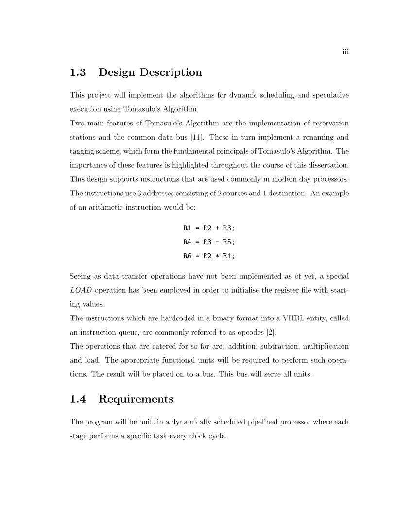
1.3 Design Description
This project will implement the algorithms for dynamic scheduling and speculative
execution using Tomasulo’s Algorithm.
Two main features of Tomasulo’s Algorithm are the implementation of reservation
stations and the common data bus [11]. These in turn implement a renaming and
tagging scheme, which form the fundamental principals of Tomasulo’s Algorithm. The
importance of these features is highlighted throughout the course of this dissertation.
This design supports instructions that are used commonly in modern day processors.
The instructions use 3 addresses consisting of 2 sources and 1 destination. An example
of an arithmetic instruction would be:
R1 = R2 + R3;
R4 = R3 - R5;
R6 = R2 * R1;
Seeing as data transfer operations have not been implemented as of yet, a special
LOAD operation has been employed in order to initialise the register file with start-
ing values.
The instructions which are hardcoded in a binary format into a VHDL entity, called
an instruction queue, are commonly referred to as opcodes [2].
The operations that are catered for so far are: addition, subtraction, multiplication
and load. The appropriate functional units will be required to perform such opera-
tions. The result will be placed on to a bus. This bus will serve all units.
1.4 Requirements
The program will be built in a dynamically scheduled pipelined processor where each
stage performs a specific task every clock cycle.

iv
The main aim of building such a model is to produce a sequence of correct results
from instructions every clock cycle by avoiding structural, data and control hazards.
Hazards exist from dependencies and the solution to this will be to implement a
method proposed by Robert Tomasulo in 1967.
Multiple functional units will be employed along with a register renaming policy [1].
Functional units use reservation stations which will buffer instructions before they
are executed.
The functional units employed so far are: an adder, performing both addition and
subtraction, and a multiplier performing multiplication.
A single bus, called a common data bus, will also be implemented.
The function and importance of all of these will be emphasised throughout.

Chapter 2
Background Research
2.1 IBM Systems 360
The Systems 360 computer family is where Tomasulo’s Algorithm originated [1]. The
following chapter gives an overview of how, why and when Tomasulo’s Algorithm was
developed.
2.1.1 Computer Family
The IBM1 System/360 is a family of computer systems, developed in the 1960’s, where
the chief architect was the well known Gene Amdahl [17]. Prior to the announcement
of this family, computers were custom made and designed independently. This de-
velopment of computers indicated that a new revelation was underway and would
change the computer industry forever.
Initially only 6 models were announced: 30, 40, 50, 60, 62, and 70, whereas in actual
fact 14 models were produced: 20, 22, 25, 30, 40, 44, 50, 65, 67, 75, 85, 91, 95 and
the 195 [17].
Despite the models’ individual differences, the System 360 family employed the same
user-instruction set. The larger machines dealt with complex instructions through
1International Business Machines
v

vi
hardware whilst the smaller ones dealt with them in micro-code, where such an in-
struction as multiplication would be completed by repeated addition. And as we know
today, this was an extremely inefficient way to execute a multiplication instruction
[10]. (It was also rumoured that the smaller 360 machines performed addition by
repeated increments! (i.e. x + 5 → add a 1 bit five times!) [13]
The System 360 employed a variety of operating systems [14]:
(i) DOS/360
(ii) OS/360
(iii) CP-67 (later VM/370)
(iv) MTS
(v) CRJE
(vi) TSO
(vii) Amdahl’s UTS
The OS/360 proved to be the most popular.
2.1.2 Motivation behind Tomasulo’s Algorithm
The 360 computer family had a very limited number of registers that initially con-
sisted of only four double precision floating-point registers. Consequently compiler
scheduling was not particularly effective. On top of this, even the more optimal 360
designs took considerable time to access memory and compute long floating point
equations. Due to the number of constraining factors, this prompted programmers to
develop a solution, so as to attain maximum efficiency [12]. The ultimate solution to
the problems comes in the form of Tomasulo’s Algorithm. See section: 4.2
2.1.3 Model 91
Tomasulo’s Algorithm was first designed for the IBM system 360 Model 91(360/91),
which produced the initial protocol in 1964, but didn’t employ Tomasulo’s Algorithm

vii
until 1967. The Model 91 of the 360 family had the most advanced internal architec-
ture of all System 360 computers and of any other computer of its time [14].
The reason behind this was that the algorithm, designed by Robert Tomasulo, sup-
ported dynamic scheduling and instruction level parallelism.
The Model 91 was specifically designed to perform high-speed data processing, di-
rectly intended for scientific purposes. Such intentions included space exploration,
theoretical astronomy, subatomic physics and global weather forecasting [14].
The model had three specific advanced features, giving it the capabilities to perform
speeds never before achieved.
These included:
1. Sophisticated circuits, which had the ability to switch in billionths of seconds
2. High density circuit packaging techniques
3. High degrees of concurrency i.e. parallel operators
These three factors were superior in the day and provided the Model 91 with the
resources to perform up 16.6 million additions per second. Also said to compute more
than one thousand problems a day, requiring approximately 200 billion calculations,
and subsequently providing 50 times the arithmetic capacity of previous models [10].
The Central Processing Unit (CPU) also played a part in this increased processing
power, as it contained five independent execution units allowing the system to process
many instructions simultaneously.
The five units were:
(i) Processor Storage
(ii) Storage Bus Control
(iii) Instruction Processor
(iv) Fixed Point Processor

viii
(v) Floating Point Processor.
These units had the ability to perform several functions at the same time and, addi-
tionally, all five could operate in parallel. Such designs were an incredible revelation
in 1967, despite being very familiar to Computer Scientists today, and are now com-
monly known as pipelining. See section: 3.1
The Model 91 had a CPU cycle time2 of 60 nanoseconds and a Memory cycle time of
780 nanoseconds [10].
2.2 NASA and the Model 91
The Model 91 was the first computer to be described as a supercomputer 3. Initially,
it was designed for the North American Missile Defence System. Interestingly, the
S/360 was IBM’s most expensive project, and equally its most risky. IBM bet the
whole company on the 5 billion dollar project [14] (equating to 30 billion dollars in
today’s terms). Obviously they’ve never looked back.
The most expensive computer project of the 1960’s was the moon exploration Apollo
Program, with the IBM’s S/360 bid coming in second place! However, the Apollo
Program actually relied quite extensively on the System 360, and in particular on
the Model 91, which was installed for this program at NASA’s Goddard Space Flight
Center, Greenbelt, Md.
The Model 91, operated with 2,097,152 bytes of main memory, interleaved 16 ways
and could accommodate 6,291,496 bytes of main storage. It could also store more
than 300 million characters in 2 drum and direct access storage units [10]. It was the
fastest and most powerful computer. See figure: 2.1
2cycle time: the time that elapses from the beginning to the end of a process3The class of fastest and most powerful computers available

ix
Figure 2.1: The Model 91 at NASA’s Goddard Space Flight Center [14]

Chapter 3
Advanced Pipelining Features
3.1 Pipelines
Pipelining is one of the most useful methods in increasing processor speed and com-
poses the basic structure of most modern general purpose computers. The pipeline
design breaks down a sequence of processes into a number of sub processes. These
sub processes can be identified as a stage. Each stage has a specific task, performing
a particular function and producing an immediate result.
When coding a pipeline in hardware, latches (or registers) are employed to enable the
flow of instructions. At the end of each clock cycle, each stage sends its results into
the latches at the end of the stage. The latches hold these results for use of the stage
coming immediately after the latch [7].
In a classic pipeline there are five stages:
1. IF (Instruction Fetch)
• fetches the instruction pointed to by the Program Counter (PC)
• increments the PC
2. ID (Instruction Decode)
• decodes the instruction (opcode)
x

xi
3. OF (Operand Fetch)
• fetches the required sources
4. EX (Execute)
• performs the operation
5. WB (Write Back)
• writes the results to the destination register
See figure: 3.1
Figure 3.1: A basic pipeline
In the pipeline above, instruction i begins in the first clock cycle, and fetches
its instruction.
In clock cycle 2, j begins, fetching its instruction, whilst i decodes its own instruc-
tion.
In clock cycle 3, k begins, fetching its instruction, whilst j decodes, and i fetches
its operands.
In clock cycle 4, i executes, whilst j fetches its operands and k decodes its instruc-
tion.

xii
In clock cycle 5, i has completed and writes the result, whilst j executes and k
fetches its operands.
In clock cycle 6, j writes it result whilst k executes.
And in clock cycle 7, k writes its result.
Pipelines imply an in-order-execution process, disallowing one instruction to bypass
another and making full use of the CPU. Therefore an out-of-order dynamic schedul-
ing algorithm is used, which will be explained in more detail.
The Tomasulo Algorithm, despite being modelled around the classic 5 stage pipeline,
employs only 3 stages:
1. Issue: get instructions from the instruction queue
2. Execute: perform operation on operands
3. Write Result: finish execution, i.e. write result
See detailed explanation in section: 4.2
3.2 Dependencies
Dependencies, which are simply scheduling constraints, are properties of programs.
i.e. if two instructions are data dependent, they cannot execute simultaneously.
A dependency results in a hazard.
3.2.1 True Data Dependencies
An instruction, i, is dependent on an instruction, j, when the following conditions
hold:
1. Instruction, i, writes to a destination that instruction, j, uses as a source.
2. Instruction, j, is data dependent on instruction, k, which is data dependent on
instruction i.

xiii
3.2.2 Name Dependencies
A name dependence occurs between two instructions using the same register or mem-
ory location, however no data flow exists between them. There are two different types
of name dependencies.
Anti-dependence: When instruction j writes to a register or memory location that
instruction i uses as a source.
i ADD R6, R5, R4
j SUB R5, R8, R11
Output-dependence: When instruction i and j write to the same register or
memory location, the ordering must be preserved to ensure the correct value is
in the register.
i ADD R7, R4, R3
j ADD R7, R2, R8
3.2.3 Control Dependencies
A control dependence determines the ordering of an instruction, with respect to a
branch instruction so that the instruction is executed in correct program order.
3.2.4 Resource Dependencies
An instruction is resource dependent on a previously issued instruction if it requires a
hardware resource which is still being used by a previously issued instruction. Toma-
sulo’s Algorithm is not overly concerned by this dependency.
There are two ways in which dependencies are checked:

xiv
• Statically by the compiler at compile time.
or
• Dynamically by the hardware at run time.
The compiler can sometimes overlook dependencies, as not all operations will have
addresses at compile time. Dynamically checking however should catch most depen-
dencies. One of the most common techniques of dynamic dependency checking is
Tomasulo’s Method.
3.3 Hazards
One of the major issues of pipelining is hazards. A hazard prevents a correct program
from functioning properly. Hazards are a result of a dependency.
There are three types of hazards:
3.3.1 Structural Hazards
Structural Hazards exist when two or more instructions try to use the same resource
at the same time. For example if a register file has only one read/write port, then a
pipeline wanting to perform 2 register writes in one clock cycle, is not able to.
A solution to this is to add more hardware i.e. use register files with multiple in-
put/output ports or, as in my design, implement multiple execution units.
3.3.2 Data Hazards
If an instruction requires the result of a previously issued instruction, but this previ-
ously issued instruction has not yet been completed, then a data hazard exists.
Data hazards can be eliminated by forwarding or bypassing. (Discussed in detail
below.)
There are three primary types of data hazards:

xv
• Read after Write Hazards (RAW)
i1 ADD R2, R2, R4 R2 = R2 + R4
i2 ADD R5, R2, R1 R5 = R2 + R1
Instruction, i2 can only read from R2 after instruction i1 has successfully writ-
ten to it, so as i2 obtains the most updated register value.
See the following diagrams:
Figure 3.2: i1 followed by i2 in a pipeline
Figure 3.3: Two stage stall must occur
i2 must wait until i1 has written back before it fetches its operands.

xvi
Figure 3.4: Solution to the two stage stall
• Write after Read Hazards (WAR)
i1 ADD R2, R3, R4 R2 = R3 + R4
i2 ADD R4, R5, R6 R4 = R5 + R6
Instruction i2 can only write to the register R4 after i1 has read from it.
• Write after Write Hazards (WAW)
i1 ADD R2, R3, R4 R2 = R3 + R4
i2 ADD R2, R5, R6 R2 = R5 + R6
Instruction i2 must write to register R2 after i1 has written to it, so as the
most up-to-date value is obtained.
3.3.3 Control hazards
When a branch is taken, the pipelines performance is seriously affected as it must
essentially drain and refill.
Time is needed to load the Program Counter (PC) with the target address when a
branch or a jump is taken. An instruction such as a branch causes a change in the
program flow.
The Branch instruction requires a new address to be loaded into the PC, which could

xvii
also have detrimental effects on all other instructions by invalidating them.
There are three branch types:
Unconditional: An unconditional branch will always alter the sequential flow of a
program. It will set the new target address in the PC.
Conditional: A condition must be satisfied for the branch to be taken. If it is
satisfied, then a new target address is sent in and the PC points to it. These
branches are the hardest to handle.
Loop: This type of branch causes the program to jump back to a particular point
in the program and execute it ‘n’ number of times.
IF ID OF EX WBIF ID OF
IF IDIF
IF ID OF EX WBIF ID OF EX WB
Table 3.1: Demonstrates the penalty caused by a branch
A solution to control hazards is to correctly predict the flow of the program by a
technique called Branch Prediction. There are two other solutions sometimes used to
solve these hazards: delayed branching and multiple prefetching.

xviii
Solution to hazards:
A general solution to eliminate hazards is to stall the pipeline until the hazard has
been resolved itself. However, we unquestionably want to avoid this, as it causes
degradation to the CPU’s throughput1.
Stalls due to the above three hazards increase the CPI2 for the pipeline:
It is necessary to minimize stalls to get maximum efficiency from the pipeline. To
do this, we determine which instructions can be performed in parallel without causing
any hazards.
3.4 Instruction Level Parallelism
The execution of multiple instructions, simultaneously, in a processor is called In-
struction Level Parallelism (ILP). ILP provides the basic fundamentals of modern
day processors [1]. It allows the overlap of individual machine operations.
With very few exceptions, all microprocessors today are out-of-order issue super-
scalar 3 processors. These processors follow a cycle of fetching, scheduling and issuing
of instructions. With each generation of Information Technology, we see increasingly
advanced features being added to exploit ILP.
But why this huge success for superscalar processors?
• They execute code without the need to recompile.
1Number of instructions completed in one clock cycle2Clock cycles per instruction3Hardware designs that support simultaneous processing of multiple instructions.

xix
• They can make use of runtime information to their advantage.
• They can exploit speculative techniques, such as data, value, address and de-
pendencies predictions.
Due to these characteristics, for the foreseeable future, superscalar processors will
dominate.
3.5 Dynamic Scheduling
Dynamic Scheduling is the execution of sequential programs out-of-order. It is a
hardware technique used to better exploit Instruction Level Parallelism. Dynamically
scheduled machines were termed superscalar computers in the 1980’s.
3.5.1 The Idea
Pipelines, as previously mentioned, execute instructions strictly in the same order as
they are inputted. Therefore, if one instruction stalls, all following instructions will
stall. Dynamic Scheduling allows instructions to bypass each other. They are issued
in-order in the first stage but executed out-of-order in the second stage by overtaking
one another if a leading instruction stalls.
3.5.2 Overcoming Data Hazards with Dynamic Scheduling
Dynamically Scheduled Algorithms are implemented in the hardware. They deter-
mine which instruction will be executed next. The order of execution is based on the
availability of the operands.
There have been various proposals for such schemes; - Thornton’s Scoreboarding
method and Tomasulo’s Algorithm are the most well known today.
Thornton’s technique is simple and centralised. It relies on a portion of hardware that
acts like a scoreboard. The scoreboard monitors the functional units and instructions

xx
waiting to be issued.
Unlike the sophisticated algorithm developed by Tomasulo, this technique does not
remove hazards, it only avoids them, by allowing highly inefficient stalls.

Chapter 4
Tomasulo’s Method
4.1 History of Tomasulo
Tomasulo’s Method is named after the computer architect, Robert Tomasulo, who
designed the floating point unit for the IBM 360/91 [9]. Tomasulo was an architect
for IBM. In 1967 he published a paper which proposed a method that resolved haz-
ards in the datapath of the processor. Prior to this, processors only had the ability
to avoid hazards as opposed to fully solving them.
Today, a very large number of microprocessors use Tomasulo’s Method to implement
out-of-order execution, including the full series of Pentium Processors.
In 1997, Tomasulo received the Eckert-Mauchly Award [16] for his outstanding con-
tributions to the field of computer and digital systems architecture. Specifically titled
“For the ingenious Tomasulo’s algorithm, which enabled out-of-order execution pro-
cessors to be implemented”. This is an award granted by the ACM1 and the IEEE2
Computer Society. It has been said that this was a very long awaited award, and
deserved well before the year it was presented, considering the phenomenal impact it
has had on today’s computer architecture.
1Association for Computing Machinery2Institute of Electrical and Electronics Engineers
xxi

xxii
4.2 Tomasulo’s Algorithm
In brief, Tomasulo’s Algorithm supports in-order issuing and out-of-order execution
of machine level code. The instructions are dispatched to the datapath in a particu-
lar sequence but leave the datapath in an entirely different order - the aim being to
execute the instructions according to dataflow as opposed to sequential order. The
question then is: How do we maintain this data consistency throughout the sequence
of instructions?
The method proposed by Tomasulo uses an intelligent renaming method and operand
tracking system, to resolve hazards and dependencies. This is implemented through
a sophisticated tagging scheme.
Tomasulo began with two functional units: an adder/subtractor and a multiplier/divider.
He recognized that the relationship between a current instruction and all incomplete
instructions must be distinguished so as to determine any existing dependencies. He
could then realize his main objective, which was to preserve essential precedences
while allowing the greatest possible overlap of independent operations [9].
Tomasulo states three requirements that must be maintained:
1. Recognize the existence of a dependency
2. Cause the correct sequencing of the dependent instructions
3. Distinguish between the given sequence.
Points number 1. and 2. must be maintained to preserve the integrity of the program,
while point 3. is required to meet the performance goal [9].
This original proposal was limited to 2-address instructions (1 source and 1 destina-
tion, R3 += R4). However it can be easily extended to handle 3-address instructions
(R2 + R5 = R7), as are used in most processors today. It also did not support inter-
rupts. However, a re-order buffer may be implemented to deal with these [15].

xxiii
Upon an instruction entering the datapath, it receives a tag. This tag will stay with
the instruction as it travels through from its initial stage of “issue” to its final stage
of “write back”.
These tags are determined by a hardware device called a Reservation Station(RS).
An RS stores an instruction until it has the values A and B that are required for
the instruction to execute. The instruction will sit in the reservation station whilst
it gathers the required values, using the information provided by the opcode.
There are a number of locations in an RS, so multiple instructions can be stored.
Each of these locations has a unique identity tag. It is this identity tag, that attaches
itself to all registers associated with the particular instruction. It enables the design
to maintain data consistency throughout the entire sequence execution.
To explain the algorithm as concisely as possible I have outlined the main functions
of the extra units needed to implement such a design. In the following section we will
work through a concrete example.
The tagging system enables the continuous tracking of operands which minimizes
RAW hazards, and the register renaming minimizes the number of WAW and RAW
hazards.
This method has two major advantages over previous schemes [1].
1. Distribution of hazard detection logic: achieved from the distributed reser-
vation stations and the common data bus
2. Elimination of stalls for WAW and WAR hazards: achieved by register
renaming and by the process of storing operands into the reservation stations.
As mentioned in Section 3.1, the Classic Pipeline executes in five stages, whereas
Tomasulo’s Algorithm implements only three stages:
1. Instruction Issue:
An instruction is sent from the instruction queue if, and only if, there is an

xxiv
empty space in the appropriate reservation station. If the operand values exist
in the register file, they are sent to the reservation station. If the operation is a
load or store, the value is issued if there is an available buffer. The registers are
renamed (or tagged in the case of Tomasulo’s Method) if required. If there is
no empty reservation station or buffer, then an unpreventable structural hazard
occurs.
2. Execute:
If operations have not arrived at the reservation station to complete an in-
struction, the common data bus is snooped3 for values. When a value becomes
available, it is placed in all units that require it. When the reservation sta-
tion has both operand values, the instruction is sent to the functional unit and
executed.
3. Write Result:
When the functional unit has executed the instruction, the result is written to
the common data bus and then to the reservation stations where required.
4.3 Constructs of Tomasulo’s Algorithm
4.3.1 Reservation Station
There is a reservation station (RS) for each of the functional units in the model.
Essentially a reservation station is a buffer. It stores an issued instruction awaiting
operands. It holds these instructions until the instruction has received the operand
values it requires for execution.
In my code the fields in the RS are as follows: A busy bit to indicate if a particular
slot in the RS is available for an instruction to be held. An op field to determine
what operation will be executed. Qa and Qb fields, which determine where the value
3continually monitor

xxv
A or value B will come from. Va and Vb fields, indicating the exact value of A or
B. And also a Tag Va and Tag Vb fields, which signify when the actual values of the
operands have been obtained. There is also a unique tag in the RS to identify the
various slots available. This unique tag is attached to the destination register in the
Register Status Table.
4.3.2 Register Status Table
The Register Status Table (RST) is a piece of hardware attached to the register file.
It is similar to a RS as it buffers information for the unit it is associated with.
Each register has an associated tag field in the RST. This 4 bit tag indicates which
RS the value will come from and also determines whether or not a register is waiting
for a more up-to-date value or whether it has an actual valid value. The tag indicates
which RS the value will come from.
As the functional unit’s RS’s are filling up with the required information they will
consult the RST to see if it is permissible or not to take the value in the desired
register. If it is, the value is placed in the V field; if it is not, the tag is placed in the
Q field.
4.3.3 Common Data Bus
The common data bus receives its inputs (values) from the functional units. Upon
receiving a result from a functional unit, the common data bus sends the result to all
units via their reservation stations (except the Load unit) and as a result speeds up
the execution by bypassing the architectural registers.

xxvi
4.4 Worked Example of Tomasulo’s Algorithm
To explain the the internal workings of Tomasulo’s Method, I will outline how the
two most important tables manage the instructions to be executed.
The tables will be shown step by step, from holding no information to managing
instructions at the RS’s full capacity.
Firstly we take a simple sequence of machine code:
ADD R2, R4, R0
SUB R3, R6, R2
ADD R5, R3, R2
instruction operation destination source 1 source 2
i1 ADD R2 R4 R0i2 SUB R3 R6 R2i3 ADD R5 R3 R2
Table 4.1: Sequence of 3 instructions
Instructions are dispatched from the instruction queue in-order. It is in the reser-
vation station where the order changes.
The first instruction ADD R2, R4, R0 (R2 = R4 + R0) is sent to the reservation
station.
There are two main stages in the management of an instruction. (For stage 1 of the
first instruction, see the associated table labelled step 1. For stage 2 of the first in-
struction see the associated table labelled step 2. For stage 1 of the second instruction,
see associated table labelled step 3. etc.)

xxvii
1. • Declare the first available RS location as busy. In this case Add 1 is
declared as busy.
• Set the destination register, R2, as busy by sending the RS name (unique
tag) to the RST.
In this example, the tag for the Add 1 location is sent to R2’s tag in the
RST. From this point in time, any instruction that requires to read from
this register, R2, will now only read the tag value. (When a tag value exists
in the RST, it signifies that the actual value currently held in the register
is no longer up-to-date, and it is waiting for an instruction to execute and
write the result back.)
• The type of operation, ADD, is also recorded by the RS (this informa-
tion will then be forwarded to the functional unit, when the instruction is
ready.)
See figure: 4.1.
Reservation Station and Register Status Table
Figure 4.1: Step 1: first instruction (registering instruction)

xxviii
2. Search for actual operand values. Source registers are identified by reading the
opcode.
• Source 1: Check the status of the register, R4, in the RST.
If the register’s tag is clear then the RS can read in the actual value held
in the register.
In this example, the status of R4 is checked; it is clear. Therefore the
actual value is placed in the Va field. The Tag Va field is also set to signify
that source 1 has been obtained.
• Source 2: Check the status of the register, R0, in the RST.
It too is clear. Therefore the actual value is placed in the Vb field. The
Tag Vb field is also set to signify that source 2 has been obtained.
See figure: 4.2.
Reservation Station and Register Status Table
Figure 4.2: Step 2: first instruction (searching for operand values)

xxix
The second instruction SUB R3, R6, R2 (R3 = R6 - R2) is sent to the reser-
vation station.
1. • The first RS location Add 1 is already occupied, so Add 2 is checked. It
is free and the instruction claims the location by declaring it as busy.
• Next, the destination register, R3, is set as busy by sending the RS name
(unique tag) to the RST. In this example, the tag for the Add 2 location is
sent to R3’s tag in the RST. From this point in time, any instruction that
requires to read from this register, R3, will now only read the tag value.
• The type of operation, SUB, is also recorded by the RS.
See figure: 4.3.
Reservation Station and Register Status Table
Figure 4.3: Step 3: second instruction (registering instruction)

xxx
2. Search for actual operand values.
• Source 1: Check the status of the register, R6, in the RST.
In this example, R6 is clear. Therefore the actual value is placed in the
Va field. The Tag Va field is also set to signify that source 1 has been
obtained.
• Source 2: Check the status of the register, R2, in the RST.
It, however, is not clear. Therefore the tag value associated with R2 is
placed in the Qb field. The RS will have to hold this instruction until this
tag has been cleared. The way in which this tag is cleared and the actual
value obtained will be described in detail further on.
See figure: 4.4.
Reservation Station and Register Status Table
Figure 4.4: Step 4: second instruction (searching for operand values)

xxxi
The third instruction ADD R5, R3, R2 (R5 = R3 - R2) is sent to the reservation
station.
1. • The first and second RS locations are already occupied, so Add 3 is
checked. It is free and so the instruction claims the location by declar-
ing it as busy.
• Next, the destination register, R5, is set as busy by sending the RS name
(unique tag - Add 3 ) to the RST.
• The type of operation, ADD, is also recorded by the RS.
See figure: 4.5.
Reservation Station and Register Status Table
Figure 4.5: Step 5: third instruction (registering instruction)

xxxii
2. Search for actual operand values.
• Source 1: Check the status of the register, R3, in the RST.
R3 is not clear. Therefore the tag in the RST is sent to the Qa field.
• Source 2: Check the status of the register, R2, in the RST.
It too is not clear. Therefore the tag value associated with R2 in the RST
is placed in the Qb field.
See figure: 4.6.
Reservation Station and Register Status Table
Figure 4.6: Step 6: third instruction (searching for operand values)
When all locations of an RS are occupied, a signal is sent to the instruction queue
to tell it not to dispatch any more instructions to that RS.
Once the RS has both values required for the instructions execution, the instruction
is sent to the functional unit and the RS location is freed up for another instruction
to enter.
When an instruction is sent to the functional unit, the unique tag of the RS is also
sent. The instruction is executed and the result (along with the tag) is placed on the

xxxiii
common data bus (CDB). This bus will serve all RS’s avoiding the need to store the
results in the register file first.
When a result and tag comes in from the CDB, the RS compares the bus’ tag with
all the tags held in the RS. If there is a match, the tag is cleared and the result is
placed in the V field.
Example continued...
The instruction in Add 1 has been dispatched from the RS, as it had both its actual
values. The instruction executes in the functional unit and is placed on the common
data bus. See figure: 4.7.
Reservation Station and Register Status Table
Figure 4.7: Step 7: Instruction dispatched
The common data bus then sends the result along with the tag to all the RS’s.
Tag ResultAdd 1 Regs[R2]
Table 4.2: Tag and Result from CDB

xxxiv
All the tags in the RS’s are checked to see if they match the tag from the CDB.
See figure: 4.8.
Reservation Station and Register Status Table
Figure 4.8: Step 8: Result comes from the CDB
When a match is found, the actual result is placed into the V fields in the RS and
the tag in the RST is cleared.
We can also see that the instruction in Add 2 is now ready to be dispatched, as both
its V fields have been filled, indicated by the Tag Va and Vb fields. See figure: 4.9.
Reservation Station and Register Status Table
Figure 4.9: Step 9: Result from the CDB is placed in the RS’s

xxxv
4.5 Summary
To sum up, the main points to note on Tomasulo’s Algorithm are:
• The reservation station provides hazard detection and execution control.
• Results are passed directly to functional units rather than through the registers.
• A common data bus allows all units waiting for an operand to be loaded simul-
taneously.

Chapter 5
Software and Hardware
5.1 Software - VHDL
The software I chose to design my project was VHDL (VHSIC1 Hardware Description
Language). VHDL is a standard HDL regulated by the IEEE. It is used to describe
the structure and behaviour of digital systems. A logic synthesis tool “Model Sim”
is used to simulate (execute) the design. It provides us with an interface in which
the values of the inputs and outputs of the design are displayed. The approach used
in the design of hardware is a bottom-up approach where the design is described at
primitive gate levels and built up from there to form ‘entities’. Many entities are
created and then connected in a top-level design. Once an entity is created it can be
synthesised and simulated to check for any errors. Once the code runs at a synthe-
sisable and simulated form, a ‘testbench’ is then created to verify the functionality of
the code.
A testbench was created for each of my entities to guarantee the accuracy of my
design. Testbench waveforms are very useful as we can verify the correctness of the
circuit without having to build the circuit and test on the chip.
Synthesis
Synthesis is a process of transformation where the algorithmic abstract design is
1Very High Speed Integrated Circuit
xxxvi

xxxvii
translated into a detailed structural model of gates and optimized at that level. [8]
Simulation
Simulation is a process where the coded design is analyzed under a set of conditions.
This is carried out by specifying the possible inputs and outputs into the design.
The simulation software “Model Sim” then executes the design under the conditions
and produces the outputs. These are manually checked from a testbench waveform
(examples are explained in detail in Section: 6.2) to see if the expected results have
been achieved. [8]
Both of these processes were of utmost importance in ensuring my project was func-
tioning as expected.
5.2 Hardware - FPGA
An FPGA (Field Programmable Gate Array)2 is a reprogrammable integrated circuit
board. The FPGA in which my design had to be fully compliant with was the FPGA
SPARTAN XC3 S1000.
2An Integrated Circuit board which can be programmed by downloading code on to it

Chapter 6
Code Design
6.1 Design Introduction
The design of my project was broken down into a number of steps:
Concept
The concept had to be established by analysis of all the available theory, outlined in
chapters 2 through 5.
Specifications
The specifications had to be verified. It was very important to ensure that my de-
sign be fully compliant with the FPGA SPARTAN XC3 S1000 hardware provided by
Trinity College.
Hardware designers, whilst coding through software are encouraged to “always think
hardware”, as code would be useless if it was not possible to implement it.
Therefore, even though downloading the project to the board was not the ‘aim’, the
design still had to be built to a fully synthesisable and simulated form so as it could
potentially be downloaded on to an FPGA.
Algorithm Design
This involved the design of the algorithms and the hardcode. This stage took up an
extensive amount of the design time.
xxxviii

xxxix
The hardcoded design has been done in two stages:
1. Design and code
2. Test and fix (redesign)
Whilst designing my code and writing the first draft of entities I came across many
problems, both in design and syntactical.
The design errors were mostly resolved by writing down examples and trying differ-
ent prototypes for different algorithms. I found many of these problems could also
be solved by spending time working through my original prototypes of the design in
my head or on paper. At that stage I could see where any glitches or errors occured,
and redesign and fix accordingly.
Many of the syntactical errors were resolved by searching books from the library, the
internet and talking to fellow VHDL’ers!
Design Entry
The top-level design then had to be entered into the FPGA design system. This is
done by means of a schematic (See figure: 6.1) and top level design code.
Synthesis
The next stage is logic synthesis, where the built in logic synthesis tool converts the
high level HDL into primitive blocks of logic.
Simulation
Following this is the simulation stage which checks for correct synthesis of the design
in accordance with the specifications. It was here that I was faced with many timing
issues. I had to repeat the Design Entry stage, fix errors, change constructs and
re-synthesis and re-simulate.
Testing
When I began the initial phase of testing I found that many sections of my code
didn’t work exactly as I expected them to.

xl
Many parts had to be redesigned or reordered, including many constructs so as opti-
mal timing was achieved and results produced in the desired clock cycle and so forth.
It is these problems where I feel I benefited most on the learning curve - and it is
these errors which I will discuss throughout this chapter.
6.2 Individual Entity Description
In this section I will explain each individual entity as they are designed in my code.
Below is the top-level schematic of the overall design. To fully understand and follow
the true internal workings of the individual entities it will be necessary to refer back
to this schematic. See figure: 6.1 Each entity will be described by listing the inputs
and outputs, and giving a detailed description of how the inputs travel through the
entity, eventually producing the outputs. The entity’s block form representation in
code will also be shown, along with an outline of the testing procedure. The testing
was carried out using Xilinx’s testbench waveform “Model Sim” Software.
Testbench waveforms of each entity are shown. A testbench will list all the inputs
to the entity and the modified outputs. Also an outline of any associated problems
and solutions will be detailed. Where problems and solutions are not listed it implies
there were no major difficulties worth noting.
All of the following entities (except the adder/subtractor1) are entirely my own work
and design. Only the required amount of bits specific to this project are used.
All the code of the following descriptions can be found on the attached CD.
6.2.1 Background Information
An instruction is entered in to the program, in the form of an opcode, operation
code. Essentially this is an instruction represented in binary format. The fields of the
opcode determine what is going to be computed;- what operation, on what operands,
1courtesy of Morris M. Mano [4]

xli
Figure 6.1: Top Level Schematic

xlii
and where the result will be stored.
The opcode is 15 bits long, see figure: 6.2
operation ⇒ 3 bits (0, 1, 2)
source 1 ⇒ 4 bits (7, 8, 9, 10)
source 2 ⇒ 4 bits (11, 12, 13, 14)
destination ⇒ 4 bits (3, 4, 5, 6)
Figure 6.2: Opcode
Slight problem - "0000000000000000": Technically, this could be an add opera-
tion R0 + R0 = R0;
Therefore, when the opcode leaves, a validity bit has been added, making it 16 bits
long. The validity bit will be 1 if the instruction is valid, and 0 if the instruction is
invalid.
Entities perform a check on the instruction to evaluate whether it is valid or not. If the
instruction is invalid, entities will simply disregard it and wait for a valid instruction
to arrive.

xliii
6.2.2 Instruction Queue
Inputs Outputs
clock opcode
reset
adder full
mult full
instruction
Detailed Design Description
This entity has two functions:
1. To take in instructions (and store if necessary).
2. To output an instruction per clock cycle.
The instruction queue is organized in to a stack format, following a FIFO2 queuing
structure. An incoming instruction is placed in the next lowest available position in
the stack. (e.g. if the last instruction was placed in position stack 4 - all positions
above it would be free and the next instruction would be placed in stack 5). There
is space for 16 instructions. See table: 6.1
2First In, First Out

xliv
stack 15
stack 14
stack 13
stack 12
stack 11
stack 10
stack 9
stack 8
stack 7
stack 6
stack 5
stack 4
stack 3
stack 2
stack 1
stack 0
Table 6.1: Stack format implemented in VHDL entity: Instruction Queue
To input an instruction:
There is a 4 bit count pos signal (an internal variable), which identifies the next
free space in the stack. It is essentially a program counter (PC). As instructions are
entered, this value increments.
A full flag is maintained throughout the entity. This flag is also declared as a signal.
It is set to zero when the instruction stack still has space for more instructions. When
an instruction is placed in position 15 of the stack, the full flag is set to 1, indicating
that there is no more space for instructions in the stack. If the user still continues to
enter instructions, they will simply be disregarded.
Each position of the stack is declared as a 16 bit signal. Initially, on reset, each of
these positions is set to ‘0’. i.e. "0000000000000000". The outputs and the signals
are initialized to zero.

xlv
The instructions that are catered for are:
operation binary code
Addition 000
Subtraction 001
Multiplication 010
Load 011
In time, other operations could also be added: e.g. STORE 100. Likewise, a num-
ber of logical operations or branch instructions could also be added.
The ADD operation, adds the contents of two registers and stores the result in a third.
The SUB operation subtracts the contents of one register from another register and
stores the result in a third, whilst the MULT operation multiplies two registers and
stores the result in the third. The LOAD is a special instruction, which at present is
used at the beginning of the program to initialise the contents of the register file.
Tomasulo’s algorithm can cater for any type of instruction, including branch instruc-
tions, logical instructions and data transfer instructions.
To output an instruction:
Instructions to be outputted will only come from stack 0. If stack 0’s validity bit
is equal to 1, then it can be assumed that this is a valid instruction that needs to be
outputted.
The three least significant bits of the instruction are evaluated to determine what
operation the instruction will perform. It can then be determined which reservation
station needs to be checked for availability.
There are two flags inputted to this entity indicating if the reservation stations have
a free position for an instruction or not.
mult full determines the state of the Multipliers reservation station, and adder full

xlvi
determines the state of the Adders reservation station. The instruction is dispatched
from the instruction queue if the following conditions hold:
1. There is a valid instruction in the stack.
2. The corresponding reservation station has an available space to accept the in-
struction.
When an instruction is dispatched, the count pos is decremented so as it points to
the previous position in the stack and the full flag is set to zero. Each time an
instruction is released stack15 is set to "0000000000000000", an invalid instruction.
All other stack positions must be moved down a space.
opcode <= stack0;
stack0 <= stack1;
stack1 <= stack2;
stack2 <= stack3;
Testing
At present this is the only entity that is not fully functioning. It correctly takes in
instructions and counts as expected. The problem lies in outputting the instructions,
and assigning each stack position to the stack position below.
Michael, my supervisor, has since advised me that I could use a pre-coded FIFO
entity from the internet but, due to time constraints, I could not implement this. It
does not however have an effect on the overall functionality of the top-level code and
I can still show the remaining entities working as required.
Problems and Solutions
1. Problem The user could enter an instruction where the operation is not one of
the arithmetic operations specified in this project.

xlvii
Solution Examine the operation bits and disregard any instructions that are not
applicable.
2. Problem As previously explained: Determining whether R0 + R0 = R0 is an
actual instruction or not, or whether it is set as this on reset.
Solution Add a validity bit to the opcode.
3. Problem Counting up as instructions were entered.
Solution Use different constructs and VHDL statements.
4. Problem Counting down when instructions are outputted.
Solution Unable to solve.

xlviii
6.2.3 Opcode to Functional Unit Selector
Inputs Outputsclock opcode out mult
reset opcode out add
opcode
Figure 6.3: opcode to fnUnit selector Entity
Detailed Design Description
This entity examines what operation is specified by the opcode.
On each clock cycle, a 16 bit value will go to both of the reservation stations, re-
gardless of the opcode’s destination. One opcode will be valid, and one will not. If
the operation is an addition or a subtraction then the opcode is sent to the adder
reservation station, whilst an invalid opcode is sent to the multiplier. If the opera-
tion is a multiplication, it is sent to the multiply reservation station whilst an invalid
opcode is sent to the adder RS. If the operation is a load, it will be sent directly to
the register file and ignored by the RS’s.
The reservation station that receives the invalid opcode will ignore it, whilst the one

xlix
receiving the valid opcode will perform accordingly.
On reset, the two outputs are set to "0000000000000000", i.e. both their validity
bits are set to zero making them invalid, so as internally the circuit will not recognize
nor perform on it.
Testing
In the testbench waveform below, a number of points of change are shown.
At point A, the opcode comes in. Its most significant bit is one, and therefore deemed
valid. Its three least significant bits are “000”: an add instruction and therefore
outputted via the opcode out add variable for the adder RS. The opcode out mult
variable remains as an invalid opcode, and will be ignored by the multiplier RS.
At points B and C an invalid opcode is entered, and therefore both output variables
are set as invalid instructions.
At point D another opcode comes in. Its most significant bit is one, and therefore
deemed valid. Its three least significant bits are “010”: a multiply instruction and
therefore outputted via the opcode out mult variable for the multiplier RS. The
opcode out add variable remains as an invalid opcode, and will be ignored by the
adder RS. See figure: 6.4
Figure 6.4: Testbench waveform - opcode to fnUnit selector

l
Problems and Solutions
1. Problem Outputting the correct instruction to ONE RS only.
Solution Output an invlaid opcode to the other RS.

li
6.2.4 Reservation Station
Inputs Outputsclock tag
reset R
opcode destination select
output A value A
output B value B
regStatus adder full
bus result mult full
bus result tag
Figure 6.5: reservation station Entity

lii
Detailed Design Description
The reservation stations were the most complicated entity in the design, providing
the bulk of the code.
It has three functions:
1. To gather instruction information in the RS by analyzing the opcode.
2. Snoop the common data bus for values that are required by waiting instructions.
3. Determine when instructions are ready to go to the functional units, and send
them.
The reservation station is divided up into blocks of storage. The information
provided by an instruction is inserted into a chosen block, and has control of it for
the entire duration of its time in the reservation station.
An RS can be represented in a table format, as seen in the worked example in figure
4.4
Below we can see the binary representation of the RS table described previously. See
figure: 6.6
Figure 6.6: Reservation Station
In the adder reservation station there are three of these blocks (Add RS1, Add RS2,
Add RS3), whilst in the multiplier there are only two of these blocks (Mult RS1,

liii
Mult RS2).
So as to avoid confusion, in this design description, the overall reservation station will
be referred to as the reservation station(RS), and the internal blocks will be referred
to as RSX, where X will donate position 1, 2 or 3 of the stations positions.
Each of these blocks is a 26 bit signal so far. (If other types of instructions and op-
erations were to be introduced then more bits may be added to cater for them.)
Each RSX is identified by a unique tag. Add RS1 = 0001, Add RS2 = 0010, and so
forth for all reservation stations in the program. Tag 0000 is not assigned to any RS
as this indicates no RS, (the importance of this will be discussed in detail later on).
Before any action occurs we must check the validity of the opcode, otherwise noth-
ing happens in the RS. If the opcode is valid, then the execution of the instruction
begins its complex journey.
Function 1.
The opcode is permitted to enter only when the RS has a free space for it.
Each RSX will be checked for availability by evaluating the RSX’s bust bit, which
in the code is its least significant bit (LSB). If the LSB = 0 then the opcode can
be entered here. If it is busy however, then the next RS is checked until an empty
location is found. Once an empty RSX has been chosen to manage the instruction,
it then sets the busy bit of the RSX to 1. All other instructions will now know this
location is busy.
There are two count values, adder full and mult full, which indicate the status
(i.e. its availability) of the corresponding reservation station. The appropriate count
is checked before an instruction is sent to an RS.
Next the opcode’s values are stored in the RSX:
The operation that the RSX will perform is stored in bits 7, 6 and 5. If the operation
is an add instruction, i.e. 000, then a 0 bit is sent to the adder-subtractor unit to
signify that it must perform an addition. If the operation is a subtraction, then it is

liv
sent a 1 bit. This bit is represented in the code as the output ‘R’.
destination select is an 8 bit value which identifies the register will store the result
of this instruction and also identifies which RSX will produce it. Bits 7 to 4 hold the
identity tag of the RSX, and bits 3 to 0 hold the binary value of the register where
the result is to be stored.
The RSX is then concerned with finding the correct operands specified by the in-
struction.
Firstly RSX deals with source one of the instruction. Source 1 is a binary value, rep-
resenting one of the eight registers. Using a case statement, we find which register
we are concerned with. See the code in figure: 6.7
Figure 6.7: Determining the register

lv
Once source 1 has been identified it must then be determined if there is an available
value residing in the register or if the register is waiting for another RSX to produce
its result.
This is determined by the register status table, which is inputted into the RS in binary
format.
If the register is valid, the value can be transferred directly to the Va (for source 1) or
Vb (for source 2) fields. These values will come directly from the register file. So as
the values arrive at the same time that the RSX is looking for the values, the opcode
is sent simultaneously to the register file and to the RS. On the next clock cycle, the
reservation station will receive the results it needs.
If, however, the register does not immediately have the value then it must send its
tag. This tag will indicate where its value is coming from and is stored in the Qa or
Qb fields.
Once the Va or Vb fields have been filled, their corresponding tags are also set. When
both of these flags have been set, it indicates that the instruction is ready to be sent
to the functional unit for computation and its RSX can now be cleared, ready for use
by another instruction.
Function 2.
The reservation station constantly snoops the common data bus looking for values
that it requires to complete an instruction. The common data bus (CDB) holds a
result and its corresponding tag computed by the functional unit. The tag on the
CDB will be compared with the six Q fields in the reservation station searching for
a match. Upon finding a match, the Q field will be cleared and inserted into the V
field.
Function 3.
Once both V flags are filled, the reservation station must dispatch the fulfilled instruc-
tion to the functional unit for execution. The value B is determined by the RSX’s

lvi
Vb field and value A is determined by the RSX’s Va field. A tag output is also sent
along with these values to indicate where the instruction has come from. Once the
instruction is dispatched from the RS then the RSX is reset to all 0’s so as a new
instruction can occupy this space. See the code in figure: 6.8
Figure 6.8: Outputting the completed instruction
Testing
Testing this entity was a laborious task, taking up a significant amount of the allocated
testing time. It was, however, to be expected as the RS is the fundamental basics of
Tomasulo’s Method. If instructions can travel through this entity correctly (which
they can as shown below) then the most complicated part of the project has been
completed successfully.

lvii
See figure: 6.9
At point A, reset is set low, and the inputs are taken in from various entities. The
user specifies the instruction (opcode) which is a load operation. The RS does not
perform on load operations and simply ignores it. As a result we see no change in
any of the outputs.
At point B, another load operation is specified - again it is ignored by the RS, and no
change is seen in the outputs. The outputs remain at their initialised values specified
on reset.
Figure 6.9: (a) Testbench Waveform - RS
The following testbench is a continuation of the testbench in figure 6.9. At point
C another opcode is entered into the design. By examination of the most significant
bit the RS can tell it is valid and will execute it.
By further examination of the bits it can be seen that it is an add instruction “000”,
where the result will be stored in R2 “0010”, and the two sources are R6 “0110” and
R0 “0000”.
Immediately (on the first clock cycle after entry) the destination register is specified

lviii
as busy by sending a tag to the register 2 of the register status table. In this same
clock cycle, the full flag must be sent out to prevent an incoming instructions if the
RS is full.
On the second clock cycle after entry, the RS is able to output the values A and B.
Value A has been obtained directly from the register file “0011”, as the RST input
did not hold a flag for R6. However, by examination of the four least significant bits
of the registerStatus input it can be seen that R0 does hold a flag - but at the same
time a flag is sent from the common data bus. These two flags match and therefore
Value B can be set to the result of the common data bus “0111”.
I have included three temp values of the three locations in the RS so as the changes
can be seen as the RS obtains the required values.
At point D the next opcode comes in. By examination of the bits we can see the
instruction is: R1 = R2 - R7
Again on the first clock cycle (point E), the outputs destination select and
adder full are outputted correctly. destination select is set to “00100001” where
the tag of the Add RS2 will be sent to R1 tag of the RST, specifying that it is not
yet holding an actual valid value. At point F the values A and B are again obtained
and outputted. Value A can be seen to be obtained from output a which comes from
the register file, whereas value B can be seen to be obtained from bus result. See
figure: 6.10

lix
Figure 6.10: (b) Testbench Waveform - RS
We can see in this continuation of the following RS testbench that the correct
results are produced successfully on every clock cycle. See figure: 6.11
Figure 6.11: (c) Testbench Waveform - RS
Problems and Solutions
1. Problem Initially I had implemented a count signal. When an opcode occupied
an RSX space, the count was incremented. When the instruction had finished with

lx
the RSX and dispatched to the functional unit, the count was decremented. When
the count reached 3 in the adder’s reservation station, then the output adder full
was set to one. This count however did not seem to implement correctly.
Solution I then removed it, and by evaluating the RSX’s busy bits determined the
full values. If all RSX’s were busy then the adder full displayed a 1 value, indicating
the entire reservation station was tied up. This works perfectly.
2. Problem There were also numerous timing problems. In this screen-shot of the
testbench waveform, we see that the result isn’t actually computed until the third
clock cycle. See figure: 6.12
Figure 6.12: Testbench Waveform - timing error
The Problem here is that the destination select value is incorrect. At point
A the destination register specified by the opcode is “0010” or R2. It is the first in-
struction entered in to the entity and should therefore occupy the first location in the
RS, namely Add RS1, resulting in the 4 most significant bits of destination select
being “0001” and the 4 least significant bits being “0010” representing R2. In this
testbench waveform we can see this result is achieved a clock cycle too late (point

lxi
B) causing a fatal error.
Solution It is of vital importance that this value is sent out exactly when an instruc-
tion is assigned to an RSX so as data consistency is maintained. This is to prevent
any other incoming reading from the destination register and picking up the old value
and not the new tag.
As we can see in the testbenches above this problem has been rectified. The design
did not have to be changed but many of the VHDL statements did.
3. Problem
Case choice must be a locally static expression.
Failed to simulate annotated test bench
Solution: I then used if statements. I searched the web and there seems to be the
general consensus that there is an error with VHDL in this particular case. See code
below: 6.13 and 6.14.

lxii
The following code..
Figure 6.13: Caused error
..had to be changed to..

lxiii
Figure 6.14: Fixed error
.

lxiv
6.2.5 Adder-Subtractor
Inputs Outputsinput A result
input B tag out
R C4
tag
Figure 6.15: adder subtractor Entity
Detailed Design Description
There are a variety of techniques used to design the functions addition, subtraction
and multiplication. The skeleton of this particular adder-subtractor came courtesy of
Mano. [4] However, it had to be modified slightly to employ the tag in and out.
It employs three entities:- an exclusive-or, and a series full adder and half adders.
The mechanics of these are not important to this project.
It has a simple but effective functionality. It receives a value A and a value B from
the reservation station, along with a tag value, which is always associated with the

lxv
operations and attached to the result when it departs from the adder-subtractor.
The adder-subtractor must also be told if it is to perform addition or subtraction.
This bit is sent from the reservation station after careful examination of the opcode.
The result of the computation and the tag out are outputted to the common data
bus.
When the operation is an add, the R bit is set to ‘0’; when it is a subtraction however,
it is set to ‘1’.
Testing
It is a fully successful working entity, which has been tested and proves that it correctly
adds and subtracts two values. See figure: 6.16
When R = 0 input a + input b = result
When R = 1 input a - input b = result
Ex 1. On clock cycle 1: Ex 2. On clock cycle 2:R = 0 R = 1
input a = 3 input a = 5
input b = 0 input b = 2
result = 3 result = 3
3 + 0 = 3 3 + 0 = 3
Figure 6.16: Testbench Waveform - Adder/Subtractor

lxvi
6.2.6 Common Data Bus
Inputs Outputsadder tag data tag
adder result data IN
Figure 6.17: common data bus Entity
Detailed Design Description
The common data bus receives a result and an associated tag from the functional
unit. The common data bus then delivers this result to all the reservation stations.
The outputted result is called data IN, signifying that it is internal data, and the
tag is called data tag. So far the common data bus only deals with the result of the
adder.

lxvii
6.2.7 Register File
Inputs Outputsreset output A
clock output B
opcode
destination result
select data
data EX
data IN
Figure 6.18: register file Entity

lxviii
Detailed Design Description
A register is a group of flip flops and gates that effect their transition. The flip flops
hold the binary information and the gates control when and how the new information
is transferred into the registers.
When the opcode is read in, I am only concerned with the values determining sources
1 and 2, which the corresponding select lines are set to. These select lines chose the
appropriate register to output their values. As we never require more than 2 variables
A and B, we only have a pair of buses connected to the reservation stations.
Each register connects to the 2 multiplexers. The select lines feed into the multiplexer
and chose the specified register. The multiplexer then outputs the values of the
register via output A and output B.
destination result is read from the registerStatus table and determines the
register into which the result (data IN or data EX) should be written.
The select data is sent form the registerStatus table to indicate that internal
data is coming in. data IN represents internal data(select data is set = 1), whereas
data EX represents external data (specified by the user) (select data is set = 0).

lxix
6.2.8 Register Status Table
The mechanics of this entity are slightly different to the reservation stations of the
functional units, however, is still essentially an RS as it buffers information about its
associated unit.
Inputs Outputsclock select data
reset destination result
destination sel temp result
CDB tag compare temp reg status
CDB result
Figure 6.19: register status table Entity
Detailed Design Description
Inputs
1. Specify the destination of the instruction as being busy as soon as it enters the
RS. This is done by sending destination sel from the reservation station. The first

lxx
four bits represent the RSX it has come from, and the last four bits represent the
destination in which the result of this RSX must be stored.
2. The common data bus must also be monitored for results. The two inputs from
the CDB consist of a result (CDB result) and a tag (CDB tag compare). The tag will
be that of the RSX that was managing the instruction that produced the result.
The destination result is sent to the register file and is then used to determine
the register in which the value temp result will be stored.
Outputs The temp reg status is outputted to the reservation stations of the func-
tional unit so they can see the present state of the registers (i.e. determine if a register
is currently ready to give a value or not). A select data line is set to 1 to tell the
register file to load data from the register status table rather than loading external
data. In the register file, the select data will be set back to 0.
Problems and Solutions
The registerStatus table caused many errors.
1. Problem A case statement was used to compare the tag of the result from the
common data bus to all tags in the registerStatus table.
The error result I received was:
Case choice statement must be a locally static expression
Failed to simulate annotated testbench
see picture
Solution: I found that I could get an equally efficient performance by using if
statements to compare the tags to each of the four bits representing each register in
my register file.
2. Problem Initially I had inputted the opcode into the register status table. This
opcode was used to determine the destination register, and it would link up with the

lxxi
tag of the RSX being sent from the reservation station entity. On occasions, these
two values did not arrive together at the same time, and another opcode could be in
place before the tag arrived from the RSX.
Solution I sent the destination register and the tag concatenated from the reservation
station. This ensured the correct timing and as a result the correct inputs to the
registerStatus table.

Chapter 7
Review
7.1 Future Work
There is much scope for expanding this project and it would make for a good contin-
uation project.
Data Transfer Operations: As described previously, loading values into the regis-
ter file is possible. However, given more time, I would implement separate load and
store buffers. To do this, I would add another bus line from the instruction queue,
bringing the data transfer operations to their appropriate buffer via the address unit.
This, in effect, creates an extra queue: one being a memory instruction queue, the
other being a general instruction queue.
Logical Operations: An ALU (Arithmetic Logic Unit) could be implemented.
Branch Instructions: Much work would have to go into this area including building
a Branch Controller.
Optimisation: Finally the overall project could be fully optimised.
7.2 Personal Conclusion
When beginning this project, I had very little confidence in my programming abilities.
Due to this I felt it difficult to ask for help and guidance. On many occasions I got
lxxii

lxxiii
stuck on minor errors, and got bogged down trying to solve them. As a result, over
the first few weeks, I spent a lot of time on the less important aspects of the project.
The ideas and concepts are difficult to understand from reading the literature.
I wrote to many forums and computer science message boards and feel that many
students only had insight into text book material. I, however, have been provided
with a fantastic insight to the practical world of computer architecture, in particular
by taking on this final year project.
I feel that I have been hugely challenged by this project. It is a hard task to turn
theory into code and I feel that I have exceeded my own expectations as far as the
learning curve goes for an final year project.
When I looked back through my project diary, I realize how much I have learnt
throughout the year. Notes I have from the beginning show how little I knew when
I started off. However, despite the shaky start, as time went on I realised I was in
fact fully capable of a project of this nature. I now feel that I am fully competent in
all aspects of HDL programming and hope to find a job in this area on completion
of my degree. I have gained a vast amount of knowledge in this area and feel that I
now am a very confident HDL programmer.
7.3 Project Conclusion
To date, I have a fully simulated and synthesisable version of my design which in the-
ory could be downloaded on to an FPGA. However the top-level code needs tweaking
so as the sequence of results are produced correctly. At present the top-level code
only produces for the first instruction. Due to simulation, synthesis and extensive
testing of all internal entities, in particular the reservation station as I demonstrated
in my presentation, all required variables and values are working correctly within the
system. I am quite confident that the last few problems are due to timing difficul-
ties and could be fixed with a little more work, and the overall top-level code could

lxxiv
produce correct results for each instruction entered.

Bibliography
[1] Hennessey and Patterson, “Computer Architecture: A Quantitative Approach”,
Third Edition, “San Mateo, California: Morgan Kaufman Publishers”, 1990.
[2] Mano, M. Morris, “Logic and computer design fundamentals”, Third Edition,
“Englewood Cliffs, N.J.; London: Prentice Hall”, 2003.
[3] Zargham, Mehdi R., “Computer architecture: single and parallel systems”, “En-
glewood Cliffs, N.J.: Prentice Hall; London: Prentice Hall International (UK)”,
1996.
[4] Mano, M. Morris, “Computer engineering : hardware design”, “London: Pren-
tice Hall International”, 1988.
[5] Mano, M. Morris, “Computer system architecture”, Third Edition, “Englewood
Cliffs; London: Prentice Hall”, 1993
[6] W. RudinYalamanchili, Sudhakar, “Introductory VHDL: from simulation to
synthesis”, “Upper Saddle River, N.J.: Prentice Hall; London: Prentice Hall
International”, 2001.
[7] Floyd, Thomas L, “Instructor’s resource manual to accompany Digital funda-
mentals with VHDL”, “Upper Saddle River, N.J.; [Great Britain]: Prentice
Hall”, 2003.
lxxv

lxxvi
[8] J. B. Conway, “VHDL made easy!”, “Upper Saddle River, N.J.: Prentice Hall”,
1997.
[9] Wikipedia; http://www.wikipedia.org
[10] IBM Research Papers; www-03.ibm.com/ibm/history/reference/glossary 9.html
[11] Tomasulo, R.M., “An Efficient Algorithm for Exploiting Multiple Arithmetic
Units”, “IBM Journal 11, 34”, 1967.
[12] Amdahl, G.M., Blaauw G.A., Brooks, Jr. F.P., “Architecture of the IBMSys-
tem/360”, “IBM Journal 8, 2”, 1964.
[13] BeagleEars.com www.beagle-ears.com/lars/engineer/comphist/ibm360.htm#intro
[14] Columbia University http://www.columbia.edu/acis/history/36091.html
[15] Kent State University, Computer Science Department
http://www.cs.kent.edu/ batcher/CS675101/c3.html
[16] Eckert Mauchly Awards http://www.computer.org/awards/Eckert-
Mauchly%20Award.pdf
[17] IBM www.ibm.com