Study on optical Yagi-Uda antennas utilizing …...博 士 論 文 (Doctoral Thesis) Study on...
115
博 士 論 文 (Doctoral Thesis) Study on Optical Yagi-Uda Antennas Utilizing Localized Surface Plasmon Resonance of Metal Nanoparticles 金属ナノ粒子の局在表面プラズモン共鳴 を用いた光八木宇田アンテナの研究 小迫 照和 (Terukazu Kosako) 広島大学大学院先端物質科学研究科 Graduate School of Advanced Sciences of Matter Hiroshima University 2016 年 2 月 (February 2016)
Transcript of Study on optical Yagi-Uda antennas utilizing …...博 士 論 文 (Doctoral Thesis) Study on...
博 士 論 文 (Doctoral Thesis)
Study on Optical Yagi-Uda Antennas
Utilizing Localized Surface Plasmon
Resonance of Metal Nanoparticles
金属ナノ粒子の局在表面プラズモン共鳴
を用いた光八木宇田アンテナの研究
小迫 照和
(Terukazu Kosako)
広島大学大学院先端物質科学研究科
Graduate School of Advanced Sciences of Matter
Hiroshima University
2016年 2月
(February 2016)

目 次
(Table of Contents)
1.主論文(Main Thesis)
Study on Optical Yagi-Uda Antennas Utilizing
Localized Surface Plasmon Resonance of Metal Nanoparticles
(金属ナノ粒子の局在表面プラズモン共鳴を用いた光八木宇田アンテナ
の研究)
Terukazu Kosako(小迫 照和)
2.公表論文(Published papers)
(1) Design parameters for a nano-optical Yagi-Uda antenna.
Holger F Hofmann, Terukazu Kosako and Yutaka Kadoya.
New Journal of Physics, 9, 217, 1-12 (2007).
(2) Directional control of light by a nano-optical Yagi-Uda antenna.
Terukazu Kosako, Yutaka Kadoya and Holger F. Hofmann.
Nature Photonics, 4, 312-315 (2010).

主 論 文
(Main Thesis)

Acknowledgments
I performed this work when I was in the doctor’s course at the Graduate School
of Advanced Sciences of Matter, Hiroshima University, Japan.
I am extreamely grateful to Professor Yutaka Kadoya for providing me an
opportunity to study as a doctor course student and for giving me fruitful guidance and
timely encouragement to complete this research. I am sincerely grateful to Associate
professor Holger F. Hofmann as well for giving me strong support in my investigation
of theoretical models and the analysis of the experimental results. I am also deeply
grateful to Assistant professor Jiro Kitagawa (currently Associate professor at Fukuoka
Institute of Technology, Japan) for giving me kind pieces of advice and helping me to
maintain the experimental equipments. I am also deeply grateful to Mr. Hiroshi
Taniguchi (A technical staff in HU Technical Center at the time of this research) for
helping me to develop the measurement set up.
I was not able to accomplish this work without numerous kinds of support from
professors and researchers mentioned above.
I was financially supported by the USHIO Foundation during my master’s
course. The scholarship enabled me to make my endeavors to study at the doctor’s
cource. I am sincerely grateful to Professor Takayuki Takahagi for recommending me to
apply the scholarship.
Finally, I would like to express my gratitude to my family for their strong
support.

Table of contents
1. INTRODUCTION ...................................................................................................... 1
1.1. BACKGROUND: NANO-OPTICS AND PLASMONICS .................................................. 1
1. 1. 1. Propagating surface plasmon ..................................................................... 3
1. 1. 2. Localized surface plasmon (LSP) .............................................................. 5
1.2. OPTICAL ANTENNAS ............................................................................................... 9
1.3. PURPOSE OF THIS WORK ....................................................................................... 11
1.4. STRUCTURE OF THIS THESIS ................................................................................ 13
2. LOCALIZED SURFACE PLASMON RESONANCE IN METAL
NANOPARTICLES ...................................................................................................... 14
2.1. OPTICAL RESPONSE OF A SINGLE NANOPARTICLE ............................................... 14
2.1.1. Mie theory .................................................................................................... 14
2.1.2. Quasi static approximation ........................................................................ 16
2.1.3. Ellipsoidal metal particle ............................................................................ 18
2.1.4. Expression for the response of a point dipole including radiation
damping .................................................................................................................. 20
2.2. COUPLED DIPOLE MODEL FOR ONE-DIMENSIONAL NANOPARTICLE ARRAYS ... 24
2.3. DIELECTRIC CONSTANT OF GOLD ........................................................................ 26
3. RESONANCE IN NANOPARTICLE ARRAY ...................................................... 27
3.1. DIPOLE MODEL PREDICTION ............................................................................... 27
3.2. EXPERIMENTAL RESULTS ..................................................................................... 30
4. DESIGN OF NANO OPTICAL YAGI-UDA ANTENNA ..................................... 33
4.1. BASICS OF YAGI-UDA ANTENNA DESIGN .............................................................. 33
4.1.1. Yagi-Uda antenna in radio frequency region ............................................ 33
4.1.2. Optical Yagi-Uda antenna........................................................................... 35
4.2. DESIGN OF OPTICAL YAGI-UDA ANTENNA ........................................................... 38
4.2.1. Coupled dipole model ................................................................................. 38
4.2.2. Two-element antenna .................................................................................. 40
4.2.3. Three-element antenna ............................................................................... 44
4.2.4. Five-element antenna .................................................................................. 47
4.2.5. Effect of material losses on the directivity ................................................ 51
4.3. SUMMARY ............................................................................................................ 53

5. NANO-OPTICAL YAGI-UDA ANTENNA: EXPERIMENT .............................. 55
5.1. NANO PATTERN FABRICATION ............................................................................. 55
5.2. DRIVING METHOD OF ANTENNA .......................................................................... 57
5.3. MEASUREMENT SET-UP ........................................................................................ 59
5.3.1. Evaluation of resonant wavelength ............................................................ 59
5.3.2. Measurement of radiation pattern ............................................................. 59
5.4. DEMONSTRATION OF OPTICAL YAGI-UDA ANTENNA .......................................... 62
5.4.1. Antenna design & layout ............................................................................ 62
5.4.2. Resonant wavelength of each element ....................................................... 63
5.4.3. Directionality ............................................................................................... 66
5.4.4. Discussions ................................................................................................... 71
5.5. WORKING WAVELENGTH DEPENDENCE ............................................................... 77
5.5.1. Antenna design & layout ............................................................................ 77
5.5.2. Resonant wavelength of each element ....................................................... 78
5.5.3. Directionality ............................................................................................... 81
5.6. SUMMARY ............................................................................................................ 84
6. CONCLUSION ......................................................................................................... 86
REFERENCES ............................................................................................................. 89
APPENDIX I MATHEMATICA PROGRAM CODES ............................................ 96
APPENDIX II BI-LAYER RESIST PROCESS AND LIFT-OFF PROCESS ....... 105
APPENDIX III SAMPLE LAYOUT ........................................................................ 106
1
1. Introduction
1.1. Background: nano-optics and plasmonics
Since 2000s, nano-optics (or nanophotonics) has become an active research area for
understanding and applying optical phenomena on the scale near or beyond the
diffraction limit of light [1-3]. Nano-optics is encouraged by the rapid progress of
nanoscience and nanotechnology in the past a few decades, as well as motivated by the
need for new technology in the field of nanofabrication, information devices,
microscopy, and sensors. The plasmon, induced by coupling optical field with free
electrons in metallic structures, is widely utilized for realizing the required functions.
The significance of plasmonics can be recognized through outlining the historical
development of nano-optics and the contribution of plasmonics in that field.
Since the invention of optical microscopes in 17th century [1, 4], scientists had
advanced the spatial resolution. The optical theories developed in the 18th and 19th
centuries had encouraged the advancement. However, it was eventually recognized that
the diffraction limit of light restricts the resolution [5, 6]. In order to overcome the
limitation, for instance, far-field radiation is modified in the confocal microscopy [7, 8]
that has become one of the indispensable tools to observe the luminescent markers
tagged to molecules in the field of biotechnology.
On the other hand, as other schemes, Synge first proposed a type of the near-field
optics in 1928 [9, 10]. Figure 1.1 shows his concept that uses a tiny particle as a light
source (probe), and raster-scans the sample in close distance from the particle. Thus the
spatial resolution does not depend on the wavelength of light but on the size of the
probe. Today, his idea is well verified in the development of SNOM/NSOM (scanning
near-field optical microscopy) [10-17]. The development is based on the techniques to
fabricate sub wavelength-sized probe, as well as on the invention of scanning tunneling
microscopy in 1982 [18] that enables the distance to be regulated between the probe and
the sample with high accuracy. In order to ensure the effective coupling between the
probe and the sample surface, plasmonics is introduced. Success in the near-field optical
microscopy makes it possible for the plasmonics to be one of the core technologies in
the field of nano-optics.
Figure 1.2 describes the two fundamental modes of plasmon. They are roughly
classified by the propagation characteristics; propagating surface plasmon polariton
(SPP) which occurrs at the metal dielectric interface, and localized surface plasmon
(LSP) excited in metal nanostructure (e.g. nanoparticle). In the case of SPP, because of

2
the ohmic losses in the metal, the propagation length, at which the field decays to 1/e, is
limited to several tens of micrometers in optical regime. In the dielectric (air) side, the
optical field decays on the scale comparable to the wavelength of light. On the other
hand, the optical field of LSP in metal nanoparticle is confined in the vicinity of metal
surface in the range comparable to the particle size. Thus with the particle of the size
smaller than the wavelength of light, the optical field can be confined in the region
much smaller than the diffraction limit. The fundamental physics of SPP and LSP have
widely been investigated, and a wide range of applications has been demonstrated in the
last decades. In the following, some applications of SPPs and LSPs are reviewed.
(a) (b)
Fig. 1.1: Comparison of (a) conventional and (b) near-field optical microscopy [10]. (a) The
diffraction limits the resolution Δx to be about a half wavelength of light. Objective lens is
positioned in the far field. (b) The probe size d decides the resolution. The probe is positioned in
the near field of the sample.
(a) (b)
Fig. 1.2: Schematic view of electromagnetic distributions of two fundamental plasmon modes.
(a) Surface plasmon polariton (SPP) at the dielectric (air) metal interface. The electric field in
the dielectric (air) is confined in the range comparable to the wavelength λ of light. (b)
Localized surface plasmon (LSP) in a metallic sphere. The electric field is confined in the range
comparable to the radius r of the metallic sphere [1, 2].
Metal
Air
(Dielectric) Ez
~ 0.5λ z
z
Air
Metal
x
+ - + + - - + - + + - -
x
-
+ + +
- -
x
Er
Surface
Metal Air (Dielectric)
r
θmax
Objective
lens
Sample
R >> λ
Image-plane
Δx ~ λ/2
R << λ
d << λ
Sample Probe
Image-plane
Δx << λ
3
1. 1. 1. Propagating surface plasmon
The SPPs was at first recognized in the study of electron energy loss spectroscopy of
a thin metallic film. Apart from the bulk plasmon (longitudinal electron oscillations
within the bulk), Ritchie theoretically predicted an additional loss induced on the
metallic surface in 1957 [19]. Subsequently, Powell and Swan performed a
substantiative experiment with magnesium and aluminum in 1960 [20].
Figure 1.3 shows the dispersion of SPPs and the light lines. Excitation of SPPs (blue
solid line) is possible only if the wavenumber of light increases beyond the limit (light
line) in free-space. Therefore, phase-matching procedure is necessary to excite SPPs.
The methods that utilize an attenuated total internal reflection were independently
proposed by Otto [21] and Kretchmann [22] in 1968. Figure 1.4 illustrates their
configuration. Because of its simple procedure, Kretchmann’s configuration is
commonly used. In the configuration, thin metal film is deposited on the prism surface.
The evanescent wave, shown as red-solid line in Fig.1.3 (a), is induced by the incident
light at the metal/prism interface. Since its dispersion lies between the (air) light line
and the prism light line, the evanescent wave can excite the SPPs at the metal/air
interface. Note that the metal film should be thin enough for the evanescent wave to be
able to reach the metal-air interface. The theoretical model predicts that thin metal film
of a few ten nanometers is enough to obtain SPPs [1]. It is also known that the field
confinement normal to the surface becomes weaker for longer propagating length. This
trade-off should be considered in the waveguide application. It should be mentioned that
Takahara et al. [23] proposed a further confinement of the light field of SPP by
one-dimensional optical waveguides.
Otto and Kretchmann’s studies led to the development of an important application of
SPP. The high sensitivity of SPP excitation condition to the variation of surrounding
medium is applicable for sensors [24]. The variation is observed as the shift of resonant
spectrum of SPPs. In 1980s, for instance, gas sensing [25] and bio-sensing applications
[26] were demonstrated. Optical fiber based SPP sensors were also proposed to meet the
need for compact device and remote sensing in the field-use [27, 28].
In the bio-sensing (chemical) applications, the surface of metal film is usually
functionalized to react with the material that cannot bind directly to the bare metallic
surface. Figure 1.5 shows the functionalization by self-assembled monolayer (SAM)
film [29-35]. Since the thickness of SAM layer is typically a few nanometers, detection
of the local dielectric change on nanoscale is promising. For example, in-situ
measurement of protein binding was demonstrated [29, 30]. The other applications

4
include biotechnology [32], medical diagnostics [34], food safety [35], etc.
(a) (b)
Fig. 1.3: (a) The dispersion relation of SPP and light lines for the case of three-layer system
(air/metal/prism) [21, 22]. Light line is described by frequency ω, vaccum light speed c, and
wavenumber k as ω = ck. (1) light propagating in air, (2) light line, (3) evanescent wave at
metal/prism interface, (4) light line in prism (refractive index n >1), and (5) SPP at the metal/air
interface. (b) Configuration considered for (a).
(a) (b)
Fig. 1.4: Excitation of SPPs. (a) Otto configuration [21]. The metal and the prism is minutely
separated. SPPs is excited at the metal/air interface by the evanescent wave occured at air/prism
interface. (b) Kretchmann’s configuration [22]. Thin metal film is deposited on the prism
surface. The evanescent wave generates the SPPs at the metal/air interface.
Fig. 1.5: Self-assembled monolayer (SAM) enables SPP or LSPR based sensors to detect the
chemical reaction. Analytes bind only to a SAM having adhesive terminal.
Incident
Incident
metal
air
prism
SPPs
Evanescent wave
Reflection
Reflection
SPPs air metal
Evanescent wave
prism
Incident Reflection
Analyte (virus, antigen, DNA, etc.)
Adhesive
SAM (Length ~nm)
S S S
Metal Sulfer
Nonadhesive
Air
Metal
Prism kmed
k
ksp
kmed, x (= nk sinθ)
kevanescent
θ
θ0 kx
(2) ω = ck (vaccum, light line)
(5) SPPs (metal/air interface)
(4) ω = ck/n (prism light line)
(1) ω = ckx/sinθ0
(3) ω = ckx/(n sinθ)
(evanescent wave, θc≦θ≦90°)
Wavevenumber k, kx
Fre
quen
cy ω
5
1. 1. 2. Localized surface plasmon (LSP)
The excitation of LSP needs no phase-matching technique that is necessary for the
case of SPPs. Incident light to a metallic nanoparticle generates a collective oscillation
of free electrons in the nanoparticle, namely the excitation of LSP. In 1908, G. Mie
established an exact solution, so-called “Mie theory”, describing the scattering and the
absorption of light by a sphere [36]. This response can be approximated by an
oscillating dipole, which is called quasi-static approximation [37], provided that the
particle size is sufficiently smaller than the wavelength. With this approximation, the
electromagnetic field at a distance r from the dipole is described by the linear equation
of the terms 1/r3, 1/r
2, and 1/r [4]. The term of 1/r
3 corresponds to the optical near field.
The LSP induces resonant enhancement of the optical near field, called localized
surface plasmon resonance (LSPR), provided that the frequency dependent dielectric
constant of a metal εmetal (ω) and the surrounding medium εmed satisfy the relation
Re[εmetal (ωres)] = -2εmed. Here, ωres is the resonant angular frequency. The resonant
condition is ωres = ωp/ [37] for a nanoparticle of Drude metal of (bulk) plasma
frequency ωp located in air. Since the plasma frequencies of noble metals are around the
optical frequency region [38], nano-sized metals exhibit different colors from those of
the bulk. Surprisingly, this phenomenon had already been used in ancient times for
staining glass. Here, for example, consider the glass staining by gold nanoparticles.
Figure 1.6 plots the calculation results based on a quasi-static dipole model, described in
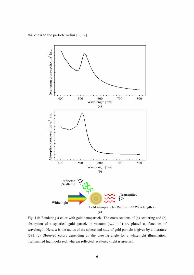
chapter 2, for scattering and absorption cross-sections of a spherical gold particle in
vacuum (εmed = 1). The maximum scattering and absorption exists around 530 nm. Note
that the LSPR wavelength does not depend on the radius of the sphere within the dipole
approximation. The absorption spectrum indicates that the transmission of white light is
red-colored, meanwhile the scattering spectrum shows that the reflection will be
greenish. The ancient Roman Lycurgus cup (4th century A.D.) [39-41] containing gold
nanoparticles is a well-known example that the transmitted light exhibits red color,
meanwhile the reflected light shows green color.
On the other hand, since nanoparticle size is small enough, its shape affects the
restoring force to the electrons, which decide the resonance condition of LSPR. Indeed,
the larger aspect ratio (= major/minor axis) of nanoparticle weakens the restoring force,
which results in the lower frequency of the resonant condition [37].
Internal configuration of a nanoparticle also modifies the LSPR. For example, a
core/shell nanoparticle, a dielectric nanoparticle coated with a thin metal layer, was
proposed. The arbitrary control of the LSPR is realized by adjusting the ratio of shell
6
thickness to the particle radius [3, 37].
(c)
Fig. 1.6: Rendering a color with gold nanoparticle. The cross-sections of (a) scattering and (b)
absorption of a spherical gold particle in vacuum (εmed = 1) are plotted as functions of
wavelength. Here, a is the radius of the sphere and εmetal of gold particle is given by a literature
[38]. (c) Observed colors depending on the viewing angle for a white-light illumination.
Transmitted light looks red, whereas reflected (scattered) light is greenish.
Transmitted
Reflected (Scattered)
White light
Gold nanoparticle (Radius r << Wavelength λ)
Wavelength [nm]
(a)
Wavelength [nm]
(b)
Sca
tter
ing
cro
ss-s
ecti
on
/a6
[a.
u.]
A
bso
rpti
on c
ross
-sec
tion /
a3 [
a.u.]

7
The significance of LSP in the field of nano-optics was recognized by the discovery
of surface-enhanced Raman scattering (SERS) observed on a roughened metal surface
in 1974 [42, 43]. Since Raman scattering [44] is an extremely weak effect, its
cross-section is typically 14-15 orders of magnitude smaller than that of the
fluorescence of dye molecules. However, the scattering as efficient as fluorescence was
reported under the condition that the molecules are located in enhanced electric fields of
LSP of a pair of metal particles, called hot-spots [45-47].
In a similar way, an acute metal probe positioned in the vicinity of the metal surface
can enhance the Raman scattering. This procedure is called tip-enhanced Raman
scattering (TERS) [14, 48-52]. Since only the near-field of the probe radiates the TERS
signals, imaging of TERS distribution is possible by raster-scanning of the probe.
Similar to the case of SPPs, LSP can be applied to the sensors. Since the resonance
condition of LSPR changes if the surrounding medium varies, the nanoparticles of noble
metals exhibiting LSPR in optical regime are proposed for sensing application [31-33,
53-59]. The LSPR-based sensor detects the surrounding medium only in the region of
confined field that is comparable to the size of nanoparticle. Using the functionalization
of the particle surface with a SAM layer, described in Fig. 1.5, the detection of chemical
bindings is enabled [31-33, 57].
On the other hand, the LSP of metal nanoparticles enables the fluorescence
enhancement by a factor of 10-1000 with respect to the measurement without metallic
structures [33]. In the field of medical diagnostics and biotechnology, for example, such
an enhancement is important since it enables an efficient detection of single molecule
[58], DNA hybridization [59], immunostaining [54], etc.
Since phase-matching technique is not necessary for exciting LSPR, just putting
nanoparticles at an end face of optical fiber can construct an optical sensor [60-62].
Such sensors have potential use in in-situ observation. For example, K. Mitsui et al. [62]
demonstrated an in-situ affinity measurement with high resolution of adsorption amount
10-12
g/mm2.
The other application of LSPR is an efficient solar-cells [63-66]. The Si-based solar
cells have a trade-off relation between the absorption layer thickness and the energy
conversion efficiency. The efficiency of thin-film cells is low compared to that of the
wafer-based cells. The electromagnetic enhancement effect of LSPR has been proposed
as one of the solutions to enhance the efficiency.
As described above, adjusting its shape, size, and surrounding medium can modify
the LSPR of a single metal nanoparticle. On the other hand, for the case of aggregated
nanoparticles, such modification also occurs by the mutual electromagnetic interactions

8
between the particles [67-72]. Figure 1.7 shows the schematic view of the interactions
for the two different cases of polarizations. The oscillating electrons in each particle are
either weakened or enhanced by the charge distribution of neighboring particles, which
will shift the spectral position of the plasmon resonance from that of the isolated
particle. The modulation will affect the operation of LSPR-based sensors, since they
observe the spectral shift of the LSPR. They usually consist of many particles to
enhance the detection signal. In this regard, the more sensitive detection than in the case
of random placement is promising by an adequate placement of nanoparticles for
obtaining desired spectral position and strength of the LSPR [69-72].
(a) (b)
Fig. 1.7: Schematic view of near-field electromagnetic coupling between neighboring particles
for the case of the polarization (a) perpendicular and (b) parallel to the array [3].
Inter-particle coupling is also utilized for an optical waveguide with the dimensions
below the diffraction limit of light [73-77]. In the case of linear array of nanoparticle,
the electromagnetic field is confined in almost one-dimension, and the propagation
length is estimated to be longer than micrometer distance [77]. Other applications
include random laser [78, 79], sub-wavelength imaging [80-82], and integrated optics
[76, 83-85].
Recentry, nanoparticls were proposed to be used as the elements to realize artificial
material called metamaterial that does not exist in nature. For example, in 2000, Pendry
proposed an application for negative-index materials, which can be used for perfect lens
of which the imaging resolution is not restricted by the wavelength [86-90].
Metamaterials utilize resonantly excited structures composed of the elements of which
the size is smaller than the operating wavelength. For example, a negative index about
-0.3 was demonstrated at the wavelength of 1.5 μm by an array of metallic nanorods
(width, 220 nm; length, 780 nm) [91].
9
1.2. Optical antennas
During the early years of the invention of near-field optical microscopy, the unique
perspective was recognized that there are similarities between the near-field probe and
radio frequency (RF) antennas designed to efficiently couple the far field radiation to
the feed element [10, 11, 92, 93]. Therefore, the antenna design concepts have been
tried to apply to the realization of a device that efficiently converts free-propagating
optical radiation to nanoscale emitter, and vice versa [94]. This conceptual antenna is
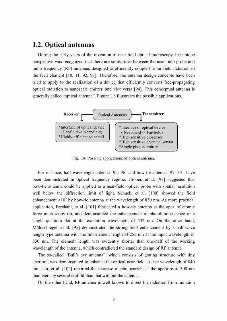
generally called “optical antenna”. Figure 1.8 illustrates the possible applications.
Fig. 1.8: Possible applications of optical antenna.
For instance, half wavelength antenna [95, 96] and bow-tie antenna [97-101] have
been demonstrated in optical frequency regime. Grober, et al. [97] suggested that
bow-tie antenna could be applied to a near-field optical probe with spatial resolution
well below the diffraction limit of light. Schuck, et al. [100] showed the field
enhancement >103 by bow-tie antenna at the wavelength of 830 nm. As more practical
application, Farahani, et al. [101] fabricated a bow-tie antenna at the apex of atomic
force microscopy tip, and demonstrated the enhancement of photoluminescence of a
single quantum dot at the excitation wavelength of 532 nm. On the other hand,
Mühlschlegel, et al. [95] demonstrated the strong field enhancement by a half-wave
length type antenna with the full element length of 255 nm at the input wavelength of
830 nm. The element length was evidently shorter than one-half of the working
wavelength of the antenna, which contradicted the standard design of RF antenna.
The so-called “Bull’s eye antenna”, which consists of grating structure with tiny
aperture, was demonstrated to enhance the optical near field. At the wavelength of 840
nm, Ishi, et al. [102] reported the increase of photocurrent at the aperture of 300 nm
diameters by several tenfold than that without the antenna.
On the other hand, RF antenna is well known to direct the radiation from radiation
*Interface of optical device
( Far-field -> Near-field)
*Highly-efficient solar cell
*Interface of optical device
( Near-field -> Far-field)
*High sensitive biosensor
*High sensitive chemical sensor
*Single photon emitter
Receiver Transmitter Optical Antennas
10
source. Usually, the directivity is expressed by the half-power beamwidth (HPBW)
defined as the angle between the half power points of the main emission lobe. Smaller
HPBW corresponds to the more concentrated radiation. Usually, an infinitesimally small
dipole antenna can represent the nanoscale optical emitter, and their HPBW is estimated
to be 90 degrees, indicating, for example, that a detector measures only a fraction of the
radiation [92]. Consequently, the exposure time is long to observe the weak fluorescent
signal of a single molecule. Intuitively, however, directing the fluorescent radiation to
the detector will be possible by procedure similar to the RF antena, which will
contribute to the efficient detection of living cells in the studies of DNA, and protein
molecules [45, 58, 103-112]. The efficient antibody test with a few samples will lead to
a shorter inspection time, and to the decrease of a burden on patients. The faster
detection also contributes to warding off the spread of disease.
Application of optical antennas to the optical information processing on nanoscale
was also proposed. Owing to the ability of speedier calculation without heat generation
that occurs in metal wire used in CPU, the application is attracting attention [113-117].
For example, a single nanoscale emitter for quantum computing, interface devices
between near field and propagating light, wireless optical communication between
antenna elements by developing a face-to-face connection, and optical data storage for
both writing and reading the data, etc. are expected [92].
Encouraged by these attractive applications, rapid progress has been made in the
realization of directional control of light with optical antennas. For instance, in 2007,
Taminiau, et al. [118, 119] demonstrated the directional control of light (λ = 514 nm) by
λ/4 antenna at the apex of the probe of SNOM/NSOM. The antenna design showed a
qualitative similarity to that of the RF antennas, but the element length was reduced
than in the case of the RF antenna. The effect of plasmon causes the difference, which is
similar to the result of the half-wave length type antenna described above [95].
Obvious fact that the plasmon effect in the antenna elements should be considered in
the realization of optical antennas suggests that the adoption of antenna theory to optical
frequencies is not straightforward. However, as seen above, applying the concept of RF
antenna to the optical wave will contribute to the realization of novel nanoscale optical
devices.

11
1.3. Purpose of this work
According to the RF antenna technology, directivity of a dipole antenna can be
increased by an appropriate arrangement of dipoles that interact with the radiation
source. The RF Yagi-Uda antenna is known to achieve the high directivity by a linear
array of properly tuned antenna elements. Figure 1.9 shows a typical geometry. The
antenna is driven only by a feed element, and the radiation from the feed drives the
other passive elements. Due to its simple structure and design, RF Yagi-Uda antennas
have been used worldwide for home TV, radio communication, and radar, etc [120,
121].
Fig. 1.9: Typical geometry of a five-element RF Yagi-Uda antenna.
What has inspired this work is the idea that the concept of the RF Yagi-Uda antennas
might be applied to the optical antennas. According to the scaling law, the element size
and its spacing would be around a fraction of the wavelength. This indicates the use of
metal nanoparticles as the antenna elements. Undoubtedly, LSPR should be considered
in the design, and precise arrangement of nanoparticles on nanoscale is necessary. This
implies the difficulty of design, fabrication, and directivity measurement.
However, there are attractive applications that make the effort worth challenging.
Since the Yagi-Uda antenna is driven only through the feed, it is very advantageous for
the directional control of single nano emitters. For example, it will contribute to the
efficient detection of fluorescent molecule by putting the molecule at the feed position.
Additionally, if the reciprocity of RF antenna is applicable, wireless communication
between two optical Yagi-Uda antennas arranged face-to-face is expected.
The purpose of this work is the clarification of the design and the realization of
directional control of light by an optical Yagi-Uda antenna [122, 123] consisting of
metal nanoparticles. Around the same time of this work, J. Li, et al. [124, 125] has
independently proposed the design of optical Yagi-Uda antenna but with different
elements. They considered core-shell nanoparticles, which are much more difficult to
realize than our proposal using simple metal nanoparticles, though the material loss
Reflector Feed Director
0.25λ ~0.3λ ~0.3λ ~0.3λ

12
could be a significant issue in our case. This work will validate that utilizing the
interaction between nanoparticles and adjusting carefully the shape of the nanoparticle
to the detuning are able to attain a similar function to that of RF Yagi-Uda antennas. The
result may encourage the development of further applications of RF technology to the
optical frequency regime.

13
1.4. Structure of this thesis
Figure 1.10 shows the contents of this thesis. Chapter 1 has described the background
and the purpose of this work. Chapter 2 will describe the dipole model of a single metal
nanoparticle, and the coupled dipole model that expresses the interaction between
nanoparticles. Based on this theoretical model, Chapter 3 will estimate how the
interparticle action affects the characteristics of the plasmon resonance. Chapter 4 will
explain in detail the design of a nano optical Yagi-Uda antenna by the coupled dipole
model. The effect of material losses on the performance of the antenna will be
considered. The behavior of reflector and director on the directivity of the antenna will
be clarified. On the basis of the antenna design obtained in Chapter 4, Chapter 5 will
describe the experimental validation that the nano optical Yagi-Uda antenna is able to
give high directivity to the optical emission in almost the same way as an RF Yagi-Uda
antenna does. The antenna is fabricated on a glass substrate by adopting the electron
beam lithography and lift-off process. The detail of the fabrication process will also be
described. The emission pattern from the optical antennas is measured by a set-up
specially designed for this work, based on the measurement systems for RF antennas
[126]. Chapter 6 will summarize the important findings and conclusions of this work.
Fig. 1.10: Contents of this thesis.
Chapter 1 Introduction
•Background & Purpose
Chapter 2 Theoretical Model
•Single particle (dipole model)
•Coupled dipole model
Chapter 3 Interparticle Interaction
•Example of coupled dipole model
Chapter 4 Design of Antenna
•Comparison between Radio frequency and Optical frequency
•Design method
Chapter 5 Experimental Result
•Measurement set-up
•Directivity
Chapter 6 Conclusion
•Research findings
•Further studies & Promising development

14
2. Localized surface plasmon resonance in metal
nanoparticles
In this work, a simple theory for describing the optical response of a nanoparticle
array to the external input is developed to design an optical Yagi-Uda antenna using the
interaction between nanoparticles [122]. In the development of the theory, both the
optical response of a single nanoparticle (Section 2.1) and that of a finite linear array of
nanoparticles (Section 2.2) are considered.
2.1. Optical response of a single nanoparticle
The theory of the optical response of nanoparticles small enough compared with the
wavelength of the incident light is summarized in this section [37].
2.1.1. Mie theory
Fig.2.1: Scattering of a spherical particle.
In 1908, G. Mie established an exact solution for the optical response of a spherical
nanoparticle [36]. Figure 2.1 shows the schematic illustration of scattering a plane wave
by a spherical particle of radius a, refractive index N1, surrounded by a uniform medium
of refractive index Nm. The orthonormal basis vectors êx, êy, êz are in the directions of
the positive X, Y, and Z axes in the Cartesian coordinate system. The Z-axis is the
propagation direction of the incident light which is assumed to be a plane x-polarized
wave written in spherical polar coordinates as Ei=E0eikrcosθ
êx. The scattering
φ
θ
Z
Y
X
êx
êy
êz
r
A
INCIDENT ( )

15
cross-section Csca of the spherical particle is given by Eq. (2.1).
(2.1)
Here, Wsca is the energy fraction passing through the surface A of an imaginary sphere
centered at the particle, Ii is the flux density of the incident light, k=2πNm/λ is the
wavenumber of the incident light of wavelength λ. The mode of scattering is designated
by n, for example, n=1, dipole; n=2, quadrupole. Under the condition that the
permeability of the particle is the same as that of the surrounding medium, scattering
coefficients an and bn are given by Eq. (2.2) and Eq. (2.3), respectively.
Here, Ψn and ξn are Riccati-Bessel functions expressed as Eq. (2.5) that is given by Eq.
(2.6) ~ Eq. (2.8). Equation (2.6) is the spherical Hankel function, Eq. (2.7) and Eq. (2.8)
are the spherical Bessel functions.

16
The resonance of the scattering occurs when the real part of the denominator of Eq.
(2.2) or Eq. (2.3) is zero, and the scattering cross-section Csca becomes resonantly large.
The resonance condition depends on the refractive index of the surrounding medium Nm,
the particle radius a, and the wavelength of the incident light λ.
2.1.2. Quasi static approximation
In this section, the quasi static approximation is considered which is valid under the
condition that the particle radius a is sufficiently smaller than the incident wavelength λ;
(a<<λ) [37]. When only the first few terms of an and bn in Eq. (2.2) and Eq. (2.3) are
considered, the approximate expression up to the term of x6 is obtained as follows.
When a<<λ, the size-parameter x defined in Eq. (2.4) is in the range of x<<1. With this
assumption, a1 can be further simplified as Eq. (2.10).
By substituting Eq. (2.10) and Eq. (2.4) in Eq. (2.1), the approximate expression of the
scattering cross-section Csca of the spherical particles is given as Eq. (2.11).
Here, ε1= is the dielectric constant of the particle, and εm=
is that of the
surrounding medium. The quantity (ε1-εm)/(ε1+2εm) suggests a connection to the
problem of a sphere embedded in a uniform static electric field [37].

17
The following is the consideration of a homogeneous, isotropic dielectric particle of
the radius a placed in the uniform static electric field E0 with the surrounding medium
uniform. Figure 2.2 shows the calculation model. The orthonormal basis vector êz is in
the direction of the positive Z, the center of the particle being set at Z=0. The dielectric
constant of the particle is ε1, and that of the surrounding medium is εm.
Fig. 2.2: Sphere in a uniform electrostatic field.
The polarizability α of the particle is given as Eq. (2.12), since the polarization induced
in the particle placed in an electrostatic field is equivalent to a dipole with the dipole
moment εmαE0 at Z=0.
Let us assume the same dipole in the case that the incident field is an x-polarized plane
wave E0exp(ikz-iωt). Then the dipole moment p=εmαE0exp(-iωt)êx is induced at Z=0
oscillating with the frequency of the incident field. The scattering cross-section Csca is
given as follows.
By substituting Eq. (2.12) into Eq. (2.13), Eq. (2.14) is obtained.
Equation (2.14) is the same as Eq. (2.11) that is obtained from the exact theory in the
limit of ka<<1. In general, the approximation Eq. (2.11) is called quasi static
approximation.
θ Z
r X
Y
E0
a

18
2.1.3. Ellipsoidal metal particle
Although the actual shape of the nanoparticles fabricated in this work is like a disk or
a rectangular block, a nanoparticle is assumed to be ellipsoid in the theoretical model,
because there is no approximation theory for irregularly shaped particles except for the
ellipsoid [37]. Figure 2.3 shows the ellipsoidal model. Semiminor axes a, b, and c
(a≧b≧c) are parallel to the x, y, and z axes defined in Cartesian coordinate system, in
which the center of ellipsoid is set as the center of the system. In order to obtain the
polarizability of ellipsoid with rotational symmetries, the traditional approach to the
solution of the Poisson equation has been adopted. For an ellipsoid of volume
V(=4πabc/3) and dielectric constant εp embedded in a homogeneous medium of
dielectric constant εm, the approximation of the polarizability αj in the field parallel to
one of its principal axes j (=x, y, z) is given by Eq. (2.15).
Fig. 2.3: Ellipsoidal model. The relations between the semiminor axes are a≧b≧c.
(2.15)
(2.16)
(2.17)
Here Nj is the shape-dependent depolarization factor. For example, to an electric field
parallel to the x-axis, Nx can be adjusted by varying the aspect ratio between the length a
along x and the perpendicular width b and c of the ellipsoid. The analytical expression
of Nj is already available for the sphere (a=b=c), the oblate spheroid (a=b>c), and the
prolate spheroid (a>b=c) [37, 127]. In this work, since the width and the thickness of
Z
X Y
a b
c

19
nanoparticles are designed to be equal, the shape of nanoparticles is assumed to be a
prolate spheroid for which the analytical expression of Nx, Ny, and Nz is given by Eq.
(2.18)~Eq. (2.20). The aspect ratio dependence of Nx is shown in Fig.2.4.
(2.18)
(2.19)
(2.20)
Fig. 2.4: Dependence of the shape-dependent depolarization factor Nx on the aspect ratio of a
prolate spheroid for which the analytical expression is given by Eq. (2.18)~Eq. (2.20) [37, 127].
The relations between the semiminor axes are a>b=c. Arrows next to each shape show the
direction of the incident electric field.
20
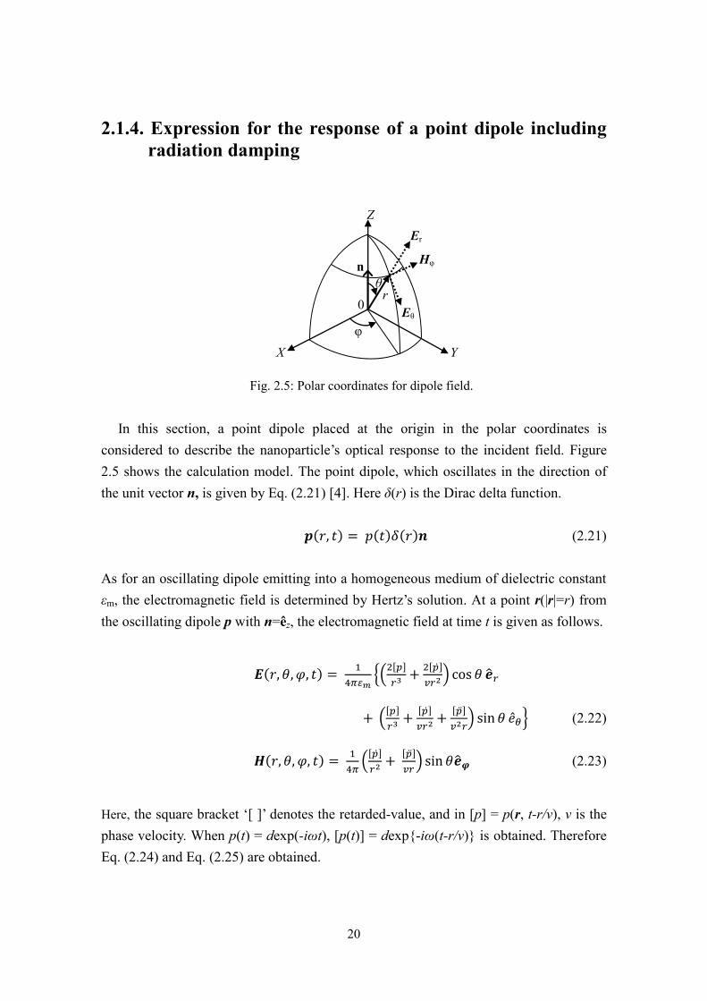
2.1.4. Expression for the response of a point dipole including
radiation damping
Fig. 2.5: Polar coordinates for dipole field.
In this section, a point dipole placed at the origin in the polar coordinates is
considered to describe the nanoparticle’s optical response to the incident field. Figure
2.5 shows the calculation model. The point dipole, which oscillates in the direction of
the unit vector n, is given by Eq. (2.21) [4]. Here δ(r) is the Dirac delta function.
(2.21)
As for an oscillating dipole emitting into a homogeneous medium of dielectric constant
εm, the electromagnetic field is determined by Hertz’s solution. At a point r(|r|=r) from
the oscillating dipole p with n=êz, the electromagnetic field at time t is given as follows.
(2.22)
(2.23)
Here, the square bracket ‘[ ]’ denotes the retarded-value, and in [p] = p(r, t-r/v), v is the
phase velocity. When p(t) = dexp(-iωt), [p(t)] = dexp{-iω(t-r/v)} is obtained. Therefore
Eq. (2.24) and Eq. (2.25) are obtained.
φ
θ
0
n
r
Eθ
Er
Hφ
X Y
Z
21
(2.24)
(2.25)
In the far-field, the terms proportional to 1/r in Eq. (2.22) and Eq. (2.23) are dominant.
Therefore, the pointing vector is given by Eq. (2.26) using Eq. (2.22) and Eq. (2.23).
(2.26)
The total radiation intensity per the unit time is given as Eq. (2.27) by integrating
Eq. (2.26) on the sphere with the radius r.
(2.27)
Therefore the energy lost by the dipole radiation in the time between t1 and t2 is given as
follows.
(2.28)
By choosing the time t1 and the time t2 so that the first term of the right-hand side of Eq.
(2.28) becomes zero, Eq. (2.29) is obtained.
(2.29)

22
On the othe hand, the energy loss is caused by the action of the electromagnetic
radiation, that is to say, the electric field Ereac generated by the electromagnetic radiation
of a dipole may affect the dipole itself. Then Wrad can be equated to the amount of the
work done by the electric field Ereac on the dipole,
(2.30)
By comparing Eq. (2.29) with Eq. (2.30), Eq. (2.31) is obtained.
(2.31)
Here λ(=2πv/ω) expresses the wavelength in the medium. In the linear response, the
dipole moment d induced by the incident field Ein is expressed as follows.
(2.32)
Here α is the polarizability. By rewriting Eq. (2.32), the expression for d including the
reaction field Ereac is obtained as follows.
(2.33)
Then Eq. (2.34) is obtained for the dipole in terms of the incident field Ein.
(2.34)
In the case when the polarizability is expressed in terms of the shape-dependent
depolarization factor, α is described as Eq. (2.15), or simply as Eq. (2.35).
(2.35)
23
By substituting Eq. (2.35) into Eq. (2.34), the dipole moment d induced by the incident
field Ein, including the effect of the radiation loss, is given as follows.
(2.36)
Equation (2.36) can be simplified, as follows.
(2.37)
(2.38)
(2.39)
(2.40)
Here, γ expresses the material loss and δ does the detuning relative to the radiation
loss. The parameter εr(=εp/εm) is the ratio of the complex dielectric constant of the
nanoparticle εp to the permittivity of the surrounding medium εm. The relation between
the detuning δ and the depolarization factor N is given by Eq. (2.39). Once the volume V
is fixed, δ can be determined by varying N, which can be estimated by the aspect ratio
of the nanoparticles as shown in Section 2.1.3. For example, a gold nanoparticle with
the resonant wavelength λ0=660 nm (δ=0) in vacuum, its width 2b, thickness 2c, and
length 2a are estimated to be 2b=2c=52.7 nm and 2a=125 nm, corresponding to 0.29λ
inside a glass (λ=435 nm, εm=2.3).
24
2.2. Coupled dipole model for one-dimensional
nanoparticle arrays
As shown in the previous sections, a small metal nanoparticle can be assumed to be a
dipole. Therefore, it is realistic to describe a finite linear array of nanoparticles by an
interacting dipole chain [122]. In order to consider the interactions in a nanoparticle
array, a coupled dipole model is developed on the basis of the dipole model described in
Section 2.1.4. By substituting X=(2πr)/λ, ω=vk, êθ =-êz, θ=π/2, and the wavenumber
k=2π/λ in the Eq. (2.24), the electric field EZ parallel to the dipole radiated from an
infinitesimally small oscillating dipole d at a distance of r perpendicular to the
orientation can be given as Eq. (2.41).
(2.41)
Here, λ is the emitting wavelength in a homogeneous medium of the dielectric constant
εm. By substituting Eq. (2.37) into Eq. (2.41), the following equations are obtained as
the description of the radiation from the oscillating dipole induced by the incident field
Ein.
(2.42)
(2.43)
(2.44)
Based on these equations, the responses of a finite linear array of dipoles are
considered. Figure 2.6 shows an example of the calculation model consisting of five
particles. The incident field Ein simultaneously drives the particles. Each nanoparticle
reradiates the field Erad. Each element is driven by the sum of the incident field and the
field radiated from other elements, as described by Eq. (2.45). They form a system of N
linear equations, where N is the number of nanoparticles [122].
25
Fig. 2.6: Example of a one-dimensional array consisting of five particles. Particles are aligned in
the X-direction, and the incident field Ein is polarized parallel to the Z-axis.
(2.45)
By solving the equations Eq. (2.45) for all the elements consistently, the ratio between
the radiation Erad,n and the incident field Ein is obtained.
X
(Center)
Erad,2 Erad, 3 Erad, 4 Erad,1 Erad, 5
X=0 Ein
θ
Z Y I(θ)

26
2.3. Dielectric constant of gold
In this work, gold is used as the antenna element. In the theory and the finite
difference time domain (FDTD) simulations, the dielectric constants of gold are
expressed as the sum of the Drude and the Lorentz functions, with the parameters
obtained by fitting the experimental values of the bulk gold reported by Johnson and
Christy [38]. The fitting equation is shown in Appendix I. The fitting of the real part
requires high accuracy, since it corresponds to the resonant wavelength as described in
Sec. 1.1.2.
Figure 2.7 shows the fitting result. The solid square marks (◆, ▲) and the open
square marks (◇, △) show the reported experimental values and the approximation,
respectively. In this work, the wavelength range of 400 nm ~ 900 nm is used.
Fig. 2.7: Fitting the measured dielectric constants of gold given by Johnson & Christy [38].
Solid (◆) and open (◇) marks show the reported values and fitting results for the real part,
respectively. Solid (▲) and open (△) marks show the reported values and the fitting results for
the imaginary part, respectively.
Wavelength [nm]
Die
lect
ric
const
ants
[a.
u.]

27
3. Resonance in nanoparticle array
The interaction between the metal nanoparticles, which can be described by the
coupled dipole model given in the previous chapter, is a key factor for operating the
optical Yagi-Uda antenna. The interaction-induced modification of localized surface
plasmon resonance (LSPR) in the metal nanoparticles is also expected to be useful for
sensitive plasmon sensors [67-72]. On the other hand, the effect makes it difficult to
evaluate the resonance wavelength of metal nano-patterns by a spectroscopic
measurement done with an array of the nano-patterns applied to enhance the detection
signal. Therefore, it is important to estimate how the interaction affects the
characteristics of the plasmon resonance. In this chapter, the dependence of the effect on
the distance between the particles arranged in a linear array is evaluated both
theoretically and experimentally.
3.1. Dipole model prediction
The calculation model is the same as that shown in Fig. 2.6. Under the condition that
the infinitesimal dipoles are equally spaced, the effect of interaction between particles
on the resonant wavelength (frequency) of the LSPR is considered. Each element is
driven by the incident field Ein=1 and the field radiated from the other elements.
According to Eq. (2.45), they form a system of N linear equations, where N is the
number of nanoparticles.
(3.1)
The Erad, n is obtained by the method described in Section 2.2. The emission intensity
detected at the Y-direction, as is determined in Fig. 2.6 is given as the superposition of
the radiation from all elements, as given by Eq. (3.2). Here θ is the angle between the
array axis and the emission direction in the X-Y plane determined in Fig. 2.6.
(3.2)
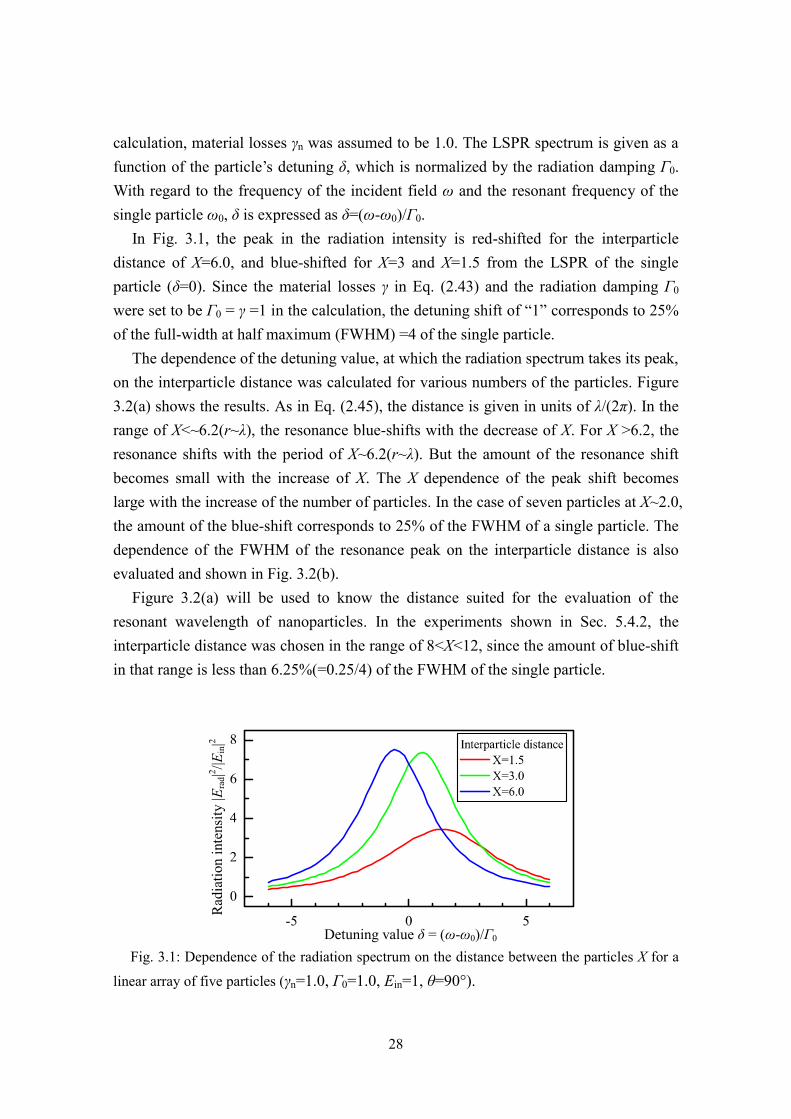
Figure 3.1 shows an example of the dependence of the radiation spectrum emitted in
the direction of θ=90° on the interparticle distance X in the case of five particles. In the
28
calculation, material losses γn was assumed to be 1.0. The LSPR spectrum is given as a
function of the particle’s detuning δ, which is normalized by the radiation damping Γ0.
With regard to the frequency of the incident field ω and the resonant frequency of the
single particle ω0, δ is expressed as δ=(ω-ω0)/Γ0.
In Fig. 3.1, the peak in the radiation intensity is red-shifted for the interparticle
distance of X=6.0, and blue-shifted for X=3 and X=1.5 from the LSPR of the single
particle (δ=0). Since the material losses γ in Eq. (2.43) and the radiation damping Γ0
were set to be Γ0 = γ =1 in the calculation, the detuning shift of “1” corresponds to 25%
of the full-width at half maximum (FWHM) =4 of the single particle.
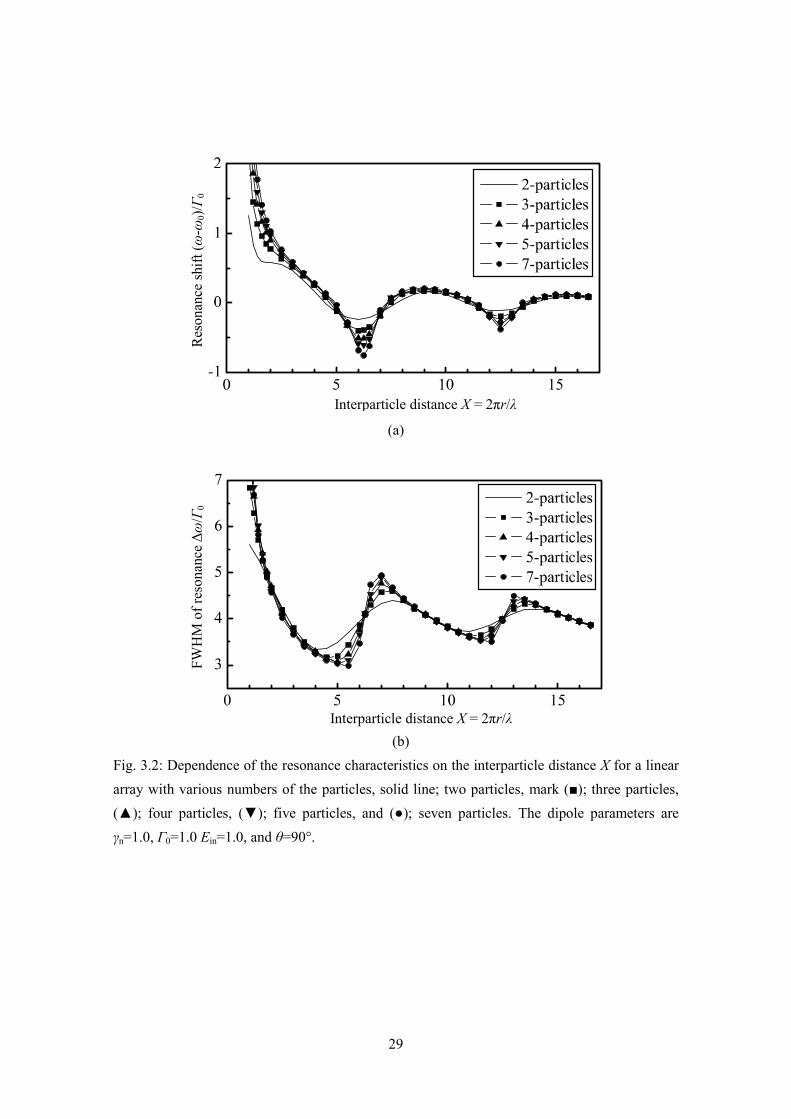
The dependence of the detuning value, at which the radiation spectrum takes its peak,
on the interparticle distance was calculated for various numbers of the particles. Figure
3.2(a) shows the results. As in Eq. (2.45), the distance is given in units of λ/(2π). In the
range of X<~6.2(r~λ), the resonance blue-shifts with the decrease of X. For X >6.2, the
resonance shifts with the period of X~6.2(r~λ). But the amount of the resonance shift
becomes small with the increase of X. The X dependence of the peak shift becomes
large with the increase of the number of particles. In the case of seven particles at X~2.0,
the amount of the blue-shift corresponds to 25% of the FWHM of a single particle. The
dependence of the FWHM of the resonance peak on the interparticle distance is also
evaluated and shown in Fig. 3.2(b).
Figure 3.2(a) will be used to know the distance suited for the evaluation of the
resonant wavelength of nanoparticles. In the experiments shown in Sec. 5.4.2, the
interparticle distance was chosen in the range of 8<X<12, since the amount of blue-shift
in that range is less than 6.25%(=0.25/4) of the FWHM of the single particle.
Fig. 3.1: Dependence of the radiation spectrum on the distance between the particles X for a
linear array of five particles (γn=1.0, Γ0=1.0, Ein=1, θ=90°).
Detuning value δ = (ω-ω0)/Γ0
Rad
iati
on
inte
nsi
ty |E
rad|2
/|E
in|2
29
(a)
(b)
Fig. 3.2: Dependence of the resonance characteristics on the interparticle distance X for a linear
array with various numbers of the particles, solid line; two particles, mark (■); three particles,
(▲); four particles, (▼); five particles, and (●); seven particles. The dipole parameters are
γn=1.0, Γ0=1.0 Ein=1.0, and θ=90°.
Interparticle distance X = 2πr/λ
Res
on
ance
shif
t (ω
-ω0)/
Γ0
Interparticle distance X = 2πr/λ
FW
HM
of
reso
nan
ce Δ
ω/Γ
0

30
dx
3.2. Experimental results
Transmission spectra of gold nanoparticle arrays were measured and compared with
the prediction shown in Section 3.1. Figure 3.3 shows the schematic diagram of the
samples. The arrays consisting of 50-nm-thick gold nanoparticles were fabricated
lithographically on a glass substrate with the area of 60 μm x 60 μm squares. The
incident field Ein was polarized parallel to the Y-direction as shown in Fig. 3.3 (a). The
distance dy was fixed to be 800 nm to suppress the interaction in the Y-direction while
dx was varied from 300 nm to 675 nm with a step of 25 nm. The nanoparticles were
embedded in a sputter-deposited SiOx (n~1.44) to suppress the effects of refractive
index discontinuity on the interaction between nanoparticles [123]. Figure 3.4 shows a
top-view SEM image and a top-view microscope image of the fabricated samples. The
size of the nanoparticles is measured to be ~50 nm in width and ~100 nm in length.
(a) (b)
Fig. 3.3: Schematic diagram of the sample. (a) Top view of the sample. The pitch in the
Y-direction was fixed to be dy=800 nm for all the samples. Incident field Ein was polarized
parallel to the Y-direction. (b) Side view of the sample. Gold nanoparticles were embedded in a
sputter-deposited 100-nm-thick SiOx (n~1.44).
(a) (b)
Fig. 3.4: (a) Top-view SEM image and (b) Top-view microscope image of the gold nanoparticle
array fabricated in an area of 60 μm × 60 μm with various dx(=300~675 nm).
10 μm
dy = 800nm Ein
X
Y
dx
Glass substrate
SiOx (n~1.44)
SiOx (n~1.44)
Au nanoparticle

31
Figure 3.5 shows the transmission spectra of various interparticle distance dx. The
resonant wavelength (dip wavelength of each spectrum) for dx=650 nm and dx=675 nm
were not estimated, because two peaks were observed in both cases. Figure 3.6 shows
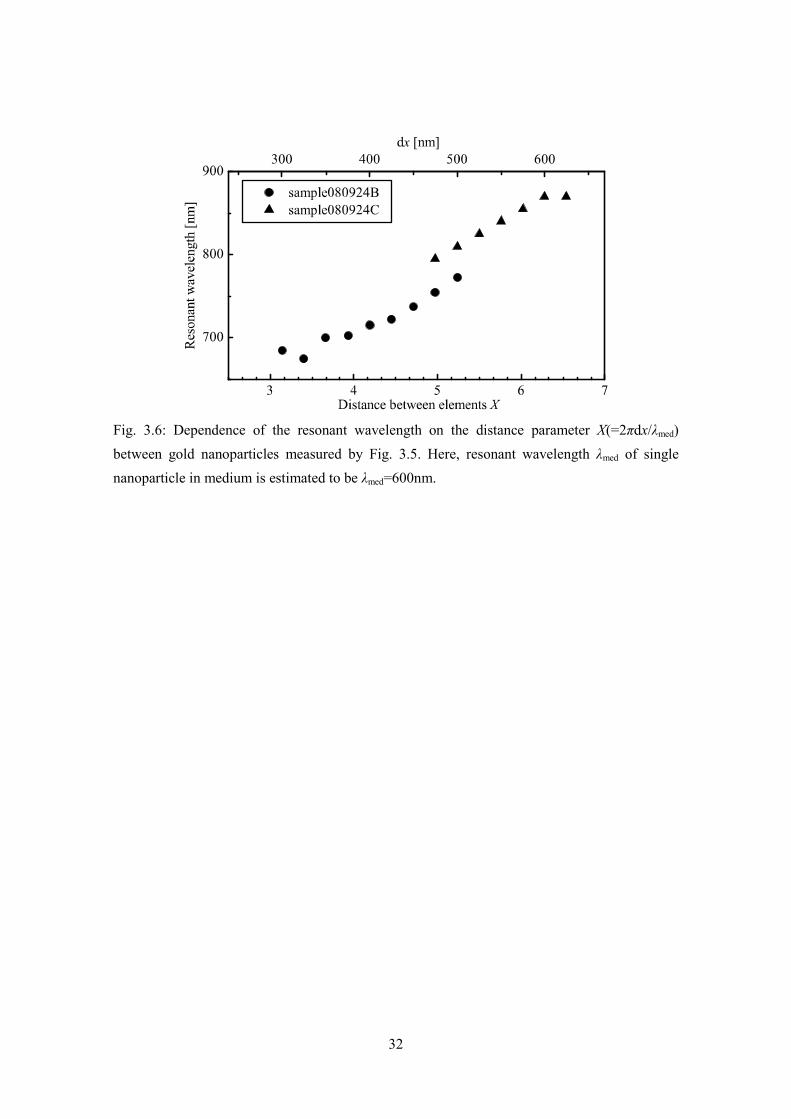
the dependence of the resonant wavelength on the distance parameter X=2πdx/λmed. Here,
λmed is the resonance wavelength of a single nanoparticle in the medium estimated as
follows. In the prediction shown in Fig. 3.2(a), the maximum red-shift is obtained when
dx(=r) is around dx=λmed. On the other hand, the maximum red-shift is observed at
around dx=600 nm in Fig. 3.5. Accordingly, the λmed was assumed to be λmed=600 nm.
With the increase of X in Fig. 3.6, the resonant wavelength red-shifts in the range of
~3<X<~6 (=300nm<dx<600nm). This phenomenon is consistent with the prediction
based on the coupled dipole model shown in Fig. 3.2(a). The linewidth was not
measured, because the shape of the transmission spectra becomes broad, asymmetric,
and two peaks appear for X>6(dx=600 nm).
As described in the Section 3.1, the range of 8<X<12 is the proper interparticle
distance for the evaluation of the LSPR of each particle from the spectroscopic
measurement of the array. When λmed is 600 nm, the range corresponds to
764nm<dx(=λmedX/2π)<1146nm. Based on these evaluations, the nanopattern spacing
was set to be dx=800nm in the resonant wavelength measurement of nanopattern shown
in Sec. 5.4.2.
Fig. 3.5: Dependence of the transmission spectra of gold nanoparticle array, embedded in a
sputter-deposited 100-nm-thick SiOx (n~1.44), on the distance between nanoparticles. The
substrates of Sample-080924B and Sample-080924C were different from each other.
32
Fig. 3.6: Dependence of the resonant wavelength on the distance parameter X(=2πdx/λmed)
between gold nanoparticles measured by Fig. 3.5. Here, resonant wavelength λmed of single
nanoparticle in medium is estimated to be λmed=600nm.
33
4. Design of nano optical Yagi-Uda antenna
The design of a nano optical Yagi-Uda antenna composed of a finite linear array of
nanoparticles will be considered in this chapter. In Section 4.1, the basics of the
Yagi-Uda antenna design will be summarized. Then in Section 4.2, the design of the
nano optical Yagi-Uda antennas will be described in detail. The design makes use of the
coupled dipole model described in Section 2.2. First, 2-element antennas consisting of a
feed element and either a reflector or a director will be investigated to confirm the
validity of the design concept that both the detuning and the spacing control the
function of the passive element. Based on the understanding of the characteristics of the
passive element, 3-element and 5-element antennas are designed to realize a desired
directivity. Finally, the effect of the material losses on the directivity will be discussed.
4.1. Basics of Yagi-Uda antenna design
4.1.1. Yagi-Uda antenna in radio frequency region
Since the invention by Dr. Yagi and Dr. Uda in 1926, Yagi-Uda antennas have widely
been used in the radio frequency (RF) bands [120]. Especially, in the range from VHF
(30-300 MHz) to UHF (300-3000 MHz), they have been used worldwide as the antenna
receiving the terrestrial broadcasting of television programs. Yagi-Uda antennas are
composed of feed, reflector, and director elements made of metal bars as illustrated in
Fig. 4.1. Feeding or extracting energy is performed only through the feed element. In
the radiation mode, the electromagnetic field emitted from the feed element induces
currents in the passive elements, which re-radiate the electromagnetic fields inducing a
current in the other element. Such an electromagnetic coupling between the elements
decides the oscillating currents in each element and the radiation from them.
The radiation from the multi-element antenna is the superposition of the radiations
from each element. Therefore the radiation pattern (directivity) of the antenna depends
on both the relative phase and the relative intensity of the radiation from each element.
The relative phase and intensity are controlled by the detuning of each element and the
spacing between the elements. Figure 4.2 qualitatively shows the impedance Z = R + jX
of a linear wire antenna of length L in air for the time dependence exp(-jωt). Note that
the sign in the time dependence used here is opposite to the convention in electric
engineering. The resonance occurs when L is slightly shorter than half the wavelength
34
λ/2. In the case of L longer/shorter than the resonance length, the reactance X is
negative/positive corresponding to inductive/capacitive response, while the phase of the
induced current is delayed/advanced with respect to the driving voltage. In RF range,
the elements cannot be considered to be infinitesimal. It is therefore practically
impossible to derive an analytical expression describing the radiation field of the
elements. As a result, the optimization of the RF Yagi-Uda antenna has been performed
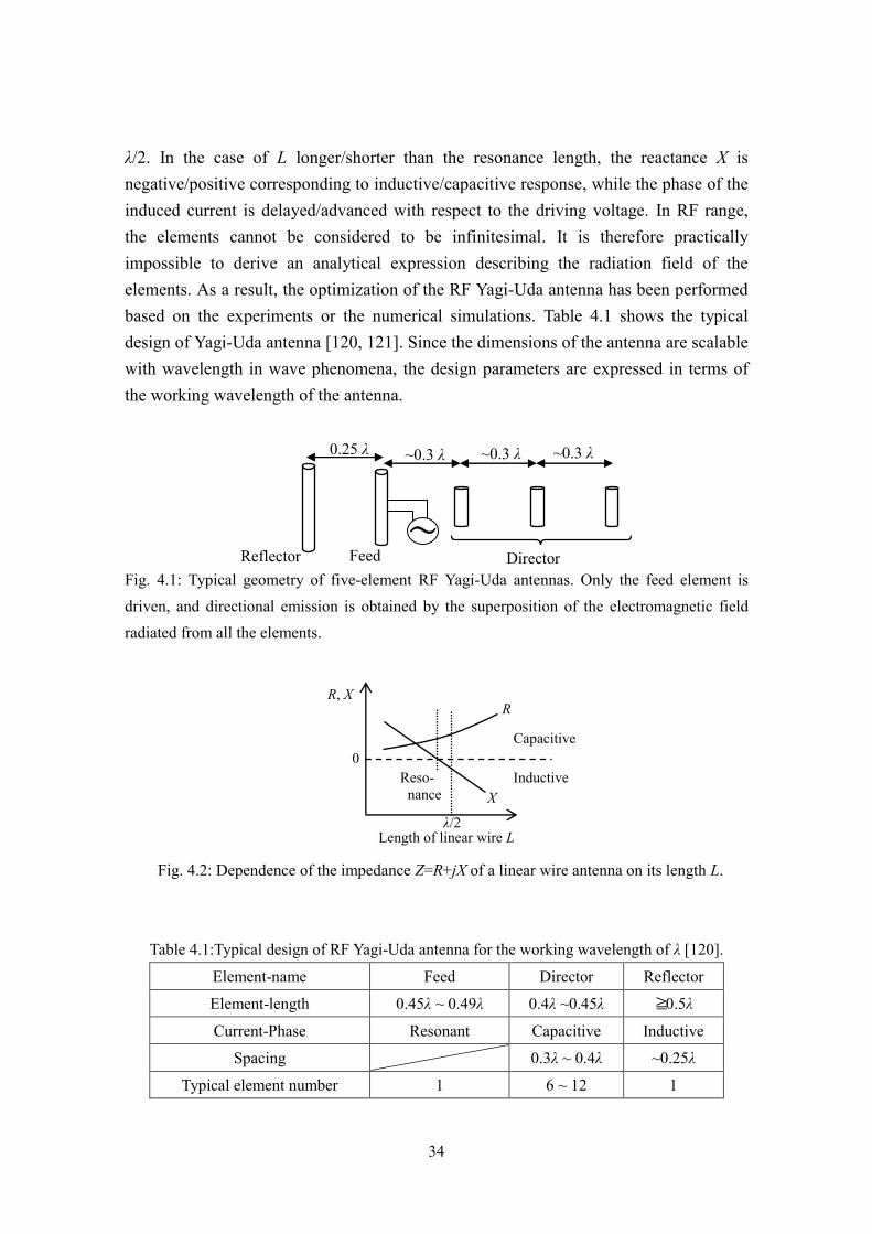
based on the experiments or the numerical simulations. Table 4.1 shows the typical
design of Yagi-Uda antenna [120, 121]. Since the dimensions of the antenna are scalable
with wavelength in wave phenomena, the design parameters are expressed in terms of
the working wavelength of the antenna.
Fig. 4.1: Typical geometry of five-element RF Yagi-Uda antennas. Only the feed element is
driven, and directional emission is obtained by the superposition of the electromagnetic field
radiated from all the elements.
Fig. 4.2: Dependence of the impedance Z=R+jX of a linear wire antenna on its length L.
Table 4.1:Typical design of RF Yagi-Uda antenna for the working wavelength of λ [120].
Element-name Feed Director Reflector
Element-length 0.45λ ~ 0.49λ 0.4λ ~0.45λ ≧0.5λ
Current-Phase Resonant Capacitive Inductive
Spacing 0.3λ ~ 0.4λ ~0.25λ
Typical element number 1 6 ~ 12 1
λ/2
0
Capacitive
Inductive
R
X
Reso-
nance
R, X
Length of linear wire L
Reflector Feed Director
0.25 λ ~0.3 λ ~0.3 λ ~0.3 λ
~

35
The feed element is resonantly driven at the working wavelength of λ with its length
set to be 0.45λ~ 0.49λ.
The director enhances and sharpens the radiation from the feed element in the
director side when the length is 0.4λ~0.45λ, which makes the impedance capacitive, i.e.
the phase of the current is advanced from the induced electric field. Typically, the
element spacing is set to be 0.3λ~0.4λ. Although increasing the number of directors can
enhance the directivity, the effect becomes small for larger number mostly due to the
finite losses in the metal bars. Typically, the number of directors is chosen to be 6 ~ 12
[120, 121].
The reflector reflects the radiation from the feed when the element length is set to be
~0.5λ, which makes the impedance inductive, i.e. the phase of the current is delayed
from that of the induced electric field. The optimum reflector-feed distance is ~0.25λ
[120, 121]. The increase of the number of reflectors has little effect on the gain, because
the reflection efficiency of one reflector is sufficiently high.
4.1.2. Optical Yagi-Uda antenna
Since the properties of metals in optical regime are significantly different from those
in RF range [38], the wavelength-scaled design of Yagi-Uda antenna is inappropriate,
particularly in the control of detuning of each element. In addition, the ohmic loss in
metals in optical regime is not negligibly small, which will suppress the interaction
between antenna elements. However, once appropriate antenna elements having the
same functions as those in RF Yagi-Uda antennas are found, Yagi-Uda antennas can be
constructed even in optical regime. That is because the wave propagation phenomena
are scalable. In particular, if the elements are dipolar type, the spatial arrangement of the
elements can be similar to that of RF Yagi-Uda antennas, since, as mentioned above, the
elements of RF Yagi-Uda antennas are designed around the half wavelength resonance
of metal bars at which the current (or charge) distribution along the wire is dipolar.
Therefore, it is important to find a dipolar type element with controllable resonance
and ohmic loss of acceptable level. As a candidate for such element, metal-dielectric
core-shell nanoparticle was proposed by Li et al. [124]. However, the metal-dielectric
core-shell structure is not easy to be fabricated and to be arranged spatially with precise
control of the resonance condition and position.
In this work, metal nanoparticles showing localized surface plasmon resonance
(LSPR) are utilized as the antenna elements. Metal nano patterns can be fabricated and

36
spatially arranged fairly easily by using electron beam lithography technique. In this
section, it is described how the LSPR in metal nanoparticles can be controlled for the
antenna elements, with a consideration on the effect of the material loss [122].
The dipolar response of a metal nanoparticle to the incident field Einexp(-iωt) is
described in Section 2.1.4 as follows.
(4.1)
(4.2)
(4.3)
(4.4)
(a) Detuning
Equation (4.1) and (4.2) indicate that the function of the element can be controlled by
adjusting the depolarization factor N as follows. Since the equivalent current is I ~ -iωd
~ Ein/(1+γmat-iδ), the element is inductive (capacitive) for δ>0 (δ<0). Table 4.2 shows
the relation between the depolarization factor N and the function of the elements. Since
Re(εr-1) is negative in the wavelength range considered here, the dipole is inductively
(capacitively) detuned when N is smaller (larger) than |Re(εr-1)|/| εr-1|2. In the case of
ellipsoidal nanoparticles, N is adjusted by controlling the aspect ratio of the
nanoparticles as described in Section 2.1.4. With the width in the minor axis fixed, a
metal rod, whose major axis is longer/shorter than the resonace having smaller/larger N
serves as the reflector/director, eventually in the same manner as in RF Yagi-Uda
antennas.
Table 4.2: Relation between the shape and the characteristics of LSP-based antenna elements.
Detuning
parameter δ
Characteristics
(Function)
Resonant wavelength of
the element
Depolarization
Factor N
> 0
Inductive
(Reflector) > λin
= 0
Resonance
(Feed) = λin
< 0
Capacitive
(Director) < λin
37
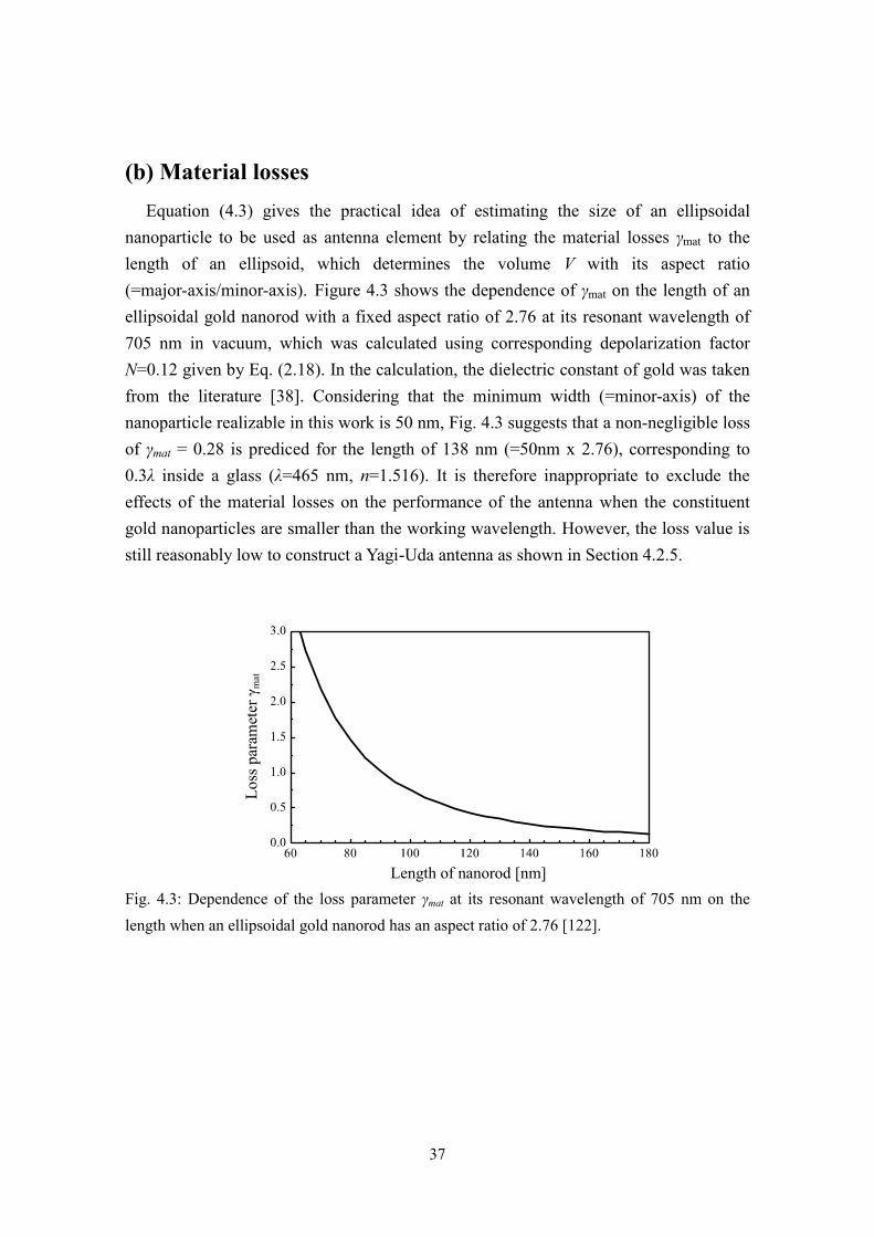
(b) Material losses
Equation (4.3) gives the practical idea of estimating the size of an ellipsoidal
nanoparticle to be used as antenna element by relating the material losses γmat to the
length of an ellipsoid, which determines the volume V with its aspect ratio
(=major-axis/minor-axis). Figure 4.3 shows the dependence of γmat on the length of an
ellipsoidal gold nanorod with a fixed aspect ratio of 2.76 at its resonant wavelength of
705 nm in vacuum, which was calculated using corresponding depolarization factor
N=0.12 given by Eq. (2.18). In the calculation, the dielectric constant of gold was taken
from the literature [38]. Considering that the minimum width (=minor-axis) of the
nanoparticle realizable in this work is 50 nm, Fig. 4.3 suggests that a non-negligible loss
of γmat = 0.28 is prediced for the length of 138 nm (=50nm x 2.76), corresponding to
0.3λ inside a glass (λ=465 nm, n=1.516). It is therefore inappropriate to exclude the
effects of the material losses on the performance of the antenna when the constituent
gold nanoparticles are smaller than the working wavelength. However, the loss value is
still reasonably low to construct a Yagi-Uda antenna as shown in Section 4.2.5.
Fig. 4.3: Dependence of the loss parameter γmat at its resonant wavelength of 705 nm on the
length when an ellipsoidal gold nanorod has an aspect ratio of 2.76 [122].
Loss param
eter γ
mat
Length of nanorod [nm]
38
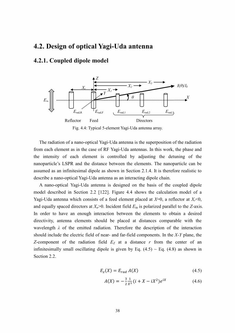
4.2. Design of optical Yagi-Uda antenna
4.2.1. Coupled dipole model
Fig. 4.4: Typical 5-element Yagi-Uda antenna array.
The radiation of a nano-optical Yagi-Uda antenna is the superposition of the radiation
from each element as in the case of RF Yagi-Uda antennas. In this work, the phase and
the intensity of each element is controlled by adjusting the detuning of the
nanoparticle’s LSPR and the distance between the elements. The nanoparticle can be
assumed as an infinitesimal dipole as shown in Section 2.1.4. It is therefore realistic to
describe a nano-optical Yagi-Uda antenna as an interacting dipole chain.
A nano-optical Yagi-Uda antenna is designed on the basis of the coupled dipole
model described in Section 2.2 [122]. Figure 4.4 shows the calculation model of a
Yagi-Uda antenna which consists of a feed element placed at X=0, a reflector at Xr<0,
and equally spaced directors at Xn>0. Incident field Ein is polarized parallel to the Z-axis.
In order to have an enough interaction between the elements to obtain a desired
directivity, antenna elements should be placed at distances comparable with the
wavelength λ of the emitted radiation. Therefore the description of the interaction
should include the electric field of near- and far-field components. In the X-Y plane, the
Z-component of the radiation field EZ at a distance r from the center of an
infinitesimally small oscillating dipole is given by Eq. (4.5) ~ Eq. (4.8) as shown in
Section 2.2.
(4.5)
(4.6)
Erad,R Erad,F Erad,1 Erad,2 Erad,3
Z
X θ
Y
I(θ)/IF
Ein
Reflector Feed Directors
Xr X1
X2
X3
39
(4.7)
(4.8)
Here, the parameters γmat and δ in Eq. (4.7) are defined in Eq. (4.2) and Eq. (4.3).
Following the working principle of an RF Yagi-Uda antenna, it is assumed that the
incident field Ein is injected only into the resonantly driven feed at the wavelength λ.
Additionally, the feed is assumed to be unaffected by other elements. Therefore the
amplitude Erad of the field emitted from the feed element is given by EF = Ein/(1+γmat).
On the other hand, each passive element is driven by the radiation from all the other
elements. As a result, the radiation field of the n-th passive element Erad, n is given by Eq.
(4.9).
(4.9)
Hence, Erad, n is determined by solving the simultaneous equations for all the elements
except for the feed.
Following the traditional way of the radio frequency study [120], directivity of an
antenna is described in terms of the emission intensity of the antenna normalized by the
IF of the feed element, as given by Eq. (4.10).
(4.10)
Here θ is the angle between the antenna axis and the emission direction in the X-Y plane
determined in Fig. 4.4. In the following consideration, at first, material losses γmat are
not included to simplify the investigation. Later, the effect of material losses on the
emission pattern of an antenna is considered.
40
4.2.2. Two-element antenna
Two-element antennas consisting of a feed element and a passive element is
considered in this section to investigate how the functionality of the passive element
depends on its detuning and the distance from the feed.
(a) Dependence of the functionality on the detuning of passive element
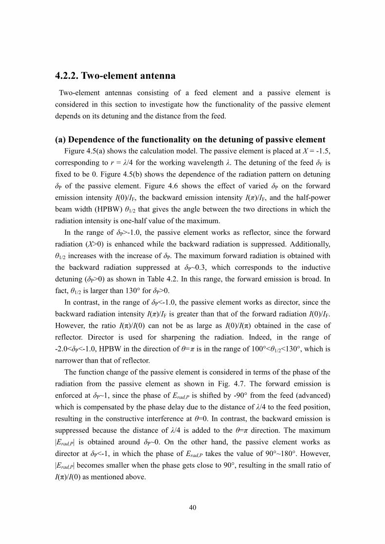
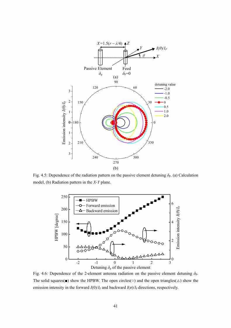
Figure 4.5(a) shows the calculation model. The passive element is placed at X = -1.5,
corresponding to r = λ/4 for the working wavelength λ. The detuning of the feed δF is
fixed to be 0. Figure 4.5(b) shows the dependence of the radiation pattern on detuning
δP of the passive element. Figure 4.6 shows the effect of varied δP on the forward
emission intensity I(0)/IF, the backward emission intensity I(π)/IF, and the half-power
beam width (HPBW) θ1/2 that gives the angle between the two directions in which the
radiation intensity is one-half value of the maximum.
In the range of δP>-1.0, the passive element works as reflector, since the forward
radiation (X>0) is enhanced while the backward radiation is suppressed. Additionally,
θ1/2 increases with the increase of δP. The maximum forward radiation is obtained with
the backward radiation suppressed at δP~0.3, which corresponds to the inductive
detuning (δP>0) as shown in Table 4.2. In this range, the forward emission is broad. In
fact, θ1/2 is larger than 130° for δP>0.
In contrast, in the range of δP<-1.0, the passive element works as director, since the
backward radiation intensity I(π)/IF is greater than that of the forward radiation I(0)/IF.
However, the ratio I(π)/I(0) can not be as large as I(0)/I(π) obtained in the case of
reflector. Director is used for sharpening the radiation. Indeed, in the range of
-2.0<δP<-1.0, HPBW in the direction of θ=π is in the range of 100°<θ1/2<130°, which is
narrower than that of reflector.
The function change of the passive element is considered in terms of the phase of the
radiation from the passive element as shown in Fig. 4.7. The forward emission is
enforced at δP~1, since the phase of Erad,P is shifted by -90° from the feed (advanced)
which is compensated by the phase delay due to the distance of λ/4 to the feed position,
resulting in the constructive interference at θ=0. In contrast, the backward emission is
suppressed because the distance of λ/4 is added to the θ=π direction. The maximum
|Erad,P| is obtained around δP~0. On the other hand, the passive element works as
director at δP<-1, in which the phase of Erad,P takes the value of 90°~180°. However,
|Erad,P| becomes smaller when the phase gets close to 90°, resulting in the small ratio of
I(π)/I(0) as mentioned above.
41
(a)
(b)
Fig. 4.5: Dependence of the radiation pattern on the passive element detuning δP. (a) Calculation
model, (b) Radiation pattern in the X-Y plane.
Fig. 4.6: Dependence of the 2-element antenna radiation on the passive element detuning δP.
The solid squares(■) show the HPBW. The open circles(○) and the open triangles(△) show the
emission intensity in the forward I(0)/IF and backward I(π)/IF directions, respectively.
Detuning δp of the passive element
HP
BW
[deg
ree]
Em
issi
on
in
tensi
ty I
(θ)/
I F
Em
issi
on i
nte
nsi
ty I
(θ)/
I F
Z
Feed
δF=0
Passive Element
δp
X
Y
X =1.5(r ~ λ/4)
θ
I(θ)/IF

42
Fig. 4.7: Dependence of the radiation from the passive element on the passive element detuning
δP. The amplitude and the phase are relative to those of the feed element.
(b) Dependence of reflector characteristics on the element distance
Figure 4.8(a) shows the calculation model of the antenna which consists of a feed
placed at X=0 and a reflector at Xr<0. The feed is the same as that shown in Fig. 4.5(a)
and the reflector detuning δr is fixed to be zero to obtain the maximum radiation from
the reflector, as shown in the previous section. Figure 4.8(b) shows the dependence of
the antenna emission in the X-Y plane on the feed-reflector distance Xr. Figure 4.9
summarizes the effect of varying Xr on the forward radiation intensity I(0)/IF, the
backward radiation intensity I(π)/IF, and the HPBW of radiation. In the range of Xr<1.0,
where the near field term (1/X3) in Eq. (4.6) is dominant, both I(0)/IF and I(π)/IF
drastically increase with the decrease of Xr. However, the HPBW becomes broader than
150°. In contrast, the narrow HPBW less than 150° is obtained in the range of
1.0<Xr<2.0, in which I(0)/IF increases gradually with the decrease of Xr, while I(π)/IF is
suppressed. The minimum HPBW of 130° is obtained at Xr=1.4. The distance
corresponds to r~0.22λ which is almost the same as the optimum distance in RF
Yagi-Uda antennas shown in Table 4.1. Additionally, the side lobes (θ=90°, 270°) are
well suppressed as shown in Fig. 4.8(b).
Imag
inar
y p
art
of
Era
d,P
0.6 0.4 0.2 0 0.2
0.6
0.4
0.2
0
0.2
δP=2.5
δP =2.0
δP =1.5
δP =1.0
δP =0.5
δP = 0
δP = -0.5
δP = -1.0
δP = -1.5
δP = -2.0 δP = -2.5
Real part of Erad,P
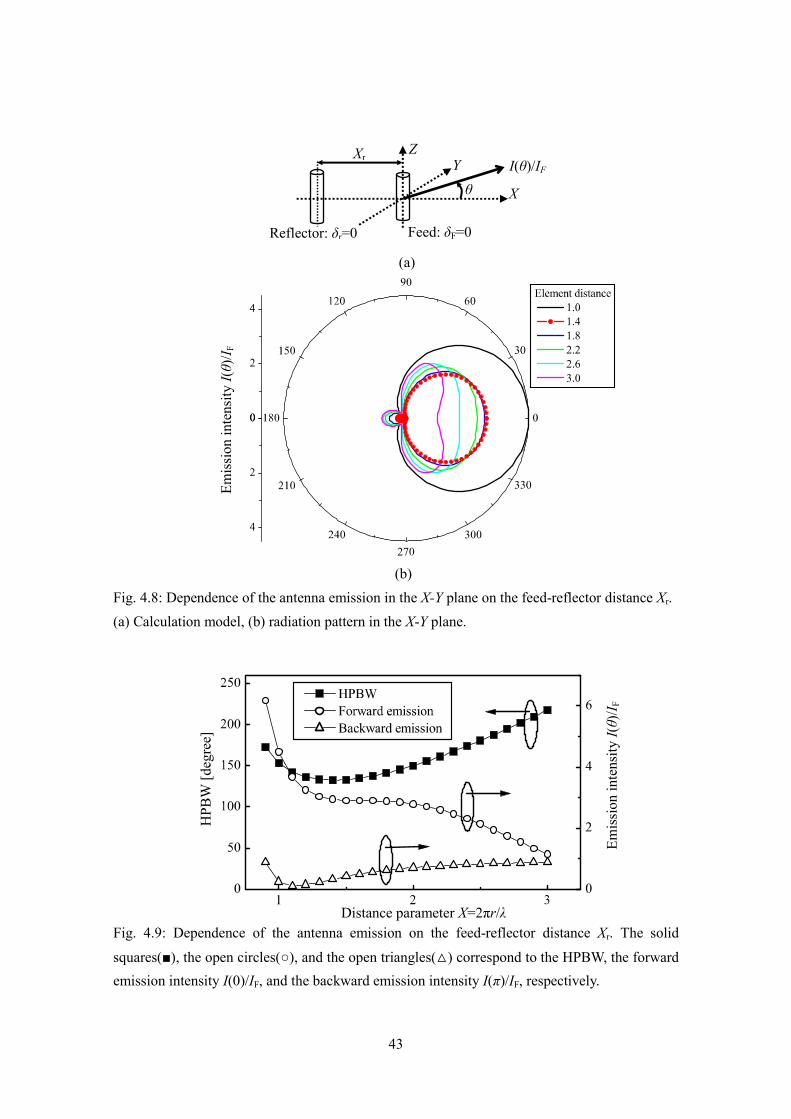
43
(a)
(b)
Fig. 4.8: Dependence of the antenna emission in the X-Y plane on the feed-reflector distance Xr.
(a) Calculation model, (b) radiation pattern in the X-Y plane.
Fig. 4.9: Dependence of the antenna emission on the feed-reflector distance Xr. The solid
squares(■), the open circles(○), and the open triangles(△) correspond to the HPBW, the forward
emission intensity I(0)/IF, and the backward emission intensity I(π)/IF, respectively.
Feed: δF=0
X
Z
Y
Xr
θ
I(θ)/IF
Reflector: δr=0
Distance parameter X=2πr/λ
HP
BW
[deg
ree]
Em
issi
on
in
tensi
ty I
(θ)/
I F
Em
issi
on i
nte
nsi
ty I
(θ)/
I F
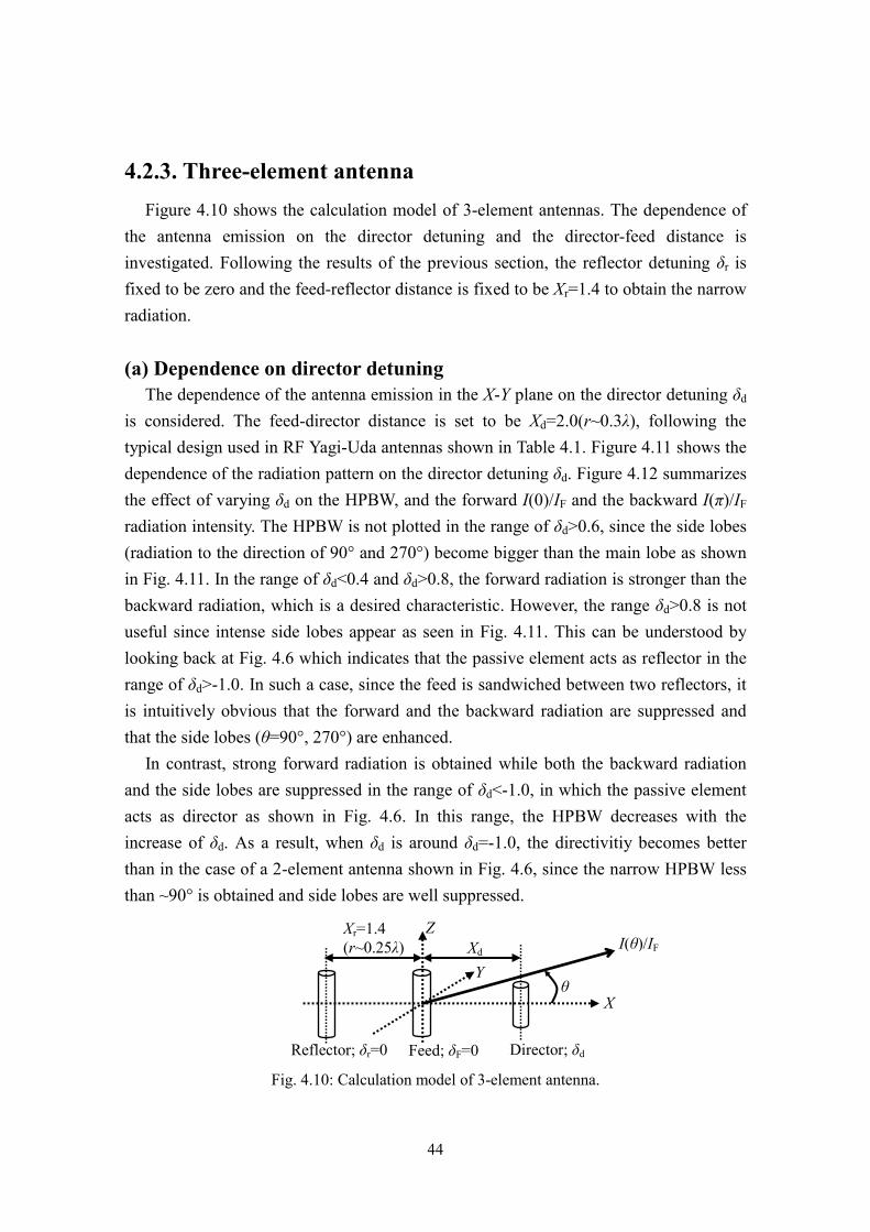
44
4.2.3. Three-element antenna
Figure 4.10 shows the calculation model of 3-element antennas. The dependence of
the antenna emission on the director detuning and the director-feed distance is
investigated. Following the results of the previous section, the reflector detuning δr is
fixed to be zero and the feed-reflector distance is fixed to be Xr=1.4 to obtain the narrow
radiation.
(a) Dependence on director detuning
The dependence of the antenna emission in the X-Y plane on the director detuning δd
is considered. The feed-director distance is set to be Xd=2.0(r~0.3λ), following the
typical design used in RF Yagi-Uda antennas shown in Table 4.1. Figure 4.11 shows the
dependence of the radiation pattern on the director detuning δd. Figure 4.12 summarizes
the effect of varying δd on the HPBW, and the forward I(0)/IF and the backward I(π)/IF
radiation intensity. The HPBW is not plotted in the range of δd>0.6, since the side lobes
(radiation to the direction of 90° and 270°) become bigger than the main lobe as shown
in Fig. 4.11. In the range of δd<0.4 and δd>0.8, the forward radiation is stronger than the
backward radiation, which is a desired characteristic. However, the range δd>0.8 is not
useful since intense side lobes appear as seen in Fig. 4.11. This can be understood by
looking back at Fig. 4.6 which indicates that the passive element acts as reflector in the
range of δd>-1.0. In such a case, since the feed is sandwiched between two reflectors, it
is intuitively obvious that the forward and the backward radiation are suppressed and
that the side lobes (θ=90°, 270°) are enhanced.
In contrast, strong forward radiation is obtained while both the backward radiation
and the side lobes are suppressed in the range of δd<-1.0, in which the passive element
acts as director as shown in Fig. 4.6. In this range, the HPBW decreases with the
increase of δd. As a result, when δd is around δd=-1.0, the directivitiy becomes better
than in the case of a 2-element antenna shown in Fig. 4.6, since the narrow HPBW less
than ~90° is obtained and side lobes are well suppressed.
Fig. 4.10: Calculation model of 3-element antenna.
Director; δd Reflector; δr=0 Feed; δF=0
I(θ)/IF
θ
Y
Xr=1.4
(r~0.25λ)
X
Xd
Z

45
Fig. 4.11: Dependence of antenna radiation in the X-Y plane on the director detuning δd.
Fig. 4.12: Dependence of 3-element antenna radiation on the director detuning δd. The solid
squares(■), the open circles(○), and the open triangles(△) correspond to the HPBW, the forward
emission intensity I(0)/IF, and the backward emission intensity I(π)/IF, respectively.
Director detuning δd
HP
BW
[deg
ree]
Em
issi
on i
nte
nsi
ty I
(θ)/
I F
Em
issi
on
in
ten
sity
I(θ
)/I F

46
(b) Dependence on Feed-Director distance
The dependence of the antenna emission in the X-Y plane on the feed-director
distance Xd is considered. Following the results of the previous section, the director
detuning is fixed to be δd=-1.0. Figure 4.13 shows the dependence of the emission
pattern on the feed-director distance Xd. Figure 4.14 summarizes the effects of varying
Xd on the HPBW, and the forward I(0)/IF and backward I(π)/IF emission intensity.
In the range of Xd<1.4, the forward emission and the HPBW decrease with the
decrease of Xd, while the backward radiation is suppressed.
In the range of 1.4<Xd<4.0, the HPBW is almost constant with θ1/2~80°, while the
ratio I(0)/I(π) increases with the increase of Xd. However, in the range of Xd>2.0, the
backward radiation becomes large. In addition, the side-lobes become larger gradually
with the increase of Xd as shown in Fig. 4.13. As a result, the antenna shows a good
directivity at Xd~2.0, where I(0)/I(π) is large while the side lobes are suppressed. Note
that the distance of Xd=2.0(r~0.3λ) is almost the same as the optimum director spacing
for RF Yagi-Uda antennas shown in Table 4.1.
Fig. 4.13: Dependence of 3-element antenna emission in the X-Y plane on the feed-director
distance Xd.
Em
issi
on i
nte
nsi
ty I
(θ)/
I F
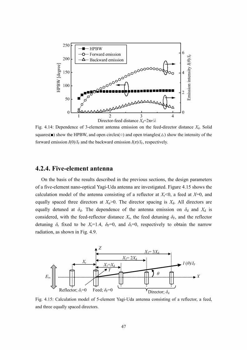
47
Fig. 4.14: Dependence of 3-element antenna emission on the feed-director distance Xd. Solid
squares(■) show the HPBW, and open circles(○) and open triangles(△) show the intensity of the
forward emission I(0)/IF and the backward emission I(π)/IF, respectively.
4.2.4. Five-element antenna
On the basis of the results described in the previous sections, the design parameters
of a five-element nano-optical Yagi-Uda antenna are investigated. Figure 4.15 shows the
calculation model of the antenna consisting of a reflector at Xr<0, a feed at X=0, and
equally spaced three directors at Xn>0. The director spacing is Xd. All directors are
equally detuned at δd. The dependence of the antenna emission on δd and Xd is
considered, with the feed-reflector distance Xr, the feed detuning δF, and the reflector
detuning δr fixed to be Xr=1.4, δF=0, and δr=0, respectively to obtain the narrow
radiation, as shown in Fig. 4.9.
Fig. 4.15: Calculation model of 5-element Yagi-Uda antenna consisting of a reflector, a feed,
and three equally spaced directors.
Reflector; δr=0 Feed; δF=0 Director; δd
Y
Z
θ
Xr X1=Xd
X2= 2Xd
X3= 3Xd
I (θ)/IF
Ein X
Director-feed distance Xd=2πr/λ
HP
BW
[d
egre
e]
Em
issi
on
in
ten
sity
I(θ
)/I F
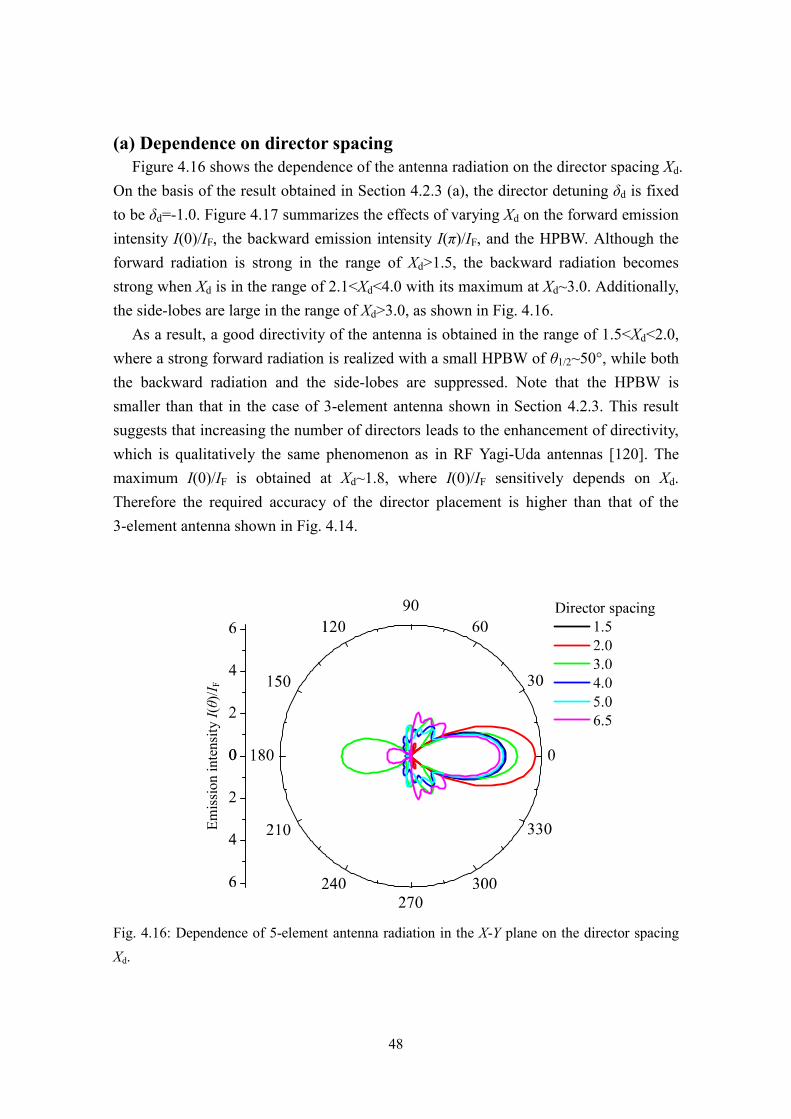
48
(a) Dependence on director spacing
Figure 4.16 shows the dependence of the antenna radiation on the director spacing Xd.
On the basis of the result obtained in Section 4.2.3 (a), the director detuning δd is fixed
to be δd=-1.0. Figure 4.17 summarizes the effects of varying Xd on the forward emission
intensity I(0)/IF, the backward emission intensity I(π)/IF, and the HPBW. Although the
forward radiation is strong in the range of Xd>1.5, the backward radiation becomes
strong when Xd is in the range of 2.1<Xd<4.0 with its maximum at Xd~3.0. Additionally,
the side-lobes are large in the range of Xd>3.0, as shown in Fig. 4.16.
As a result, a good directivity of the antenna is obtained in the range of 1.5<Xd<2.0,
where a strong forward radiation is realized with a small HPBW of θ1/2~50°, while both
the backward radiation and the side-lobes are suppressed. Note that the HPBW is
smaller than that in the case of 3-element antenna shown in Section 4.2.3. This result
suggests that increasing the number of directors leads to the enhancement of directivity,
which is qualitatively the same phenomenon as in RF Yagi-Uda antennas [120]. The
maximum I(0)/IF is obtained at Xd~1.8, where I(0)/IF sensitively depends on Xd.
Therefore the required accuracy of the director placement is higher than that of the
3-element antenna shown in Fig. 4.14.
Fig. 4.16: Dependence of 5-element antenna radiation in the X-Y plane on the director spacing
Xd.
Em
issi
on
inte
nsi
ty I
(θ)/
I F

49
Fig. 4.17: Dependence of 5-element antenna emission in the X-Y plane on the director spacing
Xd. Open circles(○), open triangles(△), and solid squares(■) show the forward emission
intensity I(0)/IF, the backward emission intensity I(π)IF, and the HPBW, respectively. The
forward radiation is strong while the backward radiation and side lobes are suppressed in the
shadow area.
(b) Dependence on director detuning
Following the results of the previous section, the director spacing is fixed to be
Xd=2.0 to obtain the strong forward emission with the backward radiation suppressed.
Figure 4.18 shows the dependence of the radiation pattern on the director detuning δd.
Figure 4.19 summarizes the effect of varying δd on the HPBW, the emission intensity in
the directions of the forward I(0)/IF and the backward I(π)/IF.
In the range of δd<-1.2, the forward radiation increases with the increase of δd. The
backward radiation is suppressed. The HPBW gradually decreases with the increase of
δd. The maximum I(0)/IF is obtained at δd =-1.2 with the HPBW of ~60°. On the other
hand, the minimum backward radiation is obtained around δd=-0.9 where the forward
radiation is still strong.
As a result, a best directivity is obtained in the range of -1.2<δd<-0.9, since the
forward radiation is strong, and both the backward radiation and the side-lobes are well
suppressed as shown in Fig. 4.18. However, the forward radiation steeply decreases
with the increase of δd in the range of δd>-1.2, which suggests that more precise
detuning control than that in 3-element antenna is necessary to obtain strong forward
radiation. Therefore, in experiment, it may be better not to choose δd close to -0.9.
Director spacing Xd=2πr/λ
HP
BW
[d
egre
e]
Em
issi
on
in
ten
sity
I(θ
)/I F
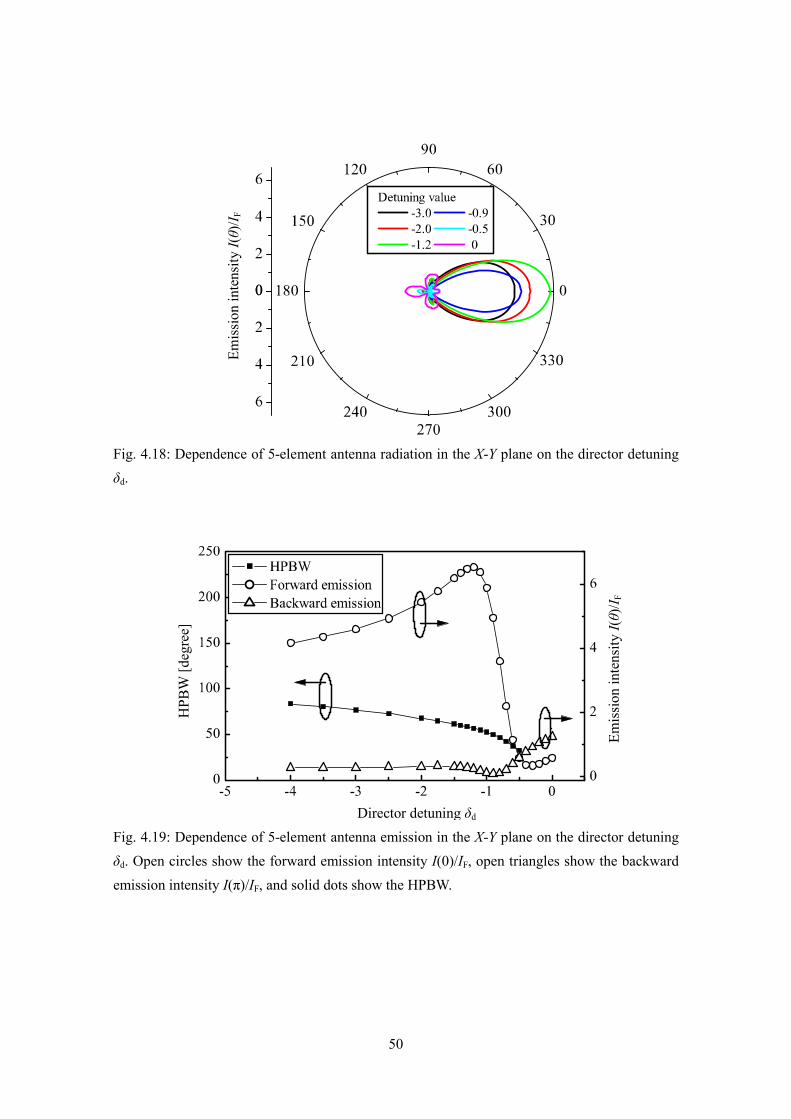
50
Fig. 4.18: Dependence of 5-element antenna radiation in the X-Y plane on the director detuning
δd.
Fig. 4.19: Dependence of 5-element antenna emission in the X-Y plane on the director detuning
δd. Open circles show the forward emission intensity I(0)/IF, open triangles show the backward
emission intensity I(π)/IF, and solid dots show the HPBW.
Em
issi
on
in
ten
sity
I(θ
)/I F
Director detuning δd
HP
BW
[deg
ree]
Em
issi
on i
nte
nsi
ty I
(θ)/
I F

51
4.2.5. Effect of material losses on the directivity
The effect of material losses on the 5-element antenna emission is considered, since
the losses are not negligible in the optical response of metals as mentioned in Section
4.1.2(b). The calculation model is the same as that shown in Fig. 4.15. Following the
previous results, director spacing Xd and director detuning δd is fixed to be Xd=2.0 and
δd=-1.0 to obtain the strong forward emission. In addition, the reflector detuning δr is
fixed to be zero and the feed-reflector distance is fixed to be Xr=1.4 to suppress the
backward radiation. The material losses γmat of all antenna elements are assumed to be
the same. The radiation losses, γmat=1.0 may be a kind of limit to realize Yagi-Uda
antennas relying on the coupling between the elements.
Figure 4.20 shows the effect of the material losses γmat on the antenna emission. The
black line shows the results without the loss. Obviously, the radiation becomes weak
owing to the presence of the material loss. In particular, the directionality I(0)/IF
decreases to ~1/3 even when γmat=0.5, indicating that the interaction between elements
becomes weaker than in the case without γmat. The effect of weakened interaction on the
directivity can also be seen as the shallower depth of the dip (θ~±45°, ±100°). All these
results come from the decrease of the radiation from each element due to the material
losses.
However, the emission pattern still shows such a good directivity that the forward
radiation is stronger than the backward radiation, and that the emission pattern is narrow.
Therefore, it is concluded that the Yagi-Uda antenna can be constructed in optical
regime as long as the material loss γmat is smaller than 1.

52
(a)
(b)
Fig. 4.20: Effect of the material losses on the 5-element antenna emission. (a) Overall view, (b)
close-up. The black line shows the result without material losses, and the red and the green lines
show the results including material losses of γmat=0.5 and γmat=1.0, respectively. The other
antenna parameters are Xr=1.4, δr=0, Xd=2.0, and δd=-1.0.
Em
issi
on
in
ten
sity
I(θ
)/I F
E
mis
sion i
nte
nsi
ty I
(θ)/
I F
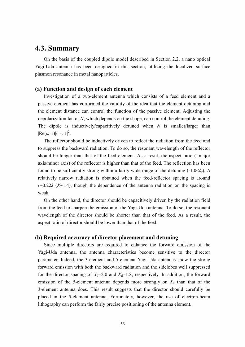
53
4.3. Summary
On the basis of the coupled dipole model described in Section 2.2, a nano optical
Yagi-Uda antenna has been designed in this section, utilizing the localized surface
plasmon resonance in metal nanoparticles.
(a) Function and design of each element
Investigation of a two-element antenna which consists of a feed element and a
passive element has confirmed the validity of the idea that the element detuning and
the element distance can control the function of the passive element. Adjusting the
depolarization factor N, which depends on the shape, can control the element detuning.
The dipole is inductively/capacitively detuned when N is smaller/larger than
|Re(εr-1)|/| εr-1|2.
The reflector should be inductively driven to reflect the radiation from the feed and
to suppress the backward radiation. To do so, the resonant wavelength of the reflector
should be longer than that of the feed element. As a resut, the aspect ratio (=major
axis/minor axis) of the reflector is higher than that of the feed. The reflection has been
found to be sufficiently strong within a fairly wide range of the detuning (-1.0<δr). A
relatively narrow radiation is obtained when the feed-reflector spacing is around
r~0.22λ (X~1.4), though the dependence of the antenna radiation on the spacing is
weak.
On the other hand, the director should be capacitively driven by the radiation field
from the feed to sharpen the emission of the Yagi-Uda antenna. To do so, the resonant
wavelength of the director should be shorter than that of the feed. As a result, the
aspect ratio of director should be lower than that of the feed.
(b) Required accuracy of director placement and detuning
Since multiple directors are required to enhance the forward emission of the
Yagi-Uda antenna, the antenna characteristics become sensitive to the director
parameter. Indeed, the 3-element and 5-element Yagi-Uda antennas show the strong
forward emission with both the backward radiation and the sidelobes well suppressed
for the director spacing of Xd=2.0 and Xd=1.8, respectively. In addition, the forward
emission of the 5-element antenna depends more strongly on Xd than that of the
3-element antenna does. This result suggests that the director should carefully be
placed in the 5-element antenna. Fortunately, however, the use of electron-beam
lithography can perform the fairly precise positioning of the antenna element.

54
The forward radiation also depends on the director detuning δd in the antennas with
larger number of directors. In particular, the forward radiation decreases steeply when
δd > -1 in the case of 5-element antenna. Contrary to the case of controlling the
element position, precise control of detuning is not an easy task since the shape of the
nanoparticle determines the detuning. Precise control of the shape in nanoscale is
difficult. Therefore, practically, the detuning parameter δd should be chosen not to be
too close to δd=-1 where the function of the antenna element drastically changes.
Accordingly, in the case of 5-element antenna, director detuning in the range of
-2<δd<-1 may be an appropriate choice.
As a consequence, for example, appropriate directivity (I(0)/IF = 6.52, I(π)/IF = 0.24,
HPBW = 56.7°) has been obtained for element parameters of reflector (δr = 0, Xr = 1.4),
feed (δf = 0), and director (δd = -1.2, Xd = 2.0). The emission pattern is shown as a
green line in Fig. 4.18.
(c) Effect of material losses
It has been confirmed that even if the material losses are comparable to the
radiation losses, the 5-element Yagi-Uda antenna shows directivity. However, due to
the material losses, the radiation from the antenna element decreases. As a result, the
forward radiation decreases to about one third of that without the material losses.
Additionally, the depth of the dips in the emission pattern becomes shallower than that
without the material losses. Therefore, the material losses should be smaller than the
radiation losses as much as possible to realize a good Yagi-Uda antenna with strong
directivity.
Although the material losses of silver are less than those of gold, gold has been
chosen as the antenna elements in this work. That is because silver is so easily
oxidized that it is more difficult to handle.
The proper size of gold nanoparticles to be used as antenna elements has been
estimated by relating the material losses to the aspect ratio of the nanoparticles. As a
result, the gold nanoparticles with the length longer than 50 nm, with the fixed width
and the thickness of 50 nm have been found to have the material losses less than 0.5
relative to the radiation loss.
55
5. Nano-optical Yagi-Uda antenna: Experiment The realizability of directional control of light by a nano-optical Yagi-Uda antenna
consisting of gold nanoparticles was experimentally examined as follows [123]. On the
basis of the design obtained in Chapter 4, antennas were fabricated by means of electron
beam lithography (EBL) and gold lift-off process. First, the radiation pattern of the
single element antennas was measured to confirm the validity of driving method of the
antenna and the adequacy of the measurement set-up. Second, the radiation pattern of a
2-element antenna consisting of a feed and a reflector/director was measured to confirm
the idea that the element detuning can control the function of the passive element. After
that, the radiation pattern of a 5-element Yagi-Uda antenna was measured to
demonstrate the directional control of light.
5.1. Nano pattern fabrication
Table 5.1 shows the main specifications of the EBL equipment used in this work. The
realizable minimum width of the exposed patterns is around 50 nm. The typical
exposure conditions of the EBL used in this work were a beam current of 40 pA and
dose of 250-390 μC/cm2.
Figure 5.1 shows the sample fabrication process. The details are given in Appendix II.
The antennas were fabricated on a glass substrate (n=1.51). To put the antenna in a
uniform medium for ensuring the interaction between the elements, the antenna was
sandwiched between sputter-deposited SiOx films of refractive index n~1.44. To obtain
fine resist patterns with reverse-tapered cross-section, which is appropriate for the
subsequent lift-off process, the bi-layer resist process was applied in this work [128,
129]. The upper and lower layer of the bi-layer resist was ZEP-520A7 (Zeon
Corporation) and PMMA (950PMMA-A2, MicroChem Corp.), respectively.
Additionally, a conductive layer (ESPACER 300Z Showa Denko K.K.) was spin-coated
on the ZEP-520A7 layer to avoid the charge-up during the electron beam exposure.
After the exposure, at first, the ESPACER layer was removed by a dip-treatment in
de-ionized water. After the development of the ZEP-520A7 layer, dip treatment was
applied with rinse solution. At the same time, PMMA layer was etched by the rinse
solution [129]. After that, the sample was rinsed with the de-ionized water, which was
subsequently removed by a N2-blow. Next, a gold film was deposited in a vaccum
evaporator with a rate of 0.1 nm/sec. By means of a lift-off process, the gold film was
removed, leaving the antenna patterns. Finally, SiOx film was deposited on the sample

56
to cover the antenna pattern. Figure 5.2 shows a SEM image of the fabricated gold nano
pattern. The nano pattern with the width of 52 nm and the length of 68 nm was
obtained.
Table 5.1: Main specifications of the electron beam lithography equipment
(ELIONIX Co.; ELS-3700) used in this work.
Electron
Gun Type
Max acceleration
voltage
Minimum
beam radius
Minimum
line width
LaB6 30 kV 6 nm ~50 nm
Fig. 5.1: The flow chart of the sample fabrication process by the electron beam lithography with
bi-layer resist process [128, 129], and subsequent gold lift-off process.
Rinse PMMA
N2-Blow
Gold deposition
Gold lift-off
SiOx-deposition
~ 100 nm
ESPACER-300Z ~ 5 nm
ZEP-520 A7 ~ 180 nm
PMMA 950K ~ 50 nm
SiOx ~ 100 nm
Glass-substrate
Electron beam exposure
ESPACER removal
ZEP-520 development
Rinse ZEP-520
Etching PMMA

57
Fig. 5.2: An example of the SEM image of the gold nano pattern.
5.2. Driving method of antenna
The antenna design obtained in Chapter 4 assumed that the incident power would be
injected only into the feed element. In order to realize the assumed situation, the
polarization dependence of the nanorod response was used in this work [123]. Figure
5.3 shows the top view of the antenna layout. The feed element was tilted by 45 degrees
towards the antenna axis, and driven by the incident field polarized parallel to the
antenna axis (X). In principle, owing to this diagonal alignment, the feed converts a part
of the incident field into the one polarized along the major axis (Y) of the passive
elements. As a result, the converted field drives the passive elements. Since the major
axes of the passive elements are parallel with each other, all passive elements interact
well with each other. Thus, the antenna is driven only through the feed element. In the
measurement, only the Y-polarized radiation was detected.
Fig. 5.3: Top view of a 5-element nano optical Yagi-Uda antenna.
When the feed element was arranged to be tilted, the edge of the feed became close
to the neighboring element as shown in Fig. 5.3. The effect of it on the directivity of the
antenna emission was examined by a finite difference time domain (FDTD) method
using commercial software (Fullwave, Rsoft. Co.,). Figure 5.4(a) shows the calculation
model of a feed-reflector antenna. The feed was modeled by a rectangular with the
width and thickness of 50 nm, capped by a half circle with the radius of 25 nm. The
total length of the feed is 106 nm. The shape of the reflector was the same as that of the
feed, except that the length was set to be 125 nm, following the prediction given in the
X (Antenna Axis)
Edetect
Ein
Reflector Feed Directors
45°
Y Z
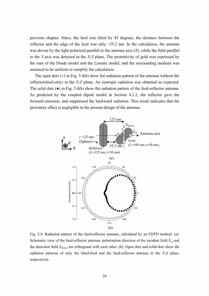
58
previous chapter. Since, the feed was tilted by 45 degrees, the distance between the
reflector and the edge of the feed was only ~55.2 nm. In the calculation, the antenna
was driven by the light polarized parallel to the antenna axis (X), while the field parallel
to the Y-axis was detected in the X-Z plane. The permittivity of gold was expressed by
the sum of the Drude model and the Lorentz model, and the surrounding medium was
assumed to be uniform to simplify the calculation.
The open dots (○) in Fig. 5.4(b) show the radiation pattern of the antenna without the
reflector(feed-only) in the X-Z plane. An isotropic radiation was obtained as expected.
The solid dots (●) in Fig. 5.4(b) show the radiation pattern of the feed-reflector antenna.
As predicted by the coupled dipole model in Section 4.2.2, the reflector gave the
forward emission, and suppressed the backward radiation. This result indicates that the
proximity effect is negligible in the present design of the antenna.
(a)
(b)
Fig. 5.4: Radiation pattern of the feed-reflector antenna, calculated by an FDTD method. (a):
Schematic view of the feed-reflector antenna: polarization direction of the incident field Ein and
the detection field Edetect are orthogonal with each other. (b): Open dots and solid dots show the
radiation patterns of only the tilted-feed and the feed-reflector antenna in the X-Z plane,
respectively.
Z
X
Y
Antenna axis Ein
Edetect
125 nm
55.2 nm
r =25 nm
(Sphere)
Reflector
(L=125 nm, t=50 nm)
Feed
(L=106 nm, t=50 nm)

59
5.3. Measurement set-up
5.3.1. Evaluation of resonant wavelength
The resonant wavelength of the localized surface plasmon resonance of the
fabricated nano patterns was evaluated by measuring the transmission spectra. Figure
5.5 shows the measurement set-up used in this work. The light source was a halogen
lamp (PHILIPS, 50 W). The FWHM of the focus spot size at the sample position was
measured to be about 30 μm with a knife-edge method. The polarizers controlled the
polarization of the incident and the transmitted light.
Fig. 5.5: Schematic diagram of the transmittion spectroscopy set-up.
5.3.2. Measurement of radiation pattern
Figure 5.6 shows the set-up for measuring the radiation pattern of the optical
antennas. The sample was set on an equilateral dispersive prism (BK7, n=1.517), and
covered by a hemispherical lens (radius=5 mm, BK7, n=1.517). An index-matching oil
(Cargille Labs, Type FF, n=1.479) was used at the interfaces. The antennas were driven
by a laser diode (10 mW) at 662 nm through a polarizer. The focus size was 15 μm by
36 μm, measured with a knife-edge method without the prism. The power radiated from
the antennas was detected in the X-Z plane, orthogonal to the substrate including the
antenna axis, by a silicon photodiode through a polarizer. A slit with the width of 2 mm
was set in front of the silicon photodiode. Since the distance between the antenna and
the slit was 40 mm, the angular resolution was 2.86 degrees.
Figure 5.7 shows the photos of the measurement set-up. To avoid the blocking of the
radiation from the antenna, the fixture of the sample holding was specially designed as
shown in Fig. 5.7(c). Thus this measurement set-up was able to measure the radiation
pattern of the antenna from 0 to 180 degrees.
Halogen Lamp
(50W)
Lens
Pin-Hole
Lens Objective-Lens
(x 20)
Sample
Lens Lens
Optical Fiber
φ=1.0mm
CCD
Spectrometer
Polarizer Polarizer
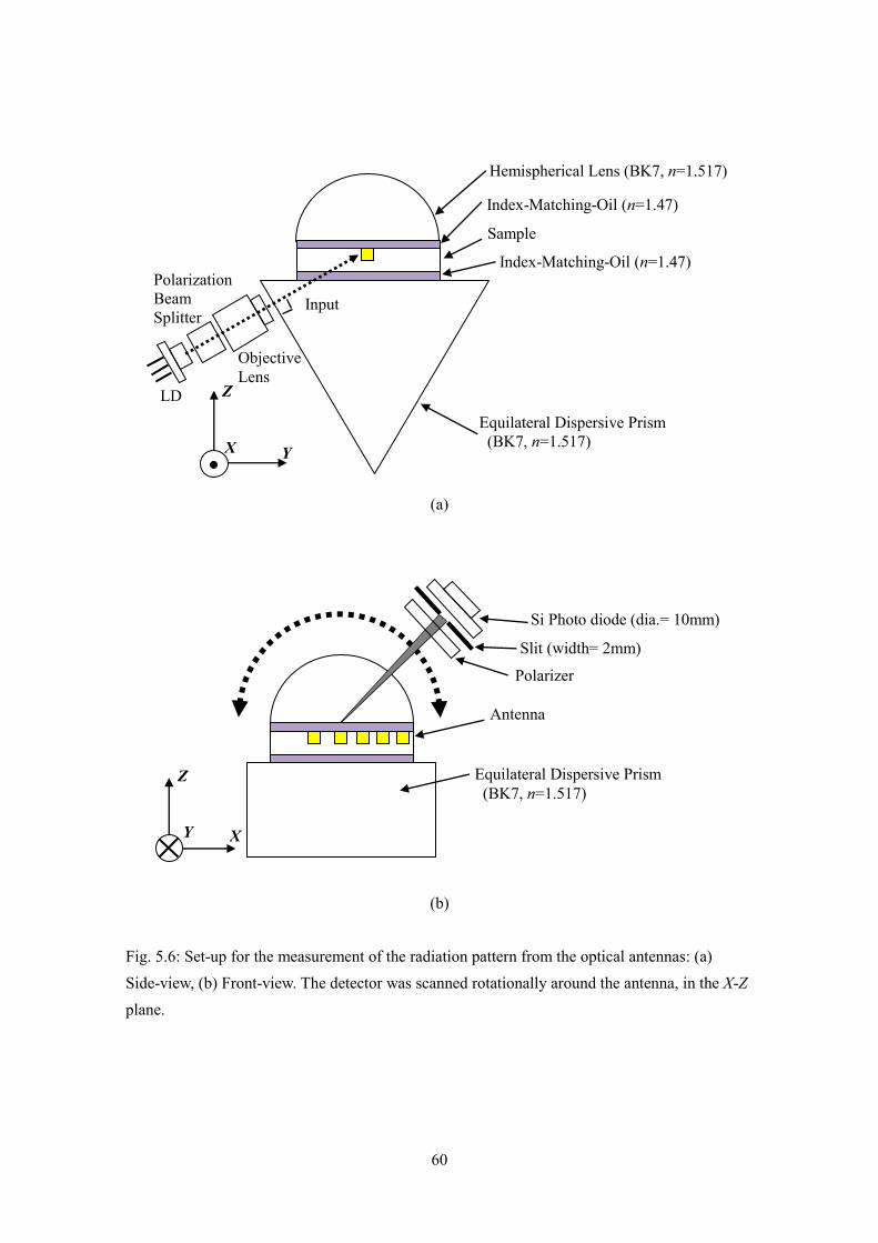
60
(a)
(b)
Fig. 5.6: Set-up for the measurement of the radiation pattern from the optical antennas: (a)
Side-view, (b) Front-view. The detector was scanned rotationally around the antenna, in the X-Z
plane.
Z
Y X
Equilateral Dispersive Prism
(BK7, n=1.517)
Antenna
Slit (width= 2mm)
Polarizer
Si Photo diode (dia.= 10mm)
Y
Z
X
Equilateral Dispersive Prism
(BK7, n=1.517)
Input
LD
Polarization
Beam
Splitter
Objective
Lens
Hemispherical Lens (BK7, n=1.517)
Index-Matching-Oil (n=1.47)
Sample
Index-Matching-Oil (n=1.47)

61
(a)
(b)
(c)
Fig. 5.7: Photos of the radiation pattern measurement set-up; (a) top view, (b) front view of the
sample holder, and (c) the schematic view of the fixture of the sample holding. The detector was
moved along the white-dots in the X-Z plane. Since the detection plane, which was parallel to
the antenna axis, had no blocking, the detector was able to measure the radiation pattern of the
antennas from 0 to 180 degrees. A polarizer was set in front of the photo diode to choose the
polarization direction of the detection field.
Polarizer
Objective-Lens
(x10)
Detection-plane
Sample Hemispherical
lens
Y
X
Z
Detector-rotation
plane
X
Z Y
Sample
Photo diode
Polarizer
Equilateral
dispersive prism
Objective-Lens
(x 10)
Hemispherical lens Sample
Equilateral dispersive prism
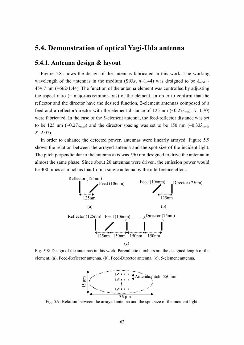
62
5.4. Demonstration of optical Yagi-Uda antenna
5.4.1. Antenna design & layout
Figure 5.8 shows the design of the antennas fabricated in this work. The working
wavelength of the antennas in the medium (SiOx, n~1.44) was designed to be λmed ~
459.7 nm (=662/1.44). The function of the antenna element was controlled by adjusting
the aspect ratio (= major-axis/minor-axis) of the element. In order to confirm that the
reflector and the director have the desired function, 2-element antennas composed of a
feed and a reflector/director with the element distance of 125 nm (~0.27λmed, X=1.70)
were fabricated. In the case of the 5-element antenna, the feed-reflector distance was set
to be 125 nm (~0.27λmed) and the director spacing was set to be 150 nm (~0.33λmed,
X=2.07).
In order to enhance the detected power, antennas were linearly arrayed. Figure 5.9
shows the relation between the arrayed antenna and the spot size of the incident light.
The pitch perpendicular to the antenna axis was 550 nm designed to drive the antenna in
almost the same phase. Since about 20 antennas were driven, the emission power would
be 400 times as much as that from a single antenna by the interference effect.
(a) (b)
(c)
Fig. 5.8: Design of the antennas in this work. Parenthetic numbers are the designed length of the
element. (a), Feed-Reflector antenna. (b), Feed-Director antenna. (c), 5-element antenna.
36 μm Fig. 5.9: Relation between the arrayed antenna and the spot size of the incident light.
15
μm
Antenna pitch: 550 nm
Feed (106nm) Reflector (125nm)
(106nm)
125nm 150nm 150nm 150nm
Director (75nm)
Feed (106nm) Director (75nm)
125nm
Feed (106nm) Reflector (125nm)
125nm
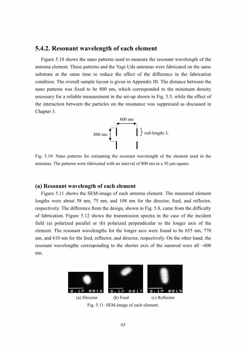
63
5.4.2. Resonant wavelength of each element
Figure 5.10 shows the nano patterns used to measure the resonant wavelength of the
antenna element. These patterns and the Yagi-Uda antennas were fabricated on the same
substrate at the same time to reduce the effect of the difference in the fabrication
condition. The overall sample layout is given in Appendix III. The distance between the
nano patterns was fixed to be 800 nm, which corresponded to the minimum density
necessary for a reliable measurement in the set-up shown in Fig. 5.5, while the effect of
the interaction between the particles on the resonance was suppressed as discussed in
Chapter 3.
Fig. 5.10: Nano patterns for estimating the resonant wavelength of the element used in the
antennas. The patterns were fabricated with an interval of 800 nm in a 50 μm square.
(a) Resonant wavelength of each element
Figure 5.11 shows the SEM-image of each antenna element. The measured element
lengths were about 58 nm, 75 nm, and 108 nm for the director, feed, and reflector,
respectively. The difference from the design, shown in Fig. 5.8, came from the difficulty
of fabrication. Figure 5.12 shows the transmission spectra in the case of the incident
field (a) polarized parallel or (b) polarized perpendicular to the longer axis of the
element. The resonant wavelengths for the longer axis were found to be 655 nm, 770
nm, and 610 nm for the feed, reflector, and director, respectively. On the other hand, the
resonant wavelengths corresponding to the shorter axis of the nanorod were all ~600
nm.
(a) Director (b) Feed (c) Reflector
Fig. 5.11: SEM-image of each element.
800 nm
800 nm
rod-length; L

64
(a)
(b)
Fig. 5.12: Transmission spectra of each element used in the antennas. (a) Incident field was
polarized parallel to the longer axis of the element. The black solid lines are the result of the
dipole model fitting based on the Eq. (5.1). (b) Incident field was polarized parallel to the
shorter axis of the element.
Ein
Ein

65
(b) Estimation of the dipole parameters
In order to compare the experimental result with the prediction based on the coupled
dipole model, parameters of each antenna element were estimated.
According to the Eq. (2.36), the polarizability α of the nanoparticle can be expressed
in terms of the volume V, the depolarization factor N, and the dielectric constant εr of
the particle material relative to the surrounding medium (εr = εp / εmed) as follows.
(5.1)
The imaginary part of α describes the extinction by the nanoparticle [37]. Therefore,
the parameters of the fabricated element can be evaluated by fitting the imaginary part
of Eq. (5.1) with the measured transmission spectra (extinction spectra) of the element.
The black solid lines in Fig. 5.12 (a) show the results of the fitting. In that case, the
surrounding medium was assumed to be SiOx (εmed ~ 2.1), and εp was given by the
literature [38]. The obtained fitting parameters are listed in Table 5.2. The validity of
this analytical approach is ensured by the fact that the fitting value of the volume was
almost the same as the designed value.
On the other hand, the material loss γ of each element was estimated by substituting
the volume V into Eq. (2.38) at the wavelength of 662 nm (vacuum). The evaluated
material losses were less than 0.5 as shown in Table 5.2. Since an antenna could show
the directional emission when the material losses were less than γ = 1.0 as predicted in
Section 4.2.5, the fabricated antennas should be capable of showing the desired
directivity. Additionally, the element detuning δ at 662 nm was estimated by substituting
the obtained N and V into Eq. (2.39).
Table 5.2: The parameters of the antenna element estimated by fitting the transmission spectra
shown in Fig. 5.12 (a) with the imaginary part of the polarizability given by Eq. (5.1). The loss
parameter γ and the element detuning δ were estimated at the wavelength of 662 nm (vacuum),
embedded in SiOx (εmed ~ 2.1).
Resonant
wavelength
[nm]
Depolarization
Factor N
Volume of nanoparticle
V [m3]
(Designed value)
Loss
parameter
γ
Element
detuning
δ
Reflector 770 0.09 2.5×10⁻²²
(3.12×10⁻²²
) 0.285 1.09
Feed 655 0.135 1.88×10⁻²²
(2.65×10⁻²²
) 0.380 -0.32
Director 610 0.173 1.63×10⁻²²
(1.88×10⁻²²
) 0.438 -2.09

66
5.4.3. Directionality
5.4.3.1. Feed element
The validity of driving method of the antenna, namely the tilting of the feed element,
described in Section 5.2 was confirmed by investigating the radiation pattern of the feed
element having neither reflector nor director.
Figure 5.13 shows a SEM image of the feed and the radiation pattern. The
polarization of the incident field Ein was tilted by 45° from the major axis of the feed,
and the polarization of the detected field Edetect was perpendicular to that of Ein. The
measured results (solid circles) were normarlized by the maximum intensity. The
radiation pattern is nearly symmetric around the normal to the surface, indicating that
the tilted feed generates the dipolar radiation with the polarization orthogonal to the
incident field. The result also indicates that the set-up is appropriate for the
measurement of directivity of the antenna emission.
On the other hand, the intensity diminishes at the angles below 20° and above 160°.
This result indicates the presence of a mismatch in the indices of refraction above and
below the feed. The open circles represent the radiation pattern of a single dipole placed
at an interface between the mediums, whose refractive index above the dipole (0°~180°)
is lower than that below the dipole, calculated by the method of reciprocity [130]. The
measured radiation pattern is similar to the prediction for the refractive index ratio of
1.05, which corresponds to the refractive index ratio of the substrate (n = 1.51) to the
SiOx layer (n = 1.44). The comparison suggests that the SiOx layer between the antenna
and the glass substrate is not affecting the radiation. To clarify the reason, it is necessary
to investigate the radiation pattern from dipoles embedded in such a multi-layer
structure.

67
Fig. 5.13: Radiation pattern of the arrayed feed element. The inset shows the SEM image of the
feed. The solid and open circles are the measured results and the prediction, respectively.
5.4.3.2. 2-element antenna
(a) Feed with a reflector
Figure 5.14 shows a SEM image and the radiation pattern of the feed-reflector
antenna. The measured results are plotted by the solid dots. The prediction based on the
coupled dipole model is plotted by the open circles. The radiation patterns were
normalized by the maximum value. In the prediction, the dipole parameters listed in
Table 5.2 were used, but the refractive index difference between the layers above and
below the antenna was not taken into account. The experimental results and the
prediction agree well with each other except in the angle region close to the interface.
The radiation in the backward direction is suppressed quite well, indicating that the
reflector works as expected. The diminishing intensity in the measured emission pattern
around 0° and 180° can be explained in terms of the difference in the refractive index
between the SiOx film and the substrate as mentioned in Section 5.4.3.1.
In particular, the angle and the depth of the dip observed around 135° in the
measured radiation pattern agree well to the prediction. In principle, the difference in
phase and intensity of the emission between the feed and the reflector decides the angle
and the depth of the dip. Therefore, it is concluded that the reflector has a desired
function as predicted in Section 4.2.2.
Edetect
Ein
100 nm
Major axis
45 °
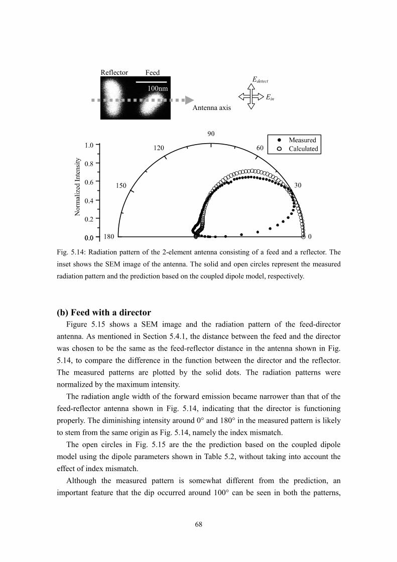
68
Fig. 5.14: Radiation pattern of the 2-element antenna consisting of a feed and a reflector. The
inset shows the SEM image of the antenna. The solid and open circles represent the measured
radiation pattern and the prediction based on the coupled dipole model, respectively.
(b) Feed with a director
Figure 5.15 shows a SEM image and the radiation pattern of the feed-director
antenna. As mentioned in Section 5.4.1, the distance between the feed and the director
was chosen to be the same as the feed-reflector distance in the antenna shown in Fig.
5.14, to compare the difference in the function between the director and the reflector.
The measured patterns are plotted by the solid dots. The radiation patterns were
normalized by the maximum intensity.
The radiation angle width of the forward emission became narrower than that of the
feed-reflector antenna shown in Fig. 5.14, indicating that the director is functioning
properly. The diminishing intensity around 0° and 180° in the measured pattern is likely
to stem from the same origin as Fig. 5.14, namely the index mismatch.
The open circles in Fig. 5.15 are the the prediction based on the coupled dipole
model using the dipole parameters shown in Table 5.2, without taking into account the
effect of index mismatch.
Although the measured pattern is somewhat different from the prediction, an
important feature that the dip occurred around 100° can be seen in both the patterns,
Edetect
Ein
100nm Reflector Feed
Antenna axis
100nm

69
showing that the director is working as expected. Possible reasons for the discrepancy
will be discussed in Section 5.4.4(b).
It is confirmed by the comparison of Fig. 5.14 with Fig. 5.15 that the element
detuning can control the function of plasmon-based antennas in optical regime.
Fig. 5.15: Radiation pattern of the 2-element antenna consisting of a feed and a director. The
inset shows the SEM image of the antenna. The solid and open circles represent the measured
radiation pattern and the prediction based on the coupled dipole model, respectively.
5.4.3.3. 5-element antenna
Figure 5.16 shows a SEM image and the emission pattern of the 5-element optical
Yagi-Uda antenna consisting of a feed, a reflector, and three directors. The experimental
results are normalized by the maximum value and plotted by the solid dots. The forward
emission is sharper than in the case of the feed-reflector antenna shown in Fig. 5.14,
while the backward emission is more suppressed than in the case of the feed-director
antenna shown in Fig. 5.15. These are the expected features of the 5-element Yagi-Uda
antenna. The result definitely demonstrates the realization of a Yagi-Uda antenna in a
visible region. The open circles show the prediction based on the coupled dipole model.
The observed emission pattern is representing well the prediction except for the angles
close to 0° and 180° where the mismatch of the refractive index between the SiOx layer
and the substrate diminishes the radiation as mentioned in Section 5.4.3.1. In particular,
Director Feed
100 nm Ein
Edetect

70
the intensity dips appear around 60° and 120° in both the experiment and the prediction,
indicating that the control of the radiation pattern is realized by the operating principles
of the Yagi-Uda antenna described in Chapter 4.
Fig. 5.16: Emission pattern from the 5-element antenna consisting of a feed, a reflector, and
three directors. The inset shows the SEM image of the antenna. The solid (●) and open circles
(○) represent the measured radiation pattern and the prediction based on the coupled dipole
model, respectively.
Reflector Director Feed
Ein
Edetect
100 nm
71
5.4.4. Discussions
(a) Effect of index mismatch on the radiation from the feed
In section 5.4.3.1, the radiation pattern of the feed, which diminishes at the angles
around 0° and 180°, was explained as the result of the index mismatch between the
medium above and below the antenna by the comparison of the measured radiation
pattern with a prediction based on the reciprocity theorem [130]. In the theory, the
emitter is assumed to be an infinitesimal dipole that oscillates parallel to the electric
field of consideration. In the experiment, however, the feed had a finite size and the
driving and detecting polarizations were orthogonal with each other and both were
rotated by 45° from the major axis of the feed. In order to investigate the effect of index
mismatch in the experimental situation, the FDTD simulation was performed with a
model shown in Fig. 5.17(a). The size and the shape of the feed was the same as those
shown in Fig.5.4. The polarization of the incident field Ein was tilted by 45° from the
major axis of the feed and the polarization direction of the detection field Edetect was
perpendicular to that of the incident field.
Figure 5.17(b) shows the experimental result and the calculated radiation pattern
from the feed element placed at the dielectric interface in the case that the refractive
index of the upper medium (0° to 180°) was lower than that of the lower medium.
First, it was confirmed that the reciprocity-based theoretical prediction (solid line)
agrees very well with the FDTD simulation (△). Then, by comparing the experimental
result with the FDTD simulation for the three cases of the index ratio, it was again
confirmed that the experimental radiation pattern is explained by the index mismatch
with the ratio of 1.05.
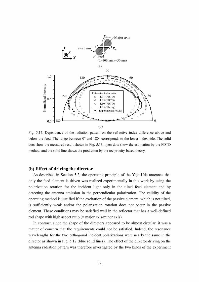
72
(a)
(b)
Fig. 5.17: Dependence of the radiation pattern on the refractive index difference above and
below the feed. The range between 0° and 180° corresponds to the lower index side. The solid
dots show the measured result shown in Fig. 5.13, open dots show the estimation by the FDTD
method, and the solid line shows the prediction by the reciprocity-based theory.
(b) Effect of driving the director
As described in Section 5.2, the operating principle of the Yagi-Uda antennas that
only the feed element is driven was realized experimentally in this work by using the
polarization rotation for the incident light only in the tilted feed element and by
detecting the antenna emission in the perpendicular polarization. The validity of the
operating method is justified if the excitation of the passive element, which is not tilted,
is sufficiently weak and/or the polarization rotation does not occur in the passive
element. These conditions may be satisfied well in the reflector that has a well-defined
rod shape with high aspect ratio (= major axis/minor axis).
In contrast, since the shape of the directors appeared to be almost circular, it was a
matter of concern that the requirements could not be satisfied. Indeed, the resonance
wavelengths for the two orthogonal incident polarizations were nearly the same in the
director as shown in Fig. 5.12 (blue solid lines). The effect of the director driving on the
antenna radiation pattern was therefore investigated by the two kinds of the experiment
Ein
Major axis Edetect
r=25 nm
Feed
(L=106 nm, t=50 nm)
Z
X
Y

73
as described below.
The first one was the evaluation of the polarization rotation in the directors, using
the nano patterns that were used to evaluate the resonant wavelength of the director in
Fig. 5.12. Since the director spacing was 800 nm as shown in Fig. 5.18, the total number
of directors in the focus spot area (15 μm by 36 μm) was about 370. Figure 5.18 shows
the radiation pattern from the directors observed in the X-Z plane. The open and solid
dots show the cases of the incident polarization parallel and perpendicular to the
detection polarization, respectively. The sharp peaks observed at 54° and 116° were
caused by the interference effect. The radiation intensity emitted to the direction of 90°
in the orthogonal driving (■) was about five times weaker than that in the parallel
driving (○), suggesting that the polarization rotation in the directors was sufficiently
small.
Additionally, the transmission spectra shown in Fig. 5.12 (a) indicate that the
response of the resonantly driven feed was stronger than the response of the directors.
Fig. 5.18: Radiation pattern of directors in the X-Z plane. The open-dots(○)/solid-dots(■) show
the cases of incident polarization parallel/perpendicular to the detection polarization.
The second experiment was performed to ensure that the directional emission of light
in the feed-director antenna shown in Fig. 5.15 was not caused by the rotation of the
Z
X
Y
Ein (■)
Edetect Ein (○)
Antenna axis
800nm
800nm
Design
Em
issi
on i
nte
nsi
ty I
(θ)/
I F
74
incident field at the directors. Figure 5.19 shows a SEM image and the radiation pattern
of the feed-director antenna in the X-Z plane. The open dots correspond to an incident
field parallel to the detected polarization (simultaneous driving of feed and director),
and the solid dots show that the incident field was polarized orthogonal to the detected
field (the results shown in Fig. 5.15). Obviously, the simultaneous driving (○) does not
result in the directional emission.
The results shown above confirm that the effect of driving directors is negligible in
the observed radiation patterns of the Yagi-Uda antennas. The results shown in Fig. 5.19
also exclude the possibility that the discrepancy between the prediction and the
experimental result for the feed-director antennas shown in Fig. 5.15 is caused by the
driving of the directors. The reason for the discrepancy is unclear. One of the
possibilities is an error of the evaluation of the director parameter from the shallow
spectral dip as shown in Fig. 5.12.
Another possibility is the proximity effect, because the tilt of the feed makes the edge
of the feed closer to the director than the center-to-center distance as described in
Section 5.2. Under these circumstances, stronger interaction than the prediction between
elements might have occurred, resulting in a higer directivity of the emission than the
prediction based on the dipole model.
Fig. 5.19: The SEM image of a feed-director antenna, and the radiation pattern of the
feed-director antennas in the X-Z plane. The open and solid dots show the cases of the incident
polarization being parallel and orthogonal to the detection polarization, respectively.
Ein (■)
Edetect
Ein (○)
Director Feed
100 nm
Antenna axis
Z
X
Y
Em
issi
on
in
ten
sity
I(θ
)/I F

75
(c) Estimation of efficiency
The radiation efficiency of the antenna was evaluated as follows. Since the input
power to the feed element depends a great deal on the alignment in the measurement
set-up, it is not appropriate to estimate the radiation efficiency from the directivity
measurement of the antennas. On the other hand, as shown in Table 5.2, the
transmission spectra could give the estimation of the material loss γ given by the
relative value to the radiation loss. Therefore, the radiation efficiency of each element is
given as 1/(1+γ). The evaluated values are listed in Table 5.3, in which γ is given by
Table 5.2. In the case of the reflector, 22.2% of the input power was lost as the material
losses, and 77.8% of the input power was emitted. In the case of the feed, 27.5% of the
input power was lost as the material losses, and 72.5% of the input power was emitted.
In the case of the directors, 30.5% of the input power was lost as the material losses,
and 69.5% of the input power was emitted.
Assuming that the interference effects in the antenna are canceled when integrating
over all radiation angles, it is possible to estimate that the radiation efficiency of the
antenna should be similar to the efficiency of the antenna elements. Therefore, the
radiation efficiency of the antenna was estimated to be at least 70 %, which was the
efficiency of the director.
Table 5.3: Ratio of the radiation and the material loss estimated at 662 nm (vacuum). The
antennas were assumed to be embedded in SiOx(n~1.44). The value of γ is given by Table 5.2.
The results shown so far suggest that the practical material loss in the gold
nanopatterns is not very large, and that the radiative interaction between antenna
elements is strong. Hence, there is a possibility that the forward radiation was further
enhanced by increasing the number of directors, as shown below. The calculation model
is the same as that shown in Fig. 4.15, except for varying the number of directors. The
design parameters of each element are given by the experimental results shown in Table
5.2. In addition, following the experimental arrangement, the feed-reflector distance was
Xr=1.7 and the director spacing Xd was Xd=2.0 for all the cases. Figure 5.20 shows the
Loss parameter γ Material Loss [%]
γ/(1+γ)
Radiation [%]
1/(1+γ)
Reflector 0.285 22.2 77.8
Feed 0.380 27.5 72.5
Director 0.438 30.5 69.5
76
dependence of the antenna emission on the number of directors. Figure 5.21 shows the
dependence of the half power beam width (HPBW), and the forward I(0)/IF and the
backward I(π)/IF radiation intensities on the number of directors. The backward
emission was suppressed the most in the case of two directors. On the other hand, the
forward emission was enhanced with the increase of the number of directors. This result
suggests that even though the material losses are not negligible in optical regime,
increasing the number of directors enhances the directivity of the optical Yagi-Uda
antenna composed of gold nanorods, as in the case of RF regime.
Fig. 5.20: The prediction of the radiation pattern for various numbers of the directors, including
the material losses. The material parameters of each element are given by Table 5.2.
Fig. 5.21: Dependence of the antenna emission on the number of directors obtained by Fig. 5.20.
Open circles show the forward emission, open triangles show the backward emission, and solid
squares show the HPBW of the forward emission, respectively.
HP
BW
[d
egre
e]
Em
issi
on
in
ten
sity
I(θ
)/I F
Number of directors used in the antenna
Em
issi
on i
nte
nsi
ty I
(θ)/
I F
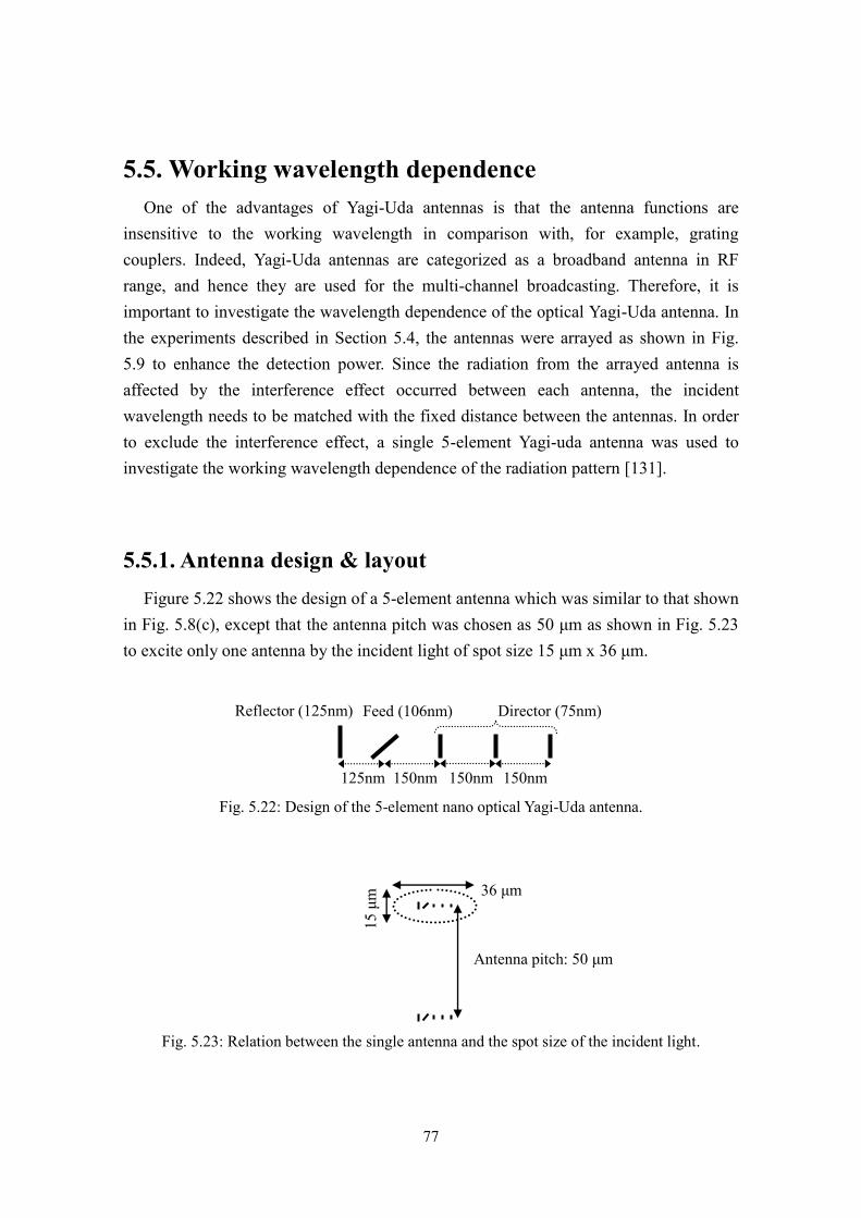
77
5.5. Working wavelength dependence
One of the advantages of Yagi-Uda antennas is that the antenna functions are
insensitive to the working wavelength in comparison with, for example, grating
couplers. Indeed, Yagi-Uda antennas are categorized as a broadband antenna in RF
range, and hence they are used for the multi-channel broadcasting. Therefore, it is
important to investigate the wavelength dependence of the optical Yagi-Uda antenna. In
the experiments described in Section 5.4, the antennas were arrayed as shown in Fig.
5.9 to enhance the detection power. Since the radiation from the arrayed antenna is
affected by the interference effect occurred between each antenna, the incident
wavelength needs to be matched with the fixed distance between the antennas. In order
to exclude the interference effect, a single 5-element Yagi-uda antenna was used to
investigate the working wavelength dependence of the radiation pattern [131].
5.5.1. Antenna design & layout
Figure 5.22 shows the design of a 5-element antenna which was similar to that shown
in Fig. 5.8(c), except that the antenna pitch was chosen as 50 μm as shown in Fig. 5.23
to excite only one antenna by the incident light of spot size 15 μm x 36 μm.
Fig. 5.22: Design of the 5-element nano optical Yagi-Uda antenna.
Fig. 5.23: Relation between the single antenna and the spot size of the incident light.
36 μm
15
μm
Antenna pitch: 50 μm
Feed (106nm) Reflector (125nm)
125nm
Director (75nm)
150nm 150nm 150nm

78
5.5.2. Resonant wavelength of each element
Figure 5.24 shows the design of nanopattern to estimate the resonant wavelength of
the antenna element. Optical antennas and nanopatterns were fabricated on the same
substrate simultaneously. The sample layout is shown in Appendix III Fig. C. Figure
5.25 shows the SEM images of the fabricated nanopatterns. The measured length of
each element was (a) 75 nm, (b) 105 nm, and (c) 121 nm. Figure 5.26 shows the
transmission spectra of the elements. The resonant wavelength corresponding to the
longer axis of the element was estimated to be 600 nm, 700 nm, and 770 nm for the
element length of 75 nm, 105 nm, and 121 nm, respectively.
Fig. 5.24: Design of nanopattern to estimate the resonant wavelength of antenna element.
(a) Director (b) Feed (c) Reflector
Fig. 5.25: SEM images of each element. Measured length (L) and width (W) were (a) L=75 nm
and W=63 nm, (b) L=105 nm and W=51 nm, (c) L=121 nm and W=53 nm.
Fig. 5.26: Transmission spectra of the element. Incident field was polarized parallel to the
longer axis of element. The black solid lines show the results of the dipole fitting. Dotted lines
with annotations show the wavelengths of laser diodes used in this work.
Pitch 800nm
Pitch 800nm
Length = 75 nm/106 nm/125 nm
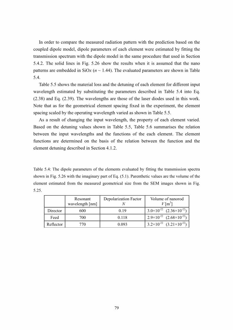
79
In order to compare the measured radiation pattern with the prediction based on the
coupled dipole model, dipole parameters of each element were estimated by fitting the
transmission spectrum with the dipole model in the same procedure that used in Section
5.4.2. The solid lines in Fig. 5.26 show the results when it is assumed that the nano
patterns are embedded in SiOx (n ~ 1.44). The evaluated parameters are shown in Table
5.4.
Table 5.5 shows the material loss and the detuning of each element for different input
wavelength estimated by substituting the parameters described in Table 5.4 into Eq.
(2.38) and Eq. (2.39). The wavelengths are those of the laser diodes used in this work.
Note that as for the geometrical element spacing fixed in the experiment, the element
spacing scaled by the operating wavelength varied as shown in Table 5.5.
As a result of changing the input wavelength, the property of each element varied.
Based on the detuning values shown in Table 5.5, Table 5.6 summarises the relation
between the input wavelengths and the functions of the each element. The element
functions are determined on the basis of the relation between the function and the
element detuning described in Section 4.1.2.
Table 5.4: The dipole parameters of the elements evaluated by fitting the transmission spectra
shown in Fig. 5.26 with the imaginary part of Eq. (5.1). Parenthetic values are the volume of the
element estimated from the measured geometrical size from the SEM images shown in Fig.
5.25.
Resonant
wavelength [nm]
Depolarization Factor
N
Volume of nanorod
V [m3]
Director 600 0.19 3.0×10⁻²²
(2.36×10⁻²²
)
Feed 700 0.118 2.9×10⁻²²
(2.68×10⁻²²
)
Reflector 770 0.093 3.2×10⁻²²
(3.21×10⁻²²
)
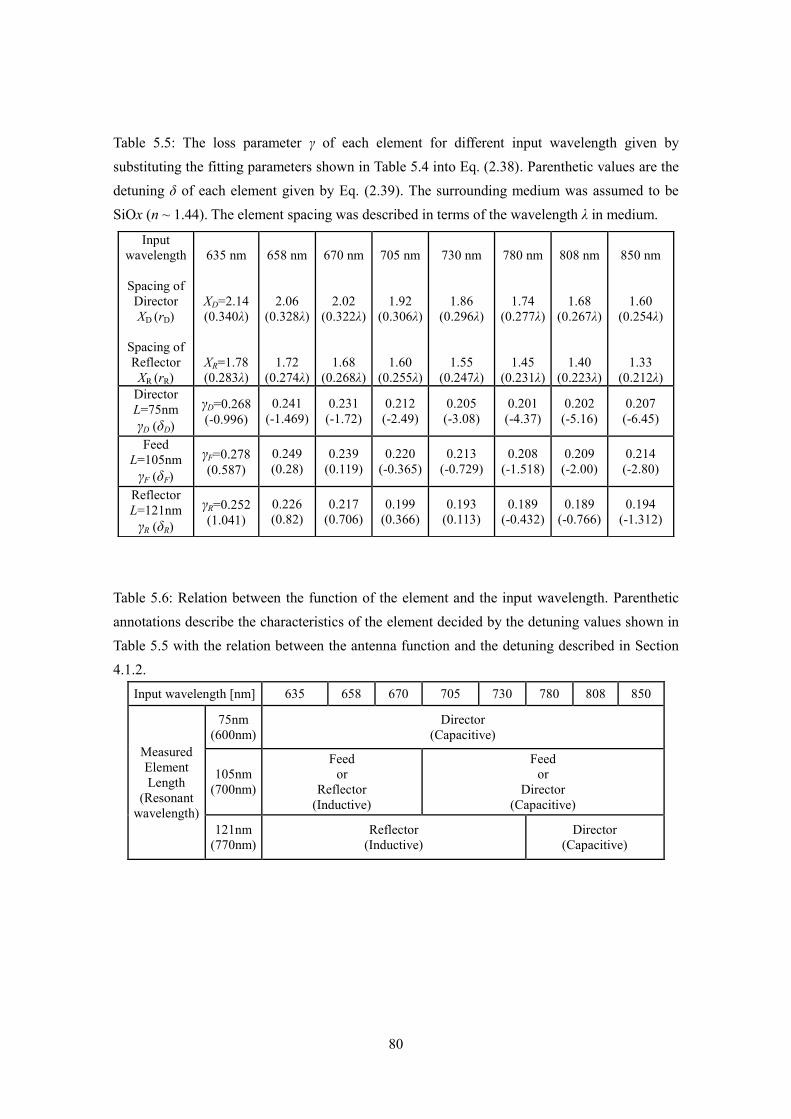
80
Table 5.5: The loss parameter γ of each element for different input wavelength given by
substituting the fitting parameters shown in Table 5.4 into Eq. (2.38). Parenthetic values are the
detuning δ of each element given by Eq. (2.39). The surrounding medium was assumed to be
SiOx (n ~ 1.44). The element spacing was described in terms of the wavelength λ in medium.
Table 5.6: Relation between the function of the element and the input wavelength. Parenthetic
annotations describe the characteristics of the element decided by the detuning values shown in
Table 5.5 with the relation between the antenna function and the detuning described in Section
4.1.2.
Input wavelength [nm] 635 658 670 705 730 780 808 850
Measured
Element
Length
(Resonant
wavelength)
75nm
(600nm)
Director
(Capacitive)
105nm
(700nm)
Feed
or
Reflector
(Inductive)
Feed
or
Director
(Capacitive)
121nm
(770nm)
Reflector
(Inductive)
Director
(Capacitive)
Input
wavelength
Spacing of
Director
XD (rD)
Spacing of
Reflector
XR (rR)
635 nm
XD=2.14
(0.340λ)
XR=1.78
(0.283λ)
658 nm
2.06
(0.328λ)
1.72
(0.274λ)
670 nm
2.02
(0.322λ)
1.68
(0.268λ)
705 nm
1.92
(0.306λ)
1.60
(0.255λ)
730 nm
1.86
(0.296λ)
1.55
(0.247λ)
780 nm
1.74
(0.277λ)
1.45
(0.231λ)
808 nm
1.68
(0.267λ)
1.40
(0.223λ)
850 nm
1.60
(0.254λ)
1.33
(0.212λ)
Director
L=75nm
γD (δD)
γD=0.268
(-0.996)
0.241
(-1.469)
0.231
(-1.72)
0.212
(-2.49)
0.205
(-3.08)
0.201
(-4.37)
0.202
(-5.16)
0.207
(-6.45)
Feed
L=105nm
γF (δF)
γF=0.278
(0.587)
0.249
(0.28)
0.239
(0.119)
0.220
(-0.365)
0.213
(-0.729)
0.208
(-1.518)
0.209
(-2.00)
0.214
(-2.80)
Reflector
L=121nm
γR (δR)
γR=0.252
(1.041)
0.226
(0.82)
0.217
(0.706)
0.199
(0.366)
0.193
(0.113)
0.189
(-0.432)
0.189
(-0.766)
0.194
(-1.312)
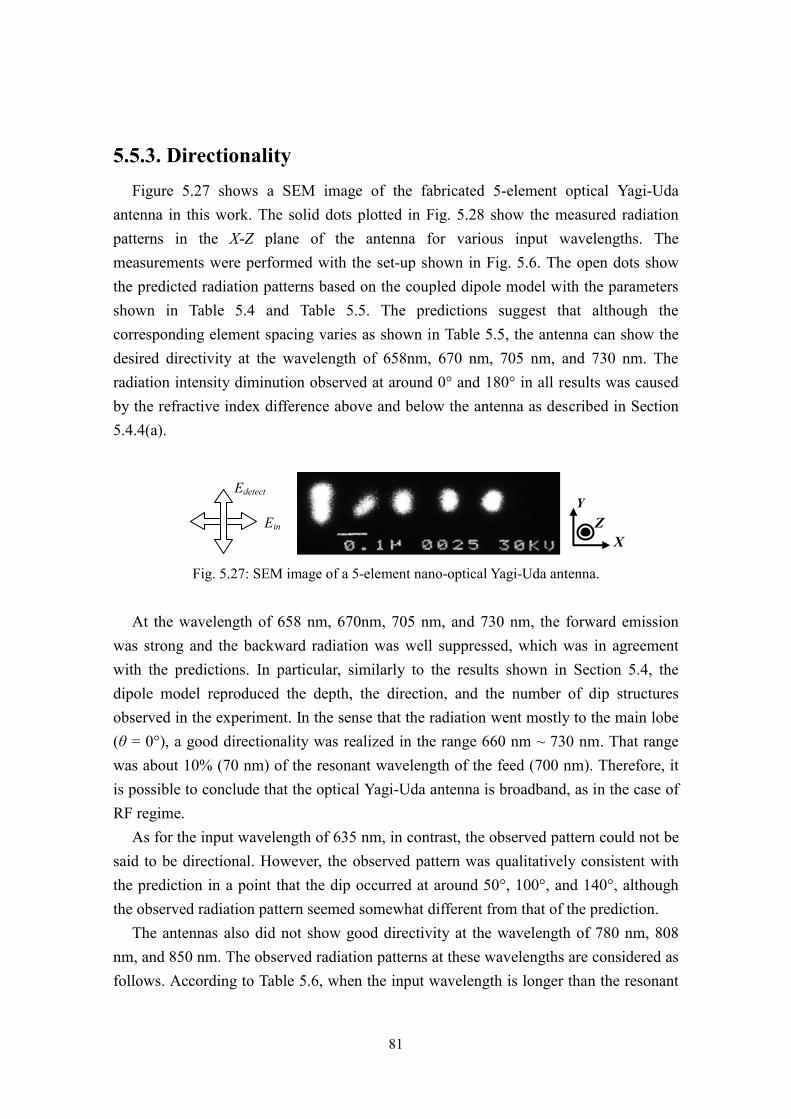
81
5.5.3. Directionality
Figure 5.27 shows a SEM image of the fabricated 5-element optical Yagi-Uda
antenna in this work. The solid dots plotted in Fig. 5.28 show the measured radiation
patterns in the X-Z plane of the antenna for various input wavelengths. The
measurements were performed with the set-up shown in Fig. 5.6. The open dots show
the predicted radiation patterns based on the coupled dipole model with the parameters
shown in Table 5.4 and Table 5.5. The predictions suggest that although the
corresponding element spacing varies as shown in Table 5.5, the antenna can show the
desired directivity at the wavelength of 658nm, 670 nm, 705 nm, and 730 nm. The
radiation intensity diminution observed at around 0° and 180° in all results was caused
by the refractive index difference above and below the antenna as described in Section
5.4.4(a).
Fig. 5.27: SEM image of a 5-element nano-optical Yagi-Uda antenna.
At the wavelength of 658 nm, 670nm, 705 nm, and 730 nm, the forward emission
was strong and the backward radiation was well suppressed, which was in agreement
with the predictions. In particular, similarly to the results shown in Section 5.4, the
dipole model reproduced the depth, the direction, and the number of dip structures
observed in the experiment. In the sense that the radiation went mostly to the main lobe
(θ = 0°), a good directionality was realized in the range 660 nm ~ 730 nm. That range
was about 10% (70 nm) of the resonant wavelength of the feed (700 nm). Therefore, it
is possible to conclude that the optical Yagi-Uda antenna is broadband, as in the case of
RF regime.
As for the input wavelength of 635 nm, in contrast, the observed pattern could not be
said to be directional. However, the observed pattern was qualitatively consistent with
the prediction in a point that the dip occurred at around 50°, 100°, and 140°, although
the observed radiation pattern seemed somewhat different from that of the prediction.
The antennas also did not show good directivity at the wavelength of 780 nm, 808
nm, and 850 nm. The observed radiation patterns at these wavelengths are considered as
follows. According to Table 5.6, when the input wavelength is longer than the resonant
Z
X
Y
Ein
Edetect

82
wavelength of the reflector (770 nm), the reflector works as director. Hence the feed is
seen as being sandwiched by the directors. It is therefore intuitively obvious that the
side lobes (radiation to the direction of 90 degrees and 270 degrees) are suppressed and
that the direction of the antenna emission is determined by the competition between the
reflector (working as a director) and the three directors. Figure 5.26 suggests that since
the response of the directors becomes weaker than that of the reflectors at such long
wavelengths, the backward emission becomes stronger than the forward emission. That
is clear in the theoretical prediction shown in Fig. 5.28.
In addition, the dipole model could not reproduce the observed radiation patterns
particularly for 808 nm and 850 nm. The reason for the discrepancy is likely to be due
to the input wavelength far from the operating range of the wavelength of the directors.
Since the emission spectrum of each nanoparticle is described by the Lorentz model, in
which the linewidth of the spectrum is finite, the parameters evaluated by the dipole
model are assumed to be different from the proper parameters when the input
wavelength is far from the resonance. In fact, as shown in Table 5.5, at the input
wavelength of 780 nm, the detuning of the director and the feed element from each
resonance wavelength were 182% (=4.37/(2(1+0.201))) and 63% (=1.518/(2(1+0.208))),
respectively of the FWHMs of the resonance.
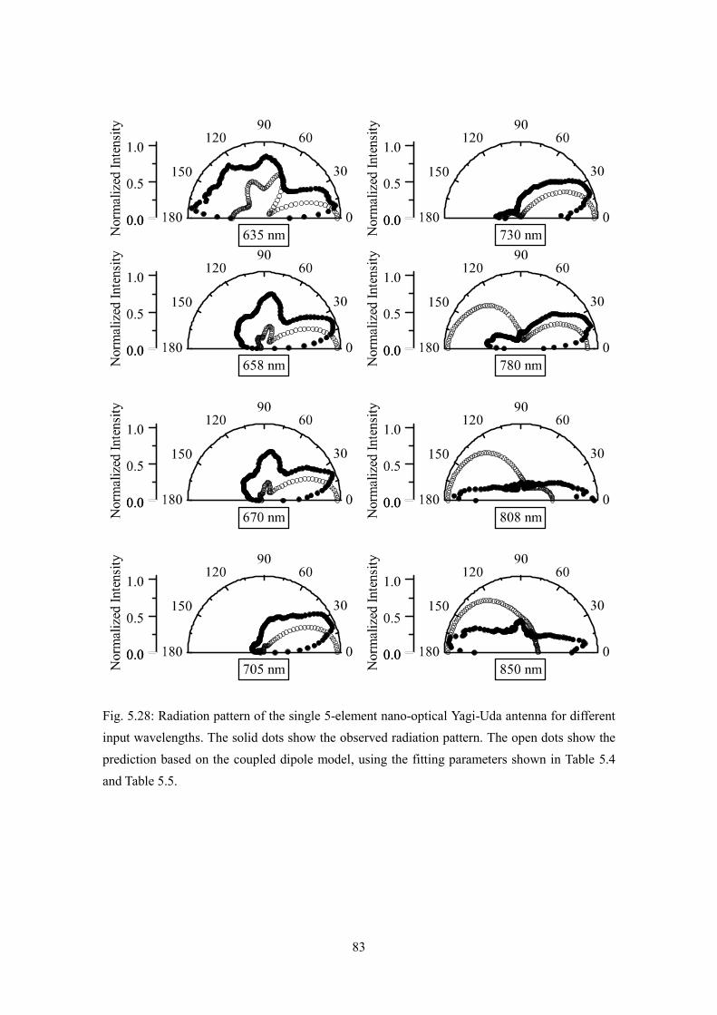
83
Fig. 5.28: Radiation pattern of the single 5-element nano-optical Yagi-Uda antenna for different
input wavelengths. The solid dots show the observed radiation pattern. The open dots show the
prediction based on the coupled dipole model, using the fitting parameters shown in Table 5.4
and Table 5.5.

84
5.6. Summary
In this chapter, experimental validation of the directional control of light with
nano-optical Yagi-Uda antennas has been described. On the basis of the antenna design
described in Chapter 4, the antennas were fabricated by the electron beam lithography
together with a bi-layer resist process and the gold lift-off process. In order to reproduce
the design assumption that the incident field should be injected only into the feed
element, the feed element was driven by the polarization dependence of the nanorod
response on the external driving field. In practice, the feed was tilted by 45 degrees
toward the antenna axis, and driven by the light poralized parallel to the antenna axis. In
order to evaluate the antenna parameters, the transmission spectra of the antenna
elements were observed and fitted with the dipole model. On the other hand, the antenna
radiation patterns were observed with a measurement system specially constructed for
this work. The findings obtained through the experiments are as follows.
a) 1-element (Feed) antenna
The radiation pattern from the arrayed feed was nearly symmetric around the
normal to the substrate. In addition, the radiation intensity was found to diminish at
the angles close to the surface of the substrate. The phenomenon was considered by
the reciprocity-based theory and the FDTD method. As a result, it was concluded that
the difference in the refractive indices between the upper layer and the lower layer of
the feed element caused the intensity diminution.
b) 2-element (Feed + Director, Feed + Reflector) antenna
A 2-element antenna consisting of a feed element and either a director or a
reflector was investigated to validate the idea that the function of the antenna element
can be controlled by adjusting the element detuning.
In the case of the feed-reflector antenna, backward radiation was suppressed very
well. Additionally, the prediction based on the coupled dipole model reproduced the
observed results very well. However, in the case of the feed-director antenna, the
observed antenna radiation pattern was somewhat different from the prediction.
Among possible reasons for the discrepancy, the possibility of the effect of
simultaneous driving of both the feed and the director elements is assuredly excluded.
As a result, the errors in the evaluation of dipole parametters of the director and the
proximity effect due to the tilting of the feed are suggested to be the reason for the
discrepancy.

85
Since the completely different patterns between the feed-reflector and the
feed-director antennas were observed, which are in agreement well with the theory, it
is concluded that the function of the element is controlled well by the element
detuning.
c) 5-element (Feed x 1, Reflector x 1, Director x 3) antenna
The radiation pattern from the 5-element antenna array was investigated. The
antenna had a reflector, a feed, and three directors. The observed pattern showed that
the forward emission was sharper, and that both the backward radiation and the side
lobes were suppressed more than those of the 2-element antenna as predicted by the
coupled dipole model. The coupled-dipole model prediction reproduced well the
observed pattern. Additionally, through the consideration of the dipole parameters
evaluated from the transmission spectrum of each element, the radiation efficiency of
the antenna was estimated to be as high as 70% with 30% material losses inside the
elements. Based on the experimental values of the dipole parametters, it is predicted
by the coupled dipole model that increasing the number of directors may enhance the
directivity of an optical Yagi-Uda antenna as in the case of RF region.
d) Dependence of the antenna radiation on the input wavelength
The dependence of the antenna radiation pattern on the input wavelength was
investigated both experimentally and theoretically by using a single 5-element
antenna. It is shown that the directional radiation is obtained in the wavelength range
of 10% of the design wavelength. It is suggested that the simple dipole model will
not be applicable to the nano rod element when the input wavelength is far from the
resonance wavelength.
86
6. Conclusion In this work, the directional control of light by a nano-optical Yagi-Uda antenna
consisting of gold nanoparticles was investigated theoretically and experimentally. On
the basis of the coupled dipole model, taking into account the material losses, the
antenna was designed and fabricated. The observed radiation pattern demonstrated the
accomplishment of realizing an optical Yagi-Uda antenna. Until this work, most of the
reports on optical antennas had focused on the single dipole antenna. In contrast, this
work demonstrated the directional control of light by arranging the dipole elements. The
results indicate that the antenna concepts and designs which are highly developled in RF
regime are applicable to the optical regime, provided that the plasmonic characteristics
of metals are appropriately taken into account. The followings are the summary of the
important findings of this work.
a) Material losses and antenna efficiency
The ohmic loss is the most significant issue in plasmonics, namely the metal-based
optical technology. It is particularly critical in localized surface plasmon (LSP) based
devices whose light field is tightly confined in the metal nanostructures. In this work, it
is clarified that the volume of the element is a key factor in lowering the effect of the
material losses, expressed by a parameter γmat (= material loss/radiation loss), and a
simple estimation method is established based on the ellipsoidal model of the particle.
By relating the γmat to the length of nanoparticles with a fixed aspect ratio 2.76 (=
major-/minor-axis) at its resonant wavelength of 705 nm (vacuum), γmat = 0.28 is found
to be achievable for the case of major-axis length 138 nm, inside glass (n=1.516). The
coupled dipole model predicts that the optical Yagi-Uda antenna can show a desired
directivity provided that the material losses in metals are the same or lower than the
radiation loss.
In this work, the dipole parameters of the fabricated antenna elements, including γmat,
were evaluated by the transmission spectrum of nanoparticles fitted by a dipole model.
The experimental results show qualitative similarity to the prediction of dipole model in
which γmat increases with the decrease of the volume of the nanoparticle. Even the
smallest volume, γmat of the fabricated director (major-axis length = 58 nm) is 0.438,
which satisfies the requirement for the directional emission predicted by the coupled
dipole model.
The straightforward derivation of the antenna emission efficiency is difficult to

87
estimate by measuring the radiation power, since the intensity of incident light
(excitation efficiency) strongly depends on the details of the set-up. Here, in this work,
the efficiency is roughly estimated by the evaluated antenna parameters. As a result, it is
shown that a one-third of the input power is lost as the material losses, and that the
remaining two-thirds are radiated.
b) Directivity of radiation
It is necessary for the directional emission of Yagi-Uda antenna to drive feed only. In
this work, the polarization dependence of the nanorod was utilized. In fact, only the feed
was tilted to 45° from the antenna axis, and the incident field was polarized parallel to
the antenna axis. By this method, it was effectively realized to drive feed only.
The directivity was measured by a homemade set-up. The feed element was
confirmed to show nearly symmetric radiation around the normal to the surface, which
validates the use of the measurement set-up as well as the driving method of the antenna
by the tilted feed. The 2-element antenna consisting of a feed and a director, and that of
a feed and a reflector showed completely different directivity with each other. That is
consistent with the prediction as well as suggests that the element’s detuning effectively
controls the element function as in RF regime. The results also suggest that even such a
simple structure can alter the directionality of emission, which will be useful for
application. The 5-element optical Yagi-Uda antenna exhibits the desired directivity as
in RF regime; the narrow forward emission is strong while the backward emission is
well suppressed.
In the measurement, diminishing emission in the vicinity of the substrate surface was
also observed. By applying the reciprocity-based theory, the results were explained by
the refractive index mismatch of ~5 % between the medium above and below the
antenna. The result suggests that the control of the refractive index surrounding the
antenna is critically important for the use of the antenna in in-plane geometry.
c) Bandwidth
The dependence of directivity of a single 5-element optical Yagi-Uda antenna on the
incident wavelength was investigated. As a result, a good directionality was obtained in
the wavelength range 660 nm ~ 730 nm. This range is about 10% of the resonant
wavelength of the feed (700 nm). Therefore, this antenna can be considered as a
broadband antenna, as in the case of RF regime.
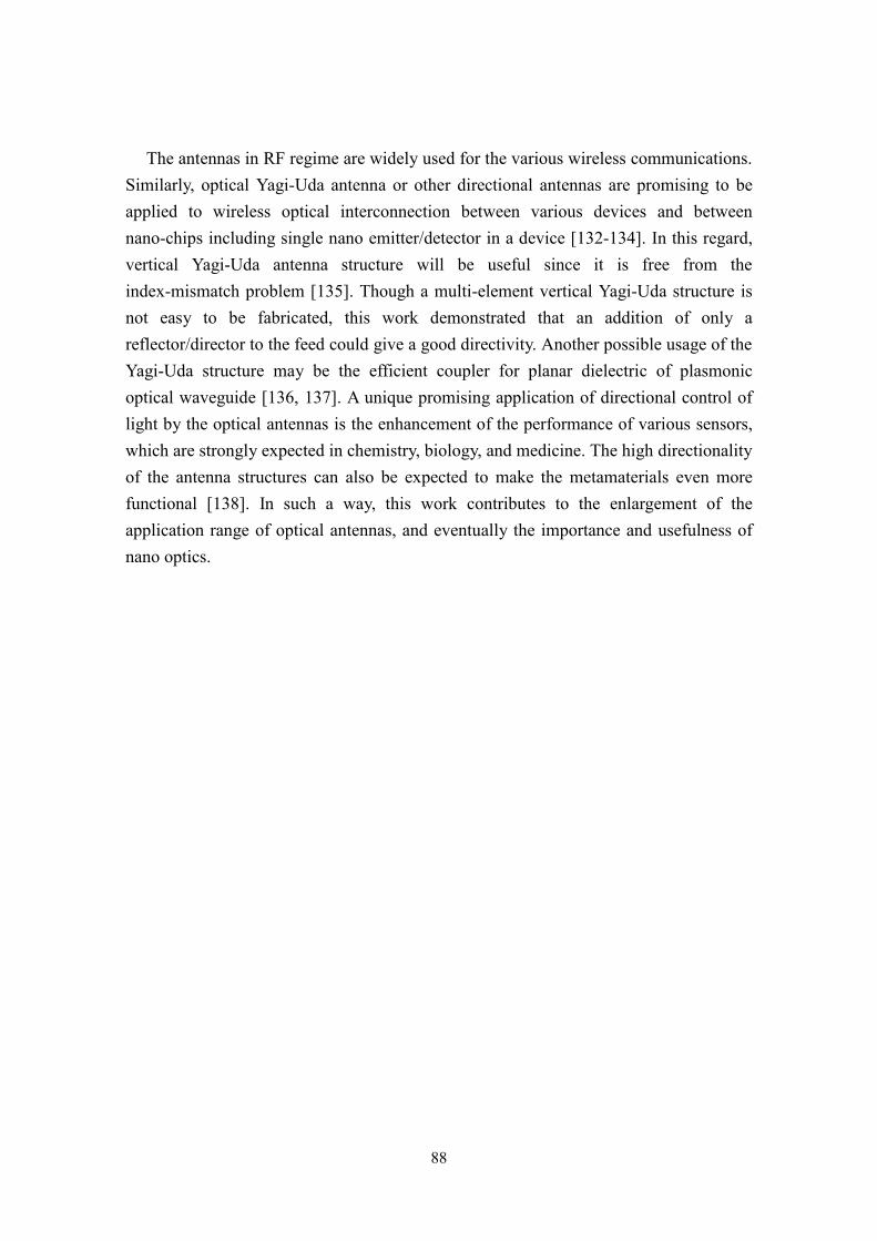
88
The antennas in RF regime are widely used for the various wireless communications.
Similarly, optical Yagi-Uda antenna or other directional antennas are promising to be
applied to wireless optical interconnection between various devices and between
nano-chips including single nano emitter/detector in a device [132-134]. In this regard,
vertical Yagi-Uda antenna structure will be useful since it is free from the
index-mismatch problem [135]. Though a multi-element vertical Yagi-Uda structure is
not easy to be fabricated, this work demonstrated that an addition of only a
reflector/director to the feed could give a good directivity. Another possible usage of the
Yagi-Uda structure may be the efficient coupler for planar dielectric of plasmonic
optical waveguide [136, 137]. A unique promising application of directional control of
light by the optical antennas is the enhancement of the performance of various sensors,
which are strongly expected in chemistry, biology, and medicine. The high directionality
of the antenna structures can also be expected to make the metamaterials even more
functional [138]. In such a way, this work contributes to the enlargement of the
application range of optical antennas, and eventually the importance and usefulness of
nano optics.

89
References
1. L. Novotny and B. Hecht. Principles of Nano-Optics: Second Edition (Cambridge
University Press, 2012).
2. 岡本隆之, 梶川浩太郎. プラズモニクス−基礎と応用. 講談社サイエンティフィク
(2010).
3. S. A. Maier. Plasmonics: Fundamentals and Applications. Springer (2007).
4. Max Born and Emi Wolf (著), 草川徹, 横田英嗣(訳): 光学の原理 I, 東海大学出版会
(1974).
5. E. Abbe. Beiträge zur Theorie des Mikroskops und der mikroskopischen Wahrnehmung.
Arch. Mikroskop. Anat., vol. 9, p. 413-420 (1873).
6. L. Rayleigh. On the theory of optical images, with special reference to the microscope.
Philos. Mag., vol. 42, p. 167-195 (1896).
7. M. Minsky. Memoir on inventing the confocal scanning microscope. Scanning Vol. 10, Iss.
4, p. 128–138 (1988).
8. 光学系の仕組みと応用. オプトロニクス社編集部編, オプトロニクス社 (2003).
9. E. H. Synge. A suggested method for extending microscopic resolution into the
ultra-microscopic region. Phil. Mag., vol. 6, p. 356–362 (1928).
10. L. Novotny. The history of near-field optics. Progress in Optics, Vol. 50, ed. E. Wolf.
Amsterdam: Elsevier, p. 137-180 (2007).
11. J. Wessel. Surface-enhanced optical microscopy. J. Opt. Soc. Am. B, vol. 2, p. 1538-1541
(1985).
12. U. Ch. Fischer and D. W. Pohl. Observation of Single-Particle Plasmons by Near-Field
Optical Microscopy. Phys. Rev. Lett. vol. 62, p.458 (1989).
13. L. Malmqvist and H. M. Hertz. Two-color trapped-particle optical microscopy. Opt. Lett.
vol. 19, Issue 12, p. 853-855 (1994).
14. Y. Inouye and S. Kawata. Near-field scanning optical microscope with a metallic probe tip.
Opt. Lett. vol. 19, Issue 3, p. 159-161 (1994).
15. S. Kawata, Y. Inouye and T. Sugiura. Near-Field Scanning Optical Microscope with a
Laser Trapped Probe. Jpn. J. Appl. Phys. vol. 33, L1725-1727 (1994).
16. D. W. Pohl, W. Denk, and M. Lanz. Optical stethoscopy: Image recording with resolution
λ/20. Appl. Phys. Lett. vol. 44, p.651 (1984).
17. A. Lewis, M. Isaacson, A. Harootunian, A. Muray. Development of a 500 Å spatial
resolution light microscope. Ultramicroscopy. Vol. 13, p. 227–231 (1984).
18. G. Binnig, H. Rohrer, Ch. Gerber, and E. Weibel. Tunneling through a controllable
vacuum gap. Appl. Phys. Lett. vol. 40, p.178 (1982).
19. R. H. Ritchie. Plasma Losses by Fast Electrons in Thin Films. Phys. Rev. vol. 106, p. 874
(1957).
20. C. J. Powell and J. B. Swan. Effect of Oxidation on the Characteristic Loss Spectra of
Aluminum and Magnesium. Phys. Rev. vol. 118, p.640 (1960).
21. A. Otto. Excitation of nonradiative surface plasma waves in silver by the method of
frustrated total reflection. Z. Phys. 216, p. 398–410 (1968).
22. E. Kretschmann and H. Räther. Radiative decay of nonradiative surface plasmon excited
by light. Z. Naturf., vol. 23A, p. 2135-2136 (1968).
23. J. Takahara, S. Yamagishi, H. Taki, A. Morimoto, and T. Kobayashi. Guiding of a
one-dimensional optical beam with nanometer diameter. Opt. Lett., Vol. 22, No. 7, p.
475-477 (1997).
24. J. Homola, Sinclair S. Yee, G. Gauglitz. Surface plasmon resonance sensors: review.

90
Sensors and Actuators B: Chemical, Vol. 54, Iss. 1–2, p. 3-15 (1999).
25. C. Nylander, B. Liedberg, T. Lind. Gas detection by means of surface plasmon resonance.
Sensors and Actuators, Vol. 3, p. 79-88 (1982/1983).
26. B. Liedberg, C. Nylander, I. Lunström. Surface plasmon resonance for gas detection and
biosensing. Sensors and Actuators, Vol. 4, p. 299-304 (1983).
27. . lavik, . Homola, . tyrok . Single-mode optical fiber surface plasmon resonance
sensor. Sensors and Actuators B: Chemical, Vol. 54, Iss. 1–2, p. 74-79 (1999).
28. . Homola, . lavík, and . tyrok . Interaction between fiber modes and surface
plasmon waves: spectral properties. Opt. Lett. vol. 22, Iss. 18, p. 1403-1405 (1997).
29. M. Mrksich, G. B. Sigal, and G. M. Whitesides. Surface Plasmon Resonance Permits in
Situ Measurement of Protein Adsorption on Self-Assembled Monolayers of
Alkanethiolates on Gold. Langmuir, vol. 11, p.4383-4385 (1995).
30. G. B. Sigal, C. Bamdad, A. Barberis, J. Strominger, and G. M. Whitesides. A
Self-Assembled Monolayer for the Binding and Study of Histidine-Tagged Proteins by
Surface Plasmon Resonance. Anal. Chem. vol. 68, p.490-497 (1996).
31. C. R. Yonzon, E. Jeoung, S. Zou, G. C. Schatz, M. Mrksich, and R. P. Van Duyne. A
Comparative Analysis of Localized and Propagating Surface Plasmon Resonance Sensors:
The Binding of Concanavalin A to a Monosaccharide Functionalized Self-Assembled Monolayer. J. AM. CHEM. SOC., vol. 126, p.12669-12676 (2004).
32. Alexandre G. Brolo. Plasmonics for future biosensors. Nat. Photon., Vol. 6, p.709-713
(2012).
33. M. Bauch, K. Toma, M. Toma, Q. Zhang, and J. Dostalek. Plasmon-Enhanced
Fluorescence Biosensors: a Review. Plasmonics 9, p.781–799 (2014).
34. C. R. Yonzon, C. L. Haynes, X. Zhang, J. T. Walsh, Jr., and R. P. Van Duyne. A Glucose
Biosensor Based on Surface-Enhanced Raman Scattering: Improved Partition Layer, Temporal Stability, Reversibility, and Resistance to Serum Protein Interference. Anal.
Chem., Vol. 76, p.78-85 (2004).
35. A. D. Taylor, J. Ladd, Q. Yu, S. Chen, J. Homola, and S. Jiang. Quantitative and
simultaneous detection of four foodborne bacterial pathogens with a multi-channel SPR
sensor. Biosensors and Bioelectronics, Vol. 22, Iss. 5, p. 752-758 (2006).
36. Gustav Mie. Contributions to the optics of turbid media, particularly of colloidal metal
solutions. Ann Phys., Vol.25, No. 3, 377-445 (1908).
37. Craig F. Bohren and Donald R. Huffman. Absorption and Scattering of Light by Small
Particles (WILEY-VCH Verlag GmbH & Co. KGaA, Weinheim, 2004).
38. P. B. Johnson and R. W. Christy. Optical Constants of the Noble Metals. Phys. Rev. B,
Vol. 6, No. 12, p. 4370-4379 (1972).
39. D. J. Barber and I. C. Freestone. An investigation of the origin of the colour of the
Lycurgus cup by analytical transmission electron microscopy. Archaeometry Vol. 32, Iss.
1, p.33-45 (1990).
40. I. Freestone, N. Meeks, M. Sax, and C. Higgitt. The Lycurgus Cup – A Roman
Nanotechnology. Gold Bulletin, 40, Iss. 4, p.270-277 (2007).
41. A. Ruivo, C. Gomes, A. Lima, M. L. Botelho, R. Melo, A. Belchior, A. P. Matos. Gold
nanoparticles in ancient and contemporary ruby glass. Journal of Cultural Heritage vol. 9,
e134-e137 (2008).
42. M. Fleischmann, P. J. Hendra, A. J. McQuillan. Raman spectra of pyridine adsorbed at a
silver electrode. Chem. Phys. Lett., vol. 26, Iss. 2, p. 163-166 (1974).
43. A. Otto, I. Mrozek, H. Grabhorn, and W. Akemann. Surface-enhanced Raman scattering. J.
Phys.: Condens. Matter, vol. 4, p.1143-1212 (1992).
44. C. V. Raman and K. S. Krishnan. A new type of secondary radiation. Nature, vol. 121, p.
501-502 (1928).
45. S. Nie and S. R. Emory. Probing Single Molecules and Single Nanoparticles by

91
Surface-Enhanced Raman Scattering. Science vol. 275, p.1102-1106 (1997).
46. H. Xu, E. J. Bjerneld, M. Käll, and L. Börjesson. Spectroscopy of Single Hemoglobin
Molecules by Surface Enhanced Raman Scattering. Phys. Rev. Lett., vol. 83, No. 21, p.
4357-4360 (1999).
47. J. Aizpurua, G. W. Bryant, L. J. Richter, and F. J. García de Abajo. Optical properties of
coupled metallic nanorods for field-enhanced spectroscopy. Phys. Rev. B. vol. 71, 235420
(2005).
48. R. Bachelot, P. Gleyzes, and A. C. Boccara. Near field optical microscopy by local
perturbation of a diffraction spot. Microsc. Microanal. Microstruct. vol. 5, p. 389-397
(1994).
49. R. Bachelot, P. Gleyzes, and A. C. Boccara. Near-field optical microscope based on local
perturbation of a diffraction spot. Opt. Lett. vol. 20, No. 18, p.1924-1926 (1995).
50. M. S. Anderson. Locally enhanced Raman spectroscopy with an atomic force microscope.
Appl. Phys. Lett. vol. 76, no. 21, p.3130-3132 (2000).
51. T. Ichimura, N. Hayazawa, M. Hashimoto, Y. Inouye, and S. Kawata. Tip-Enhanced
Coherent Anti-Stokes Raman Scattering for Vibrational Nanoimaging. Phys. Rev. Lett. vol.
92, no. 22, 220801 (2004).
52. B. Pettinger, B. Ren, G. Picardi, R. Schuster, and G. Ertl. Nanoscale Probing of Adsorbed
Species by Tip-Enhanced Raman Spectroscopy. Phys. Rev. Lett. vol. 92, no. 9, 096101
(2004).
53. C. D. Geddes, and J. R. Lakowicz. Metal-Enhanced Fluorescence. Journal of Fluorescence,
Vol. 12, No. 2, p. 121-129 (2002).
54. K. Aslan, I. Gryczynski, J. Malicka, E. Matveeva, J. R Lakowicz, and C. D. Geddes.
Metal-enhanced fluorescence: an emerging tool in biotechnology. Curr. Opin. Biotechnol.,
16, p. 55–62 (2005).
55. Y. Zhang, K. Aslan, M. J. R. Previte, and C. D. Geddes. Metal-enhanced e-type
fluorescence. Appl. Phys. Lett., Vol. 92, 013905 (2008).
56. K. Aslan, J. R Lakowicz, and C. D Geddes. Plasmon light scattering in biology and
medicine: new sensing approaches, visions and perspectives. Curr. Opin. Chem. Biol., Vol.
9, Iss. 5, p. 538–544 (2005).
57. M. D. Malinsky, K. L. Kelly, G. C. Schatz, and R. P. V. Duyne. Chain Length Dependence
and Sensing Capabilities of the Localized Surface Plasmon Resonance of Silver
Nanoparticles Chemically Modified with Alkanethiol Self-Assembled Monolayers. J. Am.
Chem. Soc., 123, p. 1471-1482 (2001).
58. P. Bharadwaj, P. Anger, and L. Novotny. Nanoplasmonic enhancement of single-molecule
fluorescence. Nanotechnology Vol. 18, 044017 (2007).
59. J. Malicka, I. Gryczynski, J. R. Lakowicz. DNA hybridization assays using
metal-enhanced fluorescence. Biochem. Biophys. Res. Commun. Vol. 306, Iss. 1, p.
213-218 (2003).
60. A. K. Sharma, R. Jha, and B. D. Gupta. Fiber-Optic Sensors Based on Surface Plasmon
Resonance: A Comprehensive Review. IEEE SENSORS JOURNAL, Vol. 7, No. 8,
p.1118-1129 (2007).
61. S. K. Srivastava, R. K. Verma, and B. D. Gupta. Theoretical modeling of a localized
surface plasmon resonance based intensity modulated fiber optic refractive index sensor.
Appl. Opt., Vol. 48, No. 19, p.3796-3802 (2009).
62. K. Mitsui, Y. Handa, and K. Kajikawa. Optical fiber affinity biosensor based on localized
surface plasmon resonance. Appl. Phys. Lett., Vol. 85, p. 4231-4233 (2004).
63. S. Pillai, K. R. Catchpole, T. Trupke, and M. A. Green. Surface plasmon enhanced silicon
solar cells. J. Appl. Phys. Vol. 101, 093105 (2007).
64. K.R. Catchpole, and A. Polman. Plasmonic solar cells. Opt. Express, Vol. 16, No. 26, p.
21793-21800 (2008).

92
65. H. A. Atwater and A. Polman. Plasmonics for improved photovoltaic devices. Nature
Materials, Vol. 9, p. 205–213 (2010).
66. P. Spinelli and A. Polman. Light Trapping in Thin Crystalline Si Solar Cells Using Surface
Mie Scatterers. IEEE J. Photovolt., Vol. 4, No. 2, p. 554-559 (2014).
67. B. Lamprecht, G. Schider, R. T. Lechner, H. Ditlbacher, J. R. Krenn, A. Leitner, and F. R.
Aussenegg. Metal Nanoparticle Gratings: Influence of Dipolar Particle Interaction on the
Plasmon Resonance. Phys. Rev. Lett., Vol. 84, No. 20, p. 4721-4724 (2000).
68. Q.-H. Wei, K.-H. Su, S. Durant, and X. Zhang. Plasmon Resonance of Finite
One-Dimensional Au Nanoparticle Chains. Nano Lett. Vol. 4, No. 6, p. 1067-1071 (2004).
69. N. Félidj, G. Laurent, J. Aubard, G. Lévi, A. Hohenau, J. R. Krenn, and F. R. Aussenegg.
Grating-induced plasmon mode in gold nanoparticle arrays. J. Chem. Phys., Vol. 123,
221103 (2005).
70. V. G. Kravets, F. Schedin, and A. N. Grigorenko. Extremely Narrow Plasmon Resonances
Based on Diffraction Coupling of Localized Plasmons in Arrays of Metallic Nanoparticles.
Phys. Rev. Lett., Vol. 101, 087403 (2008).
71. E. M. Hicks, S. Zou, G. C. Schatz, K. G. Spears, R. P. Van Duyne, L. Gunnarsson, T.
Rindzevicius, B. Kasemo, and M. Käll. Controlling Plasmon Line Shapes through
Diffractive Coupling in Linear Arrays of Cylindrical Nanoparticles Fabricated by Electron
Beam Lithography. Nano Lett., Vol. 5, No. 6, p. 1065-1070 (2005).
72. S. K. Ghosh and T. Pal. Interparticle Coupling Effect on the Surface Plasmon Resonance
of Gold Nanoparticles: From Theory to Applications. Chem. ev., Vol. 107, p. 4797−4862
(2007).
73. S. A. Maier, P. G. Kik, and H. A. Atwater. Observation of coupled plasmon-polariton
modes in Au nanoparticle chain waveguides of different lengths: Estimation of waveguide
loss. Appl. Phys. Lett., Vol. 81, No. 9, p. 1714-1716 (2002).
74. S. A. Maier, P. G. Kik, and H. A. Atwater. Optical pulse propagation in metal nanoparticle
chain waveguides. Phys. Rev. B, Vol. 67, 205402 (2003).
75. S. A. Maier, P. G. Kik, H. A. Atwater, S. Meltzer, E. Harel, B. E. Koel, and A. A. G.
Requicha. Local detection of electromagnetic energy transport below the diffraction limit
in metal nanoparticle plasmon waveguides. Nature Materials, Vol. 2, p. 229-232 (2003).
76. K. B. Crozier, E. Togan, E. Simsek, and T. Yang. Experimental measurement of the
dispersion relations of the surface plasmon modes of metal nanoparticle chains. Opt.
Express, Vol. 15, No. 26, p. 17482-17493 (2007).
77. A. F. Koenderink and A. Polman. Complex response and polariton-like dispersion splitting
in periodic metal nanoparticle chains. Phys. Rev. B, Vol. 74, 033402 (2006).
78. V. A. Markel and A. K. Sarychev. Propagation of Surface Plasmons in Ordered and
Disordered Chains of Metal Nanospheres. Phys. Rev. B, Vol. 75, 085426 (2007).
79. H. Cao. Review on latest developments in random lasers with coherent feedback. J. Phys.
A: Math. Gen. Vol. 38, p. 10497–10535 (2005).
80. C. Mateo-Segura, C. Simovski, G. Goussetis, and S. Tretyakov. Subwavelength resolution
for horizontal and vertical polarization by coupled arrays of oblate nanoellipsoids. Opt.
Lett., Vol. 34, Iss. 15, p. 2333-2335 (2009).
81. P. Alitalo, C. Simovski, A. Viitanen, and S. Tretyakov. Near-field enhancement and
subwavelength imaging in the optical region using a pair of two-dimensional arrays of
metal nanospheres. Phys. Rev. B, Vol. 74, p. 235425 (2006).
82. S. Steshenko, F. Capolino, P. Alitalo, and S. Tretyakov. Effective model and investigation
of the near-field enhancement and subwavelength imaging properties of multilayer arrays
of plasmonic nanospheres. Phys. Rev. E, Vol. 84, 016607 (2011).
83. R. Quidant, C. Girard, Jean-Claude Weeber, and A. Dereux. Tailoring the transmittance of
integrated optical waveguides with short metallic nanoparticle chains. Phys. Rev. B, Vol.
69, 085407 (2004).

93
84. W. H. Weber and G. W. Ford. Propagation of optical excitations by dipolar interactions in
metal nanoparticle chains. Phys. Rev. B Vol. 70, 125429 (2004).
85. R. Waele, A. F. Koenderink, and A. Polman. Tunable Nanoscale Localization of Energy
on Plasmon Particle Arrays. Nano. Lett., Vol. 7, No. 7, p. 2004-2008 (2007).
86. J. B. Pendry. Negative Refraction Makes a Perfect Lens. Phys. Rev. Lett., Vol. 85, No. 18,
p. 3966-3969 (2000).
87. R. A. Shelby, D. R. Smith, S. Schultz. Experimental Verification of a Negative Index of
Refraction. Science Vol. 292, p. 77-79 (2001).
88. S. Linden, C. Enkrich, M. Wegener, J. Zhou, T. Koschny, C. M. Soukoulis. Magnetic
Response of Metamaterials at 100 Terahertz. Science Vol. 306, p. 1351-1353 (2004).
89. D. R. Smith, J. B. Pendry, M. C. K. Wiltshire. Metamaterials and Negative Refractive
Index. Science Vol. 305, p. 788-792 (2004).
90. N. Fang, H. Lee, C. Sun, X. Zhang. Sub–Diffraction-Limited Optical Imaging with a
Silver Superlens. Science Vol. 308, p. 534-537 (2005).
91. V. M. Shalaev, W. Cai, U. K. Chettiar, H. K. Yuan, A. K. Sarychev, V. P. Drachev, and A.
V. Kildishev. Negative index of refraction in optical metamaterials. Opt. Lett., Vol. 30, No.
24, p.3356-3358 (2005).
92. D. W. Pohl. “Near Field Optics een as an Antenna Problem”, in Near-Field Optics:
Principles and Applications, X. Zhu and M. Ohtsu (eds.), p. 9-21, World Scientific,
Singapore (2000).
93. J. Wessel. Surface-enhanced optical microscopy. J. Opt. Soc. Am. B, Vol. 2, Iss. 9, p.
1538-1541 (1985).
94. P. Bharadwaj, B. Deutsch, and L. Novotny. Optical Antennas. Adv. Opt. Photon. Vol. 1,
Iss. 3, p. 438-483 (2009).
95. P. Mühlschlegel, H.-J. Eisler, O. J. F. Martin, B. Hecht, and D. W. Pohl. Resonant Optical
Antennas. Science Vol. 308, p. 1607-1609 (2005).
96. L. Novotny. Effective Wavelength Scaling for Optical Antennas. Phys. Rev. Lett. Vol. 98,
266802 (2007).
97. R. D. Grober, R. J. Schoelkopf, and D. E. Prober. Optical antenna: Towards a unity
efficiency near-field optical probe. Appl. Phys. Lett. Vol. 70, No. 11, p. 1354- 1356
(1997).
98. K. B. Crozier, A. Sundaramurthy, G. S. Kino, and C. F. Quate. Optical antennas:
Resonators for local field enhancement. J. Appl. Phys., Vol. 94, No. 7, p. 4632-4642
(2003).
99. D. P. Fromm, A. Sundaramurthy, P. J. Schuck, G. Kino, and W. E. Moerner.
Gap-Dependent Optical Coupling of ingle “Bowtie” Nanoantennas esonant in the
Visible. Nano. Lett., Vol. 4, No. 5, p. 957-961 (2004).
100. P. J. Schuck, D. P. Fromm, A. Sundaramurthy, G. S. Kino, and W. E. Moerner. Improving
the Mismatch between Light and Nanoscale Objects with Gold Bowtie Nanoantennas.
Phys. Rev. Lett., Vol. 94, 017402 (2005).
101. J. N. Farahani, D. W. Pohl, H.-J. Eisler, and B. Hecht. Single Quantum Dot Coupled to a
Scanning Optical Antenna: A Tunable Superemitter. Phys. Rev. Lett., Vol. 95, 017402
(2005).
102. T. Ishi, J. Fujikata, K. Makita, T. Baba, and K. Ohashi. Si Nano-Photodiode with a Surface
Plasmon Antenna. Jpn. J. Appl. Phys., Vol. 44, No. 12, L 364–L 366 (2005).
103. H. Gersen, M. F. García-Parajó, L. Novotny, J. A. Veerman, L. Kuipers, and N. F. van
Hulst. Influencing the Angular Emission of a Single Molecule. Phys. Rev. Lett., Vol. 85,
No. 25, p. 5312-5315 (2000).
104. S. Kühn, U. Håkanson, L. Rogobete, and V. Sandoghdar. Enhancement of
Single-Molecule Fluorescence Using a Gold Nanoparticle as an Optical Nanoantenna.
Phys. Rev. Lett., Vol. 97, 017402 (2006).

94
105. L. Rogobete, F. Kaminski, M. Agio, and V. Sandoghdar. Design of plasmonic
nanoantennae for enhancing spontaneous emission. Opt. Lett. Vol. 32, No. 12, 1623-1625
(2007).
106. R. M. Bakker, H. K. Yuan, Z. Liu, V. P. Drachev, A. V. Kildishev, V. M. Shalaev, R. H.
Pedersen, S. Gresillon, A. Boltasseva. Enhanced localized fluorescence in plasmonic
nanoantennae. Appl. Phys. Lett., Vol. 92, 043101(2008).
107. A Mohammadi, V Sandoghdar, and M Agio. Gold nanorods and nanospheroids for
enhancing spontaneous emission. New J. Phys. 10, 105015 (2008).
108. A. Devilez, B. Stout, and N. Bonod. Compact Metallo-Dielectric Optical Antenna for
Ultra Directional and Enhanced Radiative Emission. ACS Nano, Vol.4, No.6, 3390-3396
(2010).
109. H. G. Frey, F. Keilmann, A. Kriele, and R. Guckenberger. Enhancing the resolution of
scanning near-field optical microscopy by a metal tip grown on an aperture probe. Appl.
Phys. Lett., Vol. 81, No. 26, 5030-5032 (2002).
110. P. Anger, P. Bharadwaj, and L. Novotny. Enhancement and Quenching of
Single-Molecule Fluorescence. Phys. Rev. Lett., Vol. 96, 113002(2006).
111. O. L. Muskens, V. Giannini, J. A. Sánchez-Gil, and J. Gómez Rivas. Strong Enhancement
of the Radiative Decay Rate of Emitters by Single Plasmonic Nanoantennas. Nano Lett.,
Vol. 7, No. 9, 2871-2875 (2007).
112. R. M Bakker, V. P Drachev, Z. Liu, H. K. Yuan, R. H Pedersen, A. Boltasseva, J. Chen, J.
Irudayaraj, A. V Kildishev, and V. M Shalaev. Nanoantenna array-induced fluorescence
enhancement and reduced lifetimes. New J. Phys. 10, 125022 (2008).
113. N. Engheta. Circuits with Light at Nanoscales: Optical Nanocircuits Inspired by
Metamaterials. Science, vol. 317, no. 5845, p. 1698-1702 (2007).
114. A. Politi, M. . Cryan, . G. arity, . Yu, and . L. O’Brien. ilica-on-Silicon Waveguide
Quantum Circuits. Science, vol. 320, p. 646-649 (2008).
115. T. Gerrits, N. Thomas-Peter, J. C. Gates, A. E. Lita, B. J. Metcalf, B. Calkins, N. A.
Tomlin, A. E. Fox, A. L. Linares, J. B. Spring, N. K. Langford, R. P. Mirin, P. G. R. Smith,
I. A. Walmsley, and S. W. Nam. On-chip, photon-number-resolving,
telecommunication-band detectors for scalable photonic information processing. Phys.
Rev. A vol. 84, 060301(R) (2011).
116. N. Engheta, A. Salandrino, and A. Alù. Circuit Elements at Optical Frequencies:
Nanoinductors, Nanocapacitors, and Nanoresistors. Phys. Rev. Lett., vol. 95, 095504
(2005).
117. A. F. Koenderink, A. Alù, A. Polman. Nanophotonics: Shrinking light-based technology.
Science, vol. 348, no. 6234, p. 516-521 (2015).
118. T. H. Taminiau, R. J. Moerland, F. B. Segerink, L. Kuipers, and N. F. van Hulst. λ/4
Resonance of an Optical Monopole Antenna Probed by Single Molecule Fluorescence.
Nano. Lett., Vol. 7, No. 1, p. 28-33 (2007).
119. T. H. Taminiau, F. D. Stefani, F. B. Segerink, and N. F. Van Hulst. Optical antennas direct
single-molecule emission. Nature Photon. Vol. 2, p. 234-237 (2008).
120. C. A. Balanis. ANTENNA THEORY ANALYSYS AND DESIGN 3rd edition, p.577 (A
John Wiley & Sons, Inc., Hoboken, N.J. 2005).
121. Peter P. Viezbicke, Yagi Antenna Design. NBS TECHNICAL NOTE 688 (1976).
122. Holger F. Hofmann, Terukazu Kosako, and Yutaka Kadoya. Design parameters for a
nano-optical Yagi–Uda antenna. New J. Phys. 10, p. 217 (2007).
123. Terukazu Kosako, Yutaka Kadoya and Holger F. Hofmann. Directional control of light by
a nano-optical Yagi–Uda antenna. Nature Photon., Vol. 4, p. 312–315 (2010).
124. J. Li, A. Salandrino, and N. Engheta. Shaping light beams in the nanometer scale: A
Yagi-Uda nanoantenna in the optical domain. Phys. Rev. B, vol. 76, 245403 (2007).
125. J. Li, A. Salandrino, and N. Engheta. Optical spectrometer at the nanoscale using optical

95
Yagi-Uda nanoantennas. Phys. Rev. B, vol. 79, 195104 (2009).
126. 新井宏之, “新アンテナ工学”, 総合電子出版社 (1996).
127. J. A. Osborn. Demagnetizing Factors of the General Ellipsoid. Phys. Rev., Vol. 67, No. 11,
p. 351-357 (1945).
128. I. Maximov, E.-L. Sarwe, M. Beck, K. Deppert, M. Graczyk, M.H. Magnusson, L.
Montelius. Fabrication of Si-based nanoimprint stamps with sub-20 nm features.
Microelectronic Engineering 61–62 (2002) 449–454.
129. L. An, Y. Zheng, K. Li, P. Luo, and Y. Wu. Nanometer metal line fabrication using a
ZEP520/50 K PMMA bilayer resist by e-beam lithography. J. Vac. Sci. Technol. B vol. 23
1603 (2005).
130. D. B. Rutledge, M. S. Muha. Imaging Antenna Arrays. IEEE Trans. Antennas Propagat. ,
vol. AP-30, No. 4, p.535-540 (1982).
131. Akira Yoshida, Terukazu Kosako, Yutaka Kadoya, and Holger F. Hofmann. Radiation
pattern of a single optical Yagi-Uda antenna. The Japan Society of Applied Physics, The
71th Fall meeting, 17p-NJ-1 (in Japanese) (2010).
132. A. G. Curto, G. Volpe, T. H. Taminiau, M. P. Kreuzer, R. Quidant, and N. F. van Hulst.
Unidirectional Emission of a Quantum Dot Coupled to a Nanoantenna. Science vol. 329, p.
930 (2010).
133. Kaori Yanazawa, Yusuke Tobisu, Satoshi Maeda, Holger F. Hofmann, and Yutaka
Kadoya. Radiation and receiving gain of nano-optical Yagi-Uda antenna embedded in slab
dielectric waveguide. CLEO QF2A8, San Jose, USA (2013).
134. D. Dregely, K. Lindfors, M. Lippitz, N. Engheta, M. Totzeck, and H. Giessen. Imaging
and steering an optical wireless nanoantenna link. Nat. Commun. 5:4354 doi: 10.1038 /
ncomms 5354 (2014).
135. L. Tong, T. Pakizeh, L. Feuz, and A. Dmitriev. Highly directional bottom-up 3D
nanoantenna for visible light. Sci. Rep. 3, 2311; DOI:10.1038/srep02311 (2013).
136. D. Dregely, R. Taubert, J. Dorfmüller, R. Vogelgesang, K. Kern, and H. Giessen. 3D
optical Yagi–Uda nanoantenna array. Nat. Commun. 2:267 doi: 10.1038/ncomms1268
(2011).
137. F. B. Arango, A. Kwadrin, and A. F. Koenderink. Plasmonic Antennas Hybridized with
Dielectric Waveguides. ACS Nano, vol. 6, No. 11, p. 10156–10167 (2012).
138. N. Yu, P. Genevet, M. A. Kats, F. Aieta, Jean-Philippe Tetienne, F. Capasso, Z. Gaburro.
Light Propagation with Phase Discontinuities: Generalized Laws of Reflection and
Refraction. SCIENCE Vol. 334, p. 333 (2011).

96
Appendix I Mathematica program codes
Mathematica (Wolfram Research, Inc.) was used for the calculation of the coupled dipole
model in this work. The program codes were as follows.
* Estimation of the detuning and the material losses of antenna element by fitting the
transmission spectra of each element with dipole model (Table 5.2)
* 2-element coupled dipole model (Fig. 4.5, Fig. 4.8, Fig. 5.14, Fig. 5.15)
* 5-element coupled dipole model (Reflector x 1, Director x 3, Feed x1, Fig. 5.16, Fig. 5.28)
* Emission of dipole placed at the refractive index interface (Fig. 5.13).
* Estimating the effect of the interparticle distance on the resonant frequency/wavelength and
the line width of the emission spectra (Fig. 3.1).
*Estimation of the material-losses and the detuning value from the transmission
spectra of each element used in the antennas. Input field was polarized parallel to
the longer axis of the element. (Table 5.2)
(*Fitting Equation for the dielectric constant of the gold [38] was expressed as the following
equation . Here the unit of “ w ” is eV. *)

97
(* definition of material losses given by Eq. (2.38) *)
loss [V_, λ_, n_] :=
(* definition of detuning given by Eq. (2.39) *)
detune [V_, n_, N_, λ_] :=
(* polarizavility α given by Eq. (5.1) *)
α[ n_, V_, N_, λ_ ] :=
(* absorption coefficience for polarizavility α [37] *)
cabsorp[n_, V_, N_, λ_] :=
(* estimation for reflector *)
Import [ “l=125nm_p.txt”, “Table” ];
data1 = %;
data2 = Table
ListPlot [{data1, data2}, PlotStyle-> {Red, Blue}, FrameLabel -> {"Wavelength[nm]",
"Normalized intensity"}]
{loss[2.5*10-22
, 662, 1.44], detune[2.5*10-22
, 1.44, 0.09, 662]}
{0.284854, 1.08951}
(* estimation for feed*)
Import [ “l=106nm_p.txt”, “Table” ];
data1 = %;
data2 = Table
ListPlot [{data1, data2}, PlotStyle-> {Red, Blue}]

98
{loss[50*50*75*10-27
, 662, 1.44], detune[50*50*75*10-27
, 1.44, 0.135, 662]}
{0.379805, -0.319304}
(* estimation for director *)
Import [ “l=75nm_p.txt”, “Table” ];
data1 = %;
data2 = Table
ListPlot [{data1, data2}, PlotStyle-> {Red, Blue}]
{loss[50*50*65*10-27
, 662, 1.44], detune[50*50*65*10-27
, 1.44, 0.173, 662]}
{0.438237, -2.09497}
*2-element coupled dipole model (Fig. 4.5, Fig. 4.8, Fig. 5.14, Fig. 5.15)
xr (*reflector(or director)-feed distance*),
wr (*detuning of reflector(or director)*), mr (*material loss of reflector(or director)*),
wf (*detuning of feed*), mf (*material loss of feed*)
dipole[x_]
Solve
ar /. %;
ar[xr_, wr_, mr_, wf_, mf_] =%[[1]];

99
f[θ_, xr_, wr_, mr_, wf_, mf_] :=
Needs[“Graphics ‘Graphics’”];
(*calculation for Fig. 4.5*)
xr = -1.5
PolarPlot[f[θ, xr, -2.0, 0, 0,0], f[θ, xr, -1.0, 0, 0,0], f[θ, xr, -0.5, 0, 0,0], f[θ, xr, 0, 0, 0,0],
f[θ, xr, 0.5, 0, 0,0], f[θ, xr, 1.0, 0, 0,0], f[θ, xr, 2.0, 0, 0,0], {θ, -Pi, Pi}
(*calculation for Fig. 4.8*)
wr := 0
PolarPlot[f[θ, -1.0, wr, 0, 0,0], f[θ, -1.4, wr, 0, 0,0], f[θ, -1.8, wf, 0, 0,0], f[θ, -2.2, wf, 0, 0,0],
f[θ, -2.6, wr, 0, 0,0], f[θ, -3.0, wr, 0, 0,0] , {θ, -Pi, Pi}]
(*calculation for Fig. 5.14*)
xr := -1.708 (*position of reflector from feed, n=1.44, r=125nm, λin=662nm*)
wr := 1.0895 (*detuning of reflector*)
mr := 0.285 (*material loss of reflector*)
wf := -0.3193 (*detuning of feed*)
mf := 0.3798 (*material loss of feed*)
PolarPlot[f[θ, xr, wr, mr, wf, mf], {θ, -Pi, Pi}]
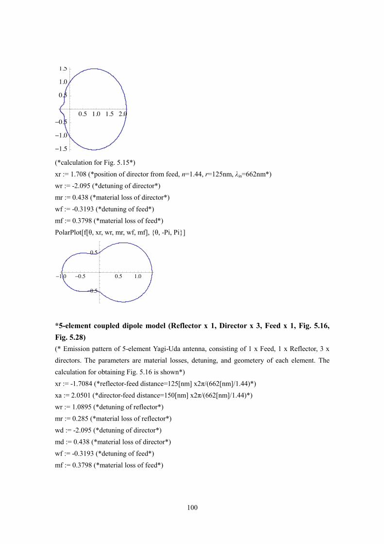
100
(*calculation for Fig. 5.15*)
xr := 1.708 (*position of director from feed, n=1.44, r=125nm, λin=662nm*)
wr := -2.095 (*detuning of director*)
mr := 0.438 (*material loss of director*)
wf := -0.3193 (*detuning of feed*)
mf := 0.3798 (*material loss of feed*)
PolarPlot[f[θ, xr, wr, mr, wf, mf], {θ, -Pi, Pi}]
*5-element coupled dipole model (Reflector x 1, Director x 3, Feed x 1, Fig. 5.16,
Fig. 5.28)
(* Emission pattern of 5-element Yagi-Uda antenna, consisting of 1 x Feed, 1 x Reflector, 3 x
directors. The parameters are material losses, detuning, and geometery of each element. The
calculation for obtaining Fig. 5.16 is shown*)
xr := -1.7084 (*reflector-feed distance=125[nm] x2π/(662[nm]/1.44)*)
xa := 2.0501 (*director-feed distance=150[nm] x2π/(662[nm]/1.44)*)
wr := 1.0895 (*detuning of reflector*)
mr := 0.285 (*material loss of reflector*)
wd := -2.095 (*detuning of director*)
md := 0.438 (*material loss of director*)
wf := -0.3193 (*detuning of feed*)
mf := 0.3798 (*material loss of feed*)
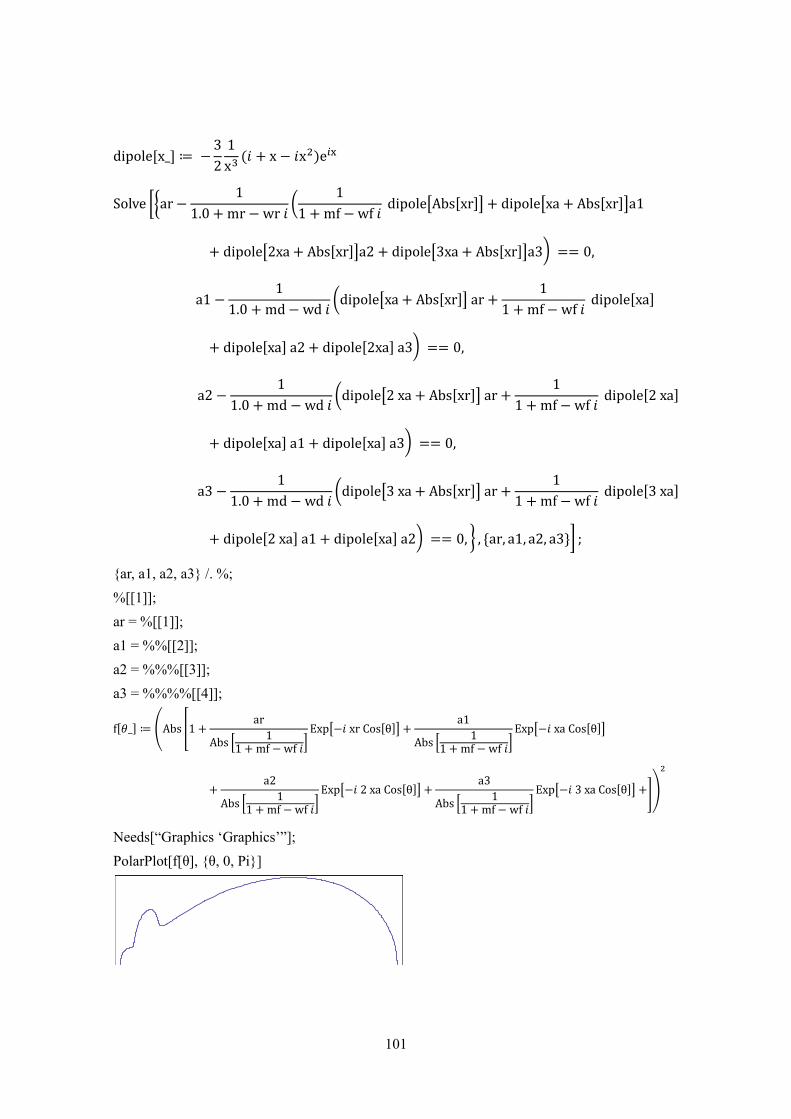
101
{ar, a1, a2, a3} /. %;
%[[1]];
ar = %[[1]];
a1 = %%[[2]];
a2 = %%%[[3]];
a3 = %%%%[[4]];
Needs[“Graphics ‘Graphics’”];
PolarPlot[f[θ], {θ, 0, Pi}]

102
*Dipole model at the index interface [130] (Fig. 5.13, Fig. 5.17)
Incident field; TE-plane, Output field; H-plane, n1; refractive index of medium, n2;
refractive index of air, and n = n1/n2.
(* H-plane, emission to the air *)
(* H-plane, emission to the dielectric *)
103
*Calculation results of FDTD for dipole emission at the index interface (Fig. 5.17)
Fig. A: Prediction based on the FDTD method in the case that only one Feed element was set at
the interface of the different index medium. The range between 0° and 180° was assumed as the
lower index medium, and the range between 180° and 360° was assumed as the higher index
medium.
*Effect of the interparticle interaction on the resonant frequency and the line
width. (Fig. 3.1)
The amount of material losses were assumed as γmat =1.0, and input field was Ein = 1.0. The
electric field amplitude of center elements was ac, all elements interacted with each other.
{ac, a1, a2} /. %;
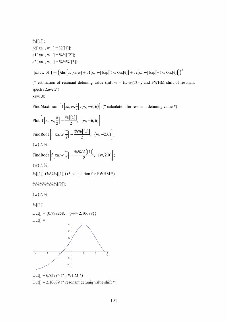
104
%[[1]];
ac[ xa_, w_ ] = %[[1]];
a1[ xa_, w_ ] = %%[[2]];
a2[ xa_, w_ ] = %%%[[3]];
(* estimation of resonant detuning value shift w = (ω-ω0)/Γ0 , and FWHM shift of resonant
spectra Δω/Γ0*)
xa=1.0;
(* calculation for resonant detuning value *)
{w} /. %;
{w} /. %;
%[[1]]-(%%%[[1]]) (* calculation for FWHM *)
%%%%%%%[[2]];
{w} /. %;
%[[1]]
Out[] = {0.798258, {w-> 2.10689}}
Out[] =
Out[] = 6.83794 (* FWHM *)
Out[] = 2.10689 (* resonant detunig value shift *)

105
Appendix II Bi-layer resist process and lift-off process
The detailed condition of sample fabrication process described in Fig. 5.1 is as follows.
①Pretreatment of glass-substrate
substrate size: 7-8 mm square
Organic solvent cleaning
1st: Acetone ultrasonic x 5min
2nd
: Trichloroethylene@~40degrees C x 5min
3rd
: Acetone ultrasonic x 5min
4th: Methanol ultrasonic x 5min
5th : Methanol ultrasonic x 5min
②1st-Spin-Coat;PMMA 950K (thickness ~50 nm)
Spin-Coat condition 1st: 500rpm x 5sec, 2
nd: 4000rpm x 60sec
Pre-Bake Hot-Plate: 180degrees C x 2min
10min Cool down
③2nd
-Spin-Coat;ZEP-520 A7 (thickness ~180 nm)
Spin-Coat condition 1st: 500rpm x 5sec, 2
nd: 7000rpm x 60sec
Pre-Bake; Hot-Plate: 180degrees C x 2min
10min Cool down
④3rd
-Spin-Coat; Conductive layer (ESPACER 300Z, thickness ~5 nm)
Spin-Coat condition 1st: 500rpm x 5sec, 2
nd: 2000rpm x 30sec
Pre-Bake; Hot-Plate: 100degrees C x 2min
10min Colld down
⑤Electron Beam Lithography
Acceleration Voltage; 30kV
Beam current: 40pA
Lithography-Mode; Line-lithograpy
Dose amount: 250-390 μC/cm2
⑥Remove conductive layer
Ultrapure water x 1min
⑦Development
ZED-N50 (n- Amylacetate)
R.T. x 40~45sec(strong agitation)
⑨1st-Rinse (Also etching the PMMA-layer )
ZMD-B (MIBK: 89%, 2-Propanol: 11%); R.T. x 90sec
⑩2nd-Rinse (Remove ZMD-B, Stop etching of PMMA-layer)
Ultrapure water; R.T. x 1min
⑪Water removal
1st: N2 -blow
⑫Resistance heating evaporation of Gold
Thickness: 50 nm, evaporation rate: 0.1 nm/sec
⑬Gold Lift-Off process
ZDMAC (n, n-Dimethylacetamide)
1st: 46-47degrees C x 3min-6min(boil)
2nd
: 46-47degrees C x 15sec-60sec Ultrasonic; gold lift-off
3rd
: 46-47degrees C x 3min-6min(boil); removal of residual resist
4th: Ultrapure water flow x 60sec; removal of organic solvent

106
Appendix III Sample layout
Fig. A: Sample layout of Fig.5.8, Fig.5.9, and Fig. 5.10 (sample No.090501C), fabricated on the
same substrate. Six different samples were fabricated on the same substrate. They consisted of
resonant wavelength detection sample for Feed, Director, and Reflector, 2-element antenna
consisting of Feed and Reflector or Feed and Director, and 5-element antenna shown in Fig. 5.8
and Fig. 5.10. In case of blocking the emission from the antenna, nothing was placed in the
X-direction, and the antenna was arrayed only to the Y-direction.
(Fig. 5.10, Fig. 5.11,
Fig. 5.12, Fig. 5.18)
Resonant wavelength
Measurement region
rod pitch; 800 nm
2-element (Fig. 5.15)
Feed (L=106 nm, 45°)
Director (L=75 nm)
Antenna pitch; 550 nm(Y-direction)
2-element (Fig. 5.14)
Feed (L=106 nm, 45°)
Reflector (L=125 nm)
Antenna pitch; 550 nm(Y-direction)
5-element (Fig. 5.16)
Feed (L=106 nm, 45°)
Reflector (L=125 nm)
Director (L=75 nm)
Antenna pitch; 550 nm(Y-direction)
L=106nm
Feed
L=125nm
Reflector
L=75nm
Director
Alignment-pattern
(50 μm x 200 μm)
500 μm
Z
X
Y
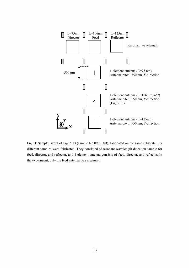
107
Fig. B: Sample layout of Fig. 5.13 (sample No.090618B), fabricated on the same substrate. Six
different samples were fabricated. They consisted of resonant wavelength detection sample for
feed, director, and reflector, and 1-element antenna consists of feed, director, and reflector. In
the experiment, only the feed antenna was measured.
L=106nm
Feed
L=125nm
Reflector
Resonant wavelength
L=75nm
Director
1-element antenna (L=75 nm)
Antenna pitch; 550 nm, Y-direction
1-element antenna (L=106 nm, 45°)
Antenna pitch; 550 nm, Y-direction
(Fig. 5.13)
1-element antenna (L=125nm)
Antenna pitch; 550 nm, Y-direction
500 μm
Z
X
Y
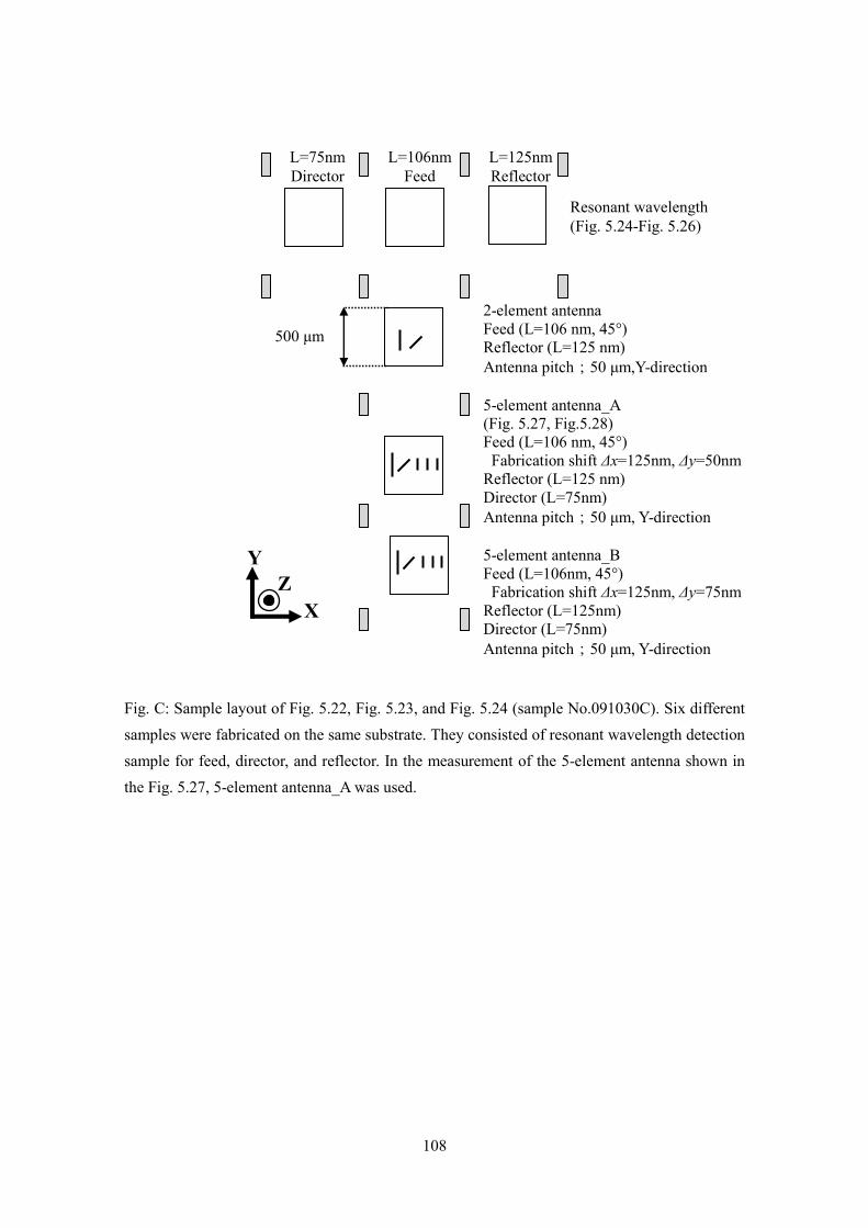
108
Fig. C: Sample layout of Fig. 5.22, Fig. 5.23, and Fig. 5.24 (sample No.091030C). Six different
samples were fabricated on the same substrate. They consisted of resonant wavelength detection
sample for feed, director, and reflector. In the measurement of the 5-element antenna shown in
the Fig. 5.27, 5-element antenna_A was used.
Resonant wavelength
(Fig. 5.24-Fig. 5.26)
2-element antenna
Feed (L=106 nm, 45°)
Reflector (L=125 nm)
Antenna pitch;50 μm,Y-direction
5-element antenna_A
(Fig. 5.27, Fig.5.28)
Feed (L=106 nm, 45°)
Fabrication shift Δx=125nm, Δy=50nm
Reflector (L=125 nm)
Director (L=75nm)
Antenna pitch;50 μm, Y-direction
5-element antenna_B
Feed (L=106nm, 45°)
Fabrication shift Δx=125nm, Δy=75nm
Reflector (L=125nm)
Director (L=75nm)
Antenna pitch;50 μm, Y-direction
L=106nm
Feed
L=125nm
Reflector
L=75nm
Director
500 μm
Z
X
Y

公表論文
(Published Papers)
(1) Design parameters for a nano-optical Yagi-Uda antenna.
Holger F Hofmann, Terukazu Kosako and Yutaka Kadoya.
New Journal of Physics, 9, 217, 1-12 (2007).
(2) Directional control of light by a nano-optical Yagi-Uda antenna.
Terukazu Kosako, Yutaka Kadoya and Holger F. Hofmann.
Nature Photonics, 4, 312-315 (2010).