Structure determination of multilayer silicene grown on Ag ...
5
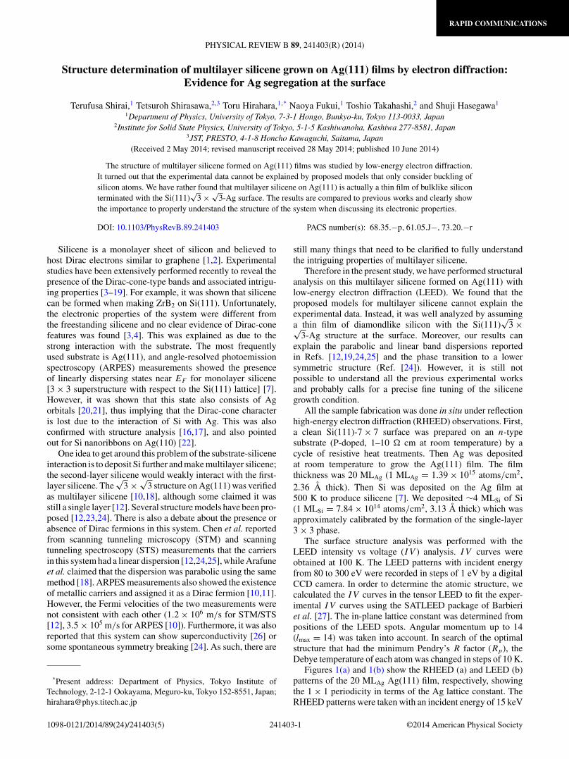
RAPID COMMUNICATIONS PHYSICAL REVIEW B 89, 241403(R) (2014) Structure determination of multilayer silicene grown on Ag(111) films by electron diffraction: Evidence for Ag segregation at the surface Terufusa Shirai, 1 Tetsuroh Shirasawa, 2, 3 Toru Hirahara, 1 , * Naoya Fukui, 1 Toshio Takahashi, 2 and Shuji Hasegawa 1 1 Department of Physics, University of Tokyo, 7-3-1 Hongo, Bunkyo-ku, Tokyo 113-0033, Japan 2 Institute for Solid State Physics, University of Tokyo, 5-1-5 Kashiwanoha, Kashiwa 277-8581, Japan 3 JST, PRESTO, 4-1-8 Honcho Kawaguchi, Saitama, Japan (Received 2 May 2014; revised manuscript received 28 May 2014; published 10 June 2014) The structure of multilayer silicene formed on Ag(111) films was studied by low-energy electron diffraction. It turned out that the experimental data cannot be explained by proposed models that only consider buckling of silicon atoms. We have rather found that multilayer silicene on Ag(111) is actually a thin film of bulklike silicon terminated with the Si(111) √ 3 × √ 3-Ag surface. The results are compared to previous works and clearly show the importance to properly understand the structure of the system when discussing its electronic properties. DOI: 10.1103/PhysRevB.89.241403 PACS number(s): 68.35.−p, 61.05.J−, 73.20.−r Silicene is a monolayer sheet of silicon and believed to host Dirac electrons similar to graphene [1,2]. Experimental studies have been extensively performed recently to reveal the presence of the Dirac-cone-type bands and associated intrigu- ing properties [3–19]. For example, it was shown that silicene can be formed when making ZrB 2 on Si(111). Unfortunately, the electronic properties of the system were different from the freestanding silicene and no clear evidence of Dirac-cone features was found [3,4]. This was explained as due to the strong interaction with the substrate. The most frequently used substrate is Ag(111), and angle-resolved photoemission spectroscopy (ARPES) measurements showed the presence of linearly dispersing states near E F for monolayer silicene [3 × 3 superstructure with respect to the Si(111) lattice] [7]. However, it was shown that this state also consists of Ag orbitals [20,21], thus implying that the Dirac-cone character is lost due to the interaction of Si with Ag. This was also confirmed with structure analysis [16,17], and also pointed out for Si nanoribbons on Ag(110) [22]. One idea to get around this problem of the substrate-silicene interaction is to deposit Si further and make multilayer silicene; the second-layer silicene would weakly interact with the first- layer silicene. The √ 3 × √ 3 structure on Ag(111) was verified as multilayer silicene [10,18], although some claimed it was still a single layer [12]. Several structure models have been pro- posed [12,23,24]. There is also a debate about the presence or absence of Dirac fermions in this system. Chen et al. reported from scanning tunneling microscopy (STM) and scanning tunneling spectroscopy (STS) measurements that the carriers in this system had a linear dispersion [12,24,25], while Arafune et al. claimed that the dispersion was parabolic using the same method [18]. ARPES measurements also showed the existence of metallic carriers and assigned it as a Dirac fermion [10,11]. However, the Fermi velocities of the two measurements were not consistent with each other (1.2 × 10 6 m/s for STM/STS [12], 3.5 × 10 5 m/s for ARPES [10]). Furthermore, it was also reported that this system can show superconductivity [26] or some spontaneous symmetry breaking [24]. As such, there are * Present address: Department of Physics, Tokyo Institute of Technology, 2-12-1 Ookayama, Meguro-ku, Tokyo 152-8551, Japan; [email protected] still many things that need to be clarified to fully understand the intriguing properties of multilayer silicene. Therefore in the present study, we have performed structural analysis on this multilayer silicene formed on Ag(111) with low-energy electron diffraction (LEED). We found that the proposed models for multilayer silicene cannot explain the experimental data. Instead, it was well analyzed by assuming a thin film of diamondlike silicon with the Si(111) √ 3 × √ 3-Ag structure at the surface. Moreover, our results can explain the parabolic and linear band dispersions reported in Refs. [12,19,24,25] and the phase transition to a lower symmetric structure (Ref. [24]). However, it is still not possible to understand all the previous experimental works and probably calls for a precise fine tuning of the silicene growth condition. All the sample fabrication was done in situ under reflection high-energy electron diffraction (RHEED) observations. First, a clean Si(111)-7 × 7 surface was prepared on an n-type substrate (P-doped, 1–10 cm at room temperature) by a cycle of resistive heat treatments. Then Ag was deposited at room temperature to grow the Ag(111) film. The film thickness was 20 ML Ag (1 ML Ag = 1.39 × 10 15 atoms/cm 2 , 2.36 ˚ A thick). Then Si was deposited on the Ag film at 500 K to produce silicene [7]. We deposited ∼4 ML Si of Si (1 ML Si = 7.84 × 10 14 atoms/cm 2 , 3.13 ˚ A thick) which was approximately calibrated by the formation of the single-layer 3 × 3 phase. The surface structure analysis was performed with the LEED intensity vs voltage (IV ) analysis. IV curves were obtained at 100 K. The LEED patterns with incident energy from 80 to 300 eV were recorded in steps of 1 eV by a digital CCD camera. In order to determine the atomic structure, we calculated the IV curves in the tensor LEED to fit the exper- imental IV curves using the SATLEED package of Barbieri et al. [27]. The in-plane lattice constant was determined from positions of the LEED spots. Angular momentum up to 14 (l max = 14) was taken into account. In search of the optimal structure that had the minimum Pendry’s R factor (R p ), the Debye temperature of each atom was changed in steps of 10 K. Figures 1(a) and 1(b) show the RHEED (a) and LEED (b) patterns of the 20 ML Ag Ag(111) film, respectively, showing the 1 × 1 periodicity in terms of the Ag lattice constant. The RHEED patterns were taken with an incident energy of 15 keV 1098-0121/2014/89(24)/241403(5) 241403-1 ©2014 American Physical Society
Transcript of Structure determination of multilayer silicene grown on Ag ...
RAPID COMMUNICATIONS
PHYSICAL REVIEW B 89, 241403(R) (2014)
Structure determination of multilayer silicene grown on Ag(111) films by electron diffraction:Evidence for Ag segregation at the surface
Terufusa Shirai,1 Tetsuroh Shirasawa,2,3 Toru Hirahara,1,* Naoya Fukui,1 Toshio Takahashi,2 and Shuji Hasegawa1
1Department of Physics, University of Tokyo, 7-3-1 Hongo, Bunkyo-ku, Tokyo 113-0033, Japan2Institute for Solid State Physics, University of Tokyo, 5-1-5 Kashiwanoha, Kashiwa 277-8581, Japan
3JST, PRESTO, 4-1-8 Honcho Kawaguchi, Saitama, Japan(Received 2 May 2014; revised manuscript received 28 May 2014; published 10 June 2014)
The structure of multilayer silicene formed on Ag(111) films was studied by low-energy electron diffraction.It turned out that the experimental data cannot be explained by proposed models that only consider buckling ofsilicon atoms. We have rather found that multilayer silicene on Ag(111) is actually a thin film of bulklike siliconterminated with the Si(111)
√3 × √
3-Ag surface. The results are compared to previous works and clearly showthe importance to properly understand the structure of the system when discussing its electronic properties.
DOI: 10.1103/PhysRevB.89.241403 PACS number(s): 68.35.−p, 61.05.J−, 73.20.−r
Silicene is a monolayer sheet of silicon and believed tohost Dirac electrons similar to graphene [1,2]. Experimentalstudies have been extensively performed recently to reveal thepresence of the Dirac-cone-type bands and associated intrigu-ing properties [3–19]. For example, it was shown that silicenecan be formed when making ZrB2 on Si(111). Unfortunately,the electronic properties of the system were different fromthe freestanding silicene and no clear evidence of Dirac-conefeatures was found [3,4]. This was explained as due to thestrong interaction with the substrate. The most frequentlyused substrate is Ag(111), and angle-resolved photoemissionspectroscopy (ARPES) measurements showed the presenceof linearly dispersing states near EF for monolayer silicene[3 × 3 superstructure with respect to the Si(111) lattice] [7].However, it was shown that this state also consists of Agorbitals [20,21], thus implying that the Dirac-cone characteris lost due to the interaction of Si with Ag. This was alsoconfirmed with structure analysis [16,17], and also pointedout for Si nanoribbons on Ag(110) [22].
One idea to get around this problem of the substrate-siliceneinteraction is to deposit Si further and make multilayer silicene;the second-layer silicene would weakly interact with the first-layer silicene. The
√3 × √
3 structure on Ag(111) was verifiedas multilayer silicene [10,18], although some claimed it wasstill a single layer [12]. Several structure models have been pro-posed [12,23,24]. There is also a debate about the presence orabsence of Dirac fermions in this system. Chen et al. reportedfrom scanning tunneling microscopy (STM) and scanningtunneling spectroscopy (STS) measurements that the carriersin this system had a linear dispersion [12,24,25], while Arafuneet al. claimed that the dispersion was parabolic using the samemethod [18]. ARPES measurements also showed the existenceof metallic carriers and assigned it as a Dirac fermion [10,11].However, the Fermi velocities of the two measurements werenot consistent with each other (1.2 × 10⁶ m/s for STM/STS[12], 3.5 × 10⁵ m/s for ARPES [10]). Furthermore, it was alsoreported that this system can show superconductivity [26] orsome spontaneous symmetry breaking [24]. As such, there are
*Present address: Department of Physics, Tokyo Institute ofTechnology, 2-12-1 Ookayama, Meguro-ku, Tokyo 152-8551, Japan;[email protected]
still many things that need to be clarified to fully understandthe intriguing properties of multilayer silicene.
Therefore in the present study, we have performed structuralanalysis on this multilayer silicene formed on Ag(111) withlow-energy electron diffraction (LEED). We found that theproposed models for multilayer silicene cannot explain theexperimental data. Instead, it was well analyzed by assuminga thin film of diamondlike silicon with the Si(111)
√3 ×√
3-Ag structure at the surface. Moreover, our results canexplain the parabolic and linear band dispersions reportedin Refs. [12,19,24,25] and the phase transition to a lowersymmetric structure (Ref. [24]). However, it is still notpossible to understand all the previous experimental worksand probably calls for a precise fine tuning of the silicenegrowth condition.
All the sample fabrication was done in situ under reflectionhigh-energy electron diffraction (RHEED) observations. First,a clean Si(111)-7 × 7 surface was prepared on an n-typesubstrate (P-doped, 1–10 � cm at room temperature) by acycle of resistive heat treatments. Then Ag was depositedat room temperature to grow the Ag(111) film. The filmthickness was 20 MLAg (1 MLAg = 1.39 × 10¹⁵ atoms/cm2,2.36 A thick). Then Si was deposited on the Ag film at500 K to produce silicene [7]. We deposited ∼4 MLSi of Si(1 MLSi = 7.84 × 10¹⁴ atoms/cm2, 3.13 A thick) which wasapproximately calibrated by the formation of the single-layer3 × 3 phase.
The surface structure analysis was performed with theLEED intensity vs voltage (IV ) analysis. IV curves wereobtained at 100 K. The LEED patterns with incident energyfrom 80 to 300 eV were recorded in steps of 1 eV by a digitalCCD camera. In order to determine the atomic structure, wecalculated the IV curves in the tensor LEED to fit the exper-imental IV curves using the SATLEED package of Barbieriet al. [27]. The in-plane lattice constant was determined frompositions of the LEED spots. Angular momentum up to 14(lmax = 14) was taken into account. In search of the optimalstructure that had the minimum Pendry’s R factor (Rp), theDebye temperature of each atom was changed in steps of 10 K.
Figures 1(a) and 1(b) show the RHEED (a) and LEED (b)patterns of the 20 MLAg Ag(111) film, respectively, showingthe 1 × 1 periodicity in terms of the Ag lattice constant. TheRHEED patterns were taken with an incident energy of 15 keV
1098-0121/2014/89(24)/241403(5) 241403-1 ©2014 American Physical Society
RAPID COMMUNICATIONS
TERUFUSA SHIRAI et al. PHYSICAL REVIEW B 89, 241403(R) (2014)
)b()a(
)d()c(
(e)
Ag 1× 1 Si 1× 1
Silicene 3 × 3Single-Layer Silicene
(f)
Silicene 3 × 3Multi-Layer Silicene
Ve 28Vek 51
a*
b*
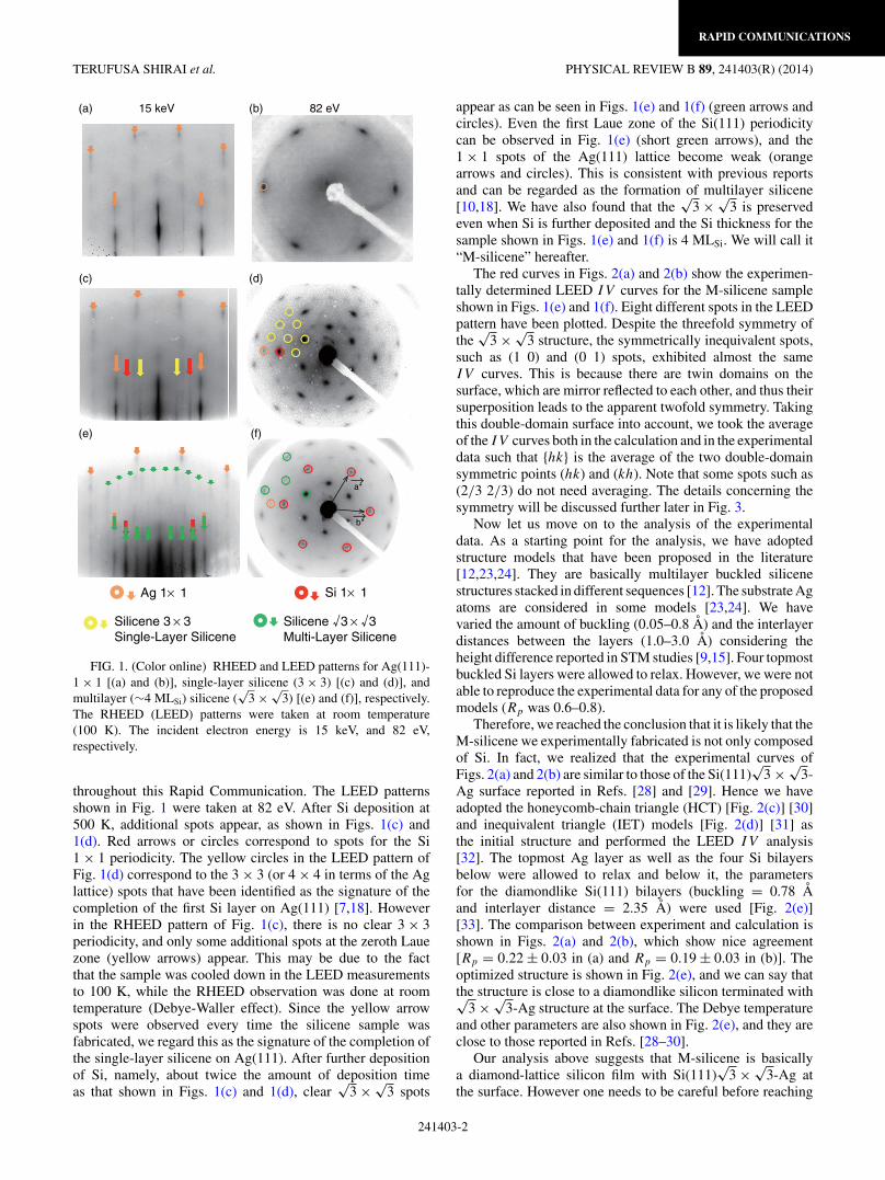
FIG. 1. (Color online) RHEED and LEED patterns for Ag(111)-1 × 1 [(a) and (b)], single-layer silicene (3 × 3) [(c) and (d)], andmultilayer (∼4 MLSi) silicene (
√3 × √
3) [(e) and (f)], respectively.The RHEED (LEED) patterns were taken at room temperature(100 K). The incident electron energy is 15 keV, and 82 eV,respectively.
throughout this Rapid Communication. The LEED patternsshown in Fig. 1 were taken at 82 eV. After Si deposition at500 K, additional spots appear, as shown in Figs. 1(c) and1(d). Red arrows or circles correspond to spots for the Si1 × 1 periodicity. The yellow circles in the LEED pattern ofFig. 1(d) correspond to the 3 × 3 (or 4 × 4 in terms of the Aglattice) spots that have been identified as the signature of thecompletion of the first Si layer on Ag(111) [7,18]. Howeverin the RHEED pattern of Fig. 1(c), there is no clear 3 × 3periodicity, and only some additional spots at the zeroth Lauezone (yellow arrows) appear. This may be due to the factthat the sample was cooled down in the LEED measurementsto 100 K, while the RHEED observation was done at roomtemperature (Debye-Waller effect). Since the yellow arrowspots were observed every time the silicene sample wasfabricated, we regard this as the signature of the completion ofthe single-layer silicene on Ag(111). After further depositionof Si, namely, about twice the amount of deposition timeas that shown in Figs. 1(c) and 1(d), clear
√3 × √
3 spots
appear as can be seen in Figs. 1(e) and 1(f) (green arrows andcircles). Even the first Laue zone of the Si(111) periodicitycan be observed in Fig. 1(e) (short green arrows), and the1 × 1 spots of the Ag(111) lattice become weak (orangearrows and circles). This is consistent with previous reportsand can be regarded as the formation of multilayer silicene[10,18]. We have also found that the
√3 × √
3 is preservedeven when Si is further deposited and the Si thickness for thesample shown in Figs. 1(e) and 1(f) is 4 MLSi. We will call it“M-silicene” hereafter.
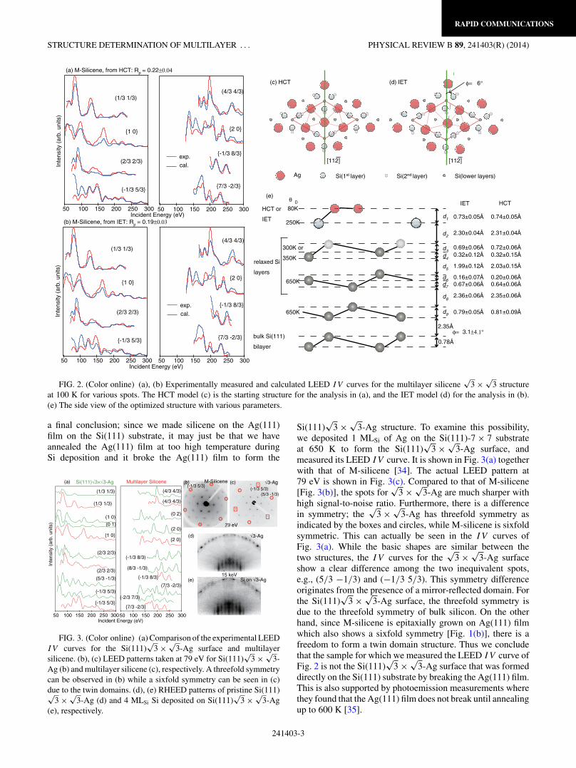
The red curves in Figs. 2(a) and 2(b) show the experimen-tally determined LEED IV curves for the M-silicene sampleshown in Figs. 1(e) and 1(f). Eight different spots in the LEEDpattern have been plotted. Despite the threefold symmetry ofthe
√3 × √
3 structure, the symmetrically inequivalent spots,such as (1 0) and (0 1) spots, exhibited almost the sameIV curves. This is because there are twin domains on thesurface, which are mirror reflected to each other, and thus theirsuperposition leads to the apparent twofold symmetry. Takingthis double-domain surface into account, we took the averageof the IV curves both in the calculation and in the experimentaldata such that {hk} is the average of the two double-domainsymmetric points (hk) and (kh). Note that some spots such as(2/3 2/3) do not need averaging. The details concerning thesymmetry will be discussed further later in Fig. 3.
Now let us move on to the analysis of the experimentaldata. As a starting point for the analysis, we have adoptedstructure models that have been proposed in the literature[12,23,24]. They are basically multilayer buckled silicenestructures stacked in different sequences [12]. The substrate Agatoms are considered in some models [23,24]. We havevaried the amount of buckling (0.05–0.8 A) and the interlayerdistances between the layers (1.0–3.0 A) considering theheight difference reported in STM studies [9,15]. Four topmostbuckled Si layers were allowed to relax. However, we were notable to reproduce the experimental data for any of the proposedmodels (Rp was 0.6–0.8).
Therefore, we reached the conclusion that it is likely that theM-silicene we experimentally fabricated is not only composedof Si. In fact, we realized that the experimental curves ofFigs. 2(a) and 2(b) are similar to those of the Si(111)
√3 × √
3-Ag surface reported in Refs. [28] and [29]. Hence we haveadopted the honeycomb-chain triangle (HCT) [Fig. 2(c)] [30]and inequivalent triangle (IET) models [Fig. 2(d)] [31] asthe initial structure and performed the LEED IV analysis[32]. The topmost Ag layer as well as the four Si bilayersbelow were allowed to relax and below it, the parametersfor the diamondlike Si(111) bilayers (buckling = 0.78 Aand interlayer distance = 2.35 A) were used [Fig. 2(e)][33]. The comparison between experiment and calculation isshown in Figs. 2(a) and 2(b), which show nice agreement[Rp = 0.22 ± 0.03 in (a) and Rp = 0.19 ± 0.03 in (b)]. Theoptimized structure is shown in Fig. 2(e), and we can say thatthe structure is close to a diamondlike silicon terminated with√
3 × √3-Ag structure at the surface. The Debye temperature
and other parameters are also shown in Fig. 2(e), and they areclose to those reported in Refs. [28–30].
Our analysis above suggests that M-silicene is basicallya diamond-lattice silicon film with Si(111)
√3 × √
3-Ag atthe surface. However one needs to be careful before reaching
241403-2
RAPID COMMUNICATIONS
STRUCTURE DETERMINATION OF MULTILAYER . . . PHYSICAL REVIEW B 89, 241403(R) (2014)
Ag Si(1st layer) Si(2nd layer) Si(lower layers)
φ= 6°TEI )d(TCH )c(
[112] [112]
d1
d2
d3d4
d5
d6d7
d8
d9
bulk Si(111)
bilayer
HCT or
IET
(e)
relaxed Si
layers
2.35Å
(1/3 1/3)
{1 0}
(2/3 2/3)
{-1/3 5/3}
50 100 150 200 250 300
(4/3 4/3)
{2 0}
{-1/3 8/3}
{7/3 -2/3}
50 100 150 200 250 300
(4/3 4/3)
{2 0}
{-1/3 8/3}
{7/3 -2/3}
50 100 150 200 250 300
(1/3 1/3)
{1 0}
(2/3 2/3)
{-1/3 5/3}
50 100 150 200 250 300
(a) M-Silicene, from HCT: Rp = 0.22±0.04
(b) M-Silicene, from IET: Rp = 0.19±0.03
Inte
nsity
(ar
b. u
nits
)In
tens
ity (
arb.
uni
ts)
Incident Energy (eV)
Incident Energy (eV)
cal.
exp.
cal.
exp.
0.73±0.05Å 0.74±0.05Å
IET HCT
2.30±0.04Å 2.31±0.04Å
0.69±0.06Å 0.72±0.06Å0.32±0.12Å 0.32±0.15Å
1.99±0.12Å 2.03±0.15Å
0.16±0.07Å 0.20±0.06Å0.67±0.06Å 0.64±0.06Å
2.36±0.06Å 2.35±0.06Å
0.79±0.05Å 0.81±0.09Å
80K
250K
300K or
350K
650K
650K
θ D
φ= 3.1±4.1°
0.78Å
FIG. 2. (Color online) (a), (b) Experimentally measured and calculated LEED IV curves for the multilayer silicene√
3 × √3 structure
at 100 K for various spots. The HCT model (c) is the starting structure for the analysis in (a), and the IET model (d) for the analysis in (b).(e) The side view of the optimized structure with various parameters.
a final conclusion; since we made silicene on the Ag(111)film on the Si(111) substrate, it may just be that we haveannealed the Ag(111) film at too high temperature duringSi deposition and it broke the Ag(111) film to form the
15 keV
(d)
(e)
√3-Ag
Si on √3-Ag
(a) Si(111)√3×√3-Ag Multilayer Silicene
30025020015010050 30025020015010050Incident Energy (eV)
(1/3 1/3)
{1 0}
(2/3 2/3)
{-1/3 5/3}
(4/3 4/3)
{2 0}
{-1/3 8/3}
{7/3 -2/3}
(2/3 2/3)
(1/3 1/3)
(2 0)
(0 2)
(4/3 4/3)
(1 0)
(0 1)
(-1/3 5/3)
(5/3 -1/3)(7/3 -2/3)
(-2/3 7/3)
(-1/3 8/3)
(8/3 -1/3)
(c) √3-Ag(-1/3 5/3)
(5/3 -1/3)
(b) M-Silicene{-1/3 5/3}
79 eV
Inte
nsity
(ar
b. u
nits
)
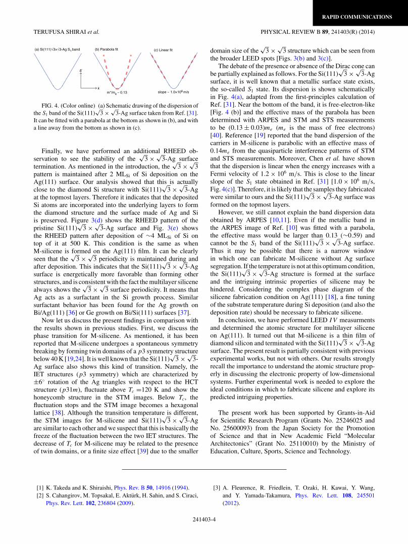
FIG. 3. (Color online) (a) Comparison of the experimental LEEDIV curves for the Si(111)
√3 × √
3-Ag surface and multilayersilicene. (b), (c) LEED patterns taken at 79 eV for Si(111)
√3 × √
3-Ag (b) and multilayer silicene (c), respectively. A threefold symmetrycan be observed in (b) while a sixfold symmetry can be seen in (c)due to the twin domains. (d), (e) RHEED patterns of pristine Si(111)√
3 × √3-Ag (d) and 4 MLSi Si deposited on Si(111)
√3 × √
3-Ag(e), respectively.
Si(111)√
3 × √3-Ag structure. To examine this possibility,
we deposited 1 MLSi of Ag on the Si(111)-7 × 7 substrateat 650 K to form the Si(111)
√3 × √
3-Ag surface, andmeasured its LEED IV curve. It is shown in Fig. 3(a) togetherwith that of M-silicene [34]. The actual LEED pattern at79 eV is shown in Fig. 3(c). Compared to that of M-silicene[Fig. 3(b)], the spots for
√3 × √
3-Ag are much sharper withhigh signal-to-noise ratio. Furthermore, there is a differencein symmetry; the
√3 × √
3-Ag has threefold symmetry asindicated by the boxes and circles, while M-silicene is sixfoldsymmetric. This can actually be seen in the IV curves ofFig. 3(a). While the basic shapes are similar between thetwo structures, the IV curves for the
√3 × √
3-Ag surfaceshow a clear difference among the two inequivalent spots,e.g., (5/3 −1/3) and (−1/3 5/3). This symmetry differenceoriginates from the presence of a mirror-reflected domain. Forthe Si(111)
√3 × √
3-Ag surface, the threefold symmetry isdue to the threefold symmetry of bulk silicon. On the otherhand, since M-silicene is epitaxially grown on Ag(111) filmwhich also shows a sixfold symmetry [Fig. 1(b)], there is afreedom to form a twin domain structure. Thus we concludethat the sample for which we measured the LEED IV curve ofFig. 2 is not the Si(111)
√3 × √
3-Ag surface that was formeddirectly on the Si(111) substrate by breaking the Ag(111) film.This is also supported by photoemission measurements wherethey found that the Ag(111) film does not break until annealingup to 600 K [35].
241403-3
RAPID COMMUNICATIONS
TERUFUSA SHIRAI et al. PHYSICAL REVIEW B 89, 241403(R) (2014)
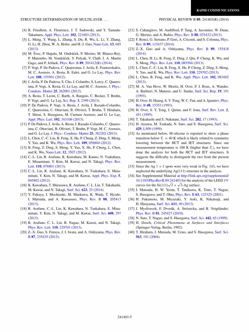
(a) Si(111)√3×√3-Ag S1 band (b) Parabola fit (c) Linear fit
k
E
m*/me ~ 0.13 slope ~ 1.0×10⁶ m/s
FIG. 4. (Color online) (a) Schematic drawing of the dispersion ofthe S1 band of the Si(111)
√3 × √
3-Ag surface taken from Ref. [31].It can be fitted with a parabola at the bottom as shown in (b), and witha line away from the bottom as shown in (c).
Finally, we have performed an additional RHEED ob-servation to see the stability of the
√3 × √
3-Ag surfacetermination. As mentioned in the introduction, the
√3 × √
3pattern is maintained after 2 MLSi of Si deposition on theAg(111) surface. Our analysis showed that this is actuallyclose to the diamond Si structure with Si(111)
√3 × √
3-Agat the topmost layers. Therefore it indicates that the depositedSi atoms are incorporated into the underlying layers to formthe diamond structure and the surface made of Ag and Siis preserved. Figure 3(d) shows the RHEED pattern of thepristine Si(111)
√3 × √
3-Ag surface and Fig. 3(e) showsthe RHEED pattern after deposition of ∼4 MLSi of Si ontop of it at 500 K. This condition is the same as whenM-silicene is formed on the Ag(111) film. It can be clearlyseen that the
√3 × √
3 periodicity is maintained during andafter deposition. This indicates that the Si(111)
√3 × √
3-Agsurface is energetically more favorable than forming otherstructures, and is consistent with the fact the multilayer silicenealways shows the
√3 × √
3 surface periodicity. It means thatAg acts as a surfactant in the Si growth process. Similarsurfactant behavior has been found for the Ag growth onBi/Ag(111) [36] or Ge growth on Bi/Si(111) surfaces [37].
Now let us discuss the present findings in comparison withthe results shown in previous studies. First, we discuss thephase transition for M-silicene. As mentioned, it has beenreported that M-silicene undergoes a spontaneous symmetrybreaking by forming twin domains of a p3 symmetry structurebelow 40 K [19,24]. It is well known that the Si(111)
√3 × √
3-Ag surface also shows this kind of transition. Namely, theIET structures (p3 symmetry) which are characterized by±6◦ rotation of the Ag triangles with respect to the HCTstructure (p31m), fluctuate above Tc =120 K and show thehoneycomb structure in the STM images. Below Tc, thefluctuation stops and the STM image becomes a hexagonallattice [38]. Although the transition temperature is different,the STM images for M-silicene and Si(111)
√3 × √
3-Agare similar to each other and we suspect that this is basically thefreeze of the fluctuation between the two IET structures. Thedecrease of Tc for M-silicene may be related to the presenceof twin domains, or a finite size effect [39] due to the smaller
domain size of the√
3 × √3 structure which can be seen from
the broader LEED spots [Figs. 3(b) and 3(c)].The debate of the presence or absence of the Dirac cone can
be partially explained as follows. For the Si(111)√
3 × √3-Ag
surface, it is well known that a metallic surface state exists,the so-called S1 state. Its dispersion is shown schematicallyin Fig. 4(a), adapted from the first-principles calculation ofRef. [31]. Near the bottom of the band, it is free-electron-like[Fig. 4 (b)] and the effective mass of the parabola has beendetermined with ARPES and STM and STS measurementsto be (0.13 ± 0.03)me (me is the mass of free electrons)[40]. Reference [19] reported that the band dispersion of thecarriers in M-silicene is parabolic with an effective mass of0.14me from the quasiparticle interference patterns of STMand STS measurements. Moreover, Chen et al. have shownthat the dispersion is linear when the energy increases with aFermi velocity of 1.2 × 10⁶ m/s. This is close to the linearslope of the S1 state obtained in Ref. [31] [1.0 × 10⁶ m/s,Fig. 4(c)]. Therefore, it is likely that the samples they fabricatedwere similar to ours and the Si(111)
√3 × √
3-Ag surface wasformed on the topmost layers.
However, we still cannot explain the band dispersion dataobtained by ARPES [10,11]. Even if the metallic band inthe ARPES image of Ref. [10] was fitted with a parabola,the effective mass would be larger than 0.13 (∼0.59) andcannot be the S1 band of the Si(111)
√3 × √
3-Ag surface.Thus it may be possible that there is a narrow windowin which one can fabricate M-silicene without Ag surfacesegregation. If the temperature is not at this optimum condition,the Si(111)
√3 × √
3-Ag structure is formed at the surfaceand the intriguing intrinsic properties of silicene may behindered. Considering the complex phase diagram of thesilicene fabrication condition on Ag(111) [18], a fine tuningof the substrate temperature during Si deposition (and also thedeposition rate) should be necessary to fabricate silicene.
In conclusion, we have performed LEED IV measurmentsand determined the atomic structure for multilayer siliceneon Ag(111). It turned out that M-silicene is a thin film ofdiamond silicon and terminated with the Si(111)
√3 × √
3-Agsurface. The present result is partially consistent with previousexperimental works, but not with others. Our results stronglyrecall the importance to understand the atomic structure prop-erly in discussing the electronic property of low-dimensionalsystems. Further experimental work is needed to explore theideal conditions in which to fabricate silicene and explore itspredicted intriguing properties.
The present work has been supported by Grants-in-Aidfor Scientific Research Program (Grants No. 25246025 andNo. 25600093) from the Japan Society for the Promotionof Science and that in New Academic Field “MolecularArchitectonics” (Grant No. 25110010) by the Ministry ofEducation, Culture, Sports, Science and Technology.
[1] K. Takeda and K. Shiraishi, Phys. Rev. B 50, 14916 (1994).[2] S. Cahangirov, M. Topsakal, E. Akturk, H. Sahin, and S. Ciraci,
Phys. Rev. Lett. 102, 236804 (2009).
[3] A. Fleurence, R. Friedlein, T. Ozaki, H. Kawai, Y. Wang,and Y. Yamada-Takamura, Phys. Rev. Lett. 108, 245501(2012).
241403-4
RAPID COMMUNICATIONS
STRUCTURE DETERMINATION OF MULTILAYER . . . PHYSICAL REVIEW B 89, 241403(R) (2014)
[4] R. Friedlein, A. Fleurence, J. T. Sadowski, and Y. Yamada-Takamura, Appl. Phys. Lett. 102, 221603 (2013).
[5] L. Meng, Y. Wang, L. Zhang, S. Du, R. Wu, L. Li, Y. Zhang,G. Li, H. Zhou, W. A. Hofer, and H.-J. Gao, Nano Lett. 13, 685(2013).
[6] M. Svec, P. Hapala, M. Ondracek, P. Merino, M. Blanco-Rey,P. Mutombo, M. Vondracek, Y. Polyak, V. Chab, J. A. MartınGago, and P. Jelınek, Phys. Rev. B 89, 201412(R) (2014).
[7] P. Vogt, P. De Padova, C. Quaresima, J. Avila, E. Frantzeskakis,M. C. Asensio, A. Resta, B. Ealet, and G. Le Lay, Phys. Rev.Lett. 108, 155501 (2012).
[8] J. Avila, P. De Padova, S. Cho, I. Colambo, S. Lorcy, C. Quares-ima, P. Vogt, A. Resta, G. Le Lay, and M. C. Asensio, J. Phys.:Condens. Matter 25, 262001 (2013).
[9] A. Resta, T. Leoni, C. Barth, A. Ranguis, C. Becker, T. Bruhn,P. Vogt, and G. Le Lay, Sci. Rep. 3, 2399 (2013).
[10] P. De Padova, P. Vogt, A. Resta, J. Avila, I. Razado-Colambo,C. Quaresima, C. Ottaviani, B. Olivieri, T. Bruhn, T. Hirahara,T. Shirai, S. Hasegawa, M. Carmen Asensio, and G. Le Lay,Appl. Phys. Lett. 102, 163106 (2013).
[11] P. De Padova, J. Avila, A. Resta, I. Razado-Colambo, C. Quares-ima, C. Ottaviani, B. Olivieri, T. Bruhn, P. Vogt, M. C. Asensio,and G. Le Lay, J. Phys.: Condens. Matter 25, 382202 (2013).
[12] L. Chen, C.-C. Liu, B. Feng, X. He, P. Cheng, Z. Ding, S. Meng,Y. Yao, and K. Wu, Phys. Rev. Lett. 109, 056804 (2012).
[13] B. Feng, Z. Ding, S. Meng, Y. Yao, X. He, P. Cheng, L. Chen,and K. Wu, Nano Lett. 12, 3507 (2012).
[14] C.-L. Lin, R. Arafune, K. Kawahara, M. Kanno, N. Tsukahara,E. Minamitani, Y. Kim, M. Kawai, and N. Takagi, Phys. Rev.Lett. 110, 076801 (2013).
[15] C.-L. Lin, R. Arafune, K. Kawahara, N. Tsukahara, E. Mina-mitani, Y. Kim, N. Takagi, and M. Kawai, Appl. Phys. Exp. 5,045802 (2012).
[16] K. Kawahara, T. Shirasawa, R. Arafune, C. L. Lin, T. Takahashi,M. Kawai, and N. Takagi, Surf. Sci. 623, 25 (2014).
[17] Y. Fukaya, I. Mochizuki, M. Maekawa, K. Wada, T. Hyodo,I. Matsuda, and A. Kawasuso, Phys. Rev. B 88, 205413(2013).
[18] R. Arafune, C.-L. Lin, K. Kawahara, N. Tsukahara, E. Mina-mitani, Y. Kim, N. Takagi, and M. Kawai, Surf. Sci. 608, 297(2013).
[19] R. Arafune, C. L. Lin, R. Nagao, M. Kawai, and N. Takagi,Phys. Rev. Lett. 110, 229701 (2013).
[20] Z.-X. Guo, S. Furuya, J. I. Iwata, and A. Oshiyama, Phys. Rev.B 87, 235435 (2013).
[21] S. Cahangirov, M. Audiffred, P. Tang, A. Iacomino, W. Duan,G. Merino, and A. Rubio, Phys. Rev. B 88, 035432 (2013).
[22] F. Ronci, G. Serrano, P. Gori, A. Cricenti, and S. Colonna, Phys.Rev. B 89, 115437 (2014).
[23] Z.-X. Guo and A. Oshiyama, Phys. Rev. B 89, 155418(2014).
[24] L. Chen, H. Li, B. Feng, Z. Ding, J. Qiu, P. Cheng, K. Wu, andS. Meng, Phys. Rev. Lett. 110, 085504 (2013).
[25] L. Chen, C.-C. Liu, B. Feng, X. He, P. Cheng, Z. Ding, S. Meng,Y. Yao, and K. Wu, Phys. Rev. Lett. 110, 229702 (2013).
[26] L. Chen, B. Feng, and K. Wu, Appl. Phys. Lett. 102, 081602(2013).
[27] M. A. Van Hove, W. Moritz, H. Over, P. J. Rous, A. Wander,A. Barbieri, N. Materer, and U. Starke, Surf. Sci. Rep. 19, 191(1993).
[28] H. Over, H. Huang, S. Y. Tong, W. C. Fan, and A. Ignatiev, Phys.Rev. B 48, 15353 (1993).
[29] H. Over, S. Y. Tong, J. Quinn, and F. Jona, Surf. Rev. Lett. 2,451 (1995).
[30] T. Takahashi and S. Nakatani, Surf. Sci. 282, 17 (1993).[31] H. Aizawa, M. Tsukada, N. Sato, and S. Hasegawa, Surf. Sci.
429, L509 (1999).[32] As mentioned below, M-silicene is reported to show a phase
transition below Tc = 40 K which is likely related to symmetrylowering between the HCT and IET structures. Since ourmeasurement temperature is 100 K (higher than Tc), we havedone the analysis for both the HCT and IET structures. Itsuggests the difficulty to distinguish the two from the presentmeasurement.
[33] Since the Ag 1 × 1 spots were very weak in Fig. 1(f), we haveneglected the underlying Ag(111) structure in the analysis.
[34] See Supplemental Material at http://link.aps.org/supplemental/10.1103/PhysRevB.89.241403 for the analysis of the LEED IV
curves for the Si(111)√
3 × √3-Ag surface.
[35] I. Matsuda, H. W. Yeom, T. Tanikawa, K. Tono, T. Nagao,S. Hasegawa, and T. Ohta, Phys. Rev. B 63, 125325 (2001).
[36] H. Fukumoto, M. Miyazaki, Y. Aoki, K. Nakatsuji, andH. Hirayama, Surf. Sci. 611, 49 (2013).
[37] J. Myslivecek, F. Dvorak, A. Strozecka, and B. Voigtlander,Phys. Rev. B 81, 245427 (2010).
[38] N. Sato, T. Nagao, and S. Hasegawa, Surf. Sci. 442, 65 (1999).[39] H. Dosch, Critical Phenomena at Surfaces and Interfaces
(Springer-Verlag, Berlin, 1992).[40] T. Hirahara, I. Matsuda, M. Ueno, and S. Hasegawa, Surf. Sci.
563, 191 (2004).
241403-5