Sputtring av Ti-Si-C-Ag-beläggningar från sammansatta...
58
Institutionen för fysik, kemi och biologi Examenarbete Sputtring av Ti-Si-C-Ag-beläggningar från sammansatta sputterkällor Gustav Edman Jönsson Examensarbetet utfört vid Impact Coatings AB 2009-02-24 LITH-IFM-A-EX--09/2053—SE Linköpings universitet Institutionen för fysik, kemi och biologi 581 83 Linköping
Transcript of Sputtring av Ti-Si-C-Ag-beläggningar från sammansatta...

Institutionen för fysik, kemi och biologi
Examenarbete
Sputtring av Ti-Si-C-Ag-beläggningar från sammansatta sputterkällor
Gustav Edman Jönsson
Examensarbetet utfört vid Impact Coatings AB
2009-02-24
LITH-IFM-A-EX--09/2053—SE
Linköpings universitet Institutionen för fysik, kemi och biologi581 83 Linköping

Institutionen för fysik, kemi och biologi
Sputtring av Ti-Si-C-Ag-beläggningar från sammansatta sputterkällor
Gustav Edman Jönsson
Examensarbetet utfört vid Impact Coatings AB
2009-02-24
HandledareHans Högberg
ExaminatorLars Hultman


Datum Date09-02-24
Avdelning, institutionDivision, Department
Department of Physics, Chemistry and BiologyLinköping University
URL för elektronisk version
ISBN
ISRN: LITH-IFM-A-EX--09/2053--SE_________________________________________________________________Serietitel och serienummer ISSNTitle of series, numbering ______________________________
SpråkLanguage
Svenska/SwedishEngelska/English
________________
RapporttypReport category
Licentiatavhandling ExamensarbeteC-uppsatsD-uppsats Övrig rapport
_____________
TitelTitleSputtering of Ti-Si-C-Ag coatings from compound sputter sources
FörfattareAuthorGustav Edman Jönsson
NyckelordKeywordPVD, thin film physics, nanocomposite, electric contact, XRD, SEM, EDX
SammanfattningAbstract
Today gold is used as contact material on electric contacts for low current applications. Gold, however, has low wear resistance, is expensive and environmentally stressful to produce. An alternative contact material to gold is nano composite Ti-Si-C-Ag deposited with DC-magnetron sputtering. Nano composite Ti-Si-C-Ag has so far been deposited by a compound Ti-Si-C sputter source with a separate Ag source.
In this work films have been deposited by three different compound Ti-Si-C-Ag sources with three different carbon contents. The films have been deposited in two separate PVD systems: One conventional batch loaded and one sequential with a load-lock.
The phase- and elemental composition of the films has been studied with XRD and EDX respectively. Thickness and microstructure have been analysed with SEM. Adhesion and resistivity has been analysed with Rockwell indentation and surface resistivity measurement with four point probe. Contact resistance has also been studied to a limited extent.
The work shows that the increment of carbon content in the source yields more carbon rich films with larger titanium carbide crystallites. The resistivity is increasing due to an increased amorphous phase between the crystallites but the contact resistance is decreasing due to a more ductile film.

FörordDenna avhandling är skriven både på svenska och engelska. Den svenska delen följer direkt efter förordet
och den engelska återfinns på sidan 27. Det är bara den svenska texten som har blivit prövad av min
opponent.
Ur konkurrenssynpunkt vill företaget som arbetet utfördes hos inte att resultaten skall gå att återkoppla till
specifikt källinnehåll och processförhållanden. Jag har därför valt att utelämna information om källinnehåll
och processförhållanden i den offentliga versionen av avhandlingen. Informationen återfinns för den
behöriga i ett bihang.
Gustav Edman Jönsson
Linköping, februari 2009
PrefaceThis thesis is written both in Swedish and English. The Swedish section follows directly after the preface and
the English is to be found on page 27. It is only the Swedish text that has been investigated by my opponent.
From a competetive point of view the company, that the work has been done at, doesn't want the results
connectible to specific target composition nor process conditions. I have therefore chosen to exclude all
information regarding target compositions and process conditions from the public version of the thesis. The
information can by the authorized be found in an appendix.
Gustav Edman Jönsson
Linköping, February 2009

Sammanfattning
SammanfattningIdag används guld som kontaktmaterial på elektriska kontakter för lågströmstillämpningar. Guld
har emellertid låg nötningsbeständighet, är dyrt och miljömässigt påfrestande att utvinna. Ett
alternativt kontaktmaterial till guld är nanokomposit Ti-Si-C-Ag belagt med
likströmsmagnetronsputtring. Nanokomposit Ti-Si-C-Ag har hittills belagts med sammansatt Ti-
Si-C sputterkälla och separat silverkälla.
I detta arbete har filmer belagts från tre olika sammansatta Ti-Si-C-Ag-källor med tre olika
kolhalter. Filmerna har belagts i två olika beläggningssystem: Ett konventionellt batchladdat och
ett sekventiellt med sluss.
Filmernas fas- och ämnessammansättning har studerats med XRD och EDX. Tjocklek och
mikrostruktur har analyserats med SEM. Vidhäftning och resistivitet har analyserats med
Rockwellindentation och ytresistansmätning med fyrpunktsprob. Kontaktresistansen har även
studerats i begränsad mån.
Arbetet visar att ökat kolinnehåll i källan ger kolrikare filmer med större titankarbidkorn.
Resistiviteten ökar p.g.a. tilltagen amorf fas mellan kornen men kontaktresistansen sjunker givet
duktilare film.
Nyckelord: PVD, tunnfilmsfysik, nanokomposit, elektrisk kontakt, XRD, SEM, EDX
1

Förkortningar
FörkortningarNedan följer en lista på förkortningar som används i avhandlingen och deras betydelser.
Grundämnen och enkla sammansättningar av sådana betecknas i avhandlingen enligt gängse
praxis och förekommer därför inte i listan nedan. Detta gäller även fysikaliska storheter.
EDX Energidispersiv röntgenanalys
ERDA Elastic recoil detection analysis
PVD Physical vapor deposition
SEM Svepelektronmikroskop(i)
TEM Transmissionselektronmikroskop(i)
XRD Röntgendiffraktion
XSEM Tvärsnitts-SEM
2

Innehållsförteckning
Innehållsförteckning Sammanfattning..........................................................................................................................1
Förkortningar...............................................................................................................................2
Innehållsförteckning....................................................................................................................3
1 Inledning...................................................................................................................................41.1 Multifunktionella beläggningar i form av nanokomposit...................................................41.2 Mål....................................................................................................................................51.3 Begränsningar....................................................................................................................5
2 Teori..........................................................................................................................................62.1 Elektriska kontakter...........................................................................................................62.2 Fasta tillståndet..................................................................................................................62.3 Likströmsmagnetronsputtring............................................................................................72.4 Svepelektronmikroskopi....................................................................................................82.5 Energidispersiv röntgenanalys...........................................................................................92.6 Röntgendiffraktion..........................................................................................................10
3 Experimentellt upplägg...........................................................................................................123.1 Beläggningssystem..........................................................................................................123.2 Beläggningsprocess.........................................................................................................143.3 Substrat............................................................................................................................143.4 Karaktärisering av struktur och sammansättning.............................................................143.5 Karaktärisering av mekaniska och elektriska egenskaper................................................15
4 Resultat och diskussion...........................................................................................................174.1 Sammansättning och struktur..........................................................................................174.2 Elektriska och mekaniska egenskaper.............................................................................21
5 Slutsatser.................................................................................................................................23
6 Rekommendationer.................................................................................................................23
7 Tack.........................................................................................................................................24
8 Referenser...............................................................................................................................25
3

1 Inledning
1 InledningDen idag vanligaste uppbyggnaden av en elektrisk kontakt för lågströmstillämpning är en lagrad
struktur bestående av ett strukturellt material i botten samt två ovanliggande funktionella
material. Det strukturella materialet utgör den bärande strukturen och bestämmer därmed
kontaktens geometriska form. Kopparlegeringar är de vanligaste materialen för detta syfte
eftersom de är relativt billiga och lätta att bearbeta. De två funktionella skikten utgörs vanligen
av guld och nickel. Guld används som kontaktmetarial givet sin låga resistivitet, höga duktilitet
samt sin kemiska stabilitet. Dessa egenskaper leder till stora elektriskt ledande kontaktpunkter
och därmed låg kontaktresistans. Koppar diffunderar i guld varför ett spärrlager är nödvändigt.
Nickel används som diffusionspärr då nickel dessutom har hygglig konduktivitet kombinerat
med hårdhet vilket ger kontaktmaterialet bättre nötningsmotstånd.
Guld har emellertid tillkortakommanden då metallen är dyr och miljömässigt påfrestande att
framställa. Metallen har även lågt nötningsmotstånd vilket leder till att kontaktmaterialet på en
elektrisk kontakt slits ut relativt fort.
Ovanstående gör att guld bör ersättas med något annat material som är billigare, miljövänligare
och har längre livslängd.
Maxphase™ från företaget Impact Coatings AB, Linköping, Sverige, är ett alternativ till guld.
Maxphase™ är en multifunktionell beläggning bestående av nanokristaller av titankarbid och
silver inbäddade i en amorf fas av kiselkarbid (nc-TiC/Ag/a-SiC). Maxphase™ är en hård
beläggning med gott nötningsmotsånd. Dessutom har materialsystemet hög elektrisk
konduktivitet.
1.1 Multifunktionella beläggningar i form av nanokompositDet är känt sedan tidigt 1990-tal att filmer med nanokristallina korn inbäddade i en amorf fas
kan uppvisa extrem hårdhet[1 & 2]. Till exempel har filmer med nc-TiC/a-C, belagda med antingen
reaktiv PVD från en Ti-källa, eller konventionellt med separata Ti- och C-källor, visat sig vara
väldigt hårda samtidigt som de är duktila[3, 4, 5, 6, 7 & 8]. Senare forskning har visat att dessa filmer
leder elektrisk ström och fungerar som kontaktmaterial på elektriska kontakter[9].
I regimen över 50 at. % sänker en ökad kolhalt i dessa filmer titankarbidkornens storlek.
Filmerna blir mer duktila, får lägre friktionskoefficient och även sämre elektrisk konduktivitet.
Införs kisel som ett tredje ämne i filmen genom sputtring från en separat Si-källa erhålls filmer
4

1 Inledning
av nc-TiC/a-SiC[10]. Dessa filmer har större korn av titankarbid än nc-TiC/a-C samt högre
konduktivitet vilket stöder tidigare resonemang.
Variation i kemisk sammansättning hos filmerna som presenterats tidigare är främst erhållen
genom att reglera effekten på de individuella sputterkällorna samt genom att reglera flödet på
den eventuella reaktiva gasen. Detta är en experimentell uppställning som passar för beläggning
i laboratorium medan industriella tillämpningar kräver ett minimum av antalet materialkällor.
Följaktligen behöver industrin sammansatta källor. Reglering av sammansättning i filmer
belagda från sammansatta källor kan utföras dels genom att ändra sammansättning i källan dels
genom att variera processtrycket i kammaren.
Eklund m.fl. har undersökt möjligheten att sputtra filmer av nc-TiC/a-SiC från en sammansatt
källa med sammansättningen 3Ti-1Si-2C[11] . De resulterande filmerna visade sig fungera väl
som kontaktmaterial på elektriska kontakter. Eklund m.fl. har även studerat inverkan av
mängden silver i filmer belagda med en sammansatt 3Ti-1Si-2C-källa och en separat
silverkälla[12]. Filmernas resistivitet sjönk med ökat innehåll av silver och annan forskning[13 & 14]
har också visat att inslag av silver har positiva tribologiska effekter på filmer med karbider och
nitrider.
1.2 MålTidigare forskning visar att variationen av andelen kol i filmer av nc-TiC/a-C och nc-TiC/a-SiC
tydligt påverkar resistiviteten, hårdheten och ytmorfologin hos beläggningarna. Forskning kring
motsvarande kausalitet för filmer med innehåll av silver har ej gjorts. Sputtring från
sammansatta källor med innehåll av silver är också ett outforskat område.
Denna avhandling presenterar resultaten från undersökningar av sammansättning, fasstruktur
och resistivitet hos filmer belagda med likströmsmagnetronsputtring från tre källor av Ti-Si-C-
Ag med olika sammansättning.
Examensarbetet har utförts vid företaget Impact Coatings AB, Linköping, och är en del av
företagets forsknings- och utvecklingsarbete. Examensarbetet har utförts med fokus på hög
filmtillväxthastighet under produktionsnära förhållanden.
1.3 BegränsningarMin avsikt är att huvuddelen av avhandlingen skall vara koncis för fackmannen, men att den i
tunnfilmsfysik oinvigde ingenjören skall kunna få en grundläggande förståelse för innehållet via
den teoridel som presenteras i avsnitt 2.
5

2 Teori
2 TeoriDenna sektion innehåller en kortfattad beskrivning av de begrepp och tekniker som omnämns i
arbetet. Riktigheten av texten svarar endast författaren för.
2.1 Elektriska kontakterBegreppet elektrisk kontakt avser en separerbar koppling mellan två ledare som är benägen att leda elektrisk ström[15] - Ragnar Holm
Gränssnittet mellan de två ledare som utgör en elektrisk kontakt utgörs av små diskreta områden
där de elektriskt ledande materialen har fysisk kontakt. Dessa områdens individuella storlekar
och deras antal beror på hur mycket gas som har adsorberat på ledarnas ytor, hur mycket av
denna adsorberade gas som har reagerat och kemiskt bundits till ytan i form av sulfider eller
oxider, hur ojämn den ojämnaste av kontaktytorna är, hur duktil den duktilaste kontaktytan är
och framförallt med vilken kraft kontaktdelarna pressas ihop. Den sammanpressande kraften får
ojämnheterna på kontaktytorna att penetrera eventuella sulfider och oxider samtidigt som den
deformerar ojämnheterna elastiskt och plastiskt. Detta gör att kontaktpunkterna blir fler och
större.
Kontaktresistansen, Rc (eng. constriction resistance) är potentialfallet över kontakten dividerat
med strömmen som drivs igenom densamma. Som den engelska termen antyder är det ledarens
begränsade tvärsnittsarea som utgör merparten av kontakresistansen. Den sammanlagda arean
av alla kontaktpunkter är vanligen 1 % av kontaktens makroskopiska kontaktarea och är därmed
en ansenlig inskränkning av konduktansen som är direkt proportionell mot ledarens
tvärsnitsarea. Kontaktresistansen är vidare beroende av den sammanpressande kraften, och inte
trycket som kan tyckas intuitivt. Detta är en följd av att varje kontaktpunkts area beror linjärt på
sammanpressande kraft.
Eftersom kontaktmaterialen deformeras plastiskt får kontaktresistansen med avseende på den
sammanpressande kraften formen av en hysteres där kontaktresistansen vid en släppande kraft
är lägre än för samma sammanpressande kraft.
2.2 Fasta tillståndetEnkelt sett kan atomerna i ett fast ämne antingen vara ordnade eller oordnade. Är de inte
ordnade efter ett mönster kallas ämnet amorft (grek. Formlöst). Är de ordnade kallas det
rumsliga området som ordningen råder inom för en kristall. Är kristallens utsträckning
densamma som en provbits sägs provbiten vara enkristallin. Är provbiten uppbyggd av många
6

2 Teori
små kristaller kallas den polykristallin. De små kristallerna kallas i detta fall för korn.
Figur 1: Skisser på olika kristallstrukturer. a) simple cubic, b) face centered cubic, c) body centered cubic och d) NaCl.
Ordningen som atomerna antar i en kristall varierar dels på vilken typ av bindning som råder
mellan atomerna men även vilken temperatur som kristallen formas vid. Vanliga ordningar eller
kristalltyper är s.c (simple cubic), f.c.c. (face centered cubic) och b.c.c. (body centered cubic)
som visas i figur 1. Blandas två ämnen kan andra strukturer uppstå. Exempel på detta är NaCl-
struktur uppkallad efter den kristall som bildas när Na- och Cl-atomerna bildar en kristall. I
detta fall har atomerna relativt sitt eget slag, formen f.c.c. men där de två f.c.c.strukturerna har
förskjutits en halv volymdiagonal relativt varandra.
Sidan på lådorna i figur 1 kallas gitterparameter.
2.3 LikströmsmagnetronsputtringLikströmsmagnetronsputtring är en teknik för beläggning av filmer på ett bärarmaterial
(substrat). Materialet som beläggs på substraten förångas i en kontrollerad atmosfär bestående
av inert ädelgas och/eller reaktiva gaser. Den expanderande ångan kondenserar sedermera på
substratet. Förångningen sker då de positivt laddade gasjonerna accelereras mot den negativt
potentialsatta sputterkällan. Vid gasjonernas anslag mot källan kan en serie av linjära kollisioner
i ytregionen av källan leda till att en eller ett fåtal ytbundna atomer emitteras.
7
c
b
d
a
2 Teori
Olika ämnen sputtras (förångas) olika lätt. Sputterutbytet är ett mått på hur benäget ett material
är att sputtras och definieras som antalet emitterade atomer från sputterkällan per inkommande
jon. Sputterutbytet beror på inkommande jonens massa samt dess kinetiska energi. Exempelvis
sputtrar en Ar+-jon med 500eV kinetisk energi 3,2 Ag atomer, 0,5 Si atomer, 0,51 Ti atomer eller
0,12 C atomer[16].
Sker sputtring från en sammansatt sputterkälla med olika atomslag kommer flödet från källan ha
samma sammansätning som källan i stort och och påverkas alltså inte av de olika atomslagens
sputterutbyte. Detta beror på att sputterprocessen är begränsad till ytan och att de
snabbsputtrade atomerna snart blir relativt uttömda varpå en jämvikt inställer sig.
På vägen mellan sputterkällan och substratet sker kollisioner mellan den expanderande ångan
och den omgivande atmosfären. En atoms ”mean free path”, d.v.s. medelavståndet den färdas
mellan kollisioner med andra molekyler, beror, i sammanhanget, främst på de inblandade
atomernas storlek och förekomst (tryck). Klassisk mekanik ger vidare att de lättaste ämnena
skingras mest vid kollision mellan molekyler. Detta implicerar att lätta grundämnen sprids mer
än tyngre i beläggningskammaren, trots att kollisionsfrekvensen är den omvända, och att deras
koncentration i filmen således skiftas ner relativt de tyngre ämnenas (givet att substratet är
placerat rakt framför sputterkällan).
När en atom landar på substratet, innan den har bundits till en position, rör den sig över
substratets yta. Ju högre energi atomen har, desto mer rör den sig och har således större
sannolikhet att fastna på en position där den har lägre potentiell energi. Eftersom en kristallin
struktur ofta ger lägst potentiell energi kommer en ökad substrattemperatur öka storleken på
kristallkornen i filmen. Genom att lägga en negativ potential (bias) på substratet kommer
positiva gasjoner även att bombardera filmytan. Detta bombardemang slår sönder korn och
driver således ner kornstorleken i filmen. En allt för stor negativ potential leder till att de
bombarderande jonerna börjar sputta bort och avverka filmen.
För att sputterprocessen skall bibehållas krävs magnetfält med speciell geometri i kammaren.
Magnetfälten alstras i den magnetron som sputterkällan monteras på.
2.4 SvepelektronmikroskopiSvepelektronmikroskopi är en teknik för analys av mikrostruktur och i viss utsträckning
ämnessammansättning. Vid svepelektonmikroskopi (SEM) sveper en stråle med högenergetiska
elektroner över provet som analyseras. Elektronerna emitteras vanligen termiskt och fokuseras
på provet med hjälp av elektromagnetiska linser. Resultatet från SEM fås i form av en mikrograf
8

2 Teori
som intuitivt kan tolkas som en fotografisk bild av det prov som analyserats.
Mikrografen visar intensiteten av detekterade elektroner genom att markera hög intensitet med
ljus färg och låg med mörk.
De detekterade elektronerna är antingen sekundära, lågenergetiska, som har slagits ut från
atomerna i provet av elektronstrålen eller bakåtspridda, högenergetiska. De bakåtspridda är de
av elektonstrålens elektoner som har spridits bakåt då de interagerat med provet.
De bakåtspridda elektronerna härrör från upp till c.a. 1 µm djup medan de sekundära kommer
från ett djup på bara några nm. Skillnaden i djup beror på energiskillnaden hos elektronerna; de
lågenergetiska elektronerna från djupare delar av provet når inte upp till ytan.
Intensiteten av de detekterade elektronerna beror på atomnumret för de ämnen som interagerar
med srålen. Högre atomnummer ger generellt högre intensitet för båda bakåtskpridda och
sekundära elektroner. Även topografin på provet spelar roll då skuggeffekter uppstår.
Olika detektorer används för att detektera bakåtspridda och sekundära elektroner. På grund av
de sekundära elektronernas låga kinetiska energi kan de attraheras av en positiv potential.
Således kan en detektor som reagerar på dessa placeras bredvid provet. Det finns ehuru även
detektorer som placeras rakt ovanför provet i linsen (InLens). InLens-detektorer lämpar sig
bättre för kortare fokaldistans än detektorer placerade bredvid provet då elektronerna i de
senares fall blockeras av linsen.
2.5 Energidispersiv röntgenanalysEnergidispersiv röntgenanalys, eller EDX, är en analysteknik som analyserar
ämnessammansättningen hos ett prov. Detta görs genom framställning av ett spektrum över
röntgenstrålning där ämnenas karaktäristiska röntgenstrålning framträder som toppar. EDX
kräver härmed att atomerna i provet exciteras vilket vanligen görs med högenergetiska
elektroner. Därför utförs EDX-analys ofta i anslutning till ett SEM eller TEM
(transmissionselektronmikroskop). I ett SEM med 20 keV elektroner detekteras röntgenstrålning
från ett djup på flera µm och en tvärsnittsarea med en diameter på över ~1 µm i varje punkt
strålen träffar. Tekniken är härmed relativt lågupplöst i jämförelse med SEM som detekterar
sekundära elektroner.
Kvalitativ analys är i princip enkel att utföra med EDX då det endast behövs att identifiera de
karaktäristiska röntgentopparna i spektrumet. Överlapp är dock vanligt och kan praktiken
försvåra den kvalitativa analysen.
9
2 Teori
Kvantitativ analys är desto svårare att utföra. Etablerade algoritmer finns för detta syfte såsom
den iterativa ZAF-metoden. Som regel sköts dock den kvantitativa analysen av något
datorprogram. Innan kvantitativ analys bör programmet kalibreras mot något känt ämne.
Kvantitativ analys av lätta grundämnen som kol och syre är så opålitlig att den i praktiken är
intetsägande.
2.6 RöntgendiffraktionRöntgendiffraktion eller XRD (eng. x-ray diffraction) mäter avstånd mellan atomplan i kristaller
och presenterar resultatet i ett diffraktogram. Ett atomplan spänns, i analogi med algebran, upp
av tre atomer (som inte ligger på en linje). I kristaller där atomernas ordning är strikt och
periodisk finns, för varje tre basatomer valda, en uppsjö med ekvidistanta parallella plan. Det är
avstånden mellan angränsande sådana parallella plan som mäts. Det stora antalet väldefinierade
ekvidistanta plan i en kristall ger upphov till tydliga och glesa (m.a.p. spridningsvinkeln)
diffraktionsmönster då gittren belyses med fotoner med våglängd i samma storleksordning som
gitterparametern. Vanligen används Cu Kα röntgenstrålar av våglängden ~1,54 Å. Positiv
interferens manifesteras som reflektionstoppar i diffraktogrammet.
2θ Planens orientering relativt atombasen indexeras med tre heltal enligt konventionen {hkl}
och avstånden mellan planen i kubiska kristallstrukturer ges av ekvation 1 där a anger
gitterparametern[17].
d hkl=a
h2k 2l 2 (1)
Beroende på geometriska faktorer framträder inte diffraktionsmönster från alla plan. För f.c.c-
strukturer framträder diffraktion endast då h, k och l alla är antingen udda eller jämna heltal.
Avstånden mellan atomplanen mäts i vinkeln 2θ där θ, något förenklat, motsvarar
röntgenstrålarnas infallsvinkel mot provytans tangent och 2θ är således summan av
infallsvinkeln och reflektionsvinkeln. Ekvation 2 där är röntenstrålarnas våglängd, n är enλ
heltasmultipel (vanligen n=1) och θ = 2θ/2 gäller[17].
d hkl=n 2sin (2)
Om provet som analyseras är enkristallint måste det linjeras upp mot ett atomplan så att
röntgenstrålarnas infallsvinkeln är lika med reflektionsvinkeln relativt detta atomplan. Linjeras
inte provet detekteras ingen interferens. För polykristallina prov gäller inte detta då det generellt
10
2 Teori
alltid finns korn i materialet som är linjerade om alla korns orientering är slumpmässig. Är
kornen inte slumpmässigt orienterade kan vissa diffraktionstoppar saknas i diffraktogrammet.
Materialet sägs i så fall vara texturerat.
11

3 Experimentellt upplägg
3 Experimentellt uppläggI arbetet har skikt växts från tre sputterkällor av Ti-Si-C-Ag med exakta sammansättningar
enligt bihanget. Källorna benämns A, B och C. Källan A har lägst kolhalt och källan C har
högst. Förhållandet substansmängd titan:kisel är lika för alla källor liksom den absoluta
atomprocenten silver.
I arbetet belades totalt 30 omgångar substrat; tio med varje källa uppdelat i två olika
beläggningssystem.
3.1 BeläggningssystemI arbetet har filmer växts i två olika beläggningssystem: Ett konventionellt som är schematiskt
avbildat i figur 2 och ett sekventiellt, av typen Inline Coater, som är avbildat i figur 3.
Det konventionella beläggningssystemet består av en enda stor kammare. Kammaren är utrustad
med en värmare som dels värmer substraten, dels desorberar gas från kammarväggarna. Hela
den konventionella kammaren ventileras då belagda substrat byts mot obelagda. Vid ventilering
adsorberar gas på källor och kammarväggar vilket i kombination med stor kammarvolym gör
det svårare att nå lågt bastryck. Filmer belagda under högt bastryck förväntas bli tunnare då gas
adsorberar på källan och sänker sputtertakten samt innehålla mer syre som binds in i filmen
under tillväxt.
12

3 Experimentellt upplägg
Figur 2: Schematisk skiss över det konventionella beläggningssystemet. Laddning sker genom att botten öppnas. Sputterkällan sitter på kammarväggen.
Det sekventiella beläggningssystemet utgörs av en sluss och tre beläggningskammare. Byte av
substrat sker i slussen och en revolver transporterar substraten mellan den evakuerade slussen
och beläggningskamrarna. Beläggningskamrarna är ständigt under vakuum vilket gör att relativt
lite gas adsorberar på källorna och kammarväggarna. Kondensationsvärme från sputterångan
och värme från ets är de enda värmekällorna i det sekventiella systemet.
Figur 3: Schematisk skiss över Inline Coatern. Satsladdning sker i slussen (cellen närmast). Efter nedpumpning av slussen roteras proverna till beläggningskammaren. Sputterkällan sitter i kammartaket.
13
Sluss Substrat roteras till nästa kammare
Sputterkälla
Sputterkälla
Kammarbotten öppnas och stängs

3 Experimentellt upplägg
3.2 BeläggningsprocessBeläggningsprocessen presenteras i sin helhet i bihanget.
3.3 SubstratI den konventionella kammaren belades en Si-platta (100) med ~150 nm SiO2-skikt, en Si-
platta (100) utan SiO2-skikt, en nickelplätterad kopparcylinder och en bit snabbstål. I den
sekventiella kammaren belades en Si-platta (100) med ~150 nm SiO2-skikt och en bit snabbstål.
Snabbstålsplattan polerades före beläggning med grit 1200 papper. Därefter tvättades
snabbstålet tillsammans med de nickelplätterade kopparcylindrarna i en tvättmaskin av typen
Allka-Jet C BSRTU-M 1111 med för maskinen godkänt tvättprogram och tvättmedel.
Omedelbart efter tvätt blåstes eventuell kvarvarande fukt bort från detaljerna med ren tryckluft.
Snabbstålet och de nickelplätterade kopparcylindrarna förvarades i ett torkskåp i maximalt två
veckor före beläggning. Kiseldetaljerna genomgick ingen förbehandling innan beläggning.
3.4 Karaktärisering av struktur och sammansättningFilmernas fassammansättning studerades med röntgendiffraktion i en Philips MRD
diffraktometer med Cu Kα strålning. Filmerna var belagda på antingen Si (100) eller SiO2/Si
(100) substrat. Röntgenröret var inställt på 40 kV och 40 mA. Parallel beam-optik användes och
strålen skärmades med 2 x 2 mm slits. 2θ-intervallet var 20-80˚ med en steglängd av 0,03˚ och
en stegtid på 5,25 s. En ω-2θ-mätning utfördes på substratets Si (400) topp för att linjera provet
och därmed maximera intensiteten. PCPDF-korten 32-1386 och 04-0783 användes som referens
för TiC respektive Ag. Proverna monterades med dubbelhäftande tejp på ett objektglas och
rengjordes med isopropanol före mätning.
Filmernas tvärsnitt studerades med svepelektronmikroskop (XSEM) för att bestämma
filmtjockleken och för att undersöka mikrostrukturen. Mikroskopet var av fabrikatet SEM Leo
1550. Elektronstrålens fokus sattes till 4 mm, elektronenergin till 4 keV och de sekundära
elektronerna fångades med en InLens detektor. Substraten var skivor av antingen Si (100) eller
SiO2/Si (100).
Sammansättningarna hos filmerna studerades med energidispersiv röntgenanalys (EDX) i
anslutning till samma mikroskop som ovan med en analysator från Oxford av modell 6901 med
ATW2 fönster. Mjukvaran INCA Suit av version 4.09 användes för att tolka de erhållna
spektrumen. Mikroskopets fokus sattes till 10mm, elektronernas energi till 20 keV och INCA
kalibrerades mot kobolt för att möjliggöra en kvantitativ analys av sammansättningen.
14

3 Experimentellt upplägg
Upptagningstiden för spektran var 180 s. Substraten var samma som vid XSEM. Proven
monterades så att filmens yta undersöktes.
EDX är inte en lämplig teknik för att detektera lätta grundämnen som kol och syre då dessas
karaktäristiska röntgenstrålning är lågenergetisk och dämpas på vägen till analysatorn.
Analysdjupet för XRD kan även överstiga filmtjockleken varför signal från substratet kan
förutses.
3.5 Karaktärisering av mekaniska och elektriska egenskaperFilmernas vidhäftning på substraten bestämdes med Rockwellindentation. Durometern som
användes var utrustad med 120˚ diamantspets. Den pålagda kraften var 140 kg.
Rockwellindentation är en kvalitativ metod för gradering av vidhäftningen hos hårda
beläggningar på stål. Resultatet från testet ordnas i en skala från HF 1 till HF 6 för god
respektive dålig vidhäftning[18].
Ytresistansen bestämdes genom mätning med fyrpunktsprob, Model 280C från Four
Dimensions, vid rumstemperatur. Restistiviteten erhålls då ytresistansen multipliceras med
filmtjockleken.
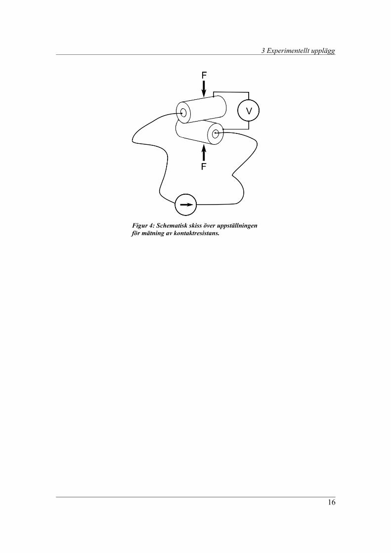
Kontaktresistansen bestämdes genom uppmätning av potentialfallet över en kontakt varigenom
en konstant ström drevs. En skiss över experimentuppställningen presenteras i figur 4.
Kontakten bestod av två korslagda cylindrar. Den ena cylindern, referenscylindern, var belagd
med ett tjockt silverskikt och den andra var belagd med filmen som skulle undersökas ovanpå
ett spärrlager av nickel. Kontaktresistansen bestämdes för tre olika sammanpressande krafter;
40, 100 och 300 N. Vid varje kraft mättes potentialfallet för sex olika strömmar; ±1 ,±3 och ±5
A.
15
3 Experimentellt upplägg
Figur 4: Schematisk skiss över uppställningen för mätning av kontaktresistans.
16
4 Resultat och diskussion
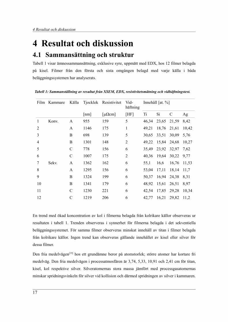
4 Resultat och diskussion4.1 Sammansättning och strukturTabell 1 visar ämnessammansättning, exklusive syre, uppmätt med EDX, hos 12 filmer belagda
på kisel. Filmer från den första och sista omgången belagd med varje källa i båda
beläggningssystemen har analyserats.
Tabell 1: Sammanställning av resultat från XSEM, EDX, resistivitetsmätning och vidhäftningstest.
Film Kammare Källa Tjocklek Resistivitet Vid-häftning
Innehåll [at. %]
[nm] [µΩcm] [HF] Ti Si C Ag
1 Konv. A 955 159 5 46,34 23,65 21,59 8,42
2 A 1146 175 1 49,21 18,76 21,61 10,42
3 B 698 139 5 30,65 33,51 30,09 5,76
4 B 1301 148 2 49,22 15,84 24,68 10,27
5 C 778 156 6 35,49 23,92 32,97 7,62
6 C 1007 175 2 40,36 19,64 30,22 9,77
7 Sekv. A 1362 162 6 55,1 16,6 16,76 11,53
8 A 1295 156 6 53,04 17,11 18,14 11,7
9 B 1324 199 6 50,37 16,94 24,38 8,31
10 B 1341 179 6 48,92 15,61 26,51 8,97
11 C 1230 221 6 42,54 17,85 29,28 10,34
12 C 1219 206 6 42,77 16,21 29,82 11,2
En trend med ökad koncentration av kol i filmerna belagda från kolrikare källor observeras ur
resultaten i tabell 1. Trenden observeras i synnerhet för filmerna belagda i det sekventiella
beläggningssystemet. För samma filmer observeras minskat innehåll av titan i filmer belagda
från kolrikare källor. Ingen trend kan observeras gällande innehållet av kisel eller silver för
dessa filmer.
Den fria medelvägen[19] hos ett grundämne beror på atomstorlek; större atomer har kortare fri
medelväg. Den fria medelvägen i processatmosfären är 3,74, 5,33, 10,91 och 2,41 cm för titan,
kisel, kol respektive silver. Silveratomernas stora massa jämfört med processgasatomernas
minskar spridningsvinkeln för silver vid kollision och därmed spridningen av silver i kammaren.
17
4 Resultat och diskussion
Då avståndet mellan substrat och sputterkälla i den sekventiella kammaren var 5 cm i denna
studie försummas spridningarna av samtliga ämnen och direkt överföring av material från
sputterkällan antas.
Sammansättningarna i filmerna belagda i den sekventiella kammaren förväntas enligt
föregående resonemang vara ungefär samma som i respektive källa. Filmerna belagda i den
konventionella kammaren där avståndet var 8 cm förväntas ha en något högre koncentration av
kol då de övriga ämnena spridits mer under beläggning. En sänkning av processtrycket i den
konventionella kammaren hade motverkat detta fenomen.
Den generella diskrepansen mellan uppmätta ämnessammansättningar och respektive
specificerade källinnehåll antas främst bero på tillkortakommanden hos analystekniken vilka
diskuterades i kapitel 3.4.
Variationen i uppmätt ämnessammansättning mellan filmena belagda i det konventionella
systemet härrör från från tjockleksskillnaderna hos filmerna i kombination med tidigare nämnda
begränsningar hos analysmetoden.
Figur 5 visar en serie av röntgendiffraktogram. Filmer från den sista omgången belagd med
varje källa från båda beläggningssystemen presenteras. Röntgendiffraktionsanalysen visar
reflexer från titankarbid och silver. Topparna är breda och av låg intensitet vilket antyder små
korn. Detta stöds även av XSEM. Svaga reflexer från titankarbid har observerats tidigare från
liknande filmer innehållande silver[12].
Inga toppar framträder ur diffraktogrammen för filmerna belagda från den minst kolhaltiga
källan. Detta antyder väldigt små korn eller helt amorf struktur. En jämförelse av
titankarbidreflexernas jämbördes intensiteter hos filmerna belagda med de kolrikare källorna
visar att intensiteten hos topparna TiC (111) och TiC (220) ökar jämfört med toppen TiC (200)
då kolhalten i sputterkällan ökar. Denna förändring i textur har observerats vid tidigare
forskning[7, 8, 10 & 20]. Förändringen har i dessa fall skett vid ett kolinnehåll i intervallet 50-70 at. %
i förhållande till totalt kol-titan innehåll. Detta styrker resonemanget om att kolinnehållet i
filmerna i detta arbete är likt det i respektive källa.
Ingen distinkt skillnad kan observeras mellan titankarbidtopparnas bredd från filmerna belagda
med de olika källorna. En kvalitativ bedömning gällande beroendet av källans kolhalt för
titankarbidkornens storlek är därmed inte möjlig att göra.
Reflexer från silver framträder endast ur diffraktogrammet för film 4 vilket indikerar att silver
inte agglomereras i filmerna. Detta överensstämmer med tidigare forskning[12] som säger att
18

4 Resultat och diskussion
agglomeration av silver först sker vid en silverhalt närmare 15 at. % och där över.
Figur 5: Resultat från XRD-analys. Filmerna 2 – 6 är belagda i det konventionella beläggningssystemet. Filmerna 8 – 12 är belagda i det sekventiella beläggningssystemet. Notera den logaritmiska intensitetsskalan.
Filmtjocklekarna, uppmätta med XSEM, som presenteras i tabell 1 är generellt en µm. En
jämförelse mellan tjocklekarna hos filmerna belagda med de olika sputterkällorna visar att
källor med högre innehåll av kol ger lägre beläggningshastighet. Detta är väntat då kol har lägst
sputterutbyte av de inblandade ämnena. Tjocklekarna hos filmerna belagda i det konventionella
systemet varierar kraftigt. Filmerna från de första omgångarna belagda med varje sputterkälla är
19
θ

4 Resultat och diskussion
betydligt tunnare än filmerna från de sista omgångarna.
Tjockleksskillnaden beror antagligen på föroreningar i kammaren. Vid byte av källa är
kammaren öppen för atmosfär under en längre period varvid gas adsorberar på källan och
kammarväggar. Den första omgången belagd med varje källa är påverkad av detta. Byte av
substrat går relativt snabbt och sker då kammaren är varm vilket gör att klart mindre gas
adsorberar än under källbyte. Tjockleken påverkas av detta enligt resonemanget i sektion 3.1.
Figur 6: SEM-bilder (XSEM) på filmerna 1 t.o.m. 6 belagda i det konventionella beläggningssystemet..
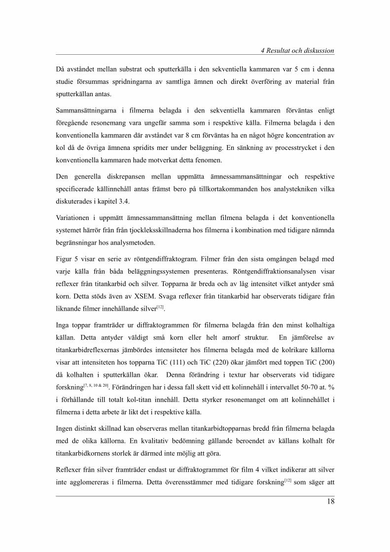
Figurerna 6 och 7 visar XSEM-bilder på filmer belagda under första och sista omgången med
varje källa i båda beläggningssystemen. Inga titankarbidkorn framträder ur bilderna och
filmerna ser kompakta ut. Filmerna 4 och 10 utmärker sig då de visas ha kolumnära porer. Film
4 innehåller dessutom urskiljningar. Hög sekundärelektonintensitet antyder att urskiljningarna
utgörs av silver vilket även stöds av diffraktogtrammet i figur 5. Urskiljningen av silver i film 4
beror på silverhalten[12] och på att filmen är porös vilket tillåter migration och agglomerering av
silver. Jämförelsevis har film 2 har samma silverhalt, ingen porositet och heller ingen
urskiljning av silver.
20
43
5
21
6
4 Resultat och diskussion
Figur 7: SEM-bilder (XSEM) på filmerna 7 t.o.m. 12 belagda i det sekventiella beläggningssystemet. De svarta ränderna är SiO2 från substraten.
4.2 Elektriska och mekaniska egenskaperTabell 1 visar uppmätt resistivitet för varje film. Överlag har filmerna en resistivitet på 140 -220
µΩcm. En jämförelse mellan resistiviteten hos filmer belagda med olika källor visar att en högre
kolhalt i källan ger högre resistivitet hos filmen. Detta stämmer med tidigare forskning[7 & 9] och
förklaras dels med att mer kol ger storleksmässigt mindre titankarbidkorn som sprider
elektronerna mer och dels med ökad förekomst av att amorft kol mellan kornen som fungerar
som isolator. I detta arbete finns inga tecken på mindre titankarbidkorn vilket antyder en ökad
förekomst av kol i den amorfa fasen.
Vidare har filmerna belagda i det sekventiella systemet högre resistivitet än filmerna belagda i
det konventionella. Sämre värmning i det sekventiella systemet skulle kunna vara en förklaring
då detta ger storleksmässigt mindre korn[16]. Avsaknaden av värmare är den främsta orsaken till
sämre värmning i det sekventiella systemet men även lägre etsfrekvens påverkar negativt.
Resultaten från Rockwellindentation presenteras i tabell 1. Ingen trend gällande vidhäftning går
att urskilja efter en jämförelse av resultat från källor.
21
109
87
11 12

4 Resultat och diskussion
Filmerna belagda i det konventionella beläggningssystemet har bättre vidhäftning än filmerna
belagda i det sekventiella. Detta beror sannolikt på lägre ets-frekvens i det sekventiella systemet
vilket leder till att ett tunt lager av orenheter som förhindrar kemisk bindning mellan film och
substrat samt en mindre ruggad yta som leder till sämre mekanisk bindning.
En jämförelse av vidhäftningen för filmer belagda i den första omgången för varje källa i det
konventionella systemet med filmer belagda i den sista omgången visar att vidhäftningen har
förbättras avsevärt efter fem omgångar. Samma jämförelse för filmer belagda i det sekventiella
systemet visar inget sådant fenomen. Den förbättrade vidhäftningen för filmer belagda i det
konventionella systemet kan förklaras med sänkt bastryck vilket har lett till mindre adsorberad
gas på substraten och bättre kemisk bindning mellan substrat och film. Att vidhäftningen inte
ändras för filmer belagda i det sekventiella systemet beror på att etsprocessen varit undermålig,
bakgrundstryck har inte förändrats märkbart.
Kontaktresistansen för filmerna belagda i den konventionella kammaren presenteras i tabell 2.
Filmerna belagda från den kolrikaste källan har lägre kontaktresistans än filmer belagda med de
övriga källorna. Tidigare undersökningar[7] har visat att en högre kolhalt bidrar till ökad
duktilitet vilket bör ge större kontaktpunkter och lägre kontaktresistans. En ökad andel kol i den
amorfa fasen ligger troligen bakom detta fenomen.
Vidare är kontaktresistansen för filmerna belagda i den sista omgången för respektive källa
lägre än för filmerna belagda i den första. Detta står troligen i samband med vidhäftningen
eftersom dålig vidhäftning i detta fall är kopplat till förekomsten av ett isolerande skikt mellan
film och substrat.
Tabell 2: Uppmätt kontaktresistans mot en silveryta.
Film Kontaktresistans [mΩ]
40 N 100 N 300 N 1 26,5 10,3 1,91
2 2,07 1,42 0,633
3 5,45 4,30 2,40
4 2,77 1,32 0,467
5 0,820 0,312 0,112
6 5,41 0,408 0,0928
22

5 Slutsatser
5 SlutsatserFrån resultaten i detta arbete kan konstateras att en ökning av kol i sammansatta sputterkällor av
Ti-Si-C-Ag ger kolrikare filmer. Tillväxten av titankarbid ökar och företrädd tillväxtriktning
ändras från 200 till 111. Agglomerationen av silver tilltar inte med ökad kolhalt. Mängden kol i
den amorfa fasen mellan kornen tycks tillta vilket leder till högre resistivitet för filmen men
även ökad duktilitet vilket sänker kontaktresistansen.
Kolets låga sputterutbyte leder till att beläggningstakten minskar med ökat innehåll av kol i
källan.
6 RekommendationerAnalysen av filmernas sammansättning och struktur har i detta arbete varit begränsad till XRD,
SEM och EDX. I synnerhet har EDX i detta sammanhang varit en olämplig teknik för
sammansättningsanalys. Fortsatt arbete skulle med fördel kunna använda ERDA (Elastic Recoil
Detection Analysis) med guldjoner för sammansättningsanalys. ERDA är särskilt lämplig då alla
inblandade ämnen går att kvantifiera. Dessutom med avseende på djup.
Utökad information om kornstorlek och den amorfa matrisen fås med hjälp av TEM
(Transmission Electron Microscopy). En sådan analys kan svara på hur kornstorleken beror på
ökat innehåll av kol samt om den amorfa fasen förändras.
XPS (X-ray Photoelectron Spectroscopy) kan ge information om bindningsenergier och därmed
hur mycket av kolet som binds till titan i titankarbid och hur mycket som binds till sig själv
alternativt till kisel i den amorfa fasen.
Kontaktresistans vid lägre sammanpressande kraft är av intresse att studera då många kontakter
för konsumentelektronik används vid låga sammanpressande krafter. Även förändring av
kontaktresistans efter nötning är av stort intresse att studera eftersom guldets dåliga prestanda
vid sådan behandling är en anledning till att byta till nanokomposit Ti-Si-C-Ag som
kontaktmaterial.
23

7 Tack
7 TackJag vill utfärda ett tack till följande personer som har varit till hjälp under arbetets gång:
Lars Hultman, min examinator och personen som presenterade Impact för mig.
Hans Högberg, min handledare som rätat ut ett och annat krokigt resonemang.
Erik Nelsson min opponent som har stått ut med en ständigt uppskjuten deadline.
Henrik Ljungcrantz VD på Impact Coatings.
Jonas Lauridsen som tagit sig tid att göra ytresistansmätningen åt mig och även boka
röntgendiffraktometern i tid och otid.
Fredrik Eriksson och Thomas Lingefelt som slipat mina färdigheter kring XRD och Svepet.
Erik O som lärt mig allt som går att veta om Tintin.
Axel, Torbjörn, Roger, Matsa och Simon Å på Impact som har utgjort bollplank för stort och
smått kring tunnfilmsfysik och sputtring.
Jessica som för ljus och glädje och mina föräldrar som varje gång jag ringer frågar ”du tänker
väl bli klar?”
24
8 Referenser
8 Referenser
[1] Vepřek, S; Reiprich, S, Thin Solid Films 268 64-71 (1995)
[2] Vepřek, S; Haussmann, M; Reiprich, S, Journal of Vacuum and Science Technology A 14 46-51 (1996)
[3] Voevodin, A, A; Capano, M, A; Laube, S, J, P; Donley, M, S; Zabinski, J, S, Thin Solid Films 298 107-115 (1996)
[4] Voevodin, A, A; Prasad, S, V; Zabinski, J, S, Journal of Applied Physics 82 855-858 (1997)
[5] Voevodin, A, A; Zabinski, J, S, Journal of materials Science 33 319-327 (1998)
[6] Stüber, M; Leiste, H; Ulrich, S; Hollck, H; Schild, D, Surface and Coatings Technology 150 218-226 (2001)
[7] Gulbiński, W; Mathur, S; Shen, H; Suszko, T, Gilewicz, A; Warcholiński, B, Applied Surface Science 239 302-310 (2004)
[8] Zehnder, T; Patscheider, J, Surface and Coating Technology 133-134 138-144 (2000)
[9] Lewin, E; Wilhelmsson, O; Jansson, U, Journal of Applied Physics 100 054303 (2006)
[10] Zehnder, T; Matthey, J; Schwaller, P; Klein, A; Steinmann, P-A; Patscheider, J, Surface and Coatings Technology 163-164 238-244 (2003)
[11] Eklund, P; Emmerlich, J; Högberg, H; Wilhelmsson, O; Isberg, P; Birch, J; Persson, P, O, Å; Jansson, U; Hultman, L, Journal of Vacuum Science and Technology B 23 2486-2493 (2005)
[12] Eklund, P; Joelsson, T; Ljungcrantz, H; Wilhelmsson, O; Czigány, Zs; Högberg, H; Hultman, L, Surface & Coatings Technology 201 6465-6469 (2007)
[13] Endrino, J, L; Naninaparampil,J,J; Krzanowski, J, E, Surface and Coatings Technology 157 95-101 (2002)
[14] Yao, S, H; Su, Y, L; Kao, W, H; Cheng, K, W, Surface and Coatings Technology 201 2520-2526 (2006)
[15] Holm, Ragnar, Electric Contacts 4th ed., Springer-Verlag, Berlin, Heidelberg & New York, (1967)
[16] Ohring, Milton, Materials science of thin films 2nd ed., Academic press, San Diego & London, (2002)
[17] Nordling, Carl; Österman, Jonny, Physics Handbook for Science and Engineering 7th ed., Studentlitteratur, Lund, (2004)
[18] VDI Guideline 3198, VDI-Handbuch für Betriebstechnikm, Teil 3 , VereinDeutscher Ingenieure, Düsseldorf, (1992)
[19] Roth, A, Vacuum Technology , Elsevier, Amsterdam, (1990)
[20] Voevodin, A, A; Capano, M, A; Laube, S, J, P; Donley, M, S; Zabinski, J, S, Thin Solid Films 298 107-115 (1997)
25

Abstract
AbstractToday gold is used as contact material on electric contacts for low current applications. Gold,
however, has low wear resistance, is expensive and environmentally stressful to produce. An
alternative contact material to gold is nano composite Ti-Si-C-Ag deposited with DC-magnetron
sputtering. Nano composite Ti-Si-C-Ag has so far been deposited by a compound Ti-Si-C
sputter target with a separate Ag target.
In this work films have been deposited by three different compound Ti-Si-C-Ag targets with
three different carbon contents. The films have been deposited in two separate PVD systems:
One conventional batch loaded and one sequential with a load-lock.
The phase- and elemental composition of the films has been studied with XRD and EDX
respectively. Thickness and microstructure have been analysed with SEM. Adhesion and
resistivity have been analysed with Rockwell indentation and surface resistivity measurement
with four point probe. Contact resistance has also been studied to a limited extent.
The work shows that the increment of carbon content in the target yields more carbon rich films
with larger titanium carbide crystallites. The resistivity is increasing due to an increased
amorphous phase between the crystallites but the contact resistance is decreasing due to a more
ductile film.
27

Abbreviations
AbbreviationsBelow follows a list of abbreviations used in the thesis and their respective meaning. Elements
and simple compounds of such are in the thesis denoted according to convention and is thus not
occurring in the list below. The same applies for physical entities.
EDX Energy Dispersive X-ray Analysis
ERDA Elastic Recoil Detection Analysis
PVD Physical Vapor Deposition
SEM Scanning Electron Microscope(-y)
TEM Transmission Electron Microscope(-y)
XRD X-ray diffraction
XSEM Cross sectional SEM
28

Table of contents
Table of contents Abstract.....................................................................................................................................27
Abbreviations............................................................................................................................28
Table of contents........................................................................................................................29
1 Introduction.............................................................................................................................301.1 Multifunctional coatings of nanocomposite.....................................................................301.2 Aim..................................................................................................................................311.3 Constrictions....................................................................................................................31
2 Theory.....................................................................................................................................322.1 Electrical contacts............................................................................................................322.2 Solid state........................................................................................................................322.3 DC-magnetron sputtering................................................................................................332.4 Scanning electron microscopy.........................................................................................342.5 Energy dispersive x-ray analysis.....................................................................................352.6 X-ray diffraction..............................................................................................................36
3 Experimental details................................................................................................................383.1 Depositing systems..........................................................................................................383.2 Deposition process..........................................................................................................403.3 Substrates........................................................................................................................403.4 Characterization of structure and composition................................................................403.5 Characterization of mechanical and electrical properties.................................................41
4 Results and discussion.............................................................................................................424.1 Composition and structure...............................................................................................424.2 Electrical and mechanical properties...............................................................................47
5 Conclusions.............................................................................................................................49
6 Recommendations...................................................................................................................49
7 Acknowledgments...................................................................................................................50
8 References...............................................................................................................................51
29
1 Introduction
1 IntroductionToday the most common design of an electrical contact for low current applications is a layered
structure composed of a structural material on the bottom and two overlying functional
materials. The structural material is the load bearing structure and hence decides the geometrical
form of the contact. Copper alloys are the most common materials for this purpose since they're
relatively inexpensive as well as easy to process. The two functional layers are usually
constituted of gold and nickel. Gold is used as contact material due to its low resistivity, high
ductility and chemical inertness. These properties results in large electrically conducting contact
spots and thus a low contact resistance. Copper easily migrates in gold whence a barrier layer is
needed. Nickel is often used as a diffusion barrier since nickel also has decent conductivity
combined with hardness, which gives the contact material improved wear resistance.
Gold, however, has limitations as the metal is expensive and environmentally stressful to
extract. The metal also has poor wear resistance which leads to a contact with hight ware rate.
These shortcomings implies that gold should be replaced by some other material that is less
expensive, more environmentally friendly and has a longer lifetime.
Maxphase™ by the company Impact Coatings AB, Linköping, Sweden, is an alternative to gold.
Maxphase™ is a multifunctional coating consisting of nano crystallites of titanium carbide and
silver in a matrix of amorphous silicon carbide (nc-TiC/Ag/a-SiC). Maxphase™ is a hard
coating with good wear resistance. In addition the material system also has high electric
conductivity.
1.1 Multifunctional coatings of nanocompositeIt's known since early 1990's that films of nanocrystallites in an amorphous matrix can show
extreme hardness[1 & 2]. For example films of nc-TiC/a-C, deposited by either reactive PVD from
a single Ti-source or conventionally by separate Ti- and C-sources, have proven to be very hard
as well as ductile[3, 4, 5, 6, 7 & 8]. Studies have shown that these films conduct electric current and are
functional as contact material on electric contacts[9].
In the regime above 50 at. % of carbon content an increased amount of carbon decreases the
size of the titanium carbide crystallites. The films become more ductile and show lower
coefficient of friction but also poorer electric conductivity. If silicon is introduced as a ternary
element in the film, by sputtering from a separate Si-source, films of nc-TiC/a-SiC are
obtained[10]. These films exhibit larger crystallites of titanium carbide along with increased
30

1 Introduction
conductivity which supports the previous line of argument.
Variation in chemical composition of the films previously presented is mainly achieved by
regulating the power over the individual sputter sources along with regulating the flux of the
possible reactive gas. This is an experimental setup fitting deposition in a laboratory whereas
industrial applications requires a minimum of sputter sources. Hence, the industry is in need of
compound sources. Regulation of composition in films deposited from compound sources can
be achieved partly by altering the composition in the source material and partly by varying the
process pressure in the chamber,
Eklund et. al. have investigated the possibility to sputter films of nc-TiC/a-SiC from a
compound source with the composition 3Ti-1Si-2C[11] . The resulting films proved to be
proficient as contact material on electrical contacts. Eklund et. al. have also studied the effect of
the amount of silver in films deposited from a compound 3Ti-1Si-2C source and a separate
silver source[12]. The resistivity of the films decreased with increased contents of silver and other
research[13 & 14] has also shown that elements of silver have positive tribological effects on films
of carbides and nitrides.
1.2 AimPrevious research shows that variation of the amount of carbon in films of nc-TiC/a-C and nc-
TiC/a-SiC clearly affects the resistivity, hardness and surface morphology of the coatings.
Research of the corresponding causality for films with content of silver hasn't been done.
Sputtering from compound sources with contents of silver is also an unexplored area.
This thesis presents the results from investigations of elemental composition, phase composition
and resistivity of films deposited by DC-magnetron sputtering from three sources of Ti-Si-C-Ag
with varied composition.
The work has been carried out at the company Impact Coatings AB, Linköping, and is a part of
the company's research and development. The work has been conducted with focus on high film
growth rate under production like conditions.
1.3 ConstrictionsMy purpose is for the main part of the theses to be concise for the expert, but that the in thin
film physics uninitiated engineer shall be able to obtain a basic understanding of the content
through the theory presented i section 2
31

2 Theory
2 TheoryThis section contains a brief description of the terms and techniques mentioned in the thesis.
The accuracy of the text is the responsibility of the author.
2.1 Electrical contactsThe term electric contact concerns a releasable junction between two conductors apt to carry electric current[15] - Ragnar Holm
The interface between the two conductors constituting an electrical contact is consisting of
small discreet areas where the electrically conducting materials have physical contact. The
individual size and the number of these areas are dependent on the amount of gas adsorbed on
the conductors surfaces, the amount of this adsorbed gas that has reacted chemically and bound
to the surface in forms of sulfides or oxides, how uneven the most uneven contact surface is,
how ductile the most ductile surface is and by the applied force on surfaces in contact. The
compressing force makes the asperities penetrate possible sulfides and oxides as well as
deforming the asperities elastically and plastically. This increases the number of contact spots
and makes them larger.
The contact resistance (or constriction resistance), Rc, is the potential drop over the junction
divided by the current driven through it. As the term constriction resistance implies it's the
limited cross section area of the conductor that constitutes most of the contact resistance. The
accumulated area of all the contact spots is usually 1 % of the macroscopic area of the contact
thus being a considerable constriction of the conductance that is directly proportional to the
cross section of the conductor. The contact resistance is further dependent on the compressing
force and not the pressure which might be apparent. That is a consequence of the area of the
individual contact spots being linearly dependent on the compressing force.
Since the contact surfaces deform plastically the contact resistance with respect to the
compressing force is a hysteresis where the contact resistance for a releasable force is lower
than for the same compressing force.
2.2 Solid stateSimply viewed the atoms in a solid matter can be either arranged or not arranged. Are they not
arranged in a pattern the matter is said to be amorphous (Greek shapeless). If the atoms are
arranged in a pattern the space in which the pattern exist is called a crystal. If the extension of
the crystal is the same as that of a sample the sample is said to be monocrystalline. If the sample
32
2 Theory
is consistent of many small crystals the sample is said to be polycrystalline. The small crystals
are in this case called crystallites.
Figure 1: Sketches of different crystal structures. a) simple cubic, b) face centered cubic, c) body centered cubic och d) NaCl.
The type of structure the atoms in a crystal adopts depends on the type of binding interacting
between the atoms and at which temperature the crystal is formed. Common lattices are s.c.
(simple cubic), f.c.c. (face centered cubic) and b.c.c (body centered cubic) shown in figure 1. If
two elements are mixed other lattices can arise. An example of such is the NaCl-structure
named after the type of structure that forms when sodium and chloride atoms form a crystal. In
this case the Na- and Cl-atoms form an f.c.c. structure relative their own kind and the two
lattices are displaced half a volume diagonal from each other..
The side of the boxes in figure 1 is called the lattice parameter.
2.3 DC-magnetron sputteringDC-magnetron sputtering is a technique for depositing films on a bearing material (substrate).
The material being deposited on the substrate is evaporated in a controlled atmosphere of inert
noble gas and / or reactive gases. The expanding vapor eventually condensates on the substrate.
The evaporation occurs when the positive gas ions accelerate towards the negatively biased
sputter source. Upon the impact of the gas ions on the source a series of linear collisions in the
surface region of the source may cause emission of one or a few surface bound atoms.
33
a b
c d

2 Theory
Different elements sputter at different rates. The sputter yield is a measure of how liable an
element is to sputter and is defined as the average number of atoms emitted from a source per
inbound ion. The sputter yield varies with the mass of the incoming ion and its kinetic energy.
E.g. an Ar+ ion with 500eV kinetic energy sputters in average 3.2 Ag-atoms, 0.5 Si-atoms, 0.51
Ti-atoms or 0.12 C-atoms[16].
Sputtering from a compound sputter source with different elements the flux from the source will
have the same composition as the source in whole, ergo not effected by the the individual
sputter yields of the different elements. This is a consequence of the sputter process being
surface bound making the fast sputtered elements relatively depleted after which an equilibrium
is established.
Collisions occur between the expanding vapor and the surrounding atmosphere in between the
the sputter source and the substrate. The mean free path of an atom, i.e. the average distance
traveled by a molecule between collisions, is, in the context, upper most dependent of the size
and occurrence (pressure) of the concerned molecules. Classical mechanics yields that lighter
elements scatter more. This implies that such elements spread out more than heavier in the
deposition chamber, even though the frequency of collision is the reciprocal, and that their
concentration in the film hence is shifted down relative the heavier elements (given that the
substrate is placed right in front of the sputter source).
When an atom condenses on the substrate, before being bound to a position, it migrates across
the substrates surface. The higher the energy of the atom the lighter its mobility and hence the
higher its probability of sticking to a position resulting in a minimum potential energy. Since a
crystalline structure often results in the lowest potential energy an increased substrate
temperature will increase the size if the crystallites in the film. By applying a negative bias on
the substrate positive gas ions will bombard the film surface as well. This bombardment scatters
crystallites and reduces the size of the crystallites in the film. A too large negative bias results in
the bombarding ions starting to sputter away the film.
In order to maintain the sputter process a magnetic field with a certain geometry is required in
the chamber. The magnetic field is generated by the magnetron on which the sputter source is
mounted.
2.4 Scanning electron microscopyScanning electron microscopy is a technique for analysing micro structure and in some
extension elemental composition. In scanning electron microscopy (SEM) a beam of high
34

2 Theory
energetic electron sweeps across the sample being analysed. The electrons are usually thermally
emitted and focused on the sample by electromagnetic lenses. The result from SEM is obtained
in the form of a micrograph which intuitively can be interpreted as a photographic picture of the
analysed sample.
The micrograph depicts the intensity of detected electrons by indicating high intensity with light
hue and low with dark.
The detected electrons are either secondary, low energetic, knocked out from the atoms in the
sample by the electron beam, or backscattered, high energetic. The backscattered are those
electrons of the beam that have scattered backwards when interacting with the sample.
The backscattered electrons originates from a depth up to approximately 1 µm while the
secondary originates from a depth of a few nm. The difference in depth is caused by the
difference in energy of the electrons; he low energetic electrons from the depth of the sample
don't reach the surface.
The intensity of detected electrons depends on the element numbers of the atoms interacting
with the beam. A higher element number generally yields higher intensity of both backscattered
and secondary electrons. The sample topography also matters as shadow effects occur.
Different detectors are used for detecting backscattered and secondary electrons. Due to the low
energy of the secondary electrons they can be attracted by a positive bias. Hence a detector
reacting on these can be placed aside from the sample. There are however detectors mounted
right above the sample in the lens (InLens). InLens detectors are more suited for shorter
working distances than detectors placed aside from the sample as the electrons in the latter case
are obstructed by the lens.
2.5 Energy dispersive x-ray analysisEnergy dispersive x-ray analysis, or EDX, is a technique of analysis analysing the elemental
composition of a sample. This is performed by production of a spectrum over x-ray radiation
where the characteristic x-ray transitions of the elements appear as peaks. EDX hence requires
that the atoms in the sample are excited which usually is accomplished by the means of high
energetic electrons. For this reason EDX analysis is often conducted in connection to an SEM or
a TEM (transmission electron microscope). In an SEM with 20 keV electrons x-ray radiation is
detected from a depth of several µm and a cross section area above a µm for every spot the
electron beam hits. The technique has relatively low resolution in comparison with SEM
35
2 Theory
detecting secondary electrons.
Qualitative analysis is in principle simple to perform by EDX since it's only needed to identify
the characteristic x-ray transitions in the spectrum. Overlapping is, however, common and can
in practice make the qualitative analysis more complicated.
Quantitative analysis is all the harder to perform. Established algorithms exist for for this
purpose, such as the ZAF-method. Yet the quantitative analysis is often done by a computer
program. Prior to quantitative analysis the program should be calibrated against some known
substance. Quantitative analysis of light elements such as carbon and oxygen is so unreliable
that it in practice is meaningless.
2.6 X-ray diffractionX-ray diffraction or XRD measures distances between lattice-planes and presents the results in a
diffractogram. A lattice-plane is, in analogy with algebra, suspended by three atoms (not on a
line). In crystals where the order of the atoms is strict and periodic an abundance of equidistant
parallel planes exists, for every three atoms chosen. It's the distances between such neighboring
planes that are measured. The vast number of well defined equidistant planes in a crystal gives
rise to clear and sparse (with respect to the scattering angle) diffraction patterns when the lattice
is illuminated by photons with a wavelength in the same order of magnitude as the lattice
parameter. Usually Cu Kα x-rays of the wavelength ~1,54 Å are used. Positive interference is
manifested as reflexion peaks in the diffractogram.
The orientation of the planes relative to the atom base are indexed with three integers according
to the convention {hkl} and the distance between the planes in cubic structures is given by
equation 1 where a denotes the lattice parameter[17].
d hkl=a
h2k 2l 2 (1)
Depending on geometrical factors diffracion patterns don't appear from all planes. For f.c.c
structures diffraction only appears when h, k, and l all are either odd or even integers.
The distance between the lattice planes is measured with the angle 2θ, where θ, somewhat
simplified, corresponds to the angle of incidence of the x-rays from the tangent of the sample
surface and 2θ thus is the sum of the angle of incidence and the angle of reflection. Equation 2
where is the wavelength of the x-rays, n is an integer multiple (usually n=1) and λ θ = 2θ/2
holds[17].
36

2 Theory
d hkl=n 2sin (2)
If the sample being analysed is mono crystalline is has to be aligned with a lattice plane in order
for the angle of incidence of the x-rays to equal the angle of reflection relative to that lattice
plane. If the sample isn't aligned no interference will be detected. This does not apply to
polycrystalline samples since there, generally, always are aligned crystallites in the sample
given that the orientation of all the grains are random. Are the grains not randomly orientated
some reflection peaks may be missing in the diffractogram. The material is in this case said to
be textured.
37
3 Experimental details
3 Experimental detailsIn this work coatings have been grown from three sputter sources of Ti-Si-C-Ag with
compositions according to the appendix. The sources are denoted A, B and C. The source A has
the lowest content of carbon and the source C has the highest. The ratio of the quantity of
substance titanium:silicon are equal for all sources as well as the absolute quantity of substance
of silver.
In the work a total of 30 batches of substrates were deposited; ten with each source divided over
to depositing systems.
3.1 Depositing systemsFilms were grown in two different deposition systems: One conventional schematically depicted
in figure 2 and one sequential, of the type Inline Coater, depicted in figure 3.
The conventional deposition system consists of a single large chamber. The chamber is
equipped with a heater that heats the samples and partly desorbs gas from the chamber walls.
The entire conventional chamber is ventilated when coated samples are exchanged with
uncoated. At ventilation gas adsorbs on sources and chamber walls which along with a large
chamber volume makes it harder to reach low base pressure. Films deposited in high base
pressure are expected to be thinner since gas adsorbs on the source and lowers the sputter rate as
well as to contain more oxygen being bound in the film during growth.
38

3 Experimental details
Figure 2: Schematic drawing of the conventional depositing system. Loading is done by the bottom being opened. The sputter source is situated on the chamber wall.
The sequential deposition system is constituted by a load-lock and the deposition chambers.
Changing of the substrates is performed in the load lock and a revolver transports the substrates
between the evacuated load-lock and the deposition chambers. The depostition chambers are
constantly in vacuum which results in relatively little gas adsorbing on the sources and chamber
walls. Condensation heat from the sputter vapor and heat from etch are the only sources of heat
in the sequential system.
Figure 3: Schematic drawing of the Inline Coater. Batch loading is done in the load-lock (the proximate cell). After pump down of the load-lock the samples are rotated to the deposition chamber. The sputtersource is situated in the chamber ceiling.
39
Sputter source
Chamber bottom being opened and closed
Load lock Samples being rotated to next chamber
Sputter source

3 Experimental details
3.2 Deposition processThe deposition process with the whole set of parameters is presented in the appendix.
3.3 SubstratesIn the conventional chamber a Si-wafer (100) with an approximately 150 nm thick SiO2 layer, a
Si-wafer without SiO2 layer, a nickel plated copper cylinder and a piece of high speed steel were
coated. In the sequential chamber a Si-wafer (100) with an approximately 150 nm thick SiO2
layer and a piece of high speed steel were coated.
The piece of high speed steel was polished with grit 1200 paper prior to coating. There after the
high speed steel was washed together with the nickel plated copper cylinders in a washing
machine of the type Allka-Jet C BSRTU-M 1111 with a for the machine approved program.
Immediately after washing possibly remaining moist was blown away from the details with
clean compressed air. The high speed steel and the nickel plated details were stored in a drying
cupboard for up to two weeks prior to coating. The silicon details didn't undergo any treatment
before coating.
3.4 Characterization of structure and compositionThe phase composition of the films were studied with X-ray diffraction in a Philips MRD
diffractometer with Cu Kα radiation. The films were deposited on either Si (100) or SiO2/Si
(100) substrates. The X-ray tube was set on 40 kV and 40 mA. Parallel beam optics was used
and the beam was shielded with 2 x 2 mm slits. The 2θ interval was 20-80˚ with a step size of
0.03˚ and a dwell time of 5.25 s. An ω-2θ scan was performed over the the substrate Si (400)
peak in order to line up the sample thus maximizing the peak reflection intensity. The PCPDF
cards 32-1386 and 04-0783 were used as reference for TiC and Ag respectively. The samples
were mounted with double sided adhesive tape on a objective glass and were cleansed with
isopropanol prior to measuring.
The cross sections of the films were studied with a scanning electron microscope (XSEM) to
determine the film thicknesses and to examine the micro structure. The microscope was of the
brand SEM Leo 1550. The working distance of the the electron beam was set to 4 mm, the
electron energy to 4 keV and the secondary electrons were detected with an InLens detector.
The substrates were either Si (100) or SiO2/Si(100).
The compositions of the the films were studied using energy dispersive X-ray analysis (EDX) in
connection to the same microscope mentioned above with a detector from Oxford of model
40

3 Experimental details
6901 with an ATW2 window. The software INCA suit version 4.09 was used to interpret the
obtained spectra. The working distance of the microscope was set to 10 mm, the electron energy
to 20 keV and INCA was calibrated against cobalt in order to make quantitative analysis of the
composition possible. The sample time for the spectra was 180 s. The substrates were the same
as for XSEM. The samples were mounted such that their planar surface was analysed.
EDX is not a suitable technique to detect light elements such as carbon and oxygen given their
characteristic X-rays, which are low energetic and attenuated on their way to the detector. The
XRD depth of analysis may also exceed the film thickness, hence a signal from the substrate can
be expected.
3.5 Characterization of mechanical and electrical properties The adhesion of the films to the substrate were determined by Rockwell indentation. The
durometer used was equipped with a 120˚ diamond tip. The applied force was 140 kg. Rockwell
indentation is a qualitative method for grading the adhesion of hard coating to steel. The results
from testing are arranged in a scale from HF 1 to HF 6 for good and poor adhesion
respectively[18].
The surface resistance was determined from four point probe measurements, model 280C from
Four Dimensions, at room temperature. The resistivity was obtained when the surface resistance
was multiplied with the film thickness.
The contact resistance was determined by measurement of the potential drop over a contact
through which a constant current was driven. A sketch over the experimental setup is presented
in figure 4. The contact consisted of two crossed cylinders. One of the cylinders, the reference
cylinder, was coated with a thick layer of silver and the other one was coated with the film to be
analysed on top of a nickel diffusion barrier. The contact resistance was determined for three
different compressing forces; 40, 100 and 300 N. For each force the potential drop was
measured for six different currents; ±1 ,±3 and ±5 A.
41
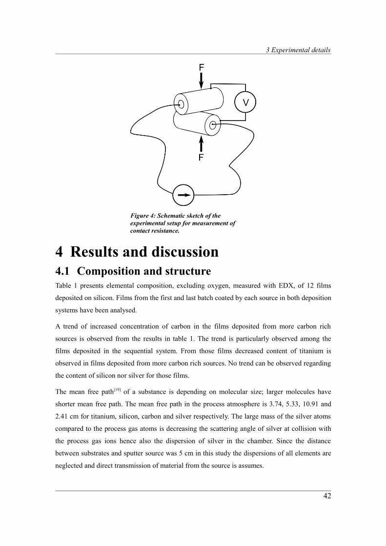
3 Experimental details
Figure 4: Schematic sketch of the experimental setup for measurement of contact resistance.
4 Results and discussion4.1 Composition and structureTable 1 presents elemental composition, excluding oxygen, measured with EDX, of 12 films
deposited on silicon. Films from the first and last batch coated by each source in both deposition
systems have been analysed.
A trend of increased concentration of carbon in the films deposited from more carbon rich
sources is observed from the results in table 1. The trend is particularly observed among the
films deposited in the sequential system. From those films decreased content of titanium is
observed in films deposited from more carbon rich sources. No trend can be observed regarding
the content of silicon nor silver for those films.
The mean free path[19] of a substance is depending on molecular size; larger molecules have
shorter mean free path. The mean free path in the process atmosphere is 3.74, 5.33, 10.91 and
2.41 cm for titanium, silicon, carbon and silver respectively. The large mass of the silver atoms
compared to the process gas atoms is decreasing the scattering angle of silver at collision with
the process gas ions hence also the dispersion of silver in the chamber. Since the distance
between substrates and sputter source was 5 cm in this study the dispersions of all elements are
neglected and direct transmission of material from the source is assumes.
42

4 Results and discussion
Table 1: Compilation of the results from XSEM, EDX, resistance measurements and adhesion tests.
Film Chamber Source Thick-ness
Resistivity Ad-hesion
Composition [at. %]
[nm] [µΩcm] [HF] Ti Si C Ag
1 Konv. A 955 159 5 46,34 23,65 21,59 8,42
2 A 1146 175 1 49,21 18,76 21,61 10,42
3 B 698 139 5 30,65 33,51 30,09 5,76
4 B 1301 148 2 49,22 15,84 24,68 10,27
5 C 778 156 6 35,49 23,92 32,97 7,62
6 C 1007 175 2 40,36 19,64 30,22 9,77
7 Sekv. A 1362 162 6 55,1 16,6 16,76 11,53
8 A 1295 156 6 53,04 17,11 18,14 11,7
9 B 1324 199 6 50,37 16,94 24,38 8,31
10 B 1341 179 6 48,92 15,61 26,51 8,97
11 C 1230 221 6 42,54 17,85 29,28 10,34
12 C 1219 206 6 42,77 16,21 29,82 11,2
The compositions in the films deposited in the sequential chamber are according to the previous
line of argument expected to be approximately the same as respective source. The films
deposited in the conventional chamber where the distance was 8 cm are expected to have a
slightly higher concentration of carbon since the other elements were more dispersed during
deposition. A reduction of the process pressure in the conventional chamber would have
counteracted this phenomenon.
The general discrepancy between measured elemental compositions and corresponding
specified source contents is assumed to foremost be due to the shortcomings of the method of
analysis discussed in chapter 3.4.
The variation in measured elemental composition among the films deposited in the conventional
chamber originates from the difference in thickness of the films combined with previously
mentioned limitations of the method of analysis.
Figure 5 presents a series of X-ray diffractograms. Films from the final batch deposited with
each source from both systems are presented. The X-ray diffraction analysis indicates
reflections from titanium carbide and silver. The peaks are wide and of low intensity implying
43
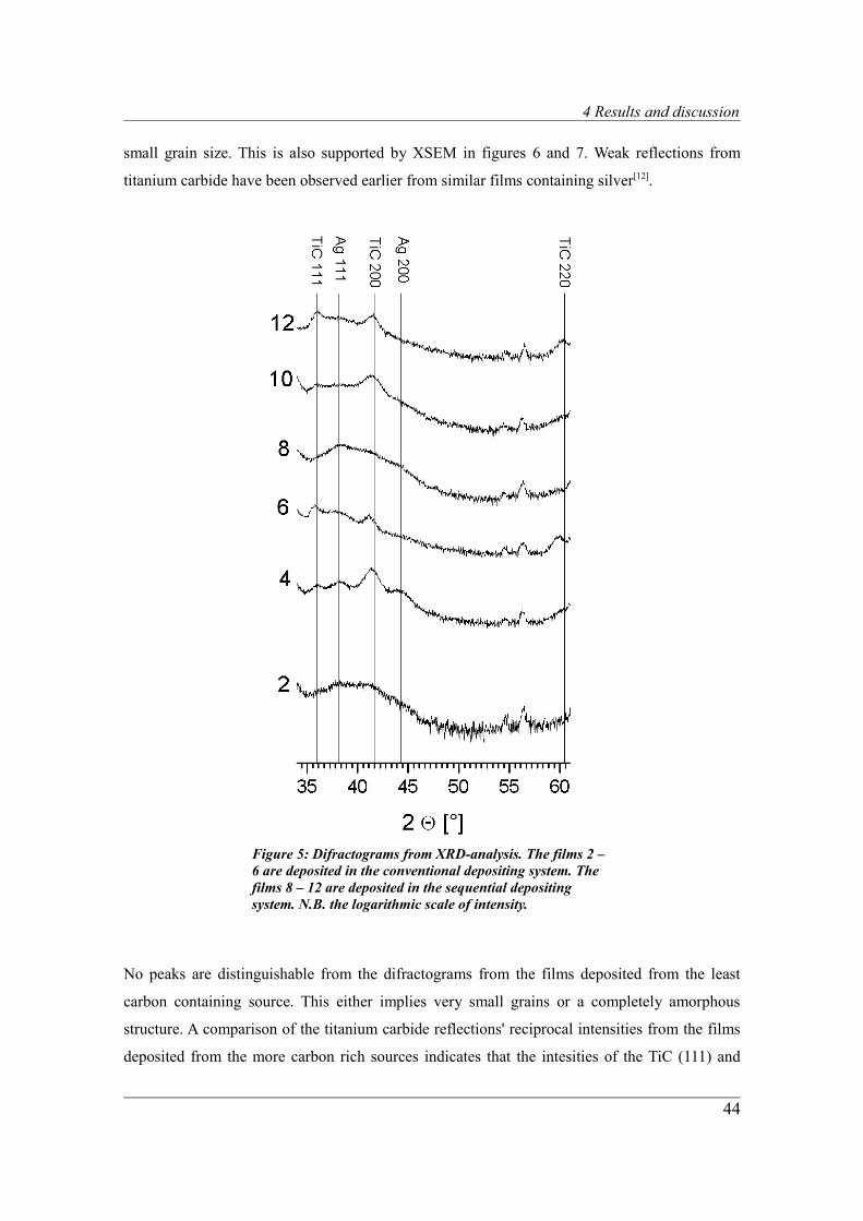
4 Results and discussion
small grain size. This is also supported by XSEM in figures 6 and 7. Weak reflections from
titanium carbide have been observed earlier from similar films containing silver[12].
Figure 5: Difractograms from XRD-analysis. The films 2 – 6 are deposited in the conventional depositing system. The films 8 – 12 are deposited in the sequential depositing system. N.B. the logarithmic scale of intensity.
No peaks are distinguishable from the difractograms from the films deposited from the least
carbon containing source. This either implies very small grains or a completely amorphous
structure. A comparison of the titanium carbide reflections' reciprocal intensities from the films
deposited from the more carbon rich sources indicates that the intesities of the TiC (111) and
44
θ
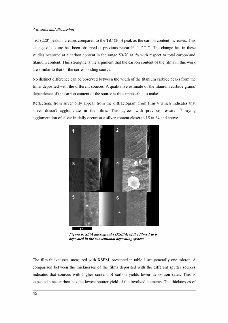
4 Results and discussion
TiC (220) peaks increases compared to the TiC (200) peak as the carbon content increases. This
change of texture has been observed at previous research[7, 8, 10 & 20]. The change has in these
studies occurred at a carbon content in the range 50-70 at. % with respect to total carbon and
titanium content. This strengthens the argument that the carbon content of the films in this work
are similar to that of the corresponding source.
No distinct difference can be observed between the width of the titanium carbide peaks from the
films deposited with the different sources. A qualitative estimate of the titanium carbide grains'
dependence of the carbon content of the source is thus impossible to make.
Reflections from silver only appear from the diffractogram from film 4 which indicates that
silver doesn't agglomerate in the films. This agrees with previous research[12] saying
agglomeration of silver initially occurs at a silver content closer to 15 at. % and above.
Figure 6: SEM micrographs (XSEM) of the films 1 to 6 deposited in the conventional depositing system..
The film thicknesses, measured with XSEM, presented in table 1 are generally one micron. A
comparison between the thicknesses of the films deposited with the different sputter sources
indicates that sources with higher content of carbon yields lower deposition rates. This is
expected since carbon has the lowest sputter yield of the involved elements. The thicknesses of
45
1
6
2
5
43
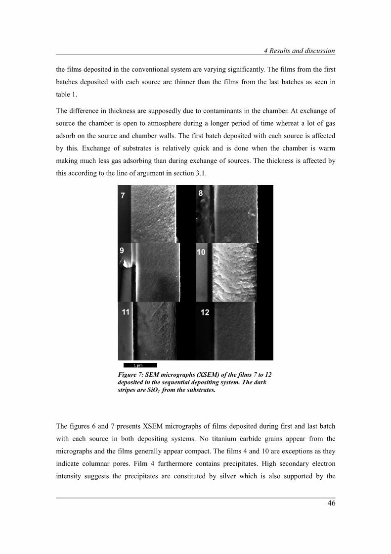
4 Results and discussion
the films deposited in the conventional system are varying significantly. The films from the first
batches deposited with each source are thinner than the films from the last batches as seen in
table 1.
The difference in thickness are supposedly due to contaminants in the chamber. At exchange of
source the chamber is open to atmosphere during a longer period of time whereat a lot of gas
adsorb on the source and chamber walls. The first batch deposited with each source is affected
by this. Exchange of substrates is relatively quick and is done when the chamber is warm
making much less gas adsorbing than during exchange of sources. The thickness is affected by
this according to the line of argument in section 3.1.
Figure 7: SEM micrographs (XSEM) of the films 7 to 12 deposited in the sequential depositing system. The dark stripes are SiO2 from the substrates.
The figures 6 and 7 presents XSEM micrographs of films deposited during first and last batch
with each source in both depositing systems. No titanium carbide grains appear from the
micrographs and the films generally appear compact. The films 4 and 10 are exceptions as they
indicate columnar pores. Film 4 furthermore contains precipitates. High secondary electron
intensity suggests the precipitates are constituted by silver which is also supported by the
46
9 10
87
11 12

4 Results and discussion
diffractogram in figure 5. The precipitation of silver in film 4 is due to the content of silver[12] in
combination with the film being porous which allows migration and agglomeration of silver.
For comparison film 2 has the same content of silver, no porosity nor silver precipitation.
4.2 Electrical and mechanical propertiesTable 1 present measured resistivity of each film. To summarize, the films have a resistivity of
140 – 220 µΩcm. A comparison between the resistivity of films deposited with different sources
indicate that a higher source carbon content yields a higher resistivity of the film. This concurs
with previous research[7 & 9] and is partly explained by more carbon giving smaller titanium
carbide grains scattering the electrons more and partly by an increased occurrence of amorphous
carbon in between the grains functioning as an insulator. In this work there are no indication of
smaller titanium carbide grains which implies an increased occurrence of carbon in the
amorphous phase.
Furthermore, the films deposited in the sequential system have higher resistivity than the films
deposited in the conventional. Less extensive heating in the sequential system may be an
explanation as it yields smaller grains[16]. The lack of a heater is the major cause to lower
heating in the sequential system but also lower etching frequency influences negatively.
The results from Rockwell indentation are presented in table 1. No trend regarding adhesion is
perceivable after a comparison of results from different sources.
The films deposited in the conventional system have better adhesion than the films deposited in
the sequential. This is probably due to lower etching frequency in the sequential system leading
to a thin layer of impurities inhibiting chemical bonding between film and substrate and also to
a less pronounced hill-locks surface leading to poorer mechanical binding.
A comparison of the adhesion of films deposited during the first batch for each source in the
sequential system with the adhesion of those deposited during the last batch shows that the
adhesion has improved remarkably after five batches. The same comparison between films
deposited in the sequential system shows no such phenomenon. The improved adhesion of the
films deposited in the conventional system can be explained by decreased base pressure which
has lead to less adsorbed gas on the substrates giving improved chemical bonding between
substrate and film. The adhesion not improving for films deposited in the sequential system is
due to an inferior etching process, the base pressure has not changed notably.
The contact resistances of the films deposited in the conventional system are presented in table
47
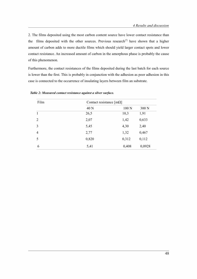
4 Results and discussion
2. The films deposited using the most carbon content source have lower contact resistance than
the films deposited with the other sources. Previous research[7] have shown that a higher
amount of carbon adds to more ductile films which should yield larger contact spots and lower
contact resistance. An increased amount of carbon in the amorphous phase is probably the cause
of this phenomenon.
Furthermore, the contact resistances of the films deposited during the last batch for each source
is lower than the first. This is probably in conjunction with the adhesion as poor adhesion in this
case is connected to the occurrence of insulating layers between film an substrate.
Table 2: Measured contact resistance against a silver surface.
Film Contact resistance [mΩ]
40 N 100 N 300 N 1 26,5 10,3 1,91
2 2,07 1,42 0,633
3 5,45 4,30 2,40
4 2,77 1,32 0,467
5 0,820 0,312 0,112
6 5,41 0,408 0,0928
48

5 Conclusions
5 ConclusionsFrom the results in this work it can be established that an increment of carbon in compound
sputter sources of Ti-Si-C-Ag yields more carbon content films. The growth of titanium carbide
grains increases and preferred orientation of growth is changed from 200 to 111. The
agglomeration of silver is not increasing with increased source carbon content. The amount of
carbon in the amorphous phase in between the grains seems to increase giving higher resistivity
but also more ductile films lowering the contact resistance.
The low sputter yield of carbon leads to the deposition rate decreasing with a higher source
carbon content.
6 RecommendationsThe analysis of the compositions and structures of the films have in this work been limited to
XRD, SEM and EDX. EDX in particular has in this context been an unsuitable technique for
composition analysis. Continued research might favorably use ERDA (Elastic Recoil Detection
Analysis) with gold ions for composition analysis. ERDA is particularly useful as all included
elements are possible to quantify. Furthermore with respect to depth.
Extended information of grain size and the amorphous matrix is obtained with the help of TEM
(Transmission Electron Microscopy). Such an analysis can tell how grain size depends on
increased content of carbon as well if the amorphous phase changes.
XPS (X-ray Photoelectron Spectroscopy) can give information of binding energies and thus how
much of the carbon is bound to titanium forming titanium carbide and how much is bound to
itself or silicon in the amorphous phase.
Contact resistance at lower compressing forces is of interest to study as many contacts for
consumer electronics are applied at low compressing forces. Also change of contact resistance
after wear is of great interest to study since the poor performance of gold at such treatment is a
reason for changing to nanocomposite Ti-Si-C-Ag as contact material.
49

7 Acknowledgments
7 AcknowledgmentsI would like to extend acknowledgments to the following persons that have been helpful during
the progress of this work:
Lars Hultman, my examiner and the person introducing Impact to me.
Hans Högberg, my supervisor who has straightened some twisted reasoning.
Erik Nelsson, my opponent who has endured a continuously postponed deadline.
Henrik Ljungcrantz, CEO of Impact Coatings.
Jonas Lauridsen who has taken time to measure the surface resistances and also booked the X-
ray diffractometer at all times.
Fredrik Eriksson and Thomas Lingefelt for teaching me the XRD and SEM.
Erik O for teaching me all that can possibly be known of Tintin.
Axel, Torbjörn, Roger, Matsa och Simon Å at Impact for bouncing ideas regarding large and
small of thin film physics and sputtering.
Jessica bringing light and joy and my parents, each time I call, asking “ you are going to finish,
right?”.
50

8 References
8 References[1] Vepřek, S; Reiprich, S, Thin Solid Films 268 64-71 (1995)
[2] Vepřek, S; Haussmann, M; Reiprich, S, Journal of Vacuum and Science Technology A 14 46-51 (1996)
[3] Voevodin, A, A; Capano, M, A; Laube, S, J, P; Donley, M, S; Zabinski, J, S, Thin Solid Films 298 107-115 (1996)
[4] Voevodin, A, A; Prasad, S, V; Zabinski, J, S, Journal of Applied Physics 82 855-858 (1997)
[5] Voevodin, A, A; Zabinski, J, S, Journal of materials Science 33 319-327 (1998)
[6] Stüber, M; Leiste, H; Ulrich, S; Hollck, H; Schild, D, Surface and Coatings Technology 150 218-226 (2001)
[7] Gulbiński, W; Mathur, S; Shen, H; Suszko, T, Gilewicz, A; Warcholiński, B, Applied Surface Science 239 302-310 (2004)
[8] Zehnder, T; Patscheider, J, Surface and Coating Technology 133-134 138-144 (2000)
[9] Lewin, E; Wilhelmsson, O; Jansson, U, Journal of Applied Physics 100 054303 (2006)
[10] Zehnder, T; Matthey, J; Schwaller, P; Klein, A; Steinmann, P-A; Patscheider, J, Surface and Coatings Technology 163-164 238-244 (2003)
[11] Eklund, P; Emmerlich, J; Högberg, H; Wilhelmsson, O; Isberg, P; Birch, J; Persson, P, O, Å; Jansson, U; Hultman, L, Journal of Vacuum Science and Technology B 23 2486-2493 (2005)
[12] Eklund, P; Joelsson, T; Ljungcrantz, H; Wilhelmsson, O; Czigány, Zs; Högberg, H; Hultman, L, Surface & Coatings Technology 201 6465-6469 (2007)
[13] Endrino, J, L; Naninaparampil,J,J; Krzanowski, J, E, Surface and Coatings Technology 157 95-101 (2002)
[14] Yao, S, H; Su, Y, L; Kao, W, H; Cheng, K, W, Surface and Coatings Technology 201 2520-2526 (2006)
[15] Holm, Ragnar, Electric Contacts 4th ed., Springer-Verlag, Berlin, Heidelberg & New York, (1967)
[16] Ohring, Milton, Materials science of thin films 2nd ed., Academic press, San Diego & London, (2002)
[17] Nordling, Carl; Österman, Jonny, Physics Handbook for Science and Engineering 7th ed., Studentlitteratur, Lund, (2004)
[18] VDI Guideline 3198, VDI-Handbuch für Betriebstechnikm, Teil 3 , VereinDeutscher Ingenieure, Düsseldorf, (1992)
[19] Roth, A, Vacuum Technology , Elsevier, Amsterdam, (1990)
[20] Voevodin, A, A; Capano, M, A; Laube, S, J, P; Donley, M, S; Zabinski, J, S, Thin Solid Films 298 107-115 (1997)
51