
Soiseek - 搜IC:全中文IC搜索引擎
123
搜IC:电子行业搜索门户 数据手册 行业新闻 技术文章 工程师博客 企业招聘 专业图书 技术问答 关注微博 联系我们
Transcript of Soiseek - 搜IC:全中文IC搜索引擎
July 2010 Doc ID 15962 Rev 5 1/122
1
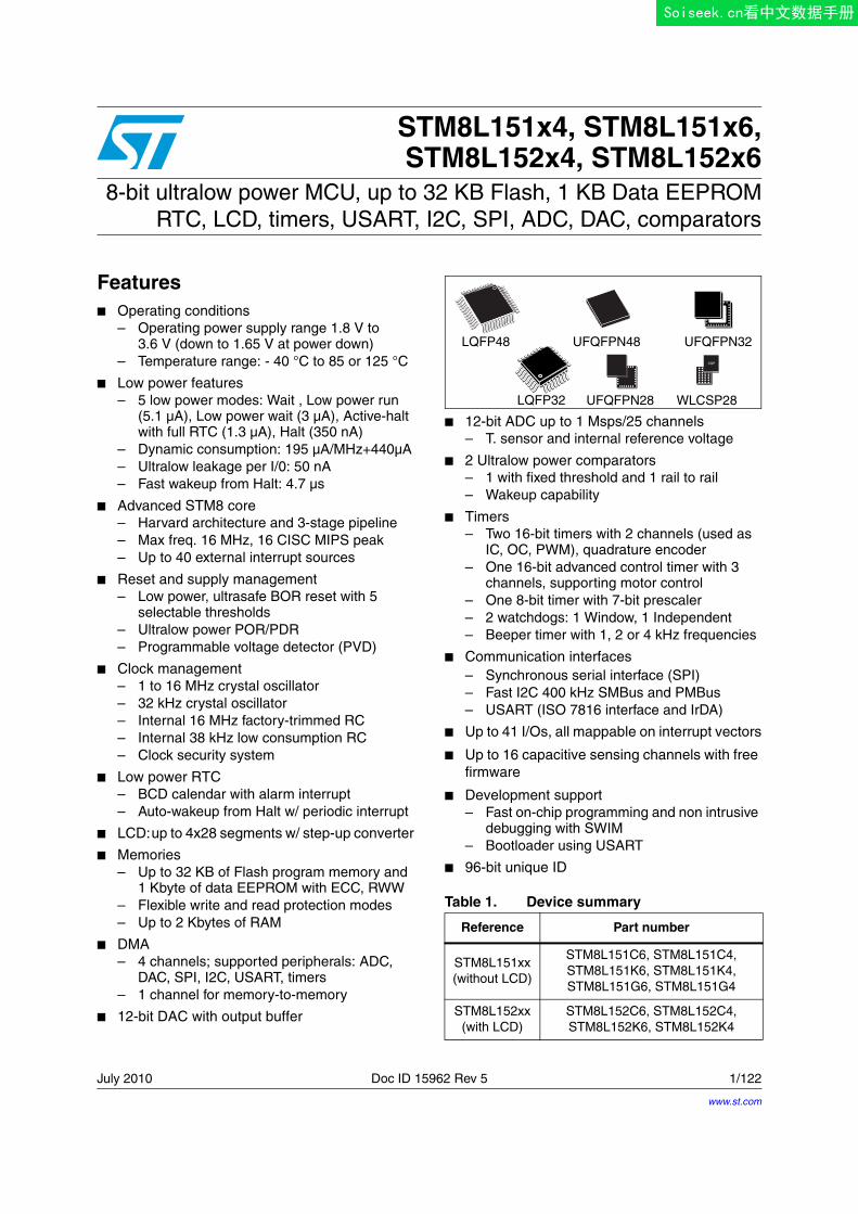
STM8L151x4, STM8L151x6,STM8L152x4, STM8L152x6
8-bit ultralow power MCU, up to 32 KB Flash, 1 KB Data EEPROMRTC, LCD, timers, USART, I2C, SPI, ADC, DAC, comparators
Features■ Operating conditions
– Operating power supply range 1.8 V to 3.6 V (down to 1.65 V at power down)
– Temperature range: - 40 °C to 85 or 125 °C
■ Low power features– 5 low power modes: Wait , Low power run
(5.1 µA), Low power wait (3 µA), Active-halt with full RTC (1.3 µA), Halt (350 nA)
– Dynamic consumption: 195 µA/MHz+440µA– Ultralow leakage per I/0: 50 nA– Fast wakeup from Halt: 4.7 µs
■ Advanced STM8 core– Harvard architecture and 3-stage pipeline– Max freq. 16 MHz, 16 CISC MIPS peak– Up to 40 external interrupt sources
■ Reset and supply management– Low power, ultrasafe BOR reset with 5
selectable thresholds– Ultralow power POR/PDR– Programmable voltage detector (PVD)
■ Clock management– 1 to 16 MHz crystal oscillator– 32 kHz crystal oscillator– Internal 16 MHz factory-trimmed RC – Internal 38 kHz low consumption RC – Clock security system
■ Low power RTC– BCD calendar with alarm interrupt– Auto-wakeup from Halt w/ periodic interrupt
■ LCD: up to 4x28 segments w/ step-up converter
■ Memories– Up to 32 KB of Flash program memory and
1 Kbyte of data EEPROM with ECC, RWW– Flexible write and read protection modes– Up to 2 Kbytes of RAM
■ DMA– 4 channels; supported peripherals: ADC,
DAC, SPI, I2C, USART, timers– 1 channel for memory-to-memory
■ 12-bit DAC with output buffer
■ 12-bit ADC up to 1 Msps/25 channels– T. sensor and internal reference voltage
■ 2 Ultralow power comparators– 1 with fixed threshold and 1 rail to rail – Wakeup capability
■ Timers– Two 16-bit timers with 2 channels (used as
IC, OC, PWM), quadrature encoder– One 16-bit advanced control timer with 3
channels, supporting motor control– One 8-bit timer with 7-bit prescaler– 2 watchdogs: 1 Window, 1 Independent – Beeper timer with 1, 2 or 4 kHz frequencies
■ Communication interfaces– Synchronous serial interface (SPI)– Fast I2C 400 kHz SMBus and PMBus– USART (ISO 7816 interface and IrDA)
■ Up to 41 I/Os, all mappable on interrupt vectors
■ Up to 16 capacitive sensing channels with free firmware
■ Development support– Fast on-chip programming and non intrusive
debugging with SWIM– Bootloader using USART
■ 96-bit unique ID
Table 1. Device summary
Reference Part number
STM8L151xx(without LCD)
STM8L151C6, STM8L151C4, STM8L151K6, STM8L151K4, STM8L151G6, STM8L151G4
STM8L152xx(with LCD)
STM8L152C6, STM8L152C4, STM8L152K6, STM8L152K4
UFQFPN48
LQFP32 UFQFPN28
UFQFPN32 LQFP48 CSP
WLCSP28
www.st.com
Soiseek.cn看中文数据手册
Contents STM8L151xx, STM8L152xx
2/122 Doc ID 15962 Rev 5
Contents
1 Introduction . . . . . . . . . . . . . . . . . . . . . . . . . . . . . . . . . . . . . . . . . . . . . . . . 9
2 Description . . . . . . . . . . . . . . . . . . . . . . . . . . . . . . . . . . . . . . . . . . . . . . . . 10
2.1 Device overview . . . . . . . . . . . . . . . . . . . . . . . . . . . . . . . . . . . . . . . . . . . . 11
2.2 Ultralow power continuum . . . . . . . . . . . . . . . . . . . . . . . . . . . . . . . . . . . . 12
3 Functional overview . . . . . . . . . . . . . . . . . . . . . . . . . . . . . . . . . . . . . . . . 13
3.1 Low power modes . . . . . . . . . . . . . . . . . . . . . . . . . . . . . . . . . . . . . . . . . . 14
3.2 Central processing unit STM8 . . . . . . . . . . . . . . . . . . . . . . . . . . . . . . . . . 14
3.2.1 Advanced STM8 Core . . . . . . . . . . . . . . . . . . . . . . . . . . . . . . . . . . . . . . 14
3.2.2 Interrupt controller . . . . . . . . . . . . . . . . . . . . . . . . . . . . . . . . . . . . . . . . . 15
3.3 Reset and supply management . . . . . . . . . . . . . . . . . . . . . . . . . . . . . . . . 16
3.3.1 Power supply scheme . . . . . . . . . . . . . . . . . . . . . . . . . . . . . . . . . . . . . . 16
3.3.2 Power supply supervisor . . . . . . . . . . . . . . . . . . . . . . . . . . . . . . . . . . . . 16
3.3.3 Voltage regulator . . . . . . . . . . . . . . . . . . . . . . . . . . . . . . . . . . . . . . . . . . 16
3.4 Clock management . . . . . . . . . . . . . . . . . . . . . . . . . . . . . . . . . . . . . . . . . 17
3.5 Low power real-time clock . . . . . . . . . . . . . . . . . . . . . . . . . . . . . . . . . . . . 18
3.6 LCD (Liquid crystal display) . . . . . . . . . . . . . . . . . . . . . . . . . . . . . . . . . . . 19
3.7 Memories . . . . . . . . . . . . . . . . . . . . . . . . . . . . . . . . . . . . . . . . . . . . . . . . . 19
3.8 DMA . . . . . . . . . . . . . . . . . . . . . . . . . . . . . . . . . . . . . . . . . . . . . . . . . . . . . 19
3.9 Analog-to-digital converter . . . . . . . . . . . . . . . . . . . . . . . . . . . . . . . . . . . . 19
3.10 Digital-to-analog converter (DAC) . . . . . . . . . . . . . . . . . . . . . . . . . . . . . . 20
3.11 Ultralow power comparators . . . . . . . . . . . . . . . . . . . . . . . . . . . . . . . . . . . 20
3.12 System configuration controller and routing interface . . . . . . . . . . . . . . . 20
3.13 Timers . . . . . . . . . . . . . . . . . . . . . . . . . . . . . . . . . . . . . . . . . . . . . . . . . . . 20
3.13.1 TIM1 - 16-bit advanced control timer . . . . . . . . . . . . . . . . . . . . . . . . . . . 21
3.13.2 16-bit general purpose timers . . . . . . . . . . . . . . . . . . . . . . . . . . . . . . . . 21
3.13.3 8-bit basic timer . . . . . . . . . . . . . . . . . . . . . . . . . . . . . . . . . . . . . . . . . . . 21
3.14 Watchdog timers . . . . . . . . . . . . . . . . . . . . . . . . . . . . . . . . . . . . . . . . . . . 22
3.14.1 Window watchdog timer . . . . . . . . . . . . . . . . . . . . . . . . . . . . . . . . . . . . . 22
3.14.2 Independent watchdog timer . . . . . . . . . . . . . . . . . . . . . . . . . . . . . . . . . 22
3.15 Beeper . . . . . . . . . . . . . . . . . . . . . . . . . . . . . . . . . . . . . . . . . . . . . . . . . . . 22
Soiseek.cn看中文数据手册
STM8L151xx, STM8L152xx Contents
Doc ID 15962 Rev 5 3/122
3.16 Communication interfaces . . . . . . . . . . . . . . . . . . . . . . . . . . . . . . . . . . . . 22
3.16.1 SPI . . . . . . . . . . . . . . . . . . . . . . . . . . . . . . . . . . . . . . . . . . . . . . . . . . . . . 22
3.16.2 I²C . . . . . . . . . . . . . . . . . . . . . . . . . . . . . . . . . . . . . . . . . . . . . . . . . . . . . 22
3.16.3 USART . . . . . . . . . . . . . . . . . . . . . . . . . . . . . . . . . . . . . . . . . . . . . . . . . . 23
3.17 Infrared (IR) interface . . . . . . . . . . . . . . . . . . . . . . . . . . . . . . . . . . . . . . . . 23
3.18 Development support . . . . . . . . . . . . . . . . . . . . . . . . . . . . . . . . . . . . . . . . 23
4 Pin description . . . . . . . . . . . . . . . . . . . . . . . . . . . . . . . . . . . . . . . . . . . . 24
4.1 System configuration options . . . . . . . . . . . . . . . . . . . . . . . . . . . . . . . . . . 34
5 Memory and register map . . . . . . . . . . . . . . . . . . . . . . . . . . . . . . . . . . . 35
5.1 Memory mapping . . . . . . . . . . . . . . . . . . . . . . . . . . . . . . . . . . . . . . . . . . . 35
5.2 Register map . . . . . . . . . . . . . . . . . . . . . . . . . . . . . . . . . . . . . . . . . . . . . . 36
6 Interrupt vector mapping . . . . . . . . . . . . . . . . . . . . . . . . . . . . . . . . . . . . 54
7 Option bytes . . . . . . . . . . . . . . . . . . . . . . . . . . . . . . . . . . . . . . . . . . . . . . 56
8 Unique ID . . . . . . . . . . . . . . . . . . . . . . . . . . . . . . . . . . . . . . . . . . . . . . . . . 59
9 Electrical parameters . . . . . . . . . . . . . . . . . . . . . . . . . . . . . . . . . . . . . . . 60
9.1 Parameter conditions . . . . . . . . . . . . . . . . . . . . . . . . . . . . . . . . . . . . . . . . 60
9.1.1 Minimum and maximum values . . . . . . . . . . . . . . . . . . . . . . . . . . . . . . . 60
9.1.2 Typical values . . . . . . . . . . . . . . . . . . . . . . . . . . . . . . . . . . . . . . . . . . . . . 60
9.1.3 Typical curves . . . . . . . . . . . . . . . . . . . . . . . . . . . . . . . . . . . . . . . . . . . . 60
9.1.4 Loading capacitor . . . . . . . . . . . . . . . . . . . . . . . . . . . . . . . . . . . . . . . . . 60
9.1.5 Pin input voltage . . . . . . . . . . . . . . . . . . . . . . . . . . . . . . . . . . . . . . . . . . 61
9.2 Absolute maximum ratings . . . . . . . . . . . . . . . . . . . . . . . . . . . . . . . . . . . . 61
9.3 Operating conditions . . . . . . . . . . . . . . . . . . . . . . . . . . . . . . . . . . . . . . . . 63
9.3.1 General operating conditions . . . . . . . . . . . . . . . . . . . . . . . . . . . . . . . . . 63
9.3.2 Power-up / power-down operating conditions . . . . . . . . . . . . . . . . . . . . 64
9.3.3 Supply current characteristics . . . . . . . . . . . . . . . . . . . . . . . . . . . . . . . . 66
9.3.4 Clock and timing characteristics . . . . . . . . . . . . . . . . . . . . . . . . . . . . . . 79
9.3.5 Memory characteristics . . . . . . . . . . . . . . . . . . . . . . . . . . . . . . . . . . . . . 84
9.3.6 I/O port pin characteristics . . . . . . . . . . . . . . . . . . . . . . . . . . . . . . . . . . . 85
9.3.7 Communication interfaces . . . . . . . . . . . . . . . . . . . . . . . . . . . . . . . . . . . 92
9.3.8 LCD controller (STM8L152xx only) . . . . . . . . . . . . . . . . . . . . . . . . . . . . 97
Soiseek.cn看中文数据手册
Contents STM8L151xx, STM8L152xx
4/122 Doc ID 15962 Rev 5
9.3.9 Embedded reference voltage . . . . . . . . . . . . . . . . . . . . . . . . . . . . . . . . . 98
9.3.10 Temperature sensor . . . . . . . . . . . . . . . . . . . . . . . . . . . . . . . . . . . . . . . . 99
9.3.11 Comparator characteristics . . . . . . . . . . . . . . . . . . . . . . . . . . . . . . . . . . 99
9.3.12 12-bit DAC characteristics . . . . . . . . . . . . . . . . . . . . . . . . . . . . . . . . . . 100
9.3.13 EMC characteristics . . . . . . . . . . . . . . . . . . . . . . . . . . . . . . . . . . . . . . . 106
9.4 Thermal characteristics . . . . . . . . . . . . . . . . . . . . . . . . . . . . . . . . . . . . . 109
10 Package characteristics . . . . . . . . . . . . . . . . . . . . . . . . . . . . . . . . . . . . 110
10.1 ECOPACK . . . . . . . . . . . . . . . . . . . . . . . . . . . . . . . . . . . . . . . . . . . . . . . 110
10.2 Package mechanical data . . . . . . . . . . . . . . . . . . . . . . . . . . . . . . . . . . . 111
11 Device ordering information . . . . . . . . . . . . . . . . . . . . . . . . . . . . . . . . . 119
12 Revision history . . . . . . . . . . . . . . . . . . . . . . . . . . . . . . . . . . . . . . . . . . 120
Soiseek.cn看中文数据手册
STM8L151xx, STM8L152xx List of tables
Doc ID 15962 Rev 5 5/122
List of tables
Table 1. Device summary . . . . . . . . . . . . . . . . . . . . . . . . . . . . . . . . . . . . . . . . . . . . . . . . . . . . . . . . . . 1Table 2. STM8L15x low power device features and peripheral counts . . . . . . . . . . . . . . . . . . . . . . 11Table 3. Timer feature comparison. . . . . . . . . . . . . . . . . . . . . . . . . . . . . . . . . . . . . . . . . . . . . . . . . . 21Table 4. Legend/abbreviation for table 5 . . . . . . . . . . . . . . . . . . . . . . . . . . . . . . . . . . . . . . . . . . . . . 27Table 5. STM8L15x pin description . . . . . . . . . . . . . . . . . . . . . . . . . . . . . . . . . . . . . . . . . . . . . . . . . 27Table 6. Flash and RAM boundary addresses . . . . . . . . . . . . . . . . . . . . . . . . . . . . . . . . . . . . . . . . . 36Table 7. I/O port hardware register map. . . . . . . . . . . . . . . . . . . . . . . . . . . . . . . . . . . . . . . . . . . . . . 36Table 8. General hardware register map . . . . . . . . . . . . . . . . . . . . . . . . . . . . . . . . . . . . . . . . . . . . . 37Table 9. CPU/SWIM/debug module/interrupt controller registers . . . . . . . . . . . . . . . . . . . . . . . . . . . 52Table 10. Interrupt mapping . . . . . . . . . . . . . . . . . . . . . . . . . . . . . . . . . . . . . . . . . . . . . . . . . . . . . . . . 54Table 11. Option byte addresses . . . . . . . . . . . . . . . . . . . . . . . . . . . . . . . . . . . . . . . . . . . . . . . . . . . . 56Table 12. Option byte description . . . . . . . . . . . . . . . . . . . . . . . . . . . . . . . . . . . . . . . . . . . . . . . . . . . . 57Table 13. Unique ID registers (96 bits) . . . . . . . . . . . . . . . . . . . . . . . . . . . . . . . . . . . . . . . . . . . . . . . . 59Table 14. Voltage characteristics . . . . . . . . . . . . . . . . . . . . . . . . . . . . . . . . . . . . . . . . . . . . . . . . . . . . 61Table 15. Current characteristics . . . . . . . . . . . . . . . . . . . . . . . . . . . . . . . . . . . . . . . . . . . . . . . . . . . . 62Table 16. Thermal characteristics. . . . . . . . . . . . . . . . . . . . . . . . . . . . . . . . . . . . . . . . . . . . . . . . . . . . 62Table 17. General operating conditions . . . . . . . . . . . . . . . . . . . . . . . . . . . . . . . . . . . . . . . . . . . . . . . 63Table 18. Operating conditions at power-up / power-down . . . . . . . . . . . . . . . . . . . . . . . . . . . . . . . . 64Table 19. Total current consumption in Run mode. . . . . . . . . . . . . . . . . . . . . . . . . . . . . . . . . . . . . . . 66Table 20. Total current consumption in Wait mode . . . . . . . . . . . . . . . . . . . . . . . . . . . . . . . . . . . . . . 69Table 21. Total current consumption and timing in Low power run mode at VDD = 1.65 V to
3.6 V . . . . . . . . . . . . . . . . . . . . . . . . . . . . . . . . . . . . . . . . . . . . . . . . . . . . . . . . . . . . . . . . . 71Table 22. Total current consumption in Low power wait mode at VDD = 1.65 V to 3.6 V . . . . . . . . . 73Table 23. Total current consumption and timing in Active-halt mode
at VDD = 1.65 V to 3.6 V . . . . . . . . . . . . . . . . . . . . . . . . . . . . . . . . . . . . . . . . . . . . . . . . . . 75Table 24. Typical current consumption in Active-halt mode, RTC clocked by LSE external crystal . . 77Table 25. Total current consumption and timing in Halt mode at VDD = 2 V . . . . . . . . . . . . . . . . . . . 77Table 26. Peripheral current consumption . . . . . . . . . . . . . . . . . . . . . . . . . . . . . . . . . . . . . . . . . . . . . 78Table 27. Current consumption under external reset . . . . . . . . . . . . . . . . . . . . . . . . . . . . . . . . . . . . . 79Table 28. HSE external clock characteristics . . . . . . . . . . . . . . . . . . . . . . . . . . . . . . . . . . . . . . . . . . . 79Table 29. LSE external clock characteristics . . . . . . . . . . . . . . . . . . . . . . . . . . . . . . . . . . . . . . . . . . . 79Table 30. HSE oscillator characteristics . . . . . . . . . . . . . . . . . . . . . . . . . . . . . . . . . . . . . . . . . . . . . . . 80Table 31. LSE oscillator characteristics . . . . . . . . . . . . . . . . . . . . . . . . . . . . . . . . . . . . . . . . . . . . . . . 81Table 32. HSI oscillator characteristics. . . . . . . . . . . . . . . . . . . . . . . . . . . . . . . . . . . . . . . . . . . . . . . . 82Table 33. LSI oscillator characteristics . . . . . . . . . . . . . . . . . . . . . . . . . . . . . . . . . . . . . . . . . . . . . . . . 83Table 34. RAM and hardware registers . . . . . . . . . . . . . . . . . . . . . . . . . . . . . . . . . . . . . . . . . . . . . . . 84Table 35. Flash program and data EEPROM memory . . . . . . . . . . . . . . . . . . . . . . . . . . . . . . . . . . . . 84Table 36. I/O static characteristics . . . . . . . . . . . . . . . . . . . . . . . . . . . . . . . . . . . . . . . . . . . . . . . . . . . 85Table 37. Output driving current (standard ports) . . . . . . . . . . . . . . . . . . . . . . . . . . . . . . . . . . . . . . . . 88Table 38. Output driving current (true open drain ports). . . . . . . . . . . . . . . . . . . . . . . . . . . . . . . . . . . 88Table 39. Output driving current (PA0 with high sink LED driver capability). . . . . . . . . . . . . . . . . . . . 88Table 40. NRST pin characteristics . . . . . . . . . . . . . . . . . . . . . . . . . . . . . . . . . . . . . . . . . . . . . . . . . . 90Table 41. SPI1 characteristics . . . . . . . . . . . . . . . . . . . . . . . . . . . . . . . . . . . . . . . . . . . . . . . . . . . . . . 92Table 42. I2C characteristics . . . . . . . . . . . . . . . . . . . . . . . . . . . . . . . . . . . . . . . . . . . . . . . . . . . . . . . 95Table 43. LCD characteristics. . . . . . . . . . . . . . . . . . . . . . . . . . . . . . . . . . . . . . . . . . . . . . . . . . . . . . . 97Table 44. Reference voltage characteristics. . . . . . . . . . . . . . . . . . . . . . . . . . . . . . . . . . . . . . . . . . . . 98Table 45. TS characteristics . . . . . . . . . . . . . . . . . . . . . . . . . . . . . . . . . . . . . . . . . . . . . . . . . . . . . . . . 99Table 46. Comparator 1 characteristics . . . . . . . . . . . . . . . . . . . . . . . . . . . . . . . . . . . . . . . . . . . . . . . 99
Soiseek.cn看中文数据手册
List of tables STM8L151xx, STM8L152xx
6/122 Doc ID 15962 Rev 5
Table 47. Comparator 2 characteristics . . . . . . . . . . . . . . . . . . . . . . . . . . . . . . . . . . . . . . . . . . . . . . 100Table 48. DAC characteristics . . . . . . . . . . . . . . . . . . . . . . . . . . . . . . . . . . . . . . . . . . . . . . . . . . . . . 100Table 49. DAC accuracy. . . . . . . . . . . . . . . . . . . . . . . . . . . . . . . . . . . . . . . . . . . . . . . . . . . . . . . . . . 101Table 50. DAC output on PB4-PB5-PB6 . . . . . . . . . . . . . . . . . . . . . . . . . . . . . . . . . . . . . . . . . . . . . 102Table 51. ADC1 characteristics . . . . . . . . . . . . . . . . . . . . . . . . . . . . . . . . . . . . . . . . . . . . . . . . . . . . 102Table 52. ADC1 accuracy with VDDA = 3.3 V to 2.5 V. . . . . . . . . . . . . . . . . . . . . . . . . . . . . . . . . . . 104Table 53. ADC1 accuracy with VDDA = 2.4 V to 3.6 V. . . . . . . . . . . . . . . . . . . . . . . . . . . . . . . . . . . 104Table 54. ADC1 accuracy with VDDA = VREF+ = 1.8 V to 2.4 V. . . . . . . . . . . . . . . . . . . . . . . . . . . 104Table 55. EMS data . . . . . . . . . . . . . . . . . . . . . . . . . . . . . . . . . . . . . . . . . . . . . . . . . . . . . . . . . . . . . 107Table 56. EMI data . . . . . . . . . . . . . . . . . . . . . . . . . . . . . . . . . . . . . . . . . . . . . . . . . . . . . . . . . . . . . 108Table 57. ESD absolute maximum ratings . . . . . . . . . . . . . . . . . . . . . . . . . . . . . . . . . . . . . . . . . . . . 108Table 58. Electrical sensitivities . . . . . . . . . . . . . . . . . . . . . . . . . . . . . . . . . . . . . . . . . . . . . . . . . . . . 108Table 59. Thermal characteristics. . . . . . . . . . . . . . . . . . . . . . . . . . . . . . . . . . . . . . . . . . . . . . . . . . . 109Table 60. UFQFPN28 – 28-lead ultra thin fine pitch quad flat no-lead package (4 x 4),
package mechanical data . . . . . . . . . . . . . . . . . . . . . . . . . . . . . . . . . . . . . . . . . . . . . . . . 112Table 61. WLCSP28 – 28-pin wafer level chip scale package,
package mechanical data . . . . . . . . . . . . . . . . . . . . . . . . . . . . . . . . . . . . . . . . . . . . . . . . 113Table 62. UFQFPN32 - 32-lead ultra thin fine pitch quad flat no-lead package (5 x 5),
package mechanical data . . . . . . . . . . . . . . . . . . . . . . . . . . . . . . . . . . . . . . . . . . . . . . . . 115Table 63. LQFP32 – 32-pin low profile quad flat package, package mechanical data . . . . . . . . . . . 116Table 64. UFQFPN48 – ultra thin fine pitch quad flat pack no-lead 7 × 7 mm, 0.5 mm
pitch package mechanical data . . . . . . . . . . . . . . . . . . . . . . . . . . . . . . . . . . . . . . . . . . . . 117Table 65. LQFP48 – 48-pin low profile quad flat package (7x7), package mechanical data . . . . . . 118
Soiseek.cn看中文数据手册
STM8L151xx, STM8L152xx List of figures
Doc ID 15962 Rev 5 7/122
List of figures
Figure 1. STM8L15xxx device block diagram . . . . . . . . . . . . . . . . . . . . . . . . . . . . . . . . . . . . . . . . . . 13Figure 2. STM8L15x clock tree diagram . . . . . . . . . . . . . . . . . . . . . . . . . . . . . . . . . . . . . . . . . . . . . . 18Figure 3. STM8L151Gx UFQFPN 28 package pinout . . . . . . . . . . . . . . . . . . . . . . . . . . . . . . . . . . . . 24Figure 4. STM8L151Gx WLCSP28 package pinout . . . . . . . . . . . . . . . . . . . . . . . . . . . . . . . . . . . . . 24Figure 5. STM8L151Kx 32-pin package pinout (without LCD). . . . . . . . . . . . . . . . . . . . . . . . . . . . . . 25Figure 6. STM8L152Kx 32-pin package pinout (with LCD) . . . . . . . . . . . . . . . . . . . . . . . . . . . . . . . . 25Figure 7. STM8L151Cx 48-pin pinout (without LCD) . . . . . . . . . . . . . . . . . . . . . . . . . . . . . . . . . . . . . 25Figure 8. STM8L152Cx 48-pin pinout (with LCD) . . . . . . . . . . . . . . . . . . . . . . . . . . . . . . . . . . . . . . . 26Figure 9. Memory map. . . . . . . . . . . . . . . . . . . . . . . . . . . . . . . . . . . . . . . . . . . . . . . . . . . . . . . . . . . . 35Figure 10. Pin loading conditions. . . . . . . . . . . . . . . . . . . . . . . . . . . . . . . . . . . . . . . . . . . . . . . . . . . . . 60Figure 11. Pin input voltage . . . . . . . . . . . . . . . . . . . . . . . . . . . . . . . . . . . . . . . . . . . . . . . . . . . . . . . . . 61Figure 12. POR/BOR thresholds . . . . . . . . . . . . . . . . . . . . . . . . . . . . . . . . . . . . . . . . . . . . . . . . . . . . . 65Figure 13. Typ. IDD(RUN) vs. VDD, fCPU = 16 MHz . . . . . . . . . . . . . . . . . . . . . . . . . . . . . . . . . . . . . 68Figure 14. Typ. IDD(Wait) vs. VDD, fCPU = 16 MHz 1). . . . . . . . . . . . . . . . . . . . . . . . . . . . . . . . . . . . 70Figure 15. Typ. IDD(LPR) vs. VDD (LSI clock source) . . . . . . . . . . . . . . . . . . . . . . . . . . . . . . . . . . . . 72Figure 16. Typ. IDD(LPW) vs. VDD (LSI clock source) . . . . . . . . . . . . . . . . . . . . . . . . . . . . . . . . . . . . 74Figure 17. HSE oscillator circuit diagram. . . . . . . . . . . . . . . . . . . . . . . . . . . . . . . . . . . . . . . . . . . . . . . 80Figure 18. LSE oscillator circuit diagram . . . . . . . . . . . . . . . . . . . . . . . . . . . . . . . . . . . . . . . . . . . . . . . 81Figure 19. Typical HSI frequency vs VDD. . . . . . . . . . . . . . . . . . . . . . . . . . . . . . . . . . . . . . . . . . . . . . . 82Figure 20. Typical LSI frequency vs. VDD . . . . . . . . . . . . . . . . . . . . . . . . . . . . . . . . . . . . . . . . . . . . . 83Figure 21. Typical VIL and VIH vs VDD (standard I/Os) . . . . . . . . . . . . . . . . . . . . . . . . . . . . . . . . . . . 86Figure 22. Typical VIL and VIH vs VDD (true open drain I/Os) . . . . . . . . . . . . . . . . . . . . . . . . . . . . . . 86Figure 23. Typical pull-up resistance RPU vs VDD with VIN=VSS . . . . . . . . . . . . . . . . . . . . . . . . . . . . 87Figure 24. Typical pull-up current Ipu vs VDD with VIN=VSS . . . . . . . . . . . . . . . . . . . . . . . . . . . . . . . . 87Figure 25. Typ. VOL @ VDD = 3.0 V (standard ports). . . . . . . . . . . . . . . . . . . . . . . . . . . . . . . . . . . . . 89Figure 26. Typ. VOL @ VDD = 1.8 V (standard ports). . . . . . . . . . . . . . . . . . . . . . . . . . . . . . . . . . . . . 89Figure 27. Typ. VOL @ VDD = 3.0 V (true open drain ports) . . . . . . . . . . . . . . . . . . . . . . . . . . . . . . . 89Figure 28. Typ. VOL @ VDD = 1.8 V (true open drain ports) . . . . . . . . . . . . . . . . . . . . . . . . . . . . . . . 89Figure 29. Typ. VDD - VOH @ VDD = 3.0 V (standard ports) . . . . . . . . . . . . . . . . . . . . . . . . . . . . . . . 89Figure 30. Typ. VDD - VOH @ VDD = 1.8 V (standard ports) . . . . . . . . . . . . . . . . . . . . . . . . . . . . . . . 89Figure 31. Typical NRST pull-up resistance RPU vs VDD . . . . . . . . . . . . . . . . . . . . . . . . . . . . . . . . . . 90Figure 32. Typical NRST pull-up current Ipu vs VDD . . . . . . . . . . . . . . . . . . . . . . . . . . . . . . . . . . . . . . 91Figure 33. Recommended NRST pin configuration . . . . . . . . . . . . . . . . . . . . . . . . . . . . . . . . . . . . . . . 91Figure 34. SPI1 timing diagram - slave mode and CPHA=0 . . . . . . . . . . . . . . . . . . . . . . . . . . . . . . . . 93Figure 35. SPI1 timing diagram - slave mode and CPHA=1(1) . . . . . . . . . . . . . . . . . . . . . . . . . . . . . . 93Figure 36. SPI1 timing diagram - master mode(1) . . . . . . . . . . . . . . . . . . . . . . . . . . . . . . . . . . . . . . . . 94Figure 37. Typical application with I2C bus and timing diagram 1) . . . . . . . . . . . . . . . . . . . . . . . . . . . 96Figure 38. ADC1 accuracy characteristics . . . . . . . . . . . . . . . . . . . . . . . . . . . . . . . . . . . . . . . . . . . . . 105Figure 39. Typical connection diagram using the ADC . . . . . . . . . . . . . . . . . . . . . . . . . . . . . . . . . . . 105Figure 40. Power supply and reference decoupling (VREF+ not connected to VDDA). . . . . . . . . . . . . 106Figure 41. Power supply and reference decoupling (VREF+ connected to VDDA) . . . . . . . . . . . . . . 106Figure 42. UFQFPN28 – 28-lead very very thin fine pitch quad flat no-lead package outline (4 x 4) 111Figure 43. Recommended footprint (dimensions in mm)(1) . . . . . . . . . . . . . . . . . . . . . . . . . . . . . . . . 111Figure 44. WLCSP28 – 28-pin wafer level chip scale package,
package outline . . . . . . . . . . . . . . . . . . . . . . . . . . . . . . . . . . . . . . . . . . . . . . . . . . . . . . . . 113Figure 45. UFQFPN32 - 32-lead ultra thin fine pitch quad flat no-lead package outline (5 x 5). . . . . 115Figure 46. UFQFPN32 recommended footprint(1) . . . . . . . . . . . . . . . . . . . . . . . . . . . . . . . . . . . . . . . 115Figure 47. LQFP32 – 32-pin low profile quad flat package outline . . . . . . . . . . . . . . . . . . . . . . . . . . 116
Soiseek.cn看中文数据手册
List of figures STM8L151xx, STM8L152xx
8/8 Doc ID 15962 Rev 5
Figure 48. UFQFPN48 7 x 7 mm, 0.5 mm pitch, package outline . . . . . . . . . . . . . . . . . . . . . . . . . . . 117Figure 49. Recommended footprint (dimensions in mm)(1) . . . . . . . . . . . . . . . . . . . . . . . . . . . . . . . . 117Figure 50. LQFP48 – 48-pin low profile quad flat package outline (7x7) . . . . . . . . . . . . . . . . . . . . . . 118Figure 51. STM8L15xxx ordering information scheme . . . . . . . . . . . . . . . . . . . . . . . . . . . . . . . . . . . 119
Soiseek.cn看中文数据手册
STM8L151xx, STM8L152xx Introduction
Doc ID 15962 Rev 5 9/122
1 Introduction
This document describes the STM8L15xxx family features, pinout, mechanical data and ordering information. The STM8L15xxx devices are referred to as medium-density devices in the STM8L15xxx reference manual (RM0031) and in the STM8L Flash programming manual (PM0054)
For more details on the whole STMicroelectronics ultralow power family please refer to Section 2.2: Ultralow power continuum on page 12.
For information on the debug module and SWIM (single wire interface module), refer to theSTM8 SWIM communication protocol and debug module user manual (UM0470).For information on the STM8 core, please refer to the STM8 CPU programming manual (PM0044).
The STM8L15xxx devices provide the following benefits:
● Integrated system
– Up to 32 Kbytes of medium-density embedded Flash program memory
– 1 Kbyte of data EEPROM
– Internal high speed and low-power low speed RC.
– Embedded reset
● Ultralow power consumption
– 195 µA/MHZ + 440 µA (dynamic consumption)
– 0.9 µA with LSI in Active-halt mode
– Clock gated system and optimized power management
– Capability to execute from RAM for Low power wait mode and Low power run mode
● Advanced features
– Up to 16 MIPS at 16 MHz CPU clock frequency
– Direct memory access (DMA) for memory-to-memory or peripheral-to-memory access.
● Short development cycles
– Application scalability across a common family product architecture with compatible pinout, memory map and modular peripherals.
– Wide choice of development tools
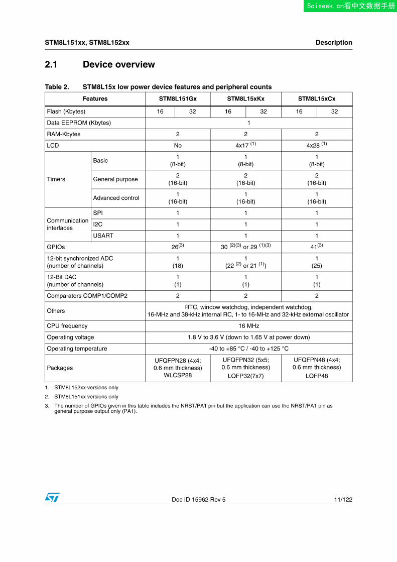
All devices offer 12-bit ADC, DAC, two comparators, Real-time clock three 16-bit timers, one 8-bit timer as well as standard communication interface such as SPI, I2C and USART. A 4x28-segment LCD is available on the STM8L152xx line. Table 2: STM8L15x low power device features and peripheral counts and Section 3 on page 13 give an overview of the complete range of peripherals proposed in this family.
The STM8L15xxx microcontroller family is suitable for a wide range of applications:
● Medical and handheld equipment
● Application control and user interface
● PC peripherals, gaming, GPS and sport equipment
● Alarm systems, wired and wireless sensors
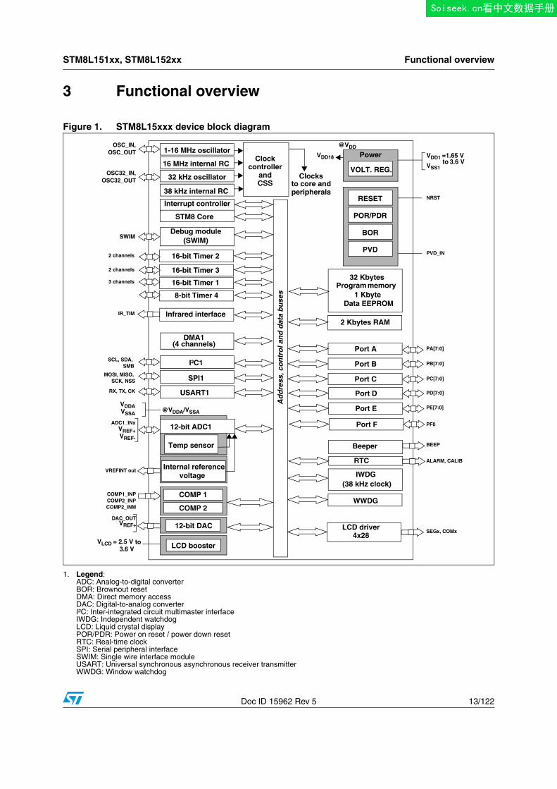
Figure 1 on page 13 shows the general block diagram of the device family.
Soiseek.cn看中文数据手册
Description STM8L151xx, STM8L152xx
10/122 Doc ID 15962 Rev 5
2 Description
The STM8L15xxx devices are members of the STM8L Ultralow power 8-bit family. The STM8L15xxx family operates from 1.8 V to 3.6 V (down to 1.65 V at power down) and is available in the -40 to +85 °C and -40 to +125 °C temperature ranges.
The STM8L15xxx Ultralow power family features the enhanced STM8 CPU core providing increased processing power (up to 16 MIPS at 16 MHz) while maintaining the advantages of a CISC architecture with improved code density, a 24-bit linear addressing space and an optimized architecture for low power operations.
The family includes an integrated debug module with a hardware interface (SWIM) which allows non-intrusive In-Application debugging and ultrafast Flash programming.
All STM8L15xxx microcontrollers feature embedded data EEPROM and low power low-voltage single-supply program Flash memory.
They incorporate an extensive range of enhanced I/Os and peripherals.
The modular design of the peripheral set allows the same peripherals to be found in different ST microcontroller families including 32-bit families. This makes any transition to a different family very easy, and simplified even more by the use of a common set of development tools.
Six different packages are proposed from 28 to 48 pins. Depending on the device chosen, different sets of peripherals are included. .
All STM8L Ultralow power products are based on the same architecture with the same memory mapping and a coherent pinout.
Soiseek.cn看中文数据手册
STM8L151xx, STM8L152xx Description
Doc ID 15962 Rev 5 11/122
2.1 Device overview
Table 2. STM8L15x low power device features and peripheral counts
Features STM8L151Gx STM8L15xKx STM8L15xCx
Flash (Kbytes) 16 32 16 32 16 32
Data EEPROM (Kbytes) 1
RAM-Kbytes 2 2 2
LCD No 4x17 (1) 4x28 (1)
Timers
Basic1
(8-bit)1
(8-bit)1
(8-bit)
General purpose2
(16-bit) 2
(16-bit) 2
(16-bit)
Advanced control1
(16-bit)1
(16-bit)1
(16-bit)
Communication interfaces
SPI 1 1 1
I2C 1 1 1
USART 1 1 1
GPIOs 26(3) 30 (2)(3) or 29 (1)(3) 41(3)
12-bit synchronized ADC(number of channels)
1 (18)
1(22 (2) or 21 (1))
1 (25)
12-Bit DAC(number of channels)
1(1)
1(1)
1(1)
Comparators COMP1/COMP2 2 2 2
OthersRTC, window watchdog, independent watchdog,
16-MHz and 38-kHz internal RC, 1- to 16-MHz and 32-kHz external oscillator
CPU frequency 16 MHz
Operating voltage 1.8 V to 3.6 V (down to 1.65 V at power down)
Operating temperature -40 to +85 °C / -40 to +125 °C
PackagesUFQFPN28 (4x4; 0.6 mm thickness)
WLCSP28
UFQFPN32 (5x5; 0.6 mm thickness)
LQFP32(7x7)
UFQFPN48 (4x4; 0.6 mm thickness)
LQFP48
1. STM8L152xx versions only
2. STM8L151xx versions only
3. The number of GPIOs given in this table includes the NRST/PA1 pin but the application can use the NRST/PA1 pin as general purpose output only (PA1).
Soiseek.cn看中文数据手册
Description STM8L151xx, STM8L152xx
12/122 Doc ID 15962 Rev 5
2.2 Ultralow power continuumThe Ultralow power STM8L151xx and STM8L152xx are fully pin-to-pin, software and feature compatible. Besides the full compatibility within the family, the devices are part of STMicroelectronics microcontrollers UtraLowPower strategy which also includes STM8L101xx and STM32L15xxx. The STM8L and STM32L families allow a continuum of performance, peripherals, system architecture, and features.
They are all based on STMicroelectronics 0.13 µm ultralow leakage process.
Note: 1 The STM8L151xx and STM8L152xx are pin-to-pin compatible with STM8L101xx devices.
2 The STM32L family is pin-to-pin compatible with the general purpose STM32F family. Please refer to STM32L15x documentation for more information on these devices.
Performance
All families incorporate highly energy-efficient cores with both Harvard architecture and pipelined execution: advanced STM8 core for STM8L families and ARM Cortex™-M3 core for STM32L family. In addition specific care for the design architecture has been taken to optimize the mA/DMIPS and mA/MHz ratios.
This allows the Ultralow power performance to range from 5 up to 33.3 DMIPs.
Shared peripherals
STM8L151xx/152xx and STM32L15xx share identical peripherals which ensure a very easy migration from one family to another:
● Analog peripherals: ADC1, DAC, and comparators COMP1/COMP2
● Digital peripherals: RTC and some communication interfaces
Common system strategy
To offer flexibility and optimize performance, the STM8L151xx/152xx and STM32L15xx devices use a common architecture:
● Same power supply range from 1.8 to 3.6 V, down to 1.65 V at power down
● Architecture optimized to reach ultralow consumption both in low power modes and Run mode
● Fast startup strategy from low power modes
● Flexible system clock
● Ultrasafe reset: same reset strategy for both STM8L15xxx and STM32L15xxx including power-on reset, power-down reset, brownout reset and programmable voltage detector.
Features
ST UtraLowPower continuum also lies in feature compatibility:
● More than 10 packages with pin count from 20 to 100 pins and size down to 3 x 3 mm
● Memory density ranging from 4 to 128 Kbytes
Soiseek.cn看中文数据手册
STM8L151xx, STM8L152xx Functional overview
Doc ID 15962 Rev 5 13/122
3 Functional overview
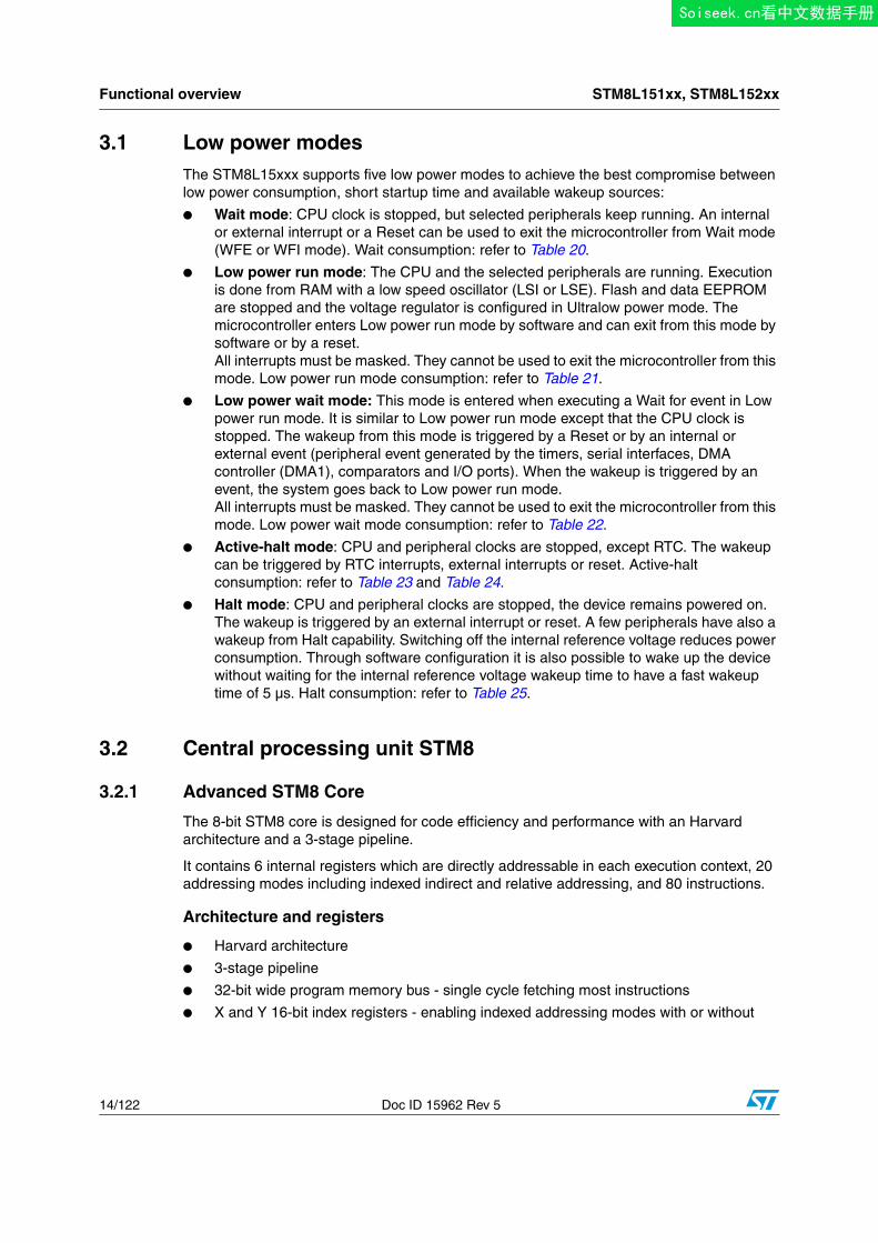
Figure 1. STM8L15xxx device block diagram
1. Legend:ADC: Analog-to-digital converterBOR: Brownout resetDMA: Direct memory accessDAC: Digital-to-analog converterI²C: Inter-integrated circuit multimaster interfaceIWDG: Independent watchdogLCD: Liquid crystal display POR/PDR: Power on reset / power down resetRTC: Real-time clockSPI: Serial peripheral interfaceSWIM: Single wire interface moduleUSART: Universal synchronous asynchronous receiver transmitterWWDG: Window watchdog
16 MHz internal RC Clock
Clocks
Ad
dre
ss, c
on
tro
l an
d d
ata
bu
ses
Debug module
SPI1
32 Kbytes
Interrupt controller
2 Kbytes RAM
to core andperipherals
IWDG (38 kHz clock)
(SWIM)
Port A
Port B
Port C
I²C1
USART1
Power
VOLT. REG.
Port F
1-16 MHz oscillator
32 kHz oscillator
38 kHz internal RC
LCD driver4x28
WWDG
STM8 Core
controllerandCSS
1 Kbyte
Port D
Port E
Beeper
RTC
memoryProgram
Data EEPROM
@VDD
VDD18 VDD1 =1.65 V
VSS1
SWIM
SCL, SDA,
MOSI, MISO, SCK, NSS
RX, TX, CK
ADC1_INx
DAC_OUT
COMP1_INP COMP 1
COMP 2COMP2_INP
VDDAVSSA
SMB
@VDDA/VSSA
Temp sensor
12-bit ADC1VREF+VREF-
3.6 V
12-bit DAC12-bit DAC
NRST
PA[7:0]
PB[7:0]
PC[7:0]
PD[7:0]
PE[7:0]
PF0
BEEP
ALARM, CALIB
SEGx, COMx
POR/PDR
OSC_IN,OSC_OUT
OSC32_IN,OSC32_OUT
to
BOR
PVD PVD_IN
RESET
DMA1
8-bit Timer 4
16-bit Timer 3
16-bit Timer 2
16-bit Timer 1
(4 channels)
2 channels
2 channels
3 channels
COMP2_INM
VLCD = 2.5 V3.6 V
to LCD booster
Internal reference voltage
VREFINT out
VREF+
Infrared interfaceIR_TIM
Soiseek.cn看中文数据手册
Functional overview STM8L151xx, STM8L152xx
14/122 Doc ID 15962 Rev 5
3.1 Low power modesThe STM8L15xxx supports five low power modes to achieve the best compromise between low power consumption, short startup time and available wakeup sources:
● Wait mode: CPU clock is stopped, but selected peripherals keep running. An internal or external interrupt or a Reset can be used to exit the microcontroller from Wait mode (WFE or WFI mode). Wait consumption: refer to Table 20.
● Low power run mode: The CPU and the selected peripherals are running. Execution is done from RAM with a low speed oscillator (LSI or LSE). Flash and data EEPROM are stopped and the voltage regulator is configured in Ultralow power mode. The microcontroller enters Low power run mode by software and can exit from this mode by software or by a reset. All interrupts must be masked. They cannot be used to exit the microcontroller from this mode. Low power run mode consumption: refer to Table 21.
● Low power wait mode: This mode is entered when executing a Wait for event in Low power run mode. It is similar to Low power run mode except that the CPU clock is stopped. The wakeup from this mode is triggered by a Reset or by an internal or external event (peripheral event generated by the timers, serial interfaces, DMA controller (DMA1), comparators and I/O ports). When the wakeup is triggered by an event, the system goes back to Low power run mode. All interrupts must be masked. They cannot be used to exit the microcontroller from this mode. Low power wait mode consumption: refer to Table 22.
● Active-halt mode: CPU and peripheral clocks are stopped, except RTC. The wakeup can be triggered by RTC interrupts, external interrupts or reset. Active-halt consumption: refer to Table 23 and Table 24.
● Halt mode: CPU and peripheral clocks are stopped, the device remains powered on. The wakeup is triggered by an external interrupt or reset. A few peripherals have also a wakeup from Halt capability. Switching off the internal reference voltage reduces power consumption. Through software configuration it is also possible to wake up the device without waiting for the internal reference voltage wakeup time to have a fast wakeup time of 5 µs. Halt consumption: refer to Table 25.
3.2 Central processing unit STM8
3.2.1 Advanced STM8 Core
The 8-bit STM8 core is designed for code efficiency and performance with an Harvard architecture and a 3-stage pipeline.
It contains 6 internal registers which are directly addressable in each execution context, 20 addressing modes including indexed indirect and relative addressing, and 80 instructions.
Architecture and registers
● Harvard architecture
● 3-stage pipeline
● 32-bit wide program memory bus - single cycle fetching most instructions
● X and Y 16-bit index registers - enabling indexed addressing modes with or without
Soiseek.cn看中文数据手册
STM8L151xx, STM8L152xx Functional overview
Doc ID 15962 Rev 5 15/122
offset and read-modify-write type data manipulations
● 8-bit accumulator
● 24-bit program counter - 16 Mbyte linear memory space
● 16-bit stack pointer - access to a 64 Kbyte level stack
● 8-bit condition code register - 7 condition flags for the result of the last instruction
Addressing
● 20 addressing modes
● Indexed indirect addressing mode for lookup tables located anywhere in the address space
● Stack pointer relative addressing mode for local variables and parameter passing
Instruction set
● 80 instructions with 2-byte average instruction size
● Standard data movement and logic/arithmetic functions
● 8-bit by 8-bit multiplication
● 16-bit by 8-bit and 16-bit by 16-bit division
● Bit manipulation
● Data transfer between stack and accumulator (push/pop) with direct stack access
● Data transfer using the X and Y registers or direct memory-to-memory transfers
3.2.2 Interrupt controller
The STM8L15xxx features a nested vectored interrupt controller:
● Nested interrupts with 3 software priority levels
● 32 interrupt vectors with hardware priority
● Up to 40 external interrupt sources on 11 vectors
● Trap and reset interrupts
Soiseek.cn看中文数据手册
Functional overview STM8L151xx, STM8L152xx
16/122 Doc ID 15962 Rev 5
3.3 Reset and supply management
3.3.1 Power supply scheme
The device requires a 1.65 V to 3.6 V operating supply voltage (VDD). The external power supply pins must be connected as follows:
● VSS1 ; VDD1 = 1.8 to 3.6 V, down to 1.65 V at power down: external power supply for I/Os and for the internal regulator. Provided externally through VDD1 pins, the corresponding ground pin is VSS1.
● VSSA ; VDDA = 1.8 to 3.6 V, down to 1.65 V at power down: external power supplies for analog peripherals (minimum voltage to be applied to VDDA is 1.8 V when the ADC1 is used). VDDA and VSSA must be connected to VDD1 and VSS1, respectively.
● VSS2 ; VDD2 = 1.8 to 3.6 V, down to 1.65 V at power down: external power supplies for I/Os. VDD2 and VSS2 must be connected to VDD1 and VSS1, respectively.
● VREF+ ; VREF- (for ADC1): external reference voltage for ADC1. Must be provided externally through VREF+ and VREF- pin.
● VREF+ (for DAC): external voltage reference for DAC must be provided externally through VREF+.
3.3.2 Power supply supervisor
The device has an integrated ZEROPOWER power-on reset (POR)/power-down reset (PDR), coupled with a brownout reset (BOR) circuitry. At power-on, BOR is always active, and ensures proper operation starting from 1.8 V. After the 1.8 V BOR threshold is reached, the option byte loading process starts, either to confirm or modify default thresholds, or to disable BOR permanently (in which case, the VDD min value at power down is 1.65 V).
Five BOR thresholds are available through option bytes, starting from 1.8 V to 3 V. To reduce the power consumption in Halt mode, it is possible to automatically switch off the internal reference voltage (and consequently the BOR) in Halt mode. The device remains under reset when VDD is below a specified threshold, VPOR/PDR or VBOR, without the need for any external reset circuit.
The device features an embedded programmable voltage detector (PVD) that monitors the VDD/VDDA power supply and compares it to the VPVD threshold. This PVD offers 7 different levels between 1.85 V and 3.05 V, chosen by software, with a step around 200 mV. An interrupt can be generated when VDD/VDDA drops below the VPVD threshold and/or when VDD/VDDA is higher than the VPVD threshold. The interrupt service routine can then generate a warning message and/or put the MCU into a safe state. The PVD is enabled by software.
3.3.3 Voltage regulator
The STM8L15xxx embeds an internal voltage regulator for generating the 1.8 V power supply for the core and peripherals.
This regulator has two different modes:
● Main voltage regulator mode (MVR) for Run, Wait for interrupt (WFI) and Wait for event (WFE) modes.
● Low power voltage regulator mode (LPVR) for Halt, Active-halt, Low power run and Low power wait modes.
Soiseek.cn看中文数据手册
STM8L151xx, STM8L152xx Functional overview
Doc ID 15962 Rev 5 17/122
When entering Halt or Active-halt modes, the system automatically switches from the MVR to the LPVR in order to reduce current consumption.
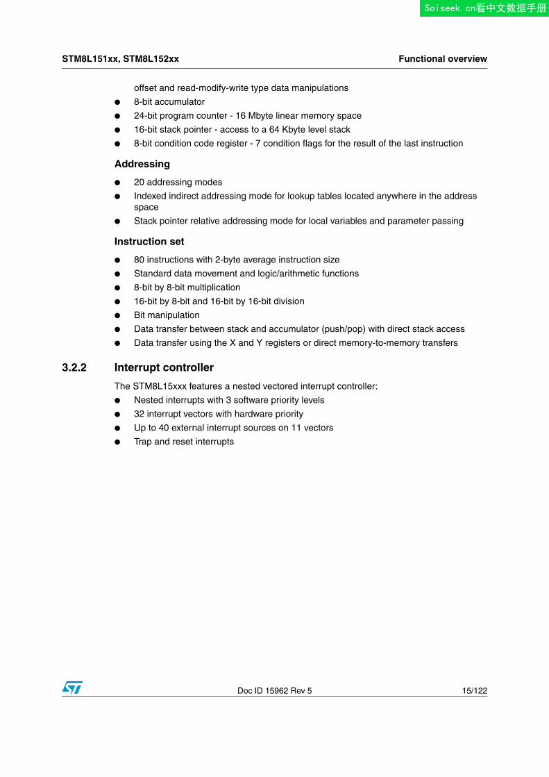
3.4 Clock managementThe clock controller distributes the system clock (SYSCLK) coming from different oscillators to the core and the peripherals. It also manages clock gating for low power modes and ensures clock robustness.
Features
● Clock prescaler: to get the best compromise between speed and current consumption the clock frequency to the CPU and peripherals can be adjusted by a programmable prescaler
● Safe clock switching: Clock sources can be changed safely on the fly in run mode through a configuration register.
● Clock management: To reduce power consumption, the clock controller can stop the clock to the core, individual peripherals or memory.
● System clock sources: 4 different clock sources can be used to drive the system clock:
– 1-16 MHz High speed external crystal (HSE)
– 16 MHz High speed internal RC oscillator (HSI)
– 32.768 Low speed external crystal (LSE)
– 38 kHz Low speed internal RC (LSI)
● RTC and LCD clock sources: the above four sources can be chosen to clock the RTC and the LCD, whatever the system clock.
● Startup clock: After reset, the microcontroller restarts by default with an internal 2 MHz clock (HSI/8). The prescaler ratio and clock source can be changed by the application program as soon as the code execution starts.
● Clock security system (CSS): This feature can be enabled by software. If a HSE clock failure occurs, the system clock is automatically switched to HSI.
● Configurable main clock output (CCO): This outputs an external clock for use by the application.
Soiseek.cn看中文数据手册
Functional overview STM8L151xx, STM8L152xx
18/122 Doc ID 15962 Rev 5
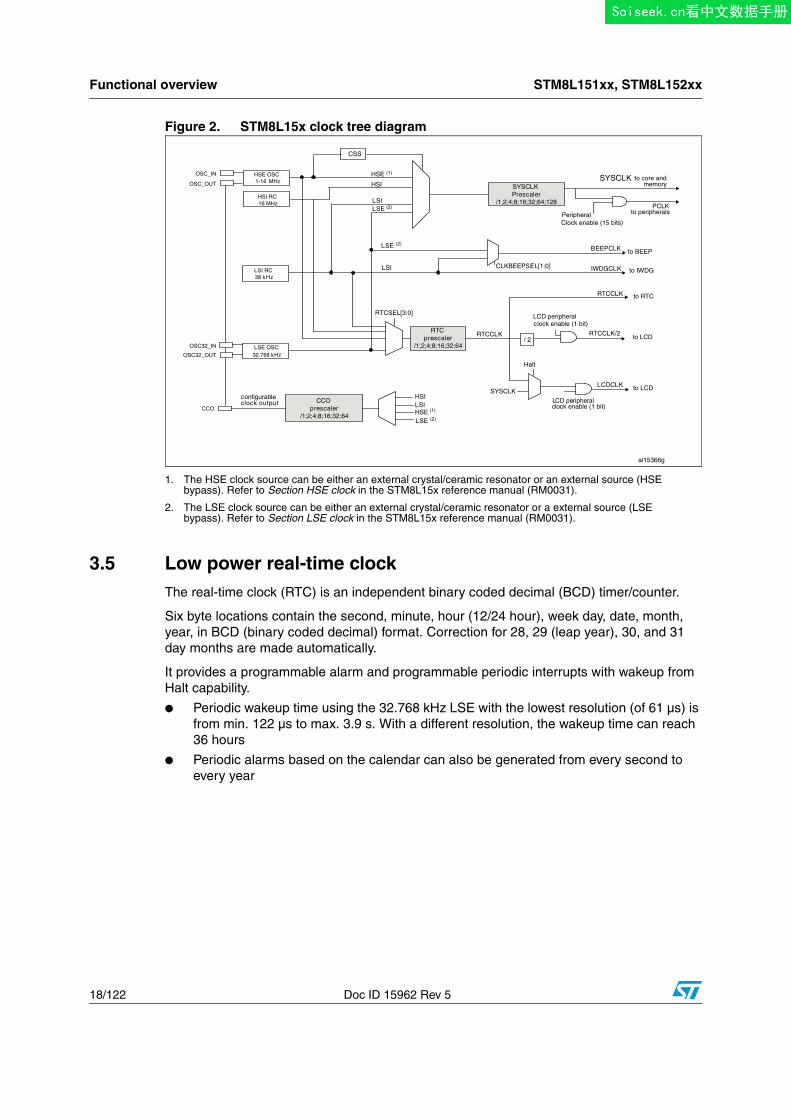
Figure 2. STM8L15x clock tree diagram
1. The HSE clock source can be either an external crystal/ceramic resonator or an external source (HSE bypass). Refer to Section HSE clock in the STM8L15x reference manual (RM0031).
2. The LSE clock source can be either an external crystal/ceramic resonator or a external source (LSE bypass). Refer to Section LSE clock in the STM8L15x reference manual (RM0031).
3.5 Low power real-time clock The real-time clock (RTC) is an independent binary coded decimal (BCD) timer/counter.
Six byte locations contain the second, minute, hour (12/24 hour), week day, date, month, year, in BCD (binary coded decimal) format. Correction for 28, 29 (leap year), 30, and 31 day months are made automatically.
It provides a programmable alarm and programmable periodic interrupts with wakeup from Halt capability.
● Periodic wakeup time using the 32.768 kHz LSE with the lowest resolution (of 61 µs) is from min. 122 µs to max. 3.9 s. With a different resolution, the wakeup time can reach 36 hours
● Periodic alarms based on the calendar can also be generated from every second to every year
Soiseek.cn看中文数据手册
STM8L151xx, STM8L152xx Functional overview
Doc ID 15962 Rev 5 19/122
3.6 LCD (Liquid crystal display)The liquid crystal display drives up to 4 common terminals and up to 28 segment terminals to drive up to 112 pixels.
● Internal step-up converter to guarantee contrast control whatever VDD.
● Static 1/2, 1/3, 1/4 duty supported.
● Static 1/2, 1/3 bias supported.
● Phase inversion to reduce power consumption and EMI.
● Up to 4 pixels which can programmed to blink.
● The LCD controller can operate in Halt mode.
Note: Unnecessary segments and common pins can be used as general I/O pins.
3.7 MemoriesThe STM8L15xxx devices have the following main features:
● Up to 2 Kbytes of RAM
● The non-volatile memory is divided into three arrays:
– Up to 32 Kbytes of medium-density embedded Flash program memory
– 1 Kbyte of Data EEPROM
– Option bytes.
The EEPROM embeds the error correction code (ECC) feature. It supports the read-while-write (RWW): it is possible to execute the code from the program matrix while programming/erasing the data matrix.
The option byte protects part of the Flash program memory from write and readout piracy.
3.8 DMAA 4-channel direct memory access controller (DMA1) offers a memory-to-memory and peripherals-from/to-memory transfer capability. The 4 channels are shared between the following IPs with DMA capability: ADC1, DAC, I2C1, SPI1, USART1, the 4 Timers.
3.9 Analog-to-digital converter ● 12-bit analog-to-digital converter (ADC1) with 25 channels (including 1 fast channel),
temperature sensor and internal reference voltage
● Conversion time down to 1 µs with fSYSCLK= 16 MHz
● Programmable resolution
● Programmable sampling time
● Single and continuous mode of conversion
● Scan capability: automatic conversion performed on a selected group of analog inputs
● Analog watchdog
● Triggered by timer
Note: ADC1 can be served by DMA1.
Soiseek.cn看中文数据手册
Functional overview STM8L151xx, STM8L152xx
20/122 Doc ID 15962 Rev 5
3.10 Digital-to-analog converter (DAC)● 12-bit DAC with output buffer
● Synchronized update capability using TIM4
● DMA capability
● External triggers for conversion
● Input reference voltage VREF+ for better resolution
Note: DAC can be served by DMA1.
3.11 Ultralow power comparatorsThe STM8L15x embeds two comparators (COMP1 and COMP2) sharing the same current bias and voltage reference. The voltage reference can be internal or external (coming from an I/O).
● One comparator with fixed threshold (COMP1).
● One comparator rail to rail with fast or slow mode (COMP2). The threshold can be one of the following:
– DAC output
– External I/O
– Internal reference voltage or internal reference voltage submultiple (1/4, 1/2, 3/4)
The two comparators can be used together to offer a window function. They can wake up from Halt mode.
3.12 System configuration controller and routing interfaceThe system configuration controller provides the capability to remap some alternate functions on different I/O ports. TIM4 and ADC1 DMA channels can also be remapped.
The highly flexible routing interface allows application software to control the routing of different I/Os to the TIM1 timer input captures. It also controls the routing of internal analog signals to ADC1, COMP1, COMP2, DAC and the internal reference voltage VREFINT. Finally, it provides a set of registers for efficiently managing a set of dedicated I/Os supporting up to 16 capacitive sensing channels using the ProxSenseTM technology.
3.13 TimersSTM8L15xxx devices contain one advanced control timer (TIM1), two 16-bit general purpose timers (TIM2 and TIM3) and one 8-bit basic timer (TIM4).
All the timers can be served by DMA1.
Table 3 compares the features of the advanced control, general-purpose and basic timers.
Soiseek.cn看中文数据手册
STM8L151xx, STM8L152xx Functional overview
Doc ID 15962 Rev 5 21/122
3.13.1 TIM1 - 16-bit advanced control timer
This is a high-end timer designed for a wide range of control applications. With its complementary outputs, dead-time control and center-aligned PWM capability, the field of applications is extended to motor control, lighting and half-bridge driver.
● 16-bit up, down and up/down autoreload counter with 16-bit prescaler
● 3 independent capture/compare channels (CAPCOM) configurable as input capture, output compare, PWM generation (edge and center aligned mode) and single pulse mode output
● 1 additional capture/compare channel which is not connected to an external I/O
● Synchronization module to control the timer with external signals
● Break input to force timer outputs into a defined state
● 3 complementary outputs with adjustable dead time
● Encoder mode
● Interrupt capability on various events (capture, compare, overflow, break, trigger)
3.13.2 16-bit general purpose timers
● 16-bit autoreload (AR) up/down-counter
● 7-bit prescaler adjustable to fixed power of 2 ratios (1…128)
● 2 individually configurable capture/compare channels
● PWM mode
● Interrupt capability on various events (capture, compare, overflow, break, trigger)
● Synchronization with other timers or external signals (external clock, reset, trigger and enable)
3.13.3 8-bit basic timer
The 8-bit timer consists of an 8-bit up auto-reload counter driven by a programmable prescaler. It can be used for timebase generation with interrupt generation on timer overflow or for DAC trigger generation.
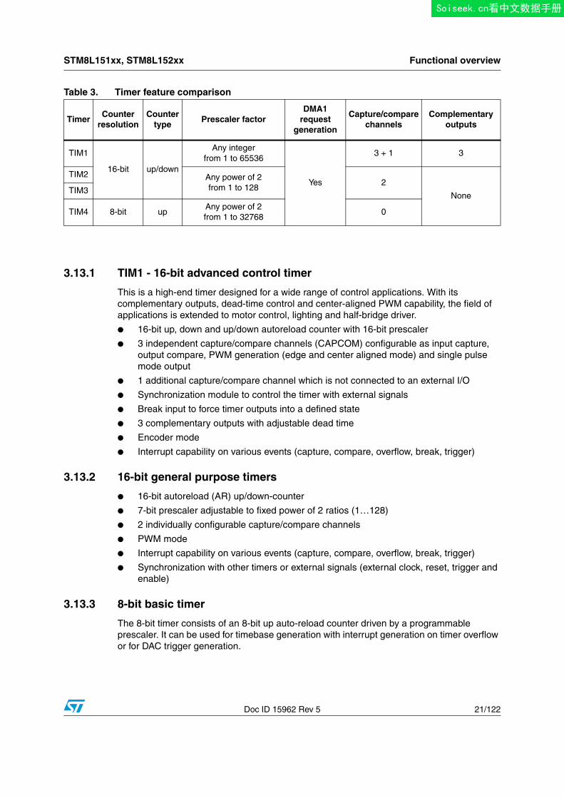
Table 3. Timer feature comparison
TimerCounter
resolutionCounter
typePrescaler factor
DMA1 request
generation
Capture/comparechannels
Complementaryoutputs
TIM1
16-bit up/down
Any integer from 1 to 65536
Yes
3 + 1 3
TIM2 Any power of 2 from 1 to 128
2
NoneTIM3
TIM4 8-bit upAny power of 2 from 1 to 32768
0
Soiseek.cn看中文数据手册
Functional overview STM8L151xx, STM8L152xx
22/122 Doc ID 15962 Rev 5
3.14 Watchdog timersThe watchdog system is based on two independent timers providing maximum security to the applications.
3.14.1 Window watchdog timer
The window watchdog (WWDG) is used to detect the occurrence of a software fault, usually generated by external interferences or by unexpected logical conditions, which cause the application program to abandon its normal sequence.
3.14.2 Independent watchdog timer
The independent watchdog peripheral (IWDG) can be used to resolve processor malfunctions due to hardware or software failures.
It is clocked by the internal LSI RC clock source, and thus stays active even in case of a CPU clock failure.
3.15 BeeperThe beeper function outputs a signal on the BEEP pin for sound generation. The signal is in the range of 1, 2 or 4 kHz.
3.16 Communication interfaces
3.16.1 SPI
The serial peripheral interface (SPI1) provides half/ full duplex synchronous serial communication with external devices.
● Maximum speed: 8 Mbit/s (fSYSCLK/2) both for master and slave
● Full duplex synchronous transfers
● Simplex synchronous transfers on 2 lines with a possible bidirectional data line
● Master or slave operation - selectable by hardware or software
● Hardware CRC calculation
● Slave/master selection input pin
Note: SPI1 can be served by the DMA1 Controller.
3.16.2 I²C
The I2C bus interface (I2C1) provides multi-master capability, and controls all I²C bus-specific sequencing, protocol, arbitration and timing.
● Master, slave and multi-master capability
● Standard mode up to 100 kHz and fast speed modes up to 400 kHz.
● 7-bit and 10-bit addressing modes.
● SMBus 2.0 and PMBus support
● Hardware CRC calculation
Soiseek.cn看中文数据手册
STM8L151xx, STM8L152xx Functional overview
Doc ID 15962 Rev 5 23/122
Note: I2C1 can be served by the DMA1 Controller.
3.16.3 USART
The USART interface (USART1) allows full duplex, asynchronous communications with external devices requiring an industry standard NRZ asynchronous serial data format. It offers a very wide range of baud rates.
● 1 Mbit/s full duplex SCI
● SPI1 emulation
● High precision baud rate generator
● Smartcard emulation
● IrDA SIR encoder decoder
● Single wire half duplex mode
Note: USART1 can be served by the DMA1 Controller.
3.17 Infrared (IR) interfaceThe STM8L15x devices contain an infrared interface which can be used with an IR LED for remote control functions. Two timer output compare channels are used to generate the infrared remote control signals.
3.18 Development support
Development tools
Development tools for the STM8 microcontrollers include:
● The STice emulation system offering tracing and code profiling
● The STVD high-level language debugger including C compiler, assembler and integrated development environment
● The STVP Flash programming software
The STM8 also comes with starter kits, evaluation boards and low-cost in-circuit debugging/programming tools.
Single wire data interface (SWIM) and debug module
The debug module with its single wire data interface (SWIM) permits non-intrusive real-time in-circuit debugging and fast memory programming.
The Single wire interface is used for direct access to the debugging module and memory programming. The interface can be activated in all device operation modes.
The non-intrusive debugging module features a performance close to a full-featured emulator. Beside memory and peripherals, CPU operation can also be monitored in real-time by means of shadow registers.
Bootloader
A bootloader is available to reprogram the Flash memory using the USART1 interface.
Soiseek.cn看中文数据手册
Pin description STM8L151xx, STM8L152xx
24/122 Doc ID 15962 Rev 5
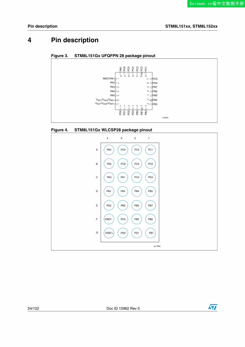
4 Pin description
Figure 3. STM8L151Gx UFQFPN 28 package pinout
Figure 4. STM8L151Gx WLCSP28 package pinoutPD3
PB0
PB1
PB2
PD0
PD1
PD2
PA5
VSS1/VSSA/VREF-VDD1/VDDA/VREF+
NRST/PA1PA2
PA4 PB6PB5
PB4
PB3
PC0
PD4PB7
PC4
PC3
PC2
PC1
PA0
PC6
PC5
2
1
3
4
5
6
798 10 11 12 13 14
20
21
19
18
17
16
15
2728 26 25 24 23 22
PA3
Soiseek.cn看中文数据手册
STM8L151xx, STM8L152xx Pin description
Doc ID 15962 Rev 5 25/122
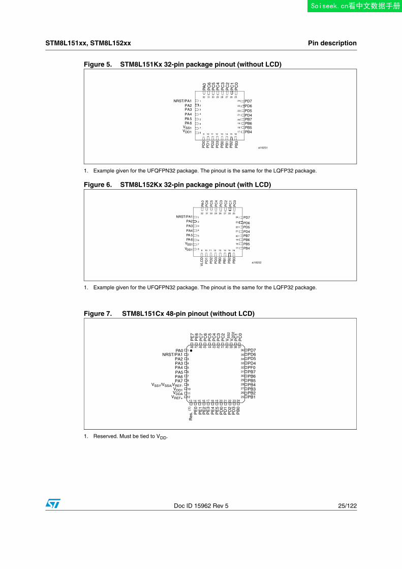
Figure 5. STM8L151Kx 32-pin package pinout (without LCD)
1. Example given for the UFQFPN32 package. The pinout is the same for the LQFP32 package.
Figure 6. STM8L152Kx 32-pin package pinout (with LCD)
1. Example given for the UFQFPN32 package. The pinout is the same for the LQFP32 package.
Figure 7. STM8L151Cx 48-pin pinout (without LCD)
1. Reserved. Must be tied to VDD.
44 43 42 41 40 39 38 3736
35
34333231302928272625
242312
13 14 15 16 17 18 19 20 21 22
1
2
3
4
5
6 7 8 9 10
11
48 47 46 45
PA5
VSS1/VSSA/VREF-
NRST/PA1PA2PA3PA4
PA6
Res
. (1)
PE
0P
E1
PD
1P
D2
PD
3P
B0
PE
3
PD
0P
E5
PE
4
PA7
VDD1VDDA
VREF+
PE
2
PB1PB2
PC
0P
C1
VD
D2
VS
S2
PC
2P
C3
PC
4P
C5
PC
6P
C7
PE
6P
E7
PB3PB4PB5PB6PB7PF0PD4PD5PD6PD7PA0
Soiseek.cn看中文数据手册
Pin description STM8L151xx, STM8L152xx
26/122 Doc ID 15962 Rev 5
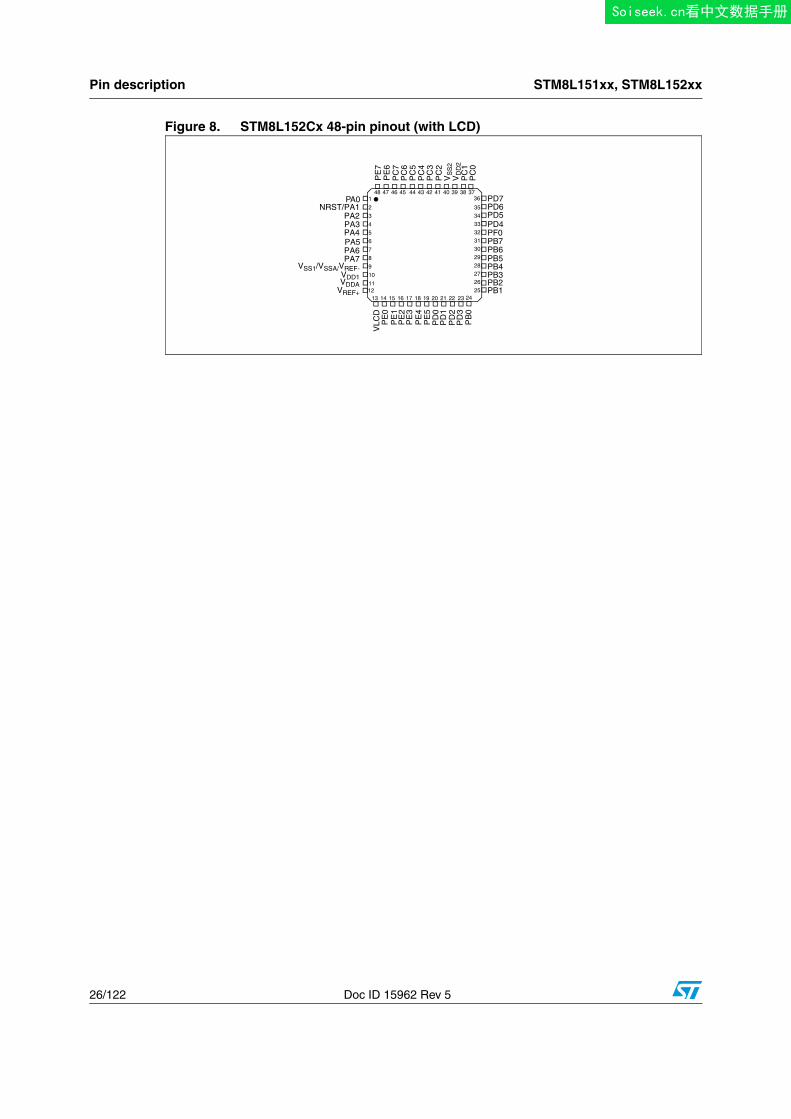
Figure 8. STM8L152Cx 48-pin pinout (with LCD)
44 43 42 41 40 39 38 3736
3534333231302928272625
242312
13 14 15 16 17 18 19 20 21 22
1
2
3
4
5
6 7 8 9 10
11
48 47 46 45
PA5
VSS1/VSSA/VREF-
NRST/PA1PA2PA3PA4
PA6
VLC
DP
E0
PE
1
PD
1P
D2
PD
3P
B0
PE
3
PD
0P
E5
PE
4
PA7
VDD1VDDA
VREF+
PE
2
PB1PB2
PC
0P
C1
VD
D2
VS
S2
PC
2P
C3
PC
4P
C5
PC
6P
C7
PE
6P
E7
PB3PB4PB5PB6PB7PF0PD4PD5PD6PD7PA0
Soiseek.cn看中文数据手册
STM8L151xx, STM8L152xx Pin description
Doc ID 15962 Rev 5 27/122
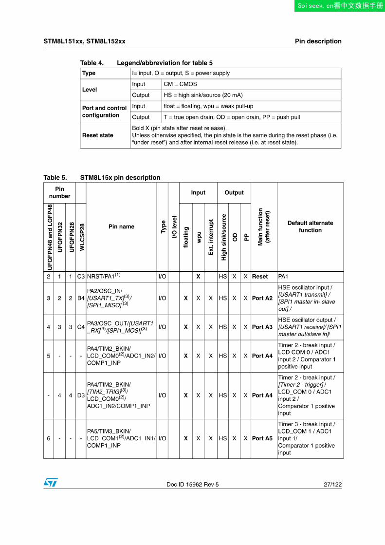
Table 4. Legend/abbreviation for table 5
Type I= input, O = output, S = power supply
LevelInput CM = CMOS
Output HS = high sink/source (20 mA)
Port and control configuration
Input float = floating, wpu = weak pull-up
Output T = true open drain, OD = open drain, PP = push pull
Reset stateBold X (pin state after reset release). Unless otherwise specified, the pin state is the same during the reset phase (i.e. “under reset”) and after internal reset release (i.e. at reset state).
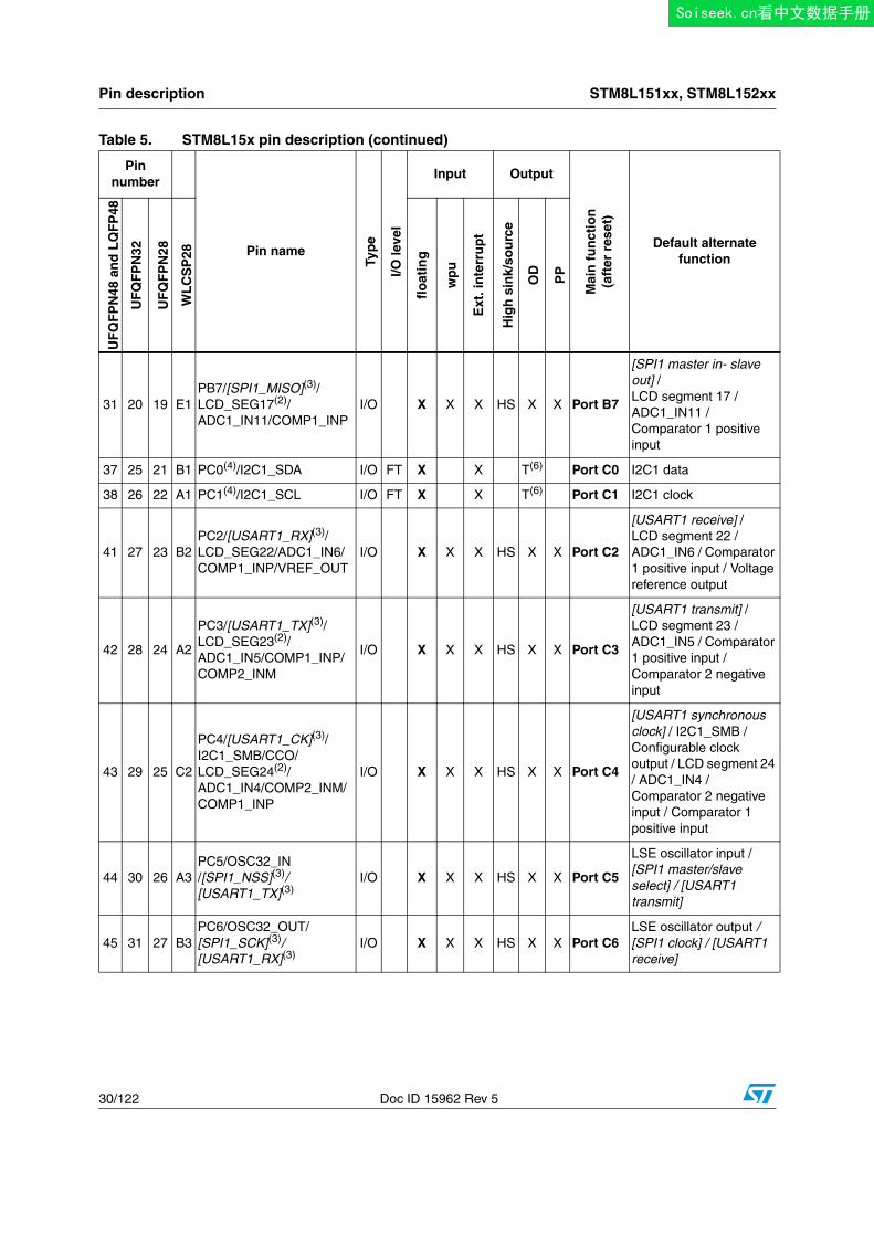
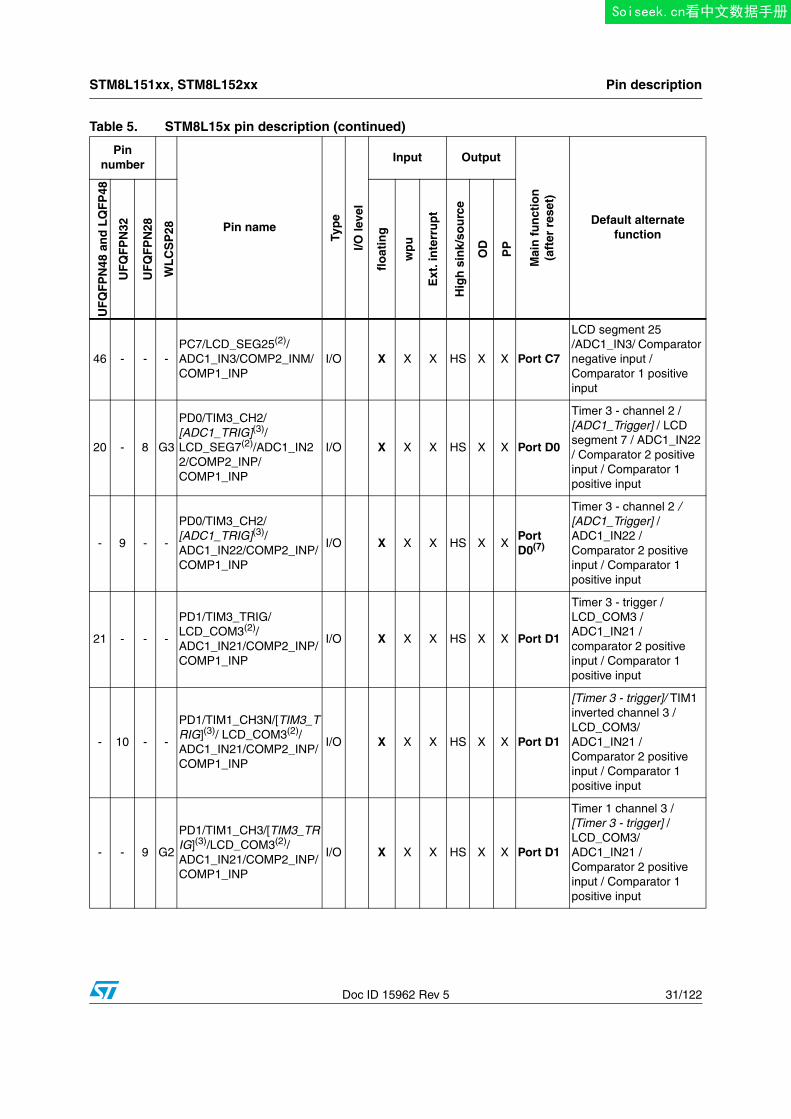
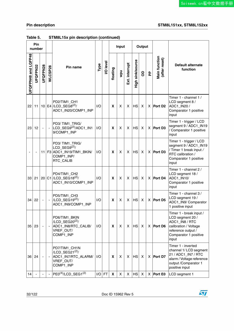
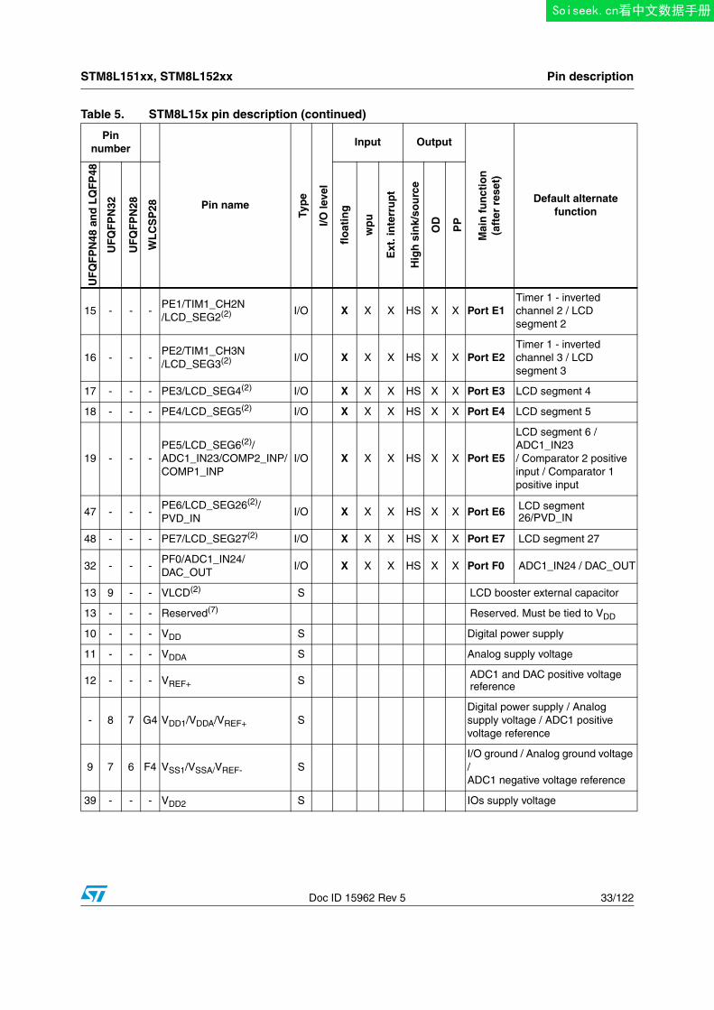
Table 5. STM8L15x pin description
Pin number
Pin name
Typ
e
I/O le
vel
Input Output
Mai
n f
un
ctio
n(a
fter
res
et)
Default alternate function
UF
QF
PN
48 a
nd
LQ
FP
48
UF
QF
PN
32
UF
QF
PN
28
WL
CS
P28
flo
atin
g
wp
u
Ext
. in
terr
up
t
Hig
h s
ink/
sou
rce
OD
PP
2 1 1 C3 NRST/PA1(1) I/O X HS X X Reset PA1
3 2 2 B4PA2/OSC_IN/[USART1_TX](3)/[SPI1_MISO] (3)
I/O X X X HS X X Port A2
HSE oscillator input / [USART1 transmit] / [SPI1 master in- slave out] /
4 3 3 C4PA3/OSC_OUT/[USART1_RX](3)/[SPI1_MOSI](3) I/O X X X HS X X Port A3
HSE oscillator output / [USART1 receive]/ [SPI1 master out/slave in]/
5 - - -PA4/TIM2_BKIN/LCD_COM0(2)/ADC1_IN2/COMP1_INP
I/O X X X HS X X Port A4
Timer 2 - break input / LCD COM 0 / ADC1 input 2 / Comparator 1 positive input
- 4 4 D3
PA4/TIM2_BKIN/[TIM2_TRIG](3)/LCD_COM0(2)/ADC1_IN2/COMP1_INP
I/O X X X HS X X Port A4
Timer 2 - break input /[Timer 2 - trigger] / LCD_COM 0 / ADC1 input 2 / Comparator 1 positive input
6 - - -PA5/TIM3_BKIN/LCD_COM1(2)/ADC1_IN1/COMP1_INP
I/O X X X HS X X Port A5
Timer 3 - break input /LCD_COM 1 / ADC1 input 1/Comparator 1 positive input
Soiseek.cn看中文数据手册
Pin description STM8L151xx, STM8L152xx
28/122 Doc ID 15962 Rev 5
- 5 5 D4
PA5/TIM3_BKIN/[TIM3_TRIG](3)/LCD_COM1(2)/ADC1_IN1/COMP1_INP
I/O X X X HS X X Port A5
Timer 3 - break input / [Timer 3 - trigger] / LCD_COM 1 / ADC1 input 1 /Comparator 1 positive input
7 6 - -PA6/[ADC1_TRIG](3)/LCD_COM2(2)/ADC1_IN0/COMP1_INP
I/O X X X HS X X Port A6
[ADC1 - trigger] / LCD_COM2 /ADC1 input 0 /Comparator 1 positive input
8 - - - PA7/LCD_SEG0(2)(4) I/O FT X X X HS X X Port A7 LCD segment 0
24 13 12 E3PB0(5)/TIM2_CH1/ LCD_SEG10(2)/ADC1_IN18/COMP1_INP
I/O X(5) X(5) X HS X X Port B0
Timer 2 - channel 1 / LCD segment 10 / ADC1_IN18 / Comparator 1 positive input
25 14 13 G1PB1/TIM3_CH1/LCD_SEG11(2)/ADC1_IN17/COMP1_INP
I/O X X X HS X X Port B1
Timer 3 - channel 1 / LCD segment 11 / ADC1_IN17 /Comparator 1 positive input
26 15 14 F2PB2/ TIM2_CH2/ LCD_SEG12(2)/ADC1_IN16/COMP1_INP
I/O X X X HS X X Port B2
Timer 2 - channel 2 / LCD segment 12 / ADC1_IN16/Comparator 1 positive input
27 - - -PB3/TIM2_TRIG/LCD_SEG13(2)/ADC1_IN15/COMP1_INP
I/O X X X HS X X Port B3
Timer 2 - trigger / LCD segment 13 /ADC1_IN15 / Comparator 1 positive input
- 16 - -
PB3/[TIM2_TRIG](3)/TIM1_CH2N/LCD_SEG13(2)/ADC1_IN15/COMP1_INP
I/O X X X HS X X Port B3
[Timer 2 - trigger] / Timer 1 inverted channel 2 / LCD segment 13 / ADC1_IN15 / Comparator 1 positive input
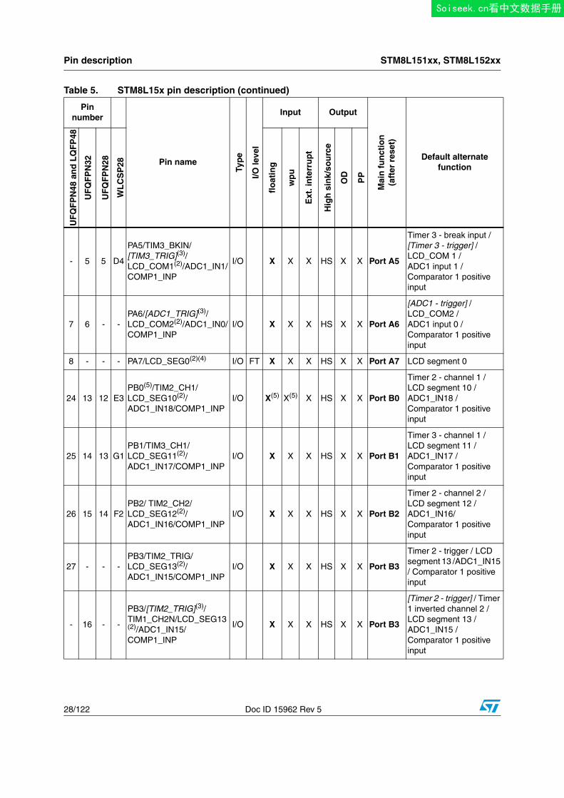
Table 5. STM8L15x pin description (continued)
Pin number
Pin name
Typ
e
I/O le
vel
Input Output
Mai
n f
un
ctio
n(a
fter
res
et)
Default alternate function
UF
QF
PN
48 a
nd
LQ
FP
48
UF
QF
PN
32
UF
QF
PN
28
WL
CS
P28
flo
atin
g
wp
u
Ext
. in
terr
up
t
Hig
h s
ink/
sou
rce
OD
PP
Soiseek.cn看中文数据手册
STM8L151xx, STM8L152xx Pin description
Doc ID 15962 Rev 5 29/122
- - 15 E2
PB3/[TIM2_TRIG](3)/TIM1_CH1N/LCD_SEG13(2)/ADC1_IN15/RTC_ALARM/COMP1_INP
I/O X X X HS X X Port B3
[Timer 2 - trigger] / Timer 1 inverted channel 1/ LCD segment 13 / ADC1_IN15 / RTC alarm/ Comparator 1 positive input
28 - - -PB4(5)/[SPI1_NSS](3)/LCD_SEG14(2)/ADC1_IN14/COMP1_INP
I/O X(5) X(5) X HS X X Port B4
[SPI1 master/slave select] / LCD segment 14 / ADC1_IN14 / Comparator 1 positive input
- 17 16 D2
PB4(5)/[SPI1_NSS](3)/LCD_SEG14(2)/ADC1_IN14/COMP1_INP/DAC_OUT
I/O X(5) X(5) X HS X X Port B4
[SPI1 master/slave select] / LCD segment 14 / ADC1_IN14 /DAC output / Comparator 1 positive input
29 - - -PB5/[SPI1_SCK](3)/LCD_SEG15(2)/ADC1_IN13/COMP1_INP
I/O X X X HS X X Port B5
[SPI1 clock] / LCD segment 15 / ADC1_IN13 / Comparator 1 positive input
- 18 17 D1
PB5/[SPI1_SCK](3)/LCD_SEG15(2)/ADC1_IN13/DAC_OUT/COMP1_INP
I/O X X X HS X X Port B5
[SPI1 clock] / LCD segment 15 / ADC1_IN13 / DAC output/Comparator 1 positive input
30 - - -PB6/[SPI1_MOSI](3)/LCD_SEG16(2)/ADC1_IN12/COMP1_INP
I/O X X X HS X X Port B6
[SPI1 master out/slave in]/LCD segment 16 / ADC1_IN12 / Comparator 1 positive input
- 19 18 F1
PB6/[SPI1_MOSI](3)/LCD_SEG16(2)/ADC1_IN12/COMP1_INP/DAC_OUT
I/O X X X HS X X Port B6
[SPI1 master out]/slave in / LCD segment 16 / ADC1_IN12 / DAC output / Comparator 1 positive input
Table 5. STM8L15x pin description (continued)
Pin number
Pin name
Typ
e
I/O le
vel
Input Output
Mai
n f
un
ctio
n(a
fter
res
et)
Default alternate function
UF
QF
PN
48 a
nd
LQ
FP
48
UF
QF
PN
32
UF
QF
PN
28
WL
CS
P28
flo
atin
g
wp
u
Ext
. in
terr
up
t
Hig
h s
ink/
sou
rce
OD
PP
Soiseek.cn看中文数据手册
Pin description STM8L151xx, STM8L152xx
30/122 Doc ID 15962 Rev 5
31 20 19 E1PB7/[SPI1_MISO](3)/LCD_SEG17(2)/ADC1_IN11/COMP1_INP
I/O X X X HS X X Port B7
[SPI1 master in- slave out] / LCD segment 17 / ADC1_IN11 / Comparator 1 positive input
37 25 21 B1 PC0(4)/I2C1_SDA I/O FT X X T(6) Port C0 I2C1 data
38 26 22 A1 PC1(4)/I2C1_SCL I/O FT X X T(6) Port C1 I2C1 clock
41 27 23 B2PC2/[USART1_RX](3)/LCD_SEG22/ADC1_IN6/COMP1_INP/VREF_OUT
I/O X X X HS X X Port C2
[USART1 receive] / LCD segment 22 / ADC1_IN6 / Comparator 1 positive input / Voltage reference output
42 28 24 A2
PC3/[USART1_TX](3)/LCD_SEG23(2)/ADC1_IN5/COMP1_INP/COMP2_INM
I/O X X X HS X X Port C3
[USART1 transmit] / LCD segment 23 / ADC1_IN5 / Comparator 1 positive input / Comparator 2 negative input
43 29 25 C2
PC4/[USART1_CK](3)/I2C1_SMB/CCO/LCD_SEG24(2)/ADC1_IN4/COMP2_INM/COMP1_INP
I/O X X X HS X X Port C4
[USART1 synchronous clock] / I2C1_SMB / Configurable clock output / LCD segment 24 / ADC1_IN4 / Comparator 2 negative input / Comparator 1 positive input
44 30 26 A3PC5/OSC32_IN /[SPI1_NSS](3)/[USART1_TX](3)
I/O X X X HS X X Port C5
LSE oscillator input / [SPI1 master/slave select] / [USART1 transmit]
45 31 27 B3PC6/OSC32_OUT/[SPI1_SCK](3)/[USART1_RX](3)
I/O X X X HS X X Port C6LSE oscillator output / [SPI1 clock] / [USART1 receive]
Table 5. STM8L15x pin description (continued)
Pin number
Pin name
Typ
e
I/O le
vel
Input Output
Mai
n f
un
ctio
n(a
fter
res
et)
Default alternate function
UF
QF
PN
48 a
nd
LQ
FP
48
UF
QF
PN
32
UF
QF
PN
28
WL
CS
P28
flo
atin
g
wp
u
Ext
. in
terr
up
t
Hig
h s
ink/
sou
rce
OD
PP
Soiseek.cn看中文数据手册
STM8L151xx, STM8L152xx Pin description
Doc ID 15962 Rev 5 31/122
46 - - -PC7/LCD_SEG25(2)/ADC1_IN3/COMP2_INM/COMP1_INP
I/O X X X HS X X Port C7
LCD segment 25 /ADC1_IN3/ Comparator negative input / Comparator 1 positive input
20 - 8 G3
PD0/TIM3_CH2/[ADC1_TRIG](3)/LCD_SEG7(2)/ADC1_IN22/COMP2_INP/COMP1_INP
I/O X X X HS X X Port D0
Timer 3 - channel 2 / [ADC1_Trigger] / LCD segment 7 / ADC1_IN22 / Comparator 2 positive input / Comparator 1 positive input
- 9 - -
PD0/TIM3_CH2/[ADC1_TRIG](3)/ADC1_IN22/COMP2_INP/COMP1_INP
I/O X X X HS X XPort D0(7)
Timer 3 - channel 2 / [ADC1_Trigger] / ADC1_IN22 / Comparator 2 positive input / Comparator 1 positive input
21 - - -
PD1/TIM3_TRIG/ LCD_COM3(2)/ADC1_IN21/COMP2_INP/COMP1_INP
I/O X X X HS X X Port D1
Timer 3 - trigger / LCD_COM3 / ADC1_IN21 / comparator 2 positive input / Comparator 1 positive input
- 10 - -
PD1/TIM1_CH3N/[TIM3_TRIG](3)/ LCD_COM3(2)/ADC1_IN21/COMP2_INP/COMP1_INP
I/O X X X HS X X Port D1
[Timer 3 - trigger]/ TIM1 inverted channel 3 / LCD_COM3/ADC1_IN21 / Comparator 2 positive input / Comparator 1 positive input
- - 9 G2
PD1/TIM1_CH3/[TIM3_TRIG](3)/LCD_COM3(2)/ADC1_IN21/COMP2_INP/COMP1_INP
I/O X X X HS X X Port D1
Timer 1 channel 3 / [Timer 3 - trigger] / LCD_COM3/ADC1_IN21 / Comparator 2 positive input / Comparator 1 positive input
Table 5. STM8L15x pin description (continued)
Pin number
Pin name
Typ
e
I/O le
vel
Input Output
Mai
n f
un
ctio
n(a
fter
res
et)
Default alternate function
UF
QF
PN
48 a
nd
LQ
FP
48
UF
QF
PN
32
UF
QF
PN
28
WL
CS
P28
flo
atin
g
wp
u
Ext
. in
terr
up
t
Hig
h s
ink/
sou
rce
OD
PP
Soiseek.cn看中文数据手册
Pin description STM8L151xx, STM8L152xx
32/122 Doc ID 15962 Rev 5
22 11 10 E4PD2/TIM1_CH1 /LCD_SEG8(2)/ADC1_IN20/COMP1_INP
I/O X X X HS X X Port D2
Timer 1 - channel 1 / LCD segment 8 / ADC1_IN20 / Comparator 1 positive input
23 12 - -PD3/ TIM1_TRIG/ LCD_SEG9(2)/ADC1_IN19/COMP1_INP
I/O X X X HS X X Port D3
Timer 1 - trigger / LCD segment 9 / ADC1_IN19 / Comparator 1 positive input
- - 11 F3
PD3/ TIM1_TRIG/ LCD_SEG9(2)/ADC1_IN19/TIM1_BKIN/COMP1_INP/RTC_CALIB
I/O X X X HS X X Port D3
Timer 1 - trigger / LCD segment 9 / ADC1_IN19 / Timer 1 break input / RTC calibration / Comparator 1 positive input
33 21 20 C1PD4/TIM1_CH2 /LCD_SEG18(2)/ADC1_IN10/COMP1_INP
I/O X X X HS X X Port D4
Timer 1 - channel 2 / LCD segment 18 / ADC1_IN10/ Comparator 1 positive input
34 22 - -PD5/TIM1_CH3 /LCD_SEG19(2)/ADC1_IN9/COMP1_INP
I/O X X X HS X X Port D5
Timer 1 - channel 3 / LCD segment 19 / ADC1_IN9/ Comparator 1 positive input
35 23 - -
PD6/TIM1_BKIN /LCD_SEG20(2)/ADC1_IN8/RTC_CALIB/VREF_OUT/COMP1_INP
I/O X X X HS X X Port D6
Timer 1 - break input / LCD segment 20 / ADC1_IN8 / RTC calibration / Voltage reference output / Comparator 1 positive input
36 24 - -
PD7/TIM1_CH1N /LCD_SEG21(2)/ADC1_IN7/RTC_ALARM/VREF_OUT/COMP1_INP
I/O X X X HS X X Port D7
Timer 1 - inverted channel 1/ LCD segment 21 / ADC1_IN7 / RTC alarm / Voltage reference output /Comparator 1 positive input
14 - - - PE0(4)/LCD_SEG1(2) I/O FT X X X HS X X Port E0 LCD segment 1
Table 5. STM8L15x pin description (continued)
Pin number
Pin name
Typ
e
I/O le
vel
Input Output
Mai
n f
un
ctio
n(a
fter
res
et)
Default alternate function
UF
QF
PN
48 a
nd
LQ
FP
48
UF
QF
PN
32
UF
QF
PN
28
WL
CS
P28
flo
atin
g
wp
u
Ext
. in
terr
up
t
Hig
h s
ink/
sou
rce
OD
PP
Soiseek.cn看中文数据手册
STM8L151xx, STM8L152xx Pin description
Doc ID 15962 Rev 5 33/122
15 - - -PE1/TIM1_CH2N /LCD_SEG2(2) I/O X X X HS X X Port E1
Timer 1 - inverted channel 2 / LCD segment 2
16 - - -PE2/TIM1_CH3N /LCD_SEG3(2) I/O X X X HS X X Port E2
Timer 1 - inverted channel 3 / LCD segment 3
17 - - - PE3/LCD_SEG4(2) I/O X X X HS X X Port E3 LCD segment 4
18 - - - PE4/LCD_SEG5(2) I/O X X X HS X X Port E4 LCD segment 5
19 - - -PE5/LCD_SEG6(2)/ADC1_IN23/COMP2_INP/COMP1_INP
I/O X X X HS X X Port E5
LCD segment 6 / ADC1_IN23/ Comparator 2 positive input / Comparator 1 positive input
47 - - -PE6/LCD_SEG26(2)/PVD_IN
I/O X X X HS X X Port E6 LCD segment 26/PVD_IN
48 - - - PE7/LCD_SEG27(2) I/O X X X HS X X Port E7 LCD segment 27
32 - - -PF0/ADC1_IN24/DAC_OUT
I/O X X X HS X X Port F0 ADC1_IN24 / DAC_OUT
13 9 - - VLCD(2) S LCD booster external capacitor
13 - - - Reserved(7) Reserved. Must be tied to VDD
10 - - - VDD S Digital power supply
11 - - - VDDA S Analog supply voltage
12 - - - VREF+ S ADC1 and DAC positive voltage reference
- 8 7 G4 VDD1/VDDA/VREF+ SDigital power supply / Analog supply voltage / ADC1 positive voltage reference
9 7 6 F4 VSS1/VSSA/VREF- SI/O ground / Analog ground voltage / ADC1 negative voltage reference
39 - - - VDD2 S IOs supply voltage
Table 5. STM8L15x pin description (continued)
Pin number
Pin name
Typ
e
I/O le
vel
Input Output
Mai
n f
un
ctio
n(a
fter
res
et)
Default alternate function
UF
QF
PN
48 a
nd
LQ
FP
48
UF
QF
PN
32
UF
QF
PN
28
WL
CS
P28
flo
atin
g
wp
u
Ext
. in
terr
up
t
Hig
h s
ink/
sou
rce
OD
PP
Soiseek.cn看中文数据手册
Pin description STM8L151xx, STM8L152xx
34/122 Doc ID 15962 Rev 5
4.1 System configuration optionsAs shown in Table 5: STM8L15x pin description, some alternate functions can be remapped on different I/O ports by programming one of the two remapping registers described in the “ Routing interface (RI) and system configuration controller” section in the STM8L15xxx reference manual (RM0031).
40 - - - VSS2 S IOs ground voltage
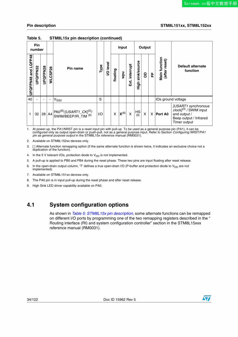
1 32 28 A4PA0(8)/[USART1_CK](3)/SWIM/BEEP/IR_TIM (9) I/O X X(8) X
HS(9) X X Port A0
[USART1 synchronous clock](3) / SWIM input and output /Beep output / Infrared Timer output
1. At power-up, the PA1/NRST pin is a reset input pin with pull-up. To be used as a general purpose pin (PA1), it can be configured only as output open-drain or push-pull, not as a general purpose input. Refer to Section Configuring NRST/PA1 pin as general purpose output in the STM8L15x reference manual (RM0031).
2. Available on STM8L152xx devices only.
3. [ ] Alternate function remapping option (if the same alternate function is shown twice, it indicates an exclusive choice not a duplication of the function).
4. In the 5 V tolerant I/Os, protection diode to VDD is not implemented.
5. A pull-up is applied to PB0 and PB4 during the reset phase. These two pins are input floating after reset release.
6. In the open-drain output column, ‘T’ defines a true open-drain I/O (P-buffer and protection diode to VDD are not implemented).
7. Available on STM8L151xx devices only.
8. The PA0 pin is in input pull-up during the reset phase and after reset release.
9. High Sink LED driver capability available on PA0.
Table 5. STM8L15x pin description (continued)
Pin number
Pin name
Typ
e
I/O le
vel
Input Output
Mai
n f
un
ctio
n(a
fter
res
et)
Default alternate function
UF
QF
PN
48 a
nd
LQ
FP
48
UF
QF
PN
32
UF
QF
PN
28
WL
CS
P28
flo
atin
g
wp
u
Ext
. in
terr
up
t
Hig
h s
ink/
sou
rce
OD
PP
Soiseek.cn看中文数据手册
STM8L151xx, STM8L152xx Memory and register map
Doc ID 15962 Rev 5 35/122
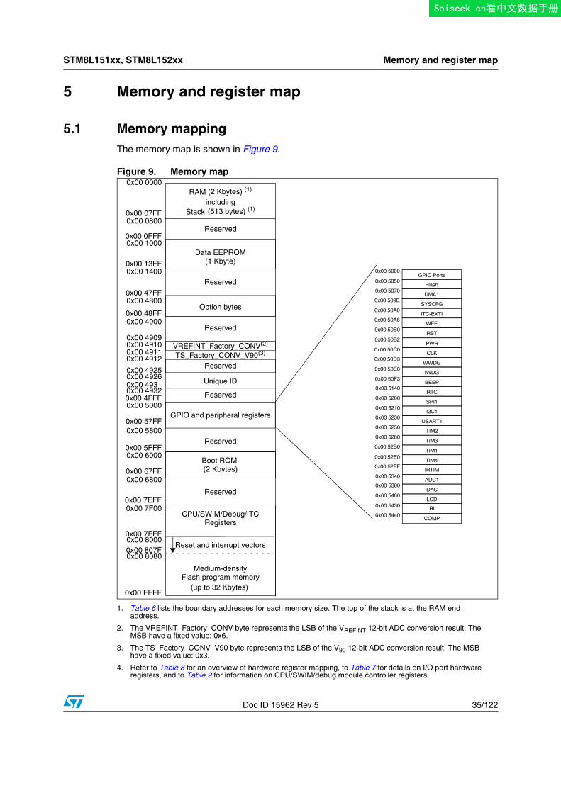
5 Memory and register map
5.1 Memory mappingThe memory map is shown in Figure 9.
Figure 9. Memory map
1. Table 6 lists the boundary addresses for each memory size. The top of the stack is at the RAM end address.
2. The VREFINT_Factory_CONV byte represents the LSB of the VREFINT 12-bit ADC conversion result. The MSB have a fixed value: 0x6.
3. The TS_Factory_CONV_V90 byte represents the LSB of the V90 12-bit ADC conversion result. The MSB have a fixed value: 0x3.
4. Refer to Table 8 for an overview of hardware register mapping, to Table 7 for details on I/O port hardware registers, and to Table 9 for information on CPU/SWIM/debug module controller registers.
GPIO and peripheral registers
0x00 0000
Reserved
Medium-density
(up to 32 Kbytes)
Reset and interrupt vectors
0x00 1000
0x00 13FF
RAM
0x00 07FF
(2 Kbytes) (1)
(513 bytes) (1)
0x00 1400
Data EEPROM
0x00 4800
0x00 48FF0x00 4900
0x00 7FFF0x00 8000
0x00 FFFF
0x00 0800
0x00 0FFF
0x00 47FF
0x00 7EFF
0x00 80800x00 807F
0x00 7F00
Reserved
Reserved
includingStack
(1 Kbyte)
Option bytes
0x00 4FFF0x00 5000
0x00 57FF0x00 5800
Reserved0x00 5FFF
Boot ROM 0x00 6000
0x00 67FF (2 Kbytes)0x00 6800
Reserved
CPU/SWIM/Debug/ITCRegisters
0x00 5000GPIO Ports
0x00 5050Flash
0x00 50C0
ITC-EXTI
0x00 50D3
RST
0x00 50E0
CLK
0x00 50F3
WWDG
0x00 5210
IWDG
0x00 5230
BEEP
0x00 5250
RTC
0x00 5280
SPI1
0x00 52B0
I2C1
0x00 52E0
USART1
TIM2
TIM3
TIM1
TIM4
IRTIM
ADC1
0x00 5070DMA1
SYSCFG
DAC
LCD
RI
0x00 509E
0x00 50A0
0x00 50B0
0x00 5140
0x00 5200
0x00 52FF
0x00 5340
0x00 5380
0x00 5400
0x00 5430
0x00 5440COMP
Flash program memory
WFE0x00 50A6
0x00 50B2PWR0x00 4910
0x00 4911
0x00 49260x00 4925
0x00 49310x00 4932
0x00 4909VREFINT_Factory_CONV(2)
TS_Factory_CONV_V90(3)0x00 4912
Reserved
Unique ID
Reserved
Soiseek.cn看中文数据手册
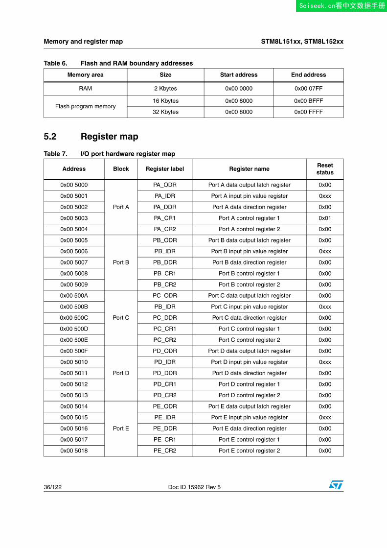
Memory and register map STM8L151xx, STM8L152xx
36/122 Doc ID 15962 Rev 5
5.2 Register map
Table 6. Flash and RAM boundary addresses
Memory area Size Start address End address
RAM 2 Kbytes 0x00 0000 0x00 07FF
Flash program memory16 Kbytes 0x00 8000 0x00 BFFF
32 Kbytes 0x00 8000 0x00 FFFF
Table 7. I/O port hardware register map
Address Block Register label Register nameReset status
0x00 5000
Port A
PA_ODR Port A data output latch register 0x00
0x00 5001 PA_IDR Port A input pin value register 0xxx
0x00 5002 PA_DDR Port A data direction register 0x00
0x00 5003 PA_CR1 Port A control register 1 0x01
0x00 5004 PA_CR2 Port A control register 2 0x00
0x00 5005
Port B
PB_ODR Port B data output latch register 0x00
0x00 5006 PB_IDR Port B input pin value register 0xxx
0x00 5007 PB_DDR Port B data direction register 0x00
0x00 5008 PB_CR1 Port B control register 1 0x00
0x00 5009 PB_CR2 Port B control register 2 0x00
0x00 500A
Port C
PC_ODR Port C data output latch register 0x00
0x00 500B PB_IDR Port C input pin value register 0xxx
0x00 500C PC_DDR Port C data direction register 0x00
0x00 500D PC_CR1 Port C control register 1 0x00
0x00 500E PC_CR2 Port C control register 2 0x00
0x00 500F
Port D
PD_ODR Port D data output latch register 0x00
0x00 5010 PD_IDR Port D input pin value register 0xxx
0x00 5011 PD_DDR Port D data direction register 0x00
0x00 5012 PD_CR1 Port D control register 1 0x00
0x00 5013 PD_CR2 Port D control register 2 0x00
0x00 5014
Port E
PE_ODR Port E data output latch register 0x00
0x00 5015 PE_IDR Port E input pin value register 0xxx
0x00 5016 PE_DDR Port E data direction register 0x00
0x00 5017 PE_CR1 Port E control register 1 0x00
0x00 5018 PE_CR2 Port E control register 2 0x00
Soiseek.cn看中文数据手册
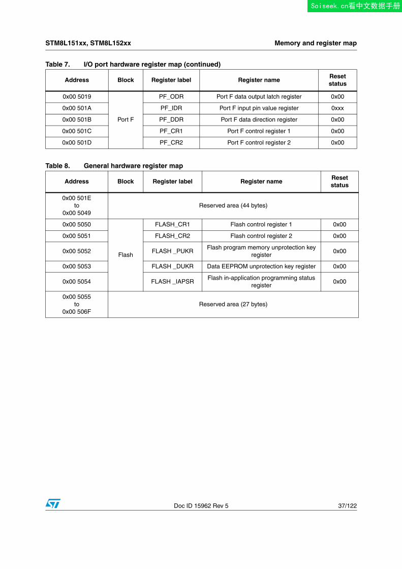
STM8L151xx, STM8L152xx Memory and register map
Doc ID 15962 Rev 5 37/122
0x00 5019
Port F
PF_ODR Port F data output latch register 0x00
0x00 501A PF_IDR Port F input pin value register 0xxx
0x00 501B PF_DDR Port F data direction register 0x00
0x00 501C PF_CR1 Port F control register 1 0x00
0x00 501D PF_CR2 Port F control register 2 0x00
Table 7. I/O port hardware register map (continued)
Address Block Register label Register nameReset status
Table 8. General hardware register map
Address Block Register label Register nameReset status
0x00 501Eto
0x00 5049Reserved area (44 bytes)
0x00 5050
Flash
FLASH_CR1 Flash control register 1 0x00
0x00 5051 FLASH_CR2 Flash control register 2 0x00
0x00 5052 FLASH _PUKRFlash program memory unprotection key
register0x00
0x00 5053 FLASH _DUKR Data EEPROM unprotection key register 0x00
0x00 5054 FLASH _IAPSRFlash in-application programming status
register0x00
0x00 5055to
0x00 506FReserved area (27 bytes)
Soiseek.cn看中文数据手册
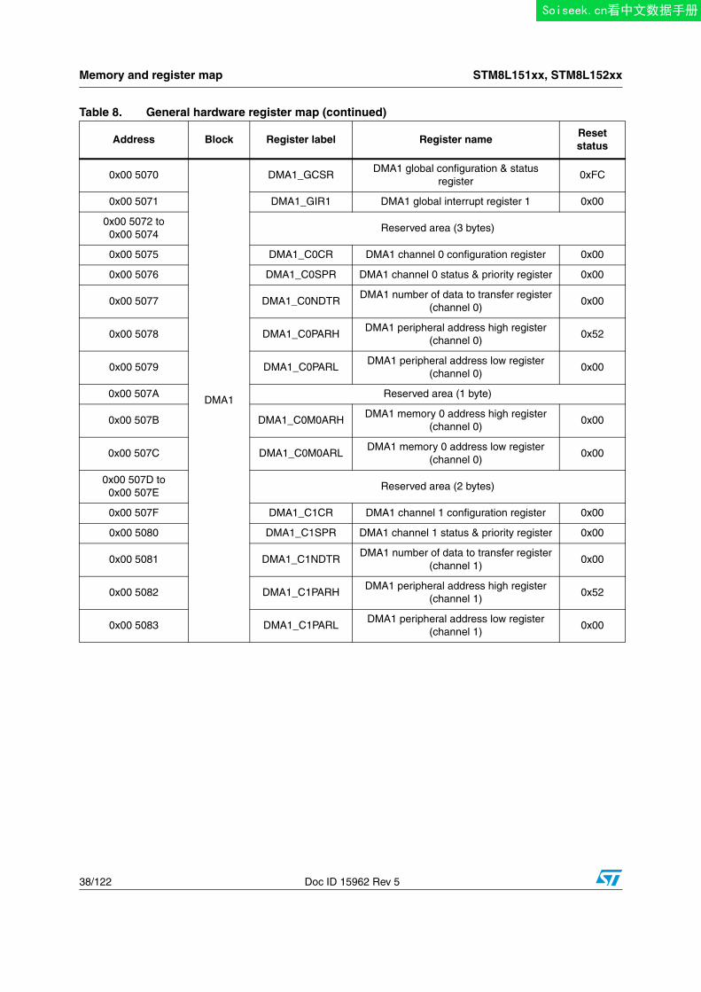
Memory and register map STM8L151xx, STM8L152xx
38/122 Doc ID 15962 Rev 5
0x00 5070
DMA1
DMA1_GCSRDMA1 global configuration & status
register0xFC
0x00 5071 DMA1_GIR1 DMA1 global interrupt register 1 0x00
0x00 5072 to0x00 5074
Reserved area (3 bytes)
0x00 5075 DMA1_C0CR DMA1 channel 0 configuration register 0x00
0x00 5076 DMA1_C0SPR DMA1 channel 0 status & priority register 0x00
0x00 5077 DMA1_C0NDTRDMA1 number of data to transfer register
(channel 0)0x00
0x00 5078 DMA1_C0PARHDMA1 peripheral address high register
(channel 0)0x52
0x00 5079 DMA1_C0PARLDMA1 peripheral address low register
(channel 0)0x00
0x00 507A Reserved area (1 byte)
0x00 507B DMA1_C0M0ARHDMA1 memory 0 address high register
(channel 0)0x00
0x00 507C DMA1_C0M0ARLDMA1 memory 0 address low register
(channel 0)0x00
0x00 507D to0x00 507E
Reserved area (2 bytes)
0x00 507F DMA1_C1CR DMA1 channel 1 configuration register 0x00
0x00 5080 DMA1_C1SPR DMA1 channel 1 status & priority register 0x00
0x00 5081 DMA1_C1NDTRDMA1 number of data to transfer register
(channel 1)0x00
0x00 5082 DMA1_C1PARHDMA1 peripheral address high register
(channel 1)0x52
0x00 5083 DMA1_C1PARLDMA1 peripheral address low register
(channel 1)0x00
Table 8. General hardware register map (continued)
Address Block Register label Register nameReset status
Soiseek.cn看中文数据手册
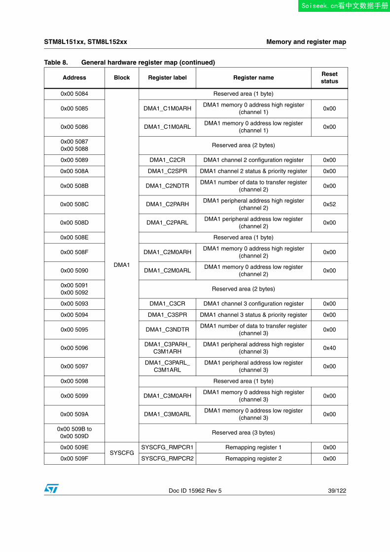
STM8L151xx, STM8L152xx Memory and register map
Doc ID 15962 Rev 5 39/122
0x00 5084
DMA1
Reserved area (1 byte)
0x00 5085 DMA1_C1M0ARHDMA1 memory 0 address high register
(channel 1)0x00
0x00 5086 DMA1_C1M0ARLDMA1 memory 0 address low register
(channel 1)0x00
0x00 50870x00 5088
Reserved area (2 bytes)
0x00 5089 DMA1_C2CR DMA1 channel 2 configuration register 0x00
0x00 508A DMA1_C2SPR DMA1 channel 2 status & priority register 0x00
0x00 508B DMA1_C2NDTRDMA1 number of data to transfer register
(channel 2)0x00
0x00 508C DMA1_C2PARHDMA1 peripheral address high register
(channel 2)0x52
0x00 508D DMA1_C2PARLDMA1 peripheral address low register
(channel 2)0x00
0x00 508E Reserved area (1 byte)
0x00 508F DMA1_C2M0ARHDMA1 memory 0 address high register
(channel 2)0x00
0x00 5090 DMA1_C2M0ARLDMA1 memory 0 address low register
(channel 2)0x00
0x00 50910x00 5092
Reserved area (2 bytes)
0x00 5093 DMA1_C3CR DMA1 channel 3 configuration register 0x00
0x00 5094 DMA1_C3SPR DMA1 channel 3 status & priority register 0x00
0x00 5095 DMA1_C3NDTRDMA1 number of data to transfer register
(channel 3)0x00
0x00 5096DMA1_C3PARH_
C3M1ARHDMA1 peripheral address high register
(channel 3)0x40
0x00 5097DMA1_C3PARL_
C3M1ARLDMA1 peripheral address low register
(channel 3)0x00
0x00 5098 Reserved area (1 byte)
0x00 5099 DMA1_C3M0ARHDMA1 memory 0 address high register
(channel 3)0x00
0x00 509A DMA1_C3M0ARLDMA1 memory 0 address low register
(channel 3)0x00
0x00 509B to 0x00 509D
Reserved area (3 bytes)
0x00 509ESYSCFG
SYSCFG_RMPCR1 Remapping register 1 0x00
0x00 509F SYSCFG_RMPCR2 Remapping register 2 0x00
Table 8. General hardware register map (continued)
Address Block Register label Register nameReset status
Soiseek.cn看中文数据手册
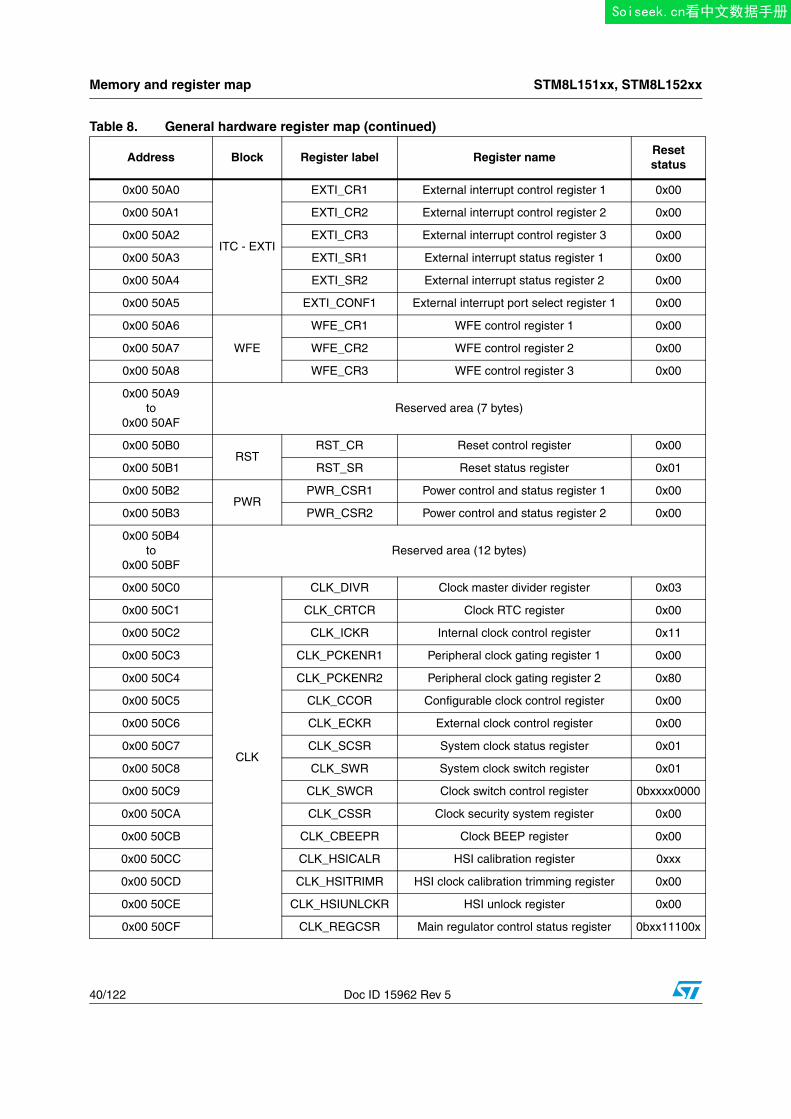
Memory and register map STM8L151xx, STM8L152xx
40/122 Doc ID 15962 Rev 5
0x00 50A0
ITC - EXTI
EXTI_CR1 External interrupt control register 1 0x00
0x00 50A1 EXTI_CR2 External interrupt control register 2 0x00
0x00 50A2 EXTI_CR3 External interrupt control register 3 0x00
0x00 50A3 EXTI_SR1 External interrupt status register 1 0x00
0x00 50A4 EXTI_SR2 External interrupt status register 2 0x00
0x00 50A5 EXTI_CONF1 External interrupt port select register 1 0x00
0x00 50A6
WFE
WFE_CR1 WFE control register 1 0x00
0x00 50A7 WFE_CR2 WFE control register 2 0x00
0x00 50A8 WFE_CR3 WFE control register 3 0x00
0x00 50A9to
0x00 50AFReserved area (7 bytes)
0x00 50B0RST
RST_CR Reset control register 0x00
0x00 50B1 RST_SR Reset status register 0x01
0x00 50B2PWR
PWR_CSR1 Power control and status register 1 0x00
0x00 50B3 PWR_CSR2 Power control and status register 2 0x00
0x00 50B4to
0x00 50BFReserved area (12 bytes)
0x00 50C0
CLK
CLK_DIVR Clock master divider register 0x03
0x00 50C1 CLK_CRTCR Clock RTC register 0x00
0x00 50C2 CLK_ICKR Internal clock control register 0x11
0x00 50C3 CLK_PCKENR1 Peripheral clock gating register 1 0x00
0x00 50C4 CLK_PCKENR2 Peripheral clock gating register 2 0x80
0x00 50C5 CLK_CCOR Configurable clock control register 0x00
0x00 50C6 CLK_ECKR External clock control register 0x00
0x00 50C7 CLK_SCSR System clock status register 0x01
0x00 50C8 CLK_SWR System clock switch register 0x01
0x00 50C9 CLK_SWCR Clock switch control register 0bxxxx0000
0x00 50CA CLK_CSSR Clock security system register 0x00
0x00 50CB CLK_CBEEPR Clock BEEP register 0x00
0x00 50CC CLK_HSICALR HSI calibration register 0xxx
0x00 50CD CLK_HSITRIMR HSI clock calibration trimming register 0x00
0x00 50CE CLK_HSIUNLCKR HSI unlock register 0x00
0x00 50CF CLK_REGCSR Main regulator control status register 0bxx11100x
Table 8. General hardware register map (continued)
Address Block Register label Register nameReset status
Soiseek.cn看中文数据手册
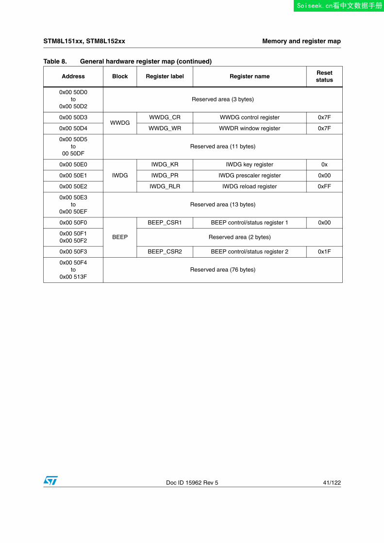
STM8L151xx, STM8L152xx Memory and register map
Doc ID 15962 Rev 5 41/122
0x00 50D0to
0x00 50D2Reserved area (3 bytes)
0x00 50D3WWDG
WWDG_CR WWDG control register 0x7F
0x00 50D4 WWDG_WR WWDR window register 0x7F
0x00 50D5to
00 50DFReserved area (11 bytes)
0x00 50E0
IWDG
IWDG_KR IWDG key register 0x
0x00 50E1 IWDG_PR IWDG prescaler register 0x00
0x00 50E2 IWDG_RLR IWDG reload register 0xFF
0x00 50E3to
0x00 50EFReserved area (13 bytes)
0x00 50F0
BEEP
BEEP_CSR1 BEEP control/status register 1 0x00
0x00 50F10x00 50F2
Reserved area (2 bytes)
0x00 50F3 BEEP_CSR2 BEEP control/status register 2 0x1F
0x00 50F4to
0x00 513FReserved area (76 bytes)
Table 8. General hardware register map (continued)
Address Block Register label Register nameReset status
Soiseek.cn看中文数据手册
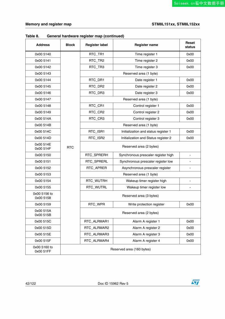
Memory and register map STM8L151xx, STM8L152xx
42/122 Doc ID 15962 Rev 5
0x00 5140
RTC
RTC_TR1 Time register 1 0x00
0x00 5141 RTC_TR2 Time register 2 0x00
0x00 5142 RTC_TR3 Time register 3 0x00
0x00 5143 Reserved area (1 byte)
0x00 5144 RTC_DR1 Date register 1 0x00
0x00 5145 RTC_DR2 Date register 2 0x00
0x00 5146 RTC_DR3 Date register 3 0x00
0x00 5147 Reserved area (1 byte)
0x00 5148 RTC_CR1 Control register 1 0x00
0x00 5149 RTC_CR2 Control register 2 0x00
0x00 514A RTC_CR3 Control register 3 0x00
0x00 514B Reserved area (1 byte)
0x00 514C RTC_ISR1 Initialization and status register 1 0x00
0x00 514D RTC_ISR2 Initialization and Status register 2 0x00
0x00 514E0x00 514F
Reserved area (2 bytes)
0x00 5150 RTC_SPRERH Synchronous prescaler register high -
0x00 5151 RTC_SPRERL Synchronous prescaler register low -
0x00 5152 RTC_APRER Asynchronous prescaler register -
0x00 5153 Reserved area (1 byte)
0x00 5154 RTC_WUTRH Wakeup timer register high -
0x00 5155 RTC_WUTRL Wakeup timer register low -
0x00 5156 to 0x00 5158
Reserved area (3 bytes)
0x00 5159 RTC_WPR Write protection register 0x00
0x00 515A0x00 515B
Reserved area (2 bytes)
0x00 515C RTC_ALRMAR1 Alarm A register 1 0x00
0x00 515D RTC_ALRMAR2 Alarm A register 2 0x00
0x00 515E RTC_ALRMAR3 Alarm A register 3 0x00
0x00 515F RTC_ALRMAR4 Alarm A register 4 0x00
0x00 5160 to0x00 51FF
Reserved area (160 bytes)
Table 8. General hardware register map (continued)
Address Block Register label Register nameReset status
Soiseek.cn看中文数据手册
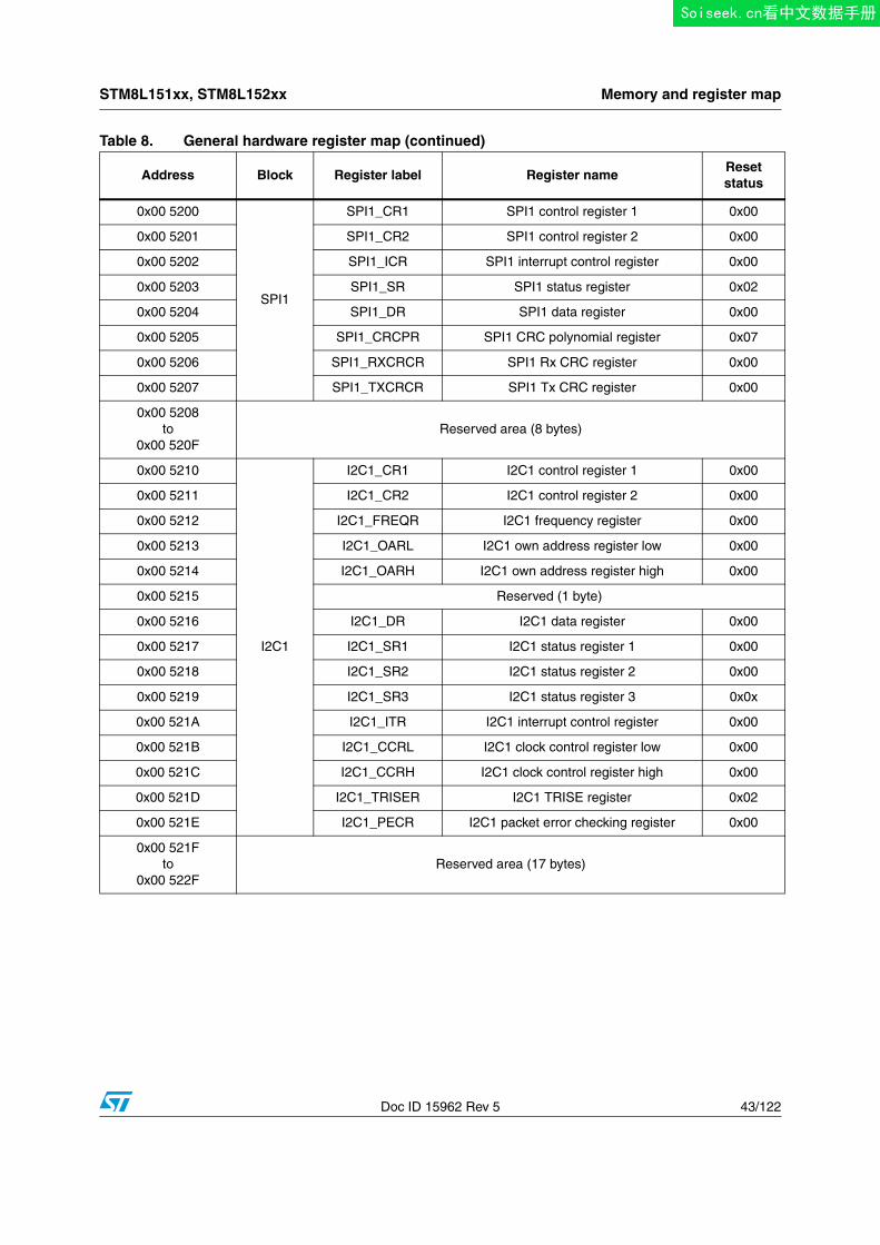
STM8L151xx, STM8L152xx Memory and register map
Doc ID 15962 Rev 5 43/122
0x00 5200
SPI1
SPI1_CR1 SPI1 control register 1 0x00
0x00 5201 SPI1_CR2 SPI1 control register 2 0x00
0x00 5202 SPI1_ICR SPI1 interrupt control register 0x00
0x00 5203 SPI1_SR SPI1 status register 0x02
0x00 5204 SPI1_DR SPI1 data register 0x00
0x00 5205 SPI1_CRCPR SPI1 CRC polynomial register 0x07
0x00 5206 SPI1_RXCRCR SPI1 Rx CRC register 0x00
0x00 5207 SPI1_TXCRCR SPI1 Tx CRC register 0x00
0x00 5208to
0x00 520FReserved area (8 bytes)
0x00 5210
I2C1
I2C1_CR1 I2C1 control register 1 0x00
0x00 5211 I2C1_CR2 I2C1 control register 2 0x00
0x00 5212 I2C1_FREQR I2C1 frequency register 0x00
0x00 5213 I2C1_OARL I2C1 own address register low 0x00
0x00 5214 I2C1_OARH I2C1 own address register high 0x00
0x00 5215 Reserved (1 byte)
0x00 5216 I2C1_DR I2C1 data register 0x00
0x00 5217 I2C1_SR1 I2C1 status register 1 0x00
0x00 5218 I2C1_SR2 I2C1 status register 2 0x00
0x00 5219 I2C1_SR3 I2C1 status register 3 0x0x
0x00 521A I2C1_ITR I2C1 interrupt control register 0x00
0x00 521B I2C1_CCRL I2C1 clock control register low 0x00
0x00 521C I2C1_CCRH I2C1 clock control register high 0x00
0x00 521D I2C1_TRISER I2C1 TRISE register 0x02
0x00 521E I2C1_PECR I2C1 packet error checking register 0x00
0x00 521Fto
0x00 522FReserved area (17 bytes)
Table 8. General hardware register map (continued)
Address Block Register label Register nameReset status
Soiseek.cn看中文数据手册
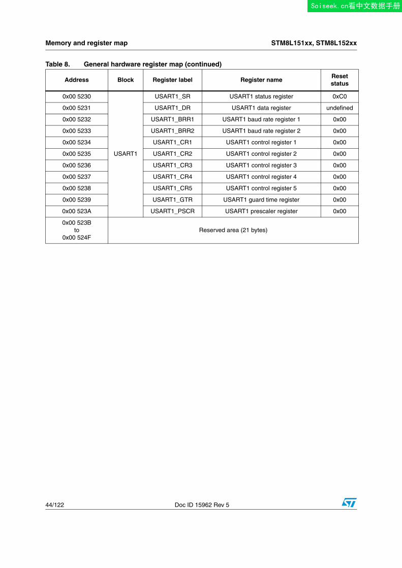
Memory and register map STM8L151xx, STM8L152xx
44/122 Doc ID 15962 Rev 5
0x00 5230
USART1
USART1_SR USART1 status register 0xC0
0x00 5231 USART1_DR USART1 data register undefined
0x00 5232 USART1_BRR1 USART1 baud rate register 1 0x00
0x00 5233 USART1_BRR2 USART1 baud rate register 2 0x00
0x00 5234 USART1_CR1 USART1 control register 1 0x00
0x00 5235 USART1_CR2 USART1 control register 2 0x00
0x00 5236 USART1_CR3 USART1 control register 3 0x00
0x00 5237 USART1_CR4 USART1 control register 4 0x00
0x00 5238 USART1_CR5 USART1 control register 5 0x00
0x00 5239 USART1_GTR USART1 guard time register 0x00
0x00 523A USART1_PSCR USART1 prescaler register 0x00
0x00 523Bto
0x00 524FReserved area (21 bytes)
Table 8. General hardware register map (continued)
Address Block Register label Register nameReset status
Soiseek.cn看中文数据手册
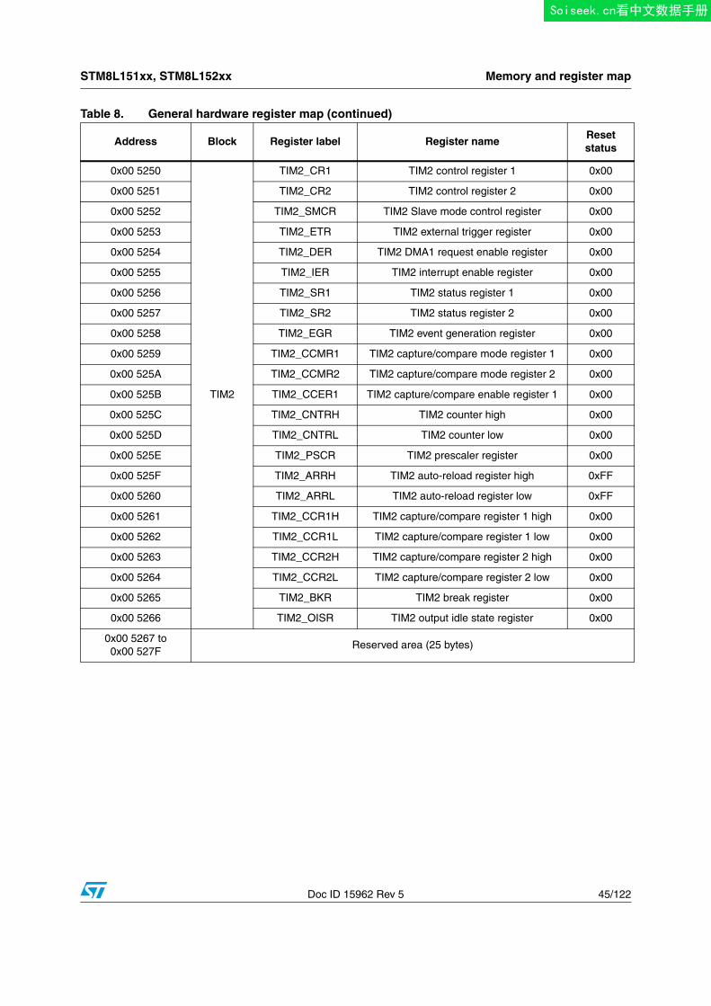
STM8L151xx, STM8L152xx Memory and register map
Doc ID 15962 Rev 5 45/122
0x00 5250
TIM2
TIM2_CR1 TIM2 control register 1 0x00
0x00 5251 TIM2_CR2 TIM2 control register 2 0x00
0x00 5252 TIM2_SMCR TIM2 Slave mode control register 0x00
0x00 5253 TIM2_ETR TIM2 external trigger register 0x00
0x00 5254 TIM2_DER TIM2 DMA1 request enable register 0x00
0x00 5255 TIM2_IER TIM2 interrupt enable register 0x00
0x00 5256 TIM2_SR1 TIM2 status register 1 0x00
0x00 5257 TIM2_SR2 TIM2 status register 2 0x00
0x00 5258 TIM2_EGR TIM2 event generation register 0x00
0x00 5259 TIM2_CCMR1 TIM2 capture/compare mode register 1 0x00
0x00 525A TIM2_CCMR2 TIM2 capture/compare mode register 2 0x00
0x00 525B TIM2_CCER1 TIM2 capture/compare enable register 1 0x00
0x00 525C TIM2_CNTRH TIM2 counter high 0x00
0x00 525D TIM2_CNTRL TIM2 counter low 0x00
0x00 525E TIM2_PSCR TIM2 prescaler register 0x00
0x00 525F TIM2_ARRH TIM2 auto-reload register high 0xFF
0x00 5260 TIM2_ARRL TIM2 auto-reload register low 0xFF
0x00 5261 TIM2_CCR1H TIM2 capture/compare register 1 high 0x00
0x00 5262 TIM2_CCR1L TIM2 capture/compare register 1 low 0x00
0x00 5263 TIM2_CCR2H TIM2 capture/compare register 2 high 0x00
0x00 5264 TIM2_CCR2L TIM2 capture/compare register 2 low 0x00
0x00 5265 TIM2_BKR TIM2 break register 0x00
0x00 5266 TIM2_OISR TIM2 output idle state register 0x00
0x00 5267 to0x00 527F
Reserved area (25 bytes)
Table 8. General hardware register map (continued)
Address Block Register label Register nameReset status
Soiseek.cn看中文数据手册
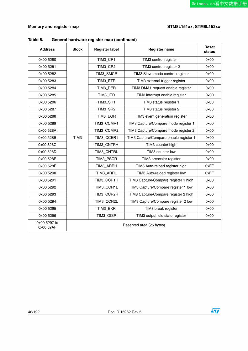
Memory and register map STM8L151xx, STM8L152xx
46/122 Doc ID 15962 Rev 5
0x00 5280
TIM3
TIM3_CR1 TIM3 control register 1 0x00
0x00 5281 TIM3_CR2 TIM3 control register 2 0x00
0x00 5282 TIM3_SMCR TIM3 Slave mode control register 0x00
0x00 5283 TIM3_ETR TIM3 external trigger register 0x00
0x00 5284 TIM3_DER TIM3 DMA1 request enable register 0x00
0x00 5285 TIM3_IER TIM3 interrupt enable register 0x00
0x00 5286 TIM3_SR1 TIM3 status register 1 0x00
0x00 5287 TIM3_SR2 TIM3 status register 2 0x00
0x00 5288 TIM3_EGR TIM3 event generation register 0x00
0x00 5289 TIM3_CCMR1 TIM3 Capture/Compare mode register 1 0x00
0x00 528A TIM3_CCMR2 TIM3 Capture/Compare mode register 2 0x00
0x00 528B TIM3_CCER1 TIM3 Capture/Compare enable register 1 0x00
0x00 528C TIM3_CNTRH TIM3 counter high 0x00
0x00 528D TIM3_CNTRL TIM3 counter low 0x00
0x00 528E TIM3_PSCR TIM3 prescaler register 0x00
0x00 528F TIM3_ARRH TIM3 Auto-reload register high 0xFF
0x00 5290 TIM3_ARRL TIM3 Auto-reload register low 0xFF
0x00 5291 TIM3_CCR1H TIM3 Capture/Compare register 1 high 0x00
0x00 5292 TIM3_CCR1L TIM3 Capture/Compare register 1 low 0x00
0x00 5293 TIM3_CCR2H TIM3 Capture/Compare register 2 high 0x00
0x00 5294 TIM3_CCR2L TIM3 Capture/Compare register 2 low 0x00
0x00 5295 TIM3_BKR TIM3 break register 0x00
0x00 5296 TIM3_OISR TIM3 output idle state register 0x00
0x00 5297 to0x00 52AF
Reserved area (25 bytes)
Table 8. General hardware register map (continued)
Address Block Register label Register nameReset status
Soiseek.cn看中文数据手册
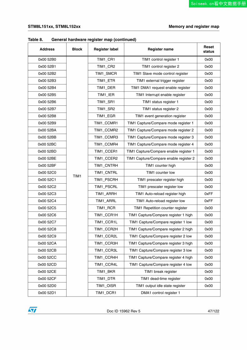
STM8L151xx, STM8L152xx Memory and register map
Doc ID 15962 Rev 5 47/122
0x00 52B0
TIM1
TIM1_CR1 TIM1 control register 1 0x00
0x00 52B1 TIM1_CR2 TIM1 control register 2 0x00
0x00 52B2 TIM1_SMCR TIM1 Slave mode control register 0x00
0x00 52B3 TIM1_ETR TIM1 external trigger register 0x00
0x00 52B4 TIM1_DER TIM1 DMA1 request enable register 0x00
0x00 52B5 TIM1_IER TIM1 Interrupt enable register 0x00
0x00 52B6 TIM1_SR1 TIM1 status register 1 0x00
0x00 52B7 TIM1_SR2 TIM1 status register 2 0x00
0x00 52B8 TIM1_EGR TIM1 event generation register 0x00
0x00 52B9 TIM1_CCMR1 TIM1 Capture/Compare mode register 1 0x00
0x00 52BA TIM1_CCMR2 TIM1 Capture/Compare mode register 2 0x00
0x00 52BB TIM1_CCMR3 TIM1 Capture/Compare mode register 3 0x00
0x00 52BC TIM1_CCMR4 TIM1 Capture/Compare mode register 4 0x00
0x00 52BD TIM1_CCER1 TIM1 Capture/Compare enable register 1 0x00
0x00 52BE TIM1_CCER2 TIM1 Capture/Compare enable register 2 0x00
0x00 52BF TIM1_CNTRH TIM1 counter high 0x00
0x00 52C0 TIM1_CNTRL TIM1 counter low 0x00
0x00 52C1 TIM1_PSCRH TIM1 prescaler register high 0x00
0x00 52C2 TIM1_PSCRL TIM1 prescaler register low 0x00
0x00 52C3 TIM1_ARRH TIM1 Auto-reload register high 0xFF
0x00 52C4 TIM1_ARRL TIM1 Auto-reload register low 0xFF
0x00 52C5 TIM1_RCR TIM1 Repetition counter register 0x00
0x00 52C6 TIM1_CCR1H TIM1 Capture/Compare register 1 high 0x00
0x00 52C7 TIM1_CCR1L TIM1 Capture/Compare register 1 low 0x00
0x00 52C8 TIM1_CCR2H TIM1 Capture/Compare register 2 high 0x00
0x00 52C9 TIM1_CCR2L TIM1 Capture/Compare register 2 low 0x00
0x00 52CA TIM1_CCR3H TIM1 Capture/Compare register 3 high 0x00
0x00 52CB TIM1_CCR3L TIM1 Capture/Compare register 3 low 0x00
0x00 52CC TIM1_CCR4H TIM1 Capture/Compare register 4 high 0x00
0x00 52CD TIM1_CCR4L TIM1 Capture/Compare register 4 low 0x00
0x00 52CE TIM1_BKR TIM1 break register 0x00
0x00 52CF TIM1_DTR TIM1 dead-time register 0x00
0x00 52D0 TIM1_OISR TIM1 output idle state register 0x00
0x00 52D1 TIM1_DCR1 DMA1 control register 1
Table 8. General hardware register map (continued)
Address Block Register label Register nameReset status
Soiseek.cn看中文数据手册
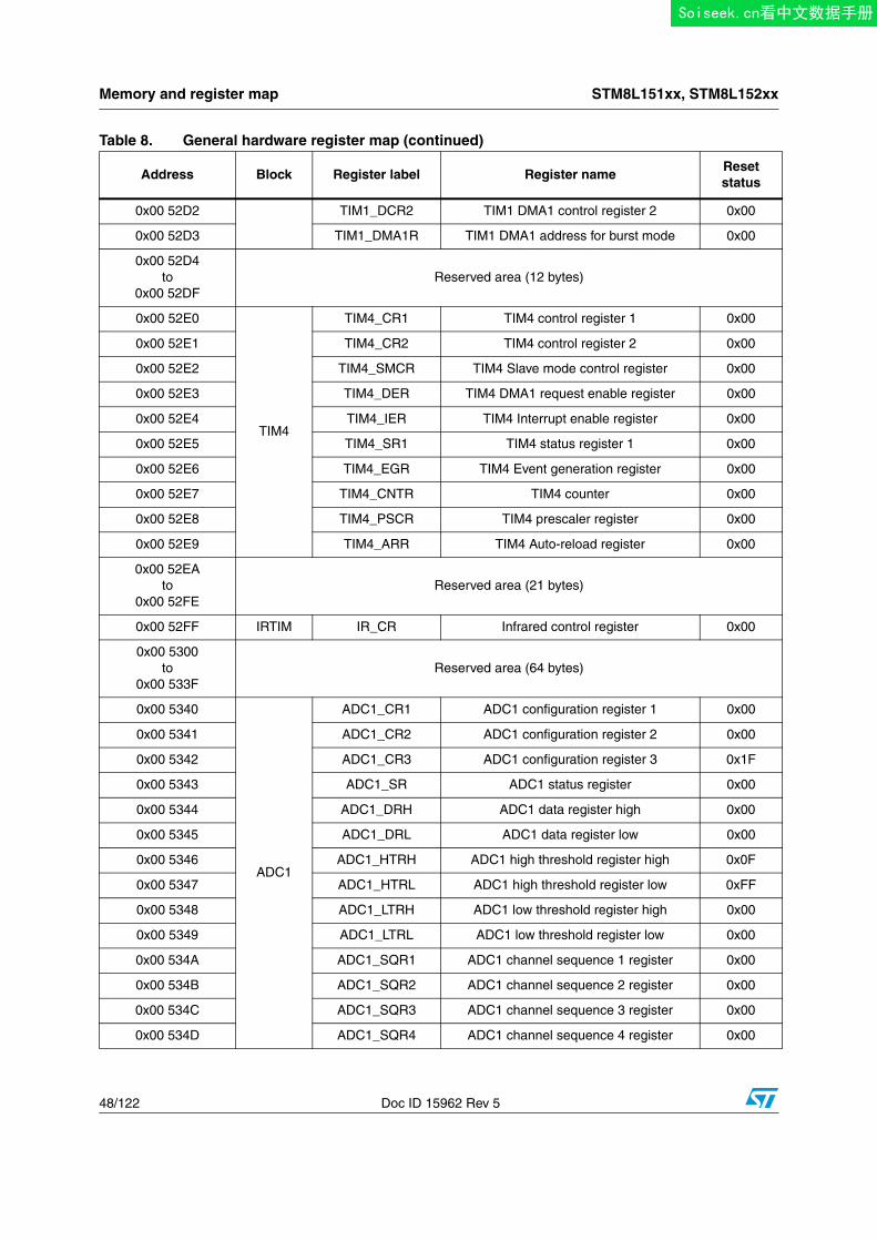
Memory and register map STM8L151xx, STM8L152xx
48/122 Doc ID 15962 Rev 5
0x00 52D2 TIM1_DCR2 TIM1 DMA1 control register 2 0x00
0x00 52D3 TIM1_DMA1R TIM1 DMA1 address for burst mode 0x00
0x00 52D4to
0x00 52DFReserved area (12 bytes)
0x00 52E0
TIM4
TIM4_CR1 TIM4 control register 1 0x00
0x00 52E1 TIM4_CR2 TIM4 control register 2 0x00
0x00 52E2 TIM4_SMCR TIM4 Slave mode control register 0x00
0x00 52E3 TIM4_DER TIM4 DMA1 request enable register 0x00
0x00 52E4 TIM4_IER TIM4 Interrupt enable register 0x00
0x00 52E5 TIM4_SR1 TIM4 status register 1 0x00
0x00 52E6 TIM4_EGR TIM4 Event generation register 0x00
0x00 52E7 TIM4_CNTR TIM4 counter 0x00
0x00 52E8 TIM4_PSCR TIM4 prescaler register 0x00
0x00 52E9 TIM4_ARR TIM4 Auto-reload register 0x00
0x00 52EAto
0x00 52FEReserved area (21 bytes)
0x00 52FF IRTIM IR_CR Infrared control register 0x00
0x00 5300to
0x00 533FReserved area (64 bytes)
0x00 5340
ADC1
ADC1_CR1 ADC1 configuration register 1 0x00
0x00 5341 ADC1_CR2 ADC1 configuration register 2 0x00
0x00 5342 ADC1_CR3 ADC1 configuration register 3 0x1F
0x00 5343 ADC1_SR ADC1 status register 0x00
0x00 5344 ADC1_DRH ADC1 data register high 0x00
0x00 5345 ADC1_DRL ADC1 data register low 0x00
0x00 5346 ADC1_HTRH ADC1 high threshold register high 0x0F
0x00 5347 ADC1_HTRL ADC1 high threshold register low 0xFF
0x00 5348 ADC1_LTRH ADC1 low threshold register high 0x00
0x00 5349 ADC1_LTRL ADC1 low threshold register low 0x00
0x00 534A ADC1_SQR1 ADC1 channel sequence 1 register 0x00
0x00 534B ADC1_SQR2 ADC1 channel sequence 2 register 0x00
0x00 534C ADC1_SQR3 ADC1 channel sequence 3 register 0x00
0x00 534D ADC1_SQR4 ADC1 channel sequence 4 register 0x00
Table 8. General hardware register map (continued)
Address Block Register label Register nameReset status
Soiseek.cn看中文数据手册
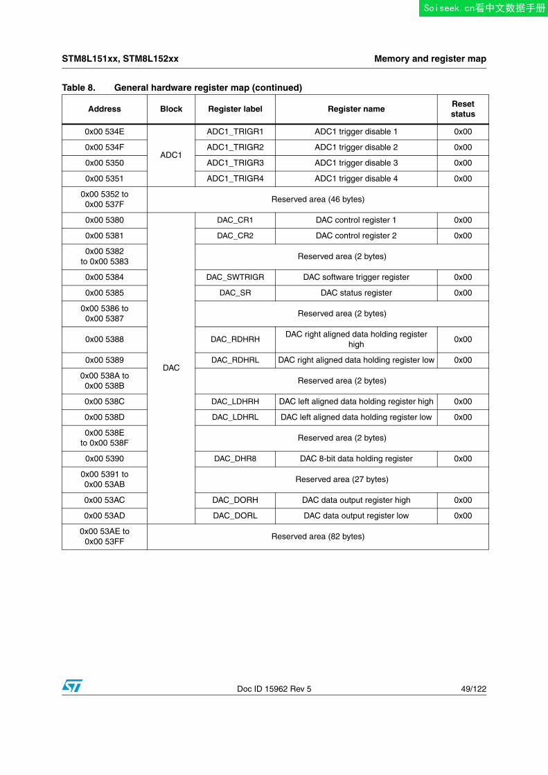
STM8L151xx, STM8L152xx Memory and register map
Doc ID 15962 Rev 5 49/122
0x00 534E
ADC1
ADC1_TRIGR1 ADC1 trigger disable 1 0x00
0x00 534F ADC1_TRIGR2 ADC1 trigger disable 2 0x00
0x00 5350 ADC1_TRIGR3 ADC1 trigger disable 3 0x00
0x00 5351 ADC1_TRIGR4 ADC1 trigger disable 4 0x00
0x00 5352 to 0x00 537F
Reserved area (46 bytes)
0x00 5380
DAC
DAC_CR1 DAC control register 1 0x00
0x00 5381 DAC_CR2 DAC control register 2 0x00
0x00 5382 to 0x00 5383
Reserved area (2 bytes)
0x00 5384 DAC_SWTRIGR DAC software trigger register 0x00
0x00 5385 DAC_SR DAC status register 0x00
0x00 5386 to 0x00 5387
Reserved area (2 bytes)
0x00 5388 DAC_RDHRHDAC right aligned data holding register
high0x00
0x00 5389 DAC_RDHRL DAC right aligned data holding register low 0x00
0x00 538A to0x00 538B
Reserved area (2 bytes)
0x00 538C DAC_LDHRH DAC left aligned data holding register high 0x00
0x00 538D DAC_LDHRL DAC left aligned data holding register low 0x00
0x00 538Eto 0x00 538F
Reserved area (2 bytes)
0x00 5390 DAC_DHR8 DAC 8-bit data holding register 0x00
0x00 5391 to0x00 53AB
Reserved area (27 bytes)
0x00 53AC DAC_DORH DAC data output register high 0x00
0x00 53AD DAC_DORL DAC data output register low 0x00
0x00 53AE to 0x00 53FF
Reserved area (82 bytes)
Table 8. General hardware register map (continued)
Address Block Register label Register nameReset status
Soiseek.cn看中文数据手册
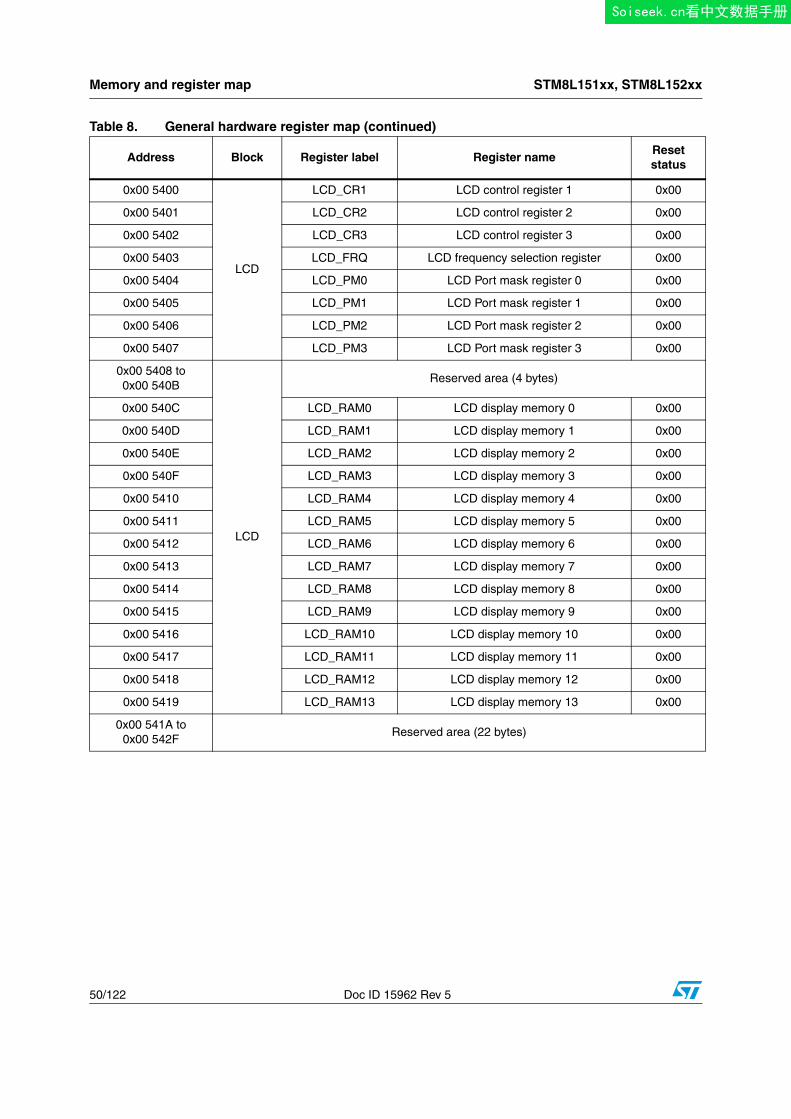
Memory and register map STM8L151xx, STM8L152xx
50/122 Doc ID 15962 Rev 5
0x00 5400
LCD
LCD_CR1 LCD control register 1 0x00
0x00 5401 LCD_CR2 LCD control register 2 0x00
0x00 5402 LCD_CR3 LCD control register 3 0x00
0x00 5403 LCD_FRQ LCD frequency selection register 0x00
0x00 5404 LCD_PM0 LCD Port mask register 0 0x00
0x00 5405 LCD_PM1 LCD Port mask register 1 0x00
0x00 5406 LCD_PM2 LCD Port mask register 2 0x00
0x00 5407 LCD_PM3 LCD Port mask register 3 0x00
0x00 5408 to 0x00 540B
LCD
Reserved area (4 bytes)
0x00 540C LCD_RAM0 LCD display memory 0 0x00
0x00 540D LCD_RAM1 LCD display memory 1 0x00
0x00 540E LCD_RAM2 LCD display memory 2 0x00
0x00 540F LCD_RAM3 LCD display memory 3 0x00
0x00 5410 LCD_RAM4 LCD display memory 4 0x00
0x00 5411 LCD_RAM5 LCD display memory 5 0x00
0x00 5412 LCD_RAM6 LCD display memory 6 0x00
0x00 5413 LCD_RAM7 LCD display memory 7 0x00
0x00 5414 LCD_RAM8 LCD display memory 8 0x00
0x00 5415 LCD_RAM9 LCD display memory 9 0x00
0x00 5416 LCD_RAM10 LCD display memory 10 0x00
0x00 5417 LCD_RAM11 LCD display memory 11 0x00
0x00 5418 LCD_RAM12 LCD display memory 12 0x00
0x00 5419 LCD_RAM13 LCD display memory 13 0x00
0x00 541A to 0x00 542F
Reserved area (22 bytes)
Table 8. General hardware register map (continued)
Address Block Register label Register nameReset status
Soiseek.cn看中文数据手册
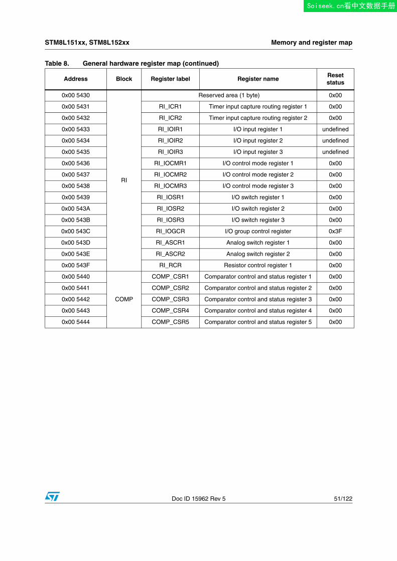
STM8L151xx, STM8L152xx Memory and register map
Doc ID 15962 Rev 5 51/122
0x00 5430
RI
Reserved area (1 byte) 0x00
0x00 5431 RI_ICR1 Timer input capture routing register 1 0x00
0x00 5432 RI_ICR2 Timer input capture routing register 2 0x00
0x00 5433 RI_IOIR1 I/O input register 1 undefined
0x00 5434 RI_IOIR2 I/O input register 2 undefined
0x00 5435 RI_IOIR3 I/O input register 3 undefined
0x00 5436 RI_IOCMR1 I/O control mode register 1 0x00
0x00 5437 RI_IOCMR2 I/O control mode register 2 0x00
0x00 5438 RI_IOCMR3 I/O control mode register 3 0x00
0x00 5439 RI_IOSR1 I/O switch register 1 0x00
0x00 543A RI_IOSR2 I/O switch register 2 0x00
0x00 543B RI_IOSR3 I/O switch register 3 0x00
0x00 543C RI_IOGCR I/O group control register 0x3F
0x00 543D RI_ASCR1 Analog switch register 1 0x00
0x00 543E RI_ASCR2 Analog switch register 2 0x00
0x00 543F RI_RCR Resistor control register 1 0x00
0x00 5440
COMP
COMP_CSR1 Comparator control and status register 1 0x00
0x00 5441 COMP_CSR2 Comparator control and status register 2 0x00
0x00 5442 COMP_CSR3 Comparator control and status register 3 0x00
0x00 5443 COMP_CSR4 Comparator control and status register 4 0x00
0x00 5444 COMP_CSR5 Comparator control and status register 5 0x00
Table 8. General hardware register map (continued)
Address Block Register label Register nameReset status
Soiseek.cn看中文数据手册
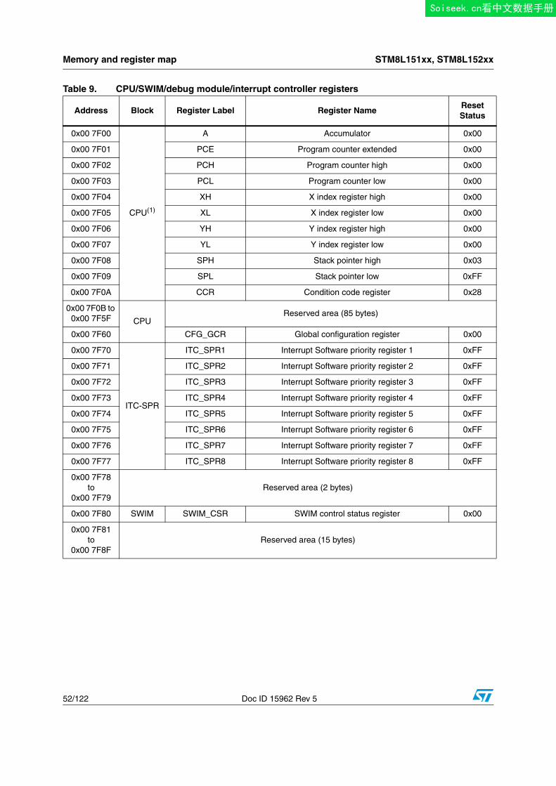
Memory and register map STM8L151xx, STM8L152xx
52/122 Doc ID 15962 Rev 5
Table 9. CPU/SWIM/debug module/interrupt controller registers
Address Block Register Label Register NameReset Status
0x00 7F00
CPU(1)
A Accumulator 0x00
0x00 7F01 PCE Program counter extended 0x00
0x00 7F02 PCH Program counter high 0x00
0x00 7F03 PCL Program counter low 0x00
0x00 7F04 XH X index register high 0x00
0x00 7F05 XL X index register low 0x00
0x00 7F06 YH Y index register high 0x00
0x00 7F07 YL Y index register low 0x00
0x00 7F08 SPH Stack pointer high 0x03
0x00 7F09 SPL Stack pointer low 0xFF
0x00 7F0A CCR Condition code register 0x28
0x00 7F0B to 0x00 7F5F CPU
Reserved area (85 bytes)
0x00 7F60 CFG_GCR Global configuration register 0x00
0x00 7F70
ITC-SPR
ITC_SPR1 Interrupt Software priority register 1 0xFF
0x00 7F71 ITC_SPR2 Interrupt Software priority register 2 0xFF
0x00 7F72 ITC_SPR3 Interrupt Software priority register 3 0xFF
0x00 7F73 ITC_SPR4 Interrupt Software priority register 4 0xFF
0x00 7F74 ITC_SPR5 Interrupt Software priority register 5 0xFF
0x00 7F75 ITC_SPR6 Interrupt Software priority register 6 0xFF
0x00 7F76 ITC_SPR7 Interrupt Software priority register 7 0xFF
0x00 7F77 ITC_SPR8 Interrupt Software priority register 8 0xFF
0x00 7F78to
0x00 7F79Reserved area (2 bytes)
0x00 7F80 SWIM SWIM_CSR SWIM control status register 0x00
0x00 7F81to
0x00 7F8FReserved area (15 bytes)
Soiseek.cn看中文数据手册
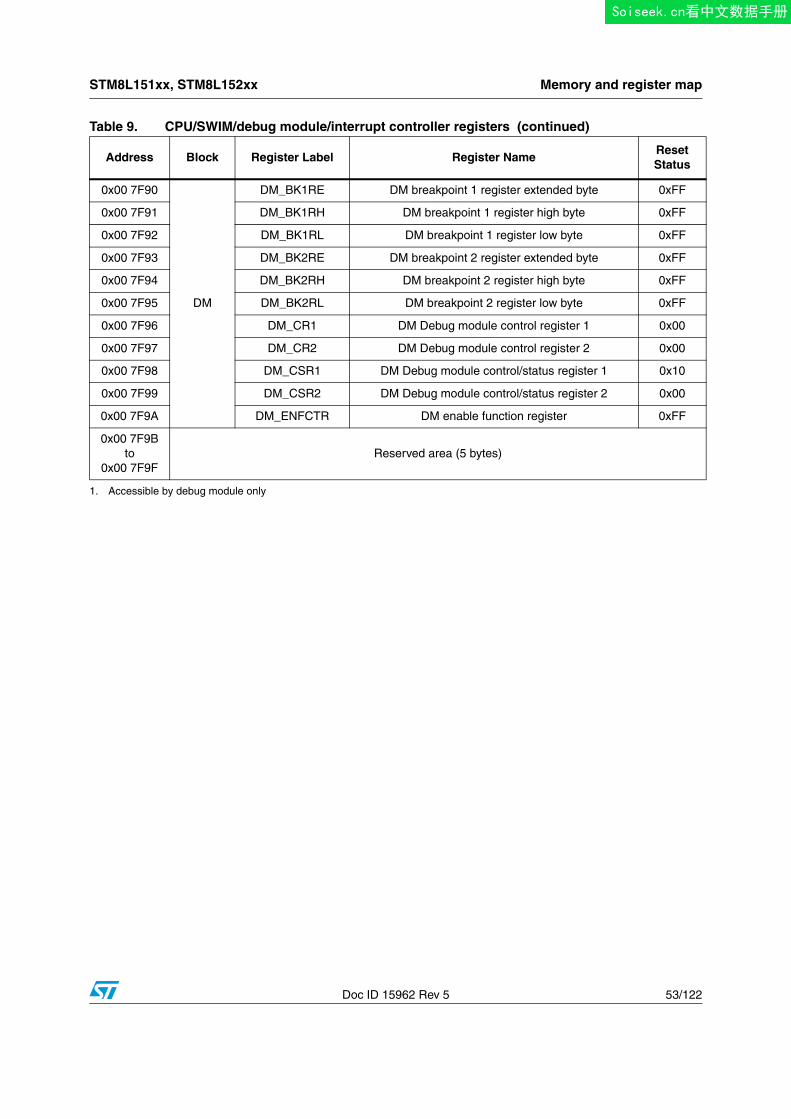
STM8L151xx, STM8L152xx Memory and register map
Doc ID 15962 Rev 5 53/122
0x00 7F90
DM
DM_BK1RE DM breakpoint 1 register extended byte 0xFF
0x00 7F91 DM_BK1RH DM breakpoint 1 register high byte 0xFF
0x00 7F92 DM_BK1RL DM breakpoint 1 register low byte 0xFF
0x00 7F93 DM_BK2RE DM breakpoint 2 register extended byte 0xFF
0x00 7F94 DM_BK2RH DM breakpoint 2 register high byte 0xFF
0x00 7F95 DM_BK2RL DM breakpoint 2 register low byte 0xFF
0x00 7F96 DM_CR1 DM Debug module control register 1 0x00
0x00 7F97 DM_CR2 DM Debug module control register 2 0x00
0x00 7F98 DM_CSR1 DM Debug module control/status register 1 0x10
0x00 7F99 DM_CSR2 DM Debug module control/status register 2 0x00
0x00 7F9A DM_ENFCTR DM enable function register 0xFF
0x00 7F9Bto
0x00 7F9FReserved area (5 bytes)
1. Accessible by debug module only
Table 9. CPU/SWIM/debug module/interrupt controller registers (continued)
Address Block Register Label Register NameReset Status
Soiseek.cn看中文数据手册
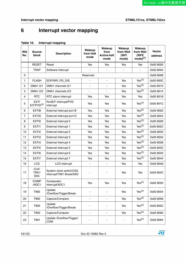
Interrupt vector mapping STM8L151xx, STM8L152xx
54/122 Doc ID 15962 Rev 5
6 Interrupt vector mapping
Table 10. Interrupt mapping
IRQNo.
Source block
DescriptionWakeup
from Halt mode
Wakeup from
Active-halt mode
Wakeup from Wait
(WFI mode)
Wakeup from Wait
(WFE mode)(1)
Vector
address
RESET Reset Yes Yes Yes Yes 0x00 8000
TRAP Software interrupt - - - - 0x00 8004
0 Reserved 0x00 8008
1 FLASH EOP/WR_PG_DIS - - Yes Yes(2) 0x00 800C
2 DMA1 0/1 DMA1 channels 0/1 - - Yes Yes(2) 0x00 8010
3 DMA1 2/3 DMA1 channels 2/3 - - Yes Yes(2) 0x00 8014
4 RTC RTC alarm interrupt Yes Yes Yes Yes 0x00 8018
5EXTI
E/F/PVD(3)PortE/F interrupt/PVD interrupt
Yes Yes Yes Yes(2) 0x00 801C
6 EXTIB External interrupt port B Yes Yes Yes Yes(2) 0x00 8020
7 EXTID External interrupt port D Yes Yes Yes Yes(2) 0x00 8024
8 EXTI0 External interrupt 0 Yes Yes Yes Yes(2) 0x00 8028
9 EXTI1 External interrupt 1 Yes Yes Yes Yes(2) 0x00 802C
10 EXTI2 External interrupt 2 Yes Yes Yes Yes(2) 0x00 8030
11 EXTI3 External interrupt 3 Yes Yes Yes Yes(2) 0x00 8034
12 EXTI4 External interrupt 4 Yes Yes Yes Yes(2) 0x00 8038
13 EXTI5 External interrupt 5 Yes Yes Yes Yes(2) 0x00 803C
14 EXTI6 External interrupt 6 Yes Yes Yes Yes(2) 0x00 8040
15 EXTI7 External interrupt 7 Yes Yes Yes Yes(2) 0x00 8044
16 LCD LCD interrupt - - Yes Yes 0x00 8048
17CLK/TIM1/DAC
System clock switch/CSS interrupt/TIM1 Break/DAC
- - Yes Yes 0x00 804C
18COMP/ADC1
Comparator interrupt/ADC1
Yes Yes Yes Yes(2) 0x00 8050
19 TIM2Update /Overflow/Trigger/Break
- - Yes Yes(2) 0x00 8054
20 TIM2 Capture/Compare - - Yes Yes(2) 0x00 8058
21 TIM3Update /Overflow/Trigger/Break
- - Yes Yes(2) 0x00 805C
22 TIM3 Capture/Compare - - Yes Yes(2) 0x00 8060
23 TIM1Update /Overflow/Trigger/COM
- - - Yes(2) 0x00 8064
Soiseek.cn看中文数据手册
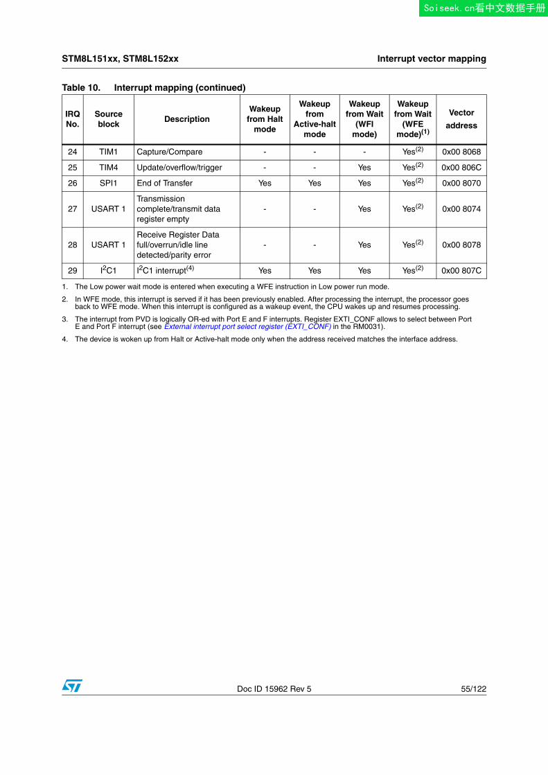
STM8L151xx, STM8L152xx Interrupt vector mapping
Doc ID 15962 Rev 5 55/122
24 TIM1 Capture/Compare - - - Yes(2) 0x00 8068
25 TIM4 Update/overflow/trigger - - Yes Yes(2) 0x00 806C
26 SPI1 End of Transfer Yes Yes Yes Yes(2) 0x00 8070
27 USART 1Transmission complete/transmit data register empty
- - Yes Yes(2) 0x00 8074
28 USART 1Receive Register Data full/overrun/idle line detected/parity error
- - Yes Yes(2) 0x00 8078
29 I2C1 I2C1 interrupt(4) Yes Yes Yes Yes(2) 0x00 807C
1. The Low power wait mode is entered when executing a WFE instruction in Low power run mode.
2. In WFE mode, this interrupt is served if it has been previously enabled. After processing the interrupt, the processor goes back to WFE mode. When this interrupt is configured as a wakeup event, the CPU wakes up and resumes processing.
3. The interrupt from PVD is logically OR-ed with Port E and F interrupts. Register EXTI_CONF allows to select between Port E and Port F interrupt (see External interrupt port select register (EXTI_CONF) in the RM0031).
4. The device is woken up from Halt or Active-halt mode only when the address received matches the interface address.
Table 10. Interrupt mapping (continued)
IRQNo.
Source block
DescriptionWakeup
from Halt mode
Wakeup from
Active-halt mode
Wakeup from Wait
(WFI mode)
Wakeup from Wait
(WFE mode)(1)
Vector
address
Soiseek.cn看中文数据手册
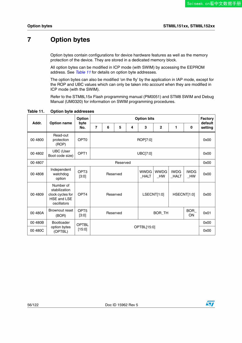
Option bytes STM8L151xx, STM8L152xx
56/122 Doc ID 15962 Rev 5
7 Option bytes
Option bytes contain configurations for device hardware features as well as the memory protection of the device. They are stored in a dedicated memory block.
All option bytes can be modified in ICP mode (with SWIM) by accessing the EEPROM address. See Table 11 for details on option byte addresses.
The option bytes can also be modified ‘on the fly’ by the application in IAP mode, except for the ROP and UBC values which can only be taken into account when they are modified in ICP mode (with the SWIM).
Refer to the STM8L15x Flash programming manual (PM0051) and STM8 SWIM and Debug Manual (UM0320) for information on SWIM programming procedures.
Table 11. Option byte addresses
Addr. Option nameOption
byte No.
Option bits Factory default setting7 6 5 4 3 2 1 0
00 4800Read-out protection
(ROP)OPT0 ROP[7:0] 0x00
00 4802 UBC (User
Boot code size)OPT1 UBC[7:0] 0x00
00 4807 Reserved 0x00
00 4808Independent
watchdog option
OPT3[3:0]
ReservedWWDG _HALT
WWDG _HW
IWDG _HALT
IWDG _HW
0x00
00 4809
Number of stabilization
clock cycles for HSE and LSE
oscillators
OPT4 Reserved LSECNT[1:0] HSECNT[1:0] 0x00
00 480ABrownout reset
(BOR)OPT5[3:0]
Reserved BOR_THBOR_
ON0x01
00 480B Bootloader option bytes
(OPTBL)
OPTBL [15:0]
OPTBL[15:0]0x00
00 480C 0x00
Soiseek.cn看中文数据手册
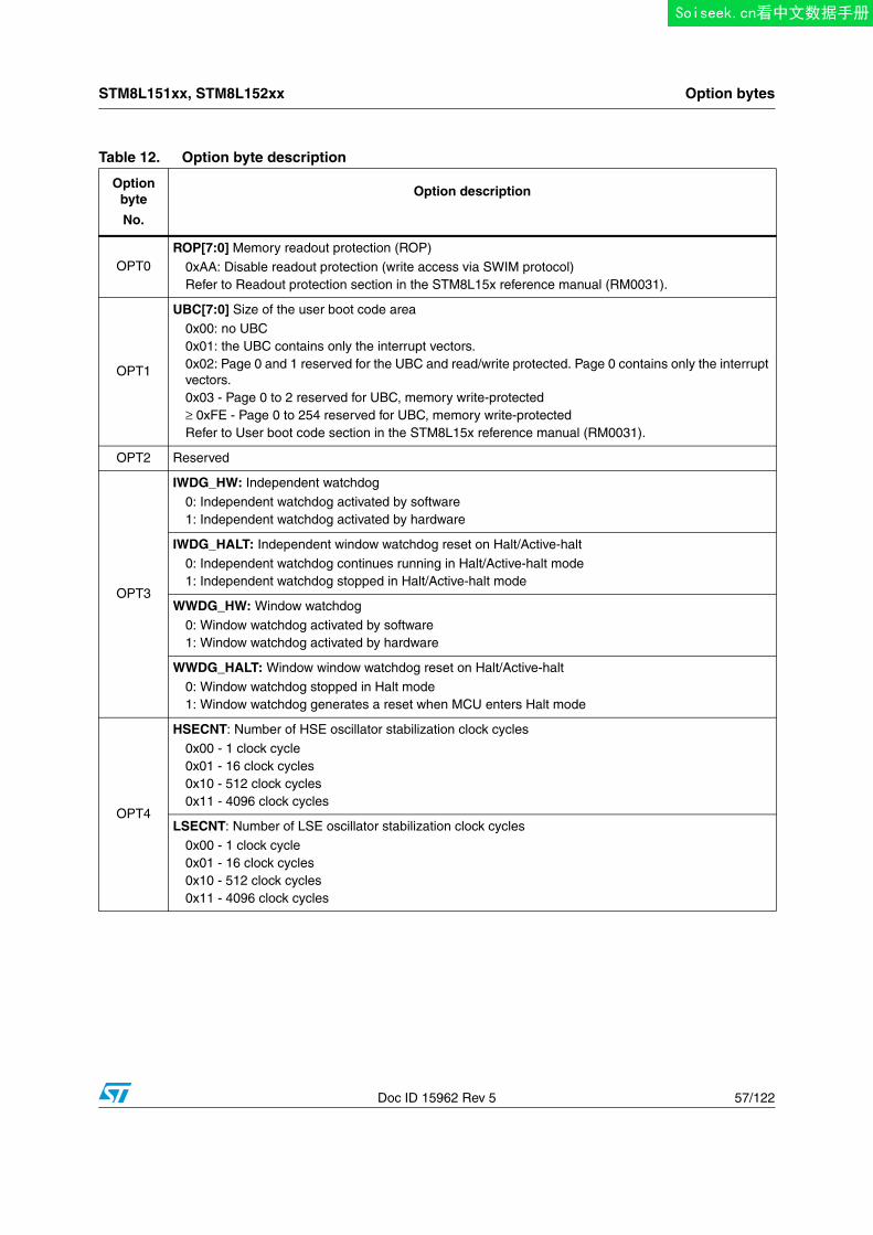
STM8L151xx, STM8L152xx Option bytes
Doc ID 15962 Rev 5 57/122
Table 12. Option byte description
Option byte
No.
Option description
OPT0ROP[7:0] Memory readout protection (ROP)
0xAA: Disable readout protection (write access via SWIM protocol)Refer to Readout protection section in the STM8L15x reference manual (RM0031).
OPT1
UBC[7:0] Size of the user boot code area
0x00: no UBC0x01: the UBC contains only the interrupt vectors.0x02: Page 0 and 1 reserved for the UBC and read/write protected. Page 0 contains only the interrupt vectors.0x03 - Page 0 to 2 reserved for UBC, memory write-protected≥ 0xFE - Page 0 to 254 reserved for UBC, memory write-protectedRefer to User boot code section in the STM8L15x reference manual (RM0031).
OPT2 Reserved
OPT3
IWDG_HW: Independent watchdog
0: Independent watchdog activated by software1: Independent watchdog activated by hardware
IWDG_HALT: Independent window watchdog reset on Halt/Active-halt
0: Independent watchdog continues running in Halt/Active-halt mode1: Independent watchdog stopped in Halt/Active-halt mode
WWDG_HW: Window watchdog
0: Window watchdog activated by software1: Window watchdog activated by hardware
WWDG_HALT: Window window watchdog reset on Halt/Active-halt
0: Window watchdog stopped in Halt mode1: Window watchdog generates a reset when MCU enters Halt mode
OPT4
HSECNT: Number of HSE oscillator stabilization clock cycles
0x00 - 1 clock cycle0x01 - 16 clock cycles0x10 - 512 clock cycles0x11 - 4096 clock cycles
LSECNT: Number of LSE oscillator stabilization clock cycles
0x00 - 1 clock cycle0x01 - 16 clock cycles0x10 - 512 clock cycles0x11 - 4096 clock cycles
Soiseek.cn看中文数据手册
Option bytes STM8L151xx, STM8L152xx
58/122 Doc ID 15962 Rev 5
OPT5
BOR_ON:
0: Brownout reset off1: Brownout reset on
BOR_TH[3:1]: Brownout reset thresholds. Refer to Table 18 for details on the thresholds according to the value of BOR_TH bits.
OPTBL
OPTBL[15:0]: This option is checked by the boot ROM code after reset. Depending on
content of addresses 00 480B, 00 480C and 0x8000 (reset vector) the
CPU jumps to the bootloader or to the reset vector.Refer to the UM0560 bootloader user manual for more details.
Table 12. Option byte description (continued)
Option byte
No.
Option description
Soiseek.cn看中文数据手册
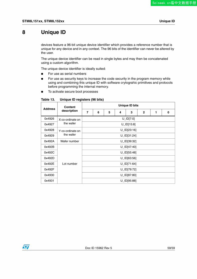
STM8L151xx, STM8L152xx Unique ID
Doc ID 15962 Rev 5 59/59
8 Unique ID
devices feature a 96-bit unique device identifier which provides a reference number that is unique for any device and in any context. The 96 bits of the identifier can never be altered by the user.
The unique device identifier can be read in single bytes and may then be concatenated using a custom algorithm.
The unique device identifier is ideally suited:
● For use as serial numbers
● For use as security keys to increase the code security in the program memory while using and combining this unique ID with software crytograhic primitives and protocols before programming the internal memory.
● To activate secure boot processes
Table 13. Unique ID registers (96 bits)
AddressContent
description
Unique ID bits
7 6 5 4 3 2 1 0
0x4926 X co-ordinate on the wafer
U_ID[7:0]
0x4927 U_ID[15:8]
0x4928 Y co-ordinate on the wafer
U_ID[23:16]
0x4929 U_ID[31:24]
0x492A Wafer number U_ID[39:32]
0x492B
Lot number
U_ID[47:40]
0x492C U_ID[55:48]
0x492D U_ID[63:56]
0x492E U_ID[71:64]
0x492F U_ID[79:72]
0x4930 U_ID[87:80]
0x4931 U_ID[95:88]
Soiseek.cn看中文数据手册
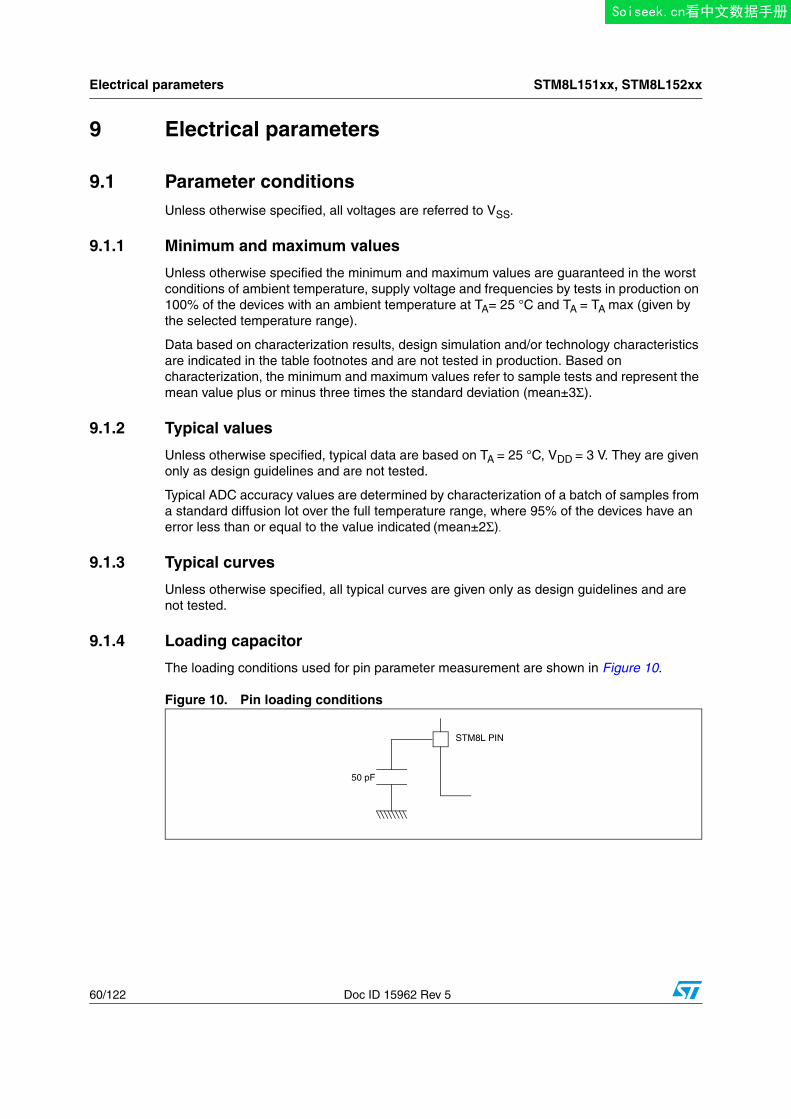
Electrical parameters STM8L151xx, STM8L152xx
60/122 Doc ID 15962 Rev 5
9 Electrical parameters
9.1 Parameter conditionsUnless otherwise specified, all voltages are referred to VSS.
9.1.1 Minimum and maximum values
Unless otherwise specified the minimum and maximum values are guaranteed in the worst conditions of ambient temperature, supply voltage and frequencies by tests in production on 100% of the devices with an ambient temperature at TA= 25 °C and TA = TA max (given by the selected temperature range).
Data based on characterization results, design simulation and/or technology characteristics are indicated in the table footnotes and are not tested in production. Based on characterization, the minimum and maximum values refer to sample tests and represent the mean value plus or minus three times the standard deviation (mean±3Σ).
9.1.2 Typical values
Unless otherwise specified, typical data are based on TA = 25 °C, VDD = 3 V. They are given only as design guidelines and are not tested.
Typical ADC accuracy values are determined by characterization of a batch of samples from a standard diffusion lot over the full temperature range, where 95% of the devices have an error less than or equal to the value indicated (mean±2Σ).
9.1.3 Typical curves
Unless otherwise specified, all typical curves are given only as design guidelines and are not tested.
9.1.4 Loading capacitor
The loading conditions used for pin parameter measurement are shown in Figure 10.
Figure 10. Pin loading conditions
50 pF
STM8L PIN
Soiseek.cn看中文数据手册
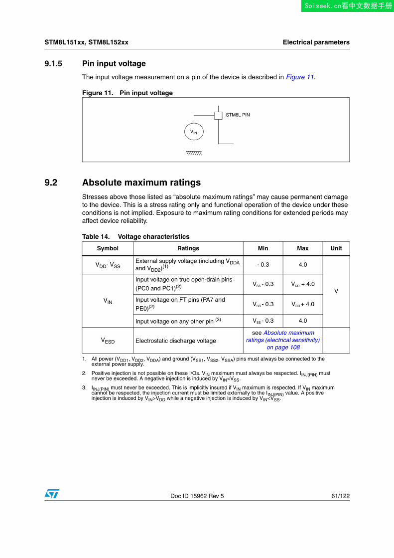
STM8L151xx, STM8L152xx Electrical parameters
Doc ID 15962 Rev 5 61/122
9.1.5 Pin input voltage
The input voltage measurement on a pin of the device is described in Figure 11.
Figure 11. Pin input voltage
9.2 Absolute maximum ratingsStresses above those listed as “absolute maximum ratings” may cause permanent damage to the device. This is a stress rating only and functional operation of the device under these conditions is not implied. Exposure to maximum rating conditions for extended periods may affect device reliability.
VIN
STM8L PIN
Table 14. Voltage characteristics
Symbol Ratings Min Max Unit
VDD- VSSExternal supply voltage (including VDDA and VDD2)(1)
1. All power (VDD1, VDD2, VDDA) and ground (VSS1, VSS2, VSSA) pins must always be connected to the external power supply.
- 0.3 4.0
V
VIN
Input voltage on true open-drain pins
(PC0 and PC1)(2) VSS - 0.3 VDD + 4.0
Input voltage on FT pins (PA7 and
PE0)(2)
2. Positive injection is not possible on these I/Os. VIN maximum must always be respected. IINJ(PIN) must never be exceeded. A negative injection is induced by VIN<VSS.
VSS - 0.3 VDD + 4.0
Input voltage on any other pin (3)
3. IINJ(PIN) must never be exceeded. This is implicitly insured if VIN maximum is respected. If VIN maximum cannot be respected, the injection current must be limited externally to the IINJ(PIN) value. A positive injection is induced by VIN>VDD while a negative injection is induced by VIN<VSS.
VSS - 0.3 4.0
VESD Electrostatic discharge voltage see Absolute maximum
ratings (electrical sensitivity) on page 108
Soiseek.cn看中文数据手册
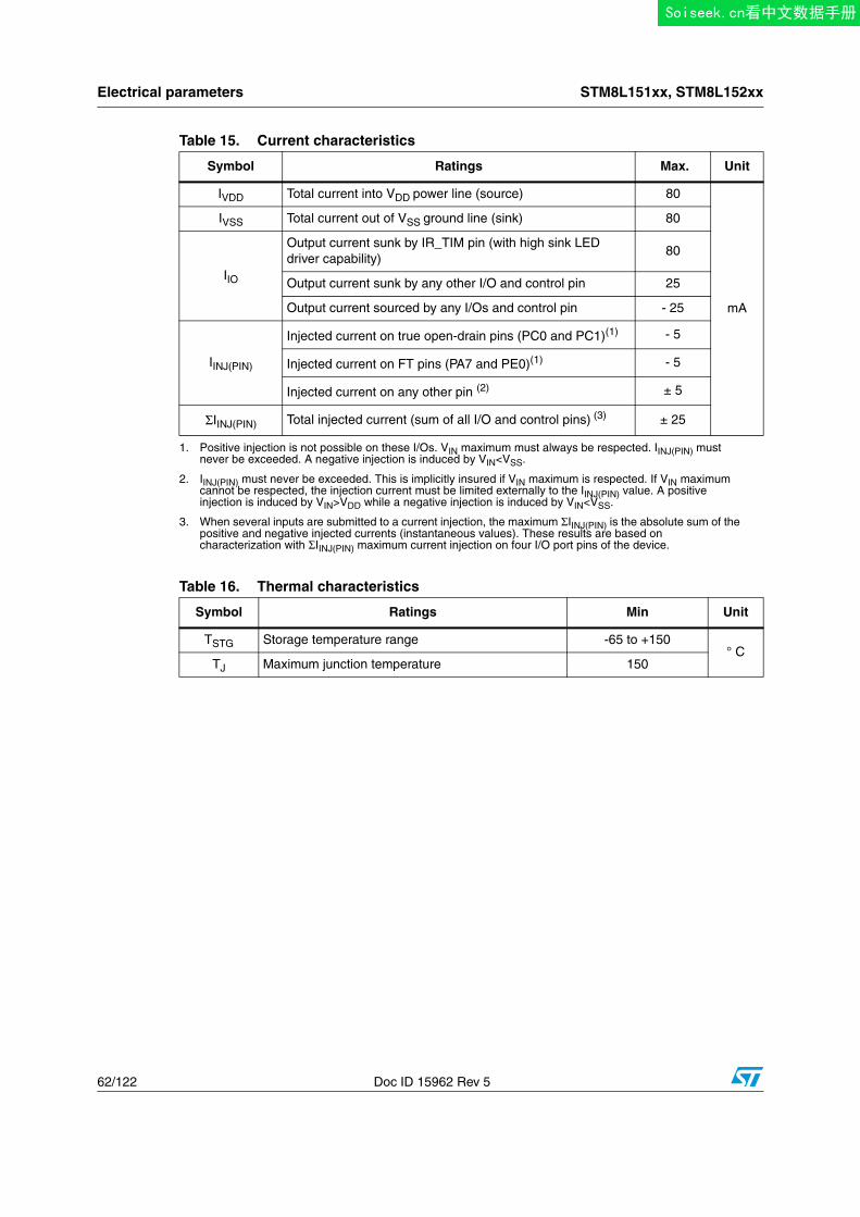
Electrical parameters STM8L151xx, STM8L152xx
62/122 Doc ID 15962 Rev 5
Table 15. Current characteristics
Symbol Ratings Max. Unit
IVDD Total current into VDD power line (source) 80
mA
IVSS Total current out of VSS ground line (sink) 80
IIO
Output current sunk by IR_TIM pin (with high sink LED driver capability)
80
Output current sunk by any other I/O and control pin 25
Output current sourced by any I/Os and control pin - 25
IINJ(PIN)
Injected current on true open-drain pins (PC0 and PC1)(1) - 5
Injected current on FT pins (PA7 and PE0)(1)
1. Positive injection is not possible on these I/Os. VIN maximum must always be respected. IINJ(PIN) must never be exceeded. A negative injection is induced by VIN<VSS.
- 5
Injected current on any other pin (2)
2. IINJ(PIN) must never be exceeded. This is implicitly insured if VIN maximum is respected. If VIN maximum cannot be respected, the injection current must be limited externally to the IINJ(PIN) value. A positive injection is induced by VIN>VDD while a negative injection is induced by VIN<VSS.
± 5
ΣIINJ(PIN) Total injected current (sum of all I/O and control pins) (3)
3. When several inputs are submitted to a current injection, the maximum ΣIINJ(PIN) is the absolute sum of the positive and negative injected currents (instantaneous values). These results are based on characterization with ΣIINJ(PIN) maximum current injection on four I/O port pins of the device.
± 25
Table 16. Thermal characteristics
Symbol Ratings Min Unit
TSTG Storage temperature range -65 to +150° C
TJ Maximum junction temperature 150
Soiseek.cn看中文数据手册
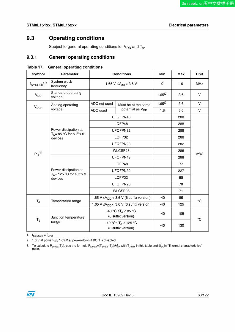
STM8L151xx, STM8L152xx Electrical parameters
Doc ID 15962 Rev 5 63/122
9.3 Operating conditionsSubject to general operating conditions for VDD and TA.
9.3.1 General operating conditions
Table 17. General operating conditions
Symbol Parameter Conditions Min Max Unit
fSYSCLK(1) System clock
frequency 1.65 V ≤ VDD < 3.6 V 0 16 MHz
VDDStandard operating voltage
1.65(2) 3.6 V
VDDAAnalog operating voltage
ADC not used Must be at the samepotential as VDD
1.65(2) 3.6 V
ADC used 1.8 3.6 V
PD(3)
Power dissipation at TA= 85 °C for suffix 6devices
UFQFPN48 288
mW
LQFP48 288
UFQFPN32 288
LQFP32 288
UFQFPN28 282
WLCSP28 286
Power dissipation atTA= 125 °C for suffix 3 devices
UFQFPN48 288
LQFP48 77
UFQFPN32 227
LQFP32 85
UFQFPN28 70
WLCSP28 71
TA Temperature range1.65 V ≤ VDD < 3.6 V (6 suffix version) -40 85
°C1.65 V ≤ VDD < 3.6 V (3 suffix version) -40 125
TJJunction temperature range
-40 °C ≤ TA < 85 °C
(6 suffix version)-40 105
°C-40 °C≤ TA < 125 °C
(3 suffix version)-40 130
1. fSYSCLK = fCPU
2. 1.8 V at power-up, 1.65 V at power-down if BOR is disabled
3. To calculate PDmax(TA), use the formula PDmax=(TJmax -TA)/ΘJA with TJmax in this table and ΘJA in “Thermal characteristics” table.
Soiseek.cn看中文数据手册
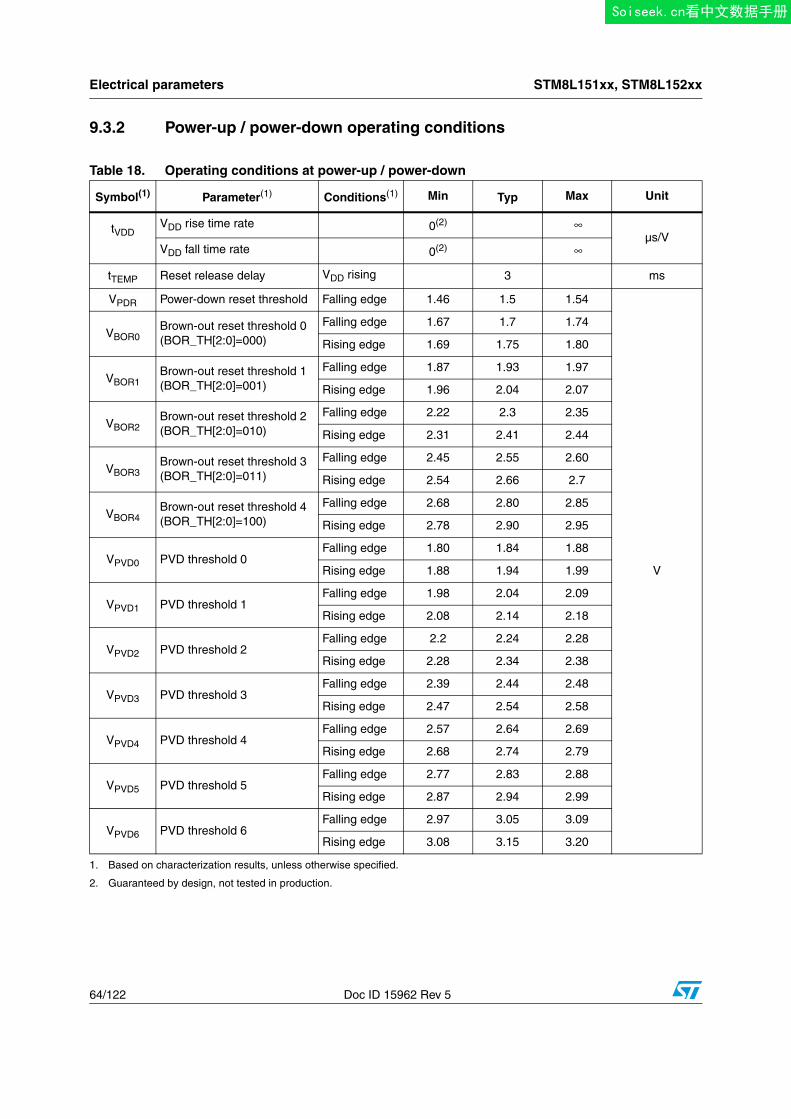
Electrical parameters STM8L151xx, STM8L152xx
64/122 Doc ID 15962 Rev 5
9.3.2 Power-up / power-down operating conditions
Table 18. Operating conditions at power-up / power-down
Symbol(1) Parameter(1) Conditions(1) Min Typ Max Unit
tVDDVDD rise time rate 0(2) ∞
µs/VVDD fall time rate 0(2) ∞
tTEMP Reset release delay VDD rising 3 ms
VPDR Power-down reset threshold Falling edge 1.46 1.5 1.54
V
VBOR0Brown-out reset threshold 0(BOR_TH[2:0]=000)
Falling edge 1.67 1.7 1.74
Rising edge 1.69 1.75 1.80
VBOR1Brown-out reset threshold 1(BOR_TH[2:0]=001)
Falling edge 1.87 1.93 1.97
Rising edge 1.96 2.04 2.07
VBOR2Brown-out reset threshold 2(BOR_TH[2:0]=010)
Falling edge 2.22 2.3 2.35
Rising edge 2.31 2.41 2.44
VBOR3Brown-out reset threshold 3(BOR_TH[2:0]=011)
Falling edge 2.45 2.55 2.60
Rising edge 2.54 2.66 2.7
VBOR4Brown-out reset threshold 4(BOR_TH[2:0]=100)
Falling edge 2.68 2.80 2.85
Rising edge 2.78 2.90 2.95
VPVD0 PVD threshold 0Falling edge 1.80 1.84 1.88
Rising edge 1.88 1.94 1.99
VPVD1 PVD threshold 1Falling edge 1.98 2.04 2.09
Rising edge 2.08 2.14 2.18
VPVD2 PVD threshold 2Falling edge 2.2 2.24 2.28
Rising edge 2.28 2.34 2.38
VPVD3 PVD threshold 3Falling edge 2.39 2.44 2.48
Rising edge 2.47 2.54 2.58
VPVD4 PVD threshold 4Falling edge 2.57 2.64 2.69
Rising edge 2.68 2.74 2.79
VPVD5 PVD threshold 5Falling edge 2.77 2.83 2.88
Rising edge 2.87 2.94 2.99
VPVD6 PVD threshold 6Falling edge 2.97 3.05 3.09
Rising edge 3.08 3.15 3.20
1. Based on characterization results, unless otherwise specified.
2. Guaranteed by design, not tested in production.
Soiseek.cn看中文数据手册
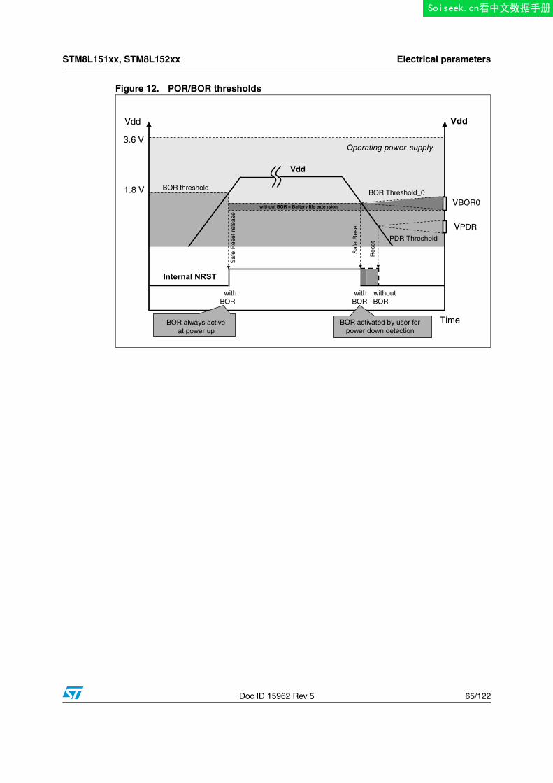
STM8L151xx, STM8L152xx Electrical parameters
Doc ID 15962 Rev 5 65/122
Figure 12. POR/BOR thresholds
Vdd
Internal NRST
Vdd
Operating power supply
Soiseek.cn看中文数据手册
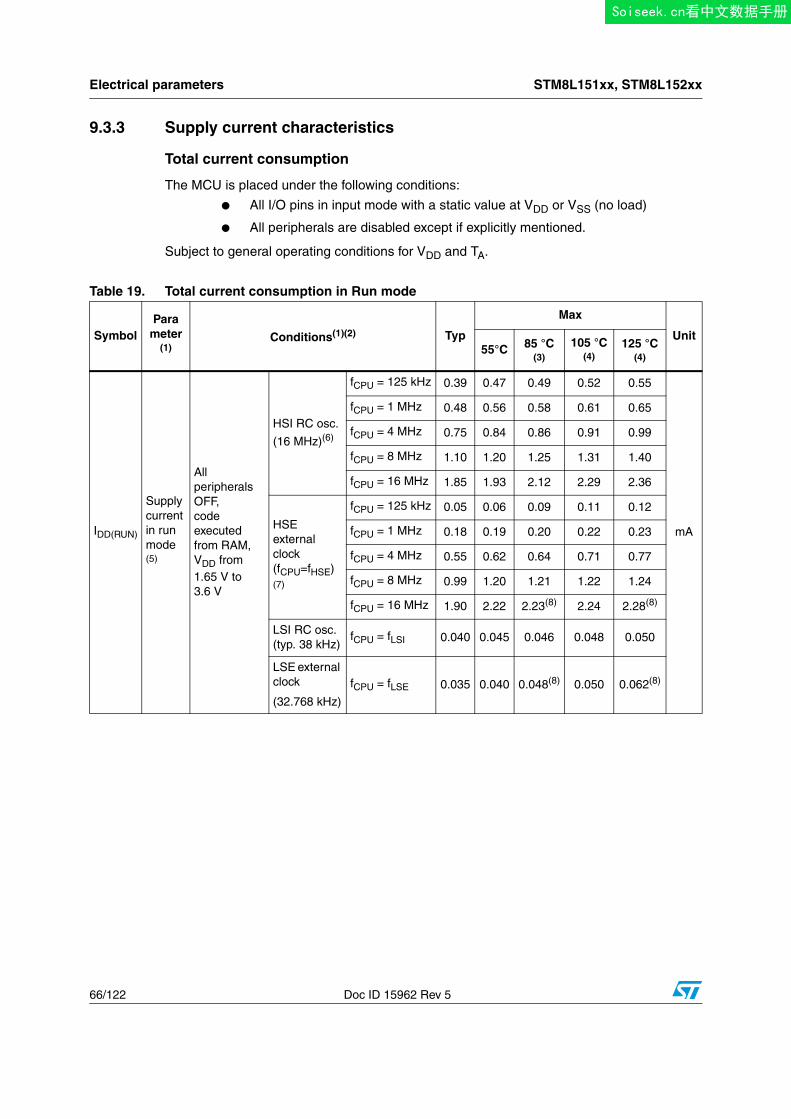
Electrical parameters STM8L151xx, STM8L152xx
66/122 Doc ID 15962 Rev 5
9.3.3 Supply current characteristics
Total current consumption
The MCU is placed under the following conditions:
● All I/O pins in input mode with a static value at VDD or VSS (no load)
● All peripherals are disabled except if explicitly mentioned.
Subject to general operating conditions for VDD and TA.
Table 19. Total current consumption in Run mode
SymbolPara
meter(1)
Conditions(1)(2) Typ
Max
Unit55°C 85 °C
(3)105 °C
(4)125 °C
(4)
IDD(RUN)
Supply current in run mode(5)
All peripherals OFF,code executedfrom RAM,VDD from 1.65 V to 3.6 V
HSI RC osc.
(16 MHz)(6)
fCPU = 125 kHz 0.39 0.47 0.49 0.52 0.55
mA
fCPU = 1 MHz 0.48 0.56 0.58 0.61 0.65
fCPU = 4 MHz 0.75 0.84 0.86 0.91 0.99
fCPU = 8 MHz 1.10 1.20 1.25 1.31 1.40
fCPU = 16 MHz 1.85 1.93 2.12 2.29 2.36
HSE external clock(fCPU=fHSE)(7)
fCPU = 125 kHz 0.05 0.06 0.09 0.11 0.12
fCPU = 1 MHz 0.18 0.19 0.20 0.22 0.23
fCPU = 4 MHz 0.55 0.62 0.64 0.71 0.77
fCPU = 8 MHz 0.99 1.20 1.21 1.22 1.24
fCPU = 16 MHz 1.90 2.22 2.23(8) 2.24 2.28(8)
LSI RC osc. (typ. 38 kHz)
fCPU = fLSI 0.040 0.045 0.046 0.048 0.050
LSE external clock
(32.768 kHz)
fCPU = fLSE 0.035 0.040 0.048(8) 0.050 0.062(8)
Soiseek.cn看中文数据手册
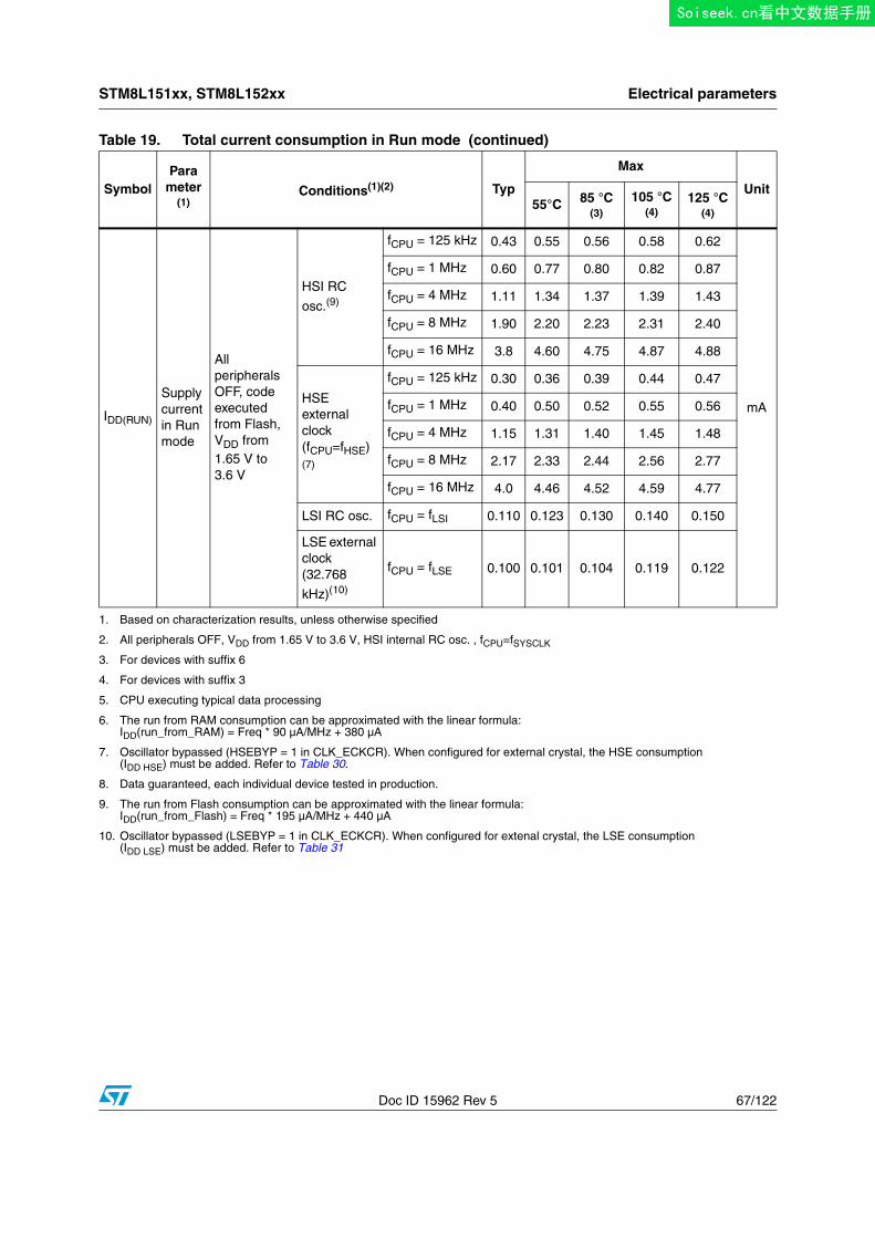
STM8L151xx, STM8L152xx Electrical parameters
Doc ID 15962 Rev 5 67/122
IDD(RUN)
Supply currentin Run mode
All peripherals OFF, code executed from Flash,VDD from 1.65 V to 3.6 V
HSI RC
osc.(9)
fCPU = 125 kHz 0.43 0.55 0.56 0.58 0.62
mA
fCPU = 1 MHz 0.60 0.77 0.80 0.82 0.87
fCPU = 4 MHz 1.11 1.34 1.37 1.39 1.43
fCPU = 8 MHz 1.90 2.20 2.23 2.31 2.40
fCPU = 16 MHz 3.8 4.60 4.75 4.87 4.88
HSE external clock (fCPU=fHSE) (7)
fCPU = 125 kHz 0.30 0.36 0.39 0.44 0.47
fCPU = 1 MHz 0.40 0.50 0.52 0.55 0.56
fCPU = 4 MHz 1.15 1.31 1.40 1.45 1.48
fCPU = 8 MHz 2.17 2.33 2.44 2.56 2.77
fCPU = 16 MHz 4.0 4.46 4.52 4.59 4.77
LSI RC osc. fCPU = fLSI 0.110 0.123 0.130 0.140 0.150
LSE external clock(32.768
kHz)(10)
fCPU = fLSE 0.100 0.101 0.104 0.119 0.122
1. Based on characterization results, unless otherwise specified
2. All peripherals OFF, VDD from 1.65 V to 3.6 V, HSI internal RC osc. , fCPU=fSYSCLK
3. For devices with suffix 6
4. For devices with suffix 3
5. CPU executing typical data processing
6. The run from RAM consumption can be approximated with the linear formula: IDD(run_from_RAM) = Freq * 90 µA/MHz + 380 µA
7. Oscillator bypassed (HSEBYP = 1 in CLK_ECKCR). When configured for external crystal, the HSE consumption (IDD HSE) must be added. Refer to Table 30.
8. Data guaranteed, each individual device tested in production.
9. The run from Flash consumption can be approximated with the linear formula: IDD(run_from_Flash) = Freq * 195 µA/MHz + 440 µA
10. Oscillator bypassed (LSEBYP = 1 in CLK_ECKCR). When configured for extenal crystal, the LSE consumption (IDD LSE) must be added. Refer to Table 31
Table 19. Total current consumption in Run mode (continued)
SymbolPara
meter(1)
Conditions(1)(2) Typ
Max
Unit55°C 85 °C
(3)105 °C
(4)125 °C
(4)
Soiseek.cn看中文数据手册
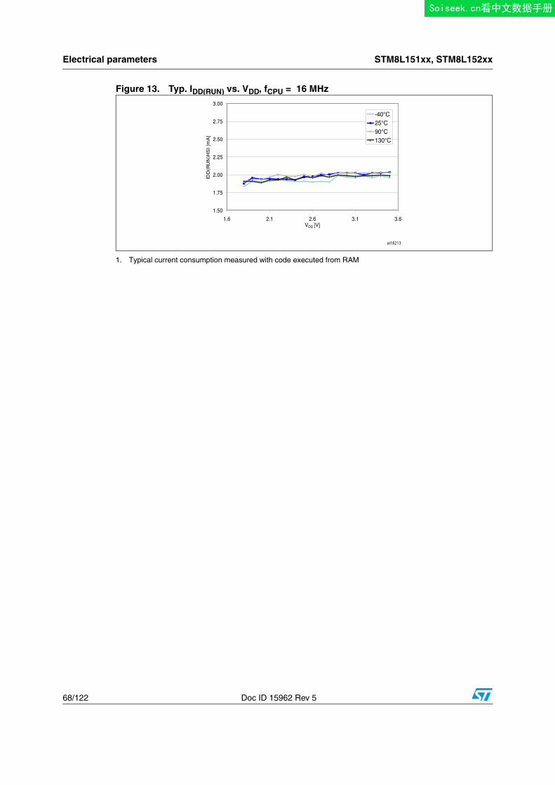
Electrical parameters STM8L151xx, STM8L152xx
68/122 Doc ID 15962 Rev 5
Figure 13. Typ. IDD(RUN) vs. VDD, fCPU = 16 MHz
1. Typical current consumption measured with code executed from RAM
Soiseek.cn看中文数据手册
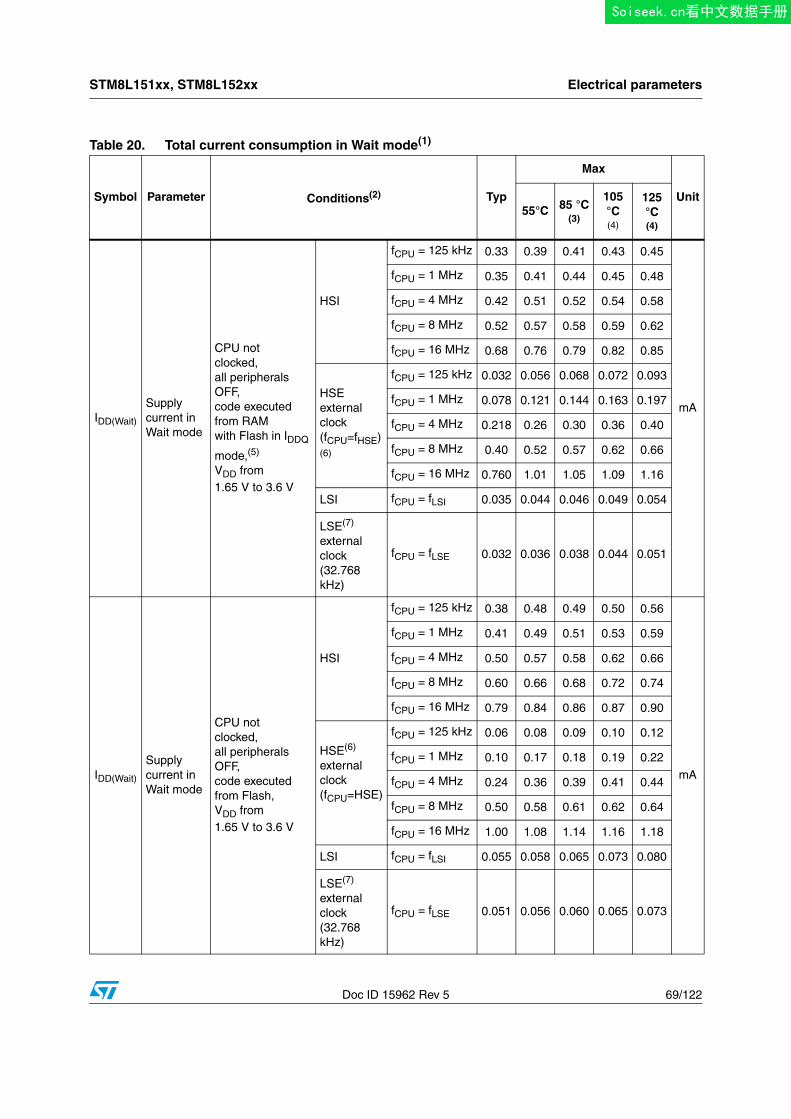
STM8L151xx, STM8L152xx Electrical parameters
Doc ID 15962 Rev 5 69/122
Table 20. Total current consumption in Wait mode(1)
Symbol Parameter Conditions(2) Typ
Max
Unit55°C 85 °C
(3)
105 °C(4)
125 °C(4)
IDD(Wait)
Supply current in Wait mode
CPU not clocked, all peripheralsOFF, code executed from RAM with Flash in IDDQ
mode,(5)
VDD from1.65 V to 3.6 V
HSI
fCPU = 125 kHz 0.33 0.39 0.41 0.43 0.45
mA
fCPU = 1 MHz 0.35 0.41 0.44 0.45 0.48
fCPU = 4 MHz 0.42 0.51 0.52 0.54 0.58
fCPU = 8 MHz 0.52 0.57 0.58 0.59 0.62
fCPU = 16 MHz 0.68 0.76 0.79 0.82 0.85
HSE external clock(fCPU=fHSE)(6)
fCPU = 125 kHz 0.032 0.056 0.068 0.072 0.093
fCPU = 1 MHz 0.078 0.121 0.144 0.163 0.197
fCPU = 4 MHz 0.218 0.26 0.30 0.36 0.40
fCPU = 8 MHz 0.40 0.52 0.57 0.62 0.66
fCPU = 16 MHz 0.760 1.01 1.05 1.09 1.16
LSI fCPU = fLSI 0.035 0.044 0.046 0.049 0.054
LSE(7) external clock(32.768kHz)
fCPU = fLSE 0.032 0.036 0.038 0.044 0.051
IDD(Wait)
Supply current in Wait mode
CPU notclocked, all peripheralsOFF, code executed from Flash,VDD from 1.65 V to 3.6 V
HSI
fCPU = 125 kHz 0.38 0.48 0.49 0.50 0.56
mA
fCPU = 1 MHz 0.41 0.49 0.51 0.53 0.59
fCPU = 4 MHz 0.50 0.57 0.58 0.62 0.66
fCPU = 8 MHz 0.60 0.66 0.68 0.72 0.74
fCPU = 16 MHz 0.79 0.84 0.86 0.87 0.90
HSE(6) external clock(fCPU=HSE)
fCPU = 125 kHz 0.06 0.08 0.09 0.10 0.12
fCPU = 1 MHz 0.10 0.17 0.18 0.19 0.22
fCPU = 4 MHz 0.24 0.36 0.39 0.41 0.44
fCPU = 8 MHz 0.50 0.58 0.61 0.62 0.64
fCPU = 16 MHz 1.00 1.08 1.14 1.16 1.18
LSI fCPU = fLSI 0.055 0.058 0.065 0.073 0.080
LSE(7) external clock(32.768kHz)
fCPU = fLSE 0.051 0.056 0.060 0.065 0.073
Soiseek.cn看中文数据手册
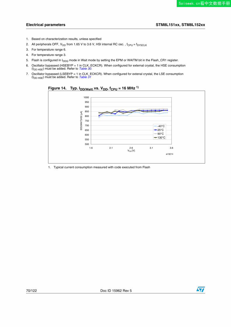
Electrical parameters STM8L151xx, STM8L152xx
70/122 Doc ID 15962 Rev 5
Figure 14. Typ. IDD(Wait) vs. VDD, fCPU = 16 MHz 1)
1. Typical current consumption measured with code executed from Flash
1. Based on characterization results, unless specified
2. All peripherals OFF, VDD from 1.65 V to 3.6 V, HSI internal RC osc. , fCPU = fSYSCLK
3. For temperature range 6.
4. For temperature range 3.
5. Flash is configured in IDDQ mode in Wait mode by setting the EPM or WAITM bit in the Flash_CR1 register.
6. Oscillator bypassed (HSEBYP = 1 in CLK_ECKCR). When configured for external crystal, the HSE consumption (IDD HSE) must be added. Refer to Table 30.
7. Oscillator bypassed (LSEBYP = 1 in CLK_ECKCR). When configured for extenal crystal, the LSE consumption (IDD HSE) must be added. Refer to Table 31
Soiseek.cn看中文数据手册
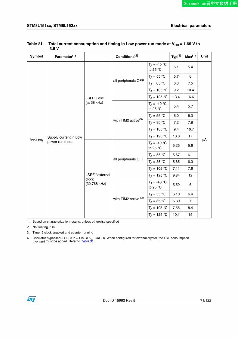
STM8L151xx, STM8L152xx Electrical parameters
Doc ID 15962 Rev 5 71/122
Table 21. Total current consumption and timing in Low power run mode at VDD = 1.65 V to 3.6 V
Symbol Parameter(1) Conditions(2) Typ(1) Max(1) Unit
IDD(LPR)Supply current in Low power run mode
LSI RC osc.(at 38 kHz)
all peripherals OFF
TA = -40 °C to 25 °C
5.1 5.4
μA
TA = 55 °C 5.7 6
TA = 85 °C 6.8 7.5
TA = 105 °C 9.2 10.4
TA = 125 °C 13.4 16.6
with TIM2 active(3)
TA = -40 °C to 25 °C
5.4 5.7
TA = 55 °C 6.0 6.3
TA = 85 °C 7.2 7.8
TA = 105 °C 9.4 10.7
TA = 125 °C 13.8 17
LSE (4) external clock(32.768 kHz)
all peripherals OFF
TA = -40 °C to 25 °C
5.25 5.6
TA = 55 °C 5.67 6.1
TA = 85 °C 5.85 6.3
TA = 105 °C 7.11 7.6
TA = 125 °C 9.84 12
with TIM2 active (3)
TA = -40 °C to 25 °C
5.59 6
TA = 55 °C 6.10 6.4
TA = 85 °C 6.30 7
TA = 105 °C 7.55 8.4
TA = 125 °C 10.1 15
1. Based on characterization results, unless otherwise specified
2. No floating I/Os
3. Timer 2 clock enabled and counter running
4. Oscillator bypassed (LSEBYP = 1 in CLK_ECKCR). When configured for extenal crystal, the LSE consumption (IDD LSE) must be added. Refer to Table 31
Soiseek.cn看中文数据手册
Electrical parameters STM8L151xx, STM8L152xx
72/122 Doc ID 15962 Rev 5
Figure 15. Typ. IDD(LPR) vs. VDD (LSI clock source)
0
2
4
6
8
10
12
14
16
18
1.6 2.1 2.6 3.1 3.6
VDD [V]
I DD
()L
SI [
µA]
-40°C
25°C
90°C
130°C
LPR
ai18216
Soiseek.cn看中文数据手册
STM8L151xx, STM8L152xx Electrical parameters
Doc ID 15962 Rev 5 73/122
Table 22. Total current consumption in Low power wait mode at VDD = 1.65 V to 3.6 V
Symbol Parameter(1)(2) ConditionsTyp(1)(2)
Max (1)(2) Unit
IDD(LPW)Supply current inLow power wait mode
LSI RC osc.(at 38 kHz)
all peripherals OFF
TA = -40 °C to 25 °C 3 3.3
μA
TA = 55 °C 3.3 3.6
TA = 85 °C 4.4 5
TA = 105 °C 6.7 8
TA = 125 °C 11 14
with TIM2 active(3)
TA = -40 °C to 25 °C 3.4 3.7
TA = 55 °C 3.7 4
TA = 85 °C 4.8 5.4
TA = 105 °C 7 8.3
TA = 125 °C 11.3 14.5
LSE external
clock(4)
(32.768 kHz)
all peripherals OFF
TA = -40 °C to 25 °C 2.35 2.7
TA = 55 °C 2.42 2.82
TA = 85 °C 3.10 3.71
TA = 105 °C 4.36 5.7
TA = 125 °C 7.20 11
with TIM2 active (3)
TA = -40 °C to 25 °C 2.46 2.75
TA = 55 °C 2.50 2.81
TA = 85 °C 3.16 3.82
TA = 105 °C 4.51 5.9
TA = 125 °C 7.28 11
1. No floating I/Os.
2. Based on characterization results, unless otherwise specified.
3. Timer 2 clock enabled and counter is running.
4. Oscillator bypassed (LSEBYP = 1 in CLK_ECKCR). When configured for extenal crystal, the LSE consumption (IDD LSE) must be added. Refer to Table 31.
Soiseek.cn看中文数据手册
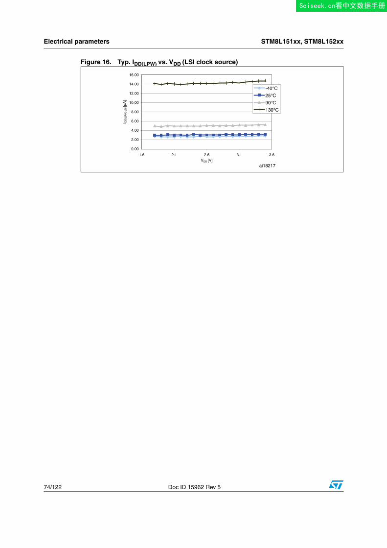
Electrical parameters STM8L151xx, STM8L152xx
74/122 Doc ID 15962 Rev 5
Figure 16. Typ. IDD(LPW) vs. VDD (LSI clock source)
0.00
2.00
4.00
6.00
8.00
10.00
12.00
14.00
16.00
1.6 2.1 2.6 3.1 3.6
VDD [V]
I DD
(LP
W )LS
I [µA
]
-40°C
25°C
90°C
130°C
ai18217
Soiseek.cn看中文数据手册
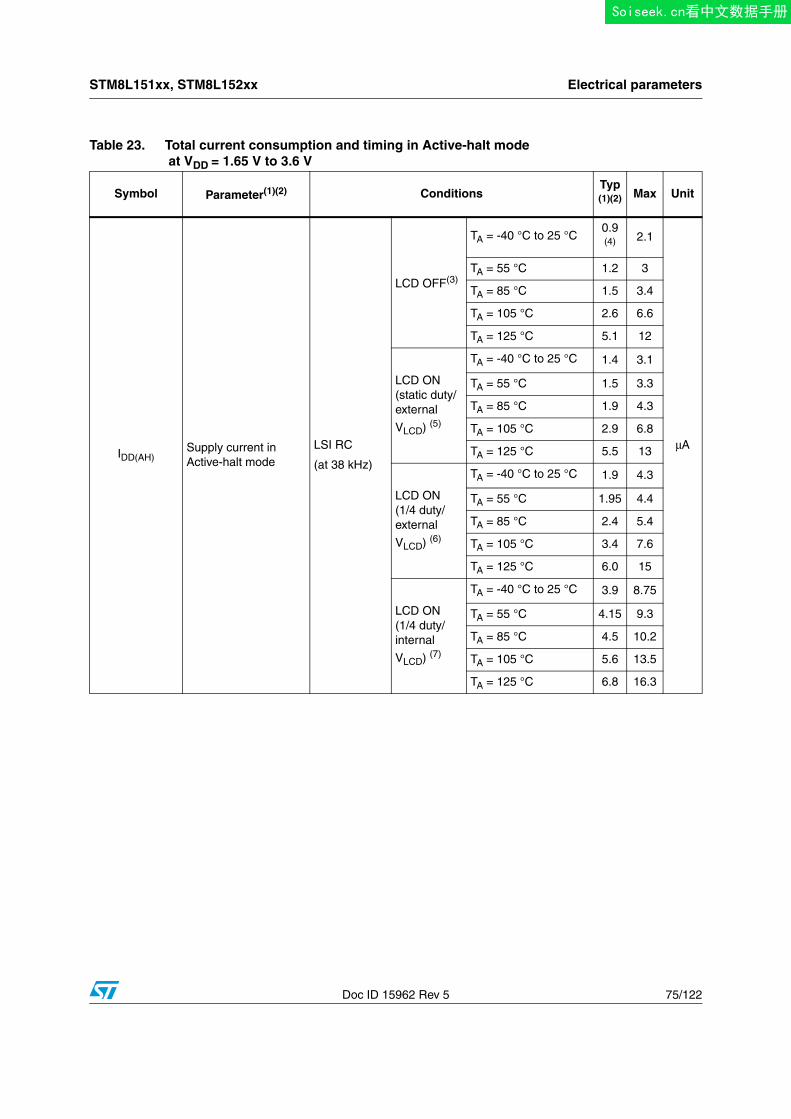
STM8L151xx, STM8L152xx Electrical parameters
Doc ID 15962 Rev 5 75/122
Table 23. Total current consumption and timing in Active-halt mode at VDD = 1.65 V to 3.6 V
Symbol Parameter(1)(2) ConditionsTyp(1)(2) Max Unit
IDD(AH)Supply current in Active-halt mode
LSI RC
(at 38 kHz)
LCD OFF(3)
TA = -40 °C to 25 °C0.9(4) 2.1
μA
TA = 55 °C 1.2 3
TA = 85 °C 1.5 3.4
TA = 105 °C 2.6 6.6
TA = 125 °C 5.1 12
LCD ON (static duty/external
VLCD) (5)
TA = -40 °C to 25 °C 1.4 3.1
TA = 55 °C 1.5 3.3
TA = 85 °C 1.9 4.3
TA = 105 °C 2.9 6.8
TA = 125 °C 5.5 13
LCD ON(1/4 duty/external
VLCD) (6)
TA = -40 °C to 25 °C 1.9 4.3
TA = 55 °C 1.95 4.4
TA = 85 °C 2.4 5.4
TA = 105 °C 3.4 7.6
TA = 125 °C 6.0 15
LCD ON(1/4 duty/internal
VLCD) (7)
TA = -40 °C to 25 °C 3.9 8.75
TA = 55 °C 4.15 9.3
TA = 85 °C 4.5 10.2
TA = 105 °C 5.6 13.5
TA = 125 °C 6.8 16.3
Soiseek.cn看中文数据手册
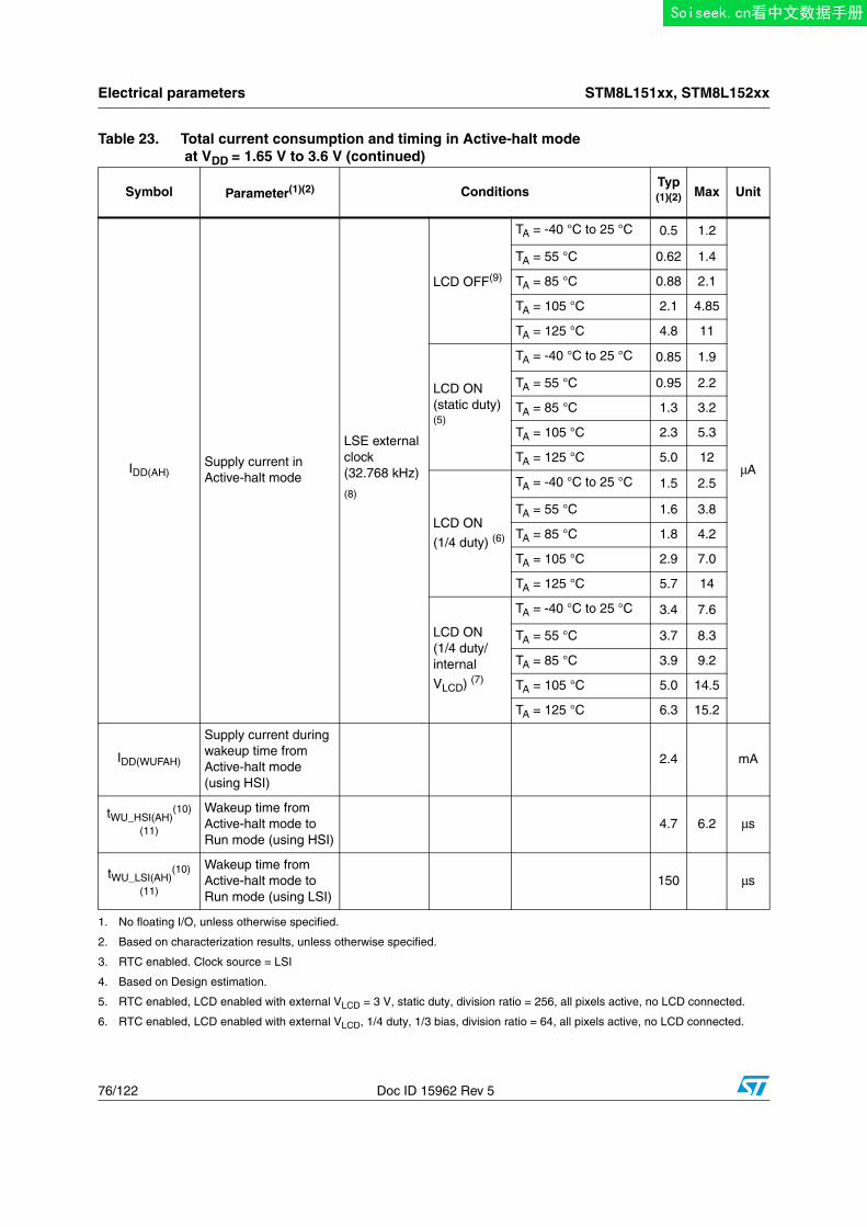
Electrical parameters STM8L151xx, STM8L152xx
76/122 Doc ID 15962 Rev 5
IDD(AH)Supply current in Active-halt mode
LSE external clock (32.768 kHz)
(8)
LCD OFF(9)
TA = -40 °C to 25 °C 0.5 1.2
μA
TA = 55 °C 0.62 1.4
TA = 85 °C 0.88 2.1
TA = 105 °C 2.1 4.85
TA = 125 °C 4.8 11
LCD ON (static duty) (5)
TA = -40 °C to 25 °C 0.85 1.9
TA = 55 °C 0.95 2.2
TA = 85 °C 1.3 3.2
TA = 105 °C 2.3 5.3
TA = 125 °C 5.0 12
LCD ON
(1/4 duty) (6)
TA = -40 °C to 25 °C 1.5 2.5
TA = 55 °C 1.6 3.8
TA = 85 °C 1.8 4.2
TA = 105 °C 2.9 7.0
TA = 125 °C 5.7 14
LCD ON(1/4 duty/internal
VLCD) (7)
TA = -40 °C to 25 °C 3.4 7.6
TA = 55 °C 3.7 8.3
TA = 85 °C 3.9 9.2
TA = 105 °C 5.0 14.5
TA = 125 °C 6.3 15.2
IDD(WUFAH)
Supply current during wakeup time from Active-halt mode(using HSI)
2.4 mA
tWU_HSI(AH)(10)
(11)
Wakeup time from Active-halt mode to Run mode (using HSI)
4.7 6.2 μs
tWU_LSI(AH)(10)
(11)
Wakeup time from Active-halt mode to Run mode (using LSI)
150 μs
1. No floating I/O, unless otherwise specified.
2. Based on characterization results, unless otherwise specified.
3. RTC enabled. Clock source = LSI
4. Based on Design estimation.
5. RTC enabled, LCD enabled with external VLCD = 3 V, static duty, division ratio = 256, all pixels active, no LCD connected.
6. RTC enabled, LCD enabled with external VLCD, 1/4 duty, 1/3 bias, division ratio = 64, all pixels active, no LCD connected.
Table 23. Total current consumption and timing in Active-halt mode at VDD = 1.65 V to 3.6 V (continued)
Symbol Parameter(1)(2) ConditionsTyp(1)(2) Max Unit
Soiseek.cn看中文数据手册
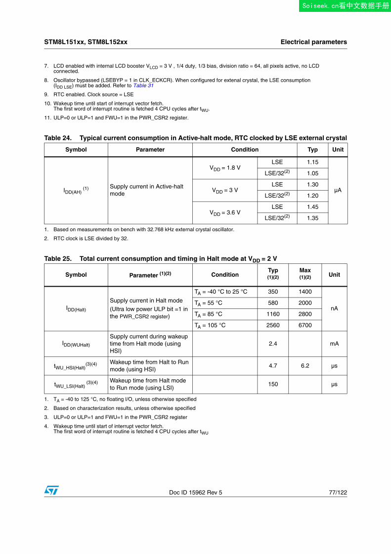
STM8L151xx, STM8L152xx Electrical parameters
Doc ID 15962 Rev 5 77/122
7. LCD enabled with internal LCD booster VLCD = 3 V , 1/4 duty, 1/3 bias, division ratio = 64, all pixels active, no LCD connected.
8. Oscillator bypassed (LSEBYP = 1 in CLK_ECKCR). When configured for extenal crystal, the LSE consumption (IDD LSE) must be added. Refer to Table 31
9. RTC enabled. Clock source = LSE
10. Wakeup time until start of interrupt vector fetch. The first word of interrupt routine is fetched 4 CPU cycles after tWU.
11. ULP=0 or ULP=1 and FWU=1 in the PWR_CSR2 register.
Table 24. Typical current consumption in Active-halt mode, RTC clocked by LSE external crystal
Symbol Parameter Condition Typ Unit
IDD(AH) (1) Supply current in Active-halt
mode
VDD = 1.8 VLSE 1.15
µA
LSE/32(2) 1.05
VDD = 3 VLSE 1.30
LSE/32(2) 1.20
VDD = 3.6 VLSE 1.45
LSE/32(2) 1.35
1. Based on measurements on bench with 32.768 kHz external crystal oscillator.
2. RTC clock is LSE divided by 32.
Table 25. Total current consumption and timing in Halt mode at VDD = 2 V
Symbol Parameter (1)(2) ConditionTyp(1)(2)
Max (1)(2) Unit
IDD(Halt)
Supply current in Halt mode
(Ultra low power ULP bit =1 in the PWR_CSR2 register)
TA = -40 °C to 25 °C 350 1400
nATA = 55 °C 580 2000
TA = 85 °C 1160 2800
TA = 105 °C 2560 6700
IDD(WUHalt)
Supply current during wakeup time from Halt mode (using HSI)
2.4 mA
tWU_HSI(Halt)(3)(4) Wakeup time from Halt to Run
mode (using HSI)4.7 6.2 µs
tWU_LSI(Halt) (3)(4) Wakeup time from Halt mode
to Run mode (using LSI)150 µs
1. TA = -40 to 125 °C, no floating I/O, unless otherwise specified
2. Based on characterization results, unless otherwise specified
3. ULP=0 or ULP=1 and FWU=1 in the PWR_CSR2 register
4. Wakeup time until start of interrupt vector fetch. The first word of interrupt routine is fetched 4 CPU cycles after tWU
Soiseek.cn看中文数据手册
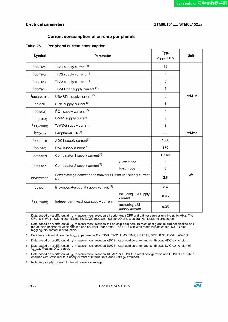
Electrical parameters STM8L151xx, STM8L152xx
78/122 Doc ID 15962 Rev 5
Current consumption of on-chip peripherals
Table 26. Peripheral current consumption
Symbol ParameterTyp.
VDD = 3.0 VUnit
IDD(TIM1) TIM1 supply current(1) 13
µA/MHz
IDD(TIM2) TIM2 supply current (1) 8
IDD(TIM3) TIM3 supply current (1) 8
IDD(TIM4) TIM4 timer supply current (1) 3
IDD(USART1) USART1 supply current (2) 6
IDD(SPI1) SPI1 supply current (2) 3
IDD(I2C1) I2C1 supply current (2) 5
IDD(DMA1) DMA1 supply current 3
IDD(WWDG) WWDG supply current 2
IDD(ALL) Peripherals ON(3) 44 µA/MHz
IDD(ADC1) ADC1 supply current(4) 1500
µA
IDD(DAC) DAC supply current(5) 370
IDD(COMP1) Comparator 1 supply current(6) 0.160
IDD(COMP2) Comparator 2 supply current(6)Slow mode 2
Fast mode 5
IDD(PVD/BOR)Power voltage detector and brownout Reset unit supply current (7) 2.6
IDD(BOR) Brownout Reset unit supply current (7) 2.4
IDD(IDWDG) Independent watchdog supply current
including LSI supply current
0.45
excluding LSI supply current
0.05
1. Data based on a differential IDD measurement between all peripherals OFF and a timer counter running at 16 MHz. The CPU is in Wait mode in both cases. No IC/OC programmed, no I/O pins toggling. Not tested in production.
2. Data based on a differential IDD measurement between the on-chip peripheral in reset configuration and not clocked and the on-chip peripheral when clocked and not kept under reset. The CPU is in Wait mode in both cases. No I/O pins toggling. Not tested in production.
3. Peripherals listed above the IDD(ALL) parameter ON: TIM1, TIM2, TIM3, TIM4, USART1, SPI1, I2C1, DMA1, WWDG.
4. Data based on a differential IDD measurement between ADC in reset configuration and continuous ADC conversion.
5. Data based on a differential IDD measurement between DAC in reset configuration and continuous DAC conversion of VDD /2. Floating DAC output.
6. Data based on a differential IDD measurement between COMP1 or COMP2 in reset configuration and COMP1 or COMP2 enabled with static inputs. Supply current of internal reference voltage excluded.
7. Including supply current of internal reference voltage.
Soiseek.cn看中文数据手册
STM8L151xx, STM8L152xx Electrical parameters
Doc ID 15962 Rev 5 79/122
9.3.4 Clock and timing characteristics
HSE external clock (HSEBYP = 1 in CLK_ECKCR)
Subject to general operating conditions for VDD and TA.
LSE external clock (LSEBYP=1 in CLK_ECKCR)
Subject to general operating conditions for VDD and TA.
Table 27. Current consumption under external reset
Symbol Parameter Conditions Typ Unit
IDD(RST)Supply current under
external reset (1)All pins are externally tied to VDD
VDD = 1.8 V 48
µAVDD = 3 V 76
VDD = 3.6 V 91
1. All pins except PA0, PB0 and PB4 are floating under reset. PA0, PB0 and PB4 are configured with pull-up under reset.
Table 28. HSE external clock characteristics
Symbol Parameter Conditions Min Typ Max Unit
fHSE_extExternal clock source
frequency(1)
1. Guaranteed by design, not tested in production.
1 16 MHz
VHSEH(2)
2. Data based on characterization results, not tested in production.
OSC_IN input pin high level voltage
0.7 x VDD VDD
V
VHSEL(2) OSC_IN input pin low level
voltageVSS 0.3 x VDD
Cin(HSE)OSC_IN input
capacitance(1) 2.6 pF
ILEAK_HSEOSC_IN input leakage current
VSS < VIN < VDD ±1 µA
Table 29. LSE external clock characteristics
Symbol Parameter Min Typ Max Unit
fLSE_ext External clock source frequency(1) 32.768 kHz
VLSEH(2) OSC32_IN input pin high level voltage 0.7 x VDD VDD
VVLSEL
(2) OSC32_IN input pin low level voltage VSS 0.3 x VDD
Cin(LSE) OSC32_IN input capacitance(1) 0.6 pF
ILEAK_LSE OSC32_IN input leakage current ±1 µA
1. Guaranteed by design, not tested in production.
2. Data based on characterization results, not tested in production.
Soiseek.cn看中文数据手册
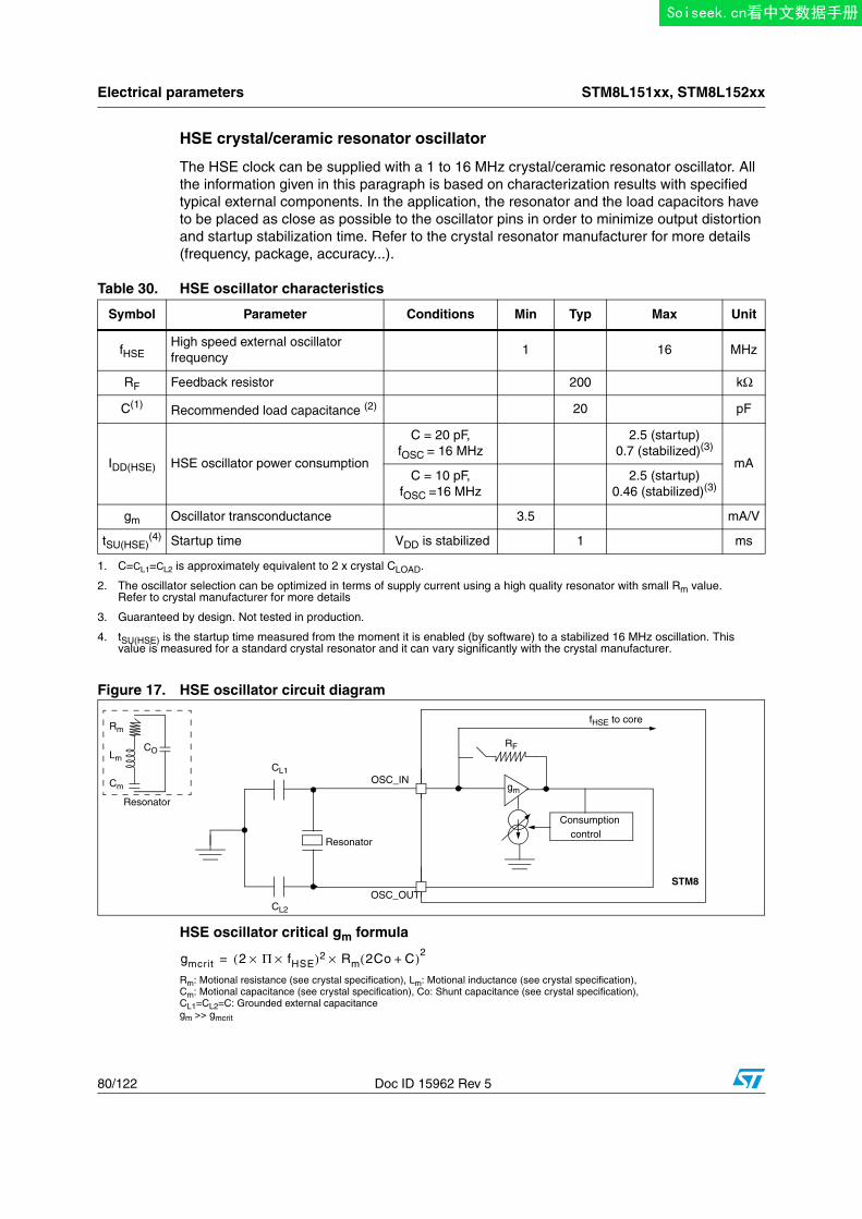
Electrical parameters STM8L151xx, STM8L152xx
80/122 Doc ID 15962 Rev 5
HSE crystal/ceramic resonator oscillator
The HSE clock can be supplied with a 1 to 16 MHz crystal/ceramic resonator oscillator. All the information given in this paragraph is based on characterization results with specified typical external components. In the application, the resonator and the load capacitors have to be placed as close as possible to the oscillator pins in order to minimize output distortion and startup stabilization time. Refer to the crystal resonator manufacturer for more details (frequency, package, accuracy...).
Figure 17. HSE oscillator circuit diagram
HSE oscillator critical gm formula
Rm: Motional resistance (see crystal specification), Lm: Motional inductance (see crystal specification),Cm: Motional capacitance (see crystal specification), Co: Shunt capacitance (see crystal specification),CL1=CL2=C: Grounded external capacitancegm >> gmcrit
Table 30. HSE oscillator characteristics
Symbol Parameter Conditions Min Typ Max Unit
fHSEHigh speed external oscillator frequency
1 16 MHz
RF Feedback resistor 200 kΩ
C(1) Recommended load capacitance (2) 20 pF
IDD(HSE) HSE oscillator power consumption
C = 20 pF,fOSC = 16 MHz
2.5 (startup)0.7 (stabilized)(3)
mAC = 10 pF,
fOSC =16 MHz2.5 (startup)
0.46 (stabilized)(3)
gm Oscillator transconductance 3.5 mA/V
tSU(HSE)(4) Startup time VDD is stabilized 1 ms
1. C=CL1=CL2 is approximately equivalent to 2 x crystal CLOAD.
2. The oscillator selection can be optimized in terms of supply current using a high quality resonator with small Rm value. Refer to crystal manufacturer for more details
3. Guaranteed by design. Not tested in production.
4. tSU(HSE) is the startup time measured from the moment it is enabled (by software) to a stabilized 16 MHz oscillation. This value is measured for a standard crystal resonator and it can vary significantly with the crystal manufacturer.
OSC_OUT
OSC_IN
fHSE to core
CL1
CL2
RF
STM8
Resonator
Consumption control
gm
Rm
Cm
LmCO
Resonator
gmcrit 2 Π× fHSE×( )2 Rm× 2Co C+( )2=
Soiseek.cn看中文数据手册
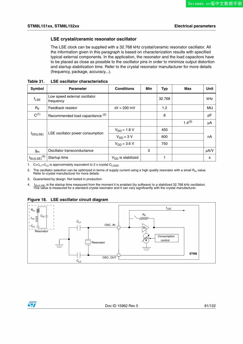
STM8L151xx, STM8L152xx Electrical parameters
Doc ID 15962 Rev 5 81/122
LSE crystal/ceramic resonator oscillator
The LSE clock can be supplied with a 32.768 kHz crystal/ceramic resonator oscillator. All the information given in this paragraph is based on characterization results with specified typical external components. In the application, the resonator and the load capacitors have to be placed as close as possible to the oscillator pins in order to minimize output distortion and startup stabilization time. Refer to the crystal resonator manufacturer for more details (frequency, package, accuracy...).
Figure 18. LSE oscillator circuit diagram
Table 31. LSE oscillator characteristics
Symbol Parameter Conditions Min Typ Max Unit
fLSELow speed external oscillator frequency
32.768 kHz
RF Feedback resistor ΔV = 200 mV 1.2 MΩ
C(1) Recommended load capacitance (2) 8 pF
IDD(LSE) LSE oscillator power consumption
1.4(3) µA
VDD = 1.8 V 450
nAVDD = 3 V 600
VDD = 3.6 V 750
gm Oscillator transconductance 3 µA/V
tSU(LSE)(4) Startup time VDD is stabilized 1 s
1. C=CL1=CL2 is approximately equivalent to 2 x crystal CLOAD.
2. The oscillator selection can be optimized in terms of supply current using a high quality resonator with a small Rm value. Refer to crystal manufacturer for more details.
3. Guaranteed by design. Not tested in production.
4. tSU(LSE) is the startup time measured from the moment it is enabled (by software) to a stabilized 32.768 kHz oscillation. This value is measured for a standard crystal resonator and it can vary significantly with the crystal manufacturer.
OSC_OUT
OSC_IN
fLSE
CL1
CL2
RF
STM8
Resonator
Consumption control
gm
Rm
Cm
LmCO
Resonator
Soiseek.cn看中文数据手册
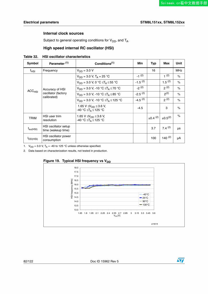
Electrical parameters STM8L151xx, STM8L152xx
82/122 Doc ID 15962 Rev 5
Internal clock sources
Subject to general operating conditions for VDD, and TA.
High speed internal RC oscillator (HSI)
Figure 19. Typical HSI frequency vs VDD
Table 32. HSI oscillator characteristics
Symbol Parameter (1) Conditions(1) Min Typ Max Unit
fHSI Frequency VDD = 3.0 V 16 MHz
ACCHSIAccuracy of HSI oscillator (factory calibrated)
VDD = 3.0 V, TA = 25 °C -1 (2) 1 (2) %
VDD = 3.0 V, 0 °C ≤ TA ≤ 55 °C -1.5 (2) 1.5 (2) %
VDD = 3.0 V, -10 °C ≤ TA ≤ 70 °C -2 (2) 2 (2) %
VDD = 3.0 V, -10 °C ≤ TA ≤ 85 °C -2.5 (2) 2(2) %
VDD = 3.0 V, -10 °C ≤ TA ≤ 125 °C -4.5 (2) 2 (2) %
1.65 V ≤ VDD ≤ 3.6 V,-40 °C ≤ TA ≤ 125 °C
-4.5 3 %
TRIMHSI user trim resolution
1.65 V ≤ VDD ≤ 3.6 V,-40 °C ≤ TA ≤ 125 °C
±0.4 (2) ±0.5(2) %
tsu(HSI)HSI oscillator setup time (wakeup time)
3.7 7.4 (2) µs
IDD(HSI)HSI oscillator power consumption
100 140 (2) µA
1. VDD = 3.0 V, TA = -40 to 125 °C unless otherwise specified.
2. Data based on characterization results, not tested in production.
Soiseek.cn看中文数据手册
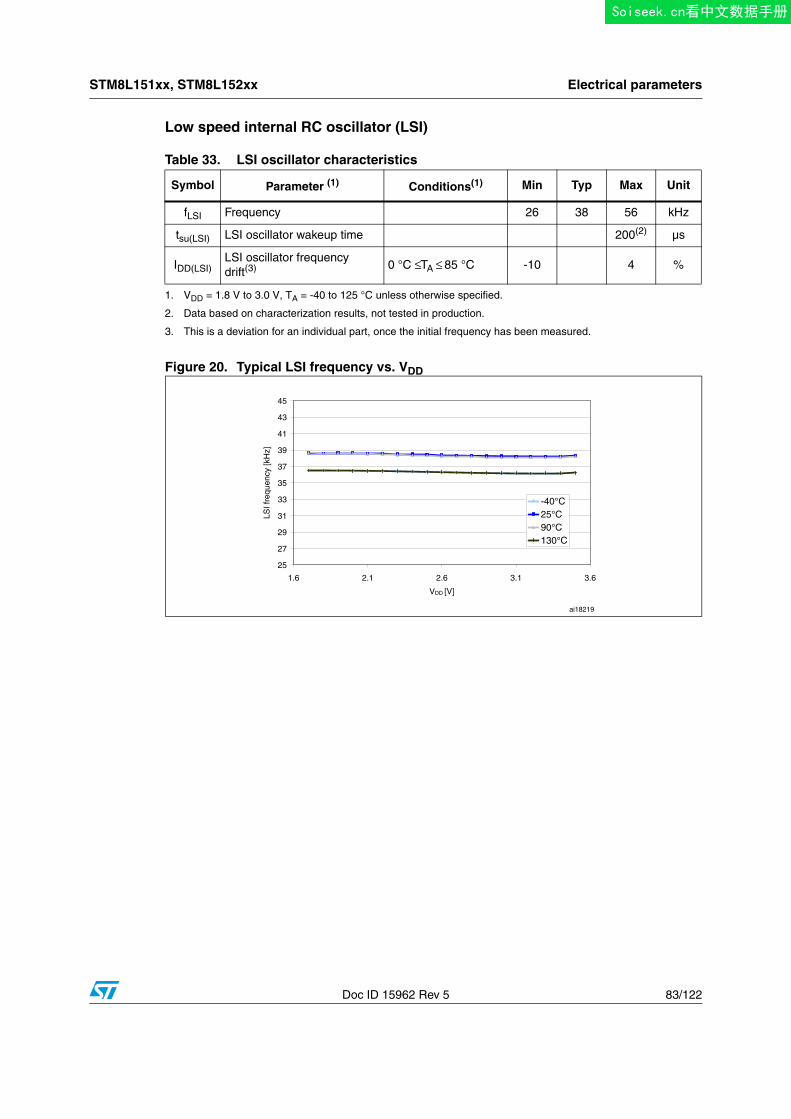
STM8L151xx, STM8L152xx Electrical parameters
Doc ID 15962 Rev 5 83/122
Low speed internal RC oscillator (LSI)
Figure 20. Typical LSI frequency vs. VDD
Table 33. LSI oscillator characteristics
Symbol Parameter (1)
1. VDD = 1.8 V to 3.0 V, TA = -40 to 125 °C unless otherwise specified.
Conditions(1) Min Typ Max Unit
fLSI Frequency 26 38 56 kHz
tsu(LSI) LSI oscillator wakeup time 200(2)
2. Data based on characterization results, not tested in production.
µs
IDD(LSI)LSI oscillator frequency drift(3)
3. This is a deviation for an individual part, once the initial frequency has been measured.
0 °C ≤ TA ≤ 85 °C -10 4 %
Soiseek.cn看中文数据手册
Electrical parameters STM8L151xx, STM8L152xx
84/122 Doc ID 15962 Rev 5
9.3.5 Memory characteristics
TA = -40 to 125 °C unless otherwise specified.
Table 34. RAM and hardware registers
Symbol Parameter Conditions Min Typ Max Unit
VRM Data retention mode (1)
1. Minimum supply voltage without losing data stored in RAM (in Halt mode or under Reset) or in hardware registers (only in Halt mode). Guaranteed by characterization, not tested in production.
Flash memory
Halt mode (or Reset) 1.4 V
Table 35. Flash program and data EEPROM memory
Symbol Parameter Conditions Min TypMax
(1) Unit
VDDOperating voltage (all modes, read/write/erase)
fSYSCLK = 16 MHz 1.65 3.6 V
tprog
Programming time for 1 or 128 bytes (block) erase/write cycles (on programmed byte)
6 ms
Programming time for 1 to 128 bytes (block) write cycles (on erased byte)
3 ms
Iprog Programming/ erasing consumptionTA=+25 °C, VDD = 3.0 V
0.7 mATA=+25 °C, VDD = 1.8 V
tRET
Data retention (program memory) after 10000 erase/write cycles at TA=+85 °C
TRET=+55 °C 20(1)
yearsData retention (data memory) after 10000 erase/write cycles at TA=+85 °C
TRET=+55 °C 20(1)
Data retention (data memory) after 10000 erase/write cycles at TA=+85 °C
TRET=+85 °C 1(1)
NRW
Erase/write cycles (program memory) See notes (1)(2) 10(1)
kcyclesErase/write cycles (data memory) See notes (1)(3) 300(1)
(4)
1. Data based on characterization results, not tested in production.
2. Retention guaranteed after cycling is 10 years @ 55 °C.
3. Retention guaranteed after cycling is 1 year @ 55 °C.
4. Data based on characterization performed on the whole data memory.
Soiseek.cn看中文数据手册
STM8L151xx, STM8L152xx Electrical parameters
Doc ID 15962 Rev 5 85/122
9.3.6 I/O port pin characteristics
General characteristics
Subject to general operating conditions for VDD and TA unless otherwise specified. All unused pins must be kept at a fixed voltage: using the output mode of the I/O for example or an external pull-up or pull-down resistor.
Table 36. I/O static characteristics
Symbol Parameter(1) Conditions(1) Min Typ Max Unit
VIL Input low level voltage(2)
Input voltage on true open-drain pins (PC0 and PC1)
VSS -0.3 0.3 x VDD
VInput voltage on FT pins (PA7 and PE0)
VSS -0.3 0.3 x VDD
Input voltage on any other pin
VSS -0.3 0.3 x VDD
VIH Input high level voltage (2)
Input voltage on true open-drain pins (PC0 and PC1) with VDD < 2 V
0.70 x VDD
5.2
V
Input voltage on true open-drain pins (PC0 and PC1) with VDD ≥ 2 V
5.5
Input voltage on FT pins (PA7 and PE0)with VDD < 2 V
0.70 x VDD
5.2
Input voltage on FT pins (PA7 and PE0)with VDD ≥ 2 V
5.5
Input voltage on any other pin
0.70 x VDD VDD+0.3
Vhys Schmitt trigger voltage hysteresis (3)Standard I/Os 200
mVTrue open drain I/Os 200
Ilkg Input leakage current (4)
VSS≤ VIN≤ VDDStandard I/Os
- - 50 (5)
nAVSS≤ VIN≤ VDDTrue open drain I/Os
- - 200(5)
VSS≤ VIN≤ VDDPA0 with high sink LED driver capability
- - 200(5)
RPU Weak pull-up equivalent resistor(6) VIN=VSS 30 45 60 kΩ
CIO(7) I/O pin capacitance 5 pF
1. VDD = 3.0 V, TA = -40 to 125 °C unless otherwise specified.
Soiseek.cn看中文数据手册
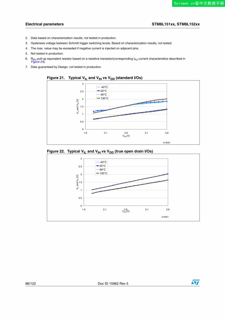
Electrical parameters STM8L151xx, STM8L152xx
86/122 Doc ID 15962 Rev 5
Figure 21. Typical VIL and VIH vs VDD (standard I/Os)
Figure 22. Typical VIL and VIH vs VDD (true open drain I/Os)
2. Data based on characterization results, not tested in production.
3. Hysteresis voltage between Schmitt trigger switching levels. Based on characterization results, not tested.
4. The max. value may be exceeded if negative current is injected on adjacent pins.
5. Not tested in production.
6. RPU pull-up equivalent resistor based on a resistive transistor(corresponding IPU current characteristics described in Figure 24).
7. Data guaranteed by Design, not tested in production.
Soiseek.cn看中文数据手册
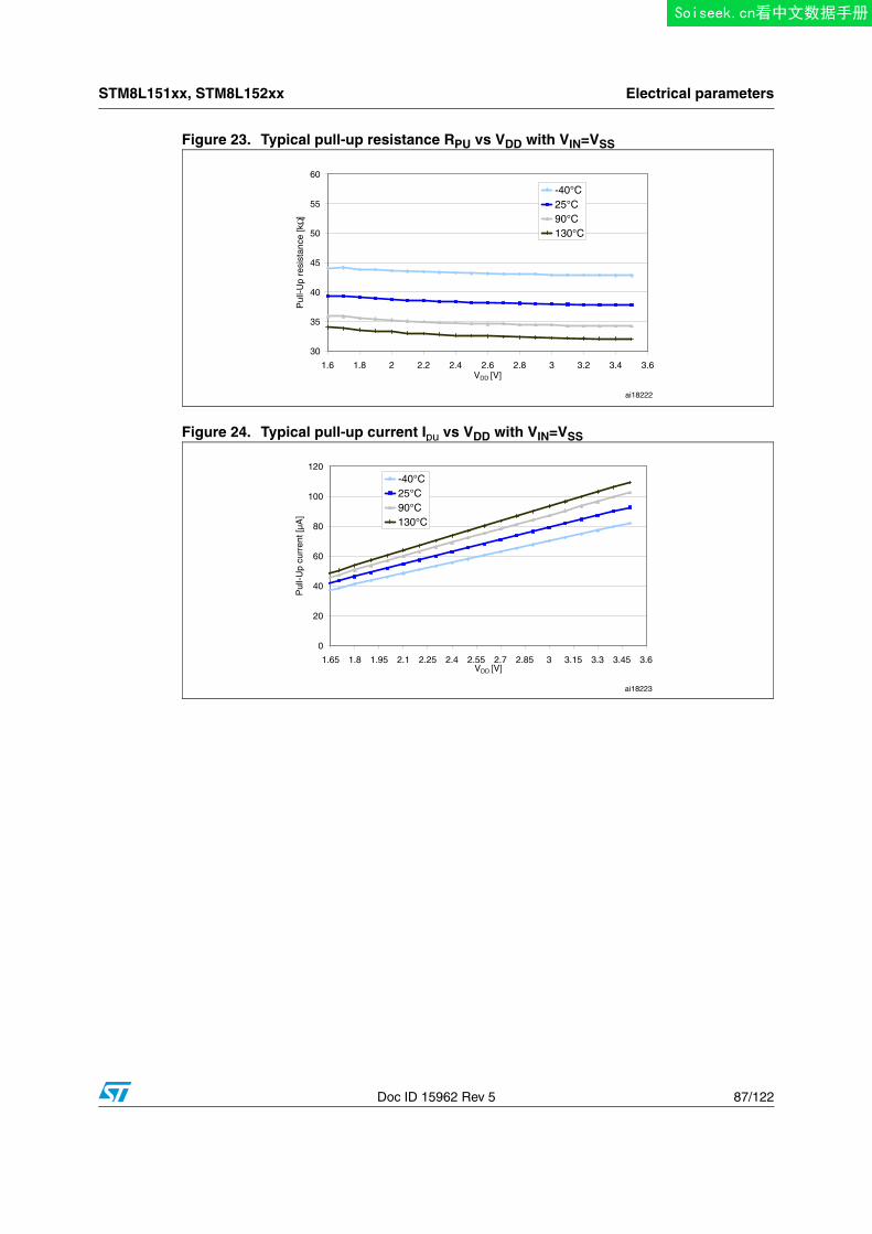
STM8L151xx, STM8L152xx Electrical parameters
Doc ID 15962 Rev 5 87/122
Figure 23. Typical pull-up resistance RPU vs VDD with VIN=VSS
Figure 24. Typical pull-up current Ipu vs VDD with VIN=VSS
Soiseek.cn看中文数据手册
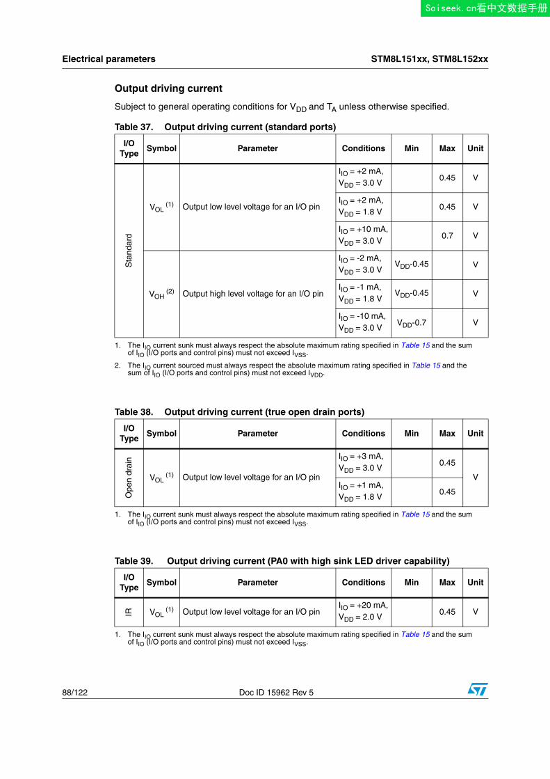
Electrical parameters STM8L151xx, STM8L152xx
88/122 Doc ID 15962 Rev 5
Output driving current
Subject to general operating conditions for VDD and TA unless otherwise specified.
Table 37. Output driving current (standard ports)
I/O Type
Symbol Parameter Conditions Min Max Unit
Sta
ndar
d
VOL (1)
1. The IIO current sunk must always respect the absolute maximum rating specified in Table 15 and the sum of IIO (I/O ports and control pins) must not exceed IVSS.
Output low level voltage for an I/O pin
IIO = +2 mA,VDD = 3.0 V
0.45 V
IIO = +2 mA,VDD = 1.8 V
0.45 V
IIO = +10 mA,VDD = 3.0 V
0.7 V
VOH (2)
2. The IIO current sourced must always respect the absolute maximum rating specified in Table 15 and the sum of IIO (I/O ports and control pins) must not exceed IVDD.
Output high level voltage for an I/O pin
IIO = -2 mA,VDD = 3.0 V
VDD-0.45 V
IIO = -1 mA,VDD = 1.8 V
VDD-0.45 V
IIO = -10 mA,VDD = 3.0 V
VDD-0.7 V
Table 38. Output driving current (true open drain ports)
I/O Type
Symbol Parameter Conditions Min Max Unit
Ope
n dr
ain
VOL (1)
1. The IIO current sunk must always respect the absolute maximum rating specified in Table 15 and the sum of IIO (I/O ports and control pins) must not exceed IVSS.
Output low level voltage for an I/O pin
IIO = +3 mA,VDD = 3.0 V
0.45
VIIO = +1 mA,VDD = 1.8 V
0.45
Table 39. Output driving current (PA0 with high sink LED driver capability)
I/O Type
Symbol Parameter Conditions Min Max Unit
IR VOL (1)
1. The IIO current sunk must always respect the absolute maximum rating specified in Table 15 and the sum of IIO (I/O ports and control pins) must not exceed IVSS.
Output low level voltage for an I/O pinIIO = +20 mA,VDD = 2.0 V
0.45 V
Soiseek.cn看中文数据手册
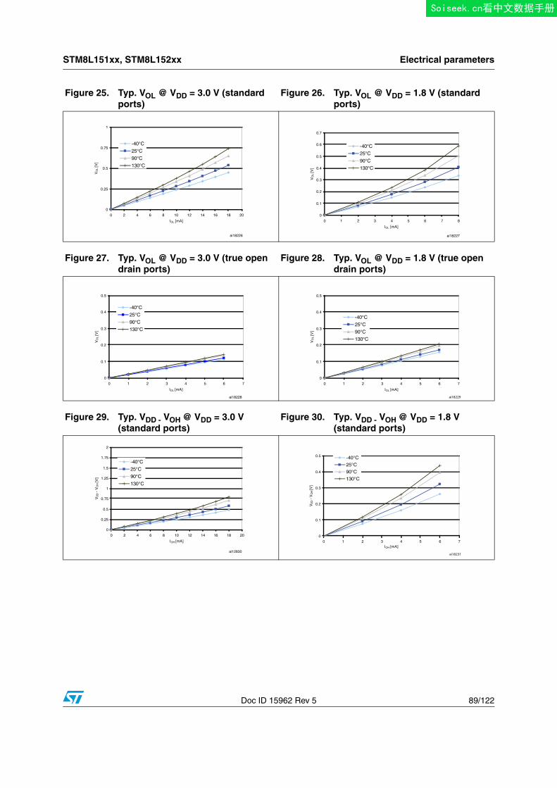
STM8L151xx, STM8L152xx Electrical parameters
Doc ID 15962 Rev 5 89/122
Figure 25. Typ. VOL @ VDD = 3.0 V (standard ports)
Figure 26. Typ. VOL @ VDD = 1.8 V (standard ports)
Figure 27. Typ. VOL @ VDD = 3.0 V (true open drain ports)
Figure 28. Typ. VOL @ VDD = 1.8 V (true open drain ports)
Figure 29. Typ. VDD - VOH @ VDD = 3.0 V (standard ports)
Figure 30. Typ. VDD - VOH @ VDD = 1.8 V (standard ports)
Soiseek.cn看中文数据手册
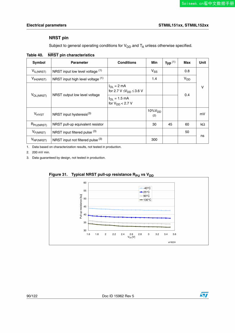
Electrical parameters STM8L151xx, STM8L152xx
90/122 Doc ID 15962 Rev 5
NRST pin
Subject to general operating conditions for VDD and TA unless otherwise specified.
Figure 31. Typical NRST pull-up resistance RPU vs VDD
Table 40. NRST pin characteristics
Symbol Parameter Conditions Min Typ (1) Max Unit
VIL(NRST) NRST input low level voltage (1) VSS 0.8
V
VIH(NRST) NRST input high level voltage (1) 1.4 VDD
VOL(NRST) NRST output low level voltage
IOL = 2 mAfor 2.7 V ≤ VDD ≤ 3.6 V
0.4IOL = 1.5 mAfor VDD < 2.7 V
VHYST NRST input hysteresis(3)10%VDD
(2) mV
RPU(NRST) NRST pull-up equivalent resistor 30 45 60 kΩ
VF(NRST) NRST input filtered pulse (3) 50ns
VNF(NRST) NRST input not filtered pulse (3) 300
1. Data based on characterization results, not tested in production.
2. 200 mV min.
3. Data guaranteed by design, not tested in production.
Soiseek.cn看中文数据手册
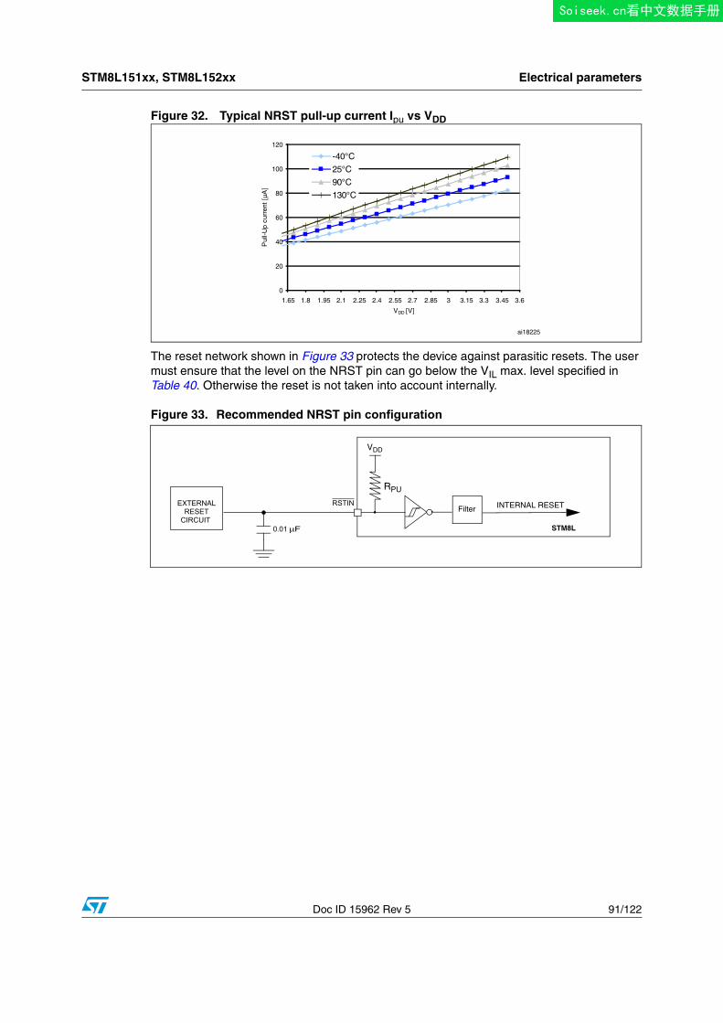
STM8L151xx, STM8L152xx Electrical parameters
Doc ID 15962 Rev 5 91/122
Figure 32. Typical NRST pull-up current Ipu vs VDD
The reset network shown in Figure 33 protects the device against parasitic resets. The user must ensure that the level on the NRST pin can go below the VIL max. level specified in Table 40. Otherwise the reset is not taken into account internally.
Figure 33. Recommended NRST pin configuration
0.01 μF
EXTERNALRESETCIRCUIT
STM8L
Filter
RPU
VDD
INTERNAL RESETRSTIN
Soiseek.cn看中文数据手册
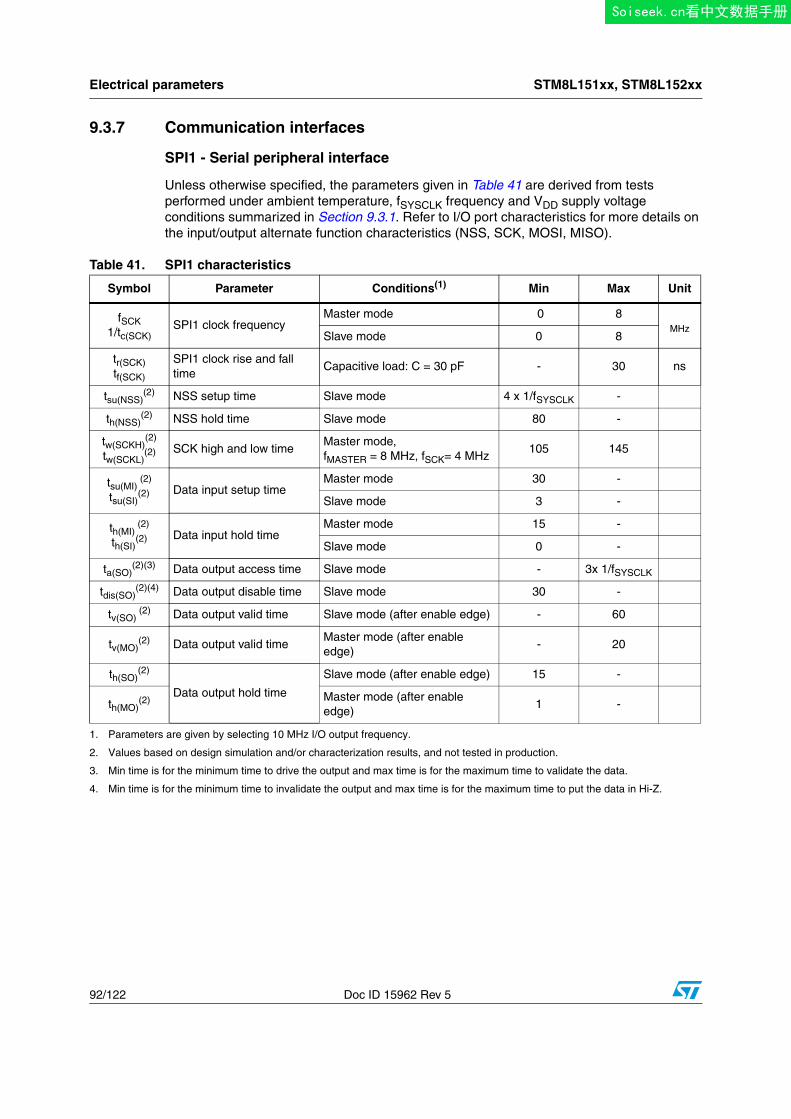
Electrical parameters STM8L151xx, STM8L152xx
92/122 Doc ID 15962 Rev 5
9.3.7 Communication interfaces
SPI1 - Serial peripheral interface
Unless otherwise specified, the parameters given in Table 41 are derived from tests performed under ambient temperature, fSYSCLK frequency and VDD supply voltage conditions summarized in Section 9.3.1. Refer to I/O port characteristics for more details on the input/output alternate function characteristics (NSS, SCK, MOSI, MISO).
Table 41. SPI1 characteristics
Symbol Parameter Conditions(1) Min Max Unit
fSCK1/tc(SCK)
SPI1 clock frequencyMaster mode 0 8
MHzSlave mode 0 8
tr(SCK)tf(SCK)
SPI1 clock rise and fall time
Capacitive load: C = 30 pF - 30 ns
tsu(NSS)(2) NSS setup time Slave mode 4 x 1/fSYSCLK -
th(NSS)(2) NSS hold time Slave mode 80 -
tw(SCKH)(2)
tw(SCKL)(2) SCK high and low time
Master mode, fMASTER = 8 MHz, fSCK= 4 MHz
105 145
tsu(MI) (2)
tsu(SI)(2) Data input setup time
Master mode 30 -
Slave mode 3 -
th(MI) (2)
th(SI)(2) Data input hold time
Master mode 15 -
Slave mode 0 -
ta(SO)(2)(3) Data output access time Slave mode - 3x 1/fSYSCLK
tdis(SO)(2)(4) Data output disable time Slave mode 30 -
tv(SO) (2) Data output valid time Slave mode (after enable edge) - 60
tv(MO)(2) Data output valid time
Master mode (after enable edge)
- 20
th(SO)(2)
Data output hold time
Slave mode (after enable edge) 15 -
th(MO)(2) Master mode (after enable
edge)1 -
1. Parameters are given by selecting 10 MHz I/O output frequency.
2. Values based on design simulation and/or characterization results, and not tested in production.
3. Min time is for the minimum time to drive the output and max time is for the maximum time to validate the data.
4. Min time is for the minimum time to invalidate the output and max time is for the maximum time to put the data in Hi-Z.
Soiseek.cn看中文数据手册
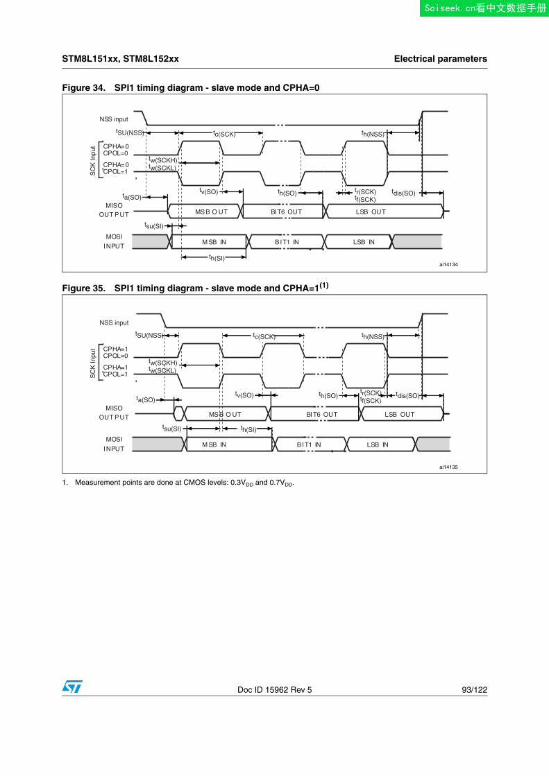
STM8L151xx, STM8L152xx Electrical parameters
Doc ID 15962 Rev 5 93/122
Figure 34. SPI1 timing diagram - slave mode and CPHA=0
Figure 35. SPI1 timing diagram - slave mode and CPHA=1(1)
1. Measurement points are done at CMOS levels: 0.3VDD and 0.7VDD.
ai14134
SC
K In
put CPHA=0
MOSI
INPUT
MISOOUT PUT
CPHA=0
MSB O UT
M SB IN
BIT6 OUT
LSB IN
LSB OUT
CPOL=0
CPOL=1
BIT1 IN
NSS input
tSU(NSS) tc(SCK) th(NSS)
ta(SO)
tw(SCKH)tw(SCKL)
tv(SO) th(SO) tr(SCK)tf(SCK)
tdis(SO)
tsu(SI)
th(SI)
ai14135
SC
K In
put CPHA=1
MOSI
INPUT
MISOOUT PUT
CPHA=1
MSB O UT
M SB IN
BIT6 OUT
LSB IN
LSB OUT
CPOL=0
CPOL=1
BIT1 IN
tSU(NSS) tc(SCK) th(NSS)
ta(SO)
tw(SCKH)tw(SCKL)
tv(SO) th(SO)tr(SCK)tf(SCK)
tdis(SO)
tsu(SI) th(SI)
NSS input
Soiseek.cn看中文数据手册
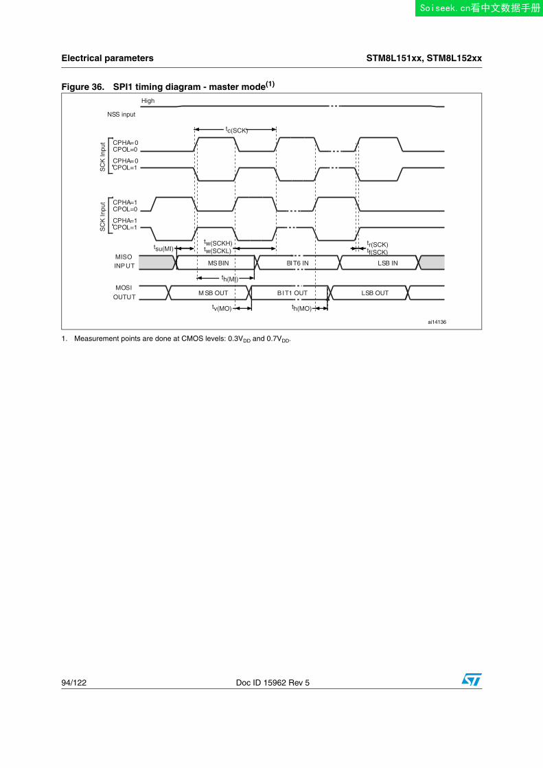
Electrical parameters STM8L151xx, STM8L152xx
94/122 Doc ID 15962 Rev 5
Figure 36. SPI1 timing diagram - master mode(1)
1. Measurement points are done at CMOS levels: 0.3VDD and 0.7VDD.
ai14136
SC
K In
put CPHA=0
MOSI
OUTUT
MISOINPUT
CPHA=0
MSBIN
M SB OUT
BIT6 IN
LSB OUT
LSB IN
CPOL=0
CPOL=1
BIT1 OUT
NSS input
tc(SCK)
tw(SCKH)tw(SCKL)
tr(SCK)tf(SCK)
th(MI)
HighS
CK
Inpu
t CPHA=1
CPHA=1
CPOL=0
CPOL=1
tsu(MI)
tv(MO) th(MO)
Soiseek.cn看中文数据手册
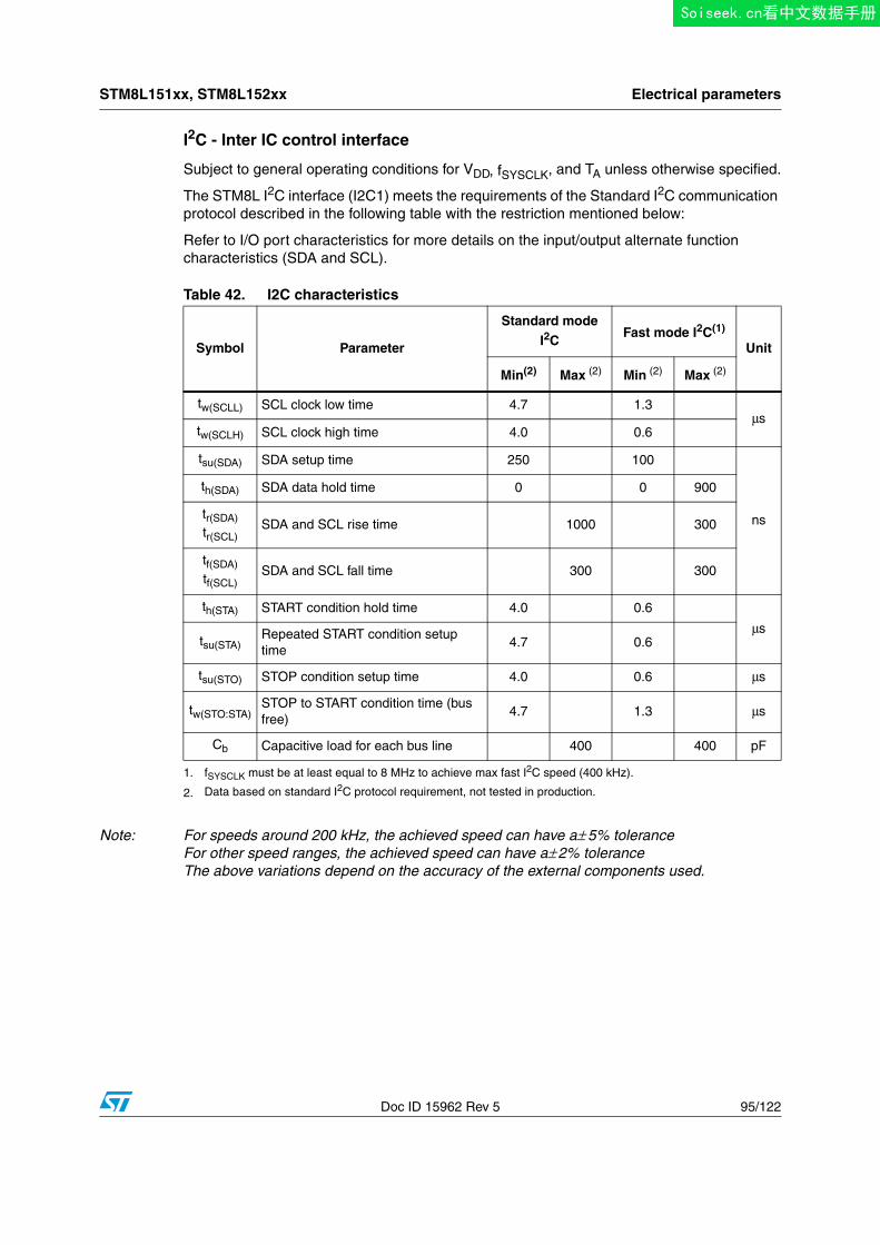
STM8L151xx, STM8L152xx Electrical parameters
Doc ID 15962 Rev 5 95/122
I2C - Inter IC control interface
Subject to general operating conditions for VDD, fSYSCLK, and TA unless otherwise specified.
The STM8L I2C interface (I2C1) meets the requirements of the Standard I2C communication protocol described in the following table with the restriction mentioned below:
Refer to I/O port characteristics for more details on the input/output alternate function characteristics (SDA and SCL).
Note: For speeds around 200 kHz, the achieved speed can have a± 5% toleranceFor other speed ranges, the achieved speed can have a± 2% toleranceThe above variations depend on the accuracy of the external components used.
Table 42. I2C characteristics
Symbol Parameter
Standard mode I2C
Fast mode I2C(1)
1. fSYSCLK must be at least equal to 8 MHz to achieve max fast I2C speed (400 kHz).
Unit
Min(2)
2. Data based on standard I2C protocol requirement, not tested in production.
Max (2) Min (2) Max (2)
tw(SCLL) SCL clock low time 4.7 1.3 μs
tw(SCLH) SCL clock high time 4.0 0.6
tsu(SDA) SDA setup time 250 100
ns
th(SDA) SDA data hold time 0 0 900
tr(SDA)tr(SCL)
SDA and SCL rise time 1000 300
tf(SDA)tf(SCL)
SDA and SCL fall time 300 300
th(STA) START condition hold time 4.0 0.6
μstsu(STA)
Repeated START condition setup time
4.7 0.6
tsu(STO) STOP condition setup time 4.0 0.6 μs
tw(STO:STA)STOP to START condition time (bus free)
4.7 1.3 μs
Cb Capacitive load for each bus line 400 400 pF
Soiseek.cn看中文数据手册
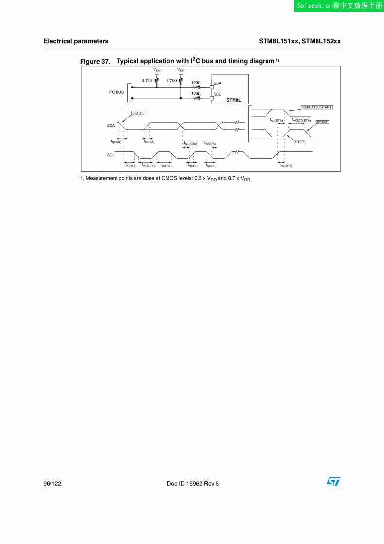
Electrical parameters STM8L151xx, STM8L152xx
96/122 Doc ID 15962 Rev 5
Figure 37. Typical application with I2C bus and timing diagram 1)
1. Measurement points are done at CMOS levels: 0.3 x VDD and 0.7 x VDD
REPEATED START
START
STOP
START
tf(SDA) tr(SDA) tsu(SDA) th(SDA)
tf(SCL)tr(SCL)tw(SCLL)tw(SCLH)th(STA) tsu(STO)
tsu(STA) tw(STO:STA)
SDA
SCL
4.7kΩSDA
STM8LSCL
VDD
100Ω
100Ω
VDD
4.7kΩ
I2C BUS
Soiseek.cn看中文数据手册
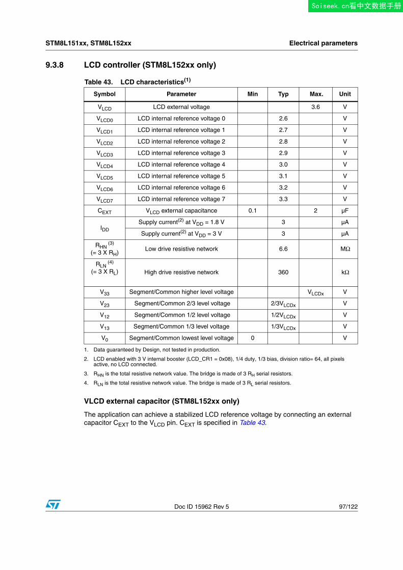
STM8L151xx, STM8L152xx Electrical parameters
Doc ID 15962 Rev 5 97/122
9.3.8 LCD controller (STM8L152xx only)
VLCD external capacitor (STM8L152xx only)
The application can achieve a stabilized LCD reference voltage by connecting an external capacitor CEXT to the VLCD pin. CEXT is specified in Table 43.
Table 43. LCD characteristics(1)
1. Data guaranteed by Design, not tested in production.
Symbol Parameter Min Typ Max. Unit
VLCD LCD external voltage 3.6 V
VLCD0 LCD internal reference voltage 0 2.6 V
VLCD1 LCD internal reference voltage 1 2.7 V
VLCD2 LCD internal reference voltage 2 2.8 V
VLCD3 LCD internal reference voltage 3 2.9 V
VLCD4 LCD internal reference voltage 4 3.0 V
VLCD5 LCD internal reference voltage 5 3.1 V
VLCD6 LCD internal reference voltage 6 3.2 V
VLCD7 LCD internal reference voltage 7 3.3 V
CEXT VLCD external capacitance 0.1 2 µF
IDD
Supply current(2) at VDD = 1.8 V
2. LCD enabled with 3 V internal booster (LCD_CR1 = 0x08), 1/4 duty, 1/3 bias, division ratio= 64, all pixels active, no LCD connected.
3 µA
Supply current(2) at VDD = 3 V 3 µA
RHN (3)
(= 3 X RH)
3. RHN is the total resistive network value. The bridge is made of 3 RH serial resistors.
Low drive resistive network 6.6 MΩ
RLN (4)
(= 3 X RL)
4. RLN is the total resistive network value. The bridge is made of 3 RL serial resistors.
High drive resistive network 360 kΩ
V33 Segment/Common higher level voltage VLCDx V
V23 Segment/Common 2/3 level voltage 2/3VLCDx V
V12 Segment/Common 1/2 level voltage 1/2VLCDx V
V13 Segment/Common 1/3 level voltage 1/3VLCDx V
V0 Segment/Common lowest level voltage 0 V
Soiseek.cn看中文数据手册
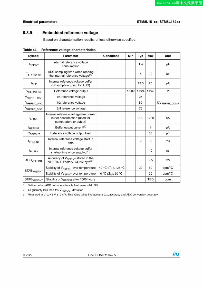
Electrical parameters STM8L151xx, STM8L152xx
98/122 Doc ID 15962 Rev 5
9.3.9 Embedded reference voltage
Based on characterization results, unless otherwise specified.
Table 44. Reference voltage characteristics
Symbol Parameter Conditions Min Typ Max. Unit
IREFINTInternal reference voltage
consumption1.4 µA
TS_VREFINTADC sampling time when reading the internal reference voltage(1) 5 10 µs
IBUFInternal reference voltage buffer
consumption (used for ADC)13.5 25 µA
VREFINT out Reference voltage output 1.202 1.224 1.242 V
VREFINT_DIV1 1/4 reference voltage 25
%VREFINT_COMPVREFNT_DIV2 1/2 reference voltage 50
VREFNT_DIV3 3/4 reference voltage 75
ILPBUF
Internal reference voltage low power buffer consumption (used for
comparators or output)730 1200 nA
IREFOUT Buffer output current(2) 1 µA
CREFOUT Reference voltage output load 50 pF
tVREFINTInternal reference voltage startup
time2 3 ms
tBUFENInternal reference voltage buffer
startup time once enabled (1) 10 µs
ACCVREFINTAccuracy of VREFINT stored in the VREFINT_Factory_CONV byte(3) ± 5 mV
STABVREFINT
Stability of VREFINT over temperature -40 °C ≤ TA ≤ 125 °C 20 50 ppm/°C
Stability of VREFINT over temperature 0 °C ≤ TA ≤ 50 °C 20 ppm/°C
STABVREFINT Stability of VREFINT after 1000 hours TBD ppm
1. Defined when ADC output reaches its final value ±1/2LSB
2. To guaranty less than 1% VREFOUT deviation
3. Measured at VDD = 3 V ±10 mV. This value takes into account VDD accuracy and ADC conversion accuracy.
Soiseek.cn看中文数据手册
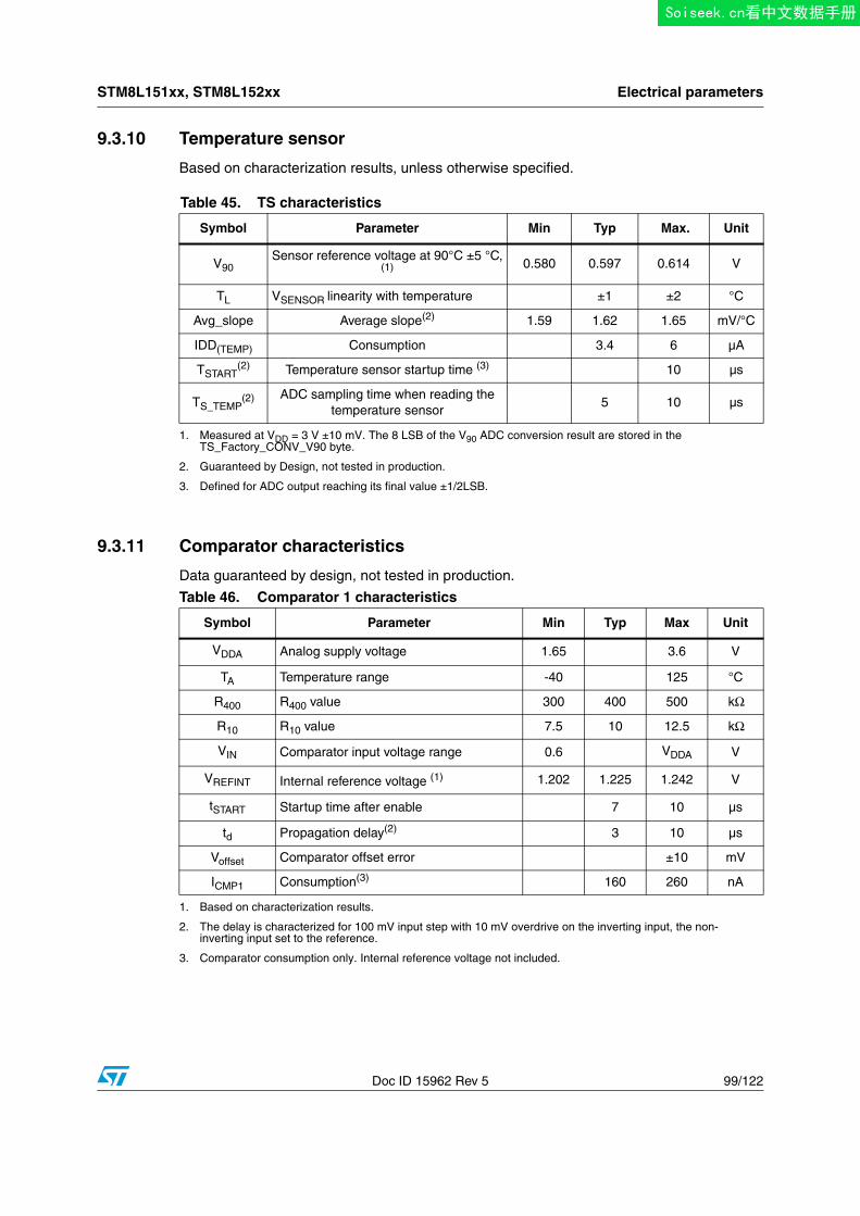
STM8L151xx, STM8L152xx Electrical parameters
Doc ID 15962 Rev 5 99/122
9.3.10 Temperature sensor
Based on characterization results, unless otherwise specified.
9.3.11 Comparator characteristics
Data guaranteed by design, not tested in production.
Table 45. TS characteristics
Symbol Parameter Min Typ Max. Unit
V90Sensor reference voltage at 90°C ±5 °C,
(1)
1. Measured at VDD = 3 V ±10 mV. The 8 LSB of the V90 ADC conversion result are stored in the TS_Factory_CONV_V90 byte.
0.580 0.597 0.614 V
TL VSENSOR linearity with temperature ±1 ±2 °C
Avg_slope Average slope(2) 1.59 1.62 1.65 mV/°C
IDD(TEMP) Consumption 3.4 6 µA
TSTART(2)
2. Guaranteed by Design, not tested in production.
Temperature sensor startup time (3)
3. Defined for ADC output reaching its final value ±1/2LSB.
10 µs
TS_TEMP(2) ADC sampling time when reading the
temperature sensor5 10 µs
Table 46. Comparator 1 characteristics
Symbol Parameter Min Typ Max Unit
VDDA Analog supply voltage 1.65 3.6 V
TA Temperature range -40 125 °C
R400 R400 value 300 400 500 kΩ
R10 R10 value 7.5 10 12.5 kΩ
VIN Comparator input voltage range 0.6 VDDA V
VREFINT Internal reference voltage (1)
1. Based on characterization results.
1.202 1.225 1.242 V
tSTART Startup time after enable 7 10 µs
td Propagation delay(2)
2. The delay is characterized for 100 mV input step with 10 mV overdrive on the inverting input, the non-inverting input set to the reference.
3 10 µs
Voffset Comparator offset error ±10 mV
ICMP1 Consumption(3)
3. Comparator consumption only. Internal reference voltage not included.
160 260 nA
Soiseek.cn看中文数据手册
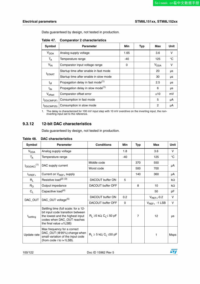
Electrical parameters STM8L151xx, STM8L152xx
100/122 Doc ID 15962 Rev 5
Data guaranteed by design, not tested in production.
9.3.12 12-bit DAC characteristics
Data guaranteed by design, not tested in production.
Table 47. Comparator 2 characteristics
Symbol Parameter Min Typ Max Unit
VDDA Analog supply voltage 1.65 3.6 V
TA Temperature range -40 125 °C
VIN Comparator input voltage range 0 VDDA V
tSTARTStartup time after enable in fast mode 20 µs
Startup time after enable in slow mode 30 µs
tdf Propagation delay in fast mode(1)
1. The delay is characterized for 100 mV input step with 10 mV overdrive on the inverting input, the non-inverting input set to the reference.
2.5 µs
tds Propagation delay in slow mode(1) 6 µs
Voffset Comparator offset error ±10 mV
IDD(CMP2F) Consumption in fast mode 5 µA
IDD(CMP2S) Consumption in slow mode 2 µA
Table 48. DAC characteristics
Symbol Parameter Conditions Min Typ Max Unit
VDDA Analog supply voltage 1.8 3.6 V
TA Temperature range -40 125 °C
IDD(DAC)(1) DAC supply current
Middle code 370 550µA
Worst code 500 700
IVREF+ Current on VREF+ supply 140 360 µA
RL Resistive load(2) (3) DACOUT buffer ON 5 kΩ
RO Output impedance DACOUT buffer OFF 8 10 kΩ
CL Capacitive load(4) 50 pF
DAC_OUT DAC_OUT voltage(5)DACOUT buffer ON 0.2 VREF+-0.2 V
DACOUT buffer OFF 0 VREF+ -1 LSB V
tsettling
Settling time (full scale: for a 12-bit input code transition between the lowest and the highest input codes when DAC_OUT reaches the final value ±1LSB)
RL ≥5 kΩ, CL≤ 50 pF 7 12 µs
Update rate
Max frequency for a correct DAC_OUT (@95%) change when small variation of the input code (from code i to i+1LSB).
RL ≥ 5 kΩ, CL ≤ 50 pF 1 Msps
Soiseek.cn看中文数据手册
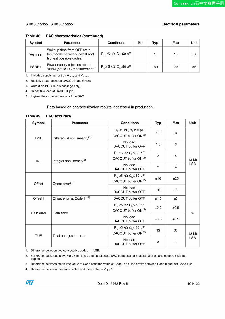
STM8L151xx, STM8L152xx Electrical parameters
Doc ID 15962 Rev 5 101/122
Data based on characterization results, not tested in production.
tWAKEUP
Wakeup time from OFF state. Input code between lowest and highest possible codes.
RL ≥5 kΩ, CL≤ 50 pF 9 15 µs
PSRR+Power supply rejection ratio (to VDDA) (static DC measurement)
RL≥ 5 kΩ, CL≤ 50 pF -60 -35 dB
1. Includes supply current on VDDA and VREF+
2. Resistive load between DACOUT and GNDA
3. Output on PF0 (48-pin package only)
4. Capacitive load at DACOUT pin
5. It gives the output excursion of the DAC
Table 48. DAC characteristics (continued)
Symbol Parameter Conditions Min Typ Max Unit
Table 49. DAC accuracy
Symbol Parameter Conditions Typ Max Unit
DNL Differential non linearity(1)
RL ≥5 kΩ, CL≤50 pF
DACOUT buffer ON(2) 1.5 3
12-bit LSB
No loadDACOUT buffer OFF
1.5 3
INL Integral non linearity(3)
RL ≥5 kΩ, CL≤ 50 pF
DACOUT buffer ON(2) 2 4
No loadDACOUT buffer OFF
2 4
Offset Offset error(4)
RL ≥5 kΩ, CL≤ 50 pF
DACOUT buffer ON(2) ±10 ±25
No loadDACOUT buffer OFF
±5 ±8
Offset1 Offset error at Code 1 (5) DACOUT buffer OFF ±1.5 ±5
Gain error Gain error
RL ≥5 kΩ, CL≤ 50 pF
DACOUT buffer ON(2) ±0.2 ±0.5
%No load
DACOUT buffer OFF±0.3 ±0.5
TUE Total unadjusted error
RL ≥5 kΩ, CL≤ 50 pF
DACOUT buffer ON(2) 12 3012-bit LSBNo load
DACOUT buffer OFF8 12
1. Difference between two consecutive codes - 1 LSB.
2. For 48-pin packages only. For 28-pin and 32-pin packages, DAC output buffer must be kept off and no load must be applied.
3. Difference between measured value at Code i and the value at Code i on a line drawn between Code 0 and last Code 1023.
4. Difference between measured value and ideal value = VREF/2.
Soiseek.cn看中文数据手册
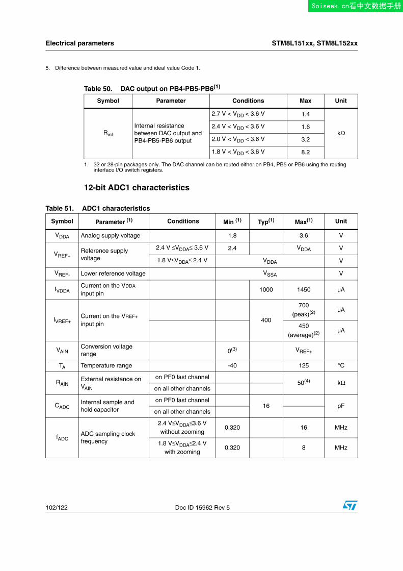
Electrical parameters STM8L151xx, STM8L152xx
102/122 Doc ID 15962 Rev 5
12-bit ADC1 characteristics
5. Difference between measured value and ideal value Code 1.
Table 50. DAC output on PB4-PB5-PB6(1)
1. 32 or 28-pin packages only. The DAC channel can be routed either on PB4, PB5 or PB6 using the routing interface I/O switch registers.
Symbol Parameter Conditions Max Unit
Rint
Internal resistance between DAC output and PB4-PB5-PB6 output
2.7 V < VDD < 3.6 V 1.4
kΩ2.4 V < VDD < 3.6 V 1.6
2.0 V < VDD < 3.6 V 3.2
1.8 V < VDD < 3.6 V 8.2
Table 51. ADC1 characteristics
Symbol Parameter (1) Conditions Min (1) Typ(1) Max(1) Unit
VDDA Analog supply voltage 1.8 3.6 V
VREF+Reference supply voltage
2.4 V ≤ VDDA≤ 3.6 V 2.4 VDDA V
1.8 V≤ VDDA≤ 2.4 V VDDA V
VREF- Lower reference voltage VSSA V
IVDDACurrent on the VDDA
input pin1000 1450 µA
IVREF+Current on the VREF+
input pin400
700
(peak)(2) µA
450
(average)(2) µA
VAINConversion voltage range 0(3) VREF+
TA Temperature range -40 125 °C
RAINExternal resistance on VAIN
on PF0 fast channel50(4) kΩ
on all other channels
CADCInternal sample and hold capacitor
on PF0 fast channel16 pF
on all other channels
fADCADC sampling clock frequency
2.4 V≤ VDDA≤ 3.6 Vwithout zooming
0.320 16 MHz
1.8 V≤ VDDA≤ 2.4 Vwith zooming
0.320 8 MHz
Soiseek.cn看中文数据手册
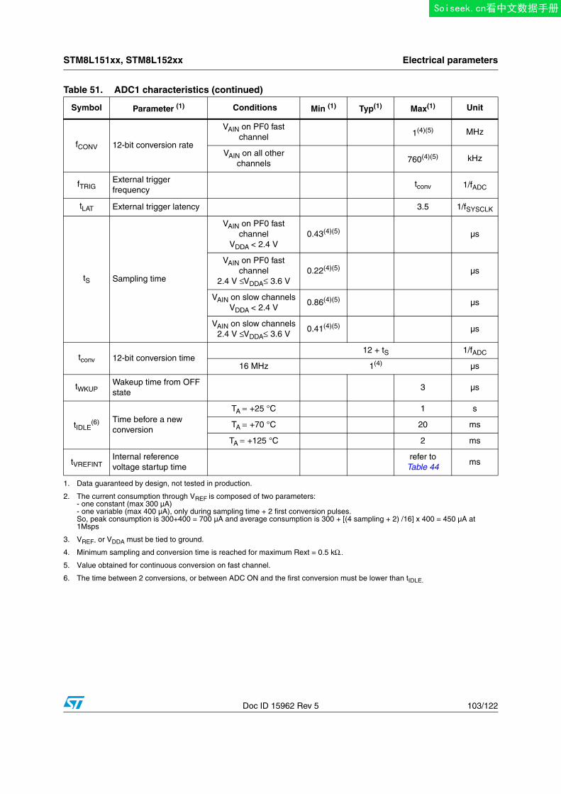
STM8L151xx, STM8L152xx Electrical parameters
Doc ID 15962 Rev 5 103/122
fCONV 12-bit conversion rate
VAIN on PF0 fast channel 1(4)(5) MHz
VAIN on all other channels 760(4)(5) kHz
fTRIGExternal trigger frequency
tconv 1/fADC
tLAT External trigger latency 3.5 1/fSYSCLK
tS Sampling time
VAIN on PF0 fast channel
VDDA < 2.4 V0.43(4)(5) µs
VAIN on PF0 fast channel
2.4 V ≤ VDDA≤ 3.6 V0.22(4)(5) µs
VAIN on slow channelsVDDA < 2.4 V
0.86(4)(5) µs
VAIN on slow channels2.4 V ≤ VDDA≤ 3.6 V
0.41(4)(5) µs
tconv 12-bit conversion time12 + tS 1/fADC
16 MHz 1(4) µs
tWKUPWakeup time from OFF state
3 µs
tIDLE(6) Time before a new
conversion
TA = +25 °C 1 s
TA = +70 °C 20 ms
TA = +125 °C 2 ms
tVREFINTInternal reference voltage startup time
refer to Table 44
ms
1. Data guaranteed by design, not tested in production.
2. The current consumption through VREF is composed of two parameters:- one constant (max 300 µA)- one variable (max 400 µA), only during sampling time + 2 first conversion pulses.So, peak consumption is 300+400 = 700 µA and average consumption is 300 + [(4 sampling + 2) /16] x 400 = 450 µA at 1Msps
3. VREF- or VDDA must be tied to ground.
4. Minimum sampling and conversion time is reached for maximum Rext = 0.5 kΩ..
5. Value obtained for continuous conversion on fast channel.
6. The time between 2 conversions, or between ADC ON and the first conversion must be lower than tIDLE.
Table 51. ADC1 characteristics (continued)
Symbol Parameter (1) Conditions Min (1) Typ(1) Max(1) Unit
Soiseek.cn看中文数据手册
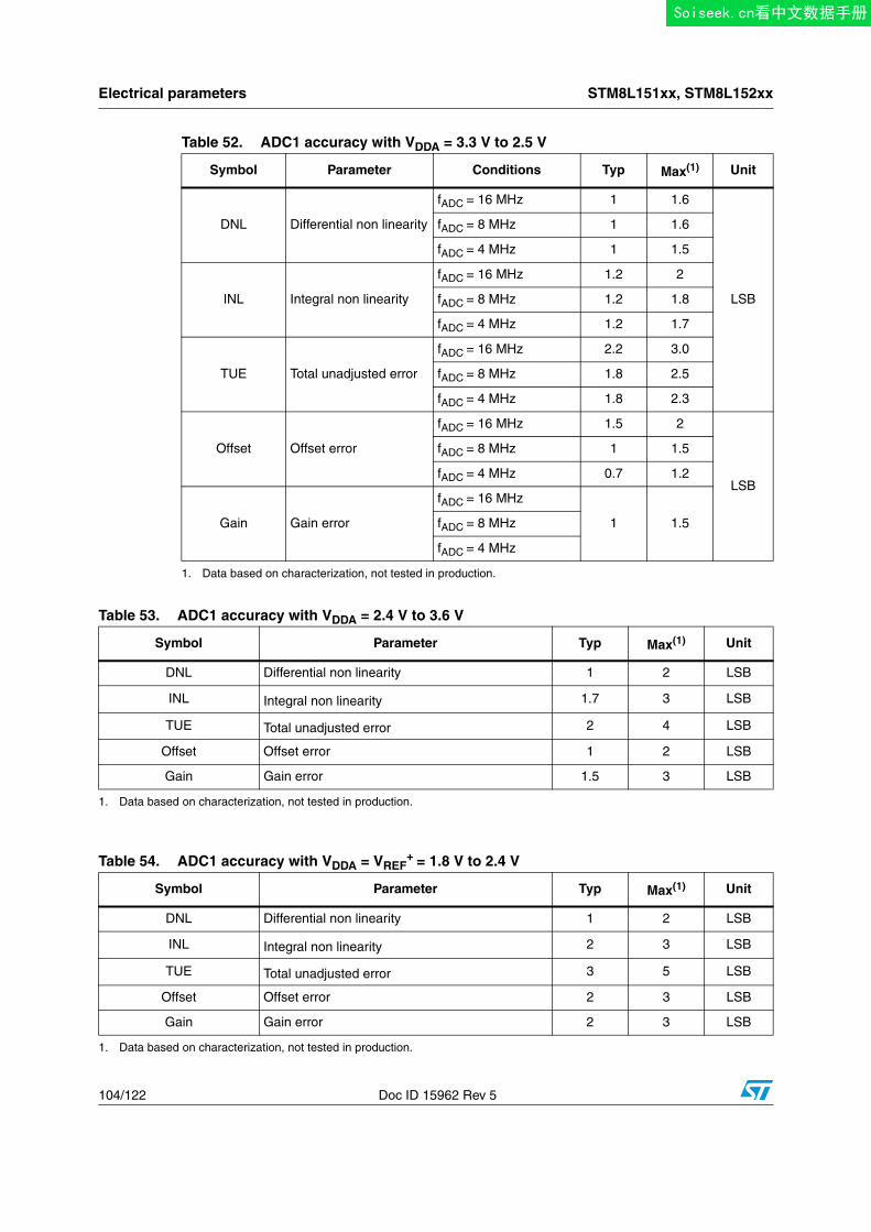
Electrical parameters STM8L151xx, STM8L152xx
104/122 Doc ID 15962 Rev 5
Table 52. ADC1 accuracy with VDDA = 3.3 V to 2.5 V
Symbol Parameter Conditions Typ Max(1)
1. Data based on characterization, not tested in production.
Unit
DNL Differential non linearity
fADC = 16 MHz 1 1.6
LSB
fADC = 8 MHz 1 1.6
fADC = 4 MHz 1 1.5
INL Integral non linearity
fADC = 16 MHz 1.2 2
fADC = 8 MHz 1.2 1.8
fADC = 4 MHz 1.2 1.7
TUE Total unadjusted error
fADC = 16 MHz 2.2 3.0
fADC = 8 MHz 1.8 2.5
fADC = 4 MHz 1.8 2.3
Offset Offset error
fADC = 16 MHz 1.5 2
LSB
fADC = 8 MHz 1 1.5
fADC = 4 MHz 0.7 1.2
Gain Gain error
fADC = 16 MHz
1 1.5fADC = 8 MHz
fADC = 4 MHz
Table 53. ADC1 accuracy with VDDA = 2.4 V to 3.6 V
Symbol Parameter Typ Max(1) Unit
DNL Differential non linearity 1 2 LSB
INL Integral non linearity 1.7 3 LSB
TUE Total unadjusted error 2 4 LSB
Offset Offset error 1 2 LSB
Gain Gain error 1.5 3 LSB
1. Data based on characterization, not tested in production.
Table 54. ADC1 accuracy with VDDA = VREF+ = 1.8 V to 2.4 V
Symbol Parameter Typ Max(1) Unit
DNL Differential non linearity 1 2 LSB
INL Integral non linearity 2 3 LSB
TUE Total unadjusted error 3 5 LSB
Offset Offset error 2 3 LSB
Gain Gain error 2 3 LSB
1. Data based on characterization, not tested in production.
Soiseek.cn看中文数据手册
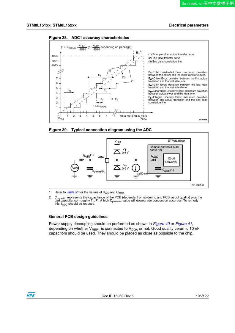
STM8L151xx, STM8L152xx Electrical parameters
Doc ID 15962 Rev 5 105/122
Figure 38. ADC1 accuracy characteristics
Figure 39. Typical connection diagram using the ADC
1. Refer to Table 51 for the values of RAIN and CADC.
2. Cparasitic represents the capacitance of the PCB (dependent on soldering and PCB layout quality) plus the pad capacitance (roughly 7 pF). A high Cparasitic value will downgrade conversion accuracy. To remedy this, fADC should be reduced.
General PCB design guidelines
Power supply decoupling should be performed as shown in Figure 40 or Figure 41, depending on whether VREF+ is connected to VDDA or not. Good quality ceramic 10 nF capacitors should be used. They should be placed as close as possible to the chip.
EO
EG
1 LSBIDEAL
(1) Example of an actual transfer curve(2) The ideal transfer curve(3) End point correlation line
ET=Total Unadjusted Error: maximum deviationbetween the actual and the ideal transfer curves.EO=Offset Error: deviation between the first actualtransition and the first ideal one.EG=Gain Error: deviation between the last idealtransition and the last actual one.ED=Differential Linearity Error: maximum deviationbetween actual steps and the ideal one.EL=Integral Linearity Error: maximum deviationbetween any actual transition and the end pointcorrelation line.
4095
4094
4093
5
4
3
2
1
0
7
6
1 2 3 4 5 6 7 4093 4094 4095 4096
(1)
(2)
ET
ED
EL
(3)
VDDAVSSA ai14395b
VREF+
4096(or depending on package)]
VDDA
4096[1LSBIDEAL =
Soiseek.cn看中文数据手册
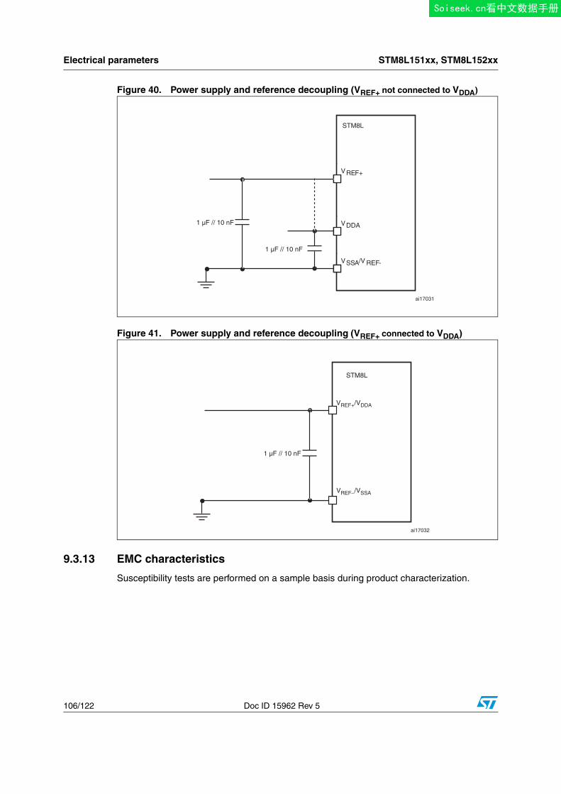
Electrical parameters STM8L151xx, STM8L152xx
106/122 Doc ID 15962 Rev 5
Figure 40. Power supply and reference decoupling (VREF+ not connected to VDDA)
Figure 41. Power supply and reference decoupling (VREF+ connected to VDDA)
9.3.13 EMC characteristics
Susceptibility tests are performed on a sample basis during product characterization.
VREF+
STM8L
VDDA
VSSA/V REF-
1 µF // 10 nF
1 µF // 10 nF
ai17031
VREF+/VDDA
STM8L
1 µF // 10 nF
VREF–/VSSA
ai17032
Soiseek.cn看中文数据手册
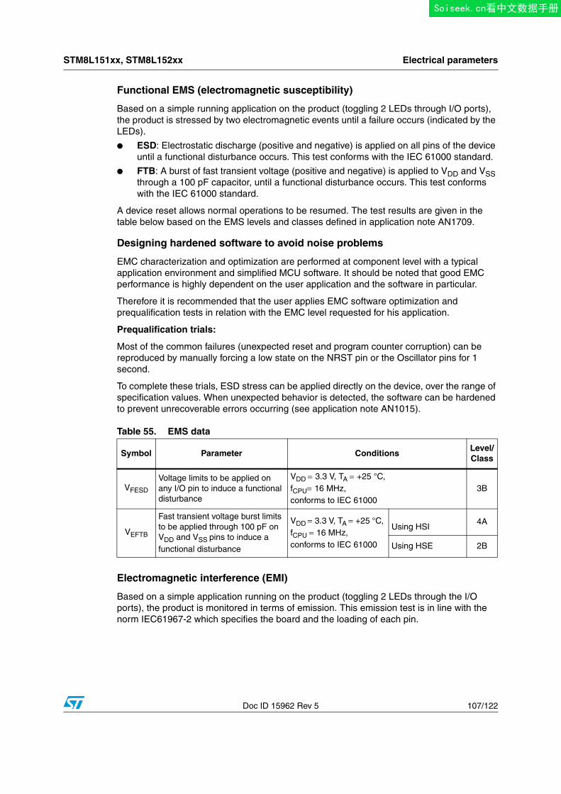
STM8L151xx, STM8L152xx Electrical parameters
Doc ID 15962 Rev 5 107/122
Functional EMS (electromagnetic susceptibility)
Based on a simple running application on the product (toggling 2 LEDs through I/O ports), the product is stressed by two electromagnetic events until a failure occurs (indicated by the LEDs).
● ESD: Electrostatic discharge (positive and negative) is applied on all pins of the device until a functional disturbance occurs. This test conforms with the IEC 61000 standard.
● FTB: A burst of fast transient voltage (positive and negative) is applied to VDD and VSS through a 100 pF capacitor, until a functional disturbance occurs. This test conforms with the IEC 61000 standard.
A device reset allows normal operations to be resumed. The test results are given in the table below based on the EMS levels and classes defined in application note AN1709.
Designing hardened software to avoid noise problems
EMC characterization and optimization are performed at component level with a typical application environment and simplified MCU software. It should be noted that good EMC performance is highly dependent on the user application and the software in particular.
Therefore it is recommended that the user applies EMC software optimization and prequalification tests in relation with the EMC level requested for his application.
Prequalification trials:
Most of the common failures (unexpected reset and program counter corruption) can be reproduced by manually forcing a low state on the NRST pin or the Oscillator pins for 1 second.
To complete these trials, ESD stress can be applied directly on the device, over the range of specification values. When unexpected behavior is detected, the software can be hardened to prevent unrecoverable errors occurring (see application note AN1015).
Electromagnetic interference (EMI)
Based on a simple application running on the product (toggling 2 LEDs through the I/O ports), the product is monitored in terms of emission. This emission test is in line with the norm IEC61967-2 which specifies the board and the loading of each pin.
Table 55. EMS data
Symbol Parameter ConditionsLevel/Class
VFESD
Voltage limits to be applied on any I/O pin to induce a functional disturbance
VDD = 3.3 V, TA = +25 °C, fCPU= 16 MHz,conforms to IEC 61000
3B
VEFTB
Fast transient voltage burst limits to be applied through 100 pF on VDD and VSS pins to induce a functional disturbance
VDD = 3.3 V, TA = +25 °C, fCPU = 16 MHz,conforms to IEC 61000
Using HSI4A
Using HSE 2B
Soiseek.cn看中文数据手册
Electrical parameters STM8L151xx, STM8L152xx
108/122 Doc ID 15962 Rev 5
Absolute maximum ratings (electrical sensitivity)
Based on two different tests (ESD and LU) using specific measurement methods, the product is stressed in order to determine its performance in terms of electrical sensitivity. For more details, refer to the application note AN1181.
Electrostatic discharge (ESD)
Electrostatic discharges (a positive then a negative pulse separated by 1 second) are applied to the pins of each sample according to each pin combination. The sample size depends on the number of supply pins in the device (3 parts*(n+1) supply pin). Two models can be simulated: human body model and charge device model. This test conforms to the JESD22-A114A/A115A standard.
Static latch-up
● LU: 3 complementary static tests are required on 10 parts to assess the latch-up performance. A supply overvoltage (applied to each power supply pin) and a current injection (applied to each input, output and configurable I/O pin) are performed on each sample. This test conforms to the EIA/JESD 78 IC latch-up standard. For more details, refer to the application note AN1181.
Table 56. EMI data (1)
1. Not tested in production.
Symbol Parameter ConditionsMonitored
frequency band
Max vs. Unit
16 MHz
SEMI Peak level
VDD = 3.6 V,TA = +25 °C,LQFP32conforming to IEC61967-2
0.1 MHz to 30 MHz -3
dBμV30 MHz to 130 MHz -9
130 MHz to 1 GHz 4
SAE EMI Level 2 -
Table 57. ESD absolute maximum ratings
Symbol Ratings ConditionsMaximum value (1)
1. Data based on characterization results, not tested in production.
Unit
VESD(HBM)Electrostatic discharge voltage(human body model)
TA = +25 °C
2000
V
VESD(CDM)Electrostatic discharge voltage(charge device model)
500
Table 58. Electrical sensitivities
Symbol Parameter Class
LU Static latch-up class II
Soiseek.cn看中文数据手册
STM8L151xx, STM8L152xx Electrical parameters
Doc ID 15962 Rev 5 109/122
9.4 Thermal characteristicsThe maximum chip junction temperature (TJmax) must never exceed the values given in Table 17: General operating conditions on page 63.
The maximum chip-junction temperature, TJmax, in degree Celsius, may be calculated using the following equation:
TJmax = TAmax + (PDmax x ΘJA)
Where:
● TAmax is the maximum ambient temperature in ° C
● ΘJA is the package junction-to-ambient thermal resistance in ° C/W
● PDmax is the sum of PINTmax and PI/Omax (PDmax = PINTmax + PI/Omax)
● PINTmax is the product of IDD and VDD, expressed in Watts. This is the maximum chip internal power.
● PI/Omax represents the maximum power dissipation on output pinsWhere:PI/Omax = Σ (VOL*IOL) + Σ((VDD-VOH)*I OH), taking into account the actual VOL/IOL and VOH/IOH of the I/Os at low and high level in the application.
Table 59. Thermal characteristics(1)
1. Thermal resistances are based on JEDEC JESD51-2 with 4-layer PCB in a natural convection environment.
Symbol Parameter Value Unit
ΘJAThermal resistance junction-ambientUFQFPN28 - 4 x 4 mm
118 °C/W
ΘJAThermal resistance junction-ambientWLCSP28
70 °C/W
ΘJAThermal resistance junction-ambientLQFP 32 - 7 x 7 mm
59 °C/W
ΘJAThermal resistance junction-ambientUFQFPN 32 - 5 x 5 mm
38 °C/W
ΘJAThermal resistance junction-ambientLQFP 48- 7 x 7 mm
65 °C/W
ΘJAThermal resistance junction-ambientUFQFPN 48- 7 x 7mm
32 °C/W
Soiseek.cn看中文数据手册
Package characteristics STM8L151xx, STM8L152xx
110/122 Doc ID 15962 Rev 5
10 Package characteristics
10.1 ECOPACKIn order to meet environmental requirements, ST offers these devices in different grades of ECOPACK® packages, depending on their level of environmental compliance. ECOPACK® specifications, grade definitions and product status are available at: www.st.com. ECOPACK® is an ST trademark.
Soiseek.cn看中文数据手册
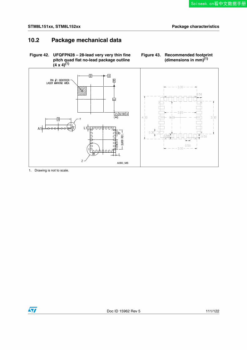
STM8L151xx, STM8L152xx Package characteristics
Doc ID 15962 Rev 5 111/122
10.2 Package mechanical data
Figure 42. UFQFPN28 – 28-lead very very thin fine pitch quad flat no-lead package outline (4 x 4)(1)
Figure 43. Recommended footprint (dimensions in mm)(1)
1. Drawing is not to scale.
Soiseek.cn看中文数据手册
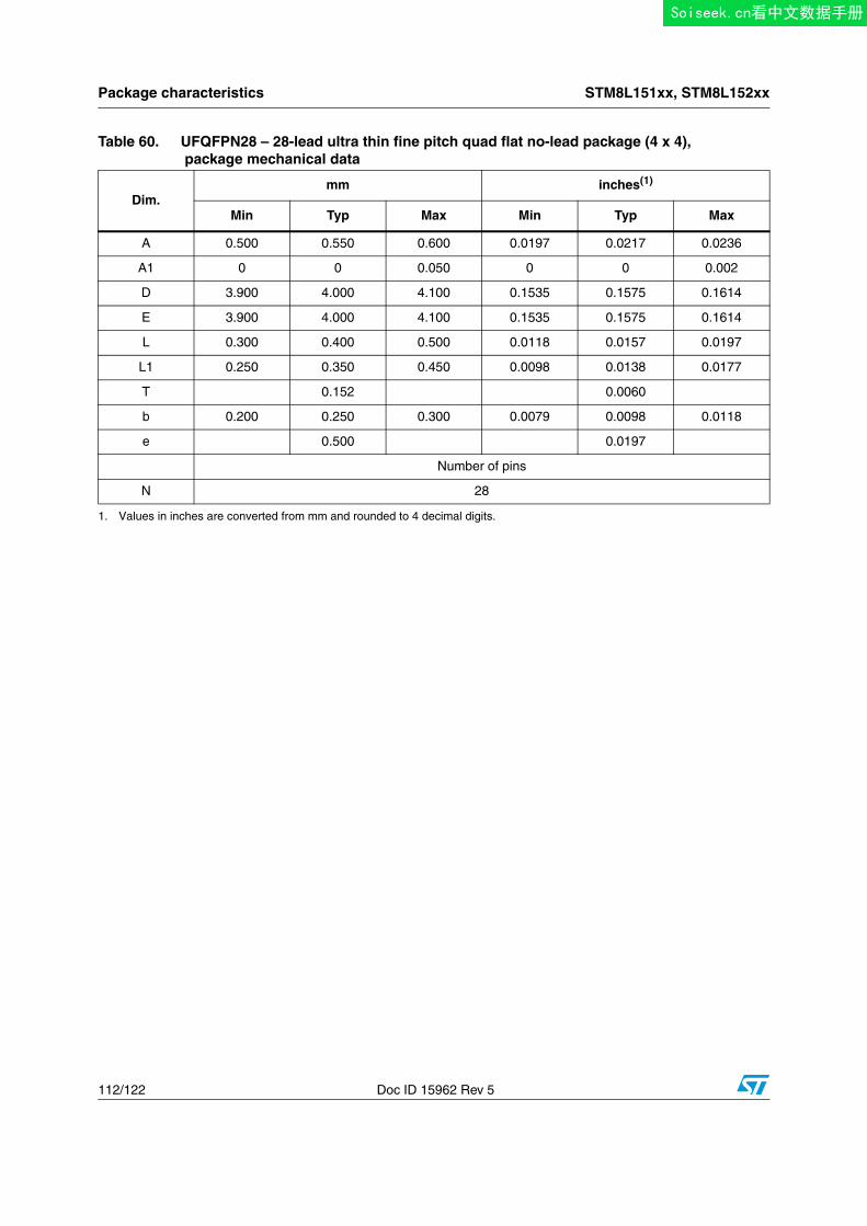
Package characteristics STM8L151xx, STM8L152xx
112/122 Doc ID 15962 Rev 5
Table 60. UFQFPN28 – 28-lead ultra thin fine pitch quad flat no-lead package (4 x 4), package mechanical data
Dim.mm inches(1)
Min Typ Max Min Typ Max
A 0.500 0.550 0.600 0.0197 0.0217 0.0236
A1 0 0 0.050 0 0 0.002
D 3.900 4.000 4.100 0.1535 0.1575 0.1614
E 3.900 4.000 4.100 0.1535 0.1575 0.1614
L 0.300 0.400 0.500 0.0118 0.0157 0.0197
L1 0.250 0.350 0.450 0.0098 0.0138 0.0177
T 0.152 0.0060
b 0.200 0.250 0.300 0.0079 0.0098 0.0118
e 0.500 0.0197
Number of pins
N 28
1. Values in inches are converted from mm and rounded to 4 decimal digits.
Soiseek.cn看中文数据手册
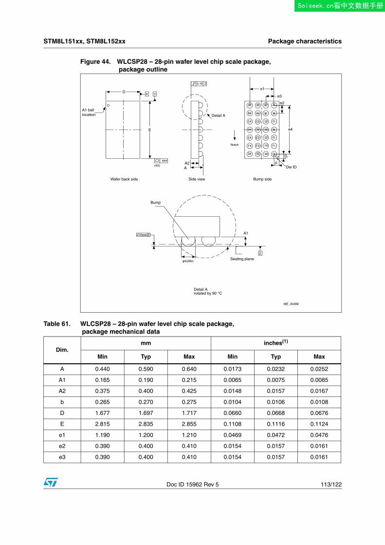
STM8L151xx, STM8L152xx Package characteristics
Doc ID 15962 Rev 5 113/122
Figure 44. WLCSP28 – 28-pin wafer level chip scale package, package outline
Table 61. WLCSP28 – 28-pin wafer level chip scale package, package mechanical data
Dim.mm inches(1)
Min Typ Max Min Typ Max
A 0.440 0.590 0.640 0.0173 0.0232 0.0252
A1 0.165 0.190 0.215 0.0065 0.0075 0.0085
A2 0.375 0.400 0.425 0.0148 0.0157 0.0167
b 0.265 0.270 0.275 0.0104 0.0106 0.0108
D 1.677 1.697 1.717 0.0660 0.0668 0.0676
E 2.815 2.835 2.855 0.1108 0.1116 0.1124
e1 1.190 1.200 1.210 0.0469 0.0472 0.0476
e2 0.390 0.400 0.410 0.0154 0.0157 0.0161
e3 0.390 0.400 0.410 0.0154 0.0157 0.0161
Soiseek.cn看中文数据手册
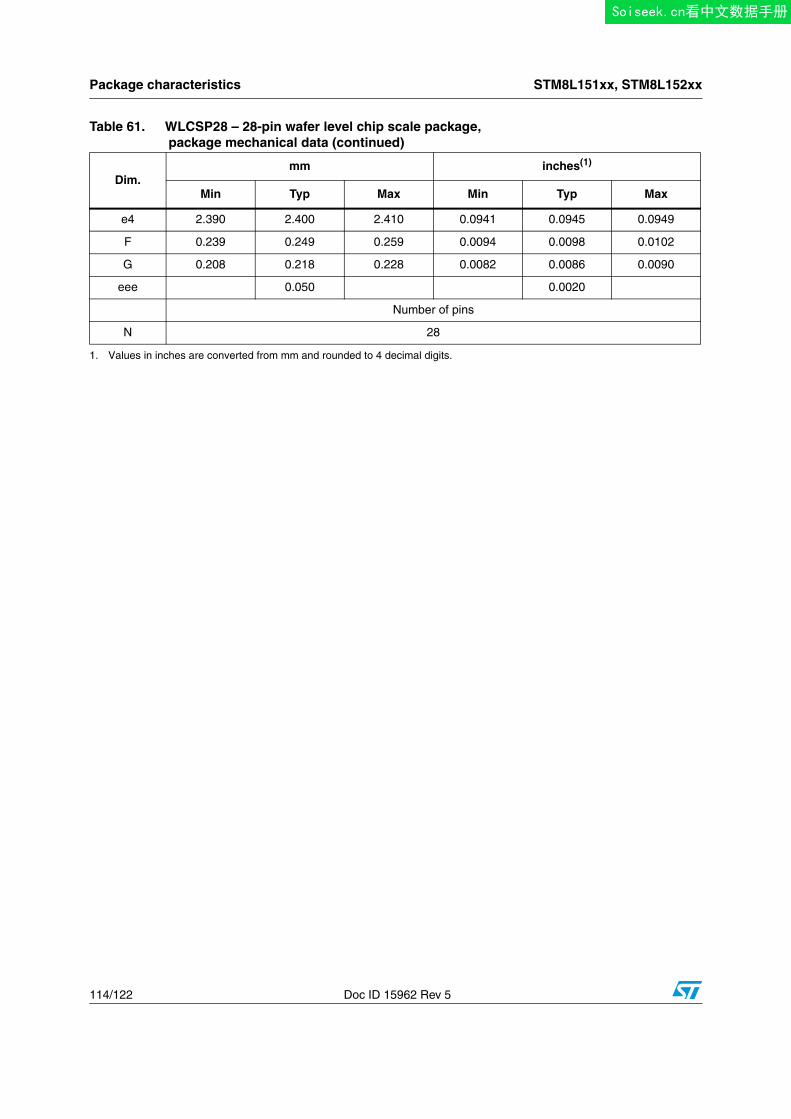
Package characteristics STM8L151xx, STM8L152xx
114/122 Doc ID 15962 Rev 5
e4 2.390 2.400 2.410 0.0941 0.0945 0.0949
F 0.239 0.249 0.259 0.0094 0.0098 0.0102
G 0.208 0.218 0.228 0.0082 0.0086 0.0090
eee 0.050 0.0020
Number of pins
N 28
1. Values in inches are converted from mm and rounded to 4 decimal digits.
Table 61. WLCSP28 – 28-pin wafer level chip scale package, package mechanical data (continued)
Dim.mm inches(1)
Min Typ Max Min Typ Max
Soiseek.cn看中文数据手册
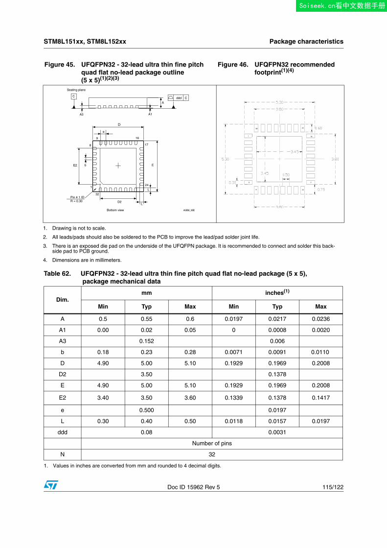
STM8L151xx, STM8L152xx Package characteristics
Doc ID 15962 Rev 5 115/122
Figure 45. UFQFPN32 - 32-lead ultra thin fine pitch quad flat no-lead package outline (5 x 5)(1)(2)(3)
Figure 46. UFQFPN32 recommended footprint(1)(4)
1. Drawing is not to scale.
2. All leads/pads should also be soldered to the PCB to improve the lead/pad solder joint life.
3. There is an exposed die pad on the underside of the UFQFPN package. It is recommended to connect and solder this back-side pad to PCB ground.
4. Dimensions are in millimeters.
Seating plane
ddd CC
A3 A1
A
D
e
9 16
17
24
32Pin # 1 IDR = 0.30
8
E
L
L
D2
1
bE2
A0B8_ME
Bottom view
Table 62. UFQFPN32 - 32-lead ultra thin fine pitch quad flat no-lead package (5 x 5), package mechanical data
Dim.mm inches(1)
Min Typ Max Min Typ Max
A 0.5 0.55 0.6 0.0197 0.0217 0.0236
A1 0.00 0.02 0.05 0 0.0008 0.0020
A3 0.152 0.006
b 0.18 0.23 0.28 0.0071 0.0091 0.0110
D 4.90 5.00 5.10 0.1929 0.1969 0.2008
D2 3.50 0.1378
E 4.90 5.00 5.10 0.1929 0.1969 0.2008
E2 3.40 3.50 3.60 0.1339 0.1378 0.1417
e 0.500 0.0197
L 0.30 0.40 0.50 0.0118 0.0157 0.0197
ddd 0.08 0.0031
Number of pins
N 32
1. Values in inches are converted from mm and rounded to 4 decimal digits.
Soiseek.cn看中文数据手册
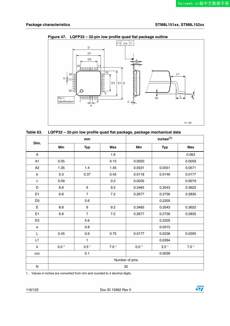
Package characteristics STM8L151xx, STM8L152xx
116/122 Doc ID 15962 Rev 5
Figure 47. LQFP32 – 32-pin low profile quad flat package outline
5V_ME
LA1 K
L1
c
AA2
ccc C
D
D1
D3
E3 E1 E
16
1724
25
b
32
1Pin 1identification 8
9
Table 63. LQFP32 – 32-pin low profile quad flat package, package mechanical data
Dim.mm inches(1)
Min Typ Max Min Typ Max
A 1.6 0.063
A1 0.05 0.15 0.0020 0.0059
A2 1.35 1.4 1.45 0.0531 0.0551 0.0571
b 0.3 0.37 0.45 0.0118 0.0146 0.0177
c 0.09 0.2 0.0035 0.0079
D 8.8 9 9.2 0.3465 0.3543 0.3622
D1 6.8 7 7.2 0.2677 0.2756 0.2835
D3 5.6 0.2205
E 8.8 9 9.2 0.3465 0.3543 0.3622
E1 6.8 7 7.2 0.2677 0.2756 0.2835
E3 5.6 0.2205
e 0.8 0.0315
L 0.45 0.6 0.75 0.0177 0.0236 0.0295
L1 1 0.0394
k 0.0 ° 3.5 ° 7.0 ° 0.0 ° 3.5 ° 7.0 °
ccc 0.1 0.0039
Number of pins
N 32
1. Values in inches are converted from mm and rounded to 4 decimal digits.
Soiseek.cn看中文数据手册
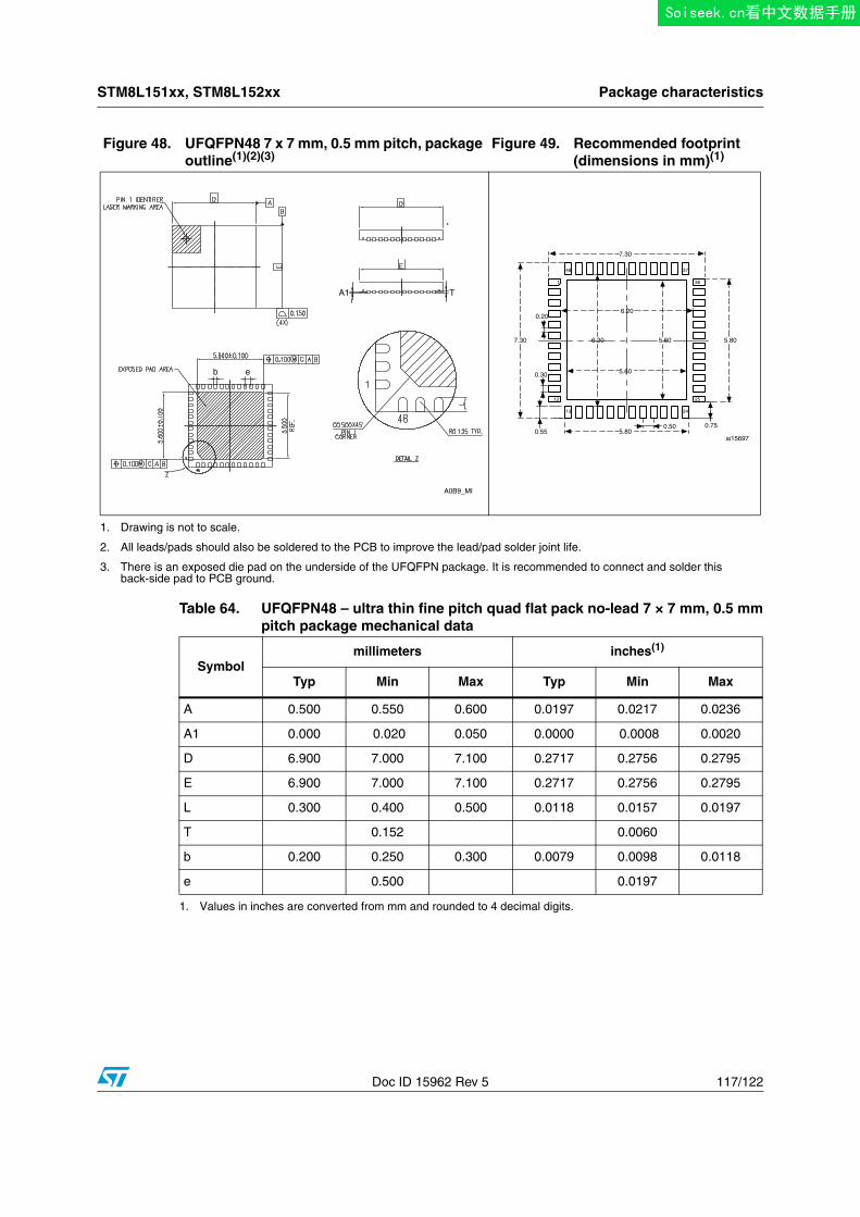
STM8L151xx, STM8L152xx Package characteristics
Doc ID 15962 Rev 5 117/122
Figure 48. UFQFPN48 7 x 7 mm, 0.5 mm pitch, package outline(1)(2)(3)
Figure 49. Recommended footprint (dimensions in mm)(1)
1. Drawing is not to scale.
2. All leads/pads should also be soldered to the PCB to improve the lead/pad solder joint life.
3. There is an exposed die pad on the underside of the UFQFPN package. It is recommended to connect and solder this back-side pad to PCB ground.
7.30
7.30
0.20
0.30
0.550.50
5.80
6.20
6.20 5.60
5.60
5.80
0.75
ai15697
48
1
12
13 24
25
36
37
Table 64. UFQFPN48 – ultra thin fine pitch quad flat pack no-lead 7 × 7 mm, 0.5 mmpitch package mechanical data
Symbolmillimeters inches(1)
1. Values in inches are converted from mm and rounded to 4 decimal digits.
Typ Min Max Typ Min Max
A 0.500 0.550 0.600 0.0197 0.0217 0.0236
A1 0.000 0.020 0.050 0.0000 0.0008 0.0020
D 6.900 7.000 7.100 0.2717 0.2756 0.2795
E 6.900 7.000 7.100 0.2717 0.2756 0.2795
L 0.300 0.400 0.500 0.0118 0.0157 0.0197
T 0.152 0.0060
b 0.200 0.250 0.300 0.0079 0.0098 0.0118
e 0.500 0.0197
Soiseek.cn看中文数据手册
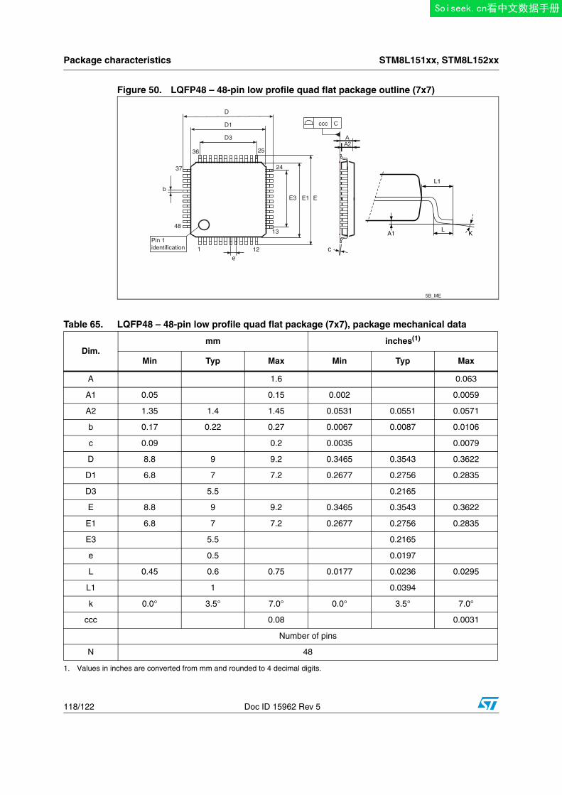
Package characteristics STM8L151xx, STM8L152xx
118/122 Doc ID 15962 Rev 5
Figure 50. LQFP48 – 48-pin low profile quad flat package outline (7x7)
5B_ME
LA1 K
L1
c
AA2
ccc C
D
D1
D3
E3 E1 E
24
2536
37
b
48
1
Pin 1identification 12
13
Table 65. LQFP48 – 48-pin low profile quad flat package (7x7), package mechanical data
Dim.mm inches(1)
Min Typ Max Min Typ Max
A 1.6 0.063
A1 0.05 0.15 0.002 0.0059
A2 1.35 1.4 1.45 0.0531 0.0551 0.0571
b 0.17 0.22 0.27 0.0067 0.0087 0.0106
c 0.09 0.2 0.0035 0.0079
D 8.8 9 9.2 0.3465 0.3543 0.3622
D1 6.8 7 7.2 0.2677 0.2756 0.2835
D3 5.5 0.2165
E 8.8 9 9.2 0.3465 0.3543 0.3622
E1 6.8 7 7.2 0.2677 0.2756 0.2835
E3 5.5 0.2165
e 0.5 0.0197
L 0.45 0.6 0.75 0.0177 0.0236 0.0295
L1 1 0.0394
k 0.0° 3.5° 7.0° 0.0° 3.5° 7.0°
ccc 0.08 0.0031
Number of pins
N 48
1. Values in inches are converted from mm and rounded to 4 decimal digits.
Soiseek.cn看中文数据手册
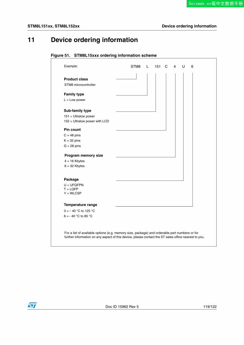
STM8L151xx, STM8L152xx Device ordering information
Doc ID 15962 Rev 5 119/122
11 Device ordering information
Figure 51. STM8L15xxx ordering information scheme
STM8 L 151 C 4 U 6
Product classSTM8 microcontroller
Pin countC = 48 pins
K = 32 pins
G = 28 pins
PackageU = UFQFPNT = LQFPY = WLCSP
Example:
Sub-family type151 = Ultralow power
152 = Ultralow power with LCD
Family typeL = Low power
Temperature range
3 = - 40 °C to 125 °C
6 = - 40 °C to 85 °C
For a list of available options (e.g. memory size, package) and orderable part numbers or for further information on any aspect of this device, please contact the ST sales office nearest to you.
Program memory size4 = 16 Kbytes
6 = 32 Kbytes
Soiseek.cn看中文数据手册
Revision history STM8L151xx, STM8L152xx
120/122 Doc ID 15962 Rev 5
12 Revision history
Table 66. Document revision history
Date Revision Changes
06-Aug-2009 1 Initial release
10-Sep-2009 2
Updated peripheral naming throughout document.Added Figure 7: STM8L151Cx 48-pin pinout (without LCD) on page 25
Added capacitive sensing channels in Features on page 1Updated PA7, PC0 and PC1 in Table 5: STM8L15x pin description
Changed CLK and REMAP register names in Table 8
Changed description of WDGHALT in Table 12Added typical power consumption values in Table 18 to Table 26
Correct VIH max in Table 36
11-Dec-2009 3
Added WLCSP28 packageModified Figure 9: Memory map on page 35 and added 2 notes.Modified Low power run mode in Section 3.1: Low power modes on page 14Added Section 8: Unique ID on page 59Modified Table 10: Interrupt mapping on page 54 (added reserved area at address 0x00 8008)Modified OPT4 option bits in Table 11: Option byte addresses on page 56Table 12: Option byte description on page 57: modified OPT0 description (“disable” instead of “enable”) and OPT1 descriptionAdded OPTBL option bytesModified Section 9: Electrical parameters on page 60
02-Apr-2010 4
Changed title of the document (STM8L151x4, STM8L151x6, STM8L152x4, STM8L152x6)Changed pinout (VSS1, VDD1, VSS2, VDD 2 instead of VSS, VDD, VSSIO, VDDIOChanged packagesChanged first pageModified note 1 in Table 5: STM8L15x pin description on page 27Added note to PA7, PC0, PC1 and PE0 in Table 5: STM8L15x pin description on page 27Modified Figure 9: Memory map on page 35Modified Table 61: WLCSP28 – 28-pin wafer level chip scale package, package mechanical data on page 113 (min and max columns swapped)Modified Figure 44: WLCSP28 – 28-pin wafer level chip scale package, package outline on page 113 (A1 ball location)Section : on page 79: renamed Rm, Lm and CmEXTI_CONF replaced with EXTI_CONF1 in Table 8: General hardware register map on page 37Updated Section 9: Electrical parameters on page 60
Soiseek.cn看中文数据手册
STM8L151xx, STM8L152xx Revision history
Doc ID 15962 Rev 5 121/122
23-Jul-2010 5
Modified Introduction and DescriptionModified Table 4: Legend/abbreviation for table 5 on page 27 and Table 5: STM8L15x pin description on page 27 (for PA0, PA1, PB0 and PB4 and for reset states in the floating input column)Modified Figure 1: STM8L15xxx device block diagram on page 13 and Figure 2: STM8L15x clock tree diagram on page 18Modified Figure 3.1: Low power modes on page 14 and Figure 3.5: Low power real-time clock on page 18Modified CLK_PCKENR2 and CLK_HSICALR reset values in Table 8: General hardware register map on page 37Modified notes below Figure 9: Memory map on page 35Modified PA_CR1 reset value in Table 7 on page 36Modified reset values for Px_IDR registers in Table 7 on page 36Modified Table 14: Voltage characteristics on page 61, Table 15: Current characteristics on page 62Modified VIH in Table 36: I/O static characteristics on page 85Modified Table 20: Total current consumption in Wait mode on page 69Modified Figure 37: Typical application with I2C bus and timing diagram 1) on page 96Modified IL value in Figure 39: Typical connection diagram using the ADC on page 105Modified RH and RL in Table 43: LCD characteristics on page 97Added graphs in Section 9: Electrical parameters on page 60Modified note 3 below Table 44: Reference voltage characteristics on page 98Added notes to Modified note 1 below Table 45: TS characteristics on page 99Changed VESD(CDM) value in Table 57 on page 108Modified notes or added notes below UFQFPN32 and UFQFPN48 packages
Table 66. Document revision history
Date Revision Changes
Soiseek.cn看中文数据手册
STM8L151xx, STM8L152xx
122/122 Doc ID 15962 Rev 5
Please Read Carefully:
Information in this document is provided solely in connection with ST products. STMicroelectronics NV and its subsidiaries (“ST”) reserve theright to make changes, corrections, modifications or improvements, to this document, and the products and services described herein at anytime, without notice.
All ST products are sold pursuant to ST’s terms and conditions of sale.
Purchasers are solely responsible for the choice, selection and use of the ST products and services described herein, and ST assumes noliability whatsoever relating to the choice, selection or use of the ST products and services described herein.
No license, express or implied, by estoppel or otherwise, to any intellectual property rights is granted under this document. If any part of thisdocument refers to any third party products or services it shall not be deemed a license grant by ST for the use of such third party productsor services, or any intellectual property contained therein or considered as a warranty covering the use in any manner whatsoever of suchthird party products or services or any intellectual property contained therein.
UNLESS OTHERWISE SET FORTH IN ST’S TERMS AND CONDITIONS OF SALE ST DISCLAIMS ANY EXPRESS OR IMPLIEDWARRANTY WITH RESPECT TO THE USE AND/OR SALE OF ST PRODUCTS INCLUDING WITHOUT LIMITATION IMPLIEDWARRANTIES OF MERCHANTABILITY, FITNESS FOR A PARTICULAR PURPOSE (AND THEIR EQUIVALENTS UNDER THE LAWSOF ANY JURISDICTION), OR INFRINGEMENT OF ANY PATENT, COPYRIGHT OR OTHER INTELLECTUAL PROPERTY RIGHT.
UNLESS EXPRESSLY APPROVED IN WRITING BY AN AUTHORIZED ST REPRESENTATIVE, ST PRODUCTS ARE NOTRECOMMENDED, AUTHORIZED OR WARRANTED FOR USE IN MILITARY, AIR CRAFT, SPACE, LIFE SAVING, OR LIFE SUSTAININGAPPLICATIONS, NOR IN PRODUCTS OR SYSTEMS WHERE FAILURE OR MALFUNCTION MAY RESULT IN PERSONAL INJURY,DEATH, OR SEVERE PROPERTY OR ENVIRONMENTAL DAMAGE. ST PRODUCTS WHICH ARE NOT SPECIFIED AS "AUTOMOTIVEGRADE" MAY ONLY BE USED IN AUTOMOTIVE APPLICATIONS AT USER’S OWN RISK.
Resale of ST products with provisions different from the statements and/or technical features set forth in this document shall immediately voidany warranty granted by ST for the ST product or service described herein and shall not create or extend in any manner whatsoever, anyliability of ST.
ST and the ST logo are trademarks or registered trademarks of ST in various countries.
Information in this document supersedes and replaces all information previously supplied.
The ST logo is a registered trademark of STMicroelectronics. All other names are the property of their respective owners.
© 2010 STMicroelectronics - All rights reserved
STMicroelectronics group of companies
Australia - Belgium - Brazil - Canada - China - Czech Republic - Finland - France - Germany - Hong Kong - India - Israel - Italy - Japan - Malaysia - Malta - Morocco - Philippines - Singapore - Spain - Sweden - Switzerland - United Kingdom - United States of America
www.st.com
Soiseek.cn看中文数据手册


![[ 搜 索 引 擎 ]](https://static.fdocument.pub/doc/165x107/56813ea4550346895da8fa2b/-56813ea4550346895da8fa2b.jpg)