SERVICE MANUAL FOR
178
BY: Grass Grass .Ren .Ren Repair Technology Research Department /EDVD Repair Technology Research Department /EDVD Feb.2004 SERVICE MANUAL FOR 8050
Transcript of SERVICE MANUAL FOR

BY: GrassGrass.Ren.Ren
Repair Technology Research Department /EDVDRepair Technology Research Department /EDVDFeb.2004
SERVICE MANUAL FOR
8050
8050 8050 N/B MaintenanceN/B Maintenance
1
1. Hardware Engineering Specification …………………………………………………………………..1.1 Introduce……………………………………………………………………………………………….1.2 System Overview……………………………………………………………………………………….1.3 System Hardware Parts………………………………………………………………………………....
2. System View & Disassembly …………………………………………………………………………..2.1 System View …………………………………………………………………………………………...2.2 System Disassembly…………………………………………………………………………………….
3. Definition & Location of Connectors / Switches Setting ………………………………………………
4. Definition & Location of Major Component …………………………………………………………..
5. Pin Description of Major Component…………………………………………………………………..5.1 Pentium4 (Willamette/Northwood) processor …………………………………………………………...5.2 Sis650 North Bridge…………………………………………………………………………………….5.3 Sis962 South Bridge…………………………………………………………………………………….
6. System Block Diagram ……………………………………………………….………………………….
7. Maintenance Diagnostics ………………………………………………………………………………..7.1 Introduction……………………………………………………………………………………………7.2 Debug Card……………………………………………………………………………………………7.3 Error code……………………………………………………………………………………………..
Contents
3
3
6
9
34
37
57
60
62
6266
75
83
84
84
86
85
34
8050 8050 N/B MaintenanceN/B Maintenance
2
8. Trouble Shooting …………………………………………………………………………………………8.1 No Power ……………………………………………………………………………………………….8.2 Battery Can not Be Charged…………………………………………………………………………….8.3 No Display……………………………………………………………………………………………..8.4 External Monitor No Display………………………………………………………………………….... 8.5 Memory Test Error ……………………………………………………………………………………. 8.6 Keyboard/Touch-pad Test Error ………………………………………………………………………..8.7 USB Port Test error……………………………………………………………………………………..8.8 Hard Disk Drive Test Error……………………………………………………………………………...8.9 CD-ROM Test Error……………………………………………………………………………………8.10 Audio Test Failure……………………………………………………………………………………..8.11 LAN Test Error……………………………………………………………………………………….8.12 Modem Test Error…………………………………………………………………………………….8.13 Mini-PCI Test Error……….. ………………………………………………………………………...8.14 Card Bus&Reader Test Error…………………………………………………………………………..8.15 TV Encoder Test Failure ………………………………………………………….…………………8.16 IEEE1394 Test Failure …………………………………………………………………………….…..
9. Spare Parts List ………………………………………………………………………………………….
10. System Exploded View …………………………………………………………………………………
11. Circuit Diagram ………………………………………………………………………………………..
12. Reference Material …………………………………………………………………………………….
Contents
89
90
9597
103
105
107109
111113
115
118
120122
124126
128
141
142
130
176
8050 8050 N/B MaintenanceN/B Maintenance
3
1.1 Introduce
1. Engineer Hardware Specification
The MiTAC 8050 model is designed for Intel Banias processor with 400MHz FSB with Micro-FCPGA package. It can support Banias 1.5G ~ 1.9GHz/Dothan 2.0GHz and above.
This system is based on PCI architecture and is fully compatible with IBM PC/AT specification, which has standard hardware peripheral interface. The power management complies with Advanced Configuration and Power Interface (ACPI) 2.0. It also provides easy configuration through CMOS setup, which is built in system BIOS software and can be pop-up by pressing F2 key at system start up or warm reset. System also provides icon LEDs to display system status, such as AC Power indicator, Battery Power indicator, Battery status indicator, HDD,CD-ROM, NUM LOCK, CAP LOCK, SCROLL LOCK, RF on/off Card Reader indicator. It also equipped with LAN, 56K Fax MODEM, 3 USB port, S-Video and audio line in/out , external microphone function.
The memory subsystem supports two expansion DDR SDRAM slot with unbuffered PC1600/PC2100 DDR-SDRAM.
The Montara-GME GMCH Host Memory Controller integrates a high performance host interface for Intel Banias processor, a high performance 2D/3D Graphic Engine, a high performance memory controller, Digital Video port (DVOB & DVOC) interface, and Intel Hub interface Technology connecting with Intel 82801DBM ICH4-M.
The Intel ICH4-M integrates three Universal Serial Bus 2.0 Host Controllers Interface (UHCI), the Audio Controller with AC97 interface, the Ethernet includes a 32-bit PCI controller, the IDE Master/Slave controllers,
8050 8050 N/B MaintenanceN/B Maintenance
4
and Intel Hub interface technology.
The MOBILITY M10 provides one of the fastest and most advanced 2D, 3D, and multimedia graphics2performance for notebooks. It’s architecture introduces the latest achievements in the graphics industry, which enable the use of the progressive new features in upcoming applications, but without compromising performance. ATIs support of support of DirectX® 9 features, highly optimized Open GL® support, and flexible memory configurations allow implementations targeted at the gaming enthusiast, consumer, business and workstation platforms.
The Realtek RTL8100C(L) is a highly integrated, cost-effective single-chip Fast Ethernet controller that provides 32-bit performance, PCI bus master capability, and full compliance with IEEE 802.3u 100Base-T specifications and IEEE 802.3x Full Duplex Flow Control. It also supports the Advanced Configuration Power management Interface (ACPI).
The VT6307L is a single chip PCI Host Controller for IEEE 1394-1995 Release 1.0 and IEEE 1394a P2000. It implements the Link and PHY layers for IEEE 1394-1995 High Performance Serial Bus specification release 1.0 and 1394a P2000. It is compliant with 1394 Open HCI 1.0 and 1.1 with DMA engine support for high performance data transfer via a 32-bit bus master PCEI host bus interface. The VT6307L supports 100, 200 and 400 Mbit/sec transmission via an integrated 2-port PHY. The VT6307L services two types of data packets: asynchronous and isochronous(real time). The 1394 link core performs arbitration requesting, packet generation and checking, and bus cycle master operations. It also has root node capability and performs retry operations.
The RICOH R5C592 CardBus/Media Reader controller functions as a single slot PCI to Cardbus bridge and also PCI interface smart card and MS/SD/MMC flash card reader. The R5C592 provide one Cardbus slot and all reader interface may operate simultaneously.
8050 8050 N/B MaintenanceN/B Maintenance
5
The CH7011A is a display controller device which accepts a digital graphics input signal, and encodes and transmits data to a TV output (analog composite, s-video or RGB). The device accepts data over one 12-bit wide variable voltage data port which supports five different data format including RGB and YcrCb. The TV-Out processor will perform non-interlace to interlace conversion with scaling and flicker filters, and encode the data into any of the NTSC or PAL video standards. The scaling and flicker filter is adaptive and programmable to enable superior text display. Eight graphics resolutions are supported up to 1024 X 768 with full vertical and horizontal underscan capability in all modes. A high accuracy low jitter phase locked loop is integrated to create outstanding video quality. Support is provided for Macrovision and RGB bypass mode which enable driving a VGA CRT with the input data.
The W83L950D is a high performance microcontroller on-chip supporting functions optimized for embedded control.These include ROM, RAM, four types of timers, a serial communication interface, optional I²C bus interface, host interface, A/D converter, D/A converter, I/O ports, and other functions needed in control system configurations, so that compact, high performance systems can be implemented easily.
A full set of software drivers and utilities are available to allow advanced operating systems such as Windows ME, Windows 2000 and Windows XP to take full advantage of the hardware capabilities. Features such as bus mastering IDE, Plug and Play, Advanced Power Management (APM) with application restart, software-controlled power shutdown.
Following chapters will have more detail description for each individual sub-systems and functions.
8050 8050 N/B MaintenanceN/B Maintenance
6
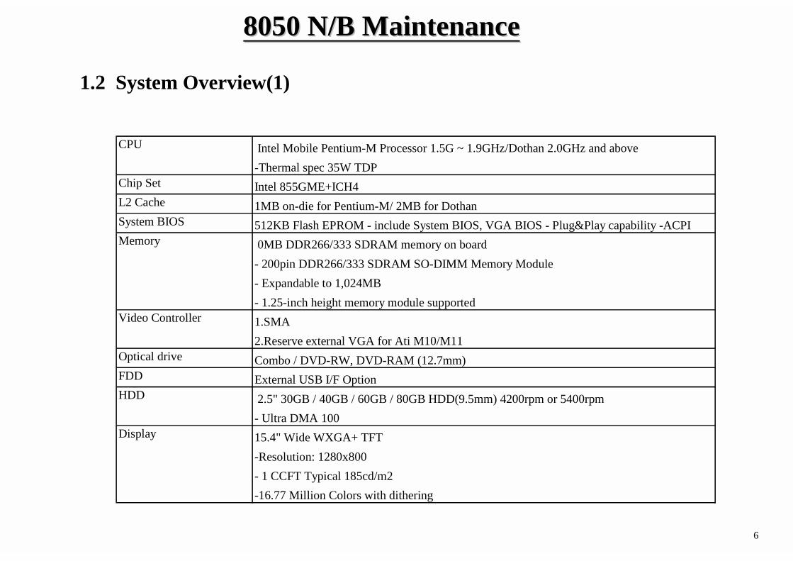
1.2 System Overview(1)
Intel Mobile Pentium-M Processor 1.5G ~ 1.9GHz/Dothan 2.0GHz and above-Thermal spec 35W TDP
Chip Set Intel 855GME+ICH4L2 Cache 1MB on-die for Pentium-M/ 2MB for DothanSystem BIOS 512KB Flash EPROM - include System BIOS, VGA BIOS - Plug&Play capability -ACPI
0MB DDR266/333 SDRAM memory on board- 200pin DDR266/333 SDRAM SO-DIMM Memory Module- Expandable to 1,024MB- 1.25-inch height memory module supported1.SMA2.Reserve external VGA for Ati M10/M11
Optical drive Combo / DVD-RW, DVD-RAM (12.7mm)FDD External USB I/F Option
2.5" 30GB / 40GB / 60GB / 80GB HDD(9.5mm) 4200rpm or 5400rpm- Ultra DMA 10015.4" Wide WXGA+ TFT-Resolution: 1280x800- 1 CCFT Typical 185cd/m2-16.77 Million Colors with dithering
CPU
Memory
Video Controller
HDD
Display
8050 8050 N/B MaintenanceN/B Maintenance
8
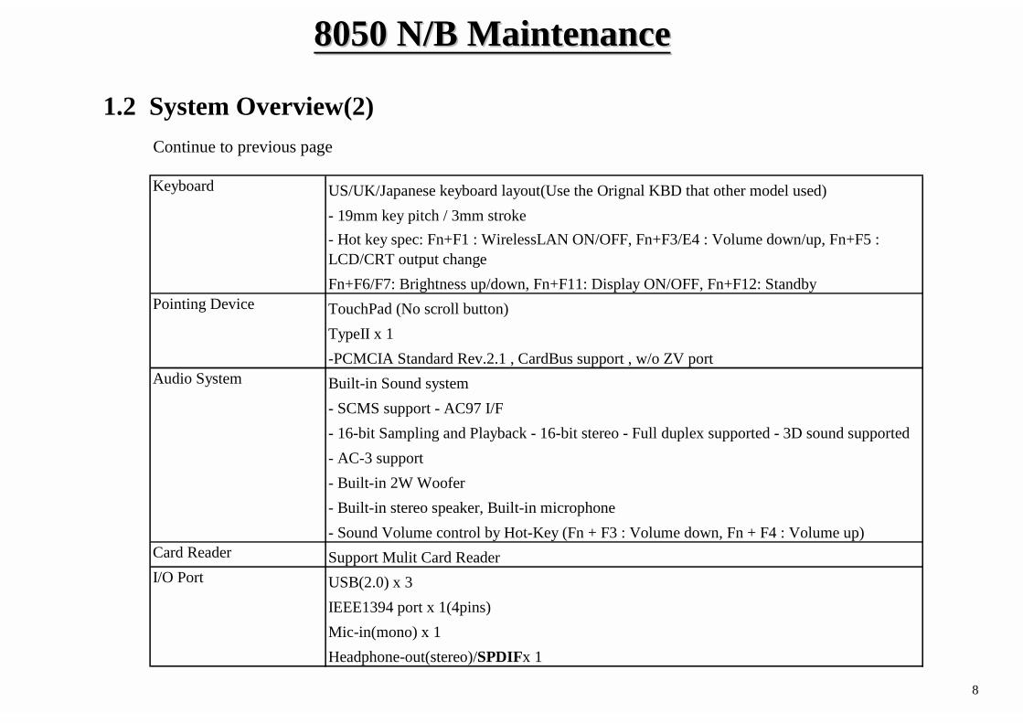
1.2 System Overview(2)Continue to previous page
US/UK/Japanese keyboard layout(Use the Orignal KBD that other model used)- 19mm key pitch / 3mm stroke- Hot key spec: Fn+F1 : WirelessLAN ON/OFF, Fn+F3/E4 : Volume down/up, Fn+F5 :LCD/CRT output changeFn+F6/F7: Brightness up/down, Fn+F11: Display ON/OFF, Fn+F12: StandbyTouchPad (No scroll button)TypeII x 1-PCMCIA Standard Rev.2.1 , CardBus support , w/o ZV portBuilt-in Sound system- SCMS support - AC97 I/F- 16-bit Sampling and Playback - 16-bit stereo - Full duplex supported - 3D sound supported- AC-3 support- Built-in 2W Woofer- Built-in stereo speaker, Built-in microphone- Sound Volume control by Hot-Key (Fn + F3 : Volume down, Fn + F4 : Volume up)
Card Reader Support Mulit Card ReaderUSB(2.0) x 3IEEE1394 port x 1(4pins)Mic-in(mono) x 1Headphone-out(stereo)/SPDIFx 1
Keyboard
Pointing Device
Audio System
I/O Port
8050 8050 N/B MaintenanceN/B Maintenance
8
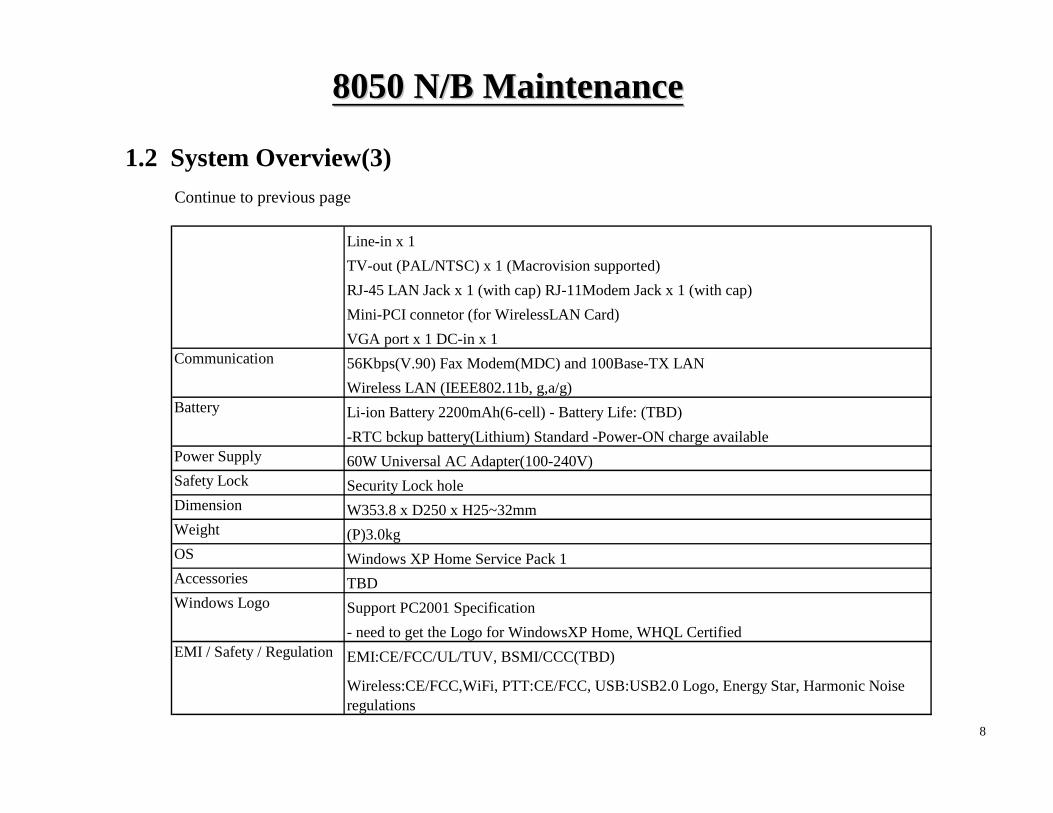
Line-in x 1TV-out (PAL/NTSC) x 1 (Macrovision supported)RJ-45 LAN Jack x 1 (with cap) RJ-11Modem Jack x 1 (with cap)Mini-PCI connetor (for WirelessLAN Card)VGA port x 1 DC-in x 156Kbps(V.90) Fax Modem(MDC) and 100Base-TX LANWireless LAN (IEEE802.11b, g,a/g)Li-ion Battery 2200mAh(6-cell) - Battery Life: (TBD)-RTC bckup battery(Lithium) Standard -Power-ON charge available
Power Supply 60W Universal AC Adapter(100-240V)Safety Lock Security Lock holeDimension W353.8 x D250 x H25~32mmWeight (P)3.0kgOS Windows XP Home Service Pack 1Accessories TBDWindows Logo Support PC2001 Specification
- need to get the Logo for WindowsXP Home, WHQL CertifiedEMI:CE/FCC/UL/TUV, BSMI/CCC(TBD)
Wireless:CE/FCC,WiFi, PTT:CE/FCC, USB:USB2.0 Logo, Energy Star, Harmonic Noiseregulations
Communication
Battery
EMI / Safety / Regulation
1.2 System Overview(3)Continue to previous page
8050 8050 N/B MaintenanceN/B Maintenance
9
1.3.1 Intel Banias processors in Micro-FCPGA package.
Intel Banias Processors with 478 pins Micro-FCPGA package.
The first Intel mobile processor with the Intel NetBurst micro-architecture which features include hyper-pipelined technology, a rapid execution engine, a 400MHz system, an execution trace cache, advanced dynamic execution, advanced transfer cache, enhanced floating point and multi-media unit, and Streaming SIMD Extensions 2 (SSE2).
The Streaming SIMD Extensions 2 (SSE2) enable break-through levels of performance in multimedia applications including 3-D graphics, video decoding/encoding, and speech recognition.
Use Source-Synchronous Transfer (SST) of address and data to improve performance by transferring data four times per bus clock.
Support Enhanced Intel SpeedStep technology, which enables real-time dynamic switching of the voltage and frequency between two performance modes.
1.3.2 Clock Generator
System frequency synthesizer: ICS950810 Programmable output frequency, divider ratios, output rise/fall time,
1.3 System Hardware Parts
8050 8050 N/B MaintenanceN/B Maintenance
10
1.3.3 Montara-GME GMCH IGUI 3D Graphic DDR/SDR Chipset
output skew. Programmable spread percentage for EMI control. Watchdog timer technology to reset system if system malfunctions. Programmable watchdog safe frequency. Support I2C Index read/write and block read/write operations. Use external 14.318MHz crystal.
Montara-GME GMCH IGUI Host Memory Controller integrates a high performance host interface for Intel Banias processor, a high performance 2D/3D Graphic Engine, a high performance memory controller, an AGP 4X interface, and Intel®’ I/O Hub architecture INTEL 82801DBM ICH4-M.
Montara-GME GMCH Host Interface features the AGTL & AGTL+ compliant bus driver technology with integrated on-die termination to support Intel Banias processors. Montara-GME GMCH provides a 12-deep In-Order-Queue to support maximum outstanding transactions up to 12. It integrated a high performance 2D/3D Graphic Engine, Video Accelerator and Advanced Hardware Acceleration MPEGI/MPEGII Video Decoder for the Intel Banias series based PC systems. It also integrates a high performance 2.1GB/s DDR266 Memory controller to sustain the bandwidth demand from the integrated GUI or external AGP master, host processor, as well as the multi I/O masters. In addition to integrated GUI, Montara-GME GMCH also can support external AGP slot with AGP 1X/2X/4X capability and Fast Write Transactions. A high bandwidth and mature Intel®’ I/O Hub architecture is incorporated to connect Montara-GME GMCH and INTEL 82801DBM ICH4-Mtogether. Intel®’I/O Hub architecture is developed into three layers, the Multi-threaded I/O Link Layer delivering 1.2GB bandwidth to connect embedded DMA Master devices and external PCI masters to interface to Multi-threaded I/O Link layer, the Multi-threaded I/O Link Encoder/Decoder in INTEL 82801DBM ICH4-M to transfer data w/ 533 MB/s bandwidth
8050 8050 N/B MaintenanceN/B Maintenance
11
Features
Processor/Host Bus Support
from/to Multi-threaded I/O Link layer to/from Montara-GME GMCH, and the Multi-threaded I/O Link Encoder/Decoder in Montara-GME GMCH to transfer data w/ 533 MB/s from/to Multi-threaded I/O Link layer to/from INTEL 82801DBM ICH4-M.
An Unified Memory Controller supporting DDR266 DRAM is incorporated, delivering a high performance data transfer to/from memory subsystem from/to the Host processor, the integrated graphic engine or external AGP master, or the I/O bus masters. The memory controller also supports the Suspend to RAM function by retaining the CKE# pins asserted in ACPI S3 state in which only AUX source deliver power. The Montara-GME GMCH adopts the Shared Memory Architecture, eliminating the need and thus the cost of the frame buffer memory by organizing the frame buffer in the system memory. The frame buffer size can be allocated from 8MB to 64MB.
Intel® Banias processor
Support host bus Dynamic Bus Inversion (DBI)
2X Address, 4X data
Supports system bus at 400MT/s (100 MHz) Supports 64-bit host bus addressing
8-deep In-Order-Queue
8050 8050 N/B MaintenanceN/B Maintenance
12
AGTL+ bus driver technology with integrated GTL termination resistors and low voltage operation (1.05V)
Supports Enhanced Intel® Speed Step TM Technology (EIST) and Geyserville III
Support for DPWR# signal to Banias processor for PSB power management
Memory System
Directly supports one DDR channel, 64-bts wide (72-b with ECC).
Supports 200-MHz and 266-MHz DDR devices with max of 2 Double-Sided SO-DIMMs(4 rows populated) with unbuffered PC1600/PC2100 DDR(with ECC).
Supports 128-Mb, 256-Mb and 512-Mbit technologies providing maximum capacity of 1-GB with only x 16 devices.
All supported devices have 4 banks.
Supports up to 16 simultaneous open pages.
Supports page sizes of 2KB, 4KB, 8KB, and 16KB. Page size is individually selected for every row. UMA support only.
System Interrupt
8050 8050 N/B MaintenanceN/B Maintenance
13
Supports 8259 and Processor
System Bus interrupt delivery mechanism
Supports interrupts signaled as upstream Memory Writes from PCI and Hub interface
MSI sent to the CPU through the system Bus
From IOxAPIC in ICH4-M
Provides redirection for upstream interrupts to the System Bus
Video Stream Decoder
Improved HW Motion Compensation for MPEG2
All format decoder (18 ATSC formats) supported Dynamic Bob and Weave support for Video Streams
Software DVD at 60 fields/second and 30 frames/second full screen
Support for 720x480 pixel resolution DVD quality encoding at low CPU utilization Video Overlay
Single high quality scalable overlay and second Sprite to support second overlay
Multiple overlay functionality provided via Arithmetic Stretch Blt
Direct YUV from Overlay to TV-out
8050 8050 N/B MaintenanceN/B Maintenance
14
Independent Gamma Correction
Independent Brightness / Contrast / Saturation
Independent Tint / Hue support
Destination Color keying
Source Chroma keying
Maximum source resolution of 1920x1080 pixels
Maximum overlay clock of 133 MHz/200 MHz provides a pixel resolution up to 1600x1200@ 60Hz or 1280x1024@ 85 Hz
Analog Display Support 350 MHz integrated 24-bit RAMDAC that can drive a standard progressive scan analog monitor up to 1800x1350 @ 85 Hz accompanying I2C and DDC channels provided through multiplexed interface hot plug and display support
Dual independent pipe with single display support Simultaneous: Same images and native display timings on each display device
DVO (DVOB) support
Digital video out port DVOB with 165-MHz dot clock on 12-bit interface
Display
8050 8050 N/B MaintenanceN/B Maintenance
15
Variety of DVO devices channel
Compliant with DVI Specification 1.0, thereby providing support for a flat panel up to 2048x1536 pixel resolution, or digital CRT up to 1920x1080 pixel resolution
1.3.4 I/O Controller Hub : INTEL 82801DBM
The INTEL 82801DBM ICH4-M integrates three Universal Serial Bus 2.0 Host Controllers, the Audio Controller with AC 97 Interface, the IDE Master/Slave controllers, and Intel®’ I/O Hub architecture. The PCI to LPC Bridge, I/O Advanced Programmable Interrupt Controller, legacy system I/O and legacy power management functionalities are integrated as well.
The integrated Universal Serial Bus Host Controllers features Dual Independent UHCI Compliant Host controllers with six USB ports delivering 480 Mb/s bandwidth and rich connectivity. Besides, Legacy USB devices as well as over current detection are also implemented.
The Integrated AC97 v2.3 compliance Audio Controller that features a 7-channels of audio speaker out and HSP v.90 modem support. Additionally, the AC97 interface supports 4 separate SDATAIN pins that is capable of supporting multiple audio codecs with one separate modem codec.
The integrated IDE Master/Slave controllers features Dual Independent IDE channels supporting PIO mode transfers up to 16 Mbytes/sec and Ultra DMA 33/66/100. It provides two separate data paths for the dual IDE channels that sustain the high data transfer rate in the multitasking environment.
8050 8050 N/B MaintenanceN/B Maintenance
16
INTEL 82801DBM ICH4-M supports 6 PCI masters and complies with PCI 2.2 specification. It also incorporates the legacy system I/O like: two 82C37 compatible DMA controllers, Channels 0-3 are hardwired to 8 bit, three 8254 compatible programmable 16-bit counters channels 5-7, hardwired keyboard controller and PS2 mouse interface(not use in MiTAC 8050 model), Real Time clock with 512Bytes CMOS SRAM and two 82C59 compatible Interrupt controllers. Besides, the I/O APIC managing up to 14 interrupts with both Serial and FSB interrupt delivery modes is supported.
The integrated power management module incorporates the ACPI 1.0b compliance functions, the APM 1.2 compliance functions, and the PCI bus power management interface spec. v1.1. Numerous power-up events and power down events are also supported. 21 general purposed I/O pins are provided to give an easy to use logic for specific application. In addition, the INTEL 82801DBM ICH4-M supports Deeper Sleep power state for Intel Mobile processor.
A high bandwidth and mature Intel®’ I/O Hub architecture is incorporated to connect Montara and Intel 82801DBM ICH4-M Hub interface together. Intel®’ I/O Hub architecture is developed.
1.3.5 Introducing MOBILITY M10 (Option)
The MOBILITY M10 provides one of the fastest and most advanced 2D, 3D, and multimedia graphics performance for notebooks. Its architecture introduces the latest achievements in the graphics industry, which enable the use of the progressive new features in upcoming applications, but without compromising performance. ATI’s support of DirectX® 9 features, highly optimized OpenGL® support, and flexible memory configurations allow implementations targeted at the gaming enthusiast, consumer, business and workstation platforms.
8050 8050 N/B MaintenanceN/B Maintenance
17
SMARTSHADER™ 2.0 — Advanced Shader Technology
Provides complete hardware-accelerated support for the new DirectX® 9 programmable shader model, enabling more complex and realistic texture and lighting effects than ever before.
Significant improvement over first-generation shaders introduced in DirectX® 8, with a much more powerful and intuitive instruction set. Offers full support for this feature in OpenGL® applications.
MOOTHVISION™ 2.0 — Flexible Anti-Aliasing and Anisotropic Filtering
2x/4x/6x full-scene anti-aliasing modes
Adaptive algorithm with programmable sample patterns
2x/4x/8x/16x anisotropic filtering modes
Adaptive algorithm with bi-linear (performance) and tri-linear (quality) options
Incorporates support for DDR SDRAM/SGRAM.
Features key items from ATI’s third generation HYPER Z™ III technology that conserves memory bandwidth for improved performance in demanding applications.
High Performance Memory Support
Dual Display Support
8050 8050 N/B MaintenanceN/B Maintenance
18
Leading-edge technology, fully optimized with HYDRA VISION™, flexibly supports multiple combinations of notebook LCD, traditional CRT monitors, flat panel displays and TV.
Features Dual Channel DVI support.
230MHz LVDS transmitter supports LCD panels up to QXGA (2048x1536) resolution.
Integrated 165MHz TMDS transmitter supports external flat panels up to UXGA (1600x1200) resolution.
High performance DAC speeds of 400MHz.
Features in Detail
VIDEO Acceleration
M10 allows the integration of industry leading digital video features, including advanced de-interlacing algorithms for unprecedented video quality and integrated digital TV decode capability. Includes programmable,independent gamma control for the video overlay.
New FULLSTREAM™ technology removes blocky artifacts from streaming and Internet video and provides sharper image quality.
Integrated general purpose xDCT engine (capable of performing both forward and inverse discrete cosine transform) and motion compensation (MC) support for the acceleration of MPEG encoding and decoding as well as DV (digital video) encoding and decoding.
8050 8050 N/B MaintenanceN/B Maintenance
19
The CH7011 is a Display controller device which accepts a digital graphics input signal, and encodes and transmits data to a TV output (analog composite, s-video or RGB). The device accepts data over one 12-bit wide variable voltage data port which supports five different data formats including RGB and YCrCb.The TV-Out processor will perform non-interlace to interlace conversion with scaling and flicker filters, and encode the data into any of the NTSC or PAL video standards. The scaling and flicker filter is adaptive and programmable to enable superior text display. Eight graphics resolutions are supported up to 1024 by 768 with full vertical andhorizontal underscan capability in all modes. A high accuracy low jitter phase locked loop is integrated to create outstanding video quality. Support is provided for Macrovision™ and RGB bypass mode which enables driving a VGA CRT with the input data.
Features
TV output supporting up to 1024x768 graphics resolutions
Macro vision™ 7.X copy protection support
Programmable digital interface supports RGB and YCrCb
True scale rendering engine supports under scan in all TV output resolutions
Enhanced text sharpness and adaptive flicker removal with up to 7 lines of filtering
Support for all NTSC and PAL formats
1.3.6 TV CH7011
8050 8050 N/B MaintenanceN/B Maintenance
20
Provides CVBS, S-Video and SCART (RGB) outputs
TV connection detect
Programmable power management
10-bit video DAC outputs
Fully programmable through serial port
Complete Windows and DOS driver support
Low voltage interface support to graphics device
The ALC655 is a 16-bit, full duplex AC'97 2.3 compatible six channels audio CODEC designed for PC multimedia systems,including host/soft audio and AMR/CNR based designs. The ALC655 incorporates proprietary converter technology to meet performance requirements on PC99/2001 systems. The ALC655 CODEC provides three pairs of stereo outputs with 5-Bitvolume controls, a mono output, and multiple stereo and mono inputs, along with flexible mixing, gain and mute functions to provide a complete integrated audio solution for PCs. The digital interface circuitry of the ALC655 CODEC operates from a 3.3V power supply for use in notebook and PC applications. The ALC655 integrates 50mW/20ohm headset audio amplifiers at Front-Out and Surr-Out, built-in 14.318M 24.576MHz PLL and PCBEEP generator, those can save BOM costs. The ALC655
1.3.7 AC’97 AUDIO SYSTEM: Advance Logic, Inc, ALC655
8050 8050 N/B MaintenanceN/B Maintenance
21
also supports the S/PDIF input and output function, which can offer easy connection of PCs to consumer electronic products, such as AC3 decoder/speaker and mini disk devices. ALC655 supports host/soft audio fromIntel ICHx chipsets as well as audio controller based VIA/SIS/ALI/AMD/nVIDIA/ATI chipset. Bundled Windows series drivers (Win XP/ME/2000/98/NT), EAX/Direct Sound 3D/ I3DL2/ A3D compatible sound effect utilities (supporting Karaoke, 26-kind of environment sound emulation,10-band equalizer), HRTF 3D positional audio and Sensaura™ 3D (optional) provide an excellent entertainment package and game experience for PC users. Besides, ALC655 includes Realtek’s impedance sensing techniques that makes device load on outputs and inputs can be detected.
Meets performance requirements for audio on PC99/2001 systems
Meets Microsoft WHQL/WLP 2.0 audio requirements
16-bit Stereo full-duplex CODEC with 48KHz sampling rate
Compliant with AC’97 2.3 specifications
Front-Out, Surround-Out, MIC-In and LINE In Jack Sensing
14.318MHz- 24.576MHz PLL to save crystal
12.288MHz BITCLK input can be consumed
Integrated PCBEEP generator to save buzzer
Interrupt capability
8050 8050 N/B MaintenanceN/B Maintenance
22
Three analog line-level stereo inputs with 5-bit volume control: LINE_IN, CD, AUX
High quality differential CD input
Two analog line-level mono input: PCBEEP,PHONE-IN
Two software selectable MIC inputs
A dedicated Front-MIC input for front panel applications (software selectable)
Boost preamplifier for MIC input shared with Center and LFE output
Both Front-out and Surround-Out built-in
LINE Input shared with surround output;
MIC 50mW/20 amplifier
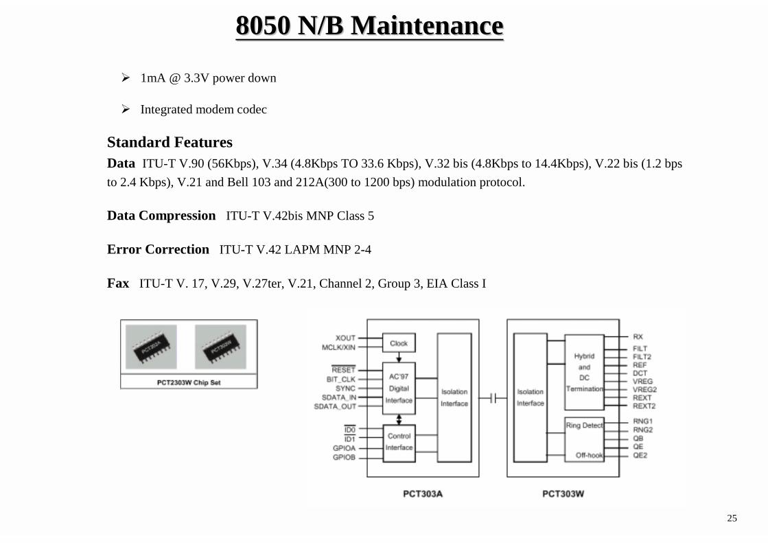
1.3.8 MDC:PCTEL MODEM DAUGHTER CARD PCT2303W (ASKEY V1456VQL-P1)
The PCT2303W chipset is designed to meet the demand of this emerging worldwide AMR/MDC market. TheofPC-TEL’s well proven PCT2303W chipset and the HSP56TM MR software modem driver allows systems manufactures to implement modem functions in PCs at a lower bill of materials (BOM) while maintaining higher system performance.
8050 8050 N/B MaintenanceN/B Maintenance
23
PC-TEL has streamlined the traditional modem into the Host Signal Processing (HSP) solution. Operating withthe Pentium class processors, HSP becomes part of the host computer’s system software. It requires less power to operate and less physical space than standard modem solutions. PC-TEL’s HSP modem is an easily integrated, cost-effective communications solution that is flexible enough to carry you into the future.
The PCT2303W chip set is an integrated direct access arrangement (DAA) and Codec that provides a programmable line interface to meet international telephone line requirements. The PCT2303W chip set is available in two 16-pin small outline packages (AC’97 interface on PCT303A and phone-line interface on PCT303W). The chip set eliminates the need for an AFE, an isolation transformer, relays, opto-isolators, and 2-to 4-wire hybrid. The PCT2303W chip set dramatically reduces the number of discrete components and cost required to achieve compliance with international regulatory requirements. The PCT2303W complies with AC’97 Interface specification Rev. 2.1.
The chip set is fully programmable to meet world-wide telephone line interface requirements including those described by CTR21, NET4, JATE, FCC, and various country-specific PTT specifications. The programmable parameters of the PCT2303W chip set include AC termination, DC termination, ringer impedance, and ringer threshold. The PCT2303W chip set has been designed to meet stringent world-wide requirements for out-of-band energy, billing-tone immunity, lightning surges, and safety requirements.
Features
Virtual com port with a DTE throughout up to 460.8Kbps.
G3 Fax compatible
8050 8050 N/B MaintenanceN/B Maintenance
24
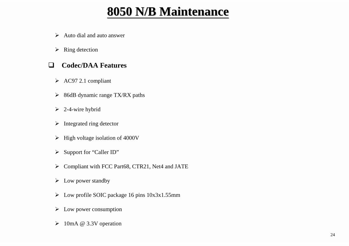
Codec/DAA Features
AC97 2.1 compliant
86dB dynamic range TX/RX paths
2-4-wire hybrid
Integrated ring detector
High voltage isolation of 4000V
Support for “Caller ID”
Compliant with FCC Part68, CTR21, Net4 and JATE
Low power standby
Low profile SOIC package 16 pins 10x3x1.55mm
Low power consumption
10mA @ 3.3V operation
Auto dial and auto answer
Ring detection
8050 8050 N/B MaintenanceN/B Maintenance
25
Standard FeaturesData ITU-T V.90 (56Kbps), V.34 (4.8Kbps TO 33.6 Kbps), V.32 bis (4.8Kbps to 14.4Kbps), V.22 bis (1.2 bps to 2.4 Kbps), V.21 and Bell 103 and 212A(300 to 1200 bps) modulation protocol.
Data Compression ITU-T V.42bis MNP Class 5
Error Correction ITU-T V.42 LAPM MNP 2-4
Fax ITU-T V. 17, V.29, V.27ter, V.21, Channel 2, Group 3, EIA Class I
1mA @ 3.3V power down
Integrated modem codec
8050 8050 N/B MaintenanceN/B Maintenance
26
1.3.9 IEEE1394 VT6307L (Option)
1.3.9.1 Overview
The VT6307 IEEE 1394 OHCI Host Controller provides high performance serial connectivity. It implements the Link and Phy layers for IEEE 1394-1995 High Performance Serial Bus specification release 1.0 and 1394a-2000. It is compliant with 1394 Open HCI 1.0 and 1.1 with DMA engine support for high performance data transfer via a 32-bit bus master PCI host bus interface. The VT6307 supports 100, 200 and 400 M bit/sec transmission via an integrated 2-port PHY. The VT6307 services two types of data packets: asynchronous and isochronous (real time). The 1394 link core performs arbitration requesting, packet generation and checking, and bus cycle master operations. It also has root node capability and performs retry operations. The VT6307 is ready to provide industry-standard IEEE 1394 peripheral connections for desktop and mobile PC platforms. Support for the VT6307 is built into Microsoft Windows 98, Windows ME, Windows 2000, and Windows XP.
32 bit CRC generator and checker for receive and transmit data
On-chip isochronous and asynchronous receive and transmit FIFOs for packets (2K for general receive plus 2K for isochronous transmit plus 2K for asynchronous transmit)
8 isochronous transmit contexts
4 isochronous receive contexts
1.3.9.2. Features
8050 8050 N/B MaintenanceN/B Maintenance
27
3-deep physical post-write queue
2-deep physical response queue
Dual buffer mode enhancements
Skip Processing enhancements
Block Read Request handling
Ack_tardy processing
Firmware Hub for Intel® 810, 810E, 815, 815E,815EP, 820, 840, 850 Chipsets
Flexible Erase Capability
1.3.10 System Flash Memory (BIOS)
Uniform 4 K Byte Sectors
Uniform 16 K Byte overlay blocks for SST49LF002A
Uniform 64 K Byte overlay blocks for SST49LF004ATop boot block protection
16 K Byte for SST49LF002A

8050 8050 N/B MaintenanceN/B Maintenance
28
5-signal communication interface supporting byte Read and Write
33 MHz clock frequency operation
WP# and TBL# pins provide hardware write protect for entire chip and/or top Boot Block
Block Locking Register for all blocks
Standard SDP Command Set
Data# Polling and Toggle Bit for End-of-Write detection
5 GPI pins for system design flexibility
4 ID pins for multi-chip selection
Single 3.0-3.6V Read and Write Operations
Superior Reliability
Firmware Hub Hardware Interface Mode
64 K Byte for SST49LF004A
Chip-Erase for PP Mode
8050 8050 N/B MaintenanceN/B Maintenance
29
JEDEC-standard 200-pin, small-outline, dual in-line memory module (SODIMM)
Utilizes 200 Mb/s and 266 Mb/s DDR SDRAM components
64MB (8 Meg x 64 [H]); 128MB (16 Meg x 64, [H] and [HD]); 256MB (32 Meg x 64 [HD]); 512MB (64Meg x 64 [HD])
VDD= VDDQ= +2.5V ±0.2V
VDDSPD = +2.2V to +5.5V
2.5V I/O (SSTL_2 compatible)
Commands entered on each positive CK edge
DQS edge-aligned with data for READs; center-aligned with data for WRITEs
Internal, pipelined double data rate (DDR) architecture; two data accesses per clock cycle Bidirectional data strobe (DQS) transmitted/received with data—i.e.,source-synchronous data capture
Differential clock inputs (CK and CK# - can be multiple clocks, CK0/CK0#, CK1/CK1#, etc.)
1.3.11 Memory System
1.3.11.1 64MB, 128MB, 256MB, 512MB (x64) 200-Pin DDR SDRAM SODIMM
8050 8050 N/B MaintenanceN/B Maintenance
30
Four internal device banks for concurrent operation
Selectable burst lengths: 2, 4, or 8
Auto precharge option
Auto Refresh and Self Refresh Modes
15.6µs (MT4VDDT864H, MT8VDDT1664HD), 7.8125µs (MT4VDDT1664H, MT8VDDT3264HD, MT8VDDT6464HD) maximum average periodic refresh interval
Serial Presence Detect (SPD) with EEPROM
Fast data transfer rates PC2100 or PC1600
Selectable READ CAS latency for maximum compatibility
Gold-plated edge contacts
1.3.12 PHY: 3.3-V 10Base-T/100Base-TX Integrated PHY Ceiver ,The ICS1893 is a low-power, physical-layer device (PHY)
General
The Realtek RTL8100C(L) is a highly integrated, cost-effective single-chip Fast Ethernet controller that provides 32-bit performance, PCI bus master capability, and full compliance with IEEE 802.3u 100Base-T specifications
8050 8050 N/B MaintenanceN/B Maintenance
31
and IEEE 802.3x Full Duplex Flow Control. It also supports the Advanced Configuration Power management Interface (ACPI), PCI power management for modern operating systems that are capable of Operating System Directed Power Management (OSPM) to achieve the most efficient power management possible.The RTL8100C(L) does not support CardBus mode as the RTL8139C does. In addition to the ACPI feature, theRTL8100C(L) also supports remote wake-up (including AMD Magic Packet, LinkChg, and Microsoft® wake-upframe) in both ACPI and APM environments. The RTL8100C(L) is capable of performing an internal resetthrough the application of auxiliary power. When auxiliary power is applied and the main power remains off, the RTL8100C(L) is ready and waiting for the Magic Packet or Link Change to wake the system up. Also, the LWAKE pin provides 4 different output signals including active high, active low, positive pulse, and negative pulse. The versatility of the RTL8100C(L) LWAKE pin provides motherboards with Wake-On-LAN (WOL) functionality. The RTL8100C(L) also supports Analog Auto-Power-down, that is, the analog part of the RTL8100C(L) can be shut down temporarily according to user requirements or when the RTL8100C(L) is in a power down state with the wakeup function disabled.In addition, when the analog part is shut down and the Isolate B pin is low (i.e. the main power is off), then both the analog and digital parts stop functioning and the power consumption of the RTL8100C(L) will be negligible. The RTL8100C(L) also supports an auxiliary power auto-detect function, and will auto-configure related bits of their own PCI power management registers in PCI configuration space.
128 pin QFP/LQFP
Integrated Fast Ethernet MAC, Physical chip and transceiver in one chip
10 Mb/s and 100 Mb/s operation
Supports 10 Mb/s and 100 Mb/s N-way Auto-negotiation operation

8050 8050 N/B MaintenanceN/B Maintenance
32
Compliant to PCI Revision 2.2Supports PCI clock 16.75MHz-40MHz
Supports PCI target fast back-to-back transaction
Provides PCI bus master data transfers and PCI
Memory space or I/O space mapped data transfers of RTL8100C(L)'s operational registers
Supports PCI VPD (Vital Product Data)
Supports ACPI, PCI power management
Supports 25MHz crystal or 25MHz OSC as the internal
Clock source. The frequency deviation of either crystal or OSC must be within 50 PPM.
Compliant to PC99/PC2001 standard
Supports Wake-On-LAN function and remote wake-up (Magic Packet*, LinkChg and Microsoft® wake-up frame)
Supports 4 Wake-On-LAN (WOL) signals (active high, active low, positive pulse, and negative pulse)
Supports auxiliary power-on internal reset, to be ready for remote wake-up when main power still remains off
PCI local bus single-chip Fast Ethernet controller
8050 8050 N/B MaintenanceN/B Maintenance
33
Supports auxiliary power auto-detect, and sets the related capability of power management registers in PCI configuration space.
Includes a programmable, PCI burst size and early Tx/Rx threshold. Supports a 32-bit general-purpose timer with the external PCI clock as clock source, to generate timer-interrupt
Contains two large (2Kbyte) independent receive and transmit FIFOs
Advanced power saving mode when LAN function or wakeup function is not used
Uses 93C46 (64*16-bit EEPROM) to store resource configuration, ID parameter, and VPD data.
Supports LED pins for various network activity indications
Supports loopback capability
Half/Full duplex capability
Supports Full Duplex Flow Control (IEEE 802.3x)
8050 8050 N/B MaintenanceN/B Maintenance
34
2.1 System View
2.1.1 Front View
Line Out Connector
1394 Jack
MIC In ConnectorLine In Connector
2.1.2 Left-side View
USB Ports *1
RJ-11 Connector
VGA Port
Ventilation Openings
S-Video Port
SD Card Slot
Top Cover Latch
RJ-45 ConnectorPCMCIA Card Socket
2. System View and Disassembly
8050 8050 N/B MaintenanceN/B Maintenance
35
2.1.3 Right-side View
2.1.4 Rear View
Kensington Lock
Power Connector
CD-ROM/DVD-ROM Drive
USB Port*2
Kensington Lock
8050 8050 N/B MaintenanceN/B Maintenance
36
2.1.5 Bottom View
Hard Disk DriveDDR SDRAM Card
Wireless Card
2.1.6 Top-open View
LCD Screen
Device LED IndicatorsKeyboard
Stereo Speaker Set
Power Button
Battery ParkCPU
Touch PadHard Disk Drive IndicatorBattery Power Charging Indicator
Stereo Speaker Set
Power Indicator
8050 8050 N/B MaintenanceN/B Maintenance
37
2.2 System Disassembly The section discusses at length each major component for disassembly/reassembly and show corresponding illustrations.Use the chart below to determine the disassembly sequence for removing components from the notebook.NOTE: Before you start to install/replace these modules, disconnect all peripheral devices and make sure the notebook is not turned on or connected to AC power.
Modular Components
LCD Assembly Components
Base Unit Components
NOTEBOOK
2.2.1 Battery Pack
2.2.2 Keyboard
2.2.3 CPU
2.2.4 HDD Module
2.2.5 DVD-ROM Drive
2.2.6 Wireless Card
2.2.7 Modem Card
2.2.8 DDR-SDRAM
2.2.9 LCD Assembly
2.2.10 LCD Panel
2.2.11 Inverter Board
2.2.12 System Board
2.2.13 Touch Pad
8050 8050 N/B MaintenanceN/B Maintenance
38
1. Replace the battery pack into the compartment. The battery pack should be correctly connected when youhear a clicking sound.
2. Slide the release lever to the “lock” ( ) position.
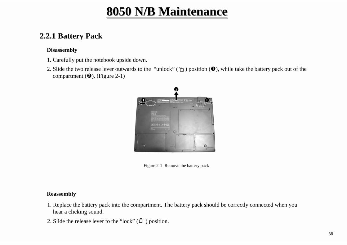
2.2.1 Battery Pack Disassembly
1. Carefully put the notebook upside down.2. Slide the two release lever outwards to the “unlock” ( ) position (), while take the battery pack out of the
compartment (). (Figure 2-1)
Figure 2-1 Remove the battery pack
Reassembly
8050 8050 N/B MaintenanceN/B Maintenance
39
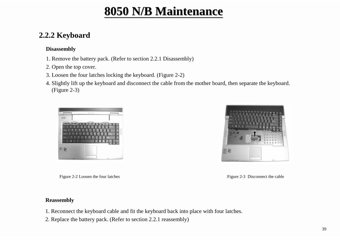
2.2.2 KeyboardDisassembly
1. Remove the battery pack. (Refer to section 2.2.1 Disassembly)2. Open the top cover.3. Loosen the four latches locking the keyboard. (Figure 2-2)4. Slightly lift up the keyboard and disconnect the cable from the mother board, then separate the keyboard.
(Figure 2-3)
Figure 2-2 Loosen the four latches Figure 2-3 Disconnect the cable
Reassembly
1. Reconnect the keyboard cable and fit the keyboard back into place with four latches. 2. Replace the battery pack. (Refer to section 2.2.1 reassembly)
8050 8050 N/B MaintenanceN/B Maintenance
40
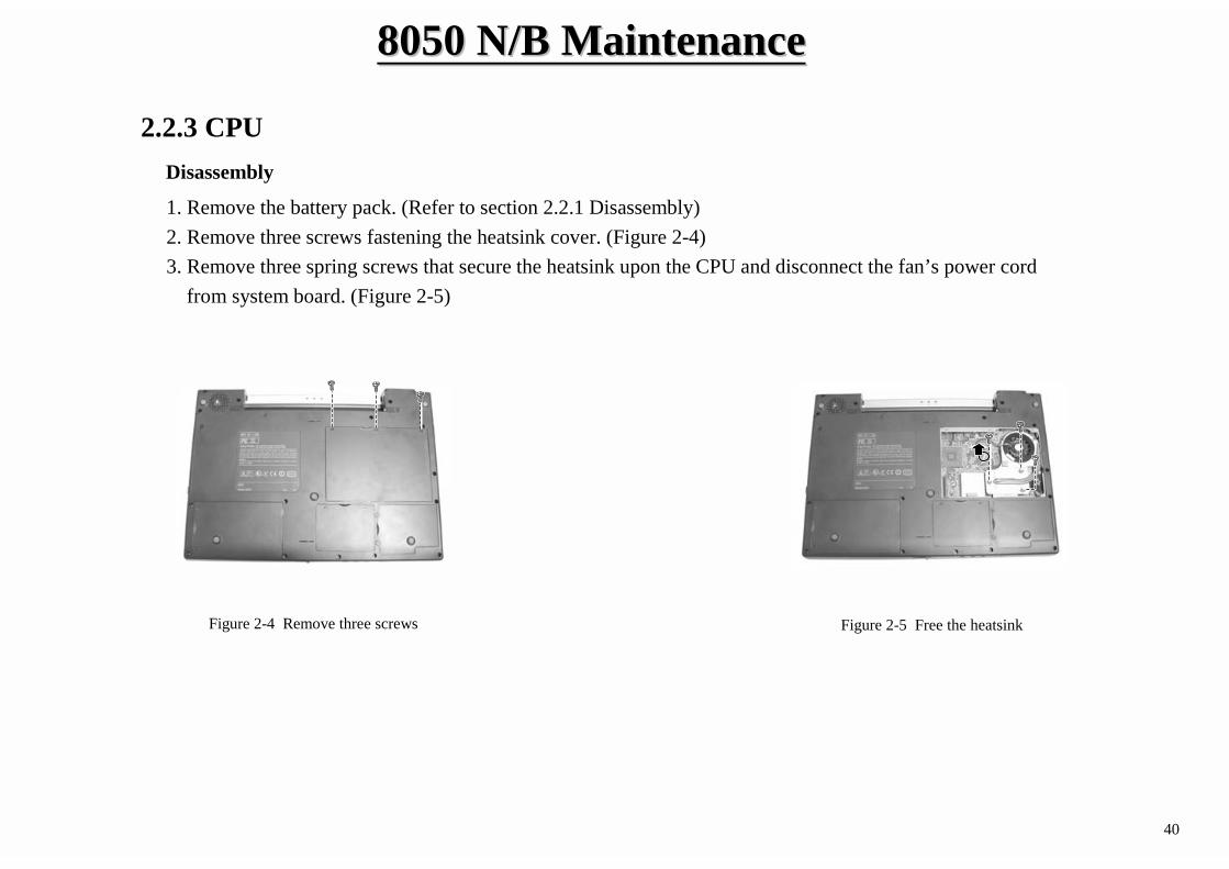
1. Remove the battery pack. (Refer to section 2.2.1 Disassembly)2. Remove three screws fastening the heatsink cover. (Figure 2-4)3. Remove three spring screws that secure the heatsink upon the CPU and disconnect the fan’s power cord
from system board. (Figure 2-5)
2.2.3 CPUDisassembly
Figure 2-4 Remove three screws Figure 2-5 Free the heatsink
8050 8050 N/B MaintenanceN/B Maintenance
41
Reassembly
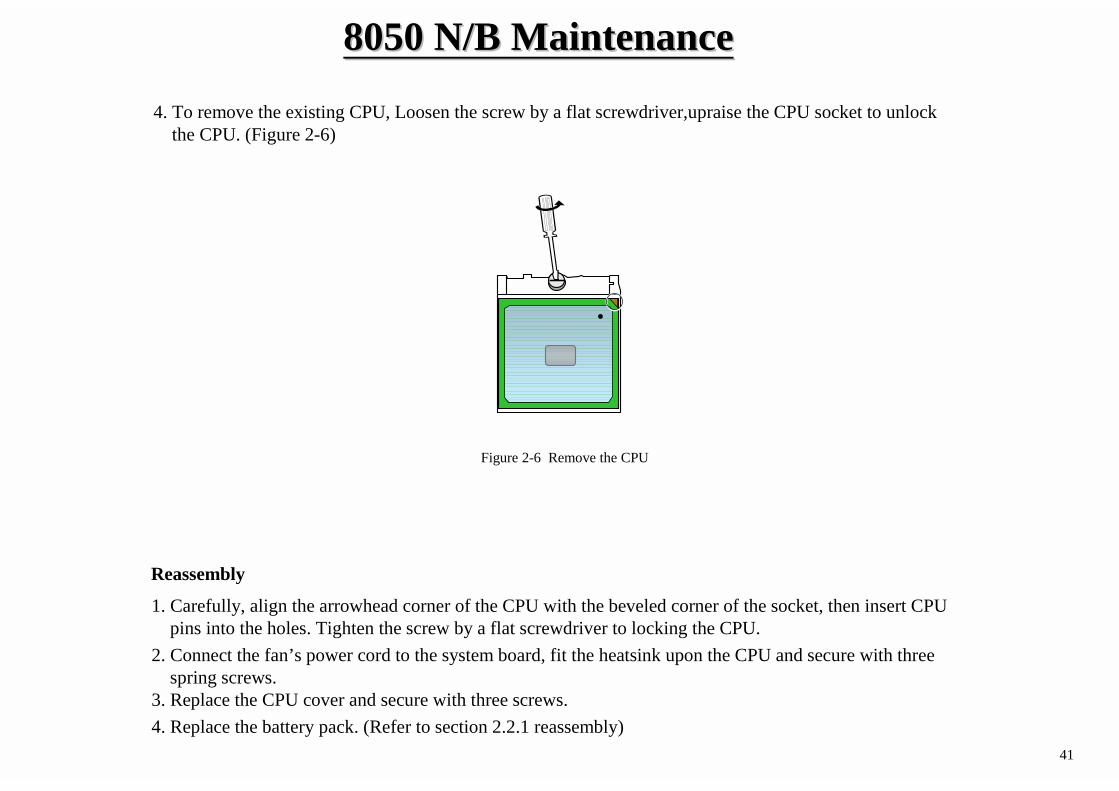
1. Carefully, align the arrowhead corner of the CPU with the beveled corner of the socket, then insert CPUpins into the holes. Tighten the screw by a flat screwdriver to locking the CPU.
2. Connect the fan’s power cord to the system board, fit the heatsink upon the CPU and secure with three spring screws.
3. Replace the CPU cover and secure with three screws.4. Replace the battery pack. (Refer to section 2.2.1 reassembly)
4. To remove the existing CPU, Loosen the screw by a flat screwdriver,upraise the CPU socket to unlock the CPU. (Figure 2-6)
Figure 2-6 Remove the CPU
8050 8050 N/B MaintenanceN/B Maintenance
42
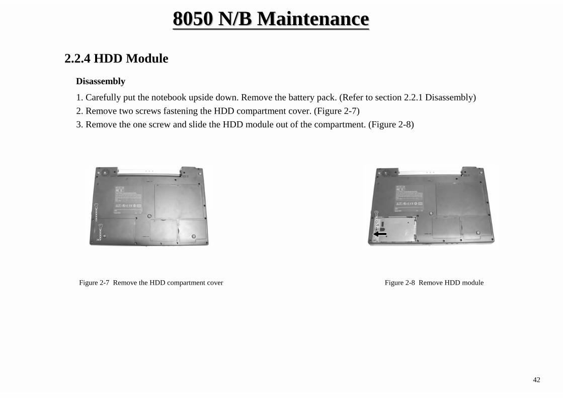
2.2.4 HDD Module Disassembly
1. Carefully put the notebook upside down. Remove the battery pack. (Refer to section 2.2.1 Disassembly)2. Remove two screws fastening the HDD compartment cover. (Figure 2-7)3. Remove the one screw and slide the HDD module out of the compartment. (Figure 2-8)
Figure 2-8 Remove HDD moduleFigure 2-7 Remove the HDD compartment cover
8050 8050 N/B MaintenanceN/B Maintenance
43
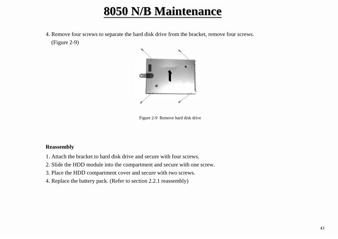
4. Remove four screws to separate the hard disk drive from the bracket, remove four screws. (Figure 2-9)
Reassembly
1. Attach the bracket to hard disk drive and secure with four screws.2. Slide the HDD module into the compartment and secure with one screw.3. Place the HDD compartment cover and secure with two screws.4. Replace the battery pack. (Refer to section 2.2.1 reassembly)
Figure 2-9 Remove hard disk drive
8050 8050 N/B MaintenanceN/B Maintenance
44
2.2.5 CD/DVD-ROM Drive Disassembly
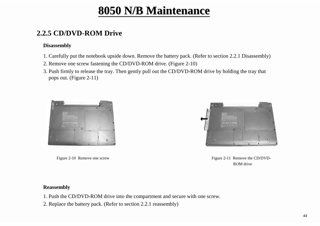
Figure 2-10 Remove one screw
1. Carefully put the notebook upside down. Remove the battery pack. (Refer to section 2.2.1 Disassembly)2. Remove one screw fastening the CD/DVD-ROM drive. (Figure 2-10)3. Push firmly to release the tray. Then gently pull out the CD/DVD-ROM drive by holding the tray that
pops out. (Figure 2-11)
Reassembly
1. Push the CD/DVD-ROM drive into the compartment and secure with one screw.2. Replace the battery pack. (Refer to section 2.2.1 reassembly)
Figure 2-11 Remove the CD/DVD-ROM drive
8050 8050 N/B MaintenanceN/B Maintenance
45
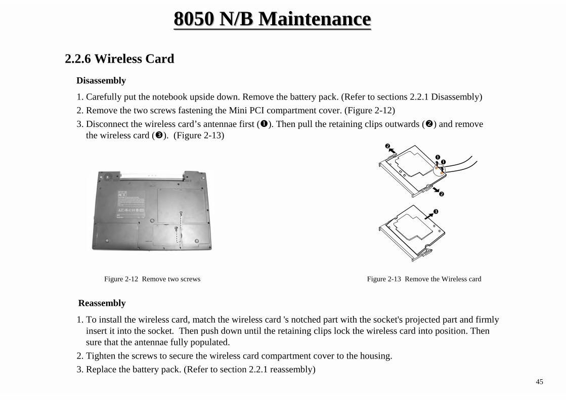
2.2.6 Wireless CardDisassembly
1. Carefully put the notebook upside down. Remove the battery pack. (Refer to sections 2.2.1 Disassembly)2. Remove the two screws fastening the Mini PCI compartment cover. (Figure 2-12)3. Disconnect the wireless card’s antennae first (). Then pull the retaining clips outwards () and remove
the wireless card (). (Figure 2-13)
Figure 2-12 Remove two screws
Figure 2-13 Remove the Wireless card
Reassembly
1. To install the wireless card, match the wireless card 's notched part with the socket's projected part and firmlyinsert it into the socket. Then push down until the retaining clips lock the wireless card into position. Thensure that the antennae fully populated.
2. Tighten the screws to secure the wireless card compartment cover to the housing. 3. Replace the battery pack. (Refer to section 2.2.1 reassembly)
8050 8050 N/B MaintenanceN/B Maintenance
46
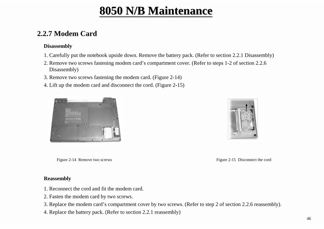
2.2.7 Modem CardDisassembly
1. Carefully put the notebook upside down. Remove the battery pack. (Refer to section 2.2.1 Disassembly)2. Remove two screws fastening modem card’s compartment cover. (Refer to steps 1-2 of section 2.2.6
Disassembly)3. Remove two screws fastening the modem card. (Figure 2-14)4. Lift up the modem card and disconnect the cord. (Figure 2-15)
Figure 2-14 Remove two screws Figure 2-15 Disconnect the cord
Reassembly
1. Reconnect the cord and fit the modem card.2. Fasten the modem card by two screws.3. Replace the modem card’s compartment cover by two screws. (Refer to step 2 of section 2.2.6 reassembly).4. Replace the battery pack. (Refer to section 2.2.1 reassembly)
8050 8050 N/B MaintenanceN/B Maintenance
47
2.2.8 DDR-SDRAM
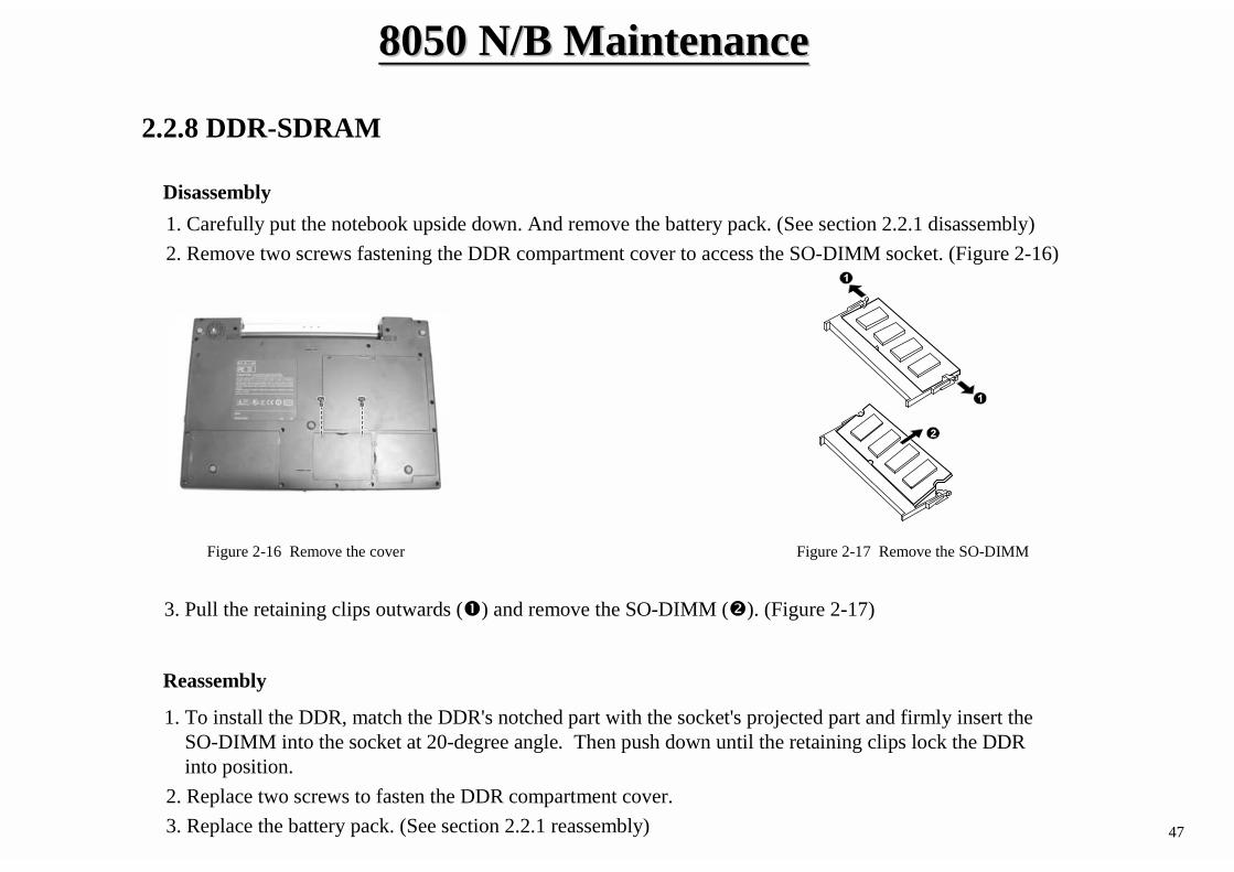
Disassembly 1. Carefully put the notebook upside down. And remove the battery pack. (See section 2.2.1 disassembly)2. Remove two screws fastening the DDR compartment cover to access the SO-DIMM socket. (Figure 2-16)
Figure 2-16 Remove the cover Figure 2-17 Remove the SO-DIMM
3. Pull the retaining clips outwards () and remove the SO-DIMM (). (Figure 2-17)
Reassembly
1. To install the DDR, match the DDR's notched part with the socket's projected part and firmly insert the SO-DIMM into the socket at 20-degree angle. Then push down until the retaining clips lock the DDRinto position.
2. Replace two screws to fasten the DDR compartment cover.3. Replace the battery pack. (See section 2.2.1 reassembly)
8050 8050 N/B MaintenanceN/B Maintenance
48
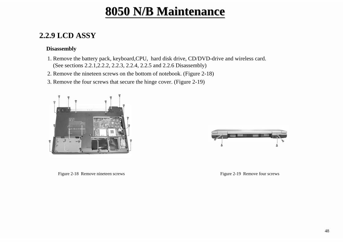
2.2.9 LCD ASSYDisassembly
1. Remove the battery pack, keyboard,CPU, hard disk drive, CD/DVD-drive and wireless card. (See sections 2.2.1,2.2.2, 2.2.3, 2.2.4, 2.2.5 and 2.2.6 Disassembly)
2. Remove the nineteen screws on the bottom of notebook. (Figure 2-18)3. Remove the four screws that secure the hinge cover. (Figure 2-19)
Figure 2-18 Remove nineteen screws Figure 2-19 Remove four screws
8050 8050 N/B MaintenanceN/B Maintenance
49
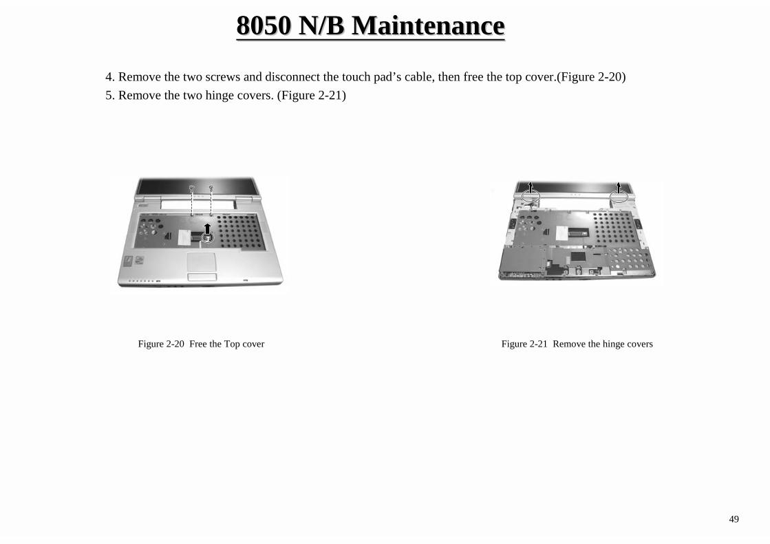
4. Remove the two screws and disconnect the touch pad’s cable, then free the top cover.(Figure 2-20) 5. Remove the two hinge covers. (Figure 2-21)
Figure 2-20 Free the Top cover Figure 2-21 Remove the hinge covers
8050 8050 N/B MaintenanceN/B Maintenance
50
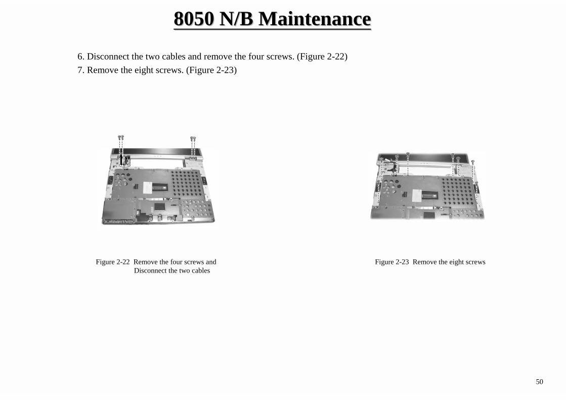
Figure 2-22 Remove the four screws andDisconnect the two cables
Figure 2-23 Remove the eight screws
6. Disconnect the two cables and remove the four screws. (Figure 2-22)7. Remove the eight screws. (Figure 2-23)
8050 8050 N/B MaintenanceN/B Maintenance
51
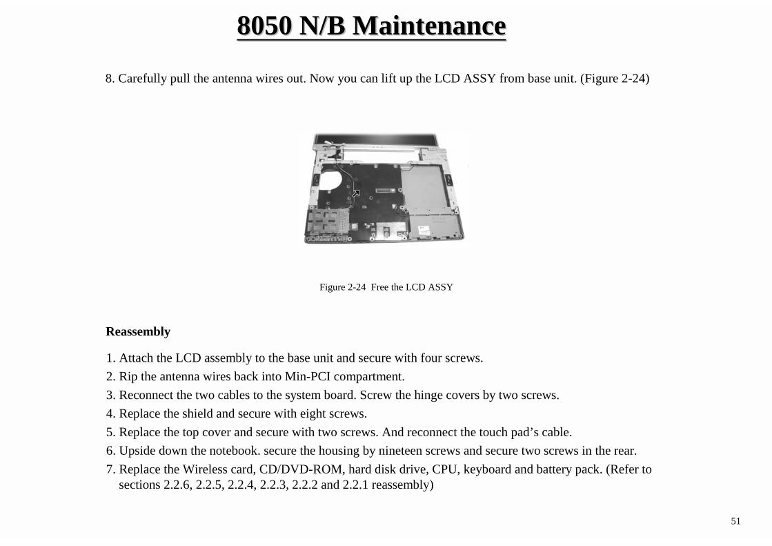
8. Carefully pull the antenna wires out. Now you can lift up the LCD ASSY from base unit. (Figure 2-24)
Figure 2-24 Free the LCD ASSY
1. Attach the LCD assembly to the base unit and secure with four screws. 2. Rip the antenna wires back into Min-PCI compartment.3. Reconnect the two cables to the system board. Screw the hinge covers by two screws.4. Replace the shield and secure with eight screws.5. Replace the top cover and secure with two screws. And reconnect the touch pad’s cable.6. Upside down the notebook. secure the housing by nineteen screws and secure two screws in the rear.7. Replace the Wireless card, CD/DVD-ROM, hard disk drive, CPU, keyboard and battery pack. (Refer to
sections 2.2.6, 2.2.5, 2.2.4, 2.2.3, 2.2.2 and 2.2.1 reassembly)
Reassembly
8050 8050 N/B MaintenanceN/B Maintenance
52
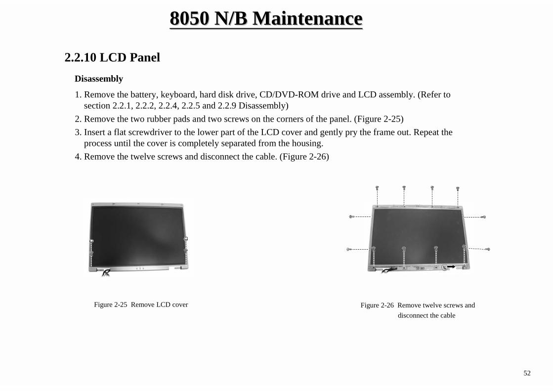
2.2.10 LCD PanelDisassembly
1. Remove the battery, keyboard, hard disk drive, CD/DVD-ROM drive and LCD assembly. (Refer to section 2.2.1, 2.2.2, 2.2.4, 2.2.5 and 2.2.9 Disassembly)
2. Remove the two rubber pads and two screws on the corners of the panel. (Figure 2-25)3. Insert a flat screwdriver to the lower part of the LCD cover and gently pry the frame out. Repeat the
process until the cover is completely separated from the housing.4. Remove the twelve screws and disconnect the cable. (Figure 2-26)
Figure 2-26 Remove twelve screws and disconnect the cable
Figure 2-25 Remove LCD cover
8050 8050 N/B MaintenanceN/B Maintenance
53
Reassembly
1. Replace the cable to the LCD.2. Attach the LCD panel’s bracket back to LCD panel and secure with six screws. 3. Replace the LCD panel into LCD housing.and reconnect two cables to inverter board and secure with two
screws.4. Fasten the LCD panel by ten screws.5. Fit the LCD cover and secure with two screws and rubber pads.6. Replace the LCD assembly, CD/DVD-ROM drive, hard disk drive, keyboard, battery pack. (See sections
2.2.9, 2.2.5, 2.2.4, 2.2.2, and 2.2.1 reassembly)
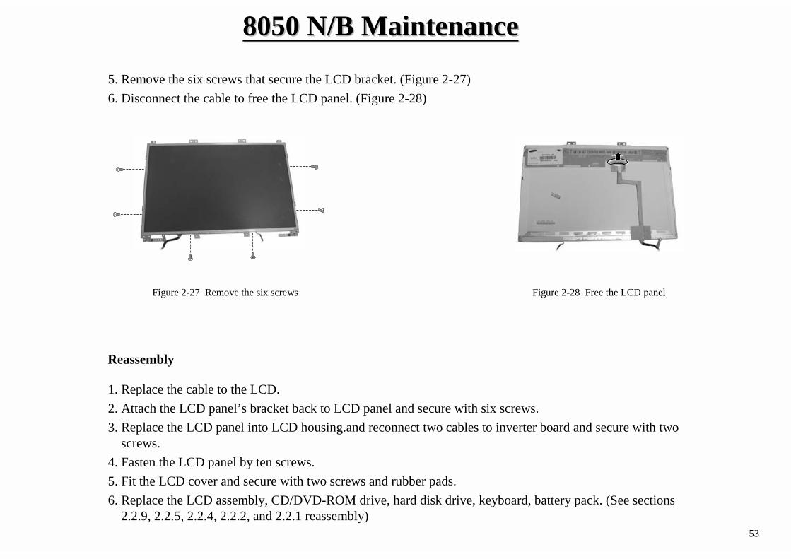
Figure 2-28 Free the LCD panel
5. Remove the six screws that secure the LCD bracket. (Figure 2-27)6. Disconnect the cable to free the LCD panel. (Figure 2-28)
Figure 2-27 Remove the six screws
8050 8050 N/B MaintenanceN/B Maintenance
54
2.2.11 Inverter BoardDisassembly
1. Remove the battery, keyboard, hard disk drive, CD/DVD-ROM drive and LCD assembly. (Refer to section 2.2.1, 2.2.2, 2.2.4, 2.2.5 and 2.2.9 Disassembly)
2. Remove the LCD cover and LCD panel. (Refer to the steps 1-4 of section 2.2.10 Disassembly )3. Remove the one screw fastening the inverter board and disconnect the cable, Then free the inverter board.
(Figure 2-29)
Figure 2-29 Free the inverter board
Reassembly1. Reconnect the cable. Fit the inverter board back into place and secure with one screw. 2. Replace the LCD Panel and LCD cover. (Refer to section 2.2.10 reassembly) 3. Replace the LCD assembly. (Refer to section 2.2.9 reassembly)4. Replace the CD/DVD-ROM drive, hard disk drive, keyboard and battery pack. (Refer to sections 2.2.5,
2.2.4, 2.2.2 and 2.2.1 reassembly)
8050 8050 N/B MaintenanceN/B Maintenance
55
1. Remove the battery, keyboard, hard disk drive, CD/DVD-ROM drive, Wireless card and LCD assembly. (Refer to sections 2.2.1, 2.2.2, 2.2.4, 2.2.5, 2.2.6 and 2.2.9 Disassembly)
2. Remove the four screws that secure the system board and disconnect the two speaker’s cables. Then lift itup from the housing. (Figure 2-30)
3. Disconnect the one speaker’s cables from the system board and remove the two screws, Then separate the bracket and free the system board. (Figure 2-31)
2.2.12 System BoardDisassembly
Figure 2-30 Remove four screws anddisconnect the two cables Figure 2-31 Free the system board
Reassembly
1. Fit the bracket and secure with two screws .2. Turn over the system board. Reconnect the speaker’s cords.3. Replace the system board back into the housing and secure with four screws, then reconnect the cable. 4. Replace the LCD assembly, CD/DVD-ROM, HDD, keyboard and battery pack. (Refer to previous section
reassembly)
8050 8050 N/B MaintenanceN/B Maintenance
56
2.2.13 Touch Pad Disassembly1. Remove the battery pack, keyboard, hard disk drive and CD/DVD-drive. (See sections 2.2.1,2.2.2 , 2.2.4 and
2.2.5 Disassembly)2. Remove the top cover. (See steps 1-5 in section 2.2.9 Disassembly) 3. Remove the two screws and free the touch pad. (Figure 2-32).
Reassembly
1. Replace the touch pad and secure the two screws.2. Replace the top cover. (Refer to the section in 2.2.9 reassembly)3. Replace the battery pack, keyboard, hard disk drive and CD/DVD-drive. (See sections 2.2.1,2.2.2 ,
2.2.4 and 2.2.5 Disassembly).
Figure 2-32 Remove the two screws
8050 8050 N/B MaintenanceN/B Maintenance
57
3. Definition & Location of Connectors / Switches
3.1 Mother Board - A
J1 : Inverter Board Connector
J2 : LCD panel connector
J3 : Internal Left Speaker Connector
J4 : Touch-pad Module Connector
J5 : Internal Key-board Connector
J6 : PCMCIA Card Connector
J7 : Internal Right Speaker Connector
SW2 : Power Button
SW4 : Left Button Switch of Touch-pad
SW5 : Right Button Switch of Touch-pad
J6
J2
J1
J3
J5
J4J7
SW4
SW5
SW2
8050 8050 N/B MaintenanceN/B Maintenance
58
3. Definition & Location of Connectors / Switches
3.2 Mother Board - B
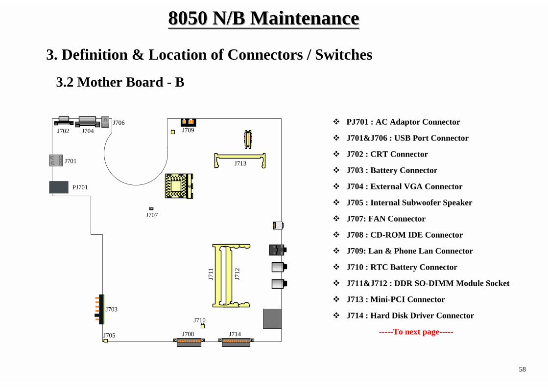
PJ701 : AC Adaptor Connector
J701&J706 : USB Port Connector
J702 : CRT Connector
J703 : Battery Connector
J704 : External VGA Connector
J705 : Internal Subwoofer Speaker
J707: FAN Connector
J708 : CD-ROM IDE Connector
J709: Lan & Phone Lan Connector
J710 : RTC Battery Connector
J711&J712 : DDR SO-DIMM Module Socket
J713 : Mini-PCI Connector
J714 : Hard Disk Driver Connector
-----To next page-----
J706
PJ701
J701 J713
J711
J712
J705
J703
J708 J714
J710
J702 J704
J707
J709
8050 8050 N/B MaintenanceN/B Maintenance
59
3. Definition & Location of Connectors / Switches
3.2 Mother Board - B
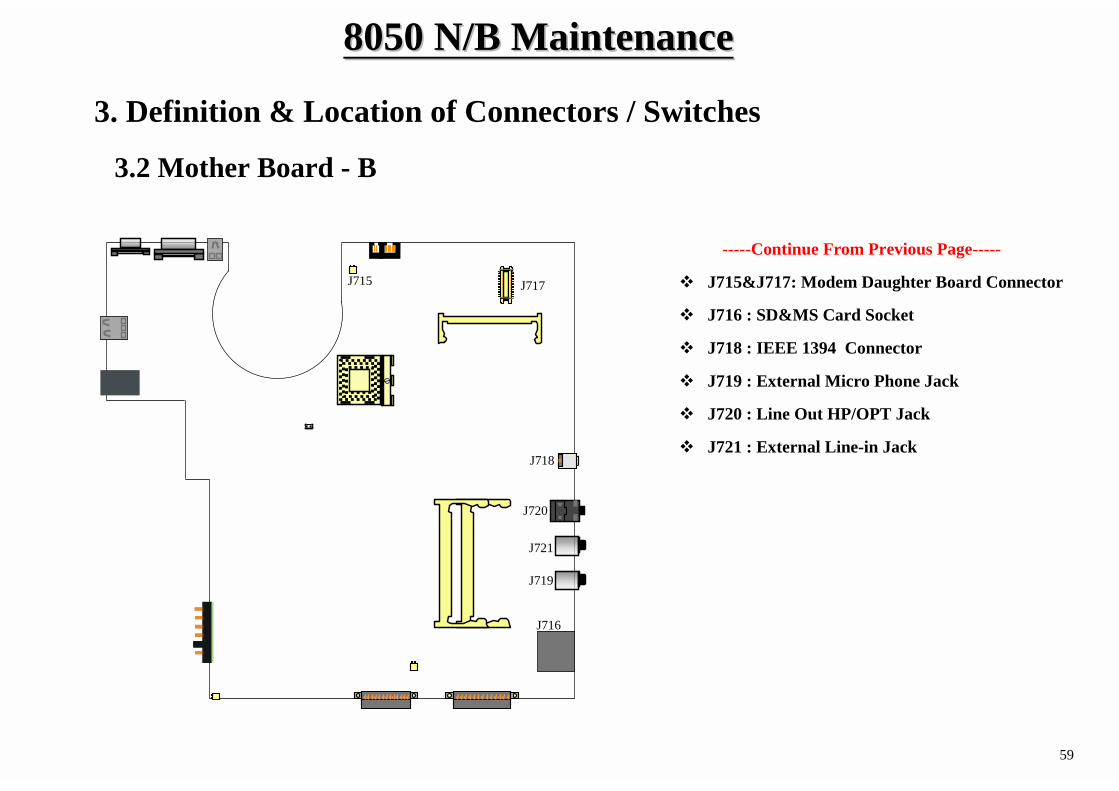
-----Continue From Previous Page-----
J715&J717: Modem Daughter Board Connector
J716 : SD&MS Card Socket
J718 : IEEE 1394 Connector
J719 : External Micro Phone Jack
J720 : Line Out HP/OPT Jack
J721 : External Line-in Jack
J719
J721
J720
J715 J717
J718
J716
8050 8050 N/B MaintenanceN/B Maintenance
60
4. Definition & Location of Major Components
4.1 Mother Board - A
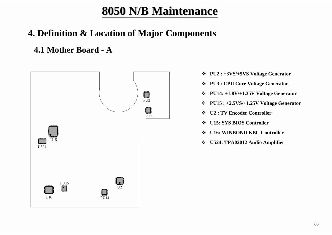
PU2 : +3VS/+5VS Voltage Generator
PU3 : CPU Core Voltage Generator
PU14: +1.8V/+1.35V Voltage Generator
PU15 : +2.5VS/+1.25V Voltage Generator
U2 : TV Encoder Controller
U15: SYS BIOS Controller
U16: WINBOND KBC Controller
U524: TPA02012 Audio Amplifier
PU2
PU3
U2
PU14
PU15
U16
U524
U15
8050 8050 N/B MaintenanceN/B Maintenance
61
4. Definition & Location of Major Components
4.2 Mother Board - B
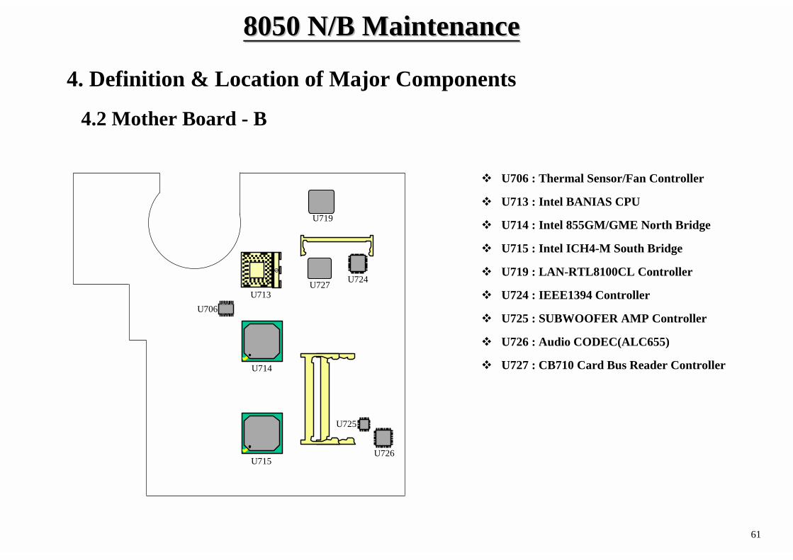
U706 : Thermal Sensor/Fan Controller
U713 : Intel BANIAS CPU
U714 : Intel 855GM/GME North Bridge
U715 : Intel ICH4-M South Bridge
U719 : LAN-RTL8100CL Controller
U724 : IEEE1394 Controller
U725 : SUBWOOFER AMP Controller
U726 : Audio CODEC(ALC655)
U727 : CB710 Card Bus Reader Controller
U715
U714
U713
U719
U727 U724
U706
U725
U726
8050 8050 N/B MaintenanceN/B Maintenance
62
5. Pin Descriptions of Major Components5.1 Intel Banias Pentium M Processor(1)
Signal Name Type Description A[31:3]#
I/O A[31:3]# (Address) define a 2 32 -byte physical memory address space. In sub-phase 1 of the address phase, these pins transmit the address of a transaction. In sub-phase 2, these pins transmit transaction type information. These signals must connect the appropriate pins of both agents on the Intel Pentium M processor system bus. A[31:3]# are source synchronous signals and are latched into the receiving buffers by ADSTB[1:0]#. Address signals are used as straps which are sampled before RESET# is deasserted.
A20M# I If A20M# (Address-20 Mask) is asserted, the processor masks physical address bit 20 (A20#) before looking up a line in any internal cache and before driving a read/write transaction on the bus. Asserting A20M# emulates the 8086 processor's address wrap-around at the 1-Mbyte boundary. Assertion of A20M# is only supported in real mode. A20M# is an asynchronous signal. However, to ensure recognition of this signal following an Input/Output write instruction, it must be valid along with the TRDY# assertion of the corresponding Input/Output Write bus transaction.
ADS# I/O ADS# (Address Strobe) is asserted to indicate the validity of the transaction address on the A[31:3]# and REQ[4:0]# pins. All bus agents observe the ADS# activation to begin parity checking, protocol checking, address decode, internal snoop, or deferred reply ID match operations associated with the new transaction.
ADSTB[1:0]# I/O Address strobes are used to latch A[31:3]# and REQ[4:0]# on their rising and falling edges. Strobes are associated with signals as shown below.
Signals Associated Strobe REQ[4:0]#, A[16:3]# ADSTB[0]# A[31:17]# ADSTB[1]#
BCLK[1:0] I The differential pair BCLK (Bus Clock) determines the system bus frequency. All processor system bus agents must receive these signals to drive their outputs and latch their inputs.
BNR# I/O BNR# (Block Next Request) is used to assert a bus stall by any bus agent that is unable to accept new bus transactions. During a bus stall, the current bus owner cannot issue any new transactions.
BPM[2:0]# BPM[3]
O I/O
BPM[3:0]# (Breakpoint Monitor) are breakpoint and performance monitor signals. They are outputs from the processor that indicate the status of breakpoints and programmable counters used for monitoring processor performance. BPM[3:0]# should connect the appropriate pins of all Intel Pentium M processor system bus agents. This includes debug or performance monitoring tools.
Signal Name Type Description BPRI# I BPRI# (Bus Priority Request) is used to arbitrate for ownership of the
processor system bus. It must connect the appropriate pins of both processor system bus agents. Observing BPRI# active (as asserted by the priority agent) causes the other agent to stop issuing new requests, unless such requests are part of an ongoing locked operation. The priority agent keeps BPRI# asserted until all of its requests are completed, then releases the bus by deasserting BPRI#.
BR0# I/O BR0# is used by the processor to request the bus. The arbitration is done between the Intel Pentium M processor (Symmetric Agent) and the MCH-M (High Priority Agent) of the Intel 855PM or Intel 855GM chipset.
COMPP3:0] Analog COMP[3:0] must be terminated on the system board using precision (1% tolerance) resistors. Refer to the platform design guides for more implementation details.
D[63:0]# I/O D[63:0]# (Data) are the data signals. These signals provide a 64-bit data path between the processor system bus agents, and must connect the appropriate pins on both agents. The data driver asserts DRDY# to indicate a valid data transfer. D[63:0]# are quad-pumped signals and will thus be driven four times in a common clock period. D[63:0]# are latched off the falling edge of both DSTBP[3:0]# and DSTBN[3:0]#. Each group of 16 data signals correspond to a pair of one DSTBP# and one DSTBN#. The following table shows the grouping of data signals to data strobes and DINV#. Quad-Pumped Signal Groups
Data Group DSTBN#/DSTBP# DINV#D[15:0]# 0 0 D[31:16]# 1 1 D[47:32]# 2 2 D[63:48]# 3 3
Furthermore, the DINV# pins determine the polarity of the data signals. Each group of 16 data signals corresponds to one DINV# signal. When the DINV# signal is active, the corresponding data group is inverted and therefore sampled active high.
DBR# O DBR# (Data Bus Reset) is used only in processor systems where no debug port is implemented on the system board. DBR# is used by a debug port interposer so that an in-target probe can drive system reset. If a debug port is implemented in the system, DBR# is a no connect. DBR# is not a processor signal.
8050 8050 N/B MaintenanceN/B Maintenance
63
5.1 Intel Banias Pentium M Processor(2)Signal Name Type Description
DBSY# I/O DBSY# (Data Bus Busy) is asserted by the agent responsible for driving data on the processor system bus to indicate that the data bus is in use. The data bus is released after DBSY# is deasserted. This signal must connect the appropriate pins on both processor system bus agents.
DEFER# I DEFER# is asserted by an agent to indicate that a transaction cannot beguaranteed in-order completion. Assertion of DEFER# is normally theresponsibility of the addressed memory or Input/Output agent. This signal must connect the appropriate pins of both processor system bus agents.
DINV[3:0]#
I/O DINV[3:0]# (Data Bus Inversion) are source synchronous and indicate the polarity of the D[63:0]# signals. The DINV[3:0]# signals are activated when the data on the data bus is inverted. The bus agent will invert the data bus signals if more than half the bits, within the covered group, would change level in the next cycle. DINV[3:0]# Assignment To Data Bus
Bus Signal Data Bus Signals DINV[3]# D[63:48]# DINV[2]# D[47:32]# DINV[1]# D[31:16]# DINV[0]# D[15:0]#
DPSLP# I DPSLP# when asserted on the platform causes the processor to transition from the Sleep state to the Deep Sleep state. In order to return to the Sleep state, DPSLP# must be deasserted. DPSLP# is driven by the ICH4-M component and also connects to the MCH-M component of the Intel 855PM or Intel 855GM chipset.
DRDY# I/O DRDY# (Data Ready) is asserted by the data driver on each data transfer, indicating valid data on the data bus. In a multi-common clock data transfer, DRDY# may be deasserted to insert idle clocks. This signal must connect the appropriate pins of both processor system bus agents.
DSTBN[3:0]# I/O Data strobe used to latch in D[63:0]#. Signals Associated Strobe D[15:0]#, DINV[0]# DSTBN[0]# D[31:16]#, DINV[1]# DSTBN[1]# D[47:32]#, DINV[2]# DSTBN[2]# D[63:48]#, DINV[3]# DSTBN[3]#
DSTBP[3:0]# I/O Data strobe used to latch in D[63:0]#. Signals Associated Strobe D[15:0]#, DINV[0]# DSTBP[0]# D[31:16]#, DINV[1]# DSTBP[1]# D[47:32]#, DINV[2]# DSTBP[2]# D[63:48]#, DINV[3]# DSTBP[3]#
Signal Name Type Description DPWR# I DPWR# is a control signal from the Intel 855PM and Intel 855GM
chipsets used to reduce power on the Intel Pentium M data bus input buffers.
FERR#/PBE# O FERR# (Floating-point Error)/PBE#(Pending Break Event) is a multiplexed signal and its meaning is qualified by STPCLK#. When STPCLK# is not asserted, FERR#/PBE# indicates a floating point when the processor detects an unmasked floating-point error. FERR# is similar to the ERROR# signal on the Intel 80387 coprocessor, and is included for compatibility with systems using MS-DOS* type floating-point error reporting. When STPCLK# is asserted, an assertion of FERR#/PBE# indicates that the processor has a pending break event waiting for service. The assertion of FERR#/PBE# indicates that the processor should be returned to the Normal state. When FERR#/PBE# is asserted, indicating a break event, it will remain asserted until STPCLK# is deasserted. Assertion of PREQ# when STPCLK# is active will also cause an FERR# break event.
GTLREF I GTLREF determines the signal reference level for AGTL+ input pins. GTLREF should be set at 2/3 VCCP . GTLREF is used by the AGTL+ receivers to determine if a signal is a logical 0 or logical 1.
HIT# HITM#
I/O I/O
HIT# (Snoop Hit) and HITM# (Hit Modified) convey transaction snoop operation results. Either system bus agent may assert both HIT# and HITM# together to indicate that it requires a snoop stall, which can be continued by reasserting HIT# and HITM# together.
IERR# O IERR# (Internal Error) is asserted by a processor as the result of an internal error. Assertion of IERR# is usually accompanied by a SHUTDOWN transaction on the processor system bus. This transaction may optionally be converted to an external error signal (e.g., NMI) by system core logic. The processor will keep IERR# asserted until the assertion of RESET#, BINIT#, or INIT#.
IGNNE# I IGNNE# (Ignore Numeric Error) is asserted to force the processor to ignore a numeric error and continue to execute noncontrol floating-point instructions. If IGNNE# is deasserted, the processor generates an exception on a noncontrol floating-point instruction if a previous floating-point instruction caused an error. IGNNE# has no effect when the NE bit in control register 0 (CR0) is set. IGNNE# is an asynchronous signal. However, to ensure recognition of this signal following an Input/Output write instruction, it must be valid along with the TRDY# assertion of the corresponding Input/Output Write bus transaction.
REQ[4:0]# I/O REQ[4:0]# (Request Command) must connect the appropriate pins of both processor system bus agents. They are asserted by the current bus owner to define the currently active transaction type. These signals are source synchronous to ADSTB[0]#.
8050 8050 N/B MaintenanceN/B Maintenance
64
Signal Name Type Description INIT#
I INIT# (Initialization), when asserted, resets integer registers inside the processor without affecting its internal caches or floating-point registers. The processor then begins execution at the power on Reset vector configured during power on configuration. The processor continues to handle snoop requests during INIT# assertion. INIT# is an asynchronous signal. However, to ensure recognition of this signal following an Input/Output Write instruction, it must be valid along with the TRDY# assertion of the corresponding Input/Output Write bus transaction. INIT# must connect the appropriate pins of both processor system bus agents. If INIT# is sampled active on the active to inactive transition of RESET#, then the processor executes its Built-in Self-Test (BIST)
LINT[1:0] I LINT[1:0] (Local APIC Interrupt) must connect the appropriate pins of all APIC Bus agents. When the APIC is disabled, the LINT0 signal becomes INTR, a maskable interrupt request signal, and LINT1 becomes NMI, a nonmaskable interrupt. INTR and NMI are backward compatible with the signals of those names on the Pentium processor. Both signals are asynchronous. Both of these signals must be software configured using BIOS programming of the APIC register space and used either as NMI/INTR or LINT[1:0]. Because the APIC is enabled by default after Reset, operation of these pins as LINT[1:0] is the default configuration.
LOCK# I/O LOCK# indicates to the system that a transaction must occur atomically. This signal must connect the appropriate pins of both processor system bus agents. For a locked sequence of transactions, LOCK# is asserted from the beginning of the first transaction to the end of the last transaction. When the priority agent asserts BPRI# to arbitrate for ownership of theprocessor system bus, it will wait until it observes LOCK# deasserted. This enables symmetric agents to retain ownership of the processor system bus throughout the bus locked operation and ensure the atomicity of lock.
PRDY#
O Probe Ready signal used by debug tools to determine processor debug readiness.
PREQ# I Probe Request signal used by debug tools to request debug operation of the processor.
PROCHOT# O PROCHOT# (Processor Hot) will go active when the processor temperature monitoring sensor detects that the processor has reached its maximum safe operating temperature. This indicates that the processor Thermal Control Circuit has been activated, if enabled. This signal may require voltage translation on the motherboard.
PSI# O Processor Power Status Indicator signal. This signal is asserted when theprocessor is in a lower state (Deep Sleep and Deeper Sleep).
Signal Name Type Description PWRGOOD I PWRGOOD (Power Good) is a processor input. The processor requires
this signal as a clean indication that the clocks and power supplies are stable and within their specifications. ‘Clean’ implies that the signal will remain low (capable of sinking leakage current), without glitches, from the time that the power supplies are turned on until they come within specification. The signal must then transition monotonically to a high state. PWRGOOD can be driven inactive at any time, but clocks and power must again be stable before a subsequent rising edge of PWRGOOD. The PWRGOOD signal must be supplied to the processor; it is used to protect internal circuits against voltage sequencing issues. It should be driven high throughout the boundary scan operation.
ITP_CLK[1:0] I ITP_CLK[1:0] are copies of BCLK that are used only in processor systems where no debug port is implemented on the system board. ITP_CLK[1:0] are used as BCLK[1:0] references for a debug port implemented on an interposer. If a debug port is implemented in the system, ITP_CLK[1:0] are no connects. These are not processor signals.
RESET# I Asserting the RESET# signal resets the processor to a known state and invalidates its internal caches without writing back any of their contents. For a power-on Reset, RESET# must stay active for at least two milliseconds after VCC and BCLK have reached their proper specifications. On observing active RESET#, both system bus agents will deassert their outputs within two clocks. All processor straps must be valid within the specified setup time before RESET# is deasserted.
RS[2:0]# I RS[2:0]# (Response Status) are driven by the response agent (the agent responsible for completion of the current transaction), and must connect the appropriate pins of both processor system bus agents.
RSVD - These pins are RESERVED and must be left unconnected on the board. However, it is recommended that routing channels to these pins on the board be kept open for possible future use. Please refer to the platform design guides for more details.
SLP# I SLP# (Sleep), when asserted in Stop-Grant state, causes the processor to enter the Sleep state. During Sleep state, the processor stops providing internal clock signals to all units, leaving only the Phase-Locked Loop (PLL) still operating. Processors in this state will not recognize snoops or interrupts. The processor will recognize only assertion of the RESET# signal, deassertion of SLP#, and removal of the BCLK input while in Sleep state. If SLP# is deasserted, the processor exits Sleep state and returns to Stop-Grant state, restarting its internal clock signals to the bus and processor core units. If DPSLP# is asserted while in the Sleep state, the processor will exit the Sleep state and transition to the Deep Sleep state.
5.1 Intel Banias Pentium M Processor(3)
8050 8050 N/B MaintenanceN/B Maintenance
65
Signal Name Type Description SMI# I SMI# (System Management Interrupt) is asserted asynchronously by
system logic. On accepting a System Management Interrupt, the processor saves the current state and enter System Management Mode (SMM). An SMI Acknowledge transaction is issued, and the processor begins program execution from the SMM handler. If SMI# is asserted during the deassertion of RESET# the processor will tristate its outputs.
STPCLK# I STPCLK# (Stop Clock), when asserted, causes the processor to enter a low power Stop-Grant state. The processor issues a Stop-Grant Acknowledge transaction, and stops providing internal clock signals to all processor core units except the system bus and APIC units. The processor continues to snoop bus transactions and service interrupts while in Stop-Grant state. When STPCLK# is deasserted, the processor restarts its internal clock to all units and resumes execution. The assertion of STPCLK# has no effect on the bus clock; STPCLK# is an asynchronous input.
TCK I TCK (Test Clock) provides the clock input for the processor Test Bus (also known as the Test Access Port).
TDI I TDI (Test Data In) transfers serial test data into the processor. TDI provides the serial input needed for JTAG specification support.
TDO O TDO (Test Data Out) transfers serial test data out of the processor. TDOprovides the serial output needed for JTAG specification support.
TEST1, TEST2, TEST3
I TEST1, TEST2, and TEST3 must be left unconnected but should have a stuffing option connection to V SS separately using 1-k, pull-down resisitors.
THERMDA Other Thermal Diode Anode. THERMDC Other Thermal Diode Cathode. THERMTRIP# O The processor protects itself from catastrophic overheating by use of an
internal thermal sensor. This sensor is set well above the normal operating temperature to ensure that there are no false trips. The processor will stop all execution when the junction temperature exceeds approximately 125°C. This is signalled to the system by the THERMTRIP# (Thermal Trip) pin.
TMS I TMS (Test Mode Select) is a JTAG specification support signal used by debug tools.
TRDY# I TRDY# (Target Ready) is asserted by the target to indicate that it is ready to receive a write or implicit writeback data transfer. TRDY# must connect the appropriate pins of both system bus agents.
TRST# I TRST# (Test Reset) resets the Test Access Port (TAP) logic. TRST# must be driven low during power on Reset.
Signal Name Type Description VCC I Processor core power supply. VCCA[3:0] I VCCA provides isolated power for the internal processor core PLL’s. VCCP I Processor I/O Power Supply. VCCQ[1:0] I Quiet power supply for on die COMP circuitry. These pins should be
connected to VCCP on the motherboard. However, these connections should enable addition of decoupling on the VCCQ lines if necessary.
VCCSENSE O VCCSENSE is an isolated low impedance connection to processor core power (VCC ). It can be used to sense or measure power near the silicon with little noise.
VID[5:0] O VID[5:0] (Voltage ID) pins are used to support automatic selection of power supply voltages (Vcc). Unlike some previous generations of processors, these are CMOS signals that are driven by the Intel Pentium M processor. The voltage supply for these pins must be valid before the VR can supply Vcc to the processor. Conversely, the VR output must be disabled until the voltage supply for the VID pins becomes valid. The VID pins are needed to support the processor voltage specification variations.
VSSSENSE O VSSSENSE is an isolated low impedance connection to processor core VSS. It can be used to sense or measure ground near the silicon with little noise.
5.1 Intel Banias Pentium M Processor(4)
8050 8050 N/B MaintenanceN/B Maintenance
66
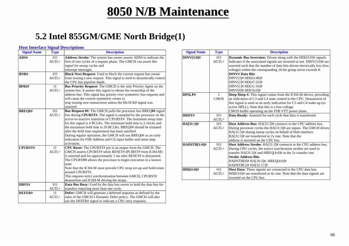
Host Interface Signal Descriptions Signal Name Type Description
ADS# I/O AGTL+
Address Strobe: The system bus owner asserts ADS# to indicate the first of two cycles of a request phase. The GMCH can assert this signal for snoop cycles and interrupt messages.
BNR# I/O AGTL+
Block Next Request: Used to block the current request bus owner from issuing a new request. This signal is used to dynamically control the CPU bus pipeline depth.
BPRI# O AGTL+
Bus Priority Request: The GMCH is the only Priority Agent on the system bus. It asserts this signal to obtain the ownership of the address bus. This signal has priority over symmetric bus requests and will cause the current symmetric owner to stop issuing new transactions unless the HLOCK# signal was asserted.
BREQ0# I/O AGTL+
Bus Request 0#: The GMCH pulls the processor bus BREQ0# signal low during CPURST#. The signal is sampled by the processor on the active-to-inactive transition of CPURST#. The minimum setup time for this signal is 4 BCLKs. The minimum hold time is 2 clocks and the maximum hold time is 20 BCLKs. BREQ0# should be tristated after the hold time requirement has been satisfied. During regular operation, the GMCH will use BREQ0# as an early indication for FSB Address and Ctl input buffer and sense amp activation.
CPURST# O AGTL+
CPU Reset: The CPURST# pin is an output from the GMCH. The GMCH asserts CPURST# while RESET# (PCIRST# from ICH4-M) is asserted and for approximately 1 ms after RESET# is deasserted. The CPURST# allows the processor to begin execution in a known state. Note that the ICH4-M must provide CPU strap set-up and hold-times around CPURST#. This requires strict synchronization between GMCH, CPURST# deassertion and ICH4-M driving the straps.
DBSY# I/O AGTL+
Data Bus Busy: Used by the data bus owner to hold the data bus for transfers requiring more than one cycle.
DEFER# O AGTL+
Defer: GMCH will generate a deferred response as defined by the rules of the GMCH’s Dynamic Defer policy. The GMCH will also use the DEFER# signal to indicate a CPU retry response.
Signal Name Type Description DINV[3:0]# I/O
AGTL+Dynamic Bus Inversion: Driven along with the HD[63:0]# signals. Indicates if the associated signals are inverted or not. DINV[3:0]# are asserted such that the number of data bits driven electrically low (low voltage) within the corresponding 16-bit group never exceeds 8. DINV# Data Bits DINV[3]# HD[63:48]# DINV[2]# HD[47:32]# DINV[1]# HD[31:16]# DINV[0]# HD[16:0]#
DPSLP# I CMOS
Deep Sleep #: This signal comes from the ICH4-M device, providing an indication of C3 and C4 state control to the CPU. Deassertion of this signal is used as an early indication for C3 and C4 wake up (to active HPLL). Note that this is a low-voltage CMOS buffer operating on the FSB VTT power plane.
DRDY# I/O AGTL+
Data Ready: Asserted for each cycle that data is transferred.
HA[31:3]# I/O AGTL+
Host Address Bus: HA[31:3]# connects to the CPU address bus. During processor cycles the HA[31:3]# are inputs. The GMCH drives HA[31:3]# during snoop cycles on behalf of Hub interface. HA[31:3]# are transferred at 2x rate. Note that the address is inverted on the CPU bus.
HADSTB[1:0]# I/O AGTL+
Host Address Strobe: HA[31:3]# connects to the CPU address bus. During CPU cycles, the source synchronous strobes are used to transfer HA[31:3]# and HREQ[4:0]# at the 2x transfer rate. Strobe Address Bits HADSTB[0]# HA[16:3]#, HREQ[4:0]# HADSTB[1]# HA[31:17]#
HD[63:0]# I/O AGTL+
Host Data: These signals are connected to the CPU data bus. HD[63:0]# are transferred at 4x rate. Note that the data signals are inverted on the CPU bus.
5.2 Intel 855GM/GME North Bridge(1)
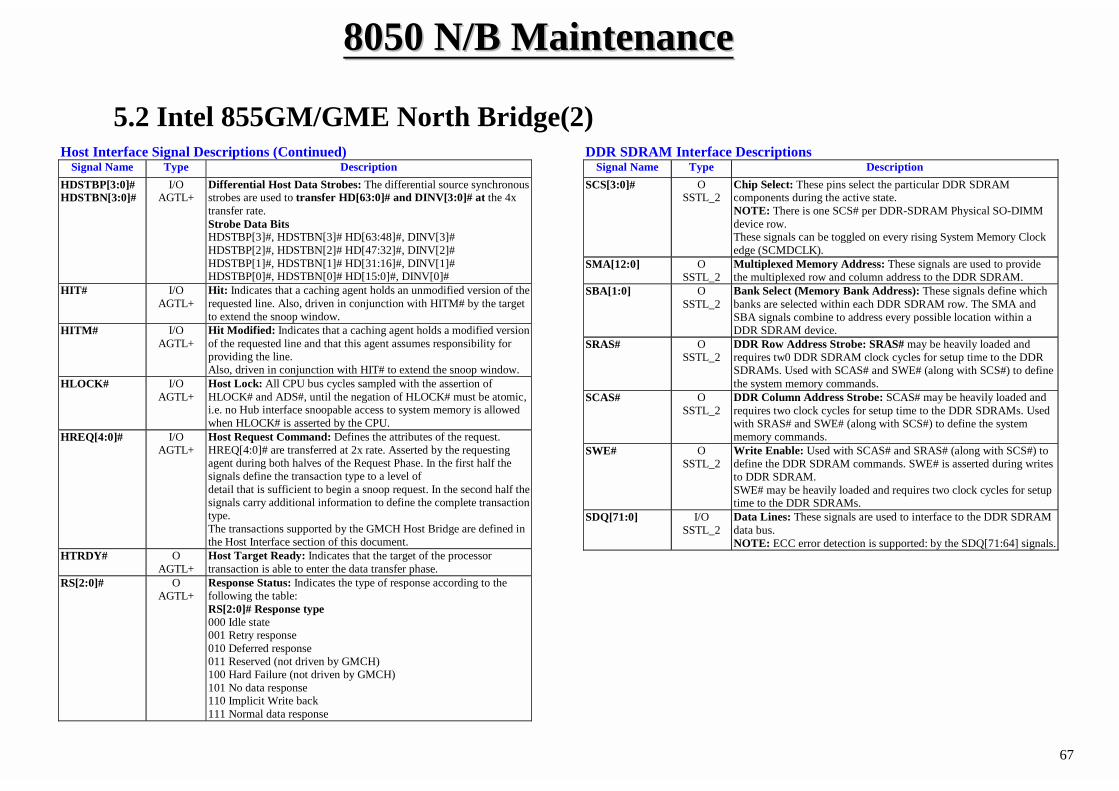
8050 8050 N/B MaintenanceN/B Maintenance
67
Host Interface Signal Descriptions (Continued) Signal Name Type Description
HDSTBP[3:0]# HDSTBN[3:0]#
I/O AGTL+
Differential Host Data Strobes: The differential source synchronous strobes are used to transfer HD[63:0]# and DINV[3:0]# at the 4x transfer rate. Strobe Data Bits HDSTBP[3]#, HDSTBN[3]# HD[63:48]#, DINV[3]# HDSTBP[2]#, HDSTBN[2]# HD[47:32]#, DINV[2]# HDSTBP[1]#, HDSTBN[1]# HD[31:16]#, DINV[1]# HDSTBP[0]#, HDSTBN[0]# HD[15:0]#, DINV[0]#
HIT# I/O AGTL+
Hit: Indicates that a caching agent holds an unmodified version of the requested line. Also, driven in conjunction with HITM# by the target to extend the snoop window.
HITM# I/O AGTL+
Hit Modified: Indicates that a caching agent holds a modified version of the requested line and that this agent assumes responsibility for providing the line. Also, driven in conjunction with HIT# to extend the snoop window.
HLOCK# I/O AGTL+
Host Lock: All CPU bus cycles sampled with the assertion of HLOCK# and ADS#, until the negation of HLOCK# must be atomic, i.e. no Hub interface snoopable access to system memory is allowed when HLOCK# is asserted by the CPU.
HREQ[4:0]# I/O AGTL+
Host Request Command: Defines the attributes of the request. HREQ[4:0]# are transferred at 2x rate. Asserted by the requesting agent during both halves of the Request Phase. In the first half the signals define the transaction type to a level of detail that is sufficient to begin a snoop request. In the second half the signals carry additional information to define the complete transactiontype. The transactions supported by the GMCH Host Bridge are defined in the Host Interface section of this document.
HTRDY# O AGTL+
Host Target Ready: Indicates that the target of the processor transaction is able to enter the data transfer phase.
RS[2:0]# O AGTL+
Response Status: Indicates the type of response according to the following the table: RS[2:0]# Response type 000 Idle state 001 Retry response 010 Deferred response 011 Reserved (not driven by GMCH) 100 Hard Failure (not driven by GMCH) 101 No data response 110 Implicit Write back 111 Normal data response
DDR SDRAM Interface Descriptions Signal Name Type Description
SCS[3:0]# O SSTL_2
Chip Select: These pins select the particular DDR SDRAM components during the active state. NOTE: There is one SCS# per DDR-SDRAM Physical SO-DIMM device row. These signals can be toggled on every rising System Memory Clock edge (SCMDCLK).
SMA[12:0] O SSTL_2
Multiplexed Memory Address: These signals are used to provide the multiplexed row and column address to the DDR SDRAM.
SBA[1:0] O SSTL_2
Bank Select (Memory Bank Address): These signals define which banks are selected within each DDR SDRAM row. The SMA and SBA signals combine to address every possible location within a DDR SDRAM device.
SRAS# O SSTL_2
DDR Row Address Strobe: SRAS# may be heavily loaded and requires tw0 DDR SDRAM clock cycles for setup time to the DDR SDRAMs. Used with SCAS# and SWE# (along with SCS#) to define the system memory commands.
SCAS# O SSTL_2
DDR Column Address Strobe: SCAS# may be heavily loaded and requires two clock cycles for setup time to the DDR SDRAMs. Used with SRAS# and SWE# (along with SCS#) to define the system memory commands.
SWE# O SSTL_2
Write Enable: Used with SCAS# and SRAS# (along with SCS#) to define the DDR SDRAM commands. SWE# is asserted during writes to DDR SDRAM. SWE# may be heavily loaded and requires two clock cycles for setup time to the DDR SDRAMs.
SDQ[71:0] I/O SSTL_2
Data Lines: These signals are used to interface to the DDR SDRAM data bus. NOTE: ECC error detection is supported: by the SDQ[71:64] signals.
5.2 Intel 855GM/GME North Bridge(2)
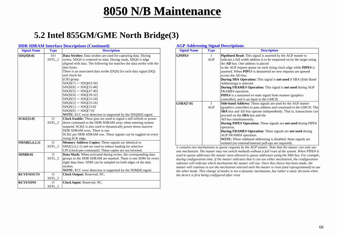
8050 8050 N/B MaintenanceN/B Maintenance
68
DDR SDRAM Interface Descriptions (Continued) Signal Name Type Description
SDQS[8:0] I/O SSTL_2
Data Strobes: Data strobes are used for capturing data. During writes, SDQS is centered on data. During reads, SDQS is edge aligned with data. The following list matches the data strobe with the data bytes. There is an associated data strobe (DQS) for each data signal (DQ) and check bit (CB) group. SDQS[7] -> SDQ[63:56] SDQS[6] -> SDQ[55:48] SDQS[5] -> SDQ[47:40] SDQS[4] -> SDQ[39:32] SDQS[3] -> SDQ[31:24] SDQS[2] -> SDQ[23:16] SDQS[1] -> SDQ[15:8] SDQS[0] -> SDQ[7:0] NOTE: ECC error detection is supported by the SDQS[8] signal.
SCKE[3:0] O SSTL_2
Clock Enable: These pins are used to signal a self-refresh or power down command to the DDR SDRAM array when entering system suspend. SCKE is also used to dynamically power down inactive DDR SDRAM rows. There is one SCKE per DDR SDRAM row. These signals can be toggled on every rising SCK edge.
SMAB[5,4,2,1] O SSTL_2
Memory Address Copies: These signals are identical to SMA[5,4,2,1] and are used to reduce loading for selective CPC(clock-per-command). These copies are not inverted.
SDM[8:0] O SSTL_2
Data Mask: When activated during writes, the corresponding data groups in the DDR SDRAM are masked. There is one SDM for every eight data lines. SDM can be sampled on both edges of the data strobes. NOTE: ECC error detection is supported by the SDM[8] signal.
RCVENOUT# O SSTL_2
Clock Output: Reserved, NC.
RCVENIN# O SSTL_2
Clock Input: Reserved, NC.
AGP Addressing Signal Descriptions Signal Name Type Description
GPIPE# I AGP
Pipelined Read: This signal is asserted by the AGP master to indicate a full width address is to be enqueued on by the target using the AD bus. One address is placed in the AGP request queue on each rising clock edge while PIPE# is asserted. When PIPE# is deasserted no new requests are queued across the AD bus. During SBA Operation: This signal is not used if SBA (Side Band Addressing) is selected. During FRAME# Operation: This signal is not used during AGP FRAME# operation. PIPE# is a sustained tri-state signal from masters (graphics controller), and is an input to the GMCH.
GSBA[7:0] I AGP
Side-band Address: These signals are used by the AGP master (graphics controller) to pass address and command to the GMCH. The SBA bus and AD bus operate independently. That is, transactions can proceed on the SBA bus and the AD bus simultaneously. During PIPE# Operation: These signals are not used during PIPE# operation. During FRAME# Operation: These signals are not used during AGP FRAME# operation. NOTE: When sideband addressing is disabled, these signals are isolated (no external/internal pull-ups are required).
5 contains two mechanisms to queue requests by the AGP master. Note that the master can only use one mechanism. The master may not switch methods without a full reset of the system. When PIPE# is used to queue addresses the master isnot allowed to queue addresses using the SBA bus. For example, during configuration time, if the master indicates that it can use either mechanism, the configuration software will indicate which mechanism the master will use. Once this choice has been made, the master will continue to use the mechanism selected until the master is reset (and reprogrammed) to use the other mode. This change of modes is not a dynamic mechanism, but rather a static decision when the device is first being configured after reset
5.2 Intel 855GM/GME North Bridge(3)
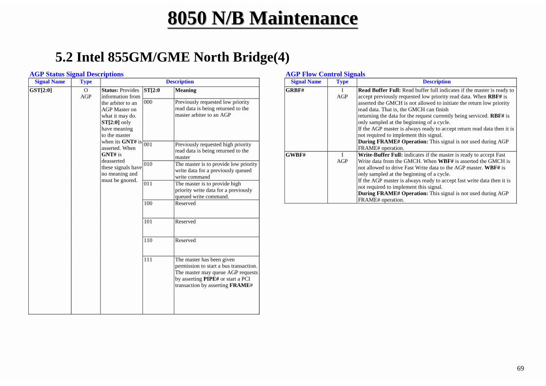
8050 8050 N/B MaintenanceN/B Maintenance
69
AGP Flow Control Signals Signal Name Type Description
GRBF# I AGP
Read Buffer Full: Read buffer full indicates if the master is ready to accept previously requested low priority read data. When RBF# is asserted the GMCH is not allowed to initiate the return low priority read data. That is, the GMCH can finish returning the data for the request currently being serviced. RBF# is only sampled at the beginning of a cycle. If the AGP master is always ready to accept return read data then it is not required to implement this signal. During FRAME# Operation: This signal is not used during AGP FRAME# operation.
GWBF# I AGP
Write-Buffer Full: indicates if the master is ready to accept Fast Write data from the GMCH. When WBF# is asserted the GMCH is not allowed to drive Fast Write data to the AGP master. WBF# is only sampled at the beginning of a cycle. If the AGP master is always ready to accept fast write data then it is not required to implement this signal. During FRAME# Operation: This signal is not used during AGP FRAME# operation.
AGP Status Signal Descriptions Signal Name Type Description
ST[2:0 Meaning
000 Previously requested low priority read data is being returned to the master arbiter to an AGP
001 Previously requested high priority read data is being returned to the master
010 The master is to provide low priority write data for a previously queued write command
011 The master is to provide high priority write data for a previously queued write command.
100 Reserved
101 Reserved
110 Reserved
GST[2:0] O AGP
Status: Provides information from the arbiter to an AGP Master on what it may do. ST[2:0] only have meaning to the master when its GNT# is asserted. When GNT# is deasserted these signals have no meaning and must be gnored.
111 The master has been given permission to start a bus transaction. The master may queue AGP requests by asserting PIPE# or start a PCI transaction by asserting FRAME#
5.2 Intel 855GM/GME North Bridge(4)
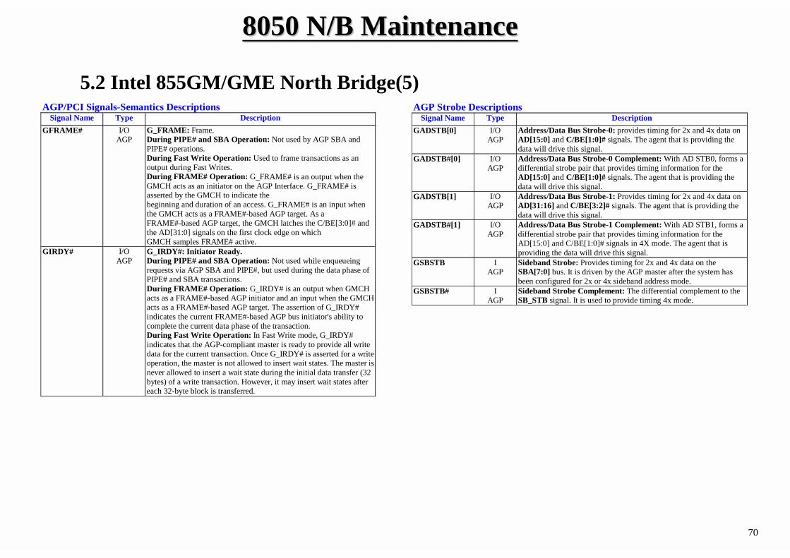
8050 8050 N/B MaintenanceN/B Maintenance
70
AGP Strobe Descriptions Signal Name Type Description
GADSTB[0] I/O AGP
Address/Data Bus Strobe-0: provides timing for 2x and 4x data on AD[15:0] and C/BE[1:0]# signals. The agent that is providing the data will drive this signal.
GADSTB#[0] I/O AGP
Address/Data Bus Strobe-0 Complement: With AD STB0, forms a differential strobe pair that provides timing information for the AD[15:0] and C/BE[1:0]# signals. The agent that is providing the data will drive this signal.
GADSTB[1] I/O AGP
Address/Data Bus Strobe-1: Provides timing for 2x and 4x data on AD[31:16] and C/BE[3:2]# signals. The agent that is providing the data will drive this signal.
GADSTB#[1] I/O AGP
Address/Data Bus Strobe-1 Complement: With AD STB1, forms a differential strobe pair that provides timing information for the AD[15:0] and C/BE[1:0]# signals in 4X mode. The agent that is providing the data will drive this signal.
GSBSTB I AGP
Sideband Strobe: Provides timing for 2x and 4x data on the SBA[7:0] bus. It is driven by the AGP master after the system has been configured for 2x or 4x sideband address mode.
GSBSTB# I AGP
Sideband Strobe Complement: The differential complement to the SB_STB signal. It is used to provide timing 4x mode.
AGP/PCI Signals-Semantics Descriptions Signal Name Type Description
GFRAME# I/O AGP
G_FRAME: Frame. During PIPE# and SBA Operation: Not used by AGP SBA and PIPE# operations. During Fast Write Operation: Used to frame transactions as an output during Fast Writes. During FRAME# Operation: G_FRAME# is an output when the GMCH acts as an initiator on the AGP Interface. G_FRAME# is asserted by the GMCH to indicate the beginning and duration of an access. G_FRAME# is an input when the GMCH acts as a FRAME#-based AGP target. As a FRAME#-based AGP target, the GMCH latches the C/BE[3:0]# and the AD[31:0] signals on the first clock edge on which GMCH samples FRAME# active.
GIRDY# I/O AGP
G_IRDY#: Initiator Ready. During PIPE# and SBA Operation: Not used while enqueueing requests via AGP SBA and PIPE#, but used during the data phase of PIPE# and SBA transactions. During FRAME# Operation: G_IRDY# is an output when GMCH acts as a FRAME#-based AGP initiator and an input when the GMCH acts as a FRAME#-based AGP target. The assertion of G_IRDY# indicates the current FRAME#-based AGP bus initiator's ability to complete the current data phase of the transaction. During Fast Write Operation: In Fast Write mode, G_IRDY# indicates that the AGP-compliant master is ready to provide all write data for the current transaction. Once G_IRDY# is asserted for a write operation, the master is not allowed to insert wait states. The master is never allowed to insert a wait state during the initial data transfer (32 bytes) of a write transaction. However, it may insert wait states aftereach 32-byte block is transferred.
5.2 Intel 855GM/GME North Bridge(5)
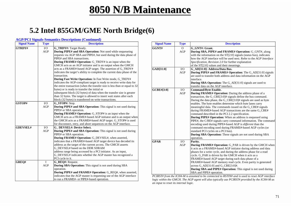
8050 8050 N/B MaintenanceN/B Maintenance
71
AGP/PCI Signals-Semantics Descriptions (Continued) Signal Name Type Description
GTRDY# I/O AGP
G_TRDY#: Target Ready. During PIPE# and SBA Operation: Not used while enqueueing requests via AGP SBA and PIPE#, but used during the data phase of PIPE# and SBA transactions. During FRAME# Operation: G_TRDY# is an input when the GMCH acts as an AGP initiator and is an output when the GMCH acts as a FRAME#-based AGP target. The assertion of G_TRDY# indicates the target’s ability to complete the current data phase of the transaction. During Fast Write Operation: In Fast Write mode, G_TRDY# indicates the AGP-compliant target is ready to receive write data for the entire transaction (when the transfer size is less than or equal to 32 bytes) or is ready to transfer the initial or subsequent block (32 bytes) of data when the transfer size is greater than 32 bytes. The target is allowed to insert wait states after each block (32 bytes) is transferred on write transactions.
GSTOP# I/O AGP
G_STOP#: Stop. During PIPE# and SBA Operation: This signal is not used during PIPE# or SBA operation. During FRAME# Operation: G_STOP# is an input when the GMCH acts as a FRAME#-based AGP initiator and is an output when the GMCH acts as a FRAME#-based AGP target. G_STOP# is used for disconnect, retry, and abort sequences on the AGP interface.
GDEVSEL# I/O AGP
G_ DEVSEL#: Device Select. During PIPE# and SBA Operation: This signal is not used during PIPE# or SBA operation. During FRAME# Operation: G_DEVSEL#, when asserted, indicates that a FRAME#-based AGP target device has decoded its address as the target of the current access. The GMCH asserts G_DEVSEL# based on the DDR SDRAM address range being accessed by a PCI initiator. As an input, G_DEVSEL# indicates whether the AGP master has recognized a PCI cycle to it.
GREQ# I AGP
G_REQ#: Request. During SBA Operation: This signal is not used during SBA operation. During PIPE# and FRAME# Operation: G_REQ#, when asserted, indicates that the AGP master is requesting use of the AGP interface to run a FRAME#- or PIPE#-based operation.
Signal Name Type Description GGNT# O
AGP G_GNT#: Grant. During SBA, PIPE# and FRAME# Operation: G_GNT#, along with the information on the ST[2:0] signals (status bus), indicates how the AGP interface will be used next. Refer to the AGP Interface Specification, Revision 2.0 for further explanation of the ST[2:0] values and their meanings.
GAD[31:0] I/O AGP
G_AD[31:0]: Address/Data Bus. During PIPE# and FRAME# Operation: The G_AD[31:0] signals are used to transfer both address and data information on the AGP interface. During SBA Operation: The G_AD[31:0] signals are used to transfer data on the AGP interface.
GCBE#[3:0] I/O AGP
Command/Byte Enable. During FRAME# Operation: During the address phase of a transaction, the G_CBE[3:0]# signals define the bus command. During the data phase, the G_CBE[3:0]# signals are used as byte enables. The byte enables determine which byte lanes carry meaningful data. The commands issued on the G_CBE# signals during FRAME#-based AGP transactions are the same G_CBE# command described in the PCI 2.2 specification. During PIPE# Operation: When an address is enqueued using PIPE#, the C/BE# signals carry command information. The command encoding used during PIPE#-based AGP is different than the command encoding used during FRAME#-based AGP cycles (or standard PCI cycles on a PCI bus). During SBA Operation: These signals are not used during SBA operation.
GPAR I/O AGP
Parity. During FRAME# Operation: G_PAR is driven by the GMCH when it acts as a FRAME#-based AGP initiator during address and data phases for a write cycle, and during the address phase for a read cycle. G_PAR is driven by the GMCH when it acts as a FRAME#-based AGP target during each data phase of a FRAME#-based AGP memory read cycle. Even parity is generated across G_AD[31:0] and G_CBE[3:0]#. During SBA and PIPE# Operation: This signal is not used during SBA and PIPE# operation.
PCIRST# from the ICH4-M is assumed to be connected to RSTIN# and is used to reset AGP interface logic within the GMCH. The AGP agent will also typically use PCIRST# provided by the ICH4-M as an input to reset its internal logic.
5.2 Intel 855GM/GME North Bridge(6)
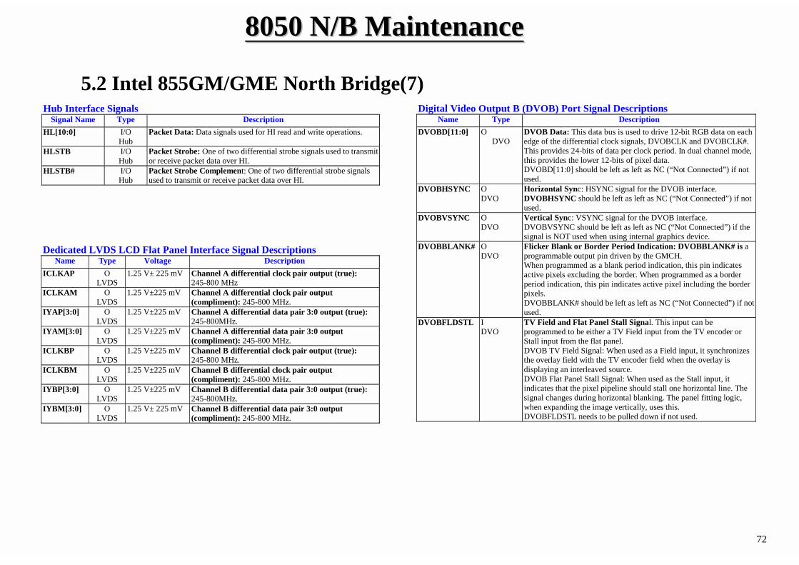
8050 8050 N/B MaintenanceN/B Maintenance
72
Hub Interface Signals Signal Name Type Description
HL[10:0] I/O Hub
Packet Data: Data signals used for HI read and write operations.
HLSTB I/O Hub
Packet Strobe: One of two differential strobe signals used to transmit or receive packet data over HI.
HLSTB# I/O Hub
Packet Strobe Complement: One of two differential strobe signals used to transmit or receive packet data over HI.
Dedicated LVDS LCD Flat Panel Interface Signal Descriptions Name Type Voltage Description
ICLKAP O LVDS
1.25 V± 225 mV Channel A differential clock pair output (true): 245-800 MHz
ICLKAM O LVDS
1.25 V±225 mV Channel A differential clock pair output (compliment): 245-800 MHz.
IYAP[3:0] O LVDS
1.25 V±225 mV Channel A differential data pair 3:0 output (true): 245-800MHz.
IYAM[3:0] O LVDS
1.25 V±225 mV Channel A differential data pair 3:0 output (compliment): 245-800 MHz.
ICLKBP O LVDS
1.25 V±225 mV Channel B differential clock pair output (true): 245-800 MHz.
ICLKBM O LVDS
1.25 V±225 mV Channel B differential clock pair output (compliment): 245-800 MHz.
IYBP[3:0] O LVDS
1.25 V±225 mV Channel B differential data pair 3:0 output (true): 245-800MHz.
IYBM[3:0] O LVDS
1.25 V± 225 mV Channel B differential data pair 3:0 output (compliment): 245-800 MHz.
Digital Video Output B (DVOB) Port Signal Descriptions Name Type Description
DVOBD[11:0] O DVO
DVOB Data: This data bus is used to drive 12-bit RGB data on each edge of the differential clock signals, DVOBCLK and DVOBCLK#. This provides 24-bits of data per clock period. In dual channel mode, this provides the lower 12-bits of pixel data. DVOBD[11:0] should be left as left as NC (“Not Connected”) if not used.
DVOBHSYNC O DVO
Horizontal Sync: HSYNC signal for the DVOB interface. DVOBHSYNC should be left as left as NC (“Not Connected”) if not used.
DVOBVSYNC O DVO
Vertical Sync: VSYNC signal for the DVOB interface. DVOBVSYNC should be left as left as NC (“Not Connected”) if the signal is NOT used when using internal graphics device.
DVOBBLANK# O DVO
Flicker Blank or Border Period Indication: DVOBBLANK# is a programmable output pin driven by the GMCH. When programmed as a blank period indication, this pin indicates active pixels excluding the border. When programmed as a border period indication, this pin indicates active pixel including the border pixels. DVOBBLANK# should be left as left as NC (“Not Connected”) if not used.
DVOBFLDSTL I DVO
TV Field and Flat Panel Stall Signal. This input can be programmed to be either a TV Field input from the TV encoder or Stall input from the flat panel. DVOB TV Field Signal: When used as a Field input, it synchronizes the overlay field with the TV encoder field when the overlay is displaying an interleaved source. DVOB Flat Panel Stall Signal: When used as the Stall input, it indicates that the pixel pipeline should stall one horizontal line. The signal changes during horizontal blanking. The panel fitting logic, when expanding the image vertically, uses this. DVOBFLDSTL needs to be pulled down if not used.
5.2 Intel 855GM/GME North Bridge(7)
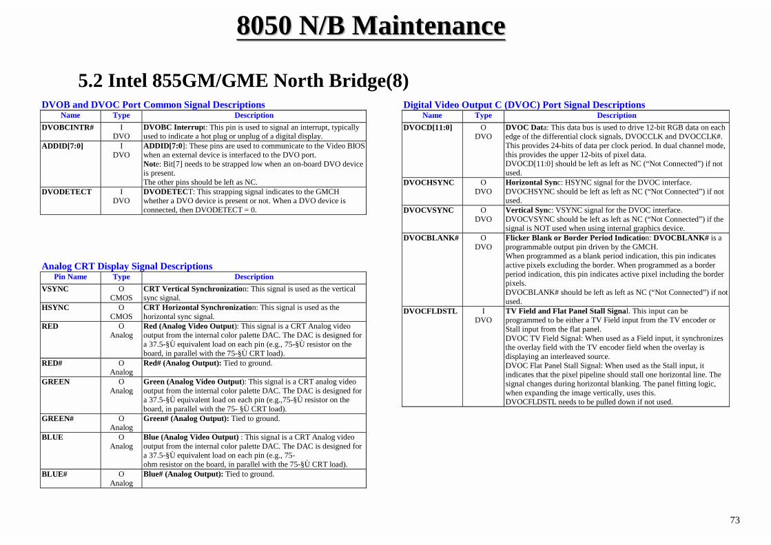
8050 8050 N/B MaintenanceN/B Maintenance
73
Digital Video Output C (DVOC) Port Signal Descriptions Name Type Description
DVOCD[11:0] O DVO
DVOC Data: This data bus is used to drive 12-bit RGB data on each edge of the differential clock signals, DVOCCLK and DVOCCLK#. This provides 24-bits of data per clock period. In dual channel mode, this provides the upper 12-bits of pixel data. DVOCD[11:0] should be left as left as NC (“Not Connected”) if not used.
DVOCHSYNC O DVO
Horizontal Sync: HSYNC signal for the DVOC interface. DVOCHSYNC should be left as left as NC (“Not Connected”) if not used.
DVOCVSYNC O DVO
Vertical Sync: VSYNC signal for the DVOC interface. DVOCVSYNC should be left as left as NC (“Not Connected”) if the signal is NOT used when using internal graphics device.
DVOCBLANK# O DVO
Flicker Blank or Border Period Indication: DVOCBLANK# is a programmable output pin driven by the GMCH. When programmed as a blank period indication, this pin indicates active pixels excluding the border. When programmed as a border period indication, this pin indicates active pixel including the border pixels. DVOCBLANK# should be left as left as NC (“Not Connected”) if not used.
DVOCFLDSTL I DVO
TV Field and Flat Panel Stall Signal. This input can be programmed to be either a TV Field input from the TV encoder or Stall input from the flat panel. DVOC TV Field Signal: When used as a Field input, it synchronizes the overlay field with the TV encoder field when the overlay is displaying an interleaved source. DVOC Flat Panel Stall Signal: When used as the Stall input, it indicates that the pixel pipeline should stall one horizontal line. The signal changes during horizontal blanking. The panel fitting logic, when expanding the image vertically, uses this. DVOCFLDSTL needs to be pulled down if not used.
DVOB and DVOC Port Common Signal Descriptions Name Type Description
DVOBCINTR# I DVO
DVOBC Interrupt: This pin is used to signal an interrupt, typically used to indicate a hot plug or unplug of a digital display.
ADDID[7:0] I DVO
ADDID[7:0]: These pins are used to communicate to the Video BIOS when an external device is interfaced to the DVO port. Note: Bit[7] needs to be strapped low when an on-board DVO device is present. The other pins should be left as NC.
DVODETECT I DVO
DVODETECT: This strapping signal indicates to the GMCH whether a DVO device is present or not. When a DVO device is connected, then DVODETECT = 0.
Analog CRT Display Signal Descriptions Pin Name Type Description
VSYNC O CMOS
CRT Vertical Synchronization: This signal is used as the vertical sync signal.
HSYNC O CMOS
CRT Horizontal Synchronization: This signal is used as the horizontal sync signal.
RED O Analog
Red (Analog Video Output): This signal is a CRT Analog video output from the internal color palette DAC. The DAC is designed for a 37.5-§Ù equivalent load on each pin (e.g., 75-§Ù resistor on the board, in parallel with the 75-§Ù CRT load).
RED# O Analog
Red# (Analog Output): Tied to ground.
GREEN O Analog
Green (Analog Video Output): This signal is a CRT analog video output from the internal color palette DAC. The DAC is designed for a 37.5-§Ù equivalent load on each pin (e.g.,75-§Ù resistor on the board, in parallel with the 75- §Ù CRT load).
GREEN# O Analog
Green# (Analog Output): Tied to ground.
BLUE O Analog
Blue (Analog Video Output) : This signal is a CRT Analog video output from the internal color palette DAC. The DAC is designed for a 37.5-§Ù equivalent load on each pin (e.g., 75- ohm resistor on the board, in parallel with the 75-§Ù CRT load).
BLUE# O Analog
Blue# (Analog Output): Tied to ground.
5.2 Intel 855GM/GME North Bridge(8)
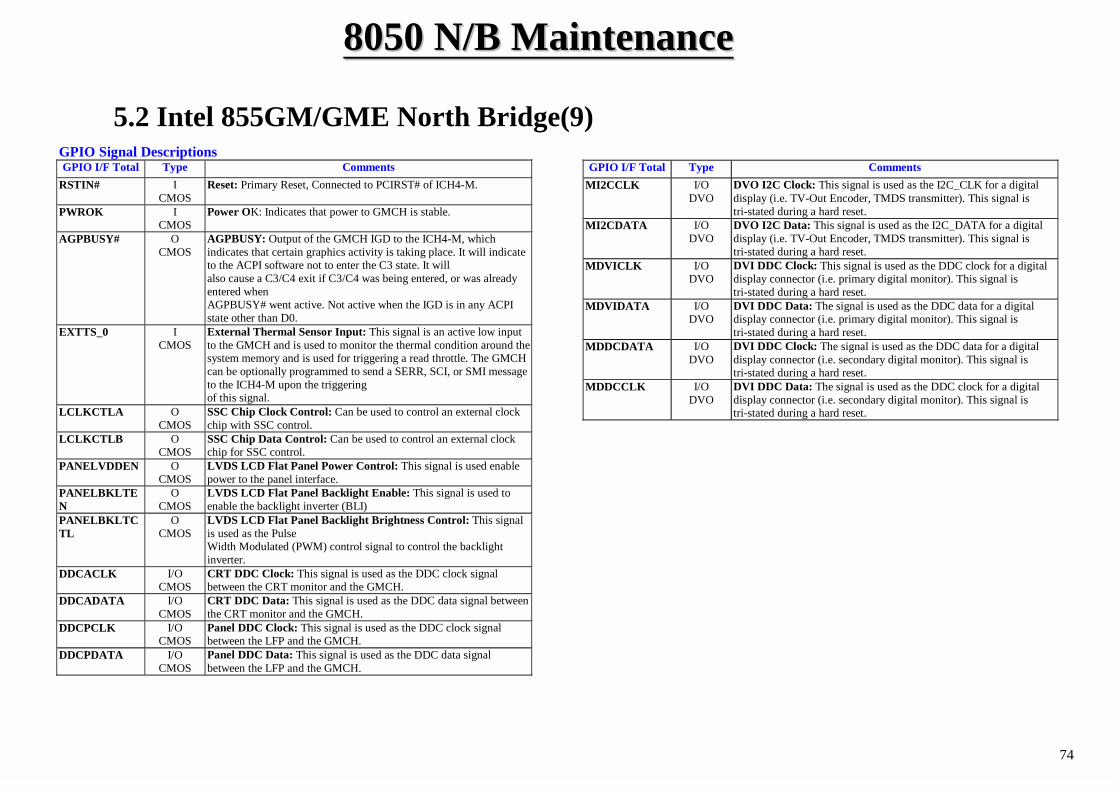
8050 8050 N/B MaintenanceN/B Maintenance
74
GPIO Signal Descriptions
GPIO I/F Total Type Comments RSTIN# I
CMOS Reset: Primary Reset, Connected to PCIRST# of ICH4-M.
PWROK I CMOS
Power OK: Indicates that power to GMCH is stable.
AGPBUSY# O CMOS
AGPBUSY: Output of the GMCH IGD to the ICH4-M, which indicates that certain graphics activity is taking place. It will indicate to the ACPI software not to enter the C3 state. It will also cause a C3/C4 exit if C3/C4 was being entered, or was already entered when AGPBUSY# went active. Not active when the IGD is in any ACPI state other than D0.
EXTTS_0 I CMOS
External Thermal Sensor Input: This signal is an active low input to the GMCH and is used to monitor the thermal condition around the system memory and is used for triggering a read throttle. The GMCH can be optionally programmed to send a SERR, SCI, or SMI message to the ICH4-M upon the triggering of this signal.
LCLKCTLA O CMOS
SSC Chip Clock Control: Can be used to control an external clock chip with SSC control.
LCLKCTLB O CMOS
SSC Chip Data Control: Can be used to control an external clock chip for SSC control.
PANELVDDEN O CMOS
LVDS LCD Flat Panel Power Control: This signal is used enable power to the panel interface.
PANELBKLTEN
O CMOS
LVDS LCD Flat Panel Backlight Enable: This signal is used to enable the backlight inverter (BLI)
PANELBKLTCTL
O CMOS
LVDS LCD Flat Panel Backlight Brightness Control: This signal is used as the Pulse Width Modulated (PWM) control signal to control the backlight inverter.
DDCACLK I/O CMOS
CRT DDC Clock: This signal is used as the DDC clock signal between the CRT monitor and the GMCH.
DDCADATA I/O CMOS
CRT DDC Data: This signal is used as the DDC data signal between the CRT monitor and the GMCH.
DDCPCLK I/O CMOS
Panel DDC Clock: This signal is used as the DDC clock signal between the LFP and the GMCH.
DDCPDATA I/O CMOS
Panel DDC Data: This signal is used as the DDC data signal between the LFP and the GMCH.
GPIO I/F Total Type Comments MI2CCLK I/O
DVO DVO I2C Clock: This signal is used as the I2C_CLK for a digital display (i.e. TV-Out Encoder, TMDS transmitter). This signal is tri-stated during a hard reset.
MI2CDATA I/O DVO
DVO I2C Data: This signal is used as the I2C_DATA for a digital display (i.e. TV-Out Encoder, TMDS transmitter). This signal is tri-stated during a hard reset.
MDVICLK I/O DVO
DVI DDC Clock: This signal is used as the DDC clock for a digital display connector (i.e. primary digital monitor). This signal is tri-stated during a hard reset.
MDVIDATA I/O DVO
DVI DDC Data: The signal is used as the DDC data for a digital display connector (i.e. primary digital monitor). This signal is tri-stated during a hard reset.
MDDCDATA I/O DVO
DVI DDC Clock: The signal is used as the DDC data for a digital display connector (i.e. secondary digital monitor). This signal is tri-stated during a hard reset.
MDDCCLK I/O DVO
DVI DDC Data: The signal is used as the DDC clock for a digital display connector (i.e. secondary digital monitor). This signal is tri-stated during a hard reset.
5.2 Intel 855GM/GME North Bridge(9)
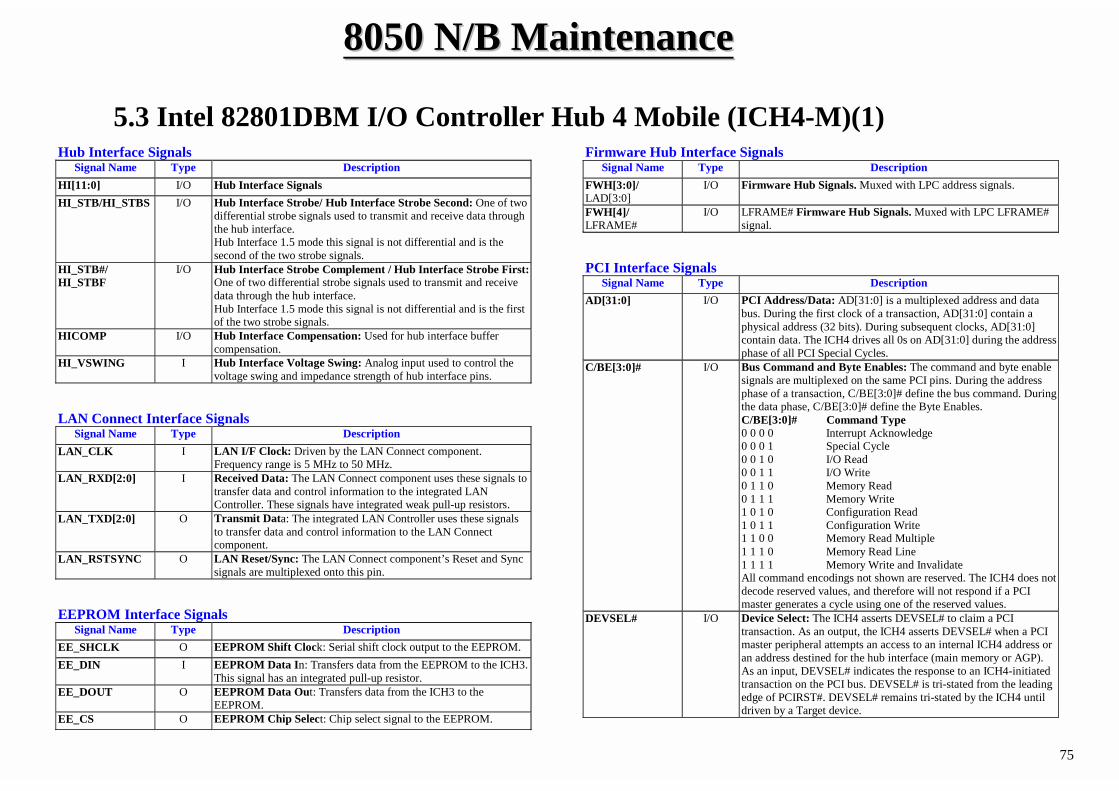
8050 8050 N/B MaintenanceN/B Maintenance
75
Hub Interface Signals Signal Name Type Description
HI[11:0] I/O Hub Interface Signals HI_STB/HI_STBS I/O Hub Interface Strobe/ Hub Interface Strobe Second: One of two
differential strobe signals used to transmit and receive data through the hub interface. Hub Interface 1.5 mode this signal is not differential and is the second of the two strobe signals.
HI_STB#/ HI_STBF
I/O Hub Interface Strobe Complement / Hub Interface Strobe First: One of two differential strobe signals used to transmit and receive data through the hub interface. Hub Interface 1.5 mode this signal is not differential and is the first of the two strobe signals.
HICOMP I/O Hub Interface Compensation: Used for hub interface buffer compensation.
HI_VSWING I Hub Interface Voltage Swing: Analog input used to control the voltage swing and impedance strength of hub interface pins.
LAN Connect Interface Signals
Signal Name Type Description LAN_CLK I LAN I/F Clock: Driven by the LAN Connect component.
Frequency range is 5 MHz to 50 MHz. LAN_RXD[2:0] I Received Data: The LAN Connect component uses these signals to
transfer data and control information to the integrated LAN Controller. These signals have integrated weak pull-up resistors.
LAN_TXD[2:0] O Transmit Data: The integrated LAN Controller uses these signals to transfer data and control information to the LAN Connect component.
LAN_RSTSYNC O LAN Reset/Sync: The LAN Connect component’s Reset and Sync signals are multiplexed onto this pin.
EEPROM Interface Signals
Signal Name Type Description EE_SHCLK O EEPROM Shift Clock: Serial shift clock output to the EEPROM.EE_DIN I EEPROM Data In: Transfers data from the EEPROM to the ICH3.
This signal has an integrated pull-up resistor. EE_DOUT O EEPROM Data Out: Transfers data from the ICH3 to the
EEPROM. EE_CS O EEPROM Chip Select: Chip select signal to the EEPROM.
Firmware Hub Interface Signals Signal Name Type Description
FWH[3:0]/ LAD[3:0]
I/O Firmware Hub Signals. Muxed with LPC address signals.
FWH[4]/ LFRAME#
I/O LFRAME# Firmware Hub Signals. Muxed with LPC LFRAME# signal.
PCI Interface Signals
Signal Name Type Description AD[31:0] I/O PCI Address/Data: AD[31:0] is a multiplexed address and data
bus. During the first clock of a transaction, AD[31:0] contain a physical address (32 bits). During subsequent clocks, AD[31:0] contain data. The ICH4 drives all 0s on AD[31:0] during the address phase of all PCI Special Cycles.
C/BE[3:0]# I/O Bus Command and Byte Enables: The command and byte enable signals are multiplexed on the same PCI pins. During the address phase of a transaction, C/BE[3:0]# define the bus command. During the data phase, C/BE[3:0]# define the Byte Enables. C/BE[3:0]# Command Type 0 0 0 0 Interrupt Acknowledge 0 0 0 1 Special Cycle 0 0 1 0 I/O Read 0 0 1 1 I/O Write 0 1 1 0 Memory Read 0 1 1 1 Memory Write 1 0 1 0 Configuration Read 1 0 1 1 Configuration Write 1 1 0 0 Memory Read Multiple 1 1 1 0 Memory Read Line 1 1 1 1 Memory Write and Invalidate All command encodings not shown are reserved. The ICH4 does not decode reserved values, and therefore will not respond if a PCI master generates a cycle using one of the reserved values.
DEVSEL# I/O Device Select: The ICH4 asserts DEVSEL# to claim a PCI transaction. As an output, the ICH4 asserts DEVSEL# when a PCI master peripheral attempts an access to an internal ICH4 address or an address destined for the hub interface (main memory or AGP). As an input, DEVSEL# indicates the response to an ICH4-initiated transaction on the PCI bus. DEVSEL# is tri-stated from the leading edge of PCIRST#. DEVSEL# remains tri-stated by the ICH4 until driven by a Target device.
5.3 Intel 82801DBM I/O Controller Hub 4 Mobile (ICH4-M)(1)
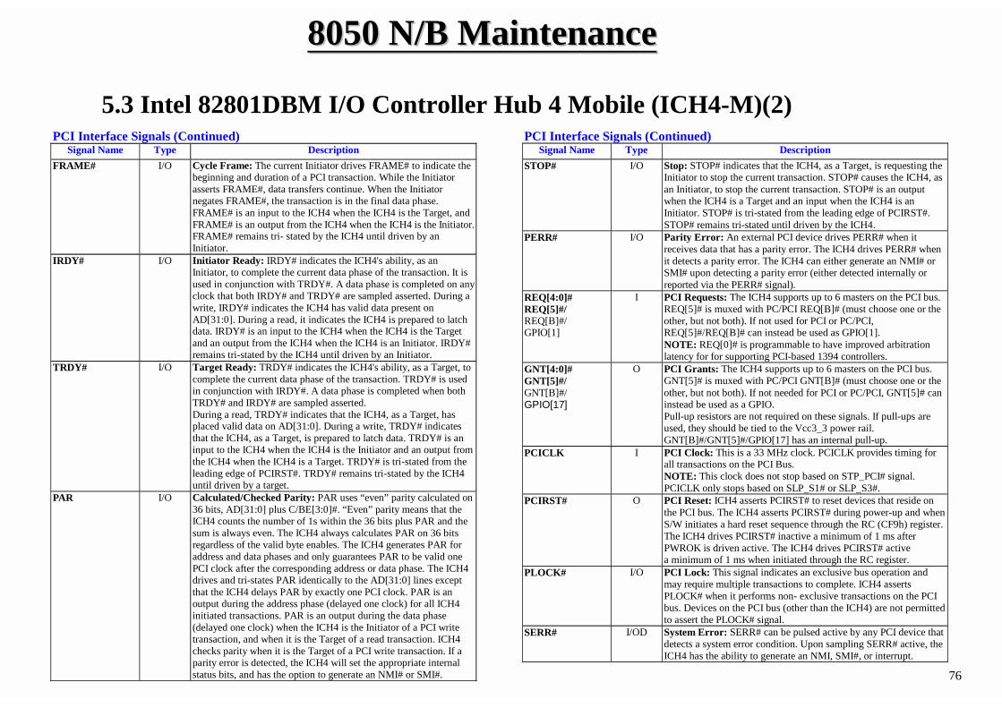
8050 8050 N/B MaintenanceN/B Maintenance
76
PCI Interface Signals (Continued) Signal Name Type Description
FRAME# I/O Cycle Frame: The current Initiator drives FRAME# to indicate the beginning and duration of a PCI transaction. While the Initiator asserts FRAME#, data transfers continue. When the Initiator negates FRAME#, the transaction is in the final data phase. FRAME# is an input to the ICH4 when the ICH4 is the Target, andFRAME# is an output from the ICH4 when the ICH4 is the Initiator. FRAME# remains tri- stated by the ICH4 until driven by an Initiator.
IRDY# I/O Initiator Ready: IRDY# indicates the ICH4's ability, as an Initiator, to complete the current data phase of the transaction. It is used in conjunction with TRDY#. A data phase is completed on any clock that both IRDY# and TRDY# are sampled asserted. During a write, IRDY# indicates the ICH4 has valid data present on AD[31:0]. During a read, it indicates the ICH4 is prepared to latch data. IRDY# is an input to the ICH4 when the ICH4 is the Target and an output from the ICH4 when the ICH4 is an Initiator. IRDY# remains tri-stated by the ICH4 until driven by an Initiator.
TRDY# I/O Target Ready: TRDY# indicates the ICH4's ability, as a Target, to complete the current data phase of the transaction. TRDY# is used in conjunction with IRDY#. A data phase is completed when both TRDY# and IRDY# are sampled asserted. During a read, TRDY# indicates that the ICH4, as a Target, has placed valid data on AD[31:0]. During a write, TRDY# indicates that the ICH4, as a Target, is prepared to latch data. TRDY# is an input to the ICH4 when the ICH4 is the Initiator and an output from the ICH4 when the ICH4 is a Target. TRDY# is tri-stated from the leading edge of PCIRST#. TRDY# remains tri-stated by the ICH4 until driven by a target.
PAR I/O Calculated/Checked Parity: PAR uses “even” parity calculated on 36 bits, AD[31:0] plus C/BE[3:0]#. “Even” parity means that the ICH4 counts the number of 1s within the 36 bits plus PAR and the sum is always even. The ICH4 always calculates PAR on 36 bits regardless of the valid byte enables. The ICH4 generates PAR for address and data phases and only guarantees PAR to be valid one PCI clock after the corresponding address or data phase. The ICH4 drives and tri-states PAR identically to the AD[31:0] lines except that the ICH4 delays PAR by exactly one PCI clock. PAR is an output during the address phase (delayed one clock) for all ICH4 initiated transactions. PAR is an output during the data phase (delayed one clock) when the ICH4 is the Initiator of a PCI write transaction, and when it is the Target of a read transaction. ICH4 checks parity when it is the Target of a PCI write transaction. If a parity error is detected, the ICH4 will set the appropriate internal status bits, and has the option to generate an NMI# or SMI#.
PCI Interface Signals (Continued)Signal Name Type Description
STOP# I/O Stop: STOP# indicates that the ICH4, as a Target, is requesting the Initiator to stop the current transaction. STOP# causes the ICH4, as an Initiator, to stop the current transaction. STOP# is an output when the ICH4 is a Target and an input when the ICH4 is an Initiator. STOP# is tri-stated from the leading edge of PCIRST#. STOP# remains tri-stated until driven by the ICH4.
PERR# I/O Parity Error: An external PCI device drives PERR# when it receives data that has a parity error. The ICH4 drives PERR# when it detects a parity error. The ICH4 can either generate an NMI# or SMI# upon detecting a parity error (either detected internally or reported via the PERR# signal).
REQ[4:0]# REQ[5]#/ REQ[B]#/ GPIO[1]
I PCI Requests: The ICH4 supports up to 6 masters on the PCI bus. REQ[5]# is muxed with PC/PCI REQ[B]# (must choose one or the other, but not both). If not used for PCI or PC/PCI, REQ[5]#/REQ[B]# can instead be used as GPIO[1]. NOTE: REQ[0]# is programmable to have improved arbitration latency for for supporting PCI-based 1394 controllers.
GNT[4:0]# GNT[5]#/ GNT[B]#/ GPIO[17]
O PCI Grants: The ICH4 supports up to 6 masters on the PCI bus. GNT[5]# is muxed with PC/PCI GNT[B]# (must choose one or the other, but not both). If not needed for PCI or PC/PCI, GNT[5]# can instead be used as a GPIO. Pull-up resistors are not required on these signals. If pull-ups are used, they should be tied to the Vcc3_3 power rail. GNT[B]#/GNT[5]#/GPIO[17] has an internal pull-up.
PCICLK I PCI Clock: This is a 33 MHz clock. PCICLK provides timing for all transactions on the PCI Bus. NOTE: This clock does not stop based on STP_PCI# signal. PCICLK only stops based on SLP_S1# or SLP_S3#.
PCIRST# O PCI Reset: ICH4 asserts PCIRST# to reset devices that reside on the PCI bus. The ICH4 asserts PCIRST# during power-up and when S/W initiates a hard reset sequence through the RC (CF9h) register. The ICH4 drives PCIRST# inactive a minimum of 1 ms after PWROK is driven active. The ICH4 drives PCIRST# active a minimum of 1 ms when initiated through the RC register.
PLOCK# I/O PCI Lock: This signal indicates an exclusive bus operation and may require multiple transactions to complete. ICH4 asserts PLOCK# when it performs non- exclusive transactions on the PCI bus. Devices on the PCI bus (other than the ICH4) are not permitted to assert the PLOCK# signal.
SERR# I/OD System Error: SERR# can be pulsed active by any PCI device that detects a system error condition. Upon sampling SERR# active, the ICH4 has the ability to generate an NMI, SMI#, or interrupt.
5.3 Intel 82801DBM I/O Controller Hub 4 Mobile (ICH4-M)(2)
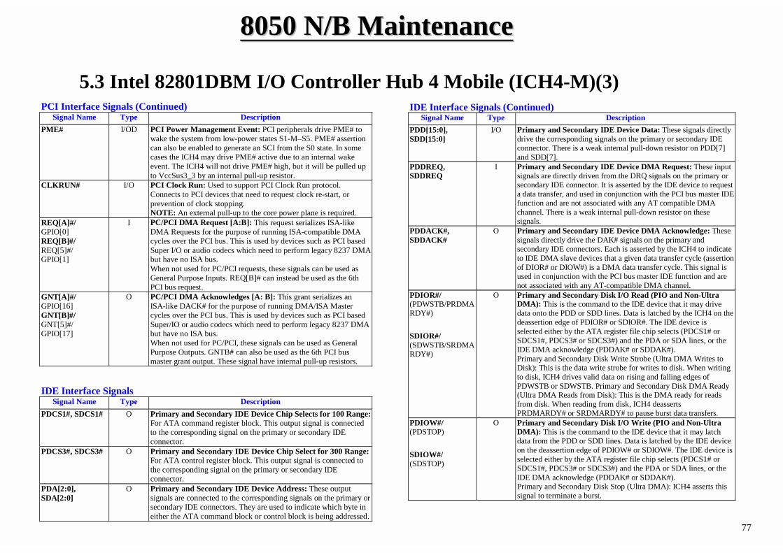
8050 8050 N/B MaintenanceN/B Maintenance
77
PCI Interface Signals (Continued) Signal Name Type Description
PME# I/OD PCI Power Management Event: PCI peripherals drive PME# to wake the system from low-power states S1-M–S5. PME# assertion can also be enabled to generate an SCI from the S0 state. In some cases the ICH4 may drive PME# active due to an internal wake event. The ICH4 will not drive PME# high, but it will be pulled upto VccSus3_3 by an internal pull-up resistor.
CLKRUN# I/O PCI Clock Run: Used to support PCI Clock Run protocol. Connects to PCI devices that need to request clock re-start, or prevention of clock stopping. NOTE: An external pull-up to the core power plane is required.
REQ[A]#/ GPIO[0] REQ[B]#/ REQ[5]#/ GPIO[1]
I PC/PCI DMA Request [A:B]: This request serializes ISA-like DMA Requests for the purpose of running ISA-compatible DMA cycles over the PCI bus. This is used by devices such as PCI based Super I/O or audio codecs which need to perform legacy 8237 DMA but have no ISA bus. When not used for PC/PCI requests, these signals can be used as General Purpose Inputs. REQ[B]# can instead be used as the 6th PCI bus request.
GNT[A]#/ GPIO[16] GNT[B]#/ GNT[5]#/ GPIO[17]
O PC/PCI DMA Acknowledges [A: B]: This grant serializes an ISA-like DACK# for the purpose of running DMA/ISA Master cycles over the PCI bus. This is used by devices such as PCI based Super/IO or audio codecs which need to perform legacy 8237 DMA but have no ISA bus. When not used for PC/PCI, these signals can be used as General Purpose Outputs. GNTB# can also be used as the 6th PCI bus master grant output. These signal have internal pull-up resistors.
IDE Interface Signals
Signal Name Type Description PDCS1#, SDCS1# O Primary and Secondary IDE Device Chip Selects for 100 Range:
For ATA command register block. This output signal is connected to the corresponding signal on the primary or secondary IDE connector.
PDCS3#, SDCS3# O Primary and Secondary IDE Device Chip Select for 300 Range: For ATA control register block. This output signal is connected to the corresponding signal on the primary or secondary IDE connector.
PDA[2:0], SDA[2:0]
O Primary and Secondary IDE Device Address: These output signals are connected to the corresponding signals on the primary or secondary IDE connectors. They are used to indicate which byte in either the ATA command block or control block is being addressed.
IDE Interface Signals (Continued)
Signal Name Type Description PDD[15:0], SDD[15:0]
I/O Primary and Secondary IDE Device Data: These signals directly drive the corresponding signals on the primary or secondary IDE connector. There is a weak internal pull-down resistor on PDD[7] and SDD[7].
PDDREQ, SDDREQ
I Primary and Secondary IDE Device DMA Request: These input signals are directly driven from the DRQ signals on the primary or secondary IDE connector. It is asserted by the IDE device to request a data transfer, and used in conjunction with the PCI bus master IDE function and are not associated with any AT compatible DMA channel. There is a weak internal pull-down resistor on these signals.
PDDACK#, SDDACK#
O Primary and Secondary IDE Device DMA Acknowledge: These signals directly drive the DAK# signals on the primary and secondary IDE connectors. Each is asserted by the ICH4 to indicate to IDE DMA slave devices that a given data transfer cycle (assertion of DIOR# or DIOW#) is a DMA data transfer cycle. This signal is used in conjunction with the PCI bus master IDE function and are not associated with any AT-compatible DMA channel.
PDIOR#/ (PDWSTB/PRDMARDY#) SDIOR#/ (SDWSTB/SRDMARDY#)
O Primary and Secondary Disk I/O Read (PIO and Non-Ultra DMA): This is the command to the IDE device that it may drive data onto the PDD or SDD lines. Data is latched by the ICH4 on the deassertion edge of PDIOR# or SDIOR#. The IDE device is selected either by the ATA register file chip selects (PDCS1# or SDCS1#, PDCS3# or SDCS3#) and the PDA or SDA lines, or the IDE DMA acknowledge (PDDAK# or SDDAK#). Primary and Secondary Disk Write Strobe (Ultra DMA Writes to Disk): This is the data write strobe for writes to disk. When writing to disk, ICH4 drives valid data on rising and falling edges of PDWSTB or SDWSTB. Primary and Secondary Disk DMA Ready (Ultra DMA Reads from Disk): This is the DMA ready for reads from disk. When reading from disk, ICH4 deasserts PRDMARDY# or SRDMARDY# to pause burst data transfers.
PDIOW#/ (PDSTOP) SDIOW#/ (SDSTOP)
O Primary and Secondary Disk I/O Write (PIO and Non-Ultra DMA): This is the command to the IDE device that it may latch data from the PDD or SDD lines. Data is latched by the IDE device on the deassertion edge of PDIOW# or SDIOW#. The IDE device is selected either by the ATA register file chip selects (PDCS1# or SDCS1#, PDCS3# or SDCS3#) and the PDA or SDA lines, or the IDE DMA acknowledge (PDDAK# or SDDAK#). Primary and Secondary Disk Stop (Ultra DMA): ICH4 asserts this signal to terminate a burst.
5.3 Intel 82801DBM I/O Controller Hub 4 Mobile (ICH4-M)(3)
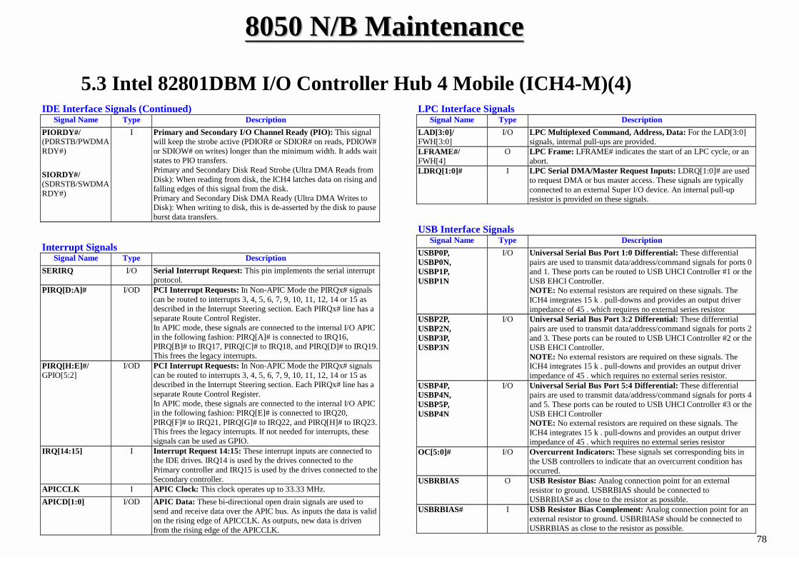
8050 8050 N/B MaintenanceN/B Maintenance
78
IDE Interface Signals (Continued) Signal Name Type Description
PIORDY#/ (PDRSTB/PWDMARDY#) SIORDY#/ (SDRSTB/SWDMARDY#)
I Primary and Secondary I/O Channel Ready (PIO): This signal will keep the strobe active (PDIOR# or SDIOR# on reads, PDIOW# or SDIOW# on writes) longer than the minimum width. It adds wait states to PIO transfers. Primary and Secondary Disk Read Strobe (Ultra DMA Reads from Disk): When reading from disk, the ICH4 latches data on rising and falling edges of this signal from the disk. Primary and Secondary Disk DMA Ready (Ultra DMA Writes to Disk): When writing to disk, this is de-asserted by the disk to pause burst data transfers.
Interrupt Signals
Signal Name Type Description SERIRQ I/O Serial Interrupt Request: This pin implements the serial interrupt
protocol. PIRQ[D:A]# I/OD PCI Interrupt Requests: In Non-APIC Mode the PIRQx# signals
can be routed to interrupts 3, 4, 5, 6, 7, 9, 10, 11, 12, 14 or 15 as described in the Interrupt Steering section. Each PIRQx# line has a separate Route Control Register. In APIC mode, these signals are connected to the internal I/O APIC in the following fashion: PIRQ[A]# is connected to IRQ16, PIRQ[B]# to IRQ17, PIRQ[C]# to IRQ18, and PIRQ[D]# to IRQ19. This frees the legacy interrupts.
PIRQ[H:E]#/ GPIO[5:2]
I/OD PCI Interrupt Requests: In Non-APIC Mode the PIRQx# signals can be routed to interrupts 3, 4, 5, 6, 7, 9, 10, 11, 12, 14 or 15 as described in the Interrupt Steering section. Each PIRQx# line has a separate Route Control Register. In APIC mode, these signals are connected to the internal I/O APIC in the following fashion: PIRQ[E]# is connected to IRQ20, PIRQ[F]# to IRQ21, PIRQ[G]# to IRQ22, and PIRQ[H]# to IRQ23. This frees the legacy interrupts. If not needed for interrupts, these signals can be used as GPIO.
IRQ[14:15] I Interrupt Request 14:15: These interrupt inputs are connected to the IDE drives. IRQ14 is used by the drives connected to the Primary controller and IRQ15 is used by the drives connected to the Secondary controller.
APICCLK I APIC Clock: This clock operates up to 33.33 MHz. APICD[1:0] I/OD APIC Data: These bi-directional open drain signals are used to
send and receive data over the APIC bus. As inputs the data is valid on the rising edge of APICCLK. As outputs, new data is driven from the rising edge of the APICCLK.
LPC Interface Signals Signal Name Type Description
LAD[3:0]/ FWH[3:0]
I/O LPC Multiplexed Command, Address, Data: For the LAD[3:0] signals, internal pull-ups are provided.
LFRAME#/ FWH[4]
O LPC Frame: LFRAME# indicates the start of an LPC cycle, or an abort.
LDRQ[1:0]# I LPC Serial DMA/Master Request Inputs: LDRQ[1:0]# are used to request DMA or bus master access. These signals are typically connected to an external Super I/O device. An internal pull-up resistor is provided on these signals.
USB Interface Signals
Signal Name Type Description USBP0P, USBP0N, USBP1P, USBP1N
I/O Universal Serial Bus Port 1:0 Differential: These differential pairs are used to transmit data/address/command signals for ports 0 and 1. These ports can be routed to USB UHCI Controller #1 or the USB EHCI Controller. NOTE: No external resistors are required on these signals. The ICH4 integrates 15 k . pull-downs and provides an output driver impedance of 45 . which requires no external series resistor
USBP2P, USBP2N, USBP3P, USBP3N
I/O Universal Serial Bus Port 3:2 Differential: These differential pairs are used to transmit data/address/command signals for ports 2 and 3. These ports can be routed to USB UHCI Controller #2 or the USB EHCI Controller. NOTE: No external resistors are required on these signals. The ICH4 integrates 15 k . pull-downs and provides an output driver impedance of 45 . which requires no external series resistor.
USBP4P, USBP4N, USBP5P, USBP4N
I/O Universal Serial Bus Port 5:4 Differential: These differential pairs are used to transmit data/address/command signals for ports 4 and 5. These ports can be routed to USB UHCI Controller #3 or the USB EHCI Controller NOTE: No external resistors are required on these signals. The ICH4 integrates 15 k . pull-downs and provides an output driver impedance of 45 . which requires no external series resistor
OC[5:0]# I/O Overcurrent Indicators: These signals set corresponding bits in the USB controllers to indicate that an overcurrent condition has occurred.
USBRBIAS O USB Resistor Bias: Analog connection point for an external resistor to ground. USBRBIAS should be connected to USBRBIAS# as close to the resistor as possible.
USBRBIAS# I USB Resistor Bias Complement: Analog connection point for an external resistor to ground. USBRBIAS# should be connected to USBRBIAS as close to the resistor as possible.
5.3 Intel 82801DBM I/O Controller Hub 4 Mobile (ICH4-M)(4)
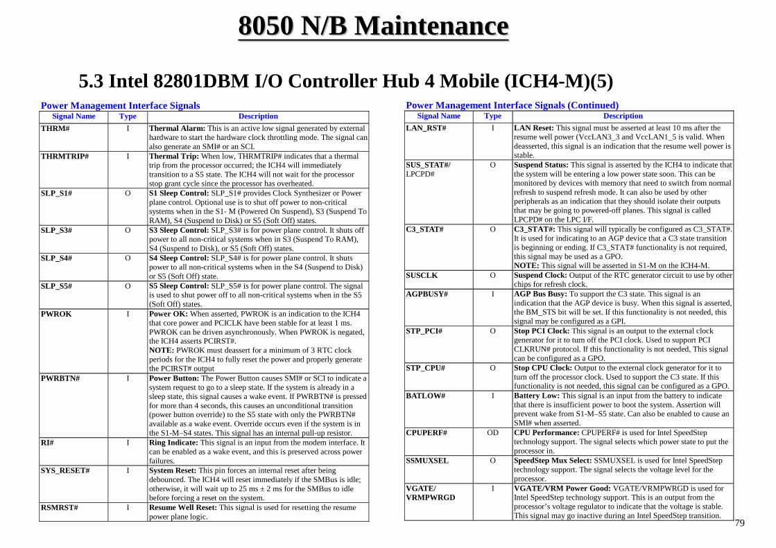
8050 8050 N/B MaintenanceN/B Maintenance
79
Power Management Interface Signals Signal Name Type Description
THRM# I Thermal Alarm: This is an active low signal generated by external hardware to start the hardware clock throttling mode. The signal can also generate an SMI# or an SCI.
THRMTRIP# I Thermal Trip: When low, THRMTRIP# indicates that a thermal trip from the processor occurred; the ICH4 will immediately transition to a S5 state. The ICH4 will not wait for the processor stop grant cycle since the processor has overheated.
SLP_S1# O S1 Sleep Control: SLP_S1# provides Clock Synthesizer or Power plane control. Optional use is to shut off power to non-critical systems when in the S1- M (Powered On Suspend), S3 (Suspend To RAM), S4 (Suspend to Disk) or S5 (Soft Off) states.
SLP_S3# O S3 Sleep Control: SLP_S3# is for power plane control. It shuts off power to all non-critical systems when in S3 (Suspend To RAM), S4 (Suspend to Disk), or S5 (Soft Off) states.
SLP_S4# O S4 Sleep Control: SLP_S4# is for power plane control. It shuts power to all non-critical systems when in the S4 (Suspend to Disk) or S5 (Soft Off) state.
SLP_S5# O S5 Sleep Control: SLP_S5# is for power plane control. The signal is used to shut power off to all non-critical systems when in the S5 (Soft Off) states.
PWROK I Power OK: When asserted, PWROK is an indication to the ICH4 that core power and PCICLK have been stable for at least 1 ms. PWROK can be driven asynchronously. When PWROK is negated, the ICH4 asserts PCIRST#. NOTE: PWROK must deassert for a minimum of 3 RTC clock periods for the ICH4 to fully reset the power and properly generate the PCIRST# output
PWRBTN# I Power Button: The Power Button causes SMI# or SCI to indicate a system request to go to a sleep state. If the system is already in a sleep state, this signal causes a wake event. If PWRBTN# is pressed for more than 4 seconds, this causes an unconditional transition (power button override) to the S5 state with only the PWRBTN# available as a wake event. Override occurs even if the system is in the S1-M–S4 states. This signal has an internal pull-up resistor.
RI# I Ring Indicate: This signal is an input from the modem interface. It can be enabled as a wake event, and this is preserved across power failures.
SYS_RESET# I System Reset: This pin forces an internal reset after being debounced. The ICH4 will reset immediately if the SMBus is idle; otherwise, it will wait up to 25 ms ± 2 ms for the SMBus to idle before forcing a reset on the system.
RSMRST# I Resume Well Reset: This signal is used for resetting the resume power plane logic.
Power Management Interface Signals (Continued)Signal Name Type Description
LAN_RST# I LAN Reset: This signal must be asserted at least 10 ms after the resume well power (VccLAN3_3 and VccLAN1_5 is valid. When deasserted, this signal is an indication that the resume well power is stable.
SUS_STAT#/ LPCPD#
O Suspend Status: This signal is asserted by the ICH4 to indicate that the system will be entering a low power state soon. This can be monitored by devices with memory that need to switch from normal refresh to suspend refresh mode. It can also be used by other peripherals as an indication that they should isolate their outputs that may be going to powered-off planes. This signal is called LPCPD# on the LPC I/F.
C3_STAT# O C3_STAT#: This signal will typically be configured as C3_STAT#. It is used for indicating to an AGP device that a C3 state transition is beginning or ending. If C3_STAT# functionality is not required, this signal may be used as a GPO. NOTE: This signal will be asserted in S1-M on the ICH4-M.
SUSCLK O Suspend Clock: Output of the RTC generator circuit to use by other chips for refresh clock.
AGPBUSY# I AGP Bus Busy: To support the C3 state. This signal is an indication that the AGP device is busy. When this signal is asserted, the BM_STS bit will be set. If this functionality is not needed, this signal may be configured as a GPI.
STP_PCI# O Stop PCI Clock: This signal is an output to the external clock generator for it to turn off the PCI clock. Used to support PCI CLKRUN# protocol. If this functionality is not needed, This signal can be configured as a GPO.
STP_CPU# O Stop CPU Clock: Output to the external clock generator for it to turn off the processor clock. Used to support the C3 state. If this functionality is not needed, this signal can be configured as a GPO.
BATLOW# I Battery Low: This signal is an input from the battery to indicate that there is insufficient power to boot the system. Assertion will prevent wake from S1-M–S5 state. Can also be enabled to cause an SMI# when asserted.
CPUPERF# OD CPU Performance: CPUPERF# is used for Intel SpeedStep technology support. The signal selects which power state to put the processor in.
SSMUXSEL O SpeedStep Mux Select: SSMUXSEL is used for Intel SpeedStep technology support. The signal selects the voltage level for the processor.
VGATE/ VRMPWRGD
I VGATE/VRM Power Good: VGATE/VRMPWRGD is used for Intel SpeedStep technology support. This is an output from the processor’s voltage regulator to indicate that the voltage is stable. This signal may go inactive during an Intel SpeedStep transition.
5.3 Intel 82801DBM I/O Controller Hub 4 Mobile (ICH4-M)(5)
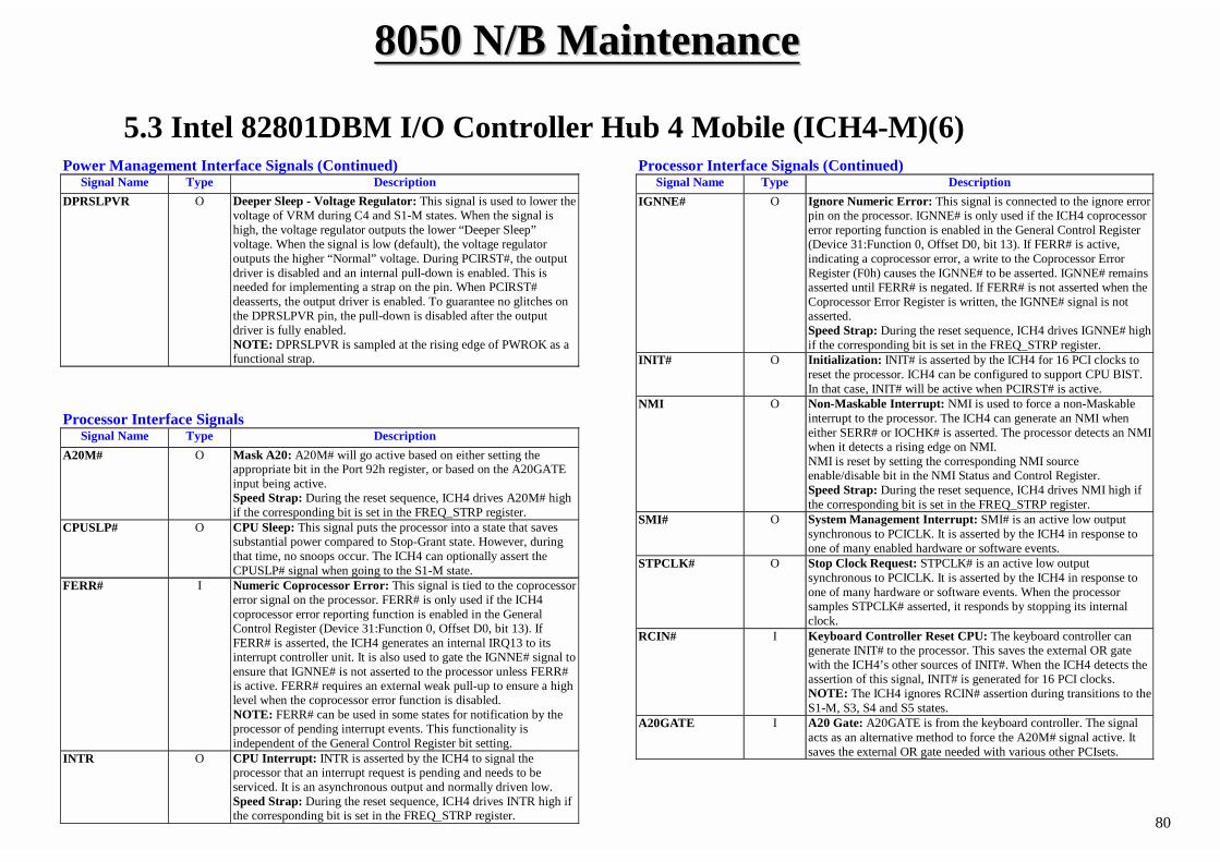
8050 8050 N/B MaintenanceN/B Maintenance
80
Power Management Interface Signals (Continued) Signal Name Type Description
DPRSLPVR O Deeper Sleep - Voltage Regulator: This signal is used to lower the voltage of VRM during C4 and S1-M states. When the signal is high, the voltage regulator outputs the lower “Deeper Sleep” voltage. When the signal is low (default), the voltage regulator outputs the higher “Normal” voltage. During PCIRST#, the output driver is disabled and an internal pull-down is enabled. This is needed for implementing a strap on the pin. When PCIRST# deasserts, the output driver is enabled. To guarantee no glitches on the DPRSLPVR pin, the pull-down is disabled after the output driver is fully enabled. NOTE: DPRSLPVR is sampled at the rising edge of PWROK as a functional strap.
Processor Interface Signals
Signal Name Type Description A20M# O Mask A20: A20M# will go active based on either setting the
appropriate bit in the Port 92h register, or based on the A20GATE input being active. Speed Strap: During the reset sequence, ICH4 drives A20M# high if the corresponding bit is set in the FREQ_STRP register.
CPUSLP# O CPU Sleep: This signal puts the processor into a state that saves substantial power compared to Stop-Grant state. However, during that time, no snoops occur. The ICH4 can optionally assert the CPUSLP# signal when going to the S1-M state.
FERR# I Numeric Coprocessor Error: This signal is tied to the coprocessor error signal on the processor. FERR# is only used if the ICH4 coprocessor error reporting function is enabled in the General Control Register (Device 31:Function 0, Offset D0, bit 13). If FERR# is asserted, the ICH4 generates an internal IRQ13 to its interrupt controller unit. It is also used to gate the IGNNE# signal to ensure that IGNNE# is not asserted to the processor unless FERR# is active. FERR# requires an external weak pull-up to ensure a high level when the coprocessor error function is disabled. NOTE: FERR# can be used in some states for notification by the processor of pending interrupt events. This functionality is independent of the General Control Register bit setting.
INTR O CPU Interrupt: INTR is asserted by the ICH4 to signal the processor that an interrupt request is pending and needs to be serviced. It is an asynchronous output and normally driven low. Speed Strap: During the reset sequence, ICH4 drives INTR high if the corresponding bit is set in the FREQ_STRP register.
Processor Interface Signals (Continued) Signal Name Type Description
IGNNE# O Ignore Numeric Error: This signal is connected to the ignore error pin on the processor. IGNNE# is only used if the ICH4 coprocessor error reporting function is enabled in the General Control Register (Device 31:Function 0, Offset D0, bit 13). If FERR# is active, indicating a coprocessor error, a write to the Coprocessor Error Register (F0h) causes the IGNNE# to be asserted. IGNNE# remains asserted until FERR# is negated. If FERR# is not asserted when the Coprocessor Error Register is written, the IGNNE# signal is not asserted. Speed Strap: During the reset sequence, ICH4 drives IGNNE# high if the corresponding bit is set in the FREQ_STRP register.
INIT# O Initialization: INIT# is asserted by the ICH4 for 16 PCI clocks to reset the processor. ICH4 can be configured to support CPU BIST. In that case, INIT# will be active when PCIRST# is active.
NMI O Non-Maskable Interrupt: NMI is used to force a non-Maskable interrupt to the processor. The ICH4 can generate an NMI when either SERR# or IOCHK# is asserted. The processor detects an NMI when it detects a rising edge on NMI. NMI is reset by setting the corresponding NMI source enable/disable bit in the NMI Status and Control Register. Speed Strap: During the reset sequence, ICH4 drives NMI high if the corresponding bit is set in the FREQ_STRP register.
SMI# O System Management Interrupt: SMI# is an active low output synchronous to PCICLK. It is asserted by the ICH4 in response to one of many enabled hardware or software events.
STPCLK# O Stop Clock Request: STPCLK# is an active low output synchronous to PCICLK. It is asserted by the ICH4 in response to one of many hardware or software events. When the processor samples STPCLK# asserted, it responds by stopping its internal clock.
RCIN# I Keyboard Controller Reset CPU: The keyboard controller can generate INIT# to the processor. This saves the external OR gate with the ICH4’s other sources of INIT#. When the ICH4 detects the assertion of this signal, INIT# is generated for 16 PCI clocks. NOTE: The ICH4 ignores RCIN# assertion during transitions to the S1-M, S3, S4 and S5 states.
A20GATE I A20 Gate: A20GATE is from the keyboard controller. The signal acts as an alternative method to force the A20M# signal active. It saves the external OR gate needed with various other PCIsets.
5.3 Intel 82801DBM I/O Controller Hub 4 Mobile (ICH4-M)(6)
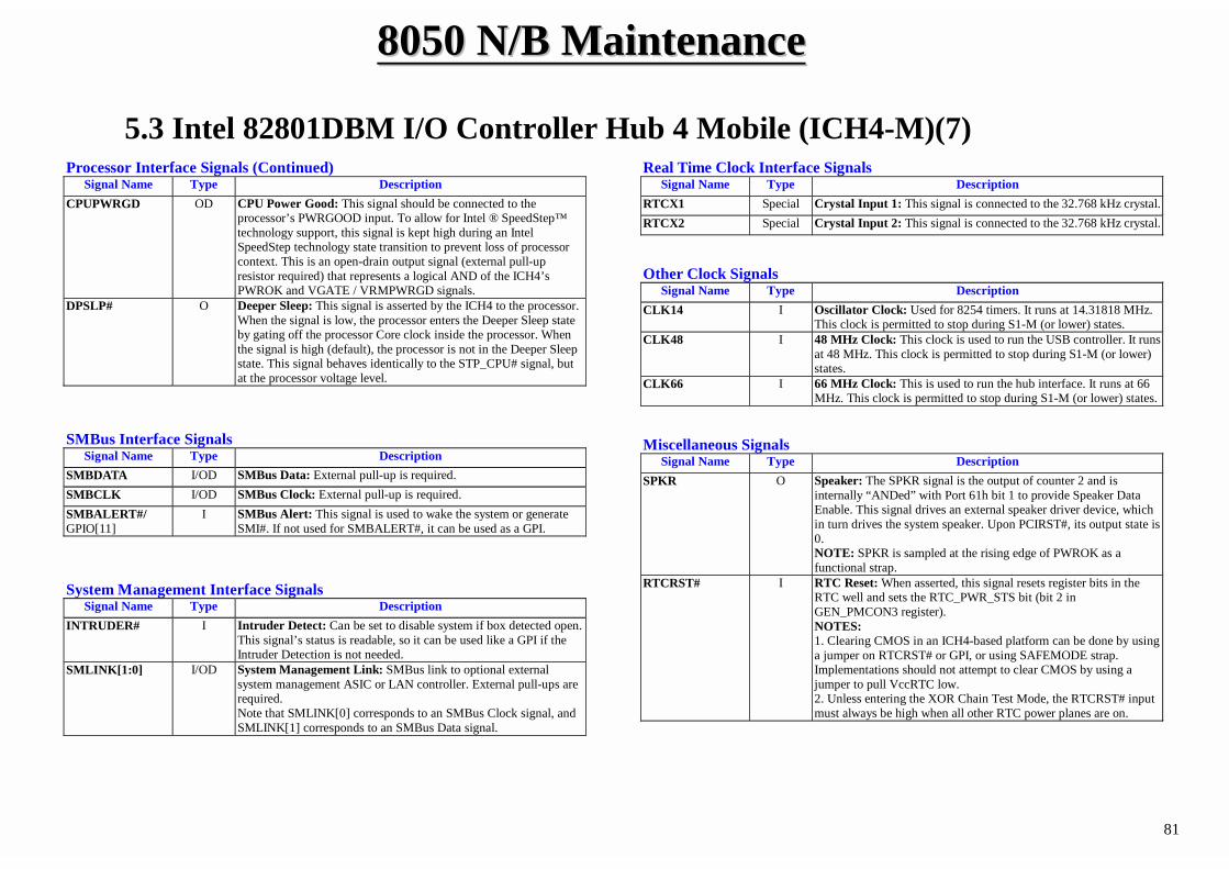
8050 8050 N/B MaintenanceN/B Maintenance
81
Processor Interface Signals (Continued) Signal Name Type Description
CPUPWRGD OD CPU Power Good: This signal should be connected to the processor’s PWRGOOD input. To allow for Intel ® SpeedStep™ technology support, this signal is kept high during an Intel SpeedStep technology state transition to prevent loss of processor context. This is an open-drain output signal (external pull-up resistor required) that represents a logical AND of the ICH4’s PWROK and VGATE / VRMPWRGD signals.
DPSLP# O Deeper Sleep: This signal is asserted by the ICH4 to the processor. When the signal is low, the processor enters the Deeper Sleep state by gating off the processor Core clock inside the processor. When the signal is high (default), the processor is not in the Deeper Sleep state. This signal behaves identically to the STP_CPU# signal, but at the processor voltage level.
SMBus Interface Signals
Signal Name Type Description SMBDATA I/OD SMBus Data: External pull-up is required. SMBCLK I/OD SMBus Clock: External pull-up is required. SMBALERT#/ GPIO[11]
I SMBus Alert: This signal is used to wake the system or generate SMI#. If not used for SMBALERT#, it can be used as a GPI.
System Management Interface Signals
Signal Name Type Description INTRUDER# I Intruder Detect: Can be set to disable system if box detected open.
This signal’s status is readable, so it can be used like a GPI if the Intruder Detection is not needed.
SMLINK[1:0] I/OD System Management Link: SMBus link to optional external system management ASIC or LAN controller. External pull-ups are required. Note that SMLINK[0] corresponds to an SMBus Clock signal, and SMLINK[1] corresponds to an SMBus Data signal.
Real Time Clock Interface Signals Signal Name Type Description
RTCX1 Special Crystal Input 1: This signal is connected to the 32.768 kHz crystal. RTCX2 Special Crystal Input 2: This signal is connected to the 32.768 kHz crystal. Other Clock Signals
Signal Name Type Description CLK14 I Oscillator Clock: Used for 8254 timers. It runs at 14.31818 MHz.
This clock is permitted to stop during S1-M (or lower) states. CLK48 I 48 MHz Clock: This clock is used to run the USB controller. It runs
at 48 MHz. This clock is permitted to stop during S1-M (or lower) states.
CLK66 I 66 MHz Clock: This is used to run the hub interface. It runs at 66 MHz. This clock is permitted to stop during S1-M (or lower) states.
Miscellaneous Signals
Signal Name Type Description SPKR O Speaker: The SPKR signal is the output of counter 2 and is
internally “ANDed” with Port 61h bit 1 to provide Speaker Data Enable. This signal drives an external speaker driver device, which in turn drives the system speaker. Upon PCIRST#, its output state is 0. NOTE: SPKR is sampled at the rising edge of PWROK as a functional strap.
RTCRST# I RTC Reset: When asserted, this signal resets register bits in the RTC well and sets the RTC_PWR_STS bit (bit 2 in GEN_PMCON3 register). NOTES: 1. Clearing CMOS in an ICH4-based platform can be done by using a jumper on RTCRST# or GPI, or using SAFEMODE strap. Implementations should not attempt to clear CMOS by using a jumper to pull VccRTC low. 2. Unless entering the XOR Chain Test Mode, the RTCRST# input must always be high when all other RTC power planes are on.
5.3 Intel 82801DBM I/O Controller Hub 4 Mobile (ICH4-M)(7)
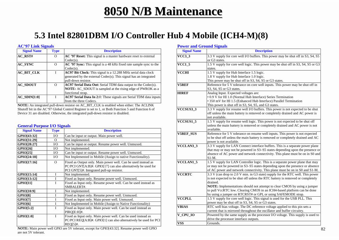
8050 8050 N/B MaintenanceN/B Maintenance
82
AC’97 Link Signals Signal Name Type Description
AC_RST# O AC ’97 Reset: This signal is a master hardware reset to external Codec(s).
AC_SYNC O AC ’97 Sync: This signal is a 48 kHz fixed rate sample sync to the Codec(s).
AC_BIT_CLK I AC97 Bit Clock: This signal is a 12.288 MHz serial data clock generated by the external Codec(s). This signal has an integrated pull-down resistor.
AC_SDOUT O AC97 Serial Data Out: Serial TDM data output to the Codec(s). NOTE: AC_SDOUT is sampled at the rising edge of PWROK as a functional strap.
AC_SDIN[1:0] I AC97 Serial Data In 2:0: These signals are Serial TDM data inputs from the three Codecs.
NOTE: An integrated pull-down resistor on AC_BIT_CLK is enabled when either: The ACLINK Shutoff bit in the AC’97 Global Control Register is set to 1, or Both Function 5 and Function 6 of Device 31 are disabled. Otherwise, the integrated pull-down resistor is disabled. General Purpose I/O Signals
Signal Name Type Description GPIO[43:32] I/O Can be input or output. Main power well. GPIO[31:29] O Not implemented. GPIO[28:27] I/O Can be input or output. Resume power well. Unmuxed. GPIO[26] I/O Not implemented. GPIO[25] I/O Can be input or output. Resume power well. Unmuxed. GPIO[24:18] I/O Not Implemented in Mobile (Assign to native Functionality). GPIO[17:16] O Fixed as Output only. Main power well. Can be used instead as
PC/PCI GNT[A:B]#. GPIO[17] can also alternatively be used for PCI GNT[5]#. Integrated pull-up resistor.
GPIO[15:14] I Not implemented. GPIO[13:12] I Fixed as Input only. Resume power well. Unmuxed. GPIO[11] I Fixed as Input only. Resume power well. Can be used instead as
SMBALERT#. GPIO[10:9] I Not implemented. GPIO[8] I Fixed as Input only. Resume power well. Unmuxed. GPIO[7] I Fixed as Input only. Main power well. Unmuxed. GPIO[6] I Not Implemented in Mobile (Assign to Native Functionality) GPIO[5:2] I Fixed as Input only. Main power well. Can be used instead as
PIRQ[E:H]#. GPIO[1:0] I Fixed as Input only. Main power well. Can be used instead as
PC/PCI REQ[A:B]#. GPIO[1] can also alternatively be used for PCI REQ[5]#.
NOTE: Main power well GPIO are 5V tolerant, except for GPIO[43:32]. Resume power well GPIO are not 5V tolerant.
Power and Ground Signals Signal Name Description
VCC3_3 3.3 V supply for core well I/O buffers. This power may be shut off in S3, S4, S5 or G3 states.
VCC1_5 1.5 V supply for core well logic. This power may be shut off in S3, S4, S5 or G3 states.
VCCHI 1.5 V supply for Hub Interface 1.5 logic. 1.8 V supply for Hub Interface 1.0 logic. This power may be shut off in S3, S4, S5 or G3 states.
V5REF Reference for 5 V tolerance on core well inputs. This power may be shut off in S3, S4, S5 or G3 states.
HIREF Analog Input. Expected voltages are: • 0.9 V for HI 1.0 (Normal Hub Interface) Series Termination • 350 mV for HI 1.5 (Enhanced Hub Interface) Parallel Termination This power is shut off in S3, S4, S5, and G3 states.
VCCSUS3_3 3.3 V supply for resume well I/O buffers. This power is not expected to be shut off unless the main battery is removed or completely drained and AC power is not available.
VCCSUS1_5 1.5 V supply for resume well logic. This power is not expected to be shut off unless the main battery is removed or completely drained and AC power is not available.
V5REF_SUS Reference for 5 V tolerance on resume well inputs. This power is not expected to be shut off unless the main battery is removed or completely drained and AC power is not available.
VCCLAN3_3 3.3 V supply for LAN Connect interface buffers. This is a separate power plane that may or may not be powered in S3–S5 states depending upon the presence or absence of AC power and network connectivity. This plane must be on in S0 and S1-M.
VCCLAN1_5 1.5 V supply for LAN Controller logic. This is a separate power plane that may or may not be powered in S3–S5 states depending upon the presence or absence of AC power and network connectivity. This plane must be on in S0 and S1-M.
VCCRTC 3.3 V (can drop to 2.0 V min. in G3 state) supply for the RTC well. This power is not expected to be shut off unless the RTC battery is removed or completely drained. NOTE: Implementations should not attempt to clear CMOS by using a jumper to pull VccRTC low. Clearing CMOS in an ICH4-based platform can be done by using a jumper on RTCRST# or GPI, or using SAFEMODE strap.
VCCPLL 1.5 V supply for core well logic. This signal is used for the USB PLL. This power may be shut off in S3, S4, S5 or G3 states.
VBIAS RTC well bias voltage. The DC reference voltage applied to this pin sets a current that is mirrored throughout the oscillator and buffer circuitry.
V_CPU_IO Powered by the same supply as the processor I/O voltage. This supply is used to drive the processor interface outputs.
VSS Grounds.
5.3 Intel 82801DBM I/O Controller Hub 4 Mobile (ICH4-M)(8)
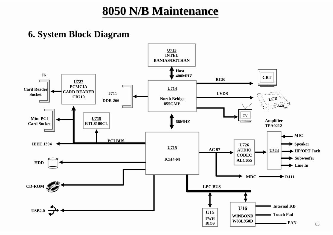
8050 8050 N/B MaintenanceN/B Maintenance
83
U713INTEL
BANIAS/DOTHAN
U714
North Bridge855GME
Internal KB
Touch PadU16
WINBONDW83L950D
U726AUDIOCODECALC655
MIC
Line In
Card Reader Socket
PCI BUS
LPC BUS
J711
DDR 266
AC 97 U524
AmplifierTPA0212
U15FWHBIOS
HDD
USB2.0
CD-ROM
U715
ICH4-M
MDC RJ11
FAN
U727PCMCIA
CARD READERCB710 LCDLCD
CRTRGB
LVDS
66MHZ
Speaker
J6
Mini PCI Card Socket
TV
HP/OPT Jack
Subwoofer
IEEE 1394
U719RTL8100CL
Host400MHZ
6. System Block Diagram
8050 8050 N/B MaintenanceN/B Maintenance
84
7.1 Introduction
Each time the computer is turned on, the system BIOS runs a series of internal checks on the hardware. This power-on self test (post) allows the computer to detect problems as early as the power-on stage. Error messages of post can alert you to the problems of your computer.If an error is detected during these tests, you will see an error message displayed on the screen. If the error occurs before the display is initialized, then the screen cannot display the error message. Error codes or system beeps are used to identify a post error that occurs when the screen is not available.
The value for the diagnostic port is written at the beginning of the test. Therefore, if the test failed, the user can determine where the problem occurred by reading the last value written to the port by the debug card plug at MINI PCI slot.
7. Maintenance Diagnostics
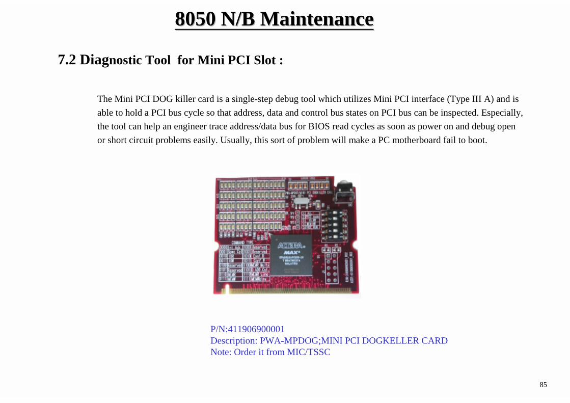
8050 8050 N/B MaintenanceN/B Maintenance
85
The Mini PCI DOG killer card is a single-step debug tool which utilizes Mini PCI interface (Type III A) and is able to hold a PCI bus cycle so that address, data and control bus states on PCI bus can be inspected. Especially, the tool can help an engineer trace address/data bus for BIOS read cycles as soon as power on and debug open or short circuit problems easily. Usually, this sort of problem will make a PC motherboard fail to boot.
P/N:411906900001Description: PWA-MPDOG;MINI PCI DOGKELLER CARDNote: Order it from MIC/TSSC
7.2 Diagnostic Tool for Mini PCI Slot :
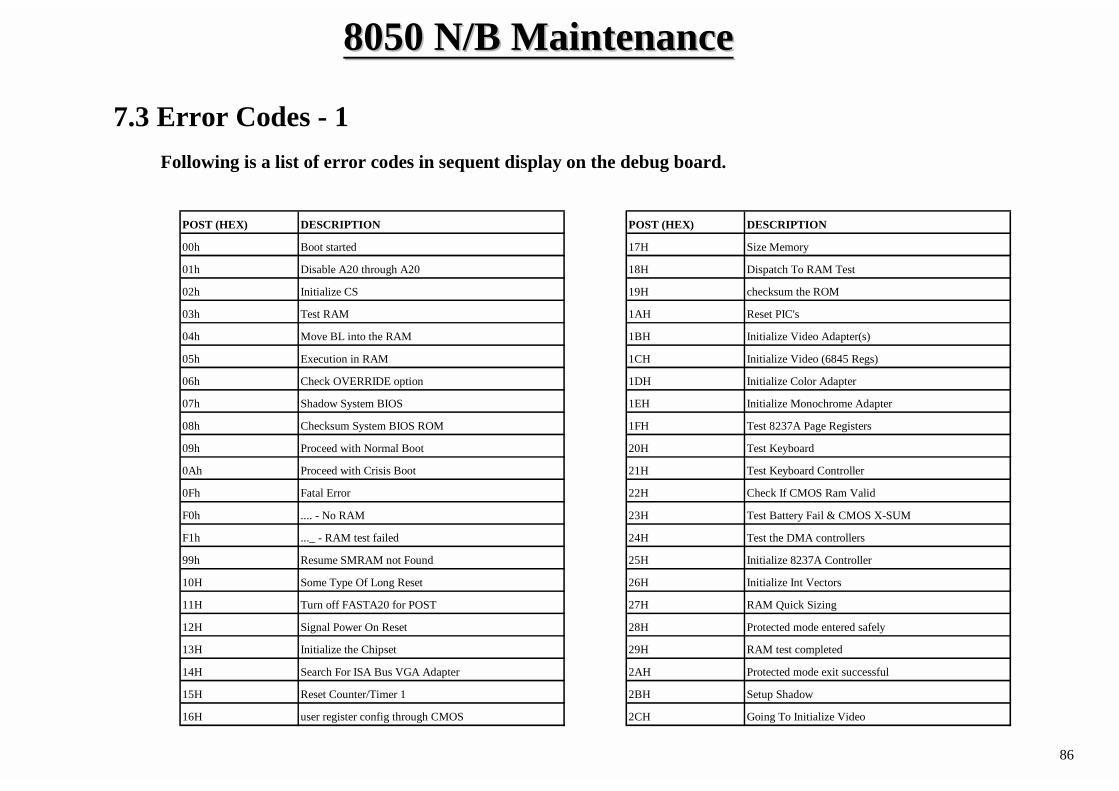
8050 8050 N/B MaintenanceN/B Maintenance
86
Following is a list of error codes in sequent display on the debug board.
POST (HEX) DESCRIPTION
17H Size Memory
18H Dispatch To RAM Test
19H checksum the ROM
1AH Reset PIC's
1BH Initialize Video Adapter(s)
1CH Initialize Video (6845 Regs)
1DH Initialize Color Adapter
1EH Initialize Monochrome Adapter
1FH Test 8237A Page Registers
20H Test Keyboard
21H Test Keyboard Controller
22H Check If CMOS Ram Valid
23H Test Battery Fail & CMOS X-SUM
24H Test the DMA controllers
25H Initialize 8237A Controller
26H Initialize Int Vectors
27H RAM Quick Sizing
28H Protected mode entered safely
29H RAM test completed
2AH Protected mode exit successful
2BH Setup Shadow
2CH Going To Initialize Video
POST (HEX) DESCRIPTION
00h Boot started
01h Disable A20 through A20
02h Initialize CS
03h Test RAM
04h Move BL into the RAM
05h Execution in RAM
06h Check OVERRIDE option
07h Shadow System BIOS
08h Checksum System BIOS ROM
09h Proceed with Normal Boot
0Ah Proceed with Crisis Boot
0Fh Fatal Error
F0h .... - No RAM
F1h ..._ - RAM test failed
99h Resume SMRAM not Found
10H Some Type Of Long Reset
11H Turn off FASTA20 for POST
12H Signal Power On Reset
13H Initialize the Chipset
14H Search For ISA Bus VGA Adapter
15H Reset Counter/Timer 1
16H user register config through CMOS
7.3 Error Codes - 1
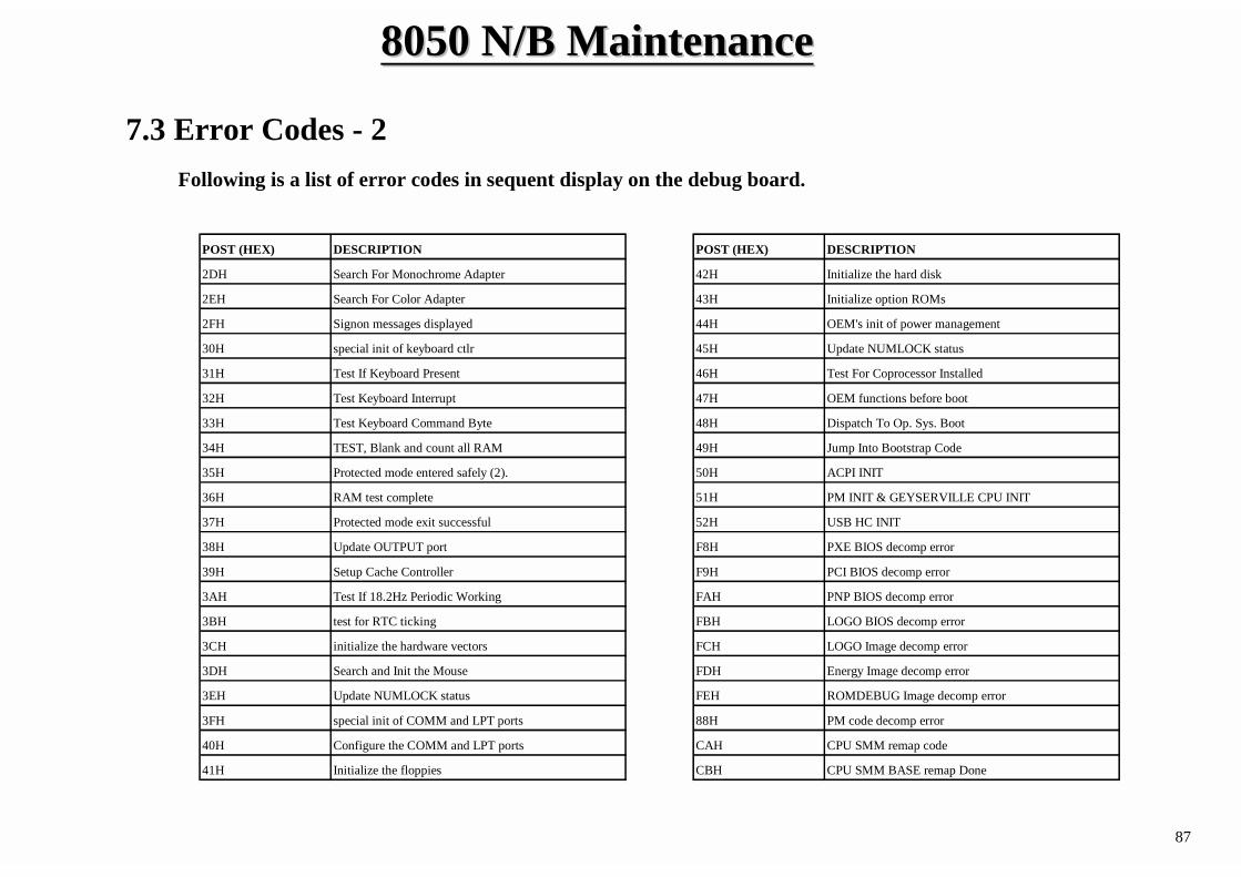
8050 8050 N/B MaintenanceN/B Maintenance
87
POST (HEX) DESCRIPTION
2DH Search For Monochrome Adapter
2EH Search For Color Adapter
2FH Signon messages displayed
30H special init of keyboard ctlr
31H Test If Keyboard Present
32H Test Keyboard Interrupt
33H Test Keyboard Command Byte
34H TEST, Blank and count all RAM
35H Protected mode entered safely (2).
36H RAM test complete
37H Protected mode exit successful
38H Update OUTPUT port
39H Setup Cache Controller
3AH Test If 18.2Hz Periodic Working
3BH test for RTC ticking
3CH initialize the hardware vectors
3DH Search and Init the Mouse
3EH Update NUMLOCK status
3FH special init of COMM and LPT ports
40H Configure the COMM and LPT ports
41H Initialize the floppies
POST (HEX) DESCRIPTION
42H Initialize the hard disk
43H Initialize option ROMs
44H OEM's init of power management
45H Update NUMLOCK status
46H Test For Coprocessor Installed
47H OEM functions before boot
48H Dispatch To Op. Sys. Boot
49H Jump Into Bootstrap Code
50H ACPI INIT
51H PM INIT & GEYSERVILLE CPU INIT
52H USB HC INIT
F8H PXE BIOS decomp error
F9H PCI BIOS decomp error
FAH PNP BIOS decomp error
FBH LOGO BIOS decomp error
FCH LOGO Image decomp error
FDH Energy Image decomp error
FEH ROMDEBUG Image decomp error
88H PM code decomp error
CAH CPU SMM remap code
CBH CPU SMM BASE remap Done
7.3 Error Codes - 2Following is a list of error codes in sequent display on the debug board.
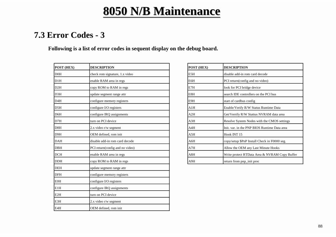
8050 8050 N/B MaintenanceN/B Maintenance
88
POST (HEX) DESCRIPTION
D0H check rom signature, 1.x video
D1H enable RAM area in regs
D2H copy ROM to RAM in regs
D3H update segment range attr
D4H configure memory registers
D5H configure I/O registers
D6H configure IRQ assignments
D7H turn on PCI device
D8H 2.x video r/w segment
D9H OEM defined, rom init
DAH disable add-in rom card decode
DBH PCI return(config and no video)
DCH enable RAM area in regs
DDH copy ROM to RAM in regs
DEH update segment range attr
DFH configure memory registers
E0H configure I/O registers
E1H configure IRQ assignments
E2H turn on PCI device
E3H 2.x video r/w segment
E4H OEM defined, rom init
POST (HEX) DESCRIPTION
E5H disable add-in rom card decode
E6H PCI return(config and no video)
E7H look for PCI bridge device
E8H search IDE controllers on the PCI bus
E9H start of cardbus config
A1H Enable/Verify R/W Status Runtime Data
A2H Get/Verrify R/W Stattus NVRAM data area
A3H Resolve System Nodes with the CMOS settings
A4H Init. var. in the PNP BIOS Runtime Data area
A5H Hook INT 15
A6H copy/setup $PnP Install Check in F0000 seg.
A7H Allow the OEM any Last Minute Hooks
A8H Write protect RTData Area & NVRAM Copy Buffer
A9H return from pnp_init proc
7.3 Error Codes - 3Following is a list of error codes in sequent display on the debug board.
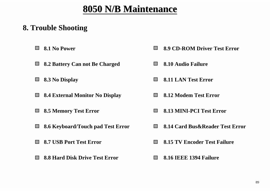
8050 8050 N/B MaintenanceN/B Maintenance
89
8.1 No Power
8.3 No Display
8.2 Battery Can not Be Charged
8.4 External Monitor No Display
8.5 Memory Test Error
8.6 Keyboard/Touch pad Test Error
8.7 USB Port Test Error
8.9 CD-ROM Driver Test Error
8.10 Audio Failure
8.11 LAN Test Error
8.12 Modem Test Error
8.13 MINI-PCI Test Error
8.14 Card Bus&Reader Test Error
8.16 IEEE 1394 Failure
8.15 TV Encoder Test Failure
8.8 Hard Disk Drive Test Error
8. Trouble Shooting
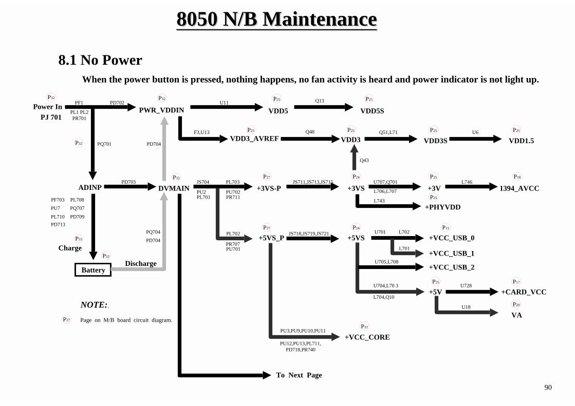
8050 8050 N/B MaintenanceN/B Maintenance
90
When the power button is pressed, nothing happens, no fan activity is heard and power indicator is not light up.
Power InPJ 701
PWR_VDDIN VDD5 VDD5SPD702PF1
PL1 PL2 PR701
U11 Q13
PQ701
ADINP DVMAIN
Battery
Charge
+3VS-P +3VS
+5VS_P
PD703 JS704
PU702PL701PU2
PU701
P32 P32 P25
P24
P25
P27P32
P32
P27PD713
PF703PU7
PL710
+5VSP24
U701P15
+VCC_USB_0
U704,L70 3
L704,Q10
P25
+5VU728
+CARD_VCCP17
To Next Page
Page on M/B board circuit diagram.P27
NOTE:.
PD704VDD3 VDD3S VDD1.5
U6F3,U13
+3VU707,Q701
L706,L707
P25 P25 P25
P25
Q51,L71
PR711
PR707
JS711,JS713,JS715
JS718,JS719,JS721P33
PL708
PD709
PL703
PL702
PQ707
P32
PQ704PD704
Discharge
VDD3_AVREF
8.1 No Power
P25 Q48
L702
L701+VCC_USB_1
+VCC_USB_2U705,L708
1394_AVCC
+PHYVDDP25
P18
L743
L746
U18
VAP20
+VCC_COREP31
PU3,PU9,PU10,PU11
PU12,PU13,PL711,PD718,PR740
Q43
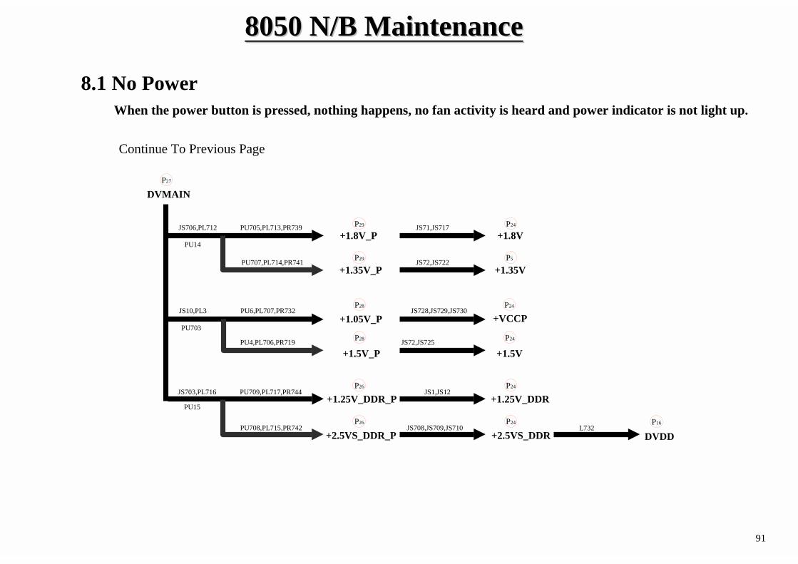
8050 8050 N/B MaintenanceN/B Maintenance
91
P27
+1.25V_DDR
+1.8V
+1.35V
+1.25V_DDR_P
+1.8V_P
+1.35V_PPU707,PL714,PR741
PU709,PL717,PR744
P29
P29 P24
P5
P26 P24
PU705,PL713,PR739
Continue To Previous Page
DVMAIN
JS71,JS717
JS1,JS12
JS72,JS722
JS706,PL712
When the power button is pressed, nothing happens, no fan activity is heard and power indicator is not light up.
8.1 No Power
JS708,JS709,JS710+2.5VS_DDR_P
PU708,PL715,PR742
P24P26JS703,PL716
+2.5VS_DDR
PU14
PU15
DVDDP16
L732
PU6,PL707,PR732+1.05V_P
P28
+VCCPP24
JS728,JS729,JS730
PU703
+1.5V_PPU4,PL706,PR719 P28 P24JS72,JS725
JS10,PL3
+1.5V
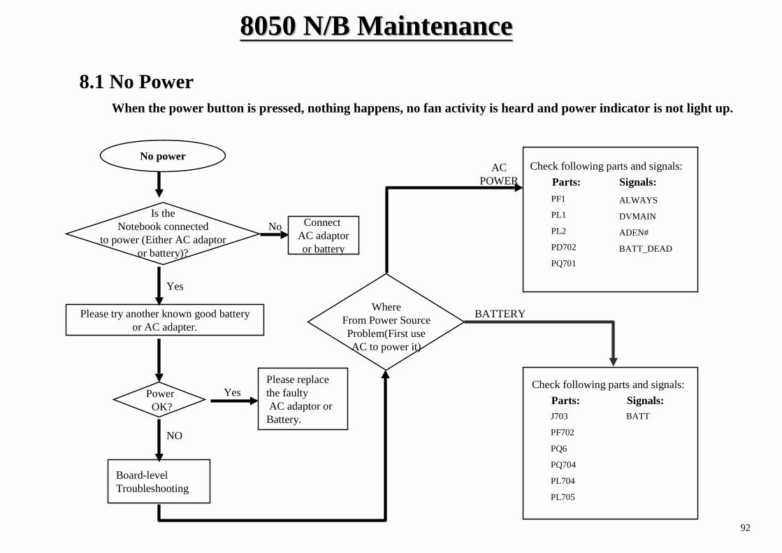
8050 8050 N/B MaintenanceN/B Maintenance
92
No power
Connect AC adaptoror battery
Please replace the faultyAC adaptor or
Battery.
PowerOK?
Yes
No
Please try another known good batteryor AC adapter.
Yes
Is theNotebook connected
to power (Either AC adaptoror battery)?
NO
Board-levelTroubleshooting
WhereFrom Power SourceProblem(First useAC to power it)
Check following parts and signals:Parts: Signals:
ALWAYS
DVMAIN
ADEN#
BATT_DEAD
PF1
PL1
PL2
PD702
PQ701
Check following parts and signals:Parts: Signals:J703
PF702
PQ6
PQ704
PL704
PL705
BATT
AC POWER
BATTERY
8.1 No PowerWhen the power button is pressed, nothing happens, no fan activity is heard and power indicator is not light up.
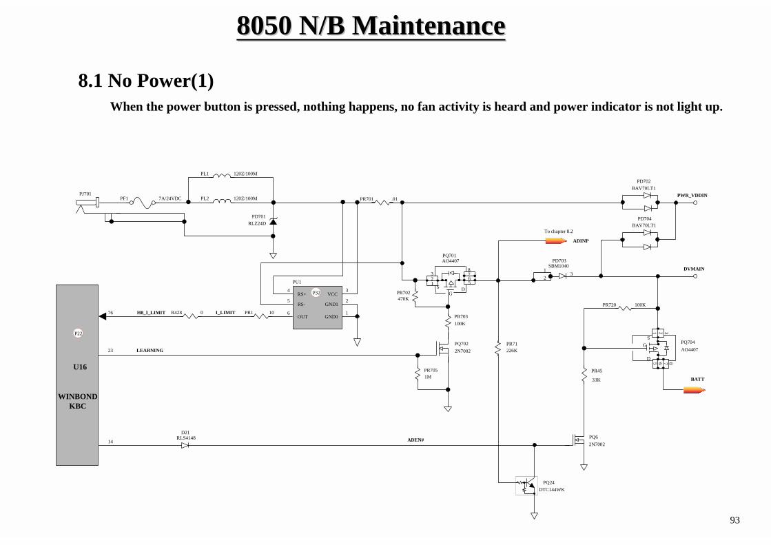
8050 8050 N/B MaintenanceN/B Maintenance
93
G
S
D
2 316 7 85
PJ701PF1 PL2 PR701
PD703
PD702
PD704
G
S
D
23
1678
5
PQ701
PD701
DVMAIN
PQ704
PR720
PR45
PQ6
PQ24
LEARNING
ADINP
PWR_VDDIN
BATT
ADEN#
I_LIMIT PR1R428H8_I_LIMIT
U16
7A/24VDC
120Z/100M
120Z/100M
RLZ24D
.01
RS+
RS-
OUT
VCC
GND1
GND0
PU1
4
5
6
AO4407
PR702470K
PR703
BAV70LT1
BAV70LT1
SBM1040
100K
AO4407
33K
2N7002
PR71226K
DTC144WK
10076
23PQ702
D21
100K
2N7002
1M
RLS4148
PL1
WINBOND KBC
PR705
14
3
2
1
P22
P32
321
To chapter 8.2
8.1 No Power(1)When the power button is pressed, nothing happens, no fan activity is heard and power indicator is not light up.
8050 8050 N/B MaintenanceN/B Maintenance
94
PR23
PR24
PR20
PWR_VDDIN
VDD3
VDD3S
J703
6
5
4
3
2
1
7
PF702 PL705
U16
WINBOND KBC
0
0
PD2BAV99
PD3BAV99
78
77
2
3
BAT_V
BAT_C
BAT_D
BAT_T
120Z/100M
PR716499K
PL704120Z/100M
4.99K
7A/24VDC
1
2
3
45
6
7
8
22*4RP45
4
678
23
15
14 ADEN#PQ6
2N7002
D21RLS4148
PR4533K
PR720100K
DVMAIN
PD704BAV70LT1
P32
BA
TTCO
NN
ECTOR
P22
BATT
PQ704AO4407
PC7220.01U
PR714100K
8.1 No Power(2)When the power button is pressed, nothing happens, no fan activity is heard and power indicator is not light up.

8050 8050 N/B MaintenanceN/B Maintenance
95
Battery can not Charge
Connect AC adaptor.
No
Yes
No
Yes
Is thenotebook connected
to power (AC adaptor)?
1. Make sure that the battery is good.2. Make sure that the battery is installed properly.
Please replace the faulty Battery.
Battery chargeOK?
Check following parts and signals:
Parts Signal
PF703PL708PQ707PL710PD713PD714PD709PQ13PQ14PU7PQ15PD5PR65
ADINPCHANGING BATTBAT_VBAT_T BAT_C BAT_D BATT_DEADI_CTRL
Board-levelTroubleshooting
ReplaceMotherboard
PR70PQ11PC33PR63PU5PR74PR75PR76PQ12
8.2 Battery Can not Be ChargedThere are problems in charging the battery.
8050 8050 N/B MaintenanceN/B Maintenance
96
G
S
D
23
1678
5
C1
ADINP
PR86
PC39
BATT
PR74
PR76
CHARGING
21N+
CHARGING
PF703TR/3216FF-3A
PL708BEAD_120Z/100M
0
PQ13DTA144WK
PQ142N7002
U16
WINBOND KBC
8C2
VCC 21IN+
PU7
11
12 16
PD713EC31QS04
PL7093.0UH
PQ707AO4407
PR79 124K
PR780
PR874.7K
PR884.7K
PR89100KPQ15
MMBT2222A
PD5BAS32L
PD714EC31QS04
33UHPL710
R483 0
26
10 I_CTRL
78
77
BAT_V
BAT_T
BAT_C
BAT_D
2
3
15
2
13.7K
249K
PD709BZV55C15V
PQ122N7002
1000PPR7520K
P33P22
TL594C
From U16
From chapter 8.1(1)
PC48 0.01U
13
BATT_DEAD#
-
DVMAIN VDD5
PR70PR65
+
PU5
5
6
8
7
4
BATT_DEAD=8.56V
PR69100K 590K 3.3K
LMV393M
DTC144TKAQ39
1.25V
PQ11SCK431LCSK-.5
PC330.1U
PR6380.6K
PC360.01U
Reference chapter 8.1(1)
8.2 Battery Can not Be Charged
Reference chapter 8.1(2)
There are problems in charging the battery.
8050 8050 N/B MaintenanceN/B Maintenance
97
Replace monitoror LCD. Board-level
Troubleshooting
Yes
NoMonitoror LCD module
OK?
Make sure that CPU module,DIMM memory are installedProperly.
DisplayOK?
Yes
No
Correct it.Using debug card,depending on the error codes to make sure which parts maybe faulty
ReplaceMotherboard
1.Try another known good CPU module, DIMM module and BIOS.
2.Remove all of I/O device (FDD,HDD, CD-ROM…….) frommotherboard except LCD or monitor.
DisplayOK?
1. Replace faulty part.2. Connect the I/O device to the
M/B one at a time to find outwhich part is causing the problem.
Yes
No
No Display
8.3 No Display
Using circuit diagram ,check the faulty parts
There is no display on both LCD and VGA monitor after power on although the LCD and monitor is known-good.
8050 8050 N/B MaintenanceN/B Maintenance
98
****** System Clock Check ******
U726
U713
R874 R87544,45
U714
35,3848,49
R865 R872R873 R878
J713
U715
R895 R1137 MINIPCI_SIO48M39
R877
R81611
USBCLK_ICH
R824 PCICLK_ICH
R858
R859 R472 14M_CODEC
7
56
12 R826
U727
U719R82713 PCICLK_LAN
PCICLK_CARD
48M_DREFCLK66M_DEFSSCLK
HCLK_MCHHCLK_MCH#
PCICLK_MINIPCI
14M_ICH
U712
ClockGenerator
ICS950810
29,30 SMBDATASMBCLK
R821
+3V
R831
28VTT_PWRGD#
R828
U724PCICLK_139416
U1510 R825 PCICLK_FWH
U1617 R817 PCICK_KBC
2
3
X70314.318MHZ
CPU
NB
MINI
ICH4_M
R860+3V 54
55
40
4.7K
FS2
R863
L722 CLKANA
L726
L43
L718
+3V
CLK66
CLKCPU
CLKPCI 8,14
43
19,32
46,50
1,26,37
8.2K
120Z/100M
120Z/100M
120Z/100M
120Z/100M
10K
0CORE_CLKEN#
PR560
PR7312K
+3V
PR57 0
PR591M
2N7002PQ8
VCCP_PWRGD
PR715100K
PR717 0 27PU703
+3VS_P
33*2 HCLK_CPU HCLK_CPU#
33*4
33
0
J711
33
33
33
33
33 0
33
33
33
33
33
FS1
FS0
P11
P28
P19
P13
P20
P17
P16
P18
P23
P22
P2 P3
P4 P5
P14
AUDIO
P6
LTC3728L
CARDBUS
LAN
DDR
KBC
SYS
IEEE
READER
CODEC
SODIMM
1394
BIOS
WINBOND
-PCI
C804 C79427P 27P
8.3 No Display(1)
R863 4.7K
R894 4.7K
001
FS2 FS1 FS0 CPU
0 1x 100.00
0:001:3.3V
UNIT:MHZ
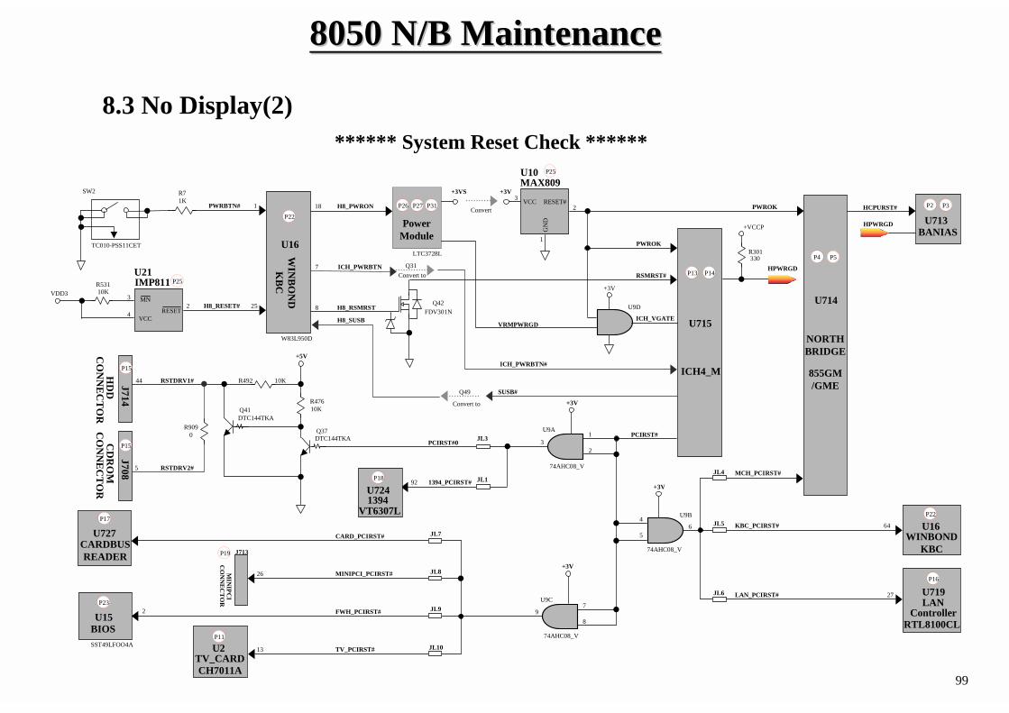
8050 8050 N/B MaintenanceN/B Maintenance
99
****** System Reset Check ******
IMP811
PCIRST#
RSTDRV1#
U714
855GM/GME
U715
ICH4_M
RESET#VCC
GN
D
PWROK
1
2H8_PWRON
Power Module
H8_RSMRSTQ42
FDV301N
RSMRST#
+3VS3
+5V
R492
R476
Q37
Q41DTC144TKA
DTC144TKA
10K
10K
J714H
DD
44
1394_PCIRST#
PCIRST#0
92U724
VT6307L
MCH_PCIRST#
KBC_PCIRST# 64 U16WINBOND
KBC
U719LAN_PCIRST# 27
RTL8100CL
CARD_PCIRST#U727CARDBUSREADER
+3V
+3V
MINIPCI_PCIRST#26
J713
FWH_PCIRST#U152
SST49LFOO4ATV_PCIRST#U2 13
CH7011A
U21R531
VDD3
25
SW2 R7
PWRBTN# 11K
H8_RESET#
W83L950D
U16
10KMN
VCC
18
823
4 RESET
HCPURST#
BANIASU713
PWROK
CO
NN
EC
TO
R
MIN
IPCI
CO
NN
EC
TO
R
74AHC08_V
U9A
U9B
74AHC08_V
U9C
74AHC08_V
1
23
4
56
7
89
TC010-PSS11CET
P14P13
P22
P25
P15
P17
P19
P11
P18
P16
P22
P2 P3
P5P4
P27
LTC3728L
P25U10MAX809
NORTHBRIDGE
WIN
BO
ND
KB
C
P23
1394
BIOS
TV_CARD
LANController
+VCCP
R301330
HPWRGD
HPWRGD
VRMPWRGD
U9D
ICH_VGATE
+3V
+3V
ConvertP26 P31
ICH_PWRBTN
ICH_PWRBTN#
H8_SUSB
SUSB#
JL3
JL1
R909 0
J708
8.3 No Display(2)
7Convert to
Q31
+3V
Convert to
Q49
P15
CD
RO
MC
ON
NE
CT
OR
RSTDRV2#5
JL7
JL8
JL9
JL4
JL5
JL6
JL10
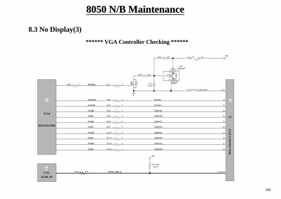
8050 8050 N/B MaintenanceN/B Maintenance
100
****** VGA Controller Checking ******
J2U714
855GM/GME
FPVDENR801 0 R22 0
R19 10K G
S
D
2 316 7 85
R16 1M
C140.22U
F1 2A+3V
L15 120Z/100M 1,2,3
TXCLK+
U715ICH4_M
TXCLK-ICLKAM
ICLKAP
R361
0R363
0
IYAM0
R350 0
R349 0
IYAP0
TXOUT0-
TXOUT0+
IYAM1
R357 0
R353 0
IYAP1
TXOUT1-
TXOUT1+
IYAM2
R1177 0
R1176 0
IYAP2
TXOUT2-
TXOUT2+
IYAM3
R1179 0
0
IYAP3
TXOUT3-
TXOUT3+
R1178
19
21
25
27
20
22
26
28
13
15
PANEL_ID[0..3] 6,7,10,14
+3V
R11~R1410K*4
RP26 0*4
LC
D C
ON
NE
CT
OR
P14
P5 P12
Q9SI4835DY
8.3 No Display(3)
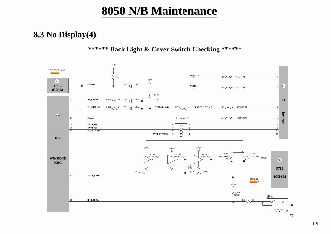
8050 8050 N/B MaintenanceN/B Maintenance
101
****** Back Light & Cover Switch Checking ******
J1
DVMAIN
Inverter
P12
8.3 No Display(4)
L17 1,2
L18 3VDD3S
L10 4ENABKL_VGA_CR323ENABKL_VGA
L9R5 0BLADJ11P22
U16
WINBONDKBC
BATT_R#3536 BATT_G#
876
5
123
4
89
10
11
79 AC_POWER#
BATT_POWER#
Q719
SW1
SUSB#P13
U715
ICH4-M13 BATT_LED#
+3VS
Q720DTC114TKA DTC114TKA
+3VS+3VS
U703BU703CU703D
R1140 180K
C9474.7U
74AHC14_V
R1152 1M
30V/0.1A
R3 1K
R373470K
+3VS
16 H8_LIDSW#
+3V
R380
10KR383
0 D2 BAT54ENABKL_NB
0 D16 BAT54H8_ENABKL
R384
D15 BAT54
+3V
R37210K
PWROK
120Z/100M
120Z/100M
120Z/100M
120Z/100M
0
27
U714P4
855GM
PWROK
74AHC14_V74AHC14_V
To U713 in this page
6
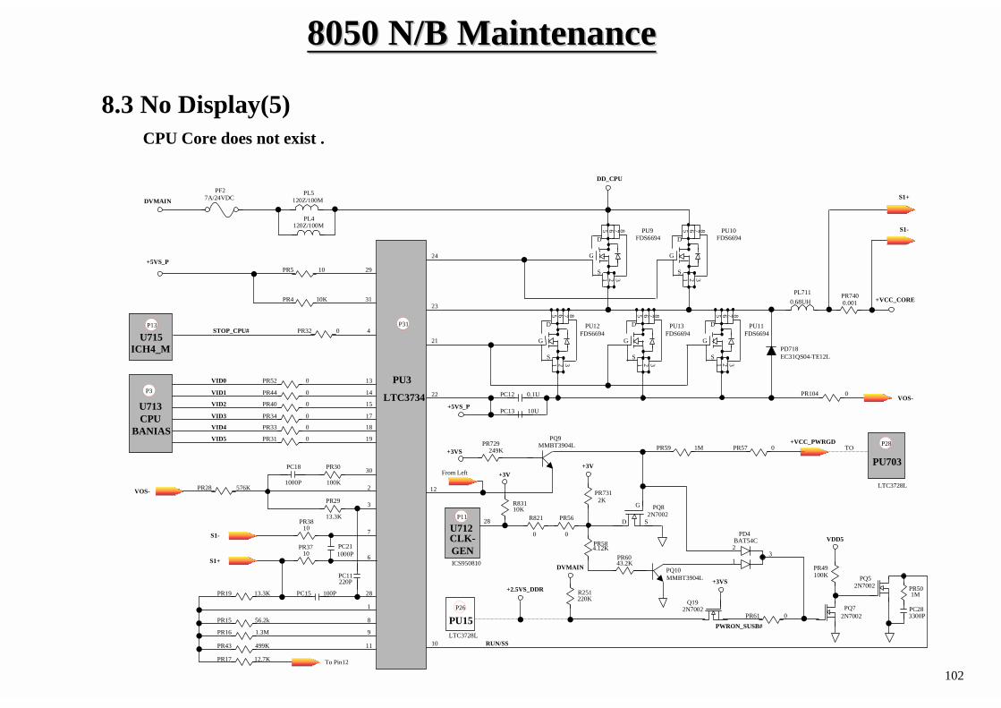
8050 8050 N/B MaintenanceN/B Maintenance
102
P31
PU3
LTC3734
G
D
S
2 316 7 85
D
S
2 316 7 85
G
+VCC_CORE
24
23
G
D
S
2 316 7 85
G
D
S2 31
6 7 85
G
D
S
2 316 7 85
21
22
DVMAIN
+5VS_P
STOP_CPU#P13
U715ICH4_M
PR32 0 4
PR104 0VOS-
PF27A/24VDC
PL5120Z/100M
PL4120Z/100M
PC12 0.1U
PC13 10U
PU9 PU10FDS6694 FDS6694
PR7400.001
PL7110.68UH
PD718EC31QS04-TE12L
2N7002
CPUBANIAS
P3VID0 PR52 0 13
14
15
17
18
19
PR44
PR40
VID1
VID2
VID3
VID4
VID5
0
0
PR34
PR33
PR31
0
0
0
U713
+5VS_PPR5 10 29
PR4 10K 31
S1+
S1-
PU12 PU13 PU11
DD_CPU
FDS6694 FDS6694 FDS6694
RUN/SS10
PR61 0
Q19
PWRON_SUSB#
VDD5
PQ5
2N7002PQ7
2N7002 PR501M
PC283300PPU15
P26
LTC3728L
DVMAIN
R251220K
+2.5VS_DDR
30
2
PR30
100K
PC18
1000PPR28 576K
PR29
13.3K
3
28100PPC15PR19 13.3K
1
8PR15 56.2k
7
6PR37
10
10PR38
PC211000P
S1+
S1-
PR43 11
PR17
VOS-
PC11220P
PR16 1.3M 9
499K
12.7K To Pin12
+3VS
PR7312K
PQ82N7002
+3V
PR729249K PR57
P28
PU703
LTC3728L
0PR59 1MPQ9
MMBT3904L
12
CLK-GEN
P11
ICS950810
+3VS
PD4BAT54C
PR49100K
PQ10MMBT3904L
U712
+VCC_PWRGD
G
28 D S
2
13
R83110K
+3V
PR584.12K
PR6043.2K
R821
0 0
PR56
TO
From Left
8.3 No Display(5)CPU Core does not exist .
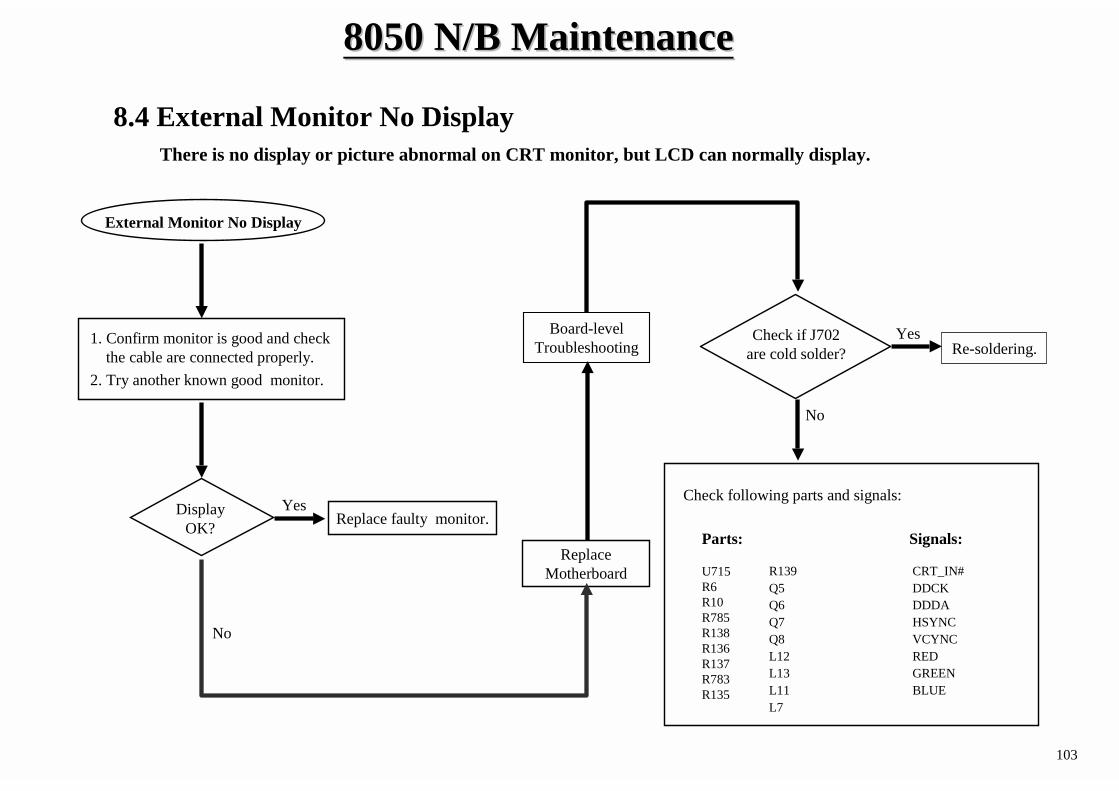
8050 8050 N/B MaintenanceN/B Maintenance
103
DisplayOK?
External Monitor No Display
1. Confirm monitor is good and checkthe cable are connected properly.
2. Try another known good monitor.
Replace faulty monitor.Yes
No
YesRe-soldering.
No
Parts:
U715R6R10R785R138R136R137R783R135
Signals:
Check if J702are cold solder?
CRT_IN#DDCKDDDAHSYNCVCYNCREDGREENBLUE
Board-levelTroubleshooting
ReplaceMotherboard R139
Q5Q6Q7Q8L12L13L11L7
Check following parts and signals:
8.4 External Monitor No DisplayThere is no display or picture abnormal on CRT monitor, but LCD can normally display.
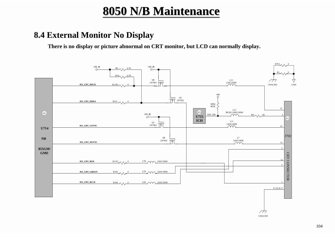
8050 8050 N/B MaintenanceN/B Maintenance
104
R10
R6+5V_H +5V_H
+5V_H 5
15
14
13
12
J702
CHAGND
R1 0
CHAGND GND
L12120Z/100M
Q62N7002
Q52N7002
L7120Z/100M
Q72N7002
Q82N7002
L13
U715CRT_IN#
BEAD_600Z/100MR9 1K
R804802K
+3V
855_CRT_DDCK
855_CRT_DDDA
855_CRT_VSYNC
855_CRT_HSYNC
855_CRT_RED
855_CRT_GREEN
855_CRT_BLUE
U714
855GM/GME
4.7K
4.7K
L11120Z/100M
ICH
3
2
1
6,7,8,16,17
P4
NB
P13
P12
CR
T CO
NN
ECTO
R
R1166
R331
R1167
R343
R344 L60
L59
L58
8.4 External Monitor No DisplayThere is no display or picture abnormal on CRT monitor, but LCD can normally display.
0
0
R703 0
0
0
0
220Z/100M
220Z/100M
220Z/100M
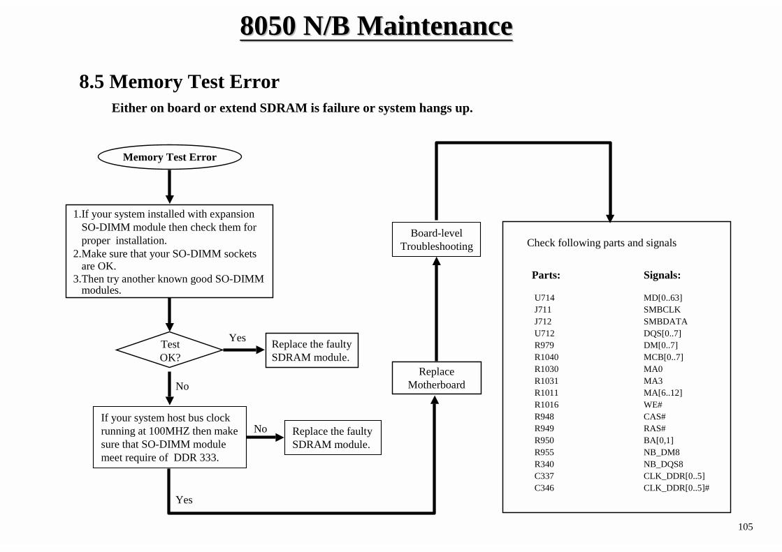
8050 8050 N/B MaintenanceN/B Maintenance
105
Memory Test Error
TestOK?
Replace the faulty SDRAM module.
Yes
No
Parts: Signals:
1.If your system installed with expansionSO-DIMM module then check them forproper installation.
2.Make sure that your SO-DIMM socketsare OK.
3.Then try another known good SO-DIMMmodules.
If your system host bus clockrunning at 100MHZ then makesure that SO-DIMM modulemeet require of DDR 333.
Replace the faulty SDRAM module.
No
Yes
MD[0..63]SMBCLKSMBDATADQS[0..7]DM[0..7]MCB[0..7]MA0MA3MA[6..12]WE#CAS#RAS#BA[0,1]NB_DM8NB_DQS8CLK_DDR[0..5]CLK_DDR[0..5]#
Board-levelTroubleshooting
ReplaceMotherboard
U714J711J712U712R979R1040R1030R1031R1011R1016R948R949R950R955R340C337C346
Check following parts and signals
8.5 Memory Test ErrorEither on board or extend SDRAM is failure or system hangs up.
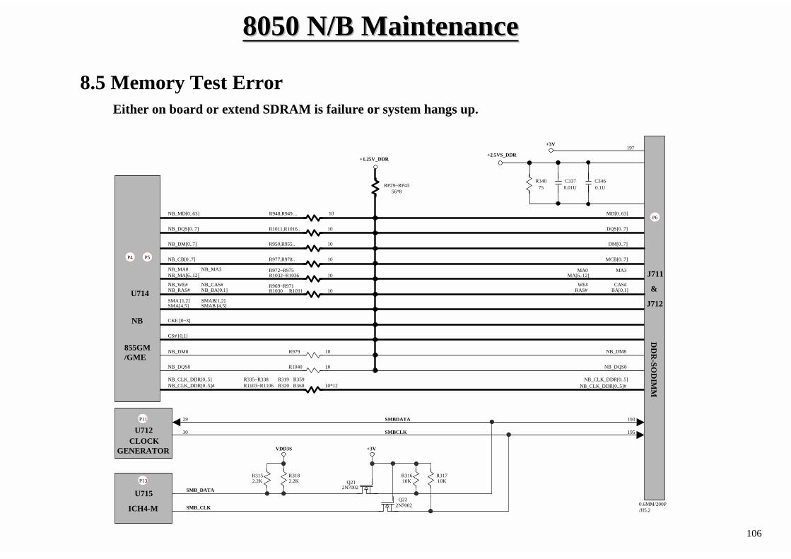
8050 8050 N/B MaintenanceN/B Maintenance
106
+1.25V_DDR
MD[0..63]
DQS[0..7]
DM[0..7]
MCB[0..7]
MA0 MA3MA[6..12]
WE# CAS#RAS# BA[0,1]
NB_DM8
NB_DQS8
NB_CLK_DDR[0..5]NB_CLK_DDR[0..5]#
J711
&
J712
+3V
+2.5VS_DDR
R340 C337 C34675 0.01U 0.1U
197
NB_MD[0..63]
NB_DQS[0..7]
NB_DM[0..7]
NB_CB[0..7]
NB_MA0 NB_MA3NB_MA[6..12]
NB_WE# NB_CAS#NB_RAS# NB_BA[0,1]
R948,R949…
R972~R975
R1031R969~R971
U714SMA [1,2]SMA[4,5]
SMAB[1,2]SMAB [4,5]
CKE [0~3]
CS# [0,1]
R1011,R1016..
R950,R955..
R977,R978..
R1032~R1036
10
10
10
10
10
R1030
NB_DM8
NB_DQS8
NB_CLK_DDR[0..5]NB_CLK_DDR[0..5]#
R979
R1040
R319R320
R335~R338 R359R360R1103~R1106
10
10
10
10*12
RP29~RP4356*8
U712CLOCK
GENERATOR
29 SMBDATA
30 SMBCLK
193
195
855GM/GME
0.6MM/200P/H5.2
P11
P6
DD
R-SO
DIM
M
P4 P5
NB
8.5 Memory Test Error
U715
ICH4-M
P13
+3VVDD3S
R3152.2K
R3182.2K Q21
R31610K
R31710K
Q22
2N7002
2N7002
SMB_DATA
SMB_CLK
Either on board or extend SDRAM is failure or system hangs up.
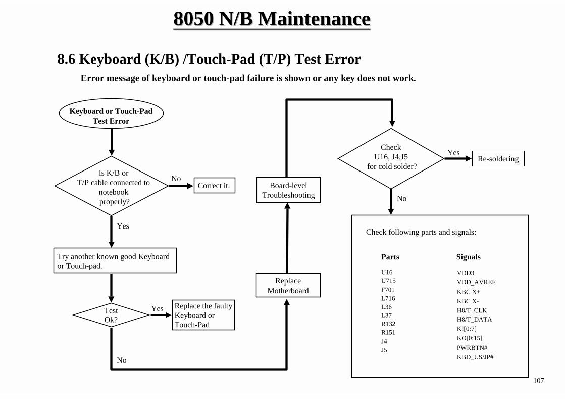
8050 8050 N/B MaintenanceN/B Maintenance
107
Keyboard or Touch-PadTest Error
Try another known good Keyboard or Touch-pad.
TestOk?
Replace the faulty Keyboard or Touch-Pad
Yes
No
CheckU16, J4,J5
for cold solder?
Yes
No
Re-soldering
Parts
U16U715F701L716L36L37R132R151J4J5
Signals
VDD3VDD_AVREFKBC X+KBC X-H8/T_CLKH8/T_DATAKI[0:7]KO[0:15]PWRBTN#KBD_US/JP#
Yes
NoCorrect it.
Is K/B orT/P cable connected to
notebookproperly?
Board-levelTroubleshooting
ReplaceMotherboard
Check following parts and signals:
8.6 Keyboard (K/B) /Touch-Pad (T/P) Test ErrorError message of keyboard or touch-pad failure is shown or any key does not work.
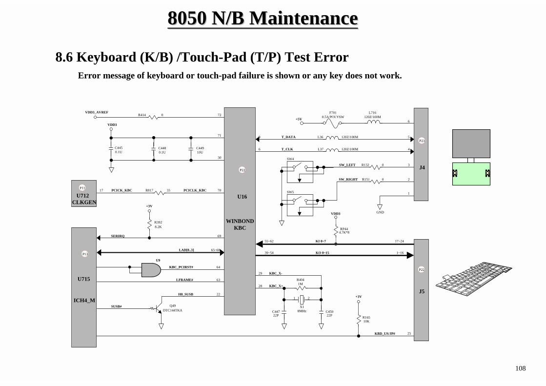
8050 8050 N/B MaintenanceN/B Maintenance
108
L716F701
+5V
J4
U16
KI 0~7
KO 0~15
J5
KBD_US/JP#
R165
U715
R132
L36
L37
GND
R151
VDD3
C445 C448 C449
WINBOND KBC
120Z/100M
120Z/100M
0.5A/POLYSW 120Z/100M
T_CLK
0
0
T_DATA9
6
SW_LEFT
SW_RIGHT
SW5
SW4
1~16
17~24
39~54
55~62
10K
25
C450
21
X18MHz
R4041M
C447
KBC_X+
KBC_X-29
28
22P 22P
ICH4_M
R3928.2K
69
LAD[0..3] 65~68
64
SERIRQ
KBC_PCIRST#
LFRAME#
SUSB#
H8_SUSB
Q49DTC144TKA
0.1U 0.1U 10U
71
30
VDD3_AVREFR414 0 72
+3V
63
22+3V
4
2
1
3
5
6
P23
U9
P22
P13
P22
VDD3
8.6 Keyboard (K/B) /Touch-Pad (T/P) Test Error
P11
U712CLKGEN
17 PCICK_KBC R817 33 PCICLK_KBC 70
RP444.7K*8
Error message of keyboard or touch-pad failure is shown or any key does not work.
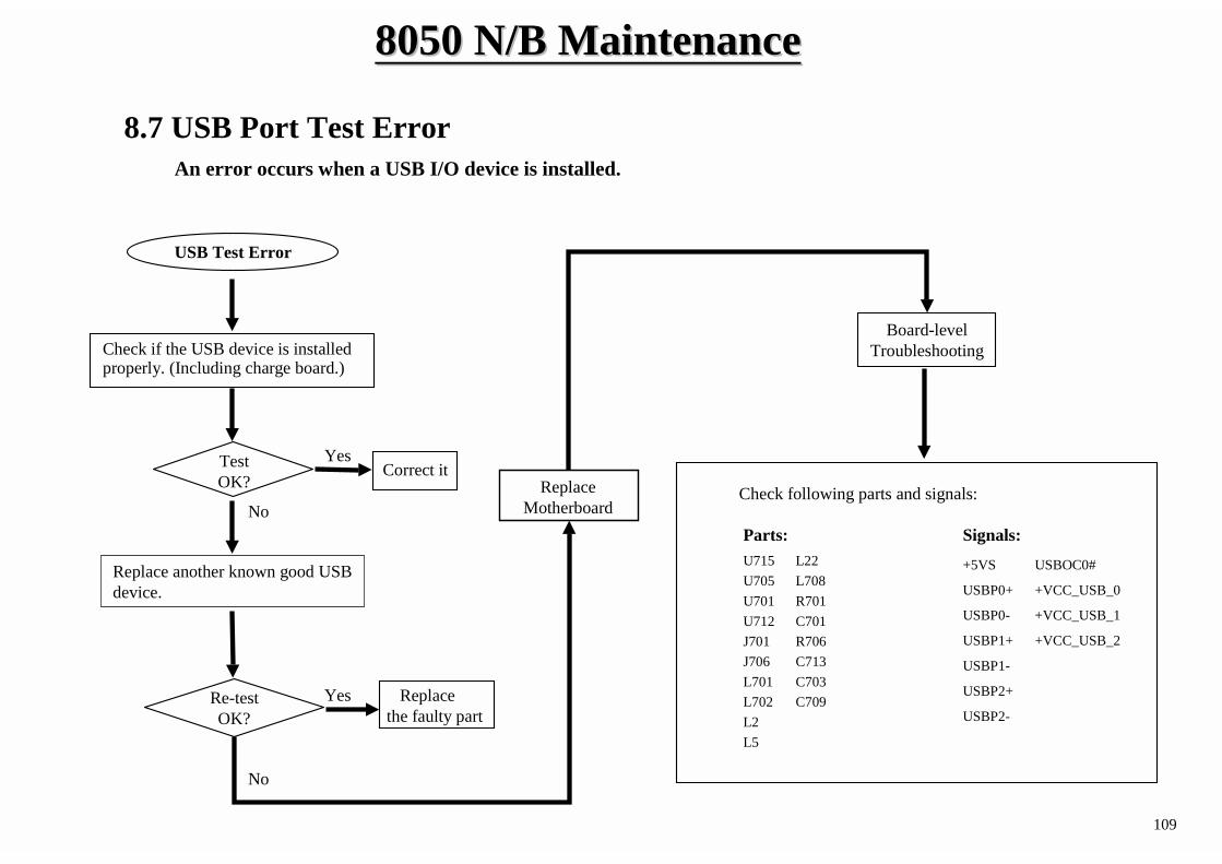
8050 8050 N/B MaintenanceN/B Maintenance
109
USB Test Error
Check if the USB device is installed properly. (Including charge board.)
Re-testOK?
No
Yes
No
YesCorrect it
Replace another known good USBdevice.
ReplaceMotherboard
Replacethe faulty part
TestOK?
Parts: Signals:U715U705U701U712J701J706L701L702L2L5
+5VS
USBP0+
USBP0-
USBP1+
USBP1-
USBP2+
USBP2-
Board-levelTroubleshooting
USBOC0#
+VCC_USB_0
+VCC_USB_1
+VCC_USB_2
Check following parts and signals:
L22L708R701C701R706C713C703C709
8.7 USB Port Test ErrorAn error occurs when a USB I/O device is installed.
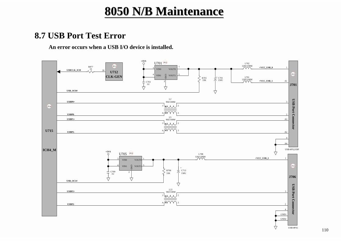
8050 8050 N/B MaintenanceN/B Maintenance
110
U715
ICH4_M
C701R701 L701
L702
C713
L708
USB_OC1#
USB_OC0#
+VCC_USB_0
J701+VCC_USB_1
1
A1
USBCLK_ICH
A4
4
1
+
+R70633K 150U
120Z/100M
+5VS
VOUT1
VIN0
GN
D
VOUT03
4
1
5
2
U705
VIN1
C7091U
150U33K
+5VS
VIN0
GN
D
VOUT03
4
1
5
2
U701
VIN1
C7031U
120Z/100M
120Z/100M
USB
Port Connector
U712CLK-GEN
39
+VCC_USB_2
USB/4PX2/DIP
J706
4
GND1
GND2
USB
Port Connector
USB/4PX1
34
1 2
L2
34
1 2
L5
34
1 2
L22
A2
A3
2
3
2
3
USBP0+
USBP0-
USBP1+
USBP1-
USBP2+
USBP2-
P15
P14
P15
P11
P15
P15
VOUT1
R877
90Z/100M
90Z/100M
90Z/100M
8.7 USB Port Test Error
33
An error occurs when a USB I/O device is installed.
8050 8050 N/B MaintenanceN/B Maintenance
111
Hard Driver Test Error
Yes
No
Parts: Signals:Re-bootOK? Replace the faulty parts.
1.Check the BIOS setup 2.Replace another good hard driver or
cable try again
Check the system driver for proper installation.
No
Re - TestOK?
End
U715J714Q37Q41L733R476R492R1081R1074
PCIRST#0PIORDYPDD[0..15]PDA[0..2]PDIOR#PDIOW#PDDACK#PDCS1#PDCS3#
Yes
Board-levelTroubleshooting
ReplaceMotherboard
PDDREQIRQ14+5V+5V_HDD
Check following parts and signals:
8.8 Hard Disk Drive Test ErrorEither an error message is shown, or the drive motor spins non-stop, while reading data from or writingdata to hard disk.
8050 8050 N/B MaintenanceN/B Maintenance
112
ICH4_M
U715
PD_D[0..15]
PDIOW#
PDIOR#
PIORDY
PDDACK#
IRQ14
PDA[0.. 2]
PDCS1#
PDCS3#
R1081 R1074
+3V
+5V
R492
R476
Q41
Q37
PCIRST#0 RSTDRV1#
J714
L733+5V 120Z/100M
4.7K 8.2K
10K
10K
DTC144TKA
DTC144TKA
27~42
22
20
18
16
14
9,10,12
8
7
HD
D C
ON
NE
CT
3
+5V_HDD
P15
P11
44
8.8 Hard Disk Drive Test ErrorEither an error message is shown, or the drive motor spins non-stop, while reading data from or writingdata to hard disk.
8050 8050 N/B MaintenanceN/B Maintenance
113
CD-ROM Driver Test Error
Yes
No
Parts: Signals:TestOK?
Correct it
Try another known good compact disk.
Check the CD-ROM driver for proper installation.
No
Re - TestOK?
Replacethe faulty parts.
U715J708Q37Q41R492R476R909R833R834L723
Yes
Board-levelTroubleshooting
ReplaceMotherboard
PCIRST#0RSTDRV2#SIORDYSDD[0..15]SDA[0..2]SDIOR#SDIOW#SDDACK#SDCS1#SDCS3#SDDREQIRQ15+5V+5V_CDROMCDROM_LEFTCDROM_RIGHT
CDROM_COMM
Check following parts and signals:
8.9 CD-ROM Test ErrorCD-ROM driver can’t run normally,maybe an error message is shown when reading data from CD-ROM.
8050 8050 N/B MaintenanceN/B Maintenance
114
R909
J708
CD
RO
M C
ON
NE
CT
ICH4_M
U715
SD_D[0..15]
SDIOW#
SDIOR#
SIORDY
SDDACK#
IRQ15
SDA[0.. 2]
SDCS1#
SDCS3#
R833 R834
+3V
+5V
R492
R476
Q41
Q37
PCIRST#0 RSTDRV2#
L723+5V 120Z/100M
4.7K 8.2K
10K
10K
DTC144TKA
DTC144TKA
6~21
25
24
27
28
29
31,33,34
35
36
38~42
0 5
+5V_CDROM
U726AUDIOCODEC
18
19
20
C507
C513
C515
1U
1U
0.22
R538
R547
R550
6.8K
0
6.8K
1
2
3
CDROM_LEFT
CDROM_COMM
CDROM_RIGHT
P15
P11
P20
R537R549 R5466.8K 6.8K 6.8K
8.9 CD-ROM Test ErrorCD-ROM driver can’t run normally,maybe an error message is shown when reading data from CD-ROM.
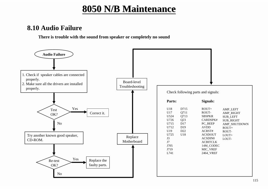
8050 8050 N/B MaintenanceN/B Maintenance
115
Test OK?
Audio Failure
1. Check if speaker cables are connectedproperly.
2. Make sure all the drivers are installed properly.
Try another known good speaker,CD-ROM.
Re-test OK?
Board-levelTroubleshooting
ReplaceMotherboard
YesCorrect it.
Yes
No
No
Parts:
U18U17U524U726U715U712U19U725J3J7J705J719L741
Signals:
ROUT+ROUT-SBSPKRCARDSPK#PC_BEEPAVDDACRST#ACSDOUTACSDIN0ACBITCLK14M_CODECMIC_VREF2464_VREF
Replace thefaulty parts.
Check following parts and signals:
D715Q711Q713Q23D17D19D22U18
AMP_LEFTAMP_RIGHT SUB_LEFTSUB_RIGHTAMP_SHUTDOWNROUT+ROUT-LOUT+LOUT-
8.10 Audio FailureThere is trouble with the sound from speaker or completely no sound
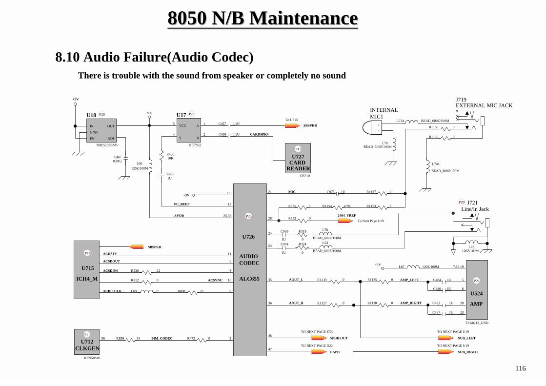
8050 8050 N/B MaintenanceN/B Maintenance
116
L70
L734U17
R1157
U715
+3V
ACSDOUT
ACRST#
ACSYNCR812
R530ACSDIN0
ACBITCLK L69 R498
U71214M_CODECR859 R472
AOUT_L
AOUT_R
R1130 AMP_LEFT
AMP_RIGHT
R1135
R1128
VA
7,18,19L67+5V
U524
R532
MIC
2464_VREF
J719
L744
0
+-
OUT
ADJ
GND
IN
EN
C467
U18
+5V
0.01UL66
R43810K
C4561U
BEAD_600Z/100M
BEAD_600Z/100M
BEAD_600Z/100M
SUB_RIGHT
SUB_LEFT
TPA0212_GND
0
120Z/100M
0
0
0
0R1127
MIC5205BM5
120Z/100M
5
4
U727
SBSPKRA
BY
VCC C457
C458 CARDSPK#
0.1U
0.1U
NC7S32
1
2
CB710
ICS950810
CLKGEN
ICH4_M
1,9
ALC655
11
5
822
10
60 22
0 35
36
256 33 0
12
25,38
PC_BEEP
AVDD
C492
C497
1U
1U
C484
C480
1U
5
6
20
23
1U
SBSPKR
To Next Page U19
TO NEXT PAGE U19
TO NEXT PAGE U19
EAPD
TO NEXT PAGE D22
P14
P11
P21
P20
P20P20
P17
AMP
EXTERNAL MIC JACK
U726
AUDIO CODEC
To U715
TO NEXT PAGE J720
SPDIFOUT
CARDREADER
24
24
C969
C9741U
1U
R519
R3240
0
L76
L53
J721Line/In Jack
P20
BEAD_600Z/100M
BEAD_600Z/100M
21
48
47
C975 1U
28
R1155
R1150
0
0
INTERNAL MIC1
R11540R535 R11534.7K 0
8.10 Audio Failure(Audio Codec)There is trouble with the sound from speaker or completely no sound
L751120Z/100M
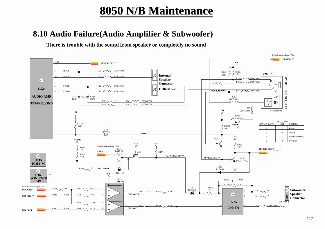
8050 8050 N/B MaintenanceN/B Maintenance
117
U715
ROUT+
ROUT-
LOUT+
LOUT-
L52
L50
L14
L16
21
16
4
9
C474 C489
R329 L80
+
J7
J3U524
C474
L78
+5V
R1158
D715
OPTIN#
DEVICE_DECT
SPDIFOUT
R1185
VA
+3V
Q711
Q713
Q23
R367
DECT_HP#OPT
L754
L55
Drive
LED
IC
AGND
J720
L757
DEVICE_DECT
+3V
D22
+5V
Q38 R477
AMP_SHUTDOWN
VDD3S
R906
R905
0
SUB_OUTR
SUB_OUTL
C496 R502
C483 R496U725
+5V
R27
5
8
6 L63
R26R1125
2464_VREF
SUB_RIGHT
SUB_LEFT
R479C482
R509C490
U19
31
2
75
6
VA
R511 R463
R510
100 22.1K
22.1K
0.15U 22.1K
0.15U 22.1K
EAPD
+
600Z/100M
600Z/100M
600Z/100M
600Z/100M
100U 100U
R528600Z/100M
2222
600Z/100M
600Z/100ML755
600Z/100M
600Z/100M
600Z/100M
L758600Z/100M
DTC144TKA
10K
DTA144WK
D19RLS4148
0
0
120Z/100MLM4871
0D17
RLS41488.2K
0.22U 8.2K
0.22U
BAT54C
LMV822
8.2K
10K
BAW56
HDR/MA-2
TPA0212_GND
ICH4_M
GP1FD310TP
HDR/MA-2
From Previous Page U726
From Previous Page U726
R3224.7K
R118310K
VA15,17
DEVICE_DECT#
10K
DEVICE_DECT#DECT_HP#/
OPT REMARK
0
1
0
1
0
1
0
1
HP in
OPT in
No this condition
No device
P21
P13
P21
P21
P21
HP/O
PT CO
NN
ECTOR
To U524
AUDIO AMP
From Previous Page U726
InternalSpeaker Connector
Subwoofer Speaker Connector
J705
KBC_MUTE
8.10 Audio Failure(Audio Amplifier & Subwoofer)There is trouble with the sound from speaker or completely no sound
1
4
R1122 2.1K
C471 1000P
D27
RLS4148
R445 0
80P2
U16WINBOND
KBC
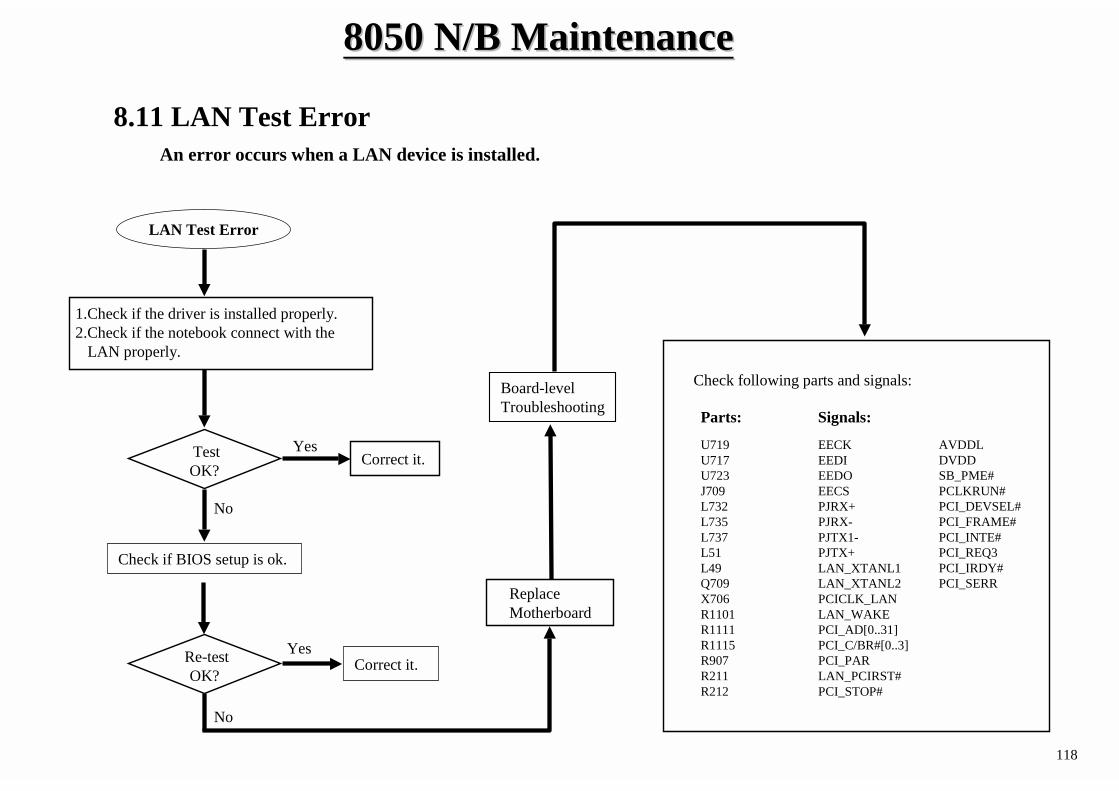
8050 8050 N/B MaintenanceN/B Maintenance
118
LAN Test Error
Yes
No
TestOK?
Correct it.
Correct it.
No
Check if BIOS setup is ok.
Re-testOK?
Board-levelTroubleshooting
ReplaceMotherboard
Parts: Signals:
1.Check if the driver is installed properly.2.Check if the notebook connect with the
LAN properly.
Yes
U719U717U723J709L732L735L737L51L49Q709X706R1101R1111R1115R907R211R212
Check following parts and signals:
EECKEEDIEEDOEECSPJRX+PJRX-PJTX1-PJTX+LAN_XTANL1LAN_XTANL2PCICLK_LANLAN_WAKEPCI_AD[0..31]PCI_C/BR#[0..3]PCI_PARLAN_PCIRST#PCI_STOP#
AVDDLDVDDSB_PME#PCLKRUN#PCI_DEVSEL#PCI_FRAME#PCI_INTE#PCI_REQ3PCI_IRDY#PCI_SERR
8.11 LAN Test ErrorAn error occurs when a LAN device is installed.
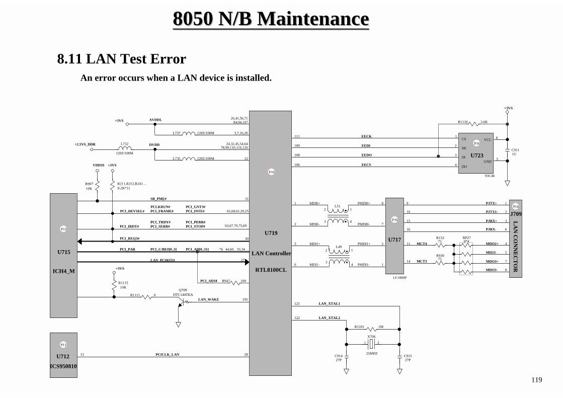
8050 8050 N/B MaintenanceN/B Maintenance
119
C911
+3VS
1
2
3
CS
SK
DI
DOGND
VCC
5
8
U723
U719
+3VS
R1111LAN_WAKE
Q709
U712 PCICLK_LAN
R907
VDD3S
U715
ICH4_M
PCI_AD[0..31]PCI_C/BE#[0..3]
PCI_DEVSEL# PCI_FRAME#PCI_GNT3#
PCI_REQ3#
PCI_INTE#
PCI_IRDY#PCI_TRDY#
PCI_PAR
PCI_PERR#PCI_SERR# PCI_STOP#
LAN_PCIRST#
+2.5VS_DDR L732 DVDD
+3VS
SB_PME#
PCLKRUN#
+3VS
LAN_XTAL1
LAN_XTAL2
R1101
X706
1 2
C914 C91525MHZ
RTL8100CL
PMDI0+
PMDI0-3 4
12L51
MDI0+
MDI0-
EECK
EEDI
EEDO
EECS
93C46
1U
10K
U717
LF-H80P
4
L735 120Z/100M
L737
MDI1+ PMDI1+
MDI1- PMDI1-3
4
12L49
J709PJTX1-
PJTX+
PJRX-
PJRX+
8
7
2
1
9
10
15
16
1
2
3
6
1
2
5
6
26,41,56,7184,94,107
3,7,16,20120Z/100M
AVDDL
120Z/100M12
24,32,45,54,6478,99,110,116,126
111
109
108
106
121
122
27P 27P
105DTC144TKA0
R111510K
2813
ICS950810
31
65,68,61,29,25
63,67,70,75,69
76 33,34…44,60..
R211,R212,R241…8.2K*11
LA
N C
ON
NE
CT
OR
1M
P16
P13
P16
P11
P16
P16
LAN ControllerMDO3+
MDO3-
MDO2+
MD23-
MCT4
MCT3
11
14
4
5
7
8
R152
R930
75
75
RP270*4
27
30
PCI_AD18 R947 100
8.11 LAN Test ErrorAn error occurs when a LAN device is installed.
R1110 3.6K
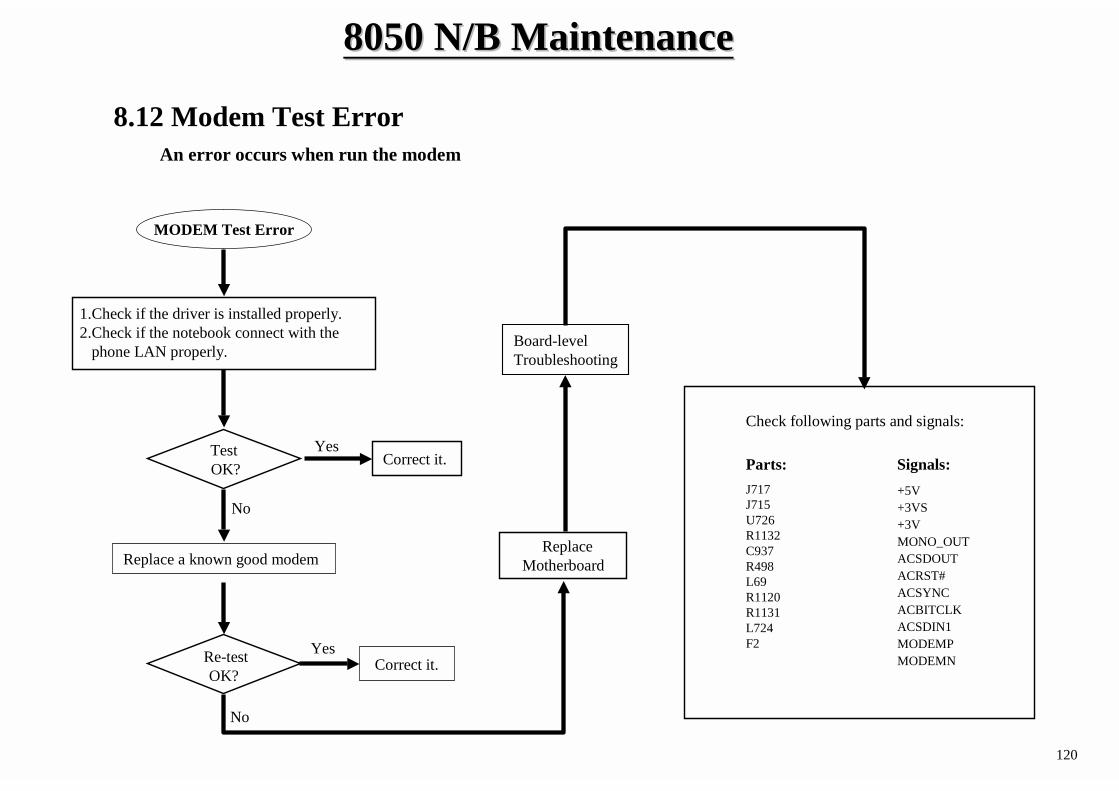
8050 8050 N/B MaintenanceN/B Maintenance
120
MODEM Test Error
No
TestOK?
No
Replace a known good modem
Re-testOK?
Board-levelTroubleshooting
1.Check if the driver is installed properly.2.Check if the notebook connect with the
phone LAN properly.
Correct it.
ReplaceMotherboard
Signals:
Yes
+5V+3VS+3VMONO_OUTACSDOUTACRST#ACSYNCACBITCLKACSDIN1MODEMPMODEMN
J717J715U726R1132C937R498L69R1120R1131L724F2
YesCorrect it. Parts:
Check following parts and signals:
8.12 Modem Test ErrorAn error occurs when run the modem
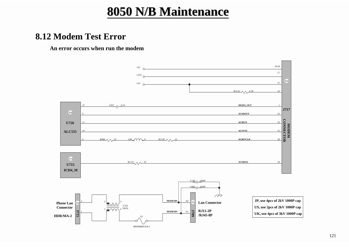
8050 8050 N/B MaintenanceN/B Maintenance
121
JP, use 4pcs of 2kV 1000P cap
US, use 2pcs of 2kV 1000P cap
UK, use 4pcs of 3kV 1000P cap
U726
MONO_OUT
J717ACSDOUT
ACRST#
C937
+3V
+3VS
ACSYNC
R498 L69 R1120
U715R1131
+5V
R1132
1 4
32
L724
J715
F2
J709
MODEMP
MODEMN
ACBITCLK
50UH
MO
DE
MC
ON
NE
CT
OR
0.1U
HDR/MA-2
2
1
MINISMDC014-2
37
5
11
10
6 22 0 22 30
22
25
23
1
16
21
17
10,18
22 24
4.7K
ACSDIN1
A2
A1
ALC555
ICH4_M
RJ11-2P/RJ45-8P
P20
P14
P20
P16Phone LanConnector
P20 Lan Connector
8.12 Modem Test ErrorAn error occurs when run the modem
C148
C806
1000P
1000P
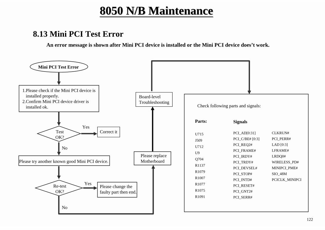
8050 8050 N/B MaintenanceN/B Maintenance
122
Please change the faulty part then end.
Correct it
Please try another known good Mini PCI device.
1.Please check if the Mini PCI device isinstalled properly.
2.Confirm Mini PCI device driver isinstalled ok.
Mini PCI Test Error
TestOK?
Re-testOK?
Yes
No
Yes
No
Parts:
U715
J509
U712
U9
Q704
R1137
R1079
R1007
R1077
R1075
R1091
Board-levelTroubleshooting
Please replaceMotherboard
Signals
PCI_AD[0:31]PCI_C/BE# [0:3]PCI_REQ2#PCI_FRAME#PCI_IRDY#PCI_TRDY#PCI_DEVSEL#PCI_STOP#PCI_INTD#PCI_RESET#PCI_GNT2#PCI_SERR#
CLKRUN#PCI_PERR#LAD [0:3]LFRAME#LRDQ0#WIRELESS_PD#MINIPCI_PME#SIO_48MPCICLK_MINIPCI
Check following parts and signals:
8.13 Mini PCI Test ErrorAn error message is shown after Mini PCI device is installed or the Mini PCI device does’t work.
8050 8050 N/B MaintenanceN/B Maintenance
123
R1007+3V
J713
U715
MINIPCI_LPCDRQ#R1075
R1079PCICLK_MINIPCI
R1083
R179R211..
+3V
R1091
PCI_PERR#PCLKRUN#
LAD[0..3]LFRAME#
+5V
SIO_48M R1137
U712
R895
R1068
PCI_INTD#PCI_GNT2#PCI_REQ2#
+3V
U9CPCIRST#R1077
9
108
R1080
+3V
R915
Q704
SB_PME#
PCI_AD[0..31]
121
PCI_STOP#PCI_DEVSE# WIRELESS_PD# 14,24
18,97
10K 13
PCI_FRAM#PCI_TRDY#
PCI_IRDY#PCI_SERR#
PCI_C/BE#[0..3]LRDQ0#
33
R816 33
39
11 25
260
0 MINIPCI_PME# 34
ICH4_M
MIN
IPCI C
ON
NE
CT
OR
ICS950810
P13P19
P11
P14
0
0
PCI_AD17
8.13 Mini PCI Test ErrorAn error message is shown after Mini PCI device is installed or the Mini PCI device does’t work.
48R1092 100
JL8
8050 8050 N/B MaintenanceN/B Maintenance
124
PC Card Slot Failure
1. Check if the PCMCIA CARD device is installed properly.
2. Confirm PCMCIA card driver is installed ok.
TestOK?
Re-testOK?
Yes
No
Yes
No
Change the faulty part then end.
Parts:
U727J716U728J6U9R186R180R211R212R1121R1129R826R1203
Try another known good PCMCIA card device.
Correct it
Board-levelTroubleshooting
ReplaceMotherboard
Signals
AD[0..31]C/BE# [0..3]DEVSEL#FRAME#IRDY#TRDY#STOP#PARPERR#SERR#P_REQ0#SERIRQ
PCIRST#P_GNT0#PIRQA#SUSB#RI#PCLK_CARDVCC5_EN#VCC3_EN#VPPD0VPPD1+VPPOUT+3V+5V
Check following parts and signals:
8.14 CardBus & Reader Test ErrorAn error occurs when a PC card device is installed.
8050 8050 N/B MaintenanceN/B Maintenance
125
CB710
U727
U715
ICH4_M
PCI_AD[0..31]
PCLKRUN#
8.2K*7
+3V
TPS2211A
U728
+3V3,4
+5V5,6
R1121
R1129
16
8
10K
10K
+CARD_VCC
J6
17,51
FM/34PX2/1.27MM
VCC5_EN#
VCC3_EN#
VPPD0
VPPD1
+VPPOUT 18,52
J716
PCICLK_CARD
ICS950810
12 R826 33
PCI_GNT0#
SUSB# R1200 4.7K
CARD_PCIRST#9
108
PCI_REQ0#
R1868.2k
PCI_FRAME#
R2318.2k*2
PCI_IRDY#PCI_TRDY#
PCI_DEVSEL# PCI_STOP#PCI_PERR#
PCI_SERR#
PCI_PAR PCI_C/BE#[0..3]
SERIRQ
VCCD0#
VCCD1#
VPPD0
VPPD1
R211,R212…
R180R1199R1201
10K*2+3V
MA/15PX2/ST
SDCD#
+SD_MSVDD20,27,29
MS_INS# MS_BS MS_SDIO2,12,14
SD_WP# SD_CMD1,4,6
R1198 10 SD_CLK7
8~11
CAD[0..31]
CCD2# CCD1# 36,67
CVS[1,2] 43,57
CCBE[0..3]#
R2_ A18 R2_ D2 4732,40R2_ D14
CBLOCK# 48~50CSTOP# CDEVSEL#
CTRDY# 13,15,53CPAR CGNT#
CSTSCHGCAUDIOCSERR# 59,62,63
CINT# CIRDY#CPERR# 14,16,20
CREQ#CRST#CFRAME# 54,58,60
CCLK 19R1213 33
7,12,21,61
2~6,8~11…
1
2
15
14
U712
U9
P17
P17
P17
P13
P11
P17
CLKGEN
SD C
ard
CardBusReader
R1202
8.14 CardBus & Reader Test ErrorAn error occurs when a PC card device is installed.
PCI_AD20 100
JL7
MS C
ard
5 R1203 10 MS_SCLK
SD[0..3]
8050 8050 N/B MaintenanceN/B Maintenance
126
TV Fail
1. Check if the TV device is installedproperly.
2. Confirm TV driver is installed ok.
Yes
No
TestOK?
Correct it.
Correct it.Yes
No
Check if BIOS setup is ok.
Re-testOK?
Board-levelTroubleshooting
ReplaceMotherboard
Parts: Signals
DOVCD[0..11]POUT/DET#TV_DDDATV_DDCKDVOVREFTV_PCIRST#855_TV_COMP855_TV_LUMA855_TV_CRMADVOCCLKDVOCCLK#DVOCVSYNC
U2J704U714U715U9Q702Q712L56L19L20C17C19C344R59R807R395
Check following parts and signals:
R162R113R114R157R111R112R115R128R147R1240R763R766X701
DVOCHSYNCXINXOUT
8.15 TV ENCODER Test FailureAn error occurs when using the computer as TV.
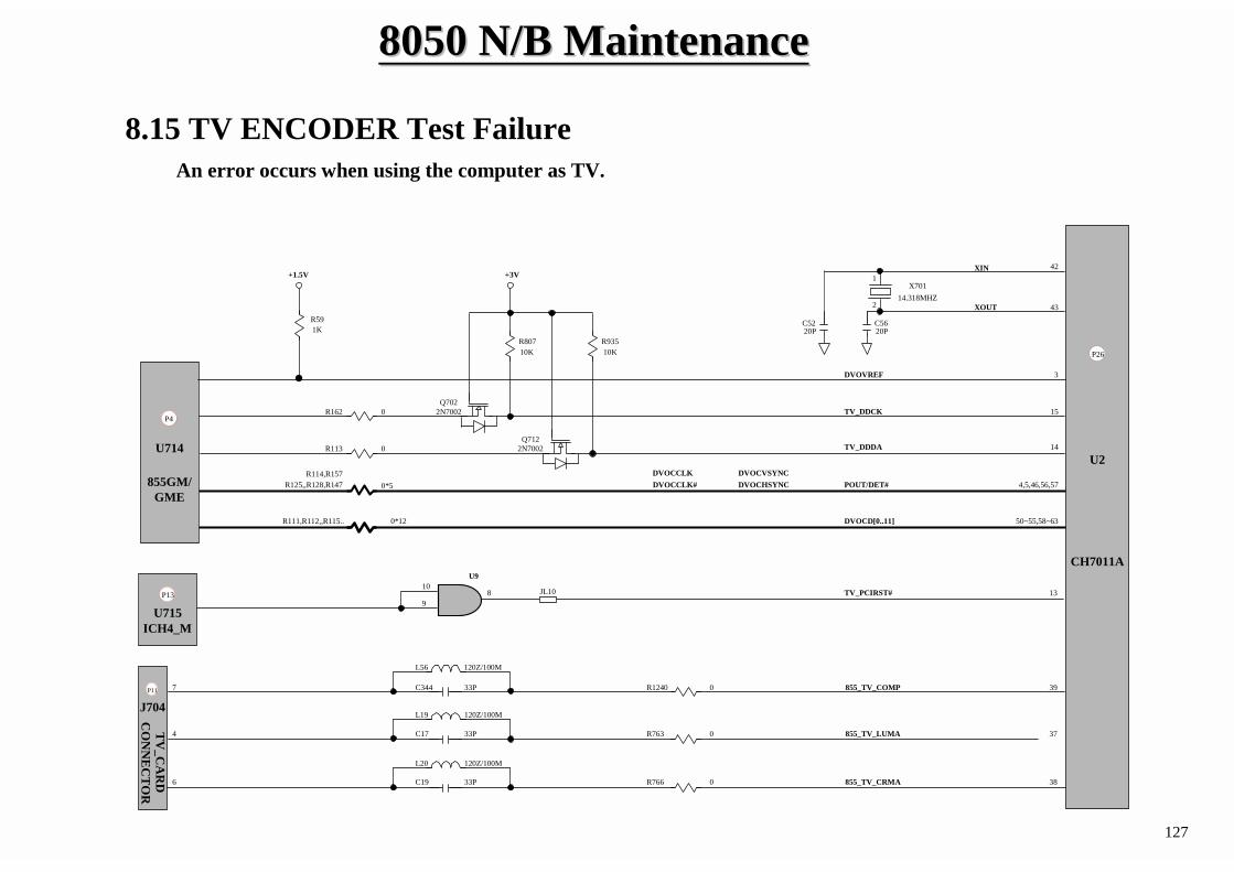
8050 8050 N/B MaintenanceN/B Maintenance
127
U714U2
CH7011A
XIN
XOUT
42
43
U715ICH4_M
TV_PCIRST#9
108 13
3
+1.5V
R591K
R114,R157855GM/
GME
DVOCCLKDVOCCLK# POUT/DET#0*5 DVOCHSYNCR125,,R128,R147
DVOCVSYNC4,5,46,56,57
DVOCD[0..11]R111,R112,,R115.. 50~55,58~63
J704
7
4
6
C344 33P
L56
L19
L20
120Z/100M
39
37
38
R1240
R763
R766 0
0
0
C17
C19
33P
33P
120Z/100M
120Z/100M
R162 15
14
Q702
R113Q712
TV_DDCK
TV_DDDA
0*12
2N7002
2N7002
+3VX701
14.318MHZ
1
2
DVOVREF
0
0
R807 R93510K 10K
855_TV_CRMA
855_TV_LUMA
855_TV_COMPP11
U9
P4
P13
TV
_CA
RD
CO
NN
EC
TO
R
P26
8.15 TV ENCODER Test FailureAn error occurs when using the computer as TV.
C52 C5620P20P
JL10
8050 8050 N/B MaintenanceN/B Maintenance
128
IEEE 1394 Fail
1. Check if the 1394 device is installedproperly.
2. Confirm 1394 driver is installed ok.
Yes
No
TestOK?
Correct it.
Correct it.Yes
No
Check if BIOS setup is ok.
Re-testOK?
Board-levelTroubleshooting
ReplaceMotherboard
Parts: Signals
PCI_AD[0..31]PCI_C/BE# [0..3]PC_DEVSEL#PCI_FRAME#PCI_IRDY#PCI_TRDY#PCI_STOP#PCI_PARPCI_PERR#PCI_REQ1#PCI_PME#+3V,+3VS+PHYVDD
1394_PCIRST#PCI_GNT1#EECS_1394EECK_1394EEDI_1394EEDO_1394TPBIASTPA+_6307TPA-_6307TPB+_6307TPB-_63071394_AVCCXIXO
U724U722J718U9U712U715L743L746L740L83R1117R828R1116R1142R1141X707
Check following parts and signals:
8.16 IEEE 1394 Test FailureAn error occurs when a IEEE 1394 device is installed..
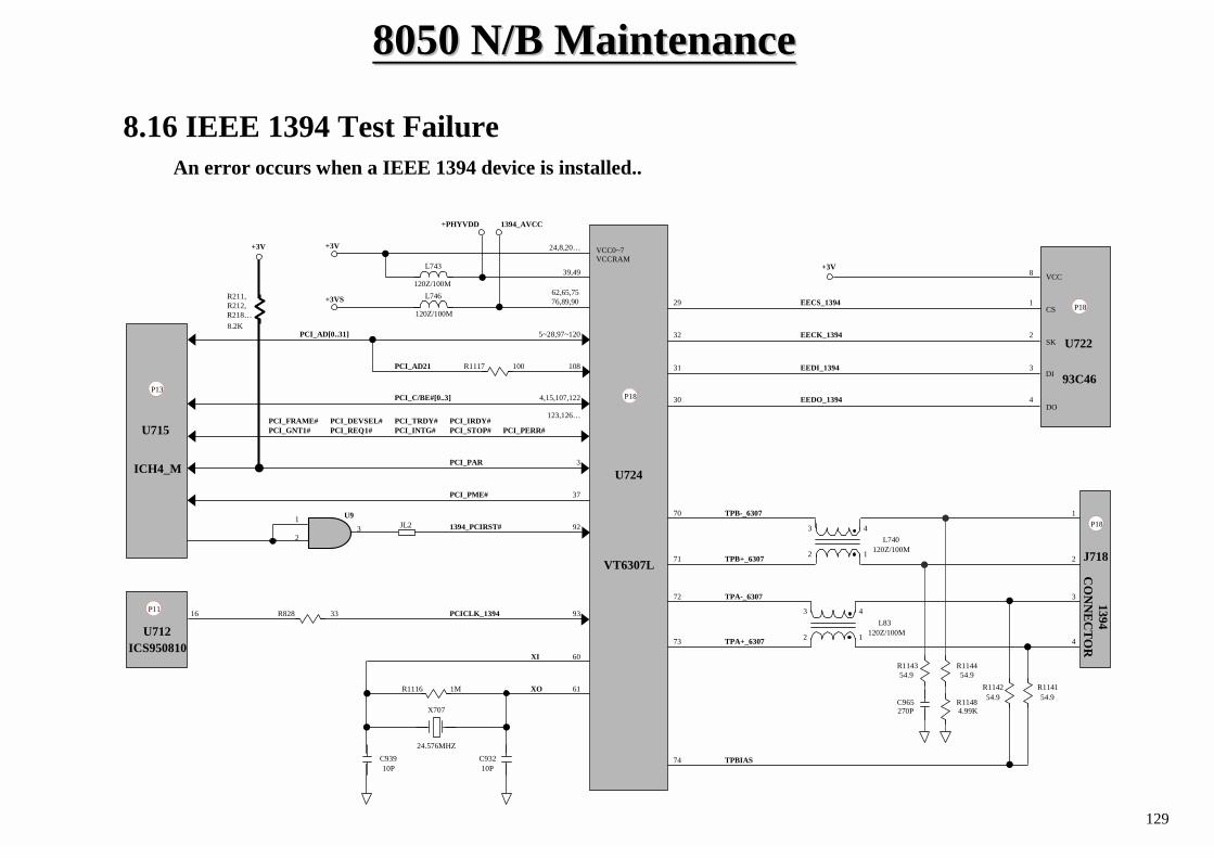
8050 8050 N/B MaintenanceN/B Maintenance
129
U724
VT6307L
U715
ICH4_M
PCI_AD[0..31] 5~28,97~120
PCI_C/BE#[0..3] 4,15,107,122
PCI_FRAME# PCI_DEVSEL# PCI_TRDY# PCI_IRDY#PCI_GNT1# PCI_REQ1# PCI_INTG# PCI_PERR#PCI_STOP#
PCICLK_1394
U712ICS950810
R828 33
1394_PCIRST#
93
2
13
U9
PCI_PAR 3
92
PCI_PME# 37
U722
93C46P18
EECS_1394
EECK_1394
EEDI_1394
EEDO_1394
1
2
3
4
CS
SK
DI
DO
8 VCC+3V
X707
24.576MHZC932C93910P10P
R1116 1M
XI
XO
60
61
2 1
43L740
120Z/100M
2 1
43L83
120Z/100M
TPB-_6307
TPB+_6307
TPA-_6307
TPA+_6307
J718
1
2
3
4
R1142 R114154.9 54.9
TPBIAS74
70
71
72
73
29
30
31
32
R1117 100PCI_AD21 108
VCC0~7+3V
VCCRAM
+PHYVDD
120Z/100M
L74339,49
+3VS
120Z/100M
L746
1394_AVCC
62,65,7576,89,90
+3V
R211,R212,R218…8.2K
24,8,20…
123,126…
16
1394C
ON
NE
CT
OR
P11
P13
P18
P18
8.16 IEEE 1394 Test FailureAn error occurs when a IEEE 1394 device is installed..
JL2
R1143 R1144
R1148C965270P
54.9
4.99K
54.9

8050 8050 N/B MaintenanceN/B Maintenance
130
Part Number Description Price(US)442672600031 AC ADPT ASSY;19V,3.16A,DELTA,706
361400003030 ADHESIVE;ABS+PC PACK,G485,CEMIDA
361400003005 ADHESIVE;HEAT,T RANSFER,HTA-48(W)
441681730001 BATT ASS'Y;11.1V,4.0Ah,LI,BL3244
441681730002 BATT ASSY;11.1V,4.0Ah,LI,CASE CL
441681730003 BATT ASSY;11.1V,4.0Ah,LI,CORE PA
338536010006 BATTERY;LI,3.6V/2.0AH,18650,PANA
340680900025 BEZEL ASSY;DVDRW,MKE,UJ815,8050
242670800113 BFM-WORLD MARK;WINXP,7521N
340680900006 BRACKET ASSY;SYSTEM,8050
340680900009 BRACKET ASSY;TP,8050
342672200010 BRACKET;CD-ROM,8500
322680900001 CABLE FFC;TP,8050
272075103408 CAP ;0.1U CR 50V 10% 0603 X7R S C10,C11,C12,C15,C3,C5,C6,C7,C8
272005104705 CAP ;1U CR 50V +80-20% 0805 Y5V C14A,C14B,C4A,C4B
272075101404 CAP; 0.001U CR 50V 10% 0603 X7R C13
272075471409 CAP; 0.0047U CR 50V 10% 0603 X7 C4
272075223702 CAP; 0.22U CR 50V +80-20% 0603 C1,C2,C20A,C24,C25
272105103702 CAP;.01U ,50V,+80-20%,0402,SMT C171,C176,C337,C339,C343,C386
272075103401 CAP;.01U ,CR,50V ,10%,0603,X7R,S C13,C8
272075103401 CAP;.01U ,CR,50V ,10%,0603,X7R,S C11,C3
272073223401 CAP;.022U,CR,25V ,10%,0603,X7R,S C9
272075473401 CAP;.047U,50V,10%,0603,X7R,SMT C313
272102473402 CAP;.047uF ,16V ,+-10%,0402,X7R, C841
272072824401 CAP;.082U ,16V ,10%,0603,X7R,SMT C16
Part Number Description Price(US)272071154401 CAP;.15U ,CR,10V,10%,0603,X7R,SM C482,C490
272105104701 CAP;.1U ,16V,+80-20%,0402,SMT C1000,C104,C12,C13,C133,C16,C
272102104401 CAP;.1U ,CR,10V,10%,0402,X5R,SM PC44
272072104402 CAP;.1U ,CR,16V,10%,0603,X7R,SM C17
272072104402 CAP;.1U ,CR,16V,10%,0603,X7R,SM C12,C6
272073104401 CAP;.1U ,CR,25V,10%,0603,X7R,PR C22,C7
272005104402 CAP;.1U ,50V,+/-10%,0805,X7R,SMT PC9
272005104404 CAP;.1U,CR,50V,10%,0805,SMT PC4,PC51,PC52,PC65,PC66,PC7,P
272102224701 CAP;.22U ,10V ,+80-20%,0402,Y5V, C14,C483,C496,C515
272071332401 CAP;.33U ,10V ,10%,0603,X7R,SMT C2
272102334701 CAP;.33U ,CR,10V ,+80-20%,0402,Y C964
272030102401 CAP;1000P,2KV,10%,1808,X7R,SMT C148,C327,C806
272105102501 CAP;1000P,50V ,+/-20%,0402,X7R,S C1006,C1007,C1008,C340,C357,C
272105102408 CAP;1000P,CR,50V,10%,0402,X7R,SM C960,C962,PC14,PC17,PC18,PC19
272075102403 CAP;1000P,CR,50V,10%,0603,X7R,SM C471
272105101402 CAP;100P ,50V ,+ -10%,0402,NPO,S C10,C330,C455,C498,C520,C521,C
272075101401 CAP;100P ,50V ,10%,0603,COG,SMT C20,C21
272105101401 CAP;100P ,50V ,5%,0402,COG,SMT C150,C18,C20,C503
272010101301 CAP;100P,2KV,5%,1206,NPO,SMT,onl C18
272010101302 CAP;100P,2KV,5%,1206,NPO,SMT,onl
272105100303 CAP;10P ,CR,50V ,5%,0402,NPO,SM C789,C790,C791,C795,C796,C797
272021106501 CAP;10U ,10V ,20%,1210,X7R,SMT C475
272011106701 CAP;10U ,10V,+80-20%,1206,Y5V,S C166,C174,C238,C271,C355,C772
272023106502 CAP;10U,25V,M,1210,T2.5MM,X5R,SM PC703,PC704,PC705,PC721,PC73
272001106702 CAP;10U,6.3V,+- 20%,0805,X5R,SMT C155,C156,C157,C158,C168,C173
9. Spare Part List(1)
8050 8050 N/B MaintenanceN/B Maintenance
131
Part Number Description Price(US)272431157507 CAP;150U ,TPC,6.3V,20%,H1.9,7343 C701,C713,C768,PC712,PC719,PC
272431157512 CAP;150U,6.3V,+/-20%,H2.8,PT,NCC
272105181403 CAP;180P,50V,10%,0402,SMT PC24,PC25,PC61,PC63,PC738
272001105403 CAP;1U ,10%,10V ,0805,X7R,SMT PC3,PC46
272012105401 CAP;1U ,CR,16V ,10%,1206,X7R,S C14A,C14B
272003105701 CAP;1U ,CR,25V ,+80%-20%,0805, PC701
272102105701 CAP;1U ,CR,6.3V ,80-20%,0402,Y C1002,C11,C160,C206,C210,C219
272071105403 CAP;1U ,10V ,10%,0603,X5R,SMT C10,C4
272002225701 CAP;2.2U ,CR,16V ,+80-20%,0805,Y C921,C961
272071225401 CAP;2.2U ,CR,6.3V ,10%,0603,X5R, C1001,C151,C161,C239,C24,C283
272105200401 CAP;20P ,50V,+-10%,0402,SMT C52,C56
272105222501 CAP;2200P,50V ,+/-20%,0402,X7R,S C470,C494,C509,C728,C869
272075222401 CAP;2200P,50V ,10%,0603,X7R,SMT C15A
272075222401 CAP;2200P,50V ,10%,0603,X7R,SMT C5
272105221403 CAP;220P ,CR,50V ,10%,0402,X7R,S C165,PC11,PC73,PC734,PC75
272431227504 CAP;220U ,4V ,20%,7343,POSCAP,SM PC729,PC749
272431227528 CAP;220U,2.5V,TPE-MC,20%,POSCAP, PC775,PC778,PC781,PC784,PC78
272105220402 CAP;22P ,50V ,+ -10%,0402,NPO,S C447,C450,C855,C861
272105271403 CAP;270P ,50V,+-10%,0402,X7R,SMT C15,C21,C782,C965
272105270303 CAP;27P ,50V ,5%,0402,COG,SMT C794,C804,C914,C915
272105332402 CAP;3300P,50V,10%,0402,SMT PC28,PC56
272431337506 CAP;330U,4V,20%,7343,SMT PC787,PC788
272103331401 CAP;33P ,25V ,+/-10%,0402,NPO,S C17,C19,C344
272023475401 CAP;4.7U ,25V ,10%,1210,X5R,SMT C1
272001475701 CAP;4.7U ,CR,10V ,+80-20%,0805,Y C311,C517,C871,C941,C947
Part Number Description Price(US)272070475701 CAP;4.7U,CR,6.3V,+80-20%,0603,Y5 C860,C908
272075471401 CAP;470P ,50V,10%,0603,X7R,SMT C15B
272105470402 CAP;47P ,50V ,+ -10%,0402,NPO,S C1,C143,C144,C154,C172,C2,C4,C
272030050302 CAP;5P,3KV,5%,1808,NPO,SMT,only C19
221673150002 CARD BOARD;FRAME,PALLET,8060
221673150003 CARD BOARD;TOP/BTM,PALLET ,8060
221600020252 CART ON;BATT ERY,CAIMAN,PWR
221673120003 CART ON;N-B,8060
431680900003 CASE KIT;8050,INTERGRAT E
335152000026 CFM-BAT;FUSE,THERMAL,NEC,SF91E
242678500005 CFM-INTEL;CENT RINO,NOTEBOOK,8081
273000500115 CHOKE COIL;400uH MIN,120mΩ MAX; L724
273000150313 CHOKE COIL;90OHM/100MHZ,20%,2012 L2,L22,L5
361200001018 CLEANNER;YC-336,LIQUID,STENCIL/P
331000000302 CON HOLDER;PCMCIA,UP,STANDOFF 0. J6
291000000023 CON;4-IN-1 MEMORY CARD,MS,SD,XD, J2
291000000706 CON;BATT ERY,7P,MA,2.5MM,R/A,C103 J703
331710015016 CON;D,FM,15P,3ROW,SUYIN,070912FR J702
291000622007 CON;DIMM,R/A,200P,.6,H9.2,REVERS J711
291000152603 CON;FPC/FFC,26P,1MM,R/A,KBD,SMT J5
331040050018 CON;HDR,BT B R/A,0.8MM,S-T ECH1507 J708
291000023008 CON;HDR,FM,15P*2,0.8MM.H5,R/A,SM J717
331030044019 CON;HDR,FM.22P*2,R/A,ST,ACE-1A2, J714
291000021105 CON;HDR,MA,11P*1,ACES,87213-1100 CN1
291000021105 CON;HDR,MA,11P*1,ACES,87213-1100 J1
9. Spare Part List(2)
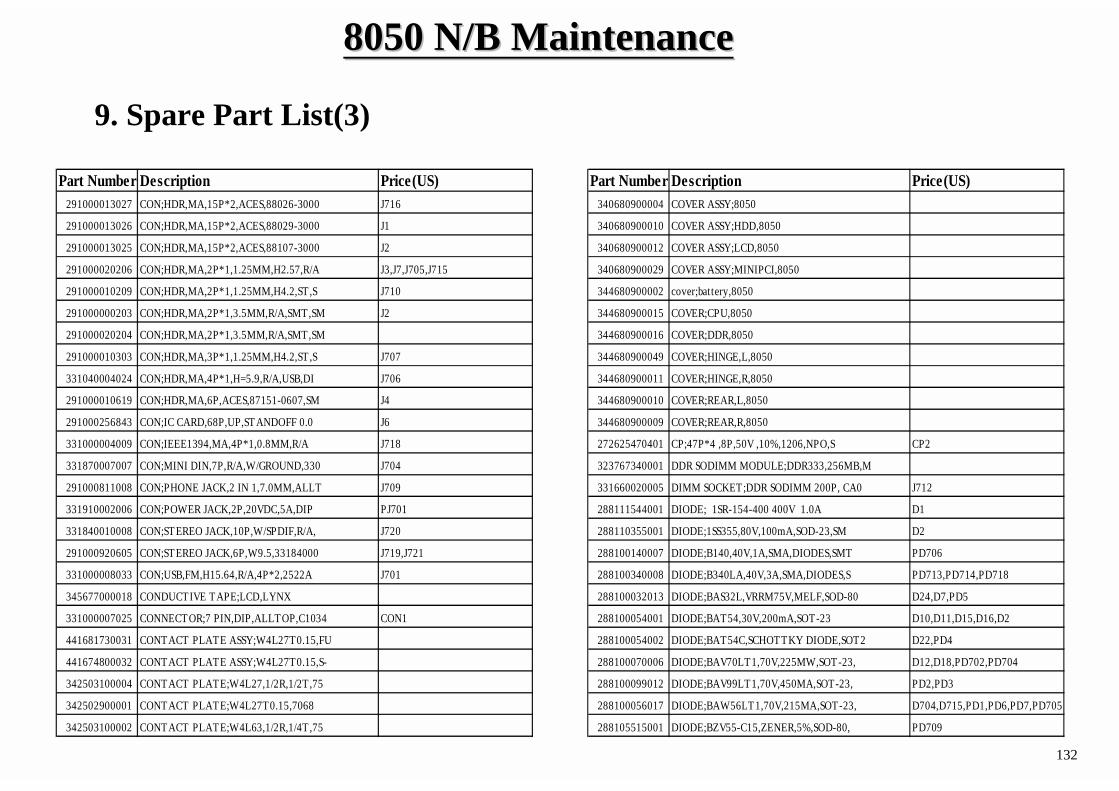
8050 8050 N/B MaintenanceN/B Maintenance
132
Part Number Description Price(US)291000013027 CON;HDR,MA,15P*2,ACES,88026-3000 J716
291000013026 CON;HDR,MA,15P*2,ACES,88029-3000 J1
291000013025 CON;HDR,MA,15P*2,ACES,88107-3000 J2
291000020206 CON;HDR,MA,2P*1,1.25MM,H2.57,R/A J3,J7,J705,J715
291000010209 CON;HDR,MA,2P*1,1.25MM,H4.2,ST,S J710
291000000203 CON;HDR,MA,2P*1,3.5MM,R/A,SMT,SM J2
291000020204 CON;HDR,MA,2P*1,3.5MM,R/A,SMT,SM
291000010303 CON;HDR,MA,3P*1,1.25MM,H4.2,ST,S J707
331040004024 CON;HDR,MA,4P*1,H=5.9,R/A,USB,DI J706
291000010619 CON;HDR,MA,6P,ACES,87151-0607,SM J4
291000256843 CON;IC CARD,68P,UP,ST ANDOFF 0.0 J6
331000004009 CON;IEEE1394,MA,4P*1,0.8MM,R/A J718
331870007007 CON;MINI DIN,7P,R/A,W/GROUND,330 J704
291000811008 CON;PHONE JACK,2 IN 1,7.0MM,ALLT J709
331910002006 CON;POWER JACK,2P,20VDC,5A,DIP PJ701
331840010008 CON;ST EREO JACK,10P,W/SPDIF,R/A, J720
291000920605 CON;ST EREO JACK,6P,W9.5,33184000 J719,J721
331000008033 CON;USB,FM,H15.64,R/A,4P*2,2522A J701
345677000018 CONDUCTIVE TAPE;LCD,LYNX
331000007025 CONNECT OR;7 PIN,DIP,ALLTOP,C1034 CON1
441681730031 CONTACT PLATE ASSY;W4L27T0.15,FU
441674800032 CONTACT PLATE ASSY;W4L27T0.15,S-
342503100004 CONTACT PLATE;W4L27,1/2R,1/2T,75
342502900001 CONTACT PLATE;W4L27T0.15,7068
342503100002 CONTACT PLATE;W4L63,1/2R,1/4T,75
Part Number Description Price(US)340680900004 COVER ASSY;8050
340680900010 COVER ASSY;HDD,8050
340680900012 COVER ASSY;LCD,8050
340680900029 COVER ASSY;MINIPCI,8050
344680900002 cover;battery,8050
344680900015 COVER;CPU,8050
344680900016 COVER;DDR,8050
344680900049 COVER;HINGE,L,8050
344680900011 COVER;HINGE,R,8050
344680900010 COVER;REAR,L,8050
344680900009 COVER;REAR,R,8050
272625470401 CP;47P*4 ,8P,50V ,10%,1206,NPO,S CP2
323767340001 DDR SODIMM MODULE;DDR333,256MB,M
331660020005 DIMM SOCKET;DDR SODIMM 200P, CA0 J712
288111544001 DIODE; 1SR-154-400 400V 1.0A D1
288110355001 DIODE;1SS355,80V,100mA,SOD-23,SM D2
288100140007 DIODE;B140,40V,1A,SMA,DIODES,SMT PD706
288100340008 DIODE;B340LA,40V,3A,SMA,DIODES,S PD713,PD714,PD718
288100032013 DIODE;BAS32L,VRRM75V,MELF,SOD-80 D24,D7,PD5
288100054001 DIODE;BAT54,30V,200mA,SOT-23 D10,D11,D15,D16,D2
288100054002 DIODE;BAT54C,SCHOTTKY DIODE,SOT2 D22,PD4
288100070006 DIODE;BAV70LT1,70V,225MW,SOT -23, D12,D18,PD702,PD704
288100099012 DIODE;BAV99LT1,70V,450MA,SOT-23, PD2,PD3
288100056017 DIODE;BAW56LT1,70V,215MA,SOT-23, D704,D715,PD1,PD6,PD7,PD705
288105515001 DIODE;BZV55-C15,ZENER,5%,SOD-80, PD709
9. Spare Part List(3)
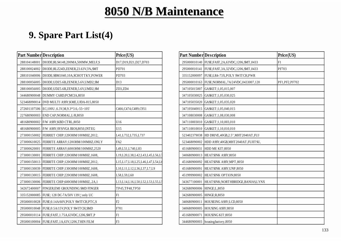
8050 8050 N/B MaintenanceN/B Maintenance
133
Part Number Description Price(US)288104148001 DIODE;RLS4148,200MA,500MW,MELF,S D17,D19,D21,D27,D703
288100024002 DIODE;RLZ24D,ZENER,23.63V,5%,SMT PD701
288101040006 DIODE;SBM1040,10A,SCHOTTKY,POWER PD703
288100056005 DIODE;UDZ5.6B,ZENER,5.6V,UMD2,SM D13
288100056005 DIODE;UDZ5.6B,ZENER,5.6V,UMD2,SM ZD3,ZD4
344680900048 DUMMY CARD;PCMCIA,8050
523468090014 DVD MULTI ASSY;KME,UJDA-815,8050
272601107506 EC;100U ,6.3V,M,9.3*3.6,-55~105' C466,C474,C489,C951
227680900003 END CAP;NORMAL,L/R,8050
481680900002 F/W ASSY;KBD CTRL,8050 U16
481680900005 F/W ASSY;SYS/VGA BIOS,8050,INT EG U15
273000150002 FERRIET CHIP;120OHM/100MHZ,2012, L41,L732,L735,L737
273000610025 FERRIT E ARRAY;120OHM/100MHZ,ONLY FA2
273000620001 FERRIT E ARRAY;600OHM/100MHZ,2520 L49,L51,L740,L83
273000130001 FERRIT E CHIP;120OHM/100MHZ,1608, L19,L20,L38,L42,L43,L45,L56,L7
273000150013 FERRIT E CHIP;120OHM/100MHZ,2012, L15,L17,L18,L25,L46,L47,L54,L6
273000130039 FERRIT E CHIP;130OHM/100MHZ,1608, L10,L11,L12,L36,L37,L7,L9
273000130015 FERRIT E CHIP;220OHM/100MHZ,1608, L58,L59,L60
273000130006 FERRIT E CHIP;600OHM/100MHZ,.2A,1 L13,L14,L16,L50,L52,L53,L55,L5
342672400007 FINGER;EMI GROUNDING SMD FINGER TP45,TP48,TP50
335152000085 FUSE; 128 DC-7A/50V 139only UC F1
295000010028 FUSE;0.14A/60V,POLY SWIT CH,PTC,S F2
295000010048 FUSE;0.5A/15V,POLY SWITCH,SMD F701
295000010114 FUSE;FAST,1.75A,63VDC,1206,SMT,P F1
295000100004 FUSE;FAST,1A,63V,1206,THIN FILM F3
Part Number Description Price(US)295000010140 FUSE;FAST,2A,63VDC,1206,SMT ,0433 F1
295000010141 FUSE;FAST,3A,32VDC,1206,SMT ,0433 PF703
335152000097 FUSE;LR4-73X,POLY SWITCH,PWR
295000010163 FUSE;NORMAL,7A/24VDC,0433007,120 PF1,PF2,PF702
347105015007 GASKET;1,05,015,007
347105030025 GASKET;1,05,030,025
347105035020 GASKET;1,05,035,020
347105040015 GASKET;1,05,040,015
347108030008 GASKET;1,08,030,008
347110003010 GASKET;1,10,003,010
347110010010 GASKET;1,10,010,010
523402379038 HD DRIVE,40GB,2.5",MHT2040AT,FUJ
523468090002 HDD ASSY;40GB,MHT2040AT,FUJITSU,
451680900031 HDD ME KIT ;8050
340680900013 HEATSINK ASSY;8050
451680900092 HEATSINK ASSY;MPT,8050
451680900091 HEATSINK ASSY;UNP,8050
451999900002 HEATSINK OPTION;8050
343677100001 HEATSINK;NORTHBRIDGE,BANIAS,LYNX
342680900006 HINGE;L,8050
342680900005 HINGE;R,8050
340680900011 HOUSEING ASSY;LCD,8050
340680900005 HOUSING ASSY;8050
451680900071 HOUSING KIT ;8050
344680900003 housing;battery,8050
9. Spare Part List(4)
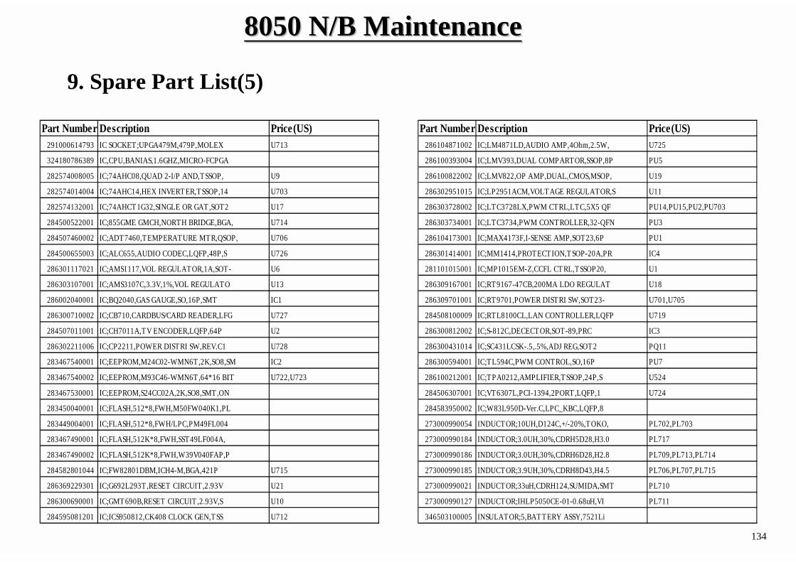
8050 8050 N/B MaintenanceN/B Maintenance
134
Part Number Description Price(US)291000614793 IC SOCKET ;UPGA479M,479P,MOLEX U713
324180786389 IC,CPU,BANIAS,1.6GHZ,MICRO-FCPGA
282574008005 IC;74AHC08,QUAD 2-I/P AND,TSSOP, U9
282574014004 IC;74AHC14,HEX INVERT ER,TSSOP,14 U703
282574132001 IC;74AHCT 1G32,SINGLE OR GAT ,SOT2 U17
284500522001 IC;855GME GMCH,NORTH BRIDGE,BGA, U714
284507460002 IC;ADT7460,TEMPERATURE MTR,QSOP, U706
284500655003 IC;ALC655,AUDIO CODEC,LQFP,48P,S U726
286301117021 IC;AMS1117,VOL REGULATOR,1A,SOT- U6
286303107001 IC;AMS3107C,3.3V,1%,VOL REGULATO U13
286002040001 IC;BQ2040,GAS GAUGE,SO,16P,SMT IC1
286300710002 IC;CB710,CARDBUS/CARD READER,LFG U727
284507011001 IC;CH7011A,TV ENCODER,LQFP,64P U2
286302211006 IC;CP2211,POWER DISTRI SW,REV.C1 U728
283467540001 IC;EEPROM,M24C02-WMN6T,2K,SO8,SM IC2
283467540002 IC;EEPROM,M93C46-WMN6T,64*16 BIT U722,U723
283467530001 IC;EEPROM,S24CC02A,2K,SO8,SMT,ON
283450040001 IC;FLASH,512*8,FWH,M50FW040K1,PL
283449004001 IC;FLASH,512*8,FWH/LPC,PM49FL004
283467490001 IC;FLASH,512K*8,FWH,SST49LF004A,
283467490002 IC;FLASH,512K*8,FWH,W39V040FAP,P
284582801044 IC;FW82801DBM,ICH4-M,BGA,421P U715
286369229301 IC;G692L293T,RESET CIRCUIT,2.93V U21
286300690001 IC;GMT 690B,RESET CIRCUIT ,2.93V,S U10
284595081201 IC;ICS950812,CK408 CLOCK GEN,TSS U712
Part Number Description Price(US)286104871002 IC;LM4871LD,AUDIO AMP,4Ohm,2.5W, U725
286100393004 IC;LMV393,DUAL COMPARTOR,SSOP,8P PU5
286100822002 IC;LMV822,OP AMP,DUAL,CMOS,MSOP, U19
286302951015 IC;LP2951ACM,VOLTAGE REGULATOR,S U11
286303728002 IC;LTC3728LX,PWM CTRL,LTC,5X5 QF PU14,PU15,PU2,PU703
286303734001 IC;LTC3734,PWM CONTROLLER,32-QFN PU3
286104173001 IC;MAX4173F,I-SENSE AMP,SOT23,6P PU1
286301414001 IC;MM1414,PROTECTION,T SOP-20A,PR IC4
281101015001 IC;MP1015EM-Z,CCFL CT RL,TSSOP20, U1
286309167001 IC;RT9167-47CB,200MA LDO REGULAT U18
286309701001 IC;RT9701,POWER DISTRI SW,SOT23- U701,U705
284508100009 IC;RTL8100CL,LAN CONTROLLER,LQFP U719
286300812002 IC;S-812C,DECECTOR,SOT-89,PRC IC3
286300431014 IC;SC431LCSK-.5,.5%,ADJ REG,SOT 2 PQ11
286300594001 IC;TL594C,PWM CONTROL,SO,16P PU7
286100212001 IC;TPA0212,AMPLIFIER,T SSOP,24P,S U524
284506307001 IC;VT6307L,PCI-1394,2PORT,LQFP,1 U724
284583950002 IC;W83L950D-Ver.C,LPC_KBC,LQFP,8
273000990054 INDUCTOR;10UH,D124C,+/-20%,TOKO, PL702,PL703
273000990184 INDUCTOR;3.0UH,30%,CDRH5D28,H3.0 PL717
273000990186 INDUCTOR;3.0UH,30%,CDRH6D28,H2.8 PL709,PL713,PL714
273000990185 INDUCTOR;3.9UH,30%,CDRH8D43,H4.5 PL706,PL707,PL715
273000990021 INDUCTOR;33uH,CDRH124,SUMIDA,SMT PL710
273000990127 INDUCTOR;IHLP5050CE-01-0.68uH,VI PL711
346503100005 INSULAT OR;5,BAT TERY ASSY,7521Li
9. Spare Part List(5)
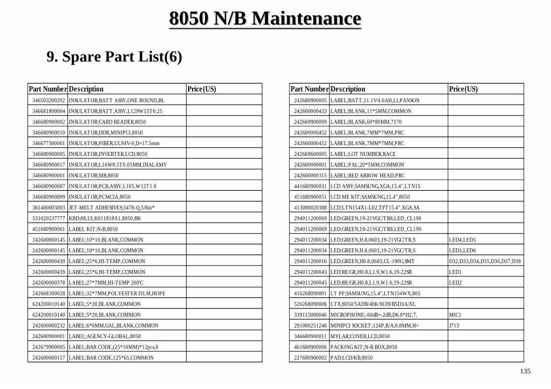
8050 8050 N/B MaintenanceN/B Maintenance
135
Part Number Description Price(US)346503200202 INSULAT OR;BAT T ASSY,ONE ROUND,BL
346681800004 INSULAT OR;BAT T,ASSY,L129W15T 0.25
346680900002 INSULAT OR;CARD READER,8050
346680900010 INSULAT OR;DDR,MINIPCI,8050
346677300001 INSULAT OR;FIBER,UL94V-0,D=17.5mm
346680900005 INSULAT OR;INVERTER,LCD,8050
346680900017 INSULAT OR;L16W8.5T0.05MM,DIALAMY
346680900001 INSULAT OR;MB,8050
346680900007 INSULAT OR;PCB,ASSY,L105,W12T1.0
346680900009 INSULAT OR;PCMCIA,8050
361400003003 JET-MELT ADHESIVES;3478-Q,5/8in*
531020237777 KBD;88,UI,K011818A1,8050,BK
451680900001 LABEL KIT;N-B,8050
242600000145 LABEL;10*10,BLANK,COMMON
242600000145 LABEL;10*10,BLANK,COMMON
242600000439 LABEL;25*6,HI-TEMP,COMMON
242600000439 LABEL;25*6,HI-TEMP,COMMON
242600000378 LABEL;27*7MM,HI-TEMP 260'C
242668300028 LABEL;32*7MM,POLYESTER FILM,HOPE
624200010140 LABEL;5*20,BLANK,COMMON
624200010140 LABEL;5*20,BLANK,COMMON
242600000232 LABEL;6*6MM,GAL,BLANK,COMMON
242680900001 LABEL;AGENCY-GLOBAL,8050
242679900005 LABEL;BAR CODE,(25*10MM)*12pcs,8
242600000157 LABEL;BAR CODE,125*65,COMMON
Part Number Description Price(US)242680900005 LABEL;BAT T,11.1V/4.0AH,LI,PANSON
242600000433 LABEL;BLANK,11*5MM,COMMON
242669900009 LABEL;BLANK,60*80MM,7170
242600000452 LABEL;BLANK,7MM*7MM,PRC
242600000452 LABEL;BLANK,7MM*7MM,PRC
242669600005 LABEL;LOT NUMBER,RACE
242600000001 LABEL;PAL,20*5MM,COMMON
242600000315 LABEL;RED ARROW HEAD,PRC
441680900031 LCD ASSY;SAMSUNG,XGA,15.4",LTN15
451680900051 LCD ME KIT;SAMSUNG,15.4",8050
413000020388 LCD;LTN154X1-L02,TFT15.4",XGA,SA
294011200069 LED;GREEN,19-21VGC/TR8,LED_CL190
294011200069 LED;GREEN,19-21VGC/TR8,LED_CL190
294011200034 LED;GREEN,H.8,0603,19-21VGC/TR,S LED4,LED5
294011200034 LED;GREEN,H.8,0603,19-21VGC/TR,S LED3,LED6
294011200016 LED;GREEN,H0.8,0603,CL-190G,SMT D32,D33,D34,D35,D36,D37,D38
294011200043 LED;RE/GR,H0.8,L1.9,W1.6,19-22SR LED1
294011200043 LED;RE/GR,H0.8,L1.9,W1.6,19-22SR LED2
416268090001 LT PF;SAMSUNG,15.4",LTN154WX,805
526268090006 LTX;8050/5ADB/40K/9UI9/B5D3A/XL
339115000046 MICROPHONE;-60dB+-2dB,D6.0*H2.7, MIC1
291000251246 MINIPCI SOCKET;124P,R/A,0.8MM,H= J713
346680900011 MYLAR;COVER,LCD,8050
461680900006 PACKING KIT;N-B BOX,8050
227680900002 PAD;LCD/KB,8050
9. Spare Part List(6)
8050 8050 N/B MaintenanceN/B Maintenance
136
Part Number Description Price(US)224670830002 PALLET ;1250*1080*130,7521N
221673150001 PART ITION;AK BOX,8060
221600050218 PART ITION;BATTERY,MARLIN,CAIMAN,
221673150004 PART ITION;PALLET,8060
221600050219 PART ITION;TOP/BTM,BATTERY,MARLIN
412681300001 PCB ASSY;D/A BD,DA-1A08-A,PWR
412678800001 PCB ASSY;FAX MODEM 56K,1456VQL4A
412673400008 PCB ASSY;MINI-PCI,T YPE IIIB,INTE
316680900003 PCB;PWA-8050 Card Reader_Transit R0B
316680900001 PCB;PWA-8050 M BD R01
316680900006 PCB;PWA-8050/BATT ,PR AND GA BD
316681300001 PCB;PWA-INVERTER BD (DA-1A08-A); R0E
222670820003 PE BAG;L560*W345,7521N
222503220001 PE BUBBLE BAG;BATTERY,GRAMPUS
273000150033 PHASEOUT;FERRITE CHIP,120OHM/100 L743,L746
411680900011 PWA;PWA-8050,MOT HER BD,INTERGRAT
411680900013 PWA;PWA-8050,MOT HER BD,SMT,INTER
411680900012 PWA;PWA-8050,MOT HER BD,T /U,INTER
411680900008 PWA;PWA-8050-CARD READER TRANSIT
411681300001 PWA;PWA-INVERTER BD,DA-1A08-A,PW
411681300004 PWA;PWA-INVERTER BD,SMT BOT,DA-1
411681300003 PWA;PWA-INVERTER BD,SMT TOP,DA-1
411681300002 PWA;PWA-INVERTER BD,SMT ,DA-1A08-
411681710001 PWA-PWA-BATT BD;LI,4.4Ah,2P3S,BL
411681710002 PWA-PWA-BATT BD;SMT ,BL3244G095/8
Part Number Description Price(US)332810000034 PWR CORD;250V/2.5A,2P,BLK,EU,175
271046017301 RES;.001,2W,5%,2512,CYNTEC,SMT PR740
271045087101 RES;.008 ,1W ,1% ,2512,SMT PR742
271045107101 RES;.01 ,1W ,1% ,2512,SMT PR701
271034127101 RES;.012,1/2W,1%,2010,WSL2010,VI PR707,PR711,PR719,PR732,PR73
271586026101 RES;.02 ,2W,1%,2512,SMT PR22
271002000301 RES;0 ,1/10W,5% ,0805,SMT L62,L65,L73,L88,R1,R123,R26,R2
271061000002 RES;0 ,1/16W,0402,SMT PR103,PR104,PR11,PR111,PR120
271071000002 RES;0 ,1/16W,5% ,0603,SMT L69,L719,L728,L744,L747,L751,L
271012000301 RES;0 ,1/8W,5% ,1206,SMT PR86
271044100101 RES;0.010,1.5W, 1%,2512,SMT;PWR R6
271045507103 RES;0.050,1W, 1%,2512,SMT, only R24A,R24B,R24C
271061010101 RES;1,1/16W,1%,0402,SMT PR18
271061135101 RES;1.3M,1/16W,1%,0402,SMT PR16,R1158
271061152501 RES;1.5K ,1/16W,5% ,0402,SMT R1084,R798
271071152302 RES;1.5K ,1/16W,5% ,0603,SMT R17
271071152302 RES;1.5K ,1/16W,5% ,0603,SMT R19
271061196212 RES;1.96K,1/16W,1%,0402,SMT PR710
271061100501 RES;10 ,1/16W,5% ,0402,SMT PR1,R1000,R1001,R1009,R1010,R
271061100102 RES;10,1/16W,1%,0402,SMT PR37,PR38,PR5
271061102312 RES;10.2K,1/16W,1% ,0402,SMT R496,R502
271061101103 RES;100 ,1/16W,1% ,0402,SMT R1092,R1117,R1202,R208,R257,R
271071101301 RES;100 ,1/16W,5% ,0603,SMT R11,R12,R14,R15,R16,R20,R21
271061104102 RES;100K ,1/16W,1% ,0402,SMT PR10,PR112,PR114,PR12,PR30,P
271071104101 RES;100K ,1/16W,1% ,0603,SMT R18,R22,R23,R9
9. Spare Part List(7)
8050 8050 N/B MaintenanceN/B Maintenance
137
Part Number Description Price(US)271061104501 RES;100K ,1/16W,5% ,0402,SMT PR69,PR703,PR720,PR83,PR89,R
271071104302 RES;100K ,1/16W,5% ,0603,SMT R7
271061107411 RES;107K,1/16W,1%,0402,SMT PR35
271061103102 RES;10K ,1/16W,1% ,0402,SMT PR102,PR119,PR4,PR47,PR724,P
271061103501 RES;10K ,1/16W,5% ,0402,SMT R1007,R1098,R11,R1103,R1115,R
271071103302 RES;10K ,1/16W,5% ,0603,SMT R2
271071103302 RES;10K ,1/16W,5% ,0603,SMT R5,R7,R8
271061106501 RES;10M ,1/16W,5% ,0402,SMT R296,R938
271061118211 RES;11.8K,1/16W,1%,0402,SMT PR116
271061127212 RES;12.7K,1/16W,1%,0402,SMT PR17
271061124312 RES;124K,1/16W,1%,0402,SMT PR79
271071127011 RES;127 ,1/16W,1% ,0603,SMT R14A
271071127011 RES;127 ,1/16W,1% ,0603,SMT R163
271061133311 RES;13.3K,1/16W,1%,0402,SMT PR19,PR29
271061137371 RES;13.7K,1/16W,.1%,0402,SMT PR74
271061133101 RES;13.7K,1/16W,1%,0402,SMT PR96
271071131101 RES;130 ,1/16W,1% ,0603,SMT R911
271071141102 RES;140 ,1/16W,1% ,0603,SMT R37
271061151102 RES;150 ,1/16W, 1%,0402,SMT R220,R446,R791,R850,R884,R912
271061153102 RES;15K ,1/16W,1% ,0402,SMT PR105,PR107,PR122,PR727,PR72
271061152302 RES;15K ,1/16W,5% ,0402,SMT R1008
271061180101 RES;18.2 ,1/16W,1% ,0402,SMT R838
271061184302 RES;180K ,1/16W, 5%,0402,SMT R1140,R288
271061183102 RES;18K,1/16W,1%,0402,SMT PR718,R462,R507
271061196213 RES;19.6K,1/16W,1%,0402,SMT PR36,PR97,PR99
Part Number Description Price(US)271061102105 RES;1K ,1/16W,1% ,0402,SMT PR121,PR53,R1006,R141,R328,R5
271061102303 RES;1K ,1/16W,5% ,0402,SMT R1136,R1147,R155,R181,R21,R25
271071102302 RES;1K ,1/16W,5% ,0603,SMT R11
271061105501 RES;1M ,1/16W,5% ,0402,SMT PR106,PR115,PR123,PR26,PR27,P
271071105301 RES;1M ,1/16W,5% ,0603,SMT R10,R3
271061222501 RES;2.2K ,1/16W,5% ,0402,SMT R315,R318
271061222101 RES;2.2K,1/16W,1%,0402,SMT PR6
271061232111 RES;2.32K,1/16W,1%,0402,SMT PR39
271061249211 RES;2.49K,1/16W,1% ,0402,SMT PR77
271061272102 RES;2.7K ,1/16W,1% ,0402,SMT R448,R449
271061205212 RES;20.5K,1/16W,1%,0402,SMT PR113
271071201301 RES;200 ,1/16W,5% ,0603,SMT R1A,R1B
271061201101 RES;200 ,1/16W, 1%,0402,SMT R280
271061204102 RES;200K ,1/16W,1% ,0402,SMT PR54,PR55
271061203701 RES;20K ,1/16W,.1%,0402,SMT PR75
271061203102 RES;20K ,1/16W,1% ,0402,SMT PR117,PR21,PR41,PR722,PR726,R
271061220501 RES;22 ,1/16W,5% ,0402,SMT R1120,R1131,R306,R329,R424,R4
271061220102 RES;22,1/16W,1% ,0402,SMT R253
271061221312 RES;22.1K,1/16W,1% ,0402,SMT R463,R479,R509,R510
271071221211 RES;22.1K,1/16W,1% ,0603,SMT R1122
271061221313 RES;220 ,1/16W, 5%,0402,SMT R552,R555,R556,R557
271061224501 RES;220K ,1/16W,5% ,0402,SMT R251
271071224301 RES;220K ,1/16W,5% ,0603,SMT R1
271061226311 RES;226K,1/16W,1%,0402,SMT PR71
271061223102 RES;22K,1/16W,1% ,0402,SMT R325,R520
9. Spare Part List(8)
8050 8050 N/B MaintenanceN/B Maintenance
138
Part Number Description Price(US)271061249212 RES;24.9K,1/16W,1%,0402,SMT PR98
271061249312 RES;249K,1/16W,1%,0402,SMT PR729,PR76
271061270102 RES;27.4 ,1/16W, 1%,0402,SMT R133,R213,R291
271071274811 RES;27.4 ,1/16W,1% ,0603,SMT R792,R839
271072287011 RES;287 ,1/10W,1% ,0603,SMT R914
271061202102 RES;2K ,1/16W,1% ,0402,SMT PR101,PR124,PR46,PR725,PR731
271071202301 RES;2K ,1/16W,5% ,0603,SMT R12
271061332312 RES;3.3K,1/16W,5% ,0402,SMT PR70
271071362101 RES;3.6K ,1/16W,1% ,0603,SMT R1110
271061301112 RES;301 ,1/16W,1% ,0402,SMT R793,R855
271071301311 RES;301K ,1/16W,1% ,0603,SMT R13,R3
271061330501 RES;33 ,1/16W,5% ,0402,SMT R1213,R816,R817,R818,R824,R82
271061331304 RES;330 ,1/16W,5% ,0402,SMT R1073,R1089,R301,R49,R54
271071331301 RES;330 ,1/16W,5% ,0603,SMT R16,R21,R22
271071331301 RES;330 ,1/16W,5% ,0603,SMT R18,R20,R23
271071331301 RES;330 ,1/16W,5% ,0603,SMT C14
271061333501 RES;33K ,1/16W,5% ,0402,SMT PR45,R701,R706
271071374812 RES;37.4 ,1/16W,1% ,0603,SMT R898
271061390501 RES;39, 1/16W, 5%,0402,SMT R225
271061391103 RES;390,1/16W,1% ,0402,SMT R876
271061412111 RES;4.12K,1/16W,1%,0402,SMT PR58
271071432111 RES;4.32K,1/16W,1% ,0603,SMT R10
271061442212 RES;4.42K,1/16W,1% ,0402,SMT R1127,R1130
271071478101 RES;4.7 ,1/16W,1% ,0603,SMT PR109,PR110,PR2,PR3,PR708,PR
271002472301 RES;4.7K ,1/10W,5% ,0805,SMT PR704,PR706
Part Number Description Price(US)271061472501 RES;4.7K ,1/16W,5% ,0402,SMT R10,R1081,R1132,R1154,R1200,R
271071472302 RES;4.7K ,1/16W,5% ,0603,SMT PR87,PR88
271061499212 RES;4.99K,1/16W,1% ,0402,SMT PR20,R1148
271061402011 RES;40.2 ,1/16W,1% ,0402,SMT R832
271071432211 RES;43.2K,1/16W,1% ,0603,SMT R1
271061432212 RES;43.2K,1/16W,1%,0402,SMT PR118,PR60,R1187,R1189,R1205,
271061471501 RES;470 ,1/16W,5% ,0402,SMT R1085,R553,R554,R558
271072474101 RES;470K ,1/10W,1% ,0603,SMT R4
271061474501 RES;470K ,1/16W,5% ,0402,SMT PR702,R373
271061473501 RES;47K ,1/16W,5% ,0402,SMT R442,R443,R702,R708,R929,R940
271071487811 RES;48.7 ,1/16W,1% ,0603,SMT R900
271071487011 RES;487 ,1/16W,1% ,0603,SMT,MUS R883
271061499012 RES;49.9 ,1/16W,1% ,0402,SMT R1082,R1086,R1087,R1090,R209,
271061499411 RES;499K ,1/16W,1% ,0402,SMT PR43,PR716
271071499311 RES;499K ,1/16W,1% ,0603,SMT R17
271061562102 RES;5.6K ,1/16W, 1%,0402,SMT R1099,R542
271061510303 RES;51, 1/16W, 5%,0402,SMT R224,R228,R238,R243,R289
271061549011 RES;54.9 ,1/16W,1% ,0402,SMT R1141,R1142,R1143,R1144,R142,
271061560501 RES;56 ,1/16W,5% ,0402,SMT R198,R264,R269,R273,R856,R936
271061562212 RES;56.2K,1/16W,1%,0402,SMT PR15
271071563101 RES;56K ,1/16W,1% ,0603,SMT R6
271061576411 RES;576K ,1/16W,1% ,0402,SMT PR28
271061590411 RES;590K,1/16W,1%,0402,SMT PR65
271061619211 RES;6.19K,1/16W,1% ,0402,SMT PR81
271061634211 RES;6.34K,1/16W,1% ,0402,SMT R1145
9. Spare Part List(9)
8050 8050 N/B MaintenanceN/B Maintenance
139
Part Number Description Price(US)271061649212 RES;6.49K,1/16W,1% ,0402,SMT PR721
271061682501 RES;6.8K ,1/16W,5% ,0402,SMT R537,R538,R546,R547
271061604011 RES;60.4 ,1/16W,1% ,0402,SMT R923,R924
271002604011 RES;604 ,1/10W,1% ,0805,SMT R945,R946
271061634214 RES;63.4K,1/16W,1%,0402,SMT PR42
271071681813 RES;68.1,1/16W,1%,0603,SMT R903
271061681501 RES;680 ,1/16W,5% ,0402,SMT R214
271071684101 RES;680K ,1/16W,1% ,0603,SMT R5
271061752102 RES;7.5K,1/16W,1%,0402,SMT PR84
271061750501 RES;75 ,1/16W,5% ,0402,SMT R152,R271,R277,R46,R930
271061753101 RES;75,1/16W,1%,0402,SMT R144,R145,R334,R340,R784
271071753301 RES;75K ,1/16W,5% ,0603,SMT R8
271071822102 RES;8.2K ,1/16W,1% ,0603,SMT R14B
271061822501 RES;8.2K ,1/16W,5% ,0402,SMT R1004,R1005,R1074,R1119,R1228
271061806311 RES;80.6K,1/16W,1% ,0402,SMT PR63,PR66
451680900151 ROM ME KIT;8050
271611000301 RP;0*4 ,8P ,1/16W,5% ,0612,SMT RP26,RP27
271611103301 RP;10K*4 ,8P ,1/16W,5% ,0612,SMT RP719
271621103302 RP;10K*8 ,10P,1/32W,5% ,1206,SMT RP46
271611220301 RP;22*4 ,8P ,1/16W,5% ,0612,SMT RP45
271621472302 RP;4.7K*8,10P,1/32W,5% ,1206,SMT RP44
271571560302 RP;56*8 ,16P,1/16W,5% ,1606,SMT RP29,RP30,RP31,RP32,RP33,RP3
271611750301 RP;75*4 ,8P ,1/16W,5% ,0612,SMT RP2
345677300001 RUBBER;SILICONE RUBBER,T =1.5mm,D
371102010252 SCREW;M2L2.5,K-HEAD(+),NIB/NLK
Part Number Description Price(US)371102010252 SCREW;M2L2.5,K-HEAD(+),NIB/NLK
340680900008 SHIELDING ASSY;COVER,8050
340680900026 SHIELDING ASSY;HDD,8050
333050000117 SHRINK TUBE;UL,600V,105'C,ID2.5*
342677000014 SMT NUT;A40M20-50,EMI STOP,LYNX MTG701,MTG702
342680900001 SMT NUT;A40M20-62,EMI STOP,8050 MTG703,MTG704
361400003021 SOLDER CREAM;NOCLEAN,P4020870980
361200003047 SOLDER PASTE;NO CLEAN,RMA,CK3000
365350000003 SOLDER WIRE;0.8MM,SN43/PB43/BI14
600100010009 SOLDER WIRE;63/37,0.8,CM,N/C,PRC
600100010009 SOLDER WIRE;63/37,0.8,CM,N/C,PRC
600100010009 SOLDER WIRE;63/37,0.8,CM,N/C,PRC
341680900001 SPC SCREW;#4-1/4,8050
370102010502 SPC-SCREW;M2 L5,NIB,K-HD,t0.8,NL
370102611601 SPC-SCREW;M2.6*L16,NIB,K-HD
370102610401 SPC-SCREW;M2.6L4,K-HD,t0.8,NIB/N
370102610401 SPC-SCREW;M2.6L4,K-HD,t0.8,NIB/N
370102610603 SPC-SCREW;M2.6L6,K-HD,NIB/NLK
370102610603 SPC-SCREW;M2.6L6,K-HD,NIB/NLK
370102010201 SPC-SCREW;M2L2,NIW,K-HD,t=0.8,NL
370102030301 SPC-SCREW;M2L3,K-HD,1,NIB/NLK
370102030301 SPC-SCREW;M2L3,K-HD,1,NIB/NLK
370102010303 SPC-SCREW;M2L3,NIW,K-HD(+),NYLOK
370102010409 SPC-SCREW;M2L4,K-HD(t0.3),NIB/NL
370102010409 SPC-SCREW;M2L4,K-HD(t0.3),NIB/NL
9. Spare Part List(10)
8050 8050 N/B MaintenanceN/B Maintenance
140
Part Number Description Price(US)370103010405 SPC-SCREW;M3L4,NIW,K-HD,T0.3
340680900002 SPEAKER ASSY;L,8050
340680900003 SPEAKER ASSY;R,8050
340680900001 SPEAKER ASSY;WOOFER,8050
226600030332 SPONGE;320*290*10,CAIMAN,PWR
346677000016 SPONGE;RTC,LYNX
341677000002 SPRING;SCREW,HEAT SINK,LYNX
523408610018 SUPER COMBO DRIVE;UJ-815B,PANASO
297140200003 SW;COVER SWITCH,0.1A,30V,4P,T -ME SW1
297004010001 SW;PUSH BUTTOM,5P,SPST,12VDC,50m SW2,SW4,SW5
225600000061 TAPE;ADHENSIVE,DOUBLE-FACE,W20,U
225600000054 TAPE;INSULATING,POLYEST ER FILM,1
310111103029 THERMIST OR;10K,1%,BN35-3H103F,18 RT1
442680900051 TOUCHPAD MODULE;SYNAPTICS,TM42PU
288227002006 TRANS;2N7002LT1,N-CHANNEL FET ,ES PQ1,PQ12,PQ14,PQ16,PQ17,PQ1
288204406001 TRANS;AO4406,N-MOS,.0165OHM,SO8 PU10,PU9
288204407001 TRANS;AO4407,P-MOS,.01OHM,SO8,SM PQ701,PQ704,PQ707
288204409001 TRANS;AO4409,P-MOSFET,SO-8P,MSL, Q3,Q5
288204410010 TRANS;AO4410,N-MOSFET,ID=18A,0.0 PU11,PU12,PU13
288204900001 TRANS;AO4900,DUAL N-MOSFET WITH PU4,PU6,PU702,PU705,PU707,PU
288204914001 TRANS;AO4914,DUAL N-MOSFET ,WITH PU701
288200144008 TRANS;DTA144EKA,PNP,SMT Q1
288204435003 TRANS;FDS4435,P-MOSFET ,35mOHM,SO Q9,U704,U707
288200301001 TRANS;FDV301N,N-CHANNEL,SOT23 Q42
288202222019 TRANS;MMBT2222ALT 1,NPN,TO236AB,O PQ15
Part Number Description Price(US)288203904022 TRANS;MMBT3904L,NPN,Tr35NS,TO236 PQ10,PQ9,Q20,Q708,Q718
288221371002 TRANS;MUN2137T1,PNP,SMT,ON PQ13,Q711
288202215001 TRANS;MUN2215T1,N-MOSFET ,SC59,SM Q719,Q720
288202237002 TRANS;MUN2237T1,NPN,SOT -23,SMT ,O PQ24,Q47
288202240001 TRANS;MUN2240T1,NPN,SOT -23,ON Q12,Q23,Q26,Q27,Q29,Q31,Q32,Q
288202301001 TRANS;SI2301DS,P-MOSFET,SOT -23 Q13,Q14,Q24,Q43,Q48,Q51
288204800001 TRANS;SI4800DY,N-MOS,.0185OHM,SO U7
273001050069 TRANSFORMER;10/100 BASE,NS0013,S
332110020165 WIRE ;#20AWG,UL1007,L=160mm,RED, CN1
332110020173 WIRE ;#20AWG,UL1007,L=256mm,BLAC CN4
332110026151 WIRE ;#26AWG,UL1007,L=142mm,YELL CN3
332110026150 WIRE ;#26AWG,UL1007,L=208mm,BLUE CN2
422677000008 WIRE ASSY;BATT T O MB,FOR LYNX,MO J710
340680900028 WIRE ASSY;INVERTER,8050
422674300071 WIRE ASSY;MDC,E-NOTE
422680900003 WIRE CABLE;SAM LT N154X1,8050
340680900027 WLEN ASSY;CABLE,8050
273001050160 XFMR;CI8.5,25T/2150T,300mH,ONLY T1
273001050039 XSFORMER;10/100 BASE,LF-H80P,SMT U717
274011431414 XT AL;14.318MHZ,32PF,50PPM,8*4.5, X701,X703
274012457406 XT AL;24.576MHZ,16PF,50PPM,8*4.5, X707
274012500415 XT AL;25MHZ,20PF,30PPM,8.0*4.5,SM X706
274013276103 XT AL;32.768KHZ,20PPM,12.5PF,CM20 X704
274010800405 XT AL;8Mhz,30PPM,16PF,8*4.5,2P,SM X1
P/N: 526268090006
9. Spare Part List(11)
PDF created with FinePrint pdfFactory trial version http://www.fineprint.com
5
5
4
4
3
3
2
2
1
1
D D
C C
B B
A A
PAGE 8 VGA-M10(2/4)
PAGE26 +2.5VS_DDR_P/+1.25V_DDR_P
PRODUCT CODE- 6809
PAGE24 PULL HIGH
PAGE 9 VGA-M10 (3/4)
PAGE18 IEEE1394
PAGE 7 VGA-M10(1/4)
PAGE17 R5C811/841
PROJECT CODE- G095
PAGE 2 CPU- BANIAS(1/2)
PCB P/N 316680900001
PAGE22 KBC(W83L950D)
PAGE11 CLOCK SYNTHERIZER/TV ENCODER
PAGE23 TOUCHP_PAD/FWH/LED
PAGE12 CRT/LCD
PAGE19 MINI-PCIPAGE20 AUDIO CODEC(ALC655)
PAGE10 VGA-M10(4/4)
PAGE 6 DDR-DIMM
PAGE15 CDROM/HDD/USB CONNECTOR
PAGE21 AUDIO AMPLIFIER/SUBWOOFER
PAGE25 PERPHERIAL
PAGE14 SOUTHBRIDGE-ICH4-M(2/2)
8050 R01
PAGE 1 TITLE
PAGE 5 NB-MONTARA-GME(2/2)
PAGE13 SOUTHBRIDGE-ICH4-M(1/2)
PAGE 3 CPU-BANIAS(2/2)
PAGE16 LAN RTL8100CL
ASSY P/N 411680900011
PAGE 4 NB-MONTARA-GME(1/2)
LAN PCI_INTE#
TAPEOUT DAY
CARDBUS /CARDREADER
AD18
2003/8/26
HISTORY
PCI_REQ3# /PCI_GNT3#
INTERRUPT
REVISION
R00PCI DEVICE
PCI_INTB# /PCI_INTC#
REQ/GNT
AD20
IDSEL
光學定位點
ISSUESCHECKDESIGNDRAWN
AD21PCI_INTG#IEEE1394
AD17MINIPCI
PCI_REQ0# /PCI_GNT0#
PCI_REQ1# /PCI_GNT1#
PCI_INTD# PCI_REQ2# /PCI_GNT2#
MDC CARDREADER
CPU
PAGE27 +3VS_P/+5VS_P
PAGE30 +1.2V/1.0V_M10
PAGE28 +1.5V_P/+1.05V_P
PAGE33 CHARGER/DISCHARGER
PAGE31 CPUCORE
PAGE29 +1.8V_P/1.35V_P
PAGE32 ADAPTER/VMAIN
R0A 2003/10/09
CHANGE MDC AND MINIPCI CONNECTORS PLACEMENT FROMSOLDER SIDE TO COMPONENT SIDE
4. CHANGE CARDBUS CONNENTOR PLACEMENT FORMCOMPONENT SIDE TO SOLDER SIDE
CHANGE LVDS ROUTING FAR AWAY POWER SWITCHINGSIGNALS
6.
3.
2. USE IEEE1394 CONTROLLER VT6307 INSTEAD OFR5C592
ADD SPDIF FUNCTION
5.
CHANGE CARDBUS/CARD READER CONTROLLER FROMR5C592 TO CB710
EMI2003/11/07R0B
1.
1. CHANGE TV CONNECTOR
EC
R01 2003/12/16
2. CHANGE BATTERY CONNECTOR
1. EXCHANGE TV CONNECTOR PIN 6 AND PIN 72. ADD SPREAD SPECTRUM CIRCUIT BUT RESERVE3. ADD POWER CONSUMPTION SAVING CIRCUIT BUT RESERVE
ESD
8050N
PCB 316680900001/ASSY 411680900011 R01
8050 MOTHER B/D
C
1 34Monday, December 29, 2003
Title
Size DocumentNumber
Rev
Date: Sheet of
GND GND_45 GND
GND_45GND GND
1394_GND
GND GND GND
GND GND
GND GND
GND GND
GND
CHAGND
CAGND
AGND
GND
GND
GND
GND
GND
GND GND GNDGND
GND GNDGNDGND
GND
GND
+5V+3V
+5V+3V
+1.35V
GND
GND
GND
GND
+2.5V_M10
GND_USB 1394_GND
GND GND
TP46
TOUCHPAD_METAL10
1
MTG2ID3.0/OD11MTG118-RD433-N-30X16
4567
9 10123
8
11
1213141516
TP4
TOUCHPAD_METAL5
1
FD703FIDUCIAL-MARK
1
FD2FIDUCIAL-MARK
1
TP44
TOUCHPAD_METAL10
1
MTG13ID3.0/OD11MTG118-RD433-N-30X16
4567
9 10123
8
11
1213141516
MTG1ID3.0/OD11MTG118NRD433_3016B
4567
9 10123
8
11
1213141516
TP52
TOUCHPAD_METAL10
1
MTG32ID5.3/OD7.5
1
TP48
TOUCHPAD_METAL10
1
TP45
TOUCHPAD_METAL10
1
MTG3ID3.0/OD9.0MTG118-RD354-N-30X12
456
7 9
10
1238
1112
FD701FIDUCIAL-MARK
1
MTG28ID5.3/OD7.5
1
C1007
1000P040250V
+/-20%1 2
FD1FIDUCIAL-MARK
1
MTG14ID3.0/OD11MTG118NRD433_3016B
4567
9 10123
8
11
1213141516
MTG701MTG/ID1.2/OD4.6
342677000014
1
MTG12ID5.3/OD7.5
1
MTG22ID2.8/OD11
1
MTG24ID5.3/OD7.5
1
MTG9ID3.0/OD11MTG118-RD433-N-30X16
4567
9 10123
8
11
1213141516
MTG7ID3.0/OD11MTG118NRD433_3016A
4567
9 10123
8
11
1213141516
MTG703MTG/ID1.2/OD4.6
1
MTG10ID2.8/OD11
1
MTG4ID3.0/OD11MTG118-RD433-N-30X16
4567
9 10123
8
11
1213141516
FD4FIDUCIAL-MARK
1
C357
1000P040250V
+/-20%1 2
C1006
1000P040250V
+/-20%1 2
MTG31ID3.0/OD8.0/CP7.5X9.5
1
MTG704MTG/ID1.2/OD4.6
1
MTG702MTG/ID1.2/OD4.6
342677000014
1
MTG15ID3.0/OD9.0MTG118-RD354-N-30X12
456
7 9
10
1238
1112
MTG8ID3.0/OD11MTG118NRD433_3016A
4567
9 10123
8
11
1213141516
FD3FIDUCIAL-MARK
1
TP723
TOUCHPAD_METAL10
1
C1008
1000P040250V
+/-20%1 2
MTG6ID3.0/OD9.0MTG118-RD354-N-30X12
456
7 9
10
1238
1112
TP51
TOUCHPAD_METAL10
1
TP722
TOUCHPAD_METAL10
1
TP59RD080_051/NA
1
TP42
TOUCHPAD_METAL10
1
TP47
TOUCHPAD_METAL10
1
MTG27ID5.3/OD7.5
1
TP58RD080_051/NA
1
MTG11ID3.0/OD11MTG118NRD433_3016A
4567
9 10123
8
11
1213141516
TP3
TOUCHPAD_METAL5
1
FD702FIDUCIAL-MARK
1
MTG5ID3.0/OD9.0
1
JS702
SHORT-SMT4
1 2
TP50
TOUCHPAD_METAL10
1
FD704FIDUCIAL-MARK
1
TP43
TOUCHPAD_METAL10
1
PDF created with FinePrint pdfFactory trial version http://www.fineprint.com
5
5
4
4
3
3
2
2
1
1
D D
C C
B B
A A
VCCP : PROCESSOR I/O POWER SUPPLY.
Close to CPU as possible. < 0.5"
VCC : PROCESSOR CORE POWER SUPPLY.VCCA : ISOLATE POWER FOR INTERNAL PLL.
VCCQ : QUIET POWER SUPPLY FOR ON DIE COMP CKT.
HCOMP1 & HCOMP3 should beroute with 5 mil width
1.8V, 0.6A, 10uF and 10nF each VCCA pin.1.5V for future support.
PLACEMENT MAX. 3" FROM CPU.Don't overlay by CHOKE or vibrating signals.
HCOMP0 & HCOMP2 should beroute with 18 mil width
Close to CPU as possible.
CPU-BANIAS (1/2)
Place close to CPU socket within 2".
PCB 316680900001/ASSY 411680900011 R01
8050 MOTHER B/D
C
2 34Monday, December 29, 2003
Title
Size DocumentNumber
Rev
Date: Sheet of
HDINV#[0..3]
HDSTBN#[0..3]
HRS#[0..2]
HD#[0..63]
HDSTBP#[0..3]
HREQ#[0..4]
HA#[3..31]
HD#5
HA#10
HA#20
HDSTBN#0HSMI#
HD#12HTRST#
HD#46
HD#16
HD#13
HA#14
HREQ#0
HD#18
HD#2
HA#16
HD#60
HA#28
HCOMP0
HDBR# HD#59
HD#42
HD#33
HD#62
HDSTBP#2
HD#38
CPU_TEST2
HD#4HA#7
HD#11
HA#22
HDSTBN#1HPWRGD
HD#14
HD#55
CPU_THERMDA
HBR0#
HPREQ#
HD#34
HA#19
HREQ#4
HD#29
HD#27
HPWRGD
HD#9
HDINV#2
HSLP#
HRS#1 HD#53
HD#22
HD#50
HA#30
CPU_TEST3
HTCLK
HA#18
HA#4
HA#27
HDSTBN#2
HA#26
HD#21
HD#25
HD#51
HD#40
HRS#0
HD#39
HD#45
HREQ#3
HCOMP1
HDSTBP#3
HDPSLP#
HD#6
HD#20
HPROCHOT#
HTDI
CPU_THERMDC
HPRDY#
HD#8
HDINV#3
HD#58
HRS#2
HD#61
HD#3
HA#9
HA#25
HDSTBN#3
HA#31
HA#15
HD#26
HD#35
HBPM#0
HREQ#2
HCOMP3
HA#23
HINTR
HA#5
HD#28
HSTPCLK#
HD#17
HTDO
HDINV#0
HD#63
HD#57
HINIT#
HD#36
HD#19
HD#10HA#13
HD#56
HBPM#1
HPSI#
HA20M#
HDSTBP#0
HD#52
HD#1
HA#24
HD#43
HD#24
HBR0#
HD#47
HREQ#1
HD#7
HA#8
HCOMP2
HA#21
HNMI
HIGNNE#
HD#23
HA#29
CPU_TEST1
HTMS
HDINV#1
HD#31
HD#15
HA#12
HA#3
HD#30
HA#6
HD#0
HA#11
HD#48
HD#54
HD#37
HD#44
HD#41
HD#49
HDSTBP#1
HD#32
HA#17
HA20M#
HINIT#
HSTPCLK#
HIGNNE#
HSLP#
HINTR
HDPSLP#
HDBR#
HSMI#
HNMI
HCOMP3
CPU_TEST2
CPU_TEST3
HCOMP2
CPU_TEST1
HCOMP1
HCOMP0
HPROCHOT#
HTDO
HPRDY#HBPM#1
HTDI
HPREQ#
HTMS
HBPM#0
HTRST#HTCLK
HA#[3..31]4 HD#[0..63] 4
HREQ#[0..4]4
HADS#4
HADSTB#04HADSTB#14
HBR0#4HBPRI#4HBNR#4HLOCK#4
HHIT#4HHITM#4HDEFER#4HTRDY#4
HRS#[0..2]4
HA20M#13HFERR#14HDPWR#4
HSLP#13
HIGNNE#13HSMI#13HPWRGD13
HSTPCLK#13HDPSLP#4,13
HINTR13HNMI13
HINIT#13,23HCPURST#4
CLK_ITP_CPU11CLK_ITP_CPU#11
HDSTBN#[0..3] 4
HDSTBP#[0..3] 4
HDBSY# 4HDRDY# 4
CPU_THRMTRIP_OUT# 14
HCLK_CPU11HCLK_CPU#11
HDINV#[0..3]4
HCPURST#4
CPU_THERMDA 22CPU_THERMDC 22
HPROCHOT#22
PM_PS31
+VCC_CORE
+VCCP
+VCC_CORE
+VCC_CORE
GND
+VCCP
+VCCP
+1.5V +VCCA
GND
+1.8V
+3V
+VCCP
GND
GND
+VCCP
GND
+VCCP
GND
+VCC_CORE
R124 0/NA 0805
1 2
R21468004025%
12
U713A
BANIASBGA479_SKT3
P4U4V3R3V2
W1T4
W2Y4Y1U1
AA3Y3
AA2AF4AC4AC7AC3AD3AE4AD2AB4AC6AD5AE2AD6AF3AE1AF1
R2P3T2P1T1
U3
N2
AE5
A4
A19A25A22B21A24B26A21B20C20B24D24E24C26B23E23C25H23G25L23M26H24F25G24J23M23J25L26N24M25H26N25K25Y26AA24T25U23V23R24R26R23AA23U26V24U25V26Y23AA26Y25AB25AC23AB24AC20AC22AC25AD23AE22AF23AD24AF20AE21AD21AF25AF22AF26
C23K24W25AE24
C22L24W24AE25
M2H2
B18A18
A7
B5B11
D1D4
C6B7
C2D3
A3B4E4
H1K1L2
M3
K3K4L4
N4J3L1J2
C19
B17
E1A6
C17A16A15
A3#A4#A5#A6#A7#A8#A9#A10#A11#A12#A13#A14#A15#A16#A17#A18#A19#A20#A21#A22#A23#A24#A25#A26#A27#A28#A29#A30#A31#
REQ0#REQ1#REQ2#REQ3#REQ4#
ADSTB0#
ADS#
ADSTB1#
IERR#
D0#D1#D2#D3#D4#D5#D6#D7#D8#D9#
D10#D11#D12#D13#D14#D15#D16#D17#D18#D19#D20#D21#D22#D23#D24#D25#D26#D27#D28#D29#D30#D31#D32#D33#D34#D35#D36#D37#D38#D39#D40#D41#D42#D43#D44#D45#D46#D47#D48#D49#D50#D51#D52#D53#D54#D55#D56#D57#D58#D59#D60#D61#D62#D63#
DSTBN0#DSTBN1#DSTBN2#DSTBN3#
DSTBP0#DSTBP1#DSTBP2#DSTBP3#
DBSY#DRDY#
THERMDATHERMDC
DBR#
INIT#RESET#
LINT0LINT1
STPCLK#DPSLP#
A20M#FERR#
IGNNE#SMI#PWRGOOD
RS0#RS1#RS2#
TRDY#
HIT#HITM#DEFER#
BR0#BPRI#BNR#LOCK#
DPWR#
PROCHOT#
PSI#SLP#
THERMTRIP#ITP_CLK0ITP_CLK1
C1612.2U0603+/-10%
12
R142 54.9 0402 1%1 2
C165220P0402
50V10%
12
R2253904021%
12
R133 27.4 0402 1%1 2
C1630.1U040210%
12
R246 10K/NA 0402 5%1 2
R123 0 0805
1 2
R293 200/NA 0402 5%1 2
R242 0 04021 2
R1411K04021%
12
R204 1K/NA 0402 5%1 2
R2895104025%
12
R1342K04021%
12
R294 200/NA 0402 5%1 2
R256 200/NA 0402 5%1 2
R265 200/NA 0402 5%1 2
R247 200/NA 0402 5%1 2
R2245104025%
12
C3170.1U040210%
12
C3222.2U0603+/-10%
12
C1620.1U040210%
12
R143 1K/NA 0402 5%1 2
R237 0 04021 2
R22951/NA04025%
12
R249 200/NA 0402 5%1 2
R30133004025%
12
R2435104025%
12
R1985604025%
12
R248 200/NA 0402 5%1 2
R291 27.4 0402 1%1 2
U713B
BANIASBGA479_SKT3
D6D8D18D20D22E5E7E9E17E19E21F6F8F18F20F22G5G21H6H22J5J21K22U5V6V22W5W21Y6Y22AA5AA7AA9AA11AA13AA15AA17AA19AA21AB6AB8AB10AB12AB14AB16AB18AB20AB22AC9AC11AC13AC15AC17AC19AD8AD10AD12AD14AD16AD18AE9
B15B14
AC1
A9C9
B8C8
A13C12A12C11B13B10A10
AD26E26G1
AF7
C14C3
C5F23C16
P25P26AB2AB1
D25J26T24
AD20
AE11AE13AE15AE17AE19
AF8AF10AF12AF14AF16AF18
VCC_0VCC_1VCC_2VCC_3VCC_4VCC_5VCC_6VCC_7VCC_8VCC_9
VCC_10VCC_11VCC_12VCC_13VCC_14VCC_15VCC_16VCC_17VCC_18VCC_19VCC_20VCC_21VCC_22VCC_23VCC_24VCC_25VCC_26VCC_27VCC_28VCC_29VCC_30VCC_31VCC_32VCC_33VCC_34VCC_35VCC_36VCC_37VCC_38VCC_39VCC_40VCC_41VCC_42VCC_43VCC_44VCC_45VCC_46VCC_47VCC_48VCC_49VCC_50VCC_51VCC_52VCC_53VCC_54VCC_55VCC_56VCC_57VCC_58VCC_59VCC_60
BCLK0BCLK1
GTLREF3
BPM2#BPM3#
BPM1#BPM0#
TCKTDITDOTMSTRST#PREQ#PRDY#
GTLREF0GTLREF1GTLREF2
RSVD_0
RSVD_2RSVD_3
TEST1TEST2TEST3
COMP0COMP1COMP2COMP3
DINV0#DINV1#DINV2#DINV3#
VCC_61VCC_62VCC_63VCC_64VCC_65VCC_66VCC_67VCC_68VCC_69VCC_70VCC_71
R2285104025%
12
R302 200/NA 0402 5%1 2
C3232.2U0603+/-10%
12
C3160.1U040210%
12
R292 0/NA5%1 2
R268 200/NA 0402 5%1 2
R300 54.9 0402 1%1 2
R22015004021%
12
R264 56 04025%
1 2
R21327.404021%
12
C1512.2U0603+/-10%
12
R21951/NA04025%
12
R2385104025%
12
R255 1K/NA 0402 5%1 2
C1601U0402
10V+80-20%
12
PDF created with FinePrint pdfFactory trial version http://www.fineprint.com
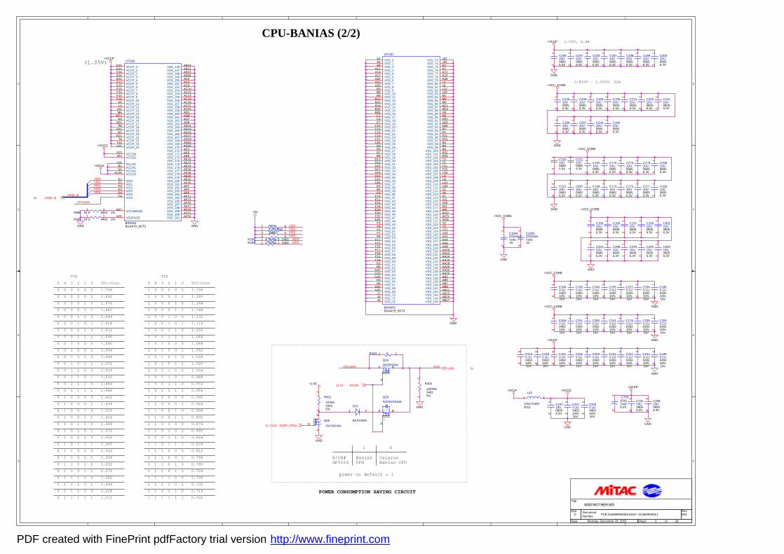
5
5
4
4
3
3
2
2
1
1
D D
C C
B B
A A
1.05V, 2.4A
0.844V ~ 1.356V, 32A
CPU-BANIAS (2/2)
(1.05V)
1
0
1.004
1
1
0
1
0
11
0
1
0
0
1.548
1
0
0
1
01.660
1
0
0.924
0
1
0
1
0
1
0
1
1.164
0
0
0
1
1.612
1
0
1
0
1
00
0
0
1
0
0.716
10
0
0.780
0
0 0.876
0
1
0
1
00
1.580
0
1.484
1
1
0
3
0
1
0
0
1
1
0
1.532
1
1
0
1
10
5
0
1
1
1
1
1
1
1
1.212
0
00
1
0
0
1
1
0
1
1
0
0
1
0
50
1
0
1
0
4
0
0
1
0
0
11
0
0
1
1
0.940
1
0.7640
1
0
1
0
1
1
0
1.516
1
0
1
0
0
0
0
1.596
1
1.564
1
0
0
0
1
1
1
1
0
1 1
0
0
1
0
0
0
1
0
0.908
1
1
0
1
0
0.972
0
0
1.260
11
1
0
0
0
1.020
1
1
0
1.356
0
1
0
0
0
20
0
1
1
1
0
1
0
0
0.812
0
1.388
11
1.116
00
1
1
1
0
0
1
1
1
0
1
1
0.860
1
1
1.436
10
1
0
1
1
1.420
1.100
1
1
1
0
1
1
0
0
0
0
0
0
1
VID VID
1
0
0
1
1.500
0
0
0
1
0
1
0
0
0
0
1.452
0
1
1.180
1
1
1
1
1
1
1
0
0
0
1
1.292
0
0
0
0
1
1.132
1.468
0
1
1
1
0
1
1
0
0
1.196
1.036
1.244
1.628
0
1
1
1
4
0
0.796
1
0
0
1
0
1
1.372
0.956
1
0
1
1.324
1
0
1
1
1
1
1
10
1
1
1
1
0
0
1
0.988
0
0
1
1
0.828
1.148
VCC-Core
0
0
1
1
1
0
1
1
0
1
0
0
0.732
0
0
0
0
0.700
1.676
1.228
1
1
1.068
0
0
1
1
1
0
0.844
0
1
1
0
1
1
1
1
0
0.892
1
1
0
1
0.748
1
0
0
0
1
1
1.340
1
1
0
0
1
0
0
0
11
00
00
0
0
0
1.276
1
1.084
1
00
1
0
0
1.692
1 0
0
1
1
1
1.0520
0
1
1.644
10
1.308
1
0
3
1
1
1
1
0
0
1
1
1.404
0
1
VCC-Core
1
0
1
2
0
1.708
0
0
0
1
1
1
B/CB#GPIO16
BaniasCPU
CeleronBanias CPU
power on default = 1
1 0
POWER CONSUMPTION SAVING CIRCUIT
PCB 316680900001/ASSY 411680900011 R01
8050 MOTHER B/D
C
3 34Monday, December 29, 2003
Title
Size DocumentNumber
Rev
Date: Sheet of
VID0
VID2VID3
VID1
VID5
VID3VID4
VID[0..4]
VID0VID1
VID4
VID2
CPUVID5 VID5
CPUVID5VID[0..4]31
STOP_CPU#11,13,31
B/CB#13,24
VID5 31
GND
GND
+VCCP
+VCC_CORE
GND
GND
+VCC_CORE
GND
+VCC_CORE
GND
GND
+VCC_CORE
+VCC_CORE
+VCCP
GND
+VCCA
+VCCP
+VCCQ
GND
+VCCP
GND
GND
+VCCQ+VCCP
GND
+5V
GND
+VCC_CORE
GND
GND
+1.5V
C20910U
6.3V0805
12
R193 01 2
R298 4.7K/NA 04021 2
C2220.1U0402
16V10%
12
C2480.1U0402
16V10%
12
C27910U
6.3V0805
12
C24910U
6.3V0805
12
C83110U
6.3V0805
12
C18710U
6.3V0805
12
C1910.1U0402
16V10%
12
U713C
BANIASBGA479_SKT3
A2A5A8
A11A14A17A20A23A26B3B6B9
B12B16B19B22B25C1C4C7
C10C13C15C18C21C24D2D5D7D9
D11D13D15D17D19D21D23D26
E3E6E8
E10E12E14E16E18E20E22E25
F1F4F5F7F9
F11F13F15F17F19F21F24G2G6
G22G23G26
H3H5
H21H25
J1J4J6
J22J24K2K5K21K23K26L3L6L22L25M1M4M5M21M24N3N6N22N23N26P2P5P21P24R1R4R6R22R25T3T5T21T23T26U2U6U22U24V1V4V5V21V25W3W6W22W23W26Y2Y5Y21Y24AA1AA4AA6AA8AA10AA12AA14AA16AA18AA20AA22AA25AB3AB5AB7AB9AB11AB13AB15AB17
VSS_0VSS_1VSS_2VSS_3VSS_4VSS_5VSS_6VSS_7VSS_8VSS_9VSS_10VSS_11VSS_12VSS_13VSS_14VSS_15VSS_16VSS_17VSS_18VSS_19VSS_20VSS_21VSS_22VSS_23VSS_24VSS_25VSS_26VSS_27VSS_28VSS_29VSS_30VSS_31VSS_32VSS_33VSS_34VSS_35VSS_36VSS_37VSS_38VSS_39VSS_40VSS_41VSS_42VSS_43VSS_44VSS_45VSS_46VSS_47VSS_48VSS_49VSS_50VSS_51VSS_52VSS_53VSS_54VSS_55VSS_56VSS_57VSS_58VSS_59VSS_60VSS_61VSS_62VSS_63VSS_64VSS_65VSS_66VSS_67VSS_68VSS_69VSS_70VSS_71VSS_72
VSS_73VSS_74VSS_75VSS_76VSS_77VSS_78VSS_79VSS_80VSS_81VSS_82VSS_83VSS_84VSS_85VSS_86VSS_87VSS_88VSS_89VSS_90VSS_91VSS_92VSS_93VSS_94VSS_95VSS_96VSS_97VSS_98VSS_99
VSS_100VSS_101VSS_102VSS_103VSS_104VSS_105VSS_106VSS_107VSS_108VSS_109VSS_110VSS_111VSS_112VSS_113VSS_114VSS_115VSS_116VSS_117VSS_118VSS_119VSS_120VSS_121VSS_122VSS_123VSS_124VSS_125VSS_126VSS_127VSS_128VSS_129VSS_130VSS_131VSS_132VSS_133VSS_134VSS_135VSS_136VSS_137VSS_138VSS_139VSS_140VSS_141VSS_142VSS_143VSS_144VSS_145
C17510U
6.3V0805
12
C25010U
6.3V0805
12
C18310U
6.3V0805
12
C2660.1U0402
16V10%
12
D14
BAT54/NA
1 3
C2010.1U0402
16V10%
12
C2510.1U0402
16V10%
12
C29610U
6.3V0805
12
C2360.1U0402
16V10%
12
+ C1004220U/NA73434V
12
RP284.7K*4/NA1206
1234
8765
L41
120Z/100M2012
1 2
C24010U
6.3V0805
12
C19310U
6.3V0805
12
C17910U
6.3V0805
12
C15510U
6.3V0805
12
C80710U
6.3V0805
12
C19010U
6.3V0805
12
C17710U
6.3V0805
12
C1810.1U0402
16V10%
12
C2420.1U0402
16V10%
12
C32010U
6.3V0805
12
C23010U
6.3V0805
12
C2350.1U0402
16V10%
12
C19910U
6.3V0805
12
+ C1005220U/NA73434V
12
C18810U
6.3V0805
12
C19210U
6.3V0805
12
C1950.1U0402
16V10%
12
U713D
BANIASBGA479_SKT3
AD1
AC8AC10AC12AC14AC16AC18AC21AC24
E2F2F3G3G4H4
D10D12D14D16E11E13E15F10F12F14F16K6L5
L21M6
M22N5
N21P6
P22R5
R21T6
T22
P23W4
AE7
F26B1N1
AC5AC2AB26AB23AB21AB19
AD4AD7AD9AD11AD13
U21
AE8AE6AE3AD25AD22AD19AD17AD15
AE10AE12AE14AE16AE18AE20AE23AE26AF2AF5AF9AF11AF13AF15AF17AF19AF21
AF6 AF24
AC26
VSS_160
VSS_152VSS_153VSS_154VSS_155VSS_156VSS_157VSS_158VSS_159
VID0VID1VID2VID3VID4VID5
VCCP_0VCCP_1VCCP_2VCCP_3VCCP_4VCCP_5VCCP_6VCCP_7VCCP_8VCCP_9VCCP_10VCCP_11VCCP_12VCCP_13VCCP_14VCCP_15VCCP_16VCCP_17VCCP_18VCCP_19VCCP_20VCCP_21VCCP_22VCCP_23
VCCQ0VCCQ1
VCCSENSE
VCCA0VCCA1VCCA2
VSS_151VSS_150VSS_149VSS_148VSS_147VSS_146
VSS_161VSS_162VSS_163VSS_164VSS_165
VCCP_24
VSS_173VSS_172VSS_171VSS_170VSS_169VSS_168VSS_167VSS_166
VSS_174VSS_175VSS_176VSS_177VSS_178VSS_179VSS_180VSS_181VSS_182VSS_183VSS_184VSS_185VSS_186VSS_187VSS_188VSS_189VSS_190
VSSENSE VSS_191
VCCA3
C1940.1U0402
16V10%
12
R899 54.9 0402 1%1 2
C25410U
6.3V0805
12
C15610U
6.3V0805
12
C25610U
6.3V0805
12
C31210U
6.3V0805
12
R885 54.9 0402 1%1 2
C23110U
6.3V0805
12
C27010U
6.3V0805
12
+C768
150U73436.3V
12
C24110U
6.3V0805
12
C32110U
6.3V0805
12
C21410U
6.3V0805
12
C2680.1U0402
16V10%
12
R299 4.7K/NA 04021 2
C2800.1U0402
16V10%
12
C18910U
6.3V0805
12
DSG
Q28SI2301DS/NA
G
DS
C23710U
6.3V0805
12
C1960.1U0402
16V10%
12
DS
Q45
2N7002/NAG
DS
C19810U
6.3V0805
12
C15710U
6.3V0805
12
C1780.1U0402
16V10%
12
C25710U
6.3V0805
12
C3190.1U0402
16V10%
12
C16810U
6.3V0805
12
DS
Q162N7002/NA
G
DS
C25810U
6.3V0805
12
C18010U
6.3V0805
12
C20310U
6.3V0805
12
C2590.1U0402
16V10%
12
C2000.1U0402
16V10%
12
C1850.1U0402
16V10%
12
R400
10K/NA04025%1
2
C2040.1U0402
16V10%
12
C2650.1U0402
16V10%
12
C26410U
6.3V0805
12
C15810U
6.3V0805
12
C22010U
6.3V0805
12
C1820.1U0402
16V10%
12
C17310U
6.3V0805
12
C3180.1U0402
16V10%
12
C26710U
6.3V0805
12
R401
1K/NA04025%1
2
C22610U
6.3V0805
12
C1860.1U0402
16V10%
12
PDF created with FinePrint pdfFactory trial version http://www.fineprint.com
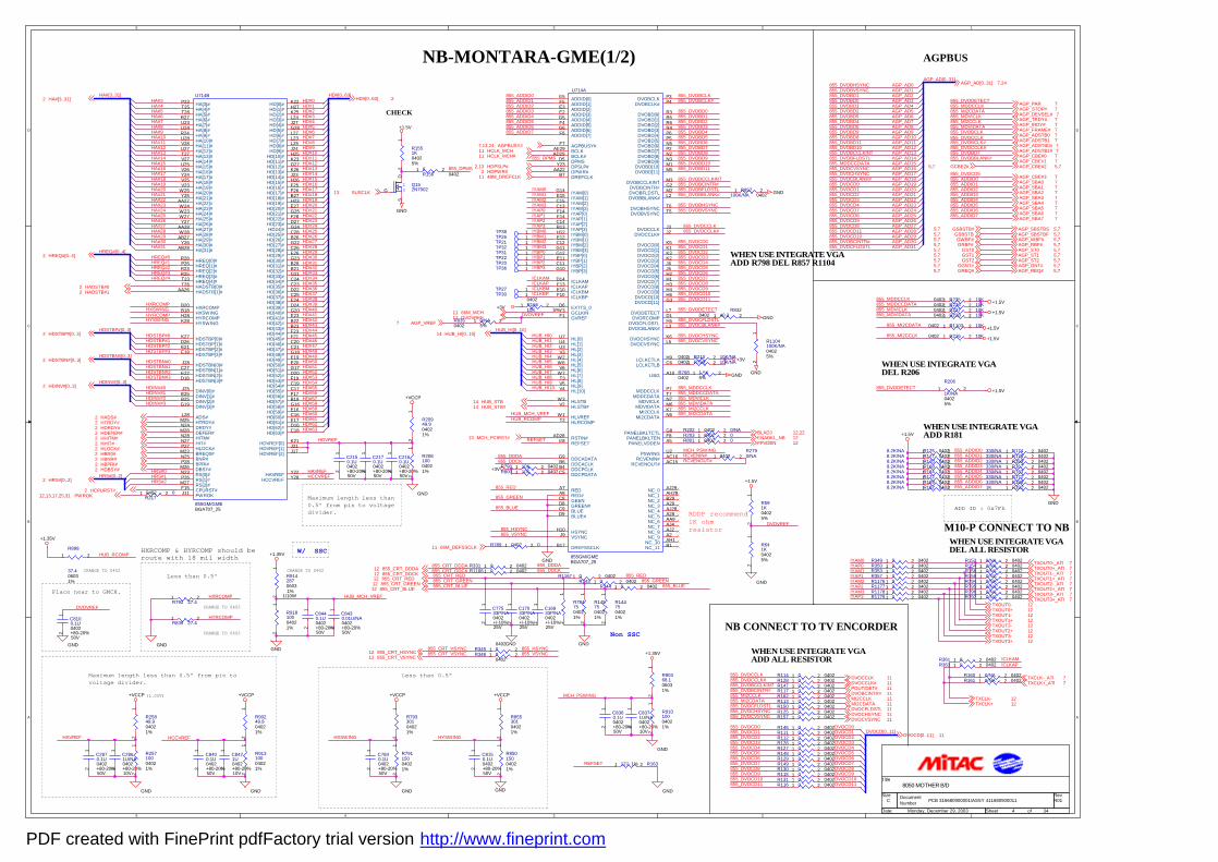
5
5
4
4
3
3
2
2
1
1
D D
C C
B B
A A
Maximum length less than0.5" from pin to voltagedivider.
Maximum length less than 0.5" from pin tovoltage divider.
Less than 0.5"
Less than 0.5"
(1.05V)
Place near to GMCH.
Non SSC
W/ SSCHXRCOMP & HYRCOMP should beroute with 18 mil width
NB-MONTARA-GME(1/2)
CHANGE TO 0402
CHANGE TO 0402
CHANGE TO 0402CHANGE TO 0402
ADD ID : 0x7Fh
CHECK
AGPBUS
NB CONNECT TO TV ENCORDER
WHEN USE INTEGRATE VGAADD ALL RESISTOR
M10-P CONNECT TO NBWHEN USE INTEGRATE VGADEL ALL RESISTOR
WHEN USE INTEGRATE VGAADD R181
WHEN USE INTEGRATE VGAADD R798 DEL R857 R1104
RDDP recommend1K ohmresistor
WHEN USE INTEGRATE VGADEL R206
PCB 316680900001/ASSY 411680900011 R01
8050 MOTHER B/D
C
4 34Monday, December 29, 2003
Title
Size DocumentNumber
Rev
Date: Sheet of
HA#[3..31] HD#[0..63]
HREQ#[0..4]
HDINV#[0..3]
HDSTBN#[0..3]
HDSTBP#[0..3]
HRS#[0..2]
HA#3HA#4HA#5HA#6
HA#9
HA#7
HA#10
HA#8
HA#13
HA#11
HA#14
HA#12
HA#17
HA#15
HA#18
HA#16
HA#21
HA#19
HA#22
HA#20
HA#25
HA#23
HA#26
HA#24
HA#29
HA#27
HA#30
HA#28
HA#31
HD#0HD#1
HD#3HD#2
HD#5HD#6
HD#4
HD#7
HD#12
HD#15HD#14HD#13
HD#9HD#10
HD#8
HD#11
HD#20
HD#31
HD#23HD#22
HD#24
HD#29
HD#21
HD#17HD#18
HD#27HD#28
HD#16
HD#19
HD#25
HD#30
HD#26
HD#36
HD#47
HD#39HD#38
HD#40
HD#45
HD#37
HD#33HD#34
HD#43HD#44
HD#32
HD#35
HD#41
HD#46
HD#42
HD#52
HD#63
HD#55HD#54
HD#56
HD#61
HD#53
HD#49HD#50
HD#59HD#60
HD#48
HD#51
HD#57
HD#62
HD#58
HREQ#0HREQ#1HREQ#2HREQ#3HREQ#4
HDINV#0HDINV#1HDINV#2HDINV#3
HDSTBP#0HDSTBP#1HDSTBP#2HDSTBP#3
HDSTBN#0HDSTBN#1
HDSTBN#3HDSTBN#2
HRS#0HRS#1HRS#2
HDVREF
HAVREFHCCVREF
HAVREF HCCVREF
HXRCOMPHXSWINGHYRCOMPHYSWING
HXRCOMP
HYRCOMP
HXSWING HYSWING
HUB_RCOMP
REFSET
HUB_RCOMP
HUB_HI8
HUB_MCH_VREF
MCH_PSWING
HUB_HI[0..10]
HUB_HI1
HUB_HI4
HUB_HI10HUB_HI9
855_DPMS
HUB_HI5
855_DVOCBLANK#
HUB_MCH_VREF
855_DVODETECT
HUB_HI0
HUB_HI6
MCH_PSWING
HUB_HI2
HUB_HI7
855_DVOBFLDSTL
REFSET
HUB_HI3
RCVENOUT#RCVENIN#
855_MDVIDATA
855_DVODETECT855_MDDCCLK
855_DVOCD5
855_DVOBCLK
855_DVOBD7
855_MI2CDATA
855_DVOCCLK
855_MDVICLK
855_ADDID5855_ADDID6
855_ADDID0
855_ADDID3855_ADDID2
855_DVOBCLK855_DVOBCLK#
855_DVOBD0855_DVOBD1855_DVOBD2855_DVOBD3855_DVOBD4855_DVOBD5855_DVOBD6855_DVOBD7855_DVOBD8
855_DVODETECT
855_ADDID0855_ADDID1855_ADDID2855_ADDID3855_ADDID4855_ADDID5
855_ADDID7855_ADDID6
855_DVOCCLK855_DVOCCLK#
855_DVOBCCLKINT
855_MDDCCLK855_MDDCCDATA855_MDVICLK855_MDVIDATA855_MI2CCLK855_MI2CDATA
855_DVOCHSYNC855_DVOCVSYNC
855_DVOBBLANK#
855_DVOBHSYNC855_DVOBVSYNC
855_DVOCD4
855_DVOCD2
855_DVOCD8
855_DVOCD1
855_DVOCD9
855_DVOCD3
855_DVOCD6
855_DVOCD0
855_DVOCD10
855_DVOCD7
855_DVOCD5
855_DVOCD11
855_DPMS
IYAM0IYAM1IYAM2IYAM3IYAP0IYAP1IYAP2IYAP3IYBM0IYBM1IYBM2IYBM3IYBP0IYBP1IYBP2IYBP3
ICLKAMICLKAPICLKBMICLKBP
855_CRT_BLUE855_CRT_GREEN
855_DVOBD10855_DVOBD11
855_MI2CCLK
855_DVOBBLANK#
855_ADDID1
855_ADDID4
855_ADDID7
855_DVOCCLK#855_DVOBCLK#
855_DDDA
855_BLUE
855_DVOBCINTR#
855_DVOBD9
855_ADDID4855_ADDID3
855_ADDID0
855_ADDID2
855_ADDID5
855_ADDID7
855_ADDID1
855_ADDID6
855_MDDCCDATA855_MDVICLK855_MDVIDATA
855_MDDCCLK
855_MI2CDATA
855_DVOCD5
855_DVOBCCLKINT855_DVOBCINTR#
855_DVOCD10
855_DVOCD2
855_DVOCD8
855_DVOCCLK#
855_DVOCD0855_DVOCD1
855_DVOCFLDSTL
855_DVOCD11
855_DVOCD4
855_DVOCCLK
855_DVOCD7
855_DVOCVSYNC855_DVOCHSYNC
855_DVOCD3
855_DVOCD6
855_MI2CCLK
855_DVOCD9
855_DVOCVSYNC AGP_AD16
AGP_AD11855_DVOBD11
AGP_AD7855_DVOBD4
AGP_AD4855_DVOBD3
AGP_AD26855_DVOCD9
AGP_AD24855_DVOCD7
DVOCD4
855_DVOCD1 AGP_AD20
855_DVOBFLDSTL AGP_AD14
855_DVOBD1 AGP_AD2
AGP_AD19855_DVOCD0
AGP_AD10855_DVOBD8
855_DVOBD6 AGP_AD8
855_DVOCD10 AGP_AD29
DVOCD5
DVOCD7
DVOCD0
AGP_AD23855_DVOCD4AGP_AD22855_DVOCD3
AGP_AD3855_DVOBD0
AGP_AD30855_DVOBCINTR#
AGP_AD1855_DVOBVSYNC
855_DVOCHSYNC AGP_AD17
AGP_AD5855_DVOBD2
DVOCD11
AGP_AD28855_DVOCD11
855_DVOCD6 AGP_AD25
DVOCD6
DVOCD9
AGP_AD[0..31]
855_MDDCCDATA AGP_AD15
AGP_AD13855_DVOBCCLKINT
855_DVOBD5 AGP_AD6
AGP_AD21855_DVOCD2
855_DVOCFLDSTL
DVOCD[0..11]
AGP_AD0855_DVOBHSYNC
855_DVOCD8 AGP_AD27
DVOCD1DVOCD2
DVOCD10
AGP_AD12855_DVOBD10
DVOCD8
AGP_AD31855_DVOCFLDSTL
AGP_AD9855_DVOBD9
AGP_AD18855_DVOCBLANK#
DVOCD3
DVOVREF
DVOVREF
DVOVREF
855_MI2CCLK
855_MI2CDATA
IYAM3
IYAM1IYAP1
IYAP0
IYAP3
IYAM2IYAP2
IYAM0
ICLKAMICLKAP
855_RED
855_GREEN
855_HSYNC855_VSYNC
855_CRT_RED855_CRT_DDCK855_CRT_DDDA
855_DDCK
855_DDDA855_DDCK
855_BLUE
855_RED855_GREEN
855_CRT_VSYNC855_CRT_HSYNC 855_HSYNC
855_VSYNC
HA#[3..31]2
HREQ#[0..4]2
HADSTB#02HADSTB#12
HDSTBP#[0..3]2
HDSTBN#[0..3]2
HDINV#[0..3]2
HADS#2HTRDY#2HDRDY#2HDEFER#2HHITM#2
HLOCK#2HHIT#2
HBR0#2HBNR#2
HDBSY#2HBPRI#2
HRS#[0..2]2
HCPURST#2PWROK12,13,17,25,31
HD#[0..63] 2
DVOVREF11
HDPWR#2HDPSLP#2,13
HUB_STB14
AGPBUSY#7,13,24
48M_DREFCLK11
HUB_HI[0..10]14
HUB_STB#14
HCLK_MCH11
66M_MCH11
MCH_PCIRST#13
HCLK_MCH#11
BLADJ 12,22
FPVDEN 12ENABKL_NB 12
AGP_CBE#1 7
AGP_TRDY# 7
AGP_ADSTB0 7
AGP_STOP# 7
AGP_FRAME# 7
AGP_DEVSEL# 7
AGP_CBE#0 7
AGP_ADSTB1 7
AGP_PAR 7
AGP_CBE#3 7
AGP_CBE#2 5,7
AGP_IRDY# 7
AGP_SBA0 7
AGP_SBA6 7
AGP_SBA4 7
AGP_SBA1 7AGP_SBA2 7
AGP_SBA5 7
AGP_SBA3 7SUSCLK13
TXCLK+ 12TXCLK- 12
GCBE2#5,7
GSBSTB#5,7GSBSTB5,7GWBF#5,7GRBF#5,7
GST05,7GST15,7GST25,7
AGP_SBA7 7
AGP_SBSTBS 5,7AGP_SBSTBF 5,7AGP_WBF# 5,7AGP_RBF# 5,7AGP_ST0 5,7AGP_ST1 5,7AGP_ST2 5,7
GGNT#5,7GREQ#5,7
AGP_GNT# 5,7AGP_REQ# 5,7
TXOUT3-_ATI 7TXOUT2+_ATI 7
TXOUT0+_ATI 7
TXOUT1+_ATI 7
TXOUT3+_ATI 7
TXOUT0-_ATI 7
TXOUT2-_ATI 7
TXOUT1-_ATI 7
AGP_ADSTB0# 7AGP_ADSTB1# 7
AGP_AD[0..31] 7,24
AGP_VREF7
POUT/DET# 11
DVOCCLK 11
MI2CCLK 11
DVOCVSYNC 11
DVOBCINTR# 11
DVOCCLK# 11
DVOCFLDSTL 11MI2CDATA 11
DVOCHSYNC 11
DVOCD[0..11] 11
TXOUT3- 12
TXOUT0- 12
TXOUT1+ 12TXOUT2- 12TXOUT2+ 12
TXOUT3+ 12
TXOUT0+ 12TXOUT1- 12
TXCLK-_ATI 7TXCLK+_ATI 7
855_CRT_RED12
855_CRT_BLUE12855_CRT_GREEN12
855_CRT_DDCK12855_CRT_DDDA12
855_CRT_HSYNC12855_CRT_VSYNC12
66M_DEFSSCLK11
+VCCP
GND
GND
+VCCP
GND
+VCCP
GND
GND
+VCCP +VCCP
GND
+1.35V
GND
+1.35V
+1.35V
GND
GND
GND
+3V
GND
+3V
GNDGND
+3V
GND
GND
+1.5V
GND
GND GND
+1.5V
+1.5V
+1.5V
+1.5V
GND
+1.5V
+1.5V
+1.5V
GND
R203 004021 2
TP21 1
R188330/NA 04021 2
R1560
04021 2
C8371U/NA0402
10V+80-20%
12
R20949.904021%
12
R1103 10K0402 1 2
R202 0/NA04021 2
R1447504021%
12
C2861U/NA0402
10V+80-20%
12
R800 10K 04021 2
R148 0 04021 2
R113 0 04021 2
R353 0 04021 2
R90368.106031%
12
R157 0 04021 2
R795 0/NA 04021 2
R130 0 04021 2
R361 0 04021 2
C8440.1U0402
50V+80-20%
12
TP32 1
R1688.2K/NA 04021 2
R1178 0 04021 2
C2870.1U0402
50V+80-20%
12
R801 004021 2
R789 004021 2
R344 0 04021 2
C8430.01U/NA0402
50V+80-20%
12
C8400.1U0402
50V+80-20%
12
R83240.20402 1 2
C8421U0402
10V+80-20%
12
R792 27.41 2
R1898.2K/NA 04021 2R1811K 04021 2
R1551K04025%
12
TP31 1
R235 10K04021 2
R147 0 04021 2
U714B
855GM/GMEBGA707_25
N27N28
P27
M25
B20B18H28K28
J11
K22H27K25L24J27G28L27L23L25J24H25K23G27K26J23H26F25F26B27H23E27G25F28D27G24C28B26G22C26E26G23B28B21G21C24C23D22C25E24D24G20E23B22B23F23F21C20C21G18E19E20G17D20F19C19C17F17B19G16E16C16E17D16C18
P23T25T28R27U23U24R24U28V28U27T27V27U25V26Y24V25V23
W25Y25
AA27W24W23W27Y27
AA28W28
AB27Y26
AB28
R28P25R23R25T23T26
AA26
J28C27E22D18
K27D26E21E18
K21J21J17
Y22Y28
J25E25B25G19
N23P26M27
L28
N25P28
M23
F15
M26
M28N24
HIT#HITM#
HLOCK#
HTRDY#
HXRCOMPHXSWINGHYRCOMPHYSWING
PWROK
HD[0]#HD[1]#HD[2]#HD[3]#HD[4]#HD[5]#HD[6]#HD[7]#HD[8]#HD[9]#
HD[10]#HD[11]#HD[12]#HD[13]#HD[14]#HD[15]#HD[16]#HD[17]#HD[18]#HD[19]#HD[20]#HD[21]#HD[22]#HD[23]#HD24]#
HD[25]#HD[26]#HD[27]#HD[28]#HD[29]#HD[30]#HD[31]#HD[32]#HD[33]#HD[34]#HD[35]#HD[36]#HD[37]#HD[38]#HD[39]#HD[40]#HD[41]#HD[42]#HD[43]#HD[44]#HD[45]#HD[46]#HD[47]#HD[48]#HD[49]#HD[50]#HD[51]#HD[52]#HD[53]#HD[54]#HD[55]#HD[56]#HD[57]#HD[58]#HD[59]#HD[60]#HD[61]#HD[62]#HD[63]#
HA[3]#HA[4]#HA[5]#HA[6]#HA[7]#HA[8]#HA[9]#HA[10]#HA[11]#HA[12]#HA[13]#HA[14]#HA[15]#HA[16]#HA[17]#HA[18]#HA[19]#HA[20]#HA[21]#HA[22]#HA[23]#HA[24]#HA[25]#HA[26]#HA[27]#HA[28]#HA[29]#HA[30]#HA[31]#
HREQ[0]#HREQ[1]#HREQ[2]#HREQ[3]#HREQ[4]#HADSTB[0]#HADSTB[1]#
HDSTBN[0]#HDSTBN[1]#HDSTBN[2]#HDSTBN[3]#
HDSTBP[0]#HDSTBP[1]#HDSTBP[2]#HDSTBP[3]#
HDVREF[0]HDVREF[1]HDVREF[2]
HAVREFHCCVREF
DINV[0]#DINV[1]#DINV[2]#DINV[3]#
RS[0]#RS[1]#RS[2]#
ADS#
BNR#BPRI#
BREQ0#
CPURST#
DBSY#
DEFER#DRDY#
R114 0 04021 2
R112 0 04021 2
R210 10K/NA04021 2
R7847504021%
12
R1457504021%
12
R797 0/NA 04021 2
R161 0/NA 04021 2
R91428706031%
1/10W
12
R131 0 04021 2
R169330/NA 04021 2
C8100.1U0402
50V+80-20%
12
R1176 0 04021 2
R16610K
0402
5%1 2
C8360.1U0402
50V+80-20%
12
TP22 1
R348 00402
1 2
R1778.2K/NA 04021 2
R1828.2K/NA 04021 2
R91810004021%
12
R125 0 04021 2
R126 0 04021 2
R150 0 04021 2
R79115004021%
12
C2150.1U0402
50V+80-20%
12
R206
1K/NA04025%
1 2
TP20 1
R796 0/NA 04021 2
R116 0 04021 2
R357 0 04021 2
R1848.2K/NA 04021 2
R236 10K04021 2
R154 0/NA 04021 2
R111 0 04021 2
R591K04025%
12
R79330104021%
12
R1166 0 04021 2
C2170.1U0402
50V+80-20%
12
TP38 1
TP36 1
R345 00402
1 2
R174330/NA 04021 2
C17033P/NA0402
25V+/-10%
12
R91010004021%
12
R128 0 04021 2
R1728.2K/NA 04021 2
R176330/NA 04021 2
R85015004021%
12
R898
37.406031%
1 2
R1104100K/NA04025%
12
R349 0 04021 2
R794 0/NA 04021 2R1177 0 04021 2
R1758.2K/NA 04021 2
C7840.1U0402
50V+80-20%
12
R149 0 04021 2
C2160.1U0402
50V+80-20%
12
R227 10K04021 2
R25710004021%
12
DS
Q152N7002G
DS
R217004021 2
R85530104021%
12
C8150.1U0402
50V+80-20%
12
R835 0/NA0402 5%
1 2
R127 0 04021 2
R159 0/NA 04021 2
R857100K/NA 0402
1 2
TP27 1
R153 0/NA 04021 2
R25849.904021%
12
R1167 0 04021 2
R798 1.5K0402 5%
1 2
R117 0 04021 2
R183330/NA 04021 2
R160 0/NA 04021 2
R1708.2K/NA 04021 2
C77533P/NA0402
25V+/-10%
12
R799 10K/NA04021 2
TP30 1
R226 10K04021 2
C16933P/NA0402
25V+/-10%
12
R91310004021%
12
R171330/NA 04021 2
R350 0 04021 2R331 0 04021 2
R129 0 04021 2
R158 0/NA 04021 2
R146 0 04021 2
R90249.904021%
12
TP26 1
R162 0 04021 2
R641K04025%
12
U714A
855GM/GMEBGA707_25
E5F5E3E2G5F4G6F6
F7AE29AD29
C9D9
B6G9
B4C5
D5Y23
AA22B7
L2
M3G2
B17
K5K1K3K2J6J5H2H1H3H4H6G3
H5
K6L5
L7D1
C8D8
H10
A7A8
U7U4U3V3
W2W6V6
W7T3V5V4
R3R5R6R4P6P5N5P2N2N3M1M5
M2
T6T5
L3
J3J2
G14E15C15C13F14E14C14B13H12E12C12G11G12E11C11G10
H9C6
A10
G8F8A5
U2AC16AC15
AD28
D6Y3F1
T2
W3V2
W1
D14E13E10F10
P7T7N7M6K7N6
E8
AJ29AH29B29A29AJ28A28AA9AJ4AJ2A2AH1B1
P4P3
J9
ADDID[0]ADDID[1]ADDID[2]ADDID[3]ADDID[4]ADDID[5]ADDID[6]ADDID[7]
AGPBUSY#BCLKBCLK#
BLUEBLUE#
DDCACLKDDCADATA
DDCPCLKDDCPDATA
DPMSDPSLP#DPWR#DREFCLK
DVOBBLANK#
DVOBCCLKINTDVOBCINTR#
DREFSSCLK
DVOCD[0]DVOCD[1]DVOCD[2]DVOCD[3]DVOCD[4]DVOCD[5]DVOCD[6]DVOCD[7]DVOCD[8]DVOCD[9]
DVOCD[10]DVOCD[11]
DVOCFLDSTL
DVOCHSYNCDVOCVSYNC
DVODETECTDVORCOMP
GEENGREEN#
HSYNC
REDRED#
HL[0]HL[1]HL[2]HL[3]HL[4]HL[5]HL[6]HL[7]HL[8]HL[9]HL[10]
DVOBD[0]DVOBD[1]DVOBD[2]DVOBD[3]DVOBD[4]DVOBD[5]DVOBD[6]DVOBD[7]DVOBD[8]DVOBD[9]
DVOBD[10]DVOBD[11]
DVOBFLDSTL
DVOBHSYNCDVOBVSYNC
DVOCBLANK#
DVOCCLKDVOCCLK#
IYAM[0]IYAM[1]IYAM[2]IYAM[3]IYAP[0]IYAP[1]IYAP[2]IYAP[3]IYBM[0]IYBM[1]IYBM[2]IYBM[3]IYBP[0]IYBP[1]IYBP[2]IYBP[3]
LCLKCTLALCLKCTLB
LIBG
PANELBKLTCTLPANELBKLTENPANELVDDEN
PSWINGRCVENIN#
RCVENOUT#
RSTIN#
EXTTS_0GCLKINGVREF
HLRCOMP
HLSTBHLSTB#
HLVREF
ICLKAMICLKAPICLKBMICLKBP
MDDCCLKMDDCDATA
MDVICLKMDVIDATA
MI2CCLKMI2CDATA
REFSET
NC_0NC_1NC_2NC_3NC_4NC_5NC_6NC_7NC_8NC_9
NC_10NC_11
DVOBCLK#DVOBCLK
VSYNC
R839 27.41 2
R115 0 04021 2
R363 0 04021 2
R167330/NA 04021 2
R2790/NA04021 2
R163127 1%1 2
R343 0 04021 2
R790 10K 04021 2
R20810004021%
12
R216 10K0402 1 2
R1179 0 04021 2
PDF created with FinePrint pdfFactory trial version http://www.fineprint.com
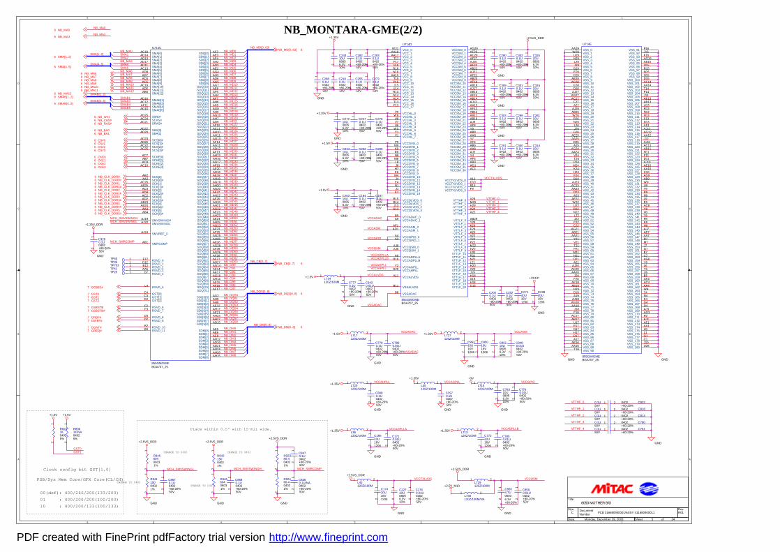
5
5
4
4
3
3
2
2
1
1
D D
C C
B B
A A
Place within 0.5" with 15-mil wide.
Clock config bit GST[1,0]
PSB/Sys Mem Core/GFX Core(CL/CH)
00(def): 400/266/200(133/200)01 : 400/200/200(100/200)10 : 400/200/133(100/133)
NB_MONTARA-GME(2/2)
CHANGE TO 0402
CHANGE TO 0402
CHANGE TO 0402
CHANGE TO 0402
PCB 316680900001/ASSY 411680900011 R01
8050 MOTHER B/D
C
5 34Monday, December 29, 2003
Title
Size DocumentNumber
Rev
Date: Sheet of
SMAB[4..5]
NB_MA8
SMAB4SMAB5
MCH_SMRCOMP
MCH_SMRCOMP
VTTHF_0
VTTHF_1
VTTHF_2
VTTHF_3
VTTHF_4
VCCGPIO
VCCQSM
VCCADPLLA
GST0
NB_MA0
NB_MA3
VSSADAC
VCCGPIO
VCCAHPLL
VTTHF_2
VCCADAC
VTTHF_4
VCCTXLVDS
VCCASM
VTTHF_0
VCCADAC
VCCAGPLL
VCCADPLLB
VTTHF_3
VCCASM
VCCTXLVDS
VCCQSM
VTTHF_1
VCCAGPLL
VCCADPLLAVCCADPLLB
VCCAHPLL
VCCALVDS
NB_MD15
NB_MD40
NB_DQS5
NB_CB2
NB_MD8
NB_MD36
NB_MD30
SMA4
NB_MD20
NB_DM5
NB_DQS7
NB_MA3
NB_CB[0..7]NB_MD62
NB_MD54
NB_MD2
NB_MD56
NB_MD9
SMA[1..2]
NB_DM0
NB_DQS6
NB_DQS4
NB_CB1
NB_MD26
NB_MD22
NB_MA11
NB_MA6
NB_MD53
NB_MD3
NB_MD46
NB_MD43
NB_MD35
SMAB2
NB_MA12
NB_CB7
NB_DM7
NB_MD1
NB_DM3
NB_CB0
NB_MD51
NB_MD21
NB_MD10
NB_MD29
NB_MA10
NB_MD52
GST1
NB_DM1
MCH_SMVSWINGH
NB_MD42
NB_MD63
NB_MD57
NB_MD11
NB_MD4
NB_MD41
NB_MD34
NB_MD28
SMAB1SMAB[1..2]
NB_DM8
NB_DQS0
MCH_SMVSWINGL
NB_DM2
NB_MD50
NB_MD18
NB_MD16
NB_MA9
NB_MD49
NB_MD45
NB_MD5
MCH_SMVSWINGL
NB_MD38
NB_MD27
NB_DQS1
NB_MD24
NB_MD61
NB_CB5
NB_MD12
NB_MD39
NB_MA0NB_MD[0..63]
NB_MD23
NB_MD37
NB_DM[0..8]
NB_DQS[0..8]
NB_MD0
NB_CB4
NB_MD44
NB_MD13
NB_MD6
NB_MD47
NB_MD17
NB_DM4
MCH_SMVSWINGH
NB_DQS2
NB_CB6
NB_MD25
NB_MA7
SMA1
NB_MD55
NB_MD48
NB_MD60NB_MD59
NB_MD7
NB_MD33
SMA[4..5]
NB_CB3
NB_DM6
NB_DQS3
NB_MD14
NB_MD31
NB_MD19
SMA5
SMA2
NB_DQS8
NB_MD58
NB_MD32
VSSADAC
NB_MA06
NB_MA36
SMA[1..2]6
SMA[4..5]6
SMAB[1..2]6
SMAB[4..5]6
NB_WE#6NB_CAS#6NB_RAS#6
NB_BA06NB_BA16
CS#06CS#16CS#26CS#36
CKE06CKE16CKE26CKE36
NB_MD[0..63] 6
NB_CB[0..7] 6
NB_DQS[0..8] 6
NB_DM[0..8] 6
NB_MA66NB_MA76NB_MA86NB_MA96NB_MA106
NB_MA126NB_MA116
GCBE2#7
GST07GST17GST27
GSBSTB7GSBSTB#7
GRBF#7GWBF#7
GGNT#7GREQ#7
NB_CLK_DDR56
NB_CLK_DDR2#6
NB_CLK_DDR3#6
NB_CLK_DDR26
NB_CLK_DDR36
NB_CLK_DDR1#6NB_CLK_DDR16
NB_CLK_DDR06
NB_CLK_DDR4#6
NB_CLK_DDR5#6
NB_CLK_DDR46
NB_CLK_DDR0#6
GND GND
+2.5VS_DDR +2.5VS_DDR
GNDGND
GND
+1.25V_DDR
+2.5VS_DDR
GND
GND
+1.35V
GND
GND
GND GND
+1.35V
+1.35V
GND
+1.5V
GND
GND
GND
+1.35V
GND
+3V
GND
+2.5VS_DDR
GND
+1.35V +1.35V
GND
+2.5VS_DDR
GND
GND
GND
GND
GND
GND
+VCCP
+1.35V
+1.5V
+1.5V
+2.5VS_DDR
+1.5V +1.5V
GND
+1.5V
+2.5V_M10
C7810.1U 040250V +80-20%
1 2
C2320.1U0402
50V+80-20%
12
U714E
855GM/GMEBGA707_25
AA29W29U29N29L29J29
G29E29C29
AE28AC28
E28D28
AJ27AG27AC27
F27A27
AJ26AB26W26R26N26L26J26
G26AE25AA25
D25A25
AG24AA24
V24T24P24M24K24H24F24B24
AJ23AC23AA23
D23A23
AE22W22U22R22N22L22J22F22C22
AG21AB21AA21
Y21V21T21P21M21H21D21A21
AJ20AC20AA20
J20F20
AE19AB19
H19D19A19
AJ18AG18AA18
J18F18
AC17AB17
U17R17N17H17D17A17
AE16AA16
T16
P16J16F16AG15AB15U15R15N15H15D15AC14AA14T14P14J14AE13AB13U13R13N13H13F13D13A13AJ12AG12AA12J12AJ11AC11AB11H11F11D11
AE10AJ10
AA10C10AG9AB9W9U9T9R9N9L9E9AC8Y8V8T8P8K8H8AJ7AE7AA7R7M7J7G7E7C7AG6Y6L6Y5U5B5AE4AC4AA4W4T4N4K4G4D4AJ3AG3R2AJ1AE1AA1U1L1G1C1J10U26
VSS_0VSS_1VSS_2VSS_3VSS_4VSS_5VSS_6VSS_7VSS_8VSS_9VSS_10VSS_11VSS_12VSS_13VSS_14VSS_15VSS_16VSS_17VSS_18VSS_19VSS_20VSS_21VSS_22VSS_23VSS_24VSS_25VSS_26VSS_27VSS_28VSS_29VSS_30VSS_31VSS_32VSS_33VSS_34VSS_35VSS_36VSS_37VSS_38VSS_39VSS_40VSS_41VSS_42VSS_43VSS_44VSS_45VSS_46VSS_47VSS_48VSS_49VSS_50VSS_51VSS_52VSS_53VSS_54VSS_55VSS_56VSS_57VSS_58VSS_59VSS_60VSS_61VSS_62VSS_63VSS_64VSS_65VSS_66VSS_67VSS_68VSS_69VSS_70VSS_71VSS_72VSS_73VSS_74VSS_75VSS_76VSS_77VSS_78VSS_79VSS_80VSS_81VSS_82VSS_83VSS_84VSS_85VSS_86VSS_87VSS_88VSS_89VSS_90
VSS_91VSS_92VSS_93VSS_94VSS_95VSS_96VSS_97VSS_98VSS_99
VSS_100VSS_101VSS_102VSS_103VSS_104VSS_105VSS_106VSS_107VSS_108VSS_109VSS_110VSS_111VSS_112VSS_113VSS_114VSS_115VSS_116VSS_117VSS_118VSS_119VSS_120VSS_121VSS_122VSS_123VSS_124
VSS_125VSS_126
VSS_127VSS_128VSS_129VSS_130VSS_131VSS_132VSS_133VSS_134VSS_135VSS_136VSS_137VSS_138VSS_139VSS_140VSS_141VSS_142VSS_143VSS_144VSS_145VSS_146VSS_147VSS_148VSS_149VSS_150VSS_151VSS_152VSS_153VSS_154VSS_155VSS_156VSS_157VSS_158VSS_159VSS_160VSS_161VSS_162VSS_163VSS_164VSS_165VSS_166VSS_167VSS_168VSS_169VSS_170VSS_171VSS_172VSS_173VSS_174VSS_175VSS_176VSS_177VSS_178VSS_179VSS_180
L38120Z/100M
1 2
TP25 1
R92460.404021%
12
C2550.1U0402
50V+80-20%
12
C78310U
6.3V0805
10%
12
C8570.1U0402
50V+80-20%
12 C174
10U16V1206
12
L714120Z/100M
1 2
C32410U
6.3V0805
10%
12
C85210U16V1206
12
C2730.1U0402
50V+80-20%
12
C8320.1U 040250V +80-20%
1 2
C2970.1U0402
50V+80-20%
12
C2900.1U0402
50V+80-20%
12
C7850.01U0402
50V+80-20%
12
L717120Z/100M
1 2
C2930.1U0402
50V+80-20%
12
C3030.1U0402
50V+80-20%
12
R94215004021%
12
L45120Z/100M
1 2
L42120Z/100M
1 2L729120Z/100M
1 2
L727120Z/100M
1 2
C8580.1U0402
50V+80-20%
12
R94115004021%
12
C28110U
6.3V0805
10%
12
U714D
855GM/GMEBGA707_25
W21AA19AA17
T17P17U16R16N16
AA15T15P15J15U14R14N14H14T13P13
B15B14J13
G13
P9M9K9R8N8M8L8J8H7E6M4J4E4N1J1E1
V9W8U8V7U6
W5Y1V1
AJ8AJ6
A4A3
AG29AF29AC29AF27AJ25AF24AB22AJ21AF21AB20AF18AB18AJ17AB16AF15AB14AJ13AA13AF12AB12AA11AB10AJ9AF9Y9AB8AA8Y7AF6AB6AA6AJ5Y4AF3AB3AG1AC1
A12D10B10F9
B8
B11
AB29Y29K29F29A26V22T22P22M22H22U21R21N21L21H20A20J19H18A18H16G15
V29M29H29A24A22
B9A9
A6B16
Y2D29
A11
AF1AD1
VCC_0VCC_1VCC_2VCC_3VCC_4VCC_5VCC_6VCC_7VCC_8VCC_9VCC_10VCC_11VCC_12VCC_13VCC_14VCC_15VCC_16VCC_17
VCCDLVDS_0VCCDLVDS_1VCCDLVDS_2VCCDLVDS_3
VCCDVO_0VCCDVO_1VCCDVO_2VCCDVO_3VCCDVO_4VCCDVO_5VCCDVO_6VCCDVO_7VCCDVO_8VCCDVO_9VCCDVO_10VCCDVO_11VCCDVO_12VCCDVO_13VCCDVO_14VCCDVO_15
VCCHL_0VCCHL_1VCCHL_2VCCHL_3VCCHL_4VCCHL_5VCCHL_6VCCHL_7
VCCQSM_0VCCQSM_1
VCCGPIO_0VCCGPIO_1
VCCSM_0VCCSM_1VCCSM_2VCCSM_3VCCSM_4VCCSM_5VCCSM_6VCCSM_7VCCSM_8VCCSM_9
VCCSM_10VCCSM_11VCCSM_12VCCSM_13VCCSM_14VCCSM_15VCCSM_16VCCSM_17VCCSM_18VCCSM_19VCCSM_20VCCSM_21VCCSM_22VCCSM_23VCCSM_24VCCSM_25VCCSM_26VCCSM_27VCCSM_28VCCSM_29VCCSM_30VCCSM_31VCCSM_32VCCSM_33VCCSM_34VCCSM_35VCCSM_36
VCCTXLVDS_0VCCTXLVDS_1VCCTXLVDS_2VCCTXLVDS_3
VSSADAC
VSSALVDS
VTTLF_0VTTLF_1VTTLF_2VTTLF_3VTTLF_4VTTLF_5VTTLF_6VTTLF_7VTTLF_8VTTLF_9
VTTLF_10VTTLF_11VTTLF_12VTTLF_13VTTLF_14VTTLF_15VTTLF_16VTTLF_17VTTLF_18VTTLF_19VTTLF_20
VTTHF_0VTTHF_1VTTHF_2VTTHF_3VTTHF_4
VCCADAC_0VCCADAC_1
VCCADPLLAVCCADPLLB
VCCAGPLLVCCAHPLL
VCCALVDS
VCCASM_0VCCASM_1
C2520.1U0402
50V+80-20%
12
C3280.1U0402
50V+80-20%
12
C2820.1U0402
50V+80-20%
12
C8590.01U0402
50V+80-20%
12
C22710U
6.3V0805
10%
12
C8480.01U0402
50V+80-20%
12
C1970.1U0402
50V+80-20%
12
C23410U
6.3V0805
10%
12
C77210U16V1206
12
C3020.1U0402
50V+80-20%
12
C8180.1U 040250V +80-20%
1 2
C8460.1U/NA0402
50V+80-20%
12
L730120Z/100M/NA
1 2
C1710.01U0402
50V+80-20%
12
C7790.1U0402
50V+80-20%
12
C31410U
6.3V0805
10%
12
C2990.1U0402
50V+80-20%
12
U714C
855GM/GMEBGA707_25
F12D12B12AA5
L4
C4
F3
D3
C3
B3
F2
D2
C2
B2
D7
AD22AD20
AC24
AB2AA2
AC26AB25AC3AD4AC2AD2
AB23AB24AA3AB4
AC7AB7AC9
AC10
AD23AD26AC22AC25
AF2AE3AF4AH2AD3AE2AG4AH3AD6AG5AG7
AF5AE8
AH4AF7AH6AF8AG8AH9AG10AH7AD9AF10AE11AH10AH11AG13AF14AG11AD12AF13AH13AH16AG17AF19AE20AD18AE18AH18AG19AH20AG20AF22AH22AF20AH19AH21AG22AE23AH23AE24AH25AG23AF23AF25AG25AH26AE26
AF28AG28
AG26AF26AE27AD27AG14AE14AE17AG16AH14AE15AF16AF17
AG2AH5AH8AE12AH17AE21AH24AH27AD15
AC18AD14AD13AD17AD11AC13AD8AD7AC6AC5
AC19AD5AB5
AD16AC12AF11AD10
AB1
AJ24
AJ19AJ22
AC21
AD25
AE5AE6AE9AH12AD19AD21AD24AH28AH15
RSVD_0RSVD_1RSVD_2RSVD_3
RSVD_5
GST[0]
RSVD_7
RSVD_8
GST[1]
RSVD_11
RSVD_6
RSVD_9
GST[2]
RSVD_10
RSVD_4
SBA[0]SBA[1]
SCAS#
SCK[0]SCK[0]#SCK[1]SCK[1]#SCK[2]SCK[2]#SCK[3]SCK[3]#SCK[4]SCK[4]#SCK[5]SCK[5]#
SCKE[0]SCKE[1]SCKE[2]SCKE[3]
SCS[0]#SCS[1]#SCS[2]#SCS[3]#
SDQ[0]SDQ[1]SDQ[2]SDQ[3]SDQ[4]SDQ[5]SDQ[6]SDQ[7]SDQ[8]SDQ[9]
SDQ[10]
SDQ[12]SDQ[11]
SDQ[13]SDQ[14]SDQ[15]SDQ[16]SDQ[17]SDQ[18]SDQ[19]SDQ[20]SDQ[21]SDQ[22]SDQ[23]SDQ[24]SDQ[25]SDQ[26]SDQ[27]SDQ[28]SDQ[29]SDQ[30]SDQ[31]SDQ[32]SDQ[33]SDQ[34]SDQ[35]SDQ[36]SDQ[37]SDQ[38]SDQ[39]SDQ[40]SDQ[41]SDQ[42]SDQ[43]SDQ[44]SDQ[45]SDQ[46]SDQ[47]SDQ[48]SDQ[49]SDQ[50]SDQ[51]SDQ[52]SDQ[53]SDQ[54]SDQ[55]SDQ[56]SDQ[57]
SDQ[59]SDQ[58]
SDQ[60]SDQ[61]SDQ[62]SDQ[63]SDQ[64]SDQ[65]SDQ[66]SDQ[67]SDQ[68]SDQ[69]SDQ[70]SDQ[71]
SDQS[0]SDQS[1]SDQS[2]SDQS[3]SDQS[4]SDQS[5]SDQS[6]SDQS[7]SDQS[8]
SMA[0]SMA[1]SMA[2]SMA[3]SMA[4]SMA[5]SMA[6]SMA[7]SMA[8]SMA[9]SMA[10]SMA[11]SMA[12]
SMAB[1]SMAB[2]SMAB[4]SMAB[5]
SMRCOMP
SMVREF_0
SMVSWINGHSMVSWINGL
SRAS#
SWE#
SDM[0]SDM[1]SDM[2]SDM[3]SDM[4]SDM[5]SDM[6]SDM[7]SDM[8]
L715120Z/100M
1 2
L713120Z/100M
1 2
C8140.1U 040250V +80-20%
1 2
R94560406031%
12
C24310U
6.3V0805
10%
12
C32510U
6.3V0805
10%
12
R8221K04025%
12
C8470.1U0402
50V+80-20%
12
C2020.1U0402
50V+80-20%
12
C2910.1U0402
50V+80-20%
12
C1840.1U0402
50V+80-20%
12
C3090.1U0402
50V+80-20%
12
C85110U
6.3V0805
10%
12
C2050.1U0402
50V+80-20%
12
C26310U
6.3V0805
10%
12
C23810U16V1206
12
C3430.01U0402
50V+80-20%
12
C16610U16V1206
12
C7800.1U 040250V +80-20%
1 2
R8061K/NA04025%
12
TP40 1
L720120Z/100M
1 2
C27210U
6.3V0805
10%
12
C7770.1U0402
50V+80-20%
12
C8604.7U
6.3V0603
+80-20%1
2
C2760.1U0402
50V+80-20%
12
C7860.01U0402
50V+80-20%
12
C7760.01U0402
50V+80-20%
12
R92360.404021%
12
C2880.1U0402
50V+80-20%
12
TP35 1
C1760.01U0402
50V+80-20%
12
C85010U16V1206
12
C27110U16V1206
12
TP703 1
C2470.1U0402
50V+80-20%
12
C3000.1U0402
50V+80-20%
12
TP41 1
C8080.1U0402
50V+80-20%
12
C2180.1U0402
50V+80-20%
12
R94660406031%
12
C3010.1U0402
50V+80-20%
12
PDF created with FinePrint pdfFactory trial version http://www.fineprint.com
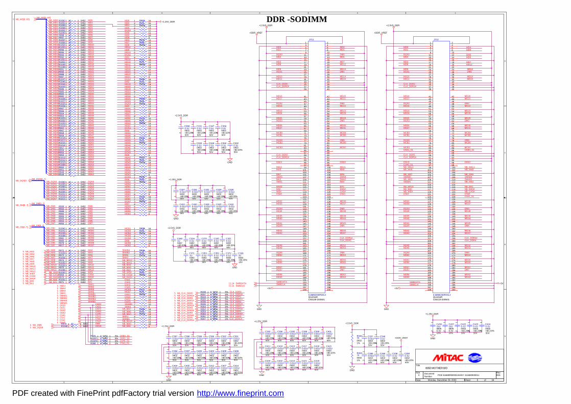
5
5
4
4
3
3
2
2
1
1
D D
C C
B B
A A
DDR -SODIMM
PCB 316680900001/ASSY 411680900011 R01
8050 MOTHER B/D
C
6 34Monday, December 29, 2003
Title
Size DocumentNumber
Rev
Date: Sheet of
MD45
MD25
MA8
MD30
SMBDATA
MD20
CAS#
MD57MD61DQS7
BA1
MD4
MD52
DQS8
DQS1
DM3
MD18
CLK_DDR3#
NB_BA1
MD36
NB_MA12
NB_WE#
MD45
MD52
MD35
DM8
CKE0
DM4
CKE2
MD20
NB_MA10
MCB0
MD38
DM8
NB_MA9
DM7
MD4
MA11
MD7
DQS3
CKE3
CLK_DDR1
RAS#
MD26
CLK_DDR3
MD39
MD6
DQS2
DM6
NB_CAS#
NB_MA3
DQS4MD38
DM7
MCB7
DM1
MD54
MD29
CLK_DDR1#
MCB7
SMA4
MD0
SMBCLK
MA6SMAB5
MD30
MD10
DM2
MD13
MD14
MD36
MD13
MD19
MD46
MD50
CLK_DDR5
MD3
MD23
DQS0
MD58
CS#2
MD23
MD9
MD32
DM0
MD62
SMAB4
DM6
NB_BA0
DM5
NB_RAS#
MD16
SMA2
DM2
MD2
MD42
DM1
CS#3
DM4
MD22
CS#1
NB_MA7 NB_MA6
MD22
DQS5MD41
MD51
MD61
DM0
MD48
DM3
CLK_DDR4
MD55
SMAB2
MCB3
MD46
MD29
MD54
DM5
MD55
CLK_DDR4#
MD14
MD62
MD39
MD7
MD6
MCB1
MD34
NB_MA11NB_MA8
MCB0
CKE1
CS#0
BA0
DQS5
DQS1
MD50
MD34
MD42
SMBDATA
MD26
SMA5
MD16
CLK_DDR0
MCB3
MD58
MD48
MD32
MD3
CLK_DDR0#
MD2
MD51
MA12
WE#
MD25
MA3
CLK_DDR2
MD35
MD18
MCB1
MA10
SMBCLK
DQS3
DQS7
MA9
MA7
DQS4
MD10
DQS8
MD41
DQS2
MD9
DQS0
MD19
MD57
MD0
MD0
MD3
MD6MD7MD8MD9MD10MD11
MD13MD14MD15
MD17
MD19
MD24
MD39
MD27
MD40MD41
MD30MD31MD32
MD21
MD34
MD36MD37
MD46
MD61
MD49MD50MD51MD52MD53MD54MD55MD56
MD58
MD44
MD63
NB_MD1
NB_MD12
NB_MD34
NB_MD47
NB_MD50
NB_MD0
NB_MD10
NB_MD21
NB_MD27
NB_MD53
NB_MD9
NB_MD14
NB_MD29
NB_MD22
NB_MD48
NB_MD61
NB_MD25
NB_MD32
NB_MD55
NB_MD2
NB_MD43
NB_MD5
NB_MD20
NB_MD36
NB_MD39
NB_MD49
NB_MD62
NB_MD57
NB_MD4
NB_MD23
NB_MD28
NB_MD26
NB_MD24
NB_MD38
NB_MD45
NB_MD56
NB_MD3
NB_MD13
NB_MD33
NB_MD40
NB_MD8
NB_MD17
NB_MD19
NB_MD44
NB_MD35
NB_MD59
NB_MD52
NB_MD6NB_MD7
NB_MD37
NB_MD41
NB_MD54
NB_MD15
NB_MD31
NB_MD51
NB_MD58
NB_MD60
NB_MD30
NB_MD11
NB_MD16
NB_MD18
NB_MD42
NB_MD46
NB_MD63
NB_MD[0..63]
DQS0
DQS5DQS4
DM1
NB_DM7DM6
NB_DM3NB_DM4
NB_DM2
NB_DM5NB_DM6
DM0NB_DM0NB_DM1
DM7
DM4
NB_MA7MA6
NB_MA3NB_MA6
NB_MA0
MA7
MA10NB_MA10
NB_MA8MA9NB_MA9
MA11NB_MA11NB_MA12 MA12
NB_CB2
NB_CB0
NB_CB7
MCB0
MCB6NB_CB6
NB_CB4NB_CB5
MCB1NB_CB1
MCB3NB_CB3
NB_CB[0..7]
NB_DM[0..7]
NB_WE#NB_CAS#NB_RAS#NB_BA0NB_BA1
CAS#RAS#BA0BA1
MD2
MD4MD5
MD16
MD12
MD23
MD20
MD18
MD28
MD22
MD25MD26
MD29
MD35
MD38
MD33
MD47
MD43
MD48
MD45
MD42
MD62
MD57
MD59
DQS2
MD60
DQS3
DQS7
DM5
DM3DM2
MCB7
MCB2
MA3
MA8
WE#
CKE3CKE2
CS#3CS#2
DM8
MD24
MD37
MD5
MD24
MD37
MD47
MD56
CLK_DDR5#
MD31
MD15 MD11
MD44
MD21
MCB6
NB_MA0
MD12
MD11
MCB2
MD1
MD40
MD33
MD17
MD33
MD60
SMA1
MD40
MD53
MD44
MD53MD49
MD5
MD49
MD56
MD31
MD17
MD63
CLK_DDR2#
MCB6
MD43
MD15
MD59
MCB2
MD27
MD59
MD28
MA0
MD63
MD8
MD28
MD47
MD60
MD8
MD27
MD12
SMAB1
MD21
MD1
MD43
MA0
MCB4
MCB4 MCB4MCB5
MCB5
MCB5
CLK_DDR1
CLK_DDR2
CLK_DDR0#CLK_DDR0
CLK_DDR3CLK_DDR3#
CLK_DDR1#
CLK_DDR2#
CLK_DDR4CLK_DDR4#CLK_DDR5CLK_DDR5#
NB_DQS1 DQS1
NB_DQS6
NB_DQS3
NB_DQS[0..7]
NB_DQS2
NB_DQS7
NB_DQS5NB_DQS4
NB_DQS0
DQS8
CKE0CKE1
CKE0_S1CKE1_S1CS#0_S1
CKE1_S1
CS#0_S1
CKE0_S1
MD51MD55
DM6
MD54MD50
DQS6
MD60
MD63MD59
MD61
MD58
DQS7DM7
MD57
MD62
MD56
DQS6
DQS6
DQS6
MD46
MD48
MD49
MD43MD47
MD52
MD53
MD42
MD40
MD35
DM5DQS5
MD44
MD39
MD41MD45
MD32
MD33
MD38
MD37
DM4
MD36
MD34
DQS4
MD25
DQS3
MD30
MD29
DM3MD26
MD27MD31
MD18MD22
MD28
MD19
MD24
DQS2DM2
MD23
MD21
MD14MD11
MD16
MD10
MD17
MD15
MD20
MD7MD3
MD13DQS1
MD9
DM1
MD8MD12
MD5
MD2DM0DQS0
MD4
MD6
MD0
MCB5
MCB1MCB0
DQS8
MCB6
MCB4
DM8
MCB2
SMA2SMA4SMA5
SMA1
SMAB2
SMAB5SMAB4
SMAB1
MCB3MCB7
CKE0CKE1
CKE2
CS#3
CS#1NB_RAS#
NB_WE#NB_BA0
NB_CAS#
CS#2
CS#0
CS#0
SMA4SMAB5CKE3
MD1MD1
CS#1
CS#1_S1
CS#1_S1
SMAB4
NB_MA9
SMAB2
NB_MA12SMA2SMA5
NB_MA11NB_MA8
SMAB1
NB_MA0
SMA1
NB_BA1
NB_MA7
NB_MA3
NB_MA10
NB_MA6
SMBDATA11,14SMBCLK11,14
NB_MD[0..63]5
NB_CB[0..7]
NB_DM[0..7]
NB_WE#5NB_CAS#5NB_RAS#5NB_BA05NB_BA15
CKE05CKE15
CKE35CKE25
CS#25CS#15
CS#35
CS#05
NB_CLK_DDR05
NB_CLK_DDR15
NB_CLK_DDR3#5
NB_CLK_DDR5#5
NB_CLK_DDR1#5
NB_CLK_DDR55
NB_CLK_DDR45
NB_CLK_DDR2#5
NB_CLK_DDR0#5
NB_CLK_DDR4#5
NB_CLK_DDR35
NB_MA05NB_MA35NB_MA65NB_MA75NB_MA85NB_MA95NB_MA105NB_MA115NB_MA125
NB_DM85
NB_DQS[0..7]
NB_DQS85
NB_CLK_DDR25
SMAB15
SMA15
SMAB55
SMAB25
SMA45SMA25
SMAB45
SMA55
+DDR_VREF
+3V
GND
+1.25V_DDR
+DDR_VREF
GND
GND
GND
+1.25V_DDR
GND
GND
+DDR_VREF
GND
+1.25V_DDR
GND
+3V
+2.5VS_DDR
+2.5VS_DDR
+2.5VS_DDR
+2.5VS_DDR
+2.5VS_DDR
+1.25V_DDR
GND
+1.25V_DDR
+3V
R967 10 04021 2
C3530.1U0402
50V+80-20%
12
R1060 10 04021 2
R1052 10 04021 2
R351 0 0402 5%1 2
R999 10 04021 2
RP4156*8RPX8
12345678 9
10111213141516
C4090.01U0402
50V+80-20%
12
R962 10 04021 2
C4310.01U0402
50V+80-20%
12
C4020.01U0402
50V+80-20%
12
R996 10 04021 2
R987 10 04021 2
C3660.1U0402
50V+80-20%
12
R984 10 04021 2
R1026 10 04021 2
R1029 0 0402 5%1 2
R1057 10 04021 2
R335 0 0402 5%1 2
C4040.01U0402
50V+80-20%
12
R959 10 04021 2
RP4356*8RPX8
12345678 9
10111213141516
R1038 10 04021 2
R1046 10 04021 2
C4260.01U0402
50V+80-20%
12
J712
0.6MM/200P/H5.2QUASARCA0115-200N01
13579
111315171921232527293133353739
246810121416182022242628303234363840
4244464850525456586062646668707274767880828486889092949698100102104106108110112114116118120122124126128130132134136138140142144146148150152154156158160162164166168170172174176178180182184186188190192194196198200
414345474951535557596163656769717375777981838587899193959799
101103105107109111113115117119121123125127129131133135137139141143145147149151153155157159161163165167169171173175177179181183185187189191193195197199
RP4256*8RPX8
12345678 9
10111213141516
R1001 10 04021 2
C4150.01U0402
50V+80-20%
12
C3350.1U0402
50V+80-20%
12
C3330.1U0402
50V+80-20%
12
C3950.01U0402
50V+80-20%
12
C3310.1U0402
50V+80-20%
12
R1010 10 04021 2
R966 10 04021 2
R994 10 04021 2
R949 10 04021 2
R1031 10 04021 2
R1034 10 04021 2
R1022 10 04021 2
R1051 10 04021 2
C4000.01U0402
50V+80-20%
12
R975 10 04021 2
R1021 10 04021 2
C3711U0402
10V+80-20%
12
C4240.1U0402
50V+80-20%
12
C4210.01U0402
50V+80-20%
12
C43710U
6.3V0805
10%
12
R995 10 04021 2
R1018 10 04021 2
R354 0 0402 5%1 2
R1043 10 04021 2
R977 10 04021 2
C4280.01U0402
50V+80-20%
12
C4120.01U0402
50V+80-20%
12
R951 10 04021 2
R1055 10 04021 2
R1056 10 04021 2
R950 10 04021 2
R1023 10 04021 2
RP3656*8RPX8
12345678 9
10111213141516
R1015 10 04021 2
R976 0 0402 5%1 2 C3460.1U0402
50V+80-20%
12
C4130.01U0402
50V+80-20%
12
R985 10 04021 2
C3510.1U0402
50V+80-20%
12
C4010.01U0402
50V+80-20%
12
C3380.1U0402
50V+80-20%
12
R1000 10 04021 2
R948 10 04021 2
C3500.1U0402
50V+80-20%
12
C3470.1U0402
50V+80-20%
12
R960 10 04021 2
R970 10 04021 2
R973 10 04021 2
C4330.01U0402
50V+80-20%
12
C3970.01U0402
50V+80-20%
12
C3920.01U0402
50V+80-20%
12
C3880.01U0402
50V+80-20%
12
R1061 10 04021 2
R957 10 04021 2
R1016 10 04021 2
RP3156*8RPX8
12345678 9
10111213141516
R3347504021%
12
R982 10 04021 2
C4320.01U0402
50V+80-20%
12
C4080.01U0402
50V+80-20%
12
RP3056*8RPX8
12345678 9
10111213141516
R974 10 04021 2
RP3556*8RPX8
12345678 9
10111213141516
C4220.1U0402
50V+80-20%
12
C4200.01U0402
50V+80-20%
12
R1013 10 04021 2
R352 0 0402 5%1 2
R1049 10 04021 2
R980 10 04021 2
R953 10 04021 2
R1024 10 04021 2
C4050.01U0402
50V+80-20%
12
R954 10 04021 2
R1025 10 04021 2
C4340.01U0402
50V+80-20%
12
R1062 10 04021 2
R955 10 04021 2
R1027 10 04021 2
R993 10 04021 2
R961 10 04021 2
C4110.01U0402
50V+80-20%
12
C4070.01U0402
50V+80-20%
12
R1042 10 04021 2
R1047 10 04021 2
R1040 10 04021 2
C3930.01U0402
50V+80-20%
12
RP3256*8RPX8
12345678 9
10111213141516
R1030 10 04021 2
C3481U0402
10V+80-20%
12
C4170.01U0402
50V+80-20%
12
R1054 10 04021 2
R1050 10 04021 2
C3700.1U0402
50V+80-20%
12
C3520.1U0402
50V+80-20%
12
C3980.01U0402
50V+80-20%
12
R965 10 04021 2
C4290.01U0402
50V+80-20%
12
C3320.1U0402
50V+80-20%
12
C3690.1U0402
50V+80-20%
12
R1014 10 04021 2
RP3456*8RPX8
12345678 9
10111213141516
R336 0 0402 5%1 2
C4030.01U0402
50V+80-20%
12
C3910.01U0402
50V+80-20%
12
R1032 10 04021 2
R998 10 04021 2
R983 10 04021 2
RP3856*8RPX8
12345678 9
10111213141516
C3370.01U0402
50V+80-20%
12
R1019 10 04021 2
R359 0 0402 5%1 2
C3870.01U0402
50V+80-20%
12
R988 10 04021 2
R979 10 04021 2
R347 0 0402 5%1 2
C4190.01U0402
50V+80-20%
12
RP3356*8RPX8
12345678 9
10111213141516
R1059 10 04021 2
R1011 10 04021 2
RP3756*8RPX8
12345678 9
10111213141516
R952 10 04021 2
C43610U
6.3V0805
10%
12
C4060.01U0402
50V+80-20%
12
R1041 10 04021 2
R963 10 04021 2
R338 0 0402 5%1 2
C3840.1U0402
50V+80-20%
12
R1048 10 04021 2
R1039 10 04021 2
R1020 10 04021 2
R990 10 04021 2
R971 10 04021 2
R3407504021%
12
C3860.01U0402
50V+80-20%
12
C4180.01U0402
50V+80-20%
12
C3990.01U0402
50V+80-20%
12
C3890.01U0402
50V+80-20%
12
R992 10 04021 2
J711
0.6MM/200P/H9.2QUASARCA0145-200N01
13579
111315171921232527293133353739
246810121416182022242628303234363840
4244464850525456586062646668707274767880828486889092949698100102104106108110112114116118120122124126128130132134136138140142144146148150152154156158160162164166168170172174176178180182184186188190192194196198200
414345474951535557596163656769717375777981838587899193959799
101103105107109111113115117119121123125127129131133135137139141143145147149151153155157159161163165167169171173175177179181183185187189191193195197199
R989 10 04021 2
C4250.01U0402
50V+80-20%
12
R956 10 04021 2
C3720.1U0402
50V+80-20%
12
RP3956*8RPX8
12345678 9
10111213141516R1028 10 04021 2
R320 0 0402 5%1 2
R1036 10 04021 2
C3490.1U0402
50V+80-20%
12
R1053 10 04021 2
R1045 10 04021 2
R968 0 0402 5%1 2
R360 0 0402 5%1 2
C3940.01U0402
50V+80-20%
12
RP2956*8RPX8
12345678 9
10111213141516
R997 10 04021 2
C4300.01U0402
50V+80-20%
12
R958 10 04021 2
C4230.1U0402
50V+80-20%
12
C4100.01U0402
50V+80-20%
12
R1044 10 04021 2
R969 10 04021 2
C3361U0402
10V+80-20%
12
C4140.01U0402
50V+80-20%
12
RP4056*8RPX8
12345678 9
10111213141516
R981 10 04021 2
R1058 10 04021 2
R978 10 04021 2
R1037 0 0402 5%1 2
R972 10 04021 2
R337 0 0402 5%1 2
C4160.01U0402
50V+80-20%
12
R1017 10 04021 2
R991 10 04021 2
C4270.01U0402
50V+80-20%
12
C3340.1U0402
50V+80-20%
12
C3960.01U0402
50V+80-20%
12
R1033 10 04021 2
R986 10 04021 2
C3900.01U0402
50V+80-20%
12
R1009 10 04021 2
R319 0 0402 5%1 2
C8680.1U0402
50V+80-20%
12
R1035 10 04021 2
R1012 10 04021 2
R964 10 04021 2
PDF created with FinePrint pdfFactory trial version http://www.fineprint.com

5
5
4
4
3
3
2
2
1
1
D D
C C
B B
A A
R777
100
1.02K
Bus configuration straps1.5V, AGP4X, ID=16
AGP MODE
R779
1.02K
AGP MODE
324
49.9R
FOR M10
AGP3.0(8X).35V
R794
715 ohm is recommanded for R2SET.
40RM10
AGP2.0(4X).75V
M9+
ATI M10-P(1/4)
For MEM_ID
LVDS CH2
LVDS CH1
USE 22P 5%
64M EtroTech EM6A9320B1-3.6M
0 64M Samsung K4D263238E-GL36
Reserve
0
1
ZV13
1 1
ZV11 ZV12
0128M EtroTech H230904RAT309A
064M Infineon HYB25D128323CL3.6
164M Hynix
Reserve
Reserve
Reserve
PCB 316680900001/ASSY 411680900011 R01
8050 MOTHER B/D
C
7 34Monday, December 29, 2003
Title
Size DocumentNumber
Rev
Date: Sheet of
AGP_SBA[0..7]
AGP_CBE#[0..3]
AGP_AD[0..31]
AGP_AD16
AGP_AD12
M10_GPIO5
AGP_CBE#0
M10_GPIO0M10_GPIO1
ATI_CRT_RED
AGP_AD26
M10_GPIO6
AGP_AD24
I2C_DAT
M10_GPIO9
AGP_ST2
AGP_AD25
AGP_SBA5
AGP_AD10
ATI_CRT_BLUE
AGP_VREF
M10_GPIO4
AGP_SBA0
M10_GPIO12
AGP_CBE#3
AGP_SBA1
AGP_AD22
AGP_AD3
AGP_AD1
AGP_ST1
AGP_AD31
M10_GPIO3
I2C_CLK
AGP_AD6
AGP_SBA3
AGP_AD11
AGP_AD27
AGP_AD14
AGP_AD20
AGP_AD8
ATI_CRT_GREEN
AGP_AD29
M10_GPIO3
AGPTEST
AGP_AD7
AGP_SBA7
AGP_AD17
M10_GPIO6
AGP_AD21
AGP_SBA4
AGP_AD28
AGP_ST0
M10_GPIO5
AGP_AD15
M10_GPIO1
AGP_CBE#2
AGP_AD5
M10_GPIO2
AGP_SBA6
AGP_AD2
AGP_AD18AGP_AD19
AGP_AD13
AGP_AD30
M10_GPIO2
AGP_SBA2
M10_GPIO13
AGP_AD4
AGP_AD23
AGP_AD9
AGPTEST
M10_GPIO11
M10_GPIO4
M10_GPIO10
AGP_CBE#1
AGP_VREF
M10_GPIO8
AGP_AD0
M10_GPIO13M10_GPIO10 M10_GPIO11
M10_GPIO9M10_GPIO8
M10_GPIO12
DIGON
M10_GPIO7
M10_GPIO0
M10_GPIO14
AGPBUSY#
M10_GPIO7
ZV13
ZV12
STP_AGP#
X2
X1
REF_OUT
X2X1
OSC_SPREADREF_OUT
OSC_SPREAD
ENABKL
ATI_CRT_BLUEATI_CRT_GREENATI_CRT_RED
ATI_TV_CRMAATI_TV_LUMA
BLON
M10_GPIO14
ATI_TV_COMP
ZV11ZV12ZV13
ZV11PANEL_ID2 12,14,24
ENABKL 12
AGP_ADSTB04
AGP_GNT#5
AGP_FRAME#4
AGP_WBF#5
ATI_CRT_RED 12
AGP_VREF4
ATI_CRT_BLUE 12
ATI_TV_LUMA11
AGP_ADSTB0#4AGP_SBSTBS5
AGP_TRDY#4
AGP_ST05
ATI_CRT_HSYNC 12ATI_CRT_VSYNC 12
ATI_CRT_DDDA 12
AGP_ADSTB1#4
AGP_SBSTBF5
AGP_PAR4AGP_STOP#4
AGP_AD[0..31]4,24
ATI_CRT_GREEN 12
AGP_ST15
PANEL_ID3 12,14,24
ATI_CRT_DDCK 12
AGP_ST25
ATI_PCIRST#13
AGP_RBF#5
66M_AGP11
AGP_REQ#5
AGP_IRDY#4
AGP_DEVSEL#4
PCI_INTA#13,24
ATI_TV_CRMA11
AGP_SBA[0..7]4
AGP_ADSTB14
AGP_CBE#[0..3]4,5
ENAVDD 12
SW_1.5V/1.25V 30
PANEL_ID0 12,14,24PANEL_ID1 12,14,24
AGPBUSY#4,13,24
SB_SUSST#13
STP_AGP#13,24TXOUT0-_ATI 4
TXOUT3+_ATI 4
TXOUT0+_ATI 4
TXOUT2+_ATI 4TXOUT3-_ATI 4
TXOUT2-_ATI 4TXOUT1+_ATI 4
TXCLK+_ATI 4TXCLK-_ATI 4
TXOUT1-_ATI 4
ATI_TV_COMP11
+3V
+3V
GND
+3V
AGP_VDDQ
AGP_VDDQ
GND
GND
GND
GND
+3V
+3V
AGP_VDDQ
GND
GND
GND
GND
GND
GND
GND
GND
GND
+3V
+3V
GND
GND
+3VS
GND
+3V+3V
GND GND
+3V
+3V +3V
GND GND
GND
GND
GND GND
GNDGND
+3V
GND
GND
R66 10K/NA 04021 2
R786620/NA
0603
5%
1 2
R744 10K/NA 04021 2
C76622P/NA0402
50V+/-10%
12
R764499/NA0603 1%
1 2
X702
27MHZ/NATXC8X4.5
1 2
C145 0.1U/NA0402 50V +80-20%
1 2
C1310.1U/NA0402
50V+80-20%
12
R78 33/NA 04025%1 2
RP715
10K*8/NA 1206
12345 6
78910
R7761M/NA
0402 5%1 2
C7740.1U/NA0402
16V10%
12
R104
10K/NA0402 5%
1 2
C770270P/NA0402
50V+/-10%
12
R76975/NA04025%
12
U710A
MOBILITY-M10-P/NABGA644_64_1MM
H29H28J29J28K29K28L29L28N28P29P28R29R28T29T28U29N25R26P25R27R25T25T26U25V27
W26W25Y26Y25
AA26AA25AA27
N29U28P26U26
AG30AG28AF28AD26M25N26V29V28
W29W28
AE26
AC26
AH30AH29AE29M28V25
AB29
AD28AD29AC28AC29AA28AA29
Y28Y29
AF29AD27AE28
AB28M29V26
M26M27
AK21
AJ23AJ22AK22AJ24AK24
AG23AG24
AK25AJ25
AH28
AJ29
AH27
AG26
AJ5AH5AJ4AK4AH4AF4AJ3AK3AH3AJ2AH2AH1AG3AG1AG2AF3AF2
AF5
AH6AJ6AK6AH7AK7AJ7AH8AJ8AH9AJ9AK9AH10AE6AG6AF6AE7AF7AE8AG8AF8AE9AF9AG10AF10
AJ10AK10AJ11AH11
AK16AH16AH17AJ16AH18AJ17AK19AH19AK18AJ18AG16AF16AG17AF17AF18AE18AH20AG20AF19AG19
AE12AG12
AJ13AH14AJ14AH15AJ15AK15AH13AK13
AE13AE14
AF12
AK27AJ27
AG25AH25
AH26
AF25AF24
AF26
B6E8
AC25
AJ26
AD0AD1AD2AD3AD4AD5AD6AD7AD8AD9AD10AD11AD12AD13AD14AD15AD16AD17AD18AD19AD20AD21AD22AD23AD24AD25AD26AD27AD28AD29AD30AD31
C/BE#0C/BE#1C/BE#2C/BE#3
PCICLKRST#REQ#GNT#PARSTOP#DEVSEL#TRDY#IRDY#FRAME#INTA#
WBF#
STP_AGP#AGP_BUSY#RBF#AD_STBF0AD_STBF1SB_STBF
SBA0SBA1SBA2SBA3SBA4SBA5SBA6SBA7
ST0ST1ST2
SB_STBSAD_STBS0AD_STBS1
AGPREFAGPTEST
R2SET
C_RY_GCOMP_BH2SYNCV2SYNC
DDC3CLKDDC3DATA
SSINSSOUT
XTALIN
XTALOUT
TESTEN
SUS_STAT#
GPIO0GPIO1GPIO2GPIO3GPIO4GPIO5GPIO6GPIO7GPIO8GPIO9
GPIO10GPIO11GPIO12GPIO13GPIO14GPIO15GPIO16
ROMCS#
ZV_LCDDATA0ZV_LCDDATA1ZV_LCDDATA2ZV_LCDDATA3ZV_LCDDATA4ZV_LCDDATA5ZV_LCDDATA6ZV_LCDDATA7ZV_LCDDATA8ZV_LCDDATA9
ZV_LCDDATA10ZV_LCDDATA11ZV_LCDDATA12ZV_LCDDATA13ZV_LCDDATA14ZV_LCDDATA15ZV_LCDDATA16ZV_LCDDATA17ZV_LCDDATA18ZV_LCDDATA19ZV_LCDDATA20ZV_LCDDATA21ZV_LCDDATA22ZV_LCDDATA23
ZV_LCDCNTL0ZV_LCDCNTL1ZV_LCDCNTL2ZV_LCDCNTL3
TXOUT_L0NTXOUT_L0PTXOUT_L1NTXOUT_L1PTXOUT_L2NTXOUT_L2PTXOUT_L3NTXOUT_L3P
TXCLK_LNTXCLK_LP
TXOUT_U0NTXOUT_U0PTXOUT_U1NTXOUT_U1PTXOUT_U2NTXOUT_U2PTXOUT_U3NTXOUT_U3P
TXCLK_UNTXCLK_UP
DIGONBLON
TX0MTX0PTX1MTX1PTX2MTX2P
TXCMTXCP
DDC2CLKDDC2DATA
HPD1
RG
HSYNCVSYNC
RSET
DDC1DATADDC1CLK
AUXWIN
TEST_MCLKTEST_YCLK
AGP8X_DET#
B
R748 1K/NA 04021 2
TP61
R773 0/NA 04021 2C1231000P/NA0402
50V+/-20%
12
R1101.02K/NA04021%
12
R62 1K/NA 04021 2
C11010U/NA
6.3V0805
10%
12
R772 150/NA 04021%
1 2
R737 10K/NA 04021 2
C7340.01U/NA0402
50V+80-20%
12
TP531
C7550.1U/NA0402
16V10%
12
C1280.01U/NA0402
50V+80-20%
12
R734 10K/NA 04021 2
R76875/NA04025%
12
R84 100K/NA0402 5%
1 2
SW701
HDS402/NASW_HDS402
12
43
TP81
TP21
TP141
R82 10K/NA0402
1 2
TP111
C14610U/NA
6.3V0805
10%1
2
R743 10K/NA 04021 2
TP71
R58 10K/NA0402
1 2
R775 0/NA 04021 2
C149
0.01U/NA040250V10%
12
R83 1K/NA 04021 2
C1261000P/NA0402
50V+/-20%
12
R850/NA
0402 5%1 2
R101
20K/NA04021%1
2
R774 0/NA 04021 2
R67 10K/NA 04021 2
R733 10K/NA 04021 2
R76 10K/NA 04021 2
RP7180*4/NA1206
1234
8765
R61 10K/NA 04021 2
C76047P/NA0402
25V+/-10%
12
R762
715/NA0603 5%1 2
TP121
R405 0/NA0402 5%
1 2
R121 10K/NA0402 5%
1 2
R749 1K/NA 04021 2
R77 33/NA 04025%1 2
R742 10K/NA 04021 2
R122 0/NA 0402 5%1 2
R7520/NA0402 5%1 2
U711
P2779A/NASO8
1234 5
678XIN/CLKIN
XOUTPD#LF VSS
MODOUTREFVDD
C7571U/NA0402
10V+80-20%
12
C773 22P/NA0402 50V +/-10%
1 2
TP91
TP11
C1200.01U/NA0402
50V+80-20%
12
R8610K/NA04025%
12
R779 0/NA 0402 5%1 2
R7710/NA04025%
12
C720.1U/NA0402
50V+80-20%
12
R406 0/NA0402 5%
1 2
U703A
74AHC14_VTSSOP14
1 2
147
C75947P/NA0402
25V+/-10%
12
R105 22/NA0402 5%
1 2
R7658.2K/NA04025%
12
L711120Z/100M/NA2012
12
TP151
TP702 1
C76147P/NA0402
25V+/-10%
12
C7330.01U/NA0402
50V+80-20%
12
R118 0/NA 0402 5%1 2
R57 10K/NA 04021 2
TP101
R792.21K/NA04021%
12
C12210U/NA
6.3V0805
10%
12
R1201.02K/NA04021%
12
TP541
TP551
R77833/NA
04025%1 2
R407 0/NA0402 5%
1 2
R76775/NA04025%
12
C76522P/NA0402
50V+/-10%
12
R102 1K/NA0402 5%
1 2
R738 10K/NA 04021 2
R119
40.2/NA 04021%
1 2
R770 0/NA 04021 2
R735 10K/NA 04021 2
R100 0/NA 04021 2
C690.01U/NA0402
50V+80-20%
12
R722.21K/NA04021%
12
C680.01U/NA0402
50V+80-20%
12
R140 47K/NA 0402 5%1 2
R739 10K/NA 04021 2
TP131
R777180/NA06031%
12
PDF created with FinePrint pdfFactory trial version http://www.fineprint.com
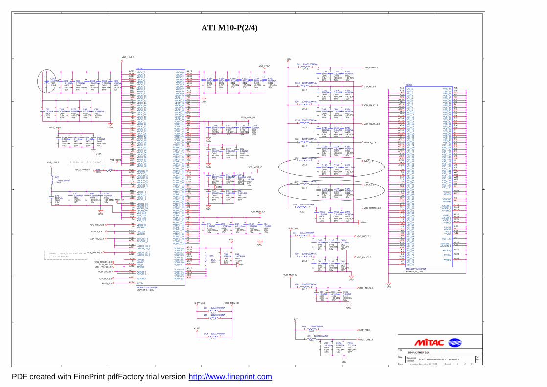
5
5
4
4
3
3
2
2
1
1
D D
C C
B B
A A
CONNECT LVDDR_25 TO 1.8V FOR M9, TO 2.5V FOR M10
1.8V for M9 , 1.5V for M10
ATI M10-P(2/4)
PCB 316680900001/ASSY 411680900011 R01
8050 MOTHER B/D
C
8 34Monday, December 29, 2003
Title
Size DocumentNumber
Rev
Date: Sheet of
GND
VDD_CORE
GND
+3V
GND
AVDD_1.8
GND
GND
VGA_1.2/1.0
VGA_1.2/1.0
VDD_DAC2.5
VDD_MEM_IO
A2VDDQ_1.8
AVDD_1.8VDD_CORE
VDD_PLL1.8
GND
VDD_MEM_IO
AGP_VDDQ+1.8V
VDD_PLL1.8
VDD_MEMPLL1.8
VDD_MEM_IO
VDD_PNLIO1.8
GND
VDD_MCLK2.5
AGP_VDDQ
VDD_PNLPLL1.8
GND
VDD_MEM_IOGND
+1.5V
VDD_DAC2.5
GND
VDD_PNLIO1.8
VDD_CORE1.5
VDD_PNLPLL1.8
+1.8V
GND
VDD_MEMPLL1.8
VDDDI_1.8
VDD_PNLIO2.5
VDD_PNLIO2.5
GND
A2VDDQ_1.8
VDD_CORE1.5
GND
GND
VDD_MEM_IO
VDD_CORE1.8
VDDDI_1.8
+2.5V_M10
+2.5V_M10
VDD_MCLK2.5
GND
VDD_MEM_IO
L35 120Z/100M/NA
2012
1 2
C1350.1U/NA0402
50V+80-20%
12
L705 120Z/100M/NA
20121 2
C1320.01U/NA0402
50V+80-20%
12
C1360.1U/NA0402
50V+80-20%
12
C1250.1U/NA0402
50V+80-20%
12
C910.01U/NA0402
50V+80-20%
12
C540.1U/NA0402
50V+80-20%
12
C76210U/NA
6.3V0805
10%
12
C800.1U/NA0402
50V+80-20%
12
C1110.1U/NA0402
50V+80-20%
12
C7690.1U/NA0402
50V+80-20%
12
C1520.1U/NA0402
50V+80-20%
12
C1070.1U/NA0402
50V+80-20%
12
C7370.1U/NA0402
50V+80-20%
12
C12710U/NA
6.3V0805
10%
12
C810.1U/NA0402
50V+80-20%
12
C1081000P/NA0402
50V+/-20%
12
C770.01U/NA0402
50V+80-20%
12
C960.01U/NA0402
50V+80-20%
12
R55
0/NA0805
12
C880.1U/NA0402
50V+80-20%
12
C741000P/NA0402
50V+/-20%
12
U710D
MOBILITY-M10-P/NABGA644_64_1MM
AC13AC15AC17AD13AD15M12M13M14M17M18M19N12N13N14N17N18N19P12P13P14P17P18P19U12U13U14U17U18U19V12V13V14V17V18V19
W12W13W14W17W18W19
W30Y27
AA23AA24AB30AC23AC27AE30AF27J30M23M24N30P23P27T23T24T30U27V23V24
A15A21A28A3A9AA1AA4AA7AA8AD4B1B30D11D14D17D20D23D26D5D8E27F4G10G13G15G19G22G27G7H10H13H15H17H19H22J1J23J24J4J7J8L27L8M4N7N8R1R4T7T8V4V7V8
AC11AC20
H11H20L23P8
Y23Y8
M15R19T12
W16
F18N6
AE24AE22
AF13AF14
AE15AF21
AE17AE20
AJ20A7
AK28AK12
AG21AH21
AF22
AH24
AC19AC21AC22AC8AD19AD21AD22AD7
AC9AD10AD9AG7
AC10
D13D19
N4T4
AB4D10D25
E4
VDDC_0VDDC_1VDDC_2VDDC_3VDDC_4VDDC_5VDDC_6VDDC_7VDDC_8VDDC_9VDDC_10VDDC_11VDDC_12VDDC_13VDDC_14VDDC_15VDDC_16VDDC_17VDDC_18VDDC_19VDDC_20VDDC_21VDDC_22VDDC_23VDDC_24VDDC_25VDDC_26VDDC_27VDDC_28VDDC_29VDDC_30VDDC_31VDDC_32VDDC_33VDDC_34VDDC_35VDDC_36VDDC_37VDDC_38VDDC_39VDDC_40
VDDP_19VDDP_20
VDDP_0VDDP_1VDDP_2VDDP_3VDDP_4VDDP_5VDDP_6VDDP_7VDDP_8VDDP_9
VDDP_10VDDP_11VDDP_12VDDP_13VDDP_14VDDP_15VDDP_16VDDP_17VDDP_18
VDDR1_0VDDR1_1VDDR1_2VDDR1_3VDDR1_4VDDR1_5VDDR1_6VDDR1_7VDDR1_8VDDR1_9
VDDR1_10VDDR1_11VDDR1_12VDDR1_13VDDR1_14VDDR1_15VDDR1_16VDDR1_17VDDR1_18VDDR1_19VDDR1_20VDDR1_21VDDR1_22VDDR1_23VDDR1_24VDDR1_25VDDR1_26VDDR1_27VDDR1_28VDDR1_29VDDR1_30VDDR1_31VDDR1_32VDDR1_33VDDR1_34VDDR1_35VDDR1_36VDDR1_37VDDR1_38VDDR1_39VDDR1_40VDDR1_41VDDR1_42VDDR1_43VDDR1_44VDDR1_45VDDR1_46VDDR1_47VDDR1_48VDDR1_49VDDR1_50VDDR1_51VDDR1_52
VDDC15_0VDDC15_1VDDC15_2VDDC15_3VDDC15_4VDDC15_5VDDC15_6VDDC15_7
VDDCI_0VDDCI_1VDDCI_2VDDCI_3
VDDRH0VDDRH1
VDD1DIVDD2DI
TXVDDR_0TXVDDR_1
LVDDR_18_0LVDDR_18_1
LVDDR_25_0LVDDR_25_1
LPVDDMPVDDPVDDTPVDD
A2VDD_0A2VDD_1
A2VDDQ
AVDD
VDDR3_0VDDR3_1VDDR3_2VDDR3_3VDDR3_4VDDR3_5VDDR3_6VDDR3_7
VDDR4_1VDDR4_2VDDR4_3VDDR4_4
VDDR4_0
VDDR1_53VDDR1_54VDDR1_55VDDR1_56VSS_119VSS_120VSS_121VSS_122
C950.01U/NA0402
50V+80-20%
12
L710 120Z/100M/NA
2012
1 2
C7670.1U/NA0402
50V+80-20%
12
C75810U/NA
6.3V0805
10%
12
C900.1U/NA0402
50V+80-20%
12
U710E
MOBILITY-M10-P/NABGA644_64_1MM
A10A16A2
A22A29
AA30AB1
AB23AB24AB27AB7AB8
AC12AC14AC16AC18AC4
AD12AD16AD18AD25AD30AE27AG11AG15AG18AG22AG27AG5AG9AJ1
AJ30AK2
AK29C1
C28C3
C30D12D15D18D21D24D27D4D6D9
F27G12G16G18G21G24G9
H12H14H16H18H21H23H27H4H8H9K1
K23K24K27K30K7
AE23AE21
F19M6
AG13AG14AH12
AH23
AD24
AF23
AH22AJ21
AJ19
AE16AE19AF15AF20
A6AJ28AJ12
P15P16P4R12R13R14R15R16R17R18R23
K8
U23
L4M16M30M7M8
R24R30R7R8T1T13T14T15T16T17T18T19T27U15U16U4U8V15V16V30W15W23W24W27W7W8Y4
N15N16N23N24N27
VSS_0VSS_1VSS_2VSS_3VSS_4VSS_5VSS_6VSS_7VSS_8VSS_9VSS_10VSS_11VSS_12VSS_13VSS_14VSS_15VSS_16VSS_17VSS_18VSS_19VSS_20VSS_21VSS_22VSS_23VSS_24VSS_25VSS_26VSS_27VSS_28VSS_29VSS_30VSS_31VSS_32VSS_33VSS_34VSS_35VSS_36VSS_37VSS_38VSS_39VSS_40VSS_41VSS_42VSS_43VSS_44VSS_45VSS_46VSS_47VSS_48VSS_49VSS_50VSS_51VSS_52VSS_53VSS_54VSS_55VSS_56VSS_57VSS_58VSS_59VSS_60VSS_61VSS_62VSS_63VSS_64VSS_65VSS_66VSS_67VSS_68VSS_69
VSS1DIVSS2DI
VSSRH0VSSRH1
TXVSSR_0TXVSSR_1TXVSSR_2
AVSSN
AVSSQ
A2VSSQ
A2VSSN_0A2VSSN_1
LPVSS
LVSSR_0LVSSR_1LVSSR_2LVSSR_3
MPVSSPVSS
TPVSS
VSS_81VSS_82VSS_83VSS_84VSS_85VSS_86VSS_87VSS_88VSS_89VSS_90VSS_91
VSS_70
VSS_123
VSS_71VSS_72VSS_73VSS_74VSS_75
VSS_92VSS_93VSS_94VSS_95VSS_96VSS_97VSS_98VSS_99
VSS_100VSS_101VSS_102VSS_103VSS_104VSS_105VSS_106VSS_107VSS_108VSS_109VSS_110VSS_111VSS_112VSS_113VSS_114VSS_115VSS_116VSS_117VSS_118
VSS_76VSS_77VSS_78VSS_79VSS_80
C1060.01U/NA0402
50V+80-20%
12
C1390.1U/NA0402
50V+80-20%
12
C8410U/NA
6.3V0805
10%
12
L26 120Z/100M/NA
20121 2
C1050.1U/NA0402
50V+80-20%
12
L31 120Z/100M/NA
20121 2
C9810U/NA
6.3V0805
10%
12
C1530.1U/NA0402
50V+80-20%
12
C7640.1U/NA0402
50V+80-20%
12
C860.1U/NA0402
50V+80-20%
12
L29 120Z/100M/NA
2012
1 2
C1240.1U/NA0402
50V+80-20%
12
C13810U/NA
6.3V0805
10%
12
C8910U/NA
6.3V0805
10%
12
C761000P/NA0402
50V+/-20%
12
C1130.1U/NA0402
50V+80-20%
12
C850.01U/NA0402
50V+80-20%
12
C1090.1U/NA0402
50V+80-20%
12
C1170.01U/NA0402
50V+80-20%
12
C7910U/NA
6.3V0805
10%
12
C1190.1U/NA0402
50V+80-20%
12
C660.01U/NA0402
50V+80-20%
12
C441000P/NA0402
50V+/-20%
12
C11410U/NA
6.3V0805
10%
12
R94 0/NA0805
1 2
L28
120Z/100M/NA2012
12
C750.1U/NA0402
50V+80-20%
12
C7810U/NA
6.3V0805
10%
12
C7630.1U/NA0402
50V+80-20%
12
C991000P/NA0402
50V+/-20%
12
C580.01U/NA0402
50V+80-20%
12
C1370.01U/NA0402
50V+80-20%
12
C1160.1U/NA0402
50V+80-20%
12
C73910U/NA
6.3V0805
10%
12
C1011000P/NA0402
50V+/-20%
12
C11210U/NA
6.3V0805
10%
12
+ C743150U/NA73432.5V
12
C1300.1U/NA0402
50V+80-20%
12
C1180.1U/NA0402
50V+80-20%
12
C14110U/NA
6.3V0805
10%
12
C1001000P/NA0402
50V+/-20%
12
L712 120Z/100M/NA
2012
1 2
C7470.1U/NA0402
50V+80-20%
12
L32 120Z/100M/NA
2012
1 2
C7460.1U/NA0402
50V+80-20%
12
C600.01U/NA0402
50V+80-20%
12
C1340.1U/NA0402
50V+80-20%
12
L709 120Z/100M/NA
2012
1 2
C1030.1U/NA0402
50V+80-20%
12
L27 120Z/100M/NA
20121 2
C5510U/NA
6.3V0805
10%
12
C12110U/NA
6.3V0805
10%
12
C1150.1U/NA0402
50V+80-20%
12
L24 120Z/100M/NA
20121 2
C971000P/NA0402
50V+/-20%
12
C9210U/NA
6.3V0805
10%
12
C73610U/NA
6.3V0805
10%
12
C8210U/NA
6.3V0805
10%
12
L34 120Z/100M/NA
2012
1 2
L39 120Z/100M/NA
20121 2
C7380.1U/NA0402
50V+80-20%
12
L30 120Z/100M/NA
2012
1 2
C1471000P/NA0402
50V+/-20%
12
C1290.1U/NA0402
50V+80-20%
12
C16410U/NA
6.3V0805
10%
12
C871000P/NA0402
50V+/-20%
12
L33 120Z/100M/NA
20121 2
C1020.1U/NA0402
50V+80-20%
12
C16710U/NA
6.3V0805
10%
12
C830.1U/NA0402
50V+80-20%
12
C1400.1U/NA0402
50V+80-20%
12
C5010U/NA
6.3V0805
10%
12
L40 120Z/100M/NA
20121 2
PDF created with FinePrint pdfFactory trial version http://www.fineprint.com
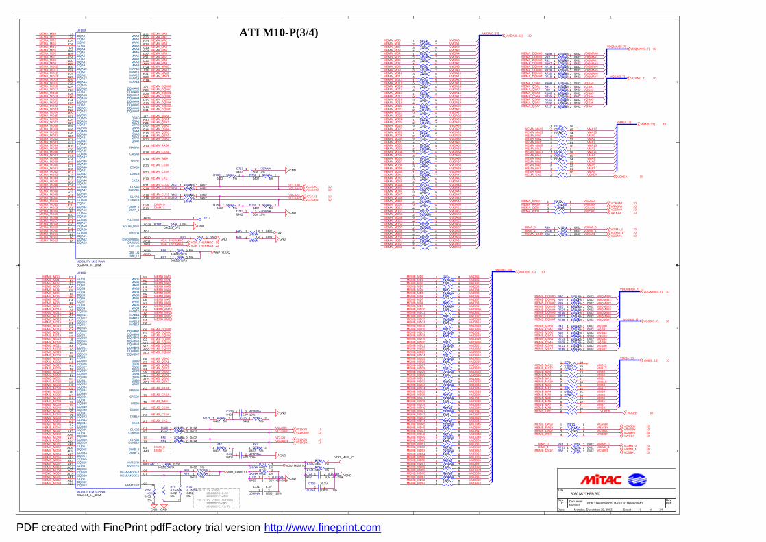
5
5
4
4
3
3
2
2
1
1
D D
C C
B B
A A
MEMVMODE=1.8VMEMVMODE1=GND
MEMVMODE1=1.8V
FOR 2.5V VDDR1
MEMVMODE=GNDFOR 1.8V VDDR1(ELPIDA)
ATI M10-P(3/4)
PCB 316680900001/ASSY 411680900011 R01
8050 MOTHER B/D
C
9 34Monday, December 29, 2003
Title
Size DocumentNumber
Rev
Date: Sheet of
VMDB[0..63]
VDQMA#[0..7]
VQSA[0..7]
VQSB[0..7]
VDQMB#[0..7]
VMDA[0..63]
MEMA_MD2MEMA_MD3MEMA_MD4MEMA_MD5
MEMA_MD8
MEMA_MD10
MEMA_MD6
MEMA_MD9
MEMA_MD7
MEMA_MD11
MEMA_MD14
MEMA_MD16
MEMA_MD12
MEMA_MD15
MEMA_MD13
MEMA_MD17
MEMA_MD20
MEMA_MD22
MEMA_MD18
MEMA_MD21
MEMA_MD19
MEMA_MD23
MEMA_MD26
MEMA_MD28
MEMA_MD24
MEMA_MD27
MEMA_MD25
MEMA_MD29
MEMA_MD32
MEMA_MD34
MEMA_MD30
MEMA_MD33
MEMA_MD31
MEMA_MD35
MEMA_MD38
MEMA_MD40
MEMA_MD36
MEMA_MD39
MEMA_MD37
MEMA_MD41
MEMA_MD44
MEMA_MD46
MEMA_MD42
MEMA_MD45
MEMA_MD43
MEMA_MD47
MEMA_MD54
MEMA_MD49
MEMA_MD52
MEMA_MD55
MEMA_MD59
MEMA_MD53
MEMA_MD58
MEMA_MD50
MEMA_MD57
MEMA_MD48
MEMA_MD56
MEMA_MD51
MEMA_MD61
MEMA_MD63MEMA_MD62
MEMA_MD60
MEMA_MA0MEMA_MA1MEMA_MA2MEMA_MA3MEMA_MA4
MEMA_MA9
MEMA_MA5MEMA_MA6MEMA_MA7MEMA_MA8
MEMA_MA10MEMA_MA11MEMA_MA12MEMA_MA13
MEMA_DQM#4
MEMA_DQM#0MEMA_DQM#1MEMA_DQM#2MEMA_DQM#3
MEMA_DQM#5
MEMA_DQM#7MEMA_DQM#6
MEMA_QSA2
MEMA_QSA5MEMA_QSA4MEMA_QSA3
MEMA_QSA7MEMA_QSA6
MEMA_QSA1MEMA_QSA0
MEMA_RAS#
MEMA_CAS#
MEMA_WE#
MEMA_CS0#
MEMA_CS1#
MEMA_CKE
MEMA_MD22
MEMA_MD12
MEMA_MD7
MEMA_MD35
MEMA_MD15
MEMA_MD10
MEMA_MD42
MEMA_MD29
MEMA_MD48
MEMA_MD4
MEMA_MD21
MEMA_MD31
MEMA_MD8
MEMA_MD34
MEMA_MD13
MEMA_MD25
MEMA_MD19
MEMA_MD61
MEMA_MD30
MEMA_MD57
MEMA_MD51
MEMA_MD59
MEMA_MD6
MEMA_MD37
MEMA_MD52
MEMA_MD32
MEMA_MD53
MEMA_MD16
MEMA_MD11
MEMA_MD58
MEMA_MD27
MEMA_MD50
MEMA_MD40
MEMA_MD9
MEMA_MD54
MEMA_MD63
MEMA_MD0
MEMA_MD55
MEMA_MD33
MEMA_MD43
MEMA_MD20
MEMA_MD47
MEMA_MD41
MEMA_MD26
MEMA_MD46
MEMA_MD38
MEMA_MD49
MEMA_MD23
MEMA_MD17
MEMA_MD24
MEMA_MD45
MEMA_MD18
MEMA_MD60
MEMA_MD1
MEMA_MD36
MEMA_MD62
MEMA_MD14
MEMA_MD5
MEMA_MD28
MEMA_MD44
MEMA_MD56
MEMA_MD39
MEMA_CLK0MEMA_CLK0#
MEMA_CLK1MEMA_CLK1#
VCLKA0VCLKA#0
VCLKA1VCLKA#1
VCLKB0
VCLKB1VCLKB#1
VCLKB#0
DIMA_0DIMA_1
MEMA_MD0MEMA_MD1
MEMA_QSA4
MEMA_DQM#7
MEMA_DQM#0
MEMA_DQM#6
MEMA_DQM#2
MEMA_QSA7
MEMA_DQM#4
MEMA_DQM#1
MEMA_QSA2
MEMA_QSA0
MEMA_DQM#5
MEMA_QSA5
MEMA_DQM#3
MEMA_QSA1
MEMA_QSA3
MEMA_RAS#MEMA_CAS#
MEMA_WE#
VDQMA#6
VDQMA#3VDQMA#2
VDQMA#5VDQMA#4
VDQMA#1
VDQMA#7
VQSA3
VQSA7
VQSA5
VQSA0
VQSA4
VQSA1
VMDB49
VMDB31
VMDB39
VMDB50
VMDB63
VMDB52
VMDB20
VMDB22
VMDB29
VMDB8
VMDB5
VMDB28
VMDB32
VMDB37
VMDB44
VMDB30
VMDB55
VMDB1
VMDB25
VMDB54
VMDB60
VMDB45
VMDB53
VMDB7
VMDB42
VMDB56
VMDB24
VMDB6
VMDB18VMDB17
VDQMB#6VDQMB#7
VDQMB#4VDQMB#3
VDQMB#5
VDQMB#1
VQSB3
VQSB7
VQSB1
VQSB6
VQSB0
VQSB2
VDQMA#0
VQSA2
VQSA6MEMA_QSA6
MEMB_QSA0
MEMB_DQM#5
MEMB_QSA1
MEMB_QSA5
MEMB_DQM#7
MEMB_QSA6
MEMB_QSA4
MEMB_QSA7
MEMB_QSA2
MEMB_DQM#4
MEMB_DQM#1MEMB_DQM#0
MEMB_DQM#6
MEMB_QSA3
MEMB_DQM#3
VDQMB#0
VDQMB#2
VQSB4VQSB5
MEMB_DQM#2
VGA_THERMDCVGA_THERMDA
VMDA60
VMDA34
VMDA27
VMDA20
VMDA49
VMDA16
VMDA4
VMDA28
VMDA10
VMDA14
VMDA44
VMDA47
VMDA58
VMDA21
VMDA7
VMDA12
VMDA18
VMDA50
VMDA13
VMDA39
VMDA53
VMDA3
VMDA32
VMDA63
VMDA23
VMDA31
VMDA1
VMDA9
VMDA19
VMDA15
VMDA6
VMDA11
VMDA17
VMDA8
VMDA5
VMDA26VMDA25
VMDA29
VMDA35
VMDA22
VMDA33
VMDA30
VMDA24
VMDA42VMDA41
VMDA36
VMDA45
VMDA48
VMDA51
VMDA38
VMDA43
VMDA46
VMDA40
VMDA37
VMDA57
VMDA52
VMDA61
VMDA55VMDA54
VMDA59
VMDA62
VMDA56
MEMB_MD14
MEMB_MD43
MEMB_MD63
MEMB_MD16
MEMB_MD40
MEMB_MD12
MEMB_MD59
MEMB_MD19
MEMB_MD24
MEMB_MD18
MEMB_MD50
MEMB_MD22
MEMB_MD48
MEMB_MD7
MEMB_MD26
MEMB_MD20
MEMB_MD34
MEMB_MD38
MEMB_MD55
MEMB_MD31
MEMB_MD10
MEMB_MD2
MEMB_MD51
MEMB_MD11
MEMB_MD29
MEMB_MD37
MEMB_MD5
MEMB_MD52MEMB_MD53
MEMB_MD61
MEMB_MD15
MEMB_MD42
MEMB_MD39
MEMB_MD46
MEMB_MD13
MEMB_MD6
MEMB_MD35
MEMB_MD49
MEMB_MD27
MEMB_MD41
MEMB_MD8
MEMB_MD28
MEMB_MD54
MEMB_MD57
MEMB_MD36
MEMB_MD0
MEMB_MD32
MEMB_MD56
MEMB_MD9
MEMB_MD60
MEMB_MD25
MEMB_MD23
MEMB_MD47
MEMB_MD4
MEMB_MD1
MEMB_MD33
MEMB_MD62
MEMB_MD17
MEMB_MD45
MEMB_MD21
MEMB_MD30
MEMB_MD44
MEMB_MD3
MEMB_MD58
VMDB0
VMDB9
VMDB12
VMDB15
VMDB3
VMDB11
VMDB2
VMDB14VMDB13
VMDB10
VMDB4
VMDB21
VMDB16
VMDB19
VMDB27
VMDB23
VMDB26
VMDB40
VMDB38
VMDB41
VMDB47
VMDB35
VMDB43
VMDB34
VMDB46
VMDB36
VMDB33
VMDB48
VMDB57
VMDB51
VMDB59
VMDB62VMDB61
VMDB58
DIMA_1DIMA_0 VDIMA_0
VDIMA_1
DIMB_0DIMB_1 VDIMB_1
VDIMB_0
MEMA_MD2MEMA_MD3
VMDA0
VMDA2
MEMA_CS1#
VCSB#1MEMB_CS1#
MEMB_MA13
MEMB_MA3
MEMB_MD48
MEMB_MD9
MEMB_MD51
MEMB_MD30
MEMB_MD0
MEMB_DQM#0
MEMB_MA11
MEMB_MD50
MEMB_MD39
MEMB_MD12
MEMB_MD4
MEMB_CS1#
MEMB_WE#
MEMB_DQM#3MEMB_DQM#2
MEMB_MD47
MEMB_MD44
MEMB_MD24MEMB_MD23
MEMB_QSA3
MEMB_MD14
MEMB_MD5
MEMB_MD2
DIMB_1
MEMB_CKE
MEMB_MD49
MEMB_MD45
MEMB_MD28
MEMB_MD26
MEMB_MD18
DIMB_0
MEMB_QSA5
MEMB_MD63
MEMB_MD22
MEMB_MD10
MEMB_QSA4
MEMB_MD56
MEMB_MD43
MEMB_MD34
MEMB_MD11
MEMB_MD8MEMB_MD7
MEMB_MD3
MEMB_MA5
MEMB_MD62
MEMB_MD40
MEMB_MD15
MEMB_QSA6
MEMB_QSA2
MEMB_MD57
MEMB_MD52
MEMB_MD25
MEMB_MD6
MEMB_CS0#
MEMB_DQM#5
MEMB_MD29
MEMB_QSA7
MEMB_DQM#7
MEMB_MA12
MEMB_MA9MEMB_MA8
MEMB_MD55
MEMB_MD53
MEMB_MD42MEMB_MD41
MEMB_MD32
MEMB_CAS#
MEMB_QSA0
MEMB_MD21
MEMB_MD13
MEMB_QSA1
MEMB_DQM#6
MEMB_MA7MEMB_MA6
MEMB_MD61
MEMB_MD59
MEMB_MD37MEMB_MD36
MEMB_MD33
MEMB_MD17
MEMB_RAS#
MEMB_MA10
MEMB_MD20MEMB_MD19
MEMB_DQM#4
MEMB_DQM#1
MEMB_MA0
MEMB_MD60
MEMB_MD54
MEMB_MD46
MEMB_MD38
MEMB_MD31
MEMB_MD27
MEMB_MD1
MEMB_MA4
MEMB_MA2
MEMB_MD58
MEMB_MD35
MEMB_MD16
MEMB_MA1
VCSA#1
MEMB_MA5MEMB_MA7
MEMB_MA4
MEMB_MA6MEMB_MA9
MEMB_MA11
MEMB_MA8VCKEBMEMB_CKE
MEMA_MA3
MEMA_MA0
MEMA_CS0#
MEMA_MA10MEMA_MA1MEMA_MA2
MEMA_MA13MEMA_MA12
VRASA#
VWEA#VCSA#0
VCASA#
VCASB#
VCSB#0MEMB_RAS# VRASB#
VWEB#
MEMB_CAS#
MEMB_CS0#MEMB_WE#
MEMB_MA10
MEMB_MA13
VMB[0..13]
VMB13
MEMB_MA1
VMB12
VMB4VMB11
MEMB_MA0
VMB9
VMB0
VMB10VMB3
VMB8
MEMB_MA12
VMB5VMB7
VMB6
MEMB_MA3
MEMB_MA2 VMB2VMB1
VCKEA
VMA0
MEMA_MA11
VMA13
VMA5
MEMA_CKEMEMA_MA8
VMA2
MEMA_MA5
VMA[0..13]
VMA9
VMA1VMA10
MEMA_MA9
VMA12
MEMA_MA6
VMA3
VMA6
VMA7MEMA_MA7
MEMA_MA4
VMA8
VMA4VMA11
VCLKA0 10VCLKA#0 10
VCLKA1 10VCLKA#1 10
VCLKB1 10
VCLKB#0 10
VCLKB#1 10
VCLKB0 10
VMDB[0..63] 10
VMDA[0..63] 10
VDQMA#[0..7] 10
VQSA[0..7] 10
VDQMB#[0..7] 10
VQSB[0..7] 10
VDIMA_0 10VDIMA_1 10
VDIMB_1 10VDIMB_0 10
VCSB#1 10
VGA_THERMDA 22VGA_THERMDC 22
VCSA#1 10
VMB[0..13] 10
VCSB#0 10
VCKEB 10
VRASB# 10
VWEB# 10
VCASB# 10
VCSA#0 10
VCKEA 10
VMA[0..13] 10
VRASA# 10
VWEA# 10
VCASA# 10
AGP_VDDQ
GND
GND
GND
+3V
GND GND
GND
GND
VDD_CORE1.8
VDD_MEM_IO
GND
GND
GND
VDD_MEM_IO
GND
R7411K/NA 0402 1%
1 2
U710C
MOBILITY-M10-P/NABGA644_64_1MM
D7F7E7G6G5F5E5C4B5C5A4B4C2D3D1D2G4H6H5J6K5K4L6L5G2F3H2E2F2J3F1H3U6U5U3V6
W5W4Y6Y5U2V2V1V3
W3Y2Y3
AA2AA6AA5AB6AB5AD6AD5AE5AE4AB2AB3AC2AC3AD3AE1AE2AE3
N5M1M3L3L2M2M5P6N3K2K3J2P5P3
E6B2J5G3W6W2AC6AD2
F6B3K6G1V5W1AC5AD1
R2
T5
T6
R5
R6
R3
N1N2
T2T3
C6C7
C8
B7
P2
B8
E3AA3
DQB0DQB1DQB2DQB3DQB4DQB5DQB6DQB7DQB8DQB9DQB10DQB11DQB12DQB13DQB14DQB15DQB16DQB17DQB18DQB19DQB20DQB21DQB22DQB23DQB24DQB25DQB26DQB27DQB28DQB29DQB30DQB31DQB32DQB33DQB34DQB35DQB36DQB37DQB38DQB39DQB40DQB41DQB42DQB43DQB44DQB45DQB46DQB47DQB48DQB49DQB50DQB51DQB52DQB53DQB54DQB55DQB56DQB57DQB58DQB59DQB60DQB61DQB62DQB63
MAB0MAB1MAB2MAB3MAB4MAB5MAB6MAB7MAB8MAB9
MAB10MAB11MAB12MAB13
DQMB#0DQMB#1DQMB#2DQMB#3DQMB#4DQMB#5DQMB#6DQMB#7
QSB0QSB1QSB2QSB3QSB4QSB5QSB6QSB7
RASB#
CASB#
WEB#
CSB0#
CSB1#
CKEB
CLKB0CLKB0#
CLKB1CLKB1#
MEMVMODE0MEMVMODE1
MEMTEST
MVREFD
MAB14
MVREFS
DIMB_0DIMB_1
RP71124*4/NA1206
1234
8765
RP70524*4/NA1206
1234
8765
R4256/NA
0402 5%1 2
C729 470P/NA0402 50V 10%
1 2
R51 10/NA 04025%1 2
R74 4.7K/NA0402 5%
1 2
R75047/NA
04025%
12
R109 24/NA 04025%1 2
RP1824*4/NA1206
1234
8765
R758 56/NA0402 5%
1 2
RP1224*4/NA1206
1234
8765
RP324*4/NA1206
1234
8765
RP924*4/NA1206
1234
8765
RP70824*4/NA1206
1234
8765
RP2324*4/NA1206
1234
8765
RP71024*4/NA1206
1234
8765
R35 24/NA 04025%1 2
C751 470P/NA0402 50V 10%
1 2
R98 0/NA 5%0402G_DFS1 2
R756 56/NA0402 5%
1 2
RP424*4/NA1206
1234
8765
R757 10/NA 04025%1 2
R29 24/NA 04025%1 2
RP1724*4/NA1206
1234
8765
RP1124*4/NA1206
1234
8765
R727 10/NA 04025%1 2
R731 24/NA 04025%1 2
R716 24/NA 04025%1 2
R41 24/NA 04025%1 2
R761 10/NA 04025%1 2
R69 4.7K/NA0402 5%
1 2
R723 24/NA 04025%1 2
RP2124*4/NA1206
1234
8765
R725 56/NA0402 5%
1 2
RP71224*4/NA1206
1234
8765
R787 0/NA 5%0402G_DFS1 2
RP70424*4/NA1206
1234
8765
R97 0/NA 5%0402G_DFS1 2
R759 10/NA 04025%1 2
R718 24/NA 04025%1 2
RP70124*4/NA1206
1234
8765
RP2024*4/NA1206
1234
8765
R746 0/NA 04021 2
R75510/NA
04025%1 2
R722 24/NA 04025%1 2
RP100*4/NA1206
1234
8765
RP70724*4/NA1206
1234
8765
C730
10U/NA
6.3V
0805 10%1 2
R50 10/NA 04025%1 2
R726 56/NA0402 5%1 2
R721 24/NA 04025%1 2
R106 24/NA 04025%1 2
R7361K/NA 0402 1%
1 2
R724 24/NA 04025%1 2
R39 24/NA 04025%1 2
RP60*8/NARPX8
12345678 9
10111213141516
R441K/NA
04021%1 2
RP71324*4/NA1206
1234
8765
C742 470P/NA0402 50V 10%
1 2
R747 0/NA 5%0402G_DFS1 2
R711 0/NA 04021 2
TP171
RP71724*4/NA1206
1234
8765
RP724*4/NA1206
1234
8765
RP1324*4/NA1206
1234
8765
RP524*4/NA1206
1234
8765
R36 0/NA 04021 2
R81 0/NA 04021 2
R709 24/NA 04025%1 2
R729 24/NA 04025%1 2R719 24/NA 04025%1 2
C41 470P/NA0402 50V 10%
1 2
RP80*8/NARPX8
12345678 9
10111213141516
R93 24/NA 04025%1 2
R754.7K/NA04025%
12
RP70324*4/NA1206
1234
8765
R451K/NA
04021%1 2
RP140*8/NARPX8
12345678 9
10111213141516
R30 24/NA 04025%1 2
R717 24/NA 04025%1 2
R33 24/NA 04025%1 2
C735 0.1U/NA0402 50V +80-20%
1 2
R4356/NA
0402 5%1 2
R92 24/NA 04025%1 2
R31 0/NA 04021 2
RP2424*4/NA1206
1234
8765
R80 0/NA 04021 2
RP70224*4/NA1206
1234
8765
R91 24/NA 04025%1 2
C732 0.1U/NA0402 50V +80-20%
1 2
R89 0/NA 04021 2
R40 24/NA 04025%1 2
RP2224*4/NA1206
1234
8765
RP70624*4/NA1206
1234
8765
RP71624*4/NA1206
1234
8765
U710B
MOBILITY-M10-P/NABGA644_64_1MM
L25L26K25K26J26H25H26G26G30D29D28E28E29G29G28F28G25F26E26F25E24F23E23D22B29C29C25C27B28B25C26B26F17E17D16F16E15F14E14F13C17B18B17B15C13B14C14C16A13A12C12B12C10C9B9
B10E13E12E10F12F11E9F9F8
E22B22B23B24C23C22F22F21C21A24C24A25E21B20
J25F29E25A27F15C15C11E11
J27F30F24B27E16B16B11F10
A19
E18
E19
E20
F20
B19
B21C20
C18A18
AG4
AE10AE11AF11
AB26AB25
AG29
AE25
C19
D30B13
DQA0DQA1DQA2DQA3DQA4DQA5DQA6DQA7DQA8DQA9DQA10DQA11DQA12DQA13DQA14DQA15DQA16DQA17DQA18DQA19DQA20DQA21DQA22DQA23DQA24DQA25DQA26DQA27DQA28DQA29DQA30DQA31DQA32DQA33DQA34DQA35DQA36DQA37DQA38DQA39DQA40DQA41DQA42DQA43DQA44DQA45DQA46DQA47DQA48DQA49DQA50DQA51DQA52DQA53DQA54DQA55DQA56DQA57DQA58DQA59DQA60DQA61DQA62DQA63
MAA0MAA1MAA2MAA3MAA4MAA5MAA6MAA7MAA8MAA9
MAA10MAA11MAA12MAA13
DQMA#0DQMA#1DQMA#2DQMA#3DQMA#4DQMA#5DQMA#6DQMA#7
QSA0QSA1QSA2QSA3QSA4QSA5QSA6QSA7
RASA#
CASA#
WEA#
CSA0#
CSA1#
CKEA
CLKA0CLKA0#
CLKA1CLKA1#
VREFG
DVOVMODEDMINUS
DPLUS
DBI_LODBI_HI
RSTB_MSK
PLLTEST
MAA14
DIMA_0DIMA_1
R107 24/NA 04025%1 2
R730 24/NA 04025%1 2
R732 24/NA 04025%1 2
R7451K/NA 0402 1%
1 2
R710 24/NA 04025%1 2
R38 24/NA 04025%1 2
RP160*4/NA1206
1234
8765
R754 56/NA0402 5%
1 2
RP150*8/NARPX8
12345678 9
10111213141516
R108 24/NA 04025%1 2
R728 10/NA 04025%1 2
R715 24/NA 04025%1 2
R760 56/NA0402 5%
1 2
R704.7K/NA04025%
12
C731
10U/NA
6.3V
0805 10%1 2
R7401K/NA 0402 1%
1 2
R90 24/NA 04025%1 2
RP70924*4/NA1206
1234
8765
R720 24/NA 04025%1 2RP1924*4/NA1206
1234
8765
RP71424*4/NA1206
1234
8765
PDF created with FinePrint pdfFactory trial version http://www.fineprint.com
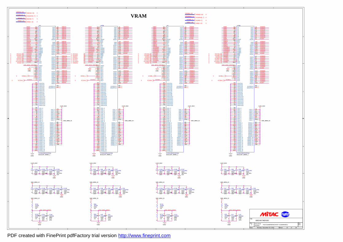
5
5
4
4
3
3
2
2
1
1
D D
C C
B B
A A
VRAM
PCB 316680900001/ASSY 411680900011 R01
8050 MOTHER B/D
C
10 34Monday, December 29, 2003
Title
Size DocumentNumber
Rev
Date: Sheet of
VQSB[0..7]VMA[0..13]
VMB[0..13]
VQSA[0..7]
VDQMA#[0..7]
VMDA[0..63]
VDQMB#[0..7]
VMDB[0..63]
VDQMA#0
VMDA30
VMA1
VQSA1
VMDA19
VMDA31
VMA3
VMDA7
VWEA#
VCSA#1
VMA13
VMA4
VMA6
VCASA#
VMA2
VMDA15
VMDA11
VDQMA#3
VMDA28
VMDA5
VMDA16
VMDA21
VMDA26
VMA10
VCLKA#0
VMA0
VQSA3
VMDA18
VMDA2
VMDA13
VMDA23VMDA22
VMA8
VMDA0
VCKEA
VMDA14
VCSA#0
VMA9
VMDA27
VQSA2
VRASA#
VMDA29
VMA11
VMDA25
VMDA12
VMDA24
VCLKA0
VMA12
VMDA17
VMA7
VMDA8
VMDA4
VMDA1
VDQMA#2
VMDA9
VMDA3
VMDA6
VDQMA#1
VMDA20
VMA5
VMDA10
VQSA0
VDD_MEM_IOREF
VDD_MEM_IOREF
VMDA47
VWEA#
VMDA52
VMDA36
VMDA46
VMDA51
VMDA38
VMDA56
VMA3
VMDA33
VMDA54
VMDA44
VMA1
VMDA35
VMA11
VMDA41
VMDA49
VMA0
VMDA45
VMDA62
VDQMA#5
VMDA59
VMA6
VMDA34
VMDA53
VMDA37
VMDA48
VMA9
VMDA61
VMDA32
VMDA40
VCLKA1
VMA10 VMDA42
VCKEA
VMDA58
VQSA6
VCSA#0
VDQMA#4
VCSA#1
VQSA7
VMA7
VMA2
VDQMA#6
VRASA#
VMA8
VMA13
VMDA55
VMDA60
VDQMA#7
VMDA50
VCASA#
VMA4
VMDA39VQSA4
VCLKA#1
VMDA63
VMDA43
VMA12
VMDA57
VQSA5
VMA5
VDD_MEM_IOREF
VDD_MEM_IOREF
VQSB2
VMB13
VMDB27
VMDB31
VMDB12
VMDB9
VDQMB#2
VMDB21
VCSB#0
VQSB3
VMB0
VQSB1
VMDB16
VMB10
VMB2
VDQMB#1VMDB14
VMB6
VQSB0VMB7
VCASB#
VMDB13
VMDB10
VMB4VMB5
VMDB23
VMDB25
VMDB15
VMDB11
VMB3
VCLKB0
VMB1
VDQMB#3
VMDB5
VCLKB#0
VMDB8
VMDB3VMDB4
VMDB30
VMB12VMB8
VMDB19VMDB18
VMDB1
VDQMB#0VMB11
VMDB17
VMDB0
VCKEB
VRASB#
VMDB29
VMB9
VMDB7
VWEB#
VMDB24
VCSB#1
VMDB26
VMDB22
VMDB28
VMDB20
VMDB2
VMDB6
VDD_MEM_IOREF
VDD_MEM_IOREF
VMDB49
VRASB#
VMDB51VCLKB1
VMB11
VMDB35
VMDB59
VMB7
VQSB7
VMB5
VMDB53
VMDB62
VMDB34
VMDB47
VMDB41
VMDB45
VMB1
VCASB#
VMB2
VWEB#
VDQMB#4
VMDB60
VMB6
VMDB46
VCKEB
VQSB6
VMDB40
VQSB5
VMDB39
VMDB42
VMB12
VMDB38
VMB8 VQSB4
VMDB52
VMDB61
VDQMB#7
VMB10
VMB0
VMB9
VCSB#1
VMDB55
VMDB33
VMDB50VCLKB#1
VMDB56
VMDB43
VMB3
VMDB44
VMDB36
VMDB54
VMDB63
VMB13
VMDB48
VDQMB#6
VMDB57
VMDB37
VCSB#0
VMDB58
VMDB32
VMB4
VDQMB#5
VDD_MEM_IOREF
VDD_MEM_IOREF
VDQMA#[0..7] 9
VWEA#9
VQSB[0..7] 9
VCLKA#09VCLKA09
VCSA#19
VMA[0..13] 9
VRASA#9
VQSA[0..7] 9
VCASA#9
VMDB[0..63] 9
VCKEA9
VMB[0..13] 9
VMDA[0..63] 9
VCSA#09
VDQMB#[0..7] 9
VDIMA_09
VCSA#19
VDIMA_19
VCASB#9
VCSB#19
VRASB#9
VWEB#9
VCKEB9
VCSB#09
VCLKB#09VCLKB09
VDIMB_09
VRASB#9
VCLKB19
VCKEB9VCLKB#19
VCASB#9
VCSB#19
VWEB#9VCSB#09
VDIMB_19
VRASA#9VCASA#9VWEA#9VCSA#09VCLKA19VCLKA#19VCKEA19
GND
VDD_MEM_IO
GND
+2.5V_M10
VDD_MEM_IO
GND
+2.5V_M10
GNDVDD_MEM_IO
GND
GND
VDD_MEM_IO
GND
+2.5V_M10
GND
VDD_MEM_IOGND
+2.5V_M10
GND
VDD_MEM_IO
GND
GND
VDD_MEM_IO
+2.5V_M10
VDD_MEM_IO
GND
GND
GNDVDD_MEM_IO
+2.5V_M10
GND
GND
VDD_MEM_IO
+2.5V_M10
VDD_MEM_IO
VDD_MEM_IO
+2.5V_M10
GND
GND
GND
C7410.1U/NA0402
16V10%
12
C7540.1U/NA0402
16V10%
12
R7131K/NA04021%
12
C3710U/NA
6.3V0805
10%
12
C7211U/NA0402
10V+80-20%
12
C270.1U/NA0402
16V10%
12
R321K/NA04021%
12
R7121K/NA04021%
12
C281U/NA0402
10V+80-20%
12
C7531U/NA0402
10V+80-20%
12
C7440.1U/NA0402
16V10%
12
C621U/NA0402
10V+80-20%
12
C7490.01U/NA0402
50V+80-20%
12
R7511K/NA04021%
12
C72210U/NA
6.3V0805
10%
12
U3
HY5DU2832222F/NABGA144F_08MM_1
M12
M4M5L5
M6M7L8
M8M9
M10M3L4L7
A2G11G2
A11L1K1K2M1L10
M11
L6
M2B3
B10G3
G10K11K12
K3
L2L3
G7G8H5
J3
H6
A1
B11
A6B5A5A4B1C2C1D1
J12J11H12H11F12F11E12E11
E2E1F2F1H2H1J1J2
D12C12C11B12A9A8B8A7
C6C7D3D10
K6K7K10
B2B4B6B7B9
D2D11E3E10F3F10H3H10
J5D9D7D6
K5
L11
H7H8G5G6E5E6E7E8F5F6F7F8
J6J7J8K4K9D4C8C9
C10D5D8E4E9F4F9G4G9H4H9J4J9
J10
G12
G1
A12
A3C3C4C5
A10
L12
K8L9
VREF
A0A1A2A3A4A5A6A7A8/APBA0BA1A9
DQM0DQM1DQM2DQM3RASCASWECSCK
CKE
A11
NC1NC2NC3NC4NC5NC6NC7
VDD_4
NC8NC9
VSS/TH1VSS/TH2VSS/TH3
VDDQ_14
VSS/TH4
DQS0
VDDQ_5
DQ0DQ1DQ2DQ3DQ4DQ5DQ6DQ7
DQ8DQ9
DQ10DQ11DQ12DQ13DQ14DQ15
DQ16DQ17DQ18DQ19DQ20DQ21DQ22DQ23
DQ24DQ25DQ26DQ27DQ28DQ29DQ30DQ31
VDD_0VDD_1VDD_2VDD_3
VDD_5VDD_6VDD_7
VDDQ_0VDDQ_1VDDQ_2VDDQ_3VDDQ_4
VDDQ_6VDDQ_7VDDQ_8VDDQ_9
VDDQ_10VDDQ_11VDDQ_12VDDQ_13
VSS_3VSS_2VSS_1VSS_0
A10
CK#
VSS/TH5VSS/TH6VSS/TH7VSS/TH8VSS/TH9VSS/TH10VSS/TH11VSS/TH12VSS/TH13VSS/TH14VSS/TH15VSS/TH16
VSS_4VSS_5VSS_6VSS_7VSS_8VSS_9VSSQ_0VSSQ_1VSSQ_2VSSQ_3VSSQ_4VSSQ_5VSSQ_6VSSQ_7VSSQ_8VSSQ_9VSSQ_10VSSQ_11VSSQ_12VSSQ_13VSSQ_14
VDDQ_15
DQS1
DQS2
DQS3
VSSQ_15VSSQ_16VSSQ_17VSSQ_18VSSQ_19
MCL
A12/RFU1BA2/RFU2
U709
HY5DU2832222F/NABGA144F_08MM_1
M12
M4M5L5
M6M7L8
M8M9
M10M3L4L7
A2G11G2
A11L1K1K2M1L10
M11
L6
M2B3
B10G3
G10K11K12
K3
L2L3
G7G8H5
J3
H6
A1
B11
A6B5A5A4B1C2C1D1
J12J11H12H11F12F11E12E11
E2E1F2F1H2H1J1J2
D12C12C11B12A9A8B8A7
C6C7D3D10
K6K7K10
B2B4B6B7B9
D2D11E3E10F3F10H3H10
J5D9D7D6
K5
L11
H7H8G5G6E5E6E7E8F5F6F7F8
J6J7J8K4K9D4C8C9
C10D5D8E4E9F4F9G4G9H4H9J4J9
J10
G12
G1
A12
A3C3C4C5
A10
L12
K8L9
VREF
A0A1A2A3A4A5A6A7A8/APBA0BA1A9
DQM0DQM1DQM2DQM3RASCASWECSCK
CKE
A11
NC1NC2NC3NC4NC5NC6NC7
VDD_4
NC8NC9
VSS/TH1VSS/TH2VSS/TH3
VDDQ_14
VSS/TH4
DQS0
VDDQ_5
DQ0DQ1DQ2DQ3DQ4DQ5DQ6DQ7
DQ8DQ9
DQ10DQ11DQ12DQ13DQ14DQ15
DQ16DQ17DQ18DQ19DQ20DQ21DQ22DQ23
DQ24DQ25DQ26DQ27DQ28DQ29DQ30DQ31
VDD_0VDD_1VDD_2VDD_3
VDD_5VDD_6VDD_7
VDDQ_0VDDQ_1VDDQ_2VDDQ_3VDDQ_4
VDDQ_6VDDQ_7VDDQ_8VDDQ_9
VDDQ_10VDDQ_11VDDQ_12VDDQ_13
VSS_3VSS_2VSS_1VSS_0
A10
CK#
VSS/TH5VSS/TH6VSS/TH7VSS/TH8VSS/TH9VSS/TH10VSS/TH11VSS/TH12VSS/TH13VSS/TH14VSS/TH15VSS/TH16
VSS_4VSS_5VSS_6VSS_7VSS_8VSS_9VSSQ_0VSSQ_1VSSQ_2VSSQ_3VSSQ_4VSSQ_5VSSQ_6VSSQ_7VSSQ_8VSSQ_9VSSQ_10VSSQ_11VSSQ_12VSSQ_13VSSQ_14
VDDQ_15
DQS1
DQS2
DQS3
VSSQ_15VSSQ_16VSSQ_17VSSQ_18VSSQ_19
MCL
A12/RFU1BA2/RFU2
C290.1U/NA0402
16V10%
12
C301U/NA0402
10V+80-20%
12
R7531K/NA04021%
12
C650.1U/NA0402
16V10%
12
C630.1U/NA0402
16V10%
12
C7270.01U/NA0402
50V+80-20%
12
C5910U/NA
6.3V0805
10%
12
C72410U/NA
6.3V0805
10%
12
C5710U/NA
6.3V0805
10%
12
C460.1U/NA0402
16V10%
12
C2510U/NA
6.3V0805
10%
12
U708
HY5DU2832222F/NABGA144F_08MM_1
M12
M4M5L5
M6M7L8
M8M9
M10M3L4L7
A2G11G2
A11L1K1K2M1L10
M11
L6
M2B3
B10G3
G10K11K12
K3
L2L3
G7G8H5
J3
H6
A1
B11
A6B5A5A4B1C2C1D1
J12J11H12H11F12F11E12E11
E2E1F2F1H2H1J1J2
D12C12C11B12A9A8B8A7
C6C7D3D10
K6K7K10
B2B4B6B7B9
D2D11E3E10F3F10H3H10
J5D9D7D6
K5
L11
H7H8G5G6E5E6E7E8F5F6F7F8
J6J7J8K4K9D4C8C9
C10D5D8E4E9F4F9G4G9H4H9J4J9
J10
G12
G1
A12
A3C3C4C5
A10
L12
K8L9
VREF
A0A1A2A3A4A5A6A7A8/APBA0BA1A9
DQM0DQM1DQM2DQM3RASCASWECSCK
CKE
A11
NC1NC2NC3NC4NC5NC6NC7
VDD_4
NC8NC9
VSS/TH1VSS/TH2VSS/TH3
VDDQ_14
VSS/TH4
DQS0
VDDQ_5
DQ0DQ1DQ2DQ3DQ4DQ5DQ6DQ7
DQ8DQ9
DQ10DQ11DQ12DQ13DQ14DQ15
DQ16DQ17DQ18DQ19DQ20DQ21DQ22DQ23
DQ24DQ25DQ26DQ27DQ28DQ29DQ30DQ31
VDD_0VDD_1VDD_2VDD_3
VDD_5VDD_6VDD_7
VDDQ_0VDDQ_1VDDQ_2VDDQ_3VDDQ_4
VDDQ_6VDDQ_7VDDQ_8VDDQ_9
VDDQ_10VDDQ_11VDDQ_12VDDQ_13
VSS_3VSS_2VSS_1VSS_0
A10
CK#
VSS/TH5VSS/TH6VSS/TH7VSS/TH8VSS/TH9VSS/TH10VSS/TH11VSS/TH12VSS/TH13VSS/TH14VSS/TH15VSS/TH16
VSS_4VSS_5VSS_6VSS_7VSS_8VSS_9VSSQ_0VSSQ_1VSSQ_2VSSQ_3VSSQ_4VSSQ_5VSSQ_6VSSQ_7VSSQ_8VSSQ_9VSSQ_10VSSQ_11VSSQ_12VSSQ_13VSSQ_14
VDDQ_15
DQS1
DQS2
DQS3
VSSQ_15VSSQ_16VSSQ_17VSSQ_18VSSQ_19
MCL
A12/RFU1BA2/RFU2
C7481U/NA0402
10V+80-20%
12
C481U/NA0402
10V+80-20%
12
C470.01U/NA0402
50V+80-20%
12
C7200.1U/NA0402
16V10%
12
C74010U/NA
6.3V0805
10%
12
C330.01U/NA0402
50V+80-20%
12
C340.01U/NA0402
50V+80-20%
12
C7180.1U/NA0402
16V10%
12
C7231U/NA0402
10V+80-20%
12
R601K/NA04021%
12
R651K/NA04021%
12
C7190.1U/NA0402
16V10%
12
C3210U/NA
6.3V0805
10%
12
C75610U/NA
6.3V0805
10%
12
C350.1U/NA0402
16V10%
12
C4910U/NA
6.3V0805
10%
12
C7520.1U/NA0402
16V10%
12
C7250.1U/NA0402
16V10%
12
C450.1U/NA0402
16V10%
12
C71610U/NA
6.3V0805
10%
12
R341K/NA04021%
12
C7260.01U/NA0402
50V+80-20%
12
C7450.01U/NA0402
50V+80-20%
12
C75010U/NA
6.3V0805
10%
12
C510.01U/NA0402
50V+80-20%
12
U1
HY5DU2832222F/NABGA144F_08MM_1
M12
M4M5L5
M6M7L8
M8M9
M10M3L4L7
A2G11G2
A11L1K1K2M1L10
M11
L6
M2B3
B10G3
G10K11K12
K3
L2L3
G7G8H5
J3
H6
A1
B11
A6B5A5A4B1C2C1D1
J12J11H12H11F12F11E12E11
E2E1F2F1H2H1J1J2
D12C12C11B12A9A8B8A7
C6C7D3D10
K6K7K10
B2B4B6B7B9
D2D11E3E10F3F10H3H10
J5D9D7D6
K5
L11
H7H8G5G6E5E6E7E8F5F6F7F8
J6J7J8K4K9D4C8C9
C10D5D8E4E9F4F9G4G9H4H9J4J9
J10
G12
G1
A12
A3C3C4C5
A10
L12
K8L9
VREF
A0A1A2A3A4A5A6A7A8/APBA0BA1A9
DQM0DQM1DQM2DQM3RASCASWECSCK
CKE
A11
NC1NC2NC3NC4NC5NC6NC7
VDD_4
NC8NC9
VSS/TH1VSS/TH2VSS/TH3
VDDQ_14
VSS/TH4
DQS0
VDDQ_5
DQ0DQ1DQ2DQ3DQ4DQ5DQ6DQ7
DQ8DQ9
DQ10DQ11DQ12DQ13DQ14DQ15
DQ16DQ17DQ18DQ19DQ20DQ21DQ22DQ23
DQ24DQ25DQ26DQ27DQ28DQ29DQ30DQ31
VDD_0VDD_1VDD_2VDD_3
VDD_5VDD_6VDD_7
VDDQ_0VDDQ_1VDDQ_2VDDQ_3VDDQ_4
VDDQ_6VDDQ_7VDDQ_8VDDQ_9
VDDQ_10VDDQ_11VDDQ_12VDDQ_13
VSS_3VSS_2VSS_1VSS_0
A10
CK#
VSS/TH5VSS/TH6VSS/TH7VSS/TH8VSS/TH9VSS/TH10VSS/TH11VSS/TH12VSS/TH13VSS/TH14VSS/TH15VSS/TH16
VSS_4VSS_5VSS_6VSS_7VSS_8VSS_9VSSQ_0VSSQ_1VSSQ_2VSSQ_3VSSQ_4VSSQ_5VSSQ_6VSSQ_7VSSQ_8VSSQ_9VSSQ_10VSSQ_11VSSQ_12VSSQ_13VSSQ_14
VDDQ_15
DQS1
DQS2
DQS3
VSSQ_15VSSQ_16VSSQ_17VSSQ_18VSSQ_19
MCL
A12/RFU1BA2/RFU2
C360.1U/NA0402
16V10%
12
PDF created with FinePrint pdfFactory trial version http://www.fineprint.com
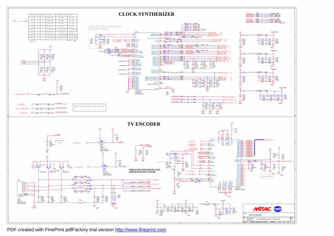
5
5
4
4
3
3
2
2
1
1
D D
C C
B B
A A
CLOCK SYNTHERIZER
33.33
1
Tristate1 66.66
100.00X
133.33
Mid
X66.66
1TCLK/2
Reserved
X01
X
PCI*
Mid
33.33
FS0
TCLK/2
UNIT: MHz1
Reserved
FS1
Reserved
010
Reserved
33.33
0
0
0:0V
TCLK/2Mid Tristate
1:3.3V
Tristate
FS2
0
166.66 33.33
0
Reserved
1
CPU 3V66[5:0]
1
66.66
Mid
66.66200.00
0
Reserved
001
Layout note: Place crystal within500 mils of CLK Gen.
TV ENCODER
Place nearto 7011.
Default NTSC
USE 20P 5%
WHEN USE INTEGRATE VGA R887/NA
WHEN USE INTEGRATE VGAADD R763 R766 U2 R1240
PCB 316680900001/ASSY 411680900011 R01
8050 MOTHER B/D
C
11 34Monday, December 29, 2003
Title
Size DocumentNumber
Rev
Date: Sheet of
FS1FS2
FS0
CLK_PCI_STOP#
VTT_PWRGD#
CLK_CPU_STOP#
CLK_PD#
HCLK_MCHHCLK_CPUITP_CPU
HCLK_MCH#
ITP_CPU#HCLK_CPU#
VTT_PWRGD#
FS1FS2
FS0
HCLK_CPU
ITP_CPU#
HCLK_CPU#
CLK_PCI_STOP#CLK_CPU_STOP#
CLK_PD#
HCLK_MCH#
ITP_CPUHCLK_MCH
TV_DDDA
TV_DDCK
DVOCD[0..11]
DVOCD7
855_TV_LUMA
DVOCD3
DVOCD6
DVOCD1
XOUT
DVOCD9DVOCD8
DVOCD10
DVOCD2
DVOCD4DVOCD5
DVOCD11
TV_DDCK
855_TV_CRMA
TV_DDDA
DVOCD0
XIN
PCICK_KBC
XIN
XOUT
PCICK_1394
PCICK_KBCPCICK_1394
DEFSSCLK
DEFSSCLK
855_TV_COMPCVBS1
855_TV_COMPCVBS1
DVOVREF
855_TV_CRMA
855_TV_LUMA
855_TV_COMP
CORE_CLKEN#31
SUSA#13
STOP_CPU#3,13,31
STOP_PCI#13
14M_CODEC 2014M_ICH 13
HCLK_CPU# 2
HCLK_CPU 2HCLK_MCH 4
CLK_ITP_CPU# 2
CLK_ITP_CPU 2
PCICLK_FWH 23PCICLK_MINIPCI 19PCICLK_CARD 17PCICLK_LAN 16
PCICLK_ICH 13
66M_MCH 466M_ICH 14
SMBDATA6,14SMBCLK6,14
HCLK_MCH# 4
USBCLK_ICH 14
MI2CCLK4
MI2CDATA4
DVOVREF4
DVOCCLK4DVOCCLK#4
DVOCHSYNC4DVOCVSYNC4
POUT/DET#4
DVOCFLDSTL4
TV_PCIRST#13
DVOBCINTR# 4
DVOCD[0..11] 4
66M_AGP 7
48M_DREFCLK 4
66M_DEFSSCLK 4
PCICLK_KBC 22
PCICLK_1394 18
SIO_48M 19
ATI_TV_LUMA 7
ATI_TV_CRMA 7
ATI_TV_COMP 7
+3V
GND +3V
GND
GND
GND
+3VCLK66
+3VCLKCPU
GND
+3V
+3V
+3VCLKANA
+3VCLKPCI
GND GND
GND
+3VCLKPCI
GND GND
+3V
+3V +3VCLK66
GND GND
+3V +3VCLKANA
GND GND
GND GND
+3V +3VCLKCPU
TV_GND
GND
TV_GND
GNDTV_GND
+3V
+3V
+3V
GND
+3V +3V
GND
GND
+3VA_TV
+3V
GND
+3V
GND
GND
GND
+3V+3V
GND
GND
+1.5V
+3V+3V
+3VA_TV
GND
GND
GND
GND
GNDGNDGND
GND GND
+3V
+3VGND
TV_GND
R892 49.9 0402 1%1 2
R478.2K/NA04025%
12
L726 120Z/100M 16081 2
C710.1U0402
50V+80-20%
12
C83010P/NA
040250V +/-10%
1 2
R8694.7K/NA04025%
12
C79110P0402
50V+/-10%
12
C420.1U0402
50V+80-20%
12
R7630 04021 2
R882 8.2K/NA0402
1 2
R704
01 2
R8484.7K04025%
12
C79610P0402
50V+/-10%
12
C17 33P0402 25V +/-10%
1 2
R895 33 0402 5%12
R818 33 04021 2
R8644.7K/NA04025%
12
C8020.1U0402
16V10%
12
R873 33 04021 2
D3BAV99/NA
123
R877 33 0402 5%12
C21270P0402
50V+/-10%
12
C610.1U0402
50V+80-20%
12
C79810P0402
50V+/-10%
12
C19 33P0402 25V +/-10%
1 2
C8030.1U0402
16V10%
12
C400.1U0402
50V+80-20%
12
D4BAV99/NA
123
R49330
04025%
12
C8200.1U0402
16V10%
12
L722 120Z/100M 16081 2
R467504025%
12
R861 33/NA 04021 2
RP275*41206
1234
8765
R37 1401 2
R8890/NA
0402 5%1 2
R688.2K04025%
12
R828 33 04021 2
L19120Z/100M
1 2
C640.1U0402
50V+80-20%
12
R52 1M/NA0402 5%
1 2
R807
10K04025%1
2
R56 0/NA0402 5%
1 2
R870 49.9/NA 04021 2
R830 8.2K/NA0402
1 2
C8220.1U0402
16V10%
12
C39
10U6.3V080510%
12
R8868.2K/NA
04021 2
R878 33 0402 5%12
C8090.1U0402
16V10%
12
R891 49.9 0402 1%1 2
R827 33 04021 2
R858 33 0402 5%1 2
C8010.1U0402
16V10%
12
R874 33 04021 2
R4875/NA04025%
12
U712
ICS950810TSSOP56284595081201
2
3
2534
43
53
562930
545540
3938
35
33
212223
24
26
28
14
1
1932
37
42
4650
8
49
15202731364147
567
10111213161718
514844
524945
X1
X2
*PD#PCI_STOP#
MULTSEL0*
CPU_STOP#*
REFSDATASCLK
FS0FS1FS2
48MHZ_USB48MHZ_DOT
3V66_1/VCH_CLK
3V66_0
66MHZ_OUT0/3V66_266MHZ_OUT1/3V66_366MHZ_OUT2/3V66_4
66MHZ_IN/3V66_5
VDDA
VTT_PWRGD#
VDDPCI1
VDDREF
VDD3V66_0VDD3V66_1
VDD48
IREF
VDDCPU0VDDCPU1
VDDPCI0
GND0GND1GND2GND3GND4GND5GND6GND7GND8
PCICLK_F0PCICLK_F1PCICLK_F2
PCICLK0PCICLK1PCICLK2PCICLK3PCICLK4PCICLK5PCICLK6
CPUCLKC0CPUCLKC1CPUCLKC2
CPUCLKT0CPUCLKT1CPUCLKT2
C79710P0402
50V+/-10%
12
C8270.1U0402
16V10%
12
R876
39004021%
1 2
C79310P/NA0402
50V+/-10%
12
C7882.2U0603+/-10%
12
C79510P0402
50V+/-10%
12
C82610P/NA0402
50V+/-10%
12
R865 33 04021 2
R872 33 04021 2
C78910P0402
50V+/-10%
12
J704
7P/RASUYIN33007S-07T1-C331870007007
123456
GND1GND2
7
123456
GND1GND2
7
C5220P0402
50V+/-10%
12
R935
10K04025%1
2
C7780.1U0402
16V10%
12
L20120Z/100M
1 2
R893 49.9 0402 1%1 2
R862 33/NA 04021 2
C79910P/NA0402
50V+/-10%
12
U2
CH7011APQFP64_0.5MM
291920212223242526272829303132
636261605958555453525150
78
3
45
10
13
1415
35
36
3738
39
42
43
46
47
48
5657
6 11 6416 1734 40 41
1833 44 1 12 4549
NC0NC1NC2NC3NC4NC5NC6NC7NC8NC9
NC10NC11NC12NC13NC14NC15
D[0]D[1]D[2]D[3]D[4]D[5]D[6]D[7]D[8]D[9]
D[10]D[11]
GPIO[1]GPIO[0]
VREF
HV
AS
RESET*
SPDSPC
ISET
CVBS
Y/GC/R
CVBS/B
XI/FIN
XO
P-OUT
BCO
C/HSYNC
XCLK*XCLK
DG
ND
_0D
GN
D_1
DG
ND
_2
AG
ND
_0A
GN
D_1
GN
D_0
GN
D_1
AG
ND
_2
AV
DD
_0
VD
D
AV
DD
_1
DV
DD
_0D
VD
D_1
DV
DD
V
DV
DD
_2
R826 33 04021 2
L25
120Z/100M 20121 2
R887 0/NA 0402 5%1 2
C79427P04025%
12
R7660 04021 2
R863 8.2K 04025%
1 2
C73
10U6.3V080510%
12
L718 120Z/100M 16081 2
R817 33 04021 2
C2392.2U0603+/-10%
12
C700.1U0402
50V+80-20%
12
DS
Q7122N7002SOT23_FET288227002006
G
DS
C79210P/NA0402
50V+/-10%
12
R881 0 0402 5%1 2
C8120.1U0402
16V10%
12
C8190.1U0402
16V10%
12
C20100P0402
50V10%
12
C8000.1U0402
16V10%
12
R875 33 04021 2
C5620P0402
50V+/-10%
12
C83410P/NA
040250V +/-10%
1 2
C15270P0402
50V+/-10%
12
L43 120Z/100M 16081 2
R8604.7K04025%
12
R6300805
12
C8112.2U0603+/-10%
12
R825 33 04021 2
R73 0/NA0402 5%
1 2
R821 0 0402 5%1 2
R871 49.9/NA 04021 2
C82510P/NA
040250V +/-10%
1 2
C782270P0402
50V+/-10%
12
R816 33 04021 2
R538.2K/NA04025%
12
R8534.7K/NA04025%
12
R824 33 04021 2
L56120Z/100M
1 2
D719
BAV99/NA
1 23
C430.1U0402
50V+80-20%
12
C38
10U6.3V080510%
12
C8210.1U0402
16V10%
12
R8880/NA
0402 5%1 2
R859 33 04025%
1 2
DS
Q7022N7002SOT23_FET288227002006
G
DS
C80427P04025%
12
C18100P0402
50V10%
12
R819 33/NA 04021 2
R5433004025%
12
C8232.2U0603+/-10%
12
R12400 04021 2
C2620.1U0402
16V10%
12
R820 0 0402 5%1 2
R8944.7K04025%
12
X701
14.318MHZ
TXC8X4.5
1 2
X703
14.318MHZ
TXC8X4.5
1 2
R83110K04025%
12
R890 49.9 0402 1%1 2
C344 33P0402 25V +/-10%
1 2
C83310P/NA
040250V +/-10%
1 2
C79010P0402
50V+/-10%
12
C530.1U0402
50V+80-20%
12
C670.1U0402
50V+80-20%
12
R71330/NA04025%
12
R829 33 04021 2
PDF created with FinePrint pdfFactory trial version http://www.fineprint.com
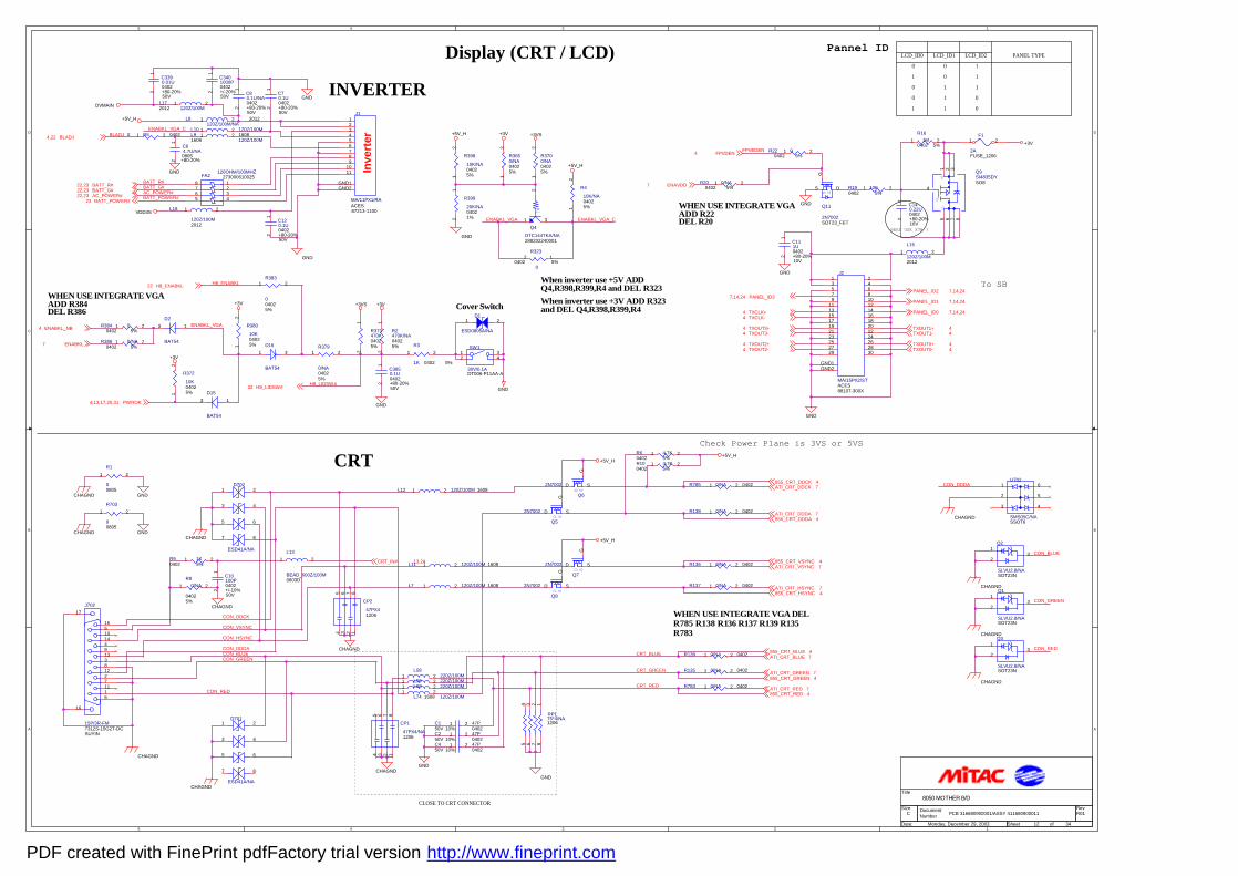
5
5
4
4
3
3
2
2
1
1
D D
C C
B B
A A
Check Power Plane is 3VS or 5VS
Display (CRT / LCD)0
1
1
01
PANEL TYPE
0
1
LCD_ID2LCD_ID1
1
1
LCD_ID0
INVERTER
Inve
rter
CRT
CLOSE TO CRT CONNECTOR
Pannel ID0
0 1
0 1 0
Cover Switch
WHEN USE INTEGRATE VGA DELR785 R138 R136 R137 R139 R135R783
WHEN USE INTEGRATE VGAADD R384DEL R386
To SB
WHEN USE INTEGRATE VGAADD R22
NEED USE X7R ?DEL R20
When inverter use +5V ADDQ4,R398,R399,R4 and DEL R323When inverter use +3V ADD R323and DEL Q4,R398,R399,R4
PCB 316680900001/ASSY 411680900011 R01
8050 MOTHER B/D
C
12 34Monday, December 29, 2003
Title
Size DocumentNumber
Rev
Date: Sheet of
ENABKL_VGA_C
CON_BLUE
CON_DDDA
CON_GREEN
CON_REDCON_DDDA
CON_HSYNC
CON_BLUECON_GREEN
H8_LIDSW#
H8_ENABKL
BATT_G#BATT_R#
BLADJ
CRT_GREEN
CON_DDCK
CRT_RED
CRT_BLUE
ENABKL_VGA
ENABKL_VGA ENABKL_VGA_C
CON_RED
CON_VSYNC
AC_POWER#BATT_POWER#
FPVEDEN
BLADJ4,22
BATT_R#22,23BATT_G#22,23
H8_ENABKL22
ENABKL_NB4
H8_LIDSW#22
ATI_CRT_GREEN 7
855_CRT_BLUE 4
855_CRT_GREEN 4
ATI_CRT_RED 7855_CRT_RED 4
ATI_CRT_BLUE 7
CRT_IN# 13,24
ATI_CRT_HSYNC 7855_CRT_HSYNC 4
855_CRT_VSYNC 4ATI_CRT_VSYNC 7
855_CRT_DDDA 4ATI_CRT_DDDA 7
855_CRT_DDCK 4ATI_CRT_DDCK 7
PWROK4,13,17,25,31
ENABKL7
AC_POWER#22,23BATT_POWER#23
TXOUT1+ 4
TXCLK+4
TXOUT1- 4
PANEL_ID2 7,14,24PANEL_ID37,14,24
PANEL_ID0 7,14,24TXCLK-4
FPVDEN4
PANEL_ID1 7,14,24
TXOUT0+ 4
TXOUT3+4TXOUT3-4
TXOUT2-4TXOUT2+4
TXOUT0- 4
ENAVDD7
GND
+5V_H
GND
+5V_H
+5V_H+5V_H
GND
CHAGND
CHAGND
CHAGND GND
CHAGND
CHAGND
CHAGND
CHAGND
GND
CHAGND GND
CHAGND
CHAGND
GND
+3VS
GND
+3V+3V
VDD3S
GND
CHAGND
+3VS
+5V_H
DVMAIN
CHAGND
+3V
GND
GND
+3V
GND
+3V
GND
+5V_H
R20 0/NA0402 5%
1 2
D15
BAT54
13
C10100P0402
50V+/-10%
12
L74 120Z/100M16081 2
R135 0/NA 04021 2
R384 00402 5%
1 2
R398
10K/NA04025%1
2
C3401000P0402
50V+/-20%
12
GD
S Q9SI4835DYSO8
876
4
51 32
Q1
SLVU2.8/NASOT23N
1
23
C111U0402
10V+80-20%
12
C64.7U/NA0805+80-20%
12
D701
ESD41A/NA
1 2
3 4
5 6
7 8
L12 120Z/100M 16081 2
RP175*4/NA1206
1234
8765
R380
10K04025%1
2
D16
BAT54
1 3
R138 0/NA 04021 2
L59 220Z/100M1 2R783 0/NA 04021 2
R4
10K/NA04025%1
2
C140.22U0402
16V+80-20%
12
C4 47P040250V 10%
1 2
R139 0/NA 04021 2
L7 120Z/100M 16081 2
C3390.01U0402
50V+80-20%
12
J1
MA/11PX1/RAACES87213-1100
123456789
1011
GND1GND2
D SQ7
2N7002
G
D S
L18
120Z/100M2012
1 2
L17120Z/100M2012
1 2
R10 4.7K0402 5%
1 2
R1
Q4
DTC144TKA/NA288202240001
2
1 3
R3700/NA04025%
12
R323
00402 5%
12
Q2
SLVU2.8/NASOT23N
1
23
Q3
SLVU2.8/NASOT23N
1
23
D S
Q5
2N7002
G
D S
D S
Q6
2N7002
G
D S
F1
2AFUSE_1206
1 2
C70.1U0402
50V+80-20%
12
R136 0/NA 04021 2
R161M
0402 5%1 2
L13
BEAD_600Z/100M0603D
1 2
FA2120OHM/100MHZ
27300061002512345
678
R50 04021 2
J2
MA/15PX2/STACES88107-300X
13579
11131517
246810121416182019
GND1GND2
2224262830
2123252729
R6 4.7K0402 5%
1 2
R19 10K0402 5%
1 2
C80.1U/NA0402
50V+80-20%
12
DS
Q11
2N7002SOT23_FET
G
DS
L15
120Z/100M2012
1 2
L10 120Z/100M1608
1 2
R383
004025%
1 2
D1
ESD0805A/NA
1 2
R3650/NA04025%
12
L11 120Z/100M 16081 2
U702
SMS05C/NASSOT6
1
2
3
6
5
4
R386 0/NA0402 5%
1 2
R399
20K/NA04021%
12
CP2
47PX41206
1234
8765
D2
BAT54
13
L58220Z/100M1 2
R22 00402 5%
1 2
SW1
30V/0.1ADT006-P11AA-A
12
34
R9 1K0402 5%
1 2
R379
0/NA04025%
1 2
R785 0/NA 04021 2
C120.1U0402
50V+80-20%
12
D702
ESD41A/NA
1 2
3 4
5 6
7 8
R1
00805
1 2
R703
00805
1 2
L60 220Z/100M1 2
R3
1K 0402 5%
1 2
C3850.1U0402
50V+80-20%
12
R80/NA
04025%
1 2
C1 47P040250V 10%
1 2
D S
Q8
2N7002
G
D S
L9120Z/100M1608
1 2
CP1
47PX4/NA1206
1234
8765
R373470K04025%
12
R2470K/NA04025%
12
L8120Z/100M/NA
20121 2
J702
15P/3R-FM7312S-15G2T-DCSUYIN
611172128313941410515
17
16
C2 47P040250V 10%
1 2
R137 0/NA 04021 2
R372
10K04025%1
2
PDF created with FinePrint pdfFactory trial version http://www.fineprint.com
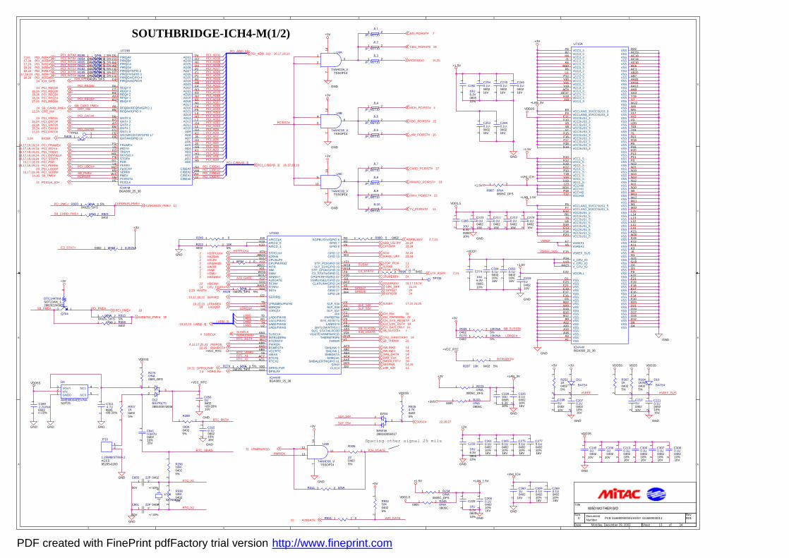
5
5
4
4
3
3
2
2
1
1
D D
C C
B B
A A
Spacing other signal 25 mils
SOUTHBRIDGE-ICH4-M(1/2)
PCB 316680900001/ASSY 411680900011 R01
8050 MOTHER B/D
C
13 34Monday, December 29, 2003
Title
Size DocumentNumber
Rev
Date: Sheet of
PCI_C/BE#[0..3]
PCI_C/BE#0PCI_C/BE#1PCI_C/BE#2PCI_C/BE#3
SB_PME#
PCI_LOCK#
PCIRST#
INTRUDER#
V5REF
V5REF
V5REF_SUS
V5REF_SUS
ICH_GPI5
PCI_REQ4#
PCI_REQ0#
CRT_IN#
PCI_GNT4#
PCI_GNT0#
PCIRST#
PWROK
SLP_S4#
SLP_S5#
LDRQ1#
SB_SUSST#
SB_CARD_PME#
PCI_PME#
PCI_AD0PCI_AD1PCI_AD2
PCI_AD[0..31]
PCI_AD3
PCI_AD5PCI_AD6PCI_AD7
PCI_AD4
PCI_AD9PCI_AD10
PCI_AD12
PCI_AD8
PCI_AD13
PCI_AD11
PCI_AD14PCI_AD15
PCI_AD17PCI_AD18
PCI_AD28
PCI_AD20
PCI_AD16
PCI_AD25PCI_AD26
PCI_AD24
PCI_AD31
PCI_AD21
PCI_AD19
PCI_AD29
PCI_AD27
PCI_AD30
PCI_AD22PCI_AD23
C3_STAT#
CARDBUS_PME#
PCI_PME#SB_PME#
SB_CARD_PME#
LAD0
SUSA#
LAD3LAD[0..3]
LAD1
SLP_S5#
RTC_X2
RTC_VBIAS
SUSCLK
HSTPCLK#
INTRUDER#
RTC_X1
LAD2
LDRQ1#
RTC_X1
SLP_S4#
RTC_RST#
A20_GATE
A20_GATE
ICH_VGATE
ICH_VGATE
C3_STAT#
RTC_VBIAS
SB_SUSST#
RTC_RST#
RTC_X2
GPIO27GPIO28
PCI_INTE#
PCI_INTB#
PCI_INTG#
PCI_INTD#
PCI_INTF#
PCI_INTA#
PCI_INTC#
PCI_REQ3#16,24PCI_REQ2#19,24PCI_REQ1#18,24
CRT_IN#12,24
PCI_GNT3#16,24PCI_GNT2#19,24PCI_GNT1#18,24
PCI_SERR#16,17,19,24
PCICLK_ICH11
VRMPWRGD31
HDPSLP#2,4DPRSLPVR14,31
RSMRST#22,25PWROK4,12,17,25,31
LAD[0..3]19,22,23
LFRAME#19,22,23
SERIRQ14,17,19,22
HINIT#2,23CPU_FERR#14HRCIN#22
HSMI#2
HINTR2HPWRGD2HSLP#2HA20M#2HSTPCLK#2
PCI_FRAME#16,17,18,19,24
PCI_PERR#16,17,18,19,24
PCI_IRDY#16,17,18,19,24
PCI_PAR16,17,18,19
PCI_TRDY#16,17,18,19,24
PCI_STOP#16,17,18,19,24
HNMI2
ICH_RI# 16
PCLKRUN# 16,17,19,24
CPUPERF# 24
STOP_CPU# 3,11,31SUSA# 11STOP_PCI# 11
WAKE_UP# 22,24SCI# 22,24
EXTSMI# 22,24KBD_US/JP# 22,24
MINIPCI_PCIRST# 19
CARD_PCIRST# 17
LAN_PCIRST# 16
KBC_PCIRST# 22
MCH_PCIRST# 4
1394_PCIRST# 18
ATI_PCIRST# 7
PCI_AD[0..31] 16,17,18,19
PCI_C/BE#[0..3] 16,17,18,19
AGPBUSY# 4,7,24
STP_AGP# 7,24
SBSPKR 14,20
ICH_LAN_RST# 14
SMLINK0 14
SMB_DATA 14
SMBALERT# 24
ICH_SYS_RESET# 14
SB_THRM# 22
SUSB# 17,22,23,25
14M_ICH 11
HIGNNE#2
SMLINK1 14
ICH_PWRBTN# 22
CPU_THRMTRIP# 14
ICH_BATLOW# 14
SMB_CLK 14
PCI_REQ4#24
SUSCLK4
PCI_GNT4#24
PCI_LOCK#24
PCI_GNT0#17,24
PCI_REQ0#17,24
PCIRST#0 15,25
FWH_PCIRST# 23
SB_SUSST# 7
TV_PCIRST# 11
A20GATE22
LRDQ0#19
CARDBUS_PME# 17
SB_CARD_PME#24
PCI_PME# 18
MINIPCI_PME# 19
SB_PME#14,16
GPIO27 24GPIO28 24
ICH_GPI524
SPK_OFF 21,24
PCI_INTA#7,24
PCI_INTC#17,24
PCI_INTG#18,24
PCI_INTD#19,24PCI_INTE#16,24PCI_INTF#17,19,24
PCI_INTB#17,24
PCI_DEVSEL#16,17,18,19,24
B/CB#3,24
SUSC# 22,26,27
GND
GND
GND
GND
GND
+VCC_RTC
+VCC_RTC
+3V
+LAN_3V
VDD3S
+1.5V
+VHI_ICH
+1.5V
+LAN_1.5V
GND
VDD1.5
GND
+5V +3V
GND
VDD5 VDD3S
+1.5V
GND
+VCCP
+3V +LAN_3V
GND
GND
+VHI_ICH
+1.5V
GND
+LAN_1.5V
VDD3S
GND
+3V
GND
GND
GND
GND
+3V
+3V
+3V
+3V
GND
+3V
VDD3S
GND
+3V
GND GND GND
GND
VDD5S
+1.5V
GND
VDD3S
+3V
+VCC_RTC
+3VS
VDD1.5
+3V
VDD5S
C2240.1U040216V
12
C2770.1U0402
16V10%
12
U715B
ICH4-MBGA360_25_36
D5C2B4A3C8D7C3C4
B6
B3C7
A2B1
A6B5
D6B7A7E6C1C5E8
F1L5F2
F3G1
U5
M2K5
L4
W2
P5
M3
P4D2R1D3P2E1P1E2M5E4N3E3N2E5N1F4F5L3H2L2G4L1G2K2J5H4J4G5K1H3J3H5
J2K4M4N4
PIRQA#PIRQB#PIRQC#PIRQD#PIRQE#/GPI0 2PIRQF#/GPIO 3PIRQG#/GPIO 4PIRQH#/GPIO 5
REQ# 4
REQ# 2REQ# 3
REQ# 1REQ# 0
REQB#/REQ5#/GPIO 1REQA#/GPIO 0
GNT# 4GNT# 3GNT# 2GNT# 1GNT# 0GNTB#/GNT5#/GPIO 17GNTA#/GPIO 16
FRAME#IRDY#TRDY#
STOP#PAR
PCIRST#
PLOCK#SERR#
PERR#
PME#
PCICLK
DEVSEL#
AD31AD30AD29AD28AD27AD26AD25AD24AD23AD22AD21AD20AD19AD18AD17AD16AD15AD14AD13AD12AD11AD10AD9AD8AD7AD6AD5AD4AD3AD2AD1AD0
C/BE#0C/BE#1C/BE#2C/BE#3
R805 0/NA 5%0402G_DFS1 2
C229
10U6.3V080510%
12
JL7
JP_NET101 2
R931 01 2
C2451U0402
10V
12
C3070.1U0402
16V10%
12
R920 0/NA 5%0402G_DFS1 2
C22810U
6.3V0805
10%
12
C2440.1U040216V
12
C8530.1U0402
16V10%
12
R240 01 2
U5
AME8800AEEV/NASOT25
123 4
5GND0VINVOUT NC1
NC0
C2080.1U0402
16V10%
12
R939 10K/NA0402 5%
1 2
C3114.7U0805+80-20%
12
D10
BAT54
13
D704
BAW56288100056017
2
13
U9B
74AHC08_VTSSOP14
4
56
147
C2530.1U040216V
12
R29610M04025%
12
U715A
ICH4-MBGA360_25_36
A5B2H6J1K6
M10P6U1
P12V10V16V18AC8
AC17H18J18
E9F9
E11F10V9V8V7
F15F16F17F18K14
K10K12K18K22P10T18V14U19L23
M14P18T22
F6F7
E12R6T6U6
G18E13F14E20
E7V6
E15
P14U18
AA23
C22
D1C23C21C19C17C15C6
B22B20B18B16B12B9
A22A20A18A16A4A1
D22AC23AC18AC14AC10AC5AC1AB20AB7AA22AA16AA12AA9AA3Y19Y7W22W8W5V17V15V3U20T23T19T1R21R18R5P22P20
D4
P13P11P3N23N21N19N14N13N12N11N10N5M13M12M11M1M22L21L14L13L12L11L10K23M20K19K13K11K3J6H1G21G19G6G3F8E22E21E19E18E17E16E14E10D23D21D19D17D15D12D8
VCC3_3VCC3_3VCC3_3VCC3_3VCC3_3VCC3_3VCC3_3VCC3_3VCC3_3VCC3_3VCC3_3VCC3_3VCC3_3VCC3_3VCC3_3VCC3_3
VCCLAN3_3/VCCSUS3_3VCCLAN3_3/VCCSUS3_3VCCSUS3_3VCCSUS3_3VCCSUS3_3VCCSUS3_3VCCSUS3_3VCCSUS3_3VCCSUS3_3VCCSUS3_3VCCSUS3_3VCCSUS3_3
VCC1_5VCC1_5VCC1_5VCC1_5VCC1_5VCC1_5VCC1_5VCC1_5VCCHI0VCCHI1VCCHI2VCCHI3
VCCLAN1_5/VCCSUS1_5VCCLAN1_5/VCCSUS1_5VCCSUS1_5VCCSUS1_5VCCSUS1_5VCCSUS1_5VCCSUS1_5VCCSUS1_5VCCSUS1_5VCCSUS1_5
V5REF1V5REF2
V5REF_SUS
V_CPU_IOV_CPU_IOV_CPU_IO
VCCPLL
VSSVSSVSSVSSVSSVSSVSSVSSVSSVSSVSSVSSVSSVSSVSSVSSVSSVSSVSS
VSSVSSVSSVSSVSSVSSVSSVSSVSSVSSVSSVSSVSSVSSVSSVSSVSSVSSVSSVSSVSSVSSVSSVSSVSSVSSVSSVSSVSSVSSVSS
VSS
VSSVSSVSSVSSVSSVSSVSSVSSVSSVSSVSSVSSVSSVSSVSSVSSVSSVSSVSSVSSVSSVSSVSSVSSVSSVSSVSSVSSVSSVSSVSSVSSVSSVSSVSSVSSVSSVSSVSSVSSVSSVSSVSSVSSVSSVSSVSSVSSVSSVSSVSS
R311 0/NA1 2
C2780.1U040216V
12
C2750.1U0402
16V10%
12
C292
10U6.3V080510%
12
C2601U0402
10V
12
R199 0/NA 5%0402G_DFS1 2
C3060.1U0402
16V10%
12
C8240.1U0402
16V10%
12
R2760/NA0805_DFS
12
R904 8.2K/NA0402 1 2
C2120.1U040216V
12
R880 0 04021 2
C2460.1U040216V
12
R2330/NA08050805C
1 2
C3150.1U0402
16V10%
12
R9080/NA0402
1 2
R867 0/NA0805C_DFS
1 2
R896 0 04021 2
U9C
74AHC08_VTSSOP14
9
108
147
D12BAV70LT1288100070006
1
23
C8410.047U0402
25V10%
12
JL1
JP_NET101 2
R93810M04025%
12
C2981U040210V
12
C2250.1U0402
16V10%
12
C233
10U6.3V080510%
12
R4090/NA
1 2
R288
180K04025%
1 2
D11
BAT54
13
R823 0/NA 5%0402G_DFS1 2
C2101U040210V
12
C3050.1U0402
16V10%
12
R195 0/NA 5%0402G_DFS1 2
C2130.1U0402
16V10%
12
C2690.1U0402
16V10%
12
R93210K04025%
12
C2110.1U040216V
12
J710
1.25MM/ST/MA-2ACES85205-0200
12
R2230/NA
0805C_DFS
1 2
R306
2204025%
1 2
JL6
JP_NET101 2
C2191U040210V
12
TP34 1
JL3
JP_NET101 2
C2230.1U040216V
12
R1641K/NA04025%
12
R934 01 2
C2070.1U0402
16V10%
12
R2450/NA08050805C
1 2
JL10
JP_NET101 2
R854 0/NA 5%0402G_DFS1 2
R1
Q704
DTC144TKASOT23AN_1288202240001
2
13
R9171K04025%
12
R287 10K 0402 5%
1 2
JL8
JP_NET101 2
X704
32.768KHZ
14
C2610.1U0402
16V10%
12
C8561U0402
10V+80-20%
12
R844 0/NA 5%0402G_DFS1 2
TP7051
R9264.7K04025%
12
C3040.1U0402
16V10%
12
C2940.1U040216V
12
C861 22P 0402
50V +/-10%
1 2
R3971K04025%
12
C274
10U6.3V080510%
12
C2061U0402
10V
12
R9280/NA
5%0402G_DFS1 2
U9A
74AHC08_VTSSOP14
1
23
147
R9150/NA5%0402G_DFS
1 2
R2521K04025%
12
R274 0/NA 5%0402G_DFS1 2
JL2
JP_NET101 2
U715D
ICH4-MBGA360_25_36
J19H19K20
AB23U21
AA21
W21
V22
AB22V21
W23
V23
U22Y22
Y23
J22
T2R4T4U2
U3U4
T5
AA4W6W7
Y6AC7AC6
AB6AA6AB5
V20U23
R2R3V4
V5W3
Y21W18W19T3Y20J21AC2V2W1W4
Y4Y2AA2Y1AA1Y3Y5AB2AB3V19W20V1
AC3AB1AB4AC4AA5H23J23
APICCLKAPICD_0APICD_1
A20M#CPUSLP#
FERR#
IGNNE#
INIT#
INTRNMISMI#
STPCLK#
RCIN#A20GATE
CPUPWRGD
SERIRQ
LAD0/FWH0LAD1/FWH1LAD2/FWH2LAD3/FWH3
LDRQ0#LDRQ1#
LFRAME#/FWH4
SUSCLKINTRUDER#RTCRST#
VBIASRTCX1RTCX2
PWROKRSMRST#VCCRTC
DPRSLPVRDPSLP#
AGPBUSY#/GPIO 6GPIO 7GPIO 8
GPIO 12GPIO 13
STP_PCI/GPIO 18SLP_S1#/GPIO 19
STP_CPU#/GPIO 20C3_STAT#/GPIO 21
CPUPERF#/GPIO 22SSMUXSEL/GPIO 23
CLKRUN#/GPIO 24GPIO 25GPIO 27GPIO 28
SLP_S3#SLP_S4#SLP_S5#
RI#PWRBTN#
SYS_RESET#LANRST#
BATLOW#/TP[ 0 ]SUS_STAT#/LPCPD
VGATE/VRMPWRGDTHERMTRIP#
THRM#
SMILINK 0SMLINK 1SMBDATA
SMBCLKSMBALERT#/GPIO 11
SPKRCLK14
C2892.2U/NA0603+/-10%
12
R270 10K/NA0402 5%
1 2
JL9
JP_NET101 2
R9210/NA0402
1 2
R192 0/NA 5%0402G_DFS1 2
C3080.1U0402
16V10%
12
JL5
JP_NET101 2
R2340/NA
0805C_DFS
1 2
JL4
JP_NET101 2
C285
10U6.3V080510%
12
C2210.1U0402
16V10%
12
C855 22P 0402
50V +/-10%
1 2
U9D
74AHC08_VTSSOP14
12
1311
147
R222 10K0402 5%
1 2
PDF created with FinePrint pdfFactory trial version http://www.fineprint.com
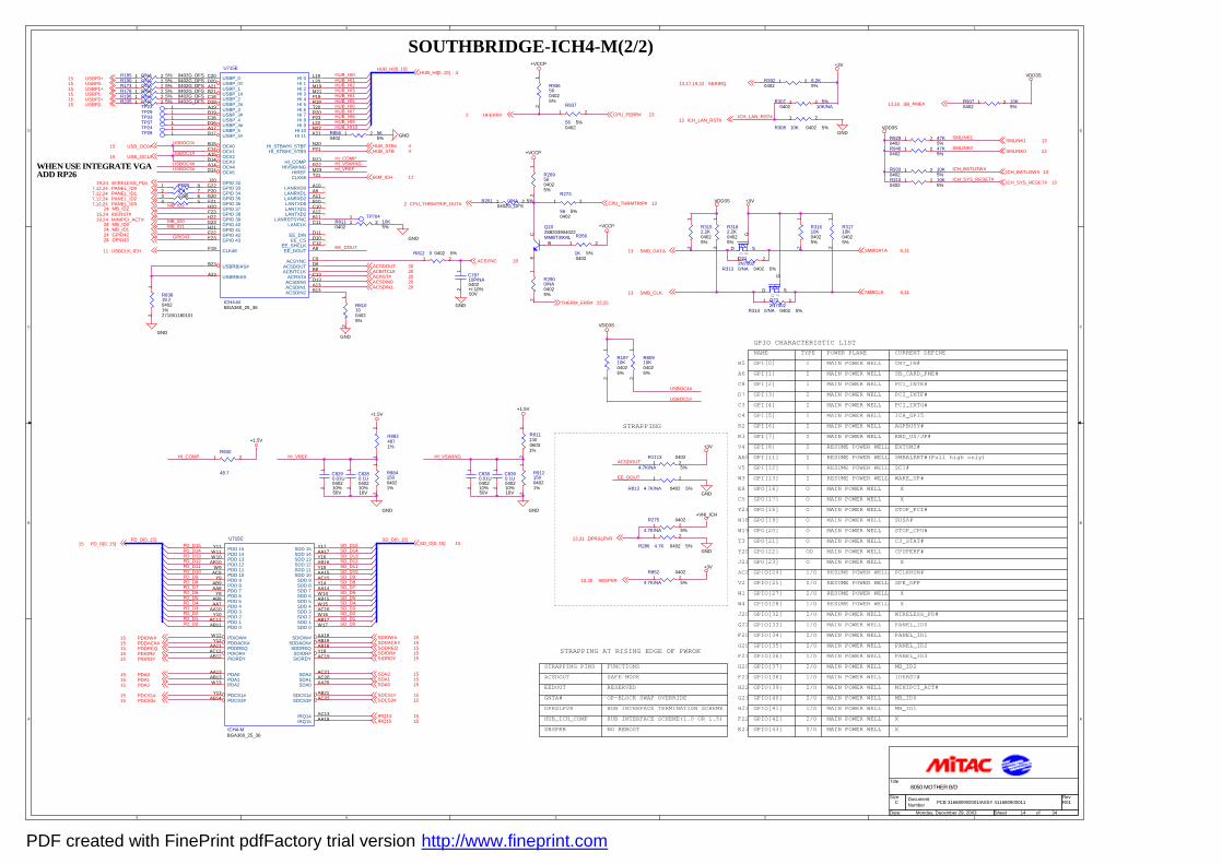
5
5
4
4
3
3
2
2
1
1
D D
C C
B B
A A
GPI[7]
GPIO[34]
GPO[17]
STOP_CPU#
GPIO[25]
MINIPCI_ACT#
RESUME POWER WELL
O
PANEL_ID0
GPO[18]
SBSPKR
STRAPPING PINS
GPI[0]
I
I/OGPIO[43]
I/O
GPIO[28]MAIN POWER WELL
I/O
I
O
CPUPERF#
MAIN POWER WELL
GPI[8]
MAIN POWER WELL
I/O
GPO[23]
GPIO[37]
GPIO[42]
I
RESERVED
GPIO[27]
GPO[19]
MAIN POWER WELL
GPI[2]
PCI_INTG#
MAIN POWER WELL
RESUME POWER WELL
I/O
MAIN POWER WELL
O
OP-BLOCK SWAP OVERRIDE
I
SMBALERT#(Pull high only)
GPIO[41]
PCLKRUN#
SUSA#
MAIN POWER WELL
RESUME POWER WELL
GPIO[32] I/O
MAIN POWER WELL
O
HUB INTERFACE TERMINATION SCHEME
I
MAIN POWER WELL
GPIO[39]
MAIN POWER WELL
MAIN POWER WELL
O
SPK_OFF
I/O
HUB INTERFACE SCHEME(1.0 OR 1.5)
MAIN POWER WELL
MAIN POWER WELL
GPIO CHARACTERISTIC LIST
I
GPIO[38]
GPI[11]
I
MAIN POWER WELL
GPIO[40]
GPO[20]
MAIN POWER WELL
GPIO[35]STRAPPING AT RISING EDGE OF PWROK
NO REBOOT
FUNCTIONS
CURRENT DEFINE
MAIN POWER WELL
MAIN POWER WELL
I
WAKE_UP#
MAIN POWER WELL
EXTSMI#
I/O
I/O
GPI[1]
RESUME POWER WELL
MAIN POWER WELL
EEDOUTI/O
I/O
GPI[3]
MAIN POWER WELL
I
NAME
MAIN POWER WELL
GNTA#
O
ACSDOUT
GPO[16]
I/O
MAIN POWER WELL
GPI[5]
TYPE
I/OGPIO[33]
I
KBD_US/JP#
SCI#
MAIN POWER WELL
DPRSLPVR
I
GPO[21]
I/O
GPI[6]
PANEL_ID1
O
GPIO[24]
GPI[13]
IDERST#
STOP_PCI#
I/O
MAIN POWER WELL
MAIN POWER WELL
RESUME POWER WELL
MAIN POWER WELL
AGPBUSY#STRAPPING
POWER PLANE
GPIO[36]
I
GPI[12]
RESUME POWER WELL
OD
RESUME POWER WELL
MAIN POWER WELL
HUB_ICH_COMP
MAIN POWER WELL
I/O
PANEL_ID2
GPO[22]
PCI_INTE#
RESUME POWER WELL
SAFE MODE
WIRELESS_PD#
PCI_INTF#
SB_CARD_PME#CRT_IN#
ICH_GPI5
C3_STAT#
X
XX
PANEL_ID3
XX
GPI[4]
B5A6C8D7C3C4R2R3V4AA5V5W3E8C5Y21W18W19T3Y20J21AC2V2W1W4J20G22F20G20F21H20F23H22G23H21F22E23
MB_ID2
MB_ID0MB_ID1
XX
SOUTHBRIDGE-ICH4-M(2/2)
WHEN USE INTEGRATE VGAADD RP26
PCB 316680900001/ASSY 411680900011 R01
8050 MOTHER B/D
C
14 34Monday, December 29, 2003
Title
Size DocumentNumber
Rev
Date: Sheet of
HUB_HI[0..10]
SD_D[0..15]PD_D[0..15]
HUB_HI0HUB_HI1
HUB_HI3HUB_HI2
HUB_HI7
HUB_HI5HUB_HI6
HUB_HI4
HUB_HI9HUB_HI10
HUB_HI8
EE_DOUT
SD_D15SD_D14
SD_D12SD_D13
SD_D10SD_D9
SD_D11
SD_D8
SD_D3
SD_D1
SD_D6SD_D5
SD_D7
SD_D2
SD_D0
SD_D4
PD_D0PD_D1PD_D2PD_D3
PD_D7
PD_D4
PD_D6PD_D5
PD_D11
PD_D8
PD_D15
PD_D12
PD_D10
PD_D13PD_D14
PD_D9
USBOC0#
USBOC4#USBOC5#
EE_DOUT
ACSDOUT
SMLINK0
ICH_BATLOW#
SMLINK1
ICH_LAN_RST#
ICH_SYS_RESET#
USBOC1#
USBOC4#
USBOC5#
MB_ID2
HI_VREF
HI_COMPHI_VSWING
HI_VSWINGHI_VREFHI_COMP
GPIO43
MB_ID1MB_ID0
USB_OC0#15
USB_OC1#15
WIRELESS_PD#19,24PANEL_ID07,12,24PANEL_ID17,12,24PANEL_ID27,12,24
IDERST#15,24MINIPCI_ACT#19,24
USBCLK_ICH11
PD_D[0..15]15
PDIOW#15PDDACK#15PDDREQ15PDIOR#15PIORDY15
PDA015PDA115PDA215
PDCS1#15PDCS3#15
SBSPKR13,20
DPRSLPVR13,31
SMB_CLK13
SMB_DATA13
CPU_THRMTRIP_OUT#2
HFERR#2ICH_LAN_RST#13
SERIRQ13,17,19,22
SMLINK1 13
SMLINK0 13
ICH_BATLOW# 13
ICH_SYS_RESET# 13
SMBDATA 6,11
SMBCLK 6,11
CPU_THRMTRIP# 13
CPU_FERR# 13
HUB_HI[0..10] 4
HUB_STB# 4HUB_STB 4
66M_ICH 11
ACSYNC 20ACSDOUT 20ACBITCLK 20ACRST# 20ACSDIN0 20ACSDIN1 20
SD_D[0..15] 15
SDIOW# 15SDDACK# 15SDDREQ 15SDIOR# 15SIORDY 15
SDA2 15SDA1 15SDA0 15
SDCS1# 15SDCS3# 15
IRQ14 15IRQ15 15
PANEL_ID37,12,24
USBP1-15USBP1+15USBP0-15USBP0+15
THERM_ERR# 22,25
SB_PME#13,16
MB_ID224
GPIO4324
MB_ID124MB_ID024
GPIO4224
USBP2+15USBP2-15
GND
GND
GND
+3V
GND
+VHI_ICH
GND
+VCCP
VDD3SGND
+3V
VDD3S
+3V
VDD3S +3V
+VCCP
+VCCP
VDD3S
GND
GND
+1.5V
+1.5V
+1.5V
GND
GND
C8380.01U0402
50V10%
12
R392 8.2K0402 5%
1 2
R813 4.7K/NA 0402 5%
1 2
TP28 1
R907 10K0402 5%
1 2
R19710K04025%
12
R852
4.7K/NA
0402
5%1 2
R185 0/NA 5% 0402G_DFS1 2
R173 0/NA 5% 0402G_DFS1 2
R937
560402
5%
1 2
R929 47K0402 5%
1 2
D S
Q212N7002
G
D S
R30710K/NA0402
5%1 2
R940 47K0402 5%
1 2
R266
1K0402
5%
1 2
R190 0/NA 5% 0402G_DFS1 2
R2900/NA04025%
12
R273
560402
5%
1 2
R196 0/NA 5% 0402G_DFS1 2
C78710P/NA0402
50V+/-10%
12
R261 0/NA 5%0402G_DFS1 2
Q20
MMBT3904L288203904022
B
EC
R91215004021%
12
R811 10K0402 5%
1 2
R933 10K0402 5%
1 2
TP33 1
RP260*41206
1234
8765
R8101004025%
12
R275
4.7K/NA
0402
5%1 2
R310 10K0402 5%
1 2
R83818.204021%271061180101
12
R8834871%
12
D S
Q222N7002
G
D S
R856 560402 5%
1 2
C8290.01U0402
50V10%
12
R205 0/NA 5% 0402G_DFS1 2
TP7041
U715E
ICH4-MBGA360_25_36
C20
A21
C18
A19
C16
D20
B21
D18
B19
D16
B15C14A15B14A14D14
J20G22F20G20F21H20F23H22G23H21F22E23
F19
B23
A23
L19L20M19M21P19R19T20R20P23L22N22K21
P21N20
R23R22M23T21
A10A9A11B10C10A12B11C11
D11D10C12A8
C9D9B8C13D13A13B13
A17B17
USBP_0
USBP_1
USBP_2
USBP_3
USBP_4
USBP_0#
USBP_1#
USBP_2#
USBP_3#
USBP_4#
OC#0OC#1OC#2OC#3OC#4OC#5
GPIO 32GPIO 33GPIO 34GPIO 35GPIO 36GPIO 37GPIO 38GPIO 39GPIO 40GPIO 41GPIO 42GPIO 43
CLK48
USBRBIAS#
USBRBIAS
HI 0HI 1HI 2HI 3HI 4HI 5HI 6HI 7HI 8HI 9
HI 10HI 11
HI_STB/HI_STBSHI_STB#/HI_STBF
HI_COMPHIVSWING
HIREFCLK66
LANRXD0LANRXD1LANRXD2LANTXD0LANTXD1LANTXD2
LANRSTSYNCLANCLK
EE_DINEE_CS
EE_SHCLKEE_DOUT
ACSYNCACSDOUTACBITCLK
ACRST#ACSDIN0ACSDIN1ACSDIN2
USBP_5USBP_5#
R1113
4.7K/NA
0402
5%1 2
R91113006031%
12
TP37 1
TP23 1
R88415004021%
12
TP24 1
TP29 1
R3182.2K04025%
12
R2695604025%
12
R9365604025%
12
R308 10K 0402 5%
1 2
R313 0/NA 0402 5%
1 2
R80910K04025%
12
C8390.1U0402
16V10%
12
R31710K04025%
12
R900
48.7
1 2
U715C
ICH4-MBGA360_25_36
AB11AC11
Y10AA10AA7AB8
Y8AA8AB9
Y9AC9W9
AB10W10W11Y11
W17AB17W16AC16W15AB15W14AA14Y14AC15AA15Y15AB16Y16AA17Y17
Y13 AB21AB14 AC22
AA13AB13W13 AA20
AC20AC21
AA11 AB18Y12 AB19
AC12 Y18
W12 AA18
AB12 AC19
AC13AA19
PDD 0PDD 1PDD 2PDD 3PDD 4PDD 5PDD 6PDD 7PDD 8PDD 9PDD 10PDD 11PDD 12PDD 13PDD 14PDD 15
SDD 0SDD 1SDD 2SDD 3SDD 4SDD 5SDD 6SDD 7SDD 8SDD 9
SDD 10SDD 11SDD 12SDD 13SDD 14SDD 15
PDCS1# SDCS1#PDCS3# SDCS3#
PDA0PDA1PDA2 SDA0
SDA1SDA2
PDDREQ SDDREQPDDACK# SDDACK#
PDIOR# SDIOR#
PDIOW# SDIOW#
PIORDY SIORDY
IRQ14IRQ15
R314 0/NA 0402 5%
1 2
R3152.2K04025%
12
R286 4.7K 0402 5%
1 2
R178 0/NA 5% 0402G_DFS1 2
R31610K04025%
12
C8280.1U0402
16V10%
12
R812 0 0402 5%1 2
PDF created with FinePrint pdfFactory trial version http://www.fineprint.com
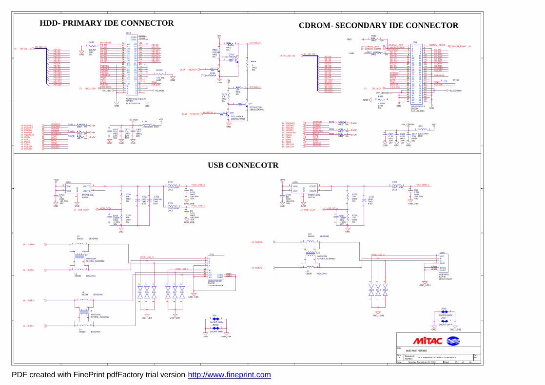
5
5
4
4
3
3
2
2
1
1
D D
C C
B B
A A
HDD- PRIMARY IDE CONNECTOR CDROM- SECONDARY IDE CONNECTOR
USB CONNECOTR
PCB 316680900001/ASSY 411680900011 R01
8050 MOTHER B/D
C
15 34Monday, December 29, 2003
Title
Size DocumentNumber
Rev
Date: Sheet of
PDA2
HDD_LED#
PD_D7RSTDRV1#
PDCS3#
PDA1
PD_D5
PD_D1PD_D2
IRQ14
PIORDY
PDDREQ
PD_D0
PDIOR#
PDCS1#
PD_D4
PDA0
PD_D6
PDDACK#
PDIOW#
PD_D3
PDDREQPDIOW#PDIOR#
PDDACK#IRQ14PDA1PDA0PDA2PDCS1#PDCS3#
PD_D12
PD_D8
PD_D10
PD_D13
PD_D15PD_D14
PD_D9
PD_D11
PIORDY
SDDREQ
SDIOR#
SDCS3#
SIORDYSDDACK#
SDCS1#
SDIOW#
SDA2SDA0SDA1IRQ15
SD_D[0..15]
PD_D4
PD_D12
PD_D6 SD_D3
SD_D1
PD_D11 SD_D8
SD_D5SD_D4
PD_D15
PD_D7
PD_D10
SD_D2
SD_D6
PD_D14
SD_D0
SD_D15
SD_D7
PD_D3
SD_D12
PD_D1
PD_D8
PD_D0
SD_D9SD_D10
PD_D2
PD_D13
PD_D5
PD_D9
SD_D11
PD_D[0..15]
SD_D13SD_D14
SD_D5
SDA1
SD_D3
SD_D8
SDA2
CD_LED#
RSTDRV2#SD_D7
SDIOW#
SDCS1#
CDROM_LEFT CDROM_RIGHT
SD_D14
SDCS3#
SD_D1
SDA0
IRQ15
SD_D9
SIORDY
SD_D11SD_D4
SD_D2
SDIOR#
SDDACK#
SD_D15SDDREQ
SD_D13
SD_D0
SD_D12
SD_D10SD_D6
CDROM_COMM
+VCC_USB_0
+VCC_USB_1
+VCC_USB_0
USB_OC1#
+VCC_USB_2
USB_OC0#
+VCC_USB_2
+VCC_USB_1
PCIRST#0
RSTDRV1#
RSTDRV2#
HDD_LED#23
PD_D[0..15]14
PDDREQ14PDIOW#14
PIORDY14PDIOR#14
IRQ1414PDDACK#14
PDA014PDA114
PDCS1#14PDA214
PDCS3#14
SDIOW#14
IRQ1514SDDACK#14
SDDREQ14
SDCS3#14
SDA114
SDA214SDCS1#14
SDIOR#14SIORDY14
SD_D[0..15]14
SDA014
CD_LED#23
CDROM_COMM20CDROM_LEFT20 CDROM_RIGHT 20
USB_OC0#14
USBP2+14
USBP1+14
USBP1-14
USBP0+14
USBP0-14
USB_OC1#14
USBP2-14
PCIRST#013,25
IDERST#14,24
GNDGND
GND
+5V_HDD
GND
+3V
+3V
+3V
+3V
+3V
+3V
+5V_CDROM
GND
GND
GND
GND
GND
GND_USB1
GND_USBGND_USB1
GND_USB
GND_USB
GND
GND_USB
+5VS
GND_USBGND
GND
GND
+5VS
GND_USB1GND
GND
GND_USB
GND
GND
GND_USB1
GND
+5V
+5V
GND
+5V_HDD
GNDGND
+5V_HDD
GND
+5V_CDROM
GND
+5V
GND
+5V_CDROM
GND
+5V
L733
120Z/100M 20121 2
JO17
SHORT-SMT4
1 2
JO15
12
C81710U
10V0805C
12
R70633K04025%
12
R1081 4.7K0402 5%
1 2
U701
RT9701-CBLSOT25
1
2
3
4 5
VOUT0
GN
D
VIN0
VIN1 VOUT1
J706
USB/4PX1SUYIN2545A-04GXT
1234
GND1GND2
VCCP-P+GND
GND1GND2
R834 8.2K0402 5%
1 2 C8160.1U0402
16V10%
12
C7091U0402
10V+80-20%
12
C8720.1U0402
16V10%
12
R70133K04025%
12
JO13
SHORT-SMT4
1 2
+C701
150U73436.3V
12
R47610K04025%
12
L723
120Z/100M2012
1 2
L708
120Z/100M2012
1 2
J708
R/A-25PX2/0.8SPEEDK22-102-150X
13579
1113151719212325272931
35373941434547
24681012141618202224262830323436384042444648
33
49 50
135791113151719212325272931
35373941434547
2468
1012141618202224262830323436384042444648
33
49 50
+C702
150U/NA73436.3V
12
R90110K/NA04025%
1 2
JO5
12
JO3
12
R1 Q41
DTC144TKA288202240001
2
13
C7031U0402
10V+80-20%
12
R927 10K/NA0402 5%
1 2
C8770.1U0402
16V10%
12
C50.1U0402
50V+80-20%
12
L3BEAD/NA0603D
1 2
R92210K0402 5%
1 2
L1BEAD/NA0603D
1 2
R1
Q703DTC144TKA/NA
2
13
C7041000P0402
50V+/-20%
12
R879 5.6K/NA0402 5%
1 2
R1074 8.2K0402 5%
1 2
C7111000P0402
50V+/-20%
12
+C713
150U73436.3V
12
90Z/100MCHOKE_ACM2012
L2
21
34
C8130.1U0402
16V10%
12
JO14
12
JO702
SHORT-SMT4
1 2
R909
004025%1
2
R91910K/NA04025%
12
L23BEAD/NA0603D
1 2
J701
USB/4PX2/DIPSUYIN2522A-08G1T-K
1234
A1A2A3A4
GND1GND2
1234
A1A2A3A4
GND1GND2
C87810U
10V0805C
12
L4BEAD/NA0603D
1 2
U705
RT9701-CBLSOT25
1
2
3
4 5
VOUT0
GN
D
VIN0
VIN1 VOUT1
L702
120Z/100M2012
1 2
C30.1U0402
50V+80-20%
12
90Z/100MCHOKE_ACM2012
L5
21
34
R70847K04025%
12
JO9
SHORT-SMT4
1 2
R833 4.7K0402 5%
1 2
JO16
12
R295 5.6K/NA0402 5%
1 2
JO4
12
L21BEAD/NA0603D
1 2
R836
470/NA04025%
1 2
R1085
4700402
5%
1 2
JO8
12
L6BEAD/NA0603D
1 2
L701
120Z/100M2012
1 2
R436
10K/NA04025%
1 2
R49210K04025%
1 2
JO7
12
R70247K04025%
12
90Z/100MCHOKE_ACM2012
L22
21
34
JO6
12
C310.1U0402
50V+80-20%
12
R1 Q37
DTC144TKA288202240001
2
13
J714
HDR/FM/22PX2/2MMSPEEDACE-1A2-0216
135791113151719212325272931333537394143
2468
101214161820222426283032343638404244
GND1GND2
13579
1113151719212325272931333537394143
2468101214161820222426283032343638404244
GND1GND2
R1
Q705DTC144TKA/NA
2
13
TP7061
PDF created with FinePrint pdfFactory trial version http://www.fineprint.com
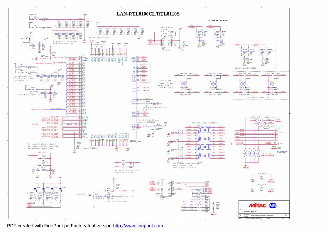
5
5
4
4
3
3
2
2
1
1
D D
C C
B B
A A
LAN-RTL8100CL/RTL8110S
Change to 2.49K when useRTL8110S
3.Not to use via
USED IN 93C56
1.50/8/8/8/502.Parallel andequal length
It's should be NA whenchange to RTL8110S
ADD if use RTL8110S
Change DVDD to +1.8VS,when use RTL8110S
ADD if use RTL8110S
Close to RTL8100C
ADD if use RTL8110S
ADD if use RTL8110S
GND_45
Change AVDDL to+2.5VS_DDR , whenuse RTL8110S
GND_45
ADD if use RTL8110S
Crystal should be placedfar away from I/O port andTx,Rx,power,magnetics.
GND_45
GND_45
GND_45
GND_45
GND_45
Pull high at EC side.
Add AVDDL to V_DAC, whenchange to RTL8110S
Add thease caps whenuse RTL8110S, andC879 change to 0.01U
Use H1285 for RTL8100C
PCB 316680900001/ASSY 411680900011 R01
8050 MOTHER B/D
C
16 34Monday, December 29, 2003
Title
Size DocumentNumber
Rev
Date: Sheet of
MDI0-
EEDO
PCI_AD12MDI3-
PCI_AD0
PCI_AD22
PCI_AD25
PCI_AD1
PCI_C/BE#3
PCI_AD20
EEDI
PCI_AD14
EECS
CTRL18
PCI_AD21
PCI_AD27
PCI_AD9
V_12P
PCI_AD19
MDI3+
PCI_AD5
PCI_AD15PCI_AD16
PCI_AD13
PCI_AD6
MDI2+
LAN_XTAL1PCI_AD17
PCI_AD23
EECK
MDI0+
PCI_AD8
PCI_AD18
PCI_AD10 MDI2-
LAN_XTAL2
MDI1+
PCI_AD24
PCI_AD4PCI_AD3
PCI_AD11
PCI_AD26
PCI_AD7 MDI1-
ISOLATEB
PCI_AD18
PCI_AD2
DVDD
CTRL18
LAN_WAKE
MDI2+ MDI3+MDI3-MDI2-
MDI0- MDI1-MDI0+ MDI1+
MDI2+
MDI2-
MDI3+
MDI3-MDI1-MDI0-
MDI1+MDI0+
MODEMN
MDO3-
MDO2-
MDO3+
AVDDL
EECKEECS
EEDOEEDI
LED3
LED1LED0
LED2
PCI_C/BE#2
PCI_C/BE#0
PCI_AD30PCI_AD29PCI_AD28
PCI_C/BE#1
PCI_AD[0..31]
PCI_AD31
PCI_C/BE#[0..3]
MCT4
MCT3
MDO3-MDO3+
MDO2+MDO2-
MCT2
MCT4
MCT3
MCT1
V_DAC
V_DAC
PMDI0-
PMDI0+
PMDI1+
PMDI1-
LAN_XTAL2
LAN_XTAL1
LED2
LED0
LED3
LED1
MODEMP
MDO2+PJRX+
PJRX+
LAN_WAKE
AVDDL
DVDD
V_DAC
V_DAC
MDO3-
PMDI0-
V_DAC
PMDI1-
PJRX+
PMDI3+
MCT1
MDO2-
PJRX-
PMDI2+ MDO2+
MCT3
PMDI2-
PMDI3-
MCT2
PMDI1+
MDO3+
PMDI0+
MCT4
V_DAC
V_DAC
PMDI2+
PMDI2- PMDI3-
PMDI3+PMDI1+
PMDI1-PMDI0-
PMDI0+
PJRX-
PJTX+
PJRX-
PJTX1-
PJTX+
PJTX+PJTX-PJTX1-
PJTX1-
PCI_AD[0..31]13,17,18,19
PCI_REQ3#13,24
PCI_SERR#13,17,19,24
PCI_TRDY#13,17,18,19,24
PCI_DEVSEL#13,17,18,19,24
PCI_INTE#13,24
PCI_FRAME#13,17,18,19,24
PCI_PAR13,17,18,19
PCI_IRDY#13,17,18,19,24
PCI_STOP#13,17,18,19,24LAN_PCIRST#13
PCI_GNT3#13,24
PCICLK_LAN11
PCI_C/BE#[0..3]13,17,18,19
PCI_PERR#13,17,18,19,24
PCLKRUN#13,17,19,24
SB_PME#13,14
MODEMP20MODEMN20
KBC_RI# 22
ICH_RI# 13
DVDD
+5V
+3VS
GND
GND
DVDD_A
GND
GND
AVDDH
DVDD
AVDDL
GND
+3VS
GND
GND
+1.8VS
+2.5VS_DDR DVDD
GND
+1.8VS
+3VS
GND
+3VS
GND
AVDDH
GND
GND
GND
GND
AVDDL+2.5VS_DDR
GND
+3VS
+3VS
GND
GND GND +3V
GND
GND
+3VS
GND
GND
GND
GND
GND
JO716
12
C8350.1U0402
12
C9050.1U0402
16V10%
12
C8670.1U040216V10%
12
JO71812
C889
0.1U040216V10%
12
R106349.9/NA04021%
12
C9000.01U0402
50V+80-20%
12
R1114
0/NA0402 5%
1 2
C8630.1U0402
16V10%
12
C8830.1U0402
16V10%
12
C8790.1U0402
16V10%
12
R1107510/NA04021%
12
R1097510/NA04021%
12
R108249.904021%
12
R262 75/NA0402
1 2
R9430/NA0805
12
Q707
2SB1188/NA
B
EC
R10995.6K0402
1%
1 2
C8800.1U0402
16V10%
12
C8840.01U/NA0402
50V+80-20%
12
R1 Q709
DTC144TKA288202240001
2
13
C8730.1U0402
16V10%
12
L51
120Z/100MCORE_ACM2520U
14
23
JO715
12
C9030.1U/NA0402
16V10%
12
JO71912
L72800603
1 2
U716
H5007/NAH500X
1
2
3
24
23
22
4
5
6
21
20
19
7
8
9
10
11
12 13
14
18
17
16
15
D709
CL-190G/NA
AK
X706
25MHZTXC8X4.5274012500415
1 2
JO72012
JO717
12
R9440/NA0805
12
U719
RTL8100CLPQFP128A_0.5MM
127
113114115117
8125
121
122
12
56
1415
1819
3123
105
3334363739404243474950535557585979828385868789909395969798
102103104
111109108106
24 32 45 54 64 78 99 110
116
126
26 41 56 71 84 94 107
3 7 16 20 10 120
22 35 48 52 62 73 80 100
112
118
21 38 51 66 81 91 101
119
13 17 9 4 123
124
128
11127274
92776044
28656861293046256367768870756927
RSET
NC_14LED2LED1LED0
CTRL25NC_13
XTAL1
XTAL2
TX+TX-
RX+RX-
NC_9NC_10
NC_11NC_12
PMEBISOLATEBLANWAKE
AD31AD30AD29AD28AD27AD26AD25AD24AD23AD22AD21AD20AD19AD18AD17AD16AD15AD14AD13AD12AD11AD10AD9AD8AD7AD6AD5AD4AD3AD2AD1AD0
EESKAUX/EEDI
EEDOEECS
NC
_18
VD
D25
_0N
C_1
9V
DD
25_1
NC
_20
VD
D25
_2V
DD
25_3
NC
_21
NC
_22
NC
_23
VD
D33
_0V
DD
33_1
VD
D33
_2V
DD
33_3
VD
D33
_4V
DD
33_5
VD
D33
_6
AV
DD
33_0
AV
DD
33_1
NC
_24
AV
DD
33(R
EG
)
NC
_25
NC
_26
NC
_0G
ND
_0N
C_1
GN
D_1
NC
_2N
C_3
GN
D_2
GN
D_3
NC
_4N
C_5
GN
D_4
GN
D_5
GN
D_6
GN
D_7
GN
D_8
GN
D_9
GN
D_1
0G
ND
_11
NC
_6G
ND
_12
NC
_7G
ND
_13
GN
D_1
4G
ND
_15
GN
D_1
6
NC_15AVDD25
NC_16NC_17
CBEB0CBEB1CBEB2CBEB3
PCICLKCLKRUNBDEVSELBFRAMEBGNTBREQBIDSELINTABIRDYBTRDYBPARNC_8PERRBSERRBSTOPBPCIRSTB
C8940.1U0402
16V10%
12
L732120Z/100M2012
1 2
R303 0/NA 06031 2
JO721
12
C87010U16V1206
12
L71900603
1 2
C8960.01U0402
50V+80-20%
12
C8450.01U/NA0402
12
R109049.904021%
12
C9060.1U0402
16V10%
12
L735
120Z/100M2012
12
R271750402
1 2
R1111
00402
5%1 2
C3271000P2KV
10%1808
12
L736
120Z/100M/NA2012
1 2
C8950.1U0402
16V10%
12
C8650.1U0402
16V10%
12
C8900.1U/NA0402
16V10%
12
U717
LF-H80PSOX16
768
10119
132
161415
45
1213
TD+TDCTD-
TX+TXCTX-
RD+RDCRD-
RX+RXCRX-
NC0NC1
NC2NC3
R110810K/NA0402
1 2
R297 0/NA 0603
1 2
R277750402
1 2
D707
CL-190G/NA
AK
R10701K/NA04025%
12
U723
93C46SO8283467540002
1234 5
678CS
SKDIDO GND
NC0NC1VCC
R106749.9/NA04021%
12
C8540.01U/NA0402
12
R263 0/NA 0603
1 2
C9111U0402
10V+80-20%
12
C8870.1U0402
16V10%
12
D708
CL-190G/NA
AK
R278 0/NA 0603
1 2
R1109510/NA04021%
12
R108749.904021%
12
L48
120Z/100M/NACORE_ACM2520U
14
23
C8930.1U0402
16V10%
12
C8740.1U0402
16V10%
12
R107149.9/NA04021%
12
R930 750402
1 2
R254 75/NA0402
1 2
R111510K04025%
12
L737120Z/100M2012
1 2
R1100
0/NA 0402
1 2
R106649.9/NA04021%
12
C8640.1U0402
16V10%
12
L738120Z/100M/NA2012
1 2
D710
CL-190G/NA
AK
R285 0/NA 06031 2
R272 0/NA 06031 2
C91527P04025%
12
C8820.01U/NA0402
50V+80-20%
12
R108649.904021%
12
C8760.1U0402
16V10%
12
L731120Z/100M/NA2012
1 2
R100815K 0402
12
C91427P04025%
12
C8620.1U0402
16V10%
12
C8860.1U0402
16V10%
12
R10061K0402
12
C8910.1U0402
16V10%
12
RP270*41206
1234
8765
R11103.6K0603
1 2
C8660.1U0402
16V10%
12
R1102510/NA04021%
12
R305 0/NA 06031 2
R1101
1M0402 1%
12
L49
120Z/100MCORE_ACM2520U
14
23
RJ45
RJ11
J709
RJ11-2P/RJ45-8PC10037-102XX
GND1GND2
A2A1
87654321
GND1GND2
A2A1
87654321
L44
120Z/100M/NACORE_ACM2520U
14
23
R152 750402
1 2
C8490.01U/NA0402
12
C9040.1U0402
16V10%
12
R304 0/NA 0603
1 2
JO714
12
R947 100 04021 2
PDF created with FinePrint pdfFactory trial version http://www.fineprint.com
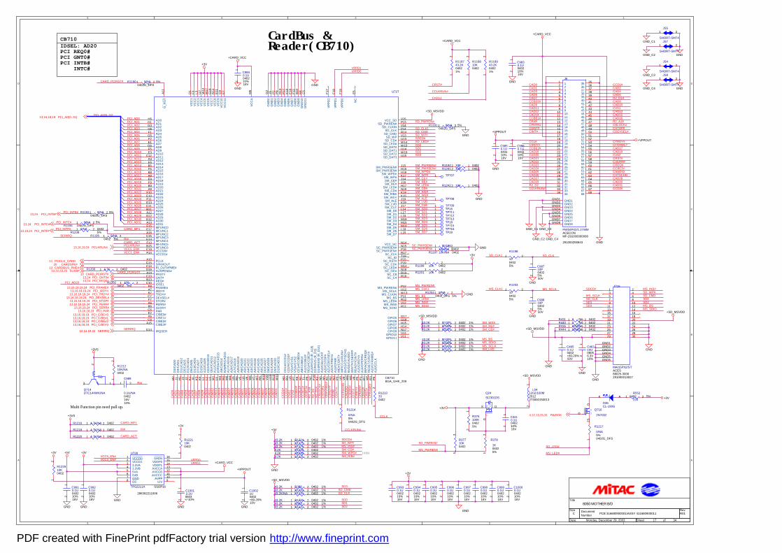
5
5
4
4
3
3
2
2
1
1
D D
C C
B B
A A
CB710
(43K)
Multi Function pin need pull up.
IDSEL: AD20PCI REQ0#PCI GNT0#PCI INTB# INTC#
CardBus &Reader(CB710)
PCB 316680900001/ASSY 411680900011 R01
8050 MOTHER B/D
C
17 34Monday, December 29, 2003
Title
Size DocumentNumber
Rev
Date: Sheet of
PCI_AD[0..31]
SD_CLK1
PCI_AD6
PCI_AD24
PCI_AD3
VCC5_EN#
MS_SDIO
SM_CE#
SD_LED#
SD_CMD
SD_CMD
VCC3_EN#
CD
EV
SE
L#
CC
BE
2#
CV
S2
CA
D25
CA
D24
SERIRQ
PCI_AD0
SM_WP#
SM_SD2
SD_CLK
SD2SD3
CFR
AM
E#
CC
D2#
PCI_AD5
SERIRQ
CARD_ACT
VCC3_EN#
MS_PWREN#
MS_INS#
CR
EQ
#
R2_
A18
CA
D10
CA
D2
PCI_AD19
PCI_AD10
CARD_MF1
CCLKRUN#
MS_LED#
SM_LVD
SM_SD6
SM_WPD#
CP
ER
R#
CTR
DY
#
CA
D17
CA
D8
PCI_AD8
PCI_AD12
RI#
SM_SD1
SD_WP#
CS
TOP
#
CA
D9
CA
D5
PCI_AD2
PCI_AD23
PCI_AD27
PCI_AD4
SM_ALE
SM_SD3
CARD_PCIRST#
CCLKRUN#
CA
D30
CA
D11
PCI_AD25
VPPD1
MS_INS#
SM_PWR3EN#
CB
LOC
K#
PCI_AD17
MS_CLK1
SDCD#
SD1
CR
ST#
CA
UD
IO
R2_
D14
CV
S1
CA
D18
CA
D20
PCI_AD21
PCI_AD14
PCI_AD20
PCI_AD13
PCI_AD16
SM_RE#
SD_WP#
VPPD1
CA
D29
CA
D28
CA
D1
PCI_AD29
PCI_AD15
CRST#
SM_PWR5EN#
SM_R/B#
SM_CLE
SM_SD4
SD_PWREN#
SM_R/B#
VPPD0
CS
TSC
HG
CP
AR
CC
BE
1#
CA
D13
CA
D12
CA
D4
PCI_AD9
SM_CD#
SD_CLK1
SD3
SDCD#
SD0
SD0
CCLK
CIR
DY
#
CC
BE
0#
CC
D1#
CA
D19
CA
D16
PCI_AD11
SM_SD0
SM_SD7
SD2
SM_CD#
CARD_ACT
CIN
T#
CA
D21
CA
D6
PCI_AD18
PCI_AD20
CARD_MF1
CA
D14
PCI_AD30
VPPD0
SD1
PCI_AD31
PCI_AD22SM_WE#
CG
NT#
CC
BE
3#
CA
D27
CA
D31
CA
D3
CA
D0
CARD_PCIRST#
PCI_AD28
RI#
SM_WPD#
SM_SD5
CS
ER
R#
R2_
D2
CA
D22
CA
D23
PCI_AD7
PCI_AD26
PCI_AD1
CAD11
CA
D26
CA
D15
CA
D7
SC_PWR5EN#SC_PWR3EN#
RI#
PCI_INTB#
PCI_INTC#
SD_PWREN#
MS_PWREN#
MS_CLK1
SM_RE#SM_CE#
SM_WE#
CAD30
CAUDIO
CDEVSEL#
CAD10
R2_D2
CAD11
CCBE1#
CAD7
CAD28
CTRDY#
CAD8
CAD23
CPERR#
CVS2CAD19
CCLKRUN#
CAD0
CAD17
R2_D14CCBE0#
CAD5
CSERR#
CAD26
CPARCBLOCK#
CAD2
CCBE3#CREQ#
CAD24
CAD22
CAD18
CIRDY#
CAD12
CAD9
CAD1
CFRAME#
CCD1#
CAD21
CCLK
CINT#
CAD3
CVS1
CAD4
CCD2#
CSTOP#
CAD13
CAD27
CAD14
R2_A18
CAD15
CAD20CRST#
CCBE2#
CGNT#
CAD31
CAD6
CSTSCHG
CAD16
CAD29
CAD25
SD_LED#
MS_LED#
PCLKRUN#VCC5_EN#
SD_WP#MS_INS#
SD2
MS_SDIO
SM_LVD
MS_SCLK
MS_SCLK
MS_BS
MS_BS
PCI_INTF#
SD_CLK
SDCD#
SD_CLKSD1SD3
MS_SCLK
MS_SDIOMS_BS
SD_CMDSD0
SM_LED#
PCI_AD[0..31]13,16,18,19
PCI_INTB#13,24
PCI_C/BE#213,16,18,19PCI_C/BE#313,16,18,19
PCI_C/BE#013,16,18,19PCI_C/BE#113,16,18,19
PCI_REQ0#13,24PCI_GNT0#13,24
PCI_TRDY#13,16,18,19,24
PCI_FRAME#13,16,18,19,24
PCI_PERR#13,16,18,19,24PCI_SERR#13,16,19,24
PCI_DEVSEL#13,16,18,19,24
PCI_IRDY#13,16,18,19,24
PCI_STOP#13,16,18,19,24
PCI_PAR13,16,18,19
CARD_PCIRST#13SUSB#13,22,23,25
PCLKRUN#13,16,19,24
SERIRQ13,14,19,22
PCICLK_CARD11CARDSPK#20
CARDBUS_PME#13
PWROK4,12,13,25,31
PCI_INTC#13,24
PCI_INTF#13,19,24
GND
+SD_MSVDD
+CARD_VCC
+3V
+5V
GND
GND
GND
GND
+VPPOUT
+CARD_VCC
GND
+3V
+CARD_VCC
GND
+3V
GND
+3V
GND
GND
+VPPOUT
+3V
GND
+CARD_VCC
+3VS
+3V
GND
GND
+VPPOUT
GND
GND
+SD_MSVDD
GND
+3VS
GND
+SD_MSVDD
GND
+3V
+SD_MSVDD
+3V
GND_C3
GND_C2
GND
GND_C1
GND
GND_C4
GND_C1
GND_C2 GND_C4
GND_C3
GND
GND
GND
GND
+SD_MSVDD
+SD_MSVDD
+3V
GND
TP7131
R122910K0402
12
R1195 0/NA0402 5%1 2
C46310U
6.3V0805
10%
12
C9960.1U0402
16V10%
12
C10021U0402
10V+80-20%
12
R378
1K04025%1
2
R121043.2K 0402 1%1 2
U727
CB710BGA_GHK_209
H5G1G3H6F1G5F2E1G6F5E3
C12A4E6B5F6B8A8E9F9B9A9
F10E10F11E13C11B11A12B12E12A13F15E17A16C15E14F13B15E19
A10
F14
F17
G15C14D19A14C13B13C10
F8A7B7C7F7A6B6C6E2A5C8
A15
R8
W7
V7
W6
V6
U6
V5
U5
N1
M3
L1 M1
T1 N3
P1
P5
P6
M6
N2
N6
N5
R1
R2
R3
W4
R6
W10
U10
P10
H2
J1 J3 K1
K3
V10
R10
W11
H1
J2 J6 K2
K5
H3
R9
K6
L2 L6 L5 M2
P3
U9
V9
W9
W8
V8
U8
P7
P8
R7
W5
J19
K14K15
K19
L15
L17L19
M15
W16
R14
W14
P14
N18
R17
N14
M14
P18
U15
T19P15
R18
P17
P19
N17
N19
M18
H14
G18
G14U11
R11
U12
R12
V13
H15
G17
F19
P11
V12
P12
W13
U13
V11
H17
P13
R13
J18
M19
U14W15
V15
R19
L18
H18H19J15
J14
J17
K17
L14
D1
E11
F3 L3 U7
W12
N15
G19
B14
A11
C9
E7
F18
M17
M5
G2
J5 P2
P9
V14
K18
E18
F12
B10
E8
C5
E5
AD0AD1AD2AD3AD4AD5AD6AD7AD8AD9AD10AD11AD12AD13AD14AD15AD16AD17AD18AD19AD20AD21AD22AD23AD24AD25AD26AD27AD28AD29AD30AD31MFUNC0MFUNC1MFUNC2MFUNC3MFUNC4MFUNC5MFUNC6VCCD0#
PCLK
VCCD1#
VP
PD
2
SPKROUTRI_OUT#PME#SUSPEND#PRST#GNT#REQ#IDSELFRAME#IRDY#TRDY#DEVSEL#STOP#PERR#SERR#PARC/BE0#C/BE1#C/BE2#C/BE3#
A0/
CA
D26
A1/
CA
D25
A2/
CA
D24
A3/
CA
D23
A4/
CA
D22
A5/
CA
D21
A6/
CA
D20
A7/
CA
D18
A8/
CC
BE
1#
A9/
CA
D14
A10
/CA
D9
A11
/CA
D12
A12
/CC
BE
2#
A13
/CP
AR
A14
/CP
ER
R#
A15
/CIR
DY
#
A16
/CC
LK
A17
/CA
D16
A18
/RS
VD
(R_A
18)
A19
/CB
LOC
K#
A20
/CS
TOP
#A
21/C
DE
VS
EL#
A22
/CTR
DY
#
A23
/CFR
AM
E#
A24
/CA
D17
A25
/CA
D19
D0/
CA
D27
D1/
CA
D29
D2/
RS
VD
(R_D
2)
D3/
CA
D0
D4/
CA
D1
D5/
CA
D3
D6/
CA
D5
D7/
CA
D7
D8/
CA
D28
D9/
CA
D30
D10
/CA
D31
D11
/CA
D2
D12
/CA
D4
D13
/CA
D6
D14
/RS
VD
(R_D
14)
D15
/CA
D8
CD
1#/C
CD
1#C
D2#
/CC
D2#
CE
1#/C
CB
E0#
CE
2#/C
AD
10O
E#/
CA
D11
IOR
D#/
CA
D13
IOW
R#/
CA
D15
WE
#/C
GN
T#W
P/C
CLK
RU
N#
BV
D1/
CS
TSC
HG
BV
D2/
CA
UD
IOW
AIT
#/C
SE
RR
#R
EA
DY
/CIN
T#
VS
1#/C
VS
1V
S2#
/CV
S2
RE
G#/
CC
BE
3#
INP
AC
K/C
RE
Q#
RE
SE
T/C
RS
T#
SM_ALE
SM_R/B#SM_WE#
SM_LVD
SM_D7
SM_D1SM_D2
SM_D4
SD_DAT2
SD_CMD
SD_LED#
SD_CLK
SC_OC#
SC_CLK
VCC_SC
SC_LED#
SC_PWR3EN#
SD_DAT3
SC_IOSC_RST#
SC_C4
GN
D5
SC_CD#
GPIO9
SM_CD#
SM_D3
GPIO8
GPIO6
IRQSERGPIO10
MS_SDIO
MS_SCLK
MS_LED#
SD_WP
GPIO7
GPIO5
VP
PD
0
MS_BS
MS_INS#
MS_PWREN#
MS_CLKIN
SD_CD#
GPIO11
SM_LED#
SD_PWREN#
GN
D4
SM_RE#
SM_D5
SD_DAT1SD_DAT0
VCC_SD
SC_C8
SM_D6
SM_WPD#SM_PWR3EN#SM_PWR5EN#
SM_CE#
SM_CLE
SM_WP#
SM_D0
VC
C1
VC
C9
VC
C2
VC
C3
VC
C4
VC
C5
SC_PWR5EN#
VC
C7
VC
C8
G_R
ST
VC
C10
VC
C11
VP
PD
1
VC
C6
VC
CA
GN
D0
GN
D1
GN
D2
GN
D3
SD_CLKIN
GN
D6
GN
D7
GN
D8
GN
D9
GN
D10
GN
D11 NC
R1216 4.7K/NA 04021 2
R1214
0/NA5%0402G_DFS1
2
R552
2200402 5%1 2
R122443.2K 0402 1%1 2
JS5
SHORT-SMT4
1 2
C9950.1U0402
16V10%
12
R123443.2K/NA 0402 1%1 2
R118743.2K04021%
12
J6
FM/34PX2/1.27MMACECONMF-291000000008
291000256843
123456789
10111213141516171819202122232425262728293031323334
35363738394041424344454647484950515253545556575859606162636465666768
GND1GND2GND3GND4GND5GND6GND7GND8
12345678910111213141516171819202122232425262728293031323334
35363738394041424344454647484950515253545556575859606162636465666768
GND1GND2GND3GND4GND5GND6GND7GND8
C3410.1U0402
16V10%
12
TP7121
C98710P0402
50V5%
12
C989
0.1U/NA040216V10%
1 2
C9940.1U0402
16V10%
12
R1190 0/NA 5%0402G_DFS1 2
R37710K0402
12
R435 0/NA 04025%1 2
C9930.1U0402
16V10%
12
TP7111
R38943.2K 0402 1%1 2
C9910.1U0402
16V10%
12
J716
MA/15PX2/STACES88025-3000291000013027
13579
11131517
246810121416182019
GND1GND2
2123252729
2224262830
GND3GND4GND5GND6
R1204 0/NA0402_DFS 5%1 2
R122110K0402
12
R1198
1004025%
1 2
R1242 10K 040212
R121210K/NA0402
12
TP161
R120943.2K 0402 1%1 2
R122543.2K 0402 1%1 2
R1200 4.7K 04021 2
R11940/NA 5%
0402G_DFS1 2
R1202 1000402 5%
1 2
JS7
SHORT-SMT4
1 2
R12288.2K 04021 2
R1192 10K 040212
R431 0 04025%1 2
R12380/NA 0402
5%1 2
TP7081
TP7161
R118810K0402
12
C4650.1U0402
50V+80-20%
12
R12308.2K 04021 2
R1220 4.7K/NA 04021 2
C9920.1U0402
16V10%
12
C10012.2U0603+/-10%
12
R1213330402
12
R123543.2K 0402 1%1 2
R12318.2K 04021 2
JS8
SHORT-SMT4
1 2
R122643.2K 0402 1%1 2
TP7071
TP191
R120843.2K 0402 1%1 2
D36CL-190G
AK
C9850.1U0402
16V10%
12
R123743.2K 0402 1%1 2
DSG
Q24SI2301DS
G
DS
C9830.1U0402
16V10%
12
R1241 10K 040212
TP7091
R38843.2K 0402 1%1 2
C98810P0402
50V5%
12
R120543.2K 0402 1%1 2
R444 0/NA 04025%1 2
R119610K/NA 0402
1 2
R1191 0/NA 5%0402G_DFS1 2
R1197 10K/NA 04021 2
R1217
0/NA5%0402G_DFS1
2
R1193 0/NA 5%0402G_DFS1 2
TP7151
R376100K04025%
12
R121143.2K 0402 1%1 2
L54120Z/100M2012273000150013
12
R440 0 04025%1 2
R1199 10K 04021 2
R1203
1004025%
1 2
U728
TPS2211A SSOP16
286302211006
12345678
161514131211109
VCCD0VCCD13.3VA3.3VB5VA5VBGNDOC
SHDNVDDP0VDDP1AVCCAAVCCBAVCCC
AVPP12V
R1218 4.7K/NA 04021 2
C9860.1U0402
16V10%
12
C9990.1U0402
16V10%
12
Q714DTC144WK/NA
1
2
3
JS4
SHORT-SMT4
1 2
R123343.2K 0402 1%1 2
C9840.1U0402
16V10%
12
TP181
C9980.1U0402
16V10%
12
C10000.1U0402
16V10%
12
DS
Q716
2N7002G
DS
R120743.2K 0402 1%1 2
R118943.2K04021%
12
R1201 10K 04021 2
C9970.1U0402
16V10%
12
R120643.2K 0402 1%1 2
PDF created with FinePrint pdfFactory trial version http://www.fineprint.com
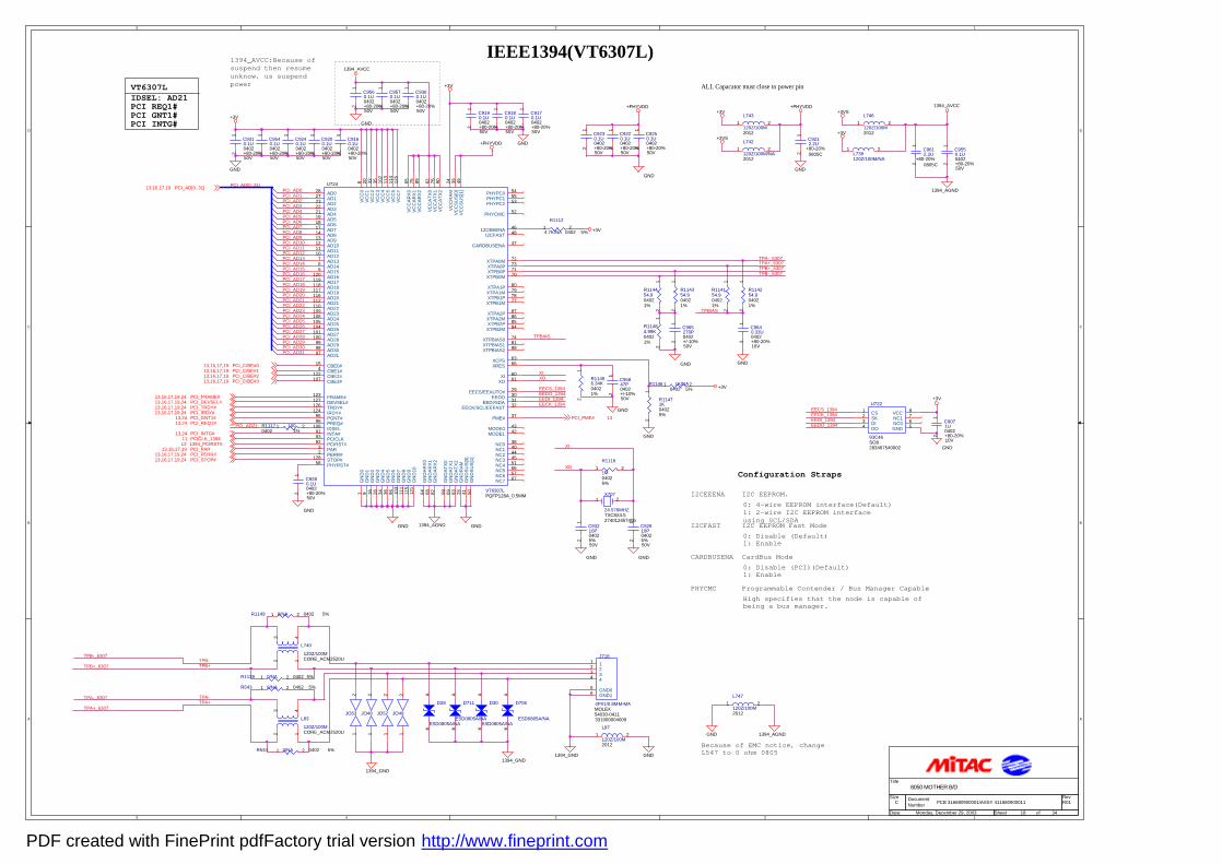
5
5
4
4
3
3
2
2
1
1
D D
C C
B B
A A
IEEE1394(VT6307L)
Configuration Straps
I2CEEENA I2C EEPROM.0: 4-wire EEPROM interface(Default)1: 2-wire I2C EEPROM interfaceusing SCL/SDAI2CFAST I2C EEPROM Fast Mode0: Disable (Default)1: Enable
CARDBUSENA CardBus Mode0: Disable (PCI)(Default)1: Enable
PHYCMC Programmable Contender / Bus Manager CapableHigh specifies that the node is capable ofbeing a bus manager.
VT6307LIDSEL: AD21PCI REQ1#PCI GNT1#PCI INTG#
ALL Capacator must close to power pin
Because of EMC notice, changeL547 to 0 ohm 0805
1394_AVCC:Because ofsuspend then resumeunknow, us suspendpower
PCB 316680900001/ASSY 411680900011 R01
8050 MOTHER B/D
C
18 34Monday, December 29, 2003
Title
Size DocumentNumber
Rev
Date: Sheet of
PCI_AD21
XIXO
XI
EECS_1394EEDO_1394EEDI_1394EECK_1394
EECS_1394EECK_1394EEDI_1394EEDO_1394
TPBIAS
TPBIAS
XO
PCI_AD31
PCI_AD11
PCI_AD14
PCI_AD21
PCI_AD18
PCI_AD15
PCI_AD24
PCI_AD19
PCI_AD5
PCI_AD22
PCI_AD27
PCI_AD8
PCI_AD26
PCI_AD28
PCI_AD30
PCI_AD17
PCI_AD3
PCI_AD9
PCI_AD16
PCI_AD10
PCI_AD7
PCI_AD20
PCI_AD6
PCI_AD0PCI_AD1
PCI_AD29
PCI_AD23
PCI_AD4
PCI_AD13
PCI_AD2
PCI_AD12
PCI_AD25
TPB-_6307
TPA-TPA-_6307
TPA+_6307
TPB-
TPA-_6307
TPB+_6307
TPA+
PCI_AD[0..31]
TPB-_6307
TPB+_6307 TPB+
TPA+_6307
PCI_AD[0..31]13,16,17,19
PCI_C/BE#013,16,17,19PCI_C/BE#113,16,17,19PCI_C/BE#213,16,17,19PCI_C/BE#313,16,17,19
PCI_FRAME#13,16,17,19,24PCI_DEVSEL#13,16,17,19,24PCI_TRDY#13,16,17,19,24PCI_IRDY#13,16,17,19,24PCI_GNT1#13,24PCI_REQ1#13,24
PCI_INTG#13,24PCICLK_139411
PCI_PAR13,16,17,19PCI_PERR#13,16,17,19,24PCI_STOP#13,16,17,19,24
1394_PCIRST#13
PCI_PME# 13
GND
+3V
1394_AVCC
+3V
GND GND
GND
+3V
GND GND
GND
GND
GND
GND
GND
1394_AGNDGND
1394_AGND
+PHYVDD
GND
+3VS+3V
+PHYVDD
1394_AVCC
GND
+PHYVDD
+3V
GND
+3V
GND
1394_GND
1394_GND
+3VS
1394_GND GND
+3V
1394_AGND
R11484.99K04021%
12
R114254.904021%
12
C965270P0402
50V+/-10%
12
C9230.1U0402
50V+80-20%
12
C9310.1U0402
50V+80-20%
12
R1146 1K/NA0402 5%
1 2
L743
120Z/100M2012
1 2
R534 0/NA 0402 5%1 2
D711
ESD0805A/NA
AK
C92910P0402
50V5%
12
JO48
12
D706
ESD0805A/NA
AK
R1117 1000402 1%
1 2
C9212.2U
+80-20%0805C
12
C9570.1U0402
50V+80-20%
12
D28
ESD0805A/NA
AK
C9190.1U0402
50V+80-20%
12
R11471K04025%
12
D30
ESD0805A/NA
AK
C9220.1U0402
50V+80-20%
12
C9540.1U0402
50V+80-20%
12
L83
120Z/100MCORE_ACM2520U1
4
23
U722
93C46SO8283467540002
1234 5
678CS
SKDIDO GND
NC0NC1VCC
C9071U0402
10V+80-20%
12
R1139 0/NA 0402 5%1 2
R1149 0/NA 0402 5%1 2
JO52
12
L87
120Z/100M2012
1 2
L742
120Z/100M/NA2012
1 2
R114354.904021%
12
L739120Z/100M/NA
1 2
JO53
12
C9612.2U
+80-20%0805C
12
C95847P0402
50V+/-10%
12
C9180.1U0402
50V+80-20%
12
C9550.1U0402
50V+80-20%
12
C9250.1U0402
50V+80-20%
12
C9240.1U0402
50V+80-20%
12
L746
120Z/100M2012
1 2
R1116
1M04025%
1 2
R543 0/NA 0402 5%1 2
C9360.1U0402
50V+80-20%
12
C9280.1U0402
50V+80-20%
12
R114154.904021%
12
R11456.34K04021%
12
C9170.1U0402
50V+80-20%
12
C9200.1U0402
50V+80-20%
12
L747
120Z/100M2012
1 2
C9640.33U0402
16V+80-20%
12
J718
4PX1/0.8MM-MAMOLEX54030-0411331000004009
1234
56
1234
GND0GND1
L740
120Z/100MCORE_ACM2520U1
4
23
R1112
4.7K/NA 0402 5%1 2
U724
VT6307LPQFP128A_0.5MM
28272322211918171413121110765
120119118117116112110109106105104101100999897
154
122107
47
127123
1 9 16 26 34 36 94 103
111
115
121
64 68 82 59 69 83 25 41 50
4648
10891
124
9392
95
52
545553
58
96
128
126
3840444551565767
8 20 33 35 102
113
114
125
65 75 89 62 76 90 24 39 49
63
6061
66
748188
7273
7980
8687
7071
7778
8485
32
32
29
3130
4342
37
AD0AD1AD2AD3AD4AD5AD6AD7AD8AD9AD10AD11AD12AD13AD14AD15AD16AD17AD18AD19AD20AD21AD22AD23AD24AD25AD26AD27AD28AD29AD30AD31
CBE0#CBE1#CBE2#CBE3#
CARDBUSENA
DEVSEL#FRAME#
GN
D0
GN
D1
GN
D2
GN
D3
GN
D4
GN
D5
GN
D6
GN
D7
GN
D8
GN
D9
GN
D10
GN
DA
RX
0G
ND
AR
X1
GN
DA
RX
2
GN
DA
TX0
GN
DA
TX1
GN
DA
TX2
GN
DR
AM
GN
DS
US
[0]
GN
DS
US
[1]
12CEEENAI2CFAST
IDSELINTA#
IRDY#
PCICLKPCIRST#
PGNT#
PHYCMC
PHYPC0PHYPC1PHYPC2
PHYRST#
PREQ#
STOP#
TRDY#
NC0NC1NC2NC3NC4NC5NC6NC7
VC
C0
VC
C1
VC
C2
VC
C3
VC
C4
VC
C5
VC
C6
VC
C7
VC
CA
RX
0V
CC
AR
X1
VC
CA
RX
2
VC
CA
TX0
VC
CA
TX1
VC
CA
TX2
VC
CR
AM
VC
CS
US
[0]
VC
CS
US
[1]
XCPS
XIXO
XRES
XTPBIAS0XTPBIAS1XTPBIAS2
XTPA0MXTPA0P
XTPA1MXTPA1P
XTPA2MXTPA2P
XTPB0MXTPB0P
XTPB1MXTPB1P
XTPB2MXTPB2P
PARPERR#
EECK/SCL/EEFAST
EECS/EEAUTO#
EEDI/SDAEEDO
MODE0MODE1
PME#
X707
24.576MHZTXC8X4.5274012457406
1 2
C9160.1U0402
50V+80-20%
12
C9560.1U0402
50V+80-20%
12
C93210P0402
50V5%
12
JO49
12
R114454.904021%
12
PDF created with FinePrint pdfFactory trial version http://www.fineprint.com
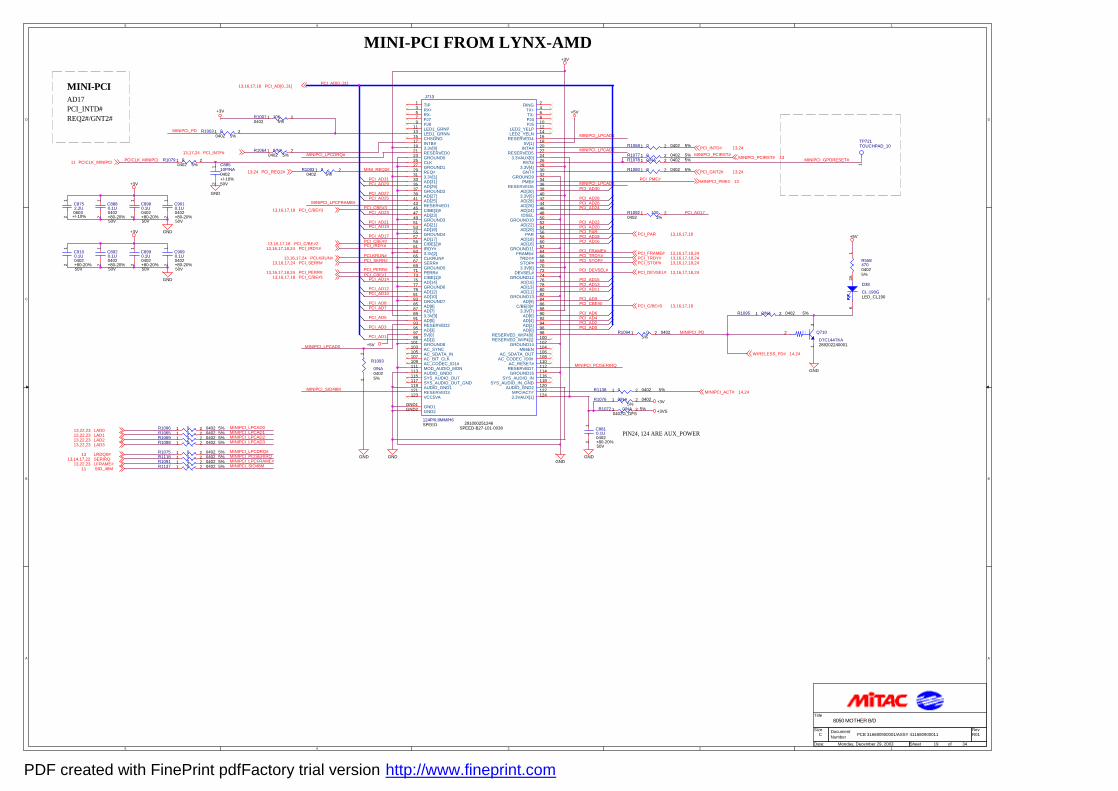
5
5
4
4
3
3
2
2
1
1
D D
C C
B B
A A
MINI-PCI FROM LYNX-AMD
PIN24, 124 ARE AUX_POWER
REQ2#/GNT2#
AD17PCI_INTD#
MINI-PCI
PCB 316680900001/ASSY 411680900011 R01
8050 MOTHER B/D
C
19 34Monday, December 29, 2003
Title
Size DocumentNumber
Rev
Date: Sheet of
PCI_AD[0..31]
MINIPCI_PCIRST#PCICLK_MINIPCI
PCLKRUN#
PCI_CBE#3
PCI_AD20
PCI_AD12
PCI_SERR#
PCI_AD18
PCI_AD10
PCI_CBE#2
PCI_AD23
PCI_STOP#
PCI_PME#
PCI_AD27
PCI_PAR
PCI_AD17
PCI_AD11
PCI_AD16
PCI_AD8
PCI_AD17
PCI_AD15
PCI_AD7
PCI_TRDY#
PCI_AD9
PCI_PERR#
PCI_AD6
PCI_IRDY#
PCI_AD31
PCI_AD2
PCI_AD13
PCI_AD26
PCI_AD5
PCI_AD19PCI_AD21
PCI_AD29
PCI_CBE#0
PCI_AD4
PCI_AD3
PCI_AD24
PCI_AD30
PCI_CBE#1
PCI_AD0
PCI_AD22
PCI_AD1
PCI_AD14
PCI_FRAME#
PCI_AD28PCI_AD25
MINIPCI_PD
PCI_DEVSEL#
MINIPCI_PD
MINIPCI_GPORESET#
MINI_REQ2#
MINIPCI_LPCDRQ#
MINIPCI_LPCAD0
MINIPCI_PCISERIRQ
MINIPCI_LPCFRAME#
MINIPCI_LPCAD1
MINIPCI_LPCAD2
MINIPCI_LPCAD3
MINIPCI_LPCAD3
MINIPCI_LPCAD1MINIPCI_LPCAD0
MINIPCI_LPCAD2
MINIPCI_LPCFRAME#
MINIPCI_LPCDRQ#MINIPCI_PCISERIRQ
MINIPCI_SIO48M
MINIPCI_SIO48M
PCI_AD[0..31]13,16,17,18
PCI_INTF#13,17,24
PCI_PERR#13,16,17,18,24
PCICLK_MINIPCI11
PCI_REQ2#13,24
PCI_C/BE#313,16,17,18
PCI_C/BE#213,16,17,18PCI_IRDY#13,16,17,18,24
PCI_SERR#13,16,17,24
PCI_C/BE#113,16,17,18
PCI_INTD# 13,24
PCI_GNT2# 13,24
PCI_PAR 13,16,17,18
PCI_TRDY# 13,16,17,18,24PCI_FRAME# 13,16,17,18,24
PCI_STOP# 13,16,17,18,24
PCI_DEVSEL# 13,16,17,18,24
PCI_C/BE#0 13,16,17,18
WIRELESS_PD# 14,24
MINIPCI_ACT# 14,24
MINIPCI_PCIRST# 13
MINIPCI_PME# 13
PCLKRUN#13,16,17,24
LAD013,22,23LAD113,22,23LAD213,22,23LAD313,22,23
LFRAME#13,22,23SERIRQ13,14,17,22LRDQ0#13
SIO_48M11
+3V
GND
GND
GND
+3VS
+3V
GND
+5V
GND
+3V
+3V GND
+3V
GND
+5V
GND
+5V
R1095 0/NA 0402 5%1 2
J713
124P/0.8MM/H6SPEED
SPEED-B27-101-0038291000251246
13579
111315171921232527293133353739414345474951535557596163656769717375777981838587899193959799
101103105107109111113115117119121123
2468101214161820222426283032343638404244464850525456586062646668707274767880828486889092949698100102104106108110112114116118120122124
GND1GND2
TIPRX+RX-PJ7PJ8LED1_GRNPLED1_GRNNCHSGNDINTB#3.3V[0]RESERVED0GROUND0CLKGROUND1REQ#3.3V[1]AD[31]AD[29]GROUND2AD[27]AD[25]RESERVED1C/BE[3]#AD[23]GROUND3AD[21]AD[19]GROUND4AD[17]C/BE[2]#IRDY#3.3V[2]CLKRUN#SERR#GROUND5PERR#C/BE[1]#AD[14]GROUND6AD[12]AD[10]GROUND7AD[8]AD[7]3.3V[3]AD[5]RESERVED2AD[3]5V[0]AD[1]GROUND8AC_SYNCAC_SDATA_INAC_BIT_CLKAC_CODEC_ID1#MOD_AUDIO_MONAUDIO_GND0SYS_AUDIO_OUTSYS_AUDIO_OUT_GNDAUDIO_GND1RESERVED3VCC5VA
RINGTX+TX-PJ4PJ5
LED2_YELPLED2_YELN
RESERVED45V[1]
INTA#RESERVED5
3.3VAUX[0]RST#
3.3V[4]GNT#
GROUND9PME#
RESERVED6AD[30]3.3V[5]AD[28]AD[26]AD[24]IDSEL
GROUND10AD[22]AD[20]
PARAD[18]AD[16]
GROUND11FRAME#
TRDY#STOP#3.3V[6]
DEVSEL#GROUND12
AD[15]AD[13]AD[11]
GROUND13AD[9]
C/BE[0]#3.3V[7]
AD[6]AD[4]AD[2]AD[0]
RESERVED_WIP4[0]RESERVED_WIP4[1]
GROUND14M66EN
AC_SDATA_OUTAC_CODEC_ID0#
AC_RESET#RESERVED7GROUND15
SYS_AUDIO_INSYS_AUDIO_IN_GND
AUDIO_GND2MPCIACT#3.3VAUX[1]
GND1GND2
R1091 0 0402 5%1 2
R1079 00402 5%1 2
R1093
0/NA04025%1
2
R1003 00402 5%1 2
R1118 0 0402 5%1 2
TP721TOUCHPAD_10
1
R1092 1000402 1%
1 2
C9100.1U0402
50V+80-20%
12
D38
CL-190GLED_CL190
AK
R1077 0 0402 5%1 2
R1083 00402 5%
1 2
R1078 0/NA 0402 5%1 2
R1064 0/NA0402 5%1 2
R1007 10K0402 5%
1 2
R1065 0 0402 5%1 2R1096 0 0402 5%1 2
C88510P/NA0402
50V+/-10%
12
R1069 0 0402 5%1 2
R1068 0 0402 5%1 2
R1094 0 04025%
1 2
C8920.1U0402
50V+80-20%
12
C9010.1U0402
50V+80-20%
12
C8990.1U0402
50V+80-20%
12
R1080 0 0402 5%1 2
R1075 0 0402 5%1 2
R1088 0 0402 5%1 2
R1072 0/NA 5%0402G_DFS1 2
R1137 0 0402 5%1 2
C8752.2U0603+/-10%
12
R1076 0/NA 04025%
1 2
C8880.1U0402
50V+80-20%
12
R1138 0 0402 5%1 2
R1 Q710
DTC144TKA288202240001
2
13
C9090.1U0402
50V+80-20%
12
C8810.1U0402
50V+80-20%
12
R55847004025%
12
C8980.1U0402
50V+80-20%
12
PDF created with FinePrint pdfFactory trial version http://www.fineprint.com
5
5
4
4
3
3
2
2
1
1
D D
C C
B B
A A
20mil
L.CH
R.CH
273000130006
JP, use 4pcs of 2kV 1000P cap
UK, use 4pcs of 3kV 1000P cap
GND_45
US, use 2pcs of 2kV 1000P capCLOSE TO MDC
AUDIO CODEC(ALC655)
MDC
FOR EMI REQUEST CHANGE TO 0 OHM
PCB 316680900001/ASSY 411680900011 R01
8050 MOTHER B/D
C
20 34Monday, December 29, 2003
Title
Size DocumentNumber
Rev
Date: Sheet of
MIC2ACSYNC
CDROM_RIGHT
ACRST#
CDROM_COMM
ACSDOUTMIC1
ACSDIN0
AOUT_R
CDROM_LEFT
PC_BEEP
ACBITCLK
JD0
MONO_OUT
AOUT_L
MODEM_SPK
AVDD
MIC
MIC_VREF
2464_VREF
MIC_INT
LINE_IN/L
LINE_IN/R
AOUT_R
SUB_OUTL
SUB_OUTR
AOUT_L
SBSPKR
CARDSPK# PC_BEEP
LINE_IN/L
LINE_IN/R
MODEMN
ACBITCLK
ACSDOUT
ACBITCLK
ACSDIN1
MODEM_SPK
ACSYNC
ACRST#
MONO_OUT
MODEMP
MIC_VREF MIC_EXT
ACRST#14ACSDOUT14ACSDIN014ACSYNC14ACBITCLK14
EAPD21
14M_CODEC11
CDROM_RIGHT 15
CDROM_LEFT 15
CDROM_COMM 15
2464_VREF 21
AMP_RIGHT 21
AMP_LEFT 21
SUB_OUTL21
SUB_OUTR21
SUB_RIGHT 21SUB_LEFT 21
CARDSPK#17
SBSPKR13,14
MODEMP 16MODEMN 16
ACSDIN1 14
SPDIFOUT21
GND
AGND
AGND AGND
GND
AGND
AGND
GND
GND
AGND
AGND
+3V
GND
AGND
AGND
AGND
GND
GND
AGND
+5VVA
AGND
CAGND
AGND
AGND
AGND AGNDAGND AGND
AGND
AGND
GND
AGND
AGND
GND
AGND
GND
GND
AGND
CAGND
CAGND
CAGND
AGND
GND
GND
VA
AGND
AGND
CAGND
CAGND
GND
GND
AGND
AGND
GND
+3VS
GND GND
+3V
+3V
GND
+5V
GND
AGND
AGND
CAGND
GND
L72450UHCHOKE_WLT04020201
21
35
R52022K04021%
12
C962 1000P0402 50V 10%
1 2
R5496.8K04025%
12C959 1U
0402 10V +80-20%1 2
L64120Z/100M/NA
201212
R5376.8K04025%
12
C975 1U0402 10V +80-20%
1 2
C5180.1U/NA0402
16V10%
12
R1155 00603
1 2
L62
120Z/100M2012
1 2
C9720.1U/NA0402
50V+80-20%
12
J10
12
C953 1U0402 10V +80-20%
1 2
C948100P/NA0402
50V+/-10%
12
R5190 04025%
1 2
C460 0.1U
0402 16V
10%
1 2
L725120Z/100M/NA
201212
J715
HDR/MA-2ACES85204-0200291000020206
12
R11361K04025%
12
R535 00402 5%
1 2
C47510U
10V1210
12
R11340/NA 0402 5%
1 2
L66120Z/100M
2012
12C455
100P0402
50V+/-10%
12
L57BEAD_600Z/100M
0603D1 2
C9661U0402
10V+80-20%
12
C974 1U0402 10V +80-20%
1 2
R1123 0/NA0402 5%
12
R112927K/NA04025%
12
R503 0/NA0402 5%
1 2
R324
0 04025%1 2
C4810.1U0402
16V10%
12
C976 1U0402 10V +80-20%
1 2
R547 6.8K 0402 5%1 2
C91210P/NA0402
50V+/-10%
12
R32522K04021%
12
X2
24.576MHZ/NATXC8X4.5
274012457406
1 2
R1153
0 04025%
1 2
R1127 4.42K0402 5%
1 2
R849560-2010/NA
0805
12
C515 0.22U0402 16V +80-20%
1 2
L76
BEAD_600Z/100M
0603D1 2
R1151
4.7/NA0402 5%1 2
C9130.1U0402
10V10%
12
C960 1000P0402 50V 10%
1 2
C507 1U0402 10V +80-20%
1 2
R1130 4.42K0402 5%
1 2
C969 1U0402 10V +80-20%
1 2
R44247K04025%
12
C5010.1U0402
16V10%
12
R484180K/NA06031%
12
R1124 00402 5%
12
L721120Z/100M/NA
201212
J11
12
R472 00402 5%
1 2
R1120 22 04025%1 2
L53BEAD_600Z/100M
0603D1 2
C970 1U0402 10V +80-20%
1 2R530 220402 5%
1 2
C940 1U0402 10V+80-20%
1 2
C94247P/NA0402
50V+/-10%
12
C939 1U0402 10V+80-20%
1 2
C47622P/NA0402
50V+/-10%
12
C9260.1U0402
10V10%
12
C5092200P0402
50V+/-20%
12
C9380.1U0402
50V+80-20%
12
R1154
4.7K04025%
1 2
R11330/NA04025%
12
R1135 00402 5%
1 2
C4670.01U0402
50V+80-20%
12
C980 1U/NA0402 10V +80-20%
1 2
D718
ESD0805A/NA0603B_0805C
1 2
L734BEAD_600Z/100M
0603D1 2
C9680.1U0402
50V+80-20%
12
C9270.1U0402
10V10%
12
C9631U0402
10V+80-20%
12
C516 1U0402 10V +80-20%
1 2
R1157
0 04025%1 2
R1131 22 04025%1 2
C50422P/NA0402
50V+/-10%
12
C4570.1U040216V10%
1 2
R1121 22/NA 04025%1 2
R112627K/NA04025%
12
U18
MIC5205BM5SOT25
1234
5 INGND
ENADJ
OUT
C952 1U/NA0402 10V +80-20%
1 2
U726
ALC655PQFP48_0.5MM
2
3
5
6
810
11
17
16
45464748
27
28
31
12
13
14
15
18
19
20
21
22
23
24
34
32 35
36
37
39
41
4344
29
30
33
4026 424 7
25 381 9
XTL-IN
XTL-OUT
SDATA-OUT
BIT-CLK
SDATA-INSYNC
RESET#
JD1/GPIO1
JD2
JD0/GPIO0XTLSELSPDIFI/EAPDSPDIFO
VREF
VREFOUT
VRDA
PC-BEEP
PHONE
AUX-L
AUX-R
CD-L
CD-GND
CD-R
MIC1
MIC2
LINE-L
LINE-R
FRONT-MIC1
FRONT-MIC2 LINE-OUT-L
LINE-OUT-R
MONO-OUT
S-OUT-L
S-OUT-R
CEN-OUTLFE-OUT
AFILT1
AFILT2
NC_0
NC_1A
VS
S1
AV
SS
2
DV
SS
1D
VS
S2
AV
DD
1A
VD
D2
DV
DD
1D
VD
D2
R1150 00603
1 2
R538 6.8K 0402 5%1 2
C4580.1U040216V10%
1 2
R5466.8K04025%
12
R438
10K04025%
1 2
L741
120Z/100M/NACORE_ACM2520U
14
23
C330100P0402
50V+/-10%
12
U17
NC7S32SOT25
123
54A
BGND
VCCY
R4371K04025%
12
C937 0.1U0402 16V 10%
1 2
R497 0/NA0402 5%
1 2
C498100P0402
50V+/-10%
12
R498 220402 5%
1 2
L70BEAD_600Z/100M
0603D1 2
D705ESD0805A/NA0603B_0805C
12
R516
1M/NA 0402
1 2
R532 00402 5%
1 2
C148 1000P 2KV10%18081 2
R559 10K/NA0402 5%
1 2
R550 0 0402 5%1 2
C9331000P/NA0402
50V10%
12
JO724
SPARKGAP_6
12
C159100P/NA0402
50V+/-10%
12
R116422K/NA 0402 1%1 2
C519 0.1U/NA0402 16V 10%
1 2
L751
120Z/100M1608
12J717
FM/0.8MM/H2.4AMP C-179373
291000023008
13579
11131517192123252729
24681012141618202224262830
R452470K/NA04025%
12
C456
1U040210V+80-20%
1 2
R1128 00402 5%
1 2
+-
MIC1
D5.8/H2.0EM147TK339115000046
12
R1132
4.7K
0402
5%1 2
C49110U
6.3V0805
10%
12
C47722P/NA0402
50V+/-10%
12
L744
BEAD_600Z/100M0603D
12
C9710.1U/NA0402
50V+80-20%
12
C9670.1U0402
16V10%
12
C945 0.1U/NA0402 16V 10%
1 2
C499100P/NA0402
50V+/-10%
12
L65
120Z/100M2012
1 2
L88
120Z/100M2012
1 2
R5601K/NA04025%
12
JO725
SPARKGAP_6
12
L73
120Z/100M2012
1 2
F2
MINISMDC014-2POLYSW_MINISMDC110
1 2
J719
RA/D6/6P2SJ-SB2014D3CONN_JACK_SB2014291000920605
1
62
345
L69 0 16081 2
C806 1000P 2KV 10%18081 2
R44347K04025%
12
C9734.7U/NA
6.3V0603
+80-20%
12
C513 1U0402 10V +80-20%
1 2
C979 1U/NA0402 10V +80-20%
1 2
R5425.6K04025%
12
J721
RA/D6/6P2SJ-SB2014D3CONN_JACK_SB2014291000920605
1
62
345
PDF created with FinePrint pdfFactory trial version http://www.fineprint.com
5
5
4
4
3
3
2
2
1
1
D D
C C
B B
A A
USE 3K 1%
USE 2200P10%
USE 2200P10%
USE 3K 1%
SUBWOOFER AMP(LM4871)
AUDIO AMPLIFIER
on device
0
OPT in0
HP in
1
REMARK
1
0
no this condition
0
DEVICE_DECT#
1
DECT_HP#/OPT
1
PCB 316680900001/ASSY 411680900011 R01
8050 MOTHER B/D
C
21 34Monday, December 29, 2003
Title
Size DocumentNumber
Rev
Date: Sheet of
SUB_OUTR
SUB_OUTL
2464VREF1
2464VREF2
SUB_OUTR
SUB_OUTL
SUB_OUTL
SUB_OUTRRIN_2464
2464VREF1
SUB_RIGHT
2464VREF2
SUB_LEFT SUB_OUTL
SUB_OUTR
ROUT+
AMPVDD
AMP_RIGHT
SPK_OFF#
AMPVDD
AMP_LEFT
AMP_OFF
AMP_SHUTDOWN
ROUT-
DEVICE_DECT#AGND
DECT_HP#OPT
DECT_HP#OPT
DEVICE_DECT#
DEVICE_DECT#
DEVICE_DECT
DEVICE_DECT
AMP_SHUTDOWN
OPTIN#
OPTIN#
SPK_OFF#
AMPVDD
AMP_OFF
SUB_LEFT20
SUB_RIGHT20
2464_VREF20
SUB_OUTL 20
SUB_OUTR 20
AMP_LEFT20
AMP_RIGHT20
EAPD20
SPK_OFF13,24
SPDIFOUT20
KBC_MUTE22
AGND GND
+5V
GND
AGND AGND
AGND
VA
VA
AGND
VA
AGND
AGND
AGND
AGND
AGND
AGND
AGND
AGND
AGND AGND
CAGND
AGND
AGND
+5V
AGND
AGND
GND
GND
+5V+3V
+5V
+5VS_SUBAMP
AGND
AGND
AGND
AGND
AGND
VA
AGND
GND
+3V
AGND
VA
+5V
GND
CAGNDCAGND
GND
CAGND
CAGND
AGND
R118310K0402
12
L758600Z/100M1608
12
DS
Q362N7002/NA
G
DS
C490
0.15U0603
1 2
R4541K04025%
12
R1 Q52
DTC144TKA288202240001
2
13
JO101 2
R329 22 0402 5%12
R461
3K/NA0402 5%
1 2
+ C489
100U6.3V20%
12
C496 0.22U
0402 16V+80-20%1 2
R1 Q23
DTC144TKA288202240001
2
13
D6
ESD0603/NA
12
C483 0.22U
0402 16V+80-20%1 2
R463
22.1K 0402 1%
1 2
R1161 100K 0402 5%1 2
C4702200P0402
50V+/-20%
12
R391 100K/NA 0402 5%1 2
D27
RLS4148
A K
R1160 100K/NA 0402 5%1 2
D22
BAT54C
1
23
L63
120Z/100M2012
1 2
R510
22.1K 0402 1%
1 2
C493 1U0402 10V
1 2
L52600Z/100M 16081 2
D19
RLS4148
A K
L757600Z/100M
16081 2
R451 10K/NA04025% 12
C492 1U0402 10V +80-20%
1 2
C484 1U0402 10V
1 2
+ C951
100U6.3V20%
12
C356100P/NA0402
50V10%
12
R46047K/NA04025%
12
+ C474
100U6.3V20%
12
J3
HDR/MA-2ACES85204-0200291000020206
12
L50600Z/100M 16081 2
R509
22.1K 0402 1%
1 2
R50718K04021%
12
R506
3K/NA0402 5%
1 2
L759600Z/100M1608
12
R4891M/NA04025%
12
C485 1U0402 10V +80-20%
1 2
R3224.7K04025%
12
L80 600Z/100M 16081 2
R491 0/NA 0402 5%1 2
D5
ESD0603/NA
12
R26 0 08051 2R27 0 08051 2
R1302 00402
1 2
R1122 22.1K0603 1%
1 2
C354100P/NA0402
50V10%
12
C487
1U/NA10V0805
1 2R521 00402
1 2
C9414.7U
0805+80-20%
12
C9771U040210V
12
U524
TPA0212_GNDTSSOP24_TPA0102
23
4
56
78
910
11
14
15
16
17
18
19
20 21
22
23
1121324
2526272829
3031323334
GAIN0GAIN1
LOUT+
LLINEINLHPIN
PVDD0RIN
LOUT-LIN
BYPASS
PC-BEEP
SEBTL
ROUT-
HP/LINE
PVDD1
VDD
RHPIN ROUT+
SHUTDOWN
RLINEIN
GND0GND1GND2GND3
G1G2G3G4G5
G6G7G8G9G10
R4711M/NA04025%
12
C4942200P0402
50V+/-20%
12
R5291K04021%
12
R511 100 04021%
1 2
R1Q30
DTC144TKA/NA
2
13
R118510K0402
12
C9340.1U0402
16V10%
12
L14 600Z/100M 16081 2
C9490.1U0402
16V10%
12
C9301U0402
10V+80-20%
12
C4620.1U/NA0402
50V+80-20%
12
C935 1U0402 10V +80-20%
12
R512 0/NA 0402 5%1 2C482
0.15U0603
1 2
DS
Q352N7002/NA
G
DS
C150100P0402
50V10%
12
L55600Z/100M
16081 2
C1003100P/NA0402
50V+/-10%
12
L755600Z/100M
16081 2
D715
BAW56288100056017
2
13
C3451U/NA0402
10V+80-20%
12
C4690.1U0402
50V+80-20%
12
R11581.3M04021%
12
C500
10U6.3V080510%
12
L16 600Z/100M 16081 2
C480 1U0402 10V
1 2
TP491
J705
HDR/MA-2ACES85204-0200291000020206
12
L67
120Z/100M 20121 2
LEDDriveIC
J720
GP1FD310TPSHARPCONN_GP1FD310TP
54231
879
L754600Z/100M
16081 2
R496 10.2K0402 1%
1 2
R1125 00402
1 2
+
-U19ALMV822MSOP8
3
21
84
C497 1U0402 10V +80-20%
1 2
R478 00402
1 2
J7
HDR/MA-2ACES85204-0200291000020206
12
R528 22 0402 5%12
R477100K04025%
12
R1
Q38
DTC144TKA288202240001
2
1 3
Q711
DTA144WKSOT23AN_1
288221371002
1
2
3
U725
LM4871LLP8A
34
58
217 69
101112
131415
+IN-IN
VO1VO2
BYPASSSHDWNGND VDDGND1GND2GND3GND4
GND5GND6GND7
L78 600Z/100M 16081 2
C4711000P
060310%
1 2
L752
120Z/100M 20121 2
C950 1U0402 10V +80-20%
12
R12394.7K04025%
12
C978
1U/NA040210V+80-20%
12
R46218K04021%
12
C479
1U/NA10V0805
1 2
C503100P0402
50V10%
12
+
-U19BLMV822MSOP8
5
67
84
R459 10K/NA04025% 12
R1159 100K 0402 5%1 2
R3281K04021%
12
R36710K0402
12
R1
Q713DTC144TKA2882022400012
13
+ C466
100U6.3V20%
12
JO121 2
R479
22.1K 0402 1%
1 2
R502 10.2K0402 1%
1 2
D17
RLS4148
A K
PDF created with FinePrint pdfFactory trial version http://www.fineprint.com
5
5
4
4
3
3
2
2
1
1
D D
C C
B B
A A
For Externalflash
10MIL
1:external flash0:internal flash
20MIL Pull HIGH at Other End
X7R
3V LEVEL
WINBOND KBC PULL HIGH at SB END
0:for external flash
POWER BUTTON
ADD-->R0B
Closed to KB CONN
R0AaddC Version 284583950002
KBC IC :284583950002F/WASSY:481677700002
Processor Hot Protection
THERMAL SENSOR / FAN CONTROLLER
FAN
PCB 316680900001/ASSY 411680900011 R01
8050 MOTHER B/D
C
22 34Monday, December 29, 2003
Title
Size DocumentNumber
Rev
Date: Sheet of
KI4
KI7
KI0KI1
KO5KO6
KI5
KO14
KO0
KI3
KO1KO0
KI0
KO3
KO1
KI7
KI1
KO12
KI2
KO4
KI7
KI1
KO12
KO15
KO8
KI3
KO11
KO14
KO7
KO2
KI6
KO9KO9
KO2
KI5KI4
KO15
KO8
KO11KO10
KO6
KO4
KO13
KI3KI2KI5
KI6
A20GATE
BAT_DATABAT_CLK
H8_HRCIN#
T_CLKT_DATA
H8_RSMRST
BAT_DATA
BAT_CLKH8_THRM_CLK
H8_I_LIMITI_LIMIT
H8_SCI
H8_I_CTRI_CTRL
H8_THRM#
KI5
H8_ENABKL
KI4
KO7
H8_I_LIMIT
T_DATA
KBC_X+KO11
KO4
BAT_DATA
AC_POWER#
LAD2
NUM#
KO15
KO2
LAD1
H8_THRM#
KO13
LAD3
KO6
KI1
KO12
BLADJ
KO3
KI7
LAD0
CAP#
KO14
H8_I_CTR
H8_ADEN#
BLADJ
PWRBTN#
KBC_X-
KI5
KO5
H8_RSMRST
EXTSMI#
SCROLL#
KBC_X-
KI3
BAT_CLK
ICH_PWRBTN
H8_PWRON
BATT_R#
H8_ENABKL
BAT_TEMP
KI6
KO10
KO0
BATT_G#
H8_RESET#
KI0
BAT_VOLT
H8_SCI
PWRBTN#
KI2
KO1
SW_VDD3
KBC_X+
KO9KO8
T_CLKBATT_DEAD#
H8_WAKE_UP#H8_SUSB
CHARGING
KBC_RI#
H8_PROCHOT#
H8_RSMRST
H8_ADEN#
H8_SUSBICH_PWRBTN
H8_SUSB
PWRBTN#
BATT_DEAD#
H8_PROCHOT# HPROCHOT#
H8_PROCHOT#
BAT_CLK
BAT_DATA
BAT_DATA
LAD[0..3]
LEARNING
FAN_SPEED
H8_THRM_DATA
FAN#
THERM_ERR#
H8_THRM_CLK
ICH_PWRBTN
BATT_DEAD#
H8_THRM_DATA
BAT_CLK
FAN_SPEED
FAN#
KBC_RI#
H8_SCI
H8_WAKE_UP#WAKE_UP#
H8_THRM#
H8_HRCIN#
KI0
KI2
KO10
KO3
KO5
KO7
KO13
KI6
KI4
LAD[0..3]13,19,23
PCICLK_KBC11SERIRQ13,14,17,19
KBC_PCIRST#13LFRAME#13,19,23
ADEN#25,32LEARNING32
SUSB# 13,17,23,25
SCI#13,24
BAT_D 32BAT_C 32BAT_T 32BAT_V 32
SUSC# 13,26,27
CHARGING33
H8_LIDSW# 12
H8_ENABKL12
T_CLK 23
T_DATA 23
A20GATE 13
BLADJ4,12I_CTRL33I_LIMIT32
KBD_US/JP# 13,24
BATT_R# 12,23
NUM# 23
BATT_G# 12,23
CAP# 23
SCROLL# 23
ICH_PWRBTN#13
BATT_DEAD33
EXTSMI# 13,24
SB_THRM#13
SW_VDD325
CPU_THERMDC 2
CPU_THERMDA 2
VGA_THERMDA 9
VGA_THERMDC 9
HPROCHOT# 2
H8_PWRON 26,27
RSMRST# 13,25
BATT_LED#23KBC_PWRON_VDD3S25
AC_POWER# 12,23
H8_PWRON_SUSB# 25
THERM_ERR#14,25
H8_RESET# 25
KBC_RI# 16
WAKE_UP#13,24
HRCIN#13
KBC_MUTE 21
GND
GND
GND
GND
GNDGND
GND
H8AGNDH8AGND
VDD3
VDD3
VDD3
+KBC_CPUCORE
GND
+VCC_CORE
VDD3 VDD3_AVREF
+5V
GND
GND
+5VS +5VS
GND GND
+3V
GND
VDD3
GND
VDD3
VDD3_AVREF
+VCC_CORE
+3VS
VDD3
VDD5
+2.5VS_DDR
+3VS
+3VS
GND
+KBC_CPUCORE
GND
VDD3S
GND
GND+3VS
VDD3_AVREF
VDD3
+5V
GND
GND
+3V
GND
GND
+3VS
+3V
VDD3
GNDH8AGND
+3V +3V
+3V
R1
Q706
DTC144TKASOT23AN_1288202240001
2
13
R92510K0402
12
RP719
10K*4 1206
1234
8765
R993304025%
1 2
C7282200P0402
50V+/-20%
12
R450 10K/NA0402
12
C4530.1U0402
50V+80-20%
12
R475 10K0402 5%
1 2
R1 Q39
DTC144TKASOT23AN_1288202240001
2
13
R1Q32
DTC144TKASOT23AN_1
288202240001
2
13
R413 10K 04025% 12
C534100P
040250V
1 2
C91000P0402
50V+/-20%
12
C524100P
040250V
1 2
RP45
22*4RPSOA_8C
1234
8765
C538100P
040250V
1 2
R39510K0402
12
C537100P
040250V
1 2
R453
10K04025%
12
R455 2.7K/NA 04021%1 2
U706
ADT7460QSOP16B
11
1
2
16
3
4
15
10
14
6
513
8
7
12
9
D2+
SCL
GND
SDA
VCC
TACH3
PWM1
D2-
+2.5VIN/SMBALERT
TACH1
PWM2/SMBALERTD1+
PWM3/ADDRESS ENABLE
TACH2
D1-
TACH4/ADDRESS SELECT/THERM
C4490.1U0402
50V+80-20%
12
DS
Q40
2N7002G
DS
D21 RLS4148AK
C45022P0402
50V+/-10%
12
D703
RLS4148
A K
C527100P
040250V
1 2
R9510K04025%
12
C1330.1U0402
50V+80-20%
12
C4540.1U0402
50V+80-20%
12
C940.1U0402
50V+80-20%
12
R439 00402
1 2
R1
Q27
DTC144TKASOT23AN_1288202240001
2
13
R482 10K 04025% 12
R449 2.7K 04021%1 2
C526100P
040250V
1 2
R448 2.7K 04021%1 2
C540100P
040250V
1 2
R481 10K 04025% 12
SW2
TC010-PSS11CET297004010001
13
245
D20RLS4148/NAAK
R445 00402
1 2
C1040.1U0402
50V+80-20%
12
R473 00402
1 2
R385 0/NA0402 5%
1 2
C539100P
040250V
1 2
C4480.1U0402
50V+80-20%
12
C4780.1U0402
50V+80-20%
12
TP719 1
L61
120Z/100M/NA0805C
1 2
C4590.1U0402
50V+80-20%
12
C44510U
6.3V0805
10%
12
R428 0 04021 2
R414 0/NA 5%0402G_DFS1 2
C529100P
040250V
1 2C528100P
040250V
1 2
R4041M
0402 5%1 2
C542100P
040250V
1 2
R425 10K/NA0402 5%
1 2
TP720 1
D18BAV70LT1SOT23N2881000700061 2
3
R486 00402
1 2
R447
0/NA04025%1
2
DS G
Q14SI2301DS
G
DS
R7 1K0402 5%
1 2
R390 10K/NA0402 5%
1 2
DS
Q33
2N7002G
DS
C8692200P0402
50V+/-20%
12
J707
1.25MM/ST/MA-3ACES85205-0300291000010303
123
DS
Q42FDV301NSOT23_FET
G
DS
R1Q49
DTC144TKASOT23AN_1
288202240001
2
13
C541100P
040250V
1 2
TP718 1
R381 0/NA0402 5%
1 2
R1002
0
12
RP46
RP10KX8RPSOE_10
123456
789
10
C530100P
040250V
1 2C531100P
040250V
1 2
C523100P
040250V
1 2
C8714.7U0805+80-20%
12
R483 0 04021 2
R87004025%
1 2
R394 0/NA0402
1 2
RP44
4.7K*81206
123456
789
10
C9310U16V1206
12
L68BEAD_600Z/100M
0603D1 2
C44722P0402
50V+/-10%
12
C522100P
040250V
1 2
C520100P
040250V
1 2
U16
W83L950D
PQFP80_0.5MM
3132333435363738
1
20
7069686766656463
171514232219
21
1618
987654
55
1110
80797877767574
32
2726
1312
54535251504948474645444342414039
62616059585756
24
25
28
29
30
71
72
73
GP27/FD7GP26/FD6GP25/FD5GP24/FD4
GP23/FD3/SCL1/TXD1GP22/FD2/SDA1/RXD1
GP21/FD1GP20/FD0/LPCEN
GP60/AN0/INT5
GP45/TXD
GP80/SD0GP81/SD1GP82/SD2GP83/SD3GP84/SD4GP85/SD5GP86/SD6GP87/SD7
GP50/A0GP52/INT30#/RGP53/INT40#/WGP42/INT0/OBF00GP43/INT1/OBF01GP46/SCLK1/OBF1
GP44/RXD
GP51/INT20#/S0GP47/SRDY1#/S1
GP70/SIN2P71/SOUT2
GP72/SCLK2GP73/SRDY2#/INT21
GP74/INT31GP75/INT41
GP37/OE#
GP56/DA1/PWM01GP57/DA2/PWM11
GP61/AN1/INT6GP62/AN2/INT7GP63/AN3/INT8GP64/AN4/INT9
GP65/AN5/INT10GP66/AN6/INT11GP67/AN7/INT12
GP76/SDAGP77/SCL
GP40/XOUT/PWM2GP41/XCIN/PWM3
GP54/CNTR0GP55/CNTR1
GP0/P3REF/FA0GP1/FA1GP2/FA2GP3/FA3GP4/FA4GP5/FA5GP6/FA6GP7/FA7GP10/FA8GP11/FA9GP12/FA10GP13/FA11GP14/FA12GP15/FA13GP16/FA14GP17/FA15
GP30/PWM0/FCTRL0GP31/PWM10/FCTRL1GP32/FCTRL2GP33/FCTRL3#GP34/BANK0GP35/BANK1GP36/CE#
CNVSS
RESET#
XIN
XOUT
VSS
VCC
VREF
AVSS R419 2.7K/NA 04021%1 2
R424 220402 5%
1 2
R961M/NA04025%
12
C543100P
040250V
1 2
C521100P
040250V
1 2
R8810K04025%
12
C532100P
040250V
1 2
R393 00402
1 2
R44615004021%
12
X1
8MHZTXC8X4.5
1 2
C536100P
040250V
1 2C535100P
040250V
1 2
C533100P
040250V
1 2
R1
Q26DTC144TKASOT23AN_1288202240001
2
13
R1Q31
DTC144TKASOT23AN_1
288202240001
2
13
J5
FPC/FFC/1MM/26PACES85202-26-00291000152603
1234567891011121314151617181920212223242526
R1
Q29
DTC144TKA288202240001
2
13
R267 0/NA0402 5%
1 2
C525100P
040250V
1 2
R430
10K04025%1
2
PDF created with FinePrint pdfFactory trial version http://www.fineprint.com
5
5
4
4
3
3
2
2
1
1
D D
C C
B B
A A
TOUCH_PAD
SW_RIGHT
SW_LEFT
miniSMDC050
LED
FWH
SYS BIOS Vendor List:
SST49LF004A : 283467490001
When 8050N ADD J722 and DEL J4When 8050 ADD J4 and DEL J722
PCB 316680900001/ASSY 411680900011 R01
8050 MOTHER B/D
C
23 34Monday, December 29, 2003
Title
Size DocumentNumber
Rev
Date: Sheet of
TP_RIGHT
TP_LEFT
TP_CLK
AC_BATT_LED#
NUM#
SCROLL#
LAD2
LAD0
INIT#
LAD1
TP_DATATP_VDD
LAD3INIT#
CAP#
AC_BATT_LED# IDE_LED#
IDE_LED#
BATT_POWER#
BATT_LED#
TP_DATA
TP_RIGHT
TP_VDD
TP_LEFT
TP_CLK
SUSB#13,17,22,25
HDD_LED#15
CD_LED#15
SCROLL#22
CAP#22
NUM#22
BATT_LED#22
PCICLK_FWH11
LFRAME# 13,19,22
FWH_PCIRST#13
LAD113,19,22LAD013,19,22
LAD313,19,22LAD213,19,22
T_CLK22
T_DATA22
HINIT#2,13
CAP#22
NUM#22
CD_LED#15
HDD_LED#15
BATT_G#12,22
BATT_POWER#12
AC_POWER#12,22
BATT_R#12,22
GND
GND
+5V
GND
GND
+3VS+3VS +3VS
GNDGND GND
+3V
+5V
+5V
GND
GND
+3V
GND
+3V
GND
GND
GND
GND GND
GND
+3V
GND
+5V
VDD3S
VDD3S
VDD3S
GND
R422 8.2K 04025%1 2
D37CL-190G
AK
R415
0/NA04021 2
R427 8.2K 04025%1 2
J8
HDR/MA-12/NAACES87151-1207291000141204
123456789
101112
D23
ESD0805A/NA
1 2
R364 4.7K 04025%
1 2
R554470
0402 5%1 2
C14447P0402
50V+/-10%
12
R4320/NA
04021 2
R4580
04021 2
R429
004021 2
R1 Q719DTC114TKA
288202215001
2
13
U703C
74AHC14_VTSSOP14
56
147
R1303
0/NA04021 2
R433220/NA
04025%
1 2
U703B
74AHC14_VTSSOP14
34
147
R468
004021 2
R556220
0402 5%1 2
JO19
12
R434220/NA
04025%
1 2
C14347P0402
50V+/-10%
12
R151 0/NA 5%0402G_DFS1 2
F701
0.5A/POLYSW
1 2
R1073
33004025%
1 2
R420
004021 2
JO181
2JO20
12
R417 4.7K 04025%1 2
JO21
12
R132 0/NA 5%0402G_DFS1 2
R441
470/NA0402 5%1 2
D35CL-190G
AK
Q708MMBT3904L288203904022
B
EC
R4260/NA
04021 2
R555
2200402 5%1 2
C9020.1U0402
10V10%
12
C15447P0402
50V+/-10%
12
R402 8.2K 04025%1 2
R1
Q720DTC114TKA288202215001
2
13
D33CL-190G
AK
R1140 180K 0402 5%1 2
R4160
04021 2
C771 0.1U
040250V +80-20%
1 2
L716
120Z/100M2012
12
L36120Z/100M1608
1 2
R4650/NA
04021 2
R4660/NA
04021 2
R1089
33004025%1
2
D32CL-190G
AK
R411 8.2K 04025%1 2 C8970.1U0402
10V10%
12
TP56 1
C17247P0402
50V+/-10%
12
U703D
74AHC14_VTSSOP14
98
147
U15
SST49LF004A
4 3
56789
10111213
14 15 16 17 18 19 20
212223242526272829
2 1 32 31 30
A8/
RS
VA
9/R
SV
A7/RSVA6/RSVA5/RSVA4/RSVA3/RSVA2/RSVA1/RSVA0/RSVLAD0/DQ0
DQ
1/LA
D1
DQ
2/LA
D2
GN
DD
Q3/
LAD
3D
Q4/
RS
VD
Q5/
RS
VD
Q6/
RS
V
DQ7/RSVNC
WE#/LFRAME#OE#/INIT#
VDDGND
VCCAGNDAMODE
RE
SE
T#V
PP
VD
DR
-C#/
CLK
A10
/GP
I4
R423 8.2K 04025%1 2
R408 4.7K 04025%1 2
D721
BAW56/NA
2
13
D34CL-190G
AK
R418 8.2K 04025%1 2
D29
ESD0805A/NA
1 2
R457
0/NA04021 2
R557220
0402 5%1 2
R553470
0402 5%1 2
R412 8.2K 04025%1 2
Q718MMBT3904L288203904022
B
EC
J4
HDR/MA-6ACES87151-0607
123456
C9474.7U0805+80-20%
12
C9084.7U
6.3V0603
+80-20%
12
R1152 1M04025%
1 2
SW4
TC010-PSS11CET297004010001
13
245
R403 8.2K 04025%1 2
R467220/NA
0402 5%1 2
SW5
TC010-PSS11CET297004010001
13
245
TP57 1
VG
SR
D31
19-22SRVGC/TR8/NA
34
12
L37120Z/100M1608
1 2
R387 8.2K 04025%1 2
R10841.5K04025%
12
R421
004021 2
PDF created with FinePrint pdfFactory trial version http://www.fineprint.com
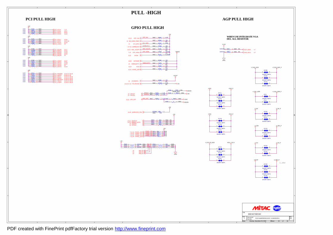
5
5
4
4
3
3
2
2
1
1
D D
C C
B B
A A
PULL -HIGH
1.05V
AGP PULL HIGHPCI PULL HIGH
GPIO PULL HIGH
WHEN USE INTEGRATE VGADEL ALL RESISTOR
PCB 316680900001/ASSY 411680900011 R01
8050 MOTHER B/D
C
24 34Monday, December 29, 2003
Title
Size DocumentNumber
Rev
Date: Sheet of
MB_ID0MB_ID1MB_ID2
PANEL_ID1PANEL_ID0
PANEL_ID3PANEL_ID2
KBD_US/JP#
SMBALERT#
AGPBUSY#
GPIO28
SPK_OFF
STP_AGP#
GPIO27
CRT_IN#
ICH_GPI5
PCI_INTA# 7,13
PCI_INTC# 13,17PCI_INTD# 13,19
PCI_INTB# 13,17
PCI_INTE# 13,16
PCI_INTG# 13,18PCI_LOCK# 13
PCI_INTF# 13,17,19
PCI_REQ2# 13,19
PCI_REQ0# 13,17PCI_REQ1# 13,18
PCI_REQ3# 13,16
PCI_GNT3# 13,16PCI_GNT1# 13,18PCI_GNT0# 13,17
PCI_GNT4# 13
PCI_REQ4# 13
PCI_GNT2# 13,19
PCI_FRAME# 13,16,17,18,19PCI_SERR# 13,16,17,19PCI_IRDY# 13,16,17,18,19PCI_PERR# 13,16,17,18,19PCI_DEVSEL# 13,16,17,18,19PCI_TRDY# 13,16,17,18,19PCI_STOP# 13,16,17,18,19
AGP_AD30 4,7
AGP_AD13 4,7
MB_ID014MB_ID114MB_ID214
PANEL_ID07,12,14
PANEL_ID27,12,14PANEL_ID17,12,14
PANEL_ID37,12,14
SMBALERT#13
CRT_IN#12,13
GPIO2813
MINIPCI_ACT#14,19
PCLKRUN#13,16,17,19
WIRELESS_PD#14,19
GPIO4314
GPIO2713
STP_AGP#7,13
EXTSMI#13,22
GPIO4214
KBD_US/JP#13,22
IDERST#14,15
WAKE_UP#13,22
AGPBUSY#4,7,13
SPK_OFF13,21
SCI#13,22
ICH_GPI513
SB_CARD_PME#13
CPUPERF#13
B/CB#3,13
+1.5V
+1.35V_P
+1.8V_P
+1.5V_P
+1.05V_P
+1.8V
+1.35V
+VCCP
+2.5VS_DDR +2.5VS_DDR_P
+3V
+3V
+3V
+3V
+3V
+3VS +3VS_P
+5VS +5VS_P
+1.2V/1.0V_M10 VGA_1.2/1.0
+1.5V
GND
+3V
GND
+3V
VDD3S
+3V
+3V
VDD3S
+3V
+3V
+3VS
+VCCP
+3V
VDD3S +1.25V_DDR_P+1.25V_DDR
R410 8.2K/NA0402 1 2
JS721
SHORT-SMT4
1 2
JS715
SHORT-SMT4
1 2
R1110K 04021 2
R282 8.2K0402 1 2
JS709
SHORT-SMT4
1 2
R1948.2K 04021 2
JS729
SHORT-SMT4
1 2
R8148.2K 04021 2
R842 10K 0402 5%12
R2308.2K 04021 2
JS722
SHORT-SMT4
1 2
JS723
SHORT-SMT4
1 2
R788 20K04021%
12
JS710
SHORT-SMT4
1 2
R845 10K/NA 04021 2
JS12
SHORT-SMT4
1 2
R165 10K04025%
1 2
R1210K 04021 2
R1878.2K 04021 2
R1798.2K 04021 2
JS728
SHORT-SMT4
1 2
R8418.2K 04021 2
R837100K/NA 0402 5%1 2
R396 10K04025%
1 2
R284 0/NA 5%0402G_DFS1 2
JS11
SHORT-SMT4
1 2
R843 10K 0402 5%12
R2318.2K 04021 2
JS720
SHORT-SMT4
1 2
R8038.2K 04021 2
R280 20004025%
1 2
R232 10K 04021 2R215 10K/NA 04021 2
R815 8.2K0402 1 2
JS730
SHORT-SMT4
1 2
JS717
SHORT-SMT4
1 2
R8478.2K 04021 2
R10058.2K 04021 2
R382 10K04025%
1 2
R1310K 04021 2
R8028.2K 04021 2
R11198.2K 04021 2
R464 10K04025%
1 2
R8688.2K 04021 2
R846 10K 04021 2
JS711
SHORT-SMT4
1 2
R1808.2K 04021 2
JS718
SHORT-SMT4
1 2
R2448.2K 04021 2
JS716
SHORT-SMT4
1 2
JS726
SHORT-SMT4
1 2
R2118.2K 04021 2
R283 0/NA 04021 2
R221 10K 04021 2
R1410K 04021 2
R8088.2K 04021 2
R2188.2K 04021 2
R2078.2K 04021 2
JS719
SHORT-SMT4
1 2
R1918.2K 04021 2
R780 20K/NA04021%
12
R851 10K 0402 5%12
R1098 10K0402 5%
1 2
JS727
SHORT-SMT4
1 2
R2418.2K 04021 2
JS713
SHORT-SMT4
1 2
R281 8.2K0402 1 2
R804 8.2K0402 1 2
R866100K/NA 0402 5%1 2
R239 10K/NA 04021 2
R2128.2K 04021 2
R2018.2K 04021 2R2008.2K 04021 2
R905 8.2K0402 1 2
R1004 8.2K04025%
1 2
R1868.2K 04021 2
JS724
SHORT-SMT4
1 2
JS708
SHORT-SMT4
1 2
R897 0/NA 04021 2
R906 0 04021 2
R916 10K04025%
1 2
JS725
SHORT-SMT4
1 2
R309 10K04025%
12
R840 10K 0402 5%12
PDF created with FinePrint pdfFactory trial version http://www.fineprint.com
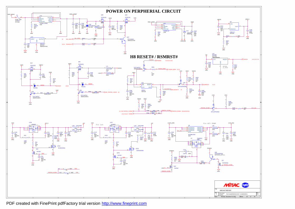
5
5
4
4
3
3
2
2
1
1
D D
C C
B B
A A
For Lan For ATI VRAM
POWER ON PERPHERIAL CIRCUIT
809S2.93V
H8 RESET# / RSMRST#
PCB 316680900001/ASSY 411680900011 R01
8050 MOTHER B/D
C
25 34Monday, December 29, 2003
Title
Size DocumentNumber
Rev
Date: Sheet of
PWRON_SUSB# VCC_ON
VCC_ON
OD3
OD5
PWRON_SUSB#
ADEN#
PWRON_SUSB#PWRON_SUSB#
OD3
PWRON_SUSB#
SW_VDD3
OD5
PWROK
THERM_ERR#
ADEN#
H8_RESET#
ADEN# 22,32
PWROK 4,12,13,17,31
KBC_PWRON_VDD3S 22
SUSB#13,17,22,23
H8_PWRON_SUSB#22 PWRON_SUSB# 26,28,29,30,31
PCIRST#013,15
SW_VDD322
THERM_ERR# 14,22
RSMRST# 13,22
H8_RESET# 22
PWROK 4,12,13,17,31
VDD1.5
VDD5
GND
GND
GND
VDD5S
GND
+5VS+3VS
GND
GND
+3VSVDD3
GND GND
+3VS+5VS +2.5VS_DDR
GND
GND
GND
GND
+3V
GND
+5V
GND GND
+2.5V_M10
GND
GND
GND
+3VS
GND
+3V
GND GND
GND GND
VDD3_AVREF
GND GND
VDD5
GNDGND
PWR_VDDIN
VDD3S
VDD3
GND
+3VS
GND GND
PWR_VDDIN
+3VS
VDD3S
GND
GND
VDD3
GNDGNDGND
+3VS VDD3
VDD3
DVMAIN
DVMAIN
GND
GND
GND
VDD3S
VDD3S
GND
GND
VDD5
+5V_H
GNDGND
C3291U0402
10V+80-20%
12
F3
FUSE_1206
1A-12063216FF-1
1 2
C284
10U6.3V080510%
12
D SG
Q48
SI2301DS
G
D S
R4564.7K/NA04025%
12
R548 0/NA 04025%
1 2
DS
Q19
2N7002G
DS
C48610U/NA
6.3V0805
10%
12
C7101U0402
10V+80-20%
12
R17 0 04025%
1 2
R551 0/NA 5%0402G_DFS1 2
DS
Q701
2N7002
G
DS
R37410K/NA04025%
12
R12480/NA0805
12
L707 120Z/100M
20121 2
C160.1U0402
50V+80-20%
12
DSG
Q722
SI2301DS/NAG
DS
L703 120Z/100M
20121 2
C5082.2U0603+/-10%
12
U10MAX809SOT23N286300690001
23
1
RESET#VCC
GN
D
R12490/NA0805
12
R5230
04025%
1 2
C7172.2U0603+/-10%
12
R1
Q44
DTC144TKA288202240001
2
13
R1Q50
DTC144TKA288202240001
2
13
C130.1U0402
50V+80-20%
12
R251220K04025%
12
R25 0/NA 5%0402G_DFS1 2
DS
Q17
2N7002/NA
G
DS
GDS
U707
AO4403SO8 8
76
4
51
32
C35510U
10V1206
12
C5174.7U0805+80-20%
12
R18 0 04025%
1 2
R53110K04025%
12
R250 1M0402 5%
1 2
R211K04025%
12
DSG
Q43
SI2301DS
G
DS
R5220/NA
04025%
1 2
C2832.2U0603+/-10%
12
C7061U0402
10V+80-20%
12
R2591K
04021%
1 2
R501
004025%
1 2
R561100K04025%
12
C7120.1U0402
50V+80-20%
12
U11
LP2951-02SO8
8273
6154
INSENSEF/BSHUTDN
5VTAPOUT
ERR-GND
R508100K04025%
12
U8
SI4788CY/NASO8
1234 5
76
8VINSOURCE1SOURCE2SOURCE3 DRAIN3
DRAIN2DRAIN1
GND
GD S
U7 SI4800DYSO8
876
4
523
1
R15
100K04025%
1 2
L71
120Z/100M2012
1 2
C2952.2U0603+/-10%
12
Q18DTA144WK/NASOT23AN_SC70_1
1
2
3
U14
LP2951-3.3/NASO8
8273
6154
INSENSEF/BSHUTDN
5VTAPOUT
ERR-GND
DS
Q10
2N7002
G
DS
C7080.1U0402
50V+80-20%
12
C38310U
6.3V0805
10%
12
R28100K04025%
12
C34210U
6.3V0805
10%
12
GDS
U704
AO4403SO8 8
76
4
51
32
R1
Q34
DTC144TKA/NA
2
1 3
U13
AMS3107SOT223286303107001
1
2
3INPUT
GN
D
OUTPUT
L704 120Z/100M
20121 2
U21
IMP811SOT143
1
2
4
3
GND
RESET
VCC
MN
C3810.1U0402
50V+80-20%
12
R705
100K04025%
1 2
DSG
Q51
SI2301DS
G
DS
C715
10U6.3V080510%
12
R480 0/NA 5%0402G_DFS1 2
U6
AME1117SOT223
1
2
3
GND/ADJ
VOUT
VIN
R3550/NA
04025%
1 2
C313
0.047U 0603
1 2
C242.2U0603+/-10%
12
D26UDZS3.6B/NASOD323
AK
R32110K04025%
12
C70510U
10V0805C
12
R1Q12
DTC144TKA288202240001
2
13
R3584.7K04025%
12
C3260.1U0402
10V10%
12
L46
120Z/100M2012
1 2
DSG
Q721
SI2301DS/NAG
DS
L72
120Z/100M/NA2012
1 2
R37510K04025%
12
C7072.2U0603+/-10%
12
R525100K04025%
12
R474294K/NA04021%
12
R36810K/NA04025%
12
R36210K04025%
12
D25RLZ3.6B/NAMLL34B
AK
D7
BAS32L
A K
C3100.1U0402
10V10%
12
R36610K/NA04025%
12
R26022K/NA
0402 1%1 2
L47
120Z/100M2012
1 2
R7071K04025%
12
R312100K04025%
12
C5060.01U0402
50V+80-20%
12
Q47
DTC144WK288202237002
1
2
3
R25320004021%
12
DSG
Q13
SI2301DS
G
DS
D13
UDZ5.6BSOD323
AK
L706 120Z/100M
20121 2
D24
BAS32L
A K
R1
Q25
DTC144TKA/NA
2
1 3
PDF created with FinePrint pdfFactory trial version http://www.fineprint.com
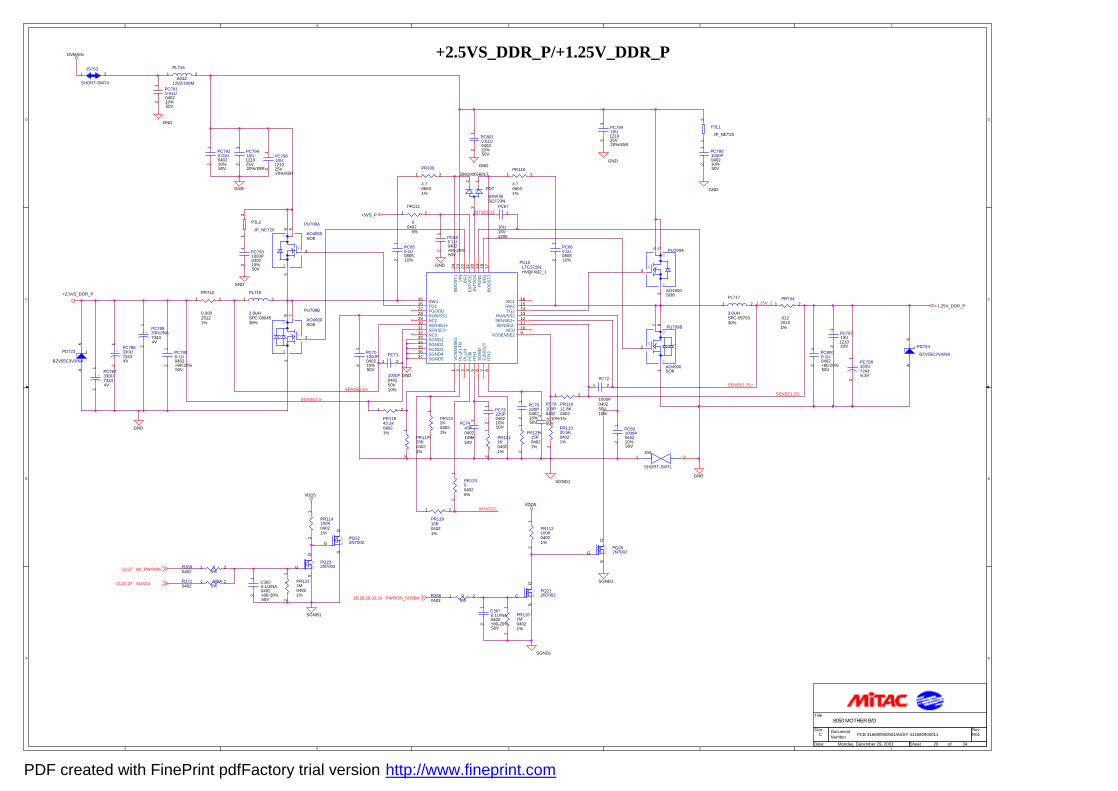
5
5
4
4
3
3
2
2
1
1
D D
C C
B B
A A
+2.5VS_DDR_P/+1.25V_DDR_P
PCB 316680900001/ASSY 411680900011 R01
8050 MOTHER B/D
C
26 34Monday, December 29, 2003
Title
Size DocumentNumber
Rev
Date: Sheet of
INTVCC1
SENSE2.5-SENSE1.25-
INTVCC1
SENSE2.5+SENSE1.25+
1.25V_2
H8_PWRON22,27
SUSC#13,22,27
PWRON_SUSB#25,28,29,30,31
+1.25V_DDR_P
SGND1
GND
GND
GND
VDD5
GND
GND
GND
GND
SGND1
DVMAIN
GND
GND
GND
+2.5VS_DDR_P
VDD5
SGND1
SGND1
+5VS_P
PR112100K04021%
12
PD723
BZV55C3V3/NA
AK
PR1211K04021%
12
DS
PQ212N7002G
DS
PR12215K04021%
12
PR1242K04021%
12
G
D
S
PU708B
AO4900SO8
2
8 71
PR110
4.706031%
1 2
C3670.1U/NA0402
50V+80-20%
12
PR1231M04021%
12
PR1151M04021%
12
PC79710U
10V1210
12
PC7920.01U0402
50V10%
12
PC680.1U0402
50V+80-20%
12
R371 0/NA0402 5%
1 2
PR111
00402
5%
1 2
PC79610U
25V1210
20%/X5R
12
PC691000P0402
50V10%
12
JS6
SHORT-SMT1
1 2
PC72
1000P040250V10%
1 2
PR11843.2K04021%
1 2
PU15LTC3728LHVQFN32_1
1 2 3 4 5 6 7 8
910111213141516
1718
3231302928272625
24 23 22 21 20 19
3334353637 V
OS
EN
SE
1P
LLFL
TRP
LLIN
FCB
ITH
1S
GN
D3.
3VO
UT
ITH
2
VOSENSE2NC0
SENSE2-SENSE2+RUN/SS2
TG2SW2NC1
BO
OS
T2B
G2
NC3SENSE1-SENSE1+NC2RUN/SS1PGOODTG1SW1
BO
OS
T1 VIN
BG
1E
XTV
CC
INTV
CC
PG
ND
SGND1SGND2SGND3SGND4SGND5
+ PC788330U73434V
12
PR744
.01220101%
1 2
PC8010.01U0402
50V10%
12
PR114100K04021%
12
PC7900.1U0402
50V+80-20%
12
PC650.1U080510%
12
PR11720K04021%
12
PC79910U
25V1210
20%/X5R
12
PC660.1U080510%
12
+ PC798150U72436.3V
12
PR109
4.706031%
1 2
PD724
BZV55C2V4/NA
AK
PL716
120Z/100M2012
1 2
PC7447P0402
50V10%
12
JS703
SHORT-SMT4
1 2
DS
PQ232N7002G
DS
D
G
S
PU709A
AO4900SO8
4
5 63
R356 00402 5%
1 2
PR120004025%
12
PR11611.8K04021%
1 2
PR11320.5K04021%
12
DS
PQ222N7002G
DS
+ PC789330U/NA73434V
12
PJL2
JP_NET20
12
PC67
10U16V1206
12
PJL1
JP_NET20
12
PC8000.1U0402
50V+80-20%
12
R369 00402 5%
1 2
G
D
S
PU709B
AO4900SO8
2
871
PC7910.01U0402
50V10%
12
PL715
3.9UHSPC-0804530%
1 2
PC71
1000P040250V10%
1 2
PR11910K04021%
1 2
PC76100P0402
50V+/-10%1
2
D
G
S
PU708A
AO4900SO8
4
563
PC7951000P0402
50V10%
12
PD7
BAW56SOT23N
288100056017
2 13
PR742
0.00825121%
1 2
PC75220P0402
50V10%
12
PC7931000P0402
50V10%
12
PC79410U
25V1210
20%/X5R
12
DS
PQ202N7002G
DS
PL717
3.0UHSPC-0570330%
1 2
C3820.1U/NA0402
50V+80-20%
12
+ PC787330U73434V
12
PC73220P0402
50V10%
12
PC701000P0402
50V10%
12
PDF created with FinePrint pdfFactory trial version http://www.fineprint.com
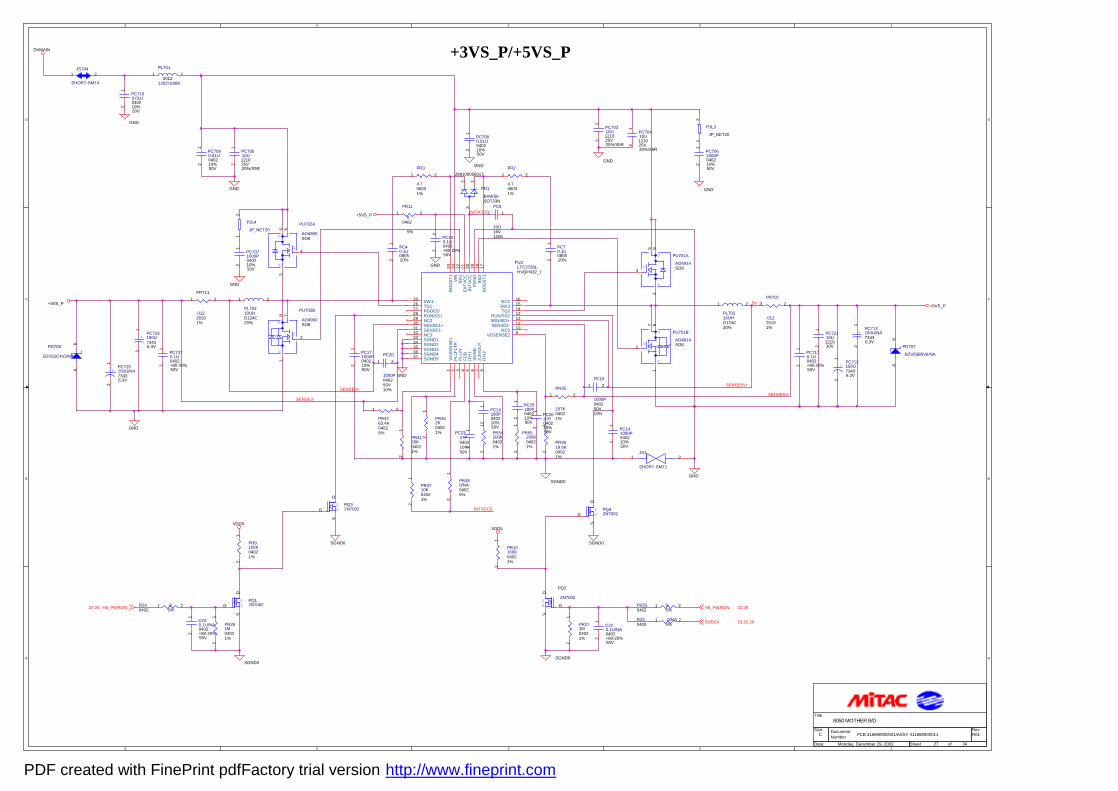
5
5
4
4
3
3
2
2
1
1
D D
C C
B B
A A
+3VS_P/+5VS_P
PCB 316680900001/ASSY 411680900011 R01
8050 MOTHER B/D
C
27 34Monday, December 29, 2003
Title
Size DocumentNumber
Rev
Date: Sheet of
5V_2
SENSE3-
SENSE3+
INTVCC0
SENSE5V-
SENSE5V+
INTVCC0
H8_PWRON22,26 H8_PWRON 22,26
SUSC# 13,22,26
VDD5
GND
+5VS_P
DVMAIN
GND
GND
GND
GND
+3VS_P
GND
GND
GND
SGND0
GND
GND
SGND0
SGND0
SGND0
+5VS_P
SGND0
VDD5
PR4710K04021%
12
PR707
.01220101%
1 2
PL701
120Z/100M2012
1 2
PC24180P0402
50V10%
12
PR9100K04021%
12
JS1
SHORT-SMT1
1 2
PR261M04021%
12
PR3
4.706031%
1 2
PR35
107K04021%
1 2
R23 0/NA0402 5%
1 2C230.1U/NA0402
50V+80-20%
12
PC19
1000P040250V10%
1 2
PR4120K04021%
12
G
D
S
PU702B
AO4900SO8
2
8 71
PJL4
JP_NET20
12
PJL3
JP_NET20
12
PR55200K04021%
12
PC20
1000P040250V10%
1 2
PD708
BZV55C4V3/NA
AK
PC40.1U080510%
12
D
G
S
PU701A
AO4914SO84
5 63PR711
.01220101%
1 2
+ PC719150U73436.3V
12
PD1
BAW56SOT23N
288100056017
2 13
PU2LTC3728LHVQFN32_1
1 2 3 4 5 6 7 8
910111213141516
1718
3231302928272625
24 23 22 21 20 19
3334353637 V
OS
EN
SE
1P
LLFL
TRP
LLIN
FCB
ITH
1S
GN
D3.
3VO
UT
ITH
2
VOSENSE2NC0
SENSE2-SENSE2+RUN/SS2
TG2SW2NC1
BO
OS
T2B
G2
NC3SENSE1-SENSE1+NC2RUN/SS1PGOODTG1SW1
BO
OS
T1 VIN
BG
1E
XTV
CC
INTV
CC
PG
ND
SGND1SGND2SGND3SGND4SGND5
DS
PQ32N7002G
DS
PR54200K04021%
12
PC70510U
25V1210
20%/X5R
12
PR11
00402
5%
1 2
PC7090.01U0402
50V10%
12
DS
PQ12N7002G
DS
+ PC713150U/NA73436.3V
12
PR462K04021%
12
PC7071000P0402
50V10%
12
+ PC712150U73436.3V
12
+ PC725150U/NA73436.3V
12
PC100.1U0402
50V+80-20%
12
PC8
10U16V1206
12
G
D
S
PU701B
AO4914SO82
871
PC70410U
25V1210
20%/X5R
12
PR10100K04021%
12
PC7080.01U0402
50V10%
12
PR2
4.706031%
1 2
PR25 00402 5%
1 2
PC7170.1U0402
50V+80-20%
12
PC70.1U080510%
12
PC70310U
25V1210
20%/X5R
12
PC7100.01U0402
50V10%
12
PR3619.6K04021%
12
JS704
SHORT-SMT4
1 2
PC7370.1U0402
50V+80-20%
12
PC2647P0402
50V10%
12
PL70210UHD124C20%
1 2
DS
PQ2
2N7002
G
DS
PR271M04021%
12
PC7061000P0402
50V10%
12
PR480/NA04025%
12
PC141000P0402
50V10%
12
D
G
S
PU702A
AO4900SO8
4
563
PC72110U
10V1210
12
R24 00402 5%
1 2
C220.1U/NA0402
50V+80-20%
12
PC171000P0402
50V10%
12
PL70310UHD124C20%
1 2
PC25180P0402
50V10%
12PR42
63.4K04025%
1 2
DS
PQ42N7002G
DS
PD707
BZV55B5V6/NA
AK
PC2347P0402
50V10%
12
PDF created with FinePrint pdfFactory trial version http://www.fineprint.com
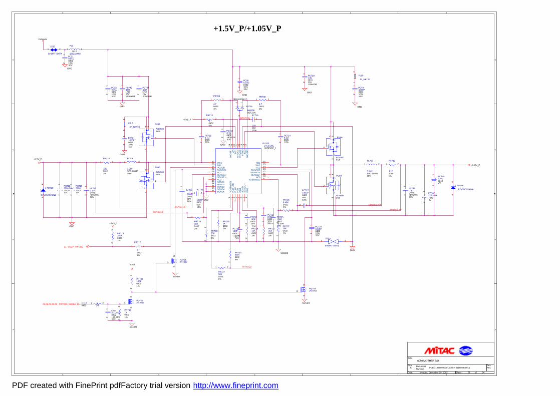
5
5
4
4
3
3
2
2
1
1
D D
C C
B B
A A
+1.5V_P/+1.05V_P
PCB 316680900001/ASSY 411680900011 R01
8050 MOTHER B/D
C
28 34Monday, December 29, 2003
Title
Size DocumentNumber
Rev
Date: Sheet of
SENSE1.5+SENSE1.05-
INTVCC3
SENSE1.05+
INTVCC3
SENSE1.5-
VCCP_PWRGD31
PWRON_SUSB#25,26,29,30,31
GND
+1.5V_P
GND
GND
SGND3
SGND3
GND
DVMAIN
SGND3
GND
VDD5
SGND3
GND
GND
GND
+1.05V_P
GND
+3VS_P
GND
+5VS_P
PL706
3.9UHSPC-0804530%
1 2
PC738180P0402
25V10%
12
PR7301M04021%
12
PC7180.1U0402
50V+80-20%
12
G
D
S
PU4B
AO4900SO8
2
8 71
PC7271000P040250V10%
12
PC736100P0402
50V+/-10%
12
PR7252K04021%
12
PJL5
JP_NET20
12
R714 00402 5%
1 2
PC310.01U0402
50V10%
12
DS
PQ7032N7002G
DS
PR719
.01220101%
1 2
PR72410K04021%
1 2
PR71818K04021%
1 2
PR733100K04021%
12
PR72220K04021%
12
PD705
BAW56SOT23N
288100056017
2 13
PC7300.1U0402
50V+80-20%
12
+ PC728220U/NA73434V
12
PU703LTC3728LHVQFN32_1
1 2 3 4 5 6 7 8
910111213141516
1718
3231302928272625
24 23 22 21 20 19
3334353637 V
OS
EN
SE
1P
LLFL
TRP
LLIN
FCB
ITH
1S
GN
D3.
3VO
UT
ITH
2
VOSENSE2NC0
SENSE2-SENSE2+RUN/SS2
TG2SW2NC1
BO
OS
T2B
G2
NC3SENSE1-SENSE1+NC2RUN/SS1PGOODTG1SW1
BO
OS
T1 VIN
BG
1E
XTV
CC
INTV
CC
PG
ND
SGND1SGND2SGND3SGND4SGND5
PR7216.49K04021%
1 2
+ PC742220U/NA73434V
12
PC734220P0402
50V10%
12
PC401000P0402
50V10%
12
JS10
SHORT-SMT4
1 2
PR709
4.706031%
1 2
PR717
004025%
1 2
PR72715K04021%
12
PC731
1000P040250V10%
1 2
PC7241000P0402
50V10%
12
PC301000P0402
50V10%
12
PC74310U
25V1210
20%/X5R
12
PC7460.1U0402
50V+80-20%
12
PR7230/NA04025%
12
PC726
1000P040250V10%
12
PL3
120Z/100M2012
1 2
PR72815K04021%
12
+ PC749220U73434V
12 PD716
BZV55C2V4/NA
AK
PR713
004025%
1 2
PC380.01U0402
50V10%
12
PR715100K04021%
12
D
G
S
PU4A
AO4900SO8
4
563
PR72620K04021%
12
G
D
S
PU6B
AO4900SO8
2
871
PC7150.1U080510%
12
PD710
BZV55C2V4/NA
AK
PR732
.01220101%
1 2
PC73910U
25V1210
20%/X5R
12
DS
PQ7062N7002G
DS
PJL6
JP_NET201
2
PC735100P0402
50V+/-10%
12
PC716
10U16V1206
12
+ PC729220U73434V
12
JS701
SHORT-SMT1
1 2
PL707
3.9UHSPC-0804530%
1 2
PC7140.1U080510%
12
C7140.1U/NA0402
50V+80-20%
12
PR708
4.706031%
1 2
PC320.01U0402
50V10%
12
PC74410U
25V1210
20%/X5R
12
DS
PQ7052N7002G
DS
D
G
S
PU6A
AO4900SO8
4
5 63
PDF created with FinePrint pdfFactory trial version http://www.fineprint.com
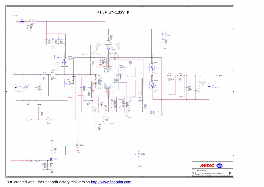
5
5
4
4
3
3
2
2
1
1
D D
C C
B B
A A
+1.8V_P/+1.35V_P
PCB 316680900001/ASSY 411680900011 R01
8050 MOTHER B/D
C
29 34Monday, December 29, 2003
Title
Size DocumentNumber
Rev
Date: Sheet of
SENSE1.2-
SENSE1.2+
INTVCC2
SENSE1.8+
1.2V_2
INTVCC2
SENSE1.8-
MCH_PG31
PWRON_SUSB#25,26,28,30,31
GND
DVMAIN
+3VS_P
GND
SGND2
SGND2
GND
VDD5
GND
GND
GND
GND
SGND2
GND
SGND2
+1.35V_P
+1.8V_P
GND
+5VS_P
PR1012K04021%
12
PR10515K04021%
12
PC7650.01U0402
50V10%
12
PC520.1U080510%
12
PR9719.6K04021%
12
PC77910U
25V1210
20%/X5R
12
PC53
10U16V1206
12
PR9919.6K04021%
12
PL714
3.0UHSPC-0670330%
1 2
PC61180P0402
50V10%
12
PR741
.01220101%
1 2
PR93100K04021%
12
PC60100P0402
50V+/-10%
12
PC7670.1U0402
50V+80-20%
12
PR10715K04021%
12
C1420.1U/NA0402
50V+80-20%
12
PR10210K04021%
1 2
PJL7
JP_NET20
12
PR103004025%
12
PL712
120Z/100M2012
1 2
PD6
BAW56SOT23N
288100056017
2 13
PC77410U
25V1210
20%/X5R
12
G
D
S
PU707B
AO4900SO8
2
871
PR9824.9K04021%
1 2
DS
PQ182N7002G
DS
D
G
S
PU705A
AO4900SO8
4
563
PR92
00402
5%
1 2
PJL8
JP_NET20
12
PC510.1U080510%
12
DS
PQ162N7002G
DS
PC7771000P0402
50V10%
12
+ PC783150U/NA73436.3V
12
PC7800.1U0402
50V+80-20%
12
R103 00402 5%
1 2
PC62100P0402
50V+/-10%
12
PR9613.7K04021%
1 2
PC7761000P0402
50V10%
12
DS
PQ172N7002G
DS
PC63180P0402
50V10%
12
G
D
S
PU705B
AO4900SO8
2
8 71
+ PC770150U73436.3V
12
PC551000P0402
50V10%
12
PD722
BZV55C2V4/NA
AK
+ PC782150U73436.3V
12
PC59
1000P040250V10%
1 2
JS706
SHORT-SMT4
1 2
PC500.01U0402
50V10%
12
PR95100K04021%
12
PL713
3.0UHSPC-0670330%
1 2
PR94
004025%
1 2
PR1061M04021%
12
JS3
SHORT-SMT1
1 2
PC57
1000P040250V10%
1 2
PC540.1U0402
50V+80-20%
12
PR91
4.706031%
1 2PR90
4.706031%
1 2
PC7660.01U0402
50V10%
12
PR739
.01220101%
1 2
PD719
BZV55C2V4/NAAK
D
G
S
PU707A
AO4900SO8
4
5 63
PU14LTC3728LHVQFN32_1
1 2 3 4 5 6 7 8
910111213141516
1718
3231302928272625
24 23 22 21 20 19
3334353637 V
OS
EN
SE
1P
LLFL
TRP
LLIN
FCB
ITH
1S
GN
D3.
3VO
UT
ITH
2
VOSENSE2NC0
SENSE2-SENSE2+RUN/SS2
TG2SW2NC1
BO
OS
T2B
G2
NC3SENSE1-SENSE1+NC2RUN/SS1PGOODTG1SW1
BO
OS
T1 VIN
BG
1E
XTV
CC
INTV
CC
PG
ND
SGND1SGND2SGND3SGND4SGND5
PC563300P0402
50V10%
12
PDF created with FinePrint pdfFactory trial version http://www.fineprint.com
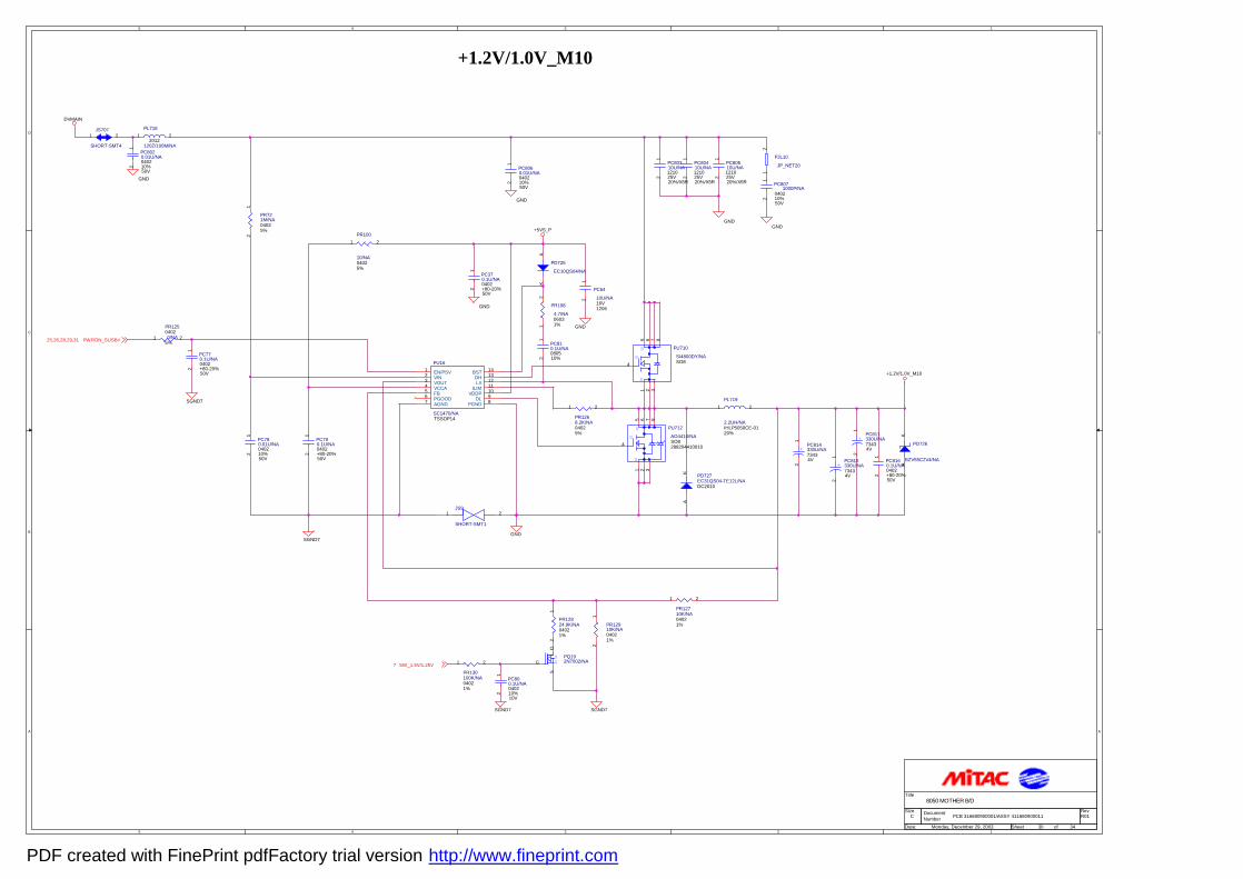
5
5
4
4
3
3
2
2
1
1
D D
C C
B B
A A
+1.2V/1.0V_M10
PCB 316680900001/ASSY 411680900011 R01
8050 MOTHER B/D
C
30 34Monday, December 29, 2003
Title
Size DocumentNumber
Rev
Date: Sheet of
SW_1.5V/1.25V7
PWRON_SUSB#25,26,28,29,31
DVMAIN
GND
SGND7GND
GND
SGND7
GND
GND
SGND7 SGND7
+5VS_P
GND
+1.2V/1.0V_M10
GND
PC780.01U/NA0402
50V10%
12
PD727EC31QS04-TE12L/NADC2010
AK
GD
S
PU712
AO4410/NASO8288204410010
876
4
52 31
PC64
10U/NA16V1206
12
JS707
SHORT-SMT4
1 2
PC8071000P/NA
0402
50V10%
12
GD
S
PU710
SI4800DY/NASO8
876
4
52 31
PR130100K/NA04021%
1 2
PC370.1U/NA0402
50V+80-20%
12
PD725
EC10QS04/NA
AK
PR100
10/NA04025%
1 2
PC8020.01U/NA0402
50V10%
12
PR721M/NA04025%
12
PR12710K/NA04021%
1 2
PR108
4.7/NA06031%1
2
+ PC814330U/NA73434V
12
PC8160.1U/NA0402
50V+80-20%
12
PU16
SC1470/NATSSOP14
34
876
2
5
1
91011121314
VOUTVCCA
PGNDAGNDPGOOD
VIN
FB
EN/PSV
DLVDDP
ILIMLXDH
BST
PC80310U/NA
25V1210
20%/X5R
12
PC80510U/NA
25V1210
20%/X5R
12
PL718
120Z/100M/NA2012
1 2
PL719
2.2UH/NAIHLP5050CE-0120%
1 2
JS9
SHORT-SMT1
1 2
PC80410U/NA
25V1210
20%/X5R
12
PC790.1U/NA0402
50V+80-20%
12
PR125
0/NA0402
5%1 2
PC770.1U/NA0402
50V+80-20%
12
PC810.1U/NA080510%
12
DS
PQ192N7002/NAG
DS
PC8060.01U/NA0402
50V10%
12
+ PC815330U/NA73434V
12
PR12910K/NA04021%
12
PJL10
JP_NET20
12
PC800.1U/NA0402
10V10%
12
PD726
BZV55C2V4/NA
AK
PR1268.2K/NA04025%
1 2
+ PC811330U/NA73434V
12
PR12824.9K/NA04021%
12
PDF created with FinePrint pdfFactory trial version http://www.fineprint.com
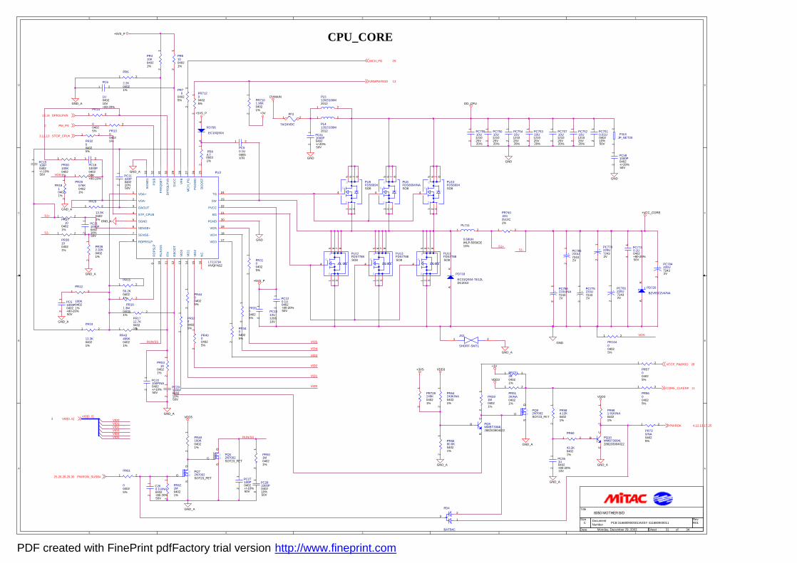
5
5
4
4
3
3
2
2
1
1
D D
C C
B B
A A
CPU_CORE
PCB 316680900001/ASSY 411680900011 R01
8050 MOTHER B/D
C
31 34Monday, December 29, 2003
Title
Size DocumentNumber
Rev
Date: Sheet of
VID[0..5]
S1+
S1-
VID5RUN/SS
VID4
VID3
VID2
VID1
VID0
S1+S1-
VOS-
VOS-
RUN/SSVID4VID5
VID0VID1VID2VID3
MCH_PG 29
VRMPWRGD 13
VCCP_PWRGD 28
PWROK 4,12,13,17,25
VID[0..5]3
PM_PS2
DPRSLPVR13,14
STOP_CPU#3,11,13
CORE_CLKEN# 11
PWRON_SUSB#25,26,28,29,30
GND_A
VDD5
GND
+3V
GND_A
GND_A
GND_A
GND
DVMAIN
GND_A
GND_A
GND_A
GND
+VCC_CORE
DD_CPU
GND
GND_A
VDD3
GND
GND_A
GND_A
GND_A
GND_A
VDD3
VDD3
+5VS_P
+5VS_P
+5VS_P
+3V+3VS
GND_A
PR44004025%
12
PR501M04021%
12
PC15100P0402
50V+/-10%
12
GD
S
PU12FDS7788SO8
876
4
52 31
+ PC778220U72432V
12PR31
004025%
12
PC6
1U040210V+80-20%
1 2
PR52004025%
12
PC75210U
25V1210
20%
12
PR40004025%
12
+ PC785220U72432V
12
PD720
BZV55C2V4/NA
AK
PR621M04021%
12
DS
PQ82N7002SOT23_FET
G
DS
PR161.3M04021%
1 2
PR381004021%
1 2
PR19
13.3K04021%
1 2
GD
S
PU13FDS7788SO8
876
4
52 31
PD718
EC31QS04-TE12LDC2010
AK
PR51004021%
12
PR56004025%
1 2
PC211000P0402
50V10%
12
PL5120Z/100M2012
1 2
PQ10MMBT3904L288203904022
B
EC
+ PC784220U72432V
12
PC7510.01U0402
50V10%
12
PC51000P0402
50V+80-20%
12
PR43499K04021%
1 2
PC7730.1U0402
50V+80-20%
12
PC75010U
25V1210
20%
12
PR392.32K04021%
12
PR681.91K/NA04021%
12
PR591M04021%
12
PC411000P0402
50V+/-20%
12
PR32004025%
1 2
GD
S
PU10FDS6694SO8
876
4
52 31
PR60
43.2K04021%
1 2
GD
S
PU8FDS6694/NASO8
876
4
52 31
PR584.12K04021%
12
PU3
LTC3734HVQFN32
1
2
3
5
6
7
8
4
9 10 11 12 13 14 15 16
17
18
19
20
21
22
23
24
252627282930313233
VOA+
VOA-
OAOUT
SGND
SENSE+
SENSE-
RDPRSLP
STP_CPUB
RD
PS
LP
RU
N/S
S
ITH
RB
OO
T
VID
0
VID
1
VID
2
NC
VID3
VID4
VID5
PGND
BG
PVCC
SW
TG
BO
OS
T
PG
OO
D
MC
H_P
G
VFB
SV
CC
DP
RS
LPV
R
FRE
QS
ET
PS
IB
SG
ND
1
PF2
7A/24VDC
1 2
PR13004025%
1 2
PD4
BAT54C
1
23
PR730/NA04025%
1 2
+ PC786220U/NA72432V
12
PJL9JP_NET20
12
PC181000P040250V+80-20%
1 2
PC90.1U0805X7R
1 2
PR740.0012512C1%
1 2
PC75710U
25V1210
20%
12
PC291000P0402
50V10%
12
GD
S
PU9FDS6694SO8
876
4
52 31
PR84.706031%
12
PC1310U
10V1206
12
PR6
2.2K04021%
1 2
PR64249K/NA04021%
12
PR70
04025%
12
PC75510U
25V1210
20%
12
PC75310U
25V1210
20%
12
+ PC781220U72432V
12
PR410K04021%
12
PC22100P/NA0402
50V+/-10%
12
PR14
004025%
1 2
PD706
EC10QS04
AK
PC75410U
25V1210
20%
12
PC283300P0402
50V10%
12
PL711
0.68UHIHLP-5050CE15%
1 2
PR7312K04021%
1 2
PR3710
04021%
1 2
PC11220P0402
50V10%
12
PR7101.96K04021%
12
PR49100K04021%
12
PR15
56.2K04021%
1 2PR12
100K04021%
1 2
PR712004025%
12
PR512K/NA04021%
1 2
PR1712.7K04021%
1 2
DS
PQ72N7002SOT23_FET
G
DS
+ PC775220U72432V
12
PC581000P0402
50V+/-20%
12
C260.1U/NA0402
50V+80-20%
12
PR28576K04021%
1 2
PR6680.6K04021%
12
PC120.1U0402
50V+80-20%
12PR33
004025%
12
DS
PQ52N7002SOT23_FET
G
DS
PR29
13.3K04021%
1 2
PC27100P0402
50V+/-10%
12
PR729249K04021%
12
PR18104021%
12
PR61
004025%
1 2
PC351U0402
10V+80-20%
12
PR104004025%
1 2
PR30100K04021%
1 2
GD
S
PU11FDS7788SO8
876
4
52 31
PR34004025%
12
PL4120Z/100M2012
1 2
JS2
SHORT-SMT1
1 2
PR57004025%
1 2
PQ9MMBT3904L288203904022
B
EC
PR531K
04021%
12
PDF created with FinePrint pdfFactory trial version http://www.fineprint.com
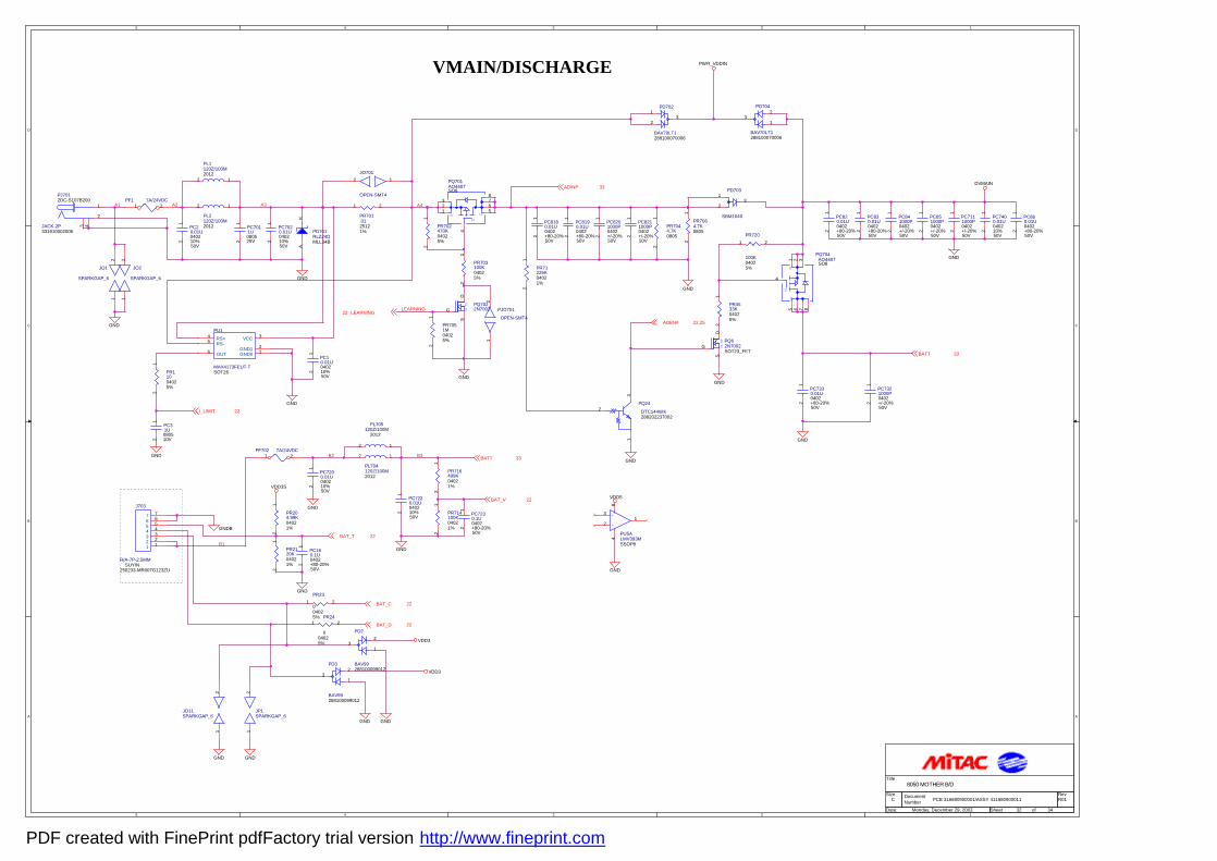
5
5
4
4
3
3
2
2
1
1
D D
C C
B B
A A
VMAIN/DISCHARGE
PCB 316680900001/ASSY 411680900011 R01
8050 MOTHER B/D
C
32 34Monday, December 29, 2003
Title
Size DocumentNumber
Rev
Date: Sheet of
B1
A1
LEARNING
A2 A4
B2 B3
A3
I_LIMIT 22
LEARNING22
BATT 33
BAT_V 22
BAT_T 22
BAT_C 22
BAT_D 22
ADEN# 22,25
BATT 33
ADINP 33
VDD3
VDD3
GND
GND
GND
GNDB
PWR_VDDIN
GND
GND
GND
GND
GND
GND
GND
GND
GND
GND
VDD3S
DVMAIN
GND
GND
GND
GND
VDD5
GND
PR703100K04025%
12
PC10.01U0402
50V10%
12PR1
1004025%
12
PR716499K04021%
12
PD702
BAV70LT1288100070006
1
23
PR720
100K04025%
1 2
PD701RLZ24DMLL34B
AK
PD3
BAV99288100099012
1
23
PQ24
DTC144WK288202237002
1
2
3
PR24
004025%
1 2
PC8190.01U0402
50V+80-20%
12
PC860.01U0402
50V+80-20%
12
PL1120Z/100M2012
12
PC31U
10V0805
12
+
-PU5ALMV393MSSOP8
3
21
84
JP1SPARKGAP_6
12
JO11SPARKGAP_6
12
PC7011U
25V0805
12
PJ701
JACK-2P
2DC-S107B200
331910002006
2
1
3 4
PC7400.01U0402
50V10%
12
PC851000P0402
50V+/-20%
12
PC8201000P0402
50V+/-20%
12
PR701.0125121%
1 2
PJO701
OPEN-SMT4
12
PC7200.01U0402
50V10%
12
DS
PQ62N7002SOT23_FET
G
DS
PR71226K04021%
12
JO701
OPEN-SMT4
12
GDS
PQ701AO4407SO8
876
4
51
32
J703
R/A-7P-2.5MMSUYIN
250233-MR007G123ZU
1234567
1234567
PC820.01U0402
50V+80-20%
12
PC7330.01U0402
50V+80-20%
12
PD704
BAV70LT1288100070006
1
23
JO1
SPARKGAP_6
12
PF702 7A/24VDC1 2
PC7321000P0402
50V+/-20%
12
JO2
SPARKGAP_6
12
PD2
BAV99288100099012
1
23
DS
PQ7022N7002G
DS
PC8180.01U0402
50V+80-20%
12
PR714100K04021%
12
PC7220.01U0402
50V10%
12
PC20.01U0402
50V10%
12
PD703
SBM1040
1
23
PR2120K04021%
12
PL705120Z/100M
2012
12
PR204.99K04021%
12
PL2120Z/100M2012
12
PR23
004025%
1 2
PC7230.1U0402
50V+80-20%
12
PR7044.7K0805
12
PR7051M04025%
12
PF1 7A/24VDC1 2
PC830.01U0402
50V+80-20%
12
PR4533K04025%
12
PC160.1U0402
50V+80-20%
12
PC8211000P0402
50V+/-20%
12
PC7020.01U0402
50V10%
12
PC841000P0402
50V+/-20%
12
PL704120Z/100M2012
12
PR7064.7K0805
12
PR702470K04025%
12
PU1
MAX4173FEUT-TSOT26
162
354
GND0OUTGND1
VCCRS-RS+
GD
S
PQ704AO4407SO8
876
4
51 32
PC7111000P0402
50V+/-20%
12
PDF created with FinePrint pdfFactory trial version http://www.fineprint.com
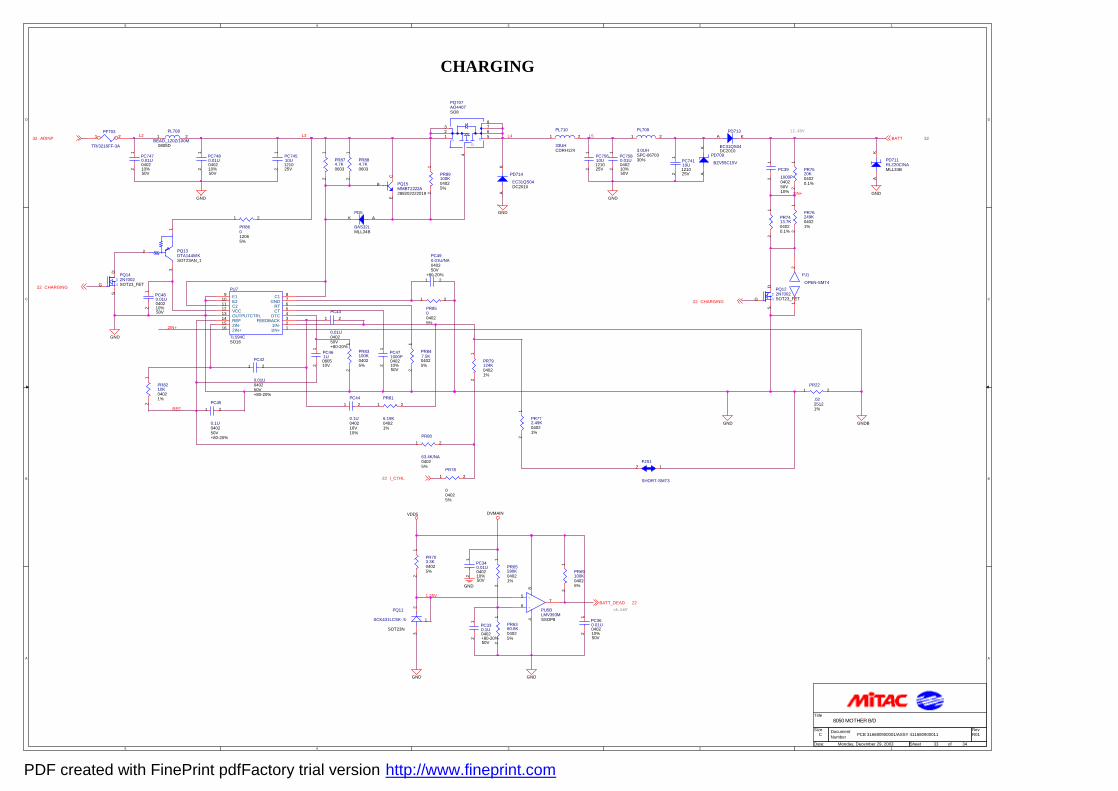
5
5
4
4
3
3
2
2
1
1
D D
C C
B B
A A
CHARGING
=8.56V
12.65V
PCB 316680900001/ASSY 411680900011 R01
8050 MOTHER B/D
C
33 34Monday, December 29, 2003
Title
Size DocumentNumber
Rev
Date: Sheet of
1.25V
L2
REF
2IN+
L4L3 L5
2IN+
ADINP32 BATT 32
BATT_DEAD 22
I_CTRL22
CHARGING22
CHARGING22
VDD5
GND
GND GNDB
GND
GND
GND
GND
GND
GND
DVMAIN
GND
DS
PQ142N7002SOT23_FETG
DS
+
-PU5BLMV393MSSOP8
5
67
84
PC42
0.01U040250V+80-20%
1 2
PC39
1000P040250V10%
12
PC480.01U0402
50V10%
12
PC340.01U0402
50V10%
12
PR65590K04021%
12
PC490.01U/NA040250V
+80-20%1 2
PD713
EC31QS04DC2010
A K
PR69100K04025%
12
PR76249K04021%
12
PR6380.6K04025%
12
PC43
0.01U040250V+80-20%
1 2
PD5
BAS32LMLL34B
AK
PR847.5K04025%
12
PR85004025%
1 2
PR79124K04021%
12
PL708
BEAD_120Z/100M0805D
1 2
DS
PQ122N7002SOT23_FETG
DS
PR8210K04021%
12
PC74110U
25V1210
12
PC45
0.1U040250V+80-20%
1 2
PJ1
OPEN-SMT4
12
PR703.3K04025%
12
PC74510U
25V1210
12
PL709
3.0UHSPC-0670330%
1 2
PD714
EC31QS04DC2010
AK
PR80
63.4K/NA04025%
1 2
PC7480.01U0402
50V10%
12
PR81
6.19K04021%
1 2
PR86012065%
1 2
PC461U
10V0805
12
PC75610U
25V1210
12
PR772.49K04021%
12
PC330.1U0402
50V+80-20%
12
PR7413.7K04020.1%
12
PR22
.0225121%
1 2
PC471000P0402
50V10%
12
PU7
TL594CSO16
123456789
10111213141516 1IN+
1IN-FEEDBACK
DTCCTRT
GNDC1E1
E2C2VCCOUTPUTCTRLREF2IN-2IN+
PC44
0.1U040216V10%
1 2
GDS
PQ707AO4407SO8
876
4
51
32
PR89100K04025%
12
PJS1
SHORT-SMT3
12
PC360.01U0402
50V10%
12
PF703
TR/3216FF-3A
1 2
PR874.7K0603
12
PQ15MMBT2222A288202222019
B
EC
PR83100K04025%
12
PD711RLZ20C/NAMLL34B
AK
PQ11
SCK431LCSK-.5
SOT23N
32
1
PC7470.01U0402
50V10%
12
PC7580.01U0402
50V10%
12 PR75
20K04020.1%
12
PQ13DTA144WKSOT23AN_1
1
2
3
PR78
004025%
1 2
PD709
BZV55C15V
AK
PL710
33UHCDRH124
1 2
PR884.7K0603
12
PDF created with FinePrint pdfFactory trial version http://www.fineprint.com

5
5
4
4
3
3
2
2
1
1
D D
C C
B B
A A
855GME
MINIPCI
33MH
Z
CLOCK GENERATOR
Keyboard BIOS
SMBU
S
IEEE1394
ICS950810
CPU_THRMDA/CPU_THRMDC
HDD
North Bridge
W83L950D
HP JACK
25MHZ
BATT-Adapter
VIAVT6307L
D/D PowerLTC3728L
DDR 266
WINBOND
I-LIMIT OP
D/D PowerLTC3728L
USBCLK_ICH
HCLK_NB+/- 100MHZ
PRIMARY IDE
EXTMIC.
Sourth Bridge
D/D ChargerTL-594C
PCIC
LK_M
INIP
CI
RGB
24.576MHZ
32.768KHZ
+3V/+5V
SECONDARY IDE
PCMCIA
D/D
SYSTEM
MAX4173F
AUDIO
48MHZ
ALC655
66M_MCH
33MH
Z
512K
LVDS
MODULE
ICH4-M
InternalKeyboard
AC-AdapterPCICLK_ICH 33MHZ
PCIPCI_
1394
_CLK
I -LIMIT
BIOS
Fan
INT MIC
MDC
LPC BUS
CPU INTELBANIAS/DOTHAN
24.576MHZ / NA
PS/2
(XGA)
CODEC
I -LIMIT
8MHZ
PCI_
CRAD
_CLK
66M_ICH
DREFCLK_48MHZ
AMPLIFIER
AC97
33MH
Z
PCMCIA/CARDBUSSLOT
D/D CPU CoreLTC3734
KEY
MA
TRIX
TPA0212
SPEAKER
TOUCH
LCD PANEL
CDROM
ADT7460
66MHZ
PAD
+2.5V/+1.25V
VGA_M10AGP
27MHZ
LVDS/NARGB/NA
CRT
TVCH7011
HCLK_CPU+/- 100MHZCLK_ITP_CPU+/- 100MHZ
66M_AGP
14M_CODEC
14M_CODEC (CLK GEN)
14.318MHZ
PCIC
LK_F
WH
USB 0~2x3
14M_ICH
CARD READER
NA
RTL8100CLPCICLK_LAN
RJ45/ RJ11
PH163112
SIO_48M(DEBUG CARD ONLY)
DIMM0
CLK_DDR4+/-CLK_DDR5+/-
CLK_DDR3+/-CLK_DDR0+/-
DIMM1CLK_DDR1+/-CLK_DDR2+/-
VGA_THRMDA/VGA_THRMDC
VRAM16MBx4
SPEAKERLM4871
SUB WOOFER
LINEIN
HOST 400MHZ
66MHZ
D/D PowerLTC3728L+1.5V/+1.05V
D/D PowerLTC3728L
8050 BLOCK DIAGRAM
CARD REARDERSOCKET
CardReaderTransition Board
CABLE
CB710
CP2211
D/D PowerSC1470+1.2V/1.0V +1.8V /+1.35V
PCB 316680900001/ASSY 411680900011 R01
8050 MOTHER B/D
C
34 34Monday, December 29, 2003
Title
Size DocumentNumber
Rev
Date: Sheet of
PDF created with FinePrint pdfFactory trial version http://www.fineprint.com
REFERENCE MATERIAL
System Explode View
Intel Mobile Pentium-M Processor/BANIAS Processor Intel, INC.
…Intel 855GME North Bridge’ Intel, INC.
…Intel ICH-4 South Bridge’
8050 Hardware Specification
WINBOND, LTD.
Intel, INC.
Technology Corp / MiTAC
WINBOND KBC
Technology Corp / MiTAC
VT6307L IEEE1394 Host Controller AMPRO Computers, INC
Clock Syntherizer ICS,INC
SERVICE MANUAL FOR 8050SERVICE MANUAL FOR SERVICE MANUAL FOR 8050
Sponsoring Editor : Jesse Jan
Author : Grass Ren
Assistant Editor : Ping.Xie
Publisher : MiTAC International Corp.
Address : 1, R&D Road 2, Hsinchu Science-Based Industrial, Hsinchu, Taiwan, R.O.C.
Tel : 886-3-5779250 Fax : 886-3-5781245
First Edition : Feb.2004
E-mail : Willy .Chen @ mic.com.tw
Web : http: //www.mitac.com http: //www.mitacservice.com