S-19110AxxA to S-19110HxxA Series VOLTAGE DETECTOR · · 2017-12-22product, so the output is ......
49
S-19110AxxA to S-19110HxxA Series www.ablicinc.com FOR AUTOMOTIVE 125°C OPERATION HIGH-WITHSTAND VOLTAGE BUILT-IN DELAY CIRCUIT (EXTERNAL DELAY TIME SETTING) VOLTAGE DETECTOR © ABLIC Inc., 2014-2016 Rev.1.3_01 1 The S-19110 Series is a high-accuracy voltage detector developed using CMOS technology. The detection voltage and release voltage are fixed internally with an accuracy of 2.0%. It operates with current consumption of 600 nA typ. Apart from the power supply pin, the detection voltage input pin (SENSE pin) is also prepared in the SENSE detection product, so the output is stable even if the SENSE pin falls to 0 V. The detection signal and release signal can be delayed by setting a capacitor externally, and the detection delay time accuracy is 20% (C N = 3.3 nF, Ta = 40°C to 125°C), the release delay time accuracy is 20% (C P = 3.3 nF, Ta = 40°C to 125°C). The output form is Nch open-drain output. Caution This product can be used in vehicle equipment and in-vehicle equipment. Before using the product in the purpose, contact to ABLIC Inc. is indispensable. Features Detection voltage: 5.0 V to 10.0 V (0.05 V step) Detection voltage accuracy: 2.0% (Ta = 40°C to 125°C) Detection delay time accuracy: 20% (C N = 3.3 nF, Ta = 40°C to 125°C) Release voltage: 5.25 V to 13.0 V (0.05 V step) Release voltage accuracy: 2.0% (Ta = 40°C to 125°C, 5.0% V HYS 20.0%) 2.5% (Ta = 40°C to 125°C, 20.0% V HYS 30.0%) Release delay time accuracy: 20% (C P = 3.3 nF, Ta = 40°C to 125°C) Current consumption: 600 nA typ. Operation voltage range: 1.8 V to 36.0 V Hysteresis width *1 : "Available" / "unavailable" is selectable. 5.0% to 30.0% (Ta = 40°C to 125°C) Output form: Nch open-drain output Operation temperature range: Ta = 40°C to 125°C Lead-free (Sn 100%), halogen-free AEC-Q100 qualified *2 *1. When "available" is selected, the hysteresis width can be set in the range of 5.0% to 30.0%. *2. Contact our sales office for details. Applications Power supply monitor for microcomputer and reset for CPU Automotive battery voltage detection For automotive use (engine, transmission, suspension, ABS, related-devices for EV / HEV / PHEV, etc.) Package SOT-23-6
Transcript of S-19110AxxA to S-19110HxxA Series VOLTAGE DETECTOR · · 2017-12-22product, so the output is ......

S-19110AxxA to S-19110HxxA Series
www.ablicinc.com
FOR AUTOMOTIVE 125°C OPERATION HIGH-WITHSTAND VOLTAGE BUILT-IN DELAY CIRCUIT (EXTERNAL DELAY TIME SETTING) VOLTAGE DETECTOR
© ABLIC Inc., 2014-2016 Rev.1.3_01
1
The S-19110 Series is a high-accuracy voltage detector developed using CMOS technology. The detection voltage and release voltage are fixed internally with an accuracy of 2.0%. It operates with current consumption of 600 nA typ. Apart from the power supply pin, the detection voltage input pin (SENSE pin) is also prepared in the SENSE detection product, so the output is stable even if the SENSE pin falls to 0 V. The detection signal and release signal can be delayed by setting a capacitor externally, and the detection delay time accuracy is 20% (CN = 3.3 nF, Ta = 40°C to 125°C), the release delay time accuracy is 20% (CP = 3.3 nF, Ta = 40°C to 125°C). The output form is Nch open-drain output. Caution This product can be used in vehicle equipment and in-vehicle equipment. Before using the product in
the purpose, contact to ABLIC Inc. is indispensable.
Features
Detection voltage: 5.0 V to 10.0 V (0.05 V step) Detection voltage accuracy: 2.0% (Ta = 40°C to 125°C) Detection delay time accuracy: 20% (CN = 3.3 nF, Ta = 40°C to 125°C) Release voltage: 5.25 V to 13.0 V (0.05 V step) Release voltage accuracy: 2.0% (Ta = 40°C to 125°C, 5.0% VHYS 20.0%) 2.5% (Ta = 40°C to 125°C, 20.0% VHYS 30.0%) Release delay time accuracy: 20% (CP = 3.3 nF, Ta = 40°C to 125°C) Current consumption: 600 nA typ. Operation voltage range: 1.8 V to 36.0 V Hysteresis width*1: "Available" / "unavailable" is selectable. 5.0% to 30.0% (Ta = 40°C to 125°C) Output form: Nch open-drain output Operation temperature range: Ta = 40°C to 125°C Lead-free (Sn 100%), halogen-free AEC-Q100 qualified*2
*1. When "available" is selected, the hysteresis width can be set in the range of 5.0% to 30.0%. *2. Contact our sales office for details.
Applications
Power supply monitor for microcomputer and reset for CPU Automotive battery voltage detection For automotive use (engine, transmission, suspension, ABS, related-devices for EV / HEV / PHEV, etc.)
Package
SOT-23-6

FOR AUTOMOTIVE 125°C OPERATION HIGH-WITHSTAND VOLTAGE BUILT-IN DELAY CIRCUIT (EXTERNAL DELAY TIME SETTING) VOLTAGE DETECTOR S-19110AxxA to S-19110HxxA Series Rev.1.3_01
2
Block Diagrams
1. S-19110 Series A / B type (VDD detection product)
VSS
*1
*1
VREF
OUT
VDD
CN
Delaycircuit
*1
CP
*1
Function Status
Voltage detection VDD detection
Hysteresis width Available
*1. Parasitic diode
Figure 1
2. S-19110 Series C / D type (VDD detection product)
VSS
*1
*1
VREF
OUT
VDD
CN
Delaycircuit
*1
CP
*1
Function Status
Voltage detection VDD detection
Hysteresis width Unavailable
*1. Parasitic diode
Figure 2

FOR AUTOMOTIVE 125°C OPERATION HIGH-WITHSTAND VOLTAGE BUILT-IN DELAY CIRCUIT (EXTERNAL DELAY TIME SETTING) VOLTAGE DETECTORRev.1.3_01 S-19110AxxA to S-19110HxxA Series
3
3. S-19110 Series E / F type (SENSE detection product)
VSS
*1
*1VREF
OUT
VDD
CN
Delaycircuit
*1
*1
*1
CPSENSE
Function Status
Voltage detection SENSE detection
Hysteresis width Available
*1. Parasitic diode
Figure 3
4. S-19110 Series G / H type (SENSE detection product)
VSS
*1
*1VREF
OUT
VDD
CN
Delaycircuit
*1
*1
*1
CPSENSE
Function Status
Voltage detection SENSE detection
Hysteresis width Unavailable
*1. Parasitic diode
Figure 4

FOR AUTOMOTIVE 125°C OPERATION HIGH-WITHSTAND VOLTAGE BUILT-IN DELAY CIRCUIT (EXTERNAL DELAY TIME SETTING) VOLTAGE DETECTOR S-19110AxxA to S-19110HxxA Series Rev.1.3_01
4
AEC-Q100 Qualified This IC supports AEC-Q100 for operation temperature grade 1. Contact our sales office for details of AEC-Q100 reliability specification.
Product Name Structure
Users can select the product type, detection voltage value and release voltage value for the S-19110 Series. Refer to "1. Product name" regarding the contents of product name, "2. Function list of product types" regarding the product types and "3. Package" regarding the package drawings.
1. Product name
S-19110 x xx A - M6T1 U 4
Package abbreviation and IC packing specifications*1 M6T1 : SOT-23-6, Tape
Detection voltage value, release voltage value*2 AA to ZZ (2-digit alphabetical option code)
Environmental code U : Lead-free (Sn 100%), halogen-free
Operation temperature A : Ta = 40C to 125C
Product type*3 A to H
*1. Refer to the tape drawing. *2. Contact our sales office for details on combination of detection voltage value and release voltage value. *3. Refer to "2. Function list of product types".

FOR AUTOMOTIVE 125°C OPERATION HIGH-WITHSTAND VOLTAGE BUILT-IN DELAY CIRCUIT (EXTERNAL DELAY TIME SETTING) VOLTAGE DETECTORRev.1.3_01 S-19110AxxA to S-19110HxxA Series
5
Remark 1. The difference (hysteresis width) of detection voltage (VDET) and release voltage (VDET) can be set in the range of 5.0% to 30.0%. The detection voltage and release voltage combination can be selected from the A area shown in Figure 5.
Example: If VDET = 5.0 V, the release voltage can be set in the range of 5.25 V to 6.5 V in 50 mV
step.
13.012.011.0
5.05.0 10.0
VDET [V]9.08.07.06.0
VD
ET
[V]
10.09.08.07.06.0
A
Figure 5 Detection Voltage and Release Voltage Possible Setting Area (VDET 10.0 V) 2. The detection voltage in the S-19110 Series, which is 10.0 V max., is the release voltage in B area
shown in Figure 6 in SENSE detection product with VDET = 10.0 V. When setting the detection voltage exceeding 10.0 V with an external resistor, the difference of detection voltage and release voltage can be set in the range of 5.0% to 30.0%.
Refer to "2. SENSE pin" in " Operation" for details.
13.513.012.5
10.09.5 10.5
VDET [V]10.0
VD
ET
[V]
12.011.511.010.5
B
Figure 6 Detection Voltage and Release Voltage Possible Setting Area (VDET 10.0 V)
2. Function list of product types
Table 1
Product Type Voltage Detection Output Logic Hysteresis Width
A VDD detection Active "L" Available
B VDD detection Active "H" Available
C VDD detection Active "L" Unavailable
D VDD detection Active "H" Unavailable
E SENSE detection Active "L" Available
F SENSE detection Active "H" Available
G SENSE detection Active "L" Unavailable
H SENSE detection Active "H" Unavailable
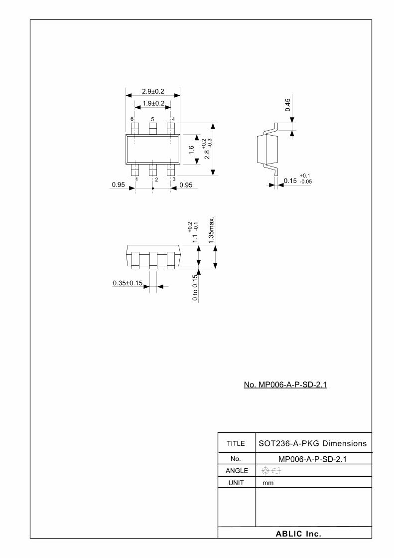
3. Package
Table 2 Package Drawing Codes
Package Name Dimension Tape Reel
SOT-23-6 MP006-A-P-SD MP006-A-C-SD MP006-A-R-SD

FOR AUTOMOTIVE 125°C OPERATION HIGH-WITHSTAND VOLTAGE BUILT-IN DELAY CIRCUIT (EXTERNAL DELAY TIME SETTING) VOLTAGE DETECTOR S-19110AxxA to S-19110HxxA Series Rev.1.3_01
6
Pin Configurations
1. S-19110 Series A / B / C / D type (VDD detection product)
1. 1 SOT-23-6
1 32
5 46
Top view
Figure 7
Table 3
Pin No. Symbol Description
1 VDD Voltage input pin
2 NC*1 No connection
3 OUT Voltage detection output pin
4 CP*2 Connection pin for release delay capacitor
5 VSS GND pin
6 CN*3 Connection pin for detection delay capacitor
*1. The NC pin is electrically open. The NC pin can be connected to the VDD pin or the VSS pin. *2. Connect a capacitor between the CP pin and the VSS pin. The release delay time can be adjusted according to the capacitance. Moreover, the CP pin is available even when it is open. *3. Connect a capacitor between the CN pin and the VSS pin.
The detection delay time can be adjusted according to the capacitance. Moreover, the CN pin is available even when it is open.
2. S-19110 Series E / F / G / H type (SENSE detection product)
2. 1 SOT-23-6
1 32
5 46
Top view
Figure 8
Table 4
Pin No. Symbol Description
1 VDD Voltage input pin
2 SENSE Detection voltage input pin
3 OUT Voltage detection output pin
4 CP*1 Connection pin for release delay capacitor
5 VSS GND pin
6 CN*2 Connection pin for detection delay capacitor
*1. Connect a capacitor between the CP pin and the VSS pin. The release delay time can be adjusted according to the capacitance. Moreover, the CP pin is available even when it is open. *2. Connect a capacitor between the CN pin and the VSS pin.
The detection delay time can be adjusted according to the capacitance.Moreover, the CN pin is available even when it is open.
FOR AUTOMOTIVE 125°C OPERATION HIGH-WITHSTAND VOLTAGE BUILT-IN DELAY CIRCUIT (EXTERNAL DELAY TIME SETTING) VOLTAGE DETECTORRev.1.3_01 S-19110AxxA to S-19110HxxA Series
7
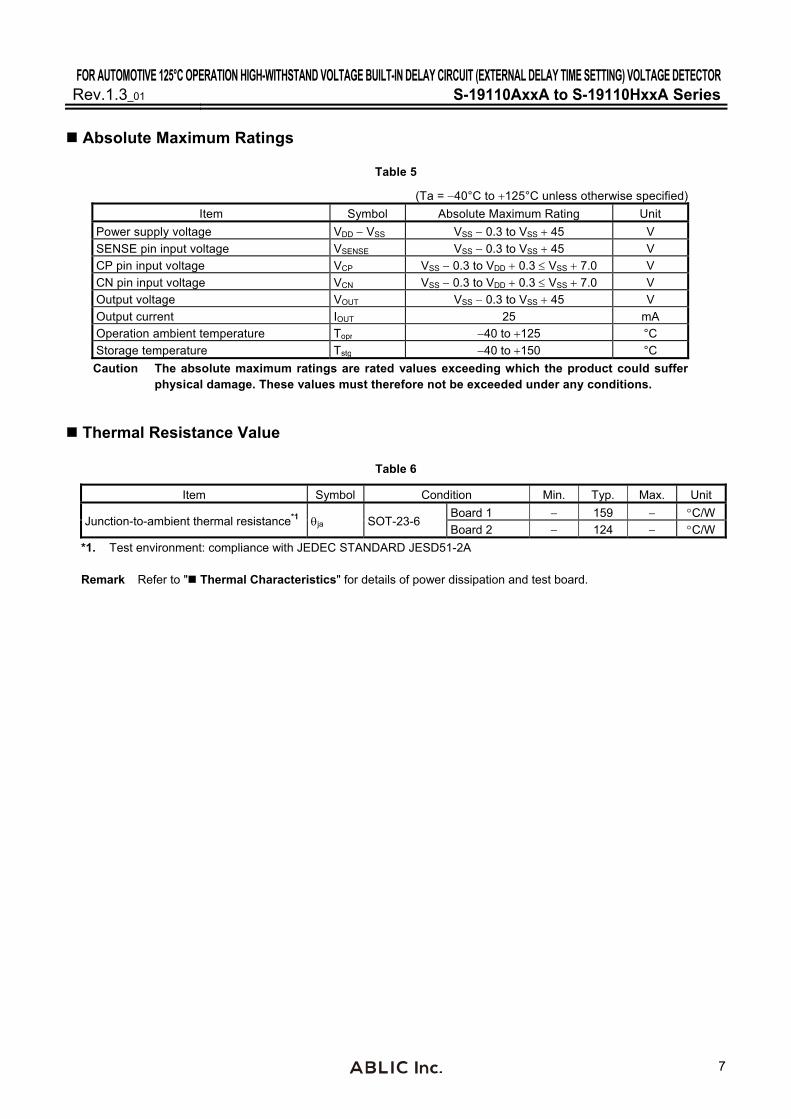
Absolute Maximum Ratings
Table 5
(Ta = 40°C to 125°C unless otherwise specified)
Item Symbol Absolute Maximum Rating Unit
Power supply voltage VDD VSS VSS 0.3 to VSS 45 V
SENSE pin input voltage VSENSE VSS 0.3 to VSS 45 V
CP pin input voltage VCP VSS 0.3 to VDD 0.3 VSS 7.0 V
CN pin input voltage VCN VSS 0.3 to VDD 0.3 VSS 7.0 V
Output voltage VOUT VSS 0.3 to VSS 45 V
Output current IOUT 25 mA
Operation ambient temperature Topr 40 to 125 °C
Storage temperature Tstg 40 to 150 °C
Caution The absolute maximum ratings are rated values exceeding which the product could suffer physical damage. These values must therefore not be exceeded under any conditions.
Thermal Resistance Value
Table 6
Item Symbol Condition Min. Typ. Max. Unit
Junction-to-ambient thermal resistance*1 ja SOT-23-6 Board 1 159 C/W
Board 2 124 C/W
*1. Test environment: compliance with JEDEC STANDARD JESD51-2A
Remark Refer to " Thermal Characteristics" for details of power dissipation and test board.
FOR AUTOMOTIVE 125°C OPERATION HIGH-WITHSTAND VOLTAGE BUILT-IN DELAY CIRCUIT (EXTERNAL DELAY TIME SETTING) VOLTAGE DETECTOR S-19110AxxA to S-19110HxxA Series Rev.1.3_01
8
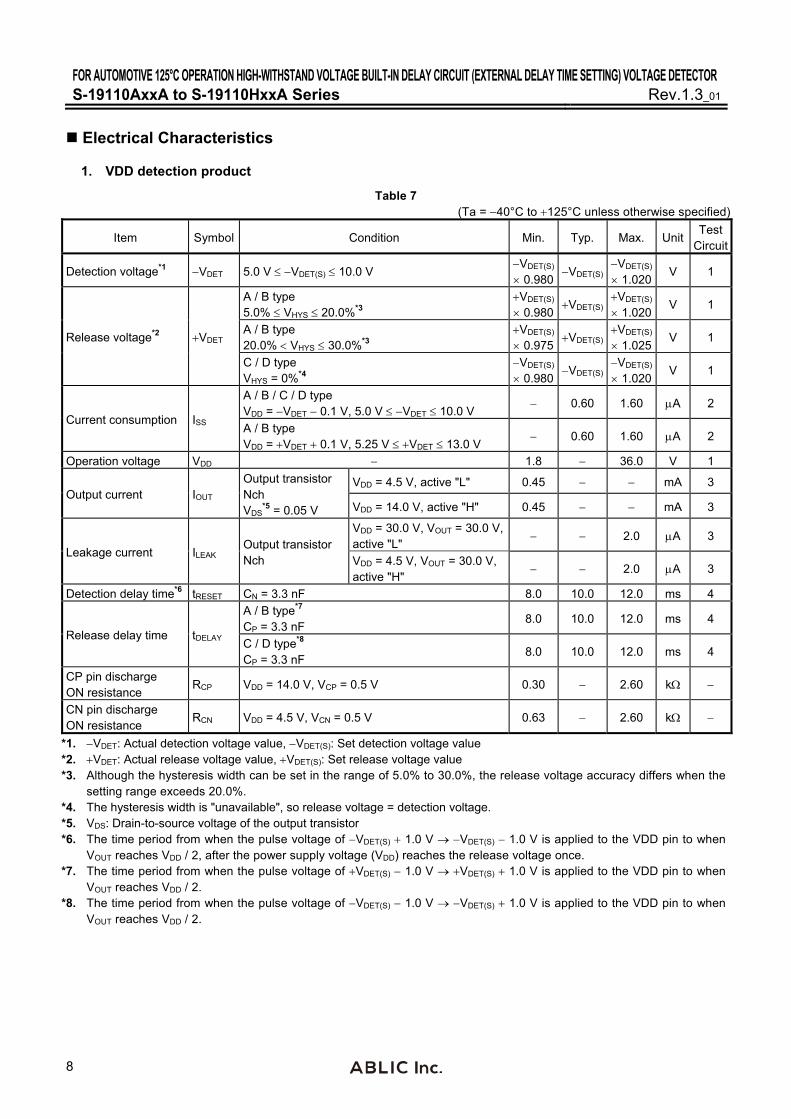
Electrical Characteristics
1. VDD detection product
Table 7 (Ta = 40°C to 125°C unless otherwise specified)
Item Symbol Condition Min. Typ. Max. UnitTest
Circuit
Detection voltage*1 VDET 5.0 V VDET(S) 10.0 V VDET(S) 0.980
VDET(S) VDET(S) 1.020
V 1
Release voltage*2 VDET
A / B type 5.0% VHYS 20.0%*3
VDET(S) 0.980
VDET(S) VDET(S) 1.020
V 1
A / B type 20.0% VHYS 30.0%*3
VDET(S) 0.975
VDET(S) VDET(S) 1.025
V 1
C / D type VHYS = 0%*4
VDET(S) 0.980
VDET(S) VDET(S) 1.020
V 1
Current consumption ISS
A / B / C / D type VDD = VDET 0.1 V, 5.0 V VDET 10.0 V
0.60 1.60 A 2
A / B type VDD = VDET 0.1 V, 5.25 V VDET 13.0 V
0.60 1.60 A 2
Operation voltage VDD 1.8 36.0 V 1
Output current IOUT Output transistor Nch VDS
*5 = 0.05 V
VDD = 4.5 V, active "L" 0.45 mA 3
VDD = 14.0 V, active "H" 0.45 mA 3
Leakage current ILEAK Output transistor Nch
VDD = 30.0 V, VOUT = 30.0 V, active "L"
2.0 A 3
VDD = 4.5 V, VOUT = 30.0 V, active "H"
2.0 A 3
Detection delay time*6 tRESET CN = 3.3 nF 8.0 10.0 12.0 ms 4
Release delay time tDELAY
A / B type*7 CP = 3.3 nF
8.0 10.0 12.0 ms 4
C / D type*8 CP = 3.3 nF
8.0 10.0 12.0 ms 4
CP pin discharge ON resistance
RCP VDD = 14.0 V, VCP = 0.5 V 0.30 2.60 k
CN pin discharge ON resistance
RCN VDD = 4.5 V, VCN = 0.5 V 0.63 2.60 k
*1. VDET: Actual detection voltage value, VDET(S): Set detection voltage value *2. VDET: Actual release voltage value, VDET(S): Set release voltage value *3. Although the hysteresis width can be set in the range of 5.0% to 30.0%, the release voltage accuracy differs when the
setting range exceeds 20.0%. *4. The hysteresis width is "unavailable", so release voltage = detection voltage. *5. VDS: Drain-to-source voltage of the output transistor *6. The time period from when the pulse voltage of VDET(S) 1.0 V VDET(S) 1.0 V is applied to the VDD pin to when
VOUT reaches VDD / 2, after the power supply voltage (VDD) reaches the release voltage once. *7. The time period from when the pulse voltage of VDET(S) 1.0 V VDET(S) 1.0 V is applied to the VDD pin to when
VOUT reaches VDD / 2. *8. The time period from when the pulse voltage of VDET(S) 1.0 V VDET(S) 1.0 V is applied to the VDD pin to when
VOUT reaches VDD / 2.

FOR AUTOMOTIVE 125°C OPERATION HIGH-WITHSTAND VOLTAGE BUILT-IN DELAY CIRCUIT (EXTERNAL DELAY TIME SETTING) VOLTAGE DETECTORRev.1.3_01 S-19110AxxA to S-19110HxxA Series
9
2. SENSE detection product
Table 8 (Ta = 40°C to 125°C unless otherwise specified)
Item Symbol Condition Min. Typ. Max. UnitTest
Circuit
Detection voltage*1 VDET VDD = 16.0 V, 5.0 V VDET(S) 10.0 V VDET(S) 0.980
VDET(S) VDET(S) 1.020
V 1
Release voltage*2 VDET VDD = 16.0 V
E / F type 5.0% VHYS 20.0%*3
VDET(S) 0.980
VDET(S) VDET(S) 1.020
V 1
E / F type 20.0% VHYS 30.0%*3
VDET(S) 0.975
VDET(S) VDET(S) 1.025
V 1
G / H type VHYS = 0%*4
VDET(S) 0.980
VDET(S) VDET(S) 1.020
V 1
Current consumption*5 ISS
E / F / G / H type VDD = 16.0 V, VSENSE = VDET 0.1 V, 5.0 V VDET 10.0 V
0.55 1.55 A 2
E / F type VDD = 16.0 V, VSENSE = VDET 0.1 V, 5.25 V VDET 13.0 V
0.55 1.55 A 2
Operation voltage VDD 3.0 36.0 V 1
Output current IOUT Output transistor Nch VDS
*6 = 0.05 V
VDD = 5.0 V, VSENSE = 4.5 V, active "L"
0.45 mA 3
VDD = 5.0 V, VSENSE = 14.0 V, active "H"
0.45 mA 3
Leakage current ILEAK Output transistor Nch
VDD = 30.0 V, VOUT = 30.0 V, VSENSE = 30.0 V, active "L"
2.0 A 3
VDD = 30.0 V, VOUT = 30.0 V, VSENSE = 4.5 V, active "H"
2.0 A 3
Detection delay time*7 tRESET CN = 3.3 nF 8.0 10.0 12.0 ms 4
Release delay time tDELAY
E / F type*8 CP = 3.3 nF
8.0 10.0 12.0 ms 4
G / H type*9 CP = 3.3 nF
8.0 10.0 12.0 ms 4
SENSE pin resistance RSENSE 26.0 400 M 2
CP pin discharge ON resistance
RCP VDD = 4.5 V, VSENSE = 14.0 V, VCP = 0.5 V 0.30 2.60 k
CN pin discharge ON resistance
RCN VDD = 4.5 V, VSENSE = 4.5 V, VCN = 0.5 V 0.63 2.60 k
*1. VDET: Actual detection voltage value, VDET(S): Set detection voltage value *2. VDET: Actual release voltage value, VDET(S): Set release voltage value *3. Although the hysteresis width can be set in the range of 5.0% to 30.0%, the release voltage accuracy differs when the
setting range exceeds 20.0%. *4. The hysteresis width is "unavailable", so release voltage = detection voltage. *5. The current flowing through the SENSE pin resistance is not included. *6. VDS: Drain-to-source voltage of the output transistor *7. The time period from when the pulse voltage of VDET(S) 1.0 V VDET(S) 1.0 V is applied to the SENSE pin to
when VOUT reaches VDD / 2, after voltage of 16.0 V is applied to the VDD pin and the SENSE pin input voltage (VSENSE) reaches the release voltage once.
*8. The time period from when voltage of 16.0 V is applied to the VDD pin and the pulse voltage of VDET(S) 1.0 V VDET(S) 1.0 V is applied to the SENSE pin to when VOUT reaches VDD / 2.
*9. The time period from when voltage of 16.0 V is applied to the VDD pin and the pulse voltage of VDET(S) 1.0 V VDET(S) 1.0 V is applied to the SENSE pin to when VOUT reaches VDD / 2.

FOR AUTOMOTIVE 125°C OPERATION HIGH-WITHSTAND VOLTAGE BUILT-IN DELAY CIRCUIT (EXTERNAL DELAY TIME SETTING) VOLTAGE DETECTOR S-19110AxxA to S-19110HxxA Series Rev.1.3_01
10
Test Circuits
VDD
VDD
VSS
OUT
R 100 k
VV
CP CN
VDD
VDD
VSS
OUT
R 100 k
VV
CP CN VSENSE
SENSE
Figure 9 Test Circuit 1 Figure 10 Test Circuit 1 (VDD Detection Product) (SENSE Detection Product)
VDD
VSS
OUT
CP CN
A
VDD
VDD
VSS
OUT
CP CN
A
VDDSENSE
VSENSE
A
Figure 11 Test Circuit 2 Figure 12 Test Circuit 2 (VDD Detection Product) (SENSE Detection Product)
VDD
VSS
OUT
CP CN VDS
A
V V
VDD
VDD
VSS
OUT
CP CN VDS
A
V V
VDD
SENSE VSENSE
Figure 13 Test Circuit 3 Figure 14 Test Circuit 3 (VDD Detection Product) (SENSE Detection Product)
VDD
VSS
OUT
CP CN
R 100 k
OscilloscopeP.G.
VDD
VSS
OUT
CP CN
R 100 k
OscilloscopeP.G.
SENSE
VDD
Figure 15 Test Circuit 4 Figure 16 Test Circuit 4 (VDD Detection Product) (SENSE Detection Product)
FOR AUTOMOTIVE 125°C OPERATION HIGH-WITHSTAND VOLTAGE BUILT-IN DELAY CIRCUIT (EXTERNAL DELAY TIME SETTING) VOLTAGE DETECTORRev.1.3_01 S-19110AxxA to S-19110HxxA Series
11
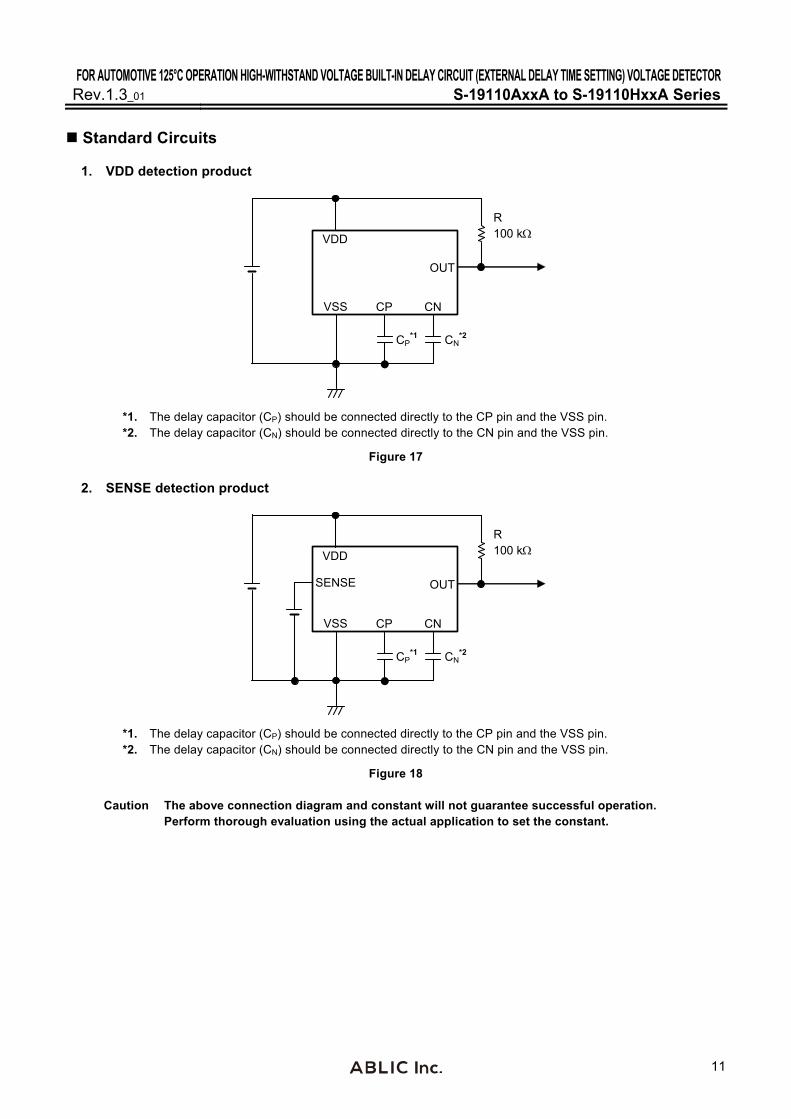
Standard Circuits
1. VDD detection product
VDD
OUT
VSS
R 100 k
CP CN
CN*2CP
*1
*1. The delay capacitor (CP) should be connected directly to the CP pin and the VSS pin. *2. The delay capacitor (CN) should be connected directly to the CN pin and the VSS pin.
Figure 17
2. SENSE detection product
VDD
OUT
VSS
R 100 k
SENSE
CP CN
CN*2CP
*1
*1. The delay capacitor (CP) should be connected directly to the CP pin and the VSS pin. *2. The delay capacitor (CN) should be connected directly to the CN pin and the VSS pin.
Figure 18
Caution The above connection diagram and constant will not guarantee successful operation. Perform thorough evaluation using the actual application to set the constant.

FOR AUTOMOTIVE 125°C OPERATION HIGH-WITHSTAND VOLTAGE BUILT-IN DELAY CIRCUIT (EXTERNAL DELAY TIME SETTING) VOLTAGE DETECTOR S-19110AxxA to S-19110HxxA Series Rev.1.3_01
12
Explanation of Terms
1. Detection voltage (VDET)
The detection voltage is a voltage at which the output in Figure 23 or Figure 24 turns to "H" for active "H", and "L" for active "L" (VDD detection product: VDD, SENSE detection product: VSENSE). The detection voltage varies slightly among products of the same specification. The variation of detection voltage between the specified minimum (VDET min.) and the maximum (VDET max.) is called the detection voltage range (Refer to Figure 19, Figure 21).
Example: In VDET = 5.0 V product, the detection voltage is either one in the range of 4.900 V VDET 5.100 V. This means that some VDET = 5.0 V product have VDET = 4.900 V and some have VDET = 5.100 V.
2. Release voltage (VDET)
The release voltage is a voltage at which the output in Figure 23 or Figure 24 turns to "L" for active "H", and "H" for active "L" (VDD detection product: VDD, SENSE detection product: VSENSE). The difference of detection voltage and release voltage can be set in the range of 5.0% to 30.0% (Refer to "Figure 5 Detection Voltage and Release Voltage Possible Setting Area (VDET 10.0 V)"). The release voltage varies slightly among products of the same specification. The variation of release voltage between the specified minimum (VDET min.) and the maximum (VDET max.) is called the release voltage range (Refer to Figure 20, Figure 22). Release voltage accuracy is 2.0% when hysteresis width = 5.0% to 20.0%, and 2.5% when hysteresis width = 20.0% to 30.0%. In the S-19110 Series C / D / G / H type, the release voltage (VDET) is the same value as the actual detection voltage (VDET) of a product.
Example 1: For VDET = 6.0 V, VDET = 6.6 V product (hysteresis width = 10.0%), the release voltage is either one in the range of 6.468 V VDET 6.732 V.
This means that some VDET = 6.0 V, VDET = 6.6 V product have VDET = 6.468 V and some have VDET = 6.732 V.
Example 2: For VDET = 10.0 V, VDET = 13.0 V product (hysteresis width = 30.0%), the release voltage is either
one in the range of 12.675 V VDET 13.325 V. This means that some VDET = 10.0 V, VDET = 13.0 V product have VDET = 12.675 V and some
have VDET = 13.325 V.

FOR AUTOMOTIVE 125°C OPERATION HIGH-WITHSTAND VOLTAGE BUILT-IN DELAY CIRCUIT (EXTERNAL DELAY TIME SETTING) VOLTAGE DETECTORRev.1.3_01 S-19110AxxA to S-19110HxxA Series
13
Detection voltage
Detection voltage
range
VDD
VDET min.
VDET max.
VOUT
tRESET
VDD
VDET min.
VDET max.
VOUT
Release voltage
Release voltagerange
tDELAY
Figure 19 Detection Voltage (VDD Detection Product) Figure 20 Release Voltage (VDD Detection Product)
Detection voltage
VSENSE
VDET min.
VDET max.
VOUT
tRESET
Detection voltage
range
VSENSE
VDET min.
VDET max.
VOUT
tDELAY
Release voltage
Release voltagerange
Figure 21 Detection Voltage Figure 22 Release Voltage (SENSE Detection Product) (SENSE Detection Product)
VDD
VDD
VSS
OUT
R 100 k
VV
CP CN
VDD
VDD
VSS
OUT
R 100 k
VV
CP CN VSENSE
SENSE
Figure 23 Test Circuit of Detection Voltage Figure 24 Test Circuit of Detection Voltage and Release Voltage and Release Voltage (VDD Detection Product) (SENSE Detection Product)
3. Hysteresis width (VHYS)
The hysteresis width is the voltage difference between the detection voltage and the release voltage (the voltage at point B the voltage at point A = VHYS in Figure 26, Figure 28, Figure 34 and Figure 36). Setting the hysteresis width between the detection voltage and the release voltage, prevents malfunction caused by noise on the input voltage.
4. Feed-through current
The feed-through current is a current that flows instantaneously to the VDD pin at the time of detection and release of a voltage detector.

FOR AUTOMOTIVE 125°C OPERATION HIGH-WITHSTAND VOLTAGE BUILT-IN DELAY CIRCUIT (EXTERNAL DELAY TIME SETTING) VOLTAGE DETECTOR S-19110AxxA to S-19110HxxA Series Rev.1.3_01
14
Operation
1. Basic operation
1. 1 S-19110 Series A type
(1) When the power supply voltage (VDD) is the release voltage (VDET) or higher, the Nch transistor is turned off to output VDD ("H") when the output is pulled up.
Since the Nch transistor (N1) is turned off, the input voltage to the comparator is (RB RC ) VDD
RA RB RC .
(2) Even if VDD decreases to VDET or lower, VDD is output when VDD is higher than the detection voltage (VDET). When VDD decreases to VDET or lower (point A in Figure 26), the Nch transistor is turned on. And then VSS ("L")
is output from the OUT pin after the elapse of the detection delay time (tRESET).
At this time, N1 is turned on, and the input voltage to the comparator is RB VDD
RA RB .
(3) The output is unstable when VDD decreases to the IC's minimum operation voltage or lower. VDD is output when the output is pulled up.
(4) VSS is output by increasing VDD to the minimum operation voltage or higher. Even if VDD exceeds VDET, VSS is output when VDD is lower than VDET.
(5) When VDD increases to VDET or higher (point B in Figure 26), the Nch transistor is turned off. And then VDD is output from the OUT pin after the elapse of the release delay time (tDELAY) when the output is pulled up.
VSS
*1
*1VREF
OUT
VDD
N1
RB
RC
RA
VDD
V
R 100 k
Nch
Delaycircuit
*1
CNCN
*1
CPCP
*1. Parasitic diode
Figure 25 Operation of S-19110 Series A Type
AB
VDD
VSS
Minimum operation voltage
Output from OUT pin
VDD
VSS
(1) (2) (3) (5)(4)
tRESET tDELAY
Hysteresis width
(VHYS) Release voltage (VDET)
Detection voltage (VDET)
Remark When VDD is the minimum operation voltage or lower, the output voltage from the OUT pin is unstable in
the shaded area.
Figure 26 Timing Chart of S-19110 Series A Type

FOR AUTOMOTIVE 125°C OPERATION HIGH-WITHSTAND VOLTAGE BUILT-IN DELAY CIRCUIT (EXTERNAL DELAY TIME SETTING) VOLTAGE DETECTORRev.1.3_01 S-19110AxxA to S-19110HxxA Series
15
1. 2 S-19110 Series B type
(1) When the power supply voltage (VDD) is the release voltage (VDET) or higher, the Nch transistor is turned on to output VSS ("L").
Since the Nch transistor (N1) is turned off, the input voltage to the comparator is (RB RC ) VDD
RA RB RC .
(2) Even if VDD decreases to VDET or lower, VSS is output when VDD is higher than the detection voltage (VDET). When VDD decreases to VDET or lower (point A in Figure 28), the Nch transistor is turned off. And then VDD
("H") is output from the OUT pin after the elapse of the detection delay time (tRESET).
At this time, N1 is turned on, and the input voltage to the comparator is RB VDD
RA RB .
(3) The output is unstable when VDD decreases to the IC's minimum operation voltage or lower. VDD is output when the output is pulled up.
(4) VDD is output by increasing VDD to the minimum operation voltage or higher. Even if VDD exceeds VDET, VDD is output when VDD is lower than VDET.
(5) When VDD increases to VDET or higher (point B in Figure 28), the Nch transistor is turned on. And then VSS is output from the OUT pin after the elapse of the release delay time (tDELAY).
VSS
*1
*1VREF
OUT
VDD
N1
RB
RC
RA
VDD
V
R 100 k
Nch
Delaycircuit
*1
CNCN
*1
CPCP
*1. Parasitic diode
Figure 27 Operation of S-19110 Series B Type
AB
VDD
VSS
VDD
VSS
(1) (2) (3) (5)(4)
tRESET tDELAY
Hysteresis width
(VHYS)
Output from OUT pin
Minimum operation voltage
Release voltage (VDET)
Detection voltage (VDET)
Remark When VDD is the minimum operation voltage or lower, the output voltage from the OUT pin is unstable in
the shaded area.
Figure 28 Timing Chart of S-19110 Series B Type
FOR AUTOMOTIVE 125°C OPERATION HIGH-WITHSTAND VOLTAGE BUILT-IN DELAY CIRCUIT (EXTERNAL DELAY TIME SETTING) VOLTAGE DETECTOR S-19110AxxA to S-19110HxxA Series Rev.1.3_01
16
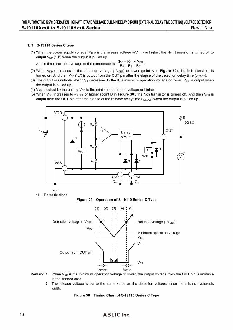
1. 3 S-19110 Series C type
(1) When the power supply voltage (VDD) is the release voltage (VDET) or higher, the Nch transistor is turned off to output VDD ("H") when the output is pulled up.
At this time, the input voltage to the comparator is (RB RC ) VDD
RA RB RC .
(2) When VDD decreases to the detection voltage (VDET) or lower (point A in Figure 30), the Nch transistor is turned on. And then VSS ("L") is output from the OUT pin after the elapse of the detection delay time (tRESET).
(3) The output is unstable when VDD decreases to the IC's minimum operation voltage or lower. VDD is output when the output is pulled up.
(4) VSS is output by increasing VDD to the minimum operation voltage or higher. (5) When VDD increases to VDET or higher (point B in Figure 30), the Nch transistor is turned off. And then VDD is
output from the OUT pin after the elapse of the release delay time (tDELAY) when the output is pulled up.
VSS
*1
*1VREF
OUT
VDD
RB
RC
RA
VDD
V
R 100 k
Nch
Delaycircuit
*1
CNCN
*1
CPCP
*1. Parasitic diode
Figure 29 Operation of S-19110 Series C Type
A B
VDD
VSS
VDD
VSS
(1) (2) (3) (5)(4)
tRESET tDELAY
Output from OUT pin
Minimum operation voltage
Release voltage (VDET) Detection voltage (VDET)
Remark 1. When VDD is the minimum operation voltage or lower, the output voltage from the OUT pin is unstable
in the shaded area. 2. The release voltage is set to the same value as the detection voltage, since there is no hysteresis
width.
Figure 30 Timing Chart of S-19110 Series C Type
FOR AUTOMOTIVE 125°C OPERATION HIGH-WITHSTAND VOLTAGE BUILT-IN DELAY CIRCUIT (EXTERNAL DELAY TIME SETTING) VOLTAGE DETECTORRev.1.3_01 S-19110AxxA to S-19110HxxA Series
17
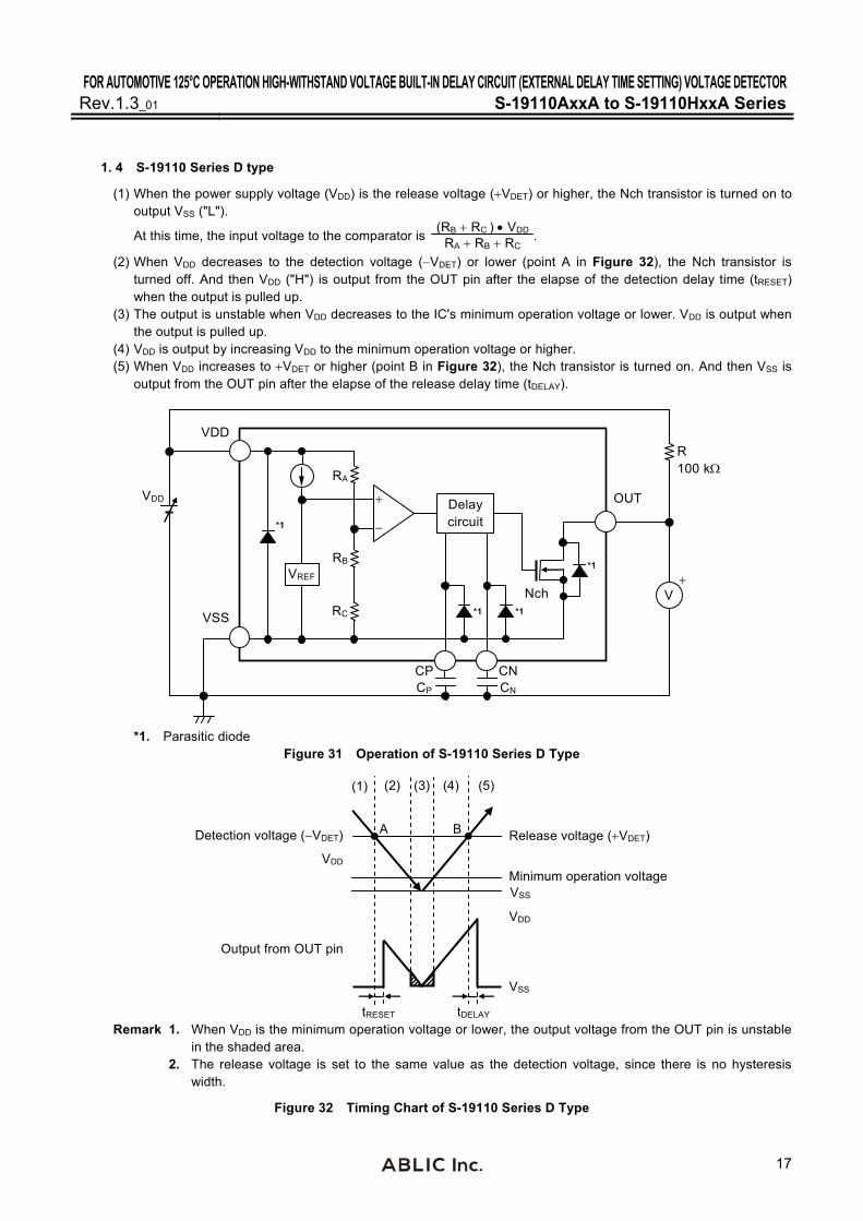
1. 4 S-19110 Series D type
(1) When the power supply voltage (VDD) is the release voltage (VDET) or higher, the Nch transistor is turned on to output VSS ("L").
At this time, the input voltage to the comparator is (RB RC ) VDD
RA RB RC .
(2) When VDD decreases to the detection voltage (VDET) or lower (point A in Figure 32), the Nch transistor is turned off. And then VDD ("H") is output from the OUT pin after the elapse of the detection delay time (tRESET) when the output is pulled up.
(3) The output is unstable when VDD decreases to the IC's minimum operation voltage or lower. VDD is output when the output is pulled up.
(4) VDD is output by increasing VDD to the minimum operation voltage or higher. (5) When VDD increases to VDET or higher (point B in Figure 32), the Nch transistor is turned on. And then VSS is
output from the OUT pin after the elapse of the release delay time (tDELAY).
VSS
*1
*1VREF
OUT
VDD
RB
RC
RA
VDD
V
R 100 k
Nch
Delaycircuit
*1
CNCN
*1
CPCP
*1. Parasitic diode
Figure 31 Operation of S-19110 Series D Type
A B
VDD
VSS
VDD
VSS
(1) (2) (3) (5)(4)
tRESET tDELAY
Output from OUT pin
Minimum operation voltage
Release voltage (VDET) Detection voltage (VDET)
Remark 1. When VDD is the minimum operation voltage or lower, the output voltage from the OUT pin is unstable
in the shaded area. 2. The release voltage is set to the same value as the detection voltage, since there is no hysteresis
width.
Figure 32 Timing Chart of S-19110 Series D Type

FOR AUTOMOTIVE 125°C OPERATION HIGH-WITHSTAND VOLTAGE BUILT-IN DELAY CIRCUIT (EXTERNAL DELAY TIME SETTING) VOLTAGE DETECTOR S-19110AxxA to S-19110HxxA Series Rev.1.3_01
18
1. 5 S-19110 Series E type
(1) When the power supply voltage (VDD) is the minimum operation voltage or higher, and the SENSE pin voltage (VSENSE) is the release voltage (VDET) or higher, the Nch transistor is turned off to output VDD ("H") when the output is pulled up.
Since the Nch transistor (N1) is turned off, the input voltage to the comparator is (RB RC ) VSENSE
RA RB RC .
(2) Even if VSENSE decreases to VDET or lower, VDD is output when VSENSE is higher than the detection voltage (VDET).
When VSENSE decreases to VDET or lower (point A in Figure 34), the Nch transistor is turned on. And then VSS ("L") is output from the OUT pin after the elapse of the detection delay time (tRESET).
At this time, N1 is turned on, and the input voltage to the comparator is RB VSENSE
RA RB .
(3) Even if VSENSE further decreases to the IC's minimum operation voltage or lower, the output from the OUT pin is stable when VDD is minimum operation voltage or higher.
(4) Even if VSENSE exceeds VDET, VSS is output when VSENSE is lower than VDET. (5) When VSENSE increases to VDET or higher (point B in Figure 34), the Nch transistor is turned off. And then VDD
is output from the OUT pin after the elapse of the release delay time (tDELAY) when the output is pulled up.
VSS
*1
*1 VREF
OUT
VDD
*1
SENSE
N1
RB
RC
RA
VDD
V
R 100 k
VSENSE
Nch
Delaycircuit
*1
CNCN
*1
CPCP
*1. Parasitic diode
Figure 33 Operation of S-19110 Series E Type
Hysteresis width
(VHYS) AB
VSENSE
VSS
VDD
VSS
(1) (2) (3) (5)(4)
tRESET tDELAY
Output from OUT pin
Minimum operation voltage
Release voltage (VDET)
Detection voltage (VDET)
Figure 34 Timing Chart of S-19110 Series E Type
FOR AUTOMOTIVE 125°C OPERATION HIGH-WITHSTAND VOLTAGE BUILT-IN DELAY CIRCUIT (EXTERNAL DELAY TIME SETTING) VOLTAGE DETECTORRev.1.3_01 S-19110AxxA to S-19110HxxA Series
19
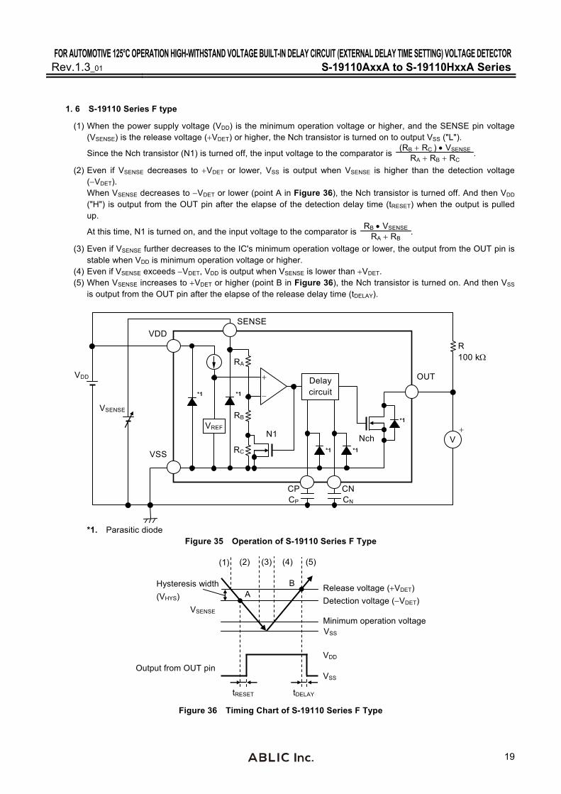
1. 6 S-19110 Series F type
(1) When the power supply voltage (VDD) is the minimum operation voltage or higher, and the SENSE pin voltage (VSENSE) is the release voltage (VDET) or higher, the Nch transistor is turned on to output VSS ("L").
Since the Nch transistor (N1) is turned off, the input voltage to the comparator is (RB RC ) VSENSE
RA RB RC .
(2) Even if VSENSE decreases to VDET or lower, VSS is output when VSENSE is higher than the detection voltage (VDET).
When VSENSE decreases to VDET or lower (point A in Figure 36), the Nch transistor is turned off. And then VDD ("H") is output from the OUT pin after the elapse of the detection delay time (tRESET) when the output is pulled up.
At this time, N1 is turned on, and the input voltage to the comparator is RB VSENSE
RA RB .
(3) Even if VSENSE further decreases to the IC's minimum operation voltage or lower, the output from the OUT pin is stable when VDD is minimum operation voltage or higher.
(4) Even if VSENSE exceeds VDET, VDD is output when VSENSE is lower than VDET. (5) When VSENSE increases to VDET or higher (point B in Figure 36), the Nch transistor is turned on. And then VSS
is output from the OUT pin after the elapse of the release delay time (tDELAY).
VSS
*1
*1 VREF
OUT
VDD
*1
SENSE
N1
RB
RC
RA
VDD
V
R 100 k
VSENSE
Nch
Delaycircuit
*1
CNCN
*1
CPCP
*1. Parasitic diode
Figure 35 Operation of S-19110 Series F Type
Hysteresis width
(VHYS) AB
VSENSE
VSS
VDD
VSS
(1) (2) (3) (5)(4)
tRESET tDELAY
Output from OUT pin
Minimum operation voltage
Release voltage (VDET)
Detection voltage (VDET)
Figure 36 Timing Chart of S-19110 Series F Type

FOR AUTOMOTIVE 125°C OPERATION HIGH-WITHSTAND VOLTAGE BUILT-IN DELAY CIRCUIT (EXTERNAL DELAY TIME SETTING) VOLTAGE DETECTOR S-19110AxxA to S-19110HxxA Series Rev.1.3_01
20
1. 7 S-19110 Series G type
(1) When the power supply voltage (VDD) is the minimum operation voltage or higher, and the SENSE pin voltage (VSENSE) is the release voltage (VDET) or higher, the Nch transistor is turned off to output VDD ("H") when the output is pulled up.
At this time, the input voltage to the comparator is (RB RC ) VSENSE
RA RB RC .
(2) When VSENSE decreases to the detection voltage (VDET) or lower (point A in Figure 38), the Nch transistor is turned on. And then VSS ("L") is output from the OUT pin after the elapse of the detection delay time (tRESET).
(3) Even if VSENSE further decreases to the IC's minimum operation voltage or lower, the output from the OUT pin is stable when VDD is minimum operation voltage or higher.
(4) Even if VSENSE increases, VSS is output when VSENSE is lower than VDET. (5) When VSENSE increases to VDET or higher (point B in Figure 38), the Nch transistor is turned off. And then VDD
is output from the OUT pin after the elapse of the release delay time (tDELAY) when the output is pulled up.
VSS
*1
*1 VREF
OUT
VDD
*1
SENSE
RB
RC
RA
VDD
V
R 100 k
VSENSE
Nch
Delaycircuit
*1
CNCN
*1
CPCP
*1. Parasitic diode
Figure 37 Operation of S-19110 Series G Type
A B
VSENSE
VSS
VDD
VSS
(1) (2) (3) (5)(4)
tRESET tDELAY
Output from OUT pin
Minimum operation voltage
Detection voltage (VDET) Release voltage (VDET)
Remark The release voltage is set to the same value as the detection voltage, since there is no hysteresis width.
Figure 38 Timing Chart of S-19110 Series G Type

FOR AUTOMOTIVE 125°C OPERATION HIGH-WITHSTAND VOLTAGE BUILT-IN DELAY CIRCUIT (EXTERNAL DELAY TIME SETTING) VOLTAGE DETECTORRev.1.3_01 S-19110AxxA to S-19110HxxA Series
21
1. 8 S-19110 Series H type
(1) When the power supply voltage (VDD) is the minimum operation voltage or higher, and the SENSE pin voltage (VSENSE) is the release voltage (VDET) or higher, the Nch transistor is turned on to output VSS ("L").
At this time, the input voltage to the comparator is (RB RC ) VSENSE
RA RB RC .
(2) When VSENSE decreases to the detection voltage (VDET) or lower (point A in Figure 40), the Nch transistor is turned off. And then VDD ("H") is output from the OUT pin after the elapse of the detection delay time (tRESET) when the output is pulled up.
(3) Even if VSENSE further decreases to the IC's minimum operation voltage or lower, the output from the OUT pin is stable when VDD is minimum operation voltage or higher.
(4) Even if VSENSE increases, VDD is output when VSENSE is lower than VDET. (5) When VSENSE increases to VDET or higher (point B in Figure 40), the Nch transistor is turned on. And then VSS
is output from the OUT pin after the elapse of the release delay time (tDELAY).
VSS
*1
*1 VREF
OUT
VDD
*1
SENSE
RB
RC
RA
VDD
V
R 100 k
VSENSE
Nch
Delaycircuit
*1
CNCN
*1
CPCP
*1. Parasitic diode
Figure 39 Operation of S-19110 Series H Type
A B
VSENSE
VSS
VDD
VSS
(1) (2) (3) (5)(4)
tRESET tDELAY
Output from OUT pin
Minimum operation voltage
Detection voltage (VDET) Release voltage (VDET)
Remark The release voltage is set to the same value as the detection voltage, since there is no hysteresis width.
Figure 40 Timing Chart of S-19110 Series H Type

FOR AUTOMOTIVE 125°C OPERATION HIGH-WITHSTAND VOLTAGE BUILT-IN DELAY CIRCUIT (EXTERNAL DELAY TIME SETTING) VOLTAGE DETECTOR S-19110AxxA to S-19110HxxA Series Rev.1.3_01
22
2. SENSE pin
2. 1 Error when detection voltage is set externally
The detection voltage for the S-19110 Series is 10.0 V max., however, in the SENSE detection product with VDET = 10.0 V, the detection voltage can be set externally by connecting a node that was resistance-divided by the resistor (RA) and the resistor (RB) to the SENSE pin as shown in Figure 41. For conventional products without the SENSE pin, external resistor cannot be too large since the resistance-divided node must be connected to the VDD pin. This is because a feed-through current will flow through the VDD pin when it goes from detection to release, and if external resistor is large, problems such as oscillation or larger error in the hysteresis width may occur. In the S-19110 Series, RA and RB in Figure 41 are easily made larger since the resistance-divided node can be connected to the SENSE pin through which no feed-through current flows. However, be careful of error in the current flowing through the internal resistance (RSENSE) that will occur. Although RSENSE in the S-19110 Series is large (26 M min.) to make the error small, RA and RB should be selected such that the error is within the allowable limits.
2. 2 Selection of RA and RB
In Figure 41, the relation between the external setting detection voltage (VDX) and the actual detection voltage (VDET) is ideally calculated by the equation below.
VDX = VDET ( )1 RA
RB ··· (1)
However, in reality there is an error in the current flowing through RSENSE. When considering this error, the relation between VDX and VDET is calculated as follows.
VDX = VDET ( )1 RA
RB || RSENSE
= VDET
1
RA
RB RSENSE
RB RSENSE
= VDET ( )1 RA
RB
RA
RSENSE VDET ··· (2)
By using equations (1) and (2), the error is calculated as VDET RA
RSENSE .
The error rate is calculated as follows by dividing the error by the right-hand side of equation (1).
RA RB
RSENSE (RA RB) 100 [%] = RA || RB
RSENSE 100 [%] ··· (3)
As seen in equation (3), the smaller the resistance values of RA and RB compared to RSENSE, the smaller the error rate becomes.

FOR AUTOMOTIVE 125°C OPERATION HIGH-WITHSTAND VOLTAGE BUILT-IN DELAY CIRCUIT (EXTERNAL DELAY TIME SETTING) VOLTAGE DETECTORRev.1.3_01 S-19110AxxA to S-19110HxxA Series
23
Also, the relation between the external setting hysteresis width (VHX) and the hysteresis width (VHYS) is calculated by equation below. Error due to RSENSE also occurs to the relation in a similar way to the detection voltage.
VHX = VHYS ( )1 RA
RB ··· (4)
VSS
OUT
VDD
SENSE
RA
RB
VDX VDET
RSENSE
A
Figure 41 Detection Voltage External Setting Circuit
Caution 1. When externally setting the detection voltage, perform the operation with VDET = 10.0 V
product. Contact our sales office for details.
2. If the current flowing through RB is set to 1 A or less, the error may become larger.
3. If the parasitic resistance and parasitic inductance between VDX point A and point A VDD
pin are larger, oscillation may occur. Perform thorough evaluation using the actual
application.
4. If RA and RB are large, the SENSE pin input impedance becomes higher and may cause a
malfunction due to noise. In this case, connect a capacitor between the SENSE pin and the
VSS pin.

FOR AUTOMOTIVE 125°C OPERATION HIGH-WITHSTAND VOLTAGE BUILT-IN DELAY CIRCUIT (EXTERNAL DELAY TIME SETTING) VOLTAGE DETECTOR S-19110AxxA to S-19110HxxA Series Rev.1.3_01
24
3. Delay circuit
The delay circuit has a function that adjusts the detection delay time (tRESET) from when the power supply voltage
(VDD) or SENSE pin voltage (VSENSE) reaches the detection voltage (VDET) or lower to when the output from OUT
pin inverts.
It also has a function that adjusts the release delay time (tDELAY) from when the power supply voltage (VDD) or
SENSE pin voltage (VSENSE) reaches the release voltage (VDET) to when the output from OUT pin inverts.
tRESET is determined by the delay coefficient, the delay capacitor (CN) and the detection delay time when the CN pin
is open (tRESET0), and the tDELAY is determined by the delay coefficient, the delay capacitor (CP) and the release
delay time when the CP pin is open (tDELAY0). They are calculated by the equation below.
tRESET [ms] = Delay coefficient CN [nF] tRESET0 [ms] tDELAY [ms] = Delay coefficient CP [nF] tDELAY0 [ms]
Table 9
Operation Temperature
Delay Coefficient
Min. Typ. Max.
Ta = 125°C 2.41 2.85 3.32
Ta = 105°C 2.41 2.85 3.32
Ta = 25°C 2.41 2.86 3.30
Ta = 40°C 2.40 2.83 3.25
Table 10
Operation Temperature
Detection Delay Time when CN Pin is Open (tRESET0)
Release Delay Time when CP Pin is Open (tDELAY0)
Typ. Typ.
Ta = 40°C to 125°C 0.35 ms 0.35 ms
Caution 1. Mounted board layout should be made in such a way that no current flows into or flows from
the CN pin or CP pin since the impedance of the CN pin and CP pin are high, otherwise correct
delay time cannot be provided.
2. There is no limit for the capacitance of CN and CP as long as the leakage current of the
capacitor can be ignored against the built-in constant current value (approximately 300 nA).
The leakage current may cause error in delay time. When the leakage current is larger than the
built-in constant current, no detect or release takes place.
3. The above equation will not guarantee successful operation. Determine the capacitance of CN
and CP through thorough evaluation including temperature characteristics in the actual usage
conditions.
When using an X8R equivalent capacitor, refer to the "2. Detection delay time (tRESET) vs.
Temperature (Ta)", "3. Detection delay time (tRESET) vs. Power supply voltage (VDD)", "5.
Release delay time (tDELAY) vs. Temperature (Ta)" and "6. Release delay time (tDELAY) vs.
Power supply voltage (VDD)" in " Reference Data" for details.
FOR AUTOMOTIVE 125°C OPERATION HIGH-WITHSTAND VOLTAGE BUILT-IN DELAY CIRCUIT (EXTERNAL DELAY TIME SETTING) VOLTAGE DETECTORRev.1.3_01 S-19110AxxA to S-19110HxxA Series
25
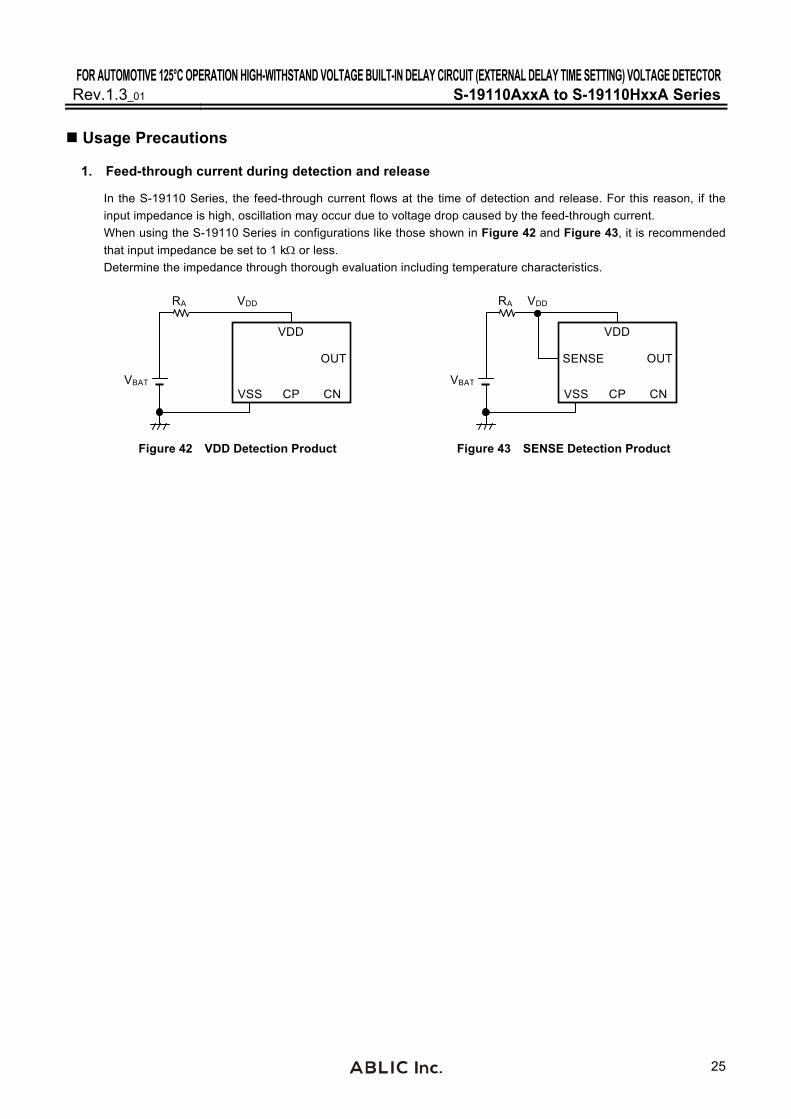
Usage Precautions
1. Feed-through current during detection and release
In the S-19110 Series, the feed-through current flows at the time of detection and release. For this reason, if the
input impedance is high, oscillation may occur due to voltage drop caused by the feed-through current.
When using the S-19110 Series in configurations like those shown in Figure 42 and Figure 43, it is recommended
that input impedance be set to 1 k or less.
Determine the impedance through thorough evaluation including temperature characteristics.
VSS
OUT
VDD
RA
VBAT CNCP
VDD
VSS
OUT
VDD
SENSE
RA
VBAT
CNCP
VDD
Figure 42 VDD Detection Product Figure 43 SENSE Detection Product
FOR AUTOMOTIVE 125°C OPERATION HIGH-WITHSTAND VOLTAGE BUILT-IN DELAY CIRCUIT (EXTERNAL DELAY TIME SETTING) VOLTAGE DETECTOR S-19110AxxA to S-19110HxxA Series Rev.1.3_01
26
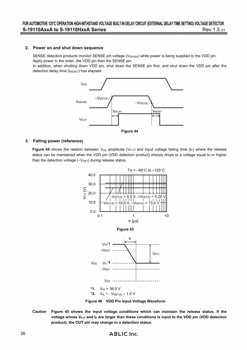
2. Power on and shut down sequence
SENSE detection products monitor SENSE pin voltage (VSENSE) while power is being supplied to the VDD pin. Apply power in the order, the VDD pin then the SENSE pin. In addition, when shutting down VDD pin, shut down the SENSE pin first, and shut down the VDD pin after the detection delay time (tRESET) has elapsed.
VDD
VSENSE
VOUT
VDET(S)
VDET(S)
tDELAY tRESET
Figure 44
3. Falling power (reference)
Figure 45 shows the relation between VDD amplitude (VP-P) and input voltage falling time (tF) where the release
status can be maintained when the VDD pin (VDD detection product) sharply drops to a voltage equal to or higher
than the detection voltage (VDET) during release status. Ta = 40C to 125C
0.1
VP
-P [V
]
0.0
tF [μs]
40.0
30.0
20.0
10.0
101
−VDET(S) = 5.0 V, +VDET(S) = 5.25 V
−VDET(S) = 10.0 V, +VDET(S) = 13.0 V
Figure 45
VIH*1
VDD VIL*2
VDET
VDET
VSS
tF
VP-P
*1. VIH = 36.0 V *2. VIL = VDET(S) 1.0 V
Figure 46 VDD Pin Input Voltage Waveform
Caution Figure 45 shows the input voltage conditions which can maintain the release status. If the
voltage whose VP-P and tF are larger than these conditions is input to the VDD pin (VDD detection
product), the OUT pin may change to a detection status.

FOR AUTOMOTIVE 125°C OPERATION HIGH-WITHSTAND VOLTAGE BUILT-IN DELAY CIRCUIT (EXTERNAL DELAY TIME SETTING) VOLTAGE DETECTORRev.1.3_01 S-19110AxxA to S-19110HxxA Series
27
4. VDD pin, SENSE pin voltage glitch (reference)
4. 1 Detection operation
Figure 47 and Figure 48 show the relation between pulse width and pulse voltage difference (VOD) where the release status can be maintained when a pulse equal to or lower than the detection voltage (VDET) is input to the VDD pin (VDD detection product) or SENSE pin (SENSE detection product) during release status.
Ta = 40C to 125C Ta = 40C to 125C
10
Pul
se w
idth
[s]
0
VOD [mV]
200
150
100
50
1000100
10P
ulse
wid
th [
s]
0
VOD [mV]
1000
750
500
250
1000100
Figure 47 VDD Detection Product Figure 48 SENSE Detection Product
VIH*1
VDD, VSENSE
VIL*2
VDET
VOD
Pulse width
*1. VIH = 16.0 V *2. VIL = VDET VOD
Figure 49 VDD Pin, SENSE Pin Input Voltage Waveform
Caution Figure 47 and Figure 48 show the pulse conditions which can maintain the release status. If the
pulse whose pulse width and VOD are larger than these conditions is input to the VDD pin (VDD
detection product) or SENSE pin (SENSE detection product), the OUT pin may change to a
detection status.

FOR AUTOMOTIVE 125°C OPERATION HIGH-WITHSTAND VOLTAGE BUILT-IN DELAY CIRCUIT (EXTERNAL DELAY TIME SETTING) VOLTAGE DETECTOR S-19110AxxA to S-19110HxxA Series Rev.1.3_01
28
4. 2 Release operation
Figure 50 and Figure 51 show the relation between pulse width and pulse voltage difference (VOD) where the detection status can be maintained when a pulse equal to or higher than the release voltage (VDET) is input to the VDD pin (VDD detection product) or SENSE pin (SENSE detection product) during detection status.
Ta = 40C to 125C Ta = 40C to 125C
10
Pul
se w
idth
[s]
0
VOD [mV]
200
150
100
50
1000100
10
Pul
se w
idth
[s]
0
VOD [mV]
1000
750
500
250
1000100
Figure 50 VDD Detection Product Figure 51 SENSE Detection Product
VIH*1
VDD, VSENSE
VIL*2
VDET
VOD
Pulse width
*1. VIH = VDET VOD *2. VIL = VDET 1.0 V
Figure 52 VDD Pin, SENSE Pin Input Voltage Waveform
Caution Figure 50 and Figure 51 show the pulse conditions which can maintain the detection status. If the
pulse whose pulse width and VOD are larger than these conditions is input to the VDD pin (VDD
detection product) or SENSE pin (SENSE detection product), the OUT pin may change to a
release status.

FOR AUTOMOTIVE 125°C OPERATION HIGH-WITHSTAND VOLTAGE BUILT-IN DELAY CIRCUIT (EXTERNAL DELAY TIME SETTING) VOLTAGE DETECTORRev.1.3_01 S-19110AxxA to S-19110HxxA Series
29
5. Detection delay time accuracy (reference)
Figure 53 and Figure 54 show the relation between VDD amplitude (VP-P) and input voltage falling time (tF) where
the arbitrarily set detection delay time accuracy can be maintained when the VDD pin (VDD detection product)
sharply drops. Ta = 40C to 125C Ta = 40C to 125C
0.1
VP
-P [V
]
0.0
40.0
30.0
20.0
10.0
101tF [μs]
−VDET(S) = 5.0 V, +VDET(S) = 5.25 V
−VDET(S) = 10.0 V, +VDET(S) = 13.0 V
0.1
VP
-P [V
]
0.0
40.0
30.0
20.0
10.0
101tF [μs]
−VDET(S) = 5.0 V, +VDET(S) = 5.25 V
−VDET(S) = 10.0 V, +VDET(S) = 13.0 V
Figure 53 CN = 3.3 nF Figure 54 CN = 100 nF
VIH*1
VDD
VIL*2
VDET
VDET
3.0 VVSS
tF
VP-P
*1. VIH = 36.0 V *2. VIL = VDET(S) 1.0 V (3.0 V min.)
Figure 55 VDD Pin Input Voltage Waveform
Caution Figure 53 and Figure 54 show the input voltage conditions which can maintain the detection
delay time accuracy. If the voltage whose VP-P and tF are larger than these conditions is input to
the VDD pin (VDD detection product), the desired detection delay time may not be achieved.

FOR AUTOMOTIVE 125°C OPERATION HIGH-WITHSTAND VOLTAGE BUILT-IN DELAY CIRCUIT (EXTERNAL DELAY TIME SETTING) VOLTAGE DETECTOR S-19110AxxA to S-19110HxxA Series Rev.1.3_01
30
6. VDD drop during release delay time (reference)
Figure 56 and Figure 57 show the relation between pulse width (tPW) and VDD lower limit (VDROP) where a release
signal can be output after the normal release delay time has elapsed when the VDD pin (VDD detection product)
instantaneously drops to the detection voltage (VDET) or lower and then increases to the release voltage (VDET) or
higher during release delay time. Ta = 40C to 125C, CP = CN = 3.3 nF, Ta = 40C to 125C, CP = CN = 3.3 nF, VDET(S) = 5.0 V, VDET(S) = 5.25 V VDET(S) = 10.0 V, VDET(S) = 10.5 V
0.0
tPW
[s]
1
VDROP [V]
10000
1000
2.00.5 1.51.0
10
100 Inhibited Area
0.0tP
W [
s]
1
VDROP [V]
10000
1000
2.00.5 1.51.0
10
100 Inhibited Area
Figure 56 Figure 57
VDDVDET(S)
VDROP
16 V
VOUT
tF*1 tR*1 tPW
tDELAYtDELAY 0.8
*1. tR = tF = 10 s
Figure 58 VDD Pin Input Voltage Waveform
Caution 1. Figure 56 and Figure 57 show the input voltage conditions when a release signal is output
after the normal release delay time has elapsed. When this is within the inhibited area, release
may erroneously be executed before the delay time completes.
2. When the VDD pin voltage is within the inhibited areas shown in Figure 56 and Figure 57
during release delay time, input 0 V to the VDD pin then restart the S-19110 Series.

FOR AUTOMOTIVE 125°C OPERATION HIGH-WITHSTAND VOLTAGE BUILT-IN DELAY CIRCUIT (EXTERNAL DELAY TIME SETTING) VOLTAGE DETECTORRev.1.3_01 S-19110AxxA to S-19110HxxA Series
31
Precautions
Do not apply an electrostatic discharge to this IC that exceeds the performance ratings of the built-in electrostatic protection circuit.
Because the SENSE pin has a high impedance, malfunctions may occur due to noise. Be careful of wiring adjoining SENSE pin wiring in actual applications. When designing for mass production using an application circuit described herein, the product deviation and
temperature characteristics of the external parts should be taken into consideration. ABLIC Inc. shall not bear any responsibility for patent infringements related to products using the circuits described herein.
ABLIC Inc. claims no responsibility for any disputes arising out of or in connection with any infringement by
products including this IC of patents owned by a third party.

FOR AUTOMOTIVE 125°C OPERATION HIGH-WITHSTAND VOLTAGE BUILT-IN DELAY CIRCUIT (EXTERNAL DELAY TIME SETTING) VOLTAGE DETECTOR S-19110AxxA to S-19110HxxA Series Rev.1.3_01
32
Characteristics (Typical Data)
1. Detection voltage (VDET), Release voltage (VDET) vs. Temperature (Ta)
1. 1 VDD detection product
VDET(S) = 5.0 V, VDET(S) = 5.25 V
4.90
5.40
5.30
Ta [C]
VD
ET,
V
DE
T [V
]
5.20
5.10
5.00
40 25 0 25 50 75 100 125
VDET
VDET
VDET(S) = 7.5 V, VDET(S) = 8.5 V
7.00
9.00
Ta [C]
VD
ET,
V
DE
T [V
]
8.50
8.00
7.50
40 25 0 25 50 75 100 125
VDET
VDET
VDET(S) = 10.0 V, VDET(S) = 13.0 V
Ta [C]40 25 0 25 50 75 100 125
9.00
14.00
13.00
12.00
11.00
10.00VD
ET,
V
DE
T [V
] VDET
VDET
1. 2 SENSE detection product
VDET(S) = 5.0 V, VDET(S) = 5.25 V, VDD = 16.0 V
4.90
5.40
5.30
Ta [C]
VD
ET,
V
DE
T [V
]
5.20
5.10
5.00
40 25 0 25 50 75 100 125
VDET
VDET
VDET(S) = 7.5 V, VDET(S) = 8.5 V, VDD = 16.0 V
7.00
9.00
Ta [C]
VD
ET,
V
DE
T [V
]
8.50
8.00
7.50
40 25 0 25 50 75 100 125
VDET
VDET
VDET(S) = 10.0 V, VDET(S) = 13.0 V, VDD = 16.0 V
Ta [C]40 25 0 25 50 75 100 125
9.00
14.00
13.00
12.00
11.00
10.00VD
ET,
V
DE
T [V
] VDET
VDET
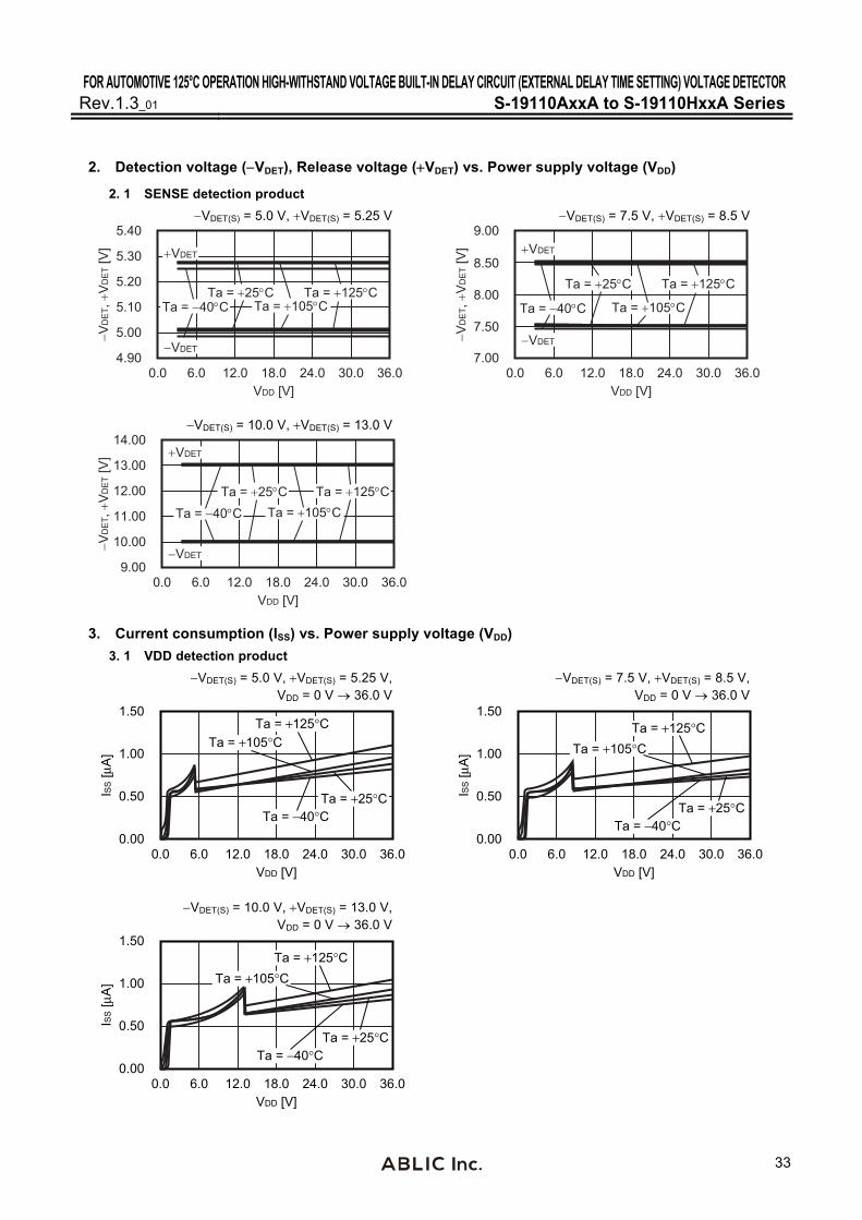
FOR AUTOMOTIVE 125°C OPERATION HIGH-WITHSTAND VOLTAGE BUILT-IN DELAY CIRCUIT (EXTERNAL DELAY TIME SETTING) VOLTAGE DETECTORRev.1.3_01 S-19110AxxA to S-19110HxxA Series
33
2. Detection voltage (VDET), Release voltage (VDET) vs. Power supply voltage (VDD)
2. 1 SENSE detection product
VDET(S) = 5.0 V, VDET(S) = 5.25 V 5.40
4.900.0 36.0
VDD [V]30.024.018.012.06.0
5.30
5.20
5.10
5.00VD
ET,
V
DE
T [V
] VDET
VDET
Ta = 105CTa = 125CTa = 25C
Ta = 40C
VDET(S) = 7.5 V, VDET(S) = 8.5 V 9.00
7.000.0 36.0
VDD [V]30.024.018.012.06.0
VD
ET,
V
DE
T [V
]
8.50
8.00
7.50
VDET
VDET
Ta = 105C
Ta = 125CTa = 25C
Ta = 40C
VDET(S) = 10.0 V, VDET(S) = 13.0 V
14.00
13.00
9.000.0 36.0
VDD [V]30.024.018.012.06.0
VD
ET,
V
DE
T [V
]
12.00
11.00
10.00
VDET
VDET
Ta = 105CTa = 125CTa = 25C
Ta = 40C
3. Current consumption (ISS) vs. Power supply voltage (VDD)
3. 1 VDD detection product
VDET(S) = 5.0 V, VDET(S) = 5.25 V, VDD = 0 V 36.0 V
0.00.00
36.0
ISS [μ
A]
VDD [V]
1.50
30.024.018.012.06.0
1.00
0.50Ta = −40°C
Ta = +25°C
Ta = +105°CTa = +125°C
VDET(S) = 7.5 V, VDET(S) = 8.5 V, VDD = 0 V 36.0 V
0.00.00
36.0
ISS [μ
A]
VDD [V]
1.50
30.024.018.012.06.0
1.00
0.50
Ta = −40°CTa = +25°C
Ta = +105°CTa = +125°C
VDET(S) = 10.0 V, VDET(S) = 13.0 V, VDD = 0 V 36.0 V
0.00.00
36.0
ISS [μ
A]
VDD [V]
1.50
30.024.018.012.06.0
1.00
0.50
Ta = −40°CTa = +25°C
Ta = +105°CTa = +125°C
FOR AUTOMOTIVE 125°C OPERATION HIGH-WITHSTAND VOLTAGE BUILT-IN DELAY CIRCUIT (EXTERNAL DELAY TIME SETTING) VOLTAGE DETECTOR S-19110AxxA to S-19110HxxA Series Rev.1.3_01
34
3. 2 SENSE detection product
VDET(S) = 5.0 V, VDET(S) = 5.25 V, VDD = 0 V 36.0 V, VSENSE = VDET 0.1 V (during detection)
0.00.00
36.0
ISS [
A]
VDD [V]
1.50
30.024.018.012.06.0
1.00
0.50
Ta = 40C
Ta = 25C
Ta = 105C
Ta = 125C
VDET(S) = 5.0 V, VDET(S) = 5.25 V, VDD = 0 V 36.0 V, VSENSE = VDET 0.1 V (during release)
0.00.00
36.0
ISS [
A]
VDD [V]
1.50
30.024.018.012.06.0
1.00
0.50
Ta = 40C
Ta = 25C
Ta = 105C
Ta = 125C
VDET(S) = 7.5 V, VDET(S) = 8.5 V, VDD = 0 V 36.0 V, VSENSE = VDET 0.1 V (during detection)
0.00.00
36.0
ISS [
A]
VDD [V]
1.50
30.024.018.012.06.0
1.00
0.50
Ta = 40C
Ta = 25C
Ta = 105C
Ta = 125C
VDET(S) = 7.5 V, VDET(S) = 8.5 V, VDD = 0 V 36.0 V, VSENSE = VDET 0.1 V (during release)
0.00.00
36.0
ISS [
A]
VDD [V]
1.50
30.024.018.012.06.0
1.00
0.50
Ta = 40C
Ta = 25C
Ta = 105C
Ta = 125C
VDET(S) = 10.0 V, VDET(S) = 13.0 V, VDD = 0 V 36.0 V, VSENSE = VDET 0.1 V (during detection)
0.00.00
36.0
ISS [
A]
VDD [V]
1.50
30.024.018.012.06.0
1.00
0.50
Ta = 40C
Ta = 25C
Ta = 105C
Ta = 125C
VDET(S) = 10.0 V, VDET(S) = 13.0 V, VDD = 0 V 36.0 V, VSENSE = VDET 0.1 V (during release)
0.00.00
36.0
ISS [
A]
VDD [V]
1.50
30.024.018.012.06.0
1.00
0.50
Ta = 40C
Ta = 25C
Ta = 105C
Ta = 125C
FOR AUTOMOTIVE 125°C OPERATION HIGH-WITHSTAND VOLTAGE BUILT-IN DELAY CIRCUIT (EXTERNAL DELAY TIME SETTING) VOLTAGE DETECTORRev.1.3_01 S-19110AxxA to S-19110HxxA Series
35
4. Current consumption (ISS) vs. Temperature (Ta)
4. 1 VDD detection product
VDET(S) = 5.0 V, VDET(S) = 5.25 V, VDD = VDET 0.1 V
Ta [C]40 25 0 25 50 75 100 125
0.00
1.50
1.00
0.50ISS [
A]
VDET(S) = 7.5 V, VDET(S) = 8.5 V, VDD = VDET 0.1 V
Ta [C]40 25 0 25 50 75 100 125
0.00
1.50
1.00
0.50ISS [
A]
VDET(S) = 10.0 V, VDET(S) = 13.0 V, VDD = VDET 0.1 V
Ta [C]40 25 0 25 50 75 100 125
0.00
1.50
1.00
0.50ISS [
A]
4. 2 SENSE detection product
VDET(S) = 5.0 V, VDET(S) = 5.25 V, VDD = 16.0 V, VSENSE = VDET 0.1 V
Ta [C]40 25 0 25 50 75 100 125
0.00
1.50
1.00
0.50ISS [
A]
VDET(S) = 7.5 V, VDET(S) = 8.5 V, VDD = 16.0 V, VSENSE = VDET 0.1 V
Ta [C]40 25 0 25 50 75 100 125
0.00
1.50
1.00
0.50ISS [
A]
VDET(S) = 10.0 V, VDET(S) = 13.0 V, VDD = 16.0 V, VSENSE = VDET 0.1 V
Ta [C]40 25 0 25 50 75 100 125
0.00
1.50
1.00
0.50ISS [
A]

FOR AUTOMOTIVE 125°C OPERATION HIGH-WITHSTAND VOLTAGE BUILT-IN DELAY CIRCUIT (EXTERNAL DELAY TIME SETTING) VOLTAGE DETECTOR S-19110AxxA to S-19110HxxA Series Rev.1.3_01
36
5. Current consumption during detection delay (ISS) vs. Temperature (Ta)
5. 1 VDD detection product 5. 2 SENSE detection product
VDET(S) = 7.5 V, VDET(S) = 8.5 V, VCN = 0.2 V
Ta [°C]40 25 0 25 50 75 100 125
0.00
3.00
2.00
1.00ISS [μ
A]
VDET(S) = 7.5 V, VDET(S) = 8.5 V, VDD = 16.0 V, VCN = 0.2 V
Ta [°C]40 25 0 25 50 75 100 125
0.00
3.00
2.00
1.00ISS [μ
A]
6. Current consumption during release delay (ISS) vs. Temperature (Ta)
6. 1 VDD detection product 6. 2 SENSE detection product
VDET(S) = 7.5 V, VDET(S) = 8.5 V, VCP = 0.2 V
Ta [°C]40 25 0 25 50 75 100 125
0.00
3.00
2.00
1.00ISS [μ
A]
VDET(S) = 7.5 V, VDET(S) = 8.5 V, VDD = 16.0 V, VCP = 0.2 V
Ta [°C]40 25 0 25 50 75 100 125
0.00
3.00
2.00
1.00ISS [μ
A]

FOR AUTOMOTIVE 125°C OPERATION HIGH-WITHSTAND VOLTAGE BUILT-IN DELAY CIRCUIT (EXTERNAL DELAY TIME SETTING) VOLTAGE DETECTORRev.1.3_01 S-19110AxxA to S-19110HxxA Series
37
7. Nch transistor output current (IOUT) vs. VDS
7. 1 SENSE detection product
VDET(S) = 7.5 V, VDET(S) = 8.5 V, VSENSE = 4.5 V, Ta = 40°C
30.0
0.00.0 0.6
IOU
T [m
A]
VDS [V]0.50.40.30.20.1
20.0
10.0
VDD = 36.0 V
VDD = 16.0 V
VDD = 3.0 V
VDET(S) = 7.5 V, VDET(S) = 8.5 V, VSENSE = 4.5 V, Ta = 25°C
30.0
0.00.0 0.6
IOU
T [m
A]
VDS [V]0.50.40.30.20.1
20.0
10.0
VDD = 36.0 V
VDD = 16.0 V
VDD = 3.0 V
VDET(S) = 7.5 V, VDET(S) = 8.5 V, VSENSE = 4.5 V, Ta = 105°C
30.0
0.00.0 0.6
IOU
T [m
A]
VDS [V]0.50.40.30.20.1
20.0
10.0
VDD = 36.0 V
VDD = 16.0 V
VDD = 3.0 V
VDET(S) = 7.5 V, VDET(S) = 8.5 V, VSENSE = 4.5 V, Ta = 125°C
30.0
0.00.0 0.6
IOU
T [m
A]
VDS [V]0.50.40.30.20.1
20.0
10.0
VDD = 36.0 V
VDD = 16.0 V
VDD = 3.0 V
8. Nch transistor output current (IOUT) vs. Power supply voltage (VDD)
8. 1 VDD detection product 8. 2 SENSE detection product
VDET(S) = 10.0 V, VDET(S) = 13.0 V, VDS = 0.05 V
0.00.0
15.0
IOU
T [m
A]
VDD [V]
2.0
1.5
1.0
0.5
10.05.0
Ta = −40°CTa = +25°C
Ta = +105°CTa = +125°C
VDET(S) = 7.5 V, VDET(S) = 8.5 V, VSENSE = 4.5 V, VDS = 0.05 V
0.00.0
36.0
IOU
T [m
A]
VDD [V]
2.5
30.024.018.012.06.0
2.0
1.5
1.0
0.5
Ta = −40°C
Ta = +25°C
Ta = +125°CTa = +105°C
Remark VDS: Drain-to-source voltage of the output transistor

FOR AUTOMOTIVE 125°C OPERATION HIGH-WITHSTAND VOLTAGE BUILT-IN DELAY CIRCUIT (EXTERNAL DELAY TIME SETTING) VOLTAGE DETECTOR S-19110AxxA to S-19110HxxA Series Rev.1.3_01
38
9. Minimum operation voltage (VOUT) vs. Power supply voltage (VDD)
9. 1 VDD detection product
VDET(S) = 5.0 V, VDET(S) = 5.25 V, Pull-up to VDD, Pull-up resistance: 100 k
0.00.0
5.5
VO
UT
[V]
VDD [V]
6.0
5.04.54.03.53.02.52.01.51.00.5
5.04.03.02.01.0
Ta = −40°CTa = +25°C
Ta = +105°CTa = +125°C
VDET(S) = 5.0 V, VDET(S) = 5.25 V, Pull-up to 16.0 V, Pull-up resistance: 100 k
0.00.0
5.5
VO
UT
[V]
VDD [V]
20.0
5.04.54.03.53.02.52.01.51.00.5
15.0
10.0
5.0
Ta = −40°CTa = +25°C
Ta = +105°CTa = +125°C
9. 2 SENSE detection product
VDET(S) = 5.0 V, VDET(S) = 5.25 V, VDD = 3.0 V, Pull-up to VDD, Pull-up resistance: 100 k
0.00.0
5.5
VO
UT
[V]
VSENSE [V]
6.0
5.04.54.03.53.02.52.01.51.00.5
5.04.03.02.01.0
Ta = −40°CTa = +25°C
Ta = +105°C
Ta = +125°C
VDET(S) = 5.0 V, VDET(S) = 5.25 V, VDD = 3.0 V, Pull-up to 16.0 V, Pull-up resistance: 100 k
0.00.0
5.5
VO
UT
[V]
VSENSE [V]
20.0
5.04.54.03.53.02.52.01.51.00.5
15.0
10.0
5.0
Ta = −40°CTa = +25°C
Ta = +105°CTa = +125°C

FOR AUTOMOTIVE 125°C OPERATION HIGH-WITHSTAND VOLTAGE BUILT-IN DELAY CIRCUIT (EXTERNAL DELAY TIME SETTING) VOLTAGE DETECTORRev.1.3_01 S-19110AxxA to S-19110HxxA Series
39
10. Dynamic response vs. Output pin capacitance(COUT) (CP pin, CN pin; open)
10. 1 VDD detection product
VDET(S) = 5.0 V, VDET(S) = 5.25 V, Ta = 40°C
0.00001
Res
pons
e tim
e [m
s]
0.001
Output pin capacitance [μF]
10
1
0.1
0.01
0.10.0001 0.010.001
tPLH
tPHL
VDET(S) = 5.0 V, VDET(S) = 5.25 V, Ta = 25°C
0.00001
Res
pons
e tim
e [m
s]
0.001
Output pin capacitance [μF]
10
1
0.1
0.01
0.10.0001 0.010.001
tPLH
tPHL
VDET(S) = 5.0 V, VDET(S) = 5.25 V, Ta = 105°C
0.00001
Res
pons
e tim
e [m
s]
0.001
Output pin capacitance [μF]
10
1
0.1
0.01
0.10.0001 0.010.001
tPLH
tPHL
VDET(S) = 5.0 V, VDET(S) = 5.25 V, Ta = 125°C
0.00001
Res
pons
e tim
e [m
s]
0.001
Output pin capacitance [μF]
10
1
0.1
0.01
0.10.0001 0.010.001
tPLH
tPHL
tPLH
1 s 1 sVIH*1
Input voltage
Output voltage
VIL*2
VDD1
VDD1 50% VDD1 50%
tPHL
VDD
VSS
OUT
CP CN VDD
R 100 k
V
V
VDD1
*1. VIH = 36.0 V *2. VIL = 3.0 V
Figure 59 Test Condition of Response Time Figure 60 Test Circuit of Response Time
Caution The above connection diagram and constant will not guarantee successful operation. Perform thorough evaluation using the actual application to set the constant.
FOR AUTOMOTIVE 125°C OPERATION HIGH-WITHSTAND VOLTAGE BUILT-IN DELAY CIRCUIT (EXTERNAL DELAY TIME SETTING) VOLTAGE DETECTOR S-19110AxxA to S-19110HxxA Series Rev.1.3_01
40
Reference Data
1. Detection delay time (tRESET) vs. CN pin capacitance (CN) (Without output pin capacitance)
1. 1 VDD detection product
VDET(S) = 5.0 V, VDET(S) = 5.25 V
0.01 10000.1
1000
100
1
10
0.1 1 10 100
tRE
SE
T [m
s]
CN [nF]
Ta = −40°C
Ta = +105°C
Ta = +25°C
Ta = +125°C
2. Detection delay time (tRESET) vs. Temperature (Ta)
2. 1 VDD detection product
VDET(S) = 5.0 V, VDET(S) = 5.25 V, CN = 3.3 nF
Ta [°C]40 25 0 25 50 75 100 125
0.0
12.010.0
8.06.04.02.0
tRE
SE
T [m
s]
VIH*1
Input voltage
Output voltage
VIL*2
VDD
VSS
VDD 50%
tRESET
1 s
VDD
VSS
OUT
CP CN VDD
R 100 k
V
V
CN
*1. VIH = VDET(S) 1.0 V *2. VIL = VDET(S) 1.0 V
Figure 61 Test Condition of Detection Delay Time Figure 62 Test Circuit of Detection Delay Time
Caution The above connection diagram and constant will not guarantee successful operation. Perform thorough evaluation using the actual application to set the constant.

FOR AUTOMOTIVE 125°C OPERATION HIGH-WITHSTAND VOLTAGE BUILT-IN DELAY CIRCUIT (EXTERNAL DELAY TIME SETTING) VOLTAGE DETECTORRev.1.3_01 S-19110AxxA to S-19110HxxA Series
41
3. Detection delay time (tRESET) vs. Power supply voltage (VDD)
3. 1 SENSE detection product
VDET(S) = 5.0 V, VDET(S) = 5.25 V, CN = 3.3 nF
12.0
8.00.0 36.0
VDD [V]30.024.018.012.06.0
tRE
SE
T [m
s] 11.0
10.0
9.0Ta = +105°C
Ta = +125°CTa = +25°C
Ta = −40°C
VIH*1
VIL*2
VDD
VSS
VDD 50%
tRESET
1 s
Input voltage
Output voltage
VDD
VSS
OUT
CP CN
VSENSE
R 100 k
V
VDDV
SENSE
CN
*1. VIH = VDET(S) 1.0 V *2. VIL = VDET(S) 1.0 V
Figure 63 Test Condition of Detection Delay Time Figure 64 Test Circuit of Detection Delay Time
Caution The above connection diagram and constant will not guarantee successful operation. Perform thorough evaluation using the actual application to set the constant.
FOR AUTOMOTIVE 125°C OPERATION HIGH-WITHSTAND VOLTAGE BUILT-IN DELAY CIRCUIT (EXTERNAL DELAY TIME SETTING) VOLTAGE DETECTOR S-19110AxxA to S-19110HxxA Series Rev.1.3_01
42
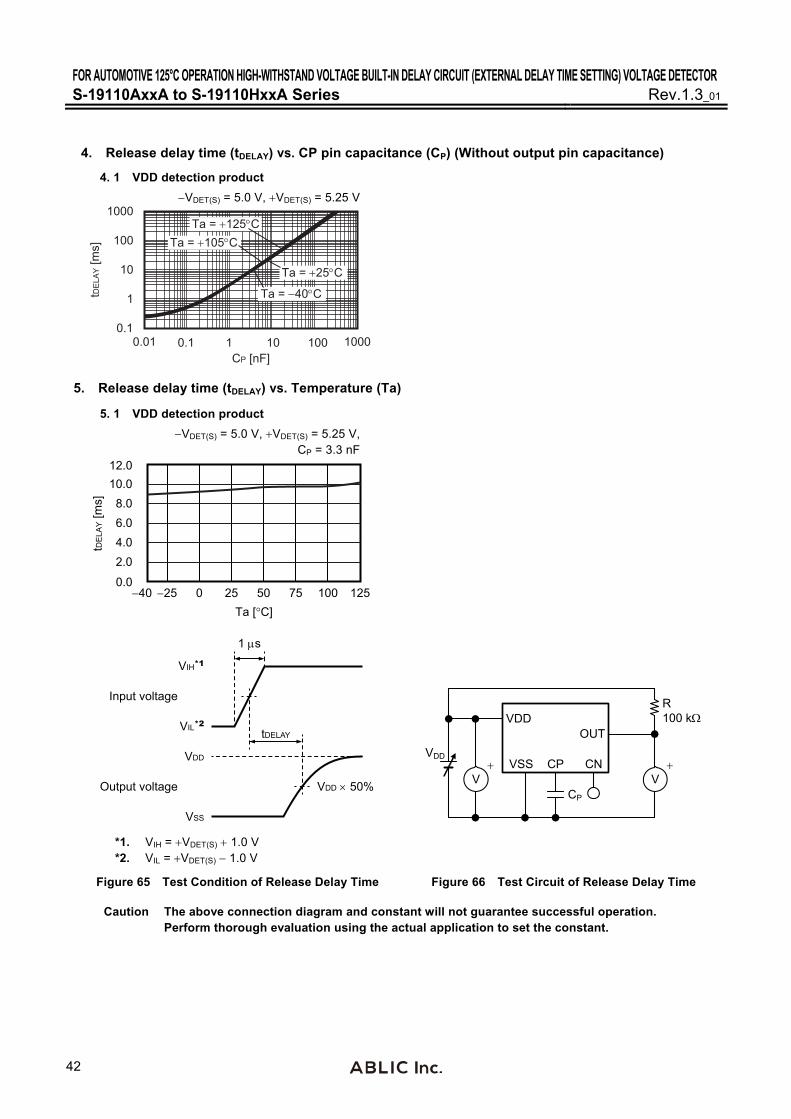
4. Release delay time (tDELAY) vs. CP pin capacitance (CP) (Without output pin capacitance)
4. 1 VDD detection product
VDET(S) = 5.0 V, VDET(S) = 5.25 V
0.01 10000.1
1000
100
1
10
0.1 1 10 100
tDE
LAY [m
s]
CP [nF]
Ta = 40C
Ta = 105C
Ta = 25C
Ta = 125C
5. Release delay time (tDELAY) vs. Temperature (Ta)
5. 1 VDD detection product
VDET(S) = 5.0 V, VDET(S) = 5.25 V, CP = 3.3 nF
Ta [°C]40 25 0 25 50 75 100 125
0.0
12.010.0
8.06.04.02.0
tDE
LAY [m
s]
1 s
tDELAY
VIH*1
Input voltage
Output voltage
VIL*2
VDD
VSS
VDD 50%
VDD
VSS
OUT
CP CN VDD
R 100 k
V
V
CP
*1. VIH = VDET(S) 1.0 V *2. VIL = VDET(S) 1.0 V
Figure 65 Test Condition of Release Delay Time Figure 66 Test Circuit of Release Delay Time
Caution The above connection diagram and constant will not guarantee successful operation. Perform thorough evaluation using the actual application to set the constant.
FOR AUTOMOTIVE 125°C OPERATION HIGH-WITHSTAND VOLTAGE BUILT-IN DELAY CIRCUIT (EXTERNAL DELAY TIME SETTING) VOLTAGE DETECTORRev.1.3_01 S-19110AxxA to S-19110HxxA Series
43
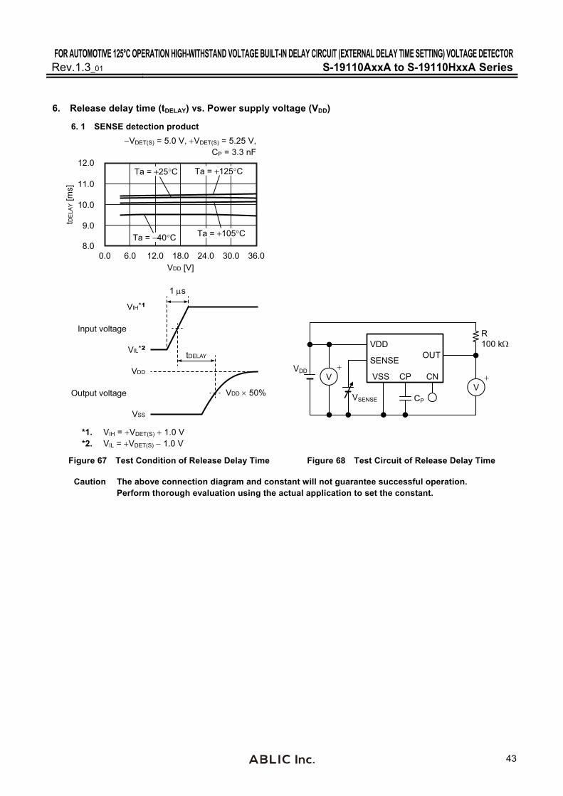
6. Release delay time (tDELAY) vs. Power supply voltage (VDD)
6. 1 SENSE detection product
VDET(S) = 5.0 V, VDET(S) = 5.25 V, CP = 3.3 nF
12.0
8.00.0 36.0
VDD [V]30.024.018.012.06.0
tDE
LAY [m
s] 11.0
10.0
9.0Ta = +105°C
Ta = +25°C
Ta = −40°C
Ta = +125°C
1 s
tDELAY
VIH*1
VIL*2
VDD
VSS
VDD 50%
Input voltage
Output voltage
VDD
VSS
OUT
CP CN
VSENSE
R 100 k
V
CP
VDDV
SENSE
*1. VIH = VDET(S) 1.0 V *2. VIL = VDET(S) 1.0 V
Figure 67 Test Condition of Release Delay Time Figure 68 Test Circuit of Release Delay Time
Caution The above connection diagram and constant will not guarantee successful operation. Perform thorough evaluation using the actual application to set the constant.

FOR AUTOMOTIVE 125°C OPERATION HIGH-WITHSTAND VOLTAGE BUILT-IN DELAY CIRCUIT (EXTERNAL DELAY TIME SETTING) VOLTAGE DETECTOR S-19110AxxA to S-19110HxxA Series Rev.1.3_01
44
Application Circuit Examples
1. Microcomputer reset circuits
In microcomputers, when the power supply voltage is lower than the minimum operation voltage, an unspecified operation may be performed or the contents of the memory register may be lost. When power supply voltage returns to the normal level, the microcomputer needs to be initialized. Otherwise, the microcomputer may malfunction after that. Reset circuits to protect microcomputer in the event of current being momentarily switched off or lowered. Using the S-19110 Series which has the low minimum operation voltage, the high-accuracy detection voltage and the hysteresis width, reset circuits can be easily constructed as seen in Figure 69 and Figure 70.
GND
VDDVDD1
Microcomputer
VDD
VSS OUT
CP CN
GND
VDD1
VDD
VSS
SENSEOUT
CP CN
VSENSEMicrocomputer
Figure 69 Example of Reset Circuit Figure 70 Example of Reset Circuit (VDD Detection Product) (SENSE Detection Product)
Caution The above connection diagram and constant will not guarantee successful operation. Perform thorough evaluation using the actual application to set the constant.
FOR AUTOMOTIVE 125°C OPERATION HIGH-WITHSTAND VOLTAGE BUILT-IN DELAY CIRCUIT (EXTERNAL DELAY TIME SETTING) VOLTAGE DETECTORRev.1.3_01 S-19110AxxA to S-19110HxxA Series
45
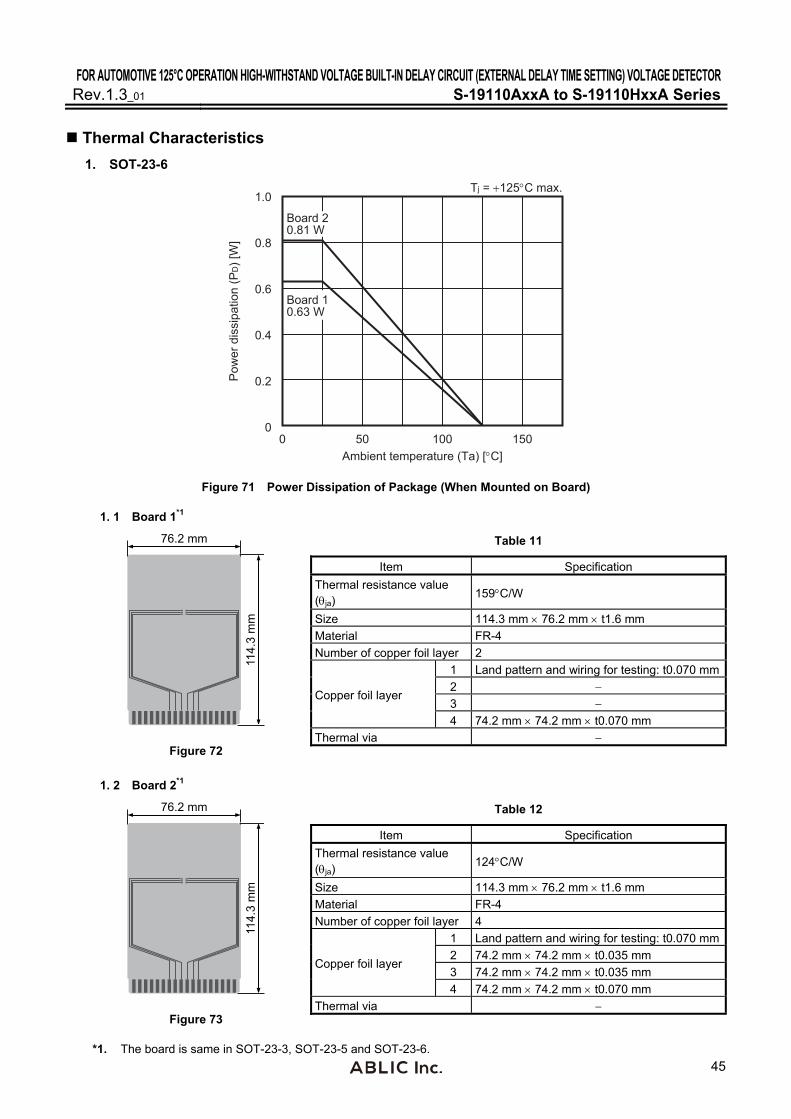
Thermal Characteristics
1. SOT-23-6
0
1.0
0.8
0.6
0.4
0.2
0 10050 150Ambient temperature (Ta) [C]
Pow
er d
issi
patio
n (P
D) [
W]
Tj = 125C max.
Board 20.81 W
Board 10.63 W
Figure 71 Power Dissipation of Package (When Mounted on Board)
1. 1 Board 1*1
76.2 mm
114.
3 m
m
Figure 72
Table 11
Item Specification
Thermal resistance value (ja)
159C/W
Size 114.3 mm 76.2 mm t1.6 mm
Material FR-4
Number of copper foil layer 2
Copper foil layer
1 Land pattern and wiring for testing: t0.070 mm
2 3 4 74.2 mm 74.2 mm t0.070 mm
Thermal via
1. 2 Board 2*1
76.2 mm
114.
3 m
m
Figure 73
Table 12
Item Specification
Thermal resistance value (ja)
124C/W
Size 114.3 mm 76.2 mm t1.6 mm
Material FR-4
Number of copper foil layer 4
Copper foil layer
1 Land pattern and wiring for testing: t0.070 mm
2 74.2 mm 74.2 mm t0.035 mm 3 74.2 mm 74.2 mm t0.035 mm 4 74.2 mm 74.2 mm t0.070 mm
Thermal via
*1. The board is same in SOT-23-3, SOT-23-5 and SOT-23-6.
���
�����
���
����
������ ��
�� ����
����
�� ����
� � �
�� �
���������
�� �
�����������
�� �
��
�������������������
���������������
��������������� !"��!"

���
�����
���
����
������ ��
��
���
� � �
#���������
��������
#��������� �������
�������
��������
�������
�����������$�������
�������$�������
��������$%&& � & � �%'
( )�)�& *+��!
�������,���'�+*- ".��������/
���
�����
���
����
������ ��
��
�����%0�
������
#������
,��1/ ,��1/
2�3 �4���
�!5%&6 )�)&%7�!6��!�+- �* !+&%5�'%&+
�����������8�������
�������8�������
��������8 5

Disclaimers (Handling Precautions)
1. All the information described herein (product data, specifications, figures, tables, programs, algorithms and application circuit examples, etc.) is current as of publishing date of this document and is subject to change without notice.
2. The circuit examples and the usages described herein are for reference only, and do not guarantee the success of any specific mass-production design. ABLIC Inc. is not responsible for damages caused by the reasons other than the products described herein (hereinafter "the products") or infringement of third-party intellectual property right and any other right due to the use of the information described herein.
3. ABLIC Inc. is not responsible for damages caused by the incorrect information described herein.
4. Be careful to use the products within their specified ranges. Pay special attention to the absolute maximum ratings, operation voltage range and electrical characteristics, etc. ABLIC Inc. is not responsible for damages caused by failures and / or accidents, etc. that occur due to the use of the products outside their specified ranges.
5. When using the products, confirm their applications, and the laws and regulations of the region or country where they are used and verify suitability, safety and other factors for the intended use.
6. When exporting the products, comply with the Foreign Exchange and Foreign Trade Act and all other export-related laws, and follow the required procedures.
7. The products must not be used or provided (exported) for the purposes of the development of weapons of mass destruction or military use. ABLIC Inc. is not responsible for any provision (export) to those whose purpose is to develop, manufacture, use or store nuclear, biological or chemical weapons, missiles, or other military use.
8. The products are not designed to be used as part of any device or equipment that may affect the human body, human life, or assets (such as medical equipment, disaster prevention systems, security systems, combustion control systems, infrastructure control systems, vehicle equipment, traffic systems, in-vehicle equipment, aviation equipment, aerospace equipment, and nuclear-related equipment), excluding when specified for in-vehicle use or other uses. Do not apply the products to the above listed devices and equipments without prior written permission by ABLIC Inc. Especially, the products cannot be used for life support devices, devices implanted in the human body and devices that directly affect human life, etc. Prior consultation with our sales office is required when considering the above uses. ABLIC Inc. is not responsible for damages caused by unauthorized or unspecified use of our products.
9. Semiconductor products may fail or malfunction with some probability. The user of the products should therefore take responsibility to give thorough consideration to safety design including redundancy, fire spread prevention measures, and malfunction prevention to prevent accidents causing injury or death, fires and social damage, etc. that may ensue from the products' failure or malfunction. The entire system must be sufficiently evaluated and applied on customer's own responsibility.
10. The products are not designed to be radiation-proof. The necessary radiation measures should be taken in the product design by the customer depending on the intended use.
11. The products do not affect human health under normal use. However, they contain chemical substances and heavy metals and should therefore not be put in the mouth. The fracture surfaces of wafers and chips may be sharp. Be careful when handling these with the bare hands to prevent injuries, etc.
12. When disposing of the products, comply with the laws and ordinances of the country or region where they are used.
13. The information described herein contains copyright information and know-how of ABLIC Inc. The information described herein does not convey any license under any intellectual property rights or any other rights belonging to ABLIC Inc. or a third party. Reproduction or copying of the information from this document or any part of this document described herein for the purpose of disclosing it to a third-party without the express permission of ABLIC Inc. is strictly prohibited.
14. For more details on the information described herein, contact our sales office.
2.0-2018.01
www.ablicinc.com


![Before Use - SMC株式会社 Use Digital Flow Switch PF3A703H/PF3A706H/PF3A712H Change of Set Flow and Hysteresis [Hysteresis mode] (1) Press the S button for 1 second](https://static.fdocument.pub/doc/165x107/5b0997bf7f8b9a520e8e60f5/before-use-smc-use-digital-flow-switch-pf3a703hpf3a706hpf3a712h.jpg)