
Review) ZnO From Basics Towards Applications_PSSB
47
phys. stat. sol. (b) 244, No. 9, 3027– 3073 (2007) / DOI 10.1002/pssb.200743072 © 2007 WILEY-VCH Verlag GmbH & Co. KGaA, Weinheim Review Article Review Article ZnO: From basics towards applications * C. Klingshirn ** Institut für Angewandte Physik der Universität Karlsruhe, Wolfgang-Gaede-Str. 1, 76131 Karlsruhe, Germany Received 14 February 2007, revised 6 June 2007, accepted 6 June 2007 Published online 25 July 2007 PACS 61.72.Vv, 71.35.–y, 78.45.+h, 81.05.Dz, 81.07.–b, 85.60.–q Several hundred thousands of tons of ZnO are used by per year, e.g. as an additive to concrete or to rub- ber. In the field of optoelectronics, ZnO holds promises as a material for a blue/UV optoelectronics, alter- natively to GaN, as a cheap, transparent, conducting oxide, as a material for electronic circuits, which are transparent in the visible or for semiconductor spintronics. The main problem is presently, however, a high, reproducible and stable p-doping. We review in this contribution partly critically the material growth, fundamental properties of ZnO and of ZnO-based nanostructures, doping as well as present and future applications, with emphasis on the electronic and optical properties including stimulated emission. © 2007 WILEY-VCH Verlag GmbH & Co. KGaA, Weinheim 1 Introduction Zinc oxide is a II b – VI compound semiconductor. The II b – VI semiconductors and semimetals comprise the binary compounds of Zn, Cd, and Hg with O, S, Se, and Te and their ternary or quaternary alloys. ZnO is a wide-gap semiconductor with a direct gap around 3.4 eV, i.e. in the near-UV and crystallizes preferentially in the hexagonal wurtzite-type structure. It occurs in nature with the mineral name “zin- cite”. The mineral contains usually a certain amount of Mn and other elements and is of yellow to red color. The ZnO used for the investigations and applications below is exclusively synthetic material. Due to its large bandgap pure ZnO is colorless and clear. The research on ZnO started gradually in the 1930s. This early period is reviewed and documented, e.g. in [1 – 3]. The research peaked around the end of the 1970s and the beginning of the 1980s. Then the interest faded away, partly because it was not possible to dope ZnO both n- and p-type, which is an in- dispensable prerequisite for applications of ZnO in optoelectronics, partly because the interest moved to structures of reduced dimensionality, like quantum wells, which were at that time almost exclusively based on the III – V system GaAs/Al 1–y Ga y As. The emphasis of ZnO research at that time was essentially on bulk samples covering topics like growth, doping, transport, deep centers, band structure, excitons, bulk- and surface-polaritons, luminescence, high excitation or many-particle effects and lasing. The results of this first research period are reviewed, e.g. in [4 – 8] and entered in data collections [9] or in textbooks on semiconductor optics [10]. * This contribution is based on a recent review by the same author [Chem. Phys. Chem. 8, 782 (2007)]. It contains some updates and it goes, in several aspects, into more detail of the semiconductor physics, corresponding to the different readership of the two journals. ** e-mail: [email protected]
-
Upload
batool-fatima -
Category
Documents
-
view
216 -
download
4
Transcript of Review) ZnO From Basics Towards Applications_PSSB

phys. stat. sol. (b) 244, No. 9, 3027–3073 (2007) / DOI 10.1002/pssb.200743072
© 2007 WILEY-VCH Verlag GmbH & Co. KGaA, Weinheim
Review
Article
Review Article
ZnO: From basics towards applications*
C. Klingshirn**
Institut für Angewandte Physik der Universität Karlsruhe, Wolfgang-Gaede-Str. 1, 76131 Karlsruhe,
Germany
Received 14 February 2007, revised 6 June 2007, accepted 6 June 2007
Published online 25 July 2007
PACS 61.72.Vv, 71.35.–y, 78.45.+h, 81.05.Dz, 81.07.–b, 85.60.–q
Several hundred thousands of tons of ZnO are used by per year, e.g. as an additive to concrete or to rub-
ber. In the field of optoelectronics, ZnO holds promises as a material for a blue/UV optoelectronics, alter-
natively to GaN, as a cheap, transparent, conducting oxide, as a material for electronic circuits, which are
transparent in the visible or for semiconductor spintronics. The main problem is presently, however, a
high, reproducible and stable p-doping. We review in this contribution partly critically the material
growth, fundamental properties of ZnO and of ZnO-based nanostructures, doping as well as present and
future applications, with emphasis on the electronic and optical properties including stimulated emission.
© 2007 WILEY-VCH Verlag GmbH & Co. KGaA, Weinheim
1 Introduction
Zinc oxide is a IIb–VI compound semiconductor. The II b–VI semiconductors and semimetals comprise the binary compounds of Zn, Cd, and Hg with O, S, Se, and Te and their ternary or quaternary alloys. ZnO is a wide-gap semiconductor with a direct gap around 3.4 eV, i.e. in the near-UV and crystallizes preferentially in the hexagonal wurtzite-type structure. It occurs in nature with the mineral name “zin-cite”. The mineral contains usually a certain amount of Mn and other elements and is of yellow to red color. The ZnO used for the investigations and applications below is exclusively synthetic material. Due to its large bandgap pure ZnO is colorless and clear. The research on ZnO started gradually in the 1930s. This early period is reviewed and documented, e.g. in [1–3]. The research peaked around the end of the 1970s and the beginning of the 1980s. Then the interest faded away, partly because it was not possible to dope ZnO both n- and p-type, which is an in-dispensable prerequisite for applications of ZnO in optoelectronics, partly because the interest moved to structures of reduced dimensionality, like quantum wells, which were at that time almost exclusively based on the III–V system GaAs/Al1–yGa
yAs. The emphasis of ZnO research at that time was essentially
on bulk samples covering topics like growth, doping, transport, deep centers, band structure, excitons, bulk- and surface-polaritons, luminescence, high excitation or many-particle effects and lasing. The results of this first research period are reviewed, e.g. in [4–8] and entered in data collections [9] or in textbooks on semiconductor optics [10].
* This contribution is based on a recent review by the same author [Chem. Phys. Chem. 8, 782 (2007)]. It contains some updates
and it goes, in several aspects, into more detail of the semiconductor physics, corresponding to the different readership of the
two journals.
** e-mail: [email protected]

3028 C. Klingshirn: ZnO: From basics towards applications
© 2007 WILEY-VCH Verlag GmbH & Co. KGaA, Weinheim www.pss-b.com
The present renaissance on ZnO research started in the mid-1990s and is documented by numerous conferences, workshops, and symposia and by more than 2000 ZnO-related papers in the year 2005 and an even higher number for 2006, compared to slightly beyond 100 in 1970 (sources: INSPEC, Web of Science). The present renaissance is based on the possibility to grow epitaxial layers, quantum wells, nanorods and related objects or quantum dots and on the hope to obtain: – a material for blue/UV optoelectronics, including light emitting or even laser diodes in addition to (or instead of) the GaN-based structures, – a radiation-hard material for electronic devices in a corresponding environment, – a material for electronic circuits that is transparent in the visible and/or usable at elevated tempera-tures, – a diluted- or ferro-magnetic material, when doped with Co, Mn, Fe, V, etc., for semiconductor spin-tronics, – a transparent, highly conducting oxide (TCO), when doped with Al, Ga, In, etc., as a cheaper alter-native to ITO. For several of the above-mentioned applications a stable, high, and reproducible p-doping is obliga-tory. Though progress has been made in this crucial field, as will be outlined below, this aspect still forms a major problem. The emphasis of the present very active period of ZnO research is essentially on the same topics as before, but including nanostructures, new growth and doping techniques and focusing more on applica-tion-related aspects. For first reviews of this new ZnO research period, see, e.g. [11–16]. We shall present or cite in the following deliberately both old and new results covering six decades of ZnO re-search. In the following we will consider first growth and some of the fundamental properties of bulk ZnO and of (nano-) structures of reduced dimensionality with emphasis on (partly critically) reviewing of the electronic and optic properties. The next larger section is devoted to high-excitation effects, stimulated emission and lasing, covering again the range from bulk material over quantum wells and nanorods to quantum dots. In the last section we treat past, present, and visions of possible future applications of ZnO. We give in the following also short introductions to the various concepts of semiconductor optics, which may not be so familiar to the readership. For details we recommend, e.g., Ref. [10].
2 Crystal structure and chemical binding
Zinc oxide crystallizes in the hexagonal wurtzite-type structure shown in Fig. 1. It has a polar hexagonal axis, the c-axis, chosen to be parallel to z. The primitive translation vectors a and b lay in the x–y plane,
Fig. 1 (online colour at: www.pss-b.com) Unit cell of the crystal
structure of ZnO. Light colour – Zn; dark colour – O. (From
Wikipedia.)
phys. stat. sol. (b) 244, No. 9 (2007) 3029
www.pss-b.com © 2007 WILEY-VCH Verlag GmbH & Co. KGaA, Weinheim
Review
Article
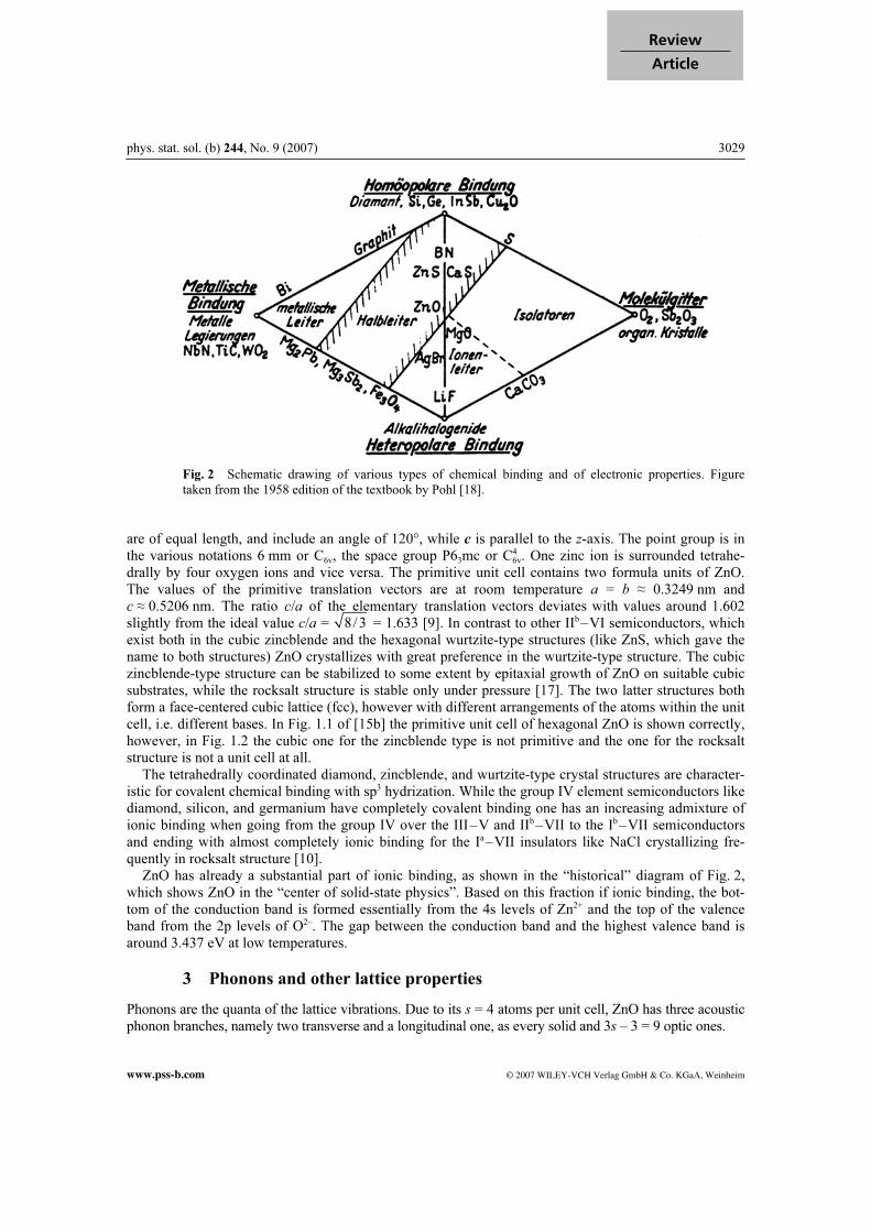
Fig. 2 Schematic drawing of various types of chemical binding and of electronic properties. Figure
taken from the 1958 edition of the textbook by Pohl [18].
are of equal length, and include an angle of 120°, while c is parallel to the z-axis. The point group is in the various notations 6 mm or C6v, the space group P63mc or C4
6v. One zinc ion is surrounded tetrahe-drally by four oxygen ions and vice versa. The primitive unit cell contains two formula units of ZnO. The values of the primitive translation vectors are at room temperature a = b ≈ 0.3249 nm and c ≈ 0.5206 nm. The ratio c/a of the elementary translation vectors deviates with values around 1.602 slightly from the ideal value c/a = 8/3 = 1.633 [9]. In contrast to other IIb–VI semiconductors, which exist both in the cubic zincblende and the hexagonal wurtzite-type structures (like ZnS, which gave the name to both structures) ZnO crystallizes with great preference in the wurtzite-type structure. The cubic zincblende-type structure can be stabilized to some extent by epitaxial growth of ZnO on suitable cubic substrates, while the rocksalt structure is stable only under pressure [17]. The two latter structures both form a face-centered cubic lattice (fcc), however with different arrangements of the atoms within the unit cell, i.e. different bases. In Fig. 1.1 of [15b] the primitive unit cell of hexagonal ZnO is shown correctly, however, in Fig. 1.2 the cubic one for the zincblende type is not primitive and the one for the rocksalt structure is not a unit cell at all. The tetrahedrally coordinated diamond, zincblende, and wurtzite-type crystal structures are character-istic for covalent chemical binding with sp3 hydrization. While the group IV element semiconductors like diamond, silicon, and germanium have completely covalent binding one has an increasing admixture of ionic binding when going from the group IV over the III–V and IIb–VII to the Ib–VII semiconductors and ending with almost completely ionic binding for the Ia–VII insulators like NaCl crystallizing fre-quently in rocksalt structure [10]. ZnO has already a substantial part of ionic binding, as shown in the “historical” diagram of Fig. 2, which shows ZnO in the “center of solid-state physics”. Based on this fraction if ionic binding, the bot-tom of the conduction band is formed essentially from the 4s levels of Zn2+ and the top of the valence band from the 2p levels of O2–. The gap between the conduction band and the highest valence band is around 3.437 eV at low temperatures.
3 Phonons and other lattice properties
Phonons are the quanta of the lattice vibrations. Due to its s = 4 atoms per unit cell, ZnO has three acoustic phonon branches, namely two transverse and a longitudinal one, as every solid and 3s – 3 = 9 optic ones.

3030 C. Klingshirn: ZnO: From basics towards applications
© 2007 WILEY-VCH Verlag GmbH & Co. KGaA, Weinheim www.pss-b.com
Table 1 Symmetries and eigenenergies of the optical phonons of ZnO at the Г-point. The typical accu-
racy or spread of the energies is ±5 cm–1 or ±1 meV. From [4, 9].
irreducible representation eigenenergy degeneracy
E2 low Г6 100 cm–1 12.3 meV 2 B1 low Г3 240 cm1 29.7 meV 1 E2 high Г6 440 cm1 54.5 meV 2 B1 high Г3 540 cm–1 66.9 meV 1 A1 Г1 TO 380 cm–1
LO 577 cm–1
47.1 meV 71.5 meV
1
E1 Г5 TO 410 cm1 LO 590 cm–1
50.8 meV 72.5 meV
2
The eigenenergies of the optical phonons at k = 0, i.e. at the Г-point, the center of the first Brillouin zone, range according to [9] from 12.3 to 72.5 meV. The Г1 and Г5 states are optically dipole allowed for the polarizations E || c and E^ c, respectively, where c is the polar hexagonal axis, and result in the IR in distinct stop- (or Reststrahl-) bands with transverse and longitudinal eigenfrequencies around 50 and 72 meV. The Г1, Г5, Г6 modes are also observed in Raman scattering [9, 15, 20]. The fact that some pho-non modes are seen both in the IR spectra as stop-bands and in Raman spectra is due to the fact that the wurtzite structure does not have a center of inversion, i.e. the parity of the wavefunctions is not a good quantum number [10, 19, 20]. For recent data on isotopically pure ZnO, where phonons no longer show inhomogeneous broadening due to the different isotope masses, see [20a]. Amongst others it has been found from impulsive Raman scattering that the lifetime (more precisely dephasing time) of the E2 low mode can be a few hundred ps at low temperatures or that the Zn mass affects the acoustic phonons and thus the low-temperature spe-cific heat, while the O mass influences mainly the optical phonons. Another recent topic is the investigation of the influence of relatively high doping or even amalgama-tion of ZnO with, e.g. Co, Mn and others on the Raman spectra. This technique allows, e.g. identification of clusters that are not seen in XRD or surface effects [20b]. Other topics are the investigation of the dielectric function [20c] or the phonons in nanocrystals [20d]. The facts that ZnO has (partial) ionic binding and lacks a center of inversion are also the origin of the piezoelectricity of ZnO. The three coefficients of the piezoelectric tensor d15, d31, and d33 are with values around –10, –5, and 12 × 10–12 m/V, respectively, rather large [9, 13, 21]. For the elastic coefficients of ZnO, its hardness, and its thermal properties like specific heat, Debye temperature or thermal conductivity, see [9], and references therein.
4 Growth
Bulk ZnO samples are grown by various techniques. A possibility to grow ZnO by gas transport is given by the following reactions
ZnO + H2 → Zn + H2O , 2Zn + O2 → 2ZnO . (1)
Sometimes graphite is used for the reduction of Zn instead of H2. Pressed or sintered samples of high-purity ZnO powder are reduced to Zn vapor at elevated tempera-tures by hydrogen (or the addition of graphite) which is transported with a flow of inert gas like N2. The zinc vapor is then oxidized in a region of lower temperature under the admission of oxygen or air. Plate-lets and particularly beautiful hexagonal needles can be grown with diameters up to several mm and length of several cm. See, e.g. Fig. 3a. Sometimes crystals develop during this process not a pointed top but umbrella-like shapes with a plane ^c. See, e.g. [16]. Alternatively, one can start directly with Zn vapor. Some selected references for gas-transport techniques are, e.g. [22, 23].

phys. stat. sol. (b) 244, No. 9 (2007) 3031
www.pss-b.com © 2007 WILEY-VCH Verlag GmbH & Co. KGaA, Weinheim
Review
Article
a b
Fig. 3 ZnO single crystals grown by gas transport (a) and by hydrothermal growth (b). From [23] and
[25], respectively.
Another technique that results in samples of many cm3 of volume (Fig. 3b) and that allows production of wavers of several cm2 for homo- or hetero-epitaxy is the hydrothermal growth technique [24, 25]. In this case, ZnO is dissolved at high temperatures and pressure in a KOH/LiOH base in an autoclave and precipitated at regions of reduced temperature. Other techniques include growth from melt or flux [26]. These techniques also allow the growth of large samples. For the production of textured or epitaxial layers and thin films, including quantum wells, there are also a variety of methods available. For early examples of ZnO epitaxy, see [27–29]. A relatively simple technique is to evaporate a thin and homogeneous layer of Zn, e.g. on a plate of quartz glass and to oxi-dize it afterwards at elevated temperatures [28]. This procedure results in at least textured ZnO layers with the c-axis normal to the substrate. The optical properties of such layers tend to be almost identical over more than 6 decades [28, 30]. Another simple possibility is close-spaced evaporation of ZnO on sapphire (Al2O3) substrates with various orientations [29]. The substrates suitable for epitaxy of ZnO are, e.g. Al2O3 partly with a GaN buffer, the latter also having wurtzite structure and only a small lattice mismatch to ZnO of 1.8%. There has been a large range of other substrates that have been used for epitaxial ZnO growth, like Zn [27], SiO2, AlN, SiC, Si, GaAs, or more exotic ones like ScAlMgO4, LiTaO3, LiNbO3 [19] and of course ZnO for homoepitaxy. Surpris-ingly homoepitaxy of ZnO is not a trivial task. From the large number of relevant papers we can give only a tiny selection in [31]. See also [12–15]. The presently mainly used epitaxial methods to grow epilayers or even quantum wells (either ZnO wells with Mg1–yZn
yO barriers or Zn1–yCd
yO wells between ZnO barriers) are partly the standard ones like
molecular beam epitaxy (MBE), metal-organic chemical vapor deposition/metal-organic vapor phase epitaxy (MOCVP/MOVPE) using the decomposition and subsequent ZnO formation of zinc compounds like dimethyl or diethyl-zinc with an oxygen source like O2, H2O2, N2O, NO2, isopropanol, tertiary butonal or acetone on a heated substrate. It should be noted that MgO and CdO crystallize in the NaCl structure. Consequently the incorporation of larger mole fractions of Mg and especially of Cd in Zn1–yMg
yO or Zn1–yCd
yO reduces the sample quality [31, 32]. Due to the piezoelectric effect, superlattices
and quantum wells may have strong internal electric fields if grown on polar surfaces. A technique that is widely used for the production of high-Tc superconductors, is now also frequently used to produce ZnO films namely pulsed laser deposition (PLD) [13, 14, 21, 32]. In this technique, pulsed ns or ps lasers generally emitting in the near-UV like excimer or frequency-tripled Nd YAG lasers are focused tightly on a pressed or sintered ZnO target producing a plume of evaporating source material that is deposited on a heated substrate. The plume is emitted normal to the target surface, independent of the angle of incidence of the incident laser beam and the angle of aperture of the plume narrows with increasing laser pulse energy. The high kinetic energy of the evaporating species results in a high surface

3032 C. Klingshirn: ZnO: From basics towards applications
© 2007 WILEY-VCH Verlag GmbH & Co. KGaA, Weinheim www.pss-b.com
a b
dc
e f
Fig. 4 A few examples of ZnO nanorods and tetrapods. From Sauer and Thonke (a), Waag (b), Grund-
mann (c) [35], and Wissinger (d) [36], partly grown by the VLS process and showing the Au droplet on
top as in (a), a puff-ball of ZnO nanorods occurring occasionally during the growth (e) [23], and an early
example of ZnO tetrapods, by Fuller [38], shown with a magnification of 3500 (f).
mobility on the substrate. A low background pressure of O2 in the otherwise evacuated growth recipient of the PLD process or a post-growth annealing in O2 atmosphere helps to improve the stoichiometry of the ZnO layers. The layers grown by the various techniques mentioned above are not necessarily smooth and perfect epilayers. Often one obtains grains or columnar structures with small hexagonal pyramides on the sur-
phys. stat. sol. (b) 244, No. 9 (2007) 3033
www.pss-b.com © 2007 WILEY-VCH Verlag GmbH & Co. KGaA, Weinheim
Review
Article
face with surface roughness from a few to a few tens of nm. Furthermore, layers and bulk samples may contain strain. Consequently, the FWHM of X-ray rocking curves, of Ω or of θ–2θ scans are often in the range from tens of arc sec to fractions of a degree. A (0002) Ω-scan of a high-quality single crystal grown by [23] shows an almost resolution-limited width of 0.0025° = 8.7″ [16, 33]. Methods to produce large-area polycrystalline layers are, e.g. rf- or magneton-sputtering, e.g. for the production of ZnO:Al as transparent conducting oxide layers, spray pyrolysis, sol–gel techniques or electrochemical deposition [34]. ZnO has a strong tendency for self-organized growth. As a consequence, a very hot topic is presently the growth of whisker-like ZnO nanorods [32, 35]. These are needle-like crystals with diameters in the range of a few tens to a few hundred nm and lengths of several µm. In Fig. 4a–d we give a few recent examples and in Fig. 4e an older one. The methods to grow such nanorods include the above-mentioned ones like PLD, MBE, or MOCVD. A special growth procedure is the so-called vapor–liquid–solid (VLS) process. In this process small metal clusters (usually gold) of a few tens of nm in diameter are deposited on a substrate. The substrate with the Au dots is heated so that the Au melts and forms a drop-let. If Zn vapor is offered, Zn forms an alloy with the Au lowering the melting point. If this alloy is su-persaturated, ZnO nanorods start to grow in the presence of oxygen at the position of the Au droplets. The Au droplets act as catalyst and sit on top of the growing nanorods and growth continues as long as zinc and oxygen are available and the temperature of the alloy stays above the eutectic temperature of the alloy (Fig. 4a). The diameter of the growing nanorods is given by the diameter of the Au droplet. The orientation of the needles in the x–y plane is given by the substrate with c perpendicular to it. Some-times, some of the Au remains at the interface to the substrate [101]. In the meantime, scientists were successful in growing nanorods without the Au droplet catalyst in a self-activated process and in growing them on noncrystalline substrates like glass or plastic sheets. Recently, it has even become possible to grow single quantum wells or superlattices (ZnO/Zn1–yMg
yO) into such nanorods [35]. Apart from the
“simple” nanorods of Fig. 4, ZnO likes to grow under suitable conditions also as nanotetrapods, -combs, -brushes, -nails, -tubes, -walls, -flowers, -corals, -castles, or -propellers [35–38]. Some of the ZnO layers of these various nanostructures would have been considered one or two decades ago as unsuccessful attempts to produce a good epitaxial layer and ended up in the wastebin. It should be acknowledged that the growth of ZnO tetrapods or whiskers is not new, but goes back partly more than six decades as shown in Fig. 4e and f. To reduce the quasidimensionality of ZnO nanostructures even further, one tried successfully to grow quasi-zero-dimensional ZnO quantum dots (QD), also known as nanocrystals, quantum boxes, nanois-lands, or artificial atoms [10]. These are crystallites with typical dimensions of a few nm in all three directions of space, surrounded by a material with a higher bandgap or air.
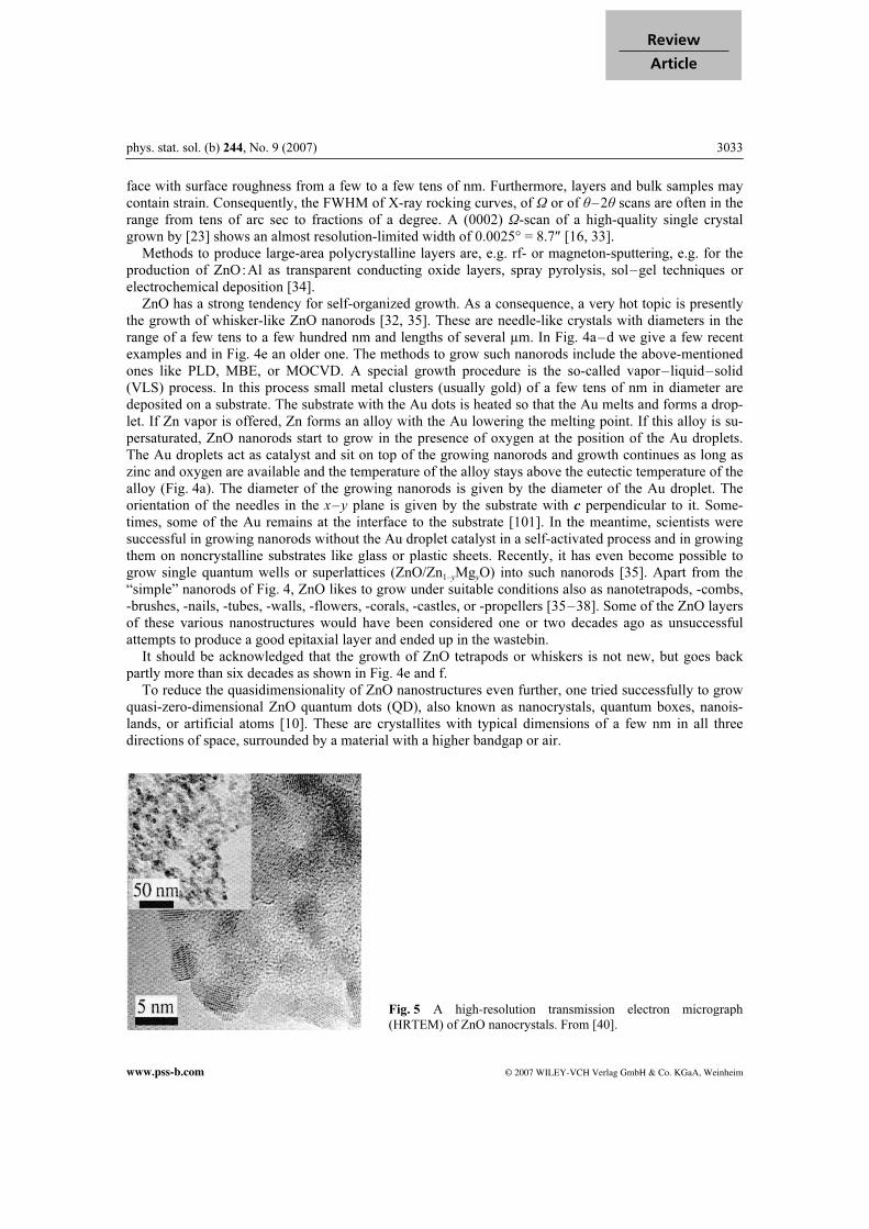
Fig. 5 A high-resolution transmission electron micrograph
(HRTEM) of ZnO nanocrystals. From [40].

3034 C. Klingshirn: ZnO: From basics towards applications
© 2007 WILEY-VCH Verlag GmbH & Co. KGaA, Weinheim www.pss-b.com
The techniques for the production of such ZnO QD are again manifold and include spray pyrolysis, the precipitation of ZnO from aqueous solutions, from sol–gel systems or in glass matrices during an annealing process or in voids of crystals like zeolites or self-assembling in a Stranski–Krastanov or Volmer–Weber epitaxial growth mode or by hydrolysing Zn(CH300)2 in methanol [39]. In Fig. 5 we give as an example a high-resolution transmission electron microscope (HRTEM) image of ZnO QD grown by spray combustion of Zn/Si precursors resulting in ZnO QD in an (amorphous) silica matrix. The lattice planes of the crystallites are clearly visible.
5 Electronic band structure
The band structure gives the electronic one-particle (i.e. electron or hole) states. Since ZnO is a direct gap semiconductor with the global extrema of the upmost valence and the lowest conduction bands (VB and CB, respectively) at the same point in the Brillouin zone, namely at k = 0, i.e. at the Г-point, we are mainly interested in this region. The lowest CB is formed, as already mentioned, from the empty 4s states of Zn2+ or the antibinding sp3 hybrid states. The group-theoretical compatibility tables (see, e.g. [10] and references therein) tell us that the bottom of the CB has Г1 symmetry without inclusion of spin and symmetry Г1 ƒ Г7 = Г7 with spin (Fig. 6). The effective electron (more precisely polaron) mass is almost isotropic with a value around me = (0.28 ± 0.02)m0 [9]. The VB, originating from the occupied 2p orbitals of O2– or the binding sp3 orbitals, are split without spin under the influence of the hexagonal crystal field into two states, Г5 and Г1. Inclusion of spin gives a further splitting due to spin-orbit coupling into three two-fold-degenerate sub-VB of symmetries (Г1 ≈ Г5) ƒ Г7 = Г7 ≈ Г9 ≈ Г7, see Fig. 6. These VB are labelled in all wurtzite-type semiconductors (like ZnS, CdS, CdSe, or GaN) from higher to lower energies as A, B, and C bands. In most cases the ordering of the bands is A Г9, B Г7, C Г7 and the spin–orbit splitting is larger than the crystal field split-ting. In ZnO there is, however, a long-standing debate over whether the ordering of the VB is the usual one [41] or if it is A Г7, B Г9, C Г7 called “negative spin–orbit coupling” or inverted VB ordering [42]. Actually, the spin–orbit coupling is always positive. But due to the small nuclear charge of oxygen it is expected from an extrapolation of the data of the hexagonal and cubic IIb sulfides, selenides, and tellu-rides to the oxides be only around 15 meV, see Fig. 7. The level repulsion with the close-lying occupied
k
ECB
VB
AB
C
Zn 4s++
O 2p– –
Γ7
Γ7
Γ7
Γ9
cE ||
cE⊥
Fig. 6 (online colour at: www.pss-b.com) Valence and
conduction bands of ZnO in the vicinity of the fundamental
bandgap.
phys. stat. sol. (b) 244, No. 9 (2007) 3035
www.pss-b.com © 2007 WILEY-VCH Verlag GmbH & Co. KGaA, Weinheim
Review
Article
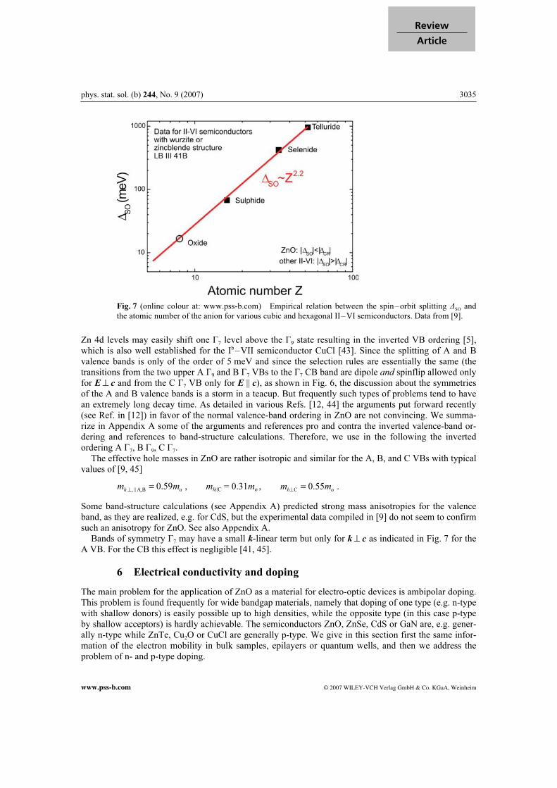
Fig. 7 (online colour at: www.pss-b.com) Empirical relation between the spin–orbit splitting ∆SO
and
the atomic number of the anion for various cubic and hexagonal II–VI semiconductors. Data from [9].
Zn 4d levels may easily shift one Г7 level above the Г9 state resulting in the inverted VB ordering [5], which is also well established for the Ib–VII semiconductor CuCl [43]. Since the splitting of A and B valence bands is only of the order of 5 meV and since the selection rules are essentially the same (the transitions from the two upper A Г9 and B Г7 VBs to the Г7 CB band are dipole and spinflip allowed only for E^ c and from the C Г7 VB only for E || c), as shown in Fig. 6, the discussion about the symmetries of the A and B valence bands is a storm in a teacup. But frequently such types of problems tend to have an extremely long decay time. As detailed in various Refs. [12, 44] the arguments put forward recently (see Ref. in [12]) in favor of the normal valence-band ordering in ZnO are not convincing. We summa-rize in Appendix A some of the arguments and references pro and contra the inverted valence-band or-dering and references to band-structure calculations. Therefore, we use in the following the inverted ordering A Г7, B Г9, C Г7. The effective hole masses in ZnO are rather isotropic and similar for the A, B, and C VBs with typical values of [9, 45]
, || A,B o0.59h
m m^
= , mh||C = 0.31mo , C o
0.55h
m m^
= .
Some band-structure calculations (see Appendix A) predicted strong mass anisotropies for the valence band, as they are realized, e.g. for CdS, but the experimental data compiled in [9] do not seem to confirm such an anisotropy for ZnO. See also Appendix A. Bands of symmetry Г7 may have a small k-linear term but only for k^ c as indicated in Fig. 7 for the A VB. For the CB this effect is negligible [41, 45].
6 Electrical conductivity and doping
The main problem for the application of ZnO as a material for electro-optic devices is ambipolar doping. This problem is found frequently for wide bandgap materials, namely that doping of one type (e.g. n-type with shallow donors) is easily possible up to high densities, while the opposite type (in this case p-type by shallow acceptors) is hardly achievable. The semiconductors ZnO, ZnSe, CdS or GaN are, e.g. gener-ally n-type while ZnTe, Cu2O or CuCl are generally p-type. We give in this section first the same infor-mation of the electron mobility in bulk samples, epilayers or quantum wells, and then we address the problem of n- and p-type doping.
3036 C. Klingshirn: ZnO: From basics towards applications
© 2007 WILEY-VCH Verlag GmbH & Co. KGaA, Weinheim www.pss-b.com
6.1 Hall mobility
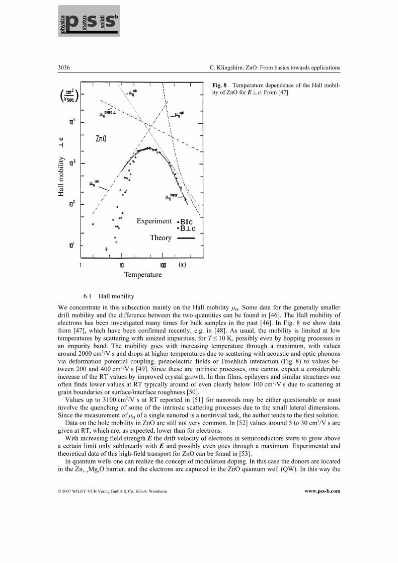
We concentrate in this subsection mainly on the Hall mobility µH. Some data for the generally smaller drift mobility and the difference between the two quantities can be found in [46]. The Hall mobility of electrons has been investigated many times for bulk samples in the past [46]. In Fig. 8 we show data from [47], which have been confirmed recently, e.g. in [48]. As usual, the mobility is limited at low temperatures by scattering with ionized impurities, for T ≤ 10 K, possibly even by hopping processes in an impurity band. The mobility goes with increasing temperature through a maximum, with values around 2000 cm2/V s and drops at higher temperatures due to scattering with acoustic and optic phonons via deformation potential coupling, piezoelectric fields or Froehlich interaction (Fig. 8) to values be-tween 200 and 400 cm2/V s [49]. Since these are intrinsic processes, one cannot expect a considerable increase of the RT values by improved crystal growth. In thin films, epilayers and similar structures one often finds lower values at RT typically around or even clearly below 100 cm2/V s due to scattering at grain boundaries or surface/interface roughness [50]. Values up to 3100 cm2/V s at RT reported in [51] for nanorods may be either questionable or must involve the quenching of some of the intrinsic scattering processes due to the small lateral dimensions. Since the measurement of µH of a single nanorod is a nontrivial task, the author tends to the first solution. Data on the hole mobility in ZnO are still not very common. In [52] values around 5 to 30 cm2/V s are given at RT, which are, as expected, lower than for electrons. With increasing field strength E the drift velocity of electrons in semiconductors starts to grow above a certain limit only sublinearly with E and possibly even goes through a maximum. Experimental and theoretical data of this high-field transport for ZnO can be found in [53]. In quantum wells one can realize the concept of modulation doping. In this case the donors are located in the Zn1–yMgyO barrier, and the electrons are captured in the ZnO quantum well (QW). In this way the
Fig. 8 Temperature dependence of the Hall mobil-
ity of ZnO for E ^ c. From [47].

phys. stat. sol. (b) 244, No. 9 (2007) 3037
www.pss-b.com © 2007 WILEY-VCH Verlag GmbH & Co. KGaA, Weinheim
Review
Article
free carriers can be separated spatially from the ionized donors, reducing thus the scattering rate with these defects. As a result, low-temperature mobilities up to 2700 cm2/V s have been reported in ZnO QW [54, 55]. Such values allow observation of the (integer) quantum Hall effect in ZnO. For the first reports see [55].
6.2 n-type doping
For n-type doping one would chose to substitute Zn or O with atoms that have one electron more in the outer shell than the atom which they replace. Consequently the group III elements Al, Ga, and In are shallow and efficient donors on Zn cation sites according to
D0 ¤ D+ + e , (2)
where D0 and D+ are the neutral and ionized donors, respectively, and the equilibrium is at RT essentially on the r.h.s. of Eq. (2). Indeed, electron concentrations beyond 1020 cm–3 are obtained in ZnO:Al or ZnO:Ga, which result even at room temperature in a degenerate electron gas in the conduction band. For a few references including also the UV and IR optical properties see, e.g. [56, 57]. A degenerate carrier gas is characterized by the fact that the Fermi energy is located in the band and no longer in the bandgap and that consequently Fermi–Dirac statistics is mandatory for an adequate description. The limit be-tween a description in terms of classical Boltzmann and degenerate Fermi–Dirac statistics is the so-called effective density of states, which is for ZnO at RT given by [10]
3/ 2
18 3e B
eff 2
2π2 4 10 cm
m k Tn
h
-Ê ˆ= = ¥Ë ¯ . (3)
At densities around 1020 cm–3 the screened plasma frequency ω0Pl given for k = 0 by
1/ 22
0
Pl
0 b 0
ne
m
ω
ε ε
Ê ˆ= Á ˜Ë ¯, (4)
where ε0 = 8.85 × 10⁻¹² As/Vm and εb is the background dielectric constant for Pl,ω ω
0 corresponds to
photon energies ћω0Pl of a few hundred meV. Consequently such highly doped samples show high reflec-
tivity from ω = 0 to the longitudinal energy ћω0Pl situated in the near-IR with some peculiarities around
optically active phonon modes (see above) due to the formation of plasmon phonon mixed state quanta [57a]. The THz conductivity and dielectric properties of ZnO and ZnO nanostructures have been investi-gated in [57b]. The other possibility for n-doping would be group VII elements on the anion site. Though this combi-nation is known to be very efficient, e.g. for ZnSe:Cl [58] it has been less investigated for ZnO. Fur-thermore, it has been shown that hydrogen is always a donor in ZnO [59]. This might be, together with small deviations from stoichiometry, a reason why ZnO without intentional doping is always n-type.
6.3 p-type doping
According to the above rules, one would expect that the group I elements Li, Na, or K are good acceptors on Zn site. Indeed Li, Na, K, and also the Ib elements Cu and Ag are known to form acceptors. However, they usually form deep acceptors with ionization energies around a few hundred meV [60, 61], i.e. much larger than kBT at room temperature. As a consequence, the equilibrium is at RT on the l.h.s. of Eq. (5):
A0 ¤ A h-
+ . (5)
Therefore, e.g. ZnO:Li is a high-resistivity material but does not show good p-type conductivity at RT. Some ZnO samples have been doped so strongly with Li that they showed cracks and precipitations, but still remained high-resistivity material [60]. In addition, interstitial Li (or Ag) occurring at high doping levels may act as a donor, as has been known for more than four decades, thus compensating part of the
3038 C. Klingshirn: ZnO: From basics towards applications
© 2007 WILEY-VCH Verlag GmbH & Co. KGaA, Weinheim www.pss-b.com
acceptors [60]. Samples grown by the hydrothermal technique from LiOH/KOH bases necessarily have a high incorporation of these cations, are consequently high-resistively materials and it is difficult to obtain for them good n-type doping due to compensation of acceptors and donors. As a consequence of these problems, a lot of research presently concentrates on p-type doping with the group V elements N, P, As and even Sb on O sites. After a lot of poorly reproducible results and other problems summarized beautifully by, e.g. Look et al. [61], there were recently reliable reports on p-type doping in ZnO with N, As or P, see, e.g. [61]. The nitrogen acceptor has, with about 100 meV, possibly even a smaller ionization energy than the standard acceptor Mg in GaN:Mg with 160 meV. The doping level is, with values generally well below or around 1018 cm–3, still limited and partly also the solubility of the group V elements on O sites. One hopes to make some progress by codoping, i.e. by using either two different acceptors simultaneously like ZnO:N,As or ZnO:Li,N or by combining even a moderate concentration of donors with a higher concentration of acceptors, e.g. in ZnO:Ga,N [61]. Fur-thermore, it has been claimed that Li may form a complex in ZnO with a relatively low ionization energy of 130 meV [62], which in turn provides an argument to assign the deepest bound-exciton complexes like I10 again to acceptor bound-exciton complexes (see Section 9.2). Not all incorporated doping atoms form the desired shallow acceptors, with the consequence that the hole concentration is usually much smaller than the concentration of dopant atoms. This statement is illustrated by the strong deep center luminescence of p-type ZnO. An example will be given later with Fig. 26.
7 Deep centers
While efficient donors or acceptors have energy levels close to the conduction or valence band, respec-tively, there are also deep centers with levels energetically deep in the forbidden gap. We have men-tioned already deep acceptor levels situated energetically a few hundred meV above the valence band. The light emission resulting from the recombination of a free electron in the conduction band with a hole bound, e.g. to a Li acceptor, is situated therefore in the yellow spectral range (see the work by Zwingel in [60]), while the intrinsic luminescence processes result in blue or near-UV emission as we shall see in Section 9. There are many other deep centers known in ZnO, like Cu, Fe, Co, Mn, OH, etc. as extrinsic ones and intrinsic ones like oxygen vacancies or zinc interstitials. Concerning the optical properties, deep centers may lead to additional absorption bands. ZnO:Cu or ZnO:Co show, e.g. different green colors. Concerning the light emission, deep centers may lead to emission bands at photon energies significantly below the gap either due to free to bound transitions like the yellow emission of ZnO:Li mentioned
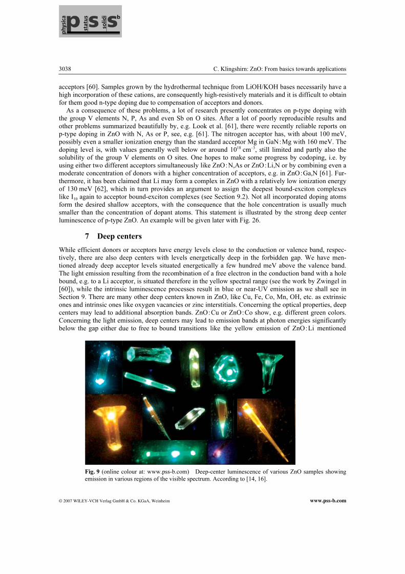
Fig. 9 (online colour at: www.pss-b.com) Deep-center luminescence of various ZnO samples showing
emission in various regions of the visible spectrum. According to [14, 16].

phys. stat. sol. (b) 244, No. 9 (2007) 3039
www.pss-b.com © 2007 WILEY-VCH Verlag GmbH & Co. KGaA, Weinheim
Review
Article
above or due to internal transition within the center like the green emission in ZnO:Cu showing a broad emission band with a clear phononic structure [10]. In Fig. 9 we show an overview of various emission bands. Red emission results from ZnO:Fe, green emission can come, apart from Cu centers, also from oxygen vacancies showing a smooth spectrum. However, recently, further centers have been put forward to explain the green luminescence like ZnO:V instead of ZnO:Cu or an oxide antisite OZn instead of vacancies (VO, VZn) or Zni. Recently, other intrinsic defects like vacancies and interstitials of Zn and O have been also discussed as the origin of emission bands from the yellow-orange to the purple spectral range. Such deep center luminescence allows light emission to be obtained from ZnO not only close to the intrinsic absorption edge, which is in the near-UV, but also over the whole visible spectrum. For a few of the many papers on deep centers in ZnO see [9, 60, 63–65]. In ZnO powders an external luminescence yield at low temperatures up to several tens of per cent has been determined for a green luminescence band [66]. It should be mentioned that, however, some deep centers may act also as luminescence killers at higher concentrations like Cu or Fe.
8 Magnetic properties
A topic that results in a wealth of beautiful physical phenomena, are so-called diluted- or semimagnetic semiconductors (DMS). These are semiconductors that are doped or alloyed with a substantial fraction (from 1% up to around 10%) of magnetic ions like Mn, Fe, Co, V, etc. Due to the coupling of the spins of free carriers with the spins of the magnetic ions surprising effects can be observed like a giant Zeeman splitting with effective g values around 100, e.g. in Zn1–xMn
xSe or the formation of magnetic polarons.
These are free electrons that carry with them a cloud of aligned spins of the surrounding magnetic ions. Some of the DMS exhibit ferromagnetism up to RT like ZnO:Co or ZnO:Mn or GaAs:Mn from the III–V semiconductors. In Fig. 10 we show as an example the hysteresis loop of a Zn1–xMn
xO film at low
and room temperature. Presently, there is a vivid and controversial discussion going on as to what extent this ferromagnetism is due to the doped ZnO:X (X = Mn, Co, V, . . .) matrix itself or due to clusters or precipitates of other phases [67, 68]. The absence of additional peaks in XRD turned out not to be suffi-cient to rule out secondary phases, see, e.g. the work by Zhou in [20b]. Some theoretical models predict RT ferromagnetism in DMS ZnO only for completely unrealistic high p-doping levels. See, e.g. the work by Dietl in [68]. The magnetization is frequently given in the rather strange “electromagnetic units” (emu) or in emu/g. Typical values are in the range of 10–2 to 10–5 emu. The following relation holds between the various
Fig. 10 Ferromagnetic hysteresis loops of Mn containing ZnO for two different temperatures. From [67].

3040 C. Klingshirn: ZnO: From basics towards applications
© 2007 WILEY-VCH Verlag GmbH & Co. KGaA, Weinheim www.pss-b.com
units of the magnetic field according to B = µ0(H + M)
1 emu = 10–3 A/m , 1 A/m = 4π 10–7 V s/A m = 4π 10–7 T . (6)
Consequently, the magnetic field connected with a ferromagnetic DMS is orders of magnitude below the magnetic field of the Earth, which is a few tens of µT. Though DMS allow beautiful physics to be per-formed in experiment and theory, these numbers (and not only these numbers) cast some serious doubts on the highly speculative concept of semiconductor spintronics and even more on the field of quantum computing using spintronics. The author feels that this aspect is not only relevant for the II–VI DMS [10].
9 Linear optical properties
We have mentioned the optical properties connected with optical phonons, with plasmons in highly doped samples and the resulting plasmon–phonon mixed states, already in Sections 3 and 6 and the properties of deep centers in Section 7. Here, and in the following sections, we concentrate on the elec-tronic optical properties close to the fundamental absorption edge, which is, as already mentioned in the introduction, in ZnO in the blue/near-UV range.
9.1 Free excitons and exciton-polaritons
The simplest way to describe the expected absorption spectrum in a direct-gap semiconductor with a dipole allowed band-to-band transition like ZnO is in terms of this band-to-band transition as shown in Fig. 6. A photon with an energy larger than the bandgap excites an electron from the VB to the CB. Since the density of states varies in three dimensions for a parabolic E(k) relation as the square-root of the energy, one would expect on this level, the onset of the absorption spectrum α(ћω) according to
gg
for( )
otherwise0
EE ωω
α ω
≥Ï -µÌÓ
. (7)
Indeed, this picture is too simple to be compatible with reality. We see already from Fig. 6 that an ab-sorption process is a two-particle transition, i.e. by the absorption of a photon simultaneously an electron in the CB and a hole in the VB are created. Similarly, two particles are annihilated in a radiative or non-radiative recombination process. The point is now that the electron and hole interact via their attractive Coulomb potential, forming a series of hydrogen- or positronium-like states below the gap, Fig. 11a. These states are called excitons. The excitons are the quanta of the excitation in the electronic system of semiconductors or insulators. The ground state is a semiconductor with completely filled VB and empty CB. It has energy E = 0 and total momentum ћk = 0. The series of hydrogen-like exciton states with main quantum number nB = 1, 2, 3 . . . is followed by the ionization continuum, starting at Eg. The excitonic binding or Rydberg energy (E
x
b or Ry*) is in ZnO for all three exciton series resulting from the transitions from the A, B, and C
VB (Fig. 6) into the conduction band roughly equal Ex
b ≈ 60 meV [5, 6, 45]. In [69] lower values of 53 and 49 meV have been given for the B and C excitons. These numbers result from the unusual proce-dure to count the binding energy from the reflection minimum (Fig. 12), which coincides closely with the longitudinal energy (see below). Usually, one counts from either the transverse exciton energy to the bandgap or the slightly (≤1 meV) lower-lying spin-triplet [70] state. If the value of the longitudinal–transverse splitting ∆LT is added to the numbers from [69] above, one ends up with the usual and long-known value of the binding energy around 60 meV for A, B, and C exciton states. The deviations from the data of hydrogen (R
y
H = 13.6 eV) are caused by the effective and reduced electron and hole masses and the dielectric constant. The excitonic Bohr radius of ZnO is aB = 1.8 nm. The translational mass
phys. stat. sol. (b) 244, No. 9 (2007) 3041
www.pss-b.com © 2007 WILEY-VCH Verlag GmbH & Co. KGaA, Weinheim
Review
Article
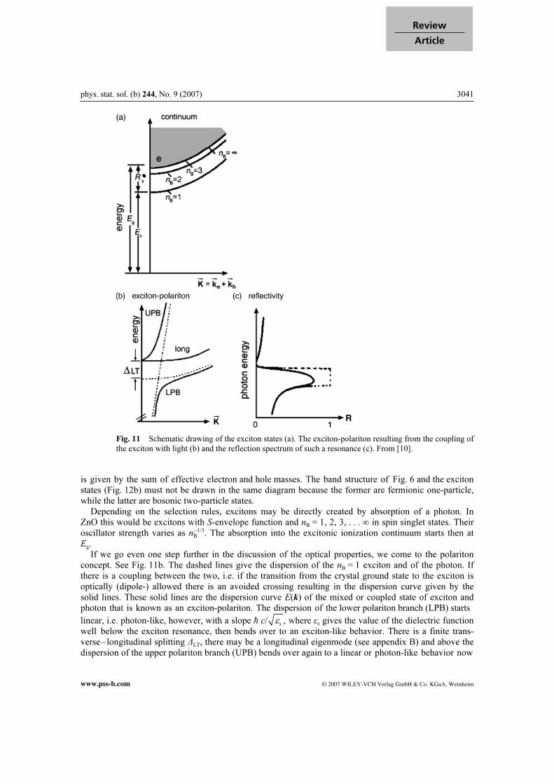
Fig. 11 Schematic drawing of the exciton states (a). The exciton-polariton resulting from the coupling of
the exciton with light (b) and the reflection spectrum of such a resonance (c). From [10]. is given by the sum of effective electron and hole masses. The band structure of Fig. 6 and the exciton states (Fig. 12b) must not be drawn in the same diagram because the former are fermionic one-particle, while the latter are bosonic two-particle states. Depending on the selection rules, excitons may be directly created by absorption of a photon. In ZnO this would be excitons with S-envelope function and nB = 1, 2, 3, . . . ∞ in spin singlet states. Their oscillator strength varies as nB
–1/3. The absorption into the excitonic ionization continuum starts then at Eg. If we go even one step further in the discussion of the optical properties, we come to the polariton concept. See Fig. 11b. The dashed lines give the dispersion of the nB = 1 exciton and of the photon. If there is a coupling between the two, i.e. if the transition from the crystal ground state to the exciton is optically (dipole-) allowed there is an avoided crossing resulting in the dispersion curve given by the solid lines. These solid lines are the dispersion curve E(k) of the mixed or coupled state of exciton and photon that is known as an exciton-polariton. The dispersion of the lower polariton branch (LPB) starts
linear, i.e. photon-like, however, with a slope ħ s
/ ,c ε where εs gives the value of the dielectric function well below the exciton resonance, then bends over to an exciton-like behavior. There is a finite trans-verse–longitudinal splitting ∆LT, there may be a longitudinal eigenmode (see appendix B) and above the dispersion of the upper polariton branch (UPB) bends over again to a linear or photon-like behavior now
3042 C. Klingshirn: ZnO: From basics towards applications
© 2007 WILEY-VCH Verlag GmbH & Co. KGaA, Weinheim www.pss-b.com
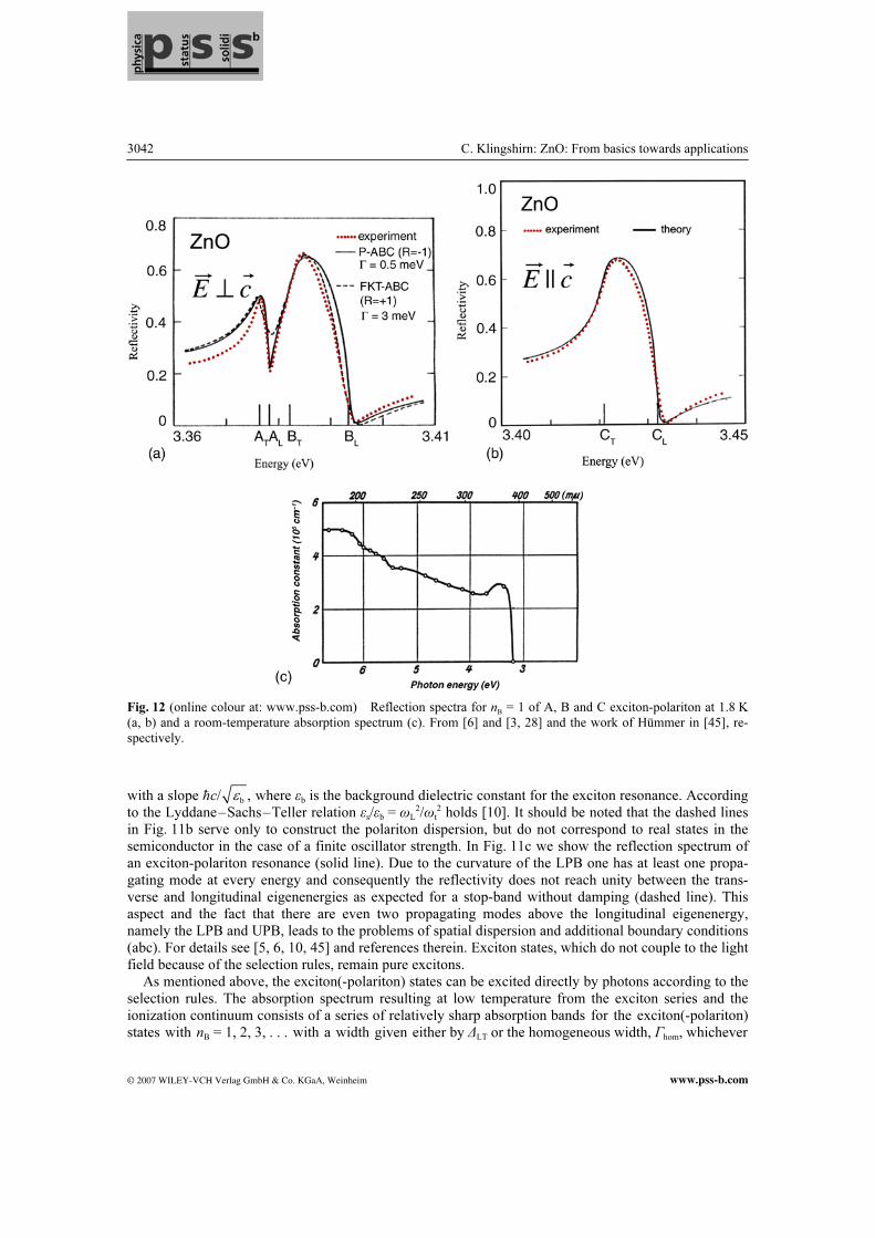
Fig. 12 (online colour at: www.pss-b.com) Reflection spectra for nB = 1 of A, B and C exciton-polariton at 1.8 K
(a, b) and a room-temperature absorption spectrum (c). From [6] and [3, 28] and the work of Hümmer in [45], re-
spectively.
with a slope ħb
/ ,c ε where εb is the background dielectric constant for the exciton resonance. According to the Lyddane–Sachs–Teller relation εs/εb = ωL
2/ωt2 holds [10]. It should be noted that the dashed lines
in Fig. 11b serve only to construct the polariton dispersion, but do not correspond to real states in the semiconductor in the case of a finite oscillator strength. In Fig. 11c we show the reflection spectrum of an exciton-polariton resonance (solid line). Due to the curvature of the LPB one has at least one propa-gating mode at every energy and consequently the reflectivity does not reach unity between the trans-verse and longitudinal eigenenergies as expected for a stop-band without damping (dashed line). This aspect and the fact that there are even two propagating modes above the longitudinal eigenenergy, namely the LPB and UPB, leads to the problems of spatial dispersion and additional boundary conditions (abc). For details see [5, 6, 10, 45] and references therein. Exciton states, which do not couple to the light field because of the selection rules, remain pure excitons. As mentioned above, the exciton(-polariton) states can be excited directly by photons according to the selection rules. The absorption spectrum resulting at low temperature from the exciton series and the ionization continuum consists of a series of relatively sharp absorption bands for the exciton(-polariton) states with nB = 1, 2, 3, . . . with a width given either by ∆LT or the homogeneous width, Гhom, whichever

phys. stat. sol. (b) 244, No. 9 (2007) 3043
www.pss-b.com © 2007 WILEY-VCH Verlag GmbH & Co. KGaA, Weinheim
Review
Article
is larger. It is followed by the absorption into the ionization continuum, starting at Eg. At higher tempera-tures there is scattering with phonons and a resulting stronger homogeneous broadening. It results in an exponential tail of the absorption that extends with increasing temperature more and more to lower ener-gies, following the Urbach–Martienssen rule [10]. In Fig. 12 we show various optical spectra of excitons in ZnO. Figure 12a and b shows the A, B, and C nB = 1 exciton resonances in reflection in their respec-tive polarization (see Figs. 11c and 6). At higher photon energies, not shown in Fig. 12a, b, one can see
Fig. 13 (online colour at: www.pss-b.com) Lumines-
cence spectra of ZnO for various temperatures (a)– (c), the
temperature dependence of the bandgap (d) and the homo-
geneous broadening of the exciton resonance (e). From
[74].
a) b)
c) d)
e)

3044 C. Klingshirn: ZnO: From basics towards applications
© 2007 WILEY-VCH Verlag GmbH & Co. KGaA, Weinheim www.pss-b.com
the reflection features for nB = 2, 3 [6, 45]. Figure 12c shows an early RT absorption spectrum of a thin ZnO film. The A and B exciton resonances merge to the peak around 3.3 eV. This peak is possibly the first observation of an excitonic feature in a semiconductor, but the author of [28] was evidently not aware of this fact. In [30] a similar procedure has been used as in [28] to prepare the ZnO film and a similar absorption spectrum has been observed, however, with a resolved double-peak structure with a splitting of 72 meV, which points to an LO-phonon satellite or an exciton–phonon bound state [10] rather than to the A–B splitting of 5 meV claimed in [30]. It should be noted that the absorption coeffi-cient reaches, in the excitonic ionization continuum of ZnO, already values beyond 105 cm–1. In the exci-ton resonances it is still higher and correspondingly difficult to measure, especially at low temperatures, where the broadening is smaller. Absorption spectra that show the well-resolved A and B Г5 states and the C Г1 state at lower temperature with an inhomogeneous width comparable to the respective values of ∆LT can be found, e.g. in [41, 42, 71] while the development of the Urbach tail with increasing tempera-ture is documented, e.g. in [28, 71, 72]. The spectra of the refractive index of this birefringent material can be found, e.g. in [72, 73]. In Fig. 13a–c we show the excitonic luminescence spectra of ZnO for various temperatures. One sees the (broadened) peak of the A and B exciton-polaritons at 110 K around 3.37 eV and their LO-phonon replica around 3.30 eV and 3.225 eV. Note that the correct LO-phonon energy of 72 meV appears be-tween the zero-phonon band and the first LO-phonon replica in contrast to other claims in some of the references [75b]. With increasing temperature the homogeneous broadening increases, too, resulting at RT (and above) in a broad, unstructured emission band. This development of the luminescence is seen in bulk samples, epitaxial layers, or nanorods. It should be noted that its RT peak is not identical with the exciton energy. The discrepancy between the measured spectrum and the model at higher temperatures results from reabsorption. Investigation of absorption and luminescence allow determination of the temperature dependence of the free exciton resonances (and also of the bandgap). In Fig. 13d we show this dependence up to 800 K. The damping deduced from the line shape fit of both the zero-phonon emission and its LO-phonon rep-lica shows that the homogeneous broadening of the exciton resonance increases from values below 1 meV at 5 K to 20 meV (HWHM) at RT [74], see Fig. 13e. The formula used to describe the temperature of homogeneous broadening Г [74, 75a] is
1
0( ) (exp / 1)T T k TβΓ Γ α β Ω -
= + + - . (8)
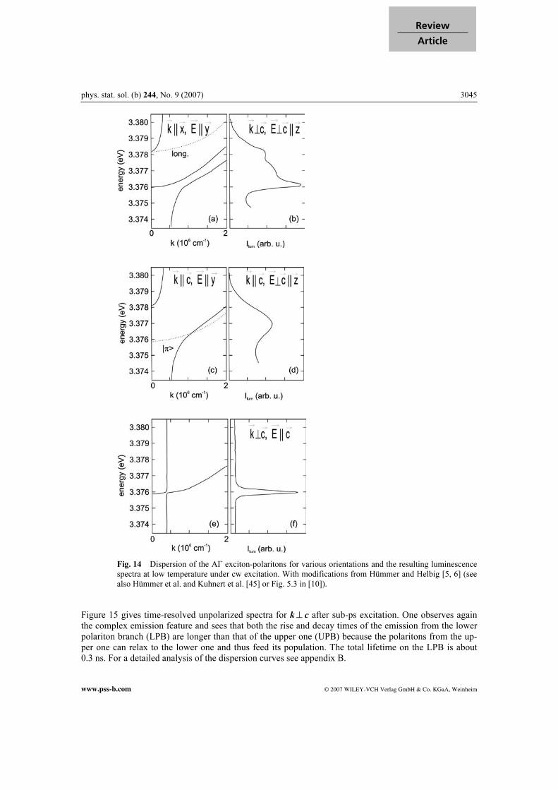
Г0 is the low-temperature value, which is in agreement with the analysis of low-temperature reflection spectra below or around 1 meV (see Fig. 12a and b and [45]). The parameters α and β describe the coupling to acoustic and optic phonons, respectively. The fit in [74] gives α = (0.016 ± 0.013) meV/K and β = (47 ± 12) meV. The quantity ћΩ is an average over the optical phonon energies with ћΩ = (33 ± 7.5) meV. Compare to Table 1. In [75a] the same formula has been used but with unphysi-cally high numerical values. For Г0 partly the value of the half-width of the low-temperature absorption features of A and B Г5 excitons has been used, which is close to ∆LT but describes rather an inhomo-geneous broadening. For β, values have been used in the range of several hundred meV, which result in values of Г (300 K) around 1 eV for A and B excitons, respectively. These values would exclude any observation of excitonic features already below RT and even more so at RT and above in strong contrast to experiment. In Figs. 14 and 15 we show finally details of the free exciton luminescences under cw and pulsed excitation, respectively. Figure 14 gives the exciton-polariton dispersion and luminescence for various orientations. For k^ c there is a k-linear term for the A valence band (see Fig. 6), which mixes the for-bidden A Г1 ≈ Г2 spin-triplet states with the allowed A Г5 spin singlet state and thus causes the interme-diate polariton branch of Fig. 14a. The complex polariton dispersion shows up in the complex lumines-cence spectrum of Fig. 14b. For k || c this term is absent and both the polariton dispersion and the lumi-nescence are much simpler and smooth (Fig. 14c and d). For E || c the A Г1 exciton is dipole allowed but spin-flip forbidden resulting in a small oscillator strength only and a narrower emission (Fig. 14e and f).
phys. stat. sol. (b) 244, No. 9 (2007) 3045
www.pss-b.com © 2007 WILEY-VCH Verlag GmbH & Co. KGaA, Weinheim
Review
Article
Fig. 14 Dispersion of the AГ exciton-polaritons for various orientations and the resulting luminescence
spectra at low temperature under cw excitation. With modifications from Hümmer and Helbig [5, 6] (see
also Hümmer et al. and Kuhnert et al. [45] or Fig. 5.3 in [10]).
Figure 15 gives time-resolved unpolarized spectra for k^ c after sub-ps excitation. One observes again the complex emission feature and sees that both the rise and decay times of the emission from the lower polariton branch (LPB) are longer than that of the upper one (UPB) because the polaritons from the up-per one can relax to the lower one and thus feed its population. The total lifetime on the LPB is about 0.3 ns. For a detailed analysis of the dispersion curves see appendix B.

3046 C. Klingshirn: ZnO: From basics towards applications
© 2007 WILEY-VCH Verlag GmbH & Co. KGaA, Weinheim www.pss-b.com
3.375 3.376 3.377 3.378 3.379 3.380
UPBLPB
PLIn
tens
ity(a
rb.u
.)
Photon Energy(eV)
0 ps15 ps39 ps208 ps437 ps
2 meV
0 100 200 300 400 500
UPBLPB
PL
Inte
nsi
ty(n
orm
.)
Time (ps)a) b)
Fig. 15 (online colour at: www.pss-b.com) Unpolarized emission spectra for k perpendicular to c for different time
delays after a sub-ps excitation pulse (a) and the rise and decay dynamics of the low- and high-energy peaks (b).
From [12, 77]. To conclude this section two further details should be mentioned. So-called mixed-mode polaritons exist for the orientation E in the plane of k and c and the angle (k, c) ≠ 0 or π/2. They correspond to the extraordinary beam of crystal optics in this birefringent and dichroitic material [6, 10, 76]. For most of the bulk excitations, like phonons or plasmons, there exists a surface or interface mode, which can propagate only along the boundary with amplitudes decaying exponentially on both sides [10]. This is also the case for exciton-polaritons. The dispersion of surface exciton-polaritons E(k||) for the interface between a semiconductor, here ZnO, and vacuum (or air) is situated in the spectral region be-tween the LPB and the longitudinal one and on the rhs of the photon dispersion (see Fig. 11b). This placement forbids the decay of the surface exciton-polariton into the sample, because there is no propa-gating mode and into the vacuum side, because
k|| > kvac = vac
2π
c
ω
λ= , (8a)
because the parallel component of k is conserved at a plane interface. Coupling to the surface exciton-polariton is possible, e.g. via a prism coupler using the evanescent wave at the base of the prism in a configuration of attenuated total internal reflection (ATR) or by pro-ducing an artificial periodicity or grating on the surface of the sample with period λg resulting in a con-servation of k|| only for modulo integer multiples of 2π/λg i.e.
k|| → k|| + n2π/λg, n = 0, ±1, ±2, . . . (8b)
For more details on this topic see [10, 78]. In Fig. 13a one observes for 110 K sharp emission peaks around 3.35 eV. This is the reminder of bound-exciton complexes described in the following section.
9.2 Bound-exciton complexes
In the preceding section we treated the optical properties of free, intrinsic exciton(-polariton)s, which are characterized by a k vector and a dispersion relation E(k) and that can move freely through the crystal and are subject to scattering processes, e.g. with phonons or structural defects. Furthermore, excitons can be bound to some center or defect, like ionized or neutral donors (D+, D0) or neutral acceptors (A0) form-
phys. stat. sol. (b) 244, No. 9 (2007) 3047
www.pss-b.com © 2007 WILEY-VCH Verlag GmbH & Co. KGaA, Weinheim
Review
Article
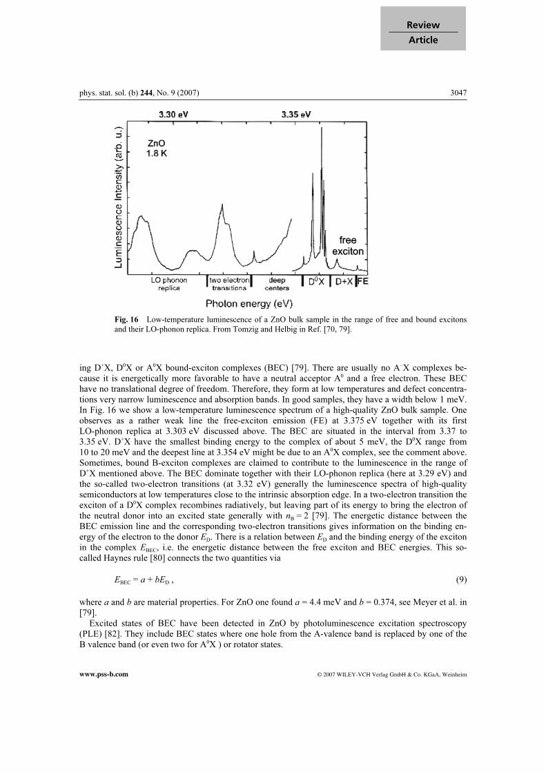
Fig. 16 Low-temperature luminescence of a ZnO bulk sample in the range of free and bound excitons
and their LO-phonon replica. From Tomzig and Helbig in Ref. [70, 79].
ing D+X, D0X or A0X bound-exciton complexes (BEC) [79]. There are usually no A–X complexes be-cause it is energetically more favorable to have a neutral acceptor A0 and a free electron. These BEC have no translational degree of freedom. Therefore, they form at low temperatures and defect concentra-tions very narrow luminescence and absorption bands. In good samples, they have a width below 1 meV. In Fig. 16 we show a low-temperature luminescence spectrum of a high-quality ZnO bulk sample. One observes as a rather weak line the free-exciton emission (FE) at 3.375 eV together with its first LO-phonon replica at 3.303 eV discussed above. The BEC are situated in the interval from 3.37 to 3.35 eV. D+X have the smallest binding energy to the complex of about 5 meV, the D0X range from 10 to 20 meV and the deepest line at 3.354 eV might be due to an A0X complex, see the comment above. Sometimes, bound B-exciton complexes are claimed to contribute to the luminescence in the range of D+X mentioned above. The BEC dominate together with their LO-phonon replica (here at 3.29 eV) and the so-called two-electron transitions (at 3.32 eV) generally the luminescence spectra of high-quality semiconductors at low temperatures close to the intrinsic absorption edge. In a two-electron transition the exciton of a D0X complex recombines radiatively, but leaving part of its energy to bring the electron of the neutral donor into an excited state generally with nB = 2 [79]. The energetic distance between the BEC emission line and the corresponding two-electron transitions gives information on the binding en-ergy of the electron to the donor ED. There is a relation between ED and the binding energy of the exciton in the complex EBEC, i.e. the energetic distance between the free exciton and BEC energies. This so-called Haynes rule [80] connects the two quantities via
EBEC = a + bED , (9)
where a and b are material properties. For ZnO one found a = 4.4 meV and b = 0.374, see Meyer et al. in [79]. Excited states of BEC have been detected in ZnO by photoluminescence excitation spectroscopy (PLE) [82]. They include BEC states where one hole from the A-valence band is replaced by one of the B valence band (or even two for A0X ) or rotator states.

3048 C. Klingshirn: ZnO: From basics towards applications
© 2007 WILEY-VCH Verlag GmbH & Co. KGaA, Weinheim www.pss-b.com
With increasing temperature the excitons are more and more thermally released from their centers and tend to disappear around 80 K in ZnO (see Fig. 13a). There are also excitons bound to defects at or close to the surfaces [81]. These states are sometimes called surface excitons and must not be confused with the intrinsic surface exciton(-polariton)s above. Evidently their importance increases with increasing surface to volume ratio. Consequently, they may dominate the emission, e.g. in ZnO powders [81]. The lifetime of free and bound excitons is, in ZnO as in other direct wide gap semiconductors, typi-cally in the range of 0.1 to 1 ns and is especially for the free excitons generally determined by nonradia-tive recombination processes. These statements can be deduced from the fact that the absolute external luminescence yield of the free and bound excitons including their LO-phonon replica has values up to 0.15 even in high-quality samples considerably below unity [66].
10 High-excitation effects
When one increases the densities of excitons and/or free carriers in a semiconductor, e.g. by excitation with short and intense laser pulses or by carrier injection in a forward-biased p(i)n-junction new phe-nomena appear in the optical spectra. The scenario was developed in the 1980s. It is didactically very valuable and we first outline it here briefly and then add, in Section 11, some modifications necessary from the present point of view. As we shall also see in Section 11, many of the effects introduced here are capable of showing stimulated emis-sion. In Fig. 17 we show schematically a sample and the processes that occur with increasing generation rate or excitation intensity. In the low-density limit there are (e.g. under quasistationary excitation condi-tions) free excitons, at low temperature also bound-exciton complexes and at higher temperatures also
Fig. 17 Schematic drawing of the scenario in a semiconductor with increasing excitation. According to [10].
phys. stat. sol. (b) 244, No. 9 (2007) 3049
www.pss-b.com © 2007 WILEY-VCH Verlag GmbH & Co. KGaA, Weinheim
Review
Article
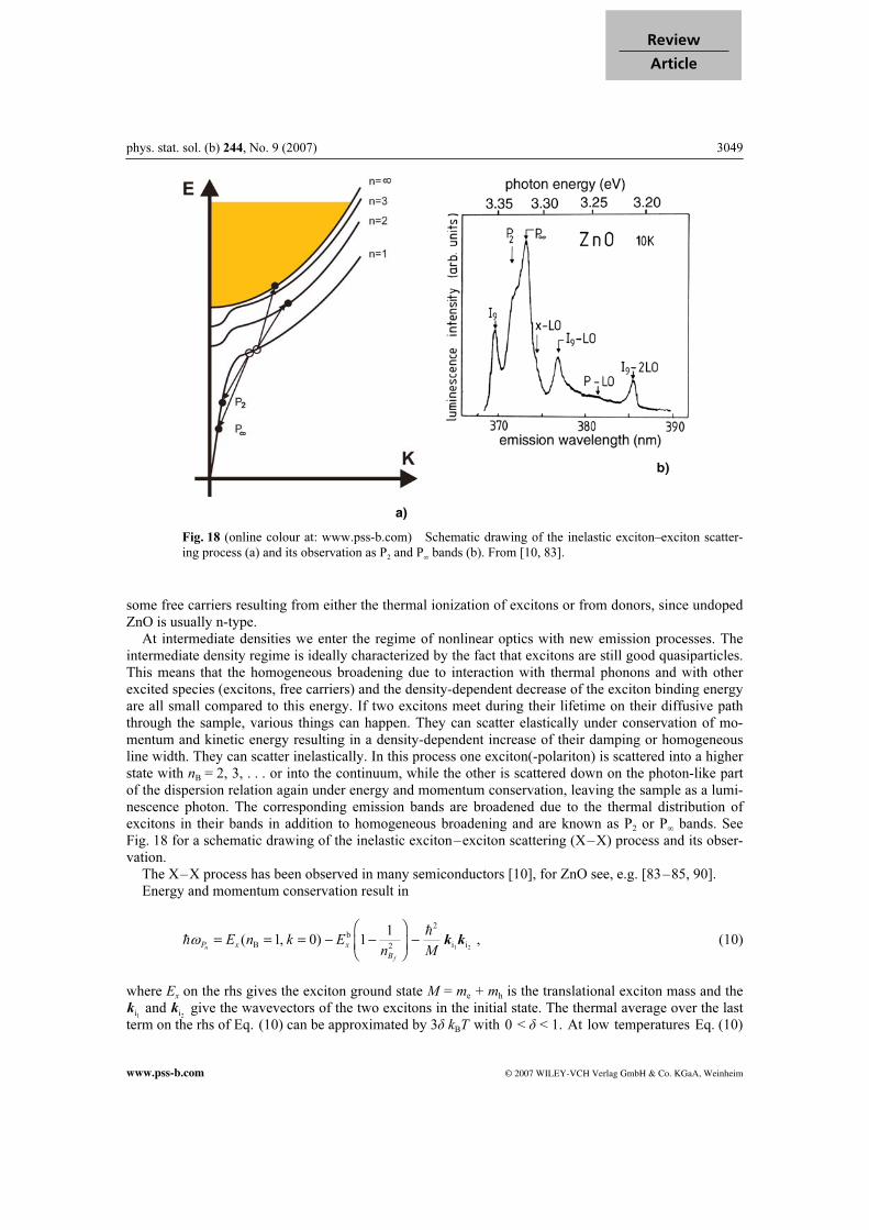
a)
Fig. 18 (online colour at: www.pss-b.com) Schematic drawing of the inelastic exciton–exciton scatter-
ing process (a) and its observation as P2 and P
∞ bands (b). From [10, 83].
some free carriers resulting from either the thermal ionization of excitons or from donors, since undoped ZnO is usually n-type. At intermediate densities we enter the regime of nonlinear optics with new emission processes. The intermediate density regime is ideally characterized by the fact that excitons are still good quasiparticles. This means that the homogeneous broadening due to interaction with thermal phonons and with other excited species (excitons, free carriers) and the density-dependent decrease of the exciton binding energy are all small compared to this energy. If two excitons meet during their lifetime on their diffusive path through the sample, various things can happen. They can scatter elastically under conservation of mo-mentum and kinetic energy resulting in a density-dependent increase of their damping or homogeneous line width. They can scatter inelastically. In this process one exciton(-polariton) is scattered into a higher state with nB = 2, 3, . . . or into the continuum, while the other is scattered down on the photon-like part of the dispersion relation again under energy and momentum conservation, leaving the sample as a lumi-nescence photon. The corresponding emission bands are broadened due to the thermal distribution of excitons in their bands in addition to homogeneous broadening and are known as P2 or P∞ bands. See Fig. 18 for a schematic drawing of the inelastic exciton–exciton scattering (X–X) process and its obser-vation. The X–X process has been observed in many semiconductors [10], for ZnO see, e.g. [83–85, 90]. Energy and momentum conservation result in
1 2
2
b
B i i2
1( 1, 0) 1
n
f
P x x
B
E n k En M
ω
Ê ˆ= = = - - -Á ˜Ë ¯
k k , (10)
where Ex on the rhs gives the exciton ground state M = me + mh is the translational exciton mass and the
1ik and
2ik give the wavevectors of the two excitons in the initial state. The thermal average over the last
term on the rhs of Eq. (10) can be approximated by 3δ kBT with 0 < δ < 1. At low temperatures Eq. (10)

3050 C. Klingshirn: ZnO: From basics towards applications
© 2007 WILEY-VCH Verlag GmbH & Co. KGaA, Weinheim www.pss-b.com
results in values around 3.32 eV for P∞. In Fig. 19 we show normalized emission spectra for low tem-perature and increasing excitation density of a 0.4 µm thick epitaxial ZnO layer grown by MOVPE on Al2O3(111) with a GaN buffer layer. The lowest trace has been taken under cw excitation with a HeCd laser (ћωexc = 3.81 eV) and shows essentially the dominant BEC luminescence (see Section 9.2). At in-termediate pump powers the P-band appears around 3.32 eV. Another process which can occur at low temperatures during the collision of two excitons is the for-mation of an excitonic molecule or biexciton in analogy to the formation of a H2 or a positronium mole-cule. The binding energy Eb
xx of the biexciton in ZnO relative to two free excitons is around 15 meV [86].
This binding energy must be dissipated in the biexcitonic formation process from two free excitons in the form of phonon (or photon) emission. Since Eb
xx is larger than the splitting of the A and B VB, one also
observed in ZnO biexciton states that contain one hole from the A and one from the B VB or even two B holes. The binding energies of these states are similar relative to the two involved excitons [12, 86]. See also Appendix C. Biexcitons have also been observed in ZnO QW [12, 86]. The binding energies of both excitons and biexcitons are enhanced in QW due to the spatial confinement in one direction. Apart from the formation in a collision between two free excitons, biexcitons can be created directly by two photon absorption (see the work by Hvam et al. in [86]) or by the conversion of an exciton into a biexciton by absorption of one photon [7, 8, 10]. This latter process is called induced absorption. It oc- curs at a photon energy given by
2 2
b i
4ia x xx
kE E
Mω
= - - , (11)
Fig. 19 Normalized luminescence spectra of a
ZnO epitaxial layer at low temperature and for
increasing excitation. According to [85].
Fig. 20 Temperature dependence of the transverse
nB = 1 Г
5 A and B excitons and of various emission
maxima. References [4–8, 10, 22] in the figure corre-
spond to Refs. [92–98] of this paper. From [74, 84, 87].
phys. stat. sol. (b) 244, No. 9 (2007) 3051
www.pss-b.com © 2007 WILEY-VCH Verlag GmbH & Co. KGaA, Weinheim
Review
Article
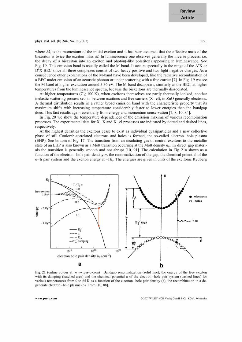
where ћki is the momentum of the initial exciton and it has been assumed that the effective mass of the biexciton is twice the exciton mass M. In luminescence one observes generally the inverse process, i.e. the decay of a biexciton into an exciton and photon(-like polariton) appearing in luminescence. See Fig. 19. This emission band is usually called the M-band. It occurs spectrally in the range of the A0X or D0X BEC since all three complexes consist of two heavy positive and two light negative charges. As a consequence other explanations of the M-band have been developed, like the radiative recombination of a BEC under emission of an acoustic phonon or under scattering with a free carrier [7]. In Fig. 19 we see the M-band at higher excitation around 3.36 eV. The M-band disappears, similarly as the BEC, at higher temperatures from the luminescence spectra, because the biexcitons are thermally dissociated. At higher temperatures (T ≥ 100 K), when excitons themselves are partly thermally ionized, another inelastic scattering process sets in between excitons and free carriers (X–el), in ZnO generally electrons. A thermal distribution results in a rather broad emission band with the characteristic property that its maximum shifts with increasing temperature considerably faster to lower energies than the bandgap does. This fact results again essentially from energy and momentum conservation [7, 8, 10, 84]. In Fig. 20 we show the temperature dependences of the emission maxima of various recombination processes. The experimental data for X–X and X–el processes are indicated by dotted and dashed lines, respectively. At the highest densities the excitons cease to exist as individual quasiparticles and a new collective phase of still Coulomb-correlated electrons and holes is formed, the so-called electron–hole plasma (EHP). See bottom of Fig. 17. The transition from an insulating gas of neutral excitons to the metallic state of an EHP is also known as a Mott transition occurring at the Mott density nM. In direct gap materi-als the transition is generally smooth and not abrupt [10, 91]. The calculation in Fig. 21a shows as a function of the electron–hole pair density nP the renormalization of the gap, the chemical potential of the e–h pair system and the exciton energy at –1Ry. The energies are given in units of the excitonic Rydberg
Fig. 21 (online colour at: www.pss-b.com) Bandgap renormalization (solid line), the energy of the free exciton
with its damping (hatched area) and the chemical potential µ of the electron–hole pair system (dashed lines) for
various temperatures from 0 to 65 K as a function of the electron–hole pair density (a), the recombination in a de-
generate electron–hole plasma (b). From [10, 88].
3052 C. Klingshirn: ZnO: From basics towards applications
© 2007 WILEY-VCH Verlag GmbH & Co. KGaA, Weinheim www.pss-b.com
or binding energy R*y = Exb. The calculation is for CdS. The results are similar for ZnO, but nM is rather at
np = 3 to 5 × 1017 cm–3 instead of 8 × 1016 cm–3 [74, 91]. See below for the deduction of the numbers for ZnO. The bandgap renormalization (BGR) is caused by the following many-particle effects. The width of the forbidden gap is a monotonously decreasing function with increasing electron–hole pair density nP, due to exchange and correlation effects. The binding energy of the exciton Ex
b(nP) also decreases with increasing nP, because the Coulomb attraction of electron and hole is increasingly screened by the addi-tional electron–hole pairs and vanishes at nM. As a consequence the absolute energy of the exciton Ex = Eg(nP) – Ex
b(nP) is almost constant but its damping increases with nP. In ZnO the nM is around 3 to 5 × 1017 cm–3, and is only weakly dependent on temperature [74]. In Fig. 21a we show this behavior schematically. In the upmost spectra of Fig. 19 emission from an EHP is seen. The increasing redshift of the emission with increasing excitation reflects the decrease of Eg′ with increasing nP and the narrowing of the emission band indicates the onset of stimulated emission. This aspect brings us to the topic of the next section.
11 Stimulated emission
We treat in this section first the basic concepts of stimulated emission in ZnO and then we refine the picture as announced in Section 10.
11.1 Basic concepts
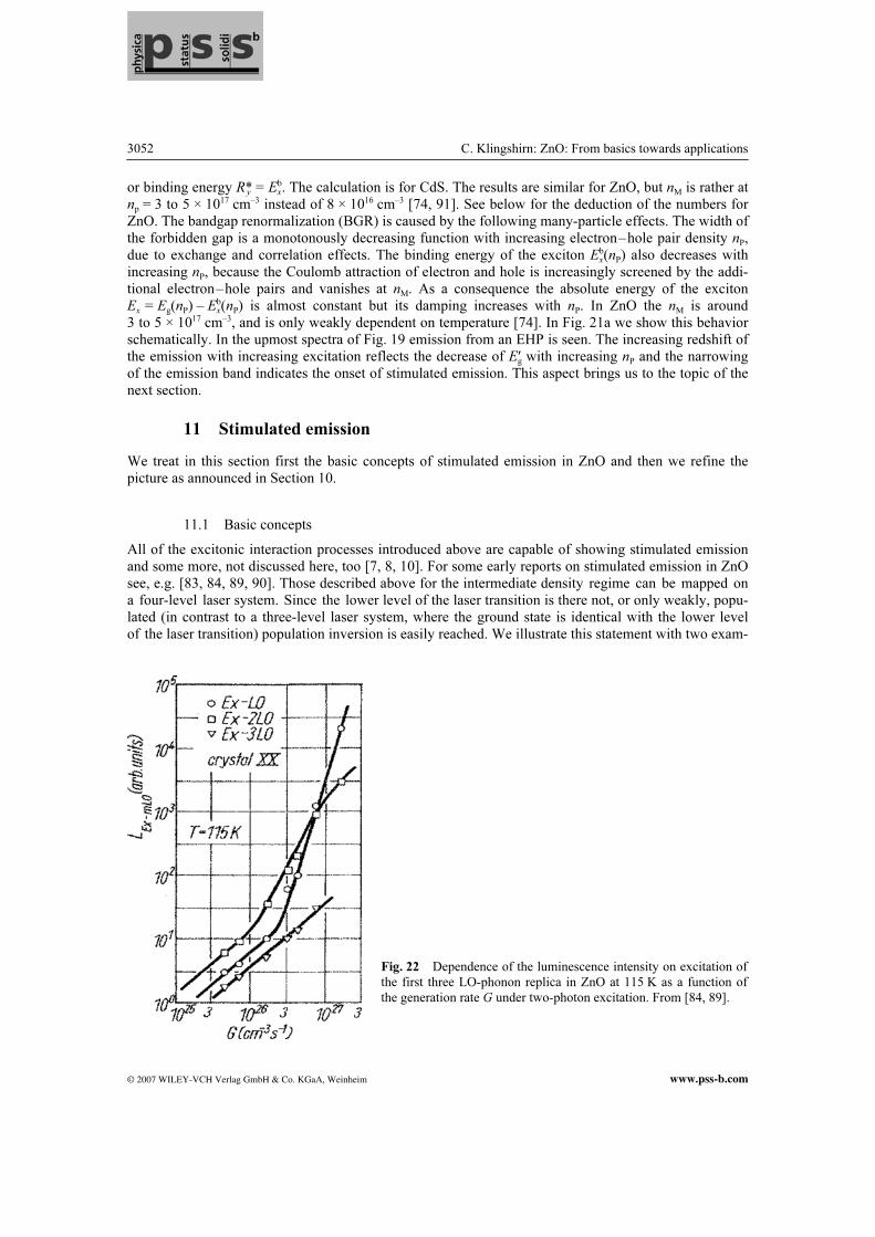
All of the excitonic interaction processes introduced above are capable of showing stimulated emission and some more, not discussed here, too [7, 8, 10]. For some early reports on stimulated emission in ZnO see, e.g. [83, 84, 89, 90]. Those described above for the intermediate density regime can be mapped on a four-level laser system. Since the lower level of the laser transition is there not, or only weakly, popu-lated (in contrast to a three-level laser system, where the ground state is identical with the lower level of the laser transition) population inversion is easily reached. We illustrate this statement with two exam-
Fig. 22 Dependence of the luminescence intensity on excitation of
the first three LO-phonon replica in ZnO at 115 K as a function of
the generation rate G under two-photon excitation. From [84, 89].
phys. stat. sol. (b) 244, No. 9 (2007) 3053
www.pss-b.com © 2007 WILEY-VCH Verlag GmbH & Co. KGaA, Weinheim
Review
Article
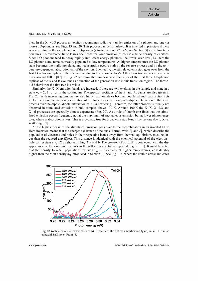
ples. In the X–nLO process an exciton recombines radiatively under emission of a photon and one (or more) LO-phonons, see Figs. 13 and 20. This process can be stimulated. It is inverted in principle if there is one exciton in the sample and no LO-phonon (situated around 72 meV, see Section 3) i.e. at low tem-peratures. To overcome finite losses one needs for laser emission of course a finite density of excitons. Since LO-phonons tend to decay rapidly into lower energy phonons, the lower laser level, i.e. here the LO-phonon state, remains weakly populated at low temperatures. At higher temperatures the LO-phonon state becomes thermally populated and reabsorption occurs both by the reverse process and by the tem-perature-dependent absorption tail of the exciton. Eventually, the stimulated emission goes over from the first LO-phonon replica to the second one due to lower losses. In ZnO this transition occurs at tempera-tures around 100 K [89]. In Fig. 22 we show the luminescence intensities of the first three LO-phonon replicas of the A and B excitons as a function of the generation rate in this transition region. The thresh-old behavior of the first two is obvious. Similarly, the X–X emission bands are inverted, if there are two excitons in the sample and none in a state nB = 2, 3 . . . or in the continuum. The spectral positions of the P2 and P∞ bands are also given in Fig. 20. With increasing temperature also higher exciton states become populated and reabsorption sets in. Furthermore the increasing ionization of excitons favors the monopole–dipole interaction of the X–el process over the dipole–dipole interaction of X–X scattering. Therefore, the latter process is usually not observed in stimulated emission in bulk samples above 100 K. Around 100 K the X–X, X–LO and X–el processes are spectrally almost degenerate (Fig. 20). As a rule of thumb one finds that the stimu-lated emission occurs frequently not at the maximum of spontaneous emission but at lower photon ener-gies, where reabsorption is less. This is especially true for broad emission bands like the one due to X–el scattering [87]. At the highest densities the stimulated emission goes over to the recombination in an inverted EHP. Here inversion means that the energetic distance of the quasi-Fermi levels Ee
F and EhF, which describe the
population of electrons and holes in their respective bands away from thermal equilibrium, must be lar-ger than the reduced gap E′g(np). This distance is identical with the chemical potential of the electron–hole pair system µ(np, T) as shown in Fig. 21a and b. The creation of an EHP is connected with the dis-appearance of the excitonic features in the reflection spectra as reported, e.g. in [91]. It must be noted that the density to reach population inversion npi is, especially at higher temperatures, considerably higher than the Mott density nM introduced in Section 10. See Fig. 21a, where the double arrow indicates
3.20 3.22 3.24 3.26 3.28 3.30 3.32 3.340
50
100
150
200
250
300T=10K
gai
n(c
m-1)
Photon energy (eV)
4600 kW/cm2
2600 kW/cm2
1400 kW/cm2
825 kW/cm2
570 kW/cm2
325 kW/cm2
Fig. 23 (online colour at: www.pss-b.com) Spectra of the optical amplification (gain) in an EHP in an
epitaxial ZnO layer. From [85].

3054 C. Klingshirn: ZnO: From basics towards applications
© 2007 WILEY-VCH Verlag GmbH & Co. KGaA, Weinheim www.pss-b.com
the spectral interval in which optical amplification occurs. See also the bar on the lhs of Figs. 20 and 23, where the gain has been deduced from a variation of the excitation stripe length. For older data on EHP gain spectra in ZnO see [91]. The answer to the question which of the above laser processes reaches, with increasing pump power, the laser threshold first depends on various parameters like the sample temperature, the loss rate that has to be overcome, the doping level and others. Most of the presently available commercial laser diodes work on the stimulated emission from an inverted EHP.
11.2 Refined modelling
The processes introduced in Section 10 and above “for didactical purposes” have their place. The exci-tonic processes are realized for densities np considerably below nM and for temperatures where the ho-mogeneous broadening is small compared to Eb
X, i.e. typically below RT. For possible future application of ZnO as a material for laser diodes (LD) the processes at or even above RT are most relevant. Conse-quently, many research groups concentrate on this temperature range and investigate preferentially epi-taxial ZnO layers. Surprisingly, the observed stimulated emission is attributed either to the X–X process, partly specifying even P2 or P∞ or to recombination in an inverted EHP. For some examples of these statements see Fig. 20 and references therein, where the open symbols stand for the claim of X–X scat-tering and the closed ones for EHP recombination. It is an experimental finding that all RT data for stimulated emission in ZnO concentrate in the spectral range (3.1 ± 0.1) eV, irrespective of the claimed recombination process. The author feels that these statements for the origin of stimulated emission are, in many cases, not well justified. To justify this statement, we show in Fig. 24a the reduction of the gap normalized by R*y as a function of the dimensionless quantity rs
rs = 1/33
B P4π
3
a n
-
Ê ˆÁ ˜Ë ¯
, (12a)
which compares the volume of an exciton with radius aB to nP. There are two universal calculations by Vashista and Kalia and by Zimmermann [88] and experimental data for various II–VI compounds. One
Fig. 24 Renormalization of the gap in an EHP in units of the R*y as a function of rs. Solid and dashed lines by Vash-
ista and Kalia and by Zimmermann, respectively [88], together with experimental data for various II–VI semicon-
ductors from [10] (a) and the renormalization ∆Eg of Eg, the exciton energy with its homogeneous width indicated by
the shaded area and the chemical potential µ in ZnO at RT as a function of nP (b). From [74].
a) b)

phys. stat. sol. (b) 244, No. 9 (2007) 3055
www.pss-b.com © 2007 WILEY-VCH Verlag GmbH & Co. KGaA, Weinheim
Review
Article
sees that the experimental data are slightly below the calculation. With the knowledge (from Fig. 21a) that the absolute exciton energy is almost independent of rs, we see that nM is reached for
rs(nM) ≈ 4 . (12b)
Consequently, the frequently used rule of thumb [10]
nMa3B = 1 , (12c)
overestimates nM by about two orders of magnitude. In Fig. 24b we show values calculated for ZnO at RT on the basis of data in Fig. 24a. The dashed line gives the bandgap renormalization as a function of nP, according to Vashista and Kalia in Fig. 24a and the solid one gives a fit with their formula to the experimental data in Fig. 24a. The shaded area gives the homogeneous width of the exciton at RT. See Fig. 13e. The two curves result in nM = 3 or 5 – 1017 cm–3, but it is obvious that the exciton is getting soft already at considerably lower densities. The X–X process according to Eq. (10) with the unperturbed exciton binding energy of 60 meV can be ruled out at RT already for densities below 1017 cm–3. On the other hand, the chemical potential µ(nP, 300 K) crosses the reduced gap only for densities around ni = 5 × 1018 cm–3, ruling out stimulated emission from direct re-combination in the EHP for lower densities. The crucial point is now that the ns or ps pump- or excita-tion intensities (for ns pulses typically in the range from below 100 kW/cm2 up to 1 MW/cm2) result in electron–hole pair densities between a few times 1017 to 1019 cm–3 using realistic values of lifetime, penetration depth of the exciting light and diffusion length of the excited carriers [9, 74, 87] where the excitons are no longer good quasiparticles and the band-to-band transition in the EHP is not yet in-verted. Furthermore, the large shift of the emission band denoted by the solid stars relative to the bandgap at 550 K in Fig. 20 would require a correspondingly large bandgap renormalization of at least 300 meV resulting in values npi(550 K) > 1020 cm–3, which are above the damage threshold of the sample under ns-pulse excitation and are incompatible with the excitation conditions. Consequently we have to look for alternative processes to explain the (above-) RT stimulated emis-sion in ZnO. The processes that we suggest [74] are in some sense modifications of the ones introduced above. One is an inelastic scattering of an essentially unbound electron–hole pair in an EHP and a free carrier resulting in a photon and the free carrier scattered to higher kinetic energy. This process allows us to explain optical gain in an EHP for densities below npi. Energy and momentum conservation result also for this process in an enhanced redshift with temperature and the experimental data given by the solid stars in Fig. 20 extrapolate indeed the ones for X–el scattering from lower temperatures. This is also true for the data for ZnO QW reported in [98]. Furthermore, it should be noted that the densities reached or claimed in older work at lower temperatures might have been in some cases also close to nM, favoring the (e–h)–el process over the X–el process [83, 84, 89, 90]. For the next process it should be noted that in the carrier gas of electrons and holes of an EHP a new quasiparticle exists, the plasmon at energy ћωPl. This plasmon is a longitudinal eigenmode (the transverse plasma frequency is zero), which interacts strongly with the optical phonons resulting in yet another quasiparticle, the plasmon–phonon mixed-state quanta [10]. This coupling effect is espe-cially pronounced if ћωP is approximately equal to or even larger than ћωLO. In ZnO this is the case for np ≈ 3 × 1018 cm–3. Therefore, we introduce as another process to explain (above-) RT lasing the recom-bination of an e–h pair in an EHP under emission of one or two plasmon–phonon mixed-state quanta. Since the reduced gap coincides around nM with the energy of the exciton at low densities, this process leads at RT also to emission in the above-mentioned spectral interval but will shift less to lower energies with increasing temperature. See the open stars in Fig. 20. We think that these two processes are indeed good candidates to explain stimulated emission at RT and above and partly also below. It is now a chal-lenge to theory to model these processes quantitatively and by doing so to verify or falsify the above models. A further aspect, which comes into play both in alloys and/or in quantum wells, are localized exciton states, which may also result in stimulated emission up to relatively high temperatures [10, 98].

3056 C. Klingshirn: ZnO: From basics towards applications
© 2007 WILEY-VCH Verlag GmbH & Co. KGaA, Weinheim www.pss-b.com
11.3 Lasing in ZnO nanorods and powders
To conclude this part on stimulated emission and lasing we mention that these phenomena have not only been observed in bulk samples, epitaxial layers or quantum wells as discussed above, but also in ZnO nanorods and powders. For stimulated emission in nanorods see, e.g. [99, 101]. The discussion concern-ing the laser processes from Section 11.2 also applies here. In addition, the emission is strongly influ-enced by the cavity modes. Whispering-gallery modes in nanorods have been investigated without laser emission in the broad green luminescence band [100] mentioned in Section 7. The transverse and longi-tudinal mode pattern of nanorods has been calculated in [101] and it has been found there that the mode pattern has a strong influence on the photon energy at which laser emission occurs. Usually one does not expect lasing in disordered media but one expects the combination of a resonator and an active medium. Recently it has been shown, however, that so-called random lasing can occur in powders, e.g. of ZnO [102]. The multiple scattering from the grains of the powder keeps the light longer in the pumped volume. This effect may be even enhanced by weak localization of light in the random medium (i.e. the powder) by enhanced backscattering. Lasing of ZnO in photonic crystals has also been reported recently. See, e.g. the work by Scharrer in [102].
12 Applications of ZnO
ZnO production is approximately 105 tons per year. Zn is evidently much more available (and less poi-sonous!) than, e.g., Ga. In the following, we give first a list of a variety of existing applications and then an outlook or vision for future applications, especially in the field of optoelectronics, including junctions.
12.1 Existing applications
A large fraction of the ZnO is used in the rubber and concrete industries [2]. ZnO is an important addi-tive to the rubber of tires of cars. It has a positive influence on the vulcanization process and it improves considerably the heat conductivity that is crucial to dissipate the heat produced in the rubber of the tire by the deformation when it rolls along the street. In concrete an admixture of ZnO allows increased proc-essing time and improves the resistance of the concrete against water. Other applications concern medi-cine or cosmetics. ZnO is used as a UV-blocker in sun lotions or as an additive to human and animal food. Furthermore, it is used as one component of mixed oxide varistors, devices that allow voltage lim-iting [103].
12.2 Forthcoming applications and visions
Since the surface conductivity of ZnO can be strongly influenced by various gases, it is used as a gas sensor [104]. The pointed tips of single crystals and nanorods (Figs. 3 and 5) result in a strong enhancement of an electric field. Therefore they can be used as field emitters [105]. Due to its wide bandgap, ZnO is transparent in the visible part of the electromagnetic spectrum. Highly n-doped ZnO:Al can therefore be and partly is already used as a transparent conducting oxide (TCO) [106]. The constituents Zn and Al are much cheaper and less poisonous compared to the generally used indium-tin oxide (ITO). One application is as the front contact to solar cells, which avoids the shadow effect necessarily connected with metal finger contacts. Another application is as the front con-tact of liquid crystal displays [107], still another of ZnO:Al is in the production of energy-saving or heat-protecting windows. For the properties of ZnO as a UV-sensitive and solar-blind photodetector see [108] and for its hard-ness against high-energy radiation see [109]. Furthermore, transparent thin-film transistors (TTFT) can be produced with ZnO. In the version of field-effect transistors they even do not need a p–n junction [110]. Some of the field-effect transistors
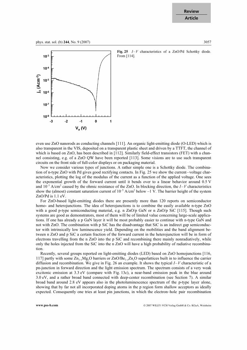
phys. stat. sol. (b) 244, No. 9 (2007) 3057
www.pss-b.com © 2007 WILEY-VCH Verlag GmbH & Co. KGaA, Weinheim
Review
Article
even use ZnO nanorods as conducting channels [111]. An organic light-emitting diode (O-LED) which is also transparent in the VIS, deposited on a transparent plastic sheet and driven by a TTFT, the channel of which is based on ZnO, has been described in [112]. Similarly field-effect transistors (FET) with a chan-nel consisting, e.g. of a ZnO QW have been reported [113]. Some visions are to use such transparent circuits on the front side of full-color displays or on packaging material. Now we consider various types of junctions. A rather simple one is a Schottky diode. The combina-tion of n-type ZnO with Pd gives good rectifying contacts. In Fig. 25 we show the current–voltage char-acteristics, plotting the log of the modulus of the current as a function of the applied voltage. One sees the exponential growth of the forward current until it bends over to a linear behavior around 0.5 V and 10–3 A/cm2 caused by the ohmic resistance of the ZnO. In blocking direction, the I–V characteristics show the (almost) constant saturation current of 10–5 A/cm2 below –1 V. The barrier height of the system ZnO/Pd is 1.1 eV. For ZnO-based light-emitting diodes there are presently more than 120 reports on semiconductor homo- and heterojunctions. The idea of heterojunctions is to combine the easily available n-type ZnO with a good p-type semiconducting material, e.g. n ZnO/p GaN or n ZnO/p SiC [115]. Though such systems are good as demonstrators, most of them will be of limited value concerning large-scale applica-tions. If one has already a p GaN layer it will be most probably easier to continue with n-type GaN and not with ZnO. The combination with p SiC has the disadvantage that SiC is an indirect gap semiconduc-tor with intrinsically low luminescence yield. Depending on the mobilities and the band alignment be-tween n ZnO and p SiC a certain fraction of the forward current in the heterojunction will be in form of electrons travelling from the n ZnO into the p SiC and recombining there mainly nonradiatively, while only the holes injected from the SiC into the n ZnO will have a high probability of radiative recombina-tion. Recently, several groups reported on light-emitting diodes (LED) based on ZnO homojunctions [116, 117] partly with some Zn1–xMgxO barriers or ZnO/Be1–xZnxO superlattices built in to influence the carrier diffusion and recombination. We give in Fig. 26 an example. It shows the typical I–V characteristic of a pn-junction in forward direction and the light emission spectrum. The spectrum consists of a very weak excitonic emission at 3.3 eV (compare with Fig. 13c), a near-band emission peak in the blue around 3.0 eV, and a rather broad band connected with deep-center recombination (see Section 7). A similar broad band around 2.8 eV appears also in the photoluminescence spectrum of the p-type layer alone, showing that by far not all incorporated doping atoms in the p region form shallow acceptors as ideally expected. Consequently one tries at least pin junctions, in which the electron–hole pair recombination
Fig. 25 I–V characteristics of a ZnO/Pd Schottky diode.
From [114].

3058 C. Klingshirn: ZnO: From basics towards applications
© 2007 WILEY-VCH Verlag GmbH & Co. KGaA, Weinheim www.pss-b.com
Fig. 26 (online colour at: www.pss-b.com) Setup (a), I–V characteristics (b) and the electro- and photo-
luminescence (c) of a ZnO homojunction LED. From [116].
occurs in a high-quality intrinsic layer. A further enhancement comes from the incorporation of one or several QW in this intrinsic layer [116, 117]. Very recently, stimulated emission from a pn-junction containing ZnO QWs between Be1–yZnyO barri-ers under optical pumping has been observed and claims have been put forward even for lasing under electrical injection around 400 A cm–2. See Ryu et al. (2007) in [117]. This is a big step towards a blue/UV optoelectronics especially if the second point can be verified. Nevertheless, some doubts exist concerning the physical interpretation of the data. An increase of the exciton binding energy from 60 meV to 263 meV is claimed in an lz = 4 nm wide ZnO QW, i.e. an increase by more than a factor of four, which is the upper theoretical limit for a truly 2d system [10]. However, lz > aB holds and the quan-tization energy of the exciton is, even for infinitely high barriers, only around 27 meV. The room-temperature stimulated emission occurs at 3.21 eV and coincides therefore again with RT data in Fig. 20.
a)
b)
c)
phys. stat. sol. (b) 244, No. 9 (2007) 3059
www.pss-b.com © 2007 WILEY-VCH Verlag GmbH & Co. KGaA, Weinheim
Review
Article
Consequently, the absorption spectrum shown in this paper gives possibly rather the absorption edge of the barrier material and not of the ZnO QW and most probably the discussion about RT lasing of the X–X process in ZnO above also remains valid here. In addition, localization effects and interdiffusion and/or segregation may play an important role in these samples even at RT. To conclude this section on future applications we present a vision concerning ferromagnetic ZnO:X (X = Mn, Co, Fe, . . .). If it becomes possible to create nanorods that are ferromagnetic at RT and if it becomes possible to increase their magnetization by several orders of magnitude (see Section 8) and if it becomes possible to either flip the direction of magnetization by an external field produced, e.g. from a pixel on a magnetic data carrier and to read this process by the voltage induced in an nanocoil around the nanorod or vice versa to control the magnetization of the pixel by a current through the nanocoil, then the ZnO nanorods may be used as nanosized read/write heads for magnetic data storage. The future must show if there are in the above sentence many or too many “ifs”.
13 Conclusion and outlook
We took the reader on a tour d’horizon of various aspects of ZnO, starting from basic properties to real and visions of future applications. What we can say already is that beautiful physics can be performed with bulk ZnO and ZnO nanostructures. Whether it will be possible to master ZnO to a degree that al-lows wide applications in (transparent) electronics or optoelectronics is not yet clear. Since, according to Mark Twain, prophecy is a notoriously difficult task, especially if it concerns the future, nobody can give presently a definite answer to this question but the perspectives are so exciting that it makes sense to invest some ideas, money, and work in this field during the coming years.
Appendix A
The discussion about the valence-band ordering (VBO) in ZnO goes back to the 1960s. The inverted ordering has been introduced by [42] based essentially on an analysis of the polarization dependence of the reflection and extinction spectra of the excitons and their splitting in a magnetic field. It has been questioned by [41] with arguments based also on data of absorption and reflection spectra. Indeed, the first interpretation of the band structure by this group was misled in so far as the relatively narrow dip in the reflection spectrum between A and B exciton (see Fig. 12a) has been interpreted as absorption by a bound exciton.1 In the following almost four decades the inverted VBO has been either quietly accepted or confirmed experimentally including data from absorption, luminescence, two-photon and k-space spectroscopy, or by measurements under the influence of magnetic or strain fields. See, e.g. [45, 70, 118–122]. The discussion was brought up again, partly by the same groups as in [41] when the new ZnO research boom started [69, 123–125] based partly also on measurements of the polarization dependence of the reflection spectra or the influence of strain or magnetic fields. We discuss in the following the main new objections. The value of the g factor of the free excitons has been used in [123] as an argument in favor of the normal valence-band ordering, but it has been shown [121] that it can be explained also with the inverted one. Additionally, detailed investigations of the behavior of bound-exciton complexes support the inverted VBO [79]. The longitudinal–transverse splittings ∆LT of A and B Г5 excitons of 2 and 10 meV have been used as an argument against the inverted VBO since the oscillator strength of A Г5 and B Г5 excitons should be roughly equal [124]. However, as has been shown by Lagois in [45] and in [10] the oscillator strength is no longer simply proportional to ∆LT for close-lying resonances. Actually, the values of f are indeed approximately equal for A Г5 and B Г5 excitons, but the interaction of the two
1 D. C. Reynolds has indeed outstanding merits in the investigation of the properties of many different semiconductors. We
mention the mistake here explicitly because this paper is still cited as an argument for the normal VBO.
3060 C. Klingshirn: ZnO: From basics towards applications
© 2007 WILEY-VCH Verlag GmbH & Co. KGaA, Weinheim www.pss-b.com
close-lying resonance reduces ∆ALT and enhances ∆B
LT. See Fig. 12a but also Fig. 4.9 in [10] where nu-merical data have been used in a simplified model that happens to be close to the ones of the A Г5 and B Г5 exciton resonances in ZnO. A small reflection feature close to the longitudinal B Г5
L exciton but significantly above the transverse one observed for E || c in [69, 125] has been attributed to the B Г1 exciton that is weakly allowed due to a k-linear term for k^ c for a Г7 VB. However, since the B Г1 exciton would be a spin-triplet state, it is always situated energetically below the transverse spin singlet. Actually, this splitting is for A Г1 and A Г5
T about 0.2 meV [70]. The signal seen in [69, 125] close to B Г5L for E || c is actually a mixed
mode polariton [6, 10, 76] that gets a small oscillator strength because the alignment is a few degrees off the exact orientation k^ c (≤15° according to [69, 125]). In Fig. 2 of [125] an unpolarized spectrum shows only the A and B exciton resonances while another one for E || c (or k || c) shows both a strongly distorted B-exciton and the C-exciton. This is not possible according to the selection rules. See Figs. 6 and 12a, b. Either the polarizations are not correct or the sample is strongly distorted, e.g. by grains of various orientations. We showed in Fig. 14 the luminescence of the A Г5 and A Г1,2 excitons for various orientations. The influence of the k-linear term for k^ c is clearly visible enforcing Г7 symmetry for the highest, i.e. the A-valence band. The structure in the luminescence for k^ c, E^ c has been observed by various authors, but partly it has been simply ignored, partly it has been misinterpreted in terms of luminescence of exci-tons from the LPB and the UPB and the free-exciton state [125], disregarding the fact that in the polari-ton picture there is no free exciton state at k = 0 as discussed in connection with Fig. 11b. The influence of strain has been used as an argument for the normal VBO in [123] but actually it has been shown already in [118] that strain-dependent measurements support the inverted VBO. Therefore, we come to the conclusion above, that none of the old or new arguments for the normal VBO is strin-gent. Some older and more recent band-structure calculations elucidating further the aspect of “negative spin–orbit coupling”, i.e. the inverted VBO in ZnO are [121, 126]. Partly they also confirm the rather weak, experimentally observed anisotropy of the hole masses mentioned in chapter 5. See, e.g., the con-tributions by Hümmer, Helbig, Fröhlich, Kaule, or Pensl to [45, 119]. Based on the inverted band structures in ZnO and CuCl one might even discuss this issue for GaN, which is close to the other two compounds in the periodic table. For the temperature dependence of the bandgap see in addition to [74] also [127] and references therein. Data for the g factors can be found in various contributions to, e.g. [5, 6, 8, 9, 45, 79, 82, 119, 120, 123, 125].
Appendix B
Here, we give some additional information on the exciton-polariton dispersion and luminescence of Fig. 14. We recall that the dipole-allowed Г5 states (like the A Г5 exciton) has two oscillators in the x–y plane normal to the c-axis, while a Г1 oscillator is elongated in the z || c direction. In ZnO the A Г1 and Г2 excitons show an accidental degeneracy at k = 0. The A Г1 state is dipole allowed for E || c but the oscil-lator strength is very small because the transition involves a spin flip. See the discussion with Fig. 7. The k-linear term for k^ c with symmetry Г5 mixes the A Г5 and A Г1, Г2 states, giving the latter a small oscillator strength for E^ c increasing with k. Now we can understand the dispersion relations in Fig. 14. For k^c, e.g. k || ˆx . The oscillator in the ˆx-direction forms the longitudinal branch and the one in the ˆy -direction the transverse one. The LPB bends over to the dispersion of the A Г1 state due to its small but finite oscillator strength for k ≠ 0, an intermediate polariton branch starts for k = 0 at the energy of the A Г1,2 exciton and approaches the A Г5 ˆy -oscillator dispersion. The complex polariton dispersion shows up in the fine structure of the lumines-cence (Fig. 14b). For k || c || z both ˆx and ˆy Г5 oscillators are oriented transversally. Therefore there is no longitudinal branch for this orientation and E is trivially always perpendicular to c. Since there is also no k-linear
phys. stat. sol. (b) 244, No. 9 (2007) 3061
www.pss-b.com © 2007 WILEY-VCH Verlag GmbH & Co. KGaA, Weinheim
Review
Article
term for this orientation there is no coupling between A Г1,2 and A Г5. Consequently the former remains a pure exciton denoted |π⟩ in Fig. 14c intersecting the LPB. The luminescence in Fig. 14d shows a simple emission spectrum from the bottleneck region of the LPB. For k || c and E || c there is a finite, however small coupling to the A Г1 state (Fig. 14e) resulting in the rather narrow emission shown in Fig. 14d. The energetic difference between the low-energy peak in Fig. 14b and the peak in Fig. 14f of about 0.2 meV gives the order of magnitude of the energy splitting between A Г1,2 and A Г5
T as discussed in [70], how-ever, at that time still without inclusion of the k-linear term. The polariton luminescence in Fig. 14b and d is a consequence of the inverted VBO and would be difficult to understand for the normal ordering. See also appendix A.
Appendix C
There is no discussion in the ZnO community about the Г7 symmetry of the C valence band (CVB). Con-sequently, there can be also a k-linear term for k^ c that mixes, in this case, the C Г1 exciton state with the spin-triplet states C Г5 and gives them a weak oscillator strength for E || c and finite k. This aspect has recently been correctly introduced in [128]. It has been used to interpret the spectra of four-wave mixing (FWM) in the vicinity of the C Г1 exciton-polariton resonance. This spectrum reproduces to some extent the reflection spectrum of the C Г1 exciton. See Fig. 12b. The decomposition of the spectrum in the range between 3.415 eV and 3.435 eV, i.e. roughly between the C Г1
T and C Г1L energies into four
Gaussians c1 to c4 of approximately equal intensity is therefore to some extent arbitrary. A simple, ho-mogeneously broadened resonance shows a Lorentzian and an exciton-polariton resonance can be neither fitted with a Lorentzian nor a Gaussian in reflection or transmission for weak damping [10]. A peak in the FWM signal centered at 3.41 eV (and decomposed into another four Lorentzians m1 to m4) was as-cribed to the influence of biexcitons containing two holes from the C valence band and a binding energy of 1.5 meV has been deduced for the CC biexciton. Since all three exciton resonances A, B and C have, in ZnO, comparable binding energies one would expect that this CC biexciton has approximately the same binding energy Eb
xx as the AA, AB, and BB biexcitons namely Eb
xx ≈ 15 meV as discussed in Section
10. The energetic distance between the peak of the envelope of the mi features at 3.41 eV and C Г1
T at 3.421 eV (see Fig. 13b) is about 10 meV resulting in a value of E
bxx
for two C excitons of either 20 or 10 meV depending on whether the M feature is attributed to two-photon absorption to the biexciton or to a two-step process via a real C Г1 exciton-polariton, respectively. In both cases the value sounds more reasonable than the value of 1.5 meV for the binding energy of the CC biexciton deduced in [128] also bearing in mind calculations of the biexciton binding energy [7, 8, 10].
Acknowledgements The author would like to thank his Ph.D. supervisor Prof. Dr. E. Mollwo (†) of the Institut für Angewandte Physik of the University of Erlangen and colleagues Prof. Dr. R. Helbig and Prof. Dr. K. Hümmer there for introducing him during his Diploma and Ph.D. thesis to ZnO research. Actually a lot of things were com-mon knowledge already in the 1960s and 1970s (as documented partly in the references below) at this Institute and at some other places working at that time on ZnO, e.g. in Berlin (Profs. Dr. I. Broser and A. Hoffmann) or Aachen (Prof. Dr. Heiland †) which are now being rediscovered by many young and eager scientists around the world. But also beautiful new physics is presently discovered in ZnO by many groups around the world partly also docu-mented in the references, especially in the field of nanostructures, of doping, of pn junctions, LEDs and DMS. Con-cerning the present activities, the author thanks his colleagues in Karlsruhe, Profs. Drs. H. Kalt and D. Gerthsen and the coworkers of their and his own group (Drs. M. Schmidt, H. Priller, R. Hauschild, H. Zhou, or J. Fallert to name only a few) for beautiful scientific work and for stimulating discussions. Thanks for the latter aspects go also to colleagues at other Universities like Profs. Drs. A. Waag (Braunschweig), B. Meyer (Giessen), H. Haug (Frank-furt), S. W. Koch (Marburg), A. Hoffmann (Berlin), R. Sauer and K. Thonke (Ulm), M. Grundmann and M. Lorenz (Leipzig), T. Yao (Sendai), or J. M. Hvam (Odense, now Lyngby) to name again just a few of the com-munity.
Financial support is acknowledged from the Land Baden-Württemberg, e.g. in the project A1 of the Landes-stiftung Baden-Württemberg in the Landeskompetenznetz “Funktionelle Nanostrukturen” and from the Deutsche Forschungsgemeinschaft.

3062 C. Klingshirn: ZnO: From basics towards applications
© 2007 WILEY-VCH Verlag GmbH & Co. KGaA, Weinheim www.pss-b.com
References
Data collections like INSPEC or Web of Science give more than 18 000 references for ZnO. Evidently we can give in the following only a very limited selection, which cannot include even all relevant papers. In many cases we are also unable to address every cited paper individually but consider them as suggestions for “further reading” for those interested in more details. We apologize for this shortcoming. [1] P. H. Miller, Jr., in: Proc. Int. Conf. on Semiconducting Materials, Reading (1950), edited by H. K. Henisch
(Butterworths Scientific Publications, London, 1951), p. 172. [2] H. E. Brown, Zinc Oxide Rediscovered, The New Jersey Zinc Company, New York (1957) and Zinc Oxide,
Properties and Applications (1976). [3] H. Heiland, E. Mollwo, and F. Stöckmann, Solid State Phys. 8, 191 (1959). [4] W. Hirschwald et al., Curr. Top. Mater. Sci. 7, 143 (1981). [5] R. Helbig, Freie und gebundene Exzitonen in ZnO, Habilitation Thesis, Erlangen (1975). [6] K. Hümmer, Exzitonische Polaritonen in einachsigen Kristallen, Habilitation Thesis, Erlangen (1978). [7] C. Klingshirn and H. Haug, Phys. Rep. 70, 315 (1981). [8] B. Hönerlage, R. Lévy, J. B. Grun, C. Klingshirn, and K. Bohnert, Phys. Rep. 124, 161 (1985). [9] Landolt-Börnstein, New Series, Group III, Vol. 17B, 22, 41B, edited by U. Rössler (Springer, Heidelberg,
Berlin, 1999). [10] C. Klingshirn, Semiconductor Optics, 3rd edn. (Springer, Heidelberg, Berlin, 2007). [11] D. C. Look, B. Clafin, Ya. I. Alivov, and S. J. Park, phys. stat. sol. (a) 201, 2203 (2004). [12] C. Klingshirn et al., Adv. Solid State Phys. 45, 261 (2005); Superlattices Microstruct. 38, 209 (2005); NATO
Science Series II 231, 277 (2006). [13] Ü. Özgür, Ya. I. Avilov, C. Liu, A. Teke, M. A. Reshchikov, S. Dogan, V. Avrutin, S.-J. Cho, and M. Morcoç,
J. Appl. Phys. 98, 041301 (2005). [14] C. Klingshirn, M. Grundmann, A. Hoffmann, B. Meyer, and A. Waag, Phys. J. 5(1), 33 (2006). [15a] N. H. Nickel and E. Terukov (eds.), Zinc Oxide – A Material for Micro- and Optoelectronic Applications,
NATO Science Series II, Vol. 194 (Springer, New York, 2005). [15b] C. Jagadish and S. J. Pearton (eds.), Zinc Oxide – Bulk, Thin Films and Nanostructures (Elsevier, Amsterdam,
2006). [16] C. Klingshirn, Chem. Phys. Chem. 8, 782 (2007). [17] S. Desgreniers, Phys. Rev. B 58, 14102 (1998). [18] R. W. Pohl, Einführung in die Physik, Vol. 3, 10th ed. (Springer-Verlag, Heidelberg, 1958). [19] M. Schubert, Infrared Ellipsometry on Semiconductor Layer Structures: Phonons, Plasmons and Polaritons,
Springer Tracts in Modern Physics, Vol. 209 (Springer, Berlin, 2004). [20] T. C. Damen, S. P. S. Porto, and B. Tell, Phys. Rev. 142, 570 (1966). R. H. Callender, S. S. Sussmann, M. Selders, and R. K. Chang, Phys. Rev. B 7, 3788 (1973). J. M. Calleja and M. Cardona, Phys. Rev. B 16, 3753 (1977). F. Decremps, J. Pellicer-Porres, A. M. Saitta, J.-C. Chervin, and A. Polian, Phys. Rev. 65, 092101 (2002). [20a] J. Serrano, R. K. Kremer, M. Cardona, G. Siegle, A. H. Romero, and R. Lauck, Phys. Rev. B 73, 094303
(2006). C. Aku-Leh, J. Zhao, R. Merlin, M. Cardona, and J. Menendez, Phys. Rev. B 71, 205211 (2005). M. Cardona, Solid State Commun. 133, 3 (2005). [20b] H. Zhou, Ch. Knies, D. M. Hofmann, J. Stehr, N. Volbers, B. K. Meyer, L. Chen, P. Klar, and W. Heimbrodt,
phys. stat. sol. (a) 203, 2756 (2006). X. B. Wang, C. Song, K. W. Geng, F. Zeng, and F. Pan, J. Phys. D, Appl. Phys. 39, 4992 (2006). H. Zhou, L. Chen, V. Malik, Ch. Knies, D. M. Hofmann, D. P. Bhatti, S. Chaudhary, P. J. Klar, W. Heim-
brodt, C. Klingshirn, and H. Kalt, phys. stat. sol. (a) 204, 112 (2007). R. Liu, P. A. H. Fan, F. Wang, Z. Shen, G. Yang, S. Xie, and B. Zou, J. Phys.: Condens. Matter 19, 10 (2007). Y. Yang, H. Yan, Z. Fu, B. Yang, and J. Zou, Appl. Phys. Lett. 88, 191909 (2006). T. Waitz, M. Tiemann, P. J. Klar, S. J. Stehr, and B. K. Meyer, Appl. Phys. Lett. 90, 123108 (2007). [20c] N. Ashkenov, B. N. Nbenkum, C. Bundesmann, V. Riede, M. Lorenz, D. Spemann, E. M. Kaidashev,
A. Kasic, M. Schubert, M. Grundmann, G. Wagner, H. Neumann, V. Darakchieva, H. Arwin, and B. Mone-mar, J. Appl. Phys. 93, 126 (2003).
[20d] K. A. Alim, V. A. Fonoberov, M. Shamsa, and A. Baladin, J. Appl. Phys. 97, 124313 (2005). [21] W. Glück, Solid State Commun. 8, 1831 (1970).
phys. stat. sol. (b) 244, No. 9 (2007) 3063
www.pss-b.com © 2007 WILEY-VCH Verlag GmbH & Co. KGaA, Weinheim
Review
Article
[22] E. Scharowski, Z. Phys. 135, 138 (1953). E. M. Dodson and J. A. Savage, J. Mater. Sci. 3, 19 (1968). [23] R. Helbig, J. Cryst. Growth 15, 25 (1972). [24] R. A. Laudise and A. A. Ballmann, J. Phys. Chem. 64, 688 (1960). [25] E. Oshima, J. Cryst. Growth 260, 166 (2004). [26] J. W. Nielsen and E. F. Dearborn, J. Phys. Chem. 64, 1762 (1960). J. Nause and B. Nemeth, Semicond. Sci. Technol. 20, S45 (2005). D. Schulz, S. Ganshow, D. Klimm, M. Neubert, M. Rossberg, M. Schmidbauer, and R. Fornari, J. Cryst.
Growth 296, 27 (2006). [27] Landolt-Börnstein, New Series, Group III, Vol. 8 (Springer, Berlin, Heidelberg, New York, 1972). [28] E. Mollwo, Reichsber. Phys. 1, 1 (1944). [29] H. Schneck and R. Helbig, Thin Solid Films 27, 101 (1975). [30] J. F. Muth, R. M. Kolbas, A. K. Sharma, S. Oktyabrsky, and J. Naroyan, J. Appl. Phys. 85, 7884 (1999). [31] Y. R. Ryu, S. Zhu, J. D. Budai, H. R. Chandrasekhar, P. F. Miceli, and H. W. White, J. Appl. Phys. 88, 201
(2000). S. K. Hong, H. J. Ko, Y. Chen, T. Hanada, and T. Yao, J. Vac. Sci. Technol. B 18(4), 2313 (2000). A. Zeuner, H. Alves, D. M. Hofmann, and B. K. Meyer, Appl. Phys. Lett. 80, 2078 (2002). A. Uedono, T. Koida, A. Tsukazaki, M. Kawasaki, Z. Q. Chen, S. F. Chichibu, and H. Koinuma, J. Appl.
Phys. 93, 2481 (2003). Y. G. Wang, S. P. Lau, H. W. Lee, S. F. Yu, B. K. Tay, X. H. Zhang, and H. H. Hng, J. Appl. Phys. 94, 354
(2003). Th. Gruber, C. Kirchner, R. Kling, F. Reuss, A. Waag, F. Bertram, D. Forster, J. Christen, and M. Schreck,
Appl. Phys. Lett. 83, 3290 (2003). A. Dadgar, N. Oleynik, D. Forster, S. Deiter, H. Witek, J. Bläsing, F. Bertram, A. Krtschil, A. Diez, J. Chris-
ten, and A. Krost, J. Cryst. Growth 267, 140 (2004). Z. D. Sha, J. Wang, Z. C. Chen, A. J. Chen, Z.Y. Zhou, X. M. Wu, and L. J. Zhuge, Physica E 33, 263 (2006). Z. W. Liu, C. W. Sun, J. F. Gu, and Q. Y. Zhang, Appl. Phys. Lett. 88, 251911 (2006). H. v. Wenckstern, H. Schmidt, C. Hanisch, M. Brandt, C. Czekalla, G. Benndorf, G. Biehne, A. Rahm,
H. Hochmuth, M. Lorenz, and M. Grundmann, phys. stat. sol. (RRL) 1, 129 (2007). [32] A. Ohtomo, M. Kawasaki, I. Ohkubo, H. Koinuma, T. Yasuda, and Y. Segawa, Appl. Phys. Lett. 75, 980 (1999). B. Bhattacharya, R. R. Das, and R. S. Katiyar, Appl. Phys. Lett. 83, 2010 (2003); Thin Solid Films 447/448,
564 (2004). Th. Gruber, C. Kirchner, R. Kling, F. Reuss, and A. Waag, Appl. Phys. Lett. 84, 5359 (2004). M. Lorenz, H. Hochmuth, R. Schmidt-Grund, E. M. Kaidashev, and M. Grundmann, Ann. Phys. 13, 59 (2004). P. Misra and L. M. Kukreja, Thin Solid Films 485, 42 (2005). C. Morhain, X. Tang, M. Teisseire-Doninelli, B. Lo, M. Laügt, J.-M. Chauveau, B. Vinter, O. Tottereau,
P. Vennéguès, C. Deparis, and G. Neu, Superlattices Microstruct. 38, 455 (2005). S. C. Ramamorthy, K. Jayachandran, M. San Karanarayanan, K. Misra, and L. M. Kukreja, Curr. Appl. Phys.
6, 103 (2006). P. Misra, T. K. Sharma, S. Porwall, and L. M. Kukreja, Appl. Phys. Lett. 89, 161912 (2006). M. Lorenz, H. Hochmuth, J. Lenzner, G. Zimmermann, M. Diaconu, H. Schmidt, H. v. Wenckstern, and
M. Grundmann, Thin Solid Films 486, 205 (2005). [33] Th. Passow, private communication (2006). [34] Z. H. Gu and T. Z. Fahidy, J. Electrochem. Soc. 146, 156 (1999). Y.-S. Choi, C.-G. Lee, and S. M. Cho, Thin Solid Films 289, 153 (1996). H. Zhou, D. M. Hofmann, A. Hofstätter, and B. K. Meyer, J. Appl. Phys. 94, 1965 (2003). L. Castañeda, O. G. Morales-Saavedra, D. R. Acosta, and A. Maldonado, and M. de la Olvera, phys. stat. sol.
(a) 203, 1971 (2006). [35] J. Y. Lao, J. Y. Huang, D. Z. Wang, and Z. F. Ren, Nano Lett. 3, 235 (2003). Z. L. Wang (ed.), Nanowires and Nanobelts, Vols. 1 and 2 (Kluwer Academic Publishers, Boston, 2003). Z. R. Tian, J. A. Voigt, J. Liu, B. Mckenzie, M. J. Medermott, M. A. Rodriguez, H. Konishi, and H. Xu, Na-
ture Mater. 2, 821 (2003). R. Sauer and K. Thonke, private communication; see also: A. Reiser, A. Ladenburger, G. M. Prinz, M. Schirra,
M. Feneberg, A. Langlois, R. Enchelmaier, Y. Li, R. Sauer, and K. Thonke, J. Appl. Phys. 101, 054319 (2007). R. Kling and A. Waag, Nanotechnology 15, 1043 (2004).
3064 C. Klingshirn: ZnO: From basics towards applications
© 2007 WILEY-VCH Verlag GmbH & Co. KGaA, Weinheim www.pss-b.com
T. Nobis, E. M. Kaidashev, A. Rahm, M. Lorenz, J. Lenzer, and M. Grundmann, Nano Lett. 4, 797 (2004); Phys. Rev. Lett. 93, 103903 (2004).
Z. L. Wang, J. Phys.: Condens. Matter 16, R829 (2004). G. C. Yi, C. Wang, and W. I. Park, Semicond. Sci. Technol. 20, S22 (2005); Adv. Mater. 15, 526 (2003). H. J. Fan, P. Werner, and M. Zacharias, Small 2, 700 (2006); Phys. J. 4(5), 25 (2005). M. Lorenz, E. M. Kaidashev, A. Dahm, Th. Nobis, J. Lenzner, G. Wagner, D. Spemann, H. Hochmuth, and
M. Grundmann, Appl. Phys. Lett. 86, 143113 (2005). A. C. Mofor, A. S. Bakin, A. El-Shaer, D. Fuhrmann, F. Bertram, A. Hangleiter, J. Christen, and A. Waag,
phys. stat. sol. (c) 4, 1046 (2006). [36] M. Wissinger and H. Zhou, private communications, Karlsruhe (2006), to be published. [37] M. Haupt, A. Ladenburger, R. Sauer, K. Thonke, R. Glass, W. Roos, J. P. Spatz, H. Rauscher, S. Riethmüller,
and M. Möller, J. Appl. Phys. 93, 6252 (2003). [38] M. L. Fuller, J. Appl. Phys. 15, 164 (1944). A. B. Djurisic, Y. H. Leung, W. C. H. Choy, K. W. Cheah, and W. K. Chan, Appl. Phys. Lett. 84, 2635
(2004). J. Han, Z. Zhu, S. Ray, A. K. Azad, W. Zhang, M. He, S. Li, and Y. Zhao, Appl. Phys. Lett. 89, 031107
(2006). [39] E. A. Meulenkamp, J. Phys. Chem. B 102, 5566 (1998). S. Mahamuni, K. Borgohain, B. S. Bendre, V. J. Leppert, and S. H. Risbud, J. Appl. Phys. 85, 2861 (1999). E. M. Wong and P. C. Searson, Appl. Phys. Lett. 74, 2939 (1999). L. Guo, S. Yang, C. Yang, P. Yu, J. Wang, W. Ge, and G. K. L. Wong, Appl. Phys. Lett. 76, 2901 (2000). Y. Harada, H. Kondo, N. Ichimura, and S. Hashimoto, J. Lumin. 87, 405 (2000). H. Zhou, A. Alves, D. M. Hofmann, B. K. Meyer, G. Kaczmarczyk, A. Hoffmann, and C. Thomsen, phys.
stat. sol. (b) 229, 825 (2002). A. P. A. Oliviera, J.-F. Hochepied, F. Grillon, and M.-H. Berger, Chem. Mater. 15, 3202 (2003). S. Barik, A. K. Shrivastava, P. Misra, R. V. Nandedkar, and L. M. Kukraja, Solid State Commun. 127, 463
(2003). C. H. Kuhn, R. Lipski, F. Seeler, D. Mauder, G. Muller, and L. Spanhel, J. Sol–Gel Sci. Technol. 26, 499
(2003). M. L. Kahn, M. Monge, V. Collière, F. Senocq, A. Maisonnat, and B. Chaudret, Adv. Funct. Mater. 15, 458
(2005). W. Chen, G. Huang, H. Lu, D. E. McCready, A. G. Joly, and J.-O. Bovin, Nanotechnology 17, 2595 (2006). J. G. Lu, Z. Z. Ye, Y. Z. Zhang, Q. L. Liang, Sz. Fujita, and Z. L. Wang, Appl. Phys. Lett. 89, 023122 (2006). [40] L. Mädler, W. J. Stark, and S. E. Pratsinis, J. Appl. Phys. 92, 6537 (2002). [41] D. C. Reynolds, C. W. Litton, and T. C. Collins, Phys. Rev. A 140, 1726 (1965). Y. S. Park, C. W. Litton, T. C. Collins, and D. C. Reynolds, Phys. Rev. 143, 512 (1966). B. Segall, Phys. Rev. 163, 769 (1967). Y. S. Park and J. R. Schneider, J. Appl. Phys. 39, 3049 (1968). [42] J. J. Hopfield and D. G. Thomas, J. Phys. Chem. Solids 12, 276 (1960). D. G. Thomas, J. Phys. Chem. Solids 15, 86 (1960). J. J. Hopfield, J. Phys. Chem. Solids 15, 97 (1960). R. Dietz, J. J. Hopfield, and D. G. Thomas, J. Appl. Phys. Suppl. 32(10), 2282 (1965). J. J. Hopfield and D. G. Thomas, Phys. Rev. Lett. 15, 22 (1965). [43] M. Cardona, J. Phys. Chem. Solids 24, 1543 (1963); Phys. Rev. 129, 69 (1963). K. Shindo, A. Morita, and H. Kamimura, J. Phys. Soc. Jpn. 20, 2054 (1965). [44] A. V. Rodina, M. Strassburg, M. Dvorzak, U. Haboeck, A. Hoffmann, A. Zeuner, H. R. Alves, D. M. Hof-
mann, and B. K. Meyer, Phys. Rev. B 69, 125206 (2004). [45] T. Skettrup, phys. stat. sol. 42, 813 (1970); phys. stat. sol. (b) 109, 663 (1982). K. Hümmer, phys. stat. sol. (b) 56, 249 (1973). J. Lagois and K. Hümmer, phys. stat. sol. (b) 72, 393 (1975). K. Hümmer and P. Gebhardt, phys. stat. sol. (b) 85, 271 (1978). K. Hümmer, R. Helbig, and M. Baumgärtner, phys. stat. sol. (b) 86, 527 (1978). R. Kuhnert, R. Helbig, and K. Hümmer, phys. stat. sol. (b) 107, 83 (1981). J. Lagois, Phys. Rev. B 16, 1699 (1977); Phys. Rev. B 23, 5511 (1981). [46] A. R. Hutson, Phys. Rev. 108, 222 (1957).
phys. stat. sol. (b) 244, No. 9 (2007) 3065
www.pss-b.com © 2007 WILEY-VCH Verlag GmbH & Co. KGaA, Weinheim
Review
Article
H. Rupprecht, J. Phys. Chem. Solids 6, 144 (1958). M. A. Seitz and D. H. Whitmore, J. Phys. Chem. Solids 29, 1033 (1968). C. Klingshirn, Z. Phys. 248, 433 (1971). [47] P. Wagner and R. Helbig, J. Phys. Chem. Solids 35, 327 (1974). [48] D. C. Look, D. C. Reynolds, J. R. Sizelove, R. L. Jones, C. W. Litton, G. Gantwell, and W. C. Harsch, Solid
State Commun. 105, 399 (1998). [49] E. M. Kaidashew, M. Lorenz, H. v. Wenckstern, A. Rahm, H.-C. Semmelhack, K.-H. Benndorf, C. Bundes-
mann, H. Hochmuth, and M. Grundmann, Appl. Phys. Lett. 82, 3901 (2003). A. Ohtomo and A. Tsukazaki, Semicond. Sci. Technol. 20, S1 (2005). T. Makino, Y. Segawa, A. Tsukazaki, A. Ohtomo, and M. Kawasaki, phys. stat. sol. (c) 3(4), 956 (2006). [50] K. Ellmer, J. Phys. D, Appl. Phys. 34, 3097 (2001). E. M. Kaidashev, M. Lorenz, H. v. Wenckstern, A. Rahm, H.-C. Semmelhack, K.-H. Han, G. Benndorf,
C. Bundesmann, H. Hochmuth, and M. Grundmann, Appl. Phys. Lett. 82, 3901 (2003). [51] W. I. Park, J. S. Kim, G.-C. Yi, M. H. Bae, and H.-J. Lee, Appl. Phys. Lett. 85, 5052 (2004). [52] Y. R. Ryu, T. S. Lee, and H. W. White, Appl. Phys. Lett. 83, 87 (2003). T. Makino, A. Tsukazaki, A. Ohtomo, M. Kawasaki, and H. Koinuma, Jpn. J. Appl. Phys. 45, 6346 (2006). [53] E. Mosekilde, Phys. Rev. B 2, 3234 (1970). J. D. Albrecht, P. P. Ruden, S. Limpijumnong, W. R. L. Lambrecht, and K. F. Brennan, J. Appl. Phys. 86,
6864 (1999). [54] H. Tampo, H. Shibata, K. Matsubara, A. Yamada, P. Fons, S. Niki, M. Yamagata, and H. Kanie, Appl. Phys.
Lett. 89, 132113 (2006). [55] A. Tsukasaki, A. Ohtomo, T. Kita, Y. Ohno, T. Ohno, and M. Kawasaki, Science 315, 1388 (2007). [56] B. M. Ataev, A. M. Bagamadova, A. M. Djabrailov, V. V. Mamedov, and R. A. Rabadanov, Thin Solid Films
260, 19 (1995). S. Y. Myong, S. J. Baik, C. H. Lee, W. Y. Cho, and K. S. Lim, Jpn. J. Appl. Phys. 36, L1078 (1997). H. Kato, M. Sano, K. Miyamoto, and T. Yao, J. Cryst. Growth 237–239, 538 (2002). T. Makino, Y. Segawa, S. Yoshida, A. Tsukazaki, A. Ohtomo, and M. Kawasaki, Appl. Phys. Lett. 85, 759
(2004). T. Makino, Y. Segawa, S. Yoshida, A. Tsukazaki, A. Ohtomo, M. Kawasaki, and H. Koinuma, J. Appl. Phys.
98, 093520 (2005). S. W. Xue, X. T. Zu, W. G. Zheng, H. X. Deng, and X. Xiang, Physica B 381, 209 (2006). [57a] M. Göppert, F. Gehbauer, M. Hetterich, J. Münzel, D. Queck, and C. Klingshirn, J. Lumin. 72–74, 430 (1997). [57b] A. K. Azad, J. Han, and W. Zhang, Appl. Phys. Lett. 88, 021103 (2006). J. B. Baxter and C. A. Schmuttenmaer, J. Phys. Chem. 110, 25229 (2006). [58] B. Hahn, M. Worz, G. Meindel, E. Pschorr-Schoberer, and W. Gebhardt, Mater. Sci. Forum, 287/288, 339
(1998). M. Grün, A. Storzum, M. Hetterich, A. Kamili, W. Send, and C. Klingshirn, J. Cryst. Growth 201/202, 457
(1999). [59] M. Olvera, S. Tirado-Guerra, A. Maldonado, and L. Castañeda, Sol. Energy Mater. Sol. Cells 90, 2346 (2006). C. G. Van de Walle, Phys. Rev. Lett. 85, 1012 (2000). D. M. Hofmann, A. Hofstaetter, F. Leiter, H. Zhou, F. Henecker, B. K. Meyer, S. Orlinskii, J. Schmidt, and
P. G. Baranov, Phys. Rev. Lett. 88, 045504 (2002). M. D. McCluskey, S. J. Simpson, and K. G. Lynn, Appl. Phys. Lett. 81, 3807 (2002). N. H. Nickel and K. Brendel, Phys. Rev. B 68, 193303 (2003). Chr. van de Walle and J. Neugebauer, Nature 423, 626 (2003). Y. M. Strzhemechny, J. Nemergut, P. E. Smith, J. Bae, D. C. Look, and L. J. Brillson, J. Appl. Phys. 94, 4256
(2003). G. A. Shi, M. Stavola, D. J. Pearton, M. Thieme, E. V. Lavrov, and J. Weber, Phys. Rev. B 72, 195211 (2005). E. V. Lavrov, F. Börnert, and J. Weber, Phys. Rev. B 72, 085212 (2005). [60] J. J. Lander, J. Phys. Chem. Solids 15, 324 (1960). C. Klingshirn and E. Mollwo, Z. Phys. 254, 437 (1972). D. Zwingel, J. Lumin. 5, 385 (1972). D. Zwingel and F. Gärtner, Solid State Commun. 14, 45 (1974). S. V. Orlinskii, J. Schmidt, P. G. Baranov, and D. M. Hofmann, Phys. Rev. Lett. 92, 047603-1 (2004). [61] T. V. Butkhuzi, B. E. Tsekava, N. P. Kekelidze, E. G. Chikoidze, T. G. Khulordava, and M. M. Sharvashidze,
J. Phys. D, Appl. Phys. 32, 2683 (1999).

3066 C. Klingshirn: ZnO: From basics towards applications
© 2007 WILEY-VCH Verlag GmbH & Co. KGaA, Weinheim www.pss-b.com
E.-C. Lee, Y.-S. Kim, Y.-G. Jin, and K. J. Chang, Phys. Rev. B 64, 085120 (2001). S. B. Zhang, S.-H. Wei, and A. Zunger, Phys. Rev. B 63, 075205 (2001). K. Nakahara, H. Takasu, P. Fons, A. Yamada, K. Iwata, K. Matsubara, R. Hunger, and S. Niki, J. Cryst.
Growth 237–239, 503 (2002). A. Zeuner, H. Alves, D. M. Hofmann, B. K. Meyer, A. Hoffmann, U. Haboeck, M. Strassburg, and M. Dwor-
zak, phys. stat. sol. (b) 234, R7 (2002). T. Yamamoto, Thin Solid Films 420–421, 100 (2002). C. H. Park, S. B. Zhang, and S.-H. Wei, Phys. Rev. B 66, 073202 (2002). K.-K. Kim, H.-S. Kim, D.-K. Hwang, J.-H. Lim, and S.-J. Park, Appl. Phys. Lett. 83, 63 (2003). Y. R. Ryu, T. S. Lee, and H. W. White, Appl. Phys. Lett. 83, 87 (2003). S. Limpijumnong, S. B. Zhang, Su-Huai Wei, and C. H. Park, Phys. Rev. Lett. 92, 155504 (2004). C. Zhang, X. Li, J. Bian, W. Yu, and X. Gao, Solid State Commun. 132, 75 (2004). D. C. Look and B. Claflin, phys. stat. sol. (b) 241, 624 (2004). Y. W. Heo, Y. W. Kwon, Y. Li, S. J. Pearton, and D. P. Norton, Appl. Phys. Lett. 84, 3474 (2004). Y. W. Heo, K. Ip, S. J. Pearton, and D. P. Norton, phys. stat. sol. (a) 201, 1500 (2004). D. C. Look, G. M. Renlund, R. H. Burgener, and J. R. Sizelove, Appl. Phys. Lett. 85, 5269 (2004). A. Krtschil, A. Dadgar, N. Oleynik, J. Bläsing, A. Diez, and A. Krost, Appl. Phys. Lett. 87, 262105 (2005). D. C. Look, Semicond. Sci. Technol. 20, S55 (2005). A. Tsukazaki, A. Ohtomo, T. Onuma, M. Ohtani, T. Makino, M. Sumiya, K. Ohtani, S. F. Chichibu, S. Fuke,
Y. Segawa, H. Ohno, H. Koinuma, and M. Kawasaki, Nature Mater. 4, 42 (2005). E. Kaminska, A. Piotrowska, J. Kossut, R. Butkute, W. Dobrowolski, R. Lukasiewicz, A. Barcz, R. Jakiela,
E. Dynowska, E. Przezdziecka, M. Aleskiewicz, P. Wojnar, and E. Kowalczyk, phys. stat. sol. (c) 2, 1119 (2005).
A. Krtschil, D. C. Look, Z.-Q. Fang, A. Dadgar, A. Diez, and A. Krost, Physica B 376/377, 703 (2006). Y. Cao, L. Miao, S. Tanemura, M. Tanemura, Y. Kuno, and Y. Hayashi, Appl. Phys. Lett. 88, 251116 (2006). B. Claffin, D. C. Look, S. J. Park, and G. Cantwell, J. Cryst. Growth 287, 16 (2006). H. S. Kang, B. D. Ahn, J. H. Kim, G. H. Kim, S. H. Lim, H. W. Chang, and S. Y. Lee, Appl. Phys. Lett. 88,
202108 (2006). J. G. Lu, Y. Z. Zhang, Z. Z. Ye, L. P. Zhu, L. Wang, B. H. Zhao, and Q. L. Liang, Appl. Phys. Lett. 88,
222114 (2006). Y. Yan, M. M. Al-Jassim, and S.-H. Wei, Appl. Phys. Lett. 89, 181912 (2006). J. Lee, J. Metson, P. J. Evans, R. Kinsey, and D. Bhattacharyya, Appl. Surf. Sci. 253, 4317 (2007). [62] J. Sann, A. Hofstaetter, D. Pfisterer, J. Stehr, and B. K. Meyer, phys. stat. sol. (c) 3(4), 952 (2006). Y. J. Zeng, Z. Z. Ye, W. Z. Xu, D. Y. Li, J. G. Lu, L. P. Zhu, and B. H. Zhao, Appl. Phys. Lett. 88, 002107
(2006). [63] R. E. Dietz, H. Kamimura, M. D. Sturge, and A. Yariv, Phys. Rev. 132, 1559 (1963). Chr. Solbrig, Z. Phys. 211, 429 (1968). R. Dingle, Phys. Rev. Lett. 23, 579 (1969). R. Kuhnert and R. Helbig, J. Lumin. 26, 203 (1981). G. Müller, phys. stat. sol. (b) 76, 525 (1976). [64] D. Hahn and R. Nink, Phys. Kondens. Mater. 3, 311 (1965); Phys. Kondens. Mater. 4, 336 (1966). B. Schallberger and A. Hausmann, Z. Phys. B 44, 143 (1981). A. F. Kohan, G. Ceder, D. Morgan, and Chr. Van de Walle, Phys. Rev. B 61, 15019 (2000). F. H. Leiter, H. R. Alves, A. Hofstaetter, D. M. Hofmann, and B. K. Meyer, phys. stat. sol. (b) 226, R4 (2001). L. S. Vlasenko, G. D. Watkins, and R. Helbig, Phys. Rev. B 71, 115205 (2005). Q. X. Zhao, P. Klason, M. Willander, H. M. Zhong, W. Lu, and J. H. Yang, Appl. Phys. Lett. 87, 211912
(2005). [65] V. V. Osiko, Opt. Spectrosc. 7, 770 (1959). H. A. Weakliem, J. Chem. Phys. 36, 2117 (1962). F. W. Kleinlein and R. Helbig, Z. Phys. 266, 201 (1974). U. G. Kaufmann and P. Koidl, J. Phys. C 7, 791 (1974). P. Koidl, Phys. Rev. B 15, 2493 (1977). F. G. Gärtner and E. Mollwo, phys. stat. sol. (b) 89, 381 (1978); phys. stat. sol. (b) 90, 33 (1978). H.-J. Schulz and M. Thiede, Phys. Rev. B 35, 18 (1987). R. Heitz, A. Hofmann, and I. Broser, Phys. Rev. B 45, 8977 (1992).

phys. stat. sol. (b) 244, No. 9 (2007) 3067
www.pss-b.com © 2007 WILEY-VCH Verlag GmbH & Co. KGaA, Weinheim
Review
Article
K. Vanheusden, C. H. Seager, W. L. Warren, D. R. Tallant, and J. A. Voigt, Appl. Phys. Lett. 68, 403 (1996). J. Xu, J. Zhang, W. Ding, W. Yang, Y. Du, J. Zuo, C. Xu, Y. Zhang, and Z. Du, Solid State Commun. 101,
467 (1997). S. A. Studenikin, N. Golego, and M. Cocivera, J. Appl. Phys. 84, 2287 (1998). X. L. Wu, G. G. Siu, C. L. Fu, and H. C. Ong, Appl. Phys. Lett. 78, 2285 (2001). B. X. Lin, Z. X. Fu, and Y. B. Jia, Appl. Phys. Lett. 79, 943 (2001). F. Leiter, H. Alves, D. Pfisterer, N. G. Romanov, D. M. Hofmann, and B. K. Meyer, Physica B 340–342, 201
(2003). D. Li, Y. H. Leung, A. B. Djurisic, Z. T. Liu, M. H. Xie, S. L. Shi, S. J. Xu, and W. K. Chan, Appl. Phys. Lett.
85, 1601 (2004). Y. Yang, B. Yang, Z. Fu, H. Yan, W. Zhen, W. Dong, L. Xia, W. Liu, Z. Jian, and F. Li, J. Phys.: Condens.
Matter 16, 7277 (2004). E. Rita, U. Wahl, J. G. Correira, E. Alves, and J. C. Soares, Appl. Phys. Lett. 85, 4899 (2004). X. Liu, X. Wu, H. Cao, and R. P. H. Chang, J. Appl. Phys. 95, 3141 (2004). Y. Zhang, Z. Zhang, B. Lin, Z. Fu, and J. Xu, J. Phys. Chem. 109, 19200 (2005). H. Priller, M. Decker, R. Hauschild, H. Kalt, and C. Klingshirn, Appl. Phys. Lett. 86, 111909 (2005). L. Duan, B. Lin, W. Zhang, S. Zhong, and Z. Fu, Appl. Phys. Lett. 88, 232110 (2006). B. Cao, W. Cai, and H. Zeng, Appl. Phys. Lett. 88, 161101 (2006). T. M. Børseth, B. G. Svensson, A. Yu. Kusnetzkov, P. Klason, Q. X. Zhao, and M. Willander, Appl. Phys.
Lett. 89, 262112 (2006). B. Kumar, H. Gonga, S. Vicknesh, S. J. Chua, and S. Tripathy, Appl. Phys. Lett. 89, 141901 (2006). L. Wu, Y. Wu, X. Pan, and F. Kong, Opt. Mater. 28, 418 (2006). S. Zhao, Y. Zhou, K. Zhao, Z. Liu, P. Han, S. Wang, W. Xiang, Z. Chen, H. Lü, B. Cheng, and G. Yang,
Physica B 373, 154 (2006). D. Pfisterer, J. Sann, D. M. Hofmann, B. Meyer, Th. Frank, G. Pensl, R. Tena-Zaera, J. Zuñiga-Pérez,
C. Martinez-Tomas, and V. Muñoz-Sanjosé, phys. stat. sol. (c) 3(4), 997 (2006). A. B. Djurisic, Y. H. Leung, K. H. Tam, L. Ding, W. K. Ge, H. Y. Chen, and S. Gwo, Appl. Phys. Lett. 88,
103107 (2006). [66] M. Hauser, Diploma Thesis, Karlsruhe (2007); to be published in: Proc. Intern. Conf. II–VI Compounds, Jeju
(2007). [67] A. C. Mofor, A. El-Shaer, A. Bakin, A. Waag, H. Ahlers, U. Siegner, S. Sievers, M. Albrecht, W. Schoch,
N. Izyumskaya, V. Avrutin, S. Sorokin, S. Ivanov, and J. Stoimenos, Appl. Phys. Lett. 87, 62501 (2005). [68] T. Dietl, H. Ohno, F. Matsukura, J. Cibert, and D. Ferrand, Science 287, 1019 (2000). K. Ueda, H. Tabata, and T. Kawai, Appl. Phys. Lett. 79, 988 (2001). K. Sato and H. Katayama-Yoshida, Semicond. Sci. Technol. 17, 367 (2002). H. Zhou, D. M. Hofmann, A. Hofstaetter, and B. K. Meyer, J. Appl. Phys. 94, 1965 (2003). D. A. Schwartz, N. S. Norberg, Q. P. Nguyen, J. M. Parker, and D. R. Gamelin, J. Am. Chem. Soc. 125,
13205 (2003). P. Sharma, A. Gupta, K. V. Rao, F. J. Owens, R. Sharma, R. Ahuja, J. M. O. Guillen, B. Johansson, and G. A.
Gehring, Nature Mater. 2, 673 (2003). N. Jedrecy, H. J. v. Bardeleben, Y. Zheng, and J.-L. Cantin, Phys. Rev. B 69, 041308(R) (2004). S. J. Pearton, W. H. Heo, D. P. Norton, and T. Steiner, Semicond. Sci. Technol. 19, R59 (2004). A. C. Mofor, E. El-Shaer, A. Bakin, A. Waag, H. Ahlers, U. Siegner, M. Albrecht, W. Schoch, N. Izyunk-
skaya, V. Avrutin, S. Sorokin, S. Ivanov, and J. Stoimenos, Appl. Phys. Lett. 87, 62501 (2005); phys. stat. sol. (c) 4, 1104 (2006).
C. Liu, F. Yun, and M. Morkoç, J. Mater. Sci. 16, 555 (2005). H.-J. Lee, S. H. Choi, C. R. Cho, H. K. Kim, and S.-Y. Jeong, Europhys. Lett. 72, 76 (2005). K. Ando, Science 312, 1883 (2006). S. Yin, M. X. Xu, L. Yang, J. F. Liu, H. Rösner, H. Hahn, H. Gleiter, D. Schild, S. Doyle, T. Liu, T. D. Hu,
E. Takayama-Muromachi, and J. Z. Jiang, Phys. Rev. B 73, 224408 (2006). U. Philipose, S. V. Nair, S. Trudel, R. H. Hill, and H. E. Ruda, Appl. Phys. Lett. 88, 263101 (2006). O. D. Jayakumar, I. K. Gopalakrishnan, and S. K. Kulshrestha, Physica B 381, 194 (2006). M. Abid, J.-P. Abid, and J.-Ph. Ansermet, J. Electrochem. Soc. 153, D138 (2006). J. B. Wang, G. J. Huang, X. L. Zhong, L. Z. Sun, Y. C. Zhou, and E. H. Liu, Appl. Phys. Lett. 88, 252502 (2006). N. Khare, M. J. Kappers, M. Wei, M. G. Blamire, and J. L. MacManus-Driscoll, Adv. Mater. 18, 1449 (2006).

3068 C. Klingshirn: ZnO: From basics towards applications
© 2007 WILEY-VCH Verlag GmbH & Co. KGaA, Weinheim www.pss-b.com
J. Blasco, F. Bartolomé, L. M. Garcia, and J. Garcia, J. Mater. Chem. 16, 2282 (2006). L. Q. Liu, B. Xiang, X. Z. Zhang, and D. P. Yu, Appl. Phys. Lett. 88, 063104 (2006). H. Zhou, C. Knies, D. M. Hofmann, J. Stehr, N. Volbers, B. K. Meyer, L. Chen, P. Klar, and W. Heimbrodt,
phys. stat. sol. (a) 203, 2756 (2006). H. S. Hsu, J. C. Huang, Y. H. Huang, Y. F. Liao, M. Z. Lin, C. H. Lee, J. F. Lee, S. F. Chen, L. Y. Lai, and
C. P. Liu, Appl. Phys. Lett. 88, 242507 (2006). A. Hernado, A. Quesada, M. A. Garcia, and P. Crespo, J. Magn. Magn. Mater. 304, 75 (2006). J. Wang, Z. Gu, M. Lu, D. W. Wu, C. Yuan, S. Zhang, Y. Chen, S. Zhu, and Y. Zhu, Appl. Phys. Lett. 88,
252110 (2006). W. B. Jian, Z. Y. Wu, R. T. Huang, F. R. Chen, J. J. Kai, C. Y. Wu, S. J. Chiang, M. D. Lan, and J. J. Lin,
Phys. Rev. B 73, 233308 (2006). [69] S. F. Chichibu, T. Sato, G. Cantwell, D. B. Eason, and C. W. Litton, J. Appl. Phys. 93, 756 (2003). [70] E. Tomzig and R. Helbig, Solid State Commun. 15, 1513 (1974). [71] W. Y. Liang and A. D. Yoffe, Phys. Rev. Lett. 20, 59 (1968). [72] E. Mollwo, Z. Angew. Phys. 6, 257 (1954). G. Hvedstrup Jensen and T. Skettrup, phys. stat. sol. (b) 60, 169 (1973). [73] B. Andress, Z. Phys. 170, 1 (1962). W. L. Bond, J. Appl. Phys. 36, 1674 (1965). Y. S. Park and J. R. Schneider, J. Appl. Phys. 39, 3049 (1968). R. Schmidt, B. Rheinländer, M. Schubert, D. Spemann, T. Butz, J. Lenzer, E. M. Kaidashev, M. Lorenz,
A. Rahm, H. C. Semmelhack, and M. Grundmann, Appl. Phys. Lett. 82, 2262 (2003). [74] C. Klingshirn, R. Hauschild, J. Fallert, and H. Kalt, Phys. Rev. B 75, 115203 (2007); Proc. Intern. Conf. on
II–VI Compounds, Jeju (2007); Proc. 16th Intern. Conf. on Dynamical Processes in Excited States of Solids (DPC 07), Segovia (2007).
[75a] T. Makino, C. H. Chia, N. T. Tuan, Y. Segawa, M. Kawasaki, A. Ohtomo, K. Tamura, and H. Koinuma, Appl. Phys. Lett. 76, 3549 (2000).
[75b] X. T. Zhang, Y. C. Liu, Z. Z. Zhi, J. Y. Zhang, Y. M. Lu, D. Z. Shen, W. Xu, X. W. Fan, and X. G. Kong, J. Lumin. 99, 149 (2002).
H.-C. Hsu and W.-F. Hsieh, Solid State Commun. 131, 371 (2004). [76] R. L. Weiher and W. C. Tait, Phys. Rev. 166, 791 (1968); Phys. Rev. 185, 1114 (1969); Phys. Rev. B 5, 623
(1972). A. A. Toropov, O. V. Nekrutkina, T. V. Shubina, Th. Gruber, C. Kirchner, A. Waag, K. F. Karlson, P. O.
Holtz, and B. Monemar, Phys. Rev. B 69, 165205 (2004). [77] R. Hauschild, H. Priller, M. Decker, H. Kalt, and C. Klingshirn, phys. stat. sol. (c) 3(4), 980 (2006). [78] J. Lagois and B. Fischer, Adv. Solid State Phys. 18, 197 (1978). J. Lagois, Phys. Rev. B 23, 5511 (1981). M. Fukui, A. Kamada, and O. Tada, J. Phys. Soc. Jpn. 53, 1185 (1984). [79] D. C. Reynolds and T. C. Collins, Phys. Rev. 185, 1099 (1969). E. Tomzig and R. Helbig, J. Lumin. 14, 403 (1976). G. Blattner, C. Klingshirn, R. Helbig and R. Meinl, phys. stat. sol. (b) 107, 105 (1981). R. Thonke and K. Sauer, in: Optics of Semiconductors and Their Nanostructures, Springer Series in Solid
State Sciences, Vol. 146, edited by H. Kalt and M. Hetterich (Springer, Berlin, 2004), p. 73. B. K. Meyer, H. Alves, D. M. Hofmann, W. Kriegseis, T. Riemann, J. Christen, A. Hoffmann, M. Strassburg,
M. Dvorzak, U. Haboeck, and A. V. Rodina, phys. stat. sol. (b) 241, 231 (2004). [80] J. R. Haynes, Phys. Rev. Lett. 4, 361 (1960). B. Hönerlage and U. Schröder, Phys. Rev. B 16, 3608 (1977). [81] J. Grabowska, A. Meaney, K. K. Nauda, J.-P. Mosnier, M. O. Henry, J.-R. Duclere, and E. McGlynn, Phys.
Rev. B 71, 115439 (2005). J. Fallert, R. Hauschild, F. Stelzl, A. Urban, M. Wissinger, H. Zhou, C. Klingshirn, and H. Kalt, J. Appl. Phys.
101, 073506 (2007). [82] G. Blattner, C. Klingshirn, R. Helbig, and R. Meinl, phys. stat. sol. (b) 107, 105 (1981). J. Gutowski, Solid State Commun. 58, 523 (1986). J. Gutowski, N. Presser, and I. Broser, Phys. Rev. B 38, 9746 (1988). [83] J. H. Hvam, Solid State Commun. 12, 95 (1973). [84] C. Klingshirn, phys. stat. sol. (b) 71, 547 (1975).
phys. stat. sol. (b) 244, No. 9 (2007) 3069
www.pss-b.com © 2007 WILEY-VCH Verlag GmbH & Co. KGaA, Weinheim
Review
Article
[85] H. Priller, J. Brückner, Th. Gruber, C. Klingshirn, H. Kalt, A. Waag, H. J. Ko, and T. Yao, phys. stat. sol. (b) 241, 587 (2004).
[86] J. M. Hvam, G. Blattner, M. Reuscher, and C. Klingshirn, phys. stat. sol. (b) 118, 179 (1983). H. J. Ko, Y. F. Chen, T. Yao, K. Miyajima, A. Yamamoto, and T. Goto, Appl. Phys. Lett. 77, 537 (2000). H. D. Sun, T. Makino, Y. Segawa, M. Kawasaki, A. Ohtomo, K. Tamura, and H. Koinuma, Appl. Phys. Lett.
78, 3385 (2001). [87] H. Kalt, M. Umlauff, W. Petri, F. A. Majumder, and C. Klingshirn, Mater. Sci. Forum 182–184, 329 (1995). M. Umlauff, H. Kalt, C. Klingshirn, M. Scholl, J. Söllner, and M. Heuken, Phys. Rev. B 52, 5063 (1995). [88] R. Zimmermann, Many Particle Theory of Highly Excited Semiconductors, Teubner Texte Physics (Teub-
ner, Leipzig, 1988). P. Vashista and R. K. Kalia, Phys. Rev. B 25, 6492 (1982). R. Zimmermann, phys. stat. sol. (b) 146, 371 (1988). [89] C. Klingshirn, Solid State Commun. 13, 297 (1973). W. Wünstel and C. Klingshirn, Opt. Commun. 32, 269 (1980). [90] F. H. Nicoll, Appl. Phys. Lett. 9, 13 (1966). J. R. Packard, D. A. Campbell, and W. C. Tait, J. Appl. Phys. 38, 5255 (1967). F. H. Nicoll, J. Appl. Phys. 39, 4469 (1968). S. Iwai and S. Namba, Appl. Phys. Lett. 16, 354 (1970). J. R. Packard, W. C. Tait, and G. H. Dierssen, Appl. Phys. Lett. 19, 338 (1971). T. Goto and D. W. Langer, J. Appl. Phys. 42, 5066 (1971). W. D. Johnson, J. Appl. Phys. 42, 2731 (1971). J. Shewchun, B. K. Garside, B. S. Kawasaki, and T. Efthymiopoulos, J. Appl. Phys. 43, 545 (1972). B. Hönerlage, C. Klingshirn, and J. B. Grun, phys. stat. sol. (b) 78, 599 (1976). S. W. Koch, H. Haug, G. Schmieder, W. Bohnert, and C. Klingshirn, phys. stat. sol. (b) 89, 431 (1978). [91] K. Bohnert, G. Schmieder, and C. Klingshirn, phys. stat. sol. (b) 98, 175 (1980). K. Bohnert, M. Anselment, G. Kobbe, C. Klingshirn, H. Haug, S. W. Koch, S. Schmitt-Rink, and F. F. Ab-
raham, Z. Phys. B 42, 1 (1981). C. Klingshirn, J. Fallert, O. Gogolin, M. Wissinger, R. Hauschild, M. Hauser, H. Kalt, and H. Zhou, invited
contribution to DPC 2007, Segovia, Spain, to be published. [92] D. M. Bagnall, Y. F. Chen, Z. Zhu, T. Yao, S. Koyama, M. Y. Shen, and T. Goto, Appl. Phys. Lett. 70, 2230
(1997). [93] D. M. Bagnall, Y. F. Chen, Z. Zhu, T. Yao, M. Y. Shen, and T. Goto, Appl. Phys. Lett. 73, 1038 (1998). [94] Y. Chen, N. T. Tuan, Y. Segawa, H. Ko, S. Hong, and T. Yao, Appl. Phys. Lett. 78, 1469 (2001). [95] S. Cho, J. Ma, Y. Kim, Y. Sun, G. K. L. Wong, and J. B. Ketterson, Appl. Phys. Lett. 75, 2761 (1999). [96] P. Yu, Z. K. Wang, G. K. Wong, M. Kawasaki, A. Ohtomo, H. Koinuma, and Y. Segawa, J. Cryst. Growth
184, 601 (1998). C. Klingshirn, M. Grundmann, A. Hoffmann, B. K. Meyer, and A. Waag, Phys. J. 5(1), 33 (2006). [97] P. Yu, Z. K. Tang, G. K. L. Wong, M. Kawasaki, A. Ohtomo, H. Koinuma, and Y. Segawa, Proceedings of
23th ICPS, Vol. 2 (World Scientific, Singapore, 1996), p. 1453. [98] H. D. Sun, T. Makino, N. T. Tuan, Y. Segawa, Z. T. Tang, G. K. L. Wong, M. Kawasaki, A. Ohtomo,
K. Tamura, and H. Koinuma, Appl. Phys. Lett. 77, 4250 (2000). J. Cui, S. Sadofev, S. Blumstengl, J. Puls, and F. Henneberger, Appl. Phys. Lett. 89, 051108 (2006). [99] M. H. Huang, S. Mao, H. Feick, H. Yan, Y. Wu, H. Kind, E. Weber, R. Russo, and P. Yang, Science 292,
1897 (2001). J. C. Johnson, H. Yan, P. Yang, and R. J. Saykally, J. Phys. Chem. B 107, 8816 (2003). Z. Qiu, K. S. Wong, M. Wu, W. Lin, and H. Xu, Appl. Phys. Lett. 84, 2739 (2004). Y. H. Leung, W. M. Kwok, A. B. Djurisic, D. L. Phillips, and W. K. Chan, Nanotechnology 16, 579 (2005). Y. Zhang, R. E. Russo, and S. S. Mao, Appl. Phys. Lett. 87, 043106 (2005). B. Zou, R. Liu, F. Wang, A. Pan, L. Cao, and Z. L. Wang, J. Phys. Chem. B 110, 12865 (2006). [100] T. Nobis, E. M. Kaidashev, A. Rahm, M. Lorenz, and M. Grundmann, Phys. Rev. Lett. 93, 103903 (2004). [101] R. Hauschild, H. Lange, H. Priller, C. Klingshirn, R. Kling, A. Waag, H. J. Fan, M. Zacharias, and H. Kalt,
phys. stat. sol. (b) 243, 853 (2006). R. Hauschild, H. Lange, A. Urban, H. Kalt, and C. Klingshirn, phys. stat. sol. (c) 3, 3557 (2006). R. Hauschild and H. Kalt, Appl. Phys. Lett. 89, 123107 (2006). J. Fallert et al., to be published in Proc. Intern. Conf. on II–VI Compounds, Jeju (2007).
3070 C. Klingshirn: ZnO: From basics towards applications
© 2007 WILEY-VCH Verlag GmbH & Co. KGaA, Weinheim www.pss-b.com
[102] H. Cao, Y. G. Zhao, H. C. Ong, S. T. Ho, J. Y. Dai, J. Y. Wu, and R. P. H. Chang, Appl. Phys. Lett. 73, 3656 (1998).
R. K. Thareja and A. Mitra, Appl. Phys. B 71, 181 (2000). H. Cao, Y. Ling, J. Y. Xu, C. Q. Cao, and P. Kumar, Phys. Rev. Lett. 86, 4524 (2001). H. C. Junying, Y. Xu, Y. Ling, A. L. Burin, E. W. Seeling, X. Liu, and R. P. H. Chang, IEEE J. Sel. Top.
Quantum Electron. 9, 111 (2003). D. Anglos, A. Stassinopoulos, R. N. Das, G. Zacharakis, M. Psyllaki, R. Jakubiak, R. A. Vaia, E. P. Gian-
nelis, and S. H. Anastasiadis, J. Opt. Soc. Am. B 21, 208 (2004). S. F. Yu, C. Yuen, S. P. Lau, W. I. Park, and G.-C. Yi, Appl. Phys. Lett. 84, 3241 (2004). V. M. Markushev, M. V. Ryzhkov, Ch. M. Briskina, and H. Cao, Laser Phys. 15, 1611 (2005). M. Scharrer, A. Yamilov, Wu. Xiaohua, H. Cao, and R. P. H. Chang, Appl. Phys. Lett. 88, 201103 (2006). A. C. Vutha, S. K. Tiwari, and R. K. Thareja, J. Appl. Phys. 99, 123509-1 (2006). E. S. P. Leong, S. F. Yu, and S. P. Lau, Appl. Phys. Lett. 89, 221109 (2006). V. M. Markushev, M. V. Ryzhkokv, and C. M. Briskina, Appl. Phys. B 84, 333 (2006). [103] J. Fan and R. Freer, J. Appl. Phys. 77, 4795 (1995). [104] G. Heiland, Z. Phys. 138, 459 (1954). E. Mollwo, Z. Phys. 138, 478 (1954). G. Heiland, Z. Phys. 142, 415 (1955); Z. Phys. 148, 15 (1957). E. Comini, G. Faglia, G. Sberveglieri, Z. Pan, and Z. L. Wang, Appl. Phys. Lett. 81, 1869 (2002). W. Shen, Y. Zhao, and C. Zhang, Thin Solid Films 483, 382 (2005). N. Kumar, A. Dorfmann, and J.-i. Hahm, Nanotechnology 17, 2875 (2006). J. Suehiro, N. Nakagawa, S.-I. Hidaka, M. Ueda, K. Imasa, M. Higashihata, T. Okada, and M. Hara, Nano-
technology 17, 2567 (2006). [105] K. P. Frohmader, Solid State Commun. 7, 1543 (1969). Q. Wan, K. Yu, T. H. Wang, and C. L. Lin, Appl. Phys. Lett. 83, 2253 (2003). Y. B. Li, Y. Bando, and D. Golberg, Appl. Phys. Lett. 84, 3603 (2004). Q. H. Li, Q. Wan, Y. J. Chen, T. H. Wang, H. B. Jia, and D. P. Yu, Appl. Phys. Lett. 85, 636 (2004). F. Xu, G. Li, Q. Li, and Z. Zhu, Nanotechnology 17, 2855 (2006). N. S. Ramgir, D. J. Late, A. B. Bhise, I. S. Mulla, M. A. More, D. S. Joag, and V. K. Pillai, Nanotechnology
17, 2730 (2006). Y. Zhang, K. Yu, S. Ouyang, and Z. Zhu, Physica B 382, 76 (2006). [106] T. Minami, H. Nanot, and S. Takata, Jpn. J. Appl. Phys. 23, L280 (1984). P. Kuppusami, K. Diesner, I. Sieber, and K. Ellmer, Mater. Res. Soc. Symp. Proc. 721, 171 (2002). C. Agashe, O. Kluth, G. Schope, H. Siekmann, J. Hupkes, and B. Rech, Thin Solid Films 442, 167 (2002). [107] B.-Y. Oh, M.-C. Jeong, T.-H. Moon, W. Lee, J.-M. Myoung, J.-Y. Hwang, and D.-S. Seo, J. Appl. Phys. 99,
124505 (2006). [108] E. Mollwo, Z. Phys. Chem. 198, 257 (1951). H. Weiss, Z. Phys. 132, 335 (1952). G. Heiland, J. Phys. Chem. Solids 6, 155 (1958). P. Sharma, A. Mansingh, and K. Sreenivas, Appl. Phys. Lett. 80, 553 (2002). Y. R. Ryu, T. S. Lee, J. A. Lubguban, H. W. White, Y. S. Park, and C. J. Youn, Appl. Phys. Lett. 87,
153504-1 (2005). [109] J. F. Cordaro, C. E. Shipway, and J. T. Schott, J. Appl. Phys. 61, 429 (1987). D. C. Look, D. C. Reynolds, J. W. Hemsky, R. L. Jones, and J. R. Sizelove, Appl. Phys. Lett. 75, 811 (1999). C. Coskun, D. C. Look, G. C. Farlow, and J. R. Sizelove, Semicond. Sci. Technol. 19, 752 (2004). F. Tuomisto, K. Saarinen, and D. C. Look, phys. stat. sol. (a) 201, 2219 (2004). [110] K. Nomura, H. Ohta, K. Ueda, T. Kamiya, M. Hirano, and H. Hosono, Science 300, 1269 (2003). S. Masuda, K. Kitamura, Y. Okumura, S. Miyatake, H. Tabata, and T. Kawai, J. Appl. Phys. 93, 1624
(2003). R. L. Hoffman, B. J. Norris, and J. F. Wager, Appl. Phys. Lett. 82, 733 (2003). R. L. Hoffman, J. Appl. Phys. 95, 5813 (2004). Y. J. Li, Y. W. Kwon, M. Jones, Y. W. Heo, J. Zhou, S. C. Luo, P. H. Holloway, E. Douglas, D. P. Norton,
Z. Park, and S. Li, Semicond. Sci. Technol. 20, 720 (2005). J. Nishii, A. Ohtomo, K. Ohtani, H. Ohno, and M. Kawasaki, Jpn. J. Appl. Phys. 44, L1195 (2005). A. Ohtomo, S. Takagi, K. Tamura, T. Makino, Y. Segawa, H. Koinuma, and M. Kawasaki, Jpn. J. Appl.
Phys. 45, L694 (2006).
phys. stat. sol. (b) 244, No. 9 (2007) 3071
www.pss-b.com © 2007 WILEY-VCH Verlag GmbH & Co. KGaA, Weinheim
Review
Article
[111] Y. W. Heo, L. C. Tien, Y. Kwon, D. P. Norton, S. J. Pearton, B. S. Kang, and F. Ren, Appl. Phys. Lett. 85, 2274 (2004).
W. I. Park, J. S. Kim, G.-C. Yi, M. H. Bae, and H.-J. Lee, Appl. Phys. Lett. 85, 5052 (2004). Z. Fan, D. Wang, P.-C. Chang, W.-Y. Tseng, and J. G. Lu, Appl. Phys. Lett. 85, 5923 (2004). R. L. Hoffman, B. J. Norris, and J. F. Wager, Appl. Phys. Lett. 82, 733 (2003). W. I. Park, J. S. Kim, G.-C. Yi, and H.-J. Lee, Adv. Mater. 17, 1393 (2005). H.-J. Kim, C.-H. Lee, D.-W. Kim, and G.-C. Yi, Nanotechnology 17, S327 (2006). [112] P. Gorrn, T. Rabe, W. Kowalsky, F. Galbrecht, and U. Scherf, Appl. Phys. Lett. 89, 161113 (2006); contri-
butions RI-03 and RIX-03 to E-MRS meeting, Nice (2006). [113] K. Koike, I. Nakashima, K. Hashimoto, S. Sasa, M. Inoue, and M. Yano, Appl. Phys. Lett. 87, 112106
(2005). [114] M. Grundmann, H. v. Wenckstern, R. Pickenhain, T. Nobis, A. Rahm, and M. Lorenz, Superlattices Micro-
struct. 38, 317 (2005). [115] Y. I. Alivov, J. E. van Nostrand, D. C. Look, M. V. Chukichev, and B. M. Ataev, Appl. Phys. Lett. 83, 2943
(2003). Q.-X. Yu, B. Xu, Q.-H. Wu, Y. Liao, G.-Z. Wang, R.-C. Fang, H.-Y. Lee, and C.-T. Lee, Appl. Phys. Lett.
83, 4713 (2003). Y. I. Alivov, E. V. Kalinina, A. E. Cherenkkov, D. C. Look, B. M. Ataev, A. K. Omaev, M. V. Chukichev,
and D. M. Bagnall, Appl. Phys. Lett. 83, 4719 (2003). W. I. Park and G.-C. Yi, Adv. Mater. 16, 87 (2004). S. F. Chichibu, T. Ohomori, N. Shibata, T. Koyama, and T. Onuma, Appl. Phys. Lett. 85, 4403 (2004). A. Osinsky, J. W. Dong, M. Z. Kauser, B. Hertog, A. M. Dabiran, P. P. Chow, S. J. Pearton, O. Lopatiuk,
and L. Chernyak, Appl. Phys. Lett. 85, 4272 (2004). R. Könenkamp, R. C. Word, and C. Schlegel, Appl. Phys. Lett. 85, 6004 (2004). H. S. Yang, S. Y. Han, Y. W. Heo, K. H. Baik, D. P. Norton, S. J. Pearton, F. Ren, A. Osinsky, J. W. Dong,
B. Hertog, A. M. Dabiran, P. P. Chow, L. Chernyak, T. Steiner, C. J. Kao, and G. C. Chi, Jpn. J. Appl. Phys. 44, 7296 (2005).
H. Sun, Q.-F. Zhang, and J.-L. Wu, Nanotechnology 17, 2271 (2006). A. V. Osinsky, J. W. Dong, J. Q. Xie, B. Hertog, A. M. Dabiran, P. P. Chow, S. J. Pearton, D. P. Norton, D.
C. Look, W. Schoenfeld, O. Lopatiuk, L. Chernyak, M. Cheung, A. N. Cartwright, and M. Gerhold, Mater. Res. Soc. Symp. Proc. 892, 429 (2006).
A. Murai, D. B. Thompson, Ch. Ye Chen, U. K. Mishra, S. Nakamura, and S. P. Den Baars, Jpn. J. Appl. Phys. 45, L1045 (2006).
S. J. Jiao, Y. M. Lu, D. Z. Shen, Z. Z. Zhang, B. H. Li, J. Y. Zhang, B. Yao, Y. C. Liu, and X.W. Fan, phys. stat. sol. (c) 3, 972 (2006).
M. Willander et al., Proc. E-MRS meeting, Cannes (2006), to be published. C. Peiliang, M. Xiangyang, and Y. Deren, Appl. Phys. Lett. 89, 111112 (2006). Z. Z. Zhang, Z. P. Wei, Y. M. Lu, D. Z. Shen, B. Yao, B. H. Li, D. X. Zhao, F. Y. Zhang, X. W. Fan, and
Z. K. Tang, J. Cryst. Growth 301/302, 362 (2007). K. A. Bulashevich, I. Yu. Evstratov, and S. Yu. Karpov, phys. stat. sol. (a) 204, 241 (2007). A. Nakamura, T. Ohashi, K. Yamanoto, T. Aoki, J. Temmyo, and H. Gotoh, Appl. Phys. Lett. 90, 935121
(2007). [116] A. Tsukazaki, A. Ohtomo, T. Onuma, M. Ohtani, T. Makino, M. Sumiya, K. Ohtani, S. F. Chichibu, S. Fuke,
Y. Segawa, H. Ohno, H. Koinuma, and M. Kawasaki, Nature Mater. 4, 42 (2005). [117] A. Tsukazaki, M. Kubota, A. Ohtomo, T. Onuma, K. Ohtani, H. Ohno, S. F. Chichibu, and M. Kawasaki,
Jpn. J. Appl. Phys. 44, L643 (2005). Y. Ryu, T.-S. Lee, J. A. Lubguban, H. W. White, B.-J. Kim, Y.-S. Park, and C.-J. Youn, Appl. Phys. Lett.
88, 241108 (2006). L. K. van Vugt, S. Ruhle, and D. Vanmaekelbergh, Nano Lett. 6, 5 (2006). S. J. Jiao, Z. Z. Zhang, Y. M. Lu, D. Z. Shen, B. Yao, J. Y. Zhang, B. H. Li, D. X. Zhao, X. W. Fan, and
Z. K. Tang, Appl. Phys. Lett. 88, 031911 (2006).
3072 C. Klingshirn: ZnO: From basics towards applications
© 2007 WILEY-VCH Verlag GmbH & Co. KGaA, Weinheim www.pss-b.com
H. White and Y. Ryu, Opto Laser Eur. 143, 26 (2006). G. T. Du, W. F. Liu, J. M. Bian, L. Z. Hu, H. W. Liang, X. S. Wang, A. M. Liu, and T. P. Yang, Appl. Phys.
Lett. 89, 052113 (2006). P. P. Predd, IEEE Spectrum 44, 14 (2007). Y. R. Ryu, J. A. Lubguban, T. S. Lee, H. W. White, T. S. Jeong, C. J. Youn, and B. J. Kim, Appl. Phys. Lett.
90, 131115 (2007). [118] J. E. Rowe, M. Cardona, and F. H. Pollak, Solid State Commun. 6, 239 (1968). D. W. Langer, R. N. Eunewa, K. Era, and T. Koda, Phys. Rev. B 2, 4005 (1970). A. Mang, K. Reimann, and St. Rübenacke, Solid State Commun. 94, 251 (1995). Th. Gruber, G. M. Prinz, C. Kirchner, R. Kling, F. Reuss, W. Limmer, and A. Waag, J. Appl. Phys. 96, 289
(2004). S. Tsoi, X. Lu, A. K. Ramdas, H. Alawadhi, M. Grimsditch, M. Cardona, and R. Lauck, Phys. Rev. B 74,
165203 (2006). [119] R. Dinger, D. Fröhlich, B. Staginnus, and W. Standl, Phys. Rev. Lett. 25, 922 (1970). W. Kaule, Solid State Commun. 9, 17 (1971); Z. Phys. 256, 97 (1972). G. Pensl, Solid State Commun. 11, 1277 (1972). M. Fiebig, D. Fröhlich, and Ch. Pahlke-Lerch, phys. stat. sol. (b) 177, 187 (1993). J. Wrzesinski and D. Fröhlich, Phys. Rev. B 56, 13087 (1997); Solid State Commun. 105, 301 (1998);
J. Cryst. Growth 184/185, 686 (1998). [120] G. Blattner, G. Kurtze, G. Schmieder, and C. Klingshirn, Phys. Rev. B 25, 7413 (1982). [121] W. R. L. Lambrecht, A. V. Rodina, S. Limpijumnong, B. Segall, and B. K. Meyer, Phys. Rev. B 65, 075207
(2002). [122] A. A. Toporov, O. V. Nekrutkina, T. V. Shubina, Th. Gruber, and C. Kirchner, A. Waag, K. F. Karlson,
P. O. Holtz, and B. Monemar, Phys. Rev. B 69, 165205 (2004). S. Tsoi, X. Lu, A. K. Ramdas, H. Alawadhi, M. Grimsditch, M. Cardona, and R. Lauck, Phys. Rev. B 74,
165203 (2006). [123] D. C. Reynolds, D. C. Look, B. Jogai, C. W. Litton, T. C. Collins, M. T. Harris, M. J. Callahan, and J. S.
Bailey, J. Appl. Phys. 86, 5598 (1999). D. C. Reynolds, D. C. Look, B. Jogai, C. W. Litton, G. Cantwell, and W. C. Harsch, Phys. Rev. B 60, 2340
(1999). B. Gil, A. Lusson, V. Sallet, S. A. Said-Hassani, R. Triboulet, and R. Bigenwald, Jpn. J. Appl. Phys. 40,
L1089 (2001). B. Gil, J. Appl. Phys. 98, 86114 (2005). [124] B. Gil, Phys. Rev. B 64, 201310 (2001). [125] S. F. Chichibu, A. Uedono, A. Tsukazaki, T. Onuma, M. Zamfirescu, A. Ohtomo, A. Kakovin, G. Cantwell,
C. W. Litton, T. Sota, and M. Kawasaki, Semicond. Sci. Technol. 20, S 67 (2005). A. Teke, Ü. Özgür, S. Dogan, X. Gu, H. Morkoç, B. Nemeth, J. Nause, and H. O. Everitt, Phys. Rev. B 70,
195207 (2004). [126] U. Rössler, Phys. Rev. 184, 733 (1969). L. Ley, R. A. Pollak, F. R. McFeely, S. P. Kowalsczyk, D. A. Shirley, and J. R. Chelikowsky, Solid State
Commun. 22, 351 (1977). G. Zwicker and K. Jacobi, Solid State Commun. 54, 701 (1985). D. Vogel, P. Krüger, and J. Pollmann, Phys. Rev. B 52, R 14316 (1995). L. C. Lew Yan Voon, M. Willatzen, and M. Cardona, Phys. Rev. B 53, 10703 (1996). [127] C. Bormare, T. Monteiro, M. J. Soares, J. G. Guilherme, and E. Alves, Physica B 308–310, 985 (2001). F. J. Manjón, M. Mollar, M. A. Hernández-Fenollosa, B. Marí, R. Lauck, and M. Cardona, Solid State Com-
mun. 128, 35 (2003). L. Wang and N. C. Giles, J. Appl. Phys. 94, 973 (2003). R. Hauschild, H. Priller, M. Decker, J. Brückner, H. Kalt, and C. Klingshirn, phys. stat. sol. (c) 3(4), 976
(2006). [128] K. Hazu, K. Torii, T. Sota, S. Adachi, S. F. Chichibu, G. Cantwell, D. C. Reynolds, and C. W. Litton,
J. Appl. Phys. 95, 5498 (2004).

phys. stat. sol. (b) 244, No. 9 (2007) 3073
www.pss-b.com © 2007 WILEY-VCH Verlag GmbH & Co. KGaA, Weinheim
Review
Article
Claus F. Klingshirn earned both his Diploma (1971) and Ph.D. (1975) degrees at the University of Erlangen under the supervision of Prof. Dr. E. Mollwo, one of the pioneers of ZnO research. After his habilitation at the University of Karlsruhe in 1980, he became an associate professor at the University of Frankfurt am Main before he received and accepted offers for a chair/full professorship at the universities of Kaiserslautern and Karlsruhe in 1987 and 1993, respectively. His fields of research include the (non)linear, temporally or spatially resolved spectroscopy of semiconductors and their growth by molecular beam epitaxy. He has authored or coauthored more than 400 publications in refereed journals, as book chapters, or in conference proceedings. He is coeditor of various volumes of the data collection Landolt–Börnstein and of the “RÖMPP Lexikon Chemie” and author of the textbook “Semiconductor Optics”, which has just appeared in its third edition.