ResearchArticle MicrocavitySiliconPhotodetectorsat1
11
Hindawi Publishing Corporation Advances in OptoElectronics Volume 2011, Article ID 965967, 10 pages doi:10.1155/2011/965967 Research Article Microcavity Silicon Photodetectors at 1.55 μm M. Casalino, 1 G. Coppola, 1 M. Gioffr` e, 1 M. Iodice, 1 L. Moretti, 2 I. Rendina, 1 and L. Sirleto 1 1 Department of Naples, Institute for Microelectronics and Microsystems, National Council of Research, Via P. Castellino 111, 80131 Naples, Italy 2 Department of Mathematics, Seconda Universit` a degli Studi di Napoli, Via Vivaldi 43, 81100 Caserta, Italy Correspondence should be addressed to M. Casalino, [email protected] Received 25 June 2010; Revised 16 September 2010; Accepted 22 October 2010 Academic Editor: Snjezana Tomljenovic-Hanic Copyright © 2011 M. Casalino et al. This is an open access article distributed under the Creative Commons Attribution License, which permits unrestricted use, distribution, and reproduction in any medium, provided the original work is properly cited. The design, the realization, and the characterization of silicon resonant cavity enhanced (RCE) photodetectors, working at 1.55 μm, are reported. The photodetectors are constituted by a Fabry-Perot microcavity incorporating a Schottky diode. The working principle is based on the internal photoemission effect. We investigated two types of structures: top and back-illuminated. Concerning the top-illuminated photodetectors, a theoretical and numerical analysis has been provided and the device quantum efficiency has been calculated. Moreover, a comparison among three different photodetectors, having as Schottky metal: gold, silver, or copper, was proposed. Concerning the back-illuminated devices, two kinds of Cu/p-Si RCE photodetectors, having various bottom-mirror reflectivities, were realized and characterized. Device performances in terms of responsivity, free spectral range, and finesse were theoretically and experimentally calculated in order to prove an enhancement in efficiency due to the cavity effect. The back-illuminated device fabrication process is completely compatible with the standard silicon technology. 1. Introduction In the last two decades, there has been growing interest in photonic devices based on Si-compatible materials [1, 2] in the field of both optical telecommunications and optical interconnects. In this context, tremendous progresses in the technological processes have allowed to realize effectively fully CMOS compatible optical components, such as low- loss waveguides, high-Q resonators, high speed modulators, couplers, and optically pumped lasers [3–8]. All these devices have been developed to operate in the wavelength range from the C optical band (1528–1561 nm) to the L optical band (1561–1620 nm) where the defect-free intrinsic bulk Si has minimal absorption. On the other hands, this transparency window limits the Si applications as absorbing material for infrared photodetection, so that the development of high- performance waveguide-integrated photodetectors on Si- CMOS platform has remained an imperative but unaccom- plished task. In order to develop all Si photodetectors and to take advantage of the low-cost standard Si-CMOS processing technology without additional materials or process steps, a number of options have been proposed, in particular, the two-photon absorption (TPA) [9], the incorporation of optical dopants/defects with mid-bandgap energy levels into the Si lattice [10, 11], and the internal photoemission effect (IPE) [12]. The IPE has been recently used also in silicon photodetectors realized with plasmonics structures [13, 14]. Silicon infrared photodiodes based on the IPE are usually employed in infrared imaging systems [15]. Unfortunately, due to their low potential barriers (≤0.25 eV), they must work at cryogenic temperature (70 K) in order to avoid high dark-current densities. The main advantages of these devices reside in their large bandwidth and simple fabrication process, but, due to the leakage photon flux within the metallic layer, their quantum efficiency (number of collected electrons per incident photon) is very small. In this paper, with the aim to enhance the device quantum efficiency at room temperature, top- and back-illuminated photode- tectors at 1.55 μm, based on IPE and incorporated into a microcavity structure, have been investigated. A theoretical and numerical analysis of a top-illuminated structure has been provided, and in order to estimate the device theoretical quantum efficiency, we have taken advantage of the analytical formulation of the Fowler’s theory [16], including the image force effect and its extension for thin films. On the other
Transcript of ResearchArticle MicrocavitySiliconPhotodetectorsat1
Hindawi Publishing CorporationAdvances in OptoElectronicsVolume 2011, Article ID 965967, 10 pagesdoi:10.1155/2011/965967
Research Article
Microcavity Silicon Photodetectors at 1.55 μm
M. Casalino,1 G. Coppola,1 M. Gioffre,1 M. Iodice,1 L. Moretti,2 I. Rendina,1 and L. Sirleto1
1 Department of Naples, Institute for Microelectronics and Microsystems, National Council of Research, Via P. Castellino 111,80131 Naples, Italy
2 Department of Mathematics, Seconda Universita degli Studi di Napoli, Via Vivaldi 43, 81100 Caserta, Italy
Correspondence should be addressed to M. Casalino, [email protected]
Received 25 June 2010; Revised 16 September 2010; Accepted 22 October 2010
Academic Editor: Snjezana Tomljenovic-Hanic
Copyright © 2011 M. Casalino et al. This is an open access article distributed under the Creative Commons Attribution License,which permits unrestricted use, distribution, and reproduction in any medium, provided the original work is properly cited.
The design, the realization, and the characterization of silicon resonant cavity enhanced (RCE) photodetectors, working at1.55 μm, are reported. The photodetectors are constituted by a Fabry-Perot microcavity incorporating a Schottky diode. Theworking principle is based on the internal photoemission effect. We investigated two types of structures: top and back-illuminated.Concerning the top-illuminated photodetectors, a theoretical and numerical analysis has been provided and the device quantumefficiency has been calculated. Moreover, a comparison among three different photodetectors, having as Schottky metal: gold, silver,or copper, was proposed. Concerning the back-illuminated devices, two kinds of Cu/p-Si RCE photodetectors, having variousbottom-mirror reflectivities, were realized and characterized. Device performances in terms of responsivity, free spectral range,and finesse were theoretically and experimentally calculated in order to prove an enhancement in efficiency due to the cavity effect.The back-illuminated device fabrication process is completely compatible with the standard silicon technology.
1. Introduction
In the last two decades, there has been growing interest inphotonic devices based on Si-compatible materials [1, 2]in the field of both optical telecommunications and opticalinterconnects. In this context, tremendous progresses in thetechnological processes have allowed to realize effectivelyfully CMOS compatible optical components, such as low-loss waveguides, high-Q resonators, high speed modulators,couplers, and optically pumped lasers [3–8]. All these deviceshave been developed to operate in the wavelength range fromthe C optical band (1528–1561 nm) to the L optical band(1561–1620 nm) where the defect-free intrinsic bulk Si hasminimal absorption. On the other hands, this transparencywindow limits the Si applications as absorbing material forinfrared photodetection, so that the development of high-performance waveguide-integrated photodetectors on Si-CMOS platform has remained an imperative but unaccom-plished task. In order to develop all Si photodetectors and totake advantage of the low-cost standard Si-CMOS processingtechnology without additional materials or process steps,a number of options have been proposed, in particular,the two-photon absorption (TPA) [9], the incorporation of
optical dopants/defects with mid-bandgap energy levels intothe Si lattice [10, 11], and the internal photoemission effect(IPE) [12]. The IPE has been recently used also in siliconphotodetectors realized with plasmonics structures [13, 14].
Silicon infrared photodiodes based on the IPE are usuallyemployed in infrared imaging systems [15]. Unfortunately,due to their low potential barriers (≤0.25 eV), they mustwork at cryogenic temperature (70 K) in order to avoid highdark-current densities. The main advantages of these devicesreside in their large bandwidth and simple fabricationprocess, but, due to the leakage photon flux within themetallic layer, their quantum efficiency (number of collectedelectrons per incident photon) is very small. In this paper,with the aim to enhance the device quantum efficiencyat room temperature, top- and back-illuminated photode-tectors at 1.55 μm, based on IPE and incorporated into amicrocavity structure, have been investigated. A theoreticaland numerical analysis of a top-illuminated structure hasbeen provided, and in order to estimate the device theoreticalquantum efficiency, we have taken advantage of the analyticalformulation of the Fowler’s theory [16], including the imageforce effect and its extension for thin films. On the other
2 Advances in OptoElectronics
Photon
EFm
Electron
φB EC
EFs
Ev
Figure 1: Energy band diagram for a metal-semiconductor junc-tion.
hand, concerning the device optical analysis, a numericalapproach, based on the transfer matrix method (TMM), hasbeen implemented. We prove that a significant enhancementin quantum efficiency can be achieved by using an RCEstructure. A comparison among three different Schottkybarrier silicon photodetectors, having as metal layers: gold,silver, and copper, has been proposed. Our numerical resultsprove that in order to improve the device quantum efficiency,the Schottky barrier plays a key role.
However, concerning the top-illuminated structure, thecrucial point is the realization of a metal thin film(semitransparent). The precise control of the thin metal
thickness and an acceptably low defect concentration arenot trivial tasks. Therefore, the design, the realization, andthe characterization of back-illuminated RCE photodetectorshaving a thick metal layer as top mirror, have been reported.In order to experimentally prove the responsivity (ratiobetween photogenerated current and incident optical power)enhancement, which can be achieved by using a resonantstructure, a comparison between a Schottky diode, withand without Bragg reflector, has been made. An improve-ment in responsivity at 1.55 μm has been theoretically andexperimentally demonstrated for the Cu/p-Si Schottky diodeprovided by a high reflectivity Bragg mirror.
2. Internal Photoemission Theory
Internal photoemission is the optical excitation of electronsin the metal to an energy above the Schottky barrier and thentransport of these electrons to the conduction band of thesemiconductor (Figure 1).
The standard theory of the photoemission from a metalinto the vacuum is due to Fowler [16]. In a gas of electronsobeying the Fermi-Dirac statistics, if the energy of theincoming photons is close to the potential barrier (hν ≈ ΦB),the fraction (Fe) of the absorbed photons, which producephotoelectrons with the appropriate energy and momentbefore scattering to contribute to the photocurrent, is givenby
Fe =[(hν− (φB0 − ΔφB
))2 +(
(kTπ)2/3)− 2(kT)2e−hν−((φB0−ΔφB ))/kT
]
8kTEF log[1 + e(hν−(φB0−ΔφB ))/kT
] , (1)
where hν is photon’s energy, ΦB0 is the potential barrierat zero bias, ΔΦB is the lowering due to the image forceeffect (as we will see later), and EF is the metal Fermi level.As it is possible to see in (1), Fe is strongly dependingon the potential barrier height of the metal-semiconductorinterface.
In order to study the quantum efficiency for thin metalfilms, the theory must be further extended, taking intoaccount multiple reflections of the excited electrons fromthe surface of the metals film, in addition to the collisionswith phonons, imperfections, and cold electrons. Assuminga thin metal film, a phenomenological, semiclassical, ballistictransport model for the effects of the scattering mechanismsresulting in a multiplicative factor for quantum efficiencywas developed by Vickers [17]. According to this model,the accumulated probability PE that the electrons will havesufficient normal kinetic energy to overcome the potentialbarrier is given by
PE ∼=[
1− e−(d/Le)]1/2
, (2)
where d is the metal thickness and Le is the mean free path.
In order to complete the internal photoemission theory,the image force between an electron and the metal surfacemust be taken into account. The image force effect causesa lowering (ΔΦB) and displacement (xm) of the metal-semiconductor interface potential barrier. These barrierlowering and displacement are given by [18]
xm =√
q
16πεSi
W
|VBias|, ΔφB =
√q
4πεSi
|VBias|W
, (3)
where εSi is the permittivity of silicon (10−12 C/cmV), W isthe depletion width, and VBias the applied bias voltage.
Finally, the probability that an electron travels fromthe metal-semiconductor interface to the Schottky barriermaximum without scattering in the Si is taken into accountby the barrier collection efficiency ηc, which is given by [19]
ηc = e−(xm/Ls) , (4)
where Ls is the electron scattering length in the silicon. Itis worth noting that by increasing the bias voltage, a shiftof Schottky barrier closer to metal-semiconductor interfaceis obtained. Therefore, the barrier collection efficiencyincreases.
Advances in OptoElectronics 3
SiO2
(λ/4 thick)
Dielectric coatingSchottky metal+
−
n-Si
(λ/2 thick)
n+-Si
n-Si2(3λ/4 thick)
n-Si substrate
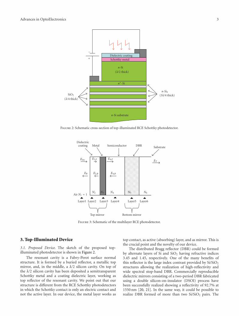
Figure 2: Schematic cross-section of top-illuminated RCE Schottky photodetector.
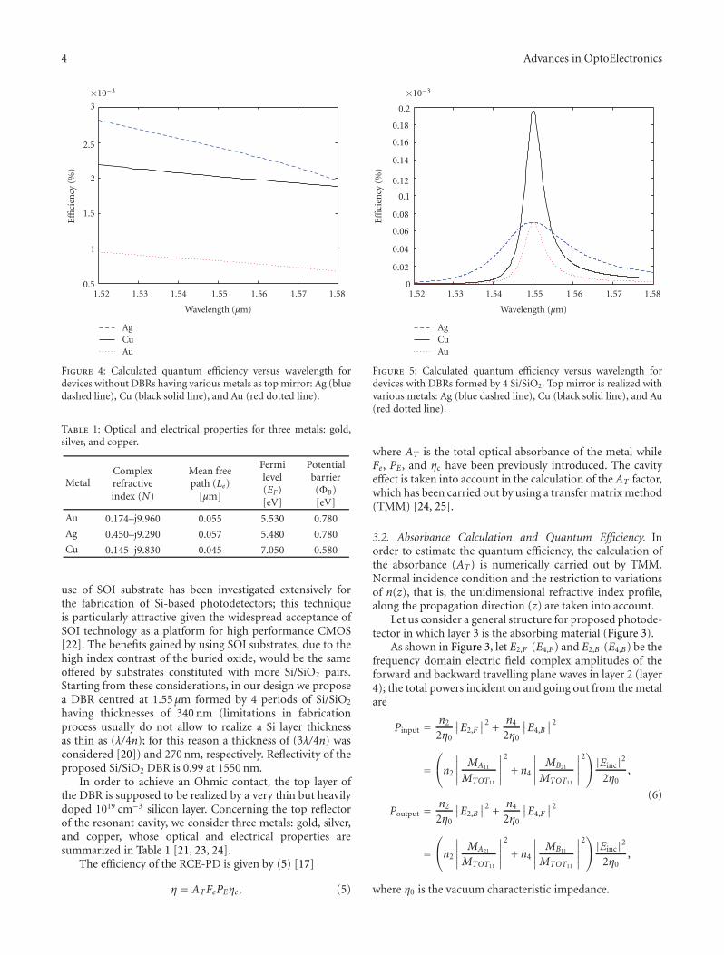
Top mirror Bottom mirror
Layer1 Layer2 Layer3 Layer4 Layer5 Layer6
Dielectriccoating Metal Semiconductor DBR Substrate
Einc E2,F E4,F ET
ER E2,B E4,B
Air N1 = 1N2 N3 N4 N5 N6
Figure 3: Schematic of the multilayer RCE photodetector.
3. Top-Illuminated Device
3.1. Proposed Device. The sketch of the proposed top-illuminated photodetector is shown in Figure 2.
The resonant cavity is a Fabry-Perot surface normalstructure. It is formed by a buried reflector, a metallic topmirror, and, in the middle, a λ/2 silicon cavity. On top ofthe λ/2 silicon cavity has been deposited a semitransparentSchottky metal and a coating dielectric layer, working astop reflector of the resonant cavity. We point out that ourstructure is different from the RCE Schottky photodetectorsin which the Schottky contact is only an electric contact andnot the active layer. In our device, the metal layer works as
top contact, as active (absorbing) layer, and as mirror. This isthe crucial point and the novelty of our device.
The distributed Bragg reflector (DBR) could be formedby alternate layers of Si and SiO2 having refractive indices3.45 and 1.45, respectively. One of the many benefits ofthis reflector is the large index contrast provided by Si/SiO2
structures allowing the realization of high-reflectivity andwide spectral stop-band DBR. Commercially reproducibledielectric mirrors consisting of a two-period DBR fabricatedusing a double silicon-on-insulator (DSOI) process havebeen successfully realized showing a reflectivity of 92.7% at1550 nm [20, 21]. In the same way, it could be possible torealize DBR formed of more than two Si/SiO2 pairs. The
4 Advances in OptoElectronics
0.5
1
1.5
2
2.5
3
×10−3
Effi
cien
cy(%
)
1.52 1.53 1.54 1.55 1.56 1.57 1.58
Wavelength (μm)
AgCuAu
Figure 4: Calculated quantum efficiency versus wavelength fordevices without DBRs having various metals as top mirror: Ag (bluedashed line), Cu (black solid line), and Au (red dotted line).
Table 1: Optical and electrical properties for three metals: gold,silver, and copper.
MetalComplexrefractiveindex (N)
Mean freepath (Le)
[μm]
Fermilevel(EF)[eV]
Potentialbarrier(ΦB)[eV]
Au 0.174–j9.960 0.055 5.530 0.780
Ag 0.450–j9.290 0.057 5.480 0.780
Cu 0.145–j9.830 0.045 7.050 0.580
use of SOI substrate has been investigated extensively forthe fabrication of Si-based photodetectors; this techniqueis particularly attractive given the widespread acceptance ofSOI technology as a platform for high performance CMOS[22]. The benefits gained by using SOI substrates, due to thehigh index contrast of the buried oxide, would be the sameoffered by substrates constituted with more Si/SiO2 pairs.Starting from these considerations, in our design we proposea DBR centred at 1.55 μm formed by 4 periods of Si/SiO2
having thicknesses of 340 nm (limitations in fabricationprocess usually do not allow to realize a Si layer thicknessas thin as (λ/4n); for this reason a thickness of (3λ/4n) wasconsidered [20]) and 270 nm, respectively. Reflectivity of theproposed Si/SiO2 DBR is 0.99 at 1550 nm.
In order to achieve an Ohmic contact, the top layer ofthe DBR is supposed to be realized by a very thin but heavilydoped 1019 cm−3 silicon layer. Concerning the top reflectorof the resonant cavity, we consider three metals: gold, silver,and copper, whose optical and electrical properties aresummarized in Table 1 [21, 23, 24].
The efficiency of the RCE-PD is given by (5) [17]
η = ATFePEηc, (5)
0
0.02
0.04
0.06
0.08
0.1
0.12
0.14
0.16
0.18
0.2
×10−3
Effi
cien
cy(%
)
1.52 1.53 1.54 1.55 1.56 1.57 1.58
Wavelength (μm)
AgCuAu
Figure 5: Calculated quantum efficiency versus wavelength fordevices with DBRs formed by 4 Si/SiO2. Top mirror is realized withvarious metals: Ag (blue dashed line), Cu (black solid line), and Au(red dotted line).
where AT is the total optical absorbance of the metal whileFe, PE, and ηc have been previously introduced. The cavityeffect is taken into account in the calculation of theAT factor,which has been carried out by using a transfer matrix method(TMM) [24, 25].
3.2. Absorbance Calculation and Quantum Efficiency. Inorder to estimate the quantum efficiency, the calculation ofthe absorbance (AT) is numerically carried out by TMM.Normal incidence condition and the restriction to variationsof n(z), that is, the unidimensional refractive index profile,along the propagation direction (z) are taken into account.
Let us consider a general structure for proposed photode-tector in which layer 3 is the absorbing material (Figure 3).
As shown in Figure 3, let E2,F (E4,F) and E2,B (E4,B) be thefrequency domain electric field complex amplitudes of theforward and backward travelling plane waves in layer 2 (layer4); the total powers incident on and going out from the metalare
Pinput =n2
2η0
∣∣E2,F∣∣2 +
n4
2η0
∣∣E4,B∣∣2
=⎛⎝n2
∣∣∣∣∣MA11
MTOT11
∣∣∣∣∣2
+ n4
∣∣∣∣∣MB21
MTOT11
∣∣∣∣∣2⎞⎠ |Einc|2
2η0,
Poutput = n2
2η0
∣∣E2,B∣∣2 +
n4
2η0
∣∣E4,F∣∣2
=⎛⎝n2
∣∣∣∣∣MA21
MTOT11
∣∣∣∣∣2
+ n4
∣∣∣∣∣MB11
MTOT11
∣∣∣∣∣2⎞⎠ |Einc|2
2η0,
(6)
where η0 is the vacuum characteristic impedance.
Advances in OptoElectronics 5
+
−
Al AlCu Schottky metal
p-Si
Dielectric bottom mirror
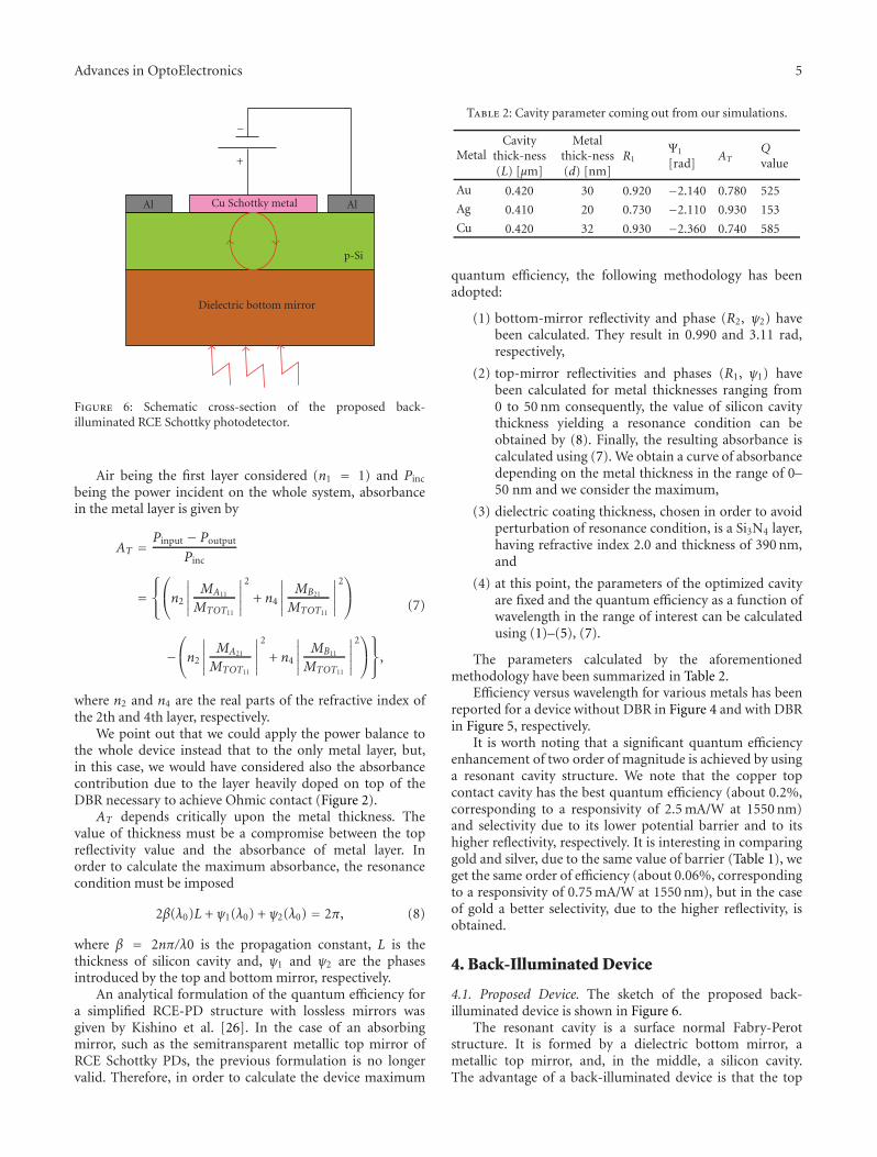
Figure 6: Schematic cross-section of the proposed back-illuminated RCE Schottky photodetector.
Air being the first layer considered (n1 = 1) and Pinc
being the power incident on the whole system, absorbancein the metal layer is given by
AT =Pinput − Poutput
Pinc
=⎧⎨⎩
⎛⎝n2
∣∣∣∣∣MA11
MTOT11
∣∣∣∣∣2
+ n4
∣∣∣∣∣MB21
MTOT11
∣∣∣∣∣2⎞⎠
−⎛⎝n2
∣∣∣∣∣MA21
MTOT11
∣∣∣∣∣2
+ n4
∣∣∣∣∣MB11
MTOT11
∣∣∣∣∣2⎞⎠⎫⎬⎭,
(7)
where n2 and n4 are the real parts of the refractive index ofthe 2th and 4th layer, respectively.
We point out that we could apply the power balance tothe whole device instead that to the only metal layer, but,in this case, we would have considered also the absorbancecontribution due to the layer heavily doped on top of theDBR necessary to achieve Ohmic contact (Figure 2).
AT depends critically upon the metal thickness. Thevalue of thickness must be a compromise between the topreflectivity value and the absorbance of metal layer. Inorder to calculate the maximum absorbance, the resonancecondition must be imposed
2β(λ0)L + ψ1(λ0) + ψ2(λ0) = 2π, (8)
where β = 2nπ/λ0 is the propagation constant, L is thethickness of silicon cavity and, ψ1 and ψ2 are the phasesintroduced by the top and bottom mirror, respectively.
An analytical formulation of the quantum efficiency fora simplified RCE-PD structure with lossless mirrors wasgiven by Kishino et al. [26]. In the case of an absorbingmirror, such as the semitransparent metallic top mirror ofRCE Schottky PDs, the previous formulation is no longervalid. Therefore, in order to calculate the device maximum
Table 2: Cavity parameter coming out from our simulations.
MetalCavity
thick-ness(L) [μm]
Metalthick-ness(d) [nm]
R1Ψ1
[rad]AT
Qvalue
Au 0.420 30 0.920 −2.140 0.780 525
Ag 0.410 20 0.730 −2.110 0.930 153
Cu 0.420 32 0.930 −2.360 0.740 585
quantum efficiency, the following methodology has beenadopted:
(1) bottom-mirror reflectivity and phase (R2, ψ2) havebeen calculated. They result in 0.990 and 3.11 rad,respectively,
(2) top-mirror reflectivities and phases (R1, ψ1) havebeen calculated for metal thicknesses ranging from0 to 50 nm consequently, the value of silicon cavitythickness yielding a resonance condition can beobtained by (8). Finally, the resulting absorbance iscalculated using (7). We obtain a curve of absorbancedepending on the metal thickness in the range of 0–50 nm and we consider the maximum,
(3) dielectric coating thickness, chosen in order to avoidperturbation of resonance condition, is a Si3N4 layer,having refractive index 2.0 and thickness of 390 nm,and
(4) at this point, the parameters of the optimized cavityare fixed and the quantum efficiency as a function ofwavelength in the range of interest can be calculatedusing (1)–(5), (7).
The parameters calculated by the aforementionedmethodology have been summarized in Table 2.
Efficiency versus wavelength for various metals has beenreported for a device without DBR in Figure 4 and with DBRin Figure 5, respectively.
It is worth noting that a significant quantum efficiencyenhancement of two order of magnitude is achieved by usinga resonant cavity structure. We note that the copper topcontact cavity has the best quantum efficiency (about 0.2%,corresponding to a responsivity of 2.5 mA/W at 1550 nm)and selectivity due to its lower potential barrier and to itshigher reflectivity, respectively. It is interesting in comparinggold and silver, due to the same value of barrier (Table 1), weget the same order of efficiency (about 0.06%, correspondingto a responsivity of 0.75 mA/W at 1550 nm), but in the caseof gold a better selectivity, due to the higher reflectivity, isobtained.
4. Back-Illuminated Device
4.1. Proposed Device. The sketch of the proposed back-illuminated device is shown in Figure 6.
The resonant cavity is a surface normal Fabry-Perotstructure. It is formed by a dielectric bottom mirror, ametallic top mirror, and, in the middle, a silicon cavity.The advantage of a back-illuminated device is that the top
6 Advances in OptoElectronics
2
4
6
8
10
12
14
16
18
20
Res
pon
sivi
ty(μ
A/W
)
1548 1549 1550 1551 1552 1553 1554 1555
Wavelength (nm)
RBM = 0.3RBM = 0.73RBM = 0.98
Figure 7: Responsivity versus Wavelength at bottom-mirror reflec-tivities (RBM) of 0.3 (blue solid line), 0.73 (red dotted line), and 0.98(black dashed line).
Cu Schottkycontact
Al nonrectifyingcontact
2 mm
Figure 8: Top view of the back-illuminated realized photodetector.
mirror can be realized very thick reducing the importanceof the roughness control during metal deposition process.The dielectric bottom reflector will be realized by alternatinglayers of amorphous hydrogenated silicon (a-Si:H) andsilicon nitride (Si3N4) having λ/4 thicknesses.
4.2. Responsivity Calculation. By (1)–(5) and (7), deviceshaving bottom-mirror reflectivities (RBM) of 0.3 (reflectivityof a silicon/air interface), 0.73, and 0.98 were numericallyinvestigated. All optical and electrical properties for siliconand copper used in our simulations are reported in Table 3[21, 23–27].
Table 3: Optical and electrical properties for silicon and copperused in our simulations.
Complexrefractiveindex at1550 nm
Thickness[μm]
Meanfree path(Le) [μm]
Fermilevel (EF)
[eV]
Potentialbarrier(ΦB)[eV]
Copper(Cu)
0.145-j9.830
0.20 0.045 7.050 0.720
Silicon 3.48 100 — — —
Table 4: Cavity parameters coming out from our simulations.
Peak responsivity[uA/W]
Cavity finesse
Cu/p-Si photodiodewith bottom reflectivityat 1550 nm of 0.30
3 4.7
Cu/p-Si photodiodewith bottom reflectivityat 1550 nm of 0.73
9.1 16.5
Cu/p-Si photodiodewith bottom reflectivityat 1550 nm of 0.98
19.9 89
In Figure 7, responsivity (linked to the efficiency by theformula: R = (λ[nm]/1242)η) versus wavelength at variousbottom-mirror reflectivities is reported.
The results coming out of our simulation are summa-rized in Table 4.
In all cases, the free spectral range is 3.3 nm. It is worthnoting that a responsivity enhancement is achieved by usingresonant cavity structure at higher finesse. The maximumresponsivity of 19.9 μA/W obtained in our simulations isabout two orders of magnitude lower compared with the top-illuminated structure numerically investigated above. This isexpected from the fact that in top illuminated structure thegoal was to optimize the device in order to get the highestefficiency while in this back-illuminated structure the layerthicknesses are chosen taking into account our capability torealize a preliminary device in order to make a comparisonbetween theoretical and experimental data.
4.3. Device Fabrication. In order to validate our numericalresults, we only fabricated back-illuminated structures in twovariants: one with high-reflectivity bottom mirror realizedwith 5 pairs of a-Si:H/Si3N4 and one with a low reflectivitybottom mirror realized with simple silicon/air interface. Bothstructures have been provided by Cu metal working as thetop mirror.
The samples were fabricated starting from a slightlydoped (1014 cm−3) p-type bi-polished 100-μm-thick siliconwafer.
The collecting ohmic contact was realized on the top ofthe samples. The collecting contact was made by a 200-nm-thick aluminum film, thermally evaporated at 3 · 10−6 mbarand 150◦C, and patterned by a lift-off process of photoresistShipley S1813 which, deposited by a spincoater at 4000 rpm,has a thickness of 1.4 μm. Then, an annealing at 475◦C in
Advances in OptoElectronics 7
Table 5: Value of thicknesses and refractive indices as calculated.
D [nm] n1550
a-Si:H 108 3.58
Si3N4 220 1.82
nitrogen for 30 min, in order to get a not-rectifying behavior,was carried out [28].
On the back of one device, a multilayer Bragg mirror wasfabricated by Plasma Enhanced Chemical Vapor Depositiontechnique (PECVD). The mirror is composed by a quarter-wave stack of a-Si:H and Si3N4 layers, having nominal refrac-tive index, at 1550 nm, of 3.52 and 1.82, respectively. Siliconnitride was deposited at pressure of 1.2 mbar, temperatureof 250◦C, at 30 W of RF power. In the deposition chamber,10 sccm of NH3, 88 sccm of SiH4 (5% in He), and 632 sccmof N2 were flowed. The deposition rate is 22.93 nm/min, andthe suitable Si3N4 thickness was obtained with a process timeof 9 min and 17 sec. The amorphous hydrogenated silicon,instead, was deposited at pressure of 0.8 mbar, temperatureof 250◦C, power of 2 W, and a SiH4 (5% in He) flow of600 sccm. The a-Si:H deposition rate is 3.15 nm/min, and thesuitable thickness was obtained with a process time of 34 minand 56 sec.
Finally, the Schottky contact was fabricated on topof both samples. Copper was thermally evaporated andpatterned by liftoff, so obtaining a metal thickness of 200 nm,thicker than optical field penetration depth. The collectingcontact and the Schottky contact are shaped by a ring and adisk having radius of about 2 mm, as shown in Figure 8.
4.4. Device Characterization
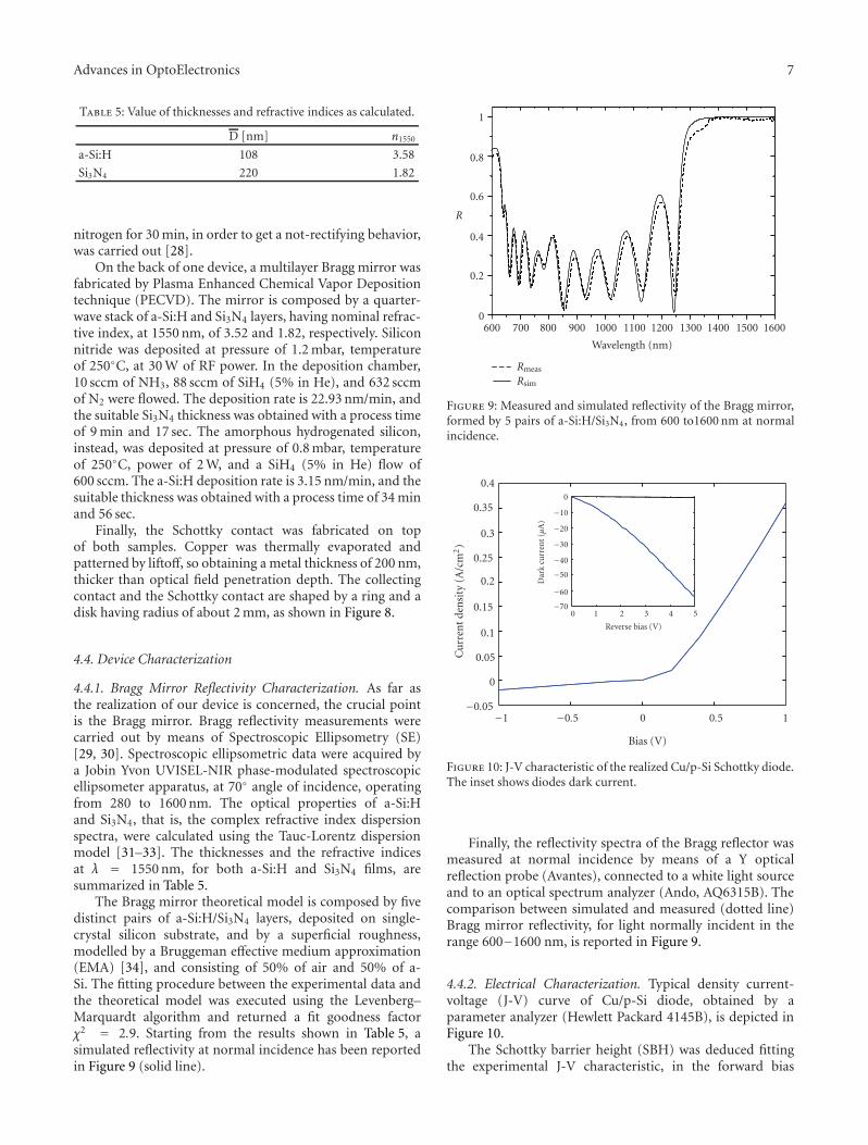
4.4.1. Bragg Mirror Reflectivity Characterization. As far asthe realization of our device is concerned, the crucial pointis the Bragg mirror. Bragg reflectivity measurements werecarried out by means of Spectroscopic Ellipsometry (SE)[29, 30]. Spectroscopic ellipsometric data were acquired bya Jobin Yvon UVISEL-NIR phase-modulated spectroscopicellipsometer apparatus, at 70◦ angle of incidence, operatingfrom 280 to 1600 nm. The optical properties of a-Si:Hand Si3N4, that is, the complex refractive index dispersionspectra, were calculated using the Tauc-Lorentz dispersionmodel [31–33]. The thicknesses and the refractive indicesat λ = 1550 nm, for both a-Si:H and Si3N4 films, aresummarized in Table 5.
The Bragg mirror theoretical model is composed by fivedistinct pairs of a-Si:H/Si3N4 layers, deposited on single-crystal silicon substrate, and by a superficial roughness,modelled by a Bruggeman effective medium approximation(EMA) [34], and consisting of 50% of air and 50% of a-Si. The fitting procedure between the experimental data andthe theoretical model was executed using the Levenberg–Marquardt algorithm and returned a fit goodness factorχ2 = 2.9. Starting from the results shown in Table 5, asimulated reflectivity at normal incidence has been reportedin Figure 9 (solid line).
0
0.2
0.4
0.6
0.8
1
R
600 700 800 900 1000 1100 1200 1300 1400 1500 1600
Wavelength (nm)
Rmeas
Rsim
Figure 9: Measured and simulated reflectivity of the Bragg mirror,formed by 5 pairs of a-Si:H/Si3N4, from 600 to1600 nm at normalincidence.
−0.05
0
0.05
0.1
0.15
0.2
0.25
0.3
0.35
0.4
Cu
rren
tde
nsi
ty(A
/cm
2)
−1 −0.5 0 0.5 1
Bias (V)
−70
−60
−50
−40
−30
−20
−10
0
Dar
kcu
rren
t(μ
A)
0 1 2 3 4 5
Reverse bias (V)
Figure 10: J-V characteristic of the realized Cu/p-Si Schottky diode.The inset shows diodes dark current.
Finally, the reflectivity spectra of the Bragg reflector wasmeasured at normal incidence by means of a Y opticalreflection probe (Avantes), connected to a white light sourceand to an optical spectrum analyzer (Ando, AQ6315B). Thecomparison between simulated and measured (dotted line)Bragg mirror reflectivity, for light normally incident in therange 600−1600 nm, is reported in Figure 9.
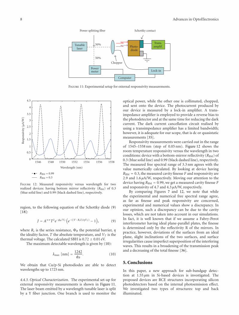
4.4.2. Electrical Characterization. Typical density current-voltage (J-V) curve of Cu/p-Si diode, obtained by aparameter analyzer (Hewlett Packard 4145B), is depicted inFigure 10.
The Schottky barrier height (SBH) was deduced fittingthe experimental J-V characteristic, in the forward bias
8 Advances in OptoElectronics
Tunablelaser
Powermeter
Chopper
Computer
Lock-in
Trans.amplif.Photo-
diode
Power splitting fiber Schottky contact
50%
50%
Figure 11: Experimental setup for external responsivity measurements.
0
0.5
1
1.5
2
2.5
3
3.5
4
4.5
Res
pon
sivi
ty(μ
A/W
)
1546 1548 1550 1552 1554 1556 1558
Wavelength (nm)
RBM = 0.99RBM = 0.3
Figure 12: Measured responsivity versus wavelength for tworealized devices: having bottom mirror reflectivity (RBM) of 0.3(blue solid line) and 0.99 (black dashed line), respectively.
region, to the following equation of the Schottky diode (9)[18]:
J = A∗∗T2e−φB/VT(e−((V−RsI)/ηVT ) − 1
), (9)
where Rs is the series resistance, ΦB the potential barrier, ηthe ideality factor, T the absolute temperature, and VT is thethermal voltage. The calculated SBH is 0.72 ± 0.01 eV.
The maximum detectable wavelength is given by (10):
λmax [nm] = 1242φB
. (10)
We obtain that Cu/p-Si photodiodes are able to detectwavelengths up to 1725 nm.
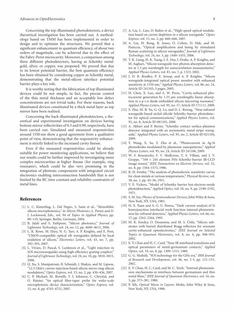
4.4.3. Optical Characterization. The experimental set-up forexternal responsivity measurements is shown in Figure 11.The laser beam emitted by a wavelength tunable laser is splitby a Y fiber junction. One branch is used to monitor the
optical power, while the other one is collimated, chopped,and sent onto the device. The photocurrent produced byour device is measured by a lock-in amplifier. A trans-impedance amplifier is employed to provide a reverse bias tothe photodetector and at the same time for reducing the darkcurrent. The dark current cancellation circuit realised byusing a transimpedance amplifier has a limited bandwidth;however, it is adequate for our scope, that is dc or quasistaticmeasurements [35].
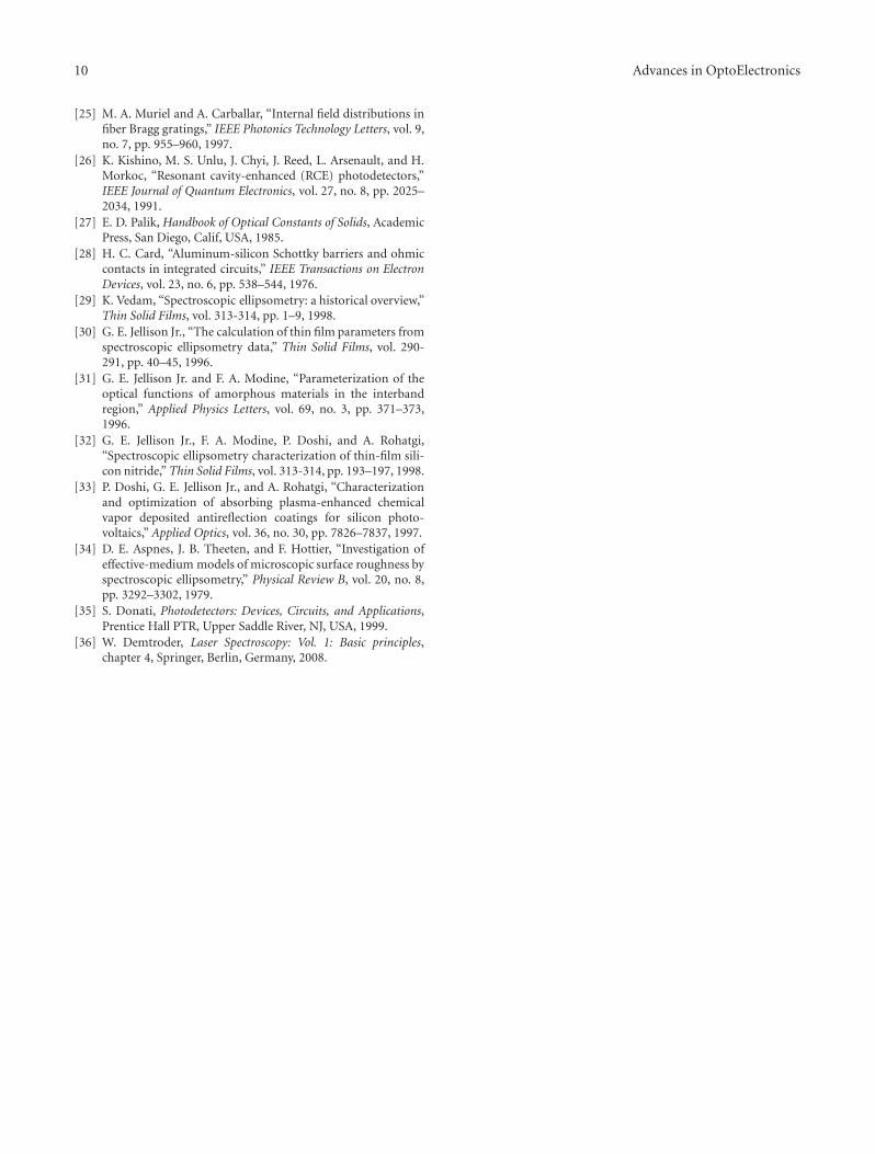
Responsivity measurements were carried out in the rangeof 1545–1558 nm (step of 0.05 nm). Figure 12 shows theroom temperature responsivity versus the wavelength in twoconditions: device with a bottom-mirror reflectivity (RBM) of0.3 (blue solid line) and 0.99 (black dashed line), respectively.The measured free spectral range of 3.3 nm agrees with thevalue numerically calculated. By looking at device havingRBM = 0.3, the measured cavity finesse F and responsivity are2.9 and 1.6 μA/W, respectively. Moving our attention to thedevice having RBM = 0.99, we get a measured cavity finesse Fand responsivity of 4.7 and 4.3 μA/W, respectively.
By comparing Figures 7 and 12, we note that whilethe experimental and numerical free spectral range agree,as far as finesse and peak responsivity are concerned,experimental and numerical values show a discrepancy. Inour opinion, such a discrepancy can be due to the cavitylosses, which are not taken into account in our simulations.In fact, it is well known that if we assume a Fabry-Perotinterferometer having ideal plane-parallel plates, the finesseis determined only by the reflectivity R of the mirrors. Inpractice, however, deviations of the surfaces from an idealplane, slight inclinations of the two surfaces, and surfaceirregularities cause imperfect superposition of the interferingwaves. This results in a broadening of the transmission peakand a decreasing of the total finesse [36].
5. Conclusions
In this paper, a new approach for sub-bandgap detec-tion at 1.55 μm in Si-based devices is investigated. Theproposed devices are RCE structures incorporating siliconphotodetectors based on the internal photoemission effect.We investigated two types of structures: top and backilluminated.
Advances in OptoElectronics 9
Concerning the top-illuminated photodetectors, a devicetheoretical investigation has been carried out. A method-ology based on TMM has been implemented in order todesign and to optimize the structures. We proved that asignificant enhancement in quantum efficiency, of about twoorders of magnitude, can be achieved due to the effect ofthe Fabry-Perot microcavity. Moreover, a comparison amongthree different photodetectors, having as Schottky metal:gold, silver, or copper, was proposed. We proved that dueto its lowest potential barrier, the best quantum efficiencyhas been obtained by considering copper as Schottky metal,demonstrating that the metal-silicon interface potentialbarrier plays a key role.
It is worthy noting that the fabrication of top illuminateddevices could be not simple, in fact, the precise controlof the thin metal thickness and an acceptably low defectconcentrations are not trivial tasks. For these reasons, backilluminated devices constituted by a thick metal layer as topmirror have been realized.
Concerning the back-illuminated photodetectors, a the-oretical and experimental investigation on devices havingbottom mirror reflectivities of 0.3 and 0.99, respectively, havebeen carried out. Simulated and measured responsivitiesaround 1550 nm show a good agreement from a qualitativepoint of view, demonstrating that the responsivity enhance-ment is strictly linked to the increased cavity finesse.
Even if the measured responsivities could be alreadysuitable for power monitoring applications, we believe thatour results could be further improved by investigating morecomplex microcavities at higher finesse (for example, ringresonator), which could be also very promising in theintegration of photonic components with integrated circuitelectronics enabling interconnection bandwidth that is notlimited by the RC time constant and reliability constraints ofmetal lines.
References
[1] L. C. Kimerling, L. Dal Negro, S. Saini et al., “Monolithicsilicon microphotonics,” in Silicon Photonics, L. Pavesi and D.J. Lockwood, Eds., vol. 94 of Topics in Applied Physics, pp.89–119, Springer, Berlin, Germany, 2004.
[2] B. Jalali and S. Fathpour, “Silicon photonics,” Journal ofLightwave Technology, vol. 24, no. 12, pp. 4600–4615, 2006.
[3] L. K. Rowe, M. Elsey, N. G. Tarr, A. P. Knights, and E. Post,“CMOS-compatible optical rib waveguides defined by localoxidation of silicon,” Electronics Letters, vol. 43, no. 7, pp.392–393, 2007.
[4] L. Vivien, D. Pascal, S. Lardenois et al., “Light injection inSOI microwaveguides using high-efficiency grating couplers,”Journal of Lightwave Technology, vol. 24, no. 10, pp. 3810–3815,2006.
[5] Q. Xu, S. Manipatruni, B. Schmidt, J. Shakya, and M. Lipson,“12.5 Gbit/s carrier-injection-based silicon micro-ring siliconmodulators,” Optics Express, vol. 15, no. 2, pp. 430–436, 2007.
[6] C. P. Michael, M. Borselli, T. J. Johnson, C. Chrystal, andO. Painter, “An optical fiber-taper probe for wafer-scalemicrophotonic device characterization,” Optics Express, vol.15, no. 8, pp. 4745–4752, 2007.
[7] A. Liu, L. Liao, D. Rubin et al., “High-speed optical modula-tion based on carrier depletion in a silicon waveguide,” OpticsExpress, vol. 15, no. 2, pp. 660–668, 2007.
[8] A. Liu, H. Rong, R. Jones, O. Cohen, D. Hak, and M.Paniccia, “Optical amplification and lasing by stimulatedRaman scattering in silicon waveguides,” Journal of LightwaveTechnology, vol. 24, no. 3, pp. 1440–1455, 2006.
[9] T. K. Liang, H. K. Tsang, I. E. Day, J. Drake, A. P. Knights, andM. Asghari, “Silicon waveguide two-photon absorption detec-tor at 1.5 μm wavelength for autocorrelation measurements,”Applied Physics Letters, vol. 81, no. 7, p. 1323, 2002.
[10] J. D. B. Bradley, P. E. Jessop, and A. P. Knights, “Siliconwaveguide-integrated optical power monitor with enhancedsensitivity at 1550 nm,” Applied Physics Letters, vol. 86, no. 24,Article ID 241103, 3 pages, 2005.
[11] H. Chen, X. Luo, and A. W. Poon, “Cavity-enhanced pho-tocurrent generation by 1.55 μm wavelengths linear absorp-tion in a p-i-n diode embedded silicon microring resonator,”Applied Physics Letters, vol. 95, no. 17, Article ID 171111, 2009.
[12] S. Zhu, M. B. Yu, G. Q. Lo, and D. L. Kwong, “Near-infraredwaveguide-based nickel silicide Schottky-barrier photodetec-tor for optical communications,” Applied Physics Letters, vol.92, no. 8, Article ID 081103, 2008.
[13] A. Akbari and P. Berini, “Schottky contact surface-plasmondetector integrated with an asymmetric metal stripe waveg-uide,” Applied Physics Letters, vol. 95, no. 2, Article ID 021104,2009.
[14] Y. Wang, X. Su, Y. Zhu et al., “Photocurrent in Ag-Siphotodiodes modulated by plasmonic nanopatterns,” AppliedPhysics Letters, vol. 95, no. 24, Article ID 241106, 2009.
[15] W. F. Kosonocky, F. V. Shallcross, T. S. Villani, and J. V.Groppe, “160 × 244 element PtSi Schottky-barrier IR-CCDimage sensor,” IEEE Transactions on Electron Devices, vol. 32,no. 8, pp. 1564–1573, 1986.
[16] R. H. Fowler, “The analysis of photoelectric sensitivity curvesfor clean metals at various temperatures,” Physical Review, vol.38, no. 1, pp. 45–56, 1931.
[17] V. E. Vickers, “Model of Schottky barrier hot-electron-modephotodetection,” Applied Optics, vol. 10, no. 9, pp. 2190–2192,1971.
[18] S. M. Sze, Physics of Semiconductor Devices, John Wiley & Sons,New York, NY, USA, 1981.
[19] H. X. Yuan and A. G. U. Perera, “Dark current analysis of Sihomojunction interfacial work function internal photoemis-sion far-infrared detectors,” Applied Physics Letters, vol. 66, no.17, pp. 2262–2264, 1995.
[20] M. K. Emsley, O. Dosunmu, and M. S. Unlu, “Silicon sub-strates with buried distributed Bragg reflectors for resonantcavity-enhanced optoelectronics,” IEEE Journal on SelectedTopics in Quantum Electronics, vol. 8, no. 4, pp. 948–955,2002.
[21] E. Y. Chan and H. C. Card, “Near IR interband transitions andoptical parameters of metal-germanium contacts,” AppliedOptics, vol. 19, no. 8, pp. 1309–1315, 1980.
[22] G. G. Shahidi, “SOI technology for the GHz era,” IBM Journalof Research and Development, vol. 46, no. 2-3, pp. 121–131,2002.
[23] E. Y. Chan, H. C. Card, and M. C. Teich, “Internal photoemis-sion mechanisms at interfaces between germanium and thinmetal films,” IEEE Journal of Quantum Electronics, vol. 16, no.3, pp. 373–381, 1980.
[24] P. Yeh, Optical Waves in Layerer Media, John Wiley & Sons,New York, NY, USA, 1988.
10 Advances in OptoElectronics
[25] M. A. Muriel and A. Carballar, “Internal field distributions infiber Bragg gratings,” IEEE Photonics Technology Letters, vol. 9,no. 7, pp. 955–960, 1997.
[26] K. Kishino, M. S. Unlu, J. Chyi, J. Reed, L. Arsenault, and H.Morkoc, “Resonant cavity-enhanced (RCE) photodetectors,”IEEE Journal of Quantum Electronics, vol. 27, no. 8, pp. 2025–2034, 1991.
[27] E. D. Palik, Handbook of Optical Constants of Solids, AcademicPress, San Diego, Calif, USA, 1985.
[28] H. C. Card, “Aluminum-silicon Schottky barriers and ohmiccontacts in integrated circuits,” IEEE Transactions on ElectronDevices, vol. 23, no. 6, pp. 538–544, 1976.
[29] K. Vedam, “Spectroscopic ellipsometry: a historical overview,”Thin Solid Films, vol. 313-314, pp. 1–9, 1998.
[30] G. E. Jellison Jr., “The calculation of thin film parameters fromspectroscopic ellipsometry data,” Thin Solid Films, vol. 290-291, pp. 40–45, 1996.
[31] G. E. Jellison Jr. and F. A. Modine, “Parameterization of theoptical functions of amorphous materials in the interbandregion,” Applied Physics Letters, vol. 69, no. 3, pp. 371–373,1996.
[32] G. E. Jellison Jr., F. A. Modine, P. Doshi, and A. Rohatgi,“Spectroscopic ellipsometry characterization of thin-film sili-con nitride,” Thin Solid Films, vol. 313-314, pp. 193–197, 1998.
[33] P. Doshi, G. E. Jellison Jr., and A. Rohatgi, “Characterizationand optimization of absorbing plasma-enhanced chemicalvapor deposited antireflection coatings for silicon photo-voltaics,” Applied Optics, vol. 36, no. 30, pp. 7826–7837, 1997.
[34] D. E. Aspnes, J. B. Theeten, and F. Hottier, “Investigation ofeffective-medium models of microscopic surface roughness byspectroscopic ellipsometry,” Physical Review B, vol. 20, no. 8,pp. 3292–3302, 1979.
[35] S. Donati, Photodetectors: Devices, Circuits, and Applications,Prentice Hall PTR, Upper Saddle River, NJ, USA, 1999.
[36] W. Demtroder, Laser Spectroscopy: Vol. 1: Basic principles,chapter 4, Springer, Berlin, Germany, 2008.

International Journal of
AerospaceEngineeringHindawi Publishing Corporationhttp://www.hindawi.com Volume 2010
RoboticsJournal of
Hindawi Publishing Corporationhttp://www.hindawi.com Volume 2014
Hindawi Publishing Corporationhttp://www.hindawi.com Volume 2014
Active and Passive Electronic Components
Control Scienceand Engineering
Journal of
Hindawi Publishing Corporationhttp://www.hindawi.com Volume 2014
International Journal of
RotatingMachinery
Hindawi Publishing Corporationhttp://www.hindawi.com Volume 2014
Hindawi Publishing Corporation http://www.hindawi.com
Journal ofEngineeringVolume 2014
Submit your manuscripts athttp://www.hindawi.com
VLSI Design
Hindawi Publishing Corporationhttp://www.hindawi.com Volume 2014
Hindawi Publishing Corporationhttp://www.hindawi.com Volume 2014
Shock and Vibration
Hindawi Publishing Corporationhttp://www.hindawi.com Volume 2014
Civil EngineeringAdvances in
Acoustics and VibrationAdvances in
Hindawi Publishing Corporationhttp://www.hindawi.com Volume 2014
Hindawi Publishing Corporationhttp://www.hindawi.com Volume 2014
Electrical and Computer Engineering
Journal of
Advances inOptoElectronics
Hindawi Publishing Corporation http://www.hindawi.com
Volume 2014
The Scientific World JournalHindawi Publishing Corporation http://www.hindawi.com Volume 2014
SensorsJournal of
Hindawi Publishing Corporationhttp://www.hindawi.com Volume 2014
Modelling & Simulation in EngineeringHindawi Publishing Corporation http://www.hindawi.com Volume 2014
Hindawi Publishing Corporationhttp://www.hindawi.com Volume 2014
Chemical EngineeringInternational Journal of Antennas and
Propagation
International Journal of
Hindawi Publishing Corporationhttp://www.hindawi.com Volume 2014
Hindawi Publishing Corporationhttp://www.hindawi.com Volume 2014
Navigation and Observation
International Journal of
Hindawi Publishing Corporationhttp://www.hindawi.com Volume 2014
DistributedSensor Networks
International Journal of