Remotely Up-Converted 20-Gbit/s Error-Free Wireless On–Off-Keying Data Transmission at W-Band...
12
Remotely Up-Converted 20-Gbit /s Error-Free Wireless On– Off-Keying Data Transmission at W-Band Using an Ultra-Wideband Photonic Transmitter-Mixer Volume 3, Number 2, April 2011 F.-M. Kuo C.-B. Huang J.-W. Shi Nan-Wei Chen H.-P. Chuang John E. Bowers Ci-Ling Pan DOI: 10.1109/JPHOT.2011.2126567 1943-0655/$26.00 ©2011 IEEE
Transcript of Remotely Up-Converted 20-Gbit/s Error-Free Wireless On–Off-Keying Data Transmission at W-Band...

Remotely Up-Converted 20-Gbit /s Error-Free Wireless On–Off-Keying Data Transmission at W-Band Using an Ultra-Wideband Photonic Transmitter-MixerVolume 3, Number 2, April 2011
F.-M. KuoC.-B. HuangJ.-W. ShiNan-Wei ChenH.-P. ChuangJohn E. BowersCi-Ling Pan
DOI: 10.1109/JPHOT.2011.21265671943-0655/$26.00 ©2011 IEEE
Remotely Up-Converted 20-Gbit/sError-Free Wireless On–Off-Keying Data
Transmission at W-Band Using anUltra-Wideband Photonic Transmitter-Mixer
F.-M. Kuo,1 C.-B. Huang,2 J.-W. Shi,1;3 Nan-Wei Chen,4 H.-P. Chuang,2John E. Bowers,3 and Ci-Ling Pan2
1Department of Electrical Engineering, National Central University, Taoyuan 320, Taiwan2Institute of Photonics Technologies, National Tsing-Hua Universit, Hsinchu 300, Taiwan
3Electrical and Computer Engineering Department, University of California, Santa Barbara,CA 93106 USA
4Department of Communications Engineering, Yuan Ze University, Taoyuan 320, Taiwan
DOI: 10.1109/JPHOT.2011.21265671943-0655/$26.00 �2011 IEEE
Manuscript received January 27, 2011; revised March 4, 2011; accepted March 5, 2011. Date ofpublication March 10, 2011; date of current version March 22, 2011. This work was supported bythe Ministry of Economic Affairs of Taiwan under Grant 98-EC-17-A-07-S1-001 and the NationalScience Council of Taiwan under Contract NSC-98-2221-E-008-009-MY3, Contract NSC-97-2112-M-007-025-MY3, and Contract NSC-98-2221-E-007-025-MY3. Corresponding author: J.-W. Shi (e-mail:[email protected]).
Abstract: We demonstrate a remotely up-converted and distributed 20-Gbit/s wirelesson–off-keying (OOK) data transmission link at the W-band that uses a near-ballistic uni-traveling-carrier photodiode (NBUTC-PD)-based photonic transmitter-mixer. This deviceconsists of an active NBUTC-PD integrated with a planar passive circuit for feeding theintermediate-frequency (IF) modulation input and extracting the up-converted optical-to-electrical (O–E) output signals. An equivalent-circuit model is developed, which allows forthe O–E and IF responses to be independently optimized. Accordingly, we can achieve bothan ultra-wide O–E bandwidth (67–118 GHz) and IF modulation bandwidth (9 15 GHz) with avery-low coupling loss (G 2 dB) from the NBUTC-PD to the WR-10 waveguide. We adopted aremotely distributed 1-ps optical pulse train source with a repetition rate at 93 GHz to serveas a high-performance photonic carrier, which is generated by a spectral line-by-line shaperutilizing the repetition-rate multiplication (RRM) technique. In contrast to lossy amplitudefiltering, our RRM is based on applying periodic loss-less spectral phase filtering onto the31-GHz comb lines. In comparison with the conventional 93-GHz sinusoidal carrier, thephotogenerated millimeter-wave (MMW) power of this kind of carrier is 4 dB higher than thatof PD under the same output photocurrent. In contrast to the traditional mode-locked laser,the fiber dispersion can be totally precompensated without additional dispersion compen-sation components. By use of such device and optical MMW source, we successfullydemonstrate remotely distributed and up-converted 20-Gbit/s error-free OOK wireless datatransmission link over a 25-km standard single-mode fiber.
Index Terms: Microwave photonics, photodetectors.
1. IntroductionWith the development of numerous kinds of multimedia services such as 3-D face-to-face commu-nication [1] and High-Definition Multimedia Interface (HDMI) 1.4 [2], the market demand for datacapacity on the scale of tens of gigabits per second has grown rapidly [3]–[5]. Radio-over-Fiber
Vol. 3, No. 2, April 2011 Page 209
IEEE Photonics Journal Wireless OOK Data Transmission at W-Band

(RoF) communication systems are considered to be one of the most suitable candidates to meetthis demand and to develop the desired ultra-broadband wireless access network [4]–[6]. However,it is still a challenge to acquire sufficient bandwidth for data transmission of tens of gigabits persecond over the last mile of such a system. One possible solution to this problem is to enlarge thespectral efficiency of the wireless link to transmit more data over the same bandwidth [4]. However,such a solution calls for a much higher signal-to-noise ratio (SNR) and requires a complex receiverto perform the demodulation/equalization process. Another possible solution is to straightforwardlyincrease the carrier frequency [5], but this requires photonic transmitters (PTs) with more optical-to-electrical (O–E) bandwidth in order to achieve a higher transmission data rate under the simpleon–off-keying (OOK) format. Using such an approach, a research group at Nippon Telegraph andTelephone (NTT) has demonstrated 14-Gbit/s error-free line-of-sight OOK wireless linking at the300-GHz band simply by using the uni-traveling-carrier photodiode (UTC-PD)-based PTs [5].However, fiber chromatic dispersion becomes more serious during long-haul distribution when boththe millimeter-wave (MMW) carrier frequency and data rate increase as is the case under theconventional RoF scheme [7]. Such a problem leads to serious signal fading and time-shiftingeffects, and thus limits the maximum fiber transmission distance of RoF systems. Furthermore, inorder to transmit multichannel data signals, the conventional RoF system requires more photonicMMW carrier signals at different optical wavelengths. This issue means a considerable occupation ofthe optical bandwidth when both the MMW carrier frequency and data rate increase. However, thecombination of remote signal up-conversion techniques with a nonlinear photodetection schemeprovides a promising solution for the aforementioned dispersion problem [7]. The photonic carrier(with fixed optical wavelengths) can thus be shared between different baseband channels in order tosave the required optical bandwidth. Ten gigabit-per-second signal generation [8] and 1.25-Gb/swireless data transmission [9] have been realized through the use of a nonlinear photodetectionscheme (bias modulation) with the UTC-PD. Furthermore, by use of the traveling-wave UTC-PD-based optoelectronic mixer, the nonlinear down-conversion experiment at 100 GHz radio frequency(RF), has been successfully achieved [10]. Nevertheless, it seems that the intermediate-frequency(IF) modulation bandwidth (�7 GHz) of the UTC-PD is limited by its switching speed [8]. This isdetermined by the required time constant from forward to reverse bias operations [8], which isnecessary for enhancing the nonlinearity and extinction ratio of the device during bias modulation.This problem can be overcome with our demonstrated near-ballistic uni-traveling-carrier photodiode(NBUTC-PD) high-performance optoelectronic mixer [11]. The flip-chip bonding packaged NBUTC-PD exhibits extremely high saturation current-bandwidth product (SCBP) performance (37 mA,110 GHz, 4070 mA-GHz) [12], [13], ultra-wide (9 10 GHz) IF modulation bandwidth (IMB) [11] andhigh (9 33 dB) extinction ratio during IF modulation [14]. The successful accomplishment of remotelyup-converted 12.5-Gbit/s OOK wireless data transmission at the W-band using the NBUTC-PD-based photonic transmitter-mixer (PTM) has been described in our previous work [14]. However, thedemonstrated maximum data rate is limited by the IMB, which is around 5 GHz. In this current study,we develop an equivalent-circuit model with a cascade topology to effectively and precisely design anovel PTM module [15], [16]. With this design, we simultaneously achieve an ultra-broadband O–Ebandwidth (67–118 GHz, fractional bandwidth 9 55.2%), ultra-wide IMB (9 15 GHz), and low (�2 dB)coupling loss from the NBUTC-PD to the WR-10 waveguide output.
In order to further realize the goal of high-performance data transmission, we also develop aremotely distributed 1-ps optical pulse trains with a repetition rate of 93 GHz to act as synchronizedhigh-performance photonic carrier for wireless data transmission [17]. In this paper, the 93-GHzoptical pulse trains are generated through repetition-rate multiplication (RRM) of an initially 31-GHzoptical pulse train via a spectral line-by-line shaper. RRM using both amplitude and phase filtering areperformed and the results are compared. Further information regarding RRM is provided in Section 3.The photogenerated (at a frequency of 93 GHz) MMW power of this carrier is 4 dB higher than that ofPD under the conventional 93-GHz sinusoidal carrier excitation with the same output photocurrent.Such a large improvement means that we may be able to reduce the optical power budget for datatransmission while resulting in better PTM reliability with the desired MMW output power.
IEEE Photonics Journal Wireless OOK Data Transmission at W-Band
Vol. 3, No. 2, April 2011 Page 210

In the work using mode-locked lasers for remote MMW power enhancement, dispersioncompensation must be carefully managed for the delivery of sub-picosecond optical pulses [18]. Asa direct comparison, here, we demonstrate that using our photonic MMW source, chromaticdispersion for a long fiber transmission distance of the sub-picosecond optical pulses can becompletely precompensated, without the need for additional dispersion compensation components[17]. In our experimental setup, the entire wireless link (after the up/down-conversion process andwith a pair of horn antennas) provides a 15-GHz channel bandwidth at the baseband for transmittingan ultra-broadband data signal. The high sensitivity (9 3 kV/W) of the detector and the high-powerperformance of the NBUTC-PD eliminates the need for W-band MMW amplifiers at both thetransmitting and receiving ends of our demonstrated link. Consequently, a remotely distributed andup-converted 20-Gbit/s error-free OOK wireless data transmission link over a 25-km standardsingle-mode fiber (SSMF) has been demonstrated successfully.
2. Device Structure and FabricationFig. 1 shows the top-view of the demonstrated novel NBUTC-PD-based PTM. As can be seen, it ismainly composed of a flip-chip bonded NBUTC-PD with a 100-�m2 active area, a bandpass filter(BPF), a band-stop filter (BSF), and a dipole-based feeding antenna (FA). The simulated frequencyresponses of the scattering (S) parameters of these three major passive components (BPF, BSF,and FA) are given in the insets to Fig. 1. As compared with the device described in our previouswork [14], the NBUTC-PD active device has a smaller active area (100-�m2 versus 144-�m2),which corresponds to a better speed performance (3-dB O–E bandwidth 9 200 GHz under a 25 �load) [12] which is important for achieving an ultra-wideband PTM. A slot-line (SL) structure on a150-�m thick aluminum nitride (AlN) substrate is employed for the passive circuits due to its goodthermal conductivity and reduced substrate mode [15]. As can be seen in the inset to Fig. 1, the FAshows a low coupling loss for feeding the MMW power into the WR-10 waveguide in the full W-band[15], [16]. For details about this component, see our previous work [15], [16]. In order tosimultaneously realize a fully integrated PTM module with an ultra-broadband O–E bandwidth, ultra-wide IMB, and low coupling loss from the NBUTC-PD to the WR-10 waveguide output, withoutaccuracy loss, we exploit a relatively efficient cascaded equivalent-circuit model rather thandemand the time-consuming full-wave analysis for chip characterization [15], [16]. Technically, thebuilding-block diagram of the entire system is provided in Fig. 2. It is shown that the accurate O–Ebandwidth and IMB are obtained with the inclusion of the undesired parasitic effects, especially from
Fig. 1. Top-view of the novel NBUTC-PD-based PTM. The insets give the simulated frequencyresponses of the scattering (S) parameters of the bandpass filter (BPF), band-stop filter (BSF), anddipole-based feeding antenna (FA).
IEEE Photonics Journal Wireless OOK Data Transmission at W-Band
Vol. 3, No. 2, April 2011 Page 211

the high dielectric constant InP substrate of the NBUTC-PD, as well as flip-chip bonding pillars forheat sinking [15], [16], in the proposed circuit model. In Fig. 2, the function of the passive circuitblocks, i.e., W-band BSF and BPF, is described as follows. In Fig. 2, the IF signal passing through aW-band BSF, which is also termed as the RF choke, is pumped into the NBUTC-PD for the opticalMMW source modulation. The modulated W-band source passing through a W-band BPF is thenforwarded to the waveguide feed of the horn antenna. Here, the BPF employed herein is forisolation enhancement between the IF port and the waveguide feed structure. In our previous work[15], the partially reflected W-band source from the feed is filtered out by the RF choke regarding theinput signal integrity. However, the IF signal is not completely delivered to the PD for biasmodulation since a fractional amount of the power leaks to the waveguide feed. With the BPF, the IFpower leakage is alleviated. In other words, the isolation between the IF port and the waveguidefeed is further enhanced, which leads to a significant improvement on the video bandwidth of thetransmitter. Based on the circuit design point of view, the good isolation at both W- and IF bandsrepresents a successful broadband impedance matching. Indeed, as can be seen in Fig. 1, theW-band BSF shows a high reflection (isolation, around 0 dB of S11 at the 75–110 GHz frequency) atthe W-band and reasonable transmission loss (S21 less than �3 dB) at the IF band (DC to 15 GHz).On the other hand, the BPF shows reasonable transmission loss ðS21 G�3 dBÞ at the W-band anda high rejection at the IF band (S21 less than �10 dB). Hence, this BPF–BSF pair can thus not onlyseparate the RF and IF signals into different flow paths but can also avoid leakage of the injected IFsignal and up-converted RF signal to the respective FA and IF input ports of the device. Thanks tothis separation, the impedance matching at the O–E and IF bands can be optimized independentlyand ultra-wide O–E and IF responses can thus be achieved.
3. Measurement ResultsFig. 3(a) and (b) illustrate the measurement setup of our NBUTC-PD chip, serving as a PTM moduleand a flip-chip bonding PD for high-power generation, respectively. In Fig. 3(a) and (b), bothNBUTC-PD chips have the same active area of 100 �m2. As can be seen in Fig. 3(a), the front-endof the PTM module is inserted into the WR-10 rectangular waveguide for excitation of itsfundamental propagation mode. At the same time, the electrical IF and optical local-oscillator (LO)signals are also fed into the PTM module through a microwave probe and lensed fiber, respectively.Note that the full PTM module is suspended in free space to suppress the undesired substratemode and obtain a low coupling loss [15], [16]. As can be seen in Fig. 3(b), for the case of high-power PD application, the full chip is directly mounted onto the metal chunk for good heat-sinking. Amicrowave probe is employed in (a) and (b) to feed the IF signal and extract the photogeneratedMMW power from the PD, respectively. When we measure the O–E responses of our PTM module,
Fig. 2. Schematic system building-block diagram.
IEEE Photonics Journal Wireless OOK Data Transmission at W-Band
Vol. 3, No. 2, April 2011 Page 212

the IF input port only provides a fixed DC bias voltage of �3 V, while the optical LO frequency isswept from 60 to 130 GHz.
Fig. 4(a) shows plots of the measured and simulated O–E responses of our PTM module, theO–E responses of the flip-chip bonded NBUTC-PD chip under a 50-� load [as shown in Fig. 3(b)],and the coupling loss of the planar dipole-based radiator to the WR-10 waveguide. Here, the 0 dBreference point of all frequency responses shown is defined as the output power from an idealphotodiode (i.e., infinite bandwidth) with a 50-� load, under an ideal sinusoidal optical sourceexcitation (100% modulation depth), and with the same output photocurrent (4 mA) as that of thePTM and PD. The frequency response of the coupling loss, which is defined as the MMW loss fromour planar dipole-based FA to WR-10 waveguide, can be extracted by subtracting the measuredO–E response for the full PTM module from the measured O–E response for the PD chip. As can beseen, ultra-wide 3-dB bandwidths (�67–118 GHz, �53 GHz) can be achieved for both the couplingloss and O–E response with small loss (G 2 dB) with our design. A smaller coupling loss can beexpected by further increasing the effective input impedance of our FA to over the 50-� loadresistance of the NBUTC-PD chip. Our demonstrated device exhibits a much higher fractionalbandwidth (9 55.2%, versus 24.2%) for the O–E response than that of the taper-slot antenna orpatch antenna coupled UTC-PD PT [19], [20]. Moreover, the measured O–E responses agree wellwith the simulation results, which clearly indicate the accuracy of the above model. The IF modu-lation responses of our PTM under a 15-mA photocurrent are illustrated in Fig. 4(b). During mea-surement, the injected IF frequency swept from 0.1 to 20 GHz, and the optical LO signal was fixed
Fig. 4. (a) O–E response of our PTM module, the O–E response of a NBUTC-PD chip with the sameactive area as (a) under a 50-� load, and the extracted coupling loss from the integrated NBUTC-PD tothe WR-10 waveguide output port of the PTM. Note the simulation results of these three traces are alsoplotted as solid lines. (b) Measured and simulated IF modulation responses of our PTM under 15-mAphotocurrent.
Fig. 3. Experimental setup for measuring the O–E and IF modulation responses of the (a) demonstratedPTM module and (b) the reference flip-chip bonded NBUTC-PD. Different sizes of optical beam waistwere used to test our PTM module and PD-chip in (a) and (b), respectively.
IEEE Photonics Journal Wireless OOK Data Transmission at W-Band
Vol. 3, No. 2, April 2011 Page 213

at 93 GHz. The waveguide output port of the PTM module was connected to a W-band spectrumanalyzer to measure the frequency response of the up-converted RF signal. The peak-to-peakdriving voltage ðVppÞ of the input IF signal and DC bias voltage were around 1 V and �1.9 V,respectively. Under these operating conditions, clear eye-opening for data transmission could beachieved, to be discussed below. The maximum IMB could exceed 15 GHz, twice the bias modu-lation bandwidth reported for the UTC-PD [8]. This ultra-wide IMB can be attributed to elimination offorward bias operation of the NBUTC-PD during bias modulation [14] and good broadbandimpedance matching at the IF band, as described above. In addition, the simulated IF response iswell matched to the measured trace, a clear indication of our proposed model for nonlinear IF biasmodulation. According to our simulation results, as shown in Fig. 1, the maximum IMB we achievedhere is mainly limited by the 3-dB bandwidth of S21 of W-band BSF, which shows significant roll-offwhen the frequency of injected IF signal is over 15 GHz. Overall, the desired ultra-wide O–Ebandwidth, ultra-wide IMB, and low coupling loss are all simultaneously achieved in our novel PTM.
In addition, in order to realize high-quality MMW signal generation and wireless data trans-mission, we also develop a remotely distributed optical short pulse train source with a repetition rateat 93 GHz. Such an optical pulse train is an attractive solution as a synchronized high-performancephotonic carrier for wireless data transmission [17], [21]. In comparison to the conventional 93-GHzsinusoidal carrier [22], the pulsed carrier wave exhibits higher (at the 93-GHz frequency) MMWpower under the same output photocurrent. Such an improvement is an indication that we may beable to reduce the optical power budget for data transmission. Fig. 5 shows a schematic diagram ofthe experimental setup for data transmission, including the optical pulse train source. As can beseen, a phase-modulated (PM) continuous-wave (CW) laser frequency comb is generated byinjecting a narrow-linewidth CW laser into of a low-V� LiNbO3 phase modulator. A 31-GHz sinu-soidal signal from an ultra-low phase noise RF signal generator, amplified to þ33 dBm, is used todrive the phase modulator. A phase modulation frequency of 31 GHz equals the resulting frequencycomb line spacing. This will be described later. For details of our line-by-line shaper, see [17] and[21]. By utilizing this setup, �1-ps optical pulse trains with 31 to 496 GHz repetition rates that aresuitable for high modulation-depth photonic MMW generation have been demonstrated [17]. Theline-by-line shaper can simultaneously provide accurate dispersion precompensation for deliveringshort optical pulses to the remote end [17], as illustrated in Fig. 5. This technique can be used to
Fig. 5. Experimental setup of our photonic wireless linking system for 20-Gbit/s data transmission byuse of line-by-line pulse shaper as photonic MMW source.
IEEE Photonics Journal Wireless OOK Data Transmission at W-Band
Vol. 3, No. 2, April 2011 Page 214
compensate for fiber dispersion during the 25-km-long SSMF delivery. No additional dispersionmanagement need be adopted within the fiber link.
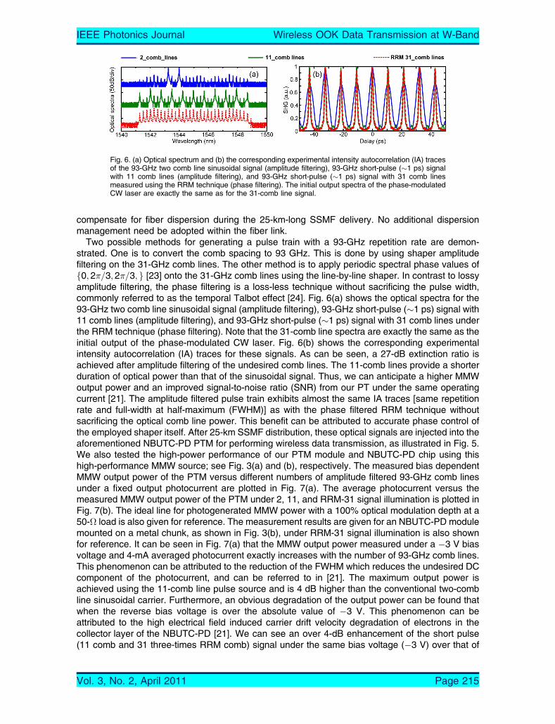
Two possible methods for generating a pulse train with a 93-GHz repetition rate are demon-strated. One is to convert the comb spacing to 93 GHz. This is done by using shaper amplitudefiltering on the 31-GHz comb lines. The other method is to apply periodic spectral phase values off0; 2�=3;2�=3; g [23] onto the 31-GHz comb lines using the line-by-line shaper. In contrast to lossyamplitude filtering, the phase filtering is a loss-less technique without sacrificing the pulse width,commonly referred to as the temporal Talbot effect [24]. Fig. 6(a) shows the optical spectra for the93-GHz two comb line sinusoidal signal (amplitude filtering), 93-GHz short-pulse (�1 ps) signal with11 comb lines (amplitude filtering), and 93-GHz short-pulse (�1 ps) signal with 31 comb lines underthe RRM technique (phase filtering). Note that the 31-comb line spectra are exactly the same as theinitial output of the phase-modulated CW laser. Fig. 6(b) shows the corresponding experimentalintensity autocorrelation (IA) traces for these signals. As can be seen, a 27-dB extinction ratio isachieved after amplitude filtering of the undesired comb lines. The 11-comb lines provide a shorterduration of optical power than that of the sinusoidal signal. Thus, we can anticipate a higher MMWoutput power and an improved signal-to-noise ratio (SNR) from our PT under the same operatingcurrent [21]. The amplitude filtered pulse train exhibits almost the same IA traces [same repetitionrate and full-width at half-maximum (FWHM)] as with the phase filtered RRM technique withoutsacrificing the optical comb line power. This benefit can be attributed to accurate phase control ofthe employed shaper itself. After 25-km SSMF distribution, these optical signals are injected into theaforementioned NBUTC-PD PTM for performing wireless data transmission, as illustrated in Fig. 5.We also tested the high-power performance of our PTM module and NBUTC-PD chip using thishigh-performance MMW source; see Fig. 3(a) and (b), respectively. The measured bias dependentMMW output power of the PTM versus different numbers of amplitude filtered 93-GHz comb linesunder a fixed output photocurrent are plotted in Fig. 7(a). The average photocurrent versus themeasured MMW output power of the PTM under 2, 11, and RRM-31 signal illumination is plotted inFig. 7(b). The ideal line for photogenerated MMW power with a 100% optical modulation depth at a50-� load is also given for reference. The measurement results are given for an NBUTC-PD modulemounted on a metal chunk, as shown in Fig. 3(b), under RRM-31 signal illumination is also shownfor reference. It can be seen in Fig. 7(a) that the MMW output power measured under a �3 V biasvoltage and 4-mA averaged photocurrent exactly increases with the number of 93-GHz comb lines.This phenomenon can be attributed to the reduction of the FWHM which reduces the undesired DCcomponent of the photocurrent, and can be referred to in [21]. The maximum output power isachieved using the 11-comb line pulse source and is 4 dB higher than the conventional two-combline sinusoidal carrier. Furthermore, an obvious degradation of the output power can be found thatwhen the reverse bias voltage is over the absolute value of �3 V. This phenomenon can beattributed to the high electrical field induced carrier drift velocity degradation of electrons in thecollector layer of the NBUTC-PD [21]. We can see an over 4-dB enhancement of the short pulse(11 comb and 31 three-times RRM comb) signal under the same bias voltage (�3 V) over that of
Fig. 6. (a) Optical spectrum and (b) the corresponding experimental intensity autocorrelation (IA) tracesof the 93-GHz two comb line sinusoidal signal (amplitude filtering), 93-GHz short-pulse (�1 ps) signalwith 11 comb lines (amplitude filtering), and 93-GHz short-pulse (�1 ps) signal with 31 comb linesmeasured using the RRM technique (phase filtering). The initial output spectra of the phase-modulatedCW laser are exactly the same as for the 31-comb line signal.
IEEE Photonics Journal Wireless OOK Data Transmission at W-Band
Vol. 3, No. 2, April 2011 Page 215

the sinusoidal signal (two combs) under a high output photocurrent (9 10 mA). Besides, the high-power performance of the NBUTC-PD chip is superior to that of the PTM module. As can be seen inFig. 7(b), the relationship between the output power and photocurrent of the reference PD-chip isclose to the ideal line and a further 2.7 dB higher than the PTMmodule under the same photocurrentand the same optical short pulse (31 three-times RRM comb) excitation [25]. Furthermore, thesaturation current of the reference PD chip is as high as over 35 mA and three times higher than thatof our PTM module. For this comparison, the PD-chip and PTM module is biased under theiroptimized operation point, i.e.,�2 V [25] and�3 V, respectively, in order to get the highest output RFpower. The difference in their optimized bias points can be attributed to that the device-heatingproblem in PTM module, as discussed latter, would induce significant inert-valley scattering and blurthe ballistic transport phenomenon of photogenerated electron. It thus causes that the photo-generated MMW power under �2 and �3 V is almost the same, as shown in Fig. 7(a). The superiorhigh-power performance of PD-chip to PTM module can be ascribed to the fact that the PD chip ismounted on the metal chunk, which provides much better heat-sinking than for the PTM modulesuspended in free space for low MMW coupling loss; see Fig. 3. In addition, for high-powermeasurement of the PD-chip, the lensed fiber is raised to get a more uniform optical field/photocurrent distribution, which should greatly benefit the PDs high-power performance [13], [25],[26]. However, for PTMmeasurement, the lensed fiber must be almost in contact with the backside ofthe NBUTC-PD in order to obtain stable light injection. Vibration of the raised lensed fiber will greatlydegrade the quality of data transmission. The superior high-power performance of our PD-chip toPTM module is mainly due to the better heat-sinking and more uniform photocurrent distribution inthe active area of the PD-chip. We can clearly see that the MMW power delivered by the PD-chipunder pulse excitation is close to the ideal line, which is calculated using an optical source with a100% modulation depth and an ideal PD. The estimated effective modulation depth of our lightsource is around 160% with a 4-dB enhancement in MMW power, as calculated by de-embeddingthe around 3-dB high-frequency roll-off in the O–E response of our PD-chip, as shown in Fig. 4(a)[25]. Fig. 5 shows the experimental setup for remote signal up-conversion and wireless datatransmission [27], [28]. The 20-Gbit/s data signal used for bias modulation in our PTM can betransmitted by use of the other optical wavelength instead of directly carried on the optical LO signaland then converted to electrical data using another PD at the base station. Thus, we can expecta long fiber transmission distance with less dispersion, as noted above. During the experiments,20-Gbit/s electrical data is used to directly swing the bias point of the PTM to mimic the case of theaforementioned remote up-conversion [28]. In our system, the receiver end is composed of anotherW-band horn antenna and a fast power detector (VDI diode) for detecting the envelope of receivedMMW power, as depicted in Fig. 5. The down-converted data-stream is further amplified, recorded,
Fig. 7. (a) Measured MMW output power of our PTM versus different numbers of amplitude filtered93-GHz comb lines under a 4-mA photocurrent and different reverse bias voltages. (b) MeasuredMMW output power versus photocurrent of our PTM under 2, 11, and RRM-31 signal excitation andthat of the reference NBUTC-PD chip under RRM-31 signal excitation. Measurement setups adoptedfor the PTM module and PD chip are shown in Fig. 2.
IEEE Photonics Journal Wireless OOK Data Transmission at W-Band
Vol. 3, No. 2, April 2011 Page 216

and analyzed by an IF amplifier, high-speed sampling scope, and error-detector, respectively. Fig. 8shows the measured back-to-back baseband response of the entire channel (after up/down-conversion). The dots in such figure represent the measured data points and the solid curve is justthe interconnected lines after smoothing. As can be seen, the baseband bandwidth of thedemonstrated channel is around 15 GHz, which may not only be limited by the IMB, as discussedbefore, but also the video bandwidth of the power detector. Fig. 9(a) shows the �log (BER) at20 Gbit/s (PRBS: 215 � 1) versus transmission distances measured under three different opticalexcitations (two, 11 and 31 three-times RRM comb lines). The corresponding 20-Gbit/s eye-patternsare given in Fig. 9(b)–(d). As can be seen, error-free 20-Gbit/s operations are achieved for a 20-cmwireless distance, 25-km fiber transmission distance, and optical short pulse (both 11 and 31 three-times RRM comb lines) excitation. Furthermore, the short pulse excitation offers a lower BERcompared with the sinusoidal signal excitation, due to the improved MMW output power
Fig. 9. Measured �log (BER) at 20 Gbit/s (PRBS: 215 � 1) versus transmission distances under threedifferent optical excitation schemes (2, 11, and 31 three-times RRM comb lines). The insets gives themeasured 20-Gbit/s eye-patterns for (a) two comb lines, (b) 11 comb lines, and (c) 31 three-times RRMcomb lines.
Fig. 8. Measured back-to-back IF frequency responses for the entire channel for wireless datatransmission.
IEEE Photonics Journal Wireless OOK Data Transmission at W-Band
Vol. 3, No. 2, April 2011 Page 217
performance, as shown in Fig. 7. The significant improvement in 20-Gbit/s BER performancecompared with our previous results [27] can be attributed to the increase in the bandwidth of thereceiver (fast power detector) and output power performance of our PTM under pulse excitation. Acomparison is made with the reported 16-QAM, OFDM, or differential phase shift keying (DPSK)modulation formats [4], [29], [30]. The reported OOK modulation formats here although havingextremely high transmission data rates (20 Gbit/s) will havemore serious problems with the multipatheffect and occupy a larger bandwidth for the same desired data rate. However, we just need areceiver with much more compact and simpler architecture for OOK data detection. By use of theadvanced InP-HEMT foundry, the complex modulation and de-modulation processes for 10-Gbit/squadrature phase shift keying (QPSK) data in a single chip for 125-GHz wireless transmission hasbeen demonstrated [31]. Compared with the reported OOK 10-Gbit/s data transmission [9], thissolution offers the same (10 Gbit/s) data rate with only one half the wireless bandwidth and reducedmultipath effect and offers a compact size of receiver. The progress in high-speed IC technology thusprovides an effective way to optimize tradeoffs between the total transmission data rate, occupiedwireless bandwidth, multipath effect, and the size of transreceiver module in the photonic wirelesslinking system.
4. ConclusionIn conclusion, in this work, we demonstrate an NBUTC-PD-based PTM with an extremely wide O–Ebandwidth (67–118 GHz) and very-high IMB (9 15 GHz). Thanks to the isolation of the IF modu-lation input and O–E output signals, and the accuracy of the adopted equivalent-circuit model, boththe O–E and IF modulation responses can be precisely optimized. Low coupling loss (G 2 dB) at theW-band from the planar dipole-based radiator to the WR-10 waveguide output port, and a highextinction ratio (9 33 dB) during IF modulation can also be simultaneously achieved. With this noveldevice 20-Gbit/s error-free OOK wireless OOK data transmission has been successfully achievedover a 25-km-long SSMF, with a dispersion precompensated high modulation depth (160%), shortoptical pulse (�1 ps) train, and an ultra-high repetition rate (93 GHz).
References[1] T. Yamada, M. Kano, K. Yamamoto, K. Hirota, and M. Hirose, BMultimedia virtual laboratory on the gigabit network,[ in
Proc. Int. Conf. Artif. Real Telexistence, Taipei, Taiwan, Oct. 25–27, 2000, vol. 10, pp. 98–103.[2] HDMI Licensing, LLC, Sunnyvale, CA. [Online]. Available: http://www.hdmi.org/index.aspx[3] K. Kawasaki, Y. Akiyama, K. Komori, M. Uno, H. Takeuchi, T. Itagaki, Y. Hino, Y. Kawasaki, K. Ito, and A. Hajimiri, BA
millimeter-wave intra-connect solution,[ in ISSCC Dig. Tech. Papers, San Francisco, CA, Feb. 7–11, 2010, pp. 414–416.[4] W. J. Jiang, C. T. Lin, L. Y. Wang He, C. C. Wei, C. H. Ho, Y. M. Yang, P. T. Shih, J. Chen, and S. Chi, B32.65-Gbps
OFDM RoF signal generation at 60 GHz employing an adaptive I/Q imbalance correction,[ presented at the 36th Eur.Conf. Optical Commun., Torino, Italy, Sep. 19–23, 2010, Paper Th.9.B.5.
[5] T. Nagatsuma, T. Takada, H.-J. Song, K. Ajito, N. Kukutsu, and Y. Kado, BMillimeter- and THz-wave photonicstowards 100-Gbit/s wireless transmission,[ presented at the IEEE Photonic Society’s 23rd Annu. Meeting, Denver,CO, Nov. 7–11, 2010, Paper WE4.
[6] M. J. Crisp, S. Sabesan, R. V. Penty, and I. H. White, BRadio over fiber distributed antenna networks,[ IEEE LEOSNewslett., vol. 23, no. 1, pp. 16–20, Feb. 2009.
[7] H.-C. Chien, A. Chowdhury, Z. Jai, Y.-T. Hsueh, and G.-K. Chang, BLong-reach 60-GHz Mm-wave optical-wirelessaccess network using remote signal regeneration and upconversion,[ in Proc. 34th ECOC, Brussels, Belgium,Sep. 21–25, 2008, pp. 137–138.
[8] A. Hirata, T. Furuta, H. Ito, and T. Nagatsuma, B10-Gb/s millimeter-wave signal generation using photodiode biasmodulation,[ J. Lightw. Technol., vol. 24, no. 4, pp. 1725–1731, Apr. 2006.
[9] A. Hirata, T. Minotani, and T. Nagatsuma, BMillimeter-wave photonics for 10-Gbit/s wireless links,[ in Proc. IEEE LEOSAnnu. Meeting, Glasgow, U.K., Nov. 10–14, 2002, vol. 2, pp. 477–478.
[10] E. Rouvalis, M. J. Fice, C. C. Renaud, and A. J. Seeds, BOptoelectronic detection of millimetre-wave signals withtravelling-wave uni-travelling carrier photodiodes,[ Opt. Express, vol. 19, no. 3, pp. 2079–2084, Jan. 2011.
[11] J.-W. Shi, Y.-S. Wu, and Y.-S. Lin, BNear-ballistic uni-traveling-carrier photodiode based V-band optoelectronic mixerswith internal up-conversion-gain, wide modulation bandwidth, and very high operation current performance,[ IEEEPhoton. Technol. Lett., vol. 20, no. 11, pp. 939–941, Jun. 2008.
[12] Y.-S. Wu and J.-W. Shi, BDynamic analysis of high-power and high-speed near-ballistic uni-traveling carrierphotodiodes at W-band,[ IEEE Photon. Technol. Lett., vol. 20, no. 13, pp. 1160–1162, Jul. 2008.
IEEE Photonics Journal Wireless OOK Data Transmission at W-Band
Vol. 3, No. 2, April 2011 Page 218

[13] J.-W. Shi, F.-M. Kuo, C.-J. Wu, C. L. Chang, C. Y. Liu, C.-Y. Chen, and J.-I. Chyi, BExtremely high saturation current-bandwidth product performance of a near-ballistic uni-traveling-carrier photodiode with a flip-chip bonding structure,[IEEE J. Quantum Electron., vol. 46, no. 1, pp. 80–86, Jan. 2010.
[14] F.-M. Kuo, H. Yen-Lin, J.-W. Shi, N.-W. Chen, W.-J. Jiang, C.-T. Lin, J. Chen, C.-L. Pan, and S. Chi, B12.5-Gb/swireless data transmission by using bias modulation of NBUTC-PD based W-band photonic transmitter-mixer,[presented at the Optical Fiber Commun., San Diego, CA, Mar. 21–26, 2010, Paper OThF7.
[15] H.-J. Tsai, N.-W. Chen, F.-M. Kuo, and J.-W. Shi, BFront-end design of W-band integrated photonic transmitter withwide optical-to-electrical bandwidth for wireless-over-fiber application,[ in Proc. IEEE Microw. Theory Tech. Int. Microw.Symp., Anaheim, CA, May 23–28, 2010, pp. 740–743.
[16] N.-W. Chen, H.-J. Tsai, F.-M. Kuo, and J.-W. Shi, BHigh-speed W-band integrated photonic transmitter for radio-over-fiber applications,[ IEEE Trans. Microw. Theory Tech., vol. 59, 2011, to be published.
[17] H.-P. Chuang and C.-B. Huang, BGeneration and delivery of 1-ps optical pulses with ultrahigh-rates over 25 km singlemode fiber by a spectral line-by-line pulse shaper,[ Opt. Express, vol. 18, no. 23, pp. 24 003–24 011, Nov. 2010.
[18] A. Hirata, M. Harada, and T. Nagatsuma, B120-GHz wireless link using photonic techniques for generation, modulation,and emission of millimeter-wave signals,[ J. Lightw. Technol., vol. 21, no. 10, pp. 2145–2153, Oct. 2003.
[19] A. Hirata, T. Kosugi, N. Meisl, T. Shibata, and T. Nagatsuma, BHigh-directivity photonic emitter using photodiodemodule integrated with HEMT amplifier for 10-Gbit/s wireless link,[ IEEE Trans. Microw. Theory Tech., vol. 52, no. 8,pp. 1843–1850, Aug. 2004.
[20] H. Ito, T. Ito, Y. Muramoto, T. Furuta, and T. Ishibashi, BRectangular waveguide output unitraveling-carrier photodiodemodule for high-power photonic millimeter-wave generation in the F-band,[ J. Lightw. Technol., vol. 21, no. 12,pp. 3456–3462, Dec. 2003.
[21] F.-M. Kuo, J.-W. Shi, H.-C. Chiang, H.-P. Chuang, H.-K. Chiou, C.-L. Pan, N.-W. Chen, H.-J. Tsai, and C.-B. Huang,BSpectral power enhancement in a 100-GHz photonic millimeter-wave generator enabled by spectral line-by-line pulseshaping,[ IEEE Photon. J., vol. 2, no. 5, pp. 719–727, Oct. 2010.
[22] R. W. Ridgway and D. W. Nippa, BGeneration and modulation of a 94-GHz signal using electrooptic modulator,[ IEEEPhoton. Technol. Lett., vol. 20, no. 8, pp. 653–655, Apr. 2008.
[23] C.-B. Huang and Y. C. Lai, BLoss-less pulse intensity repetition-rate multiplication using optical all-pass filtering,[ IEEEPhoton. Technol. Lett., vol. 12, no. 2, pp. 167–169, Feb. 2000.
[24] J. Azana and S. Gupta, BComplete family of periodic Talbot filters for pulse repetition rate multiplication,[ Opt. Express,vol. 14, no. 10, pp. 4270–4279, May 2006.
[25] C.-B. Huang, J.-W. Shi, F.-M. Kuo, H.-P. Chuang, and C.-L. Pan, BGreen and high-power photonic millimeter-wave(MMW) generator for remote generation at 124-GHz,[ presented at the Optical Fiber Commun., Los Angeles, CA,Mar. 6–10, 2011, Paper OThG6.
[26] M. Chtioui, A. Enard, D. Carpentier, S. Bernard, B. Rousseau, F. Lelarge, F. Pommereau, and M. Achouche, BHigh-performance uni-traveling-carrier photodiodes with a new collector design,[ IEEE Photon. Technol. Lett., vol. 20, no. 13,pp. 1163–1165, Jul. 2008.
[27] J.-W. Shi, F.-M. Kuo, H. J. Tsai, Y.-M. Hsin, N.-W. Chen, H.-C. Chiang, H.-P. Chuang, C.-B. Huang, and C.-L. Pan,B20-Gb/s on–off-keying wireless data transmission by using bias modulation of NBUTC-PD based W-band photonictransmitter-mixer,[ presented at the IEEE Int. Topical Meeting Microwave Photon., Montreal, QC, Canada, Oct. 5–8,2010, Paper WE3-3.
[28] F.-M. Kuo, J.-W. Shi, N.-W. Chen, C.-B. Huang, H.-P. Chuang, H.-J. Tsai, and C.-L. Pan, B20-Gb/s error-free wirelesstransmission using ultra-wideband photonic transmitter-mixer excited with remote distributed optical pulse train,[presented at the Optical Fiber Commun., Los Angeles, CA, Mar. 6–10, 2011, Paper OWT5.
[29] M. Weiss, A. Stohr, F. Lecoche, and B. Charbonnier, B27 Gbit/sec photonic wireless 60 GHz transmission systemusing 16-QAM OFDM,[ in Proc. IEEE Int. Topical Meeting Microw. Photon., Valencia, Spain, Oct. 14–16, 2009, pp. 1–3(post deadline).
[30] R.-W. Ridgway, D.-W. Nippa, and S. Yen, BData transmission using differential phase-shift keying on a 92 GHz carrier,[IEEE Trans. Microw. Theory Tech., vol. 58, no. 11, pp. 3117–3126, Nov. 2010.
[31] H. Takahashi, T. Kosugi, A. Hirata, K. Murata, and N. Kukutsu, B10-Gbit/s quadrature phase-shift-keying modulator anddemodulator for 120-GHz-band wireless links,[ IEEE Trans. Microw. Theory Tech., vol. 58, no. 12, pp. 4072–4078,Dec. 2010.
IEEE Photonics Journal Wireless OOK Data Transmission at W-Band
Vol. 3, No. 2, April 2011 Page 219


![P ER A N C A N G AN S IM ULAT O R M ODULASI D A N ...dapat dibedakan menjadi: amplitude shift keying (ASK), frequency shift keying (FSK), dan phase shift keying (PSK)[4]. Modulasi](https://static.fdocument.pub/doc/165x107/611834f1b748f604fe6b728a/p-er-a-n-c-a-n-g-an-s-im-ulat-o-r-m-odulasi-d-a-n-dapat-dibedakan-menjadi-amplitude.jpg)