
Datos de la población mundial 2013. (Population Reference Bureau) 2013 population-data-sheet spanish

Reference Sheet for C112 Hardware
Autumn 2016
1 Boolean Algebra, Gates and Circuits
Basic Operators Precedence : (strongest) ′, ·, + (weakest).
AND ·A B R
0 0 00 1 01 0 01 1 1
OR +A B R
0 0 00 1 11 0 11 1 1
NOT ′
A R
0 11 0
Simplification Rules
� AND and OR are associative, commutative and distributive.
� (A′)′
= A.
� A ·A′ = 0 and A + A′ = 1.
� A ·A = A and A + A = A.
� A · 0 = 0 and A + 1 = 1.
� A · 1 = A and A + 0 = A.
� (A + B)′
= A′ ·B′ and (A ·B)′
= A′ + B′ (De Morgan’s).
Note that:
� Each equation has a dual (swap AND with OR and 0 with 1).
� De Morgan’s holds for any number of terms.
GatesThere are 4 possible one-input and 16 possible two-input gates. NAND and NORare preferred (small and fast).
Analysing Circuits Work systematically, building up a formula or truth tablein stages.
Simplifying Circuits Use De Morgan’s:
Control and Data Variables E.g. in a multiplexer:
1

2 Combinatorial Circuits
Minterms and Maxterms
� Minterm: Boolean product term in which for each input, Ak, Ak or A′k
appears exactly once.
� Maxterm: Boolean sum term ....
Cannonical Forms
� Minterm Cannonical Form: Boolean sum of all minterms that ouput 1.
� Maxterm Cannonical Form: Boolean product of all maxterms that output 0.
Karnaugh Maps E.g.
Remember:
� Order (00, 01, 11, 10) is important.
� K-maps are cyclic.
� We might be able to make a considerable simplification by considering max-terms (0s) instead of minterms.
� Don’t cares (X) can be 0 or 1 - value depends on whether not they are circled.
Combinatorial Circuit Design Process
1. Generate the truth table.
2. Generate the Karnaugh map.
3. Find the minimal Boolean Expression:
(a) Read off the K-map.
(b) Factor out any common factors.
4. Draw the circuit.
5. Minimise to suit production method:
(a) Reduce size (e.g. replace OR, AND by NAND, NOR).
(b) Improve speed (reduce cycles).
6. Test the circuit (e.g. systematic testing, formal verificaiton).
3 Physical Implementation
Models of the Transistor Need to take into account a time delay.
1. Procedural model :
(a) G,Dand G,S not connected.
(b) If VGS < 0.5V: switch open.
(c) If VGS > 1.7V: switch closed.
2. Time Delay :
(a) It takes a constant time for the transistor to which states- can lead to spikes.
3. Change is not Instantaneous:
(a) Account for capacitance: I = C dV
dt.
Ideal change is 0 - 5V, but actually is somewhere close 0.2 - 3.7V (with 0.5 - 1.7Vconsidered non-deterministic).
2

Basic Gate ImplementationsNOT
NAND and NOR
Actual ICs generally use a combination of NMOS and PMOS (ComplimentaryMetal Oxide Silicon) instead of resistors - lower power consumption and fasterswitching.
Time Dependent Behaviour of Circuits
Noise Margin
Fan out The number of inputs to which the output of a gate is connected.
� Since 1R = 1
R1+ 1
R2+ . . . + 1
Rnfor n resistors in parallel, the load resistance
decreases as fan out increases, so output voltage falls.
� Slows down circuit since capacitance is summed accross all gates.
4 Synchronous Digital Systems
Feedback Circuit below could:
� Oscillate between values of 0 and 1.
� Settle at an intermediate value (actually ≈1.2V).
The R-S Flip Flop E.g. consider:
By considering all possible states for (RSPQ) and what they lead to in the fol-lowing time step:
3
� Uncertain about state at start (until set or reset).
� SR = 01: Resets memory (Q) to 0.
� SR = 10: Sets memory (Q) to 1.
� SR = 11: Keeps current state.
D-Type Latch Consider:
� If latch set to 1, Q becomes D.
� If latch set to 0, Q is held.
Edge Triggering D-type latch has undesirable behaviour. While latch is 1,any change on D changes Q:
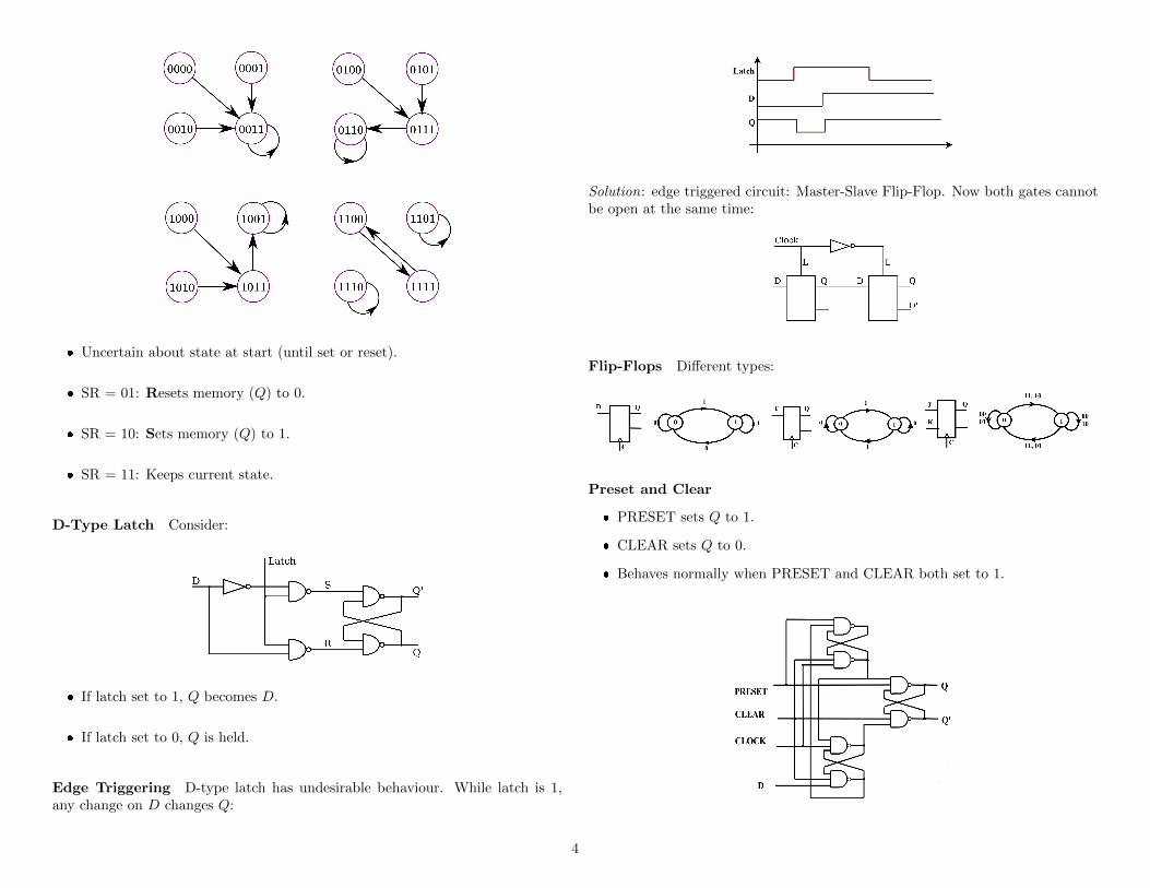
Solution: edge triggered circuit: Master-Slave Flip-Flop. Now both gates cannotbe open at the same time:
Flip-Flops Different types:
Preset and Clear
� PRESET sets Q to 1.
� CLEAR sets Q to 0.
� Behaves normally when PRESET and CLEAR both set to 1.
4

Synchronous Digital Systems
� Synchronous: Circuit only changes in response to system clock.
� Sequential : Goes through sequence of states.
General form:
� The state sequencing logic and output logic are combinatorial circuits.
� Outputs depend only on state of circuit.
� Next state depends on current state and inputs.
Sequential Circuit Design Process
1. Determine the required number of states and assign each output to a state.Adjacent assignments should be given to states if they:
(a) Have the same next state for a given input.
(b) Are the next states of the same state.
(c) Or choose to minimise output logic.
2. Determine the state transitions. Draw a state transition diagram and a statetransition table.
3. For each flip-flop input Dn, draw a Karnaugh Map and determine a Booleanexpression in terms of the flip-flop outputs and circuit inputs. Simplify.
4. Check don’t cares. Fix by one of these methods:
(a) Look at K-Maps and try to find a simple modification.
(b) Include unused states and redo.
5. Determine Boolean expressions for output from the state assignments, usingKarnaugh maps.
6. Draw and optimise the circuit. Remember common terms only need to becommitted to hardware once!
5 Functional Design
Shift Registers
� Inside a computer data is organised in a parallel form, but communicationusually involves serial data.
� Registers are an ordered group of flip-flops connected to a single clock.
� We can convert paralell and serial data.
� Time to load a parallel input depends on length of register.
� Requires a seperate (slower) clock to processor clock.
Multi-Function Registers Want to be able to shift bits left / right with thesame circuitry.
Here we can use 00 to hold, 01 to shift right, 10 to shift left, 11 to load parallel.
5
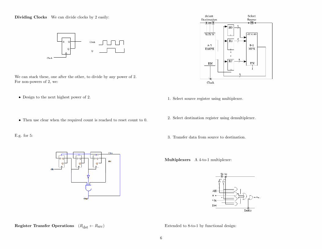
Dividing Clocks We can divide clocks by 2 easily:
We can stack these, one after the other, to divide by any power of 2.For non-powers of 2, we:
� Design to the next highest power of 2.
� Then use clear when the required count is reached to reset count to 0.
E.g. for 5:
Register Transfer Operations (Rdst ← Rsrc)
1. Select source register using multiplexer.
2. Select destination register using demultiplexer.
3. Transfer data from source to destination.
Multiplexers A 4-to-1 multiplexer:
Extended to 8-to-1 by functional design:
6

Demultiplexers A 2-to-4 demultiplexer:
Extended to 3-to-8 by functional design:
Comparators A 1-bit comparator:
Extended to 4-bit by functional design:
5.1 Computer Arithmetic
Half Adder S = A⊕B and C = A ·B:
A B Sum Carry
0 0 0 0
0 1 1 0
1 0 1 0
1 1 0 1
Full Adder Need to propogate the carry, S = A ⊕ B ⊕ C and Cout = C ·(A⊕B) + A ·B.
A B Cin S Cout
0 0 0 0 0
0 0 1 1 0
0 1 0 1 0
0 1 1 0 1
1 0 0 1 0
1 0 1 0 1
1 1 0 0 1
1 1 1 1 1
Ripple Through Carry Adder For n bits:
7

Serial Adder Assumes bits arrive least significant first.
Subtractor Difference = A⊕B ⊕ P and Borrow = A′ · (B ⊕ P ) + B · P :
A B P Difference Borrow
0 0 0 0 0
0 1 0 1 1
1 0 0 1 0
1 1 0 0 0
0 0 1 1 1
0 1 1 0 1
1 0 1 0 0
1 1 1 1 1
Subtractor using Two’s Complement A−B = A + (−B).
Multiplication a1a0 × b1b0 = a1 · b1 · 22 + a0 · b1 · 2 + a1 · b0 · 2 + a0 · b0.Multiplication by 2 is equivalent to a left shift, so for 2 bits:
Using functional design, for 4 bits:
Division
� Can be done procedurally using shifts and subtracts.
� Combinatorial hardware also exists.
8

The ALU A simple combinatorial circuit that bundles together arithmetic cir-cuits:
Requires two multiplexers per bit. Assuming the two subtractors and one adderare already in place:
Here we have the functions: A - constant 0, B - B − A, C - A− B, D - A + B,E - A⊕B, F - A + B, G - A ·B, H - constant 1.We can use functional design to extend the ALU to 8 bits:
The Shifter We can very easily design an eight function shifter:
Here we have the functions: A - unchanged, B - rotate left, C - arithmeticleft shift, D - left shift with carry, E - rotate right, F - logical right shift, G -arithmetic right shify, H - right shift with carry.
6 Processors
A Manual Processor Data Path Diagram
Instruction Format We define the instruction register hold instructions asfollows:
IR7 IR6 IR5 IR4 IR3 IR2 IR1 IR0
UN F/ALU-SHIFT UN S/R S/C S/A
� S/A selects input to A register.
� S/C selects input to “Carry in” of ALU.
� S/R selects input to RES-register.
� F/ALU determinse function of ALU/shifter. 000 for A, ..., 111 for H.
� Bits 3 and 7 are unused.
9
Execution Cycle
1. Load IR register.
2. Load A register.
3. Load B, C registers.
4. Load IR register.
5. Load RES, C registers.
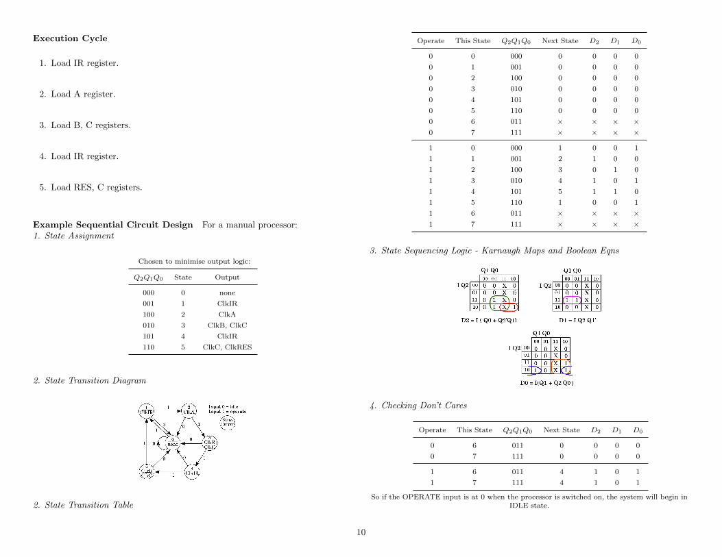
Example Sequential Circuit Design For a manual processor:1. State Assignment
Chosen to minimise output logic:
Q2Q1Q0 State Output
000 0 none
001 1 ClkIR
100 2 ClkA
010 3 ClkB, ClkC
101 4 ClkIR
110 5 ClkC, ClkRES
2. State Transition Diagram
2. State Transition Table
Operate This State Q2Q1Q0 Next State D2 D1 D0
0 0 000 0 0 0 0
0 1 001 0 0 0 0
0 2 100 0 0 0 0
0 3 010 0 0 0 0
0 4 101 0 0 0 0
0 5 110 0 0 0 0
0 6 011 × × × ×0 7 111 × × × ×
1 0 000 1 0 0 1
1 1 001 2 1 0 0
1 2 100 3 0 1 0
1 3 010 4 1 0 1
1 4 101 5 1 1 0
1 5 110 1 0 0 1
1 6 011 × × × ×1 7 111 × × × ×
3. State Sequencing Logic - Karnaugh Maps and Boolean Eqns
4. Checking Don’t Cares
Operate This State Q2Q1Q0 Next State D2 D1 D0
0 6 011 0 0 0 0
0 7 111 0 0 0 0
1 6 011 4 1 0 1
1 7 111 4 1 0 1
So if the OPERATE input is at 0 when the processor is switched on, the system will begin inIDLE state.
10

5. Output Logic - Karnaugh Maps and Boolean Eqns
*. Connecting Output to the System Clock
We use a NAND gate to connect each output to the system clock. This means the stateregister changes on the falling edge, avoiding race conditions when the next state is set on the
following rising edge.
We now have a manual processor!
Memory
� A D-type flip flop is a one bit memory.
� We need to give it an address (binary number). We use a demultiplexer todo this.
Buses E.g. address bus, data buses, control bus.
� Data-in and data-out are never used at the same time. Convenient to useone (bi-directonal) bus. This requires a tri-state buffer.
Tri-State Buffer If C is 0, ouput follows D, otherwise is disconnected com-pletely.
We can use a demultiplexer to make sure only one input has C set to 0.
Random Access Memory Normally organised in two dimensions with rowand column decoders.
� Each memory cell enabled when both row and column lines are 1.
� Only ever one such cell.
� Each cell connected to same read/write line and data line.
� Data line connected to outside through a two-way tri state buffer, so unlessthe chip is enabled, no data can pass in or our. Allows RAM with severalchips.
Connecting RAM to a Processor
� Need Memory Address Register (MAR) to store address.
� Memory Data Register (MDR) to store data read from memory / to bewritten to memory.
� Program counter (PC) stores address of next program instruction to be exe-cuted.
� Instruction register (IR) stores the program instruction executed.
11

Fetch Cycle To retrieve data from memory we go through register transfersteps. E.g. to get the next program instruction and load it into the IR:
1. MAR← PC
2. MDR← RAM [MAR], PC→ PC + 1
3. IR← MDR
Controller
� Sets multiplexers to establish required connection paths.
� Gives falling edge signal to clock inputs of registers to be loaded (done bygating system clock - NAND with clock control logic).
� Is a synchronous sequential circuit.
Dynamic RAM For large RAMs, D-Q flip flops are to big, instead one tran-sistor and capacitor is used for each bit. Value = whether capacitor is charged.
� Store is not permanent, ones drift to zero quickly.
� Capacitor charge is restored regularly, done by memory controller when thecomputer not accessing memory.
Speeding Up the Processor
� Change buses from 8 to 32 bit.
� Provide local registers which can be programmed to store partial results.
� Design a controller with as small a number of execution cycles as possible.
� Remove carry arrangments, doing arithmetic on big integers.
� Replace bi-directional data bus with seperate data in and data out buses.
Defining Operations E.g. LOAD, using register transfer language:
Instruction Cycle Transfers Path
LOAD Rdst, Addr
E1 MAR←MDR Via bit mask
E2 MDR←Memory
E3 Rdst←MDR No mask
Instruction format: 8 bits for the opcode, 4 for Rdest, 20 for address.
Designing the Controller
� Define a control input based on how many cycles required for each operation.
– Using 8-to-256 decoder to decode the opcode.
– Using 3-to-8 decoder for current state.
� Sequential design problem to work out next state, uses this control input andprevious state.
� Output logic:
– Clocks: NAND gates with system clock. In practice, we can simplifyoutput logic by considering the following cycle.
– Multiplexers and ALU / Shifter function selection output is trivial.
Possible Improvements
� Instructions packed on byte boundaries so not to waste fetch cycles.
� Additional arithmetic hardware.
� Additional multiplexers, e.g. to select input of B independently of A.
12