PRINCIPLES OF PLASMA PROCESSING - …ffchen/Publs/Chen208i.pdfLecture Notes on PRINCIPLES OF PLASMA...
6
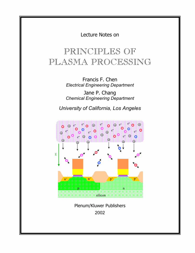
Lecture Notes on PRINCIPLES OF PLASMA PROCESSING Francis F. Chen Electrical Engineering Department Jane P. Chang Chemical Engineering Department University of California, Los Angeles e - e - e - e - e - e - + + + + + + + + e - e - e - e - e - + + + + + + + e - e - e - e - e - e - + + + + + + + + + + + + + + + + e - e - e - e - e - + + + + + + + + + + + + + + n p n + n + p + p + silicon E Plenum/Kluwer Publishers 2002
-
Upload
truongmien -
Category
Documents
-
view
225 -
download
0
Transcript of PRINCIPLES OF PLASMA PROCESSING - …ffchen/Publs/Chen208i.pdfLecture Notes on PRINCIPLES OF PLASMA...
Lecture Notes on
PRINCIPLES OFPLASMA PROCESSING
Francis F. ChenElectrical Engineering Department
Jane P. ChangChemical Engineering Department
University of California, Los Angeles
������������������������������������������������������������������������������������������������������������������������������������������������������������������������������������������������������������������������������������������������������������������������������������������������������������������������������������������������������������������������������������������������������������������������������������������������������������������������������������������������������������������������������������������������������������������������������������������������������������������������������������������������������������������������������������������������������������������������������������������������������������������������������������������������������������������������������������������������������������������������������������������������������
e-e- e-
e-
e-
e-+
+ +
+++
+ +
������������������������������������������������������������������������������������������������������������������������������������������������������������������������������������������������������������������������������������������������������������������������������������������������������������������������������������������������������������������������������������������������������������������������������������������������������������������������������������������������������������������������������������������������������������������������������������������������������������������������������������������������������������������������������������������������������������������������������������������������������������������������������������������������������������������������������������������������������������������������������������������������������������������
������������������������������������������������������������������������������������������������������������������������������������������������������������������������������������������������������������������������������������������������������������������������������������������������������������
��������������������������������������������������������������������������������������������������������������������������������������������������������������������������������������������������������������������������������������������������������������������������������������������������������
e-e- e-
e-
e-+
+ +
++
+ +
np
n+ n+ p+ p+
silicon
E
������������������������������������������������������������������������������������������������������������������������������������������������������������������������������������������������������������������������������������������������������������������������������������������������������������������������������������������������������������������������������������������������������������������������������������������������������������������������������������������������������������������������������������������������������������������������������������������������������������������������������������������������������������������������������������������������������������������������������������������������������������������������������������������������������������������������������������������������������������������������������������������������������
e-e- e-
e-
e-
e-++
++ ++
++++++
++ ++
������������������������������������������������������������������������������������������������������������������������������������������������������������������������������������������������������������������������������������������������������������������������������������������������������������������������������������������������������������������������������������������������������������������������������������������������������������������������������������������������������������������������������������������������������������������������������������������������������������������������������������������������������������������������������������������������������������������������������������������������������������������������������������������������������������������������������������������������������������������������������������������������������������������
������������������������������������������������������������������������������������������������������������������������������������������������������������������������������������������������������������������������������������������������������������������������������������������������������������
��������������������������������������������������������������������������������������������������������������������������������������������������������������������������������������������������������������������������������������������������������������������������������������������������������
e-e- e-
e-
e-++
++ ++
++++
++ ++
np
n+ n+ p+ p+
silicon
E
Plenum/Kluwer Publishers
2002
Preface v
Reference books used in this course
PRINCIPLES OF PLASMA PROCESSING
PREFACE
We want to make clear at the outset what this bookis NOT. It is not a polished, comprehensive textbook onplasma processing, such as that by Lieberman andLichtenberg. Rather, it is an informal set of lecture noteswritten for a nine-week course offered every two years atUCLA. It is intended for seniors and graduate students,especially chemical engineers, who have had no previousexposure to plasma physics. A broad range of topics iscovered, but only a few can be discussed in enough depthto give students a glimpse of forefront research. Sinceplasmas seem strange to most chemical engineers,plasma concepts are introduced as painlessly as possible.Detailed proofs are omitted, and only the essential ele-ments of plasma physics are given. One of these is theconcept of sheaths and quasineutrality. Sheaths aredominant in plasma �reactors,� and it is important to de-velop a physical feel for their behavior.
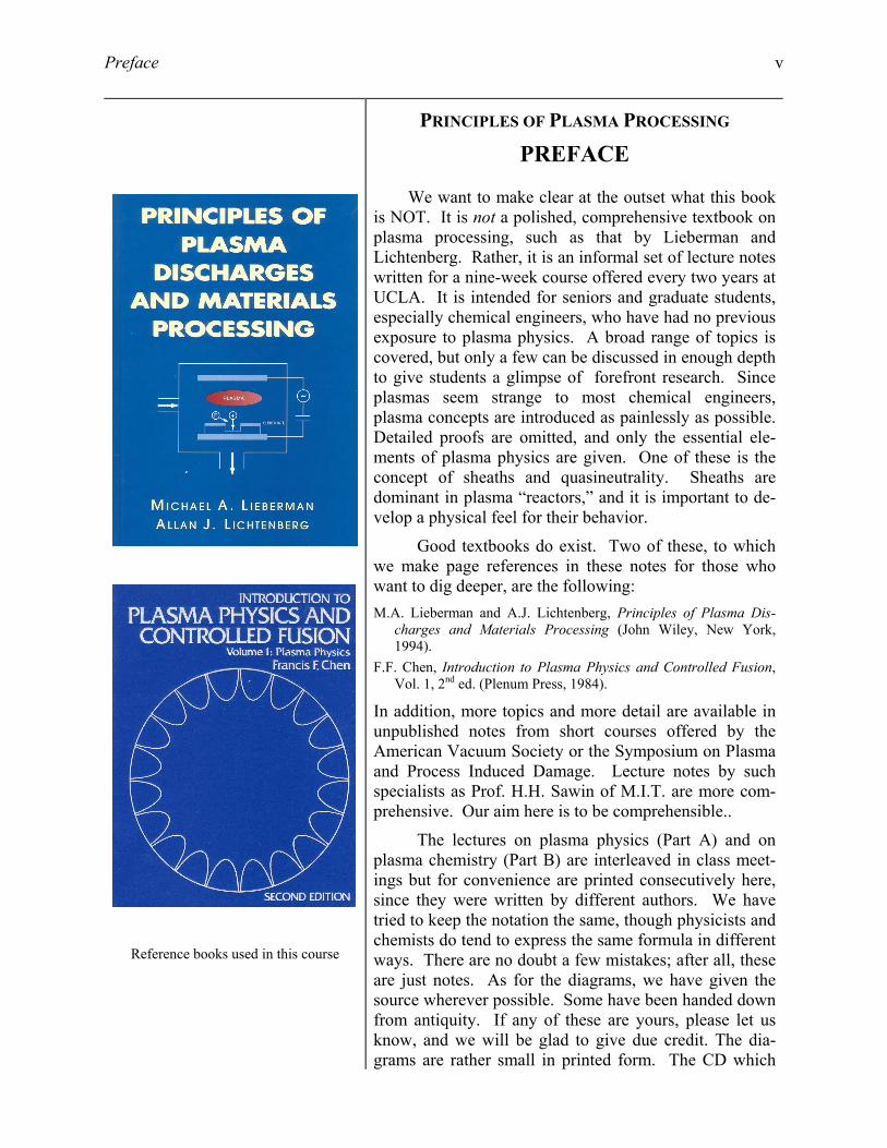
Good textbooks do exist. Two of these, to whichwe make page references in these notes for those whowant to dig deeper, are the following:M.A. Lieberman and A.J. Lichtenberg, Principles of Plasma Dis-
charges and Materials Processing (John Wiley, New York,1994).
F.F. Chen, Introduction to Plasma Physics and Controlled Fusion,Vol. 1, 2nd ed. (Plenum Press, 1984).
In addition, more topics and more detail are available inunpublished notes from short courses offered by theAmerican Vacuum Society or the Symposium on Plasmaand Process Induced Damage. Lecture notes by suchspecialists as Prof. H.H. Sawin of M.I.T. are more com-prehensive. Our aim here is to be comprehensible..
The lectures on plasma physics (Part A) and onplasma chemistry (Part B) are interleaved in class meet-ings but for convenience are printed consecutively here,since they were written by different authors. We havetried to keep the notation the same, though physicists andchemists do tend to express the same formula in differentways. There are no doubt a few mistakes; after all, theseare just notes. As for the diagrams, we have given thesource wherever possible. Some have been handed downfrom antiquity. If any of these are yours, please let usknow, and we will be glad to give due credit. The dia-grams are rather small in printed form. The CD which

vi
A small section of a memory chip.
Straight holes like these can be etchedonly with plasmas
accompanies the text has color figures that can be ex-panded for viewing on a computer monitor. There arealso sample homework problems and exam questionsthere.
Why study plasma processing? Because we can�tget along without computer chips and mobile phonesthese days. About half the steps in making a semicon-ductor circuit require a plasma, and plasma machines ac-count for most of the equipment cost in a �fab.� Design-ers, engineers, and technicians need to know how aplasma behaves. These machines have to be absolutelyreliable, because many millions of transistors have to beetched properly on each chip. It is amazing that this canbe done at all; improvements will certainly require moreplasma expertise. High-temperature plasmas have beenstudied for decades in connection with controlled fusion;that is, the production of electric power by creatingminiature suns on the earth. The low-temperature plas-mas used in manufacturing are more complicated be-cause they are not fully ionized; there are neutral atomsand many collisions. For many years, plasma sourceswere developed by trial and error, there being little un-derstanding of how these devices worked. With the vaststore of knowledge built up by the fusion effort, thesituation is changing. Partially ionized, radiofrequencyplasmas are being better understood, particularly with theuse of computer simulation. Low-temperature plasmaphysics is becoming a real science. This is the newfrontier. We hope you will join in the exploration of it.
Francis F. Chen Jane P. Chang Los Angeles, 2002
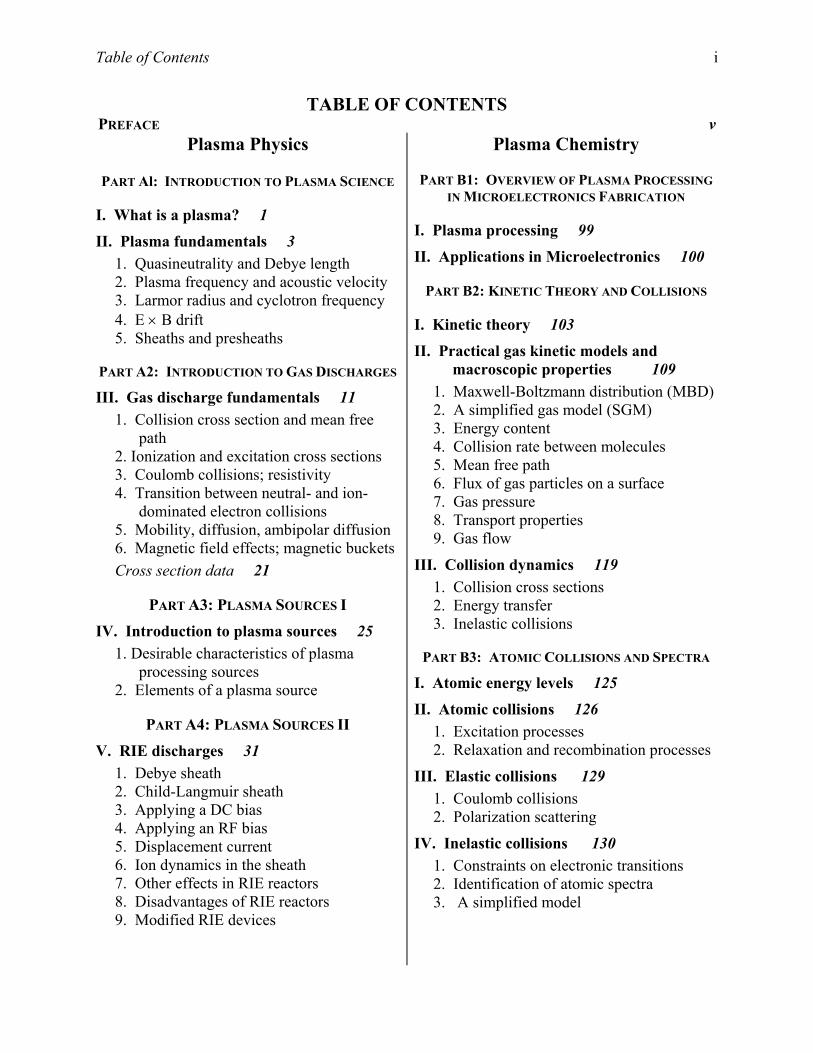
Table of Contents i
TABLE OF CONTENTSPREFACE v
Plasma Physics
PART Al: INTRODUCTION TO PLASMA SCIENCE
I. What is a plasma? 1II. Plasma fundamentals 3
1. Quasineutrality and Debye length2. Plasma frequency and acoustic velocity3. Larmor radius and cyclotron frequency4. E × B drift5. Sheaths and presheaths
PART A2: INTRODUCTION TO GAS DISCHARGES
III. Gas discharge fundamentals 111. Collision cross section and mean free
path2. Ionization and excitation cross sections3. Coulomb collisions; resistivity4. Transition between neutral- and ion-
dominated electron collisions5. Mobility, diffusion, ambipolar diffusion6. Magnetic field effects; magnetic bucketsCross section data 21
PART A3: PLASMA SOURCES I
IV. Introduction to plasma sources 251. Desirable characteristics of plasma
processing sources2. Elements of a plasma source
PART A4: PLASMA SOURCES II
V. RIE discharges 311. Debye sheath2. Child-Langmuir sheath3. Applying a DC bias4. Applying an RF bias5. Displacement current6. Ion dynamics in the sheath7. Other effects in RIE reactors8. Disadvantages of RIE reactors9. Modified RIE devices
Plasma Chemistry
PART B1: OVERVIEW OF PLASMA PROCESSINGIN MICROELECTRONICS FABRICATION
I. Plasma processing 99II. Applications in Microelectronics 100
PART B2: KINETIC THEORY AND COLLISIONS
I. Kinetic theory 103II. Practical gas kinetic models and
macroscopic properties 1091. Maxwell-Boltzmann distribution (MBD)2. A simplified gas model (SGM)3. Energy content4. Collision rate between molecules5. Mean free path6. Flux of gas particles on a surface7. Gas pressure8. Transport properties9. Gas flow
III. Collision dynamics 1191. Collision cross sections2. Energy transfer3. Inelastic collisions
PART B3: ATOMIC COLLISIONS AND SPECTRA
I. Atomic energy levels 125II. Atomic collisions 126
1. Excitation processes2. Relaxation and recombination processes
III. Elastic collisions 1291. Coulomb collisions2. Polarization scattering
IV. Inelastic collisions 1301. Constraints on electronic transitions2. Identification of atomic spectra3. A simplified model
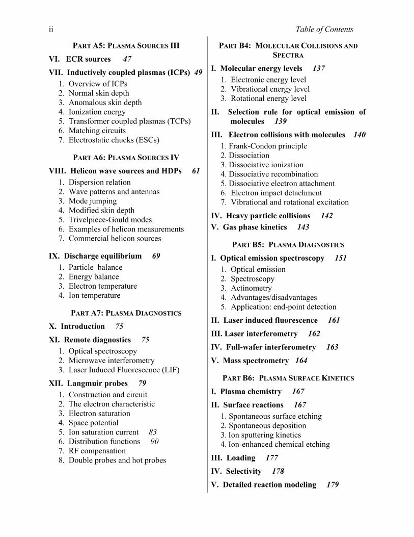
Table of Contentsii
PART A5: PLASMA SOURCES III
VI. ECR sources 47VII. Inductively coupled plasmas (ICPs) 49
1. Overview of ICPs2. Normal skin depth3. Anomalous skin depth4. Ionization energy5. Transformer coupled plasmas (TCPs)6. Matching circuits7. Electrostatic chucks (ESCs)
PART A6: PLASMA SOURCES IV
VIII. Helicon wave sources and HDPs 611. Dispersion relation2. Wave patterns and antennas3. Mode jumping4. Modified skin depth5. Trivelpiece-Gould modes6. Examples of helicon measurements7. Commercial helicon sources
IX. Discharge equilibrium 691. Particle balance2. Energy balance3. Electron temperature4. Ion temperature
PART A7: PLASMA DIAGNOSTICS
X. Introduction 75XI. Remote diagnostics 75
1. Optical spectroscopy2. Microwave interferometry3. Laser Induced Fluorescence (LIF)
XII. Langmuir probes 791. Construction and circuit2. The electron characteristic3. Electron saturation4. Space potential5. Ion saturation current 836. Distribution functions 907. RF compensation8. Double probes and hot probes
PART B4: MOLECULAR COLLISIONS ANDSPECTRA
I. Molecular energy levels 1371. Electronic energy level2. Vibrational energy level3. Rotational energy level
II. Selection rule for optical emission ofmolecules 139
III. Electron collisions with molecules 1401. Frank-Condon principle2. Dissociation3. Dissociative ionization4. Dissociative recombination5. Dissociative electron attachment6. Electron impact detachment7. Vibrational and rotational excitation
IV. Heavy particle collisions 142V. Gas phase kinetics 143
PART B5: PLASMA DIAGNOSTICS
I. Optical emission spectroscopy 1511. Optical emission2. Spectroscopy3. Actinometry4. Advantages/disadvantages5. Application: end-point detection
II. Laser induced fluorescence 161III. Laser interferometry 162IV. Full-wafer interferometry 163V. Mass spectrometry 164
PART B6: PLASMA SURFACE KINETICS
I. Plasma chemistry 167II. Surface reactions 167
1. Spontaneous surface etching2. Spontaneous deposition3. Ion sputtering kinetics4. Ion-enhanced chemical etching
III. Loading 177IV. Selectivity 178V. Detailed reaction modeling 179
Table of Contents iii
XIII. Other local diagnostics 931. Magnetic probes2. Energy analyzers3. RF current probe4. Plasma oscillation probe
PART B7: FEATURE EVOLUTION ANDMODELING
I. Fundamentals of feature evolution inplasma etching 183
II. Predictive modeling 185III. Mechanisms of profile evolution 186
1. Ion bombardment directionality2. Ion scattering within the feature3. Deposition rate of passivants4. Line-of-sight redeposition of products5. Charging of surfaces in the features
IV. Profile simulation 190V. Plasma damage 193
1. Contamination2. Particulates3. Gate oxide Damage − photon4. Gate oxide damage − electrical stress5. Lattice damage6. Post-etch corrosion
EPILOGUE: CURRENT PROBLEMS IN SEMICONDUCTOR PROCESSING 199I. Front-end challenges 199 1. High-k dielectrics 2. Metal gates
II. Back-end challenges 201 1. Copper metalllization 2. Interlayer dielectrics (ILDs) 3. Barrier materials
III. Patterning nanometer features 204 1. E-beam
2. Resist trimming
IV. Deep reactive etch for MEMS 205V. Plasma-induced damage 206VI. Species control in plasma reactors 207


![Plasma TelwinEnterprise Plasma 160 HF[1]](https://static.fdocument.pub/doc/165x107/55cf9702550346d0338f3edd/plasma-telwinenterprise-plasma-160-hf1.jpg)