Porti-M200C · Scanning Line Time(SLT) is the time to print one complete line using all strobes...
29
http://www.woosim.com T T h h e e r r m m a a l l P P r r i i n n t t i i n n g g M M e e c c h h a a n n i i s s m m Porti-M200C Operator’s Manual WOOSIM SYSTEMS Inc. Porti-M200C.
Transcript of Porti-M200C · Scanning Line Time(SLT) is the time to print one complete line using all strobes...

http://www.woosim.com
TThheerrmmaall PPrriinnttiinngg MMeecchhaanniissmm
Porti-M200C
OOppeerraattoorr’’ss MMaannuuaall
WWOOOOSSIIMM SSYYSSTTEEMMSS IInncc.. PPoorrttii--MM220000CC..

http://www.woosim.com 2
Copyright Porti-M200C is 2inch Thermal Printing Mechanism operator’s manual Copyright 2008 by Woosim Systems Inc. All rights reserved. The information contained in this manual is the property of Woosim Systems Inc. and may not be reproduced in whole or in part without the prior written permission of Woosims System Inc. Trademark
aa rreeggiisstteerreedd ttrraaddeemmaarrkk ooff WWoooossiimm SSyysstteemmss IInncc..
All other trademark is the properties of their respective companies. NNoottiiccee
The contents of this manual are subject to change without notice.
TToo ccoonnttaacctt oouurr TTeecchhnniiccaall SSuuppppoorrtt :: Tel : (+82-2) 2107-3700 Fax : (+82-2) 2107-3707 E-mail : [email protected] Address : #501, Daerung Technotown 3th,
448, Gasan-Dong, GeumChun-Ku, Seoul, Korea
http://www.woosim.com 3
Table of Contents IINNTTRROODDUUCCTTIIOONN Thermal Printing Mechanism.......................................................................................................................................... 1
Copyright .................................................................................................................................................................... 2
Trademark ................................................................................................................................................................... 2
a registered trademark of Woosim Systems Inc. ......................................................................................................... 2
GENERAL SPECIFICATION ........................................................................................................................................ 5
DESCRIPTION OF THE MECHANISM ...................................................................................................................... 6
MAIN FEATURES ........................................................................................................................................................... 6
1. INTERFACE CONNECTOR (FFC or FPC 30P) ...................................................................................................... 7
2. Thermal Print Head...................................................................................................................................................... 8
2.1 Outlines ..................................................................................................................................................................... 8
2.2 Maximum Conditions at 25 .................................................................................................................................. 8
2.3 Typical Printing Conditions (Ambient Temperature of Printhead : at 25) ............................................................ 8
2.4 Ambient Conditions .................................................................................................................................................. 9
2.5 Print Quality (at standard Conditions and Ambient Temperature of Printhead : 25) ............................................ 9
2.6 Printhead Life (at standard Conditions and Ambient Temperature of Printhead : 25) .......................................... 9
2.7 Operation Precautions ............................................................................................................................................. 11
(11) Print quality would be degraded if paper or ink residue were stuck on the heat element area. For such ....... 11
a case, please use applicator with alcohol to clean up. Do not use any material or equipment, which.................... 11
destroy the heat elements. .............................................................................................................................................. 11
2.8 ................................................................................................................................................................................. 13
2.8.1 Circuit Diagram ............................................................................................................................................... 13
2.8.2 Electrical characteristics of Circuit(VDD=4.75~5.25V) .................................................................................... 14
2.8.3 Electrical characteristics of Circuit(VDD=3.13~3.47V) .................................................................................... 15
2.8.4 Timing chart ..................................................................................................................................................... 16
2.8.5 THERMISTOR SPECIFICATION .................................................................................................................. 17
3. PAPER FEED MOTOR ............................................................................................................................................. 18
3.1 Ratings .................................................................................................................................................................... 18
3.2 Standard circuit ....................................................................................................................................................... 18
3.2 Electrical characteristics ......................................................................................................................................... 19
3.3 Mechanical Characteristics ..................................................................................................................................... 19
3.4 Environmental Performance ................................................................................................................................... 20
3.5 Excitation ( 2 phase, Full step ) .............................................................................................................................. 20
http://www.woosim.com 4
4. AUTO CUTTER ......................................................................................................................................................... 21
4.1. Cutting Specification ............................................................................................................................................. 21
4.2. Cutting performance (at the first stage, 20 degrees, 65%RH) ............................................................................... 21
4.3. Environmental condition........................................................................................................................................ 22
4.4. Motor ..................................................................................................................................................................... 22
4.5. Micro switch .......................................................................................................................................................... 22
4.6. Driver circuit .......................................................................................................................................................... 23
4.4. Pin SPEC. .............................................................................................................................................................. 24
5. PAPER END SENSOR ............................................................................................................................................... 25
5.1 Maximum rating ..................................................................................................................................................... 25
5.2 Electron-optical characteristics ............................................................................................................................... 25
5.3 Paper end sensor block diagram & recommend circuit........................................................................................... 26
5.4 Paper end sensor connector’s pin assignments ....................................................................................................... 26
6. Detect Switch ............................................................................................................................................................... 27
6.1 General spec............................................................................................................................................................ 27
6.2 ELECTRICAL SPECIFICATION .......................................................................................................................... 27
6.3 MECHANICAL SPECIFICATION ........................................................................................................................ 27
6.4. Pin SPEC. .............................................................................................................................................................. 28
6.5. Circuit Diagram & recommend circuit .................................................................................................................. 28
7. DIMENSIONS ............................................................................................................................................................ 29

http://www.woosim.com 5
IINNTTRROODDUUCCTTIIOONN GGEENNEERRAALL SSPPEECCIIFFIICCAATTIIOONN
Item Specification
Printing Method Direct thermal line printing
Print Width 56mm
Head Configuration (dots/line) 448
Dot Pitch 0.125 mm (8 dots/mm)
Printing Speed 200 mm/s (MAX)
Paper Width 56 ± 0.2 mm
Paper feed method Friction feed
Head temperature sensor Thermistor
Paper detection Reflecting photo-sensor
Average resistance 650 Ω ±3%
Number of strobes 2
External dimensions (W x D x H) 84.2x61.2x37 mm
Weight 182.5 g
Life/Reliability 50Km / 37,000,000 lines
Recommended paper TSP-F50US or equivalent
Input Power 24VDC/ MAX 3A

http://www.woosim.com 6
DDEESSCCRRIIPPTTIIOONN OOFF TTHHEE MMEECCHHAANNIISSMM
MMAAIINN FFEEAATTUURREESS
High speed up 200mm/sec (MAX) High resolution 8dots/mm, 203dpi Paper detection photo-sensor Life 50km Printed paper
The main characteristics of the Porti-M200C thermal printing mechanism are definitely the reliability, the quality and the long lasting performance, making it the suitable product for industrial environments such as weighting, control, safety systems, as well as medical and portable applications.

http://www.woosim.com 7
11.. IINNTTEERRFFAACCEE CCOONNNNEECCTTOORR ((FFFFCC oorr FFPPCC 3300PP))
PIN NO. PIN NAME SECTION NOTE
1 DETECT Detect Switch
2 GND Public Use
3 PA-SEN2 Paper Sensor
4 PA-SEN1
5 VH
Printer Head
Public Use
6 VH
7 DO1
8 DI1
9 GND Public Use
10 GND Public Use
11 STB1
12 CLK
13 /LAT
14 VDD
15 TM
16 TM
17 STB2
18 GND Public Use
19 GND Public Use
20 DO2
21 DI2
22 VSF
23 VH Public Use
24 CT_SEN
Auto Cutter
25 CT2
26 CT1
27 PA
Motor
28 PNB
29 PB
30 PNA
Connector for FPC (pitch 1.25mm) such as yeonho connector series 12511HS-30 : Recommend applicable 1.25mm Pitch 30p FFC or FPC Cable

http://www.woosim.com 8
22.. TThheerrmmaall PPrriinntt HHeeaadd
22..11 OOuuttlliinneess
*1 Average resistance value is the one obtained as averaged resistance value of each heat element of the printhead.
Tolerance ±3% shows the distribution of such averaged resistance value of the printhead.
22..22 MMaaxxiimmuumm CCoonnddiittiioonnss aatt 2255
22..33 TTyyppiiccaall PPrriinnttiinngg CCoonnddiittiioonnss ((AAmmbbiieenntt TTeemmppeerraattuurree ooff PPrriinntthheeaadd :: aatt 2255)) * Mechanical Conditions
* Thermal Paper use for Evaluation - OJI KF50-HAD or Equivalent (Note 1)
Heat Elements Structure : 2 heater/dot Number of Heat Elements : 448 dots Heat Element Pitch : 0.125mm (8 dots/mm) Pitch Width : 56mm ± 0.2mm Average Resistance Value(Rave) *1 : 650 Ω ±3% Circuit Diagram : Fig. 2.8 Electrical Characteristics of Circuit : Table 2.8, Fig 2.8.3 Thermistor : Table 2.8.4, Fig 2.8.4
Item Symbol Maximum Conditions Unit Conditions
Supply Voltage VH 26.4 V Vp < 28V
Vp:peak of VH
Supply Energy EO 0.17
mJ/dot S.L.T = 0.5msec
0.25 S.L.T = 0.82msec
Substrate Temperature Tsub 65 Thermistor Temperature
Logic Supply Voltage V DD 7 V Include Peak Voltage
Logic Input Voltage V in -0.5 ~ V DD+ 0.5 V
((TTaabbllee 22..22))
Item Mechanical Conditions Unit or Conditions
Platen Pressure 14.7 ±1.96 N/print width
Platen Hardness 40 ±5 Shore A
Platen Diameter 15.0~20 mm
Scanning Resolution 8.0 line/mm
((TTaabbllee 22..33..11))

http://www.woosim.com 9
* Electrical Conditions (Note 2)
Item Symbol Electrical Conditions Unit Conditions
Power Consumption PO 0.79 W/dot Rave = 650Ω Supply Voltage VH 24 V
Print Cycle S.L.T 0.5 0.82 ms/line Ambient Temp
Energy Consumption (On Time)
EO (Ton)
0.16 0.20 mJ/dot 5
(0.202) 0.252 ms
0.15 0.19 mJ/dot 25
(0.189) 0.240 ms
0.14 0.18 mJ/dot 45
(0.177) 0.227 ms
Supply Current IO 15.6(*2) A ON at same time Print Segment 1 448dots
*2 The peak of current is 15.6A. The mean of current can’t be controlled to exceed the current capacity.
22..44 AAmmbbiieenntt CCoonnddiittiioonnss
22..55 PPrriinntt QQuuaalliittyy ((aatt ssttaannddaarrdd CCoonnddiittiioonnss aanndd AAmmbbiieenntt TTeemmppeerraattuurree ooff PPrriinntthheeaadd :: 2255))
(1) Optical Density Min.1.0 *3 (2) Variation of Density(Difference in printing intensity of all black) : Max.0.3 *3 *3 with Macbeth Densitometer RD-914
22..66 PPrriinntthheeaadd LLiiffee ((aatt ssttaannddaarrdd CCoonnddiittiioonnss aanndd AAmmbbiieenntt TTeemmppeerraattuurree ooff PPrriinntthheeaadd :: 2255)) End of Lifetime should be measured when the resistance value of each resistance element changes more than 15% compared with its initial value. Printing percentage at that time should be 12.5%
(1) Pulse Life 5´107 pulses (2) Abrasion Life 50Km
Item Symbol Ambient Conditions Unit on Conditions
Storage Temp Tsto -25 ~ 70
Operation Temp Tope 5 ~ 45
Humidity - 10 ~ 90 % RH No Condensation
((TTaabbllee 22..33..22))
((TTaabbllee 22..44))
http://www.woosim.com 10
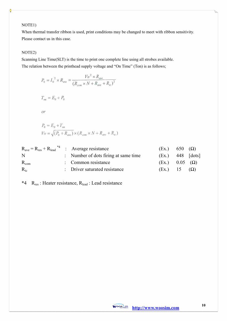
NOTE1) When thermal transfer ribbon is used, print conditions may be changed to meet with ribbon sensitivity. Please contact us in this case. NOTE2) Scanning Line Time(SLT) is the time to print one complete line using all strobes available. The relation between the printhead supply voltage and “On Time” (Ton) is as follows;
Rave = Rres + Rlead *4 : Average resistance (Ex.) 650 (Ω) N : Number of dots firing at same time (Ex.) 448 [dots] Rcom : Common resistance (Ex.) 0.05 (Ω) Ric : Driver saturated resistance (Ex.) 15 (Ω) *4 Rres : Heater resistance, Rlead : Lead resistance

http://www.woosim.com 11
22..77 OOppeerraattiioonn PPrreeccaauuttiioonnss
(1) When continuous printing is performed, the supply energy should be reduced so that the substrate temperature monitored through the thermistor will remain below the maximum temperature show in Section 2.(Maximum Conditions at 25 degrees C)
(2) Power on and off sequence must be in the following order to prevent the dot element damage; Turn on - Apply the logic supply voltage(VDD) first, before the print supply voltage(VSF,VH). (VSF, VH : Applide at the same timing) Turn off - Switch off the print supply voltage(VSF,VH) first, before turn the logic supply voltage(VDD) off. (VH, VSF :Switch off at the same timing)
(3) Interface each signal input (CLK, LAT, STB, DI) with CMOS level (ex. 74HC240). Please keep STB signal to “Disable” during ON/OFF and during no printing condition.
(4) When measuring resistance value of Heat element, VSF, and VH should be separated. As for applying voltage to VSF, Please refer to table 2.8.1,2.8.2
(5) Heat elements and IC’s shall be anti-electrostatic in order to prevent the electrostatic destruction. Do not touch the connector pins by naked hands.
(6) The printhead substrate surface is coated with glass and mechanical stress or shock (including dust scratch damage) should be avoided to prevent damage.
(7) When the printhead operation is finished, print supply voltage. (including the charged voltage with capacitor) should be reduced to the ground level and remained until next printhead operation.
(8) Platen roller should be composed of non-conductive materials. (9) Condensation should be avoided. If condensation occurred, do not switch on the printhead power until
condensation disappeared. (10) Tne connectors installed are connected directly to the substrate. Please pay attention to the extra
forces to get damages when the connector is plugged in or out. (Plug in-out cycle for this connector shall not be exceeded 20 times.)
(11) Print quality would be degraded if paper or ink residue were stuck on the heat element area. For such a case, please use applicator with alcohol to clean up. Do not use any material or equipment, which destroy the heat elements.
(12) If printing sound, for example sticking sound, occurred, please review and adjust the paper feed mechanism and the electrical pulse program to eliminate the sound.
(13) The change of printhead flatness (warp) is minimized with temperature change in the free body of one uint. Please pay attention to the warp created by fixing the printhead to the printer unit with screws or clamp.
(14) Please ensure that the paper used does not include bad element factor to affect the printhead life. (15) Printing without paper (Thermal paper etc.) should not be done. It may cause destruction on heat due
to overload. (16) If printhead operation method is changed, Please inform us in advance to change.
(17) In order to avoid surge, VH and GND cable length should be less than 100mm, and aluminum capacitor is required between VH and GND at controller board side. Ceramic capacitor should be

http://www.woosim.com 12
placed between VDD and GND. (18) Please design the component in such a way that the printing media (while in printing) and the paper
guide do not contact the IC protective coating and the pin protective coating, in order to keep the printing quality.
(19) Please make designing in such a way to avoid the contact with conductive components like head support plate, because there is an area where the electrode are exposed on the surface and the side of thermal printhead.
(20) Thermal printhead is heat-generating device, so that it may cause heat element damage or smoke / fire on its components by over heating if there occurs mechanical or electrical abnormalities. So please be sure to perform temperature control by thermistor and also to design the power(VH, VDD) shutdown system when abnormalities take place to protect the printhead.
(21) It dusts/foreign particles stuck on the surface of thermal head substrate or printed circuit board, it may cause stained print, faded print and also damage of heat element, smoking and combustion. In this case, the head should be cleaned by ethyl-alcohol after power source for head is shut down and please check if the dusts/foreign articles are completely removed. Yet, make sure that ethyl-alcohol is dried up before restarting the operation.
(22) Please design power source for head (VH, VDD) to be shutdown when the thermal head surpasses the maximum rated wattage while STB is On, or the printing media does not move like paper jam.
Otherwise, heated printing media bums and sticks to the head and may lead to combustion in the worst case.
http://www.woosim.com 13
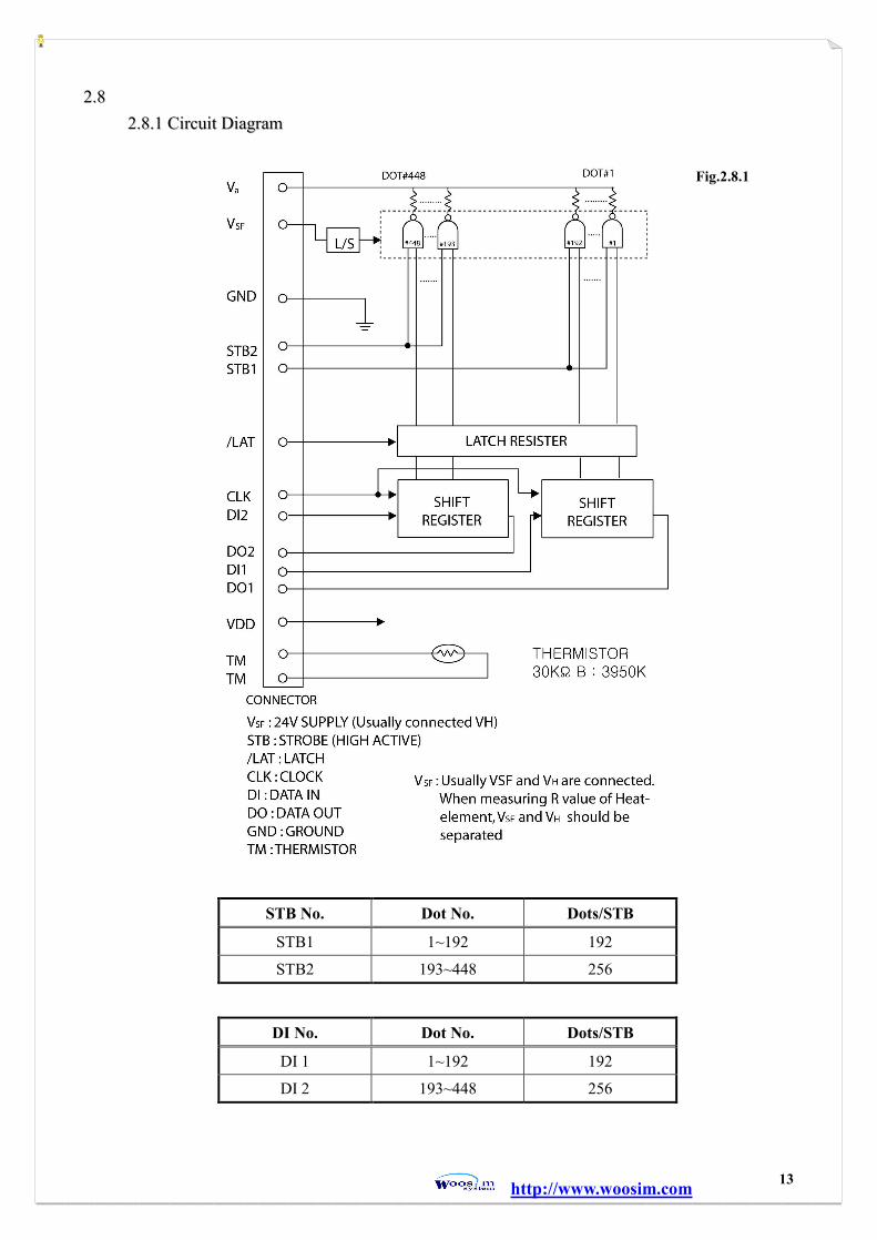
22..88 22..88..11 CCiirrccuuiitt DDiiaaggrraamm
Fig.2.8.1
STB No. Dot No. Dots/STB
STB1 1~192 192
STB2 193~448 256
DI No. Dot No. Dots/STB
DI 1 1~192 192
DI 2 193~448 256

http://www.woosim.com 14
22..88..22 EElleeccttrriiccaall cchhaarraacctteerriissttiiccss ooff CCiirrccuuiitt((VVDDDD==44..7755~~55..2255VV)) Table2.8.1
Ta=25 ±10
ITEM SYMBOL MIN. TYP. MAX. UNIT SIGNAL
PRINT VOLTAGE VH - 24.0 26.4 V
VSF VOLTAGE VSF 21.6 24.0 26.4 V
VSF CUREENT ISF - - 16 mA VSF=24.0V
LOGIC VOLTAGE VDD 4.75 5.00 5.25 V
LOGIC CURRENT IDD - - 160 mA fDI=fCLK/2
INPUT VOLTAGE
H VIH 0.8VDD - VDD V STB, DI, LAT, CLK
L VIL 0 - 0.2VDD V
DATA INPUT CURRENT (DI)
H IIH DI - - 0.5 VIH=5V
L IIL DI - - -0.5 VIL=0V
STB INPUT CURRENT (HIGH
ACTIVE)
H IIH STB - - 121
L IIL STB - - -2.0
CLOCK INPUT CURRENT (CLK)
H IIH CLK - - 2.0
L IIL CLK - - -2.0
LATCH INPUT CURRENT
(LAT)
H IIH LAT - - 2.0
L IIL LAT - - -2.0
DO VOLTAGE (DO)
H VDOH 4.6 - - V VDD =5V, IOH=-0.4
L VDOL - - 0.4 V VDD =5V, IOL=0.4
CLOCK FREQUENCY f CLK - - 16
SEE Fig. 2.8.2
CLOCK WIDTH tw CLK 30 - -
DATA SET-UP TIME tsetup DI 10 - -
DATA HOLD TIME thold DI 10 - -
DATA OUT DELAY TIME
td DO - - 53
LAT WIDTH tw LAT 100 - -
LAT SET-UP TIME tsetup LAT 100 - -
LAT HOLD TIME thold LAT 50 - -
STB SET-UP TIME tsetup STB 200 - -
DRIVER OUT DELAY TIME
Tdo - - 10

http://www.woosim.com 15
22..88..33 EElleeccttrriiccaall cchhaarraacctteerriissttiiccss ooff CCiirrccuuiitt((VVDDDD==33..1133~~33..4477VV)) Table2.8.2
Ta=25 ±10
ITEM SYMBOL MIN. TYP. MAX. UNIT SIGNAL
PRINT VOLTAGE VH - 24.0 26.4 V
VSF VOLTAGE VSF 21.6 24.0 26.4 V
VSF CUREENT ISF - - 16 mA VSF=24.0V
LOGIC VOLTAGE VDD 3.13 3.30 3.47 V
LOGIC CURRENT IDD - - 56 mA fDI=fCLK/2
INPUT VOLTAGE
H VIH 0.8VDD - VDD V STB, DI, LAT, CLK
L VIL 0 - 0.2VDD V
DATA INPUT CURRENT (DI)
H IIH DI - - 0.5 VIH=3.3V
L IIL DI - - -0.5 VIL=0V
STB INPUT CURRENT (HIGH
ACTIVE)
H IIH STB - - 80
L IIL STB - - -2.0
CLOCK INPUT CURRENT (CLK)
H IIH CLK - - 2.0
L IIL CLK - - -2.0
LATCH INPUT CURRENT
(LAT)
H IIH LAT - - 2.0
L IIL LAT - - -2.0
DO VOLTAGE (DO)
H VDOH 2.9 - - V VDD =3.3V, IOH=-0.4
L VDOL - - 0.4 V VDD =3.3V, IOL=0.4
CLOCK FREQUENCY f CLK - - 10
SEE Fig. 2.8.2
CLOCK WIDTH tw CLK 30 - -
DATA SET-UP TIME tsetup DI 10 - -
DATA HOLD TIME thold DI 10 - -
DATA OUT DELAY TIME
td DO - - 90
LAT WIDTH tw LAT 100 - -
LAT SET-UP TIME tsetup LAT 100 - -
LAT HOLD TIME thold LAT 50 - -
STB SET-UP TIME tsetup STB 200 - -
DRIVER OUT DELAY TIME
Tdo - - 10
http://www.woosim.com 16
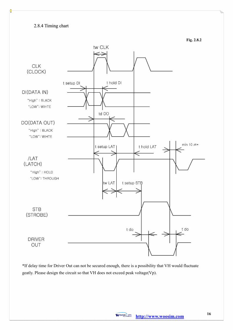
22..88..44 TTiimmiinngg cchhaarrtt
Fig. 2.8.2
*If delay time for Driver Out can not be secured enough, there is a possibility that VH would fluctuate geatly. Please design the circuit so that VH does not exceed peak voltage(Vp).

http://www.woosim.com 17
22..88..55 TTHHEERRMMIISSTTOORR SSPPEECCIIFFIICCAATTIIOONN
ELECTRICAL REQUIREMENTS;
1) RESISTANCE R25 : 30 ±5% at 25 2) B VALUE : 3950 ±2% 3) RESISTANCE vs. TEMPERATURE : Fig. 2.8.3 RATING; 1) OPERATING TEMPERATURE : -20 ~ +80 2) TIME CONSTANT : Max. 30sec(in the air)
Fig. 2.8.3 Temperature characteristic of Thermistor
RX=R25*EXPB*(1/TX-1/T25) (T; ABSOLUTE TEMPERATURE)
http://www.woosim.com 18
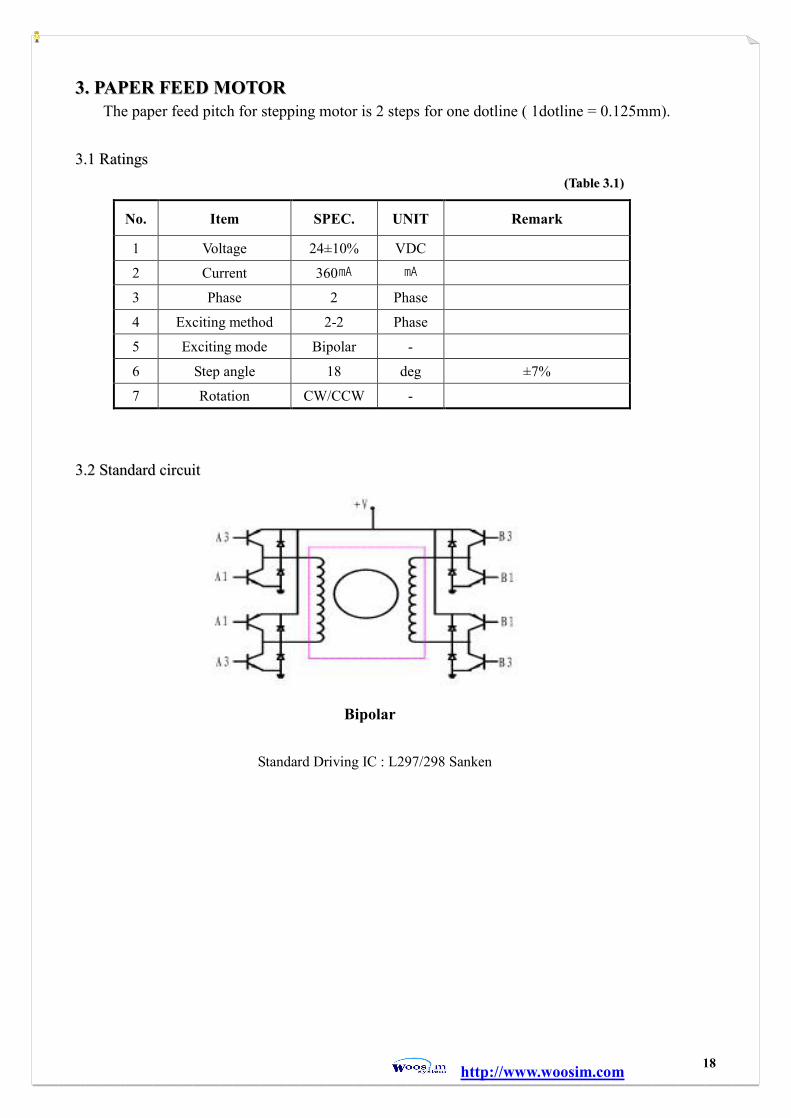
33.. PPAAPPEERR FFEEEEDD MMOOTTOORR The paper feed pitch for stepping motor is 2 steps for one dotline ( 1dotline = 0.125mm).
33..11 RRaattiinnggss ((TTaabbllee 33..11))
33..22 SSttaannddaarrdd cciirrccuuiitt
No. Item SPEC. UNIT Remark
1 Voltage 24±10% VDC
2 Current 360
3 Phase 2 Phase
4 Exciting method 2-2 Phase
5 Exciting mode Bipolar -
6 Step angle 18 deg ±7%
7 Rotation CW/CCW -
Bipolar
Standard Driving IC : L297/298 Sanken

http://www.woosim.com 19
33..22 EElleeccttrriiccaall cchhaarraacctteerriissttiiccss
33..33 MMeecchhaanniiccaall CChhaarraacctteerriissttiiccss
((TTaabbllee 33..22))
No. ITEM SPEC. UNIT TEST CONDITION REMARK
1 Resistance 20±7% Ω At 25 Each phase
2 Inductance 9 mH At 25 1kHz, 1Vrms Each phase
3 Max. starting pulse rate 1200 min pps Standard operating condition
Continuous driving, by 10 pps increment 4 Max. response pulse rate 2000 min pps
5 Holding Torque 90 min gf.cm
6 Pull out torque 80 min gf.cm 24V 360 at 800pps
7 Dielectric Strength 3 max 500VAC, 1second
8 Insulation Resistance 100 min 500VDC
9 Insulation class Coil Class E Between case and coil
10 Temp. rise 115 max
Motor is fix on an standard plank, free load, normal temperature/humidity, 800pps driving, resistance method
((TTaabbllee 33..33))
No. ITEM SPEC. TEST CONDITION REMARK
1 Detent Torque 14gf.cm Each terminal opened no excitation
2 Appearance No damage and discoloration which may cause failure at standard operating conditions, if necessary, submit the limit sample which is obided by each other.
3 Mass 25.2g Measured by electronic
scale
4 Out put device With a output gear
5 Noise 50dB max 7.5VDC 800pps driving, free load, measured
10 from the motor
6 Out shaft thrust 0.5 max At the tip of out shaft
7 Out shaft deflection 0.05 max 5mm from the tip of out shaft
http://www.woosim.com 20
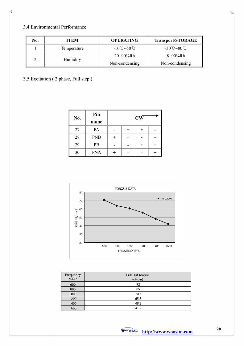
33..44 EEnnvviirroonnmmeennttaall PPeerrffoorrmmaannccee
33..55 EExxcciittaattiioonn (( 22 pphhaassee,, FFuullll sstteepp ))
No. ITEM OPERATING Transport/STORAGE
1 Temperature -10~50 -30~80
2 Humidity 20~90%Rh
Non-condensing 8~90%Rh
Non-condensing
No. Pin
name CW
27 PA - + + - 28 PNB + + - - 29 PB - - + + 30 PNA + - - +

http://www.woosim.com 21
44.. AAUUTTOO CCUUTTTTEERR The cutter is a thermal recording paper with its wide 63mm and thickness 65~100 in full or partial cut. 44..11.. CCuuttttiinngg SSppeecciiffiiccaattiioonn 4.1.1 Cutting method : Slide blade type
4.1.2 Media to be cut : 65µ thickness thermal recording paper 100µ thickness thermal recording paper
4.1.3 Effective cutting width : 63mm 4.1.4 Direction of paper curl : Paper curl should be in the direction of the stationary blade side. In case of paper curl to the direction of the movale blade side. The user should firmly assure the paper
pass under the actual cutting condition. 4.1.5 Weight : 100g approximately
44..22.. CCuuttttiinngg ppeerrffoorrmmaannccee ((aatt tthhee ffiirrsstt ssttaaggee,, 2200 ddeeggrreeeess,, 6655%%RRHH)) 4.2.1 Rated cutting time Less than 600msec
Voltage : DC24V±10% (between motor terminals) 4.2.2 Rated motor voltage : DC24V 4.2.3 Drive voltage range
DC24V±10% (voltage between motor terminals) Caution : not driving circuit voltage but voltage between motor terminals.
4.2.4 Start current : 1.2A max. (at DC 24V)
4.2.5 Insulation resistance : More than 1 min. (between the motor terminal and the cutter frame at 100VDC. 20 degrees, 65%RH)
4.2.6 Insulation voltage : 100VAC, 1min (between the motor terminal and the cutter frame.) 4.2.7 Cutting frequency : Less than 30cut/min. (more than 2 sec/cycle) 4.2.8 Cutter life
Target : 1million cuts at TF50KS-E2D (65µm thick thermal paper) To be determined after estimation

http://www.woosim.com 22
44..33.. EEnnvviirroonnmmeennttaall ccoonnddiittiioonn 4.3.1 Operating temp/humidity range
0~50 5%RH~80%RH Humidity condition (40 or over) 4.3.2 Storage environmental
Temperature : -25~70 Humidity : 5%RH~90%RH
44..44.. MMoottoorr : NF183G-1010017(Johnson Electric world trade Ltd.) : Rated driving voltage (between motor terminals)
DC 24V (operation voltage range DC24V±10%) : Start current : Less than 1.2A
44..55.. MMiiccrroo sswwiittcchh Micro switch : MLS1-AVS (Shimnel Electrionics) Rated contact point
a) rated voltage : DC5V b) rated current : 0.1mA (Specified current range : 0.04-100mA) c) Chattering : less than 10msec

http://www.woosim.com 23
44..66.. DDrriivveerr cciirrccuuiitt 4.4.1 Example 1 The drive circuit should be based on he principle shown below.
① Turn off the relay by command pulse. And apply voltage between the motor terminals. ② The switch built in the cutter turns off.(Provide a wait time of 10msec.) ③ Turn off the command pulse. ④ The switch built in the cutter turns on. ⑤ The motor stops.
Apply a braking force by short-circuiting the motor terminals concurrently with the turning-on of the switch(within 2msec) The short-circuit time is more than 100msec. Avoid inserting a resistor in the brake circuit. Otherwise the braking effect will be reduced.
4.4.1 Example 2

http://www.woosim.com 24
44..44.. PPiinn SSPPEECC..
PIN NO. COLOR PARTIAL CUT FULL CUT
26 BLACK GND DC24V
25 RED DC 24V GND
24 WHITE SENSOR
GND WHITE SENSOR

http://www.woosim.com 25
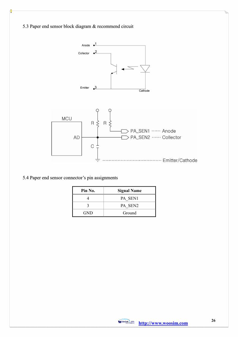
55.. PPAAPPEERR EENNDD SSEENNSSOORR A photo-sensor is used to detect the existence of the thermal paper in the path near the thermal head.
55..11 MMaaxxiimmuumm rraattiinngg ((TTaabbllee 55..11))
55..22 EElleeccttrroonn--ooppttiiccaall cchhaarraacctteerriissttiiccss ((TTaabbllee 55..22))
ITEM Symbol Rating Unit
INPUT
Power dissipation
PD 75 mW
Reverse voltage VR 5 V
Forward current IF 50 mA
Pulse forward current
IFP 1 A
OUTPUT
Collector power dissipation
PC 50 mW
Collector current IC 20 mA
C-E voltage VCEO 30 V
E-C voltage VECO 3 V
Operating temp Topr. -25 ~ +85 °C Storage temp Tstg -30 ~ +100 °C
Soldering temp Tsol. 240 °C
(Ta=25)
ITEM Symbol Conditions Min Typ Max Unit
INPUT
Forward voltage VF IF=10mA 1.3 V
Reverse current IR VR=5V 10 mA
Peak wavelength
lP 940 nm
OUTPUT Collector dark
current ICEO VCE=10V 0.2 mA
Light current IL VCE=5V, IF=10mA 90 mA
Leakage current ICEOD VEC=5V, IF=10mA 0.2 mA
Switching speeds
Rise time tr VCC=2V
IC=100mA RL=1KW
30 msec.
Fall time tf 25 msec.
(Ta=25)
http://www.woosim.com 26
55..33 PPaappeerr eenndd sseennssoorr bblloocckk ddiiaaggrraamm && rreeccoommmmeenndd cciirrccuuiitt
55..44 PPaappeerr eenndd sseennssoorr ccoonnnneeccttoorr’’ss ppiinn aassssiiggnnmmeennttss
Pin No. Signal Name
4 PA_SEN1
3 PA_SEN2
GND Ground
http://www.woosim.com 27
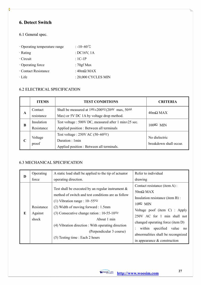
66.. DDeetteecctt SSwwiittcchh
66..11 GGeenneerraall ssppeecc.. · Operating temperature range : -10~60 · Rating : DC16V, 1A · Circuit : 1C-1P · Operating force : 70gf Max · Contact Resistance : 40mΩ MAX · Life : 20,000 CYCLES MIN
66..22 EELLEECCTTRRIICCAALL SSPPEECCIIFFIICCAATTIIOONN
66..33 MMEECCHHAANNIICCAALL SSPPEECCIIFFIICCAATTIIOONN
ITEMS TEST CONDITIONS CRITERIA
A Contact resistance
Shall be measured at 1±200(20 max, 50 Max) or 5V DC 1A by voltage drop method.
40mΩ MAX
B Insulation Resistance
Test voltage : 500V DC, measured after 1 min±25 sec. Applied position : Between all terminals
100 MIN
C Voltage proof
Test voltage : 250V AC (50~60) Duration : 1min Applied position : Between all terminals.
No dielectric breakdown shall occur.
D Operating force
A static load shall be applied to the tip of actuator operating direction.
Refer to individual drawing
E Resistance Against shock
Test shall be executed by an regular instrument & method of switch and test conditions are as follow
(1) Vibration range : 10~55 (2) Width of moving forward : 1.5mm
(3) Consecutive change ration : 10-55-10 About 1 min (4) Vibration direction : With operating direction (Perpendicular 3 course) (5) Testing time : Each 2 hours
Contact resistance (item A) : 50mΩ MAX Insulation resistance (item B) :
10 MIN Voltage poof (item C) : Apply 250V AC for 1 min shall not changed operating force (item D) : within specified value no abnormalities shall be recongnized in appearance & construction

http://www.woosim.com 28
66..44.. PPiinn SSPPEECC..
66..55.. CCiirrccuuiitt DDiiaaggrraamm && rreeccoommmmeenndd cciirrccuuiitt
Pin No. Signal Name
1 Detect Switch
2 Ground

http://www.woosim.com 29
77.. DDIIMMEENNSSIIOONNSS
The figure 8.1 illustrates the overall dimensions for the Porti-M200C thermal printing mechanism.
(Dimension in mm) ((FFiigguurree 88..11))