PIC18F6627/6722/8627/8722 Data Sheet - Datasheet-维库 ...pdf.dzsc.com/F66/PIC18F6627.pdf ·...
444
2004 Microchip Technology Inc. Advance Information DS39646A PIC18F6627/6722/8627/8722 Data Sheet 64/80-Pin 1-Mbit Enhanced Flash Microcontrollers with 10-Bit A/D and nanoWatt Technology 查询PIC18F6627供应商 查询PIC18F6627供应商
Transcript of PIC18F6627/6722/8627/8722 Data Sheet - Datasheet-维库 ...pdf.dzsc.com/F66/PIC18F6627.pdf ·...

2004 Microchip Technology Inc. Advance Information DS39646A
PIC18F6627/6722/8627/8722Data Sheet
64/80-Pin1-Mbit Enhanced Flash Microcontrollers
with 10-Bit A/D and nanoWatt Technology
查询PIC18F6627供应商查询PIC18F6627供应商

DS39646A-page ii Advance Information 2004 Microchip Technology Inc.
Information contained in this publication regarding deviceapplications and the like is provided only for your convenienceand may be superseded by updates. It is your responsibility toensure that your application meets with your specifications.MICROCHIP MAKES NO REPRESENTATIONS OR WAR-RANTIES OF ANY KIND WHETHER EXPRESS OR IMPLIED,WRITTEN OR ORAL, STATUTORY OR OTHERWISE,RELATED TO THE INFORMATION, INCLUDING BUT NOTLIMITED TO ITS CONDITION, QUALITY, PERFORMANCE,MERCHANTABILITY OR FITNESS FOR PURPOSE.Microchip disclaims all liability arising from this information andits use. Use of Microchip’s products as critical components inlife support systems is not authorized except with expresswritten approval by Microchip. No licenses are conveyed,implicitly or otherwise, under any Microchip intellectual propertyrights.
Trademarks
The Microchip name and logo, the Microchip logo, Accuron, dsPIC, KEELOQ, microID, MPLAB, PIC, PICmicro, PICSTART, PRO MATE, PowerSmart, rfPIC, and SmartShunt are registered trademarks of Microchip Technology Incorporated in the U.S.A. and other countries.
AmpLab, FilterLab, MXDEV, MXLAB, PICMASTER, SEEVAL, SmartSensor and The Embedded Control Solutions Company are registered trademarks of Microchip Technology Incorporated in the U.S.A.
Analog-for-the-Digital Age, Application Maestro, dsPICDEM, dsPICDEM.net, dsPICworks, ECAN, ECONOMONITOR, FanSense, FlexROM, fuzzyLAB, In-Circuit Serial Programming, ICSP, ICEPIC, Migratable Memory, MPASM, MPLIB, MPLINK, MPSIM, PICkit, PICDEM, PICDEM.net, PICLAB, PICtail, PowerCal, PowerInfo, PowerMate, PowerTool, rfLAB, rfPICDEM, Select Mode, Smart Serial, SmartTel and Total Endurance are trademarks of Microchip Technology Incorporated in the U.S.A. and other countries.
SQTP is a service mark of Microchip Technology Incorporated in the U.S.A.
All other trademarks mentioned herein are property of their respective companies.
© 2004, Microchip Technology Incorporated, Printed in the U.S.A., All Rights Reserved.
Printed on recycled paper.
Note the following details of the code protection feature on Microchip devices:
• Microchip products meet the specification contained in their particular Microchip Data Sheet.
• Microchip believes that its family of products is one of the most secure families of its kind on the market today, when used in the intended manner and under normal conditions.
• There are dishonest and possibly illegal methods used to breach the code protection feature. All of these methods, to our knowledge, require using the Microchip products in a manner outside the operating specifications contained in Microchip’s Data Sheets. Most likely, the person doing so is engaged in theft of intellectual property.
• Microchip is willing to work with the customer who is concerned about the integrity of their code.
• Neither Microchip nor any other semiconductor manufacturer can guarantee the security of their code. Code protection does not mean that we are guaranteeing the product as “unbreakable.”
Code protection is constantly evolving. We at Microchip are committed to continuously improving the code protection features of ourproducts. Attempts to break Microchip’s code protection feature may be a violation of the Digital Millennium Copyright Act. If such actsallow unauthorized access to your software or other copyrighted work, you may have a right to sue for relief under that Act.
Microchip received ISO/TS-16949:2002 quality system certification for its worldwide headquarters, design and wafer fabrication facilities in Chandler and Tempe, Arizona and Mountain View, California in October 2003. The Company’s quality system processes and procedures are for its PICmicro® 8-bit MCUs, KEELOQ® code hopping devices, Serial EEPROMs, microperipherals, nonvolatile memory and analog products. In addition, Microchip’s quality system for the design and manufacture of development systems is ISO 9001:2000 certified.

2004 Microchip Technology Inc. Advance Information DS39646A-page 1
PIC18F6627/6722/8627/8722
Power-Managed Modes:• Run: CPU on, peripherals on• Idle: CPU off, peripherals on• Sleep: CPU off, peripherals off• Idle mode currents down to 15 µA typical• Sleep current down to 0.2 µA typical• Timer1 Oscillator: 1.8 µA, 32 kHz, 2V• Watchdog Timer: 2.1 µA• Two-Speed Oscillator Start-up
Flexible Oscillator Structure:• Four Crystal modes, up to 25 MHz• 4X Phase Lock Loop (PLL) (available for crystal and
internal oscillators)• Two External RC modes, up to 4 MHz• Two External Clock modes, up to 40 MHz• Internal oscillator block:
- 8 user selectable frequencies, from 31 kHz to 8 MHz- Provides a complete range of clock speeds from
31 kHz to 32 MHz when used with PLL- User tunable to compensate for frequency drift
• Secondary oscillator using Timer1 @ 32 kHz• Fail-Safe Clock Monitor:
- Allows for safe shutdown if peripheral clock stops
External Memory Interface (PIC18F8627/8722 only):• Address capability of up to 2 Mbytes• 8-bit or 16-bit interface
Peripheral Highlights:• High current sink/source 25 mA/25 mA• Four programmable external interrupts• Four input change interrupts• Two Capture/Compare/PWM (CCP) modules
Peripheral Highlights (Continued):• Three Enhanced Capture/Compare/PWM (ECCP)
modules:- One, two or four PWM outputs- Selectable polarity- Programmable dead-time- Auto-Shutdown and Auto-Restart
• Two Master Synchronous Serial Port (MSSP) modules supporting 2/3/4-wire SPI™ (all 4 modes) and I2C™ Master and Slave modes
• Two Enhanced Addressable USART modules:- Supports RS-485, RS-232 and LIN 1.2- RS-232 operation using internal oscillator block
(no external crystal required)- Auto-wake-up on Start bit- Auto-baud detect
• 10-bit, up to 16-channel Analog-to-Digital Converter module (A/D) - Auto-acquisition capability- Conversion available during Sleep
• Dual analog comparators with input multiplexing
Special Microcontroller Features:• C compiler optimized architecture:
- Optional extended instruction set designed to optimize re-entrant code
• 100,000 erase/write cycle Enhanced Flash program memory typical
• 1,000,000 erase/write cycle Data EEPROM memory typical
• Flash/Data EEPROM Retention: 100 years typical• Self-programmable under software control• Priority levels for interrupts• 8 X 8 Single Cycle Hardware Multiplier• Extended Watchdog Timer (WDT):
- Programmable period from 4 ms to 131s• Single-supply In-Circuit Serial Programming™
(ICSP™) via two pins• In-Circuit Debug (ICD) via two pins• Wide operating voltage range: 2.0V to 5.5V
Device
Program Memory Data Memory
I/O10-bit
A/D (ch)
CCP/ECCP(PWM)
MSSP
EU
SA
RT
Com
para
tors
Tim
ers
8/16
-bit
Ext
erna
l Bus
Flash(bytes)
# Single-Word
Instructions
SRAM(bytes)
EEPROM(bytes)
SPI™MasterI2C™
PIC18F6627 96 K 49152 3936 1024 54 12 2/3 2 Y Y 2 2 2/3 N
PIC18F6722 128 K 65536 3936 1024 54 12 2/3 2 Y Y 2 2 2/3 N
PIC18F8627 96 K 49152 3936 1024 70 16 2/3 2 Y Y 2 2 2/3 Y
PIC18F8722 128 K 65536 3936 1024 70 16 2/3 2 Y Y 2 2 2/3 Y
64/80-Pin 1-Mbit Enhanced Flash Microcontrollers with10-Bit A/D and nanoWatt Technology

PIC18F6627/6722/8627/8722
DS39646A-page 2 Advance Information 2004 Microchip Technology Inc.
Pin Diagrams
Note 1: The CCP2/P2A pin placement is determined by the CCP2MX configuration bit and Processor mode settings.
PIC18F6627
1
2
3
4
5
6
7
8
9
10
11
12
13
14
38
37
36
35
34
33
50 49
17 18 19 20 21 22 23 24 25 26
RE
2/C
S/P
2B
RE
3/P
3C
RE
4/P
3B
RE
5/P
1C
RE
6/P
1B
RE
7/C
CP
2(1) /P
2A(1
)
RD
0/P
SP
0
VD
D
VS
S
RD
1/P
SP
1
RD
2/P
SP
2
RD
3/P
SP
3
RD
4/P
SP
4/S
DO
2
RD
5/P
SP
5/S
DI2
/SD
A2
RD
6/P
SP
6/S
CK
2/S
CL2
RD
7/P
SP
7/S
S2
RE1/WR/P2C
RE0/RD/P2D
RG0/CCP3/P3A
RG1/TX2/CK2
RG2/RX2/DT2
RG3/CCP4/P3D
RG5/MCLR/VPP
RG4/CCP5/P1D
VSS
VDD
RF7/SS1RF6/AN11
RF5/AN10/CVREF
RF4/AN9
RF3/AN8
RF2/AN7/C1OUT
RB0/INT0/FLT0
RB1/INT1
RB2/INT2
RB3/INT3
RB4/KBI0
RB5/KBI1/PGM
RB6/KBI2/PGC
VSS
RA6/OSC2/CLKO
RA7/OSC1/CLKI
VDD
RB7/KBI3/PGD
RC4/SDI1/SDA1
RC3/SCK1/SCL1
RC2/CCP1/P1A
RF
0/A
N5
RF
1/A
N6/
C2O
UT
AV
DD
AV
SS
RA
3/A
N3/
VR
EF+
RA
2/A
N2/
VR
EF-
RA
1/A
N1
RA
0/A
N0
VS
S
VD
D
RA
4/T
0CK
I
RA
5/A
N4/
HLV
DIN
RC
1/T
1OS
I/CC
P2(1
) /P2A
(1)
RC
0/T
1OS
O/T
13C
KI
RC
7/R
X1/
DT
1
RC
6/T
X1/
CK
1
RC5/SDO1
15
16
31
40
39
27 28 29 30 32
48
47
46
45
44
43
42
41
54 53 52 5158 57 56 5560 5964 63 62 61
64-Pin TQFP
PIC18F6722

2004 Microchip Technology Inc. Advance Information DS39646A-page 3
PIC18F6627/6722/8627/8722
Pin Diagrams (Continued)
PIC18F8627
345678910111213141516
48474645
44434241
4039
64 63 62 61
21 22 23 24 25 26 27 28 29 30 31 32
RE
2/A
D10
/CS
/P2B
RE
3/A
D11
/P3C
(2)
RE
4/A
D12
/P3B
(2)
RE
5/A
D13
/P1C
(2)
RE
6/A
D14
/P1B
(2)
RE
7/A
D15
/CC
P2(1
) /P2A
(1)
RD
0/A
D0/
PS
P0
VD
D
VS
S
RD
1/A
D1/
PS
P1
RD
2/A
D2/
PS
P2
RD
3/A
D3/
PS
P3
RD
4/A
D4/
PS
P4/
SD
O2
RD
5/A
D5/
PS
P5/
SD
I2/S
DA
2
RD
6/A
D6/
PS
P6/
SC
K2/
SC
L2R
D7/
AD
7/P
SP
7/S
S2
RE1/AD9/WR/P2CRE0/AD8/RD/P2D
RG0/CCP3/P3ARG1/TX2/CK2RG2/RX2/DT2
RG3/CCP4/P3DRG5/MCLR/VPP
RG4/CCP5/P1DVSS
VDD
RF7/SS1
RB0/INT0/FLT0RB1/INT1
RB2/INT2RB3/INT3/CCP2(1)/P2A(1)
RB4/KBI0RB5/KBI1/PGMRB6/KBI2/PGCVSS
RA6/OSC2/CLKORA7/OSC1/CLKIVDD
RB7/KBI3/PGD
RC4/SDI1/SDA1RC3/SCK1/SCL1RC2/CCP1/P1A
RF
0/A
N5
RF
1/A
N6/
C2O
UT
AV
DD
AV
SS
RA
3/A
N3/
VR
EF+
RA
2/A
N2/
VR
EF-
RA
1/A
N1
RA
0/A
N0
VS
S
VD
D
RA
4/T
0CK
I
RA
5/A
N4/
HLV
DIN
RC
1/T
1OS
I/CC
P2(1
) /P2A
(1)
RC
0/T
1OS
O/T
13C
KI
RC
7/R
X1/
DT
1R
C6/
TX
1/C
K1
RC5/SDO1
RJ0
/ALE
RJ1
/OE
RH
1/A
17
RH
0/A
16
12
RH2/A18RH3/A19
1718
RH7/AN15/P1B(2)
RH6/AN14/P1C(2)
RH
5/A
N13
/P3B
(2)
RH
4/A
N12
/P3C
(2)
RJ5
/CE
RJ4
/BA
0
37
RJ7/UBRJ6/LB
5049
RJ2/WRLRJ3/WRH
1920
33 34 35 36 38
58575655
54535251
6059
68 67 66 6572 71 70 6974 7378 77 76 757980
80-Pin TQFP
Note 1: The CCP2/P2A pin placement is determined by the CCP2MX configuration bit and Processor mode settings.2: P1B, P1C, P3B and P3C pin placement is determined by the ECCPMX configuration bit.
RF5/AN10/CVREF
RF4/AN9RF3/AN8
RF2/AN7/C1OUT
RF6/AN11
PIC18F8722

PIC18F6627/6722/8627/8722
DS39646A-page 4 Advance Information 2004 Microchip Technology Inc.
Table of Contents
1.0 Device Overview .......................................................................................................................................................................... 72.0 Oscillator Configurations ............................................................................................................................................................ 313.0 Power-Managed Modes ............................................................................................................................................................. 414.0 Reset .......................................................................................................................................................................................... 495.0 Memory Organization ................................................................................................................................................................. 636.0 Flash Program Memory.............................................................................................................................................................. 857.0 External Memory Bus ................................................................................................................................................................. 958.0 Data EEPROM Memory ........................................................................................................................................................... 1099.0 8 x 8 Hardware Multiplier.......................................................................................................................................................... 11510.0 Interrupts .................................................................................................................................................................................. 11711.0 I/O Ports ................................................................................................................................................................................... 13312.0 Timer0 Module ......................................................................................................................................................................... 16113.0 Timer1 Module ......................................................................................................................................................................... 16514.0 Timer2 Module ......................................................................................................................................................................... 17115.0 Timer3 Module ......................................................................................................................................................................... 17316.0 Timer4 Module ......................................................................................................................................................................... 17717.0 Capture/Compare/PWM (CCP) Modules ................................................................................................................................. 17918.0 Enhanced Capture/Compare/PWM (ECCP) Module................................................................................................................ 18719.0 Master Synchronous Serial Port (MSSP) Module .................................................................................................................... 20520.0 Enhanced Universal Synchronous Receiver Transmitter (EUSART) ....................................................................................... 24721.0 10-Bit Analog-to-Digital Converter (A/D) Module ..................................................................................................................... 26922.0 Comparator Module.................................................................................................................................................................. 27923.0 Comparator Voltage Reference Module................................................................................................................................... 28524.0 High/Low-Voltage Detect (HLVD)............................................................................................................................................. 28925.0 Special Features of the CPU.................................................................................................................................................... 29526.0 Instruction Set Summary .......................................................................................................................................................... 31727.0 Development Support............................................................................................................................................................... 36728.0 Electrical Characteristics .......................................................................................................................................................... 37329.0 DC and AC Characteristics Graphs and Tables....................................................................................................................... 41730.0 Packaging Information.............................................................................................................................................................. 419Appendix A: Revision History............................................................................................................................................................. 423Appendix B: Device Differences......................................................................................................................................................... 423Appendix C: Conversion Considerations ........................................................................................................................................... 424Appendix D: Migration from Baseline to Enhanced Devices.............................................................................................................. 424Appendix E: Migration from Mid-Range to Enhanced Devices .......................................................................................................... 425Appendix F: Migration from High-End to Enhanced Devices ............................................................................................................. 425On-Line Support................................................................................................................................................................................. 439Systems Information and Upgrade Hot Line ...................................................................................................................................... 439Reader Response .............................................................................................................................................................................. 440PIC18F6627/6722/8627/8722 Product Identification System ............................................................................................................ 441

2004 Microchip Technology Inc. Advance Information DS39646A-page 5
PIC18F6627/6722/8627/8722
TO OUR VALUED CUSTOMERS
It is our intention to provide our valued customers with the best documentation possible to ensure successful use of your Microchipproducts. To this end, we will continue to improve our publications to better suit your needs. Our publications will be refined andenhanced as new volumes and updates are introduced.
If you have any questions or comments regarding this publication, please contact the Marketing Communications Department viaE-mail at [email protected] or fax the Reader Response Form in the back of this data sheet to (480) 792-4150. Wewelcome your feedback.
Most Current Data SheetTo obtain the most up-to-date version of this data sheet, please register at our Worldwide Web site at:
http://www.microchip.com
You can determine the version of a data sheet by examining its literature number found on the bottom outside corner of any page.The last character of the literature number is the version number, (e.g., DS30000A is version A of document DS30000).
ErrataAn errata sheet, describing minor operational differences from the data sheet and recommended workarounds, may exist for currentdevices. As device/documentation issues become known to us, we will publish an errata sheet. The errata will specify the revisionof silicon and revision of document to which it applies.
To determine if an errata sheet exists for a particular device, please check with one of the following:
• Microchip’s Worldwide Web site; http://www.microchip.com• Your local Microchip sales office (see last page)When contacting a sales office, please specify which device, revision of silicon and data sheet (include literature number) you areusing.
Customer Notification SystemRegister on our web site at www.microchip.com to receive the most current information on all of our products.

PIC18F6627/6722/8627/8722
DS39646A-page 6 Advance Information 2004 Microchip Technology Inc.
NOTES:

2004 Microchip Technology Inc. Advance Information DS39646A-page 7
PIC18F6627/6722/8627/8722
1.0 DEVICE OVERVIEW
This document contains device specific information forthe following devices:
This family offers the advantages of all PIC18 micro-controllers – namely, high computational performanceat an economical price – with the addition of high-endurance, Enhanced Flash program memory. On topof these features, the PIC18F6627/6722/8627/8722family introduces design enhancements that makethese microcontrollers a logical choice for many high-performance, power sensitive applications.
1.1 New Core Features
1.1.1 nanoWatt TECHNOLOGY
All of the devices in the PIC18F6627/6722/8627/8722family incorporate a range of features that can signifi-cantly reduce power consumption during operation.Key items include:
• Alternate Run Modes: By clocking the controller from the Timer1 source or the internal oscillator block, power consumption during code execution can be significantly reduced.
• Multiple Idle Modes: The controller can also run with its CPU core disabled but the peripherals still active. In these states, power consumption can be reduced even further.
• On-the-fly Mode Switching: The power-managed modes are invoked by user code during operation, allowing the user to incorporate power-saving ideas into their application’s software design.
• Low Consumption in Key Modules: The power requirements for both Timer1 and the Watchdog Timer are minimized. See Section 28.0 “Electrical Characteristics” for values.
1.1.2 EXPANDED MEMORY
The PIC18F6627/6722/8627/8722 family providesample room for application code, and includesmembers with 96 Kbytes or 128 Kbytes of code space.
• Data RAM and Data EEPROM: The PIC18F6627/6722/8627/8722 family also provides plenty of roomfor application data. The devices have 3936 bytes ofdata RAM, as well as 1024 bytes of data EEPROMfor long term retention of non-volatile data.
• Memory Endurance: The Enhanced Flash cells for both program memory and data EEPROM are rated to last for many thousands of erase/write cycles – up to 100,000 for program memory and 1,000,000 for EEPROM. Data retention without refresh is conservatively estimated to be greater than 40 years.
1.1.3 MULTIPLE OSCILLATOR OPTIONS AND FEATURES
All of the devices in the PIC18F6627/6722/8627/8722family offer ten different oscillator options, allowingusers a wide range of choices in developing applicationhardware. These include:
• Four Crystal modes, using crystals or ceramic resonators
• Two External Clock modes, offering the option of using two pins (oscillator input and a divide-by-4 clock output) or one pin (oscillator input, with the second pin reassigned as general I/O)
• Two External RC Oscillator modes with the same pin options as the External Clock modes
• An internal oscillator block which provides an 8 MHz clock and an INTRC source (approxi-mately 31 kHz), as well as a range of 6 user selectable clock frequencies, between 125 kHz to 4 MHz, for a total of 8 clock frequencies. This option frees the two oscillator pins for use as additional general purpose I/O.
• A Phase Lock Loop (PLL) frequency multiplier, available to both the high-speed crystal and inter-nal oscillator modes, which allows clock speeds of up to 40 MHz. Used with the internal oscillator, the PLL gives users a complete selection of clock speeds, from 31 kHz to 32 MHz – all without using an external crystal or clock circuit.
Besides its availability as a clock source, the internaloscillator block provides a stable reference source thatgives the family additional features for robustoperation:
• Fail-Safe Clock Monitor: This option constantly monitors the main clock source against a refer-ence signal provided by the internal oscillator. If a clock failure occurs, the controller is switched to the internal oscillator block, allowing for continued low-speed operation or a safe application shutdown.
• Two-Speed Start-up: This option allows the internal oscillator to serve as the clock source from Power-on Reset, or wake-up from Sleep mode, until the primary clock source is available.
• PIC18F6627 • PIC18LF6627
• PIC18F6722 • PIC18LF6722
• PIC18F8627 • PIC18LF8627
• PIC18F8722 • PIC18LF8722
PIC18F6627/6722/8627/8722
DS39646A-page 8 Advance Information 2004 Microchip Technology Inc.
1.1.4 EXTERNAL MEMORY INTERFACE
In the unlikely event that 128 Kbytes of programmemory is inadequate for an application, thePIC18F8627/8722 members of the family alsoimplement an external memory interface. This allowsthe controller’s internal program counter to address amemory space of up to 2 MBytes, permitting a level ofdata access that few 8-bit devices can claim.
With the addition of new operating modes, the externalmemory interface offers many new options, including:
• Operating the microcontroller entirely from externalmemory
• Using combinations of on-chip and externalmemory, up to the 2-Mbyte limit
• Using external Flash memory for reprogrammable application code or large data tables
• Using external RAM devices for storing large amounts of variable data
1.1.5 EASY MIGRATION
Regardless of the memory size, all devices share thesame rich set of peripherals, allowing for a smoothmigration path as applications grow and evolve.
The consistent pinout scheme used throughout theentire family also aids in migrating to the next largerdevice. This is true when moving between the 64-pinmembers, between the 80-pin members, or even jump-ing from 64-pin to 80-pin devices.
1.2 Other Special Features
• Communications: The PIC18F6627/6722/8627/8722 family incorporates a range of serial communi-cation peripherals, including 2 independentenhanced USARTs and 2 Master SSP modulescapable of both SPI and I2C (Master and Slave)modes of operation. Also, for PIC18F6627/6722/8627/8722 devices, one of the general purpose I/Oports can be reconfigured as an 8-bit parallel slaveport for direct processor-to-processor communica-tions.
• CCP Modules: All devices in the family incorporatetwo Capture/Compare/PWM (CCP) modules andthree enhanced CCP modules to maximize flexibilityin control applications. Up to four different timebases may be used to perform several differentoperations at once. Each of the three ECCPs offerup to four PWM outputs, allowing for a total of 12PWMs. The ECCPs also offer many beneficialfeatures, including polarity selection, ProgrammableDead-Time, Auto-Shutdown and Restart, and Half-Bridge and Full-Bridge Output modes.
• Self-programmability: These devices can write to their own program memory spaces under inter-nal software control. By using a bootloader routine located in the protected Boot Block at the top of program memory, it becomes possible to create an application that can update itself in the field.
• Extended Instruction Set: The PIC18F6627/6722/8627/8722 family introduces an optional extension to the PIC18 instruction set, which adds 8 new instructions and an Indexed Addressing mode. This extension, enabled as a device con-figuration option, has been specifically designed to optimize re-entrant application code originally developed in high-level languages, such as C.
• 10-bit A/D Converter: This module incorporates programmable acquisition time, allowing for a channel to be selected and a conversion to be initiated without waiting for a sampling period and thus, reduce code overhead.
• Extended Watchdog Timer (WDT): This enhanced version incorporates a 16-bit prescaler, allowing an extended time-out range that is stable across operating voltage and temperature. See Section 28.0 “Electrical Characteristics” for time-out periods.
1.3 Details on Individual Family Members
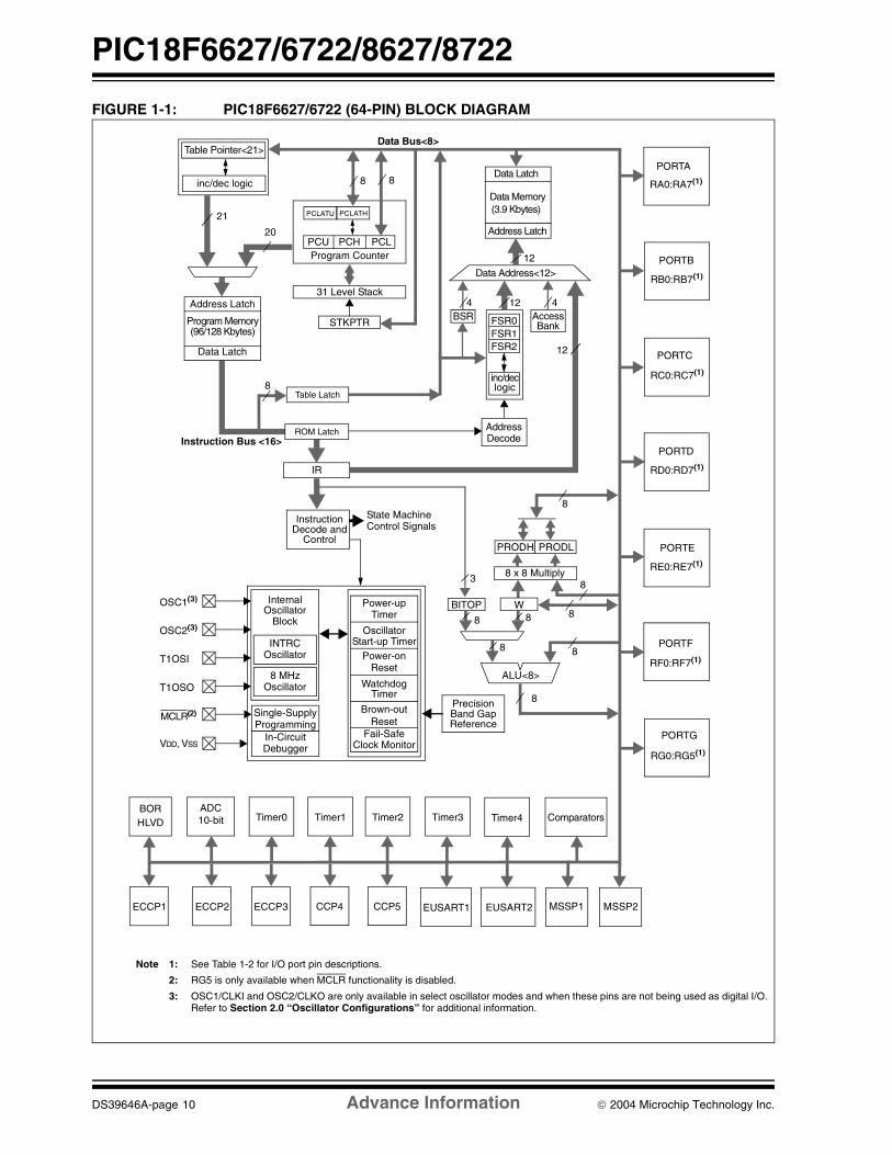
Devices in the PIC18F6627/6722/8627/8722 family areavailable in 64-pin and 80-pin packages. Blockdiagrams for the two groups are shown in Figure 1-1and Figure 1-2.
The devices are differentiated from each other in fiveways:
1. Flash program memory (96 Kbytes forPIC18F6627/8627 devices and 128 Kbytes forPIC18F6722/8722).
2. A/D channels (12 for 64-pin devices, 16 for80-pin devices).
3. I/O ports (7 bidirectional ports on 64-pin devices,9 bidirectional ports on 80-pin devices).
4. External Memory Bus, configurable for 8 and16-bit operation, is available on PIC18F8627/8722 devices.
All other features for devices in this family are identical.These are summarized in Table 1-1.
The pinouts for all devices are listed in Table 1-2 andTable 1-3.
Like all Microchip PIC18 devices, members of thePIC18F6627/6722/8627/8722 family are available asboth standard and low-voltage devices. Standarddevices with Enhanced Flash memory, designated withan “F” in the part number (such as PIC18F6627),accommodate an operating VDD range of 4.2V to 5.5V.Low-voltage parts, designated by “LF” (such asPIC18LF6627), function over an extended VDD rangeof 2.0V to 5.5V.

2004 Microchip Technology Inc. Advance Information DS39646A-page 9
PIC18F6627/6722/8627/8722
TABLE 1-1: DEVICE FEATURES
Features PIC18F6627 PIC18F6722 PIC18F8627 PIC18F8722
Operating Frequency DC – 40 MHz DC – 40 MHz DC – 40 MHz DC – 40 MHz
Program Memory (Bytes) 96K 128K 96K 128K
Program Memory (Instructions)
49152 65536 49152 65536
Data Memory (Bytes) 3936 3936 3936 3936
Data EEPROM Memory (Bytes) 1024 1024 1024 1024
Interrupt Sources 28 28 29 29
I/O Ports Ports A, B, C, D, E, F, G Ports A, B, C, D, E, F, G Ports A, B, C, D, E, F, G, H, J
Ports A, B, C, D, E, F, G, H, J
Timers 5 5 5 5
Capture/Compare/PWM Modules 2 2 2 2
Enhanced Capture/Compare/PWM Modules
3 3 3 3
Enhanced USART 2 2 2 2
Serial Communications MSSP, Enhanced USART
MSSP, Enhanced USART
MSSP, Enhanced USART
MSSP, Enhanced USART
Parallel Communications (PSP) Yes Yes Yes Yes
10-bit Analog-to-Digital Module 12 Input Channels 12 Input Channels 16 Input Channels 16 Input Channels
Resets (and Delays) POR, BOR, RESET Instruction, Stack Full, Stack
Underflow (PWRT, OST), MCLR (optional), WDT
POR, BOR, RESET Instruction, Stack Full, Stack
Underflow (PWRT, OST), MCLR (optional), WDT
POR, BOR, RESET Instruction, Stack Full, Stack
Underflow (PWRT, OST), MCLR (optional), WDT
POR, BOR, RESET Instruction, Stack Full, Stack
Underflow (PWRT, OST), MCLR (optional), WDT
Programmable High/Low-Voltage Detect
Yes Yes Yes Yes
Programmable Brown-out Reset Yes Yes Yes Yes
Instruction Set 75 Instructions; 83 with Extended
Instruction Set enabled
75 Instructions; 83 with Extended
Instruction Set enabled
75 Instructions; 83 with Extended
Instruction Set enabled
75 Instructions; 83 with Extended
Instruction Set enabled
Packages 64-pin TQFP 64-pin TQFP 80-pin TQFP 80-pin TQFP
PIC18F6627/6722/8627/8722
DS39646A-page 10 Advance Information 2004 Microchip Technology Inc.
FIGURE 1-1: PIC18F6627/6722 (64-PIN) BLOCK DIAGRAM
InstructionDecode and
Control
PORTAData Latch
Data Memory(3.9 Kbytes)
Address Latch
Data Address<12>
12
AccessBSR FSR0FSR1FSR2
inc/declogic
Address
4 12 4
PCH PCL
PCLATH
8
31 Level Stack
Program Counter
PRODLPRODH
8 x 8 Multiply
8
BITOP88
ALU<8>
Address Latch
Program Memory(96/128 Kbytes)
Data Latch
20
8
8
Table Pointer<21>
inc/dec logic
21
8
Data Bus<8>
Table Latch8
IR
12
3
PCLATU
PCU
Note 1: See Table 1-2 for I/O port pin descriptions.
2: RG5 is only available when MCLR functionality is disabled.
3: OSC1/CLKI and OSC2/CLKO are only available in select oscillator modes and when these pins are not being used as digital I/O.Refer to Section 2.0 “Oscillator Configurations” for additional information.
EUSART1
Comparators
MSSP1
Timer2Timer1 Timer3Timer0HLVD
ECCP1
BOR ADC10-bit
W
Instruction Bus <16>
STKPTR Bank
8
State MachineControl Signals
Decode
8
8
Power-upTimer
OscillatorStart-up Timer
Power-onReset
WatchdogTimer
OSC1(3)
OSC2(3)
VDD,
Brown-outReset
InternalOscillator
Fail-SafeClock Monitor
Precision
ReferenceBand Gap
VSS
MCLR(2)
Block
INTRCOscillator
8 MHzOscillator
Single-SupplyProgramming
In-CircuitDebugger
T1OSI
T1OSO
EUSART2ECCP2
ROM Latch
ECCP3 MSSP2CCP4 CCP5
PORTC
PORTD
PORTE
PORTF
PORTG
RA0:RA7(1)
RC0:RC7(1)
RD0:RD7(1)
RE0:RE7(1)
RF0:RF7(1)
RG0:RG5(1)
PORTB
RB0:RB7(1)
Timer4

2004 Microchip Technology Inc. Advance Information DS39646A-page 11
PIC18F6627/6722/8627/8722FIGURE 1-2: PIC18F8627/8722 (80-PIN) BLOCK DIAGRAM
PRODLPRODH
8 x 8 Multiply
8
BITOP88
ALU<8>
8
83
W8
8
8Power-up
Timer
OscillatorStart-up Timer
Power-onReset
WatchdogTimer
OSC1(3)
OSC2(3)
VDD,
Brown-outReset
InternalOscillator
Fail-SafeClock Monitor
Precision
ReferenceBand Gap
VSS
MCLR(2)
Block
INTRCOscillator
8 MHzOscillator
Single-SupplyProgramming
In-CircuitDebugger
T1OSI
T1OSO
InstructionDecode &
Control
Data Latch
Data Memory(3.9 Kbytes)
Address Latch
Data Address<12>
12
AccessBSR FSR0FSR1FSR2
inc/declogic
Address
4 12 4
PCH PCL
PCLATH
8
31 Level Stack
Program Counter
Address Latch
Program Memory(96/128 Kbytes)
Data Latch
20
Table Pointer<21>
inc/dec logic
21
8
Data Bus<8>
TABLE LATCH
8
IR
12
ROM LATCH
PCLATU
PCU
Instruction Bus <16>
STKPTR Bank
State MachineControl Signals
Decode
Sys
tem
Bus
Inte
rfac
e
AD15:AD0, A19:A16(Multiplexed with PORTD,PORTE and PORTH)
PORTA
PORTC
PORTD
PORTE
PORTF
PORTG
RA0:RA7(1)
RC0:RC7(1)
RD0:RD7(1)
RE0:RE7(1)
RF0:RF7(1)
RG0:RG5(1)
PORTB
RB0:RB7(1)
PORTH
RH0:RH7(1)
PORTJ
RJ0:RJ7(1)
EUSART1
Comparators
MSSP1
Timer2Timer1 Timer3Timer0HLVD
ECCP1
BOR ADC10-bit
EUSART2ECCP2 ECCP3 MSSP2CCP4 CCP5
Timer4
Note 1: See Table 1-3 for I/O port pin descriptions.
2: RG5 is only available when MCLR functionality is disabled.
3: OSC1/CLKI and OSC2/CLKO are only available in select oscillator modes and when these pins are not being used as digital I/O.Refer to Section 2.0 “Oscillator Configurations” for additional information.

PIC18F6627/6722/8627/8722
DS39646A-page 12 Advance Information 2004 Microchip Technology Inc.
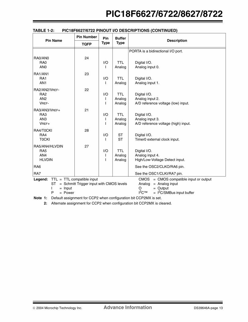
TABLE 1-2: PIC18F6627/6722 PINOUT I/O DESCRIPTIONS
Pin NamePin Number Pin
TypeBufferType
DescriptionTQFP
RG5/MCLR/VPP
RG5MCLR
VPP
7II
P
STST
Master Clear (input) or programming voltage (input).Digital input.Master Clear (Reset) input. This pin is an active-low Reset to the device.Programming voltage input.
OSC1/CLKI/RA7OSC1
CLKI
RA7
39I
I
I/O
ST
CMOS
TTL
Oscillator crystal or external clock input.Oscillator crystal input or external clock source input. ST buffer when configured in RC mode, CMOS otherwise.External clock source input. Always associated with pin function OSC1. (See related OSC1/CLKI, OSC2/CLKO pins.)General purpose I/O pin.
OSC2/CLKO/RA6OSC2
CLKO
RA6
40O
O
I/O
—
—
TTL
Oscillator crystal or clock output.Oscillator crystal output. Connects to crystal or resonator in Crystal Oscillator mode.In RC mode, OSC2 pin outputs CLKO, which has 1/4 the frequency of OSC1 and denotes the instruction cycle rate. General purpose I/O pin.
Legend: TTL = TTL compatible input CMOS = CMOS compatible input or output ST = Schmitt Trigger input with CMOS levels Analog = Analog input I = Input O = Output P = Power I2C™ = I2C/SMBus input buffer
Note 1: Default assignment for CCP2 when configuration bit CCP2MX is set.2: Alternate assignment for CCP2 when configuration bit CCP2MX is cleared.
2004 Microchip Technology Inc. Advance Information DS39646A-page 13
PIC18F6627/6722/8627/8722
PORTA is a bidirectional I/O port.
RA0/AN0RA0AN0
24I/OI
TTLAnalog
Digital I/O.Analog input 0.
RA1/AN1RA1AN1
23I/OI
TTLAnalog
Digital I/O.Analog input 1.
RA2/AN2/VREF-RA2AN2VREF-
22I/OII
TTLAnalogAnalog
Digital I/O.Analog input 2.A/D reference voltage (low) input.
RA3/AN3/VREF+RA3AN3VREF+
21I/OII
TTLAnalogAnalog
Digital I/O.Analog input 3.A/D reference voltage (high) input.
RA4/T0CKIRA4T0CKI
28I/OI
STST
Digital I/O.Timer0 external clock input.
RA5/AN4/HLVDINRA5AN4HLVDIN
27I/OII
TTLAnalogAnalog
Digital I/O.Analog input 4. High/Low-Voltage Detect input.
RA6 See the OSC2/CLKO/RA6 pin.
RA7 See the OSC1/CLKI/RA7 pin.
TABLE 1-2: PIC18F6627/6722 PINOUT I/O DESCRIPTIONS (CONTINUED)
Pin NamePin Number Pin
TypeBufferType
DescriptionTQFP
Legend: TTL = TTL compatible input CMOS = CMOS compatible input or output ST = Schmitt Trigger input with CMOS levels Analog = Analog input I = Input O = Output P = Power I2C™ = I2C/SMBus input buffer
Note 1: Default assignment for CCP2 when configuration bit CCP2MX is set.
2: Alternate assignment for CCP2 when configuration bit CCP2MX is cleared.
PIC18F6627/6722/8627/8722
DS39646A-page 14 Advance Information 2004 Microchip Technology Inc.
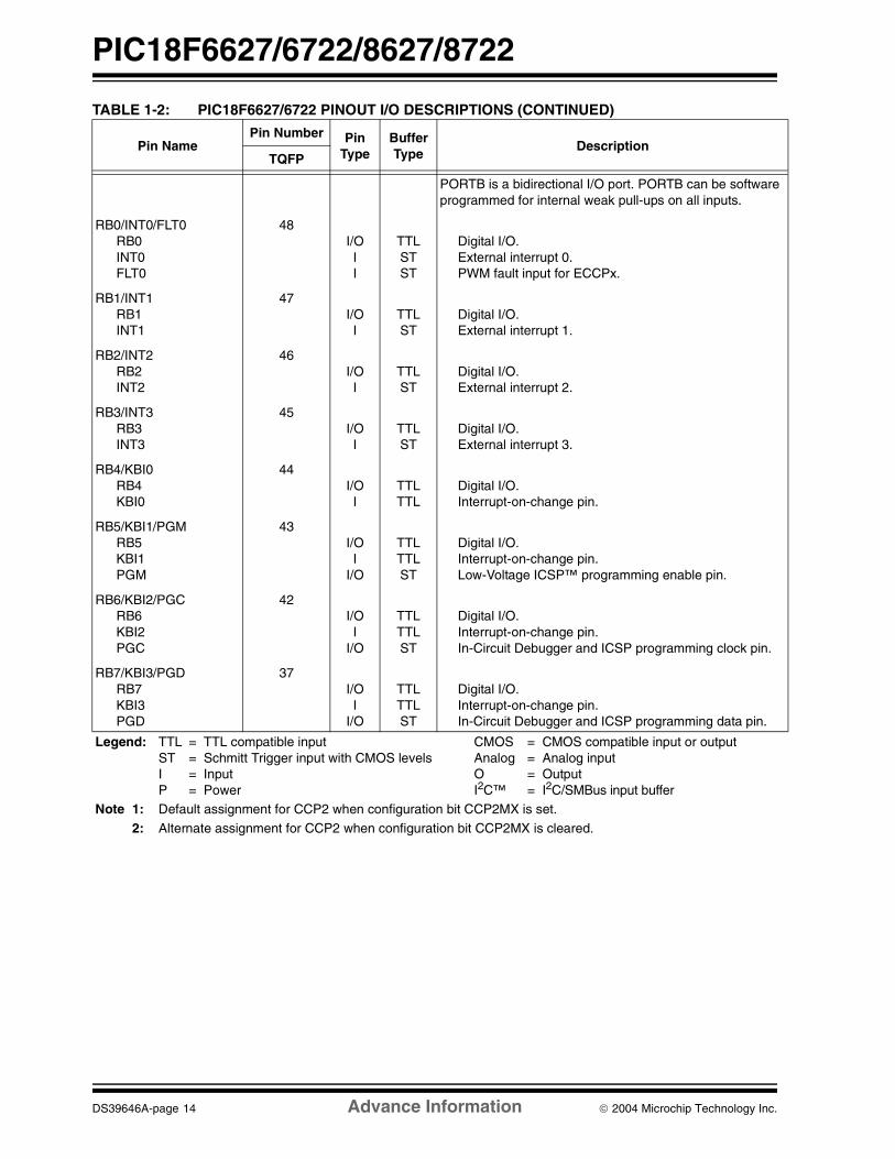
PORTB is a bidirectional I/O port. PORTB can be software programmed for internal weak pull-ups on all inputs.
RB0/INT0/FLT0RB0INT0FLT0
48I/OII
TTLSTST
Digital I/O.External interrupt 0.PWM fault input for ECCPx.
RB1/INT1RB1INT1
47I/OI
TTLST
Digital I/O.External interrupt 1.
RB2/INT2RB2INT2
46I/OI
TTLST
Digital I/O.External interrupt 2.
RB3/INT3RB3INT3
45I/OI
TTLST
Digital I/O.External interrupt 3.
RB4/KBI0RB4KBI0
44I/OI
TTLTTL
Digital I/O.Interrupt-on-change pin.
RB5/KBI1/PGMRB5KBI1PGM
43I/OI
I/O
TTLTTLST
Digital I/O.Interrupt-on-change pin.Low-Voltage ICSP™ programming enable pin.
RB6/KBI2/PGCRB6KBI2PGC
42I/OI
I/O
TTLTTLST
Digital I/O.Interrupt-on-change pin. In-Circuit Debugger and ICSP programming clock pin.
RB7/KBI3/PGDRB7KBI3PGD
37I/OI
I/O
TTLTTLST
Digital I/O.Interrupt-on-change pin. In-Circuit Debugger and ICSP programming data pin.
TABLE 1-2: PIC18F6627/6722 PINOUT I/O DESCRIPTIONS (CONTINUED)
Pin NamePin Number Pin
TypeBufferType
DescriptionTQFP
Legend: TTL = TTL compatible input CMOS = CMOS compatible input or output ST = Schmitt Trigger input with CMOS levels Analog = Analog input I = Input O = Output P = Power I2C™ = I2C/SMBus input buffer
Note 1: Default assignment for CCP2 when configuration bit CCP2MX is set.
2: Alternate assignment for CCP2 when configuration bit CCP2MX is cleared.

2004 Microchip Technology Inc. Advance Information DS39646A-page 15
PIC18F6627/6722/8627/8722
PORTC is a bidirectional I/O port.
RC0/T1OSO/T13CKIRC0T1OSOT13CKI
30I/OOI
ST—ST
Digital I/O.Timer1 oscillator output. Timer1/Timer3 external clock input.
RC1/T1OSI/CCP2/P2ARC1T1OSICCP2(1)
P2A(1)
29I/OI
I/OO
STCMOS
ST—
Digital I/O.Timer1 oscillator input.Capture 2 input/Compare 2 output/PWM 2 output.ECCP2 PWM output A.
RC2/CCP1/P1ARC2CCP1P1A
33I/OI/OO
STST—
Digital I/O.Capture 1 input/Compare 1 output/PWM 1 output.ECCP1 PWM output A.
RC3/SCK1/SCL1RC3SCK1SCL1
34I/OI/OI/O
STSTST
Digital I/O.Synchronous serial clock input/output for SPI™ mode.Synchronous serial clock input/output for I2C™ mode.
RC4/SDI1/SDA1RC4SDI1SDA1
35I/OI
I/O
STSTST
Digital I/O.SPI data in.I2C data I/O.
RC5/SDO1RC5SDO1
36I/OO
ST—
Digital I/O.SPI data out.
RC6/TX1/CK1RC6TX1CK1
31I/OOI/O
ST—ST
Digital I/O.EUSART1 asynchronous transmit. EUSART1 synchronous clock (see related RX1/DT1).
RC7/RX1/DT1RC7RX1DT1
32I/OI
I/O
STSTST
Digital I/O.EUSART1 asynchronous receive.EUSART1 synchronous data (see related TX1/CK1).
TABLE 1-2: PIC18F6627/6722 PINOUT I/O DESCRIPTIONS (CONTINUED)
Pin NamePin Number Pin
TypeBufferType
DescriptionTQFP
Legend: TTL = TTL compatible input CMOS = CMOS compatible input or output ST = Schmitt Trigger input with CMOS levels Analog = Analog input I = Input O = Output P = Power I2C™ = I2C/SMBus input buffer
Note 1: Default assignment for CCP2 when configuration bit CCP2MX is set.
2: Alternate assignment for CCP2 when configuration bit CCP2MX is cleared.

PIC18F6627/6722/8627/8722
DS39646A-page 16 Advance Information 2004 Microchip Technology Inc.
PORTD is a bidirectional I/O port.
RD0/PSP0RD0PSP0
58I/OI/O
STTTL
Digital I/O.Parallel Slave Port data.
RD1/PSP1RD1PSP1
55I/OI/O
STTTL
Digital I/O.Parallel Slave Port data.
RD2/PSP2RD2PSP2
54I/OI/O
STTTL
Digital I/O.Parallel Slave Port data.
RD3/PSP3RD3PSP3
53I/OI/O
STTTL
Digital I/O.Parallel Slave Port data.
RD4/PSP4/SDO2RD4PSP4SDO2
52I/OI/OO
STTTL—
Digital I/O.Parallel Slave Port data.SPI data out.
RD5/PSP5/SDI2/SDA2RD5PSP5SDI2SDA2
51I/OI/OI
I/O
STTTLST
I2C/SMB
Digital I/O.Parallel Slave Port data.SPI data in.I2C data I/O.
RD6/PSP6/SCK2/SCL2RD6PSP6SCK2SCL2
50I/OI/OI/OI/O
STTTLST
I2C/SMB
Digital I/O.Parallel Slave Port data.Synchronous serial clock input/output for SPI mode.Synchronous serial clock input/output for I2C mode.
RD7/PSP7/SS2RD7PSP7SS2
49I/OI/OI
STTTLTTL
Digital I/O.Parallel Slave Port data.SPI Slave Select input.
TABLE 1-2: PIC18F6627/6722 PINOUT I/O DESCRIPTIONS (CONTINUED)
Pin NamePin Number Pin
TypeBufferType
DescriptionTQFP
Legend: TTL = TTL compatible input CMOS = CMOS compatible input or output ST = Schmitt Trigger input with CMOS levels Analog = Analog input I = Input O = Output P = Power I2C™ = I2C/SMBus input buffer
Note 1: Default assignment for CCP2 when configuration bit CCP2MX is set.2: Alternate assignment for CCP2 when configuration bit CCP2MX is cleared.

2004 Microchip Technology Inc. Advance Information DS39646A-page 17
PIC18F6627/6722/8627/8722
PORTE is a bidirectional I/O port.
RE0/RD/P2DRE0RDP2D
2I/OIO
STTTL—
Digital I/O.Read control for Parallel Slave Port.ECCP2 PWM output D.
RE1/WR/P2CRE1WRP2C
1I/OIO
STTTL—
Digital I/O.Write control for Parallel Slave Port.ECCP2 PWM output C.
RE2/CS/P2BRE2CSP2B
64I/OIO
STTTL—
Digital I/O.Chip select control for Parallel Slave Port.ECCP2 PWM output B.
RE3/P3CRE3P3C
63I/OO
ST—
Digital I/O.ECCP3 PWM output C.
RE4/P3BRE4P3B
62I/OO
ST—
Digital I/O.ECCP3 PWM output B.
RE5/P1CRE5P1C
61I/OO
ST—
Digital I/O.ECCP1 PWM output C.
RE6/P1BRE6P1B
60I/OO
ST—
Digital I/O.ECCP1 PWM output B.
RE7/CCP2/P2ARE7CCP2(2)
P2A
59I/OI/OO
STST—
Digital I/O.Capture 2 input/Compare 2 output/PWM 2 output.ECCP2 PWM output A.
TABLE 1-2: PIC18F6627/6722 PINOUT I/O DESCRIPTIONS (CONTINUED)
Pin NamePin Number Pin
TypeBufferType
DescriptionTQFP
Legend: TTL = TTL compatible input CMOS = CMOS compatible input or output ST = Schmitt Trigger input with CMOS levels Analog = Analog input I = Input O = Output P = Power I2C™ = I2C/SMBus input buffer
Note 1: Default assignment for CCP2 when configuration bit CCP2MX is set.2: Alternate assignment for CCP2 when configuration bit CCP2MX is cleared.

PIC18F6627/6722/8627/8722
DS39646A-page 18 Advance Information 2004 Microchip Technology Inc.
PORTF is a bidirectional I/O port.
RF0/AN5RF0AN5
18I/OI
STAnalog
Digital I/O.Analog input 5.
RF1/AN6/C2OUTRF1AN6C2OUT
17I/OIO
STAnalog
—
Digital I/O.Analog input 6.Comparator 2 output.
RF2/AN7/C1OUTRF2AN7C1OUT
16I/OIO
STAnalog
—
Digital I/O.Analog input 7.Comparator 1 output.
RF3/AN8RF3AN8
15I/OI
STAnalog
Digital I/O.Analog input 8.
RF4/AN9RF4AN9
14I/OI
STAnalog
Digital I/O.Analog input 9.
RF5/AN10/CVREF
RF5AN10CVREF
13I/OIO
STAnalogAnalog
Digital I/O.Analog input 10. Comparator reference voltage output.
RF6/AN11RF6AN11
12I/OI
STAnalog
Digital I/O.Analog input 11.
RF7/SS1RF7SS1
11I/OI
STTTL
Digital I/O.SPI slave select input.
TABLE 1-2: PIC18F6627/6722 PINOUT I/O DESCRIPTIONS (CONTINUED)
Pin NamePin Number Pin
TypeBufferType
DescriptionTQFP
Legend: TTL = TTL compatible input CMOS = CMOS compatible input or output ST = Schmitt Trigger input with CMOS levels Analog = Analog input I = Input O = Output P = Power I2C™ = I2C/SMBus input buffer
Note 1: Default assignment for CCP2 when configuration bit CCP2MX is set.2: Alternate assignment for CCP2 when configuration bit CCP2MX is cleared.
2004 Microchip Technology Inc. Advance Information DS39646A-page 19
PIC18F6627/6722/8627/8722
PORTG is a bidirectional I/O port.
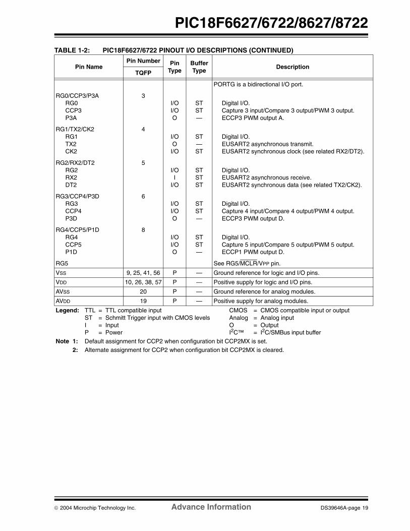
RG0/CCP3/P3ARG0CCP3P3A
3I/OI/OO
STST—
Digital I/O.Capture 3 input/Compare 3 output/PWM 3 output.ECCP3 PWM output A.
RG1/TX2/CK2RG1TX2CK2
4I/OOI/O
ST—ST
Digital I/O.EUSART2 asynchronous transmit. EUSART2 synchronous clock (see related RX2/DT2).
RG2/RX2/DT2RG2RX2DT2
5I/OI
I/O
STSTST
Digital I/O.EUSART2 asynchronous receive.EUSART2 synchronous data (see related TX2/CK2).
RG3/CCP4/P3DRG3CCP4P3D
6I/OI/OO
STST—
Digital I/O.Capture 4 input/Compare 4 output/PWM 4 output.ECCP3 PWM output D.
RG4/CCP5/P1DRG4CCP5P1D
8I/OI/OO
STST—
Digital I/O.Capture 5 input/Compare 5 output/PWM 5 output.ECCP1 PWM output D.
RG5 See RG5/MCLR/VPP pin.
VSS 9, 25, 41, 56 P — Ground reference for logic and I/O pins.
VDD 10, 26, 38, 57 P — Positive supply for logic and I/O pins.
AVSS 20 P — Ground reference for analog modules.
AVDD 19 P — Positive supply for analog modules.
TABLE 1-2: PIC18F6627/6722 PINOUT I/O DESCRIPTIONS (CONTINUED)
Pin NamePin Number Pin
TypeBufferType
DescriptionTQFP
Legend: TTL = TTL compatible input CMOS = CMOS compatible input or output ST = Schmitt Trigger input with CMOS levels Analog = Analog input I = Input O = Output P = Power I2C™ = I2C/SMBus input buffer
Note 1: Default assignment for CCP2 when configuration bit CCP2MX is set.2: Alternate assignment for CCP2 when configuration bit CCP2MX is cleared.

PIC18F6627/6722/8627/8722
DS39646A-page 20 Advance Information 2004 Microchip Technology Inc.
TABLE 1-3: PIC18F8627/8722 PINOUT I/O DESCRIPTIONS
Pin NamePin Number Pin
TypeBufferType
DescriptionTQFP
RG5/MCLR/VPP
RG5MCLR
VPP
9II
P
STST
Master Clear (input) or programming voltage (input).Digital input.Master Clear (Reset) input. This pin is an active-low Reset to the device.Programming voltage input.
OSC1/CLKI/RA7OSC1
CLKI
RA7
49I
I
I/O
ST
CMOS
TTL
Oscillator crystal or external clock input.Oscillator crystal input or external clock source input. ST buffer when configured in RC mode, CMOS otherwise.External clock source input. Always associated with pin function OSC1. (See related OSC1/CLKI, OSC2/CLKO pins.)General purpose I/O pin.
OSC2/CLKO/RA6OSC2
CLKO
RA6
50O
O
I/O
—
—
TTL
Oscillator crystal or clock output.Oscillator crystal output. Connects to crystal or resonator in Crystal Oscillator mode.In RC mode, OSC2 pin outputs CLKO, which has 1/4 the frequency of OSC1 and denotes theinstruction cycle rate. General purpose I/O pin.
Legend: TTL = TTL compatible input CMOS = CMOS compatible input or output ST = Schmitt Trigger input with CMOS levels Analog = Analog input I = Input O = Output P = Power I2C™/SMB = I2C/SMBus input buffer
Note 1: Alternate assignment for CCP2 when configuration bit CCP2MX is cleared (all operating modes except Microcontroller mode).
2: Default assignment for CCP2 in all operating modes (CCP2MX is set). 3: Alternate assignment for CCP2 when CCP2MX is cleared (Microcontroller mode only).4: Default assignment for P1B/P1C/P3B/P3C (ECCPMX is set).5: Alternate assignment for P1B/P1C/P3B/P3C (ECCPMX is clear).

2004 Microchip Technology Inc. Advance Information DS39646A-page 21
PIC18F6627/6722/8627/8722
PORTA is a bidirectional I/O port.
RA0/AN0RA0AN0
30I/OI
TTLAnalog
Digital I/O.Analog input 0.
RA1/AN1RA1AN1
29I/OI
TTLAnalog
Digital I/O.Analog input 1.
RA2/AN2/VREF-RA2AN2VREF-
28I/OII
TTLAnalogAnalog
Digital I/O.Analog input 2.A/D reference voltage (low) input.
RA3/AN3/VREF+RA3AN3VREF+
27I/OII
TTLAnalogAnalog
Digital I/O.Analog input 3.A/D reference voltage (high) input.
RA4/T0CKIRA4T0CKI
34I/OI
ST/ODST
Digital I/O. Open-drain when configured as output.Timer0 external clock input.
RA5/AN4/HLVDINRA5AN4HLVDIN
33I/OII
TTLAnalogAnalog
Digital I/O.Analog input 4. High/Low-Voltage Detect input.
RA6 See the OSC2/CLKO/RA6 pin.
RA7 See the OSC1/CLKI/RA7 pin.
TABLE 1-3: PIC18F8627/8722 PINOUT I/O DESCRIPTIONS (CONTINUED)
Pin NamePin Number Pin
TypeBufferType
DescriptionTQFP
Legend: TTL = TTL compatible input CMOS = CMOS compatible input or output ST = Schmitt Trigger input with CMOS levels Analog = Analog input I = Input O = Output P = Power I2C™/SMB = I2C/SMBus input buffer
Note 1: Alternate assignment for CCP2 when configuration bit CCP2MX is cleared (all operating modes except Microcontroller mode).
2: Default assignment for CCP2 in all operating modes (CCP2MX is set). 3: Alternate assignment for CCP2 when CCP2MX is cleared (Microcontroller mode only).4: Default assignment for P1B/P1C/P3B/P3C (ECCPMX is set).5: Alternate assignment for P1B/P1C/P3B/P3C (ECCPMX is clear).

PIC18F6627/6722/8627/8722
DS39646A-page 22 Advance Information 2004 Microchip Technology Inc.
PORTB is a bidirectional I/O port. PORTB can be software programmed for internal weak pull-ups on all inputs.
RB0/INT0/FLT0RB0INT0FLT0
58I/OII
TTLSTST
Digital I/O.External interrupt 0.PWM fault input for ECCPx.
RB1/INT1RB1INT1
57I/OI
TTLST
Digital I/O.External interrupt 1.
RB2/INT2RB2INT2
56I/OI
TTLST
Digital I/O.External interrupt 2.
RB3/INT3/CCP2/P2ARB3INT3CCP2(1)
P2A(1)
55I/OIOO
TTLST——
Digital I/O.External interrupt 3.Capture 2 input/Compare 2 output/PWM 2 output.ECCP2 PWM output A.
RB4/KBI0RB4KBI0
54I/OI
TTLTTL
Digital I/O.Interrupt-on-change pin.
RB5/KBI1/PGMRB5KBI1PGM
53I/OI
I/O
TTLTTLST
Digital I/O.Interrupt-on-change pin.Low-Voltage ICSP programming enable pin.
RB6/KBI2/PGCRB6KBI2PGC
52I/OI
I/O
TTLTTLST
Digital I/O.Interrupt-on-change pin. In-Circuit Debugger and ICSP™ programming clock pin.
RB7/KBI3/PGDRB7KBI3PGD
47I/OI
I/O
TTLTTLST
Digital I/O.Interrupt-on-change pin. In-Circuit Debugger and ICSP programming data pin.
TABLE 1-3: PIC18F8627/8722 PINOUT I/O DESCRIPTIONS (CONTINUED)
Pin NamePin Number Pin
TypeBufferType
DescriptionTQFP
Legend: TTL = TTL compatible input CMOS = CMOS compatible input or output ST = Schmitt Trigger input with CMOS levels Analog = Analog input I = Input O = Output P = Power I2C™/SMB = I2C/SMBus input buffer
Note 1: Alternate assignment for CCP2 when configuration bit CCP2MX is cleared (all operating modes except Microcontroller mode).
2: Default assignment for CCP2 in all operating modes (CCP2MX is set). 3: Alternate assignment for CCP2 when CCP2MX is cleared (Microcontroller mode only).4: Default assignment for P1B/P1C/P3B/P3C (ECCPMX is set).5: Alternate assignment for P1B/P1C/P3B/P3C (ECCPMX is clear).
2004 Microchip Technology Inc. Advance Information DS39646A-page 23
PIC18F6627/6722/8627/8722
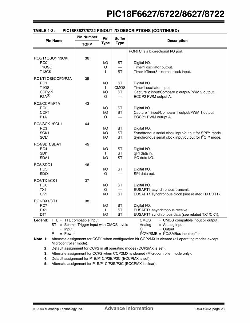
PORTC is a bidirectional I/O port.
RC0/T1OSO/T13CKIRC0T1OSOT13CKI
36I/OOI
ST—ST
Digital I/O.Timer1 oscillator output. Timer1/Timer3 external clock input.
RC1/T1OSI/CCP2/P2ARC1T1OSICCP2(2)
P2A(2)
35I/OI
I/OO
STCMOS
ST—
Digital I/O.Timer1 oscillator input.Capture 2 input/Compare 2 output/PWM 2 output.ECCP2 PWM output A.
RC2/CCP1/P1ARC2CCP1P1A
43I/OI/OO
STST—
Digital I/O.Capture 1 input/Compare 1 output/PWM 1 output.ECCP1 PWM outupt A.
RC3/SCK1/SCL1RC3SCK1SCL1
44I/OI/OI/O
STSTST
Digital I/O.Synchronous serial clock input/output for SPI™ mode.Synchronous serial clock input/output for I2C™ mode.
RC4/SDI1/SDA1RC4SDI1SDA1
45I/OI
I/O
STSTST
Digital I/O.SPI data in.I2C data I/O.
RC5/SDO1RC5SDO1
46I/OO
ST—
Digital I/O.SPI data out.
RC6/TX1/CK1RC6TX1CK1
37I/OO
I/O
ST—ST
Digital I/O.EUSART1 asynchronous transmit. EUSART1 synchronous clock (see related RX1/DT1).
RC7/RX1/DT1RC7RX1DT1
38I/OI
I/O
STSTST
Digital I/O.EUSART1 asynchronous receive.EUSART1 synchronous data (see related TX1/CK1).
TABLE 1-3: PIC18F8627/8722 PINOUT I/O DESCRIPTIONS (CONTINUED)
Pin NamePin Number Pin
TypeBufferType
DescriptionTQFP
Legend: TTL = TTL compatible input CMOS = CMOS compatible input or output ST = Schmitt Trigger input with CMOS levels Analog = Analog input I = Input O = Output P = Power I2C™/SMB = I2C/SMBus input buffer
Note 1: Alternate assignment for CCP2 when configuration bit CCP2MX is cleared (all operating modes except Microcontroller mode).
2: Default assignment for CCP2 in all operating modes (CCP2MX is set). 3: Alternate assignment for CCP2 when CCP2MX is cleared (Microcontroller mode only).4: Default assignment for P1B/P1C/P3B/P3C (ECCPMX is set).5: Alternate assignment for P1B/P1C/P3B/P3C (ECCPMX is clear).

PIC18F6627/6722/8627/8722
DS39646A-page 24 Advance Information 2004 Microchip Technology Inc.
PORTD is a bidirectional I/O port.
RD0/AD0/PSP0RD0AD0PSP0
72I/OI/OI/O
STTTLTTL
Digital I/O.External memory address/data 0.Parallel Slave Port data.
RD1/AD1/PSP1RD1AD1PSP1
69I/OI/OI/O
STTTLTTL
Digital I/O.External memory address/data 1.Parallel Slave Port data.
RD2/AD2/PSP2RD2AD2PSP2
68I/OI/OI/O
STTTLTTL
Digital I/O.External memory address/data 2.Parallel Slave Port data.
RD3/AD3/PSP3RD3AD3PSP3
67I/OI/OI/O
STTTLTTL
Digital I/O.External memory address/data 3.Parallel Slave Port data.
RD4/AD4/PSP4/SDO2RD4AD4PSP4SDO2
66I/OI/OI/OO
STTTLTTL—
Digital I/O.External memory address/data 4.Parallel Slave Port data.SPI data out.
RD5/AD5/PSP5/SDI2/SDA2
RD5AD5PSP5SDI2SDA2
65
I/OI/OI/OI
I/O
STTTLTTLST
I2C/SMB
Digital I/O.External memory address/data 5.Parallel Slave Port data.SPI data in.I2C data I/O.
RD6/AD6/PSP6/SCK2/SCL2
RD6AD6PSP6SCK2SCL2
64
I/OI/OI/OI/OI/O
STTTLTTLST
I2C/SMB
Digital I/O.External memory address/data 6.Parallel Slave Port data.Synchronous serial clock input/output for SPI mode.Synchronous serial clock input/output for I2C mode.
RD7/AD7/PSP7/SS2RD7AD7PSP7SS2
63I/OI/OI/OI
STTTLTTLTTL
Digital I/O.External memory address/data 7.Parallel Slave Port data.SPI Slave Select input.
TABLE 1-3: PIC18F8627/8722 PINOUT I/O DESCRIPTIONS (CONTINUED)
Pin NamePin Number Pin
TypeBufferType
DescriptionTQFP
Legend: TTL = TTL compatible input CMOS = CMOS compatible input or output ST = Schmitt Trigger input with CMOS levels Analog = Analog input I = Input O = Output P = Power I2C™/SMB = I2C/SMBus input buffer
Note 1: Alternate assignment for CCP2 when configuration bit CCP2MX is cleared (all operating modes except Microcontroller mode).
2: Default assignment for CCP2 in all operating modes (CCP2MX is set). 3: Alternate assignment for CCP2 when CCP2MX is cleared (Microcontroller mode only).4: Default assignment for P1B/P1C/P3B/P3C (ECCPMX is set).5: Alternate assignment for P1B/P1C/P3B/P3C (ECCPMX is clear).

2004 Microchip Technology Inc. Advance Information DS39646A-page 25
PIC18F6627/6722/8627/8722
PORTE is a bidirectional I/O port.
RE0/AD8/RD/P2DRE0AD8RDP2D
4I/OI/OIO
STTTLTTL—
Digital I/O.External memory address/data 8.Read control for Parallel Slave Port.ECCP2 PWM output D.
RE1/AD9/WR/P2CRE1AD9WRP2C
3I/OI/OIO
STTTLTTL—
Digital I/O.External memory address/data 9.Write control for Parallel Slave Port.ECCP2 PWM output C.
RE2/AD10/CS/P2BRE2AD10CSP2B
78I/OI/OIO
STTTLTTL—
Digital I/O.External memory address/data 10.Chip Select control for Parallel Slave Port.ECCP2 PWM output B.
RE3/AD11/P3CRE3AD11P3C(4)
77I/OI/OO
STTTL—
Digital I/O.External memory address/data 11.ECCP3 PWM output C.
RE4/AD12/P3BRE4AD12P3B(4)
76I/OI/OO
STTTL—
Digital I/O.External memory address/data 12.ECCP3 PWM output B.
RE5/AD13/P1CRE5AD13P1C(4)
75I/OI/OO
STTTL—
Digital I/O.External memory address/data 13.ECCP1 PWM output C.
RE6/AD14/P1BRE6AD14P1B(4)
74I/OI/OO
STTTL—
Digital I/O.External memory address/data 14.ECCP1 PWM output B.
RE7/AD15/CCP2/P2ARE7AD15CCP2(3)
P2A(3)
73I/OI/OI/OO
STTTLST—
Digital I/O.External memory address/data 15.Capture 2 input/Compare 2 output/PWM 2 output.ECCP2 PWM output A.
TABLE 1-3: PIC18F8627/8722 PINOUT I/O DESCRIPTIONS (CONTINUED)
Pin NamePin Number Pin
TypeBufferType
DescriptionTQFP
Legend: TTL = TTL compatible input CMOS = CMOS compatible input or output ST = Schmitt Trigger input with CMOS levels Analog = Analog input I = Input O = Output P = Power I2C™/SMB = I2C/SMBus input buffer
Note 1: Alternate assignment for CCP2 when configuration bit CCP2MX is cleared (all operating modes except Microcontroller mode).
2: Default assignment for CCP2 in all operating modes (CCP2MX is set). 3: Alternate assignment for CCP2 when CCP2MX is cleared (Microcontroller mode only).4: Default assignment for P1B/P1C/P3B/P3C (ECCPMX is set).5: Alternate assignment for P1B/P1C/P3B/P3C (ECCPMX is clear).

PIC18F6627/6722/8627/8722
DS39646A-page 26 Advance Information 2004 Microchip Technology Inc.
PORTF is a bidirectional I/O port.
RF0/AN5RF0AN5
24I/OI
STAnalog
Digital I/O.Analog input 5.
RF1/AN6/C2OUTRF1AN6C2OUT
23I/OIO
STAnalog
—
Digital I/O.Analog input 6.Comparator 2 output.
RF2/AN7/C1OUTRF2AN7C1OUT
18I/OIO
STAnalog
—
Digital I/O.Analog input 7.Comparator 1 output.
RF3/AN8RF3AN8
17I/OI
STAnalog
Digital I/O.Analog input 8.
RF4/AN9RF4AN9
16I/OI
STAnalog
Digital I/O.Analog input 9.
RF5/AN10/CVREF
RF5AN10CVREF
15I/OIO
STAnalogAnalog
Digital I/O.Analog input 10. Comparator reference voltage output.
RF6/AN11RF6AN11
14I/OI
STAnalog
Digital I/O.Analog input 11.
RF7/SS1RF7SS1
13I/OI
STTTL
Digital I/O.SPI slave select input.
TABLE 1-3: PIC18F8627/8722 PINOUT I/O DESCRIPTIONS (CONTINUED)
Pin NamePin Number Pin
TypeBufferType
DescriptionTQFP
Legend: TTL = TTL compatible input CMOS = CMOS compatible input or output ST = Schmitt Trigger input with CMOS levels Analog = Analog input I = Input O = Output P = Power I2C™/SMB = I2C/SMBus input buffer
Note 1: Alternate assignment for CCP2 when configuration bit CCP2MX is cleared (all operating modes except Microcontroller mode).
2: Default assignment for CCP2 in all operating modes (CCP2MX is set). 3: Alternate assignment for CCP2 when CCP2MX is cleared (Microcontroller mode only).4: Default assignment for P1B/P1C/P3B/P3C (ECCPMX is set).5: Alternate assignment for P1B/P1C/P3B/P3C (ECCPMX is clear).

2004 Microchip Technology Inc. Advance Information DS39646A-page 27
PIC18F6627/6722/8627/8722
PORTG is a bidirectional I/O port.
RG0/CCP3/P3ARG0CCP3P3A
5I/OI/OO
STST—
Digital I/O.Capture 3 input/Compare 3 output/PWM 3 output.ECCP3 PWM output A.
RG1/TX2/CK2RG1TX2CK2
6I/OO
I/O
ST—ST
Digital I/O.EUSART2 asynchronous transmit. EUSART2 synchronous clock (see related RX2/DT2).
RG2/RX2/DT2RG2RX2DT2
7I/OI
I/O
STSTST
Digital I/O.EUSART2 asynchronous receive.EUSART2 synchronous data (see related TX2/CK2).
RG3/CCP4/P3DRG3CCP4P3D
8I/OI/OO
STST—
Digital I/O.Capture 4 input/Compare 4 output/PWM 4 output.ECCP3 PWM output D.
RG4/CCP5/P1DRG4CCP5P1D
10I/OI/OO
STST—
Digital I/O.Capture 5 input/Compare 5 output/PWM 5 output.ECCP1 PWM output D.
RG5 See RG5/MCLR/VPP pin.
TABLE 1-3: PIC18F8627/8722 PINOUT I/O DESCRIPTIONS (CONTINUED)
Pin NamePin Number Pin
TypeBufferType
DescriptionTQFP
Legend: TTL = TTL compatible input CMOS = CMOS compatible input or output ST = Schmitt Trigger input with CMOS levels Analog = Analog input I = Input O = Output P = Power I2C™/SMB = I2C/SMBus input buffer
Note 1: Alternate assignment for CCP2 when configuration bit CCP2MX is cleared (all operating modes except Microcontroller mode).
2: Default assignment for CCP2 in all operating modes (CCP2MX is set). 3: Alternate assignment for CCP2 when CCP2MX is cleared (Microcontroller mode only).4: Default assignment for P1B/P1C/P3B/P3C (ECCPMX is set).5: Alternate assignment for P1B/P1C/P3B/P3C (ECCPMX is clear).
PIC18F6627/6722/8627/8722
DS39646A-page 28 Advance Information 2004 Microchip Technology Inc.
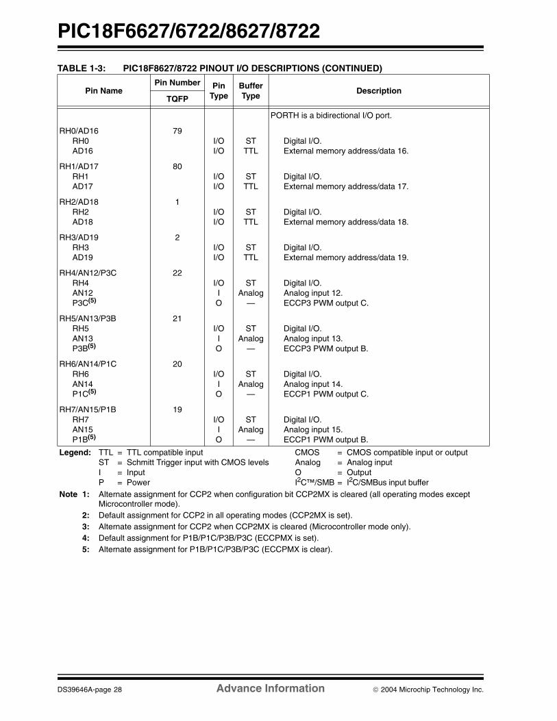
PORTH is a bidirectional I/O port.
RH0/AD16RH0AD16
79I/OI/O
STTTL
Digital I/O.External memory address/data 16.
RH1/AD17RH1AD17
80I/OI/O
STTTL
Digital I/O.External memory address/data 17.
RH2/AD18RH2AD18
1I/OI/O
STTTL
Digital I/O.External memory address/data 18.
RH3/AD19RH3AD19
2I/OI/O
STTTL
Digital I/O.External memory address/data 19.
RH4/AN12/P3CRH4AN12P3C(5)
22I/OIO
STAnalog
—
Digital I/O.Analog input 12.ECCP3 PWM output C.
RH5/AN13/P3BRH5AN13P3B(5)
21I/OIO
STAnalog
—
Digital I/O.Analog input 13.ECCP3 PWM output B.
RH6/AN14/P1CRH6AN14P1C(5)
20I/OIO
STAnalog
—
Digital I/O.Analog input 14.ECCP1 PWM output C.
RH7/AN15/P1BRH7AN15P1B(5)
19I/OIO
STAnalog
—
Digital I/O.Analog input 15.ECCP1 PWM output B.
TABLE 1-3: PIC18F8627/8722 PINOUT I/O DESCRIPTIONS (CONTINUED)
Pin NamePin Number Pin
TypeBufferType
DescriptionTQFP
Legend: TTL = TTL compatible input CMOS = CMOS compatible input or output ST = Schmitt Trigger input with CMOS levels Analog = Analog input I = Input O = Output P = Power I2C™/SMB = I2C/SMBus input buffer
Note 1: Alternate assignment for CCP2 when configuration bit CCP2MX is cleared (all operating modes except Microcontroller mode).
2: Default assignment for CCP2 in all operating modes (CCP2MX is set). 3: Alternate assignment for CCP2 when CCP2MX is cleared (Microcontroller mode only).4: Default assignment for P1B/P1C/P3B/P3C (ECCPMX is set).5: Alternate assignment for P1B/P1C/P3B/P3C (ECCPMX is clear).

2004 Microchip Technology Inc. Advance Information DS39646A-page 29
PIC18F6627/6722/8627/8722
PORTJ is a bidirectional I/O port.
RJ0/ALERJ0ALE
62I/OO
ST—
Digital I/O.External memory address latch enable.
RJ1/OERJ1OE
61I/OO
ST—
Digital I/O.External memory output enable.
RJ2/WRLRJ2WRL
60I/OO
ST—
Digital I/O.External memory write low control.
RJ3/WRHRJ3WRH
59I/OO
ST—
Digital I/O.External memory write high control.
RJ4/BA0RJ4BA0
39I/OO
ST—
Digital I/O.External memory Byte Address 0 control.
RJ5/CERJ4CE
40I/OO
ST—
Digital I/OExternal memory chip enable control.
RJ6/LBRJ6LB
41I/OO
ST—
Digital I/O.External memory low byte control.
RJ7/UBRJ7UB
42I/OO
ST—
Digital I/O.External memory high byte control.
VSS 11, 31, 51, 70 P — Ground reference for logic and I/O pins.
VDD 12, 32, 48, 71 P — Positive supply for logic and I/O pins.
AVSS 26 P — Ground reference for analog modules.
AVDD 25 P — Positive supply for analog modules.
TABLE 1-3: PIC18F8627/8722 PINOUT I/O DESCRIPTIONS (CONTINUED)
Pin NamePin Number Pin
TypeBufferType
DescriptionTQFP
Legend: TTL = TTL compatible input CMOS = CMOS compatible input or output ST = Schmitt Trigger input with CMOS levels Analog = Analog input I = Input O = Output P = Power I2C™/SMB = I2C/SMBus input buffer
Note 1: Alternate assignment for CCP2 when configuration bit CCP2MX is cleared (all operating modes except Microcontroller mode).
2: Default assignment for CCP2 in all operating modes (CCP2MX is set). 3: Alternate assignment for CCP2 when CCP2MX is cleared (Microcontroller mode only).4: Default assignment for P1B/P1C/P3B/P3C (ECCPMX is set).5: Alternate assignment for P1B/P1C/P3B/P3C (ECCPMX is clear).

PIC18F6627/6722/8627/8722
DS39646A-page 30 Advance Information 2004 Microchip Technology Inc.
NOTES:

2004 Microchip Technology Inc. Advance Information DS39646A-page 31
PIC18F6627/6722/8627/8722
2.0 OSCILLATOR CONFIGURATIONS
2.1 Oscillator Types
PIC18F6627/6722/8627/8722 devices can be operatedin ten different oscillator modes. The user can programthe configuration bits, FOSC3:FOSC0, in ConfigurationRegister 1H to select one of these ten modes:
1. LP Low-Power Crystal2. XT Crystal/Resonator3. HS High-Speed Crystal/Resonator
4. HSPLL High-Speed Crystal/Resonator with PLL enabled
5. RC External Resistor/Capacitor with FOSC/4 output on RA6
6. RCIO External Resistor/Capacitor with I/O on RA6
7. INTIO1 Internal Oscillator with FOSC/4 outputon RA6 and I/O on RA7
8. INTIO2 Internal Oscillator with I/O on RA6 and RA7
9. EC External Clock with FOSC/4 output10. ECIO External Clock with I/O on RA6
2.2 Crystal Oscillator/Ceramic Resonators
In XT, LP, HS or HSPLL Oscillator modes, a crystal orceramic resonator is connected to the OSC1 andOSC2 pins to establish oscillation. Figure 2-1 showsthe pin connections.
The oscillator design requires the use of a parallel cutcrystal.
FIGURE 2-1: CRYSTAL/CERAMIC RESONATOR OPERATION (XT, LP, HS OR HSPLL CONFIGURATION)
TABLE 2-1: CAPACITOR SELECTION FOR CERAMIC RESONATORS
Note: Use of a series cut crystal may give afrequency out of the crystal manufacturer’sspecifications.
Typical Capacitor Values Used:
Mode Freq OSC1 OSC2
XT 3.58 MHz 22 pF 22 pF
Capacitor values are for design guidance only.
Different capacitor values may be required to produceacceptable oscillator operation. The user should testthe performance of the oscillator over the expectedVDD and temperature range for the application. Referto the following application notes for oscillator specificinformation:
• AN588 – PIC16/17 Oscillator Design Guide• AN826 – Crystal Oscillator Basics and Crystal
Selection for rfPIC™ and PICmicro® Devices• AN843 – Speed Control of 3-Phase Induction
Motor Using PIC18 Microcontrollers• AN849 – Basic PICmicro® Oscillator Design
See the notes following Table 2-2 for additionalinformation.
Note: When using resonators with frequenciesabove 3.5 MHz, the use of HS mode,rather than XT mode, is recommended.HS mode may be used at any VDD forwhich the controller is rated. If HS isselected, it is possible that the gain of theoscillator will overdrive the resonator.Therefore, a series resistor may be placedbetween the OSC2 pin and the resonator.As a good starting point, therecommended value of RS is 330Ω.
Note 1: See Table 2-1 and Table 2-2 for initial values ofC1 and C2.
2: A series resistor (RS) may be required for ATstrip cut crystals.
3: RF varies with the oscillator mode chosen.
C1(1)
C2(1)
XTAL
OSC2
OSC1
RF(3)
Sleep
To
Logic
PIC18FXXXXRS(2)
Internal

PIC18F6627/6722/8627/8722
DS39646A-page 32 Advance Information 2004 Microchip Technology Inc.
TABLE 2-2: CAPACITOR SELECTION FOR QUARTZ CRYSTALS
An external clock source may also be connected to theOSC1 pin in the HS mode, as shown in Figure 2-2.When operated in this mode, parameters D033 andD043 apply.
FIGURE 2-2: EXTERNAL CLOCK INPUT OPERATION (HS OSC CONFIGURATION)
2.3 External Clock Input
The EC and ECIO Oscillator modes require an externalclock source to be connected to the OSC1 pin. There isno oscillator start-up time required after a Power-onReset or after an exit from Sleep mode.
In the EC Oscillator mode, the oscillator frequencydivided by 4 is available on the OSC2 pin. This signalmay be used for test purposes or to synchronize otherlogic. Figure 2-3 shows the pin connections for the ECOscillator mode.
FIGURE 2-3: EXTERNAL CLOCK INPUT OPERATION (EC CONFIGURATION)
The ECIO Oscillator mode functions like the EC mode,except that the OSC2 pin becomes an additional gen-eral purpose I/O pin. The I/O pin becomes bit 6 ofPORTA (RA6). Figure 2-4 shows the pin connectionsfor the ECIO Oscillator mode. When operated in thismode, parameters D033A and D043A apply.
FIGURE 2-4: EXTERNAL CLOCK INPUT OPERATION (ECIO CONFIGURATION)
Osc TypeCrystal
Freq
Typical Capacitor Values Tested:
C1 C2
LP 32 kHz 22 pF 22 pF
XT 1 MHz4 MHz
22 pF22 pF
22 pF22 pF
HS 4 MHz10 MHz20 MHz25 MHz
22 pF22 pF22 pF22 pF
22 pF22 pF22 pF22 pF
Capacitor values are for design guidance only.
Different capacitor values may be required to produceacceptable oscillator operation. The user should testthe performance of the oscillator over the expectedVDD and temperature range for the application. Referto the following application notes for oscillator specificinformation:
• AN588 – PIC16/17 Oscillator Design Guide• AN826 – Crystal Oscillator Basics and Crystal
Selection for rfPIC™ and PICmicro® Devices• AN843 – Speed Control of 3-Phase Induction
Motor Using PIC18 Microcontrollers• AN849 – Basic PICmicro® Oscillator Design
See the notes following this table for additionalinformation.
Note 1: Higher capacitance increases the stabilityof the oscillator but also increases thestart-up time.
2: When operating below 3V VDD, or whenusing certain ceramic resonators at anyvoltage, it may be necessary to use theHS mode or switch to a crystal oscillator.
3: Since each resonator/crystal has its owncharacteristics, the user should consultthe resonator/crystal manufacturer forappropriate values of externalcomponents.
4: Rs may be required to avoid overdrivingcrystals with low drive level specification.
5: Always verify oscillator performance overthe VDD and temperature range that isexpected for the application.
OSC1
OSC2Open
Clock fromExt. System PIC18FXXXX
(HS Mode)
OSC1/CLKI
OSC2/CLKOFOSC/4
Clock fromExt. System PIC18FXXXX
OSC1/CLKI
I/O (OSC2)RA6
Clock fromExt. System PIC18FXXXX

2004 Microchip Technology Inc. Advance Information DS39646A-page 33
PIC18F6627/6722/8627/8722
2.4 RC Oscillator
For timing insensitive applications, the RC and RCIOOscillator modes offer additional cost savings. Theactual oscillator frequency is a function of severalfactors:
• supply voltage
• values of the external resistor (REXT) and capacitor (CEXT)
• operating temperature
Given the same device, operating voltage and tempera-ture and component values, there will also be unit-to-unitfrequency variations. These are due to factors such as:
• normal manufacturing variation• difference in lead frame capacitance between
package types (especially for low CEXT values) • variations within the tolerance of limits of REXT
and CEXT
In the RC Oscillator mode, the oscillator frequencydivided by 4 is available on the OSC2 pin. This signalmay be used for test purposes or to synchronize otherlogic. Figure 2-5 shows how the R/C combination isconnected.
FIGURE 2-5: RC OSCILLATOR MODE
The RCIO Oscillator mode (Figure 2-6) functions likethe RC mode, except that the OSC2 pin becomes anadditional general purpose I/O pin. The I/O pinbecomes bit 6 of PORTA (RA6).
FIGURE 2-6: RCIO OSCILLATOR MODE
2.5 PLL Frequency Multiplier
A Phase Locked Loop (PLL) circuit is provided as anoption for users who wish to use a lower frequencyoscillator circuit or to clock the device up to its highestrated frequency from a crystal oscillator. This may beuseful for customers who are concerned with EMI dueto high-frequency crystals or users who require higherclock speeds from an internal oscillator.
2.5.1 HSPLL OSCILLATOR MODE
The HSPLL mode makes use of the HS mode oscillatorfor frequencies up to 10 MHz. A PLL then multiplies theoscillator output frequency by 4 to produce an internalclock frequency up to 40 MHz. The PLLEN bit is notavailable when this mode is configured as the primaryclock source.
The PLL is only available to the crystal oscillator whenthe FOSC3:FOSC0 configuration bits are programmedfor HSPLL mode (= 0110).
FIGURE 2-7: HSPLL BLOCK DIAGRAM
2.5.2 PLL AND INTOSC
The PLL is also available to the internal oscillator blockwhen the internal oscillator block is configured as theprimary clock source. In this configuration, the PLL isenabled in software and generates a clock output of upto 32 MHz. The operation of INTOSC with the PLL isdescribed in Section 2.6.4 “PLL in INTOSC Modes”.
OSC2/CLKO
CEXT
REXT
PIC18FXXXX
OSC1
FOSC/4
InternalClock
VDD
VSS
Recommended values: 3 kΩ ≤ REXT ≤ 100 kΩ20 pF ≤ CEXT ≤ 300 pF
CEXT
REXT
PIC18FXXXX
OSC1 InternalClock
VDD
VSS
Recommended values: 3 kΩ ≤ REXT ≤ 100 kΩ20 pF ≤ CEXT ≤ 300 pF
I/O (OSC2)RA6
MU
X
VCO
LoopFilter
Crystal
Osc
OSC2
OSC1
PLL Enable
FIN
FOUT
SYSCLK
PhaseComparator
HS Oscillator Enable
÷4
(from Configuration Register 1H)
HS Mode

PIC18F6627/6722/8627/8722
DS39646A-page 34 Advance Information 2004 Microchip Technology Inc.
2.6 Internal Oscillator Block
The PIC18F6627/6722/8627/8722 devices include aninternal oscillator block which generates two differentclock signals; either can be used as the micro-controller’s clock source. This may eliminate the needfor external oscillator circuits on the OSC1 and/orOSC2 pins.
The main output (INTOSC) is an 8 MHz clock source,which can be used to directly drive the device clock. Italso drives a postscaler, which can provide a range ofclock frequencies from 31 kHz to 4 MHz. The INTOSCoutput is enabled when a clock frequency from 125 kHzto 8 MHz is selected. The INTOSC output can also beenabled when 31 kHz is selected, depending on theINTSRC bit (OSCTUNE<7>).
The other clock source is the internal RC oscillator(INTRC), which provides a nominal 31 kHz output.INTRC is enabled if it is selected as the device clocksource; it is also enabled automatically when any of thefollowing are enabled:
• Power-up Timer• Fail-Safe Clock Monitor• Watchdog Timer
• Two-Speed Start-up
These features are discussed in greater detail inSection 25.0 “Special Features of the CPU”.
The clock source frequency (INTOSC direct, INTRCdirect or INTOSC postscaler) is selected by configuringthe IRCF bits of the OSCCON register (page 39).
2.6.1 INTIO MODES
Using the internal oscillator as the clock source elimi-nates the need for up to two external oscillator pins,which can then be used for digital I/O. Two distinctconfigurations are available:
• In INTIO1 mode, the OSC2 pin outputs FOSC/4, while OSC1 functions as RA7 (see Figure 2-8) for digital input and output.
• In INTIO2 mode, OSC1 functions as RA7 and OSC2 functions as RA6 (see Figure 2-9), both for digital input and output.
FIGURE 2-8: INTIO1 OSCILLATOR MODE
FIGURE 2-9: INTIO2 OSCILLATOR MODE
2.6.2 INTOSC OUTPUT FREQUENCY
The internal oscillator block is calibrated at the factoryto produce an INTOSC output frequency of 8 MHz.
The INTRC oscillator operates independently of theINTOSC source. Any changes in INTOSC acrossvoltage and temperature are not necessarily reflectedby changes in INTRC or vice versa.
2.6.3 OSCTUNE REGISTER
The INTOSC output has been calibrated at thefactory but can be adjusted in the user’s application.This is done by writing to TUN4:TUN0(OSCTUNE<4:0>) in the OSCTUNE register(Register 2-1).
When the OSCTUNE register is modified, the INTOSCfrequency will begin shifting to the new frequency. TheINTOSC clock will stabilize within 1 ms. Code execu-tion continues during this shift. There is no indicationthat the shift has occurred. The INTRC is not affectedby OSCTUNE.
The OSCTUNE register also implements the INTSRC(OSCTUNE<7>) and PLLEN (OSCTUNE<6>) bits,which control certain features of the internal oscillatorblock. The INTSRC bit allows users to select whichinternal oscillator provides the clock source when the31 kHz frequency option is selected. This is covered ingreater detail in Section 2.7.1 “Oscillator ControlRegister”.
The PLLEN bit controls the operation of the PhaseLocked Loop (PLL) in internal oscillator modes (seeFigure 2-10).
FIGURE 2-10: INTOSC AND PLL BLOCK DIAGRAM
PIC18FXXXXOSC2FOSC/4
I/O (OSC1)RA7
PIC18FXXXXI/O (OSC2)RA6
I/O (OSC1)RA7
MU
X
VCO
LoopFilter
OSC2
PLLEN
FIN
FOUT
SYSCLK
PhaseComparator
8 or 4 MHz
÷4
(OSCTUNE<6>)
MU
X
RA6
CLKOUT
INTOSC

2004 Microchip Technology Inc. Advance Information DS39646A-page 35
PIC18F6627/6722/8627/8722
2.6.4 PLL IN INTOSC MODES
The 4x Phase Locked Loop (PLL) can be used with theinternal oscillator block to produce faster device clockspeeds than are normally possible with the internaloscillator sources. When enabled, the PLL produces aclock speed of 16 MHz or 32 MHz.
Unlike HSPLL mode, the PLL is controlled throughsoftware. The control bit, PLLEN (OSCTUNE<6>), isused to enable or disable its operation.
The PLL is available when the device is configured touse the internal oscillator block as its primary clocksource (FOSC3:FOSC0 = 1001 or 1000). Additionally,the PLL will only function when the selected output fre-quency is either 4 MHz or 8 MHz (OSCCON<6:4> = 111or 110). If both of these conditions are not met, the PLLis disabled, and the PLLEN bit remains clear (writes areignored).
2.6.5 INTOSC FREQUENCY DRIFT
The factory calibrates the internal oscillator blockoutput (INTOSC) for 8 MHz. However, this frequencymay drift as VDD or temperature changes, and canaffect the controller operation in a variety of ways. It ispossible to adjust the INTOSC frequency by modifyingthe value in the OSCTUNE register. Depending on thedevice, this may have no effect on the INTRC clocksource frequency.
Tuning the INTOSC source requires knowing when tomake the adjustment, in which direction it should bemade and in some cases, how large a change isneeded. Three compensation techniques are discussedin Section 2.6.5.1 “Compensating with the USART”,Section 2.6.5.2 “Compensating with the Timers” andSection 2.6.5.3 “Compensating with the CCP Modulein Capture Mode”, but other techniques may be used.
REGISTER 2-1: OSCTUNE: OSCILLATOR TUNING REGISTER R/W-0 R/W-0 U-0 R/W-0 R/W-0 R/W-0 R/W-0 R/W-0
INTSRC PLLEN(1) — TUN4 TUN3 TUN2 TUN1 TUN0
bit 7 bit 0
bit 7 INTSRC: Internal Oscillator Low-Frequency Source Select bit
1 = 31.25 kHz device clock derived from 8 MHz INTOSC source (divide-by-256 enabled)0 = 31 kHz device clock derived directly from INTRC internal oscillator
bit 6 PLLEN: Frequency Multiplier PLL for INTOSC Enable bit(1)
1 = PLL enabled for INTOSC (4 MHz and 8 MHz only)0 = PLL disabled
Note 1: Available only in certain oscillator configurations; otherwise, this bit is unavailableand reads as ‘0’. See Section 2.6.4 “PLL in INTOSC Modes” for details.
bit 5 Unimplemented: Read as ‘0’
bit 4-0 TUN4:TUN0: Frequency Tuning bits01111 = Maximum frequency• •• •00001 00000 = Center frequency. Oscillator module is running at the calibrated frequency.11111 • •• •10000 = Minimum frequency
Legend:R = Readable bit W = Writable bit U = Unimplemented bit, read as ‘0’-n = Value at POR ‘1’ = Bit is set ‘0’ = Bit is cleared x = Bit is unknown
PIC18F6627/6722/8627/8722
DS39646A-page 36 Advance Information 2004 Microchip Technology Inc.
2.6.5.1 Compensating with the USART
An adjustment may be required when the USARTbegins to generate framing errors or receives data witherrors while in Asynchronous mode. Framing errorsindicate that the device clock frequency is too high. Toadjust for this, decrement the value in OSCTUNE toreduce the clock frequency. On the other hand, errorsin data may suggest that the clock speed is too low. Tocompensate, increment OSCTUNE to increase theclock frequency.
2.6.5.2 Compensating with the Timers
This technique compares device clock speed to somereference clock. Two timers may be used; one timer isclocked by the peripheral clock, while the other isclocked by a fixed reference source, such as theTimer1 oscillator.
Both timers are cleared, but the timer clocked by thereference generates interrupts. When an interruptoccurs, the internally clocked timer is read and bothtimers are cleared. If the internally clocked timer valueis much greater than expected, then the internal oscil-lator block is running too fast. To adjust for this, decre-ment the OSCTUNE register.
2.6.5.3 Compensating with the CCP Module in Capture Mode
A CCP module can use free running Timer1 (orTimer3), clocked by the internal oscillator block and anexternal event with a known period (i.e., AC powerfrequency). The time of the first event is captured in theCCPRxH:CCPRxL registers and is recorded for uselater. When the second event causes a capture, thetime of the first event is subtracted from the time of thesecond event. Since the period of the external event isknown, the time difference between events can becalculated.
If the measured time is much greater than thecalculated time, the internal oscillator block is runningtoo fast. To compensate, decrement the OSCTUNEregister. If the measured time is much less than thecalculated time, the internal oscillator block is runningtoo slow. To compensate, increment the OSCTUNEregister.

2004 Microchip Technology Inc. Advance Information DS39646A-page 37
PIC18F6627/6722/8627/8722
2.7 Clock Sources and Oscillator Switching
Like previous PIC18 devices, the PIC18F6627/6722/8627/8722 family includes a feature that allows thedevice clock source to be switched from the mainoscillator to an alternate clock source. PIC18F6627/6722/8627/8722 devices offer two alternate clock sources.When an alternate clock source is enabled, the variouspower-managed operating modes are available.
Essentially, there are three clock sources for thesedevices:
• Primary oscillators
• Secondary oscillators• Internal oscillator block
The primary oscillators include the External Crystaland Resonator modes, the External RC modes, theExternal Clock modes and the internal oscillator block.The particular mode is defined by the FOSC3:FOSC0configuration bits. The details of these modes arecovered earlier in this chapter.
The secondary oscillators are those external sourcesnot connected to the OSC1 or OSC2 pins. Thesesources may continue to operate even after thecontroller is placed in a power-managed mode.
PIC18F6627/6722/8627/8722 devices offer the Timer1oscillator as a secondary oscillator. This oscillator, in allpower-managed modes, is often the time base forfunctions such as a real-time clock.
Most often, a 32.768 kHz watch crystal is connectedbetween the RC0/T1OSO/T13CKI and RC1/T1OSIpins. Like the LP mode oscillator circuit, loadingcapacitors are also connected from each pin to ground.
The Timer1 oscillator is discussed in greater detail inSection 13.3 “Timer1 Oscillator”.
In addition to being a primary clock source, the internaloscillator block is available as a power-managedmode clock source. The INTRC source is also used asthe clock source for several special features, such asthe WDT and Fail-Safe Clock Monitor.
The clock sources for the PIC18F6627/6722/8627/8722devices are shown in Figure 2-11. See Section 25.0“Special Features of the CPU” for Configurationregister details.
FIGURE 2-11: PIC18F6627/6722/8627/8722 CLOCK DIAGRAM
PIC18F6627/6722/8675/8722
4 x PLL
FOSC3:FOSC0
Secondary Oscillator
T1OSCENEnableOscillator
T1OSO
T1OSI
Clock Source Option for other Modules
OSC1
OSC2
Sleep HSPLL, INTOSC/PLL
LP, XT, HS, RC, EC
T1OSC
CPU
Peripherals
IDLEN
Pos
tsca
ler
MU
X
MU
X
8 MHz
4 MHz
2 MHz
1 MHz
500 kHz
125 kHz
250 kHz
OSCCON<6:4>
111
110
101
100
011
010
001
00031 kHz
INTRCSource
InternalOscillator
Block
WDT, PWRT, FSCM
8 MHz
Internal Oscillator
(INTOSC)
OSCCON<6:4>
ClockControl
OSCCON<1:0>
Source8 MHz
31 kHz (INTRC)
OSCTUNE<6>
01
OSCTUNE<7>
and Two-Speed Start-up
Primary Oscillator

PIC18F6627/6722/8627/8722
DS39646A-page 38 Advance Information 2004 Microchip Technology Inc.
2.7.1 OSCILLATOR CONTROL REGISTER
The OSCCON register (Register 2-2) controls severalaspects of the device clock’s operation, both in fullpower operation and in power-managed modes.
The System Clock Select bits, SCS1:SCS0, select theclock source. The available clock sources are theprimary clock (defined by the FOSC3:FOSC0 configu-ration bits), the secondary clock (Timer1 oscillator) andthe internal oscillator block. The clock source changesimmediately after either of the SCSI:SCSO bits arechanged, following a brief clock transition interval. TheSCS bits are reset on all forms of Reset.
The Internal Oscillator Frequency Select bits(IRCF2:IRCF0) select the frequency output of theinternal oscillator block to drive the device clock. Thechoices are the INTRC source (31 kHz), the INTOSCsource (8 MHz) or one of the frequencies derived fromthe INTOSC postscaler (31.25 kHz to 4 MHz). If theinternal oscillator block is supplying the device clock,changing the states of these bits will have an immedi-ate change on the internal oscillator’s output. Ondevice Resets, the default output frequency of theinternal oscillator block is set at 1 MHz.
When a nominal output frequency of 31 kHz is selected(IRCF2:IRCF0 = 000), users may choose whichinternal oscillator acts as the source. This is done withthe INTSRC bit in the OSCTUNE register(OSCTUNE<7>). Setting this bit selects INTOSC as a31.25 kHz clock source derived from the INTOSCpostscaler. Clearing INTSRC selects INTRC (nominally31 kHz) as the clock source, and disables the INTOSCto reduce current consumption.
This option allows users to select the tunable and moreprecise INTOSC as a clock source, while maintainingpower savings with a very low clock speed. Addition-ally, the INTOSC source will already be stable should aswitch to a higher frequency be needed quickly.Regardless of the setting of INTSRC, INTRC alwaysremains the clock source for features such as theWatchdog Timer and the Fail-Safe Clock Monitor.
The OSTS, IOFS and T1RUN bits indicate which clocksource is currently providing the device clock. TheOSTS bit indicates that the Oscillator Start-up Timerand PLL Start-up Timer (if enabled) have timed out, andthe primary clock is providing the device clock inprimary clock modes. The IOFS bit indicates when theinternal oscillator block has stabilized and is providingthe device clock in RC Clock modes. The T1RUN bit(T1CON<6>) indicates when the Timer1 oscillator isproviding the device clock in secondary clock modes.In power-managed modes, only one of these three bitswill be set at any time. If none of these bits are set, theINTRC is providing the clock or the internal oscillatorblock has just started and is not yet stable.
The IDLEN bit controls whether the device goes intoSleep mode or one of the Idle modes when the SLEEPinstruction is executed.
The use of the flag and control bits in the OSCCONregister is discussed in more detail in Section 3.0“Power-Managed Modes”.
2.7.2 OSCILLATOR TRANSITIONS
PIC18F6627/6722/8627/8722 devices contain circuitryto prevent clock “glitches” when switching betweenclock sources. A short pause in the device clock occursduring the clock switch. The length of this pause is thesum of two cycles of the old clock source and three tofour cycles of the new clock source. This formulaassumes that the new clock source is stable.
Clock transitions are discussed in greater detail inSection 3.1.2 “Entering power-managed Modes”.
Note 1: The Timer1 oscillator must be enabled toselect the secondary clock source. TheTimer1 oscillator is enabled by setting theT1OSCEN bit in the Timer1 Control regis-ter (T1CON<3>). If the Timer1 oscillatoris not enabled, then any attempt to selecta secondary clock source will be ignored.
2: It is recommended that the Timer1oscillator be operating and stable beforeselecting the secondary clock source or avery long delay may occur while theTimer1 oscillator starts.

2004 Microchip Technology Inc. Advance Information DS39646A-page 39
PIC18F6627/6722/8627/8722
REGISTER 2-2: OSCCON: OSCILLATOR CONTROL REGISTER R/W-0 R/W-1 R/W-0 R/W-0 R(1) R-0 R/W-0 R/W-0
IDLEN IRCF2 IRCF1 IRCF0 OSTS IOFS SCS1 SCS0
bit 7 bit 0
bit 7 IDLEN: Idle Enable bit1 = Device enters an idle mode when a SLEEP instruction is executed0 = Device enters Sleep mode when a SLEEP instruction is executed
bit 6-4 IRCF2:IRCF0: Internal Oscillator Frequency Select bits(5)
111 = 8 MHz (INTOSC drives clock directly)110 = 4 MHz 101 = 2 MHz 100 = 1 MHz(3)
011 = 500 kHz 010 = 250 kHz001 = 125 kHz000 = 31 kHz (from either INTOSC/256 or INTRC directly)(2)
bit 3 OSTS: Oscillator Start-up Time-out Status bit(1)
1 = Oscillator start-up time-out timer (OST) has expired; primary oscillator is running0 = Oscillator start-up time-out timer (OST) is running; primary oscillator is not ready
bit 2 IOFS: INTOSC Frequency Stable bit 1 = INTOSC frequency is stable0 = INTOSC frequency is not stable
bit 1-0 SCS1:SCS0: System Clock Select bits(4)
1x = Internal oscillator block01 = Secondary (Timer1) oscillator00 = Primary oscillator
Note 1: Reset state depends on state of the IESO configuration bit.
2: Source selected by the INTSRC bit (OSCTUNE<7>), see text.
3: Default output frequency of INTOSC on Reset.
4: Modifying the SCSI:SCSO bits will cause an immediate clock source switch.
5: Modifying the IRCF3:IRCF0 bits will cause an immediate clock frequency switch ifthe internal oscillator is providing the device clocks.
Legend:R = Readable bit W = Writable bit U = Unimplemented bit, read as ‘0’-n = Value at POR ‘1’ = Bit is set ‘0’ = Bit is cleared x = Bit is unknown

PIC18F6627/6722/8627/8722
DS39646A-page 40 Advance Information 2004 Microchip Technology Inc.
2.8 Effects of Power-Managed Modes on the Various Clock Sources
When PRI_IDLE mode is selected, the configuredoscillator continues to run without interruption. For allother power-managed modes, the oscillator using theOSC1 pin is disabled. The OSC1 pin (and OSC2 pin incrystal oscillator modes) will stop oscillating.
In secondary clock modes (SEC_RUN andSEC_IDLE), the Timer1 oscillator is operating and pro-viding the device clock. The Timer1 oscillator may alsorun in all power-managed modes if required to clockTimer1 or Timer3.
In internal oscillator modes (RC_RUN and RC_IDLE),the internal oscillator block provides the device clocksource. The 31 kHz INTRC output can be used directlyto provide the clock and may be enabled to supportvarious special features, regardless of the power-managed mode (see Section 25.2 “Watchdog Timer(WDT)” and Section 25.4 “Fail-Safe Clock Monitor”for more information). The INTOSC output at 8 MHzmay be used directly to clock the device or may bedivided down by the postscaler. The INTOSC output isdisabled if the clock is provided directly from the INTRCoutput. The INTOSC output is also enabled for Two-Speed Start-up at 1 MHz after resets, and whenconfigured for wake from Sleep mode.
If the Sleep mode is selected, all clock sources arestopped. Since all the transistor switching currentshave been stopped, Sleep mode achieves the lowestcurrent consumption of the device (only leakagecurrents).
Enabling any on-chip feature that will operate duringSleep will increase the current consumed during Sleep.The INTRC is required to support WDT operation. TheTimer1 oscillator may be operating to support a real-time clock. Other features may be operating that do notrequire a device clock source (i.e., SSP slave, PSP,INTn pins and others). Peripherals that may addsignificant current consumption are listed inSection 28.2 “DC Characteristics”.
2.9 Power-up Delays
Power-up delays are controlled by two or three timers,so that no external Reset circuitry is required for mostapplications. The delays ensure that the device is keptin Reset until the device power supply is stable undernormal circumstances and the primary clock is operat-ing and stable. For additional information on power-updelays, see Section 4.5 “Device Reset Timers”.
The first timer is the Power-up Timer (PWRT), whichprovides a fixed delay on power-up (parameter 33,Table 28-12). It is enabled by clearing (= 0) thePWRTEN configuration bit (CONFIG2L<0>).
2.9.1 DELAYS FOR POWER-UP AND RETURN TO PRIMARY CLOCK
The second timer is the Oscillator Start-up Timer(OST), intended to delay execution until the crystaloscillator is stable (LP, XT and HS modes). The OSTdoes this by counting 1024 oscillator cycles beforeallowing the oscillator to clock the device.
When the HSPLL Oscillator mode is selected, a thirdtimer delays execution for an additional 2 ms, followingthe HS mode OST delay, so the PLL can lock to theincoming clock frequency. At the end of these delays,the OSTS bit (OSCCON<3>) is set.
There is a delay of interval TCSD (parameter 38,Table 28-12), once exeuction is alowed to start, whenthe controller becomes ready to execute instructions.This delay runs concurrently with any other delays.This may be the only delay that occurs when any of theEC, RC or INTIO modes are used as the primary clocksource.
TABLE 2-3: OSC1 AND OSC2 PIN STATES IN SLEEP MODE
OSC Mode OSC1 Pin OSC2 Pin
RC, INTIO1 Floating, external resistor pulls high At logic low (clock/4 output)
RCIO Floating, external resistor pulls high Configured as PORTA, bit 6
INTIO2 Configured as PORTA, bit 7 Configured as PORTA, bit 6
ECIO Floating, driven by external clock Configured as PORTA, bit 6
EC Floating, driven by external clock At logic low (clock/4 output)
LP, XT and HS Feedback inverter disabled at quiescent voltage level
Feedback inverter disabled at quiescent voltage level
Note: See Table 4-2 in Section 4.0 “Reset” for time-outs due to Sleep and MCLR Reset.

2004 Microchip Technology Inc. Advance Information DS39646A-page 41
PIC18F6627/6722/8627/8722
3.0 POWER-MANAGED MODES
PIC18F6627/6722/8627/8722 devices offer a total ofseven operating modes for more efficient power man-agement. These modes provide a variety of options forselective power conservation in applications whereresources may be limited (i.e., battery-powereddevices).
There are three categories of power-managed modes:
• Run modes• Idle modes
• Sleep mode
These categories define which portions of the deviceare clocked and sometimes, what speed. The Run andIdle modes may use any of the three available clocksources (primary, secondary or internal oscillatorblock); the Sleep mode does not use a clock source.
The power-managed modes include several power-saving features offered on previous PICmicro devices.One is the clock switching feature, offered in otherPIC18 devices, allowing the controller to use theTimer1 oscillator in place of the primary oscillator. Alsoincluded is the Sleep mode, offered by all PICmicrodevices, where all device clocks are stopped.
3.1 Selecting Power-Managed Modes
Selecting a power-managed mode requires twodecisions: if the CPU is to be clocked or not and theselection of a clock source. The IDLEN bit(OSCCON<7>) controls CPU clocking, while theSCS1:SCS0 bits (OSCCON<1:0>) select the clocksource. The individual modes, bit settings, clock sourcesand affected modules are summarized in Table 3-1.
3.1.1 CLOCK SOURCES
The SCS1:SCS0 bits allow the selection of one of threeclock sources for power-managed modes. They are:
• the primary clock, as defined by the FOSC3:FOSC0 configuration bits
• the secondary clock (the Timer1 oscillator)• the internal oscillator block (for INTOSC modes)
3.1.2 ENTERING POWER-MANAGED MODES
Switching from one power-managed mode to anotherbegins by loading the OSCCON register. TheSCS1:SCS0 bits select the clock source and determinewhich Run or Idle mode is to be used. Changing thesebits causes an immediate switch to the new clocksource, assuming that it is running. The switch mayalso be subject to clock transition delays. These arediscussed in Section 3.1.3 “Clock Transitions andStatus Indicators” and subsequent sections.
Entry to the power-managed Idle or Sleep modes istriggered by the execution of a SLEEP instruction. Theactual mode that results depends on the status of theIDLEN bit.
Depending on the current mode and the mode beingswitched to, a change to a power-managed mode doesnot always require setting all of these bits. Manytransitions may be done by changing the oscillator selectbits, or changing the IDLEN bit, prior to issuing a SLEEPinstruction. If the IDLEN bit is already configuredcorrectly, it may only be necessary to perform a SLEEPinstruction to switch to the desired mode.
TABLE 3-1: POWER-MANAGED MODES
Mode
OSCCON Bits Module Clocking
Available Clock and Oscillator SourceIDLEN(1)
<7>SCS1:SCS0
<1:0>CPU Peripherals
Sleep 0 N/A Off Off None – All clocks are disabled
PRI_RUN N/A 00 Clocked Clocked Primary – LP, XT, HS, HSPLL, RC, EC and Internal Oscillator Block(2).This is the normal full power execution mode.
SEC_RUN N/A 01 Clocked Clocked Secondary – Timer1 Oscillator
RC_RUN N/A 1x Clocked Clocked Internal Oscillator Block(2)
PRI_IDLE 1 00 Off Clocked Primary – LP, XT, HS, HSPLL, RC, EC
SEC_IDLE 1 01 Off Clocked Secondary – Timer1 Oscillator
RC_IDLE 1 1x Off Clocked Internal Oscillator Block(2)
Note 1: IDLEN reflects its value when the SLEEP instruction is executed.2: Includes INTOSC and INTOSC postscaler, as well as the INTRC source.

PIC18F6627/6722/8627/8722
DS39646A-page 42 Advance Information 2004 Microchip Technology Inc.
3.1.3 CLOCK TRANSITIONS AND STATUS INDICATORS
The length of the transition between clock sources isthe sum of two cycles of the old clock source and threeto four cycles of the new clock source. This formulaassumes that the new clock source is stable.
Three bits indicate the current clock source and itsstatus. They are:
• OSTS (OSCCON<3>) • IOFS (OSCCON<2>)
• T1RUN (T1CON<6>)
In general, only one of these bits will be set while in agiven power-managed mode. When the OSTS bit isset, the primary clock is providing the device clock.When the IOFS bit is set, the INTOSC output isproviding a stable 8 MHz clock source to a divider thatactually drives the device clock. When the T1RUN bit isset, the Timer1 oscillator is providing the clock. If noneof these bits are set, then either the INTRC clocksource is clocking the device, or the INTOSC source isnot yet stable.
If the internal oscillator block is configured as the pri-mary clock source by the FOSC3:FOSC0 configurationbits, then both the OSTS and IOFS bits may be setwhen in PRI_RUN or PRI_IDLE modes. This indicatesthat the primary clock (INTOSC output) is generating astable 8 MHz output. Entering another INTOSC power-managed mode at the same frequency would clear theOSTS bit.
3.1.4 MULTIPLE SLEEP COMMANDS
The power-managed mode that is invoked with theSLEEP instruction is determined by the setting of theIDLEN bit at the time the instruction is executed. Ifanother SLEEP instruction is executed, the device willenter the power-managed mode specified by IDLEN atthat time. If IDLEN has changed, the device will enterthe new power-managed mode specified by the newsetting.
3.2 Run Modes
In the Run modes, clocks to both the core andperipherals are active. The difference between thesemodes is the clock source.
3.2.1 PRI_RUN MODE
The PRI_RUN mode is the normal, full power executionmode of the microcontroller. This is also the defaultmode upon a device Reset, unless Two-Speed Start-upis enabled (see Section 25.3 “Two-Speed Start-up”for details). In this mode, the OSTS bit is set. The IOFSbit may be set if the internal oscillator block is the pri-mary clock source (see Section 2.7.1 “OscillatorControl Register”).
3.2.2 SEC_RUN MODE
The SEC_RUN mode is the compatible mode to the“clock switching” feature offered in other PIC18devices. In this mode, the CPU and peripherals areclocked from the Timer1 oscillator. This gives users theoption of lower power consumption while still using ahigh accuracy clock source.
SEC_RUN mode is entered by setting the SCS1:SCS0bits to ‘01’. The device clock source is switched to theTimer1 oscillator (see Figure 3-1), the primary oscilla-tor is shut down, the T1RUN bit (T1CON<6>) is set andthe OSTS bit is cleared.
On transitions from SEC_RUN mode to PRI_RUN, theperipherals and CPU continue to be clocked from theTimer1 oscillator while the primary clock is started.When the primary clock becomes ready, a clock switchback to the primary clock occurs (see Figure 3-2).When the clock switch is complete, the T1RUN bit iscleared, the OSTS bit is set and the primary clock isproviding the clock. The IDLEN and SCS bits are notaffected by the wake-up; the Timer1 oscillatorcontinues to run.
Note 1: Caution should be used when modifying asingle IRCF bit. If VDD is less than 3V, it ispossible to select a higher clock speedthan is supported by the low VDD.Improper device operation may result ifthe VDD/FOSC specifications are violated.
2: Executing a SLEEP instruction does notnecessarily place the device into Sleepmode. It acts as the trigger to place thecontroller into either the Sleep mode orone of the Idle modes, depending on thesetting of the IDLEN bit.
Note: The Timer1 oscillator should already berunning prior to entering SEC_RUN mode.If the T1OSCEN bit is not set when theSCS1:SCS0 bits are set to ‘01’, entry toSEC_RUN mode will not occur. If theTimer1 oscillator is enabled, but not yetrunning, device clocks will be delayed untilthe oscillator has started; in such situa-tions, initial oscillator operation is far fromstable and unpredictable operation mayresult.
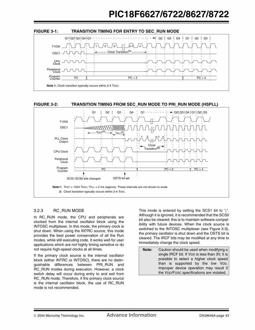
2004 Microchip Technology Inc. Advance Information DS39646A-page 43
PIC18F6627/6722/8627/8722
FIGURE 3-1: TRANSITION TIMING FOR ENTRY TO SEC_RUN MODE
FIGURE 3-2: TRANSITION TIMING FROM SEC_RUN MODE TO PRI_RUN MODE (HSPLL)
3.2.3 RC_RUN MODE
In RC_RUN mode, the CPU and peripherals areclocked from the internal oscillator block using theINTOSC multiplexer. In this mode, the primary clock isshut down. When using the INTRC source, this modeprovides the best power conservation of all the Runmodes, while still executing code. It works well for userapplications which are not highly timing sensitive or donot require high-speed clocks at all times.
If the primary clock source is the internal oscillatorblock (either INTRC or INTOSC), there are no distin-guishable differences between PRI_RUN andRC_RUN modes during execution. However, a clockswitch delay will occur during entry to and exit fromRC_RUN mode. Therefore, if the primary clock sourceis the internal oscillator block, the use of RC_RUNmode is not recommended.
This mode is entered by setting the SCS1 bit to ‘1’.Although it is ignored, it is recommended that the SCS0bit also be cleared; this is to maintain software compat-ibility with future devices. When the clock source isswitched to the INTOSC multiplexer (see Figure 3-3),the primary oscillator is shut down and the OSTS bit iscleared. The IRCF bits may be modified at any time toimmediately change the clock speed.
Q4Q3Q2
OSC1
Peripheral
Program
Q1
T1OSI
Q1
Counter
Clock
CPUClock
PC + 2PC
1 2 3 n-1 n
Clock Transition(1)
Q4Q3Q2 Q1 Q3Q2
PC + 4
Note 1: Clock transition typically occurs within 2-4 TOSC.
Q1 Q3 Q4
OSC1
Peripheral
Program PC
T1OSI
PLL Clock
Q1
PC + 4
Q2
Output
Q3 Q4 Q1
CPU Clock
PC + 2
Clock
Counter
Q2 Q2 Q3
Note1: TOST = 1024 TOSC; TPLL = 2 ms (approx). These intervals are not shown to scale.
2: Clock transition typically occurs within 2-4 TOSC.
SCS1:SCS0 bits changed
TPLL(1)
1 2 n-1 n
Clock
OSTS bit set
Transition(2)
TOST(1)
Note: Caution should be used when modifying asingle IRCF bit. If VDD is less than 3V, it ispossible to select a higher clock speedthan is supported by the low VDD.Improper device operation may result ifthe VDD/FOSC specifications are violated.

PIC18F6627/6722/8627/8722
DS39646A-page 44 Advance Information 2004 Microchip Technology Inc.
If the IRCF bits and the INTSRC bit are all clear, theINTOSC output is not enabled and the IOFS bit willremain clear; there will be no indication of the currentclock source. The INTRC source is providing thedevice clocks.
If the IRCF bits are changed from all clear (thus,enabling the INTOSC output) or if INTSRC is set, theIOFS bit becomes set after the INTOSC outputbecomes stable. Clocks to the device continue whilethe INTOSC source stabilizes after an interval ofTIOBST (parameter 39, Table 28-12).
If the IRCF bits were previously at a non-zero value, orif INTSRC was set before setting SCS1 and theINTOSC source was already stable, the IOFS bit willremain set.
On transitions from RC_RUN mode to PRI_RUN mode,the device continues to be clocked from the INTOSCmultiplexer while the primary clock is started. When theprimary clock becomes ready, a clock switch to theprimary clock occurs (see Figure 3-4). When the clockswitch is complete, the IOFS bit is cleared, the OSTSbit is set and the primary clock is providing the deviceclock. The IDLEN and SCS bits are not affected by theswitch. The INTRC source will continue to run if eitherthe WDT or the Fail-Safe Clock Monitor is enabled.
FIGURE 3-3: TRANSITION TIMING TO RC_RUN MODE
FIGURE 3-4: TRANSITION TIMING FROM RC_RUN MODE TO PRI_RUN MODE
Q4Q3Q2
OSC1
Peripheral
Program
Q1
INTRC
Q1
Counter
Clock
CPUClock
PC + 2PC
1 2 3 n-1 n
Clock Transition(1)
Q4Q3Q2 Q1 Q3Q2
PC + 4
Note 1: Clock transition typically occurs within 2-4 TOSC.
Q1 Q3 Q4
OSC1
Peripheral
Program PC
INTOSC
PLL Clock
Q1
PC + 4
Q2
Output
Q3 Q4 Q1
CPU Clock
PC + 2
Clock
Counter
Q2 Q2 Q3
Note1: TOST = 1024 TOSC; TPLL = 2 ms (approx). These intervals are not shown to scale.
2: Clock transition typically occurs within 2-4 TOSC.
SCS1:SCS0 bits changed
TPLL(1)
1 2 n-1 n
Clock
OSTS bit set
Transition(2)
Multiplexer
TOST(1)

2004 Microchip Technology Inc. Advance Information DS39646A-page 45
PIC18F6627/6722/8627/8722
3.3 Sleep Mode
The power-managed Sleep mode in the PIC18F6627/6722/8627/8722 devices is identical to the legacySleep mode offered in all other PICmicro devices. It isentered by clearing the IDLEN bit (the default state ondevice Reset) and executing the SLEEP instruction.This shuts down the selected oscillator (Figure 3-5). Allclock source status bits are cleared.
Entering the Sleep mode from any other mode does notrequire a clock switch. This is because no clocks areneeded once the controller has entered Sleep. If theWDT is selected, the INTRC source will continue tooperate. If the Timer1 oscillator is enabled, it will alsocontinue to run.
When a wake event occurs in Sleep mode (by interrupt,Reset or WDT time-out), the device will not be clockeduntil the clock source selected by the SCS1:SCS0 bitsbecomes ready (see Figure 3-6), or it will be clockedfrom the internal oscillator block if either the Two-Speed Start-up or the Fail-Safe Clock Monitor areenabled (see Section 25.0 “Special Features of theCPU”). In either case, the OSTS bit is set when theprimary clock is providing the device clocks. TheIDLEN and SCS bits are not affected by the wake-up.
3.4 Idle Modes
The Idle modes allow the controller’s CPU to beselectively shut down while the peripherals continue tooperate. Selecting a particular Idle mode allows usersto further manage power consumption.
If the IDLEN bit is set to a ‘1’ when a SLEEP instruction isexecuted, the peripherals will be clocked from the clocksource selected using the SCS1:SCS0 bits; however, theCPU will not be clocked. The clock source status bits arenot affected. Setting IDLEN and executing a SLEEPinstruction provides a quick method of switching from agiven Run mode to its corresponding Idle mode.
If the WDT is selected, the INTRC source will continueto operate. If the Timer1 oscillator is enabled, it will alsocontinue to run.
Since the CPU is not executing instructions, the onlyexits from any of the Idle modes are by interrupt, WDTtime-out or a Reset. When a wake event occurs, CPUexecution is delayed by an interval of TCSD
(parameter 38, Table 28-12) while it becomes ready toexecute code. When the CPU begins executing code,it resumes with the same clock source for the currentIdle mode. For example, when waking from RC_IDLEmode, the internal oscillator block will clock the CPUand peripherals (in other words, RC_RUN mode). TheIDLEN and SCS bits are not affected by the wake-up.
While in any Idle mode or the Sleep mode, a WDTtime-out will result in a WDT wake-up to the Run modecurrently specified by the SCS1:SCS0 bits.
FIGURE 3-5: TRANSITION TIMING FOR ENTRY TO SLEEP MODE
FIGURE 3-6: TRANSITION TIMING FOR WAKE FROM SLEEP (HSPLL)
Q4Q3Q2
OSC1
Peripheral
Sleep
Program
Q1Q1
Counter
Clock
CPUClock
PC + 2PC
Q3 Q4 Q1 Q2
OSC1
Peripheral
Program PC
PLL Clock
Q3 Q4
Output
CPU Clock
Q1 Q2 Q3 Q4 Q1 Q2
Clock
Counter PC + 6PC + 4
Q1 Q2 Q3 Q4
Wake Event
Note1: TOST = 1024 TOSC; TPLL = 2 ms (approx). These intervals are not shown to scale.
TOST(1)TPLL(1)
OSTS bit set
PC + 2

PIC18F6627/6722/8627/8722
DS39646A-page 46 Advance Information 2004 Microchip Technology Inc.
3.4.1 PRI_IDLE MODE
This mode is unique among the three low-power Idlemodes, in that it does not disable the primary deviceclock. For timing sensitive applications, this allows forthe fastest resumption of device operation with its moreaccurate primary clock source, since the clock sourcedoes not have to “warm-up” or transition from anotheroscillator.
PRI_IDLE mode is entered from PRI_RUN mode bysetting the IDLEN bit and executing a SLEEP instruc-tion. If the device is in another Run mode, set IDLENfirst, then clear the SCS bits and execute SLEEP.Although the CPU is disabled, the peripherals continueto be clocked from the primary clock source specifiedby the FOSC3:FOSC0 configuration bits. The OSTS bitremains set (see Figure 3-7).
When a wake event occurs, the CPU is clocked from theprimary clock source. A delay of interval TCSD
(parameter 39, Table 28-12) is required between thewake event and when code execution starts. This isrequired to allow the CPU to become ready to executeinstructions. After the wake-up, the OSTS bit remainsset. The IDLEN and SCS bits are not affected by thewake-up (see Figure 3-8).
3.4.2 SEC_IDLE MODE
In SEC_IDLE mode, the CPU is disabled but theperipherals continue to be clocked from the Timer1oscillator. This mode is entered from SEC_RUN by set-ting the IDLEN bit and executing a SLEEP instruction. Ifthe device is in another Run mode, set the IDLEN bitfirst, then set the SCS1:SCS0 bits to ‘01’ and executeSLEEP. When the clock source is switched to theTimer1 oscillator, the primary oscillator is shut down,the OSTS bit is cleared and the T1RUN bit is set.
When a wake event occurs, the peripherals continue tobe clocked from the Timer1 oscillator. After an intervalof TCSD following the wake event, the CPU begins exe-cuting code being clocked by the Timer1 oscillator. TheIDLEN and SCS bits are not affected by the wake-up;the Timer1 oscillator continues to run (see Figure 3-8).
FIGURE 3-7: TRANSITION TIMING FOR ENTRY TO IDLE MODE
FIGURE 3-8: TRANSITION TIMING FOR WAKE FROM IDLE TO RUN MODE
Note: The Timer1 oscillator should already berunning prior to entering SEC_IDLE mode.If the T1OSCEN bit is not set when theSLEEP instruction is executed, the SLEEPinstruction will be ignored and entry toSEC_IDLE mode will not occur. If theTimer1 oscillator is enabled but not yetrunning, peripheral clocks will be delayeduntil the oscillator has started. In such sit-uations, initial oscillator operation is farfrom stable and unpredictable operationmay result.
Q1
Peripheral
Program PC PC + 2
OSC1
Q3 Q4 Q1
CPU Clock
Clock
Counter
Q2
OSC1
Peripheral
Program PC
CPU Clock
Q1 Q3 Q4
Clock
Counter
Q2
Wake Event
TCSD

2004 Microchip Technology Inc. Advance Information DS39646A-page 47
PIC18F6627/6722/8627/8722
3.4.3 RC_IDLE MODE
In RC_IDLE mode, the CPU is disabled but the periph-erals continue to be clocked from the internal oscillatorblock using the INTOSC multiplexer. This mode allowsfor controllable power conservation during Idle periods.
From RC_RUN, this mode is entered by setting theIDLEN bit and executing a SLEEP instruction. If thedevice is in another Run mode, first set IDLEN, then setthe SCS1 bit and execute SLEEP. Although its value isignored, it is recommended that SCS0 also be cleared;this is to maintain software compatibility with futuredevices. The INTOSC multiplexer may be used toselect a higher clock frequency by modifying the IRCFbits before executing the SLEEP instruction. When theclock source is switched to the INTOSC multiplexer, theprimary oscillator is shut down and the OSTS bit iscleared.
If the IRCF bits are set to any non-zero value, or theINTSRC bit is set, the INTOSC output is enabled. TheIOFS bit becomes set, after the INTOSC outputbecomes stable, after an interval of TIOBST
(parameter 39, Table 28-12). Clocks to the peripheralscontinue while the INTOSC source stabilizes. If theIRCF bits were previously at a non-zero value, orINTSRC was set before the SLEEP instruction was exe-cuted and the INTOSC source was already stable, theIOFS bit will remain set. If the IRCF bits and INTSRCare all clear, the INTOSC output will not be enabled, theIOFS bit will remain clear and there will be no indicationof the current clock source.
When a wake event occurs, the peripherals continue tobe clocked from the INTOSC multiplexer. After a delayof TCSD (parameter 38, Table 28-12) following the wakeevent, the CPU begins executing code being clockedby the INTOSC multiplexer. The IDLEN and SCS bitsare not affected by the wake-up. The INTRC source willcontinue to run if either the WDT or the Fail-Safe ClockMonitor is enabled.
3.5 Exiting Idle and Sleep Modes
An exit from Sleep mode or any of the Idle modes istriggered by an interrupt, a Reset or a WDT time-out.This section discusses the triggers that cause exitsfrom power-managed modes. The clocking subsystemactions are discussed in each of the power-managedmodes (see Section 3.2 “Run Modes”, Section 3.3“Sleep Mode” and Section 3.4 “Idle Modes”).
3.5.1 EXIT BY INTERRUPT
Any of the available interrupt sources can cause thedevice to exit from an Idle mode or the Sleep mode toa Run mode. To enable this functionality, an interruptsource must be enabled by setting its enable bit in oneof the INTCON or PIE registers. The exit sequence isinitiated when the corresponding interrupt flag bit is set.
On all exits from Idle or Sleep modes by interrupt, codeexecution branches to the interrupt vector if the GIE/GIEH bit (INTCON<7>) is set. Otherwise, code execu-tion continues or resumes without branching (seeSection 10.0 “Interrupts”).
A fixed delay of interval TCSD following the wake eventis required when leaving Sleep and Idle modes. Thisdelay is required for the CPU to prepare for execution.Instruction execution resumes on the first clock cyclefollowing this delay.
3.5.2 EXIT BY WDT TIME-OUT
A WDT time-out will cause different actions dependingon which power-managed mode the device is in whenthe time-out occurs.
If the device is not executing code (all Idle modes andSleep mode), the time-out will result in an exit from thepower-managed mode (see Section 3.2 “RunModes” and Section 3.3 “Sleep Mode”). If the deviceis executing code (all Run modes), the time-out willresult in a WDT Reset (see Section 25.2 “WatchdogTimer (WDT)”).
The WDT timer and postscaler are cleared byexecuting a SLEEP or CLRWDT instruction, the loss of acurrently selected clock source (if the Fail-Safe ClockMonitor is enabled) and modifying the IRCF bits in theOSCCON register if the internal oscillator block is thedevice clock source.
3.5.3 EXIT BY RESET
Normally, the device is held in Reset by the OscillatorStart-up Timer (OST) until the primary clock becomesready. At that time, the OSTS bit is set and the devicebegins executing code. If the internal oscillator block isthe new clock source, the IOFS bit is set instead.
The exit delay time from Reset to the start of codeexecution depends on both the clock sources beforeand after the wake-up and the type of oscillator if thenew clock source is the primary clock. Exit delays aresummarized in Table 3-2.
Code execution can begin before the primary clockbecomes ready. If either the Two-Speed Start-up (seeSection 25.3 “Two-Speed Start-up”) or Fail-SafeClock Monitor (see Section 25.4 “Fail-Safe ClockMonitor”) is enabled, the device may begin executionas soon as the Reset source has cleared. Execution isclocked by the INTOSC multiplexer driven by the inter-nal oscillator block. Execution is clocked by the internaloscillator block until either the primary clock becomesready or a power-managed mode is entered before theprimary clock becomes ready; the primary clock is thenshut down.

PIC18F6627/6722/8627/8722
DS39646A-page 48 Advance Information 2004 Microchip Technology Inc.
3.5.4 EXIT WITHOUT AN OSCILLATOR START-UP DELAY
Certain exits from power-managed modes do notinvoke the OST at all. There are two cases:
• PRI_IDLE mode, where the primary clock source is not stopped and
• the primary clock source is not any of the LP, XT, HS or HSPLL modes.
In these instances, the primary clock source eitherdoes not require an oscillator start-up delay since it isalready running (PRI_IDLE), or normally does notrequire an oscillator start-up delay (RC, EC and INTIOOscillator modes). However, a fixed delay of intervalTCSD following the wake event is still required whenleaving Sleep and Idle modes to allow the CPU toprepare for execution. Instruction execution resumeson the first clock cycle following this delay.
TABLE 3-2: EXIT DELAY ON WAKE-UP BY RESET FROM SLEEP MODE OR ANY IDLE MODE(BY CLOCK SOURCES)
Clock Sourcebefore Wake-up
Clock Source after Wake-up
Exit DelayClock Ready Status
Bit (OSCCON)
Primary Device Clock(PRI_IDLE mode)
LP, XT, HS
TCSD(1) OSTSHSPLL
EC, RC
INTOSC(2) IOFS
T1OSC or INTRC(1)
LP, XT, HS TOST(3)
OSTSHSPLL TOST + trc(3)
EC, RC TCSD(1)
INTOSC(1) TIOBST(4) IOFS
INTOSC(2)
LP, XT, HS TOST(4)
OSTSHSPLL TOST + trc(3)
EC, RC TCSD(1)
INTOSC(1) None IOFS
None(Sleep mode)
LP, XT, HS TOST(3)
OSTSHSPLL TOST + trc(3)
EC, RC TCSD(1)
INTOSC(1) TIOBST(4) IOFS
Note 1: TCSD (parameter 38, Table 28-12) is a required delay when waking from Sleep and all Idle modes and runs concurrently with any other required delays (see Section 3.4 “Idle Modes”). On Reset, INTOSC defaults to 1 MHz.
2: Includes both the INTOSC 8 MHz source and postscaler derived frequencies.3: TOST is the Oscillator Start-up Timer (parameter 32, Table 28-12). trc is the PLL Lock-out Timer
(parameter F12, Table 28-7); it is also designated as TPLL.4: Execution continues during TIOBST (parameter 39, Table 28-12), the INTOSC stabilization period.

2004 Microchip Technology Inc. Advance Information DS39646A-page 49
PIC18F6627/6722/8627/8722
4.0 RESET
The PIC18F6627/6722/8627/8722 devices differentiatebetween various kinds of Reset:
a) Power-on Reset (POR)
b) MCLR Reset during normal operationc) MCLR Reset during power-managed modes d) Watchdog Timer (WDT) Reset (during
execution)e) Programmable Brown-out Reset (BOR)
f) RESET Instructiong) Stack Full Reseth) Stack Underflow Reset
This section discusses Resets generated by MCLR,POR and BOR and covers the operation of the variousstart-up timers. Stack Reset events are covered inSection 5.1.3.4 “Stack Full and Underflow Resets”.WDT Resets are covered in Section 25.2 “WatchdogTimer (WDT)”.
A simplified block diagram of the On-Chip Reset Circuitis shown in Figure 4-1.
4.1 RCON Register
Device Reset events are tracked through the RCONregister (Register 4-1). The lower five bits of the regis-ter indicate that a specific Reset event has occurred. Inmost cases, these bits can only be cleared by the eventand must be set by the application after the event. Thestate of these flag bits, taken together, can be read toindicate the type of Reset that just occurred. This isdescribed in more detail in Section 4.6 “Reset Stateof Registers”.
The RCON register also has control bits for settinginterrupt priority (IPEN) and software control of theBOR (SBOREN). Interrupt priority is discussed inSection 10.0 “Interrupts”. BOR is covered inSection 4.4 “Brown-out Reset (BOR)”.
FIGURE 4-1: SIMPLIFIED BLOCK DIAGRAM OF ON-CHIP RESET CIRCUIT
External Reset
MCLR
VDD
OSC1
WDTTime-out
VDD RiseDetect
OST/PWRT
INTRC(1)
POR Pulse
OST
10-bit Ripple Counter
PWRT
11-bit Ripple Counter
Enable OST(2)
Enable PWRT
Note 1: This is the INTRC source from the internal oscillator block and is separate from the RC oscillator of the CLKI pin.
2: See Table 4-2 for time-out situations.
Brown-outReset
BOREN
RESETInstruction
StackPointer
Stack Full/Underflow Reset
Sleep( )_IDLE
1024 Cycles
64 ms32 µs
MCLRE
S
R QChip_Reset

PIC18F6627/6722/8627/8722
DS39646A-page 50 Advance Information 2004 Microchip Technology Inc.
REGISTER 4-1: RCON: RESET CONTROL REGISTER R/W-0 R/W-1(1) U-0 R/W-1 R-1 R-1 R/W-0(2) R/W-0
IPEN SBOREN — RI TO PD POR BOR
bit 7 bit 0
bit 7 IPEN: Interrupt Priority Enable bit 1 = Enable priority levels on interrupts0 = Disable priority levels on interrupts (PIC16CXXX Compatibility mode)
bit 6 SBOREN: BOR Software Enable bit(1) If BOREN1:BOREN0 = 01:1 = BOR is enabled0 = BOR is disabled
If BOREN1:BOREN0 = 00, 10 or 11:Bit is disabled and read as ‘0’.
bit 5 Unimplemented: Read as ‘0’
bit 4 RI: RESET Instruction Flag bit1 = The RESET instruction was not executed (set by firmware only)0 = The RESET instruction was executed causing a device Reset (must be set in software after
a Brown-out Reset occurs)
bit 3 TO: Watchdog Time-out Flag bit 1 = Set by power-up, CLRWDT instruction or SLEEP instruction 0 = A WDT time-out occurred
bit 2 PD: Power-down Detection Flag bit 1 = Set by power-up or by the CLRWDT instruction 0 = Set by execution of the SLEEP instruction
bit 1 POR: Power-on Reset Status bit(2)
1 = A Power-on Reset has not occurred (set by firmware only)0 = A Power-on Reset occurred (must be set in software after a Power-on Reset occurs)
bit 0 BOR: Brown-out Reset Status bit1 = A Brown-out Reset has not occurred (set by firmware only)0 = A Brown-out Reset occurred (must be set in software after a Brown-out Reset occurs)
Note 1: If SBOREN is enabled, its Reset state is ‘1’; otherwise, it is ‘0’.
2: The actual Reset value of POR is determined by the type of device Reset. See thenotes following this register and Section 4.6 “Reset State of Registers” foradditional information.
Legend:
R = Readable bit W = Writable bit U = Unimplemented bit, read as ‘0’
-n = Value at POR ‘1’ = Bit is set ‘0’ = Bit is cleared x = Bit is unknown
Note 1: It is recommended that the POR bit be set after a Power-on Reset has beendetected so that subsequent Power-on Resets may be detected.
2: Brown-out Reset is said to have occurred when BOR is ‘0’ and POR is ‘1’ (assumingthat POR was set to ‘1’ by software immediately after POR).

2004 Microchip Technology Inc. Advance Information DS39646A-page 51
PIC18F6627/6722/8627/8722
4.2 Master Clear (MCLR)
The MCLR pin provides a method for triggering anexternal Reset of the device. A Reset is generated byholding the pin low. These devices have a noise filter inthe MCLR Reset path which detects and ignores smallpulses.
The MCLR pin is not driven low by any internal Resets,including the WDT.
In PIC18F6627/6722/8627/8722 devices, the MCLRinput can be disabled with the MCLRE configuration bit.When MCLR is disabled, the pin becomes a digitalinput. See Section 11.5 “PORTE, TRISE and LATERegisters” for more information.
4.3 Power-on Reset (POR)
A Power-on Reset pulse is generated on-chipwhenever VDD rises above a certain threshold. Thisallows the device to start in the initialized state whenVDD is adequate for operation.
To take advantage of the POR circuitry, tie the MCLRpin through a resistor (1 kΩ to 10 kΩ) to VDD. This willeliminate external RC components usually needed tocreate a Power-on Reset delay. A minimum rise rate forVDD is specified (parameter D004, Section 28.1 “DCCharacteristics”). For a slow rise time, see Figure 4-2.
When the device starts normal operation (i.e., exits theReset condition), device operating parameters (volt-age, frequency, temperature, etc.) must be met toensure operation. If these conditions are not met, thedevice must be held in Reset until the operatingconditions are met.
POR events are captured by the POR bit (RCON<1>).The state of the bit is set to ‘0’ whenever a POR occurs;it does not change for any other Reset event. POR isnot reset to ‘1’ by any hardware event. To capturemultiple events, the user manually resets the bit to ‘1’in software following any POR.
FIGURE 4-2: EXTERNAL POWER-ON RESET CIRCUIT (FOR SLOW VDD POWER-UP)(1)
Note 1: External Power-on Reset circuit is requiredonly if the VDD power-up slope is too slow.The diode D helps discharge the capacitorquickly when VDD powers down.
2: R < 40 kΩ is recommended to make sure thatthe voltage drop across R does not violatethe device’s electrical specification.
3: R1 ≥ 1 kΩ will limit any current flowing intoMCLR from external capacitor C, in the eventof MCLR/VPP pin breakdown, due toElectrostatic Discharge (ESD) or ElectricalOverstress (EOS).
C
R1(3)R(2)D
VDD
MCLR
PIC18FXXXX
VDD

PIC18F6627/6722/8627/8722
DS39646A-page 52 Advance Information 2004 Microchip Technology Inc.
4.4 Brown-out Reset (BOR)
PIC18F6627/6722/8627/8722 devices implement aBOR circuit that provides the user with a number ofconfiguration and power-saving options. The BOR iscontrolled by the BORV1:BORV0 andBOREN1:BOREN0 configuration bits. There are a totalof four BOR configurations which are summarized inTable 4-1.
The BOR threshold is set by the BORV1:BORV0 bits. IfBOR is enabled (any values of BOREN1:BOREN0,except ‘00’), any drop of VDD below VBOR (parameterD005, Section 28.1 “DC Characteristics”) for greaterthan TBOR (parameter 35, Table 28-12) will reset thedevice. A Reset may or may not occur if VDD falls belowVBOR for less than TBOR. The chip will remain in Brown-out Reset until VDD rises above VBOR.
If the Power-up Timer is enabled, it will be invoked afterVDD rises above VBOR; it then will keep the chip inReset for an additional time delay, TPWRT(parameter 33, Table 28-12). If VDD drops below VBOR
while the Power-up Timer is running, the chip will goback into a Brown-out Reset and the Power-up Timerwill be initialized. Once VDD rises above VBOR, thePower-up Timer will execute the additional time delay.
BOR and the Power-on Timer (PWRT) areindependently configured. Enabling BOR Reset doesnot automatically enable the PWRT.
4.4.1 SOFTWARE ENABLED BOR
When BOREN1:BOREN0 = 01, the BOR can beenabled or disabled by the user in software. This isdone with the control bit, SBOREN (RCON<6>).Setting SBOREN enables the BOR to function aspreviously described. Clearing SBOREN disables theBOR entirely. The SBOREN bit operates only in thismode; otherwise it is read as ‘0’.
Placing the BOR under software control gives the userthe additional flexibility of tailoring the application to itsenvironment without having to reprogram the device tochange the BOR configuration. It also allows the userto tailor device power consumption in software by elim-inating the incremental current that the BOR con-sumes. While the BOR current is typically very small, itmay have some impact in low-power applications.
4.4.2 DETECTING BOR
When BOR is enabled, the BOR bit always resets to ‘0’on any BOR or POR event. This makes it difficult todetermine if a BOR event has occurred just by readingthe state of BOR alone. A more reliable method is tosimultaneously check the state of both POR and BOR.This assumes that the POR bit is reset to ‘1’ in softwareimmediately after any POR event. If BOR is ‘0’ whilePOR is ‘1’, it can be reliably assumed that a BOR eventhas occurred.
4.4.3 DISABLING BOR IN SLEEP MODE
When BOREN1:BOREN0 = 10, the BOR remainsunder hardware control and operates as previouslydescribed. Whenever the device enters Sleep mode,however, the BOR is automatically disabled. When thedevice returns to any other operating mode, BOR isautomatically re-enabled.
This mode allows for applications to recover frombrown-out situations, while actively executing code,when the device requires BOR protection the most. Atthe same time, it saves additional power in Sleep modeby eliminating the small incremental BOR current.
TABLE 4-1: BOR CONFIGURATIONS
Note: Even when BOR is under software control,the BOR Reset voltage level is still set bythe BORV1:BORV0 configuration bits. Itcannot be changed in software.
BOR Configuration Status of SBOREN
(RCON<6>)BOR Operation
BOREN1 BOREN0
0 0 Unavailable BOR disabled; must be enabled by reprogramming the configuration bits.
0 1 Available BOR enabled in software; operation controlled by SBOREN.
1 0 Unavailable BOR enabled in hardware in Run and Idle modes, disabled during Sleep mode.
1 1 Unavailable BOR enabled in hardware; must be disabled by reprogramming the configuration bits.

2004 Microchip Technology Inc. Advance Information DS39646A-page 53
PIC18F6627/6722/8627/8722
4.5 Device Reset Timers
PIC18F6627/6722/8627/8722 devices incorporate threeseparate on-chip timers that help regulate the Power-onReset process. Their main function is to ensure that thedevice clock is stable before code is executed. Thesetimers are:
• Power-up Timer (PWRT)• Oscillator Start-up Timer (OST)
• PLL Lock Time-out
4.5.1 POWER-UP TIMER (PWRT)
The Power-up Timer (PWRT) of PIC18F6627/6722/8627/8722 devices is an 11-bit counter which usesthe INTRC source as the clock input. While thePWRT is counting, the device is held in Reset.
The power-up time delay depends on the INTRC clockand will vary from chip-to-chip due to temperature andprocess variation. See DC parameter 33 in Table 28-12for details.
The PWRT is enabled by clearing the PWRTENconfiguration bit.
4.5.2 OSCILLATOR START-UP TIMER (OST)
The Oscillator Start-up Timer (OST) provides a 1024oscillator cycle (from OSC1 input) delay after thePWRT delay is over (parameter 33, Table 28-12). Thisensures that the crystal oscillator or resonator hasstarted and stabilized.
The OST time-out is invoked only for XT, LP, HS andHSPLL modes and only on Power-on Reset, or on exitfrom most power-managed modes.
4.5.3 PLL LOCK TIME-OUT
With the PLL enabled in its PLL mode, the time-outsequence following a Power-on Reset is slightly differ-ent from other oscillator modes. A separate timer isused to provide a fixed time-out that is sufficient for thePLL to lock to the main oscillator frequency. This PLLlock time-out (TPLL) is typically 2 ms and follows theoscillator start-up time-out.
4.5.4 TIME-OUT SEQUENCE
On power-up, the time-out sequence is as follows:
1. After the POR pulse has cleared, PWRT time-outis invoked (if enabled).
2. Then, the OST is activated.
The total time-out will vary based on oscillator configu-ration and the status of the PWRT. Figure 4-3,Figure 4-4, Figure 4-5, Figure 4-6 and Figure 4-7 alldepict time-out sequences on power-up, with thePower-up Timer enabled and the device operating inHS Oscillator mode. Figures 4-3 through 4-6 alsoapply to devices operating in XT or LP modes. Fordevices in RC mode and with the PWRT disabled, onthe other hand, there will be no time-out at all.
Since the time-outs occur from the POR pulse, if MCLRis kept low long enough, all time-outs will expire. Bring-ing MCLR high will begin execution immediately(Figure 4-5). This is useful for testing purposes or tosynchronize more than one PIC18FXXXX deviceoperating in parallel.
TABLE 4-2: TIME-OUT IN VARIOUS SITUATIONS
OscillatorConfiguration
Power-up(2) and Brown-out Exit from Power-Managed ModePWRTEN = 0 PWRTEN = 1
HSPLL TPWRT(1) + 1024 TOSC + 2 ms(2) 1024 TOSC + 2 ms(2) 1024 TOSC + 2 ms(2)
HS, XT, LP TPWRT(1) + 1024 TOSC 1024 TOSC 1024 TOSC
EC, ECIO TPWRT(1) — —
RC, RCIO TPWRT(1) — —
INTIO1, INTIO2 TPWRT(1) — —
Note 1: See parameter 33, Table 28-12.2: 2 ms is the nominal time required for the PLL to lock.

PIC18F6627/6722/8627/8722
DS39646A-page 54 Advance Information 2004 Microchip Technology Inc.
FIGURE 4-3: TIME-OUT SEQUENCE ON POWER-UP (MCLR TIED TO VDD, VDD RISE < TPWRT)
FIGURE 4-4: TIME-OUT SEQUENCE ON POWER-UP (MCLR NOT TIED TO VDD): CASE 1
FIGURE 4-5: TIME-OUT SEQUENCE ON POWER-UP (MCLR NOT TIED TO VDD): CASE 2
TPWRT
TOST
VDD
MCLR
INTERNAL POR
PWRT TIME-OUT
OST TIME-OUT
INTERNAL RESET
TPWRT
TOST
VDD
MCLR
INTERNAL POR
PWRT TIME-OUT
OST TIME-OUT
INTERNAL RESET
VDD
MCLR
INTERNAL POR
PWRT TIME-OUT
OST TIME-OUT
INTERNAL RESET
TPWRT
TOST

2004 Microchip Technology Inc. Advance Information DS39646A-page 55
PIC18F6627/6722/8627/8722
FIGURE 4-6: SLOW RISE TIME (MCLR TIED TO VDD, VDD RISE > TPWRT)
FIGURE 4-7: TIME-OUT SEQUENCE ON POR W/PLL ENABLED (MCLR TIED TO VDD)
VDD
MCLR
INTERNAL POR
PWRT TIME-OUT
OST TIME-OUT
INTERNAL RESET
TPWRT
TOST
TPWRT
TOST
VDD
MCLR
INTERNAL POR
PWRT TIME-OUT
OST TIME-OUT
INTERNAL RESET
PLL TIME-OUT
TPLL
Note: TOST = 1024 clock cycles.TPLL ≈ See parameter 33 in Table 28-12.

PIC18F6627/6722/8627/8722
DS39646A-page 56 Advance Information 2004 Microchip Technology Inc.
4.6 Reset State of Registers
Most registers are unaffected by a Reset. Their statusis unknown on POR and unchanged by all otherResets. All other registers are forced to a “Reset state”depending on the type of Reset that occurred.
Most registers are not affected by a WDT wake-up,since this is viewed as the resumption of normal oper-ation. Status bits from the RCON register, RI, TO, PD,POR and BOR, are set or cleared differently in differentReset situations, as indicated in Table 4-3. These bitsare used in software to determine the nature of theReset.
Table 4-4 describes the Reset states for all of theSpecial Function Registers. These are categorized byPower-on and Brown-out Resets, Master Clear andWDT Resets and WDT wake-ups.
TABLE 4-3: STATUS BITS, THEIR SIGNIFICANCE AND THE INITIALIZATION CONDITION FOR RCON REGISTER
ConditionProgram Counter
RCON Register STKPTR Register
SBOREN RI TO PD POR BOR STKFUL STKUNF
Power-on Reset 0000h 1 1 1 1 0 0 0 0
RESET Instruction 0000h u(2) 0 u u u u u u
Brown-out Reset 0000h u(2) 1 1 1 u 0 u u
MCLR during Power-Managed Run Modes
0000h u(2) u 1 u u u u u
MCLR during Power-Managed Idle Modes and Sleep Mode
0000h u(2) u 1 0 u u u u
WDT Time-out during Full Power or Power-Managed Run Mode
0000h u(2) u 0 u u u u u
MCLR during Full Power Execution
0000h u(2) u u u u u u u
Stack Full Reset (STVREN = 1) 0000h u(2) u u u u u 1 u
Stack Underflow Reset (STVREN = 1)
0000h u(2) u u u u u u 1
Stack Underflow Error (not an actual Reset, STVREN = 0)
0000h u(2) u u u u u u 1
WDT Time-out during Power-Managed Idle or Sleep Modes
PC + 2 u(2) u 0 0 u u u u
Interrupt Exit from Power-Managed Modes
PC + 2(1) u(2) u u 0 u u u u
Legend: u = unchanged
Note 1: When the wake-up is due to an interrupt and the GIEH or GIEL bits are set, the PC is loaded with the interrupt vector (008h or 0018h).
2: Reset state is ‘1’ for POR and unchanged for all other Resets when software BOR is enabled (BOREN1:BOREN0 configuration bits = 01 and SBOREN = 1). Otherwise, the Reset state is ‘0’.

2004 Microchip Technology Inc. Advance Information DS39646A-page 57
PIC18F6627/6722/8627/8722 TABLE 4-4: INITIALIZATION CONDITIONS FOR ALL REGISTERS
Register Applicable DevicesPower-on Reset,Brown-out Reset
MCLR Resets,WDT Reset,
RESET Instruction,Stack Resets
Wake-up via WDT or Interrupt
TOSU 6627 6722 8627 8722 ---0 0000 ---0 0000 ---0 uuuu(3)
TOSH 6627 6722 8627 8722 0000 0000 0000 0000 uuuu uuuu(3)
TOSL 6627 6722 8627 8722 0000 0000 0000 0000 uuuu uuuu(3)
STKPTR 6627 6722 8627 8722 00-0 0000 uu-u uuuu uu-u uuuu(3)
PCLATU 6627 6722 8627 8722 ---0 0000 ---0 0000 ---u uuuu
PCLATH 6627 6722 8627 8722 0000 0000 0000 0000 uuuu uuuu
PCL 6627 6722 8627 8722 0000 0000 0000 0000 PC + 2(2)
TBLPTRU 6627 6722 8627 8722 --00 0000 --00 0000 --uu uuuu
TBLPTRH 6627 6722 8627 8722 0000 0000 0000 0000 uuuu uuuu
TBLPTRL 6627 6722 8627 8722 0000 0000 0000 0000 uuuu uuuu
TABLAT 6627 6722 8627 8722 0000 0000 0000 0000 uuuu uuuu
PRODH 6627 6722 8627 8722 xxxx xxxx uuuu uuuu uuuu uuuu
PRODL 6627 6722 8627 8722 xxxx xxxx uuuu uuuu uuuu uuuu
INTCON 6627 6722 8627 8722 0000 000x 0000 000u uuuu uuuu(1)
INTCON2 6627 6722 8627 8722 1111 1111 1111 1111 uuuu uuuu(1)
INTCON3 6627 6722 8627 8722 1100 0000 1100 0000 uuuu uuuu(1)
INDF0 6627 6722 8627 8722 N/A N/A N/A
POSTINC0 6627 6722 8627 8722 N/A N/A N/A
POSTDEC0 6627 6722 8627 8722 N/A N/A N/A
PREINC0 6627 6722 8627 8722 N/A N/A N/A
PLUSW0 6627 6722 8627 8722 N/A N/A N/A
FSR0H 6627 6722 8627 8722 ---- 0000 ---- 0000 ---- uuuu
FSR0L 6627 6722 8627 8722 xxxx xxxx uuuu uuuu uuuu uuuu
WREG 6627 6722 8627 8722 xxxx xxxx uuuu uuuu uuuu uuuu
INDF1 6627 6722 8627 8722 N/A N/A N/A
POSTINC1 6627 6722 8627 8722 N/A N/A N/A
POSTDEC1 6627 6722 8627 8722 N/A N/A N/A
PREINC1 6627 6722 8627 8722 N/A N/A N/A
PLUSW1 6627 6722 8627 8722 N/A N/A N/A
Legend: u = unchanged, x = unknown, - = unimplemented bit, read as ‘0’, q = value depends on condition.Shaded cells indicate conditions do not apply for the designated device.
Note 1: One or more bits in the INTCONx or PIRx registers will be affected (to cause wake-up).2: When the wake-up is due to an interrupt and the GIEL or GIEH bit is set, the PC is loaded with the interrupt vector
(0008h or 0018h).3: When the wake-up is due to an interrupt and the GIEL or GIEH bit is set, the TOSU, TOSH and TOSL are updated with
the current value of the PC. The STKPTR is modified to point to the next location in the hardware stack.4: See Table 4-3 for Reset value for specific condition.5: Bits 6 and 7 of PORTA, LATA and TRISA are enabled, depending on the oscillator mode selected. When not enabled
as PORTA pins, they are disabled and read ‘0’.

PIC18F6627/6722/8627/8722
DS39646A-page 58 Advance Information 2004 Microchip Technology Inc.
FSR1H 6627 6722 8627 8722 ---- 0000 ---- 0000 ---- uuuu
FSR1L 6627 6722 8627 8722 xxxx xxxx uuuu uuuu uuuu uuuu
BSR 6627 6722 8627 8722 ---- 0000 ---- 0000 ---- uuuu
INDF2 6627 6722 8627 8722 N/A N/A N/A
POSTINC2 6627 6722 8627 8722 N/A N/A N/A
POSTDEC2 6627 6722 8627 8722 N/A N/A N/A
PREINC2 6627 6722 8627 8722 N/A N/A N/A
PLUSW2 6627 6722 8627 8722 N/A N/A N/A
FSR2H 6627 6722 8627 8722 ---- 0000 ---- 0000 ---- uuuu
FSR2L 6627 6722 8627 8722 xxxx xxxx uuuu uuuu uuuu uuuu
STATUS 6627 6722 8627 8722 ---x xxxx ---u uuuu ---u uuuu
TMR0H 6627 6722 8627 8722 0000 0000 0000 0000 uuuu uuuu
TMR0L 6627 6722 8627 8722 xxxx xxxx uuuu uuuu uuuu uuuu
T0CON 6627 6722 8627 8722 1111 1111 1111 1111 uuuu uuuu
OSCCON 6627 6722 8627 8722 0100 q000 0100 q000 uuuu uuqu
HLVDCON 6627 6722 8627 8722 0-00 0101 0-00 0101 u-uu uuuu
WDTCON 6627 6722 8627 8722 ---- ---0 ---- ---0 ---- ---u
RCON(4) 6627 6722 8627 8722 0q-1 11q0 0q-q qquu uq-u qquu
TMR1H 6627 6722 8627 8722 xxxx xxxx uuuu uuuu uuuu uuuu
TMR1L 6627 6722 8627 8722 xxxx xxxx uuuu uuuu uuuu uuuu
T1CON 6627 6722 8627 8722 0000 0000 u0uu uuuu uuuu uuuu
TMR2 6627 6722 8627 8722 0000 0000 0000 0000 uuuu uuuu
PR2 6627 6722 8627 8722 1111 1111 uuuu uuuu uuuu uuuu
T2CON 6627 6722 8627 8722 -000 0000 -000 0000 -uuu uuuu
SSP1BUF 6627 6722 8627 8722 xxxx xxxx uuuu uuuu uuuu uuuu
SSP1ADD 6627 6722 8627 8722 0000 0000 0000 0000 uuuu uuuu
SSP1STAT 6627 6722 8627 8722 0000 0000 0000 0000 uuuu uuuu
SSP1CON1 6627 6722 8627 8722 0000 0000 0000 0000 uuuu uuuu
SSP1CON2 6627 6722 8627 8722 0000 0000 0000 0000 uuuu uuuu
TABLE 4-4: INITIALIZATION CONDITIONS FOR ALL REGISTERS (CONTINUED)
Register Applicable DevicesPower-on Reset,Brown-out Reset
MCLR Resets,WDT Reset,
RESET Instruction,Stack Resets
Wake-up via WDT or Interrupt
Legend: u = unchanged, x = unknown, - = unimplemented bit, read as ‘0’, q = value depends on condition.Shaded cells indicate conditions do not apply for the designated device.
Note 1: One or more bits in the INTCONx or PIRx registers will be affected (to cause wake-up).2: When the wake-up is due to an interrupt and the GIEL or GIEH bit is set, the PC is loaded with the interrupt vector
(0008h or 0018h).3: When the wake-up is due to an interrupt and the GIEL or GIEH bit is set, the TOSU, TOSH and TOSL are updated with
the current value of the PC. The STKPTR is modified to point to the next location in the hardware stack.4: See Table 4-3 for Reset value for specific condition.5: Bits 6 and 7 of PORTA, LATA and TRISA are enabled, depending on the oscillator mode selected. When not enabled
as PORTA pins, they are disabled and read ‘0’.

2004 Microchip Technology Inc. Advance Information DS39646A-page 59
PIC18F6627/6722/8627/8722
ADRESH 6627 6722 8627 8722 xxxx xxxx uuuu uuuu uuuu uuuu
ADRESL 6627 6722 8627 8722 xxxx xxxx uuuu uuuu uuuu uuuu
ADCON0 6627 6722 8627 8722 --00 0000 --00 0000 --uu uuuu
ADCON1 6627 6722 8627 8722 --00 0000 --00 0000 --uu uuuu
ADCON2 6627 6722 8627 8722 0-00 0000 0-00 0000 u-uu uuuu
CCPR1H 6627 6722 8627 8722 xxxx xxxx uuuu uuuu uuuu uuuu
CCPR1L 6627 6722 8627 8722 xxxx xxxx uuuu uuuu uuuu uuuu
CCP1CON 6627 6722 8627 8722 0000 0000 0000 0000 uuuu uuuu
CCPR2H 6627 6722 8627 8722 xxxx xxxx uuuu uuuu uuuu uuuu
CCPR2L 6627 6722 8627 8722 xxxx xxxx uuuu uuuu uuuu uuuu
CCP2CON 6627 6722 8627 8722 0000 0000 0000 0000 uuuu uuuu
CCPR3H 6627 6722 8627 8722 xxxx xxxx uuuu uuuu uuuu uuuu
CCPR3L 6627 6722 8627 8722 xxxx xxxx uuuu uuuu uuuu uuuu
CCP3CON 6627 6722 8627 8722 0000 0000 0000 0000 uuuu uuuu
ECCP1AS 6627 6722 8627 8722 0000 0000 0000 0000 uuuu uuuu
CVRCON 6627 6722 8627 8722 0000 0000 0000 0000 uuuu uuuu
CMCON 6627 6722 8627 8722 0000 0000 0000 0000 uuuu uuuu
TMR3H 6627 6722 8627 8722 xxxx xxxx uuuu uuuu uuuu uuuu
TMR3L 6627 6722 8627 8722 xxxx xxxx uuuu uuuu uuuu uuuu
T3CON 6627 6722 8627 8722 0000 0000 uuuu uuuu uuuu uuuu
PSPCON 6627 6722 8627 8722 0000 ---- 0000 ---- uuuu ----
SPBRG1 6627 6722 8627 8722 0000 0000 0000 0000 uuuu uuuu
RCREG1 6627 6722 8627 8722 0000 0000 0000 0000 uuuu uuuu
TXREG1 6627 6722 8627 8722 0000 0000 0000 0000 uuuu uuuu
TXSTA1 6627 6722 8627 8722 0000 0010 0000 0010 uuuu uuuu
RCSTA1 6627 6722 8627 8722 0000 000x 0000 000x uuuu uuuu
EEADRH 6627 6722 8627 8722 ---- --00 ---- --00 ---- --uu
EEADR 6627 6722 8627 8722 0000 0000 0000 0000 uuuu uuuu
EEDATA 6627 6722 8627 8722 0000 0000 0000 0000 uuuu uuuu
EECON2 6627 6722 8627 8722 0000 0000 0000 0000 0000 0000
EECON1 6627 6722 8627 8722 xx-0 x000 uu-0 u000 uu-u uuuu
TABLE 4-4: INITIALIZATION CONDITIONS FOR ALL REGISTERS (CONTINUED)
Register Applicable DevicesPower-on Reset,Brown-out Reset
MCLR Resets,WDT Reset,
RESET Instruction,Stack Resets
Wake-up via WDT or Interrupt
Legend: u = unchanged, x = unknown, - = unimplemented bit, read as ‘0’, q = value depends on condition.Shaded cells indicate conditions do not apply for the designated device.
Note 1: One or more bits in the INTCONx or PIRx registers will be affected (to cause wake-up).2: When the wake-up is due to an interrupt and the GIEL or GIEH bit is set, the PC is loaded with the interrupt vector
(0008h or 0018h).3: When the wake-up is due to an interrupt and the GIEL or GIEH bit is set, the TOSU, TOSH and TOSL are updated with
the current value of the PC. The STKPTR is modified to point to the next location in the hardware stack.4: See Table 4-3 for Reset value for specific condition.5: Bits 6 and 7 of PORTA, LATA and TRISA are enabled, depending on the oscillator mode selected. When not enabled
as PORTA pins, they are disabled and read ‘0’.

PIC18F6627/6722/8627/8722
DS39646A-page 60 Advance Information 2004 Microchip Technology Inc.
IPR3 6627 6722 8627 8722 1111 1111 1111 1111 uuuu uuuu
PIR3 6627 6722 8627 8722 0000 0000 0000 0000 uuuu uuuu(1)
PIE3 6627 6722 8627 8722 0000 0000 0000 0000 uuuu uuuu
IPR2 6627 6722 8627 8722 11-1 1111 11-1 1111 uu-u uuuu
PIR2 6627 6722 8627 8722 00-0 0000 00-0 0000 uu-u uuuu(1)
PIE2 6627 6722 8627 8722 00-0 0000 00-0 0000 uu-u uuuu
IPR1 6627 6722 8627 8722 1111 1111 1111 1111 uuuu uuuu
PIR1 6627 6722 8627 8722 0000 0000 0000 0000 uuuu uuuu(1)
PIE1 6627 6722 8627 8722 0000 0000 0000 0000 uuuu uuuu
MEMCON 6627 6722 8627 8722 0-00 --00 0-00 --00 u-uu --uu
OSCTUNE 6627 6722 8627 8722 00-0 0000 00-0 0000 uu-u uuuu
TRISJ 6627 6722 8627 8722 1111 1111 1111 1111 uuuu uuuu
TRISH 6627 6722 8627 8722 1111 1111 1111 1111 uuuu uuuu
TRISG 6627 6722 8627 8722 ---1 1111 ---1 1111 ---u uuuu
TRISF 6627 6722 8627 8722 1111 1111 1111 1111 uuuu uuuu
TRISE 6627 6722 8627 8722 1111 1111 1111 1111 uuuu uuuu
TRISD 6627 6722 8627 8722 1111 1111 1111 1111 uuuu uuuu
TRISC 6627 6722 8627 8722 1111 1111 1111 1111 uuuu uuuu
TRISB 6627 6722 8627 8722 1111 1111 1111 1111 uuuu uuuu
TRISA(5) 6627 6722 8627 8722 1111 1111(5) 1111 1111(5) uuuu uuuu(5)
LATJ 6627 6722 8627 8722 xxxx xxxx uuuu uuuu uuuu uuuu
LATH 6627 6722 8627 8722 xxxx xxxx uuuu uuuu uuuu uuuu
LATG 6627 6722 8627 8722 ---x xxxx ---u uuuu ---u uuuu
LATF 6627 6722 8627 8722 xxxx xxxx uuuu uuuu uuuu uuuu
LATE 6627 6722 8627 8722 xxxx xxxx uuuu uuuu uuuu uuuu
LATD 6627 6722 8627 8722 xxxx xxxx uuuu uuuu uuuu uuuu
LATC 6627 6722 8627 8722 xxxx xxxx uuuu uuuu uuuu uuuu
LATB 6627 6722 8627 8722 xxxx xxxx uuuu uuuu uuuu uuuu
LATA(5) 6627 6722 8627 8722 xxxx xxxx(5) uuuu uuuu(5) uuuu uuuu(5)
PORTJ 6627 6722 8627 8722 xxxx xxxx uuuu uuuu uuuu uuuu
PORTH 6627 6722 8627 8722 0000 xxxx uuuu uuuu uuuu uuuu
PORTG 6627 6722 8627 8722 --xx xxxx --uu uuuu --uu uuuu
PORTF 6627 6722 8627 8722 x000 0000 u000 0000 uuuu uuuu
PORTE 6627 6722 8627 8722 xxxx xxxx uuuu uuuu uuuu uuuu
PORTD 6627 6722 8627 8722 xxxx xxxx uuuu uuuu uuuu uuuu
PORTC 6627 6722 8627 8722 xxxx xxxx uuuu uuuu uuuu uuuu
PORTB 6627 6722 8627 8722 xxxx xxxx uuuu uuuu uuuu uuuu
TABLE 4-4: INITIALIZATION CONDITIONS FOR ALL REGISTERS (CONTINUED)
Register Applicable DevicesPower-on Reset,Brown-out Reset
MCLR Resets,WDT Reset,
RESET Instruction,Stack Resets
Wake-up via WDT or Interrupt
Legend: u = unchanged, x = unknown, - = unimplemented bit, read as ‘0’, q = value depends on condition.Shaded cells indicate conditions do not apply for the designated device.
Note 1: One or more bits in the INTCONx or PIRx registers will be affected (to cause wake-up).2: When the wake-up is due to an interrupt and the GIEL or GIEH bit is set, the PC is loaded with the interrupt vector
(0008h or 0018h).3: When the wake-up is due to an interrupt and the GIEL or GIEH bit is set, the TOSU, TOSH and TOSL are updated with
the current value of the PC. The STKPTR is modified to point to the next location in the hardware stack.4: See Table 4-3 for Reset value for specific condition.5: Bits 6 and 7 of PORTA, LATA and TRISA are enabled, depending on the oscillator mode selected. When not enabled
as PORTA pins, they are disabled and read ‘0’.

2004 Microchip Technology Inc. Advance Information DS39646A-page 61
PIC18F6627/6722/8627/8722
PORTA(5) 6627 6722 8627 8722 xx0x 0000(5) uu0u 0000(5) uuuu uuuu(5)
SPBRGH1 6627 6722 8627 8722 0000 0000 0000 0000 uuuu uuuu
BAUDCON1 6627 6722 8627 8722 01-0 0-00 01-0 0-00 uu-u u-uu
SPBRGH2 6627 6722 8627 8722 0000 0000 0000 0000 uuuu uuuu
BAUDCON2 6627 6722 8627 8722 01-0 0-00 01-0 0-00 uu-u u-uu
ECCP1DEL 6627 6722 8627 8722 0000 0000 0000 0000 uuuu uuuu
TMR4 6627 6722 8627 8722 0000 0000 0000 0000 uuuu uuuu
PR4 6627 6722 8627 8722 1111 1111 uuuu uuuu uuuu uuuu
T4CON 6627 6722 8627 8722 -000 0000 -000 0000 -uuu uuuu
CCPR4H 6627 6722 8627 8722 xxxx xxxx uuuu uuuu uuuu uuuu
CCPR4L 6627 6722 8627 8722 xxxx xxxx uuuu uuuu uuuu uuuu
CCP4CON 6627 6722 8627 8722 --00 0000 --00 0000 --uu uuuu
CCPR5H 6627 6722 8627 8722 xxxx xxxx uuuu uuuu uuuu uuuu
CCPR5L 6627 6722 8627 8722 xxxx xxxx uuuu uuuu uuuu uuuu
CCP5CON 6627 6722 8627 8722 --00 0000 --00 0000 --uu uuuu
SPBRG2 6627 6722 8627 8722 0000 0000 0000 0000 uuuu uuuu
RCREG2 6627 6722 8627 8722 0000 0000 0000 0000 uuuu uuuu
TXREG2 6627 6722 8627 8722 0000 0000 0000 0000 uuuu uuuu
TXSTA2 6627 6722 8627 8722 0000 0010 0000 0010 uuuu uuuu
RCSTA2 6627 6722 8627 8722 0000 000x 0000 000x uuuu uuuu
ECCP3AS 6627 6722 8627 8722 0000 0000 0000 0000 uuuu uuuu
ECCP3DEL 6627 6722 8627 8722 0000 0000 0000 0000 uuuu uuuu
ECCP2AS 6627 6722 8627 8722 0000 0000 0000 0000 uuuu uuuu
ECCP2DEL 6627 6722 8627 8722 0000 0000 0000 0000 uuuu uuuu
SSP2BUF 6627 6722 8627 8722 xxxx xxxx uuuu uuuu uuuu uuuu
SSP2ADD 6627 6722 8627 8722 0000 0000 0000 0000 uuuu uuuu
SSP2STAT 6627 6722 8627 8722 0000 0000 0000 0000 uuuu uuuu
SSP2CON1 6627 6722 8627 8722 0000 0000 0000 0000 uuuu uuuu
SSP2CON2 6627 6722 8627 8722 0000 0000 0000 0000 uuuu uuuu
TABLE 4-4: INITIALIZATION CONDITIONS FOR ALL REGISTERS (CONTINUED)
Register Applicable DevicesPower-on Reset,Brown-out Reset
MCLR Resets,WDT Reset,
RESET Instruction,Stack Resets
Wake-up via WDT or Interrupt
Legend: u = unchanged, x = unknown, - = unimplemented bit, read as ‘0’, q = value depends on condition.Shaded cells indicate conditions do not apply for the designated device.
Note 1: One or more bits in the INTCONx or PIRx registers will be affected (to cause wake-up).2: When the wake-up is due to an interrupt and the GIEL or GIEH bit is set, the PC is loaded with the interrupt vector
(0008h or 0018h).3: When the wake-up is due to an interrupt and the GIEL or GIEH bit is set, the TOSU, TOSH and TOSL are updated with
the current value of the PC. The STKPTR is modified to point to the next location in the hardware stack.4: See Table 4-3 for Reset value for specific condition.5: Bits 6 and 7 of PORTA, LATA and TRISA are enabled, depending on the oscillator mode selected. When not enabled
as PORTA pins, they are disabled and read ‘0’.

PIC18F6627/6722/8627/8722
DS39646A-page 62 Advance Information 2004 Microchip Technology Inc.
NOTES:

2004 Microchip Technology Inc. Advance Information DS39646A-page 63
PIC18F6627/6722/8627/8722
5.0 MEMORY ORGANIZATION
There are three types of memory in PIC18 Enhancedmicrocontroller devices:
• Program Memory
• Data RAM • Data EEPROM
As Harvard architecture devices, the data and programmemories use separate busses; this allows for concur-rent access of the two memory spaces. The dataEEPROM, for practical purposes, can be regarded asa peripheral device, since it is addressed and accessedthrough a set of control registers.
Additional detailed information on the operation of theFlash program memory is provided in Section 6.0“Flash Program Memory”. Data EEPROM isdiscussed separately in Section 8.0 “Data EEPROMMemory”.
5.1 Program Memory Organization
PIC18 microcontrollers implement a 21-bit programcounter, which is capable of addressing a 2-Mbyteprogram memory space. Accessing a location betweenthe upper boundary of the physically implementedmemory and the 2-Mbyte address will return all ‘0’s (aNOP instruction).
The PIC18F6627 and PIC18F8627 each have96 Kbytes of Flash memory and can store up to 49,152single-word instructions. The PIC18F6722 andPIC18F8722 each have 128 Kbytes of Flash memoryand can store up to 65,536 single-word instructions.
PIC18 devices have two interrupt vectors. The Resetvector address is at 0000h and the interrupt vectoraddresses are at 0008h and 0018h.
The program memory map for PIC18F6627/6722/8627/8722 devices is shown in Figure 5-1.
5.1.1 PIC18F8627/8722 PROGRAM MEMORY MODES
PIC18F8627/8722 devices differ significantly from theirPIC18 predecessors in their utilization of programmemory. In addition to available on-chip Flash programmemory, these controllers can also address up to 2Mbytes of external program memory through the exter-nal memory interface. There are four distinct operatingmodes available to the controllers:
• Microprocessor (MP)
• Microprocessor with Boot Block (MPBB)• Extended Microcontroller (EMC)• Microcontroller (MC)
The Program Memory mode is determined by settingthe two Least Significant bits of the CONFIG3LConfiguration Byte register as shown in Register 25-4(see Section 25.1 “Configuration Bits” for additionaldetails on the device configuration bits).
The Program Memory modes operate as follows:
• The Microprocessor Mode permits access only to external program memory; the contents of the on-chip Flash memory are ignored. The 21-bit program counter permits access to a 2-MByte linear program memory space.
• The Microprocessor with Boot Block Mode accesses on-chip Flash memory from the Boot Block. Above this, external program memory is accessed all the way up to the 2-MByte limit. Pro-gram execution automatically switches between the two memories as required. The Boot Block is configurable to 1, 2, or 4 Kbytes.
• The Microcontroller Mode accesses only on-chip Flash memory. Attempts to read above the physical limit of the on-chip Flash (17FFFh for the PIC18F8627, 1FFFFh for the PIC18F8722) causes a read of all ‘0’s (a NOP instruction).The Microcontroller mode is also the only operating mode available to PIC18F6627/6722 devices.
• The Extended Microcontroller Mode allows access to both internal and external program memories as a single block. The device can access its entire on-chip Flash memory; above this, the device accesses external program mem-ory up to the 2-MByte program space limit. As with Boot Block mode, execution automatically switches between the two memories as required.
In all modes, the microcontroller has complete accessto data RAM and EEPROM.
Figure 5-2 compares the memory maps of the differentprogram memory modes. The differences betweenon-chip and external memory access limitations aremore fully explained in Table 5-1.

PIC18F6627/6722/8627/8722
DS39646A-page 64 Advance Information 2004 Microchip Technology Inc.
FIGURE 5-1: PROGRAM MEMORY MAP AND STACK FOR PIC18F6627/6722/8627/8722 DEVICES
TABLE 5-1: MEMORY ACCESS FOR PIC18F8627/8722 PROGRAM MEMORY MODES
PC<20:0>
Stack Level 1•
Stack Level 31
Reset Vector
Low Priority Interrupt Vector
••
CALL,RCALL,RETURNRETFIE,RETLW
21
0000h
0018h
On-ChipProgram Memory
High Priority Interrupt Vector 0008h
Use
r M
emor
y S
pace
01FFFFh
018000h017FFFh
1FFFFFh
PIC18FX625 PIC18FX721
On-ChipProgram Memory
Read ‘0’
Operating Mode
Internal Program Memory External Program Memory
ExecutionFrom
Table Read From
Table Write ToExecution
FromTable Read
FromTable Write To
Microprocessor No Access No Access No Access Yes Yes Yes
Microprocessor w/ Boot Block
Yes Yes Yes Yes Yes Yes
Microcontroller Yes Yes Yes No Access No Access No Access
Extended Microcontroller
Yes Yes Yes Yes Yes Yes

2004 Microchip Technology Inc. Advance Information DS39646A-page 65
PIC18F6627/6722/8627/8722
FIGURE 5-2: MEMORY MAPS FOR PIC18F6627/6722/8627/8722 PROGRAM MEMORY MODES
MicroprocessorMode(3)
000000h
1FFFFFh
ExternalProgramMemory
ExternalProgramMemory
1FFFFFh
000000h
On-ChipProgramMemory
ExtendedMicrocontroller
Mode(3)
MicrocontrollerMode
000000h
External On-Chip
Pro
gra
m S
pace
Exe
cuti
on
On-ChipProgramMemory
1FFFFFh
Reads
000800h(4) or
1FFFFFh
0007FFh(4) or
Microprocessorwith Boot Block
Mode(3)
000000hOn-ChipProgramMemory
ExternalProgramMemory
Memory Flash
On-ChipProgramMemory
(Noaccess)
‘0’s
020000h(2)
01FFFFh(2)
External On-ChipMemory Flash
On-ChipFlash
External On-ChipMemory Flash
017FFFh(1)
018000h(1)01FFFFh(2)017FFFh(1)
020000h(2)018000h(1)
Note 1: PIC18F6627 and PIC18F8627.2: PIC18F6722 and PIC18F8722.3: This mode is available only on PIC18F8627/8722 devices.4: Boot Block size is determined by the BBSIZ<1:0> bits in CONFIG4L.
000FFFh(4) or001FFFh(4)
001000h(4) or002000h(4)

PIC18F6627/6722/8627/8722
DS39646A-page 66 Advance Information 2004 Microchip Technology Inc.
5.1.2 PROGRAM COUNTER
The Program Counter (PC) specifies the address of theinstruction to fetch for execution. The PC is 21 bits wideand is contained in three separate 8-bit registers. Thelow byte, known as the PCL register, is both readableand writable. The high byte, or PCH register, containsthe PC<15:8> bits; it is not directly readable or writable.Updates to the PCH register are performed through thePCLATH register. The upper byte is called PCU. Thisregister contains the PC<20:16> bits; it is also notdirectly readable or writable. Updates to the PCUregister are performed through the PCLATU register.
The contents of PCLATH and PCLATU are transferredto the program counter by any operation that writesPCL. Similarly, the upper two bytes of the programcounter are transferred to PCLATH and PCLATU by anoperation that reads PCL. This is useful for computedoffsets to the PC (see Section 5.1.5.1 “ComputedGOTO”).
The PC addresses bytes in the program memory. Toprevent the PC from becoming misaligned with wordinstructions, the Least Significant bit of PCL is fixed toa value of ‘0’. The PC increments by 2 to addresssequential instructions in the program memory.
The CALL, RCALL, GOTO and program branchinstructions write to the program counter directly. Forthese instructions, the contents of PCLATH andPCLATU are not transferred to the program counter.
5.1.3 RETURN ADDRESS STACK
The return address stack allows any combination of upto 31 program calls and interrupts to occur. The PC ispushed onto the stack when a CALL or RCALL instruc-tion is executed or an interrupt is acknowledged. ThePC value is pulled off the stack on a RETURN, RETLWor a RETFIE instruction. PCLATU and PCLATH are notaffected by any of the RETURN or CALL instructions.
The stack operates as a 31-word by 21-bit RAM and a5-bit Stack Pointer, STKPTR. The stack space is notpart of either program or data space. The Stack Pointeris readable and writable and the address on the top ofthe stack is readable and writable through the top-of-stack Special File Registers. Data can also be pushedto, or popped from the stack, using these registers.
A CALL type instruction causes a push onto the stack;the Stack Pointer is first incremented and the locationpointed to by the Stack Pointer is written with thecontents of the PC (already pointing to the instructionfollowing the CALL). A RETURN type instruction causesa POP from the stack; the contents of the locationpointed to by the STKPTR are transferred to the PCand then the Stack Pointer is decremented.
The Stack Pointer is initialized to ‘00000’ after allResets. There is no RAM associated with the locationcorresponding to a Stack Pointer value of ‘00000’; thisis only a Reset value. Status bits indicate if the stack isfull or has overflowed or has underflowed.
5.1.3.1 Top-of-Stack Access
Only the top of the return address stack (TOS) isreadable and writable. A set of three registers,TOSU:TOSH:TOSL, hold the contents of the stack loca-tion pointed to by the STKPTR register (Figure 5-3). Thisallows users to implement a software stack if necessary.After a CALL, RCALL or interrupt, the software can readthe pushed value by reading the TOSU:TOSH:TOSLregisters. These values can be placed on a user definedsoftware stack. At return time, the software can returnthese values to TOSU:TOSH:TOSL and do a return.
The user must disable the global interrupt enable bitswhile accessing the stack to prevent inadvertent stackcorruption.
FIGURE 5-3: RETURN ADDRESS STACK AND ASSOCIATED REGISTERS
00011001A34h
111111111011101
000100000100000
00010
Return Address Stack <20:0>
Top-of-Stack000D58h
TOSLTOSHTOSU34h1Ah00h
STKPTR<4:0>
Top-of-Stack Registers Stack Pointer
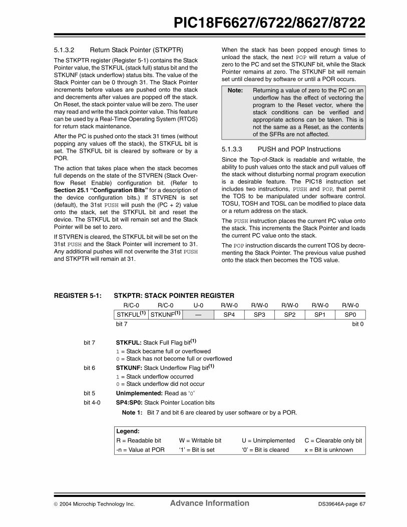
2004 Microchip Technology Inc. Advance Information DS39646A-page 67
PIC18F6627/6722/8627/8722
5.1.3.2 Return Stack Pointer (STKPTR)
The STKPTR register (Register 5-1) contains the StackPointer value, the STKFUL (stack full) status bit and theSTKUNF (stack underflow) status bits. The value of theStack Pointer can be 0 through 31. The Stack Pointerincrements before values are pushed onto the stackand decrements after values are popped off the stack.On Reset, the stack pointer value will be zero. The usermay read and write the stack pointer value. This featurecan be used by a Real-Time Operating System (RTOS)for return stack maintenance.
After the PC is pushed onto the stack 31 times (withoutpopping any values off the stack), the STKFUL bit isset. The STKFUL bit is cleared by software or by aPOR.
The action that takes place when the stack becomesfull depends on the state of the STVREN (Stack Over-flow Reset Enable) configuration bit. (Refer toSection 25.1 “Configuration Bits” for a description ofthe device configuration bits.) If STVREN is set(default), the 31st PUSH will push the (PC + 2) valueonto the stack, set the STKFUL bit and reset thedevice. The STKFUL bit will remain set and the StackPointer will be set to zero.
If STVREN is cleared, the STKFUL bit will be set on the31st PUSH and the Stack Pointer will increment to 31.Any additional pushes will not overwrite the 31st PUSHand STKPTR will remain at 31.
When the stack has been popped enough times tounload the stack, the next POP will return a value ofzero to the PC and set the STKUNF bit, while the StackPointer remains at zero. The STKUNF bit will remainset until cleared by software or until a POR occurs.
5.1.3.3 PUSH and POP Instructions
Since the Top-of-Stack is readable and writable, theability to push values onto the stack and pull values offthe stack without disturbing normal program executionis a desirable feature. The PIC18 instruction setincludes two instructions, PUSH and POP, that permitthe TOS to be manipulated under software control.TOSU, TOSH and TOSL can be modified to place dataor a return address on the stack.
The PUSH instruction places the current PC value ontothe stack. This increments the Stack Pointer and loadsthe current PC value onto the stack.
The POP instruction discards the current TOS by decre-menting the Stack Pointer. The previous value pushedonto the stack then becomes the TOS value.
REGISTER 5-1: STKPTR: STACK POINTER REGISTER
Note: Returning a value of zero to the PC on anunderflow has the effect of vectoring theprogram to the Reset vector, where thestack conditions can be verified andappropriate actions can be taken. This isnot the same as a Reset, as the contentsof the SFRs are not affected.
R/C-0 R/C-0 U-0 R/W-0 R/W-0 R/W-0 R/W-0 R/W-0
STKFUL(1) STKUNF(1) — SP4 SP3 SP2 SP1 SP0
bit 7 bit 0
bit 7 STKFUL: Stack Full Flag bit(1)
1 = Stack became full or overflowed 0 = Stack has not become full or overflowed
bit 6 STKUNF: Stack Underflow Flag bit(1)
1 = Stack underflow occurred 0 = Stack underflow did not occur
bit 5 Unimplemented: Read as ‘0’
bit 4-0 SP4:SP0: Stack Pointer Location bits
Note 1: Bit 7 and bit 6 are cleared by user software or by a POR.
Legend:
R = Readable bit W = Writable bit U = Unimplemented C = Clearable only bit
-n = Value at POR ‘1’ = Bit is set ‘0’ = Bit is cleared x = Bit is unknown
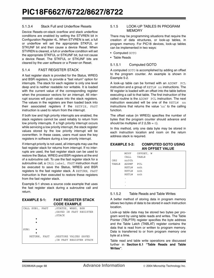
PIC18F6627/6722/8627/8722
DS39646A-page 68 Advance Information 2004 Microchip Technology Inc.
5.1.3.4 Stack Full and Underflow Resets
Device Resets-on-stack overflow and stack underflowconditions are enabled by setting the STVREN bit inConfiguration Register 4L. When STVREN is set, a fullor underflow will set the appropriate STKFUL orSTKUNF bit and then cause a device Reset. WhenSTVREN is cleared, a full or underflow condition will setthe appropriate STKFUL or STKUNF bit, but not causea device Reset. The STKFUL or STKUNF bits arecleared by the user software or a Power-on Reset.
5.1.4 FAST REGISTER STACK
A fast register stack is provided for the Status, WREGand BSR registers, to provide a “fast return” option forinterrupts. The stack for each register is only one leveldeep and is neither readable nor writable. It is loadedwith the current value of the corresponding registerwhen the processor vectors for an interrupt. All inter-rupt sources will push values into the stack registers.The values in the registers are then loaded back intotheir associated registers if the RETFIE, FASTinstruction is used to return from the interrupt.
If both low and high priority interrupts are enabled, thestack registers cannot be used reliably to return fromlow priority interrupts. If a high priority interrupt occurswhile servicing a low priority interrupt, the stack registervalues stored by the low priority interrupt will beoverwritten. In these cases, users must save the keyregisters in software during a low priority interrupt.
If interrupt priority is not used, all interrupts may use thefast register stack for returns from interrupt. If no inter-rupts are used, the fast register stack can be used torestore the Status, WREG and BSR registers at the endof a subroutine call. To use the fast register stack for asubroutine call, a CALL label, FAST instruction mustbe executed to save the Status, WREG and BSRregisters to the fast register stack. A RETURN, FASTinstruction is then executed to restore these registersfrom the fast register stack.
Example 5-1 shows a source code example that usesthe fast register stack during a subroutine call andreturn.
EXAMPLE 5-1: FAST REGISTER STACK CODE EXAMPLE
5.1.5 LOOK-UP TABLES IN PROGRAM MEMORY
There may be programming situations that require thecreation of data structures, or look-up tables, inprogram memory. For PIC18 devices, look-up tablescan be implemented in two ways:
• Computed GOTO
• Table Reads
5.1.5.1 Computed GOTO
A computed GOTO is accomplished by adding an offsetto the program counter. An example is shown inExample 5-2.
A look-up table can be formed with an ADDWF PCLinstruction and a group of RETLW nn instructions. TheW register is loaded with an offset into the table beforeexecuting a call to that table. The first instruction of thecalled routine is the ADDWF PCL instruction. The nextinstruction executed will be one of the RETLW nninstructions that returns the value ‘nn’ to the callingfunction.
The offset value (in WREG) specifies the number ofbytes that the program counter should advance andshould be multiples of 2 (LSb = 0).
In this method, only one data byte may be stored ineach instruction location and room on the returnaddress stack is required.
EXAMPLE 5-2: COMPUTED GOTO USING AN OFFSET VALUE
5.1.5.2 Table Reads and Table Writes
A better method of storing data in program memoryallows two bytes of data to be stored in each instructionlocation.
Look-up table data may be stored two bytes per pro-gram word by using table reads and writes. The TablePointer (TBLPTR) register specifies the byte addressand the Table Latch (TABLAT) register contains thedata that is read from or written to program memory.Data is transferred to or from program memory onebyte at a time.
Table read and table write operations are discussedfurther in Section 6.1 “Table Reads and TableWrites”.
CALL SUB1, FAST ;STATUS, WREG, BSR;SAVED IN FAST REGISTER;STACK
••
SUB1 ••
RETURN, FAST ;RESTORE VALUES SAVED;IN FAST REGISTER STACK
MOVF OFFSET, WCALL TABLE
ORG nn00hTABLE ADDWF PCL
RETLW nnhRETLW nnhRETLW nnh...

2004 Microchip Technology Inc. Advance Information DS39646A-page 69
PIC18F6627/6722/8627/8722
5.2 PIC18 Instruction Cycle
5.2.1 CLOCKING SCHEME
The microcontroller clock input, whether from an inter-nal or external source, is internally divided by four togenerate four non-overlapping quadrature clocks (Q1,Q2, Q3 and Q4). Internally, the program counter isincremented on every Q1; the instruction is fetchedfrom the program memory and latched into the instruc-tion register during Q4. The instruction is decoded andexecuted during the following Q1 through Q4. Theclocks and instruction execution flow are shown inFigure 5-4.
5.2.2 INSTRUCTION FLOW/PIPELINING
An “Instruction Cycle” consists of four Q cycles: Q1through Q4. The instruction fetch and execute arepipelined in such a manner that a fetch takes oneinstruction cycle, while the decode and execute takeanother instruction cycle. However, due to the pipe-lining, each instruction effectively executes in onecycle. If an instruction causes the program counter tochange (e.g., GOTO), then two cycles are required tocomplete the instruction (Example 5-3).
A fetch cycle begins with the program counterincrementing in Q1.
In the execution cycle, the fetched instruction is latchedinto the Instruction Register (IR) in cycle Q1. Thisinstruction is then decoded and executed during theQ2, Q3 and Q4 cycles. Data memory is read during Q2(operand read) and written during Q4 (destinationwrite).
FIGURE 5-4: CLOCK/INSTRUCTION CYCLE
EXAMPLE 5-3: INSTRUCTION PIPELINE FLOW
Q1 Q2 Q3 Q4 Q1 Q2 Q3 Q4 Q1 Q2 Q3 Q4
OSC1
Q1
Q2
Q3
Q4
PC
OSC2/CLKO(RC mode)
PC PC + 2 PC + 4
Fetch INST (PC)Execute INST (PC – 2)
Fetch INST (PC + 2)Execute INST (PC)
Fetch INST (PC + 4)Execute INST (PC + 2)
InternalPhaseClock
All instructions are single cycle, except for any program branches. These take two cycles since the fetch instructionis “flushed” from the pipeline while the new instruction is being fetched and then executed.
TCY0 TCY1 TCY2 TCY3 TCY4 TCY5
1. MOVLW 55h Fetch 1 Execute 1
2. MOVWF PORTB Fetch 2 Execute 2
3. BRA SUB_1 Fetch 3 Execute 3
4. BSF PORTA, BIT3 (Forced NOP) Fetch 4 Flush (NOP)
5. Instruction @ address SUB_1 Fetch SUB_1 Execute SUB_1
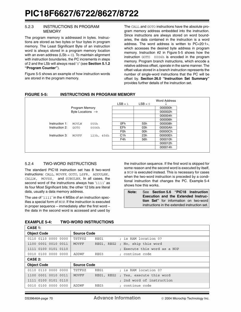
PIC18F6627/6722/8627/8722
DS39646A-page 70 Advance Information 2004 Microchip Technology Inc.
5.2.3 INSTRUCTIONS IN PROGRAM MEMORY
The program memory is addressed in bytes. Instruc-tions are stored as two bytes or four bytes in programmemory. The Least Significant Byte of an instructionword is always stored in a program memory locationwith an even address (LSb = 0). To maintain alignmentwith instruction boundaries, the PC increments in stepsof 2 and the LSb will always read ‘0’ (see Section 5.1.2“Program Counter”).
Figure 5-5 shows an example of how instruction wordsare stored in the program memory.
The CALL and GOTO instructions have the absolute pro-gram memory address embedded into the instruction.Since instructions are always stored on word bound-aries, the data contained in the instruction is a wordaddress. The word address is written to PC<20:1>,which accesses the desired byte address in programmemory. Instruction #2 in Figure 5-5 shows how theinstruction GOTO 0006h is encoded in the programmemory. Program branch instructions, which encode arelative address offset, operate in the same manner. Theoffset value stored in a branch instruction represents thenumber of single-word instructions that the PC will beoffset by. Section 26.0 “Instruction Set Summary”provides further details of the instruction set.
FIGURE 5-5: INSTRUCTIONS IN PROGRAM MEMORY
5.2.4 TWO-WORD INSTRUCTIONS
The standard PIC18 instruction set has 8 two-wordinstructions: CALL, MOVFF, GOTO, LSFR, ADDULNK,CALLW, MOVSS, and SUBULNK. In all cases, thesecond word of the instructions always has ‘1111’ asits four Most Significant bits; the other 12 bits are literaldata, usually a data memory address.
The use of ‘1111’ in the 4 MSbs of an instruction spec-ifies a special form of NOP. If the instruction is executedin proper sequence – immediately after the first word –the data in the second word is accessed and used by
the instruction sequence. If the first word is skipped forsome reason and the second word is executed by itself,a NOP is executed instead. This is necessary for caseswhen the two-word instruction is preceded by a condi-tional instruction that changes the PC. Example 5-4shows how this works.
EXAMPLE 5-4: TWO-WORD INSTRUCTIONS
Word AddressLSB = 1 LSB = 0 ↓
Program MemoryByte Locations →
000000h000002h000004h000006h
Instruction 1: MOVLW 055h 0Fh 55h 000008hInstruction 2: GOTO 0006h EFh 03h 00000Ah
F0h 00h 00000ChInstruction 3: MOVFF 123h, 456h C1h 23h 00000Eh
F4h 56h 000010h000012h000014h
Note: See Section 5.6 “PIC18 InstructionExecution and the Extended Instruc-tion Set” for information on two-wordinstructions in the extended instruction set.
CASE 1:
Object Code Source Code0110 0110 0000 0000 TSTFSZ REG1 ; is RAM location 0?
1100 0001 0010 0011 MOVFF REG1, REG2 ; No, skip this word
1111 0100 0101 0110 ; Execute this word as a NOP
0010 0100 0000 0000 ADDWF REG3 ; continue code
CASE 2:
Object Code Source Code0110 0110 0000 0000 TSTFSZ REG1 ; is RAM location 0?
1100 0001 0010 0011 MOVFF REG1, REG2 ; Yes, execute this word
1111 0100 0101 0110 ; 2nd word of instruction
0010 0100 0000 0000 ADDWF REG3 ; continue code

2004 Microchip Technology Inc. Advance Information DS39646A-page 71
PIC18F6627/6722/8627/8722
5.3 Data Memory Organization
The data memory in PIC18 devices is implemented asstatic RAM. Each register in the data memory has a12-bit address, allowing up to 4096 bytes of datamemory. The memory space is divided into as many as16 banks that contain 256 bytes each; PIC18F6627/6722/8627/8722 devices implement all 16 banks.Figure 5-6 shows the data memory organization for thePIC18F6627/6722/8627/8722 devices.
The data memory contains Special Function Registers(SFRs) and General Purpose Registers (GPRs). TheSFRs are used for control and status of the controllerand peripheral functions, while GPRs are used for datastorage and scratchpad operations in the user’sapplication. Any read of an unimplemented location willread as ‘0’s.
The instruction set and architecture allow operationsacross all banks. The entire data memory may beaccessed by Direct, Indirect or Indexed Addressingmodes. Addressing modes are discussed later in thissubsection.
To ensure that commonly used registers (SFRs andselect GPRs) can be accessed in a single cycle, PIC18devices implement an Access Bank. This is a 256-bytememory space that provides fast access to SFRs andthe lower portion of GPR Bank 0 without using theBSR. Section 5.3.2 “Access Bank” provides adetailed description of the Access RAM.
5.3.1 BANK SELECT REGISTER (BSR)
Large areas of data memory require an efficientaddressing scheme to make rapid access to anyaddress possible. Ideally, this means that an entireaddress does not need to be provided for each read orwrite operation. For PIC18 devices, this is accom-plished with a RAM banking scheme. This divides thememory space into 16 contiguous banks of 256 bytes.Depending on the instruction, each location can beaddressed directly by its full 12-bit address, or an 8-bitlow-order address and a 4-bit bank pointer.
Most instructions in the PIC18 instruction set make useof the bank pointer, known as the Bank Select Register(BSR). This SFR holds the 4 Most Significant bits of alocation’s address; the instruction itself includes the8 Least Significant bits. Only the four lower bits of theBSR are implemented (BSR3:BSR0). The upper fourbits are unused; they will always read ‘0’ and cannot bewritten to. The BSR can be loaded directly by using theMOVLB instruction.
The value of the BSR indicates the bank in datamemory; the 8 bits in the instruction show the locationin the bank and can be thought of as an offset from thebank’s lower boundary. The relationship between theBSR’s value and the bank division in data memory isshown in Figure 5-7.
Since up to 16 registers may share the same low-orderaddress, the user must always be careful to ensure thatthe proper bank is selected before performing a dataread or write. For example, writing what should beprogram data to an 8-bit address of F9h while the BSRis 0Fh will end up resetting the program counter.
While any bank can be selected, only those banks thatare actually implemented can be read or written to.Writes to unimplemented banks are ignored, whilereads from unimplemented banks will return ‘0’s. Evenso, the Status register will still be affected as if theoperation was successful. The data memory map inFigure 5-6 indicates which banks are implemented.
In the core PIC18 instruction set, only the MOVFFinstruction fully specifies the 12-bit address of thesource and target registers. This instruction ignores theBSR completely when it executes. All other instructionsinclude only the low-order address as an operand andmust use either the BSR or the Access Bank to locatetheir target registers.
Note: The operation of some aspects of datamemory are changed when the PIC18extended instruction set is enabled. SeeSection 5.5 “Data Memory and theExtended Instruction Set” for moreinformation.

PIC18F6627/6722/8627/8722
DS39646A-page 72 Advance Information 2004 Microchip Technology Inc.
FIGURE 5-6: DATA MEMORY MAP FOR PIC18F6627/6722/8627/8722 DEVICES
Bank 0
Bank 1
Bank 14
Bank 15
Data Memory MapBSR<3:0>
= 0000
= 0001
= 1111
060h05Fh
F60hFFFh
00h
5Fh60h
FFh
Access Bank
When ‘a’ = 0:
The BSR is ignored and theAccess Bank is used.
The first 128 bytes are general purpose RAM (from Bank 0).
The second 128 bytes areSpecial Function Registers(from Bank 15).
When ‘a’ = 1:
The BSR specifies the Bankused by the instruction.
F5FhF00hEFFh
1FFh
100h0FFh
000hAccess RAM
FFh
00h
FFh
00h
FFh
00h
GPR
GPR
SFR
Access RAM High
Access RAM Low
Bank 2
= 0110
= 0010
(SFRs)
2FFh
200h
3FFh
300h
4FFh
400h
5FFh
500h
6FFh
600h
7FFh
700h
8FFh
800h
9FFh
900h
AFFh
A00h
BFFh
B00h
CFFh
C00h
DFFh
D00h
E00h
Bank 3
Bank 4
Bank 5
Bank 6
Bank 7
Bank 8
Bank 9
Bank 10
Bank 11
Bank 12
Bank 13
FFh
00h
FFh
00h
FFh
00h
FFh
00h
FFh
00h
FFh
00h
FFh
00h
FFh
00h
FFh
00h
FFh
00h
FFh
00h
FFh
00h
GPR
FFh
00h
= 0011
= 0100
= 0101
= 0111
= 1000
= 1001
= 1010
= 1011
= 1100
= 1101
= 1110
Unused
GPR
GPR
GPR
GPR
GPR
GPR
GPR
GPR
GPR
GPR
GPR
GPR

2004 Microchip Technology Inc. Advance Information DS39646A-page 73
PIC18F6627/6722/8627/8722FIGURE 5-7: USE OF THE BANK SELECT REGISTER (DIRECT ADDRESSING)
5.3.2 ACCESS BANK
While the use of the BSR with an embedded 8-bitaddress allows users to address the entire range ofdata memory, it also means that the user must alwaysensure that the correct bank is selected. Otherwise,data may be read from or written to the wrong location.This can be disastrous if a GPR is the intended targetof an operation, but an SFR is written to instead.Verifying and/or changing the BSR for each read orwrite to data memory can become very inefficient.
To streamline access for the most commonly used datamemory locations, the data memory is configured withan Access Bank, which allows users to access amapped block of memory without specifying a BSR.The Access Bank consists of the first 96 bytes of mem-ory (00h-5Fh) in Bank 0 and the last 160 bytes of mem-ory (60h-FFh) in Block 15. The lower half is known asthe “Access RAM” and is composed of GPRs. Thisupper half is also where the device’s SFRs aremapped. These two areas are mapped contiguously inthe Access Bank and can be addressed in a linearfashion by an 8-bit address (Figure 5-6).
The Access Bank is used by core PIC18 instructionsthat include the Access RAM bit (the ‘a’ parameter inthe instruction). When ‘a’ is equal to ‘1’, the instructionuses the BSR and the 8-bit address included in theopcode for the data memory address. When ‘a’ is ‘0’,
however, the instruction is forced to use the AccessBank address map; the current value of the BSR isignored entirely.
Using this “forced” addressing allows the instruction tooperate on a data address in a single cycle, withoutupdating the BSR first. For 8-bit addresses of 60h andabove, this means that users can evaluate and operateon SFRs more efficiently. The Access RAM below 60his a good place for data values that the user might needto access rapidly, such as immediate computationalresults or common program variables. Access RAMalso allows for faster and more code efficient contextsaving and switching of variables.
The mapping of the Access Bank is slightly differentwhen the extended instruction set is enabled (XINSTconfiguration bit = 1). This is discussed in more detailin Section 5.5.3 “Mapping the Access Bank inIndexed Literal Offset Mode”.
5.3.3 GENERAL PURPOSE REGISTER FILE
PIC18 devices may have banked memory in the GPRarea. This is data RAM, which is available for use by allinstructions. GPRs start at the bottom of Bank 0(address 000h) and grow upwards towards the bottom ofthe SFR area. GPRs are not initialized by a Power-onReset and are unchanged on all other Resets.
Note 1: The Access RAM bit of the instruction can be used to force an override of the selected bank (BSR<3:0>) to the registers of the Access Bank.
2: The MOVFF instruction embeds the entire 12-bit address in the instruction.
Data Memory
Bank Select(2)
7 0From Opcode(2)
0 0 0 0
000h
100h
200h
300h
F00h
E00h
FFFh
Bank 0
Bank 1
Bank 2
Bank 14
Bank 15
00h
FFh00h
FFh00h
FFh
00h
FFh00h
FFh
00h
FFh
Bank 3throughBank 13
0 0 1 1 1 1 1 1 1 1 1 1
7 0BSR(1)
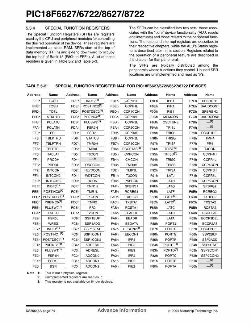
PIC18F6627/6722/8627/8722
DS39646A-page 74 Advance Information 2004 Microchip Technology Inc.
5.3.4 SPECIAL FUNCTION REGISTERS
The Special Function Registers (SFRs) are registersused by the CPU and peripheral modules for controllingthe desired operation of the device. These registers areimplemented as static RAM. SFRs start at the top ofdata memory (FFFh) and extend downward to occupythe top half of Bank 15 (F80h to FFFh). A list of theseregisters is given in Table 5-2 and Table 5-3.
The SFRs can be classified into two sets: those asso-ciated with the “core” device functionality (ALU, resetsand interrupts) and those related to the peripheral func-tions. The reset and interrupt registers are described intheir respective chapters, while the ALU’s Status regis-ter is described later in this section. Registers related tothe operation of a peripheral feature are described inthe chapter for that peripheral.
The SFRs are typically distributed among theperipherals whose functions they control. Unused SFRlocations are unimplemented and read as ‘0’s.
TABLE 5-2: SPECIAL FUNCTION REGISTER MAP FOR PIC18F6627/6722/8627/8722 DEVICES
Address Name Address Name Address Name Address Name Address Name
FFFh TOSU FDFh INDF2(1) FBFh CCPR1H F9Fh IPR1 F7Fh SPBRGH1
FFEh TOSH FDEh POSTINC2(1) FBEh CCPR1L F9Eh PIR1 F7Eh BAUDCON1
FFDh TOSL FDDh POSTDEC2(1) FBDh CCP1CON F9Dh PIE1 F7Dh SPBRGH2
FFCh STKPTR FDCh PREINC2(1) FBCh CCPR2H F9Ch MEMCON F7Ch BAUDCON2
FFBh PCLATU FDBh PLUSW2(1) FBBh CCPR2L F9Bh OSCTUNE F7Bh —(2)
FFAh PCLATH FDAh FSR2H FBAh CCP2CON F9Ah TRISJ F7Ah —(2)
FF9h PCL FD9h FSR2L FB9h CCPR3H F99h TRISH F79h ECCP1DEL
FF8h TBLPTRU FD8h STATUS FB8h CCPR3L F98h TRISG F78h TMR4
FF7h TBLPTRH FD7h TMR0H FB7h CCP3CON F97h TRISF F77h PR4
FF6h TBLPTRL FD6h TMR0L FB6h ECCP1AS(3) F96h TRISE(3) F76h T4CON
FF5h TABLAT FD5h T0CON FB5h CVRCON F95h TRISD(3) F75h CCPR4H
FF4h PRODH FD4h —(2) FB4h CMCON F94h TRISC F74h CCPR4L
FF3h PRODL FD3h OSCCON FB3h TMR3H F93h TRISB F73h CCP4CON
FF2h INTCON FD2h HLVDCON FB2h TMR3L F92h TRISA F72h CCPR5H
FF1h INTCON2 FD1h WDTCON FB1h T3CON F91h LATJ F71h CCPR5L
FF0h INTCON3 FD0h RCON FB0h PSPCON F90h LATH F70h CCP5CON
FEFh INDF0(1) FCFh TMR1H FAFh SPBRG1 F8Fh LATG F6Fh SPBRG2
FEEh POSTINC0(1) FCEh TMR1L FAEh RCREG1 F8Eh LATF F6Eh RCREG2
FEDh POSTDEC0(1) FCDh T1CON FADh TXREG1 F8Dh LATE(3) F6Dh TXREG2
FECh PREINC0(1) FCCh TMR2 FACh TXSTA1 F8Ch LATD(3) F6Ch TXSTA2
FEBh PLUSW0(1) FCBh PR2 FABh RCSTA1 F8Bh LATC F6Bh RCSTA2
FEAh FSR0H FCAh T2CON FAAh EEADRH F8Ah LATB F6Ah ECCP3AS
FE9h FSR0L FC9h SSP1BUF FA9h EEADR F89h LATA F69h ECCP3DEL
FE8h WREG FC8h SSP1ADD FA8h EEDATA F88h PORTJ F68h ECCP2AS
FE7h INDF1(1) FC7h SSP1STAT FA7h EECON2(1) F87h PORTH F67h ECCP2DEL
FE6h POSTINC1(1) FC6h SSP1CON1 FA6h EECON1 F86h PORTG F66h SSP2BUF
FE5h POSTDEC1(1) FC5h SSP1CON2 FA5h IPR3 F85h PORTF F65h SSP2ADD
FE4h PREINC1(1) FC4h ADRESH FA4h PIR3 F84h PORTE(3) F64h SSP2STAT
FE3h PLUSW1(1) FC3h ADRESL FA3h PIE3 F83h PORTD(3) F63h SSP2CON1
FE2h FSR1H FC2h ADCON0 FA2h IPR2 F82h PORTC F62h SSP2CON2
FE1h FSR1L FC1h ADCON1 FA1h PIR2 F81h PORTB F61h —(2)
FE0h BSR FC0h ADCON2 FA0h PIE2 F80h PORTA F60h —(2)
Note 1: This is not a physical register.2: Unimplemented registers are read as ‘0’.3: This register is not available on 64-pin devices.

2004 Microchip Technology Inc. Advance Information DS39646A-page 75
PIC18F6627/6722/8627/8722
TABLE 5-3: REGISTER FILE SUMMARY
Filename Bit 7 Bit 6 Bit 5 Bit 4 Bit 3 Bit 2 Bit 1 Bit 0 Value on POR, BOR
Details on page:
TOSU — — — Top-of-Stack Upper Byte (TOS<20:16>) ---0 0000 57, 66
TOSH Top-of-Stack High Byte (TOS<15:8>) 0000 0000 57, 66
TOSL Top-of-Stack Low Byte (TOS<7:0>) 0000 0000 57, 66
STKPTR STKFUL(6) STKUNF(6) — Return Stack Pointer 00-0 0000 57, 67
PCLATU — — bit 21(1) Holding Register for PC<20:16> ---0 0000 57, 66
PCLATH Holding Register for PC<15:8> 0000 0000 57, 66
PCL PC Low Byte (PC<7:0>) 0000 0000 57, 66
TBLPTRU — — — Program Memory Table Pointer Upper Byte (TBLPTR<20:16>) --00 0000 57, 88
TBLPTRH Program Memory Table Pointer High Byte (TBLPTR<15:8>) 0000 0000 57, 88
TBLPTRL Program Memory Table Pointer Low Byte (TBLPTR<7:0>) 0000 0000 57, 88
TABLAT Program Memory Table Latch 0000 0000 57, 88
PRODH Product Register High Byte xxxx xxxx 57, 115
PRODL Product Register Low Byte xxxx xxxx 57, 115
INTCON GIE/GIEH PEIE/GIEL TMR0IE INT0IE RBIE TMR0IF INT0IF RBIF 0000 000x 57, 119
INTCON2 RBPU INTEDG0 INTEDG1 INTEDG2 INTEDG3 TMR0IP INT3IP RBIP 1111 1111 57, 120
INTCON3 INT2IP INT1IP INT3IE INT2IE INT1IE INT3IF INT2IF INT1IF 1100 0000 57, 121
INDF0 Uses contents of FSR0 to address data memory - value of FSR0 not changed (not a physical register) N/A 57, 81
POSTINC0 Uses contents of FSR0 to address data memory - value of FSR0 post-incremented (not a physical register) N/A 57, 81
POSTDEC0 Uses contents of FSR0 to address data memory - value of FSR0 post-decremented (not a physical register) N/A 57, 81
PREINC0 Uses contents of FSR0 to address data memory - value of FSR0 pre-incremented (not a physical register) N/A 57, 81
PLUSW0 Uses contents of FSR0 to address data memory - value of FSR0 pre-incremented (not a physical register) - value of FSR0 offset by W
N/A 57, 81
FSR0H — — — — Indirect Data Memory Address Pointer 0 High ---- 0000 57, 81
FSR0L Indirect Data Memory Address Pointer 0 Low Byte xxxx xxxx 57, 81
WREG Working Register xxxx xxxx 57
INDF1 Uses contents of FSR1 to address data memory - value of FSR1 not changed (not a physical register) N/A 57, 81
POSTINC1 Uses contents of FSR1 to address data memory - value of FSR1 post-incremented (not a physical register) N/A 57, 81
POSTDEC1 Uses contents of FSR1 to address data memory - value of FSR1 post-decremented (not a physical register) N/A 57, 81
PREINC1 Uses contents of FSR1 to address data memory - value of FSR1 pre-incremented (not a physical register) N/A 57, 81
PLUSW1 Uses contents of FSR1 to address data memory - value of FSR1 pre-incremented (not a physical register) - value of FSR1 offset by W
N/A 57, 81
FSR1H — — — — Indirect Data Memory Address Pointer 1 High ---- 0000 58, 81
FSR1L Indirect Data Memory Address Pointer 1 Low Byte xxxx xxxx 58, 81
BSR — — — — Bank Select Register ---- 0000 58, 71
INDF2 Uses contents of FSR2 to address data memory - value of FSR2 not changed (not a physical register) N/A 58, 81
POSTINC2 Uses contents of FSR2 to address data memory - value of FSR2 post-incremented (not a physical register) N/A 58, 81
POSTDEC2 Uses contents of FSR2 to address data memory - value of FSR2 post-decremented (not a physical register) N/A 58, 81
PREINC2 Uses contents of FSR2 to address data memory - value of FSR2 pre-incremented (not a physical register) N/A 58, 81
PLUSW2 Uses contents of FSR2 to address data memory - value of FSR2 pre-incremented (not a physical register) - value of FSR2 offset by W
N/A 58, 81
FSR2H — — — — Indirect Data Memory Address Pointer 2 High ---- 0000 58, 81
FSR2L Indirect Data Memory Address Pointer 2 Low Byte xxxx xxxx 58, 81Legend x = unknown, u = unchanged, - = unimplemented, q = value depends on conditionNote 1: The SBOREN bit is only available when the BOREN1:BOREN0 configuration bits = 01; otherwise, this bit reads as ‘0’.
2: These registers and/or bits are not implemented on 64-pin devices and are read as ‘0’. Reset values are shown for 80-pin devices; individual unimplemented bits should be interpreted as ‘-’.
3: The PLLEN bit is only available in specific oscillator configuration; otherwise it is disabled and reads as ‘0’. See Section 2.6.4 “PLL in INTOSC Modes”.
4: RA6/RA7 and their associated latch and direction bits are individually configured as port pins based on various primary oscillator modes. When disabled, these bits read as ‘0’.
5: RG5 is only available when Master Clear is disabled (MCLRE configuration bit = 0). Otherwise, RG5 reads as ‘0’.6: Bit 7 and Bit 6 are cleared by user software or by a POR.

PIC18F6627/6722/8627/8722
DS39646A-page 76 Advance Information 2004 Microchip Technology Inc.
STATUS — — — N OV Z DC C ---x xxxx 58, 79
TMR0H Timer0 register high byte 0000 0000 58, 163
TMR0L Timer0 register low byte xxxx xxxx 58, 163
T0CON TMR0ON T08BIT T0CS T0SE PSA T0PS2 T0PS1 T0PS0 1111 1111 58, 161
OSCCON IDLEN IRCF2 IRCF1 IRCF0 OSTS IOFS SCS1 SCS0 0100 q000 39, 58
HLVDCON VDIRMAG — IRVST HLVDEN HLVDL3 HLVDL2 HLVDL1 HLVDL0 0-00 0101 58, 289
WDTCON — — — — — — — SWDTEN --- ---0 58, 309
RCON IPEN SBOREN(1) — RI TO PD POR BOR 0q-1 11q0 50, 56, 58, 131
TMR1H Timer1 Register High Byte xxxx xxxx 58, 169
TMR1L Timer1 Register Low Bytes xxxx xxxx 58, 169
T1CON RD16 T1RUN T1CKPS1 T1CKPS0 T1OSCEN T1SYNC TMR1CS TMR1ON 0000 0000 58, 165
TMR2 Timer2 Register 0000 0000 58, 172
PR2 Timer2 Period Register 1111 1111 58, 172
T2CON — T2OUTPS3 T2OUTPS2 T2OUTPS1 T2OUTPS0 TMR2ON T2CKPS1 T2CKPS0 -000 0000 58, 171
SSP1BUF MSSP1 Receive Buffer/Transmit Register xxxx xxxx 58, 169, 170
SSP1ADD MSSP1 Address Register in I2C Slave Mode. MSSP1 Baud Rate Reload Register in I2C Master Mode. 0000 0000 58, 170
SSP1STAT SMP CKE D/A P S R/W UA BF 0000 0000 58, 162, 171
SSP1CON1 WCOL SSPOV SSPEN CKP SSPM3 SSPM2 SSPM1 SSPM0 0000 0000 58, 163, 172
SSP1CON2 GCEN ACKSTAT ACKDT ACKEN RCEN PEN RSEN SEN 0000 0000 58, 173
ADRESH A/D Result Register High Byte xxxx xxxx 59, 278
ADRESL A/D Result Register Low Byte xxxx xxxx 59, 278
ADCON0 — — CHS3 CHS2 CHS1 CHS0 GO/DONE ADON --00 0000 59, 269
ADCON1 — — VCFG1 VCFG0 PCFG3 PCFG2 PCFG1 PCFG0 --00 0000 59, 270
ADCON2 ADFM — ACQT2 ACQT1 ACQT0 ADCS2 ADCS1 ADCS0 0-00 0000 59, 271
CCPR1H Capture/Compare/PWM Register 1 High Byte xxxx xxxx 59, 180
CCPR1L Capture/Compare/PWM Register 1 Low Byte xxxx xxxx 59, 180
CCP1CON P1M1 P1M0 DC1B1 DC1B0 CCP1M3 CCP1M2 CCP1M1 CCP1M0 0000 0000 59, 187
CCPR2H Capture/Compare/PWM Register 2 High Byte xxxx xxxx 59, 180
CCPR2L Capture/Compare/PWM Register 2 Low Byte xxxx xxxx 59, 180
CCP2CON P2M1 P2M0 DC2B1 DC2B0 CCP2M3 CCP2M2 CCP2M1 CCP2M0 0000 0000 59, 179
CCPR3H Capture/Compare/PWM Register 3 High Byte xxxx xxxx 59, 180
CCPR3L Capture/Compare/PWM Register 3 Low Byte xxxx xxxx 59, 180
CCP3CON P3M1 P3M0 DC3B1 DC3B0 CCP3M3 CCP3M2 CCP3M1 CCP3M0 0000 0000 59, 179
ECCP1AS ECCP1ASE ECCP1AS2 ECCP1AS1 ECCP1AS0 PSS1AC1 PSS1AC0 PSS1BD1 PSS1BD0 0000 0000 59, 201
CVRCON CVREN CVROE CVRR CVRSS CVR3 CVR2 CVR1 CVR0 0000 0000 59, 285
CMCON C2OUT C1OUT C2INV C1INV CIS CM2 CM1 CM0 0000 0000 59, 279
TMR3H Timer3 Register High Byte xxxx xxxx 59, 175
TMR3L Timer3 Register Low Byte xxxx xxxx 59, 175
T3CON RD16 T3CCP2 T3CKPS1 T3CKPS0 T3CCP1 T3SYNC TMR3CS TMR3ON 0000 0000 59, 173
TABLE 5-3: REGISTER FILE SUMMARY (CONTINUED)
Filename Bit 7 Bit 6 Bit 5 Bit 4 Bit 3 Bit 2 Bit 1 Bit 0 Value on POR, BOR
Details on page:
Legend x = unknown, u = unchanged, - = unimplemented, q = value depends on conditionNote 1: The SBOREN bit is only available when the BOREN1:BOREN0 configuration bits = 01; otherwise, this bit reads as ‘0’.
2: These registers and/or bits are not implemented on 64-pin devices and are read as ‘0’. Reset values are shown for 80-pin devices; individual unimplemented bits should be interpreted as ‘-’.
3: The PLLEN bit is only available in specific oscillator configuration; otherwise it is disabled and reads as ‘0’. See Section 2.6.4 “PLL in INTOSC Modes”.
4: RA6/RA7 and their associated latch and direction bits are individually configured as port pins based on various primary oscillator modes. When disabled, these bits read as ‘0’.
5: RG5 is only available when Master Clear is disabled (MCLRE configuration bit = 0). Otherwise, RG5 reads as ‘0’.6: Bit 7 and Bit 6 are cleared by user software or by a POR.

2004 Microchip Technology Inc. Advance Information DS39646A-page 77
PIC18F6627/6722/8627/8722
PSPCON IBF OBF IBOV PSPMODE — — — — 0000 ---- 59, 252
SPBRG1 EUSART1 Baud Rate Generator, Low Byte 0000 0000 59, 252
RCREG1 EUSART1 Receive Register 0000 0000 59, 260
TXREG1 EUSART1 Transmit Register 0000 0000 59, 257
TXSTA1 CSRC TX9 TXEN SYNC SENDB BRGH TRMT TX9D 0000 0010 59, 248
RCSTA1 SPEN RX9 SREN CREN ADDEN FERR OERR RX9D 0000 000x 59, 249
EEADRH — — — — — — EE addr register high ---- --00 59, 109
EEADR EEPROM address register 0000 0000 59, 109
EEDATA EEPROM data register 0000 0000 59, 109
EECON2 EEPROM control register 2 (not a physical register) 0000 0000 59, 86
EECON1 EEPGD CFGS — FREE WRERR WREN WR RD xx-0 x000 59, 87
IPR3 SSP2IP BCL2IP RC2IP TX2IP TMR4IP CCP5IP CCP4IP CCP3IP 1111 1111 60, 129
PIR3 SSP2IF BCL2IF RC2IF TX2IF TMR4IF CCP5IF CCP4IF CCP3IF 0000 0000 60, 123
PIE3 SSP2IE BCL2IE RC2IE TX2IE TMR4IE CCP5IE CCP4IE CCP3IE 0000 0000 60, 126
IPR2 OSCFIP CMIP — EEIP BCL1IP HLVDIP TMR3IP CCP2IP 11-1 1111 60, 129
PIR2 OSCFIF CMIF — EEIF BCL1IF HLVDIF TMR3IF CCP2IF 00-0 0000 60, 123
PIE2 OSCFIE CMIE — EEIE BCL1IE HLVDIE TMR3IE CCP2IE 00-0 0000 60, 126
IPR1 PSPIP ADIP RC1IP TX1IP SSP1IP CCP1IP TMR2IP TMR1IP 1111 1111 60, 128
PIR1 PSPIF ADIF RC1IF TX1IF SSP1IF CCP1IF TMR2IF TMR1IF 0000 0000 60, 122
PIE1 PSPIE ADIE RC1IE TX1IE SSP1IE CCP1IE TMR2IE TMR1IE 0000 0000 60, 125
MEMCON(2) EBDIS — WAIT1 WAIT0 — — WM1 WM0 0-00 --00 60, 96
OSCTUNE INTSRC PLLEN(3) — TUN4 TUN3 TUN2 TUN1 TUN0 00-0 0000 35, 60
TRISJ(2) Data Direction Control Register for PORTJ 1111 1111 60, 157
TRISH(2) Data Direction Control Register for PORTH 1111 1111 60, 155
TRISG — — — Data Direction Control Register for PORTG ---1 1111 60, 152
TRISF Data Direction Control Register for PORTF 1111 1111 60, 149
TRISE Data Direction Control Register for PORTE 1111 1111 60, 147
TRISD Data Direction Control Register for PORTD 1111 1111 60, 142
TRISC Data Direction Control Register for PORTC 1111 1111 60, 139
TRISB Data Direction Control Register for PORTB 1111 1111 60, 136
TRISA TRISA7(4) TRISA6(4) Data Direction Control Register for PORTA 1111 1111 60, 133
LATJ(2) Read PORTJ Data Latch, Write PORTJ Data Latch xxxx xxxx 60, 156
LATH(2) Read PORTH Data Latch, Write PORTH Data Latch xxxx xxxx 60, 153
LATG — — — Read PORTG Data Latch, Write PORTG Data Latch ---x xxxx 60, 150
LATF Read PORTF Data Latch, Write PORTF Data Latch xxxx xxxx 60, 148
LATE Read PORTE Data Latch, Write PORTE Data Latch xxxx xxxx 60, 145
LATD Read PORTD Data Latch, Write PORTD Data Latch xxxx xxxx 60, 142
LATC Read PORTC Data Latch, Write PORTC Data Latch xxxx xxxx 60, 139
LATB Read PORTB Data Latch, Write PORTB Data Latch xxxx xxxx 60, 136
LATA LATA7(4) LATA6(4) Read PORTA Data Latch, Write PORTA Data Latch xxxx xxxx 60, 133
TABLE 5-3: REGISTER FILE SUMMARY (CONTINUED)
Filename Bit 7 Bit 6 Bit 5 Bit 4 Bit 3 Bit 2 Bit 1 Bit 0 Value on POR, BOR
Details on page:
Legend x = unknown, u = unchanged, - = unimplemented, q = value depends on conditionNote 1: The SBOREN bit is only available when the BOREN1:BOREN0 configuration bits = 01; otherwise, this bit reads as ‘0’.
2: These registers and/or bits are not implemented on 64-pin devices and are read as ‘0’. Reset values are shown for 80-pin devices; individual unimplemented bits should be interpreted as ‘-’.
3: The PLLEN bit is only available in specific oscillator configuration; otherwise it is disabled and reads as ‘0’. See Section 2.6.4 “PLL in INTOSC Modes”.
4: RA6/RA7 and their associated latch and direction bits are individually configured as port pins based on various primary oscillator modes. When disabled, these bits read as ‘0’.
5: RG5 is only available when Master Clear is disabled (MCLRE configuration bit = 0). Otherwise, RG5 reads as ‘0’.6: Bit 7 and Bit 6 are cleared by user software or by a POR.

PIC18F6627/6722/8627/8722
DS39646A-page 78 Advance Information 2004 Microchip Technology Inc.
PORTJ(2) Read PORTJ pins, Write PORTJ Data Latch xxxx xxxx 60, 156
PORTH(2) Read PORTH pins, Write PORTH Data Latch 0000 xxxx 60, 153
PORTG — — RG5(5) Read PORTG pins, Write PORTG Data Latch --xx xxxx 60, 150
PORTF Read PORTF pins, Write PORTF Data Latch x000 0000 60, 148
PORTE Read PORTE pins, Write PORTE Data Latch xxxx xxxx 60, 145
PORTD Read PORTD pins, Write PORTD Data Latch xxxx xxxx 60, 142
PORTC Read PORTC pins, Write PORTC Data Latch xxxx xxxx 60, 139
PORTB Read PORTB pins, Write PORTB Data Latch xxxx xxxx 60, 136
PORTA RA7(4) RA6(4) Read PORTA pins, Write PORTA Data Latch xx0x 0000 61, 133
SPBRGH1 EUSART1 Baud Rate Generator High byte 0000 0000 61, 252
BAUDCON1 ABDOVF RCIDL — SCKP BRG16 — WUE ABDEN 01-0 0-00 61, 250
SPBRGH2 EUSART2 Baud Rate Generator High byte 0000 0000 61, 252
BAUDCON2 ABDOVF RCIDL — SCKP BRG16 — WUE ABDEN 01-0 0-00 61, 250
ECCP1DEL P1RSEN P1DC6 P1DC5 P1DC4 P1DC3 P1DC2 P1DC1 P1DC0 0000 0000 61, 200
TMR4 Timer4 Register 0000 0000 61, 178
PR4 Timer4 Period Register 1111 1111 61, 178
T4CON — T4OUTPS3 T4OUTPS2 T4OUTPS1 T4OUTPS0 TMR4ON T4CKPS1 T4CKPS0 -000 0000 61, 178
CCPR4H Capture/Compare/PWM Register 4 High Byte xxxx xxxx 61, 180
CCPR4L Capture/Compare/PWM Register 4 Low Byte xxxx xxxx 61, 180
CCP4CON — — DC4B1 DC4B0 CCP4M3 CCP4M2 CCP4M1 CCP4M0 --00 0000 61, 179
CCPR5H Capture/Compare/PWM Register 5 High Byte xxxx xxxx 61, 180
CCPR5L Capture/Compare/PWM Register 5 Low Byte xxxx xxxx 61, 180
CCP5CON — — DC5B1 DC5B0 CCP5M3 CCP5M2 CCP5M1 CCP5M0 --00 0000 61, 179
SPBRG2 EUSART2 Baud Rate Generator, Low Byte 0000 0000 61, 252
RCREG2 EUSART2 Receive Register 0000 0000 61, 260
TXREG2 EUSART2 Transmit Register 0000 0000 61, 257
TXSTA2 CSRC TX9 TXEN SYNC SENDB BRGH TRMT TX9D 0000 0010 61, 248
RCSTA2 SPEN RX9 SREN CREN ADDEN FERR OERR RX9D 0000 000x 61, 249
ECCP3AS ECCP3ASE ECCP3AS2 ECCP3AS1 ECCP3AS0 PSS3AC1 PSS3AC0 PSS3BD1 PSS3BD0 0000 0000 61, 201
ECCP3DEL P3RSEN P3DC6 P3DC5 P3DC4 P3DC3 P3DC2 P3DC1 P3DC0 0000 0000 61, 200
ECCP2AS ECCP2ASE ECCP2AS2 ECCP2AS1 ECCP2AS0 PSS2AC1 PSS2AC0 PSS2BD1 PSS2BD0 0000 0000 61, 201
ECCP2DEL P2RSEN P2DC6 P2DC5 P2DC4 P2DC3 P2DC2 P2DC1 P2DC0 0000 0000 61, 200
SSP2BUF MSSP2 Receive Buffer/Transmit Register xxxx xxxx 61, 170
SSP2ADD MSSP2 Address Register in I2C Slave Mode. MSSP2 Baud Rate Reload Register in I2C Master Mode. 0000 0000 61, 170
SSP2STAT SMP CKE D/A P S R/W UA BF 0000 0000 61, 216
SSP2CON1 WCOL SSPOV SSPEN CKP SSPM3 SSPM2 SSPM1 SSPM0 0000 0000 61, 217
SSP2CON2 GCEN ACKSTAT ACKDT ACKEN RCEN PEN RSEN SEN 0000 0000 61, 218
TABLE 5-3: REGISTER FILE SUMMARY (CONTINUED)
Filename Bit 7 Bit 6 Bit 5 Bit 4 Bit 3 Bit 2 Bit 1 Bit 0 Value on POR, BOR
Details on page:
Legend x = unknown, u = unchanged, - = unimplemented, q = value depends on conditionNote 1: The SBOREN bit is only available when the BOREN1:BOREN0 configuration bits = 01; otherwise, this bit reads as ‘0’.
2: These registers and/or bits are not implemented on 64-pin devices and are read as ‘0’. Reset values are shown for 80-pin devices; individual unimplemented bits should be interpreted as ‘-’.
3: The PLLEN bit is only available in specific oscillator configuration; otherwise it is disabled and reads as ‘0’. See Section 2.6.4 “PLL in INTOSC Modes”.
4: RA6/RA7 and their associated latch and direction bits are individually configured as port pins based on various primary oscillator modes. When disabled, these bits read as ‘0’.
5: RG5 is only available when Master Clear is disabled (MCLRE configuration bit = 0). Otherwise, RG5 reads as ‘0’.6: Bit 7 and Bit 6 are cleared by user software or by a POR.
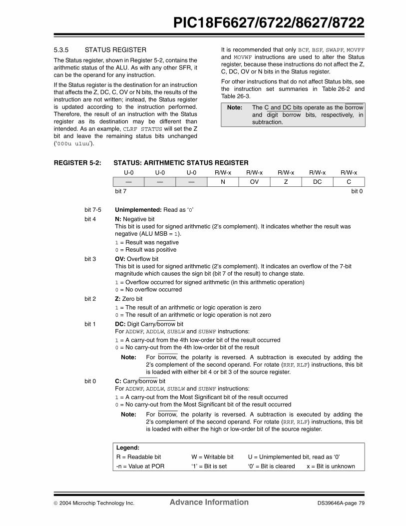
2004 Microchip Technology Inc. Advance Information DS39646A-page 79
PIC18F6627/6722/8627/8722
5.3.5 STATUS REGISTER
The Status register, shown in Register 5-2, contains thearithmetic status of the ALU. As with any other SFR, itcan be the operand for any instruction.
If the Status register is the destination for an instructionthat affects the Z, DC, C, OV or N bits, the results of theinstruction are not written; instead, the Status registeris updated according to the instruction performed.Therefore, the result of an instruction with the Statusregister as its destination may be different thanintended. As an example, CLRF STATUS will set the Zbit and leave the remaining status bits unchanged(‘000u u1uu’).
It is recommended that only BCF, BSF, SWAPF, MOVFFand MOVWF instructions are used to alter the Statusregister, because these instructions do not affect the Z,C, DC, OV or N bits in the Status register.
For other instructions that do not affect Status bits, seethe instruction set summaries in Table 26-2 andTable 26-3.
REGISTER 5-2: STATUS: ARITHMETIC STATUS REGISTER
Note: The C and DC bits operate as the borrowand digit borrow bits, respectively, insubtraction.
U-0 U-0 U-0 R/W-x R/W-x R/W-x R/W-x R/W-x
— — — N OV Z DC C
bit 7 bit 0
bit 7-5 Unimplemented: Read as ‘0’
bit 4 N: Negative bit This bit is used for signed arithmetic (2’s complement). It indicates whether the result was negative (ALU MSB = 1).
1 = Result was negative 0 = Result was positive
bit 3 OV: Overflow bit This bit is used for signed arithmetic (2’s complement). It indicates an overflow of the 7-bit magnitude which causes the sign bit (bit 7 of the result) to change state.
1 = Overflow occurred for signed arithmetic (in this arithmetic operation) 0 = No overflow occurred
bit 2 Z: Zero bit 1 = The result of an arithmetic or logic operation is zero 0 = The result of an arithmetic or logic operation is not zero
bit 1 DC: Digit Carry/borrow bit For ADDWF, ADDLW, SUBLW and SUBWF instructions:
1 = A carry-out from the 4th low-order bit of the result occurred 0 = No carry-out from the 4th low-order bit of the result
Note: For borrow, the polarity is reversed. A subtraction is executed by adding the2’s complement of the second operand. For rotate (RRF, RLF) instructions, this bitis loaded with either bit 4 or bit 3 of the source register.
bit 0 C: Carry/borrow bit For ADDWF, ADDLW, SUBLW and SUBWF instructions: 1 = A carry-out from the Most Significant bit of the result occurred 0 = No carry-out from the Most Significant bit of the result occurred
Note: For borrow, the polarity is reversed. A subtraction is executed by adding the2’s complement of the second operand. For rotate (RRF, RLF) instructions, this bitis loaded with either the high or low-order bit of the source register.
Legend:
R = Readable bit W = Writable bit U = Unimplemented bit, read as ‘0’
-n = Value at POR ‘1’ = Bit is set ‘0’ = Bit is cleared x = Bit is unknown

PIC18F6627/6722/8627/8722
DS39646A-page 80 Advance Information 2004 Microchip Technology Inc.
5.4 Data Addressing Modes
The data memory space can be addressed in severalways. For most instructions, the addressing mode isfixed. Other instructions may use up to three modes,depending on which operands are used and whether ornot the extended instruction set is enabled.
The addressing modes are:
• Inherent• Literal
• Direct• Indirect
An additional addressing mode, Indexed Literal Offset,is available when the extended instruction set isenabled (XINST configuration bit = 1). Its operation isdiscussed in greater detail in Section 5.5.1 “IndexedAddressing with Literal Offset”.
5.4.1 INHERENT AND LITERAL ADDRESSING
Many PIC18 control instructions do not need any argu-ment at all; they either perform an operation that glo-bally affects the device or they operate implicitly on oneregister. This addressing mode is known as InherentAddressing. Examples include SLEEP, RESET and DAW.
Other instructions work in a similar way but require anadditional explicit argument in the opcode. This isknown as Literal Addressing mode because theyrequire some literal value as an argument. Examplesinclude ADDLW and MOVLW, which respectively, add ormove a literal value to the W register. Other examplesinclude CALL and GOTO, which include a 20-bitprogram memory address.
5.4.2 DIRECT ADDRESSING
Direct addressing specifies all or part of the sourceand/or destination address of the operation within theopcode itself. The options are specified by thearguments accompanying the instruction.
In the core PIC18 instruction set, bit-oriented and byte-oriented instructions use some version of directaddressing by default. All of these instructions includesome 8-bit literal address as their Least SignificantByte. This address specifies either a register address inone of the banks of data RAM (Section 5.3.3 “GeneralPurpose Register File”) or a location in the AccessBank (Section 5.3.2 “Access Bank”) as the datasource for the instruction.
The Access RAM bit ‘a’ determines how the address isinterpreted. When ‘a’ is ‘1’, the contents of the BSR(Section 5.3.1 “Bank Select Register (BSR)”) areused with the address to determine the complete 12-bitaddress of the register. When ‘a’ is ‘0’, the address isinterpreted as being a register in the Access Bank.Addressing that uses the Access RAM is sometimesalso known as Direct Forced Addressing mode.
A few instructions, such as MOVFF, include the entire12-bit address (either source or destination) in theiropcodes. In these cases, the BSR is ignored entirely.
The destination of the operation’s results is determinedby the destination bit ‘d’. When ‘d’ is ‘1’, the results arestored back in the source register, overwriting its origi-nal contents. When ‘d’ is ‘0’, the results are stored inthe W register. Instructions without the ‘d’ argumenthave a destination that is implicit in the instruction; theirdestination is either the target register being operatedon or the W register.
5.4.3 INDIRECT ADDRESSING
Indirect addressing allows the user to access a locationin data memory without giving a fixed address in theinstruction. This is done by using File Select Registers(FSRs) as pointers to the locations to be read or writtento. Since the FSRs are themselves located in RAM asSpecial File Registers, they can also be directly manip-ulated under program control. This makes FSRs veryuseful in implementing data structures, such as tablesand arrays in data memory.
The registers for indirect addressing are alsoimplemented with Indirect File Operands (INDFs) thatpermit automatic manipulation of the pointer value withauto-incrementing, auto-decrementing or offsettingwith another value. This allows for efficient code, usingloops, such as the example of clearing an entire RAMbank in Example 5-5.
EXAMPLE 5-5: HOW TO CLEAR RAM (BANK 1) USING INDIRECT ADDRESSING
Note: The execution of some instructions in thecore PIC18 instruction set are changedwhen the PIC18 extended instruction set isenabled. See Section 5.5 “Data Memoryand the Extended Instruction Set” formore information.
LFSR FSR0, 100h ; NEXT CLRF POSTINC0 ; Clear INDF
; register then ; inc pointer
BTFSS FSR0H, 1 ; All done with; Bank1?
BRA NEXT ; NO, clear next CONTINUE ; YES, continue

2004 Microchip Technology Inc. Advance Information DS39646A-page 81
PIC18F6627/6722/8627/8722
5.4.3.1 FSR Registers and the INDF Operand
At the core of indirect addressing are three sets ofregisters: FSR0, FSR1 and FSR2. Each represents apair of 8-bit registers, FSRnH and FSRnL. The fourupper bits of the FSRnH register are not used so eachFSR pair holds a 12-bit value. This represents a valuethat can address the entire range of the data memoryin a linear fashion. The FSR register pairs, then, serveas pointers to data memory locations.
Indirect addressing is accomplished with a set ofIndirect File Operands, INDF0 through INDF2. Thesecan be thought of as “virtual” registers: they aremapped in the SFR space, but are not physically imple-mented. Reading or writing to a particular INDF registeractually accesses its corresponding FSR register pair.A read from INDF1, for example, reads the data at theaddress indicated by FSR1H:FSR1L. Instructions thatuse the INDF registers as operands actually use thecontents of their corresponding FSR as a pointer to theinstruction’s target. The INDF operand is just aconvenient way of using the pointer.
Because indirect addressing uses a full 12-bit address,data RAM banking is not necessary. Thus, the currentcontents of the BSR and the Access RAM bit have noeffect on determining the target address.
5.4.3.2 FSR Registers and POSTINC, POSTDEC, PREINC and PLUSW
In addition to the INDF operand, each FSR register pairalso has four additional indirect operands. Like INDF,these are “virtual” registers that cannot be indirectlyread or written to. Accessing these registers actuallyaccesses the associated FSR register pair, but alsoperforms a specific action on its stored value. They are:
• POSTDEC: accesses the FSR value, then automatically decrements it by 1 afterwards
• POSTINC: accesses the FSR value, then automatically increments it by 1 afterwards
• PREINC: increments the FSR value by 1, then uses it in the operation
• PLUSW: adds the signed value of the W register (range of -127 to 128) to that of the FSR and uses the new value in the operation.
In this context, accessing an INDF register uses thevalue in the FSR registers without changing them.Similarly, accessing a PLUSW register gives the FSRvalue offset by the value in the W register; neither valueis actually changed in the operation. Accessing theother virtual registers changes the value of the FSRregisters.
Operations on the FSRs with POSTDEC, POSTINCand PREINC affect the entire register pair; that is, roll-overs of the FSRnL register from FFh to 00h carry overto the FSRnH register. On the other hand, results ofthese operations do not change the value of any flagsin the Status register (e.g., Z, N, OV, etc.).
FIGURE 5-8: INDIRECT ADDRESSING
FSR1H:FSR1L
07
Data Memory
000h
100h
200h
300h
F00h
E00h
FFFh
Bank 0
Bank 1
Bank 2
Bank 14
Bank 15
Bank 3throughBank 13
ADDWF, INDF1, 1
07
Using an instruction with one of theindirect addressing registers as theoperand....
...uses the 12-bit address stored inthe FSR pair associated with thatregister....
...to determine the data memorylocation to be used in that operation.
In this case, the FSR1 pair containsECCh. This means the contents oflocation ECCh will be added to thatof the W register and stored back inECCh.
x x x x 1 1 1 0 1 1 0 0 1 1 0 0
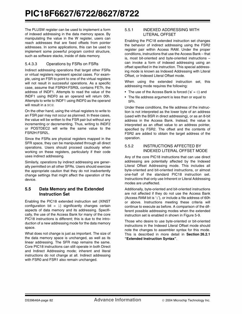
PIC18F6627/6722/8627/8722
DS39646A-page 82 Advance Information 2004 Microchip Technology Inc.
The PLUSW register can be used to implement a formof indexed addressing in the data memory space. Bymanipulating the value in the W register, users canreach addresses that are fixed offsets from pointeraddresses. In some applications, this can be used toimplement some powerful program control structure,such as software stacks, inside of data memory.
5.4.3.3 Operations by FSRs on FSRs
Indirect addressing operations that target other FSRsor virtual registers represent special cases. For exam-ple, using an FSR to point to one of the virtual registerswill not result in successful operations. As a specificcase, assume that FSR0H:FSR0L contains FE7h, theaddress of INDF1. Attempts to read the value of theINDF1 using INDF0 as an operand will return 00h.Attempts to write to INDF1 using INDF0 as the operandwill result in a NOP.
On the other hand, using the virtual registers to write toan FSR pair may not occur as planned. In these cases,the value will be written to the FSR pair but without anyincrementing or decrementing. Thus, writing to INDF2or POSTDEC2 will write the same value to theFSR2H:FSR2L.
Since the FSRs are physical registers mapped in theSFR space, they can be manipulated through all directoperations. Users should proceed cautiously whenworking on these registers, particularly if their codeuses indirect addressing.
Similarly, operations by indirect addressing are gener-ally permitted on all other SFRs. Users should exercisethe appropriate caution that they do not inadvertentlychange settings that might affect the operation of thedevice.
5.5 Data Memory and the Extended Instruction Set
Enabling the PIC18 extended instruction set (XINSTconfiguration bit = 1) significantly changes certainaspects of data memory and its addressing. Specifi-cally, the use of the Access Bank for many of the corePIC18 instructions is different; this is due to the intro-duction of a new addressing mode for the data memoryspace.
What does not change is just as important. The size ofthe data memory space is unchanged, as well as itslinear addressing. The SFR map remains the same.Core PIC18 instructions can still operate in both Directand Indirect Addressing mode; inherent and literalinstructions do not change at all. Indirect addressingwith FSR0 and FSR1 also remain unchanged.
5.5.1 INDEXED ADDRESSING WITH LITERAL OFFSET
Enabling the PIC18 extended instruction set changesthe behavior of indirect addressing using the FSR2register pair within Access RAM. Under the properconditions, instructions that use the Access Bank – thatis, most bit-oriented and byte-oriented instructions –can invoke a form of indexed addressing using anoffset specified in the instruction. This special address-ing mode is known as Indexed Addressing with LiteralOffset, or Indexed Literal Offset mode.
When using the extended instruction set, thisaddressing mode requires the following:
• The use of the Access Bank is forced (‘a’ = 0) and
• The file address argument is less than or equal to 5Fh.
Under these conditions, the file address of the instruc-tion is not interpreted as the lower byte of an address(used with the BSR in direct addressing), or as an 8-bitaddress in the Access Bank. Instead, the value isinterpreted as an offset value to an address pointer,specified by FSR2. The offset and the contents ofFSR2 are added to obtain the target address of theoperation.
5.5.2 INSTRUCTIONS AFFECTED BY INDEXED LITERAL OFFSET MODE
Any of the core PIC18 instructions that can use directaddressing are potentially affected by the IndexedLiteral Offset Addressing mode. This includes allbyte-oriented and bit-oriented instructions, or almostone-half of the standard PIC18 instruction set.Instructions that only use Inherent or Literal Addressingmodes are unaffected.
Additionally, byte-oriented and bit-oriented instructionsare not affected if they do not use the Access Bank(Access RAM bit is ‘1’), or include a file address of 60hor above. Instructions meeting these criteria willcontinue to execute as before. A comparison of the dif-ferent possible addressing modes when the extendedinstruction set is enabled in shown in Figure 5-9.
Those who desire to use byte-oriented or bit-orientedinstructions in the Indexed Literal Offset mode shouldnote the changes to assembler syntax for this mode.This is described in more detail in Section 26.2.1“Extended Instruction Syntax”.
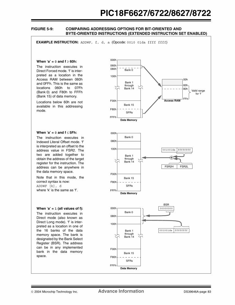
2004 Microchip Technology Inc. Advance Information DS39646A-page 83
PIC18F6627/6722/8627/8722
FIGURE 5-9: COMPARING ADDRESSING OPTIONS FOR BIT-ORIENTED AND BYTE-ORIENTED INSTRUCTIONS (EXTENDED INSTRUCTION SET ENABLED)
EXAMPLE INSTRUCTION: ADDWF, f, d, a (Opcode: 0010 01da ffff ffff)
When ‘a’ = 0 and f ≥ 60h:
The instruction executes inDirect Forced mode. ‘f’ is inter-preted as a location in theAccess RAM between 060hand 0FFh. This is the same aslocations 060h to 07Fh(Bank 0) and F80h to FFFh(Bank 15) of data memory.
Locations below 60h are notavailable in this addressingmode.
When ‘a’ = 0 and f ≤ 5Fh:The instruction executes inIndexed Literal Offset mode. ‘f’is interpreted as an offset to theaddress value in FSR2. Thetwo are added together toobtain the address of the targetregister for the instruction. Theaddress can be anywhere inthe data memory space.
Note that in this mode, thecorrect syntax is now:ADDWF [k], dwhere ‘k’ is the same as ‘f’.
When ‘a’ = 1 (all values of f):The instruction executes inDirect mode (also known asDirect Long mode). ‘f’ is inter-preted as a location in one ofthe 16 banks of the datamemory space. The bank isdesignated by the Bank SelectRegister (BSR). The addresscan be in any implementedbank in the data memoryspace.
000h
060h
100h
F00h
F80h
FFFh
Valid range
00h
60h80h
FFh
Data Memory
Access RAM
Bank 0
Bank 1throughBank 14
Bank 15
SFRs
000h
080h
100h
F00h
F80h
FFFhData Memory
Bank 0
Bank 1throughBank 14
Bank 15
SFRs
FSR2H FSR2L
ffffffff001001da
ffffffff001001da
000h
080h
100h
F00h
F80h
FFFhData Memory
Bank 0
Bank 1throughBank 14
Bank 15
SFRs
for ‘f’
BSR00000000
080h

PIC18F6627/6722/8627/8722
DS39646A-page 84 Advance Information 2004 Microchip Technology Inc.
5.5.3 MAPPING THE ACCESS BANK IN INDEXED LITERAL OFFSET MODE
The use of Indexed Literal Offset Addressing modeeffectively changes how the first 96 locations of AccessRAM (00h to 5Fh) are mapped. Rather than containingjust the contents of the bottom half of Bank 0, this modemaps the contents from Bank 0 and a user defined“window” that can be located anywhere in the datamemory space. The value of FSR2 establishes thelower boundary of the addresses mapped into thewindow, while the upper boundary is defined by FSR2plus 95 (5Fh). Addresses in the Access RAM above5Fh are mapped as previously described (seeSection 5.3.2 “Access Bank”). An example of AccessBank remapping in this addressing mode is shown inFigure 5-10.
Remapping of the Access Bank applies only to opera-tions using the Indexed Literal Offset mode. Operationsthat use the BSR (Access RAM bit is ‘1’) will continueto use direct addressing as before.
5.6 PIC18 Instruction Execution and the Extended Instruction Set
Enabling the extended instruction set adds eightadditional commands to the existing PIC18 instructionset. These instructions are executed as described inSection 26.2 “Extended Instruction Set”.
FIGURE 5-10: REMAPPING THE ACCESS BANK WITH INDEXED LITERAL OFFSET ADDRESSING
Data Memory
000h
100h
200h
F80h
F00h
FFFh
Bank 1
Bank 15
Bank 2throughBank 14
SFRs
05FhADDWF f, d, a
FSR2H:FSR2L = 120h
Locations in the regionfrom the FSR2 pointer(120h) to the pointer plus05Fh (17Fh) are mappedto the bottom of theAccess RAM (000h-05Fh).
Locations in Bank 0 from060h to 07Fh are mapped,as usual, to the middle halfof the Access Bank.
Special File Registers atF80h through FFFh aremapped to 80h throughFFh, as usual.
Bank 0 addresses below5Fh can still be addressedby using the BSR.
Access Bank
00h
80h
FFh
7Fh
Bank 0
SFRs
Bank 1 “Window”
Bank 0
Bank 0
Window
Example Situation:
07Fh
120h17Fh
5Fh
Bank 1

2004 Microchip Technology Inc. Advance Information DS39646A-page 85
PIC18F6627/6722/8627/8722
6.0 FLASH PROGRAM MEMORY
The Flash program memory is readable, writable anderasable during normal operation over the entire VDD
range.
A read from program memory is executed on one byteat a time. A write to program memory is executed onblocks of 64 bytes at a time. Program memory iserased in blocks of 64 bytes at a time. A bulk eraseoperation may not be issued from user code.
Writing or erasing program memory will ceaseinstruction fetches until the operation is complete. Theprogram memory cannot be accessed during the writeor erase, therefore, code cannot execute. An internalprogramming timer terminates program memory writesand erases.
A value written to program memory does not need to bea valid instruction. Executing a program memorylocation that forms an invalid instruction results in aNOP.
6.1 Table Reads and Table Writes
In order to read and write program memory, there aretwo operations that allow the processor to move bytesbetween the program memory space and the data RAM:
• Table Read (TBLRD)• Table Write (TBLWT)
The program memory space is 16 bits wide, while thedata RAM space is 8 bits wide. Table reads and tablewrites move data between these two memory spacesthrough an 8-bit register (TABLAT).
Table read operations retrieve data from programmemory and place it into the data RAM space.Figure 6-1 shows the operation of a table read withprogram memory and data RAM.
Table write operations store data from the data memoryspace into holding registers in program memory. Theprocedure to write the contents of the holding registersinto program memory is detailed in Section 6.5 “Writingto Flash Program Memory”. Figure 6-2 shows theoperation of a table write with program memory and dataRAM.
Table operations work with byte entities. A table blockcontaining data, rather than program instructions, is notrequired to be word aligned. Therefore, a table block canstart and end at any byte address. If a table write is beingused to write executable code into program memory,program instructions will need to be word aligned.
FIGURE 6-1: TABLE READ OPERATION
Table Pointer(1)
Table Latch (8-bit)Program Memory
TBLPTRH TBLPTRLTABLAT
TBLPTRU
Instruction: TBLRD*
Note 1: Table Pointer register points to a byte in program memory.
Program Memory(TBLPTR)

PIC18F6627/6722/8627/8722
DS39646A-page 86 Advance Information 2004 Microchip Technology Inc.
FIGURE 6-2: TABLE WRITE OPERATION
6.2 Control Registers
Several control registers are used in conjunction withthe TBLRD and TBLWT instructions. These include the:
• EECON1 register
• EECON2 register• TABLAT register• TBLPTR registers
6.2.1 EECON1 AND EECON2 REGISTERS
The EECON1 register (Register 6-1) is the controlregister for memory accesses. The EECON2 register isnot a physical register; it is used exclusively in thememory write and erase sequences. ReadingEECON2 will read all ‘0’s.
The EEPGD control bit determines if the access will bea program or data EEPROM memory access. Whenclear, any subsequent operations will operate on thedata EEPROM memory. When set, any subsequentoperations will operate on the program memory.
The CFGS control bit determines if the access will beto the configuration/calibration registers or to programmemory/data EEPROM memory. When set,subsequent operations will operate on configurationregisters regardless of EEPGD (see Section 25.0“Special Features of the CPU”). When clear, memoryselection access is determined by EEPGD.
The FREE bit, when set, will allow a program memoryerase operation. When FREE is set, the eraseoperation is initiated on the next WR command. WhenFREE is clear, only writes are enabled.
The WREN bit, when set, will allow a write operation.On power-up, the WREN bit is clear. The WRERR bit isset in hardware when the WR bit is set and clearedwhen the internal programming timer expires and thewrite operation is complete.
The WR control bit initiates write operations. The bitcannot be cleared, only set, in software; it is cleared inhardware at the completion of the write operation.
Table Pointer(1)Table Latch (8-bit)
TBLPTRH TBLPTRL TABLAT
Program Memory(TBLPTR)
TBLPTRU
Instruction: TBLWT*
Note 1: Table Pointer actually points to one of 64 holding registers, the address of which is determined byTBLPTRL<5:0>. The process for physically writing data to the program memory array is discussed inSection 6.5 “Writing to Flash Program Memory”.
Holding Registers Program Memory
Note: During normal operation, the WRERR isread as ‘1’. This can indicate that a writeoperation was prematurely terminated bya Reset, or a write operation wasattempted improperly.
Note: The EEIF interrupt flag bit (PIR2<4>) is setwhen the write is complete. It must becleared in software.

2004 Microchip Technology Inc. Advance Information DS39646A-page 87
PIC18F6627/6722/8627/8722
REGISTER 6-1: EECON1: EEPROM CONTROL REGISTER 1 R/W-x R/W-x U-0 R/W-0 R/W-x R/W-0 R/S-0 R/S-0
EEPGD CFGS — FREE WRERR WREN WR RD
bit 7 bit 0
bit 7 EEPGD: Flash Program or Data EEPROM Memory Select bit1 = Access Flash program memory0 = Access data EEPROM memory
bit 6 CFGS: Flash Program/Data EEPROM or Configuration Select bit
1 = Access Configuration registers0 = Access Flash program or data EEPROM memory
bit 5 Unimplemented: Read as ‘0’
bit 4 FREE: Flash Row Erase Enable bit1 = Erase the program memory row addressed by TBLPTR on the next WR command
(cleared by completion of erase operation)0 = Perform write only
bit 3 WRERR: Flash Program/Data EEPROM Error Flag bit1 = A write operation is prematurely terminated (any Reset during self-timed programming in
normal operation, or an improper write attempt)0 = The write operation completed
Note: When a WRERR occurs, the EEPGD and CFGS bits are not cleared. This allows tracing of the error condition.
bit 2 WREN: Flash Program/Data EEPROM Write Enable bit1 = Allows write cycles to Flash program/data EEPROM0 = Inhibits write cycles to Flash program/data EEPROM
bit 1 WR: Write Control bit1 = Initiates a data EEPROM erase/write cycle or a program memory erase cycle or write cycle.
(The operation is self-timed and the bit is cleared by hardware once write is complete. The WR bit can only be set (not cleared) in software.)
0 = Write cycle to the EEPROM is complete
bit 0 RD: Read Control bit1 = Initiates an EEPROM read (Read takes one cycle. RD is cleared in hardware. The RD bit can
only be set (not cleared) in software. RD bit cannot be set when EEPGD = 1 or CFGS = 1.)0 = Does not initiate an EEPROM read
Legend:
R = Readable bit W = Writable bit
S = Bit can be set by software, but not cleared U = Unimplemented bit, read as ‘0’
-n = Value at POR ‘1’ = Bit is set ‘0’ = Bit is cleared x = Bit is unknown

PIC18F6627/6722/8627/8722
DS39646A-page 88 Advance Information 2004 Microchip Technology Inc.
6.2.2 TABLAT – TABLE LATCH REGISTER
The Table Latch (TABLAT) is an 8-bit register mappedinto the SFR space. The Table Latch register is used tohold 8-bit data during data transfers between programmemory and data RAM.
6.2.3 TBLPTR – TABLE POINTER REGISTER
The Table Pointer (TBLPTR) register addresses a bytewithin the program memory. The TBLPTR is comprisedof three SFR registers: Table Pointer Upper Byte, TablePointer High Byte and Table Pointer Low Byte(TBLPTRU:TBLPTRH:TBLPTRL). These three regis-ters join to form a 22-bit wide pointer. The low-order21 bits allow the device to address up to 2 Mbytes ofprogram memory space. The 22nd bit allows access tothe device ID, the user ID and the configuration bits.
The Table Pointer register, TBLPTR, is used by theTBLRD and TBLWT instructions. These instructions canupdate the TBLPTR in one of four ways based on thetable operation. These operations are shown inTable 6-1. These operations on the TBLPTR only affectthe low-order 21 bits.
6.2.4 TABLE POINTER BOUNDARIES
TBLPTR is used in reads, writes and erases of theFlash program memory.
When a TBLRD is executed, all 22 bits of the TBLPTRdetermine which byte is read from program memoryinto TABLAT.
When a TBLWT is executed, the six LSbs of the TablePointer register (TBLPTR<5:0>) determine which of the64 program memory holding registers is written to.When the timed write to program memory begins (viathe WR bit), the 16 MSbs of the TBLPTR(TBLPTR<21:6>) determine which program memoryblock of 64 bytes is written to. For more detail, seeSection 6.5 “Writing to Flash Program Memory”.
When an erase of program memory is executed, the16 MSbs of the Table Pointer register (TBLPTR<21:6>)point to the 64-byte block that will be erased. The LeastSignificant bits (TBLPTR<5:0>) are ignored.
Figure 6-3 describes the relevant boundaries ofTBLPTR based on Flash program memory operations.
TABLE 6-1: TABLE POINTER OPERATIONS WITH TBLRD AND TBLWT INSTRUCTIONS
FIGURE 6-3: TABLE POINTER BOUNDARIES BASED ON OPERATION
Example Operation on Table Pointer
TBLRD*TBLWT*
TBLPTR is not modified
TBLRD*+TBLWT*+
TBLPTR is incremented after the read/write
TBLRD*-TBLWT*-
TBLPTR is decremented after the read/write
TBLRD+*TBLWT+*
TBLPTR is incremented before the read/write
21 16 15 8 7 0
TABLE ERASE/WRITE TABLE WRITE
TABLE READ – TBLPTR<21:0>
TBLPTRLTBLPTRHTBLPTRU
TBLPTR<5:0>TBLPTR<21:6>

2004 Microchip Technology Inc. Advance Information DS39646A-page 89
PIC18F6627/6722/8627/8722
6.3 Reading the Flash Program Memory
The TBLRD instruction is used to retrieve data fromprogram memory and places it into data RAM. Tablereads from program memory are performed one byte ata time.
TBLPTR points to a byte address in program space.Executing TBLRD places the byte pointed to intoTABLAT. In addition, TBLPTR can be modifiedautomatically for the next table read operation.
The internal program memory is typically organized bywords. The Least Significant bit of the address selectsbetween the high and low bytes of the word. Figure 6-4shows the interface between the internal programmemory and the TABLAT.
FIGURE 6-4: READS FROM FLASH PROGRAM MEMORY
EXAMPLE 6-1: READING A FLASH PROGRAM MEMORY WORD
(Even Byte Address)
Program Memory
(Odd Byte Address)
TBLRDTABLAT
TBLPTR = xxxxx1
FETCHInstruction Register
(IR) Read Register
TBLPTR = xxxxx0
MOVLW CODE_ADDR_UPPER ; Load TBLPTR with the baseMOVWF TBLPTRU ; address of the wordMOVLW CODE_ADDR_HIGHMOVWF TBLPTRHMOVLW CODE_ADDR_LOWMOVWF TBLPTRL
READ_WORDTBLRD*+ ; read into TABLAT and incrementMOVF TABLAT, W ; get dataMOVWF WORD_EVENTBLRD*+ ; read into TABLAT and incrementMOVFW TABLAT, W ; get dataMOVF WORD_ODD

PIC18F6627/6722/8627/8722
DS39646A-page 90 Advance Information 2004 Microchip Technology Inc.
6.4 Erasing Flash Program Memory
The minimum erase block is 32 words or 64 bytes. Onlythrough the use of an external programmer, or throughICSP control, can larger blocks of program memory bebulk erased. Word erase in the Flash array is notsupported.
When initiating an erase sequence from the micro-controller itself, a block of 64 bytes of program memoryis erased. The Most Significant 16 bits of theTBLPTR<21:6> point to the block being erased.TBLPTR<5:0> are ignored.
The EECON1 register commands the erase operation.The EEPGD bit must be set to point to the Flash pro-gram memory. The WREN bit must be set to enablewrite operations. The FREE bit is set to select an eraseoperation.
For protection, the write initiate sequence for EECON2must be used.
A long write is necessary for erasing the internal Flash.Instruction execution is halted while in a long writecycle. The long write will be terminated by the internalprogramming timer.
6.4.1 FLASH PROGRAM MEMORY ERASE SEQUENCE
The sequence of events for erasing a block of internalprogram memory location is:
1. Load Table Pointer register with address of rowbeing erased.
2. Set the EECON1 register for the erase operation:• set EEPGD bit to point to program memory;
• clear the CFGS bit to access program memory;• set WREN bit to enable writes; • set FREE bit to enable the erase.
3. Disable interrupts.4. Write 55h to EECON2.5. Write 0AAh to EECON2.
6. Set the WR bit. This will begin the row erasecycle.
7. The CPU will stall for duration of the erase forTIW (see parameter D133A).
8. Re-enable interrupts.
EXAMPLE 6-2: ERASING A FLASH PROGRAM MEMORY ROW MOVLW CODE_ADDR_UPPER ; load TBLPTR with the baseMOVWF TBLPTRU ; address of the memory blockMOVLW CODE_ADDR_HIGHMOVWF TBLPTRH MOVLW CODE_ADDR_LOWMOVWF TBLPTRL
ERASE_ROW BSF EECON1, EEPGD ; point to Flash program memoryBCF EECON1, CFGS ; access Flash program memoryBSF EECON1, WREN ; enable write to memoryBSF EECON1, FREE ; enable Row Erase operationBCF INTCON, GIE ; disable interrupts
Required MOVLW 55hSequence MOVWF EECON2 ; write 55h
MOVLW 0AAhMOVWF EECON2 ; write 0AAhBSF EECON1, WR ; start erase (CPU stall)BSF INTCON, GIE ; re-enable interrupts

2004 Microchip Technology Inc. Advance Information DS39646A-page 91
PIC18F6627/6722/8627/8722
6.5 Writing to Flash Program Memory
The minimum programming block is 32 words or64 bytes. Word or byte programming is not supported.
Table writes are used internally to load the holdingregisters needed to program the Flash memory. Thereare 64 holding registers used by the table writes forprogramming.
Since the Table Latch (TABLAT) is only a single byte,the TBLWT instruction may need to be executed 64times for each programming operation. All of the tablewrite operations will essentially be short writes becauseonly the holding registers are written. At the end ofupdating the 64 holding registers, the EECON1 registermust be written to in order to start the programmingoperation with a long write.
The long write is necessary for programming the inter-nal Flash. Instruction execution is halted while in a longwrite cycle. The long write will be terminated by theinternal programming timer.
The EEPROM on-chip timer controls the write time.The write/erase voltages are generated by an on-chipcharge pump, rated to operate over the voltage rangeof the device.
FIGURE 6-5: TABLE WRITES TO FLASH PROGRAM MEMORY
6.5.1 FLASH PROGRAM MEMORY WRITE SEQUENCE
The sequence of events for programming an internalprogram memory location should be:
1. Read 64 bytes into RAM.2. Update data values in RAM as necessary.3. Load Table Pointer register with address being
erased.4. Execute the row erase procedure.5. Load Table Pointer register with address of first
byte being written.6. Write the 64 bytes into the holding registers with
auto-increment.7. Set the EECON1 register for the write operation:
• set EEPGD bit to point to program memory;• clear the CFGS bit to access program memory;• set WREN to enable byte writes.
8. Disable interrupts.9. Write 55h to EECON2.10. Write 0AAh to EECON2.11. Set the WR bit. This will begin the write cycle.12. The CPU will stall for duration of the write for TIW
(see parameter D133A).13. Re-enable interrupts.14. Verify the memory (table read).
An example of the required code is shown inExample 6-3 on the following page.
Note: The default value of the holding registers ondevice Resets and after write operations isFFh. A write of FFh to a holding registerdoes not modify that byte. This means thatindividual bytes of program memory may bemodified, provided that the change does notattempt to change any bit from a ‘0’ to a ‘1’.When modifying individual bytes, it is notnecessary to load all 64 holding registersbefore executing a write operation.
TABLAT
TBLPTR = xxxx3FTBLPTR = xxxxx1TBLPTR = xxxxx0
Write Register
TBLPTR = xxxxx2
Program Memory
Holding Register Holding Register Holding Register Holding Register
8 8 8 8
Note: Before setting the WR bit, the TablePointer address needs to be within theintended address range of the 64 bytes inthe holding register.

PIC18F6627/6722/8627/8722
DS39646A-page 92 Advance Information 2004 Microchip Technology Inc.
EXAMPLE 6-3: WRITING TO FLASH PROGRAM MEMORYMOVLW D'64 ; number of bytes in erase blockMOVWF COUNTERMOVLW BUFFER_ADDR_HIGH ; point to bufferMOVWF FSR0HMOVLW BUFFER_ADDR_LOWMOVWF FSR0LMOVLW CODE_ADDR_UPPER ; Load TBLPTR with the baseMOVWF TBLPTRU ; address of the memory blockMOVLW CODE_ADDR_HIGHMOVWF TBLPTRHMOVLW CODE_ADDR_LOWMOVWF TBLPTRL
READ_BLOCKTBLRD*+ ; read into TABLAT, and incMOVF TABLAT, W ; get dataMOVWF POSTINC0 ; store dataDECFSZ COUNTER ; done?BRA READ_BLOCK ; repeat
MODIFY_WORDMOVLW DATA_ADDR_HIGH ; point to bufferMOVWF FSR0HMOVLW DATA_ADDR_LOWMOVWF FSR0LMOVLW NEW_DATA_LOW ; update buffer wordMOVWF POSTINC0MOVLW NEW_DATA_HIGHMOVWF INDF0
ERASE_BLOCKMOVLW CODE_ADDR_UPPER ; load TBLPTR with the baseMOVWF TBLPTRU ; address of the memory blockMOVLW CODE_ADDR_HIGHMOVWF TBLPTRH MOVLW CODE_ADDR_LOWMOVWF TBLPTRL BSF EECON1, EEPGD ; point to Flash program memoryBCF EECON1, CFGS ; access Flash program memoryBSF EECON1, WREN ; enable write to memoryBSF EECON1, FREE ; enable Row Erase operationBCF INTCON, GIE ; disable interruptsMOVLW 55h
Required MOVWF EECON2 ; write 55hSequence MOVLW 0AAh
MOVWF EECON2 ; write 0AAhBSF EECON1, WR ; start erase (CPU stall)BSF INTCON, GIE ; re-enable interruptsTBLRD*- ; dummy read decrementMOVLW BUFFER_ADDR_HIGH ; point to bufferMOVWF FSR0HMOVLW BUFFER_ADDR_LOWMOVWF FSR0L
WRITE_BUFFER_BACKMOVLW D’64 ; number of bytes in holding registerMOVWF COUNTER
WRITE_BYTE_TO_HREGSMOVFF POSTINC0, WREG ; get low byte of buffer dataMOVWF TABLAT ; present data to table latchTBLWT+* ; write data, perform a short write
; to internal TBLWT holding register.DECFSZ COUNTER ; loop until buffers are fullBRA WRITE_WORD_TO_HREGS

2004 Microchip Technology Inc. Advance Information DS39646A-page 93
PIC18F6627/6722/8627/8722
EXAMPLE 6-3: WRITING TO FLASH PROGRAM MEMORY (CONTINUED)
6.5.2 WRITE VERIFY
Depending on the application, good programmingpractice may dictate that the value written to thememory should be verified against the original value.This should be used in applications where excessivewrites can stress bits near the specification limit.
6.5.3 UNEXPECTED TERMINATION OF WRITE OPERATION
If a write is terminated by an unplanned event, such asloss of power or an unexpected Reset, the memorylocation just programmed should be verified and repro-grammed if needed. If the write operation is interruptedby a MCLR Reset or a WDT Time-out Reset duringnormal operation, the user can check the WRERR bitand rewrite the location(s) as needed.
6.5.4 PROTECTION AGAINST SPURIOUS WRITES
To protect against spurious writes to Flash programmemory, the write initiate sequence must also befollowed. See Section 25.0 “Special Features of theCPU” for more detail.
6.6 Flash Program Operation During Code Protection
See Section 25.5 “Program Verification and CodeProtection” for details on code protection of Flashprogram memory.
TABLE 6-2: REGISTERS ASSOCIATED WITH PROGRAM FLASH MEMORY
PROGRAM_MEMORYBSF EECON1, EEPGD ; point to Flash program memoryBCF EECON1, CFGS ; access Flash program memoryBSF EECON1, WREN ; enable write to memoryBCF INTCON, GIE ; disable interruptsMOVLW 55h
Required MOVWF EECON2 ; write 55hSequence MOVLW 0AAh
MOVWF EECON2 ; write 0AAhBSF EECON1, WR ; start program (CPU stall)BSF INTCON, GIE ; re-enable interruptsBCF EECON1, WREN ; disable write to memory
Name Bit 7 Bit 6 Bit 5 Bit 4 Bit 3 Bit 2 Bit 1 Bit 0Reset
Values on page
TBLPTRU — — bit 21 Program Memory Table Pointer Upper Byte (TBLPTR<20:16>) 57
TBPLTRH Program Memory Table Pointer High Byte (TBLPTR<15:8>) 57
TBLPTRL Program Memory Table Pointer Low Byte (TBLPTR<7:0>) 57
TABLAT Program Memory Table Latch 57
INTCON GIE/GIEH PEIE/GIEL TMR0IE INT0IE RBIE TMR0IF INT0IF RBIF 57
EECON2 EEPROM Control Register 2 (not a physical register) 59
EECON1 EEPGD CFGS — FREE WRERR WREN WR RD 59
IPR2 OSCFIP CMIP — EEIP BCL1IP HLVDIP TMR3IP CCP2IP 60
PIR2 OSCFIF CMIF — EEIF BCL1IF HLVDIF TMR3IF CCP2IF 60
PIE2 OSCFIE CMIE — EEIE BCL1IE HLVDIE TMR3IE CCP2IE 60
Legend: — = unimplemented, read as ‘0’. Shaded cells are not used during Flash/EEPROM access.

PIC18F6627/6722/8627/8722
DS39646A-page 94 Advance Information 2004 Microchip Technology Inc.
NOTES:

2004 Microchip Technology Inc. Advance Information DS39646A-page 95
PIC18F6627/6722/8627/8722
7.0 EXTERNAL MEMORY BUS
The External Memory Bus allows the device to accessexternal memory devices (such as Flash, EPROM,SRAM, etc.) as program or data memory. It supportsboth 8-bit and 16-bit data-width modes, and fouraddress widths from 8 to 20 bits.
The bus is implemented with 28 pins, multiplexedacross four I/O ports. Three ports (PORTD, PORTEand PORTH) are multiplexed with the address/data busfor a total of 20 available lines, while PORTJ ismultiplexed with the bus control signals.
A list of the pins and their functions is provided inTable 7-1.
TABLE 7-1: PIC18F8627/8722 EXTERNAL BUS - I/O PORT FUNCTIONS
Note: The External Memory Bus is not imple-mented on PIC18F6627 and PIC18F6722(64-pin) devices.
Name Port Bit External Memory Bus Function
RD0/AD0 PORTD 0 Address bit 0 or Data bit 0
RD1/AD1 PORTD 1 Address bit 1 or Data bit 1
RD2/AD2 PORTD 2 Address bit 2 or Data bit 2
RD3/AD3 PORTD 3 Address bit 3 or Data bit 3
RD4/AD4 PORTD 4 Address bit 4 or Data bit 4
RD5/AD5 PORTD 5 Address bit 5 or Data bit 5
RD6/AD6 PORTD 6 Address bit 6 or Data bit 6
RD7/AD7 PORTD 7 Address bit 7 or Data bit 7
RE0/AD8 PORTE 0 Address bit 8 or Data bit 8
RE1/AD9 PORTE 1 Address bit 9 or Data bit 9
RE2/AD10 PORTE 2 Address bit 10 or Data bit 10
RE3/AD11 PORTE 3 Address bit 11 or Data bit 11
RE4/AD12 PORTE 4 Address bit 12 or Data bit 12
RE5/AD13 PORTE 5 Address bit 13 or Data bit 13
RE6/AD14 PORTE 6 Address bit 14 or Data bit 14
RE7/AD15 PORTE 7 Address bit 15 or Data bit 15
RH0/A16 PORTH 0 Address bit 16
RH1/A17 PORTH 1 Address bit 17
RH2/A18 PORTH 2 Address bit 18
RH3/A19 PORTH 3 Address bit 19
RJ0/ALE PORTJ 0 Address Latch Enable (ALE) Control pin
RJ1/OE PORTJ 1 Output Enable (OE) Control pin
RJ2/WRL PORTJ 2 Write Low (WRL) Control pin
RJ3/WRH PORTJ 3 Write High (WRH) Control pin
RJ4/BA0 PORTJ 4 Byte Address bit 0 (BA0)
RJ5/CE PORTJ 5 Chip Enable (CE) Control pin
RJ6/LB PORTJ 6 Lower Byte Enable (LB) Control pin
RJ7/UB PORTJ 7 Upper Byte Enable (UB) Control pin
Note: For the sake of clarity, only I/O port and external bus assignments are shown here. One or more additionalmultiplexed features may be available on some pins.

PIC18F6627/6722/8627/8722
DS39646A-page 96 Advance Information 2004 Microchip Technology Inc.
7.1 External Memory Bus Control
The operation of the interface is controlled by theMEMCON register (Register 7-1). This register isavailable in all program memory operating modesexcept Microcontroller mode. In this mode, the registeris disabled and cannot be written to.
The EBDIS bit (MEMCON<7>) controls the operationof the bus and related port functions. Clearing EBDISenables the interface and disables the I/O functions ofthe ports, as well as any other functions multiplexed tothose pins. Setting the bit enables the I/O ports andother functions, but allows the interface to overrideeverything else on the pins when an external memoryoperation is required. By default, the external bus isalways enabled and disables all other I/O.
The operation of the EBDIS bit is also influenced by theprogram memory mode being used. This is discussedin more detail in Section 7.4 “Program MemoryModes and the External Memory Bus”.
The WAIT bits allow for the addition of wait states toexternal memory operations. The use of these bits isdiscussed in Section 7.3 “Wait States”.
The WM bits select the particular operating mode usedwhen the bus is operating in 16-bit data-width mode.These are discussed in more detail in Section 7.5“16-bit Data Width Modes”. These bits have no effectwhen an 8-bit data-width mode is selected.
REGISTER 7-1: MEMCON: EXTERNAL MEMORY BUS CONTROL REGISTER R/W-0 U-0 R/W-0 R/W-0 U-0 U-0 R/W-0 R/W-0
EBDIS — WAIT1 WAIT0 — — WM1 WM0
bit7 bit0
bit 7 EBDIS: External Bus Disable bit
1 = External bus enabled when microcontroller accesses external memory; otherwise all external bus drivers are mapped as I/O ports
0 = External bus always enabled, I/O ports are disabled
bit 6 Unimplemented: Read as ‘0’
bit 5-4 WAIT1:WAIT0: Table Reads and Writes Bus Cycle Wait Count bits
11 = Table reads and writes will wait 0 TCY
10 = Table reads and writes will wait 1 TCY
01 = Table reads and writes will wait 2 TCY
00 = Table reads and writes will wait 3 TCY
bit 3-2 Unimplemented: Read as ‘0’
bit 1-0 WM1:WM0: TBLWT Operation with 16-bit Data Bus Width Select bits
1X = Word Write mode: TABLAT0 and TABLAT1 word output, WRH active when TABLAT1 written
01 = Byte Select mode: TABLAT data copied on both MS and LS Byte, WRH and (UB or LB) will activate
00 = Byte Write mode: TABLAT data copied on both MS and LS Byte, WRH or WRL will activate
Legend:
R = Readable bit W = Writable bit U = Unimplemented bit, read as ‘0’
- n = Value at POR ‘1’ = Bit is set ‘0’ = Bit is cleared x = Bit is unknown
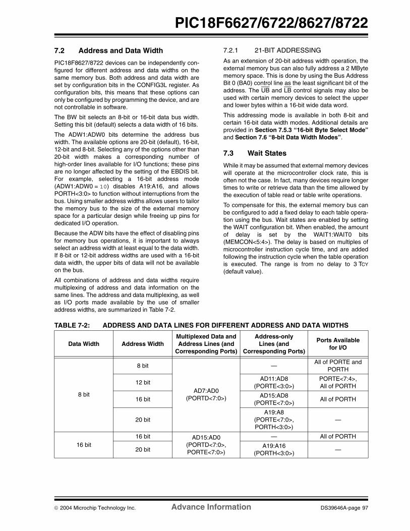
2004 Microchip Technology Inc. Advance Information DS39646A-page 97
PIC18F6627/6722/8627/8722
7.2 Address and Data Width
PIC18F8627/8722 devices can be independently con-figured for different address and data widths on thesame memory bus. Both address and data width areset by configuration bits in the CONFIG3L register. Asconfiguration bits, this means that these options canonly be configured by programming the device, and arenot controllable in software.
The BW bit selects an 8-bit or 16-bit data bus width.Setting this bit (default) selects a data width of 16 bits.
The ADW1:ADW0 bits determine the address buswidth. The available options are 20-bit (default), 16-bit,12-bit and 8-bit. Selecting any of the options other than20-bit width makes a corresponding number ofhigh-order lines available for I/O functions; these pinsare no longer affected by the setting of the EBDIS bit.For example, selecting a 16-bit address mode(ADW1:ADW0 = 10) disables A19:A16, and allowsPORTH<3:0> to function without interruptions from thebus. Using smaller address widths allows users to tailorthe memory bus to the size of the external memoryspace for a particular design while freeing up pins fordedicated I/O operation.
Because the ADW bits have the effect of disabling pinsfor memory bus operations, it is important to alwaysselect an address width at least equal to the data width.If 8-bit or 12-bit address widths are used with a 16-bitdata width, the upper bits of data will not be availableon the bus.
All combinations of address and data widths requiremultiplexing of address and data information on thesame lines. The address and data multiplexing, as wellas I/O ports made available by the use of smalleraddress widths, are summarized in Table 7-2.
7.2.1 21-BIT ADDRESSING
As an extension of 20-bit address width operation, theexternal memory bus can also fully address a 2 MBytememory space. This is done by using the Bus AddressBit 0 (BA0) control line as the least significant bit of theaddress. The UB and LB control signals may also beused with certain memory devices to select the upperand lower bytes within a 16-bit wide data word.
This addressing mode is available in both 8-bit andcertain 16-bit data width modes. Additional details areprovided in Section 7.5.3 “16-bit Byte Select Mode”and Section 7.6 “8-bit Data Width Modes”.
7.3 Wait States
While it may be assumed that external memory deviceswill operate at the microcontroller clock rate, this isoften not the case. In fact, many devices require longertimes to write or retrieve data than the time allowed bythe execution of table read or table write operations.
To compensate for this, the external memory bus canbe configured to add a fixed delay to each table opera-tion using the bus. Wait states are enabled by settingthe WAIT configuration bit. When enabled, the amountof delay is set by the WAIT1:WAIT0 bits(MEMCON<5:4>). The delay is based on multiples ofmicrocontroller instruction cycle time, and are addedfollowing the instruction cycle when the table operationis executed. The range is from no delay to 3 TCY
(default value).
TABLE 7-2: ADDRESS AND DATA LINES FOR DIFFERENT ADDRESS AND DATA WIDTHS
Data Width Address WidthMultiplexed Data and Address Lines (and
Corresponding Ports)
Address-only Lines (and
Corresponding Ports)
Ports Available for I/O
8 bit
8 bit
AD7:AD0(PORTD<7:0>)
—All of PORTE and
PORTH
12 bitAD11:AD8
(PORTE<3:0>)PORTE<7:4>,All of PORTH
16 bitAD15:AD8
(PORTE<7:0>)All of PORTH
20 bitA19:A8
(PORTE<7:0>,PORTH<3:0>)
—
16 bit16 bit AD15:AD0
(PORTD<7:0>,PORTE<7:0>)
— All of PORTH
20 bitA19:A16
(PORTH<3:0>)—

PIC18F6627/6722/8627/8722
DS39646A-page 98 Advance Information 2004 Microchip Technology Inc.
7.4 Program Memory Modes and the External Memory Bus
PIC18F8627/8722 devices are capable of operating inany one of four program memory modes, using combi-nations of on-chip and external program memory. Thefunctions of the multiplexed port pins depends on theprogram memory mode selected, as well as the settingof the EBDIS bit.
In Microcontroller Mode, the bus is not active and thepins have their port functions only. Writes to theMEMCOM register are not permitted. The reset valueof EBDIS (‘0’) is ignored, and EMB pins behave as I/Oports.
In Microprocessor Mode, the external bus is alwaysactive, and the port pins have only the external busfunction. The value of EBDIS is ignored.
In Microprocessor with Boot Block or ExtendedMicrocontroller Mode, the external program memorybus shares I/O port functions on the pins. When thedevice is fetching or doing Table Read/Table Writeoperations on the external program memory space, thepins will have the external bus function. If the device isfetching and accessing internal program memory loca-tions only, the EBDIS control bit will change the pinsfrom external memory to I/O port functions. WhenEBDIS = 0, the pins function as the external bus. WhenEBDIS = 1, the pins function as I/O ports.
If the device fetches or accesses external memorywhile EBDIS = 1, the pins will switch from I/O to exter-nal bus. If the EBDIS bit is set by a program executingfrom external memory, the action of setting the bit willbe delayed until the program branches into the internalmemory. At that time, the pins will change from externalbus to I/O ports.
If the device is executing out of internal memory whenEBDIS = 0, the memory bus address/data and controlpins will not be active. They will go to a state where theactive address/data pins are tri-state; the CE, OE,WRH, WRL, UB and LB signals are ‘1’; and ALE andBA0 are ‘0’. Note that only those pins associated withthe current address width are forced to tri-state; theother pins continue to function as I/O. In the case of16-bit address width, for example, only AD<15:0>(PORTD and PORTE) are affected; A<19:16>(PORTH<3:0>) continue to function as I/O.
In all external memory modes, the bus takes priorityover any other peripherals that may share pins with it.This includes the Parallel Slave Port and serial commu-nications modules which would otherwise take priorityover the I/O port.
7.5 16-bit Data Width Modes
In 16-bit mode, the External Memory Bus can beconnected to external memories in three differentconfigurations:
• 16-bit Byte Write• 16-bit Word Write• 16-bit Byte Select
The configuration to be used is determined by theWM1:WM0 bits in the MEMCON register(MEMCON<1:0>). These three different configurationsallow the designer maximum flexibility in using both8-bit and 16-bit devices with 16-bit data.
For all 16-bit modes, the Address Latch Enable (ALE)pin indicates that the address bits A<15:0> areavailable on the External Memory Interface bus.Following the address latch, the output enable signal(OE) will enable both bytes of program memory at onceto form a 16-bit instruction word. The Chip Enablesignal (CE) is active at any time that the microcontrolleraccesses external memory, whether reading or writing;it is inactive (asserted high) whenever the device is inSleep mode.
In Byte Select mode, JEDEC standard Flash memorieswill require BA0 for the byte address line, and one I/Oline, to select between Byte and Word mode. The other16-bit modes do not need BA0. JEDEC standard staticRAM memories will use the UB or LB signals for byteselection.

2004 Microchip Technology Inc. Advance Information DS39646A-page 99
PIC18F6627/6722/8627/8722
7.5.1 16-BIT BYTE WRITE MODE
Figure 7-1 shows an example of 16-bit Byte Writemode for PIC18F8627/8722 devices. This mode isused for two separate 8-bit memories connected for16-bit operation. This generally includes basic EPROMand Flash devices. It allows Table Writes to byte-wideexternal memories.
During a TBLWT instruction cycle, the TABLAT data ispresented on the upper and lower bytes of theAD15:AD0 bus. The appropriate WRH or WRL controlline is strobed on the LSb of the TBLPTR.
FIGURE 7-1: 16-BIT BYTE WRITE MODE EXAMPLE
AD<7:0>
A<19:16>(1)
ALE
D<15:8>
373 A<x:0>
D<7:0>
A<19:0>A<x:0>
D<7:0>
373
OE
WRH
OE OEWR(2) WR(2)
CE CE
Note 1: Upper-order address lines are used only for 20-bit address widths.
2: This signal only applies to Table Writes. See Section 6.1 “Table Reads and Table Writes”.
WRL
D<7:0>
(LSB)(MSB)PIC18F8627/8722
D<7:0>
AD<15:8>
Address Bus
Data Bus
Control Lines
CE

PIC18F6627/6722/8627/8722
DS39646A-page 100 Advance Information 2004 Microchip Technology Inc.
7.5.2 16-BIT WORD WRITE MODE
Figure 7-2 shows an example of 16-bit Word Writemode for PIC18F8627/8722 devices. This mode isused for word-wide memories, which includes some ofthe EPROM and Flash-type memories. This modeallows opcode fetches and Table Reads from all formsof 16-bit memory, and Table Writes to any type ofword-wide external memories. This method makes adistinction between TBLWT cycles to even or oddaddresses.
During a TBLWT cycle to an even address(TBLPTR<0> = 0), the TABLAT data is transferred to aholding latch and the external address data bus istri-stated for the data portion of the bus cycle. No writesignals are activated.
During a TBLWT cycle to an odd address(TBLPTR<0> = 1), the TABLAT data is presented onthe upper byte of the AD15:AD0 bus. The contents ofthe holding latch are presented on the lower byte of theAD15:AD0 bus.
The WRH signal is strobed for each write cycle; theWRL pin is unused. The signal on the BA0 pin indicatesthe least significant bit of TBLPTR, but it is leftunconnected. Instead, the UB and LB signals areactive to select both bytes. The obvious limitation tothis method is that the Table Write must be done inpairs on a specific word boundary to correctly write aword location.
FIGURE 7-2: 16-BIT WORD WRITE MODE EXAMPLE
AD<7:0>PIC18F8627/8722
AD<15:8>
ALE
373 A<20:1>
373
OE
WRH
A<19:16>(1)
A<x:0>
D<15:0>
OE WR(2) CE
D<15:0>
JEDEC Word EPROM Memory
Address Bus
Data Bus
Control Lines
Note 1: Upper-order address lines are used only for 20-bit address widths.
2: This signal only applies to Table Writes. See Section 6.1 “Table Reads and Table Writes”.
CE
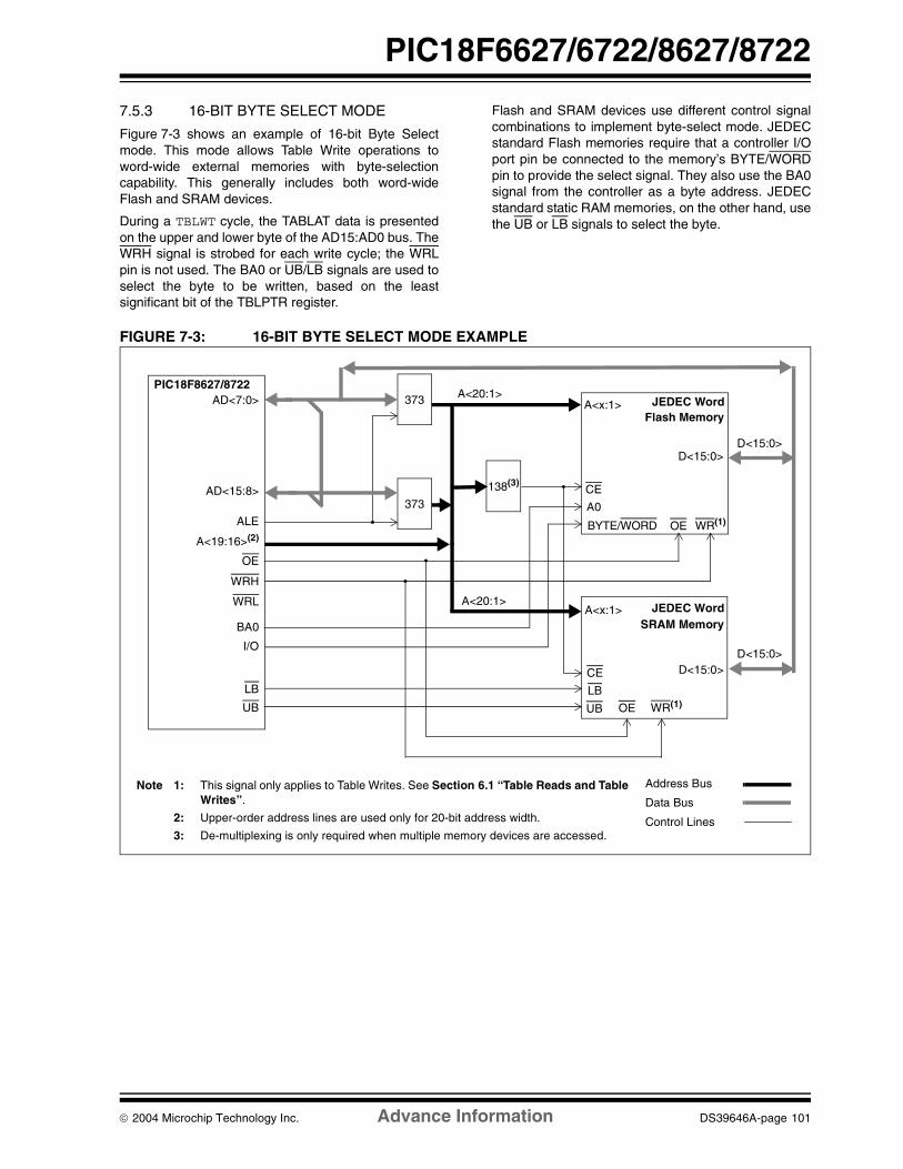
2004 Microchip Technology Inc. Advance Information DS39646A-page 101
PIC18F6627/6722/8627/8722
7.5.3 16-BIT BYTE SELECT MODE
Figure 7-3 shows an example of 16-bit Byte Selectmode. This mode allows Table Write operations toword-wide external memories with byte-selectioncapability. This generally includes both word-wideFlash and SRAM devices.
During a TBLWT cycle, the TABLAT data is presentedon the upper and lower byte of the AD15:AD0 bus. TheWRH signal is strobed for each write cycle; the WRLpin is not used. The BA0 or UB/LB signals are used toselect the byte to be written, based on the leastsignificant bit of the TBLPTR register.
Flash and SRAM devices use different control signalcombinations to implement byte-select mode. JEDECstandard Flash memories require that a controller I/Oport pin be connected to the memory’s BYTE/WORDpin to provide the select signal. They also use the BA0signal from the controller as a byte address. JEDECstandard static RAM memories, on the other hand, usethe UB or LB signals to select the byte.
FIGURE 7-3: 16-BIT BYTE SELECT MODE EXAMPLE
AD<7:0>PIC18F8627/8722
AD<15:8>
ALE
373 A<20:1>
373
OE
WRH
A<19:16>(2)
WRL
BA0
JEDEC WordA<x:1>
D<15:0>
A<20:1>
CE
D<15:0>
I/O
OE WR(1)
A0
BYTE/WORD
Flash Memory
JEDEC WordA<x:1>
D<15:0>CE
D<15:0>
OE WR(1)
LB
UB
SRAM Memory
LB
UB
138(3)
Address Bus
Data Bus
Control Lines
Note 1: This signal only applies to Table Writes. See Section 6.1 “Table Reads and Table Writes”.
2: Upper-order address lines are used only for 20-bit address width.
3: De-multiplexing is only required when multiple memory devices are accessed.

PIC18F6627/6722/8627/8722
DS39646A-page 102 Advance Information 2004 Microchip Technology Inc.
7.5.4 16-BIT MODE TIMING
The presentation of control signals on the externalmemory bus is different for the various operatingmodes. Typical signal timing diagrams are shown inFigure 7-4 through Figure 7-6. All examples assumeeither 20-bit or 21-bit address widths.
FIGURE 7-4: EXTERNAL MEMORY BUS TIMING FOR TBLRD WITH A 1 TCY WAIT STATE (MICROPROCESSOR MODE)
FIGURE 7-5: EXTERNAL MEMORY BUS TIMING FOR TBLRD (EXTENDED MICROCONTROLLER MODE)
Q2Q1 Q3 Q4 Q2Q1 Q3 Q4 Q4Q4 Q4 Q4
ALE
OE
3AABh
WRH
WRL
AD<15:0>
BA0
CF33h
Opcode FetchMOVLW 55h
from 007556h
9256h0E55h
‘1’ ‘1’
‘1’‘1’
Table Readof 92h
from 199E67h
1TCY Wait
Q2Q1 Q3 Q4 Q2Q1 Q3 Q4 Q2Q1 Q3 Q4Apparent Q
Actual Q
A<19:16> 0Ch00h
CE ‘0’‘0’
MemoryCycle
InstructionExecution TBLRD Cycle1 TBLRD Cycle2
Q2Q1 Q3 Q4 Q2Q1 Q3 Q4 Q2Q1 Q3 Q4
A<19:16>
ALE
OE
AD<15:0>
CE
Opcode Fetch Opcode Fetch Opcode FetchTBLRD *
TBLRD Cycle1
ADDLW 55hfrom 000100h
Q2Q1 Q3 Q4
0Ch
CF33h
TBLRD 92hfrom 199E67h
9256h
from 000104h
MemoryCycle
InstructionExecution INST(PC-2) TBLRD Cycle2
MOVLW 55hfrom 000102h
MOVLW

2004 Microchip Technology Inc. Advance Information DS39646A-page 103
PIC18F6627/6722/8627/8722
FIGURE 7-6: EXTERNAL BUS TIMING FOR SLEEP (MICROPROCESSOR MODE)
Q2Q1 Q3 Q4 Q2Q1 Q3 Q4
A<19:16>
ALE
OE
3AAAhAD<15:0>
00h 00h
CE
Opcode Fetch Opcode FetchSLEEP
SLEEP
from 007554h
Q1
Bus Inactive(1)
0003h 3AABh 0E55h
MemoryCycle
InstructionExecution INST(PC-2)
Sleep Mode, MOVLW 55h
from 007556h
Note 1: Bus becomes inactive regardless of power-managed mode entered when SLEEP is executed.
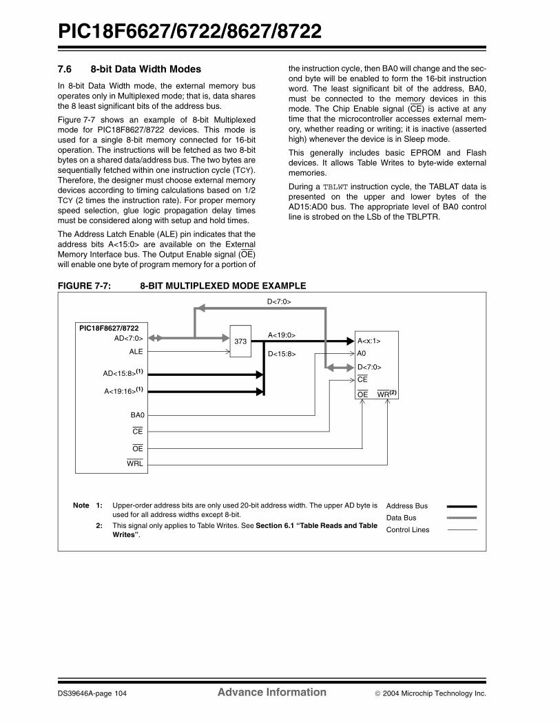
PIC18F6627/6722/8627/8722
DS39646A-page 104 Advance Information 2004 Microchip Technology Inc.
7.6 8-bit Data Width Modes
In 8-bit Data Width mode, the external memory busoperates only in Multiplexed mode; that is, data sharesthe 8 least significant bits of the address bus.
Figure 7-7 shows an example of 8-bit Multiplexedmode for PIC18F8627/8722 devices. This mode isused for a single 8-bit memory connected for 16-bitoperation. The instructions will be fetched as two 8-bitbytes on a shared data/address bus. The two bytes aresequentially fetched within one instruction cycle (TCY).Therefore, the designer must choose external memorydevices according to timing calculations based on 1/2TCY (2 times the instruction rate). For proper memoryspeed selection, glue logic propagation delay timesmust be considered along with setup and hold times.
The Address Latch Enable (ALE) pin indicates that theaddress bits A<15:0> are available on the ExternalMemory Interface bus. The Output Enable signal (OE)will enable one byte of program memory for a portion of
the instruction cycle, then BA0 will change and the sec-ond byte will be enabled to form the 16-bit instructionword. The least significant bit of the address, BA0,must be connected to the memory devices in thismode. The Chip Enable signal (CE) is active at anytime that the microcontroller accesses external mem-ory, whether reading or writing; it is inactive (assertedhigh) whenever the device is in Sleep mode.
This generally includes basic EPROM and Flashdevices. It allows Table Writes to byte-wide externalmemories.
During a TBLWT instruction cycle, the TABLAT data ispresented on the upper and lower bytes of theAD15:AD0 bus. The appropriate level of BA0 controlline is strobed on the LSb of the TBLPTR.
FIGURE 7-7: 8-BIT MULTIPLEXED MODE EXAMPLE
AD<7:0>
A<19:16>(1)
ALE D<15:8>
373A<19:0>
A<x:1>
D<7:0>
OE
OE WR(2)
CE
Note 1: Upper-order address bits are only used 20-bit address width. The upper AD byte is used for all address widths except 8-bit.
2: This signal only applies to Table Writes. See Section 6.1 “Table Reads and Table Writes”.
WRL
D<7:0>
PIC18F8627/8722
AD<15:8>(1)
Address Bus
Data Bus
Control Lines
CE
A0
BA0

2004 Microchip Technology Inc. Advance Information DS39646A-page 105
PIC18F6627/6722/8627/8722
7.6.1 8-BIT MODE TIMING
The presentation of control signals on the externalmemory bus is different for the various operatingmodes. Typical signal timing diagrams are shown inFigure 7-8 through Figure 7-11.
FIGURE 7-8: EXTERNAL BUS TIMING FOR TBLRD (MICROPROCESSOR MODE)
FIGURE 7-9: EXTERNAL BUS TIMING FOR TBLRD (EXTENDED MICROCONTROLLER MODE)
Q2Q1 Q3 Q4 Q2Q1 Q3 Q4 Q2Q1 Q3 Q4
AD<15:8>,
ALE
OE
AAh
WRH
WRL
AD<7:0>
03Ah 03Ah
BA0
Opcode Fetch Opcode Fetch Opcode Fetch
TBLRD *
TBLRD Cycle1
ADDLW 55hfrom 007554h
08h
‘1’
Q2Q1 Q3 Q4
CCFh
33h
Table Read 92h
from 199E67h
92h
‘1’
00h ABh 55h 0Eh ACh 55h 0Fh
03Ah
‘1’ ‘1’
from 007558h
MemoryCycle
InstructionExecution INST(PC-2) TBLRD Cycle2
MOVLW 55hfrom 007556h
MOVLW
A<19:16>(1)
Note 1: The address lines actually used depends on the address width selected. This example assumes 20-bit addressing.
Q2Q1 Q3 Q4 Q2Q1 Q3 Q4 Q2Q1 Q3 Q4
A<19:16>(1)
ALE
OE
AD<7:0>
CE
Opcode Fetch Opcode Fetch Opcode FetchTBLRD *
TBLRD Cycle1
ADDLW 55hfrom 000100h
Q2Q1 Q3 Q4
0Ch
33h
TBLRD 92hfrom 199E67h
92h
from 000104h
MemoryCycle
InstructionExecution INST(PC-2) TBLRD Cycle2
MOVLW 55hfrom 000102h
MOVLW
AD<15:8>(1) CFh
Note 1: The address lines actually used depends on the address width selected. This example assumes 20-bit addressing.

PIC18F6627/6722/8627/8722
DS39646A-page 106 Advance Information 2004 Microchip Technology Inc.
FIGURE 7-10: EXTERNAL MEMORY BUS TIMING FOR SLEEP (MICROPROCESSOR MODE)
FIGURE 7-11: TYPICAL OPCODE FETCH, 8-BIT MODE
Q2Q1 Q3 Q4 Q2Q1 Q3 Q4
A<19:16>(1)
ALE
OE
AAhAD<7:0>
00h 00h
CE
Opcode Fetch Opcode FetchSLEEP
SLEEP
from 007554h
Q1
Bus Inactive(2)
00h ABh 55h
MemoryCycle
InstructionExecution INST(PC-2)
Sleep Mode, MOVLW 55h
from 007556h
AD<15:8>(1) 3Ah 3Ah
03h 0Eh
BA0
Note 1: The address lines actually used depends on the address width selected. This example assumes 20-bit addressing.
2: Bus becomes inactive regardless of power-managed mode entered when SLEEP is executed.
Q2Q1 Q3 Q4
AD<15:8>,
ALE
OE
WRL
AD<7:0>
03Ah
BA0
Opcode Fetch
55h0Eh
‘1’ ‘1’
MemoryCycle
MOVLW 55h from 007556h
55h
A16(1)
Note 1: The address lines actually used depends on the address width selected. This example assumes 16-bit addressing.

2004 Microchip Technology Inc. Advance Information DS39646A-page 107
PIC18F6627/6722/8627/8722
7.7 Operation in Power-Managed Modes
In alternate power-managed Run modes, the externalbus continues to operate normally. If a clock sourcewith a lower speed is selected, bus operations will runat that speed. In these cases, excessive access timesfor the external memory may result if wait states havebeen enabled and added to external memory opera-tions. If operations in a lower power Run mode areanticipated, users should provide in their applicationsfor adjusting memory access times at the lower clockspeeds.
In Sleep and Idle modes, the microcontroller core doesnot need to access data; bus operations are sus-pended. The state of the external bus is frozen, with theaddress/data pins and most of the control pins holdingat the same state they were in when the mode wasinvoked. The only potential changes are the CE, LBand UB pins, which are held at logic high.
TABLE 7-3: SUMMARY OF REGISTERS ASSOCIATED WITH POWER-MANAGED MODES
Name Bit 7 Bit 6 Bit 5 Bit 4 Bit 3 Bit 2 Bit 1 Bit 0Reset Values
on Page
MEMCON(1) EBDIS — WAIT1 WAIT0 — — WM1 WM0 60
CONFIG3L(2) WAIT BW ABW1 ABW0 — — PM1 PM0 299
CONFIG3H MCLRE — — — — LPT1OSC ECCPMX CCP2MX 300
Legend: — = unimplemented, read as ‘0’. Shaded cells are not used by the External Memory Bus.Note 1: This register is not implemented on 64-pin devices.
2: Unimplemented in PIC18F6627/6722 devices.

PIC18F6627/6722/8627/8722
DS39646A-page 108 Advance Information 2004 Microchip Technology Inc.
NOTES:
2004 Microchip Technology Inc. Advance Information DS39646A-page 109
PIC18F6627/6722/8627/8722
8.0 DATA EEPROM MEMORY
The data EEPROM is a nonvolatile memory array, sep-arate from the data RAM and program memory, that isused for long-term storage of program data. It is notdirectly mapped in either the register file or programmemory space, but is indirectly addressed through theSpecial Function Registers (SFRs). The EEPROM isreadable and writable during normal operation over theentire VDD range.
Five SFRs are used to read and write to the dataEEPROM, as well as the program memory. They are:
• EECON1• EECON2
• EEDATA• EEADR• EEADRH
The data EEPROM allows byte read and write. Wheninterfacing to the data memory block, EEDATA holdsthe 8-bit data for read/write and the EEADRH:EEADRregister pair holds the address of the EEPROM locationbeing accessed.
The EEPROM data memory is rated for high erase/writecycle endurance. A byte write automatically erases thelocation and writes the new data (erase-before-write).The write time is controlled by an on-chip timer; it willvary with voltage and temperature, as well as from chip-to-chip. Please refer to parameter D122 (Table 28-1 inSection 28.0 “Electrical Characteristics”) for exactlimits.
8.1 EEADR and EEADRH Registers
The EEADRH:EEADR register pair is used to addressthe data EEPROM for read and write operations.EEADRH holds the two MSbits of the address; theupper 6 bits are ignored. The 10-bit range of the paircan address a memory range of 1024 bytes (00h to3FFh).
8.2 EECON1 and EECON2 Registers
Access to the data EEPROM is controlled by tworegisters: EECON1 and EECON2. These are the sameregisters which control access to the program memoryand are used in a similar manner for the dataEEPROM.
The EECON1 register (Register 8-1) is the controlregister for data and program memory access. Controlbit EEPGD determines if the access will be to programor data EEPROM memory. When clear, operations willaccess the data EEPROM memory. When set, programmemory is accessed.
Control bit CFGS determines if the access will be to theconfiguration registers or to program memory/dataEEPROM memory. When set, subsequent operationsaccess configuration registers. When CFGS is clear,the EEPGD bit selects either program Flash or dataEEPROM memory.
The WREN bit, when set, will allow a write operation.On power-up, the WREN bit is clear. The WRERR bit isset in hardware when the WREN bit is set and clearedwhen the internal programming timer expires and thewrite operation is complete.
The WR control bit initiates write operations. The bitcannot be cleared, only set, in software; it is cleared inhardware at the completion of the write operation.
Control bits, RD and WR, start read and erase/writeoperations, respectively. These bits are set by firmwareand cleared by hardware at the completion of theoperation.
The RD bit cannot be set when accessing programmemory (EEPGD = 1). Program memory is read usingTable Read instructions. See Section 6.1 “TableReads and Table Writes” regarding Table Reads.
The EECON2 register is not a physical register. It isused exclusively in the memory write and erasesequences. Reading EECON2 will read all ‘0’s.
Note: During normal operation, the WRERR isread as ‘1’. This can indicate that a writeoperation was prematurely terminated bya Reset, or a write operation wasattempted improperly.
Note: The EEIF interrupt flag bit (PIR2<4>) is setwhen the write is complete. It must becleared in software.

PIC18F6627/6722/8627/8722
DS39646A-page 110 Advance Information 2004 Microchip Technology Inc.
REGISTER 8-1: EECON1: DATA EEPROM CONTROL REGISTER 1 R/W-x R/W-x U-0 R/W-0 R/W-x R/W-0 R/S-0 R/S-0
EEPGD CFGS — FREE WRERR WREN WR RD
bit 7 bit 0
bit 7 EEPGD: Flash Program or Data EEPROM Memory Select bit1 = Access Flash program memory0 = Access data EEPROM memory
bit 6 CFGS: Flash Program/Data EEPROM or Configuration Select bit
1 = Access configuration registers0 = Access Flash program or data EEPROM memory
bit 5 Unimplemented: Read as ‘0’
bit 4 FREE: Flash Row Erase Enable bit1 = Erase the program memory row addressed by TBLPTR on the next WR command (cleared
by completion of erase operation)0 = Perform write only
bit 3 WRERR: Flash Program/Data EEPROM Error Flag bit1 = A write operation is prematurely terminated (any Reset during self-timed programming in
normal operation, or an improper write attempt)0 = The write operation completed
Note: When a WRERR occurs, the EEPGD and CFGS bits are not cleared. This allows tracing of the error condition.
bit 2 WREN: Flash Program/Data EEPROM Write Enable bit1 = Allows write cycles to Flash program/data EEPROM0 = Inhibits write cycles to Flash program/data EEPROM
bit 1 WR: Write Control bit1 = Initiates a data EEPROM erase/write cycle or a program memory erase cycle or write cycle.
(The operation is self-timed and the bit is cleared by hardware once write is complete. The WR bit can only be set (not cleared) in software.)
0 = Write cycle to the EEPROM is complete
bit 0 RD: Read Control bit1 = Initiates an EEPROM read
(Read takes one cycle. RD is cleared in hardware. The RD bit can only be set (not cleared)in software. RD bit cannot be set when EEPGD = 1 or CFGS = 1.)
0 = Does not initiate an EEPROM read
Legend:
R = Readable bit W = Writable bit U = Unimplemented bit, read as ‘0’
-n = Value at POR ‘1’ = Bit is set ‘0’ = Bit is cleared x = Bit is unknown

2004 Microchip Technology Inc. Advance Information DS39646A-page 111
PIC18F6627/6722/8627/8722
8.3 Reading the Data EEPROM Memory
To read a data memory location, the user must write theaddress to the EEADRH:EEADR register pair, clear theEEPGD control bit (EECON1<7>) and then set controlbit, RD (EECON1<0>). The data is available on thevery next instruction cycle; therefore, the EEDATAregister can be read by the next instruction. EEDATAwill hold this value until another read operation, or untilit is written to by the user (during a write operation).
The basic process is shown in Example 8-1.
8.4 Writing to the Data EEPROM Memory
To write an EEPROM data location, the address mustfirst be written to the EEADRH:EEADR register pairand the data written to the EEDATA register. Thesequence in Example 8-2 must be followed to initiatethe write cycle.
The write will not begin if this sequence is not exactlyfollowed (write 55h to EECON2, write 0AAh toEECON2, then set WR bit) for each byte. It is stronglyrecommended that interrupts be disabled during thiscode segment.
Additionally, the WREN bit in EECON1 must be set toenable writes. This mechanism prevents accidentalwrites to data EEPROM due to unexpected code exe-cution (i.e., runaway programs). The WREN bit shouldbe kept clear at all times, except when updating theEEPROM. The WREN bit is not cleared by hardware.
After a write sequence has been initiated, EECON1,EEADRH:EEADR and EEDATA cannot be modified.The WR bit will be inhibited from being set unless theWREN bit is set. The WREN bit must be set on a pre-vious instruction. Both WR and WREN cannot be setwith the same instruction.
At the completion of the write cycle, the WR bit iscleared in hardware and the EEPROM Interrupt Flag bit(EEIF) is set. The user may either enable this interrupt,or poll this bit. EEIF must be cleared by software.
8.5 Write Verify
Depending on the application, good programmingpractice may dictate that the value written to the mem-ory should be verified against the original value. Thisshould be used in applications where excessive writescan stress bits near the specification limit.
EXAMPLE 8-1: DATA EEPROM READ
EXAMPLE 8-2: DATA EEPROM WRITE
MOVLW DATA_EE_ADDRH ;MOVWF EEADRH ; Upper bits of Data Memory Address to readMOVLW DATA_EE_ADDR ;MOVWF EEADR ; Lower bits of Data Memory Address to readBCF EECON1, EEPGD ; Point to DATA memoryBCF EECON1, CFGS ; Access EEPROMBSF EECON1, RD ; EEPROM ReadMOVF EEDATA, W ; W = EEDATA
MOVLW DATA_EE_ADDRH ;MOVWF EEADRH ; Upper bits of Data Memory Address to writeMOVLW DATA_EE_ADDR ;MOVWF EEADR ; Lower bits of Data Memory Address to writeMOVLW DATA_EE_DATA ;MOVWF EEDATA ; Data Memory Value to writeBCF EECON1, EPGD ; Point to DATA memoryBCF EECON1, CFGS ; Access EEPROMBSF EECON1, WREN ; Enable writes
BCF INTCON, GIE ; Disable InterruptsMOVLW 55h ;
Required MOVWF EECON2 ; Write 55hSequence MOVLW 0AAh ;
MOVWF EECON2 ; Write 0AAhBSF EECON1, WR ; Set WR bit to begin writeBSF INTCON, GIE ; Enable Interrupts
; User code executionBCF EECON1, WREN ; Disable writes on write complete (EEIF set)

PIC18F6627/6722/8627/8722
DS39646A-page 112 Advance Information 2004 Microchip Technology Inc.
8.6 Operation During Code-Protect
Data EEPROM memory has its own code-protect bits inconfiguration words. External read and writeoperations are disabled if code protection is enabled.
The microcontroller itself can both read and write to theinternal data EEPROM, regardless of the state of thecode-protect configuration bit. Refer to Section 25.0“Special Features of the CPU” for additionalinformation.
8.7 Protection Against Spurious Write
There are conditions when the device may not want towrite to the data EEPROM memory. To protect againstspurious EEPROM writes, various mechanisms havebeen implemented. On power-up, the WREN bit iscleared. In addition, writes to the EEPROM are blockedduring the Power-up Timer period (TPWRT,parameter 33).
The write initiate sequence and the WREN bit togetherhelp prevent an accidental write during brown-out,power glitch or software malfunction.
8.8 Using the Data EEPROM
The data EEPROM is a high endurance, byte address-able array that has been optimized for the storage offrequently changing information (e.g., programvariables or other data that are updated often).Frequently changing values will typically be updatedmore often than specification D124. If this is not thecase, an array refresh must be performed. For thisreason, variables that change infrequently (such asconstants, IDs, calibration, etc.) should be stored inFlash program memory.
A simple data EEPROM refresh routine is shown inExample 8-3.
EXAMPLE 8-3: DATA EEPROM REFRESH ROUTINE
Note: If data EEPROM is only used to storeconstants and/or data that changes often,an array refresh is likely not required. Seespecification D124.
CLRF EEADR ; Start at address 0CLRF EEADRH ;BCF EECON1, CFGS ; Set for memoryBCF EECON1, EEPGD ; Set for Data EEPROMBCF INTCON, GIE ; Disable interruptsBSF EECON1, WREN ; Enable writes
Loop ; Loop to refresh arrayBSF EECON1, RD ; Read current addressMOVLW 55h ;MOVWF EECON2 ; Write 55hMOVLW 0AAh ;MOVWF EECON2 ; Write 0AAhBSF EECON1, WR ; Set WR bit to begin writeBTFSC EECON1, WR ; Wait for write to completeBRA $-2INCFSZ EEADR, F ; Increment addressBRA LOOP ; Not zero, do it againINCFSZ EEADRH, F ; Increment the high addressBRA LOOP ; Not zero, do it again
BCF EECON1, WREN ; Disable writesBSF INTCON, GIE ; Enable interrupts

2004 Microchip Technology Inc. Advance Information DS39646A-page 113
PIC18F6627/6722/8627/8722
TABLE 8-1: REGISTERS ASSOCIATED WITH DATA EEPROM MEMORY
Name Bit 7 Bit 6 Bit 5 Bit 4 Bit 3 Bit 2 Bit 1 Bit 0Reset Values
on page
INTCON GIE/GIEH PEIE/GIEL TMR0IE INT0IE RBIE TMR0IF INT0IF RBIF 57
EEADRH — — — — — — EEPROM Address Register High Byte
59
EEADR EEPROM Address Register 59
EEDATA EEPROM Data Register 59
EECON2 EEPROM Control Register 2 (not a physical register) 59
EECON1 EEPGD CFGS — FREE WRERR WREN WR RD 59
IPR2 OSCFIP CMIP(1) — EEIP BCL1IP HLVDIP TMR3IP CCP2IP(1) 60
PIR2 OSCFIF CMIF(1) — EEIF BCL1IF HLVDIF TMR3IF CCP2IF(1) 60
PIE2 OSCFIE CMIE(1) — EEIE BCL1IE HLVDIE TMR3IE CCP2IE(1) 60
Legend: — = unimplemented, read as ‘0’. Shaded cells are not used during Flash/EEPROM access.Note 1: These bits are available in 80-pin devices and reserved in 64-pin devices.

PIC18F6627/6722/8627/8722
DS39646A-page 114 Advance Information 2004 Microchip Technology Inc.
NOTES:
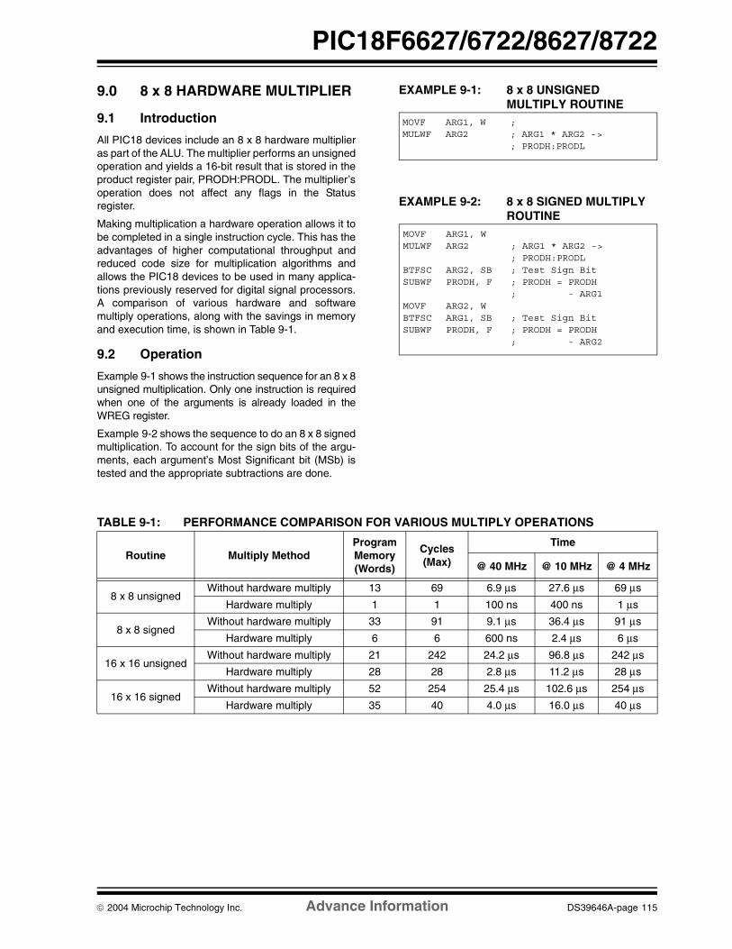
2004 Microchip Technology Inc. Advance Information DS39646A-page 115
PIC18F6627/6722/8627/8722
9.0 8 x 8 HARDWARE MULTIPLIER
9.1 Introduction
All PIC18 devices include an 8 x 8 hardware multiplieras part of the ALU. The multiplier performs an unsignedoperation and yields a 16-bit result that is stored in theproduct register pair, PRODH:PRODL. The multiplier’soperation does not affect any flags in the Statusregister.
Making multiplication a hardware operation allows it tobe completed in a single instruction cycle. This has theadvantages of higher computational throughput andreduced code size for multiplication algorithms andallows the PIC18 devices to be used in many applica-tions previously reserved for digital signal processors.A comparison of various hardware and softwaremultiply operations, along with the savings in memoryand execution time, is shown in Table 9-1.
9.2 Operation
Example 9-1 shows the instruction sequence for an 8 x 8unsigned multiplication. Only one instruction is requiredwhen one of the arguments is already loaded in theWREG register.
Example 9-2 shows the sequence to do an 8 x 8 signedmultiplication. To account for the sign bits of the argu-ments, each argument’s Most Significant bit (MSb) istested and the appropriate subtractions are done.
EXAMPLE 9-1: 8 x 8 UNSIGNED MULTIPLY ROUTINE
EXAMPLE 9-2: 8 x 8 SIGNED MULTIPLY ROUTINE
TABLE 9-1: PERFORMANCE COMPARISON FOR VARIOUS MULTIPLY OPERATIONS
MOVF ARG1, W ; MULWF ARG2 ; ARG1 * ARG2 ->
; PRODH:PRODL
MOVF ARG1, W MULWF ARG2 ; ARG1 * ARG2 ->
; PRODH:PRODL BTFSC ARG2, SB ; Test Sign Bit SUBWF PRODH, F ; PRODH = PRODH
; - ARG1 MOVF ARG2, WBTFSC ARG1, SB ; Test Sign Bit SUBWF PRODH, F ; PRODH = PRODH
; - ARG2
Routine Multiply MethodProgramMemory(Words)
Cycles(Max)
Time
@ 40 MHz @ 10 MHz @ 4 MHz
8 x 8 unsignedWithout hardware multiply 13 69 6.9 µs 27.6 µs 69 µs
Hardware multiply 1 1 100 ns 400 ns 1 µs
8 x 8 signedWithout hardware multiply 33 91 9.1 µs 36.4 µs 91 µs
Hardware multiply 6 6 600 ns 2.4 µs 6 µs
16 x 16 unsignedWithout hardware multiply 21 242 24.2 µs 96.8 µs 242 µs
Hardware multiply 28 28 2.8 µs 11.2 µs 28 µs
16 x 16 signedWithout hardware multiply 52 254 25.4 µs 102.6 µs 254 µs
Hardware multiply 35 40 4.0 µs 16.0 µs 40 µs

PIC18F6627/6722/8627/8722
DS39646A-page 116 Advance Information 2004 Microchip Technology Inc.
Example 9-3 shows the sequence to do a 16 x 16unsigned multiplication. Equation 9-1 shows thealgorithm that is used. The 32-bit result is stored in fourregisters (RES3:RES0).
EQUATION 9-1: 16 x 16 UNSIGNED MULTIPLICATION ALGORITHM
EXAMPLE 9-3: 16 x 16 UNSIGNED MULTIPLY ROUTINE
Example 9-4 shows the sequence to do a 16 x 16signed multiply. Equation 9-2 shows the algorithmused. The 32-bit result is stored in four registers(RES3:RES0). To account for the sign bits of the argu-ments, the MSb for each argument pair is tested andthe appropriate subtractions are done.
EQUATION 9-2: 16 x 16 SIGNED MULTIPLICATION ALGORITHM
EXAMPLE 9-4: 16 x 16 SIGNED MULTIPLY ROUTINE
RES3:RES0 = ARG1H:ARG1L • ARG2H:ARG2L= (ARG1H • ARG2H • 216) +
(ARG1H • ARG2L • 28) +(ARG1L • ARG2H • 28) +(ARG1L • ARG2L)
MOVF ARG1L, W MULWF ARG2L ; ARG1L * ARG2L->
; PRODH:PRODL MOVFF PRODH, RES1 ; MOVFF PRODL, RES0 ;
; MOVF ARG1H, W MULWF ARG2H ; ARG1H * ARG2H->
; PRODH:PRODL MOVFF PRODH, RES3 ; MOVFF PRODL, RES2 ;
; MOVF ARG1L, W MULWF ARG2H ; ARG1L * ARG2H->
; PRODH:PRODL MOVF PRODL, W ; ADDWF RES1, F ; Add cross MOVF PRODH, W ; products ADDWFC RES2, F ; CLRF WREG ; ADDWFC RES3, F ;
; MOVF ARG1H, W ; MULWF ARG2L ; ARG1H * ARG2L->
; PRODH:PRODL MOVF PRODL, W ; ADDWF RES1, F ; Add cross MOVF PRODH, W ; products ADDWFC RES2, F ; CLRF WREG ; ADDWFC RES3, F ;
RES3:RES0 = ARG1H:ARG1L • ARG2H:ARG2L= (ARG1H • ARG2H • 216) +
(ARG1H • ARG2L • 28) +(ARG1L • ARG2H • 28) +(ARG1L • ARG2L) +(-1 • ARG2H<7> • ARG1H:ARG1L • 216) +(-1 • ARG1H<7> • ARG2H:ARG2L • 216)
MOVF ARG1L, W MULWF ARG2L ; ARG1L * ARG2L ->
; PRODH:PRODL MOVFF PRODH, RES1 ; MOVFF PRODL, RES0 ;
; MOVF ARG1H, W MULWF ARG2H ; ARG1H * ARG2H ->
; PRODH:PRODL MOVFF PRODH, RES3 ; MOVFF PRODL, RES2 ;
; MOVF ARG1L, W MULWF ARG2H ; ARG1L * ARG2H ->
; PRODH:PRODL MOVF PRODL, W ; ADDWF RES1, F ; Add cross MOVF PRODH, W ; products ADDWFC RES2, F ; CLRF WREG ; ADDWFC RES3, F ;
; MOVF ARG1H, W ; MULWF ARG2L ; ARG1H * ARG2L ->
; PRODH:PRODL MOVF PRODL, W ; ADDWF RES1, F ; Add cross MOVF PRODH, W ; products ADDWFC RES2, F ; CLRF WREG ; ADDWFC RES3, F ;
; BTFSS ARG2H, 7 ; ARG2H:ARG2L neg? BRA SIGN_ARG1 ; no, check ARG1 MOVF ARG1L, W ; SUBWF RES2 ; MOVF ARG1H, W ; SUBWFB RES3
; SIGN_ARG1
BTFSS ARG1H, 7 ; ARG1H:ARG1L neg? BRA CONT_CODE ; no, done MOVF ARG2L, W ; SUBWF RES2 ; MOVF ARG2H, W ; SUBWFB RES3
; CONT_CODE :
2004 Microchip Technology Inc. Advance Information DS39646A-page 117
PIC18F6627/6722/8627/8722
10.0 INTERRUPTS
The PIC18F6627/6722/8627/8722 devices havemultiple interrupt sources and an interrupt priority fea-ture that allows most interrupt sources to be assigneda high priority level or a low priority level. The highpriority interrupt vector is at 0008h and the low priorityinterrupt vector is at 0018h. High priority interruptevents will interrupt any low priority interrupts that maybe in progress.
There are ten registers which are used to controlinterrupt operation. These registers are:
• RCON• INTCON
• INTCON2• INTCON3• PIR1, PIR2, PIR3
• PIE1, PIE2, PIE3• IPR1, IPR2, IPR3
It is recommended that the Microchip header files sup-plied with MPLAB® IDE be used for the symbolic bitnames in these registers. This allows the assembler/compiler to automatically take care of the placement ofthese bits within the specified register.
In general, interrupt sources have three bits to controltheir operation. They are:
• Flag bit to indicate that an interrupt event occurred
• Enable bit that allows program execution to branch to the interrupt vector address when the flag bit is set
• Priority bit to select high priority or low priority
The interrupt priority feature is enabled by setting theIPEN bit (RCON<7>). When interrupt priority isenabled, there are two bits which enable interruptsglobally. Setting the GIEH bit (INTCON<7>) enables allinterrupts that have the priority bit set (high priority).Setting the GIEL bit (INTCON<6>) enables allinterrupts that have the priority bit cleared (low priority).When the interrupt flag, enable bit and appropriateglobal interrupt enable bit are set, the interrupt willvector immediately to address 0008h or 0018h,depending on the priority bit setting. Individualinterrupts can be disabled through their correspondingenable bits.
When the IPEN bit is cleared (default state), theinterrupt priority feature is disabled and interrupts arecompatible with PICmicro® mid-range devices. InCompatibility mode, the interrupt priority bits for eachsource have no effect. INTCON<6> is the PEIE bit,which enables/disables all peripheral interrupt sources.INTCON<7> is the GIE bit, which enables/disables allinterrupt sources. All interrupts branch to address0008h in Compatibility mode.
When an interrupt is responded to, the global interruptenable bit is cleared to disable further interrupts. If theIPEN bit is cleared, this is the GIE bit. If interrupt prioritylevels are used, this will be either the GIEH or GIEL bit.High priority interrupt sources can interrupt a lowpriority interrupt. Low priority interrupts are notprocessed while high priority interrupts are in progress.
The return address is pushed onto the stack and thePC is loaded with the interrupt vector address (0008hor 0018h). Once in the Interrupt Service Routine, thesource(s) of the interrupt can be determined by pollingthe interrupt flag bits. The interrupt flag bits must becleared in software before re-enabling interrupts toavoid recursive interrupts.
The “return from interrupt” instruction, RETFIE, exitsthe interrupt routine and sets the GIE bit (GIEH or GIELif priority levels are used), which re-enables interrupts.
For external interrupt events, such as the INT pins orthe PORTB input change interrupt, the interrupt latencywill be three to four instruction cycles. The exactlatency is the same for one or two-cycle instructions.Individual interrupt flag bits are set, regardless of thestatus of their corresponding enable bit or the GIE bit.
Note: Do not use the MOVFF instruction to modifyany of the interrupt control registers whileany interrupt is enabled. Doing so maycause erratic microcontroller behavior.
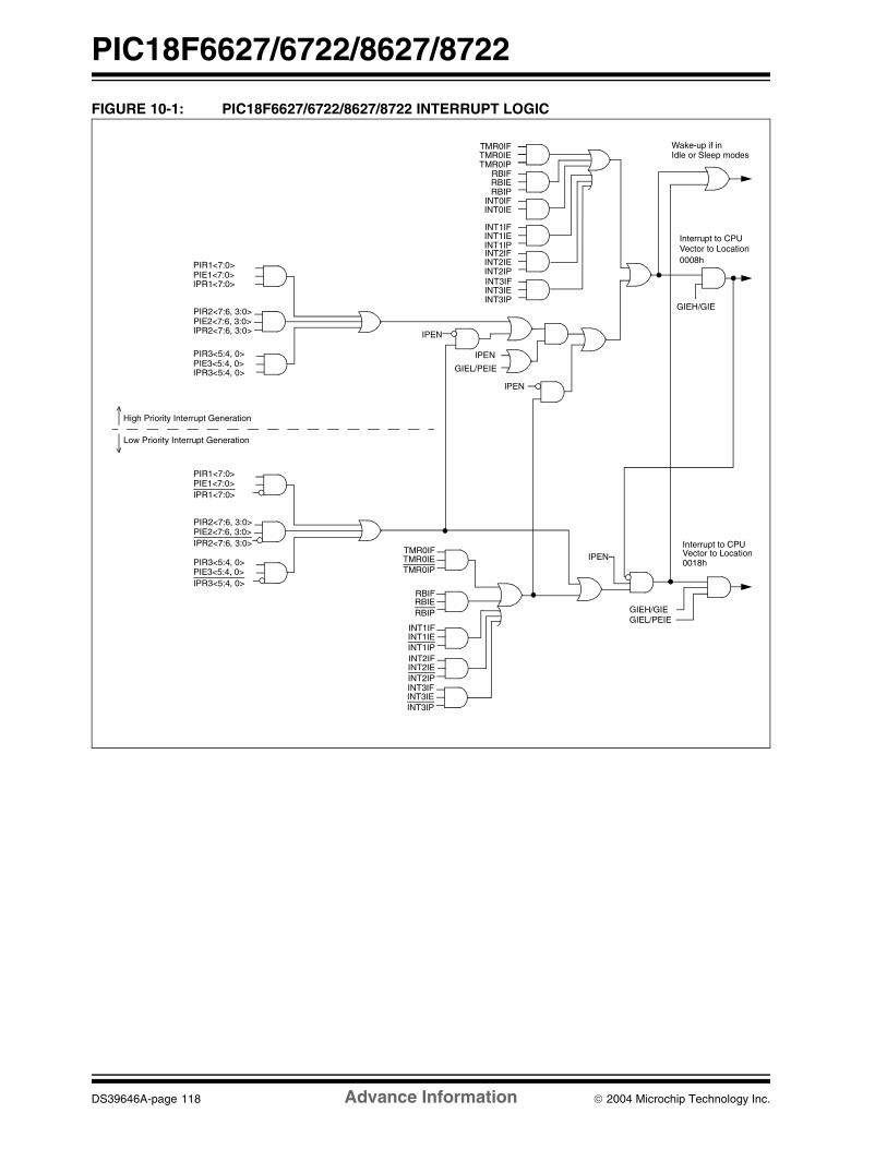
PIC18F6627/6722/8627/8722
DS39646A-page 118 Advance Information 2004 Microchip Technology Inc.
FIGURE 10-1: PIC18F6627/6722/8627/8722 INTERRUPT LOGIC
TMR0IE
GIEH/GIE
GIEL/PEIE
Wake-up if in
Interrupt to CPUVector to Location0008h
INT2IFINT2IEINT2IP
INT1IFINT1IEINT1IP
TMR0IFTMR0IETMR0IP
RBIFRBIERBIP
IPEN
TMR0IF
TMR0IP
INT1IFINT1IEINT1IPINT2IFINT2IEINT2IP
RBIFRBIERBIP
INT0IFINT0IE
GIEL/PEIE
Interrupt to CPUVector to Location
IPEN
IPEN
0018h
PIR1<7:0>PIE1<7:0> IPR1<7:0>
High Priority Interrupt Generation
Low Priority Interrupt Generation
Idle or Sleep modes
GIEH/GIE
INT3IFINT3IEINT3IP
INT3IFINT3IEINT3IP
PIR2<7:6, 3:0>PIE2<7:6, 3:0> IPR2<7:6, 3:0>
PIR3<5:4, 0>PIE3<5:4, 0> IPR3<5:4, 0>
PIR1<7:0>PIE1<7:0> IPR1<7:0>
PIR2<7:6, 3:0>PIE2<7:6, 3:0> IPR2<7:6, 3:0>
PIR3<5:4, 0>PIE3<5:4, 0> IPR3<5:4, 0>
IPEN

2004 Microchip Technology Inc. Advance Information DS39646A-page 119
PIC18F6627/6722/8627/8722
10.1 INTCON Registers
The INTCON registers are readable and writableregisters which contain various enable, priority and flagbits.
REGISTER 10-1: INTCON: INTERRUPT CONTROL REGISTER
Note: Interrupt flag bits are set when an interruptcondition occurs, regardless of the state ofits corresponding enable bit or the globalinterrupt enable bit. User software shouldensure the appropriate interrupt flag bitsare clear prior to enabling an interrupt.This feature allows for software polling.
R/W-0 R/W-0 R/W-0 R/W-0 R/W-0 R/W-0 R/W-0 R/W-x
GIE/GIEH PEIE/GIEL TMR0IE INT0IE RBIE TMR0IF INT0IF RBIF
bit 7 bit 0
bit 7 GIE/GIEH: Global Interrupt Enable bit
When IPEN = 0:1 = Enables all unmasked interrupts0 = Disables all interrupts When IPEN = 1:1 = Enables all high priority interrupts 0 = Disables all interrupts
bit 6 PEIE/GIEL: Peripheral Interrupt Enable bit
When IPEN = 0:1 = Enables all unmasked peripheral interrupts 0 = Disables all peripheral interrupts When IPEN = 1:1 = Enables all low priority peripheral interrupts 0 = Disables all low priority peripheral interrupts
bit 5 TMR0IE: TMR0 Overflow Interrupt Enable bit
1 = Enables the TMR0 overflow interrupt 0 = Disables the TMR0 overflow interrupt
bit 4 INT0IE: INT0 External Interrupt Enable bit 1 = Enables the INT0 external interrupt 0 = Disables the INT0 external interrupt
bit 3 RBIE: RB Port Change Interrupt Enable bit 1 = Enables the RB port change interrupt 0 = Disables the RB port change interrupt
bit 2 TMR0IF: TMR0 Overflow Interrupt Flag bit
1 = TMR0 register has overflowed (must be cleared in software) 0 = TMR0 register did not overflow
bit 1 INT0IF: INT0 External Interrupt Flag bit 1 = The INT0 external interrupt occurred (must be cleared in software) 0 = The INT0 external interrupt did not occur
bit 0 RBIF: RB Port Change Interrupt Flag bit 1 = At least one of the RB7:RB4 pins changed state (must be cleared in software) 0 = None of the RB7:RB4 pins have changed state
Note: A mismatch condition will continue to set this bit. Reading PORTB will end the mismatch condition and allow the bit to be cleared.
Legend:
R = Readable bit W = Writable bit U = Unimplemented bit, read as ‘0’
-n = Value at POR ‘1’ = Bit is set ‘0’ = Bit is cleared x = Bit is unknown

PIC18F6627/6722/8627/8722
DS39646A-page 120 Advance Information 2004 Microchip Technology Inc.
REGISTER 10-2: INTCON2: INTERRUPT CONTROL REGISTER 2
R/W-1 R/W-1 R/W-1 R/W-1 R/W-1 R/W-1 R/W-1 R/W-1
RBPU INTEDG0 INTEDG1 INTEDG2 INTEDG3 TMR0IP INT3IP RBIP
bit 7 bit 0
bit 7 RBPU: PORTB Pull-up Enable bit 1 = All PORTB pull-ups are disabled 0 = PORTB pull-ups are enabled by individual port latch values
bit 6 INTEDG0: External Interrupt 0 Edge Select bit 1 = Interrupt on rising edge 0 = Interrupt on falling edge
bit 5 INTEDG1: External Interrupt 1 Edge Select bit
1 = Interrupt on rising edge 0 = Interrupt on falling edge
bit 4 INTEDG2: External Interrupt 2 Edge Select bit 1 = Interrupt on rising edge 0 = Interrupt on falling edge
bit 3 INTEDG3: External Interrupt 3 Edge Select bit 1 = Interrupt on rising edge 0 = Interrupt on falling edge
bit 2 TMR0IP: TMR0 Overflow Interrupt Priority bit
1 = High priority 0 = Low priority
bit 1 INT3IP: INT3 External Interrupt Priority bit1 = High priority 0 = Low priority
bit 0 RBIP: RB Port Change Interrupt Priority bit1 = High priority 0 = Low priority
Legend:
R = Readable bit W = Writable bit U = Unimplemented bit, read as ‘0’
-n = Value at POR ‘1’ = Bit is set ‘0’ = Bit is cleared x = Bit is unknown
Note: Interrupt flag bits are set when an interrupt condition occurs, regardless of the stateof its corresponding enable bit or the global interrupt enable bit. User software shouldensure the appropriate interrupt flag bits are clear prior to enabling an interrupt. Thisfeature allows for software polling.

2004 Microchip Technology Inc. Advance Information DS39646A-page 121
PIC18F6627/6722/8627/8722
REGISTER 10-3: INTCON3: INTERRUPT CONTROL REGISTER 3
R/W-1 R/W-1 R/W-0 R/W-0 R/W-0 R/W-0 R/W-0 R/W-0
INT2IP INT1IP INT3IE INT2IE INT1IE INT3IF INT2IF INT1IF
bit 7 bit 0
bit 7 INT2IP: INT2 External Interrupt Priority bit1 = High priority 0 = Low priority
bit 6 INT1IP: INT1 External Interrupt Priority bit
1 = High priority 0 = Low priority
bit 5 INT3IE: INT3 External Interrupt Enable bit1 = Enables the INT3 external interrupt 0 = Disables the INT3 external interrupt
bit 4 INT2IE: INT2 External Interrupt Enable bit1 = Enables the INT2 external interrupt 0 = Disables the INT2 external interrupt
bit 3 INT1IE: INT1 External Interrupt Enable bit
1 = Enables the INT1 external interrupt 0 = Disables the INT1 external interrupt
bit 2 INT3IF: INT3 External Interrupt Flag bit1 = The INT3 external interrupt occurred (must be cleared in software) 0 = The INT3 external interrupt did not occur
bit 1 INT2IF: INT2 External Interrupt Flag bit1 = The INT2 external interrupt occurred (must be cleared in software) 0 = The INT2 external interrupt did not occur
bit 0 INT1IF: INT1 External Interrupt Flag bit
1 = The INT1 external interrupt occurred (must be cleared in software) 0 = The INT1 external interrupt did not occur
Legend:
R = Readable bit W = Writable bit U = Unimplemented bit, read as ‘0’
-n = Value at POR ‘1’ = Bit is set ‘0’ = Bit is cleared x = Bit is unknown
Note: Interrupt flag bits are set when an interrupt condition occurs, regardless of the stateof its corresponding enable bit or the global interrupt enable bit. User softwareshould ensure the appropriate interrupt flag bits are clear prior to enabling aninterrupt. This feature allows for software polling.

PIC18F6627/6722/8627/8722
DS39646A-page 122 Advance Information 2004 Microchip Technology Inc.
10.2 PIR Registers
The PIR registers contain the individual flag bits for theperipheral interrupts. Due to the number of peripheralinterrupt sources, there are three Peripheral InterruptRequest (Flag) registers (PIR1, PIR2, PIR3).
REGISTER 10-4: PIR1: PERIPHERAL INTERRUPT REQUEST (FLAG) REGISTER 1
Note 1: Interrupt flag bits are set when an interruptcondition occurs, regardless of the stateof its corresponding enable bit or theGlobal Interrupt Enable bit, GIE(INTCON<7>).
2: User software should ensure theappropriate interrupt flag bits are clearedprior to enabling an interrupt and afterservicing that interrupt.
R/W-0 R/W-0 R-0 R-0 R/W-0 R/W-0 R/W-0 R/W-0
PSPIF ADIF RC1IF TX1IF SSP1IF CCP1IF TMR2IF TMR1IF
bit 7 bit 0
bit 7 PSPIF: Parallel Slave Port Read/Write Interrupt Flag bit1 = A read or a write operation has taken place (must be cleared in software) 0 = No read or write has occurred
bit 6 ADIF: A/D Converter Interrupt Flag bit 1 = An A/D conversion completed (must be cleared in software) 0 = The A/D conversion is not complete
bit 5 RC1IF: EUSART Receive Interrupt Flag bit
1 = The EUSART receive buffer, RCREGx, is full (cleared when RCREGx is read) 0 = The EUSART receive buffer is empty
bit 4 TX1IF: EUSART Transmit Interrupt Flag bit 1 = The EUSART transmit buffer, TXREGx, is empty (cleared when TXREGx is written) 0 = The EUSART transmit buffer is full
bit 3 SSP1IF: Master Synchronous Serial Port Interrupt Flag bit 1 = The transmission/reception is complete (must be cleared in software)0 = Waiting to transmit/receive
bit 2 CCP1IF: CCP1 Interrupt Flag bit
Capture mode: 1 = A TMR1/TMR3 register capture occurred (must be cleared in software) 0 = No TMR1/TMR3 register capture occurred Compare mode: 1 = A TMR1/TMR3 register compare match occurred (must be cleared in software) 0 = No TMR1/TMR3 register compare match occurredPWM mode: Unused in this mode.
bit 1 TMR2IF: TMR2 to PR2 Match Interrupt Flag bit
1 = TMR2 to PR2 match occurred (must be cleared in software) 0 = No TMR2 to PR2 match occurred
bit 0 TMR1IF: TMR1 Overflow Interrupt Flag bit 1 = TMR1 register overflowed (must be cleared in software)0 = TMR1 register did not overflow
Legend:
R = Readable bit W = Writable bit U = Unimplemented bit, read as ‘0’
-n = Value at POR ‘1’ = Bit is set ‘0’ = Bit is cleared x = Bit is unknown

2004 Microchip Technology Inc. Advance Information DS39646A-page 123
PIC18F6627/6722/8627/8722
REGISTER 10-5: PIR2: PERIPHERAL INTERRUPT REQUEST (FLAG) REGISTER 2 R/W-0 R/W-0 U-0 R/W-0 R/W-0 R/W-0 R/W-0 R/W-0
OSCFIF CMIF — EEIF BCL1IF HLVDIF TMR3IF CCP2IF
bit 7 bit 0
bit 7 OSCFIF: Oscillator Fail Interrupt Flag bit1 = Device oscillator failed, clock input has changed to INTOSC (must be cleared in software)0 = Device clock operating
bit 6 CMIF: Comparator Interrupt Flag bit
1 = Comparator input has changed (must be cleared in software)0 = Comparator input has not changed
bit 5 Unimplemented: Read as ‘0’
bit 4 EEIF: EEPROM or FLASH Write Operation Interrupt Flag bit1 = The write operation is complete (must be cleared in software)0 = The write operation is not complete or has not been started
bit 3 BCL1IF: Bus Collision Interrupt Flag bit
1 = A bus collision occurred (must be cleared in software)0 = No bus collision occurred
bit 2 HLVDIF: High/Low-Voltage Detect Interrupt Flag bit 1 = A low-voltage condition occurred (must be cleared in software)0 = The device voltage is above the Low-Voltage Detect trip point
bit 1 TMR3IF: TMR3 Overflow Interrupt Flag bit1 = TMR3 register overflowed (must be cleared in software)0 = TMR3 register did not overflow
bit 0 CCP2IF: CCP2 Interrupt Flag bit
Capture mode: 1 = A TMR1/TMR3 register capture occurred (must be cleared in software) 0 = No TMR1/TMR3 register capture occurred Compare mode: 1 = A TMR1/TMR3 register compare match occurred (must be cleared in software) 0 = No TMR1/TMR3 register compare match occurredPWM mode:Unused in this mode.
Legend:
R = Readable bit W = Writable bit U = Unimplemented bit, read as ‘0’
-n = Value at POR ‘1’ = Bit is set ‘0’ = Bit is cleared x = Bit is unknown

PIC18F6627/6722/8627/8722
DS39646A-page 124 Advance Information 2004 Microchip Technology Inc.
REGISTER 10-6: PIR3: PERIPHERAL INTERRUPT REQUEST (FLAG) REGISTER 3 R/W-0 R/W-0 R-0 R-0 R/W-0 R/W-0 R/W-0 R/W-0
SSP2IF BCL2IF RC2IF TX2IF TMR4IF CCP5IF CCP4IF CCP3IF
bit 7 bit 0
bit 7 SSP2IF: Synchronous Serial Port2 Interrupt Flag bit 1 = The transmission/reception is complete (must be cleared in software)0 = Waiting to transmit/receive
bit 6 BCL2IF: Bus Collision Interrupt Flag bit
1 = A bus collision has occurred while the MSSP2 module configured in I2C™ master wastransmitting (must be cleared in software)
0 = No bus collision occurred
bit 5 RC2IF: EUSART Receive Interrupt Flag bit 1 = The EUSART receive buffer, RCREGx, is full (cleared when RCREGx is read) 0 = The EUSART receive buffer is empty
bit 4 TX2IF: EUSART Transmit Interrupt Flag bit
1 = The EUSART transmit buffer, TXREGx, is empty (cleared when TXREGx is written) 0 = The EUSART transmit buffer is full
bit 3 TMR4IF: TMR4 to PR4 Match Interrupt Flag bit1 = TMR4 to PR4 match occured (must be cleared in software)0 = No TMR4 to PR4 match occured
bit 2-0 CCP<5:3>IF: CCP<5:3> Interrupt Flag bitsCapture Mode:1 = A TMR register capture occurred (must be cleared in software)0 = No TMR register capture occurredCompare Mode:1 = A TMR register compare match occurred (must be cleared in software)0 = No TMR register compare match occurredPWM Mode:Not used in PWM mode
Legend:
R = Readable bit W = Writable bit U = Unimplemented bit, read as ‘0’
-n = Value at POR ‘1’ = Bit is set ‘0’ = Bit is cleared x = Bit is unknown
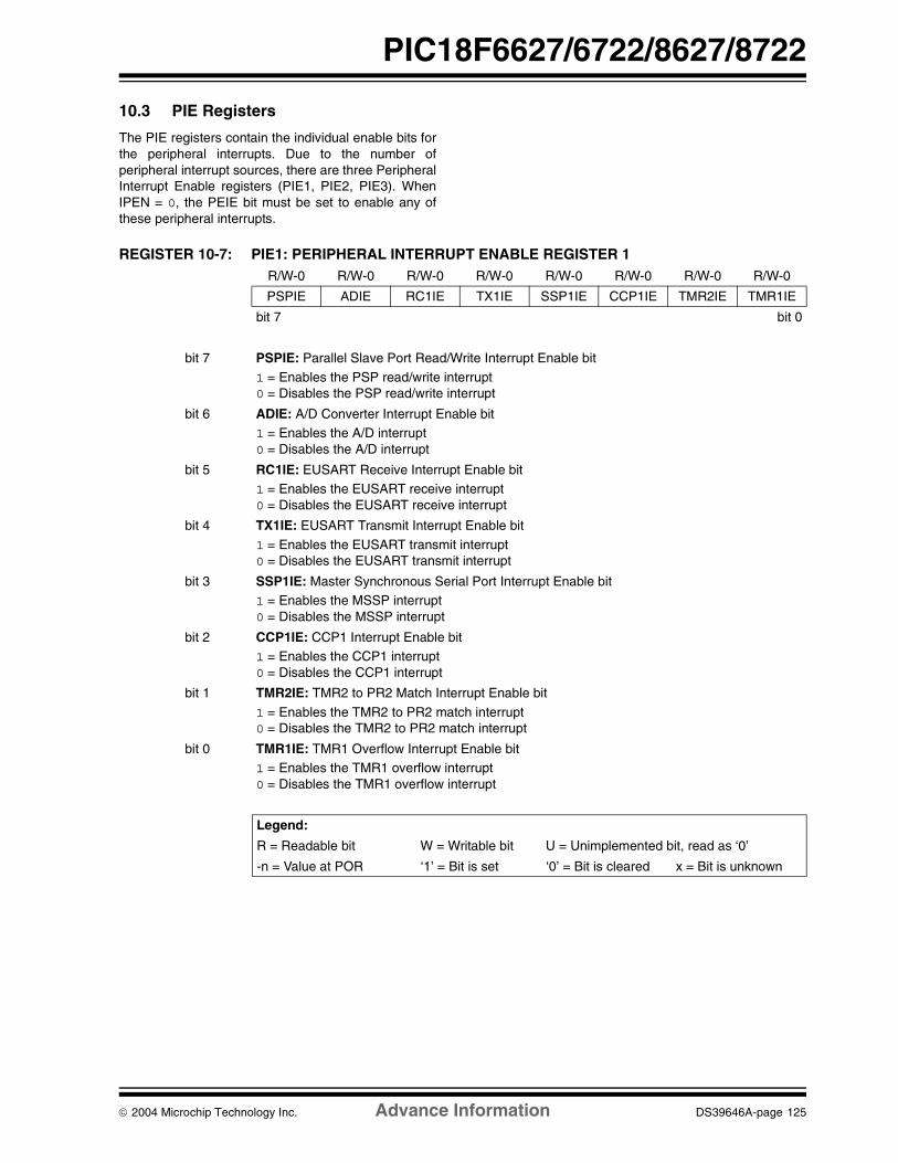
2004 Microchip Technology Inc. Advance Information DS39646A-page 125
PIC18F6627/6722/8627/8722
10.3 PIE Registers
The PIE registers contain the individual enable bits forthe peripheral interrupts. Due to the number ofperipheral interrupt sources, there are three PeripheralInterrupt Enable registers (PIE1, PIE2, PIE3). WhenIPEN = 0, the PEIE bit must be set to enable any ofthese peripheral interrupts.
REGISTER 10-7: PIE1: PERIPHERAL INTERRUPT ENABLE REGISTER 1 R/W-0 R/W-0 R/W-0 R/W-0 R/W-0 R/W-0 R/W-0 R/W-0
PSPIE ADIE RC1IE TX1IE SSP1IE CCP1IE TMR2IE TMR1IE
bit 7 bit 0
bit 7 PSPIE: Parallel Slave Port Read/Write Interrupt Enable bit
1 = Enables the PSP read/write interrupt 0 = Disables the PSP read/write interrupt
bit 6 ADIE: A/D Converter Interrupt Enable bit 1 = Enables the A/D interrupt 0 = Disables the A/D interrupt
bit 5 RC1IE: EUSART Receive Interrupt Enable bit1 = Enables the EUSART receive interrupt 0 = Disables the EUSART receive interrupt
bit 4 TX1IE: EUSART Transmit Interrupt Enable bit
1 = Enables the EUSART transmit interrupt 0 = Disables the EUSART transmit interrupt
bit 3 SSP1IE: Master Synchronous Serial Port Interrupt Enable bit1 = Enables the MSSP interrupt 0 = Disables the MSSP interrupt
bit 2 CCP1IE: CCP1 Interrupt Enable bit 1 = Enables the CCP1 interrupt 0 = Disables the CCP1 interrupt
bit 1 TMR2IE: TMR2 to PR2 Match Interrupt Enable bit
1 = Enables the TMR2 to PR2 match interrupt 0 = Disables the TMR2 to PR2 match interrupt
bit 0 TMR1IE: TMR1 Overflow Interrupt Enable bit1 = Enables the TMR1 overflow interrupt 0 = Disables the TMR1 overflow interrupt
Legend:
R = Readable bit W = Writable bit U = Unimplemented bit, read as ‘0’
-n = Value at POR ‘1’ = Bit is set ‘0’ = Bit is cleared x = Bit is unknown

PIC18F6627/6722/8627/8722
DS39646A-page 126 Advance Information 2004 Microchip Technology Inc.
REGISTER 10-8: PIE2: PERIPHERAL INTERRUPT ENABLE REGISTER 2 R/W-0 R/W-0 U-0 R/W-0 R/W-0 R/W-0 R/W-0 R/W-0
OSCFIE CMIE — EEIE BCL1IE HLVDIE TMR3IE CCP2IE
bit 7 bit 0
bit 7 OSCFIE: Oscillator Fail Interrupt Enable bit1 = Enabled0 = Disabled
bit 6 CMIE: Comparator Interrupt Enable bit
1 = Enabled0 = Disabled
bit 5 Unimplemented: Read as ‘0’
bit 4 EEIE: Interrupt Enable bit1 = Enabled0 = Disabled
bit 3 BCL1IE: Bus Collision Interrupt Enable bit
1 = Enabled0 = Disabled
bit 2 HLVDIE: High/Low-Voltage Detect Interrupt Enable bit 1 = Enabled0 = Disabled
bit 1 TMR3IE: TMR3 Overflow Interrupt Enable bit 1 = Enabled0 = Disabled
bit 0 CCP2IE: CCP2 Interrupt Enable bit
1 = Enabled0 = Disabled
Legend:
R = Readable bit W = Writable bit U = Unimplemented bit, read as ‘0’
-n = Value at POR ‘1’ = Bit is set ‘0’ = Bit is cleared x = Bit is unknown

2004 Microchip Technology Inc. Advance Information DS39646A-page 127
PIC18F6627/6722/8627/8722
REGISTER 10-9: PIE3: PERIPHERAL INTERRUPT ENABLE REGISTER 3 R/W-0 R/W-0 R-0 R-0 R/W-0 R/W-0 R/W-0 R/W-0
SSP2IE BCL2IE RC2IE TX2IE TMR4IE CCP5IE CCP4IE CCP3IE
bit 7 bit 0
bit 7 SSP2IE: Synchronous Serial Port2 Interrupt Enable bit1 = Enables the SSP2 interrupt0 = Disables the SSP2 interrupt
bit 6 BCL2IE: Bus Collision Interrupt Enable bit (MSSP2)
1 = Enabled0 = Disabled
bit 5 RC2IE: EUSART Receive Interrupt Enable bit 1 = Enabled0 = Disabled
bit 4 TX2IE: EUSART Transmit Interrupt Enable bit 1 = Enabled0 = Disabled
bit 3 TMR4IE: TMR4 to PR4 Match Interrupt Enable bit
1 = Enabled0 = Disabled
bit 2-0 CCP<5:3>IE: CCP<5:3> Interrupt Enable bit1 = Enabled0 = Disabled
Legend:
R = Readable bit W = Writable bit U = Unimplemented bit, read as ‘0’
-n = Value at POR ‘1’ = Bit is set ‘0’ = Bit is cleared x = Bit is unknown

PIC18F6627/6722/8627/8722
DS39646A-page 128 Advance Information 2004 Microchip Technology Inc.
10.4 IPR Registers
The IPR registers contain the individual priority bits forthe peripheral interrupts. Due to the number ofperipheral interrupt sources, there are three PeripheralInterrupt Priority registers (IPR1, IPR2, IPR3). Usingthe priority bits requires that the Interrupt PriorityEnable (IPEN) bit be set.
REGISTER 10-10: IPR1: PERIPHERAL INTERRUPT PRIORITY REGISTER 1 R/W-1 R/W-1 R/W-1 R/W-1 R/W-1 R/W-1 R/W-1 R/W-1
PSPIP ADIP RC1IP TX1IP SSP1IP CCP1IP TMR2IP TMR1IP
bit 7 bit 0
bit 7 PSPIP: Parallel Slave Port Read/Write Interrupt Priority bit 1 = High priority 0 = Low priority
bit 6 ADIP: A/D Converter Interrupt Priority bit1 = High priority 0 = Low priority
bit 5 RC1IP: EUSART Receive Interrupt Priority bit
1 = High priority 0 = Low priority
bit 4 TX1IP: EUSART Transmit Interrupt Priority bit
1 = High priority 0 = Low priority
bit 3 SSP1IP: Master Synchronous Serial Port Interrupt Priority bit
1 = High priority 0 = Low priority
bit 2 CCP1IP: CCP1 Interrupt Priority bit1 = High priority 0 = Low priority
bit 1 TMR2IP: TMR2 to PR2 Match Interrupt Priority bit 1 = High priority 0 = Low priority
bit 0 TMR1IP: TMR1 Overflow Interrupt Priority bit
1 = High priority 0 = Low priority
Legend:
R = Readable bit W = Writable bit U = Unimplemented bit, read as ‘0’
-n = Value at POR ‘1’ = Bit is set ‘0’ = Bit is cleared x = Bit is unknown

2004 Microchip Technology Inc. Advance Information DS39646A-page 129
PIC18F6627/6722/8627/8722
REGISTER 10-11: IPR2: PERIPHERAL INTERRUPT PRIORITY REGISTER 2 R/W-1 R/W-1 U-0 R/W-1 R/W-1 R/W-1 R/W-1 R/W-1
OSCFIP CMIP — EEIP BCL1IP HLVDIP TMR3IP CCP2IP
bit 7 bit 0
bit 7 OSCFIP: Oscillator Fail Interrupt Priority bit1 = High priority0 = Low priority
bit 6 CMIP: Comparator Interrupt Priority bit
1 = High priority0 = Low priority
bit 5 Unimplemented: Read as ‘0’
bit 4 EEIP: Interrupt Priority bit1 = High priority0 = Low priority
bit 3 BCL1IP: Bus Collision Interrupt Priority bit
1 = High priority0 = Low priority
bit 2 HLVDIP: High/Low-Voltage Detect Interrupt Priority bit 1 = High priority0 = Low priority
bit 1 TMR3IP: TMR3 Overflow Interrupt Priority bit 1 = High priority0 = Low priority
bit 0 CCP2IP: CCP2 Interrupt Priority bit
1 = High priority0 = Low priority
Legend:
R = Readable bit W = Writable bit U = Unimplemented bit, read as ‘0’
-n = Value at POR ‘1’ = Bit is set ‘0’ = Bit is cleared x = Bit is unknown

PIC18F6627/6722/8627/8722
DS39646A-page 130 Advance Information 2004 Microchip Technology Inc.
REGISTER 10-12: IPR3: PERIPHERAL INTERRUPT PRIORITY REGISTER 3 R/W-0 R/W-0 R/W-1 R/W-1 R/W-1 R/W-1 R/W-1 R/W-1
SSP2IP BCL2IP RC2IP TX2IP TMR4IP CCP5IP CCP4IP CCP3IP
bit 7 bit 0
bit 7 SSP2IP: Synchronous Serial Port2 Interrupt Priority bit1 = High priority0 = Low priority
bit 6 BCL2IP: Bus Collision Interrupt Priority bit (MSSP2)
1 = High priority0 = Low priority
bit 5 RC2IP: EUSART2 Receive Interrupt Priority bit1 = High priority0 = Low priority
bit 4 TX2IP: EUSART2 Transmit Interrupt Priority bit1 = High priority0 = Low priority
bit 3 TMR4IP: TMR4 to PR4 Match Interrupt Priority bit
1 = High priority0 = Low priority
bit 2-0 CCP<5:3>IP: CCP<5:3> Interrupt Priority bit1 = High priority0 = Low priority
Legend:
R = Readable bit W = Writable bit U = Unimplemented bit, read as ‘0’
-n = Value at POR ‘1’ = Bit is set ‘0’ = Bit is cleared x = Bit is unknown
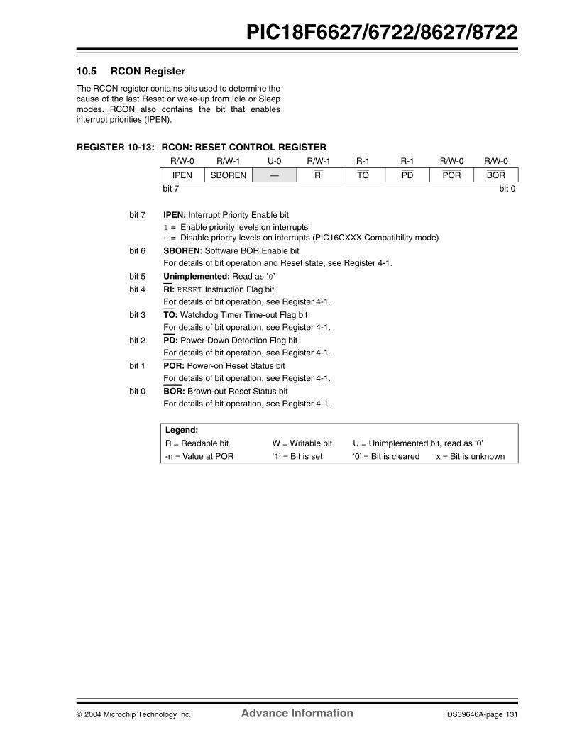
2004 Microchip Technology Inc. Advance Information DS39646A-page 131
PIC18F6627/6722/8627/8722
10.5 RCON Register
The RCON register contains bits used to determine thecause of the last Reset or wake-up from Idle or Sleepmodes. RCON also contains the bit that enablesinterrupt priorities (IPEN).
REGISTER 10-13: RCON: RESET CONTROL REGISTER R/W-0 R/W-1 U-0 R/W-1 R-1 R-1 R/W-0 R/W-0
IPEN SBOREN — RI TO PD POR BOR
bit 7 bit 0
bit 7 IPEN: Interrupt Priority Enable bit 1 = Enable priority levels on interrupts0 = Disable priority levels on interrupts (PIC16CXXX Compatibility mode)
bit 6 SBOREN: Software BOR Enable bitFor details of bit operation and Reset state, see Register 4-1.
bit 5 Unimplemented: Read as ‘0’
bit 4 RI: RESET Instruction Flag bit
For details of bit operation, see Register 4-1.
bit 3 TO: Watchdog Timer Time-out Flag bit
For details of bit operation, see Register 4-1.
bit 2 PD: Power-Down Detection Flag bit
For details of bit operation, see Register 4-1.
bit 1 POR: Power-on Reset Status bit
For details of bit operation, see Register 4-1.
bit 0 BOR: Brown-out Reset Status bit
For details of bit operation, see Register 4-1.
Legend:
R = Readable bit W = Writable bit U = Unimplemented bit, read as ‘0’
-n = Value at POR ‘1’ = Bit is set ‘0’ = Bit is cleared x = Bit is unknown

PIC18F6627/6722/8627/8722
DS39646A-page 132 Advance Information 2004 Microchip Technology Inc.
10.6 INTn Pin Interrupts
External interrupts on the RB0/INT0, RB1/INT1, RB2/INT2 and RB3/INT3 pins are edge-triggered. If thecorresponding INTEDGx bit in the INTCON2 register isset (= 1), the interrupt is triggered by a rising edge; ifthe bit is clear, the trigger is on the falling edge. Whena valid edge appears on the RBx/INTx pin, thecorresponding flag bit, INTxF, is set. This interrupt canbe disabled by clearing the corresponding enable bit,INTxE. Flag bit, INTxF, must be cleared in software inthe Interrupt Service Routine before re-enabling theinterrupt.
All external interrupts (INT0, INT1, INT2 and INT3) canwake-up the processor from the power-managedmodes if bit INTxE was set prior to going into power-managed modes. If the Global Interrupt Enable bit,GIE, is set, the processor will branch to the interruptvector following wake-up.
Interrupt priority for INT1, INT2 and INT3 is determinedby the value contained in the interrupt priority bits,INT1IP (INTCON3<6>), INT2IP (INTCON3<7>) andINT3IP (INTCON2<1>). There is no priority bitassociated with INT0. It is always a high priorityinterrupt source.
10.7 TMR0 Interrupt
In 8-bit mode (which is the default), an overflow in theTMR0 register (FFh → 00h) will set flag bit, TMR0IF. In16-bit mode, an overflow in the TMR0H:TMR0L registerpair (FFFFh → 0000h) will set TMR0IF. The interrupt canbe enabled/disabled by setting/clearing enable bit,TMR0IE (INTCON<5>). Interrupt priority for Timer0 isdetermined by the value contained in the interruptpriority bit, TMR0IP (INTCON2<2>). See Section 12.0“Timer0 Module” for further details on the Timer0module.
10.8 PORTB Interrupt-on-Change
An input change on PORTB<7:4> sets flag bit, RBIF(INTCON<0>). The interrupt can be enabled/disabledby setting/clearing enable bit, RBIE (INTCON<3>).Interrupt priority for PORTB interrupt-on-change isdetermined by the value contained in the interruptpriority bit, RBIP (INTCON2<0>).
10.9 Context Saving During Interrupts
During interrupts, the return PC address is saved onthe stack. Additionally, the WREG, Status and BSRregisters are saved on the fast return stack. If a fastreturn from interrupt is not used (see Section 5.3“Data Memory Organization”), the user may need tosave the WREG, Status and BSR registers on entry tothe Interrupt Service Routine. Depending on the user’sapplication, other registers may also need to be saved.Example 10-1 saves and restores the WREG, Statusand BSR registers during an Interrupt Service Routine.
EXAMPLE 10-1: SAVING STATUS, WREG AND BSR REGISTERS IN RAM MOVWF W_TEMP ; W_TEMP is in virtual bankMOVFF STATUS, STATUS_TEMP ; STATUS_TEMP located anywhereMOVFF BSR, BSR_TEMP ; BSR_TMEP located anywhere;; USER ISR CODE;MOVFF BSR_TEMP, BSR ; Restore BSRMOVF W_TEMP, W ; Restore WREGMOVFF STATUS_TEMP, STATUS ; Restore STATUS

2004 Microchip Technology Inc. Advance Information DS39646A-page 133
PIC18F6627/6722/8627/8722
11.0 I/O PORTS
Depending on the device selected and featuresenabled, there are up to nine ports available. Somepins of the I/O ports are multiplexed with an alternatefunction from the peripheral features on the device. Ingeneral, when a peripheral is enabled, that pin may notbe used as a general purpose I/O pin.
Each port has three registers for its operation. Theseregisters are:
• TRIS register (data direction register)• Port register (reads the levels on the pins of the
device)• LAT register (output latch)
The Data Latch (LAT register) is useful forread-modify-write operations on the value that the I/Opins are driving.
A simplified model of a generic I/O port, without theinterfaces to other peripherals, is shown in Figure 11-1.
FIGURE 11-1: GENERIC I/O PORT OPERATION
11.1 PORTA, TRISA and LATA Registers
PORTA is an 8-bit wide, bidirectional port. The corre-sponding data direction register is TRISA. Setting aTRISA bit (= 1) will make the corresponding PORTA pinan input (i.e., put the corresponding output driver in ahigh-impedance mode). Clearing a TRISA bit (= 0) willmake the corresponding PORTA pin an output (i.e., putthe contents of the output latch on the selected pin).
Reading the PORTA register reads the status of thepins, whereas writing to it, will write to the port latch.
The Data Latch register (LATA) is also memorymapped. Read-modify-write operations on the LATAregister read and write the latched output value forPORTA.
The RA4 pin is multiplexed with the Timer0 moduleclock input to become the RA4/T0CKI pin. Pins RA6and RA7 are multiplexed with the main oscillator pins;they are enabled as oscillator or I/O pins by the selec-tion of the main oscillator in the configuration register(see Section 25.1 “Configuration Bits” for details).When they are not used as port pins, RA6 and RA7 andtheir associated TRIS and LAT bits are read as ‘0’.
The other PORTA pins are multiplexed with the analogVREF+ and VREF- inputs. The operation of pinsRA5:RA0 as A/D converter inputs is selected byclearing or setting the PCFG3:PCFG0 control bits in theADCON1 register.
The RA4/T0CKI pin is a Schmitt Trigger input and anopen-drain output. All other PORTA pins have TTLinput levels and full CMOS output drivers.
The TRISA register controls the direction of the PORTApins, even when they are being used as analog inputs.The user must ensure the bits in the TRISA register aremaintained set when using them as analog inputs.
EXAMPLE 11-1: INITIALIZING PORTA
DataBus
WR LAT
WR TRIS
RD Port
Data Latch
TRIS Latch
RD TRIS
InputBuffer
I/O pin(1)
QD
CK
QD
CK
EN
Q D
EN
RD LAT
or Port
Note 1: I/O pins have diode protection to VDD and VSS.
Note: On a Power-on Reset, RA5 and RA3:RA0are configured as analog inputs and readas ‘0’. RA4 is configured as a digital input.
CLRF PORTA ; Initialize PORTA by; clearing output; data latches
CLRF LATA ; Alternate method; to clear output; data latches
MOVLW 0Fh ; Configure A/D MOVWF ADCON1 ; for digital inputsMOVWF 07h ; Configure comparatorsMOVWF CMCON ; for digital inputMOVLW 0CFh ; Value used to
; initialize data ; direction
MOVWF TRISA ; Set RA<3:0> as inputs; RA<5:4> as outputs

PIC18F6627/6722/8627/8722
DS39646A-page 134 Advance Information 2004 Microchip Technology Inc.
TABLE 11-1: PORTA FUNCTIONS
Pin Name FunctionTRIS
SettingI/O
I/O Type
Description
RA0/AN0 RA0 0 O DIG LATA<0> data output; not affected by analog input.
1 I TTL PORTA<0> data input; disabled when analog input enabled.
AN0 1 I ANA A/D input channel 0. Default input configuration on POR; does not affect digital output.
RA1/AN1 RA1 0 O DIG LATA<1> data output; not affected by analog input.
1 I TTL PORTA<1> data input; disabled when analog input enabled.
AN1 1 I ANA A/D input channel 1. Default input configuration on POR; does not affect digital output.
RA2/AN2/VREF- RA2 0 O DIG LATA<2> data output; not affected by analog input.
1 I TTL PORTA<2> data input. Disabled when analog functions enabled.
AN2 1 I ANA A/D input channel 2. Default input configuration on POR.
VREF- 1 I ANA Comparator voltage reference low input and A/D voltage reference low input.
RA3/AN3/VREF+ RA3 0 O DIG LATA<3> data output; not affected by analog input.
1 I TTL PORTA<3> data input; disabled when analog input enabled.
AN3 1 I ANA A/D input channel 3. Default input configuration on POR.
VREF+ 1 I ANA Comparator voltage reference high input and A/D voltage reference high input.
RA4/T0CKI RA4 0 O DIG LATA<4> data output
1 I ST PORTA<4> data input; default configuration on POR.
T0CKI x I ST Timer0 clock input.
RA5/AN4/HLVDIN RA5 0 O DIG LATA<5> data output; not affected by analog input.
1 I TTL PORTA<5> data input; disabled when analog input enabled.
AN4 1 I ANA A/D input channel 4. Default configuration on POR.
HLVDIN 1 I ANA High/Low-Voltage Detect external trip point input.
OSC2/CLKO/RA6 OSC2 x O ANA Main oscillator feedback output connection (XT, HS, HSPLL and LP modes).
CLKO x O DIG System cycle clock output (FOSC/4) in all oscillator modes except RC, INTIO7 and EC.
RA6 0 O DIG LATA<6> data output. Enabled in RCIO, INTIO2 and ECIO modes only.
1 I TTL PORTA<6> data input. Enabled in RCIO, INTIO2 and ECIO modes only.
OSC1/CLKI/RA7 OSC1 x I ANA Main oscillator input connection.
CLKI x I ANA Main clock input connection.
RA7 0 O DIG LATA<7> data output. Disabled in external oscillator modes.
1 I TTL PORTA<7> data input. Disabled in external oscillator modes.
Legend: PWR = Power Supply, O = Output, I = Input, ANA = Analog Signal, DIG = Digital Output, ST= Schmitt Buffer Input, TTL = TTL Buffer Input, x = Don’t care (TRIS bit does not affect port direction or is overridden for this option).

2004 Microchip Technology Inc. Advance Information DS39646A-page 135
PIC18F6627/6722/8627/8722
TABLE 11-2: SUMMARY OF REGISTERS ASSOCIATED WITH PORTA
Name Bit 7 Bit 6 Bit 5 Bit 4 Bit 3 Bit 2 Bit 1 Bit 0Reset Values
on Page
PORTA RA7(1) RA6(1) RA5 RA4 RA3 RA2 RA1 RA0 61
LATA LATA7(1) LATA6(1) LATA Data Output Register 60
TRISA TRISA7(1) TRISA6(1) PORTA Data Direction Register 60
ADCON1 — — VCFG1 VCFG0 PCFG3 PCFG2 PCFG1 PCFG0 59
Legend: — = unimplemented, read as ‘0’. Shaded cells are not used by PORTA.
Note 1: RA7:RA6 and their associated latch and data direction bits are enabled as I/O pins based on oscillator configuration; otherwise, they are read as ‘0’.

PIC18F6627/6722/8627/8722
DS39646A-page 136 Advance Information 2004 Microchip Technology Inc.
11.2 PORTB, TRISB and LATB Registers
PORTB is an 8-bit wide, bidirectional port. The corre-sponding data direction register is TRISB. Setting aTRISB bit (= 1) will make the corresponding PORTBpin an input (i.e., put the corresponding output driver ina high-impedance mode). Clearing a TRISB bit (= 0)will make the corresponding PORTB pin an output(i.e., put the contents of the output latch on the
selected pin).
The Data Latch register (LATB) is also memorymapped. Read-modify-write operations on the LATBregister read and write the latched output value forPORTB.
EXAMPLE 11-2: INITIALIZING PORTB
Each of the PORTB pins has a weak internal pull-up. Asingle control bit can turn on all the pull-ups. This isperformed by clearing bit RBPU (INTCON2<7>). Theweak pull-up is automatically turned off when the portpin is configured as an output. The pull-ups aredisabled on a Power-on Reset.
Four of the PORTB pins (RB7:RB4) have aninterrupt-on-change feature. Only pins configured asinputs can cause this interrupt to occur (i.e., anyRB7:RB4 pin configured as an output is excluded fromthe interrupt-on-change comparison). The input pins (ofRB7:RB4) are compared with the old value latched onthe last read of PORTB. The “mismatch” outputs ofRB7:RB4 are ORed together to generate the RB PortChange Interrupt with Flag bit, RBIF (INTCON<0>).
This interrupt can wake the device frompower-managed modes. The user, in the InterruptService Routine, can clear the interrupt in the followingmanner:
a) Any read or write of PORTB (except with theMOVSF, MOVSS, MOVFF (ANY), PORTBinstruction). This will end the mismatchcondition.
b) Clear flag bit RBIF.
A mismatch condition will continue to set flag bit RBIF.Reading PORTB will end the mismatch condition andallow flag bit RBIF to be cleared.
The interrupt-on-change feature is recommended forwake-up on key depression operation and operationswhere PORTB is only used for the interrupt-on-changefeature. Polling of PORTB is not recommended whileusing the interrupt-on-change feature.
For 80-pin devices, RB3 can be configured as thealternate peripheral pin for the CCP2 module byclearing the CCP2MX configuration bit. This appliesonly when the device is in one of the operating modesother than the default Microcontroller mode. If thedevice is in Microcontroller mode, the alternateassignment for CCP2 is RE7. As with other CCP2 con-figurations, the user must ensure that the TRISB<3> bitis set appropriately for the intended operation.
CLRF PORTB ; Initialize PORTB by; clearing output; data latches
CLRF LATB ; Alternate method; to clear output; data latches
MOVLW 0CFh ; Value used to; initialize data ; direction
MOVWF TRISB ; Set RB<3:0> as inputs; RB<5:4> as outputs; RB<7:6> as inputs

2004 Microchip Technology Inc. Advance Information DS39646A-page 137
PIC18F6627/6722/8627/8722
TABLE 11-3: PORTB FUNCTIONS
Pin Name FunctionTRIS
SettingI/O
I/O Type
Description
RB0/INT0/FLT0 RB0 0 O DIG LATB<0> data output.
1 I TTL PORTB<0> data input; weak pull-up when RBPU bit is cleared.
INT0 1 I ST External Interrupt 0 input.
FLT0 1 I ST ECCPx PWM fault input, enabled in software.
RB1/INT1 RB1 0 O DIG LATB<1> data output.
1 I TTL PORTB<1> data input; weak pull-up when RBPU bit is cleared.
INT1 1 I ST External Interrupt 1 input.
RB2/INT2 RB2 0 O DIG LATB<2> data output.
1 I TTL PORTB<2> data input; weak pull-up when RBPU bit is cleared.
INT2 1 I ST External Interrupt 2 input.
RB3/INT3/CCP2/P2A
RB3 0 O DIG LATB<3> data output.
1 I TTL PORTB<3> data input; weak pull-up when RBPU bit is cleared and capture input is disabled.
INT3 1 I ST External Interrupt 3 input.
CCP2(1) 0 O DIG ECCP2 compare output and ECCP2 PWM output. Takes priority over port data.
1 I ST ECCP2 capture input.
P2A 0 O DIG ECCP2 Enhanced PWM output, channel A. May be configured for tri-state during enhanced PWM shutdown events. Takes priority over port data.
RB4/KBI0 RB4 0 O DIG LATB<4> data output.
1 I TTL PORTB<4> data input; weak pull-up when RBPU bit is cleared.
KBI0 1 I TTL Interrupt-on-pin change.
RB5/KBI1/PGM RB5 0 O DIG LATB<5> data output
1 I TTL PORTB<5> data input; weak pull-up when RBPU bit is cleared.
KBI1 1 I TTL Interrupt-on-pin change.
PGM x I ST Single-Supply Programming mode entry (ICSP). Enabled by LVP configuration bit; all other pin functions disabled.
RB6/KBI2/PGC RB6 0 O DIG LATB<6> data output
1 I TTL PORTB<6> data input; weak pull-up when RBPU bit is cleared.
KBI2 1 I TTL Interrupt-on-pin change.
PGC x I ST Serial execution (ICSP™) clock input for ICSP and ICD operation(2).
RB7/KBI3/PGD RB7 0 O DIG LATB<7> data output.
1 I TTL PORTB<7> data input; weak pull-up when RBPU bit is cleared.
KBI3 1 I TTL Interrupt-on-pin change.
PGD x O DIG Serial execution data output for ICSP and ICD operation(2).
x I ST Serial execution data input for ICSP and ICD operation(2).
Legend: PWR = Power Supply, O = Output, I = Input, ANA = Analog Signal, DIG = Digital Output, ST = Schmitt Buffer Input, TTL = TTL Buffer Input, x = Don’t care (TRIS bit does not affect port direction or is overridden for this option).
Note 1: Alternate assignment for CCP2 when the CCP2MX configuration bit is cleared (Microprocessor, Extended Microcontroller and Microcontroller with Boot Block modes, 80-pin devices only). Default assignment is RC1.
2: All other pin functions are disabled when ICSP or ICD operations are enabled.

PIC18F6627/6722/8627/8722
DS39646A-page 138 Advance Information 2004 Microchip Technology Inc.
TABLE 11-4: SUMMARY OF REGISTERS ASSOCIATED WITH PORTB
Name Bit 7 Bit 6 Bit 5 Bit 4 Bit 3 Bit 2 Bit 1 Bit 0Reset Values
on Page
PORTB RB7 RB6 RB5 RB4 RB3 RB2 RB1 RB0 60
LATB LATB Data Output Register 60
TRISB PORTB Data Direction Register 60
INTCON GIE/GIEH PEIE/GIEL TMR0IE INT0IE RBIE TMR0IF INT0IF RBIF 57
INTCON2 RBPU INTEDG0 INTEDG1 INTEDG2 INTEDG3 TMR0IP INT3IP RBIP 57
INTCON3 INT2IP INT1IP INT3IE INT2IE INT1IE INT3IF INT2IF INT1IF 57
Legend: Shaded cells are not used by PORTB.

2004 Microchip Technology Inc. Advance Information DS39646A-page 139
PIC18F6627/6722/8627/8722
11.3 PORTC, TRISC and LATC Registers
PORTC is an 8-bit wide, bidirectional port. The corre-sponding data direction register is TRISC. Setting aTRISC bit (= 1) will make the corresponding PORTCpin an input (i.e., put the corresponding output driver ina High-Impedance mode). Clearing a TRISC bit (= 0)will make the corresponding PORTC pin an output(i.e., put the contents of the output latch on the
selected pin).
The Data Latch register (LATC) is also memorymapped. Read-modify-write operations on the LATCregister read and write the latched output value forPORTC.
PORTC is multiplexed with several peripheral functions(Table ). The pins have Schmitt Trigger input buffers.RC1 is normally configured by configuration bitCCP2MX as the default peripheral pin of the CCP2module (default/erased state, CCP2MX = 1).
When enabling peripheral functions, care should betaken in defining TRIS bits for each PORTC pin. Someperipherals override the TRIS bit to make a pin an output,while other peripherals override the TRIS bit to make apin an input. The user should refer to the correspondingperipheral section for the correct TRIS bit settings.
The contents of the TRISC register are affected byperipheral overrides. Reading TRISC always returnsthe current contents, even though a peripheral devicemay be overriding one or more of the pins.
EXAMPLE 11-3: INITIALIZING PORTC
Note: On a Power-on Reset, these pins areconfigured as digital inputs.
CLRF PORTC ; Initialize PORTC by; clearing output; data latches
CLRF LATC ; Alternate method; to clear output; data latches
MOVLW 0CFh ; Value used to ; initialize data ; direction
MOVWF TRISC ; Set RC<3:0> as inputs; RC<5:4> as outputs; RC<7:6> as inputs

PIC18F6627/6722/8627/8722
DS39646A-page 140 Advance Information 2004 Microchip Technology Inc.
TABLE 11-5: PORTC FUNCTIONS
Pin Name FunctionTRIS
SettingI/O I/O Type Description
RC0/T1OSO/T13CKI RC0 0 O DIG LATC<0> data output.
1 I ST PORTC<0> data input.
T1OSO x O ANA Timer1 oscillator output; enabled when Timer1 oscillator enabled. Disables digital I/O.
T13CKI 1 I ST Timer1/Timer3 counter input.
RC1/T1OSI/CCP2/P2A
RC1 0 O DIG LATC<1> data output.
1 I ST PORTC<1> data input.
T1OSI x I ANA Timer1 oscillator input; enabled when Timer1 oscillator enabled. Disables digital I/O.
CCP2(1) 0 O DIG ECCP2 compare output and ECCP2 PWM output. Takes priority over port data.
1 I ST ECCP2 capture input
P2A 0 O DIG ECCP2 Enhanced PWM output, channel A. May be configured for tri-state during enhanced PWM shutdown events. Takes priority over port data.
RC2/CCP1/P1A RC2 0 O DIG LATC<2> data output.
1 I ST PORTC<2> data input.
CCP1 0 O DIG ECCP1 compare output and ECCP1 PWM output. Takes priority over port data.
1 I ST ECCP1 capture input.
P1A 0 O DIG ECCP1 Enhanced PWM output, channel A. May be configured for tri-state during enhanced PWM shutdown events. Takes priority over port data.
RC3/SCK1/SCL1 RC3 0 O DIG LATC<3> data output.
1 I ST PORTC<3> data input.
SCK1 0 O DIG SPI™ clock output (MSSP module). Takes priority over port data.
1 I ST SPI clock input (MSSP module).
SCL1 0 O DIG I2C™ clock output (MSSP module). Takes priority over port data.
1 I I2C/SMB I2C clock input (MSSP module); input type depends on module setting.
RC4/SDI1/SDA1 RC4 0 O DIG LATC<4> data output.
1 I ST PORTC<4> data input.
SDI1 1 I ST SPI data input (MSSP module).
SDA1 1 O DIG I2C data output (MSSP module). Takes priority over port data.
1 I I2C/SMB I2C data input (MSSP module); input type depends on module setting.
RC5/SDO1 RC5 0 O DIG LATC<5> data output.
1 I ST PORTC<5> data input.
SDO1 0 O DIG SPI data output (MSSP module). Takes priority over port data.
Legend: DIG = Digital level output; TTL = TTL input buffer; ST = Schmitt Trigger input buffer; ANA = Analog level input/output; I2C/SMB = I2C/SMBus input buffer; x = Don’t care (TRIS bit does not affect port direction or is overridden for this option).
Note 1: Default assignment for CCP2 when CCP2MX configuration bit is set.

2004 Microchip Technology Inc. Advance Information DS39646A-page 141
PIC18F6627/6722/8627/8722
TABLE 11-6: SUMMARY OF REGISTERS ASSOCIATED WITH PORTC
RC6/TX1/CK1 RC6 0 O DIG LATC<6> data output.
1 I ST PORTC<6> data input.
TX1 0 O DIG Asynchronous serial transmit data output (EUSART module). Takes priority over port data.
CK1 0 O DIG Synchronous serial clock output (EUSART module). Takes priority over port data.
1 I ST Synchronous serial clock input (EUSART module).
RC7/RX1/DT1 RC7 0 O DIG LATC<7> data output.
1 I ST PORTC<7> data input.
RX1 1 I ST Asynchronous serial receive data input (EUSART module)
DT1 1 O DIG Synchronous serial data output (EUSART module). Takes priority over port data. User must configure as input.
1 I ST Synchronous serial data input (EUSART module). User must configure as an input.
TABLE 11-5: PORTC FUNCTIONS (CONTINUED)
Pin Name FunctionTRIS
SettingI/O I/O Type Description
Legend: DIG = Digital level output; TTL = TTL input buffer; ST = Schmitt Trigger input buffer; ANA = Analog level input/output; I2C/SMB = I2C/SMBus input buffer; x = Don’t care (TRIS bit does not affect port direction or is overridden for this option).
Note 1: Default assignment for CCP2 when CCP2MX configuration bit is set.
Name Bit 7 Bit 6 Bit 5 Bit 4 Bit 3 Bit 2 Bit 1 Bit 0Reset Values
on Page
PORTC RC7 RC6 RC5 RC4 RC3 RC2 RC1 RC0 60
LATC LATC Data Output Register 60
TRISC PORTC Data Direction Register 60
Legend: Shaded cells are not used by PORTC.

PIC18F6627/6722/8627/8722
DS39646A-page 142 Advance Information 2004 Microchip Technology Inc.
11.4 PORTD, TRISD and LATD Registers
PORTD is an 8-bit wide, bidirectional port. The corre-sponding data direction register is TRISD. Setting aTRISD bit (= 1) will make the corresponding PORTDpin an input (i.e., put the corresponding output driver ina High-Impedance mode). Clearing a TRISD bit (= 0)will make the corresponding PORTD pin an output(i.e., put the contents of the output latch on the
selected pin).
The Data Latch register (LATD) is also memorymapped. Read-modify-write operations on the LATDregister read and write the latched output value forPORTD.
All pins on PORTD are implemented with SchmittTrigger input buffers. Each pin is individuallyconfigurable as an input or output.
In 80-pin devices, PORTD is multiplexed with thesystem bus as part of the external memory interface.I/O port and other functions are only available when theinterface is disabled by setting the EBDIS bit(MEMCON<7>). When the interface is enabled,PORTD is the low-order byte of the multiplexedaddress/data bus (AD7:AD0). The TRISD bits are alsooverridden.
PORTD can also be configured to function as an 8-bitwide parallel microprocessor port by setting thePSPMODE control bit (PSPCON<4>). In this mode,parallel port data takes priority over other digital I/O (butnot the external memory interface). When the parallelport is active, the input buffers are TTL. For moreinformation, refer to Section 11.10 “Parallel SlavePort”.
EXAMPLE 11-4: INITIALIZING PORTD
Note: On a Power-on Reset, these pins areconfigured as digital inputs.
CLRF PORTD ; Initialize PORTD by ; clearing output ; data latchesCLRF LATD ; Alternate method
; to clear output; data latches
MOVLW 0CFh ; Value used to ; initialize data ; direction
MOVWF TRISD ; Set RD<3:0> as inputs; RD<5:4> as outputs; RD<7:6> as inputs

2004 Microchip Technology Inc. Advance Information DS39646A-page 143
PIC18F6627/6722/8627/8722 TABLE 11-7: PORTD FUNCTIONS
Pin Name FunctionTRIS
SettingI/O I/O Type Description
RD0/AD0/PSP0 RD0 0 O DIG LATD<0> data output.
1 I ST PORTD<0> data input.
AD0(1) x O DIG External memory interface, address/data bit 0 output. Takes priority over PSP and port data.
x I TTL External memory interface, data bit 0 input.
PSP0 x O DIG PSP read data output (LATD<0>). Takes priority over port data.
x I TTL PSP write data input.
RD1/AD1/PSP1 RD1 0 O DIG LATD<1> data output.
1 I ST PORTD<1> data input.
AD1(1) x O DIG External memory interface, address/data bit 1 output. Takes priority over PSP and port data.
x I TTL External memory interface, data bit 1 input.
PSP1 x O DIG PSP read data output (LATD<1>). Takes priority over port data.
x I TTL PSP write data input.
RD2/AD2/PSP2 RD2 0 O DIG LATD<2> data output.
1 I ST PORTD<2> data input.
AD2(1) x O DIG External memory interface, address/data bit 2 output. Takes priority over PSP and port data.
x I TTL External memory interface, data bit 2 input.
PSP2 x O DIG PSP read data output (LATD<2>). Takes priority over port data.
x I TTL PSP write data input.
RD3/AD3/PSP3 RD3 0 O DIG LATD<3> data output.
1 I ST PORTD<3> data input.
AD3(1) x O DIG External memory interface, address/data bit 3 output. Takes priority over PSP and port data.
x I TTL External memory interface, data bit 3 input.
PSP3 x O DIG PSP read data output (LATD<3>). Takes priority over port data.
x I TTL PSP write data input.
RD4/AD4/PSP4/SDO2
RD4 0 O DIG LATD<4> data output.
1 I ST PORTD<4> data input.
AD4(1) x O DIG External memory interface, address/data bit 4 output. Takes priority over PSP, MSSP and port data.
x I TTL External memory interface, data bit 4 input.
PSP4 x O DIG PSP read data output (LATD<4>). Takes priority over port and PSP data.
x I TTL PSP write data input.
SDO2 0 O DIG SPI™ data output (MSSP module). Takes priority over PSP and port data.
Legend: PWR = Power Supply, O = Output, I = Input, ANA = Analog Signal, DIG = Digital Output, ST = Schmitt Buffer Input, TTL = TTL Buffer Input, x = Don’t care (TRIS bit does not affect port direction or is overridden for this option).
Note 1: Implemented on 80-pin devices only.

PIC18F6627/6722/8627/8722
DS39646A-page 144 Advance Information 2004 Microchip Technology Inc.
TABLE 11-8: SUMMARY OF REGISTERS ASSOCIATED WITH PORTD
RD5/AD5/PSP5/SDI2/SDA2
RD5 0 O DIG LATD<5> data output.
1 I ST PORTD<5> data input.
AD5(1) x O DIG External memory interface, address/data bit 5 output. Takes priority over PSP, MSSP and port data.
x I TTL External memory interface, data bit 5 input.
PSP5 x O DIG PSP read data output (LATD<5>). Takes priority over port data.
x I TTL PSP write data input.
SDI2 1 I ST SPI data input (MSSP module).
SDA2 1 O DIG I2C™ data output (MSSP module). Takes priority over PSP and port data.
1 I I2C/SMB I2C data input (MSSP module); input type depends on module setting.
RD6/AD6/PSP6/SCK2/SCL2
RD6 0 O DIG LATD<6> data output.
1 I ST PORTD<6> data input.
AD6(1) x O DIG-3 External memory interface, address/data bit 6 output. Takes priority over PSP, MSSP and port data.
x I TTL External memory interface, data bit 6 input.
PSP6 x O DIG PSP read data output (LATD<6>). Takes priority over port data.
x I TTL PSP write data input.
SCK2 0 O DIG SPI clock output (MSSP module). Takes priority over PSP and port data.
1 I ST SPI clock input (MSSP module).
SCL2 0 O DIG I2C clock output (MSSP module). Takes priority over PSP and port data.
1 I I2C/SMB I2C clock input (MSSP module); input type depends on module setting.
RD7/AD7/PSP7/SS2
RD7 0 O DIG LATD<7> data output.
1 I ST PORTD<7> data input.
AD7(1) x O DIG External memory interface, address/data bit 7 output. Takes priority over PSP and port data.
x I TTL External memory interface, data bit 7 input.
PSP7 x O DIG PSP read data output (LATD<7>). Takes priority over port data.
x I TTL PSP write data input.
SS2 1 I TTL Slave select input for SSP (MSSP module).
Name Bit 7 Bit 6 Bit 5 Bit 4 Bit 3 Bit 2 Bit 1 Bit 0Reset Values
on Page
PORTD RD7 RD6 RD5 RD4 RD3 RD2 RD1 RD0 60
LATD LATD Data Output Register 60
TRISD PORTD Data Direction Register 60
TABLE 11-7: PORTD FUNCTIONS (CONTINUED)
Pin Name FunctionTRIS
SettingI/O I/O Type Description
Legend: PWR = Power Supply, O = Output, I = Input, ANA = Analog Signal, DIG = Digital Output, ST = Schmitt Buffer Input, TTL = TTL Buffer Input, x = Don’t care (TRIS bit does not affect port direction or is overridden for this option).
Note 1: Implemented on 80-pin devices only.

2004 Microchip Technology Inc. Advance Information DS39646A-page 145
PIC18F6627/6722/8627/8722
11.5 PORTE, TRISE and LATE Registers
PORTE is an 8-bit wide, bidirectional port. Thecorresponding data direction register is TRISE. Settinga TRISE bit (= 1) will make the corresponding PORTEpin an input (i.e., put the corresponding output driver ina high-impedance mode). Clearing a TRISE bit (= 0)will make the corresponding PORTE pin an output(i.e., put the contents of the output latch on the
selected pin).
The Data Latch register (LATE) is also memorymapped. Read-modify-write operations on the LATEregister read and write the latched output value forPORTE.
All pins on PORTE are implemented with SchmittTrigger input buffers. Each pin is individuallyconfigurable as an input or output.
When the device is operating in Microcontroller mode,pin RE7 can be configured as the alternate peripheralpin for the CCP2 module. This is done by clearing theCCP2MX configuration bit.
In 80-pin devices, PORTE is multiplexed with thesystem bus as part of the external memory interface.I/O port and other functions are only available when theinterface is disabled by setting the EBDIS bit(MEMCON<7>). When the interface is enabled (80-pindevices only), PORTE is the high-order byte of themultiplexed address/data bus (AD15:AD8). The TRISEbits are also overridden.
When the Parallel Slave Port is active on PORTD, threeof the PORTE pins (RE0/AD8/RD/P2D,RE1/AD9/WR/P2C and RE2/AD10/CS/P2B) are config-ured as digital control inputs for the port. The controlfunctions are summarized in Table 11-9. The reconfigu-ration occurs automatically when the PSPMODE controlbit (PSPCON<4>) is set. Users must still make certainthe the corresponding TRISE bits are set to configurethese pins as digital inputs.
EXAMPLE 11-5: INITIALIZING PORTE
Note: On a Power-on Reset, these pins areconfigured as digital inputs.
CLRF PORTE ; Initialize PORTE by; clearing output; data latches
CLRF LATE ; Alternate method; to clear output; data latches
MOVLW 03h ; Value used to ; initialize data ; direction
MOVWF TRISE ; Set RE<1:0> as inputs; RE<7:2> as outputs
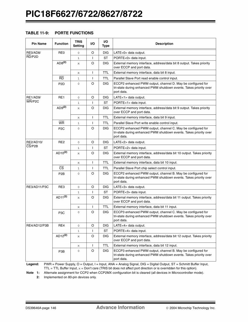
PIC18F6627/6722/8627/8722
DS39646A-page 146 Advance Information 2004 Microchip Technology Inc.
TABLE 11-9: PORTE FUNCTIONS
Pin Name FunctionTRIS
SettingI/O
I/O Type
Description
RE0/AD8/RD/P2D
RE0 0 O DIG LATE<0> data output.
1 I ST PORTE<0> data input.
AD8(2) x O DIG External memory interface, address/data bit 8 output. Takes priority over ECCP and port data.
x I TTL External memory interface, data bit 8 input.
RD 1 I TTL Parallel Slave Port read enable control input.
P2D 0 O DIG ECCP2 enhanced PWM output, channel D. May be configured for tri-state during enhanced PWM shutdown events. Takes priority over port data.
RE1/AD9/WR/P2C
RE1 0 O DIG LATE<1> data output.
1 I ST PORTE<1> data input.
AD9(2) x O DIG External memory interface, address/data bit 9 output. Takes priority over ECCP and port data.
x I TTL External memory interface, data bit 9 input.
WR 1 I TTL Parallel Slave Port write enable control input.
P2C 0 O DIG ECCP2 enhanced PWM output, channel C. May be configured for tri-state during enhanced PWM shutdown events. Takes priority over port data.
RE2/AD10/CS/P2B
RE2 0 O DIG LATE<2> data output.
1 I ST PORTE<2> data input.
AD10(2) x O DIG External memory interface, address/data bit 10 output. Takes priority over ECCP and port data.
x I TTL External memory interface, data bit 10 input.
CS 1 I TTL Parallel Slave Port chip select control input.
P2B 0 O DIG ECCP2 enhanced PWM output, channel B. May be configured for tri-state during enhanced PWM shutdown events. Takes priority over port data.
RE3/AD11/P3C RE3 0 O DIG LATE<3> data output.
1 I ST PORTE<3> data input.
AD11(2) x O DIG External memory interface, address/data bit 11 output. Takes priority over ECCP and port data.
x I TTL External memory interface, data bit 11 input.
P3C 0 O DIG ECCP3 enhanced PWM output, channel C. May be configured for tri-state during enhanced PWM shutdown events. Takes priority over port data.
RE4/AD12/P3B RE4 0 O DIG LATE<4> data output.
1 I ST PORTE<4> data input.
AD12(2) x O DIG External memory interface, address/data bit 12 output. Takes priority over ECCP and port data.
x I TTL External memory interface, data bit 12 input.
P3B 0 O DIG ECCP3 enhanced PWM output, channel B. May be configured for tri-state during enhanced PWM shutdown events. Takes priority over port data.
Legend: PWR = Power Supply, O = Output, I = Input, ANA = Analog Signal, DIG = Digital Output, ST = Schmitt Buffer Input, TTL = TTL Buffer Input, x = Don’t care (TRIS bit does not affect port direction or is overridden for this option).
Note 1: Alternate assignment for CCP2 when CCP2MX configuration bit is cleared (all devices in Microcontroller mode).2: Implemented on 80-pin devices only.

2004 Microchip Technology Inc. Advance Information DS39646A-page 147
PIC18F6627/6722/8627/8722
TABLE 11-10: SUMMARY OF REGISTERS ASSOCIATED WITH PORTE
RE5/AD13/P1C RE5 0 O DIG LATE<5> data output.
1 I ST PORTE<5> data input.
AD13(2) x O DIG External memory interface, address/data bit 13 output. Takes priority over ECCP and port data.
x I TTL External memory interface, data bit 13 input.
P1C 0 O DIG ECCP1 enhanced PWM output, channel C. May be configured for tri-state during enhanced PWM shutdown events. Takes priority over port data.
RE6/AD14/P1B RE6 0 O DIG LATE<6> data output.
1 I ST PORTE<6> data input.
AD14(2) x O DIG External memory interface, address/data bit 14 output. Takes priority over ECCP and port data.
x I TTL External memory interface, data bit 14 input.
P1B 0 O DIG ECCP1 enhanced PWM output, channel B. May be configured for tri-state during enhanced PWM shutdown events. Takes priority over port data.
RE7/AD15/CCP2/P2A
RE7 0 O DIG LATE<7> data output.
1 I ST PORTE<7> data input.
AD15(2) x O DIG External memory interface, address/data bit 15 output. Takes priority over ECCP and port data.
x I TTL External memory interface, data bit 15 input.
CCP2(1) 0 O DIG ECCP2 compare output and ECCP2 PWM output. Takes priority over port data.
1 I ST ECCP2 capture input.
P2A 0 O DIG ECCP2 enhanced PWM output, channel A. Takes priority over port and data. May be configured for tri-state during enhanced PWM shutdown events.
Name Bit 7 Bit 6 Bit 5 Bit 4 Bit 3 Bit 2 Bit 1 Bit 0Reset Values
on Page
PORTE RE7 RE6 RE5 RE4 RE3 RE2 RE1 RE0 60
LATE LATE Data Output Register 60
TRISE PORTE Data Direction bits 60
Legend: — = unimplemented, read as ‘0’. Shaded cells are not used by PORTE.
TABLE 11-9: PORTE FUNCTIONS (CONTINUED)
Pin Name FunctionTRIS
SettingI/O
I/O Type
Description
Legend: PWR = Power Supply, O = Output, I = Input, ANA = Analog Signal, DIG = Digital Output, ST = Schmitt Buffer Input, TTL = TTL Buffer Input, x = Don’t care (TRIS bit does not affect port direction or is overridden for this option).
Note 1: Alternate assignment for CCP2 when CCP2MX configuration bit is cleared (all devices in Microcontroller mode).2: Implemented on 80-pin devices only.

PIC18F6627/6722/8627/8722
DS39646A-page 148 Advance Information 2004 Microchip Technology Inc.
11.6 PORTF, LATF and TRISF Registers
PORTF is an 8-bit wide, bidirectional port. The corre-sponding data direction register is TRISF. Setting aTRISF bit (= 1) will make the corresponding PORTF pinan input (i.e., put the corresponding output driver in ahigh-impedance mode). Clearing a TRISF bit (= 0) willmake the corresponding PORTF pin an output (i.e., putthe contents of the output latch on the selected pin).
The Data Latch register (LATF) is also memorymapped. Read-modify-write operations on the LATFregister read and write the latched output value forPORTF.
All pins on PORTF are implemented with SchmittTrigger input buffers. Each pin is individuallyconfigurable as an input or output.
PORTF is multiplexed with several analog peripheralfunctions, including the A/D converter and comparatorinputs, as well as the comparator outputs. Pins RF1through RF2 may be used as comparator inputs oroutputs by setting the appropriate bits in the CMCONregister. To use RF0:RF6 as digital inputs, it is alsonecessary to turn off the A/D inputs.
EXAMPLE 11-6: INITIALIZING PORTF
Note: On a Power-on Reset, RA5 and RA3:RA0are configured as analog inputs and readas ‘0’. RA4 is configured as a digital input.
Note 1: On a Power-on Reset, the RF6:RF0 pinsare configured as Analog inputs and readas ‘0’.
2: To configure PORTF as digital I/O, set theADCON1 register.
CLRF PORTF ; Initialize PORTF by; clearing output; data latches
CLRF LATF ; Alternate method; to clear output; data latches
MOVLW 0x0F ; MOVWF ADCON1 ; Set PORTF as digital I/OMOVLW 0xCF ; Value used to
; initialize data ; direction
MOVWF TRISF ; Set RF3:RF0 as inputs; RF5:RF4 as outputs ; RF7:RF6 as inputs

2004 Microchip Technology Inc. Advance Information DS39646A-page 149
PIC18F6627/6722/8627/8722
TABLE 11-11: PORTF FUNCTIONS
TABLE 11-12: SUMMARY OF REGISTERS ASSOCIATED WITH PORTF
Pin Name FunctionTRIS
SettingI/O
I/O Type
Description
RF0/AN5 RF0 0 O DIG LATF<0> data output; not affected by analog input.
1 I ST PORTF<0> data input; disabled when analog input enabled.
AN5 1 I ANA A/D input channel 5. Default configuration on POR.
RF1/AN6/C2OUT RF1 0 O DIG LATF<1> data output; not affected by analog input.
1 I ST PORTF<1> data input; disabled when analog input enabled.
AN6 1 I ANA A/D input channel 6. Default configuration on POR.
C2OUT 0 O DIG Comparator 2 output; takes priority over port data.
RF2/AN7/C1OUT RF2 0 O DIG LATF<2> data output; not affected by analog input.
1 I ST PORTF<2> data input; disabled when analog input enabled.
AN7 1 I ANA A/D input channel 7. Default configuration on POR.
C1OUT 0 O TTL Comparator 1 output; takes priority over port data.
RF3/AN8 RF3 0 O DIG LATF<3> data output; not affected by analog input.
1 I ST PORTF<3> data input; disabled when analog input enabled.
AN8 1 I ANA A/D input channel 8 and Comparator C2+ input. Default input configuration on POR; not affected by analog output.
RF4/AN9 RF4 0 O DIG LATF<4> data output; not affected by analog input.
1 I ST PORTF<4> data input; disabled when analog input enabled.
AN9 1 I ANA A/D input channel 9 and Comparator C2- input. Default input configuration on POR; does not affect digital output.
RF5/AN10/CVREF RF5 0 O DIG LATF<5> data output; not affected by analog input. Disabled when CVREF output enabled.
1 I ST PORTF<5> data input; disabled when analog input enabled. Disabled when CVREF output enabled
AN10 1 I ANA A/D input channel 10 and Comparator C1+ input. Default input configuration on POR; not affected by analog output.
CVREF x O ANA Comparator voltage reference output. Enabling this feature disables digital I/O.
RF6/AN11 RF6 0 O DIG LATF<6> data output; not affected by analog input.
1 I ST PORTF<6> data input; disabled when analog input enabled.
AN11 1 I ANA A/D input channel 11 and Comparator C1- input. Default input configuration on POR; does not affect digital output.
RF7/SS1 RF7 0 O DIG LATF<7> data output.
1 I ST PORTF<7> data input.
SS1 1 I TTL Slave select input for SSP (MSSP module).
Legend: PWR = Power Supply, O = Output, I = Input, ANA = Analog Signal, DIG = Digital Output, ST = Schmitt Buffer Input, TTL = TTL Buffer Input, x = Don’t care (TRIS bit does not affect port direction or is overridden for this option).
Name Bit 7 Bit 6 Bit 5 Bit 4 Bit 3 Bit 2 Bit 1 Bit 0Reset Values
on Page
TRISF PORTF Data Direction Control Register 60
PORTF Read PORTF pin/Write PORTF Data Latch 60
LATF Read PORTF Data Latch/Write PORTF Data Latch 60
ADCON1 — — VCFG1 VCFG0 PCFG3 PCFG2 PCFG1 PCFG0 59
CVRCON CVREN CVROE CVRR CVRSS CVR3 CVR2 CVR1 CVR0 59
CMCON C2OUT C1OUT C2INV C1INV CIS CM2 CM1 CM0 59
Legend: — = unimplemented, read as ‘0’. Shaded cells are not used by PORTF.
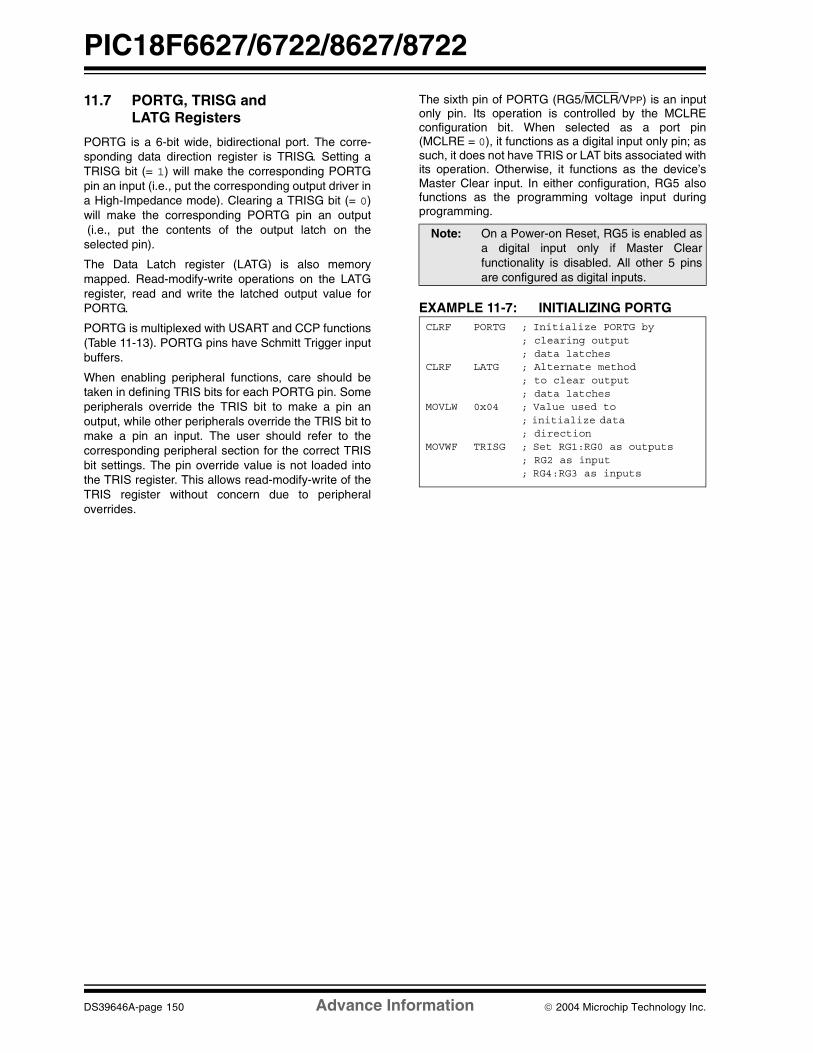
PIC18F6627/6722/8627/8722
DS39646A-page 150 Advance Information 2004 Microchip Technology Inc.
11.7 PORTG, TRISG and LATG Registers
PORTG is a 6-bit wide, bidirectional port. The corre-sponding data direction register is TRISG. Setting aTRISG bit (= 1) will make the corresponding PORTGpin an input (i.e., put the corresponding output driver ina High-Impedance mode). Clearing a TRISG bit (= 0)will make the corresponding PORTG pin an output(i.e., put the contents of the output latch on the
selected pin).
The Data Latch register (LATG) is also memorymapped. Read-modify-write operations on the LATGregister, read and write the latched output value forPORTG.
PORTG is multiplexed with USART and CCP functions(Table 11-13). PORTG pins have Schmitt Trigger inputbuffers.
When enabling peripheral functions, care should betaken in defining TRIS bits for each PORTG pin. Someperipherals override the TRIS bit to make a pin anoutput, while other peripherals override the TRIS bit tomake a pin an input. The user should refer to thecorresponding peripheral section for the correct TRISbit settings. The pin override value is not loaded intothe TRIS register. This allows read-modify-write of theTRIS register without concern due to peripheraloverrides.
The sixth pin of PORTG (RG5/MCLR/VPP) is an inputonly pin. Its operation is controlled by the MCLREconfiguration bit. When selected as a port pin(MCLRE = 0), it functions as a digital input only pin; assuch, it does not have TRIS or LAT bits associated withits operation. Otherwise, it functions as the device’sMaster Clear input. In either configuration, RG5 alsofunctions as the programming voltage input duringprogramming.
EXAMPLE 11-7: INITIALIZING PORTG
Note: On a Power-on Reset, RG5 is enabled asa digital input only if Master Clearfunctionality is disabled. All other 5 pinsare configured as digital inputs.
CLRF PORTG ; Initialize PORTG by; clearing output; data latches
CLRF LATG ; Alternate method; to clear output; data latches
MOVLW 0x04 ; Value used to ; initialize data ; direction
MOVWF TRISG ; Set RG1:RG0 as outputs; RG2 as input; RG4:RG3 as inputs
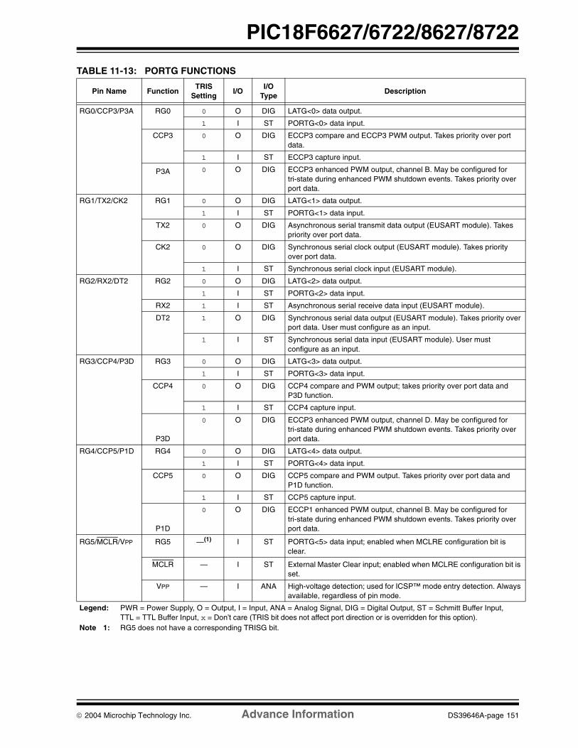
2004 Microchip Technology Inc. Advance Information DS39646A-page 151
PIC18F6627/6722/8627/8722
TABLE 11-13: PORTG FUNCTIONS
Pin Name FunctionTRIS
SettingI/O
I/O Type
Description
RG0/CCP3/P3A RG0 0 O DIG LATG<0> data output.
1 I ST PORTG<0> data input.
CCP3 0 O DIG ECCP3 compare and ECCP3 PWM output. Takes priority over port data.
1 I ST ECCP3 capture input.
P3A 0 O DIG ECCP3 enhanced PWM output, channel B. May be configured for tri-state during enhanced PWM shutdown events. Takes priority over port data.
RG1/TX2/CK2 RG1 0 O DIG LATG<1> data output.
1 I ST PORTG<1> data input.
TX2 0 O DIG Asynchronous serial transmit data output (EUSART module). Takes priority over port data.
CK2 0 O DIG Synchronous serial clock output (EUSART module). Takes priority over port data.
1 I ST Synchronous serial clock input (EUSART module).
RG2/RX2/DT2 RG2 0 O DIG LATG<2> data output.
1 I ST PORTG<2> data input.
RX2 1 I ST Asynchronous serial receive data input (EUSART module).
DT2 1 O DIG Synchronous serial data output (EUSART module). Takes priority over port data. User must configure as an input.
1 I ST Synchronous serial data input (EUSART module). User must configure as an input.
RG3/CCP4/P3D RG3 0 O DIG LATG<3> data output.
1 I ST PORTG<3> data input.
CCP4 0 O DIG CCP4 compare and PWM output; takes priority over port data and P3D function.
1 I ST CCP4 capture input.
P3D
0 O DIG ECCP3 enhanced PWM output, channel D. May be configured for tri-state during enhanced PWM shutdown events. Takes priority over port data.
RG4/CCP5/P1D RG4 0 O DIG LATG<4> data output.
1 I ST PORTG<4> data input.
CCP5 0 O DIG CCP5 compare and PWM output. Takes priority over port data and P1D function.
1 I ST CCP5 capture input.
P1D
0 O DIG ECCP1 enhanced PWM output, channel B. May be configured for tri-state during enhanced PWM shutdown events. Takes priority over port data.
RG5/MCLR/VPP RG5 —(1) I ST PORTG<5> data input; enabled when MCLRE configuration bit is clear.
MCLR — I ST External Master Clear input; enabled when MCLRE configuration bit is set.
VPP — I ANA High-voltage detection; used for ICSP™ mode entry detection. Always available, regardless of pin mode.
Legend: PWR = Power Supply, O = Output, I = Input, ANA = Analog Signal, DIG = Digital Output, ST = Schmitt Buffer Input, TTL = TTL Buffer Input, x = Don’t care (TRIS bit does not affect port direction or is overridden for this option).
Note 1: RG5 does not have a corresponding TRISG bit.

PIC18F6627/6722/8627/8722
DS39646A-page 152 Advance Information 2004 Microchip Technology Inc.
TABLE 11-14: SUMMARY OF REGISTERS ASSOCIATED WITH PORTG
Name Bit 7 Bit 6 Bit 5 Bit 4 Bit 3 Bit 2 Bit 1 Bit 0Reset
Values on Page
PORTG — — RG5(1) Read PORTG pin/Write PORTG Data Latch 60
LATG — — — LATG Data Output Register 60
TRISG — — — Data Direction Control Register for PORTG 60
CCPRxL(2) Capture/Compare/PWM Register x (LSB) 59, 61
CCPRxH(2) Capture/Compare/PWM Register x (MSB) 59, 61
ECCPxCON(2) PxM1 PxM0 DCxB1 DCxB0 CCPxM3 CCPxM2 CCPxM1 CCPxM0 59
ECCPxAS(2) ECCPxASE ECCPxAS2 ECCPxAS1 ECCPxAS0 PSSxAC1 PSSxAC0 PSSxBD1 PSSxBD0 59, 61
ECCPxDEL(2) PxRSEN PxDC6 PxDC5 PxDC4 PxDC3 PxDC2 PxDC1 PxDC0 61
Legend: — = unimplemented, read as ‘0’. Shaded cells are not used by PORTG.Note 1: RG5 is available as an input only when MCLR is disabled.
2: Generic term for all of the identical registers of this name for all enhanced CCP modules, where ‘x’ identifies the individ-ual module (ECCP1, ECCP2 or ECCP3). Bit assignments and Reset values for all registers of the same generic name are identical.
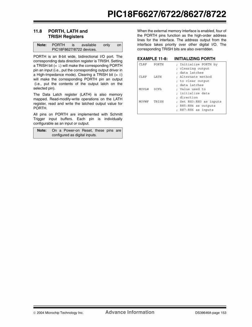
2004 Microchip Technology Inc. Advance Information DS39646A-page 153
PIC18F6627/6722/8627/8722
11.8 PORTH, LATH and TRISH Registers
PORTH is an 8-bit wide, bidirectional I/O port. Thecorresponding data direction register is TRISH. Settinga TRISH bit (= 1) will make the corresponding PORTHpin an input (i.e., put the corresponding output driver ina High-Impedance mode). Clearing a TRISH bit (= 0)will make the corresponding PORTH pin an output(i.e., put the contents of the output latch on the
selected pin).
The Data Latch register (LATH) is also memorymapped. Read-modify-write operations on the LATHregister, read and write the latched output value forPORTH.
All pins on PORTH are implemented with SchmittTrigger input buffers. Each pin is individuallyconfigurable as an input or output.
When the external memory interface is enabled, four ofthe PORTH pins function as the high-order addresslines for the interface. The address output from theinterface takes priority over other digital I/O. Thecorresponding TRISH bits are also overridden.
EXAMPLE 11-8: INITIALIZING PORTH
Note: PORTH is available only onPIC18F8627/8722 devices.
Note: On a Power-on Reset, these pins areconfigured as digital inputs.
CLRF PORTH ; Initialize PORTH by ; clearing output ; data latches
CLRF LATH ; Alternate method ; to clear output ; data latches
MOVLW 0CFh ; Value used to ; initialize data ; direction
MOVWF TRISH ; Set RH3:RH0 as inputs; RH5:RH4 as outputs ; RH7:RH6 as inputs

PIC18F6627/6722/8627/8722
DS39646A-page 154 Advance Information 2004 Microchip Technology Inc.
TABLE 11-15: PORTH FUNCTIONS
Pin Name FunctionTRIS
SettingI/O
I/O Type
Description
RH0/AD16(1) RH0 0 O DIG LATH<0> data output.
1 I ST PORTH<0> data input.
AD16 x O DIG External memory interface, address line 16. Takes priority over port data.
RH1/AD17(1) RH1 0 O DIG LATH<1> data output.
1 I ST PORTH<1> data input.
AD17 x O DIG External memory interface, address line 17. Takes priority over port data.
RH2/AD18(1) RH2 0 O DIG LATH<2> data output.
1 I ST PORTH<2> data input.
AD18 x O DIG External memory interface, address line 18. Takes priority over port data.
RH3/AD19(1) RH3 0 O DIG LATH<3> data output.
1 I ST PORTH<3> data input.
AD19 x O DIG External memory interface, address line 19. Takes priority over port data.
RH4/AN12/P3C(1, 2)
RH4 0 O DIG LATH<4> data output.
1 I ST PORTH<4> data input.
AN12 1 I ANA A/D input channel 12. Default configuration on POR.
P3C 0 O DIG ECCP3 enhanced PWM output, channel C. May be configured for tri-state during enhanced PWM shutdown events. Takes priority over port data.
RH5/AN13/P3B(1, 2)
RH5 0 O DIG LATH<5> data output.
1 I ST PORTH<5> data input.
AN13 1 I ANA A/D input channel 13. Default configuration on POR.
P3B 0 O DIG ECCP3 enhanced PWM output, channel B. May be configured for tri-state during enhanced PWM shutdown events. Takes priority over port data.
RH6/AN14/P1C(1, 2)
RH6 0 O DIG LATH<6> data output.
1 I ST PORTH<6> data input.
AN14 1 I ANA A/D input channel 14. Default configuration on POR.
P1C 0 O DIG ECCP1 enhanced PWM output, channel C. May be configured for tri-state during enhanced PWM shutdown events. Takes priority over port data.
RH7/AN15/P1B(1, 2)
RH7 0 O DIG LATH<7> data output.
1 I ST PORTH<7> data input.
AN15 1 I ANA A/D input channel 15. Default configuration on POR.
P1B 0 O DIG ECCP1 enhanced PWM output, channel B. May be configured for tri-state during enhanced PWM shutdown events. Takes priority over port data.
Legend: PWR = Power Supply, O = Output, I = Input, ANA = Analog Signal, DIG = Digital Output, ST = Schmitt Buffer Input, TTL = TTL Buffer Input, x = Don’t care (TRIS bit does not affect port direction or is overridden for this option).
Note 1: Implemented on 80-pin devices only.2: Alternate assignment for CCP2 when CCP2MX configuration bit is cleared (all devices in Microcontroller mode).

2004 Microchip Technology Inc. Advance Information DS39646A-page 155
PIC18F6627/6722/8627/8722
TABLE 11-16: SUMMARY OF REGISTERS ASSOCIATED WITH PORTH
Name Bit 7 Bit 6 Bit 5 Bit 4 Bit 3 Bit 2 Bit 1 Bit 0Reset Values
on Page
TRISH PORTH Data Direction Control Register 60
PORTH Read PORTH pin/Write PORTH Data Latch 60
LATH Read PORTH Data Latch/Write PORTH Data Latch 60
PIC18F6627/6722/8627/8722
DS39646A-page 156 Advance Information 2004 Microchip Technology Inc.
11.9 PORTJ, TRISJ and LATJ Registers
PORTJ is an 8-bit wide, bidirectional port. The corre-sponding data direction register is TRISJ. Setting aTRISJ bit (= 1) will make the corresponding PORTJ pinan input (i.e., put the corresponding output driver in aHigh-Impedance mode). Clearing a TRISJ bit (= 0) willmake the corresponding PORTJ pin an output (i.e., putthe contents of the output latch on the selected pin).
The Data Latch register (LATJ) is also memorymapped. Read-modify-write operations on the LATJregister, read and write the latched output value forPORTJ.
All pins on PORTJ are implemented with SchmittTrigger input buffers. Each pin is individuallyconfigurable as an input or output.
When the external memory interface is enabled, all ofthe PORTJ pins function as control outputs for theinterface. This occurs automatically when the interfaceis enabled by clearing the EBDIS control bit(MEMCON<7>). The TRISJ bits are also overridden.
EXAMPLE 11-9: INITIALIZING PORTJ
Note: PORTJ is available only onPIC18F8627/8722 devices.
Note: On a Power-on Reset, these pins areconfigured as digital inputs.
CLRF PORTJ ; Initialize PORTJ by; clearing output; data latches
CLRF LATJ ; Alternate method; to clear output; data latches
MOVLW 0xCF ; Value used to ; initialize data ; direction
MOVWF TRISJ ; Set RJ3:RJ0 as inputs; RJ5:RJ4 as output; RJ7:RJ6 as inputs

2004 Microchip Technology Inc. Advance Information DS39646A-page 157
PIC18F6627/6722/8627/8722
TABLE 11-17: PORTJ FUNCTIONS
TABLE 11-18: SUMMARY OF REGISTERS ASSOCIATED WITH PORTJ
Pin Name FunctionTRIS
SettingI/O
I/O Type
Description
RJ0/ALE(1) RJ0 0 O DIG LATJ<0> data output.
1 I ST PORTJ<0> data input.
ALE x O DIG External memory interface address latch enable control output. Takes priority over digital I/O.
RJ1/OE(1) RJ1 0 O DIG LATJ<1> data output.
1 I ST PORTJ<1> data input.
OE x O DIG External memory interface output enable control output. Takes priority over digital I/O.
RJ2/WRL(1) RJ2 0 O DIG LATJ<2> data output.
1 I ST PORTJ<2> data input.
WRL x O DIG External memory bus write low byte control. Takes priority over digital I/O.
RJ3/WRH(1) RJ3 0 O DIG LATJ<3> data output.
1 I ST PORTJ<3> data input.
WRH x O DIG External memory interface write high byte control output. Takes priority over digital I/O.
RJ4/BA0(1) RJ4 0 O DIG LATJ<4> data output.
1 I ST PORTJ<4> data input.
BA0 x O DIG External memory interface byte address 0 control output. Takes prior-ity over digital I/O.
RJ5/CE(1) RJ5 0 O DIG LATJ<5> data output.
1 I ST PORTJ<5> data input.
CE x O DIG External memory interface chip enable control output. Takes priority over digital I/O.
RJ6/LB(1) RJ6 0 O DIG LATJ<6> data output.
1 I ST PORTJ<6> data input.
LB x O DIG External memory interface lower byte enable control output. Takes priority over digital I/O.
RJ7/UB(1) RJ7 0 O DIG LATJ<7> data output.
1 I ST PORTJ<7> data input.
UB x O DIG External memory interface upper byte enable control output. Takes priority over digital I/O.
Legend: PWR = Power Supply, O = Output, I = Input, ANA = Analog Signal, DIG = Digital Output, ST = Schmitt Buffer Input, TTL = TTL Buffer Input, x = Don’t care (TRIS bit does not affect port direction or is overridden for this option).
Note 1: Implemented on 80-pin devices only.
Name Bit 7 Bit 6 Bit 5 Bit 4 Bit 3 Bit 2 Bit 1 Bit 0Reset Values
on Page
PORTJ Read PORTJ pin/Write PORTJ Data Latch 60
LATJ LATJ Data Output Register 60
TRISJ Data Direction Control Register for PORTJ 60
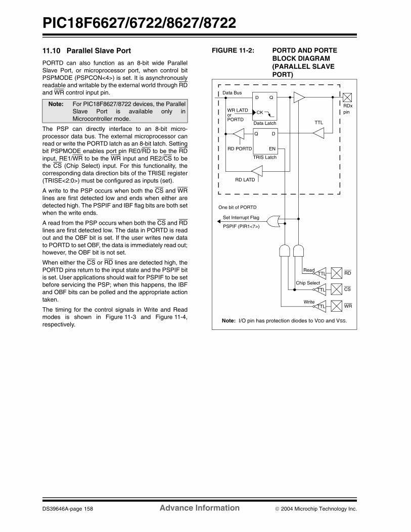
PIC18F6627/6722/8627/8722
DS39646A-page 158 Advance Information 2004 Microchip Technology Inc.
11.10 Parallel Slave Port
PORTD can also function as an 8-bit wide ParallelSlave Port, or microprocessor port, when control bitPSPMODE (PSPCON<4>) is set. It is asynchronouslyreadable and writable by the external world through RDand WR control input pin.
The PSP can directly interface to an 8-bit micro-processor data bus. The external microprocessor canread or write the PORTD latch as an 8-bit latch. Settingbit PSPMODE enables port pin RE0/RD to be the RDinput, RE1/WR to be the WR input and RE2/CS to bethe CS (Chip Select) input. For this functionality, thecorresponding data direction bits of the TRISE register(TRISE<2:0>) must be configured as inputs (set).
A write to the PSP occurs when both the CS and WRlines are first detected low and ends when either aredetected high. The PSPIF and IBF flag bits are both setwhen the write ends.
A read from the PSP occurs when both the CS and RDlines are first detected low. The data in PORTD is readout and the OBF bit is set. If the user writes new datato PORTD to set OBF, the data is immediately read out;however, the OBF bit is not set.
When either the CS or RD lines are detected high, thePORTD pins return to the input state and the PSPIF bitis set. User applications should wait for PSPIF to be setbefore servicing the PSP; when this happens, the IBFand OBF bits can be polled and the appropriate actiontaken.
The timing for the control signals in Write and Readmodes is shown in Figure 11-3 and Figure 11-4,respectively.
FIGURE 11-2: PORTD AND PORTE BLOCK DIAGRAM (PARALLEL SLAVE PORT)
Note: For PIC18F8627/8722 devices, the ParallelSlave Port is available only inMicrocontroller mode.
Data Bus
WR LATDRDx
QD
CK
EN
Q D
ENRD PORTD
pin
One bit of PORTD
Set Interrupt Flag
PSPIF (PIR1<7>)
Read
Chip Select
Write
RD
CS
WR
Note: I/O pin has protection diodes to VDD and VSS.
TTL
TTL
TTL
TTL
orPORTD
RD LATD
Data Latch
TRIS Latch

2004 Microchip Technology Inc. Advance Information DS39646A-page 159
PIC18F6627/6722/8627/8722
REGISTER 11-1: PSPCON: PARALLEL SLAVE PORT CONTROL REGISTER
FIGURE 11-3: PARALLEL SLAVE PORT WRITE WAVEFORMS
R-0 R-0 R/W-0 R/W-0 U-0 U-0 U-0 U-0
IBF OBF IBOV PSPMODE — — — —
bit 7 bit 0
bit 7 IBF: Input Buffer Full Status bit1 = A word has been received and is waiting to be read by the CPU0 = No word has been received
bit 6 OBF: Output Buffer Full Status bit
1 = The output buffer still holds a previously written word0 = The output buffer has been read
bit 5 IBOV: Input Buffer Overflow Detect bit1 = A write occurred when a previously input word has not been read
(must be cleared in software)0 = No overflow occurred
bit 4 PSPMODE: Parallel Slave Port Mode Select bit
1 = Parallel Slave Port mode0 = General Purpose I/O mode
bit 3-0 Unimplemented: Read as ‘0’
Legend:
R = Readable bit W = Writable bit U = Unimplemented bit, read as ‘0’
-n = Value at POR ‘1’ = Bit is set ‘0’ = Bit is cleared x = Bit is unknown
Q1 Q2 Q3 Q4
CS
Q1 Q2 Q3 Q4 Q1 Q2 Q3 Q4
WR
RD
IBF
OBF
PSPIF
PORTD<7:0>

PIC18F6627/6722/8627/8722
DS39646A-page 160 Advance Information 2004 Microchip Technology Inc.
FIGURE 11-4: PARALLEL SLAVE PORT READ WAVEFORMS
TABLE 11-19: REGISTERS ASSOCIATED WITH PARALLEL SLAVE PORT
Q1 Q2 Q3 Q4
CS
Q1 Q2 Q3 Q4 Q1 Q2 Q3 Q4
WR
IBF
PSPIF
RD
OBF
PORTD<7:0>
Name Bit 7 Bit 6 Bit 5 Bit 4 Bit 3 Bit 2 Bit 1 Bit 0Reset Values
on Page
PORTD PORTD Data Latch when written; PORTD pins when read 60
LATD LATD Data Output bits 60
TRISD PORTD Data Direction bits 60
PORTE PORTE Data Latch when written; PORTE pins when read 60
LATE LATE Data Output bits 60
TRISE PORTE Data Direction bits 60
PSPCON IBF OBF IBOV PSPMODE — — — — 59
INTCON GIE/GIEH PEIE/GIEL TMR0IE INT0IE RBIE TMR0IF INT0IF RBIF 57
PIR1 PSPIF ADIF RC1IF TX1IF SSP1IF CCP1IF TMR2IF TMR1IF 60
PIE1 PSPIE ADIE RC1IE TX1IE SSP1IE CCP1IE TMR2IE TMR1IE 60
IPR1 PSPIP ADIP RC1IP TX1IP SSP1IP CCP1IP TMR2IP TMR1IP 60
Legend: — = unimplemented, read as ‘0’. Shaded cells are not used by the Parallel Slave Port.

2004 Microchip Technology Inc. Advance Information DS39646A-page 161
PIC18F6627/6722/8627/8722
12.0 TIMER0 MODULE
The Timer0 module incorporates the following features:
• Software selectable operation as a timer or counter in both 8-bit or 16-bit modes
• Readable and writable registers• Dedicated 8-bit, software programmable
prescaler• Selectable clock source (internal or external)• Edge select for external clock
• Interrupt-on-overflow
The T0CON register (Register 12-1) controls allaspects of the module’s operation, including theprescale selection. It is both readable and writable.
A simplified block diagram of the Timer0 module in 8-bitmode is shown in Figure 12-1. Figure 12-2 shows asimplified block diagram of the Timer0 module in 16-bitmode.
REGISTER 12-1: T0CON: TIMER0 CONTROL REGISTER R/W-1 R/W-1 R/W-1 R/W-1 R/W-1 R/W-1 R/W-1 R/W-1
TMR0ON T08BIT T0CS T0SE PSA T0PS2 T0PS1 T0PS0
bit 7 bit 0
bit 7 TMR0ON: Timer0 On/Off Control bit 1 = Enables Timer0 0 = Stops Timer0
bit 6 T08BIT: Timer0 8-bit/16-bit Control bit
1 = Timer0 is configured as an 8-bit timer/counter 0 = Timer0 is configured as a 16-bit timer/counter
bit 5 T0CS: Timer0 Clock Source Select bit 1 = Transition on T0CKI pin 0 = Internal instruction cycle clock (CLKO)
bit 4 T0SE: Timer0 Source Edge Select bit1 = Increment on high-to-low transition on T0CKI pin 0 = Increment on low-to-high transition on T0CKI pin
bit 3 PSA: Timer0 Prescaler Assignment bit
1 = TImer0 prescaler is NOT assigned. Timer0 clock input bypasses prescaler. 0 = Timer0 prescaler is assigned. Timer0 clock input comes from prescaler output.
bit 2-0 T0PS2:T0PS0: Timer0 Prescaler Select bits 111 = 1:256 prescale value110 = 1:128 prescale value101 = 1:64 prescale value100 = 1:32 prescale value011 = 1:16 prescale value010 = 1:8 prescale value001 = 1:4 prescale value000 = 1:2 prescale value
Legend:
R = Readable bit W = Writable bit U = Unimplemented bit, read as ‘0’
-n = Value at POR ‘1’ = Bit is set ‘0’ = Bit is cleared x = Bit is unknown
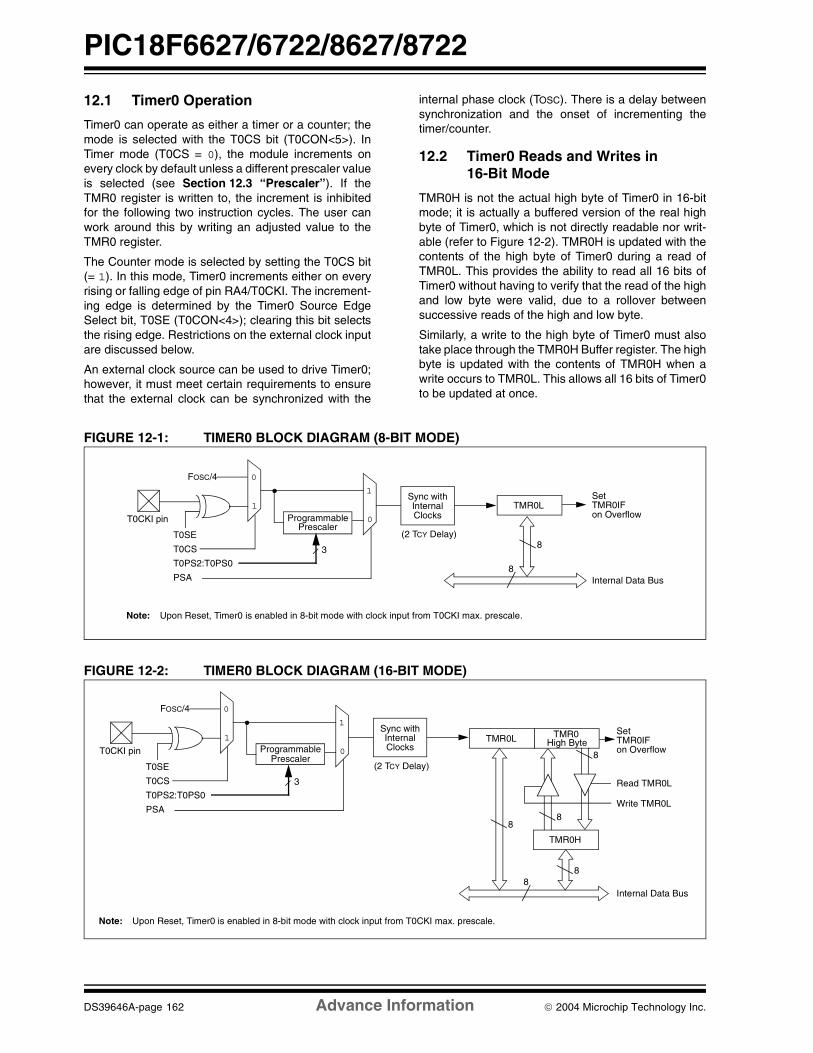
PIC18F6627/6722/8627/8722
DS39646A-page 162 Advance Information 2004 Microchip Technology Inc.
12.1 Timer0 Operation
Timer0 can operate as either a timer or a counter; themode is selected with the T0CS bit (T0CON<5>). InTimer mode (T0CS = 0), the module increments onevery clock by default unless a different prescaler valueis selected (see Section 12.3 “Prescaler”). If theTMR0 register is written to, the increment is inhibitedfor the following two instruction cycles. The user canwork around this by writing an adjusted value to theTMR0 register.
The Counter mode is selected by setting the T0CS bit(= 1). In this mode, Timer0 increments either on everyrising or falling edge of pin RA4/T0CKI. The increment-ing edge is determined by the Timer0 Source EdgeSelect bit, T0SE (T0CON<4>); clearing this bit selectsthe rising edge. Restrictions on the external clock inputare discussed below.
An external clock source can be used to drive Timer0;however, it must meet certain requirements to ensurethat the external clock can be synchronized with the
internal phase clock (TOSC). There is a delay betweensynchronization and the onset of incrementing thetimer/counter.
12.2 Timer0 Reads and Writes in 16-Bit Mode
TMR0H is not the actual high byte of Timer0 in 16-bitmode; it is actually a buffered version of the real highbyte of Timer0, which is not directly readable nor writ-able (refer to Figure 12-2). TMR0H is updated with thecontents of the high byte of Timer0 during a read ofTMR0L. This provides the ability to read all 16 bits ofTimer0 without having to verify that the read of the highand low byte were valid, due to a rollover betweensuccessive reads of the high and low byte.
Similarly, a write to the high byte of Timer0 must alsotake place through the TMR0H Buffer register. The highbyte is updated with the contents of TMR0H when awrite occurs to TMR0L. This allows all 16 bits of Timer0to be updated at once.
FIGURE 12-1: TIMER0 BLOCK DIAGRAM (8-BIT MODE)
FIGURE 12-2: TIMER0 BLOCK DIAGRAM (16-BIT MODE)
Note: Upon Reset, Timer0 is enabled in 8-bit mode with clock input from T0CKI max. prescale.
T0CKI pin
T0SE
0
1
1
0
T0CS
FOSC/4
ProgrammablePrescaler
Sync withInternalClocks
TMR0L
(2 TCY Delay)
Internal Data BusPSA
T0PS2:T0PS0
Set TMR0IFon Overflow
3 8
8
Note: Upon Reset, Timer0 is enabled in 8-bit mode with clock input from T0CKI max. prescale.
T0CKI pin
T0SE
0
1
1
0
T0CS
FOSC/4
ProgrammablePrescaler
Sync withInternalClocks
TMR0L
(2 TCY Delay)
Internal Data Bus
8
PSA
T0PS2:T0PS0
Set TMR0IFon Overflow
3
TMR0
TMR0H
High Byte
88
8
Read TMR0L
Write TMR0L
8

2004 Microchip Technology Inc. Advance Information DS39646A-page 163
PIC18F6627/6722/8627/8722
12.3 Prescaler
An 8-bit counter is available as a prescaler for the Timer0module. The prescaler is not directly readable or writable;its value is set by the PSA and T0PS2:T0PS0 bits(T0CON<3:0>) which determine the prescalerassignment and prescale ratio.
Clearing the PSA bit assigns the prescaler to theTimer0 module. When it is assigned, prescale valuesfrom 1:2 through 1:256 in power-of-2 increments areselectable.
When assigned to the Timer0 module, all instructionswriting to the TMR0 register (e.g., CLRF TMR0, MOVWFTMR0, BSF TMR0, etc.) clear the prescaler count.
12.3.1 SWITCHING PRESCALER ASSIGNMENT
The prescaler assignment is fully under softwarecontrol and can be changed “on-the-fly” during programexecution.
12.4 Timer0 Interrupt
The TMR0 interrupt is generated when the TMR0register overflows from FFh to 00h in 8-bit mode, orfrom FFFFh to 0000h in 16-bit mode. This overflow setsthe TMR0IF flag bit. The interrupt can be masked byclearing the TMR0IE bit (INTCON<5>). Before re-enabling the interrupt, the TMR0IF bit must be clearedin software by the Interrupt Service Routine.
Since Timer0 is shut down in Sleep mode, the TMR0interrupt cannot awaken the processor from Sleep.
TABLE 12-1: REGISTERS ASSOCIATED WITH TIMER0
Note: Writing to TMR0 when the prescaler isassigned to Timer0 will clear the prescalercount, but will not change the prescalerassignment.
Name Bit 7 Bit 6 Bit 5 Bit 4 Bit 3 Bit 2 Bit 1 Bit 0Reset Values
on page
TMR0L Timer0 Register, Low Byte 58
TMR0H Timer0 Register, High Byte 58
INTCON GIE/GIEH PEIE/GIEL TMR0IE INT0IE RBIE TMR0IF INT0IF RBIF 57
T0CON TMR0ON T08BIT T0CS T0SE PSA T0PS2 T0PS1 T0PS0 58
TRISA TRISA7(1) TRISA6(1) Data Direction Control Register for PORTA 60
Legend: Shaded cells are not used by Timer0.Note 1: PORTA<7:6> and their direction bits are individually configured as port pins based on various primary
oscillator modes. When disabled, these bits read as ‘0’.

PIC18F6627/6722/8627/8722
DS39646A-page 164 Advance Information 2004 Microchip Technology Inc.
NOTES:

2004 Microchip Technology Inc. Advance Information DS39646A-page 165
PIC18F6627/6722/8627/8722
13.0 TIMER1 MODULE
The Timer1 timer/counter module incorporates thesefeatures:
• Software selectable operation as a 16-bit timer or counter
• Readable and writable 8-bit registers (TMR1H and TMR1L)
• Selectable clock source (internal or external) with device clock or Timer1 oscillator internal options
• Interrupt-on-overflow
• Reset on CCP special event trigger• Device clock status flag (T1RUN)
A simplified block diagram of the Timer1 module isshown in Figure 13-1. A block diagram of the module’soperation in Read/Write mode is shown in Figure 13-2.
The module incorporates its own low-power oscillatorto provide an additional clocking option. The Timer1oscillator can also be used as a low-power clock sourcefor the microcontroller in power-managed operation.
Timer1 can also be used to provide Real-Time Clock(RTC) functionality to applications with only a minimaladdition of external components and code overhead.
Timer1 is controlled through the T1CON Controlregister (Register 13-1). It also contains the Timer1Oscillator Enable bit (T1OSCEN). Timer1 can beenabled or disabled by setting or clearing control bit,TMR1ON (T1CON<0>).
REGISTER 13-1: T1CON: TIMER1 CONTROL REGISTER R/W-0 R-0 R/W-0 R/W-0 R/W-0 R/W-0 R/W-0 R/W-0
RD16 T1RUN T1CKPS1 T1CKPS0 T1OSCEN T1SYNC TMR1CS TMR1ON
bit 7 bit 0
bit 7 RD16: 16-bit Read/Write Mode Enable bit
1 = Enables register read/write of TImer1 in one 16-bit operation0 = Enables register read/write of Timer1 in two 8-bit operations
bit 6 T1RUN: Timer1 System Clock Status bit1 = Device clock is derived from Timer1 oscillator0 = Device clock is derived from another source
bit 5-4 T1CKPS1:T1CKPS0: Timer1 Input Clock Prescale Select bits11 = 1:8 Prescale value 10 = 1:4 Prescale value 01 = 1:2 Prescale value 00 = 1:1 Prescale value
bit 3 T1OSCEN: Timer1 Oscillator Enable bit1 = Timer1 oscillator is enabled 0 = Timer1 oscillator is shut off The oscillator inverter and feedback resistor are turned off to eliminate power drain.
bit 2 T1SYNC: Timer1 External Clock Input Synchronization Select bitWhen TMR1CS = 1: 1 = Do not synchronize external clock input 0 = Synchronize external clock inputWhen TMR1CS = 0: This bit is ignored. Timer1 uses the internal clock when TMR1CS = 0.
bit 1 TMR1CS: Timer1 Clock Source Select bit
1 = External clock from pin RC0/T1OSO/T13CKI (on the rising edge) 0 = Internal clock (FOSC/4)
bit 0 TMR1ON: Timer1 On bit1 = Enables Timer1 0 = Stops Timer1
Legend:R = Readable bit W = Writable bit U = Unimplemented bit, read as ‘0’-n = Value at POR ‘1’ = Bit is set ‘0’ = Bit is cleared x = Bit is unknown

PIC18F6627/6722/8627/8722
DS39646A-page 166 Advance Information 2004 Microchip Technology Inc.
13.1 Timer1 Operation
Timer1 can operate in one of these modes:
• Timer
• Synchronous Counter• Asynchronous Counter
The operating mode is determined by the clock selectbit, TMR1CS (T1CON<1>). When TMR1CS is cleared(= 0), Timer1 increments on every internal instruction
cycle (Fosc/4). When the bit is set, Timer1 incrementson every rising edge of the Timer1 external clock inputor the Timer1 oscillator, if enabled.
When Timer1 is enabled, the RC1/T1OSI and RC0/T1OSO/T13CKI pins become inputs. This means thevalues of TRISC<1:0> are ignored and the pins areread as ‘0’.
FIGURE 13-1: TIMER1 BLOCK DIAGRAM
FIGURE 13-2: TIMER1 BLOCK DIAGRAM (16-BIT READ/WRITE MODE)
T1SYNC
TMR1CS
T1CKPS1:T1CKPS0
Sleep InputT1OSCEN(1)
FOSC/4InternalClock
On/Off
Prescaler1, 2, 4, 8
Synchronize
Detect
1
0
2
T1OSO/T13CKI
T1OSI
1
0
TMR1ON
TMR1LSet
TMR1IFon Overflow
TMR1 High ByteClear TMR1
(CCP special event trigger)
Timer1 Oscillator
Note 1: When enable bit, T1OSCEN, is cleared, the inverter and feedback resistor are turned off to eliminate power drain.
On/OffTimer1
Timer1 Clock Input
T1SYNC
TMR1CS
T1CKPS1:T1CKPS0
Sleep InputT1OSCEN(1)
FOSC/4InternalClock
Prescaler1, 2, 4, 8
Synchronize
Detect
1
0
2
T1OSO/T13CKI
T1OSI
Note 1: When enable bit, T1OSCEN, is cleared, the inverter and feedback resistor are turned off to eliminate power drain.
1
0
TMR1L
Internal Data Bus
8
Set TMR1IF
on Overflow
TMR1
TMR1H
High Byte
88
8
Read TMR1L
Write TMR1L
8
TMR1ON
Clear TMR1(CCP special event trigger)
Timer1 Oscillator
On/OffTimer1
Timer1 Clock Input

2004 Microchip Technology Inc. Advance Information DS39646A-page 167
PIC18F6627/6722/8627/8722
13.2 Timer1 16-Bit Read/Write Mode
Timer1 can be configured for 16-bit reads and writes(see Figure 13-2). When the RD16 control bit(T1CON<7>) is set, the address for TMR1H is mappedto a buffer register for the high byte of Timer1. A readfrom TMR1L will load the contents of the high byte ofTimer1 into the Timer1 high byte buffer. This providesthe user with the ability to accurately read all 16 bits ofTimer1 without having to determine whether a read ofthe high byte, followed by a read of the low byte, hasbecome invalid due to a rollover between reads.
A write to the high byte of Timer1 must also take placethrough the TMR1H Buffer register. The Timer1 highbyte is updated with the contents of TMR1H when awrite occurs to TMR1L. This allows a user to write all16 bits to both the high and low bytes of Timer1 at once.
The high byte of Timer1 is not directly readable orwritable in this mode. All reads and writes must takeplace through the Timer1 High Byte Buffer register.Writes to TMR1H do not clear the Timer1 prescaler.The prescaler is only cleared on writes to TMR1L.
13.3 Timer1 Oscillator
An on-chip crystal oscillator circuit is incorporatedbetween pins T1OSI (input) and T1OSO (amplifier out-put). It is enabled by setting the Timer1 Oscillator Enablebit, T1OSCEN (T1CON<3>). The oscillator is a low-power circuit rated for 32 kHz crystals. It will continue torun during all power-managed modes. The circuit for atypical LP oscillator is shown in Figure 13-3. Table 13-1shows the capacitor selection for the Timer1 oscillator.
The user must provide a software time delay to ensureproper start-up of the Timer1 oscillator.
FIGURE 13-3: EXTERNAL COMPONENTS FOR THE TIMER1 LP OSCILLATOR
TABLE 13-1: CAPACITOR SELECTION FOR THE TIMER OSCILLATOR(2,3,4)
13.3.1 USING TIMER1 AS A CLOCK SOURCE
The Timer1 oscillator is also available as a clock sourcein power-managed modes. By setting the clock selectbits, SCS1:SCS0 (OSCCON<1:0>), to ‘01’, the deviceswitches to SEC_RUN mode; both the CPU andperipherals are clocked from the Timer1 oscillator. If theIDLEN bit (OSCCON<7>) is cleared and a SLEEPinstruction is executed, the device enters SEC_IDLEmode. Additional details are available in Section 3.0“Power-Managed Modes”.
Whenever the Timer1 oscillator is providing the clocksource, the Timer1 system clock status flag, T1RUN(T1CON<6>), is set. This can be used to determine thecontroller’s current clocking mode. It can also indicatethe clock source being currently used by the Fail-SafeClock Monitor. If the Clock Monitor is enabled and theTimer1 oscillator fails while providing the clock, pollingthe T1RUN bit will indicate whether the clock is beingprovided by the Timer1 oscillator or another source.
13.3.2 LOW-POWER TIMER1 OPTION
The Timer1 oscillator can operate at two distinct levelsof power consumption based on device configuration.When the LPT1OSC configuration bit is set, the Timer1oscillator operates in a low-power mode. WhenLPT1OSC is not set, Timer1 operates at a higher powerlevel. Power consumption for a particular mode is rela-tively constant, regardless of the device’s operatingmode. The default Timer1 configuration is the higherpower mode.
As the low-power Timer1 mode tends to be more sen-sitive to interference, high noise environments maycause some oscillator instability. The low-power optionis, therefore, best suited for low noise applicationswhere power conservation is an important designconsideration.
Note: See the Notes with Table 13-1 for additionalinformation about capacitor selection.
C1
C2
XTAL
PIC18FXXXX
T1OSI
T1OSO
32.768 kHz
27 pF
27 pF
Osc Type Freq C1 C2
LP 32 kHz 27 pF(1) 27 pF(1)
Note 1: Microchip suggests these values as astarting point in validating the oscillatorcircuit.
2: Higher capacitance increases the stabilityof the oscillator but also increases thestart-up time.
3: Since each resonator/crystal has its owncharacteristics, the user should consultthe resonator/crystal manufacturer forappropriate values of externalcomponents.
4: Capacitor values are for design guidanceonly.

PIC18F6627/6722/8627/8722
DS39646A-page 168 Advance Information 2004 Microchip Technology Inc.
13.3.3 TIMER1 OSCILLATOR LAYOUT CONSIDERATIONS
The Timer1 oscillator circuit draws very little powerduring operation. Due to the low-power nature of theoscillator, it may also be sensitive to rapidly changingsignals in close proximity.
The oscillator circuit, shown in Figure 13-3, should belocated as close as possible to the microcontroller.There should be no circuits passing within the oscillatorcircuit boundaries other than VSS or VDD.
If a high-speed circuit must be located near the Timer1oscillator, a grounded guard ring around the oscillatorcircuit may be helpful when used on a single-sidedPCB or in addition to a ground plane.
13.4 Timer1 Interrupt
The TMR1 register pair (TMR1H:TMR1L) incrementsfrom 0000h to FFFFh and rolls over to 0000h. TheTimer1 interrupt, if enabled, is generated on overflow,which is latched in interrupt flag bit, TMR1IF(PIR1<0>). This interrupt can be enabled or disabledby setting or clearing the Timer1 Interrupt Enable bit,TMR1IE (PIE1<0>).
13.5 Resetting Timer1 Using the CCP Special Event Trigger
If any of the CCP modules are configured to use Timer1and generate a special event trigger in Compare mode(CCPxM3:CCPxM0, this signal will reset Timer1. Thetrigger from the ECCP2 module will also start an A/Dconversion if the A/D module is enabled (seeSection 17.3.4 “Special Event Trigger” for more infor-mation).
The module must be configured as either a timer or asynchronous counter to take advantage of this feature.When used this way, the CCPRH:CCPRL register paireffectively becomes a period register for Timer1.
If Timer1 is running in Asynchronous Counter mode,this Reset operation may not work.
In the event that a write to Timer1 coincides with aspecial event trigger, the write operation will takeprecedence.
13.6 Using Timer1 as a Real-Time Clock
Adding an external LP oscillator to Timer1 (such as theone described in Section 13.3 “Timer1 Oscillator”above) gives users the option to include RTC function-ality to their applications. This is accomplished with aninexpensive watch crystal to provide an accurate timebase and several lines of application code to calculatethe time. When operating in Sleep mode and using abattery or supercapacitor as a power source, it cancompletely eliminate the need for a separate RTCdevice and battery backup.
The application code routine, RTCisr, shown inExample 13-1, demonstrates a simple method toincrement a counter at one-second intervals using anInterrupt Service Routine. Incrementing the TMR1 reg-ister pair to overflow triggers the interrupt and calls theroutine, which increments the seconds counter by one;additional counters for minutes and hours areincremented as the previous counter overflow.
Since the register pair is 16 bits wide, counting up tooverflow the register directly from a 32.768 kHz clockwould take 2 seconds. To force the overflow at therequired one-second intervals, it is necessary to pre-load it; the simplest method is to set the MSb of TMR1Hwith a BSF instruction. Note that the TMR1L register isnever preloaded or altered; doing so may introducecumulative error over many cycles.
For this method to be accurate, Timer1 must operate inAsynchronous mode and the Timer1 overflow interruptmust be enabled (PIE1<0> = 1), as shown in theroutine, RTCinit. The Timer1 oscillator must also beenabled and running at all times.
Note: The special event triggers from the CCPxmodule will not set the TMR1IF interruptflag bit (PIR1<0>).

2004 Microchip Technology Inc. Advance Information DS39646A-page 169
PIC18F6627/6722/8627/8722
EXAMPLE 13-1: IMPLEMENTING A REAL-TIME CLOCK USING A TIMER1 INTERRUPT SERVICE
TABLE 13-2: REGISTERS ASSOCIATED WITH TIMER1 AS A TIMER/COUNTER
RTCinitMOVLW 80h ; Preload TMR1 register pairMOVWF TMR1H ; for 1 second overflowCLRF TMR1LMOVLW b’00001111’ ; Configure for external clock,MOVWF T1CON ; Asynchronous operation, external oscillatorCLRF secs ; Initialize timekeeping registersCLRF mins ; MOVLW .12MOVWF hoursBSF PIE1, TMR1IE ; Enable Timer1 interruptRETURN
RTCisrBSF TMR1H, 7 ; Preload for 1 sec overflowBCF PIR1, TMR1IF ; Clear interrupt flagINCF secs, F ; Increment secondsMOVLW .59 ; 60 seconds elapsed?CPFSGT secsRETURN ; No, doneCLRF secs ; Clear secondsINCF mins, F ; Increment minutesMOVLW .59 ; 60 minutes elapsed?CPFSGT minsRETURN ; No, doneCLRF mins ; clear minutesINCF hours, F ; Increment hoursMOVLW .23 ; 24 hours elapsed?CPFSGT hoursRETURN ; No, doneCLRF hours ; Reset hoursRETURN ; Done
Name Bit 7 Bit 6 Bit 5 Bit 4 Bit 3 Bit 2 Bit 1 Bit 0Reset Values
on page
INTCON GIE/GIEH PEIE/GIEL TMR0IE INT0IE RBIE TMR0IF INT0IF RBIF 57
PIR1 PSPIF ADIF RC1IF TX1IF SSP1IF CCP1IF TMR2IF TMR1IF 60
PIE1 PSPIE ADIE RC1IE TX1IE SSP1IE CCP1IE TMR2IE TMR1IE 60
IPR1 PSPIP ADIP RC1IP TX1IP SSP1IP CCP1IP TMR2IP TMR1IP 60
TMR1L Timer1 Register, Low Byte 58
TMR1H Timer1 Register, High Byte 58
T1CON RD16 T1RUN T1CKPS1 T1CKPS0 T1OSCEN T1SYNC TMR1CS TMR1ON 58
Legend: Shaded cells are not used by the Timer1 module.

PIC18F6627/6722/8627/8722
DS39646A-page 170 Advance Information 2004 Microchip Technology Inc.
NOTES:
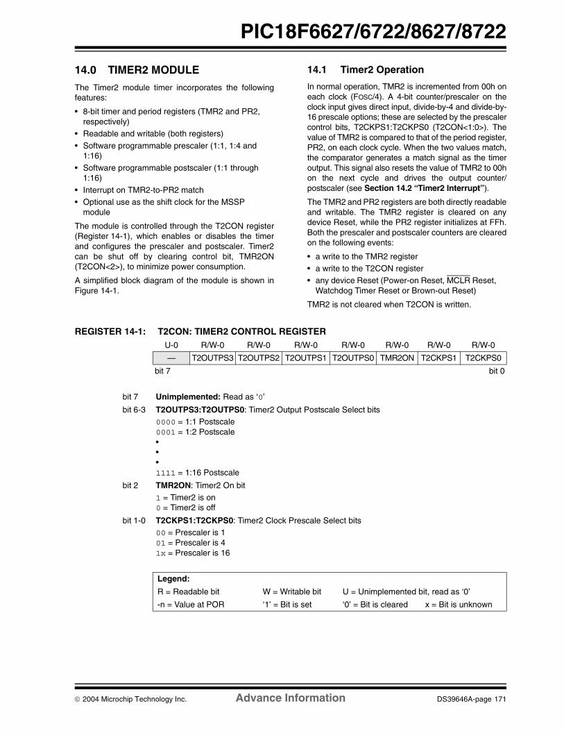
2004 Microchip Technology Inc. Advance Information DS39646A-page 171
PIC18F6627/6722/8627/8722
14.0 TIMER2 MODULE
The Timer2 module timer incorporates the followingfeatures:
• 8-bit timer and period registers (TMR2 and PR2, respectively)
• Readable and writable (both registers)
• Software programmable prescaler (1:1, 1:4 and 1:16)
• Software programmable postscaler (1:1 through 1:16)
• Interrupt on TMR2-to-PR2 match• Optional use as the shift clock for the MSSP
module
The module is controlled through the T2CON register(Register 14-1), which enables or disables the timerand configures the prescaler and postscaler. Timer2can be shut off by clearing control bit, TMR2ON(T2CON<2>), to minimize power consumption.
A simplified block diagram of the module is shown inFigure 14-1.
14.1 Timer2 Operation
In normal operation, TMR2 is incremented from 00h oneach clock (FOSC/4). A 4-bit counter/prescaler on theclock input gives direct input, divide-by-4 and divide-by-16 prescale options; these are selected by the prescalercontrol bits, T2CKPS1:T2CKPS0 (T2CON<1:0>). Thevalue of TMR2 is compared to that of the period register,PR2, on each clock cycle. When the two values match,the comparator generates a match signal as the timeroutput. This signal also resets the value of TMR2 to 00hon the next cycle and drives the output counter/postscaler (see Section 14.2 “Timer2 Interrupt”).
The TMR2 and PR2 registers are both directly readableand writable. The TMR2 register is cleared on anydevice Reset, while the PR2 register initializes at FFh.Both the prescaler and postscaler counters are clearedon the following events:
• a write to the TMR2 register• a write to the T2CON register• any device Reset (Power-on Reset, MCLR Reset,
Watchdog Timer Reset or Brown-out Reset)
TMR2 is not cleared when T2CON is written.
REGISTER 14-1: T2CON: TIMER2 CONTROL REGISTER U-0 R/W-0 R/W-0 R/W-0 R/W-0 R/W-0 R/W-0 R/W-0
— T2OUTPS3 T2OUTPS2 T2OUTPS1 T2OUTPS0 TMR2ON T2CKPS1 T2CKPS0
bit 7 bit 0
bit 7 Unimplemented: Read as ‘0’
bit 6-3 T2OUTPS3:T2OUTPS0: Timer2 Output Postscale Select bits0000 = 1:1 Postscale 0001 = 1:2 Postscale • • • 1111 = 1:16 Postscale
bit 2 TMR2ON: Timer2 On bit
1 = Timer2 is on 0 = Timer2 is off
bit 1-0 T2CKPS1:T2CKPS0: Timer2 Clock Prescale Select bits00 = Prescaler is 1 01 = Prescaler is 4 1x = Prescaler is 16
Legend:
R = Readable bit W = Writable bit U = Unimplemented bit, read as ‘0’
-n = Value at POR ‘1’ = Bit is set ‘0’ = Bit is cleared x = Bit is unknown

PIC18F6627/6722/8627/8722
DS39646A-page 172 Advance Information 2004 Microchip Technology Inc.
14.2 Timer2 Interrupt
Timer2 also can generate an optional device interrupt.The Timer2 output signal (TMR2-to-PR2 match) pro-vides the input for the 4-bit output counter/postscaler.This counter generates the TMR2 match interrupt flagwhich is latched in TMR2IF (PIR1<1>). The interrupt isenabled by setting the TMR2 Match Interrupt Enablebit, TMR2IE (PIE1<1>).
A range of 16 postscale options (from 1:1 through 1:16inclusive) can be selected with the postscaler controlbits, T2OUTPS3:T2OUTPS0 (T2CON<6:3>).
14.3 Timer2 Output
The unscaled output of TMR2 is available primarily tothe CCP modules, where it is used as a time base foroperations in PWM mode.
Timer2 can be optionally used as the shift clock sourcefor the MSSP module operating in SPI mode. Addi-tional information is provided in Section 19.0 “MasterSynchronous Serial Port (MSSP) Module”.
FIGURE 14-1: TIMER2 BLOCK DIAGRAM
TABLE 14-1: REGISTERS ASSOCIATED WITH TIMER2 AS A TIMER/COUNTER
Name Bit 7 Bit 6 Bit 5 Bit 4 Bit 3 Bit 2 Bit 1 Bit 0Reset Values
on page
INTCON GIE/GIEH PEIE/GIEL TMR0IE INT0IE RBIE TMR0IF INT0IF RBIF 57
PIR1 PSPIF ADIF RC1IF TX1IF SSP1IF CCP1IF TMR2IF TMR1IF 60
PIE1 PSPIE ADIE RC1IE TX1IE SSP1IE CCP1IE TMR2IE TMR1IE 60
IPR1 PSPIP ADIP RC1IP TX1IP SSP1IP CCP1IP TMR2IP TMR1IP 60
TMR2 Timer2 Register 58
T2CON — T2OUTPS3 T2OUTPS2 T2OUTPS1 T2OUTPS0 TMR2ON T2CKPS1 T2CKPS0 58
PR2 Timer2 Period Register 58
Legend: — = unimplemented, read as ‘0’. Shaded cells are not used by the Timer2 module.
Comparator
TMR2 Output
TMR2
Postscaler
PrescalerPR2
2
FOSC/4
1:1 to 1:16
1:1, 1:4, 1:16
4T2OUTPS3:T2OUTPS0
T2CKPS1:T2CKPS0
Set TMR2IF
Internal Data Bus8
ResetTMR2/PR2
88
(to PWM or MSSP)
Match

2004 Microchip Technology Inc. Advance Information DS39646A-page 173
PIC18F6627/6722/8627/8722
15.0 TIMER3 MODULE
The Timer3 module timer/counter incorporates thesefeatures:
• Software selectable operation as a 16-bit timer or counter
• Readable and writable 8-bit registers (TMR3H and TMR3L)
• Selectable clock source (internal or external) with device clock or Timer1 oscillator internal options
• Interrupt-on-overflow
• Module Reset on CCP special event trigger
A simplified block diagram of the Timer3 module isshown in Figure 15-1. A block diagram of the module’soperation in Read/Write mode is shown in Figure 15-2.
The Timer3 module is controlled through the T3CONregister (Register 15-1). It also selects the clock sourceoptions for the CCP modules (see Section 17.1.1“CCP Modules and Timer Resources” for moreinformation).
REGISTER 15-1: T3CON: TIMER3 CONTROL REGISTER R/W-0 R/W-0 R/W-0 R/W-0 R/W-0 R/W-0 R/W-0 R/W-0
RD16 T3CCP2 T3CKPS1 T3CKPS0 T3CCP1 T3SYNC TMR3CS TMR3ON
bit 7 bit 0
bit 7 RD16: 16-bit Read/Write Mode Enable bit1 = Enables register read/write of Timer3 in one 16-bit operation0 = Enables register read/write of Timer3 in two 8-bit operations
bit 6,3 T3CCP2:T3CCP1: Timer3 and Timer1 to CCPx Enable bits
11 =Timer3 and Timer4 are the clock sources for CCP1 through CCP510 =Timer3 and Timer4 are the clock sources for CCP3 through CCP5;
Timer1 and Timer2 are the clock sources for CCP1 and CCP201 =Timer3 and Timer4 are the clock sources for CCP2 through CCP5;
Timer1 and Timer2 are the clock sources for CCP100 =Timer1 and Timer2 are the clock sources for CCP1 through CCP5
bit 5-4 T3CKPS1:T3CKPS0: Timer3 Input Clock Prescale Select bits
11 = 1:8 Prescale value10 = 1:4 Prescale value01 = 1:2 Prescale value00 = 1:1 Prescale value
bit 2 T3SYNC: Timer3 External Clock Input Synchronization Control bit (Not usable if the device clock comes from Timer1/Timer3.)When TMR3CS = 1:1 = Do not synchronize external clock input0 = Synchronize external clock inputWhen TMR3CS = 0:This bit is ignored. Timer3 uses the internal clock when TMR3CS = 0.
bit 1 TMR3CS: Timer3 Clock Source Select bit
1 = External clock input from Timer1 oscillator or T13CKI (on the rising edge after the first falling edge)
0 = Internal clock (FOSC/4)
bit 0 TMR3ON: Timer3 On bit1 = Enables Timer3 0 = Stops Timer3
Legend:
R = Readable bit W = Writable bit U = Unimplemented bit, read as ‘0’
-n = Value at POR ‘1’ = Bit is set ‘0’ = Bit is cleared x = Bit is unknown

PIC18F6627/6722/8627/8722
DS39646A-page 174 Advance Information 2004 Microchip Technology Inc.
15.1 Timer3 Operation
Timer3 can operate in one of three modes:
• Timer
• Synchronous Counter• Asynchronous Counter
The operating mode is determined by the clock selectbit, TMR3CS (T3CON<1>). When TMR3CS is cleared(= 0), Timer3 increments on every internal instructioncycle (FOSC/4). When the bit is set, Timer3 incrementson every rising edge of the Timer1 external clock inputor the Timer1 oscillator, if enabled.
As with Timer1, the RC1/T1OSI and RC0/T1OSO/T13CKI pins become inputs when the Timer1 oscillatoris enabled. This means the values of TRISC<1:0> areignored and the pins are read as ‘0’.
FIGURE 15-1: TIMER3 BLOCK DIAGRAM
FIGURE 15-2: TIMER3 BLOCK DIAGRAM (16-BIT READ/WRITE MODE)
T3SYNC
TMR3CS
T3CKPS1:T3CKPS0
Sleep InputT1OSCEN(1)
FOSC/4InternalClock
Prescaler1, 2, 4, 8
Synchronize
Detect
1
02
T1OSO/T13CKI
T1OSI
1
0
TMR3ON
TMR3LSet
TMR3IFon Overflow
TMR3 High Byte
Timer1 Oscillator
Note 1: When enable bit, T1OSCEN, is cleared, the inverter and feedback resistor are turned off to eliminate power drain.
On/OffTimer3
CCPx special event triggerCCPx Select from T3CON<6,3>
Clear TMR3
Timer1 Clock Input
T3SYNC
TMR3CS
T3CKPS1:T3CKPS0
Sleep InputT1OSCEN(1)
FOSC/4InternalClock
Prescaler1, 2, 4, 8
Synchronize
Detect
1
02
T13CKI/T1OSO
T1OSI
Note 1: When enable bit, T1OSCEN, is cleared, the inverter and feedback resistor are turned off to eliminate power drain.
1
0
TMR3L
Internal Data Bus
8
Set TMR3IF
on Overflow
TMR3
TMR3H
High Byte
88
8
Read TMR1L
Write TMR1L
8
TMR3ON
CCPx special event trigger
Timer1 Oscillator
On/OffTimer3
Timer1 Clock Input
CCPx Select from T3CON<6,3>Clear TMR3

2004 Microchip Technology Inc. Advance Information DS39646A-page 175
PIC18F6627/6722/8627/8722
15.2 Timer3 16-Bit Read/Write Mode
Timer3 can be configured for 16-bit reads and writes(see Figure 15-2). When the RD16 control bit(T3CON<7>) is set, the address for TMR3H is mappedto a buffer register for the high byte of Timer3. A readfrom TMR3L will load the contents of the high byte ofTimer3 into the Timer3 High Byte Buffer register. Thisprovides the user with the ability to accurately read all16 bits of Timer3 without having to determine whethera read of the high byte, followed by a read of the lowbyte, has become invalid due to a rollover betweenreads.
A write to the high byte of Timer3 must also take placethrough the TMR3H Buffer register. The Timer3 highbyte is updated with the contents of TMR3H when awrite occurs to TMR3L. This allows a user to write all16 bits to both the high and low bytes of Timer3 at once.
The high byte of Timer3 is not directly readable orwritable in this mode. All reads and writes must takeplace through the Timer3 High Byte Buffer register.
Writes to TMR3H do not clear the Timer3 prescaler.The prescaler is only cleared on writes to TMR3L.
15.3 Using the Timer1 Oscillator as the Timer3 Clock Source
The Timer1 internal oscillator may be used as the clocksource for Timer3. The Timer1 oscillator is enabled bysetting the T1OSCEN (T1CON<3>) bit. To use it as theTimer3 clock source, the TMR3CS bit must also be set.As previously noted, this also configures Timer3 toincrement on every rising edge of the oscillator source.
The Timer1 oscillator is described in Section 13.0“Timer1 Module”.
15.4 Timer3 Interrupt
The TMR3 register pair (TMR3H:TMR3L) incrementsfrom 0000h to FFFFh and overflows to 0000h. TheTimer3 interrupt, if enabled, is generated on overflowand is latched in interrupt flag bit, TMR3IF (PIR2<1>).This interrupt can be enabled or disabled by setting orclearing the Timer3 Interrupt Enable bit, TMR3IE(PIE2<1>).
15.5 Resetting Timer3 Using the CCP Special Event Trigger
If any of the CCP modules is configured to use Timer3and to generate a special event trigger in Comparemode (CCPxM3:CCPxM0 = 1011), this signal willreset Timer3. ECCP2 can also start an A/D conversionif the A/D module is enabled (see Section 17.3.4“Special Event Trigger” for more information).
The module must be configured as either a timer orsynchronous counter to take advantage of this feature.When used this way, the CCPRxH:CCPRxL registerpair effectively becomes a period register for Timer3.
If Timer3 is running in Asynchronous Counter mode,the Reset operation may not work.
In the event that a write to Timer3 coincides with aspecial event trigger from a CCP module, the write willtake precedence.
TABLE 15-1: REGISTERS ASSOCIATED WITH TIMER3 AS A TIMER/COUNTER
Note: The special event triggers from the CCPxmodule will not set the TMR3IF interruptflag bit (PIR2<1>).
Name Bit 7 Bit 6 Bit 5 Bit 4 Bit 3 Bit 2 Bit 1 Bit 0Reset Values
on page
INTCON GIE/GIEH PEIE/GIEL TMR0IE INT0IE RBIE TMR0IF INT0IF RBIF 57
PIR2 OSCFIF CMIF — EEIF BCL1IF HLVDIF TMR3IF CCP2IF 60
PIE2 OSCFIE CMIE — EEIE BCL1IE HLVDIE TMR3IE CCP2IE 60
IPR2 OSCFIP CMIP — EEIP BCL1IP HLVDIP TMR3IP CCP2IP 60
TMR3L Timer3 Register, Low Byte 59
TMR3H Timer3 Register, High Byte 59
T1CON RD16 T1RUN T1CKPS1 T1CKPS0 T1OSCEN T1SYNC TMR1CS TMR1ON 58
T3CON RD16 T3CCP2 T3CKPS1 T3CKPS0 T3CCP1 T3SYNC TMR3CS TMR3ON 59
Legend: — = unimplemented, read as ‘0’. Shaded cells are not used by the Timer3 module.

PIC18F6627/6722/8627/8722
DS39646A-page 176 Advance Information 2004 Microchip Technology Inc.
NOTES:

2004 Microchip Technology Inc. Advance Information DS39646A-page 177
PIC18F6627/6722/8627/8722
16.0 TIMER4 MODULE
The Timer4 module timer has the following features:
• 8-bit timer (TMR4 register)• 8-bit period register (PR4)• Readable and writable (both registers)
• Software programmable prescaler (1:1, 1:4, 1:16)• Software programmable postscaler (1:1 to 1:16)• Interrupt on TMR4 match of PR4
Timer4 has a control register shown in Register 16-1.Timer4 can be shut off by clearing control bit, TMR4ON(T4CON<2>), to minimize power consumption. Theprescaler and postscaler selection of Timer4 are alsocontrolled by this register. Figure 16-1 is a simplifiedblock diagram of the Timer4 module.
16.1 Timer4 Operation
Timer4 can be used as the PWM time base for thePWM mode of the CCP module. The TMR4 register isreadable and writable and is cleared on any deviceReset. The input clock (FOSC/4) has a prescale optionof 1:1, 1:4 or 1:16, selected by control bitsT4CKPS1:T4CKPS0 (T4CON<1:0>). The match out-put of TMR4 goes through a 4-bit postscaler (whichgives a 1:1 to 1:16 scaling inclusive) to generate aTMR4 interrupt, latched in flag bit TMR4IF (PIR3<3>).
The prescaler and postscaler counters are clearedwhen any of the following occurs:
• a write to the TMR4 register
• a write to the T4CON register• any device Reset (Power-on Reset, MCLR Reset,
Watchdog Timer Reset or Brown-out Reset)
TMR4 is not cleared when T4CON is written.
REGISTER 16-1: T4CON: TIMER4 CONTROL REGISTER U-0 R/W-0 R/W-0 R/W-0 R/W-0 R/W-0 R/W-0 R/W-0
— T4OUTPS3 T4OUTPS2 T4OUTPS1 T4OUTPS0 TMR4ON T4CKPS1 T4CKPS0
bit 7 bit 0
bit 7 Unimplemented: Read as ‘0’
bit 6-3 T4OUTPS3:T4OUTPS0: Timer4 Output Postscale Select bits0000 = 1:1 postscale 0001 = 1:2 postscale • • • 1111 = 1:16 postscale
bit 2 TMR4ON: Timer4 On bit1 = Timer4 is on 0 = Timer4 is off
bit 1-0 T4CKPS1:T4CKPS0: Timer4 Clock Prescale Select bits00 = Prescaler is 1 01 = Prescaler is 4 1x = Prescaler is 16
Legend:
R = Readable bit W = Writable bit U = Unimplemented bit, read as ‘0’
- n = Value at POR ‘1’ = Bit is set ‘0’ = Bit is cleared x = Bit is unknown
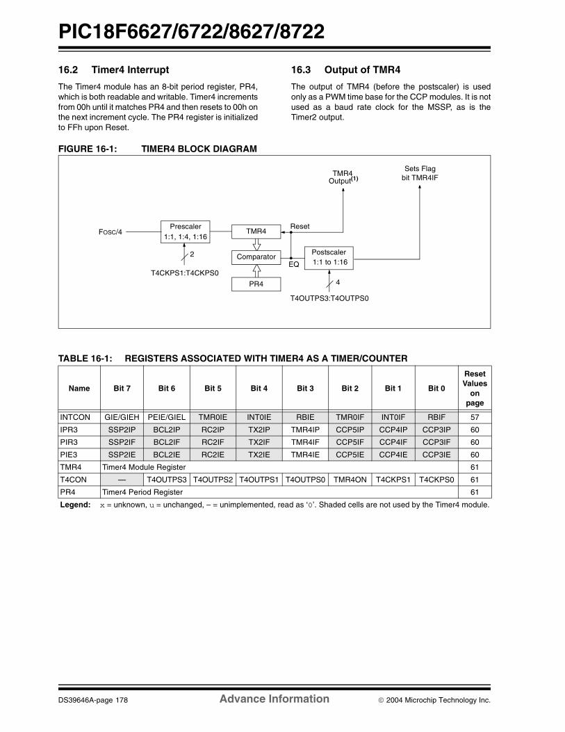
PIC18F6627/6722/8627/8722
DS39646A-page 178 Advance Information 2004 Microchip Technology Inc.
16.2 Timer4 Interrupt
The Timer4 module has an 8-bit period register, PR4,which is both readable and writable. Timer4 incrementsfrom 00h until it matches PR4 and then resets to 00h onthe next increment cycle. The PR4 register is initializedto FFh upon Reset.
16.3 Output of TMR4
The output of TMR4 (before the postscaler) is usedonly as a PWM time base for the CCP modules. It is notused as a baud rate clock for the MSSP, as is theTimer2 output.
FIGURE 16-1: TIMER4 BLOCK DIAGRAM
TABLE 16-1: REGISTERS ASSOCIATED WITH TIMER4 AS A TIMER/COUNTER
Comparator
TMR4Sets Flag
TMR4
Output(1)
Reset
Postscaler
Prescaler
PR4
2
FOSC/4
1:1 to 1:16
1:1, 1:4, 1:16
EQ
4
bit TMR4IF
T4OUTPS3:T4OUTPS0
T4CKPS1:T4CKPS0
Name Bit 7 Bit 6 Bit 5 Bit 4 Bit 3 Bit 2 Bit 1 Bit 0
Reset Values
on page
INTCON GIE/GIEH PEIE/GIEL TMR0IE INT0IE RBIE TMR0IF INT0IF RBIF 57
IPR3 SSP2IP BCL2IP RC2IP TX2IP TMR4IP CCP5IP CCP4IP CCP3IP 60
PIR3 SSP2IF BCL2IF RC2IF TX2IF TMR4IF CCP5IF CCP4IF CCP3IF 60
PIE3 SSP2IE BCL2IE RC2IE TX2IE TMR4IE CCP5IE CCP4IE CCP3IE 60
TMR4 Timer4 Module Register 61
T4CON — T4OUTPS3 T4OUTPS2 T4OUTPS1 T4OUTPS0 TMR4ON T4CKPS1 T4CKPS0 61
PR4 Timer4 Period Register 61
Legend: x = unknown, u = unchanged, – = unimplemented, read as ‘0’. Shaded cells are not used by the Timer4 module.

2004 Microchip Technology Inc. Advance Information DS39646A-page 179
PIC18F6627/6722/8627/8722
17.0 CAPTURE/COMPARE/PWM (CCP) MODULES
PIC18F6627/6722/8627/8722 devices all have a totalof five CCP (Capture/Compare/PWM) modules. Two ofthese (CCP4 and CCP5) implement standard Capture,Compare and Pulse-Width Modulation (PWM) modes,and are discussed in this section. The other threemodules (ECCP1, ECCP2, ECCP3) implementstandard Capture and Compare modes, as well asenhanced PWM modes. These are discussed inSection 18.0 “Enhanced Capture/Compare/PWM(ECCP) Module”.
Each CCP/ECCP module contains a 16-bit registerwhich can operate as a 16-bit Capture register, a 16-bitCompare register or a PWM Master/Slave Duty Cycleregister. For the sake of clarity, all CCP module opera-tions in the following sections are described withrespect to CCP4, but is equally applicable to CCP5.
Capture and Compare operations described in thischapter apply to all standard and enhanced CCP mod-ules. The operations of PWM mode described inSection 17.4 “PWM Mode” applies to CCP4 andCCP5 only.
REGISTER 17-1: CCPxCON: CCP CONTROL REGISTER (CCP4 AND CCP5 MODULES)
Note: Throughout this section andSection 18.0 “Enhanced Capture/Compare/PWM (ECCP) Module”,references to register and bit names thatmay be associated with a specific CCPmodule are referred to generically by theuse of ‘x’ or ‘y’ in place of the specificmodule number. Thus, “CCPxCON” mightrefer to the control register for CCP4 orCCP5, or ECCP1, ECCP2 or ECCP3.“CCPxCON” is used throughout thesesections to refer to the module controlregister, regardless of whether the CCPmodule is a standard or enhancedimplementation.
U-0 U-0 R/W-0 R/W-0 R/W-0 R/W-0 R/W-0 R/W-0
— — DCxB1 DCxB0 CCPxM3 CCPxM2 CCPxM1 CCPxM0
bit 7 bit 0
bit 7-6 Unimplemented: Read as ‘0’
bit 5-4 DCxB1:DCxB0: PWM Duty Cycle bit 1 and bit 0 for CCP Module xCapture mode:UnusedCompare mode:UnusedPWM mode:These bits are the two Least Significant bits (bit 1 and bit 0) of the 10-bit PWM duty cycle. The eight Most Significant bits (DCx9:DCx2) of the duty cycle are found in CCPRxL.
bit 3-0 CCPxM3:CCPxM0: CCP Module x Mode Select bits
0000 = Capture/Compare/PWM disabled (resets CCPx module) 0001 = Reserved 0010 = Compare mode, toggle output on match (CCPxIF bit is set) 0011 = Reserved 0100 = Capture mode, every falling edge 0101 = Capture mode, every rising edge0110 = Capture mode, every 4th rising edge 0111 = Capture mode, every 16th rising edge1000 = Compare mode; initialize CCP pin low; on compare match, force CCP pin high
(CCPIF bit is set) 1001 = Compare mode; initialize CCP pin high; on compare match, force CCP pin low
(CCPIF bit is set) 1010 = Compare mode; generate software interrupt on compare match (CCPIF bit is set,
CCP pin reflects I/O state) 1011 = Reserved11xx = PWM mode
Legend:
R = Readable bit W = Writable bit U = Unimplemented bit, read as ‘0’
-n = Value at POR ‘1’ = Bit is set ‘0’ = Bit is cleared x = Bit is unknown

PIC18F6627/6722/8627/8722
DS39646A-page 180 Advance Information 2004 Microchip Technology Inc.
17.1 CCP Module Configuration
Each Capture/Compare/PWM module is associatedwith a control register (generically, CCPxCON) and adata register (CCPRx). The data register, in turn, iscomprised of two 8-bit registers: CCPRxL (low byte)and CCPRxH (high byte). All registers are bothreadable and writable.
17.1.1 CCP MODULES AND TIMER RESOURCES
The CCP/ECCP modules utilize Timers 1, 2, 3 or 4,depending on the mode selected. Timer1 and Timer3are available to modules in Capture or Comparemodes, while Timer2 and Timer4 are available formodules in PWM mode.
TABLE 17-1: CCP MODE – TIMER RESOURCE
The assignment of a particular timer to a module isdetermined by the Timer-to-CCP enable bits in theT3CON register (Register 15-1). Depending on theconfiguration selected, up to four timers may be activeat once, with modules in the same configuration(Capture/Compare or PWM) sharing timer resources.The possible configurations are shown in Figure 17-1.
17.1.2 CCP2 PIN ASSIGNMENT
The pin assignment for CCP2 (Capture input, Compareand PWM output) can change, based on device config-uration. The CCP2MX configuration bit determineswhich pin CCP2 is multiplexed to. By default, it isassigned to RC1 (CCP2MX = 1). If the configuration bitis cleared, CCP2 is multiplexed with RE7 in Microcon-troller mode, or RE3 in all other modes.
Changing the pin assignment of CCP2 does not auto-matically change any requirements for configuring theport pin. Users must always verify that the appropriateTRIS register is configured correctly for CCP2operation, regardless of where it is located.
FIGURE 17-1: CCP AND TIMER INTERCONNECT CONFIGURATIONS
CCP Mode Timer Resource
CaptureCompare
PWM
Timer1 or Timer3Timer1 or Timer3Timer2 or Timer4
TMR1
CCP5
TMR2
TMR3
TMR4
CCP4
ECCP3
ECCP2
ECCP1
TMR1
TMR2
TMR3
CCP5
TMR4
CCP4
ECCP3
ECCP2
ECCP1
TMR1
TMR2
TMR3
CCP5
TMR4
CCP4
ECCP3
ECCP2
ECCP1
TMR1
TMR2
TMR3
CCP5
TMR4
CCP4
ECCP3
ECCP2
ECCP1
T3CCP<2:1> = 00 T3CCP<2:1> = 01 T3CCP<2:1> = 10 T3CCP<2:1> = 11
Timer1 is used for all Captureand Compare operations forall CCP modules. Timer2 isused for PWM operations forall CCP modules. Modulesmay share either timerresource as a common timebase.
Timer3 and Timer4 are notavailable.
Timer1 and Timer2 are usedfor Capture and Compare orPWM operations for ECCP1only (depending on selectedmode).
All other modules use eitherTimer3 or Timer4. Modulesmay share either timerresource as a common timebase if they are in Capture/Compare or PWM modes.
Timer1 and Timer2 are usedfor Capture and Compare orPWM operations for ECCP1and ECCP2 only (dependingon the mode selected for eachmodule). Both modules mayuse a timer as a common timebase if they are both inCapture/Compare or PWMmodes.
The other modules use eitherTimer3 or Timer4. Modulesmay share either timerresource as a common timebase if they are in Capture/Compare or PWM modes.
Timer3 is used for all Captureand Compare operations forall CCP modules. Timer4 isused for PWM operations forall CCP modules. Modulesmay share either timerresource as a common timebase.
Timer1 and Timer2 are notavailable.

2004 Microchip Technology Inc. Advance Information DS39646A-page 181
PIC18F6627/6722/8627/8722
17.2 Capture Mode
In Capture mode, the CCPRxH:CCPRxL register paircaptures the 16-bit value of the TMR1 or TMR3registers when an event occurs on the correspondingCCPx pin. An event is defined as one of the following:
• every falling edge
• every rising edge• every 4th rising edge• every 16th rising edge
The event is selected by the mode select bits,CCPxM3:CCPxM0 (CCPxCON<3:0>). When a captureis made, the interrupt request flag bit, CCPxIF, is set; itmust be cleared in software. If another capture occursbefore the value in register CCPRx is read, the oldcaptured value is overwritten by the new captured value.
17.2.1 CCP PIN CONFIGURATION
In Capture mode, the appropriate CCPx pin should beconfigured as an input by setting the correspondingTRIS direction bit.
17.2.2 TIMER1/TIMER3 MODE SELECTION
The timers that are to be used with the capture feature(Timer1 and/or Timer3) must be running in Timer mode orSynchronized Counter mode. In Asynchronous Countermode, the capture operation will not work. The timer to beused with each CCP module is selected in the T3CONregister (see Section 17.1.1 “CCP Modules and TimerResources”).
17.2.3 SOFTWARE INTERRUPT
When the Capture mode is changed, a false captureinterrupt may be generated. The user should keep theCCPxIE interrupt enable bit clear to avoid false inter-rupts. The interrupt flag bit, CCPxIF, should also becleared following any such change in Operating mode.
17.2.4 CCP PRESCALER
There are four prescaler settings in Capture mode; theyare specified as part of the Operating mode selected bythe mode select bits (CCPxM3:CCPxM0). Wheneverthe CCP module is turned off or Capture mode isdisabled, the prescaler counter is cleared. This meansthat any Reset will clear the prescaler counter.
Switching from one capture prescaler to another maygenerate an interrupt. Also, the prescaler counter willnot be cleared; therefore, the first capture may be froma non-zero prescaler. Example 17-1 shows therecommended method for switching between captureprescalers. This example also clears the prescalercounter and will not generate the “false” interrupt.
EXAMPLE 17-1: CHANGING BETWEEN CAPTURE PRESCALERS(CCP5 SHOWN)
FIGURE 17-2: CAPTURE MODE OPERATION BLOCK DIAGRAM
Note: If a CCPx pin is configured as an output, awrite to the port can cause a capturecondition.
CLRF CCP5CON ; Turn CCP module offMOVLW NEW_CAPT_PS ; Load WREG with the
; new prescaler mode; value and CCP ON
MOVWF CCP5CON ; Load CCP5CON with; this value
CCPR4H CCPR4L
TMR1H TMR1L
Set Flag bit CCP4IF
TMR3Enable
Q’sCCP1CON<3:0>
RG3/CCP4 pin
Prescaler÷ 1, 4, 16
andEdge Detect
TMR3H TMR3L
TMR1Enable
T3CCP2
T3CCP2

PIC18F6627/6722/8627/8722
DS39646A-page 182 Advance Information 2004 Microchip Technology Inc.
17.3 Compare Mode
In Compare mode, the 16-bit CCPRx register value isconstantly compared against either the TMR1 or TMR3register pair value. When a match occurs, the CCPx pincan be:
• driven high
• driven low• toggled (high-to-low or low-to-high) • remain unchanged (that is, reflects the state of the
I/O latch)
The action on the pin is based on the value of the modeselect bits (CCPxM3:CCPxM0). At the same time, theinterrupt flag bit, CCPxIF, is set.
17.3.1 CCP PIN CONFIGURATION
The user must configure the CCPx pin as an output byclearing the appropriate TRIS bit.
17.3.2 TIMER1/TIMER3 MODE SELECTION
Timer1 and/or Timer3 must be running in Timer modeor Synchronized Counter mode if the CCP module isusing the compare feature. In Asynchronous Countermode, the compare operation may not work.
17.3.3 SOFTWARE INTERRUPT MODE
When the Generate Software Interrupt mode is chosen(CCPxM3:CCPxM0 = 1010), the corresponding CCPxpin is not affected. Only a CCP interrupt is generated,if enabled and the CCPxIE bit is set.
17.3.4 SPECIAL EVENT TRIGGER
All CCP modules are equipped with a special eventtrigger. This is an internal hardware signal generated inCompare mode to trigger actions by other modules.The special event trigger is enabled by selectingthe Compare Special Event Trigger mode(CCPxM3:CCPxM0 = 1011).
For all CCP modules, the special event trigger resets thetimer register pair for whichever timer resource is cur-rently assigned as the module’s time base. This allowsthe CCPRx registers to serve as a programmable periodregister for either timer.
The ECCP2 special event trigger can also start an A/Dconversion. In order to do this, the A/D converter mustalready be enabled.
FIGURE 17-3: COMPARE MODE OPERATION BLOCK DIAGRAM
Note: Clearing the CCPxCON register will forcethe compare output latch (depending ondevice configuration) to the default lowlevel. This is not the PORT I/O data latch.
CCPR4H CCPR4L
TMR1H TMR1L
ComparatorQ S
R
OutputLogic
Special Event Trigger
Set Flag bit CCP4IF
MatchRG3/CCP4 pin
TRISG<3>CCP4CON<3:0>
Mode SelectOutput Enable
TMR3H TMR3L
T3CCP2 10
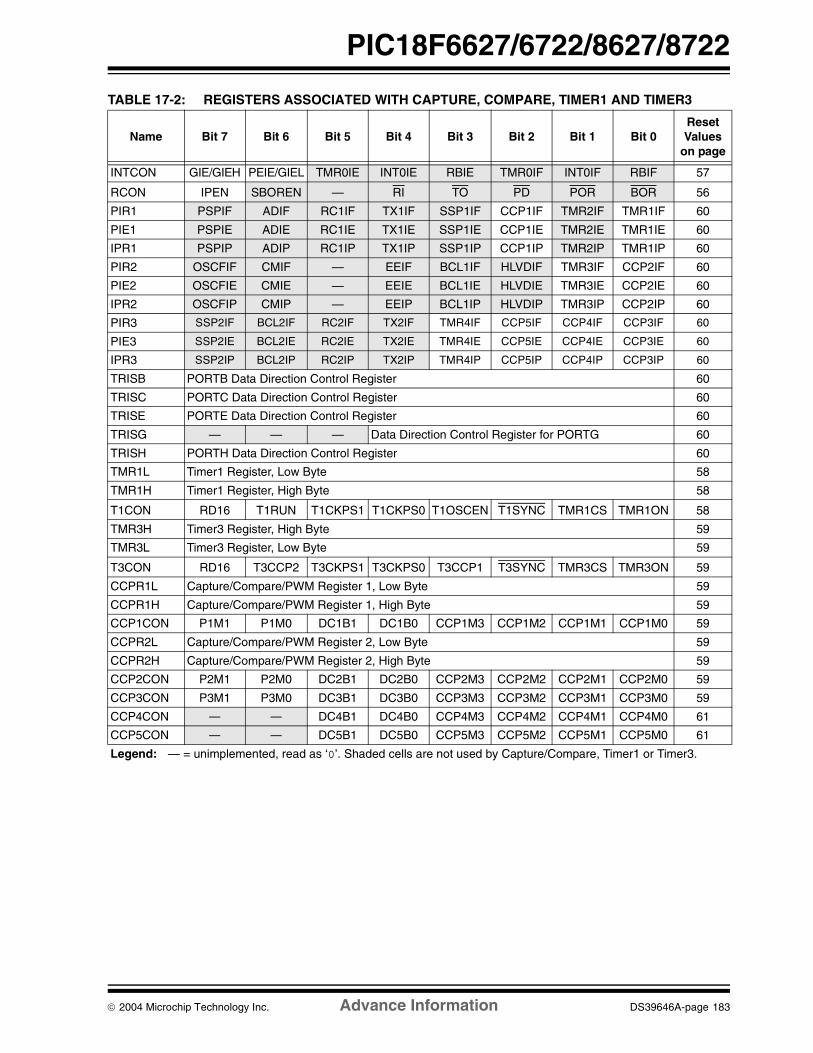
2004 Microchip Technology Inc. Advance Information DS39646A-page 183
PIC18F6627/6722/8627/8722
TABLE 17-2: REGISTERS ASSOCIATED WITH CAPTURE, COMPARE, TIMER1 AND TIMER3
Name Bit 7 Bit 6 Bit 5 Bit 4 Bit 3 Bit 2 Bit 1 Bit 0Reset Values
on page
INTCON GIE/GIEH PEIE/GIEL TMR0IE INT0IE RBIE TMR0IF INT0IF RBIF 57
RCON IPEN SBOREN — RI TO PD POR BOR 56
PIR1 PSPIF ADIF RC1IF TX1IF SSP1IF CCP1IF TMR2IF TMR1IF 60
PIE1 PSPIE ADIE RC1IE TX1IE SSP1IE CCP1IE TMR2IE TMR1IE 60
IPR1 PSPIP ADIP RC1IP TX1IP SSP1IP CCP1IP TMR2IP TMR1IP 60
PIR2 OSCFIF CMIF — EEIF BCL1IF HLVDIF TMR3IF CCP2IF 60
PIE2 OSCFIE CMIE — EEIE BCL1IE HLVDIE TMR3IE CCP2IE 60
IPR2 OSCFIP CMIP — EEIP BCL1IP HLVDIP TMR3IP CCP2IP 60
PIR3 SSP2IF BCL2IF RC2IF TX2IF TMR4IF CCP5IF CCP4IF CCP3IF 60
PIE3 SSP2IE BCL2IE RC2IE TX2IE TMR4IE CCP5IE CCP4IE CCP3IE 60
IPR3 SSP2IP BCL2IP RC2IP TX2IP TMR4IP CCP5IP CCP4IP CCP3IP 60
TRISB PORTB Data Direction Control Register 60
TRISC PORTC Data Direction Control Register 60
TRISE PORTE Data Direction Control Register 60
TRISG — — — Data Direction Control Register for PORTG 60
TRISH PORTH Data Direction Control Register 60
TMR1L Timer1 Register, Low Byte 58
TMR1H Timer1 Register, High Byte 58
T1CON RD16 T1RUN T1CKPS1 T1CKPS0 T1OSCEN T1SYNC TMR1CS TMR1ON 58
TMR3H Timer3 Register, High Byte 59
TMR3L Timer3 Register, Low Byte 59
T3CON RD16 T3CCP2 T3CKPS1 T3CKPS0 T3CCP1 T3SYNC TMR3CS TMR3ON 59
CCPR1L Capture/Compare/PWM Register 1, Low Byte 59
CCPR1H Capture/Compare/PWM Register 1, High Byte 59
CCP1CON P1M1 P1M0 DC1B1 DC1B0 CCP1M3 CCP1M2 CCP1M1 CCP1M0 59
CCPR2L Capture/Compare/PWM Register 2, Low Byte 59
CCPR2H Capture/Compare/PWM Register 2, High Byte 59
CCP2CON P2M1 P2M0 DC2B1 DC2B0 CCP2M3 CCP2M2 CCP2M1 CCP2M0 59
CCP3CON P3M1 P3M0 DC3B1 DC3B0 CCP3M3 CCP3M2 CCP3M1 CCP3M0 59
CCP4CON — — DC4B1 DC4B0 CCP4M3 CCP4M2 CCP4M1 CCP4M0 61
CCP5CON — — DC5B1 DC5B0 CCP5M3 CCP5M2 CCP5M1 CCP5M0 61
Legend: — = unimplemented, read as ‘0’. Shaded cells are not used by Capture/Compare, Timer1 or Timer3.

PIC18F6627/6722/8627/8722
DS39646A-page 184 Advance Information 2004 Microchip Technology Inc.
17.4 PWM Mode
In Pulse Width Modulation (PWM) mode, the CCPx pinproduces up to a 10-bit resolution PWM output. Sincethe CCP4 and CCP5 pins are multiplexed with aPORTG data latch, the appropriate TRISG bit must becleared to make the CCP4 or CCP5 pin an output.
Figure 17-4 shows a simplified block diagram of theCCP module in PWM mode.
For a step-by-step procedure on how to set up a CCPmodule for PWM operation, see Section 17.4.3“Setup for PWM Operation”.
FIGURE 17-4: SIMPLIFIED PWM BLOCK DIAGRAM
A PWM output (Figure 17-5) has a time base (period)and a time that the output stays high (duty cycle).The frequency of the PWM is the inverse of theperiod (1/period).
FIGURE 17-5: PWM OUTPUT
17.4.1 PWM PERIOD
The PWM period is specified by writing to the PR2(PR4) register. The PWM period can be calculatedusing the following formula:
EQUATION 17-1:
PWM frequency is defined as 1/[PWM period].
When TMR2 (TMR4) is equal to PR2 (PR4), thefollowing three events occur on the next incrementcycle:
• TMR2 (TMR4) is cleared• The CCPx pin is set (exception: if PWM duty
cycle = 0%, the CCPx pin will not be set)• The PWM duty cycle is latched from CCPRxL into
CCPRxH
17.4.2 PWM DUTY CYCLE
The PWM duty cycle is specified by writing to theCCPRxL register and to the CCPxCON<5:4> bits. Upto 10-bit resolution is available. The CCPRxL containsthe eight MSbs and the CCPxCON<5:4> contains thetwo LSbs. This 10-bit value is represented byCCPRxL:CCPxCON<5:4>. The following equation isused to calculate the PWM duty cycle in time:
EQUATION 17-2:
CCPRxL and CCPxCON<5:4> can be written to at anytime, but the duty cycle value is not latched intoCCPRxH until after a match between PR2 (PR4) andTMR2 (TMR4) occurs (i.e., the period is complete). InPWM mode, CCPRxH is a read-only register.
Note: Clearing the CCP4CON or CCP5CONregister will force the RG3 or RG4 outputlatch (depending on device configuration)to the default low level. This is not thePORTG I/O data latch.
CCPRxL
CCPRxH (Slave)
Comparator
TMR2 (TMR4)
Comparator
PR2 (PR4)
(Note 1)
R Q
S
Duty Cycle Registers CCPxCON<5:4>
Clear Timer,CCPx pin and latch D.C.
Note 1: The 8-bit TMR2 or TMR4 value is concatenated with the 2-bit internal Q clock, or 2 bits of the prescaler, to create the 10-bit time base.
CCPx Output
CorrespondingTRIS bit
Period
Duty Cycle
TMR2 (TMR4) = PR2 (TMR4)
TMR2 (TMR4) = Duty Cycle
TMR2 (TMR4) = PR2 (PR4)
Note: The Timer2 and Timer 4 postscalers (seeSection 14.0 “Timer2 Module” andSection 16.0 “Timer4 Module”) are notused in the determination of the PWMfrequency. The postscaler could be usedto have a servo update rate at a differentfrequency than the PWM output.
PWM Period = [(PR2) + 1] • 4 • TOSC •(TMR2 Prescale Value)
PWM Duty Cycle = (CCPRXL:CCPXCON<5:4>) •TOSC • (TMR2 Prescale Value)

2004 Microchip Technology Inc. Advance Information DS39646A-page 185
PIC18F6627/6722/8627/8722
The CCPRxH register and a 2-bit internal latch areused to double-buffer the PWM duty cycle. Thisdouble-buffering is essential for glitchless PWMoperation.
When the CCPRxH and 2-bit latch match TMR2(TMR4), concatenated with an internal 2-bit Q clock or2 bits of the TMR2 (TMR4) prescaler, the CCPx pin iscleared.
The maximum PWM resolution (bits) for a given PWMfrequency is given by the equation:
EQUATION 17-3:
17.4.3 SETUP FOR PWM OPERATION
The following steps should be taken when configuringthe CCP module for PWM operation:
1. Set the PWM period by writing to the PR2 (PR4)register.
2. Set the PWM duty cycle by writing to theCCPRxL register and CCPxCON<5:4> bits.
3. Make the CCPx pin an output by clearing theappropriate TRIS bit.
4. Set the TMR2 (TMR4) prescale value, thenenable Timer2 (Timer4) by writing to T2CON(T4CON).
5. Configure the CCPx module for PWM operation.
TABLE 17-3: EXAMPLE PWM FREQUENCIES AND RESOLUTIONS AT 40 MHz
Note: If the PWM duty cycle value is longer thanthe PWM period, the CCPx pin will not becleared.
FOSC
FPWM--------------- log
2( )log-----------------------------bits=PWM Resolution (max)
PWM Frequency 2.44 kHz 9.77 kHz 39.06 kHz 156.25 kHz 312.50 kHz 416.67 kHz
Timer Prescaler (1, 4, 16) 16 4 1 1 1 1
PR2 Value FFh FFh FFh 3Fh 1Fh 17h
Maximum Resolution (bits) 10 10 10 8 7 6.58

PIC18F6627/6722/8627/8722
DS39646A-page 186 Advance Information 2004 Microchip Technology Inc.
TABLE 17-4: REGISTERS ASSOCIATED WITH PWM, TIMER2 AND TIMER4
Name Bit 7 Bit 6 Bit 5 Bit 4 Bit 3 Bit 2 Bit 1 Bit 0Reset Values
on page
INTCON GIE/GIEH PEIE/GIEL TMR0IE INT0IE RBIE TMR0IF INT0IF RBIF 57
RCON IPEN SBOREN — RI TO PD POR BOR 56
PIR1 PSPIF ADIF RC1IF TX1IF SSP1IF CCP1IF TMR2IF TMR1IF 60
PIE1 PSPIE ADIE RC1IE TX1IE SSP1IE CCP1IE TMR2IE TMR1IE 60
IPR1 PSPIP ADIP RC1IP TX1IP SSP1IP CCP1IP TMR2IP TMR1IP 60
PIR3 SSP2IF BCL2IF RC2IF TX2IF TMR4IF CCP5IF CCP4IF CCP3IF 60
PIE3 SSP2IE BCL2IF RC2IE TX2IE TMR4IE CCP5IE CCP4IE CCP3IE 60
IPR3 SSP2IP BCL2IP RC2IP TX2IP TMR4IP CCP5IP CCP4IP CCP3IP 60
TMR2 Timer2 Register 58
PR2 Timer2 Period Register 58
T2CON — T2OUTPS3 T2OUTPS2 T2OUTPS1 T2OUTPS0 TMR2ON T2CKPS1 T2CKPS0 58
TMR4 Timer4 Register 61
PR4 Timer4 Period Register 61
T4CON — T4OUTPS3 T4OUTPS2 T4OUTPS1 T4OUTPS0 TMR4ON T4CKPS1 T4CKPS0 61
CCPR1L Capture/Compare/PWM Register 1, Low Byte 59
CCPR1H Capture/Compare/PWM Register 1, High Byte 59
CCPR2L Capture/Compare/PWM Register 2, Low Byte 59
CCPR2H Capture/Compare/PWM Register 2, High Byte 59
CCP4CON — — DC4B1 DC4B0 CCP4M3 CCP4M2 CCP4M1 CCP4M0 61
CCP5CON — — DC5B1 DC5B0 CCP5M3 CCP5M2 CCP5M1 CCP5M0 61
Legend: x = unknown, u = unchanged, – = unimplemented, read as ‘0’. Shaded cells are not used by PWM,Timer2 or Timer4.

2004 Microchip Technology Inc. Advance Information DS39646A-page 187
PIC18F6627/6722/8627/8722
18.0 ENHANCED CAPTURE/COMPARE/PWM (ECCP) MODULE
In PIC18F6627/6722/8627/8722 devices, ECCP1,ECCP2 and ECCP3 are implemented as a standardCCP module with enhanced PWM capabilities. Theseinclude the provision for 2 or 4 output channels, userselectable polarity, dead-band control and automaticshutdown and restart. The enhanced features arediscussed in detail in Section 18.4 “Enhanced PWMMode”. Capture, Compare and single-output PWMfunctions of the ECCP module are the same asdescribed for the standard CCP module.
The control register for the enhanced CCP module isshown in Register 18-1. It differs from the CCPxCONregisters in PIC18F6627/6722/8627/8722 devices inthat the two Most Significant bits are implemented tocontrol PWM functionality. In addition to the expandedrange of modes available through the ECCPxCONregister, the ECCP modules each have two additionalfeatures associated with enhanced PWM operationand Auto-Shutdown features. They are:
• ECCPxDEL (Dead Band delay)• ECCPxAS (Auto-Shutdown configuration)
REGISTER 18-1: ECCPxCON: ENHANCED CCP CONTROL REGISTER (ECCP1, ECCP2 AND ECCP3 MODULES)
R/W-0 R/W-0 R/W-0 R/W-0 R/W-0 R/W-0 R/W-0 R/W-0
PxM1 PxM0 DCxB1 DCxB0 CCPxM3 CCPxM2 CCPxM1 CCPxM0
bit 7 bit 0
bit 7-6 PxM1:PxM0: Enhanced PWM Output Configuration bitsIf CCPxM3:CCPxM2 = 00, 01, 10:xx = PxA assigned as Capture/Compare input/output; PxB, PxC, PxD assigned as port pinsIf CCPxM3:CCPxM2 = 11:00 = Single output: PxA modulated, PxB, PxC, PxD assigned as port pins01 = Full-bridge output forward: P1D modulated; P1A active; P1B, P1C inactive10 = Half-bridge output: P1A, P1B modulated with dead-band control; P1C, P1D assigned
as port pins11 = Full-bridge output reverse: P1B modulated; P1C active; P1A, P1D inactive
bit 5-4 DCxB1:DCxB0: PWM Duty Cycle bit 1 and bit 0Capture mode:Unused.Compare mode: Unused.PWM mode: These bits are the two LSbs of the 10-bit PWM duty cycle. The eight MSbs of the duty cycle are found in CCPRxL.
bit 3-0 CCPxM3:CCPxM0: Enhanced CCP Mode Select bits0000 = Capture/Compare/PWM off (resets CCPx module)0001 = Reserved 0010 = Compare mode, toggle output on match0011 = Capture mode0100 = Capture mode, every falling edge 0101 = Capture mode, every rising edge0110 = Capture mode, every 4th rising edge 0111 = Capture mode, every 16th rising edge1000 = Compare mode, initialize CCP pin low, set output on compare match (set CCPxIF)1001 = Compare mode, initialize CCP pin high, clear output on compare match (set CCPxIF)1010 = Compare mode, generate software interrupt only, CCP pin reverts to I/O state1011 = Compare mode, trigger special event (ECCP resets TMR1 or TMR3, sets CCPxIF bit,
ECCP2 trigger starts A/D conversion if A/D module is enabled)1100 = PWM mode; PxA, PxC active-high; PxB, PxD active-high1101 = PWM mode; PxA, PxC active-high; PxB, PxD active-low1110 = PWM mode; PxA, PxC active-low; PxB, PxD active-high1111 = PWM mode; PxA, PxC active-low; PxB, PxD active-low
Legend:
R = Readable bit W = Writable bit U = Unimplemented bit, read as ‘0’
-n = Value at POR ‘1’ = Bit is set ‘0’ = Bit is cleared x = Bit is unknown

PIC18F6627/6722/8627/8722
DS39646A-page 188 Advance Information 2004 Microchip Technology Inc.
18.1 ECCP Outputs and Configuration
Each of the enhanced CCP modules may have up tofour PWM outputs, depending on the selectedoperating mode. These outputs, designated PxAthrough PxD, are multiplexed with various I/O pins.Some ECCP pin assignments are constant, whileothers change based on device configuration. Forthose pins that do change, the controlling bits are:
• CCP2MX configuration bit (CONFIG3H<0>)
• ECCPMX configuration bit (CONFIG3H<1>)• Program Memory mode (set by configuration bits
CONFIG3L<1:0>)
The pin assignments for the enhanced CCP modulesare summarized in Table 18-1, Table 18-2 andTable 18-3. To configure the I/O pins as PWM outputs,the proper PWM mode must be selected by setting thePxMx and CCPxMx bits (ECCPxCON<7:6> and <3:0>,respectively). The appropriate TRIS direction bits forthe corresponding port pins must also be set asoutputs.
18.1.1 USE OF CCP4 AND CCP5 WITH ECCP1 AND ECCP3
Only the ECCP2 module has four dedicated output pinsavailable for use. Assuming that the I/O ports or othermultiplexed functions on those pins are not needed,they may be used whenever needed without interferingwith any other CCP module.
ECCP1 and ECCP3, on the other hand, only havethree dedicated output pins: CCPx/P3A, PxB, and PxC.Whenever these modules are configured for QuadPWM mode, the pin used for CCP4 or CCP5 takespriority over the D output pins for ECCP3 and ECCP1,respectively.
18.1.2 ECCP MODULE OUTPUTS, PROGRAM MEMORY MODES, AND EMB ADDRESS BUS WIDTH
For PIC18F8627/8722 devices, the Program Memorymode of the device (Section 7.2 “Address and DataWidth” and Section 7.4 “Program Memory Modesand the External Memory Bus”) impacts both pinmultiplexing and the operation of the module.
The ECCP2 input/output (CCP2/P2A) can be multi-plexed to one of three pins. By default, this is RC1 forall devices; in this case, the default is when CCP2MXis set and the device is operating in Microcontrollermode. With PIC18F8627/8722 devices, three otheroptions exist. When CCP2MX is not set (= 0) and thedevice is in Microcontroller mode, CCP2/P2A is multi-plexed to RE7; in all other program memory modes, itis multiplexed to RB3.
Another option is for ECCPMX to be set while thedevice is operating in one of the three other programmemory modes. In this case, ECCP1 and ECCP3 oper-ate as compatible (i.e., single output) CCP modules.The pins used by their other outputs (PxB through PxD)are available for other multiplexed functions. ECCP2continues to operate as an enhanced CCP moduleregardless of the program memory mode.
The final option is for the ABW<1:0> configuration bitswhich select 8, 12, 16 or 20-bit EMB addressing. Pinsnot assigned to EMB address pins are available forperipheral or port functions.

2004 Microchip Technology Inc. Advance Information DS39646A-page 189
PIC18F6627/6722/8627/8722
TABLE 18-1: PIN CONFIGURATIONS FOR ECCP1
ECCP ModeCCP1CON
ConfigurationRC2 RE6 RE5 RG4 RH7 RH6
All PIC18F6627/6722 devices:
Compatible CCP 00xx 11xx CCP1 RE6 RE5 RG4/CCP5 N/A N/A
Dual PWM 10xx 11xx P1A P1B RE5 RG4/CCP5 N/A N/A
Quad PWM x1xx 11xx P1A P1B P1C P1D/CCP5(1) N/A N/A
PIC18F8627/8722 devices, ECCPMX = 1, Microcontroller mode:
Compatible CCP 00xx 11xx CCP1 RE6 RE5 RG4/CCP5 RH7/AN15 RH6/AN14
Dual PWM 10xx 11xx P1A P1B RE5 RG4/CCP5 RH7/AN15 RH6/AN14
Quad PWM x1xx 11xx P1A P1B P1C P1D/CCP5(1) RH7/AN15 RH6/AN14
PIC18F8627/8722 devices, ECCPMX = 0, Microcontroller mode:
Compatible CCP 00xx 11xx CCP1 RE6 RE5 RG4/CCP5 RH7/AN15 RH6/AN14
Dual PWM 10xx 11xx P1A RE6 RE5 RG4/CCP5 P1B RH6/AN14
Quad PWM x1xx 11xx P1A RE6 RE5 P1D/CCP5(1) P1B P1C
PIC18F8627/8722 devices, ECCPMX = 1, all other Program Memory modes:
Compatible CCP 00xx 11xx CCP1 AD14(2) AD13(2) RG4/CCP5 RH7/AN15 RH6/AN14
Dual PWM 10xx 11xx P1A P1B/AD14(2) AD13(2) RG4/CCP5 RH7/AN15 RH6/AN14
Quad PWM x1xx 11xx P1A P1B/AD14(2) P1C/AD13(2) P1D/CCP5(1) RH7/AN15 RH6/AN14
PIC18F8627/8722 devices, ECCPMX = 0, all other Program Memory modes:
Compatible CCP 00xx 11xx CCP1 AD14(2) AD13(2) RG4/CCP5 RH7/AN15 RH6/AN14
Dual PWM 10xx 11xx P1A AD14(2) AD13(2) RG4/CCP5 P1B RH6/AN14
Quad PWM x1xx 11xx P1A AD14(2) AD13(2) P1D/CCP5(1) P1B P1C
Legend: x = Don’t care, N/A = Not available. Shaded cells indicate pin assignments not used by ECCP1 in a given mode.Note 1: With ECCP1 in Quad PWM mode, CCP5’s output overrides P1D.
2: The EMB address bus width will determine whether the pin will perform an EMB or port/peripheral function.

PIC18F6627/6722/8627/8722
DS39646A-page 190 Advance Information 2004 Microchip Technology Inc.
TABLE 18-2: PIN CONFIGURATIONS FOR ECCP2
ECCP ModeCCP2CON
ConfigurationRB3 RC1 RE7 RE2 RE1 RE0
All PIC18F6627/6722 devices, CCP2MX = 1:
Compatible CCP 00xx 11xx RB3/INT3 CCP2 RE7 RE2 RE1 RE0
Dual PWM 10xx 11xx RB3/INT3 P2A RE7 P2B RE1 RE0
Quad PWM x1xx 11xx RB3/INT3 P2A RE7 P2B P2C P2D
All PIC18F6627/6722 CCP2MX = 0:
Compatible CCP 00xx 11xx RB3/INT3 RC1/T1OSI CCP2 RE2 RE1 RE0
Dual PWM 10xx 11xx RB3/INT3 RC1/T1OSI P2A P2B RE1 RE0
Quad PWM x1xx 11xx RB3/INT3 RC1/T1OSI P2A P2B P2C P2D
PIC18F8627/8722 devices, CCP2MX = 1, Microcontroller mode:
Compatible CCP 00xx 11xx RB3/INT3 CCP2 RE7 RE2 RE1 RE0
Dual PWM 10xx 11xx RB3/INT3 P2A RE7 P2B RE1 RE0
Quad PWM x1xx 11xx RB3/INT3 P2A RE7 P2B P2C P2D
PIC18F8627/8722 devices, CCP2MX = 0, Microcontroller mode:
Compatible CCP 00xx 11xx RB3/INT3 RC1/T1OSCI CCP2 RE2 RE1 RE0
Dual PWM 10xx 11xx RB3/INT3 RC1/T1OSCI P2A P2B RE1 RE0
Quad PWM x1xx 11xx RB3/INT3 RC1/T1OSCI P2A P2B P2C P2D
PIC18F8627/8722 devices, CCP2MX = 1, all other Program Memory modes:
Compatible CCP 00xx 11xx RB3/INT3 CCP2 AD15(1) AD10(1) AD9(1) AD8(1)
Dual PWM 10xx 11xx RB3/INT3 P2A AD15(1) P2B/AD10(1) AD9(1) AD8(1)
Quad PWM x1xx 11xx RB3/INT3 P2A AD15(1) P2B/AD10(1) P2C/AD9(1) P2D/AD8(1)
PIC18F8627/8722 devices, CCP2MX = 0, all other Program Memory modes:
Compatible CCP 00xx 11xx CCP2 RC1/T1OSCI AD15(1) AD10(1) AD9(1) AD8(1)
Dual PWM 10xx 11xx P2A RC1/T1OSCI AD15(1) P2B/AD10(1) AD9(1) AD8(1)
Quad PWM x1xx 11xx P2A RC1/T1OSCI AD15(1) P2B/AD10(1) P2C/AD9(1) P2D/AD8(1)
Legend: x = Don’t care. Shaded cells indicate pin assignments not used by ECCP2 in a given mode.Note 1: The EMB address bus width will determine whether the pin will perform an EMB or port/peripheral function.

2004 Microchip Technology Inc. Advance Information DS39646A-page 191
PIC18F6627/6722/8627/8722
TABLE 18-3: PIN CONFIGURATIONS FOR ECCP3
18.1.3 ECCP MODULES AND TIMER RESOURCES
Like the standard CCP modules, the ECCP modulescan utilize Timers 1, 2, 3 or 4, depending on the modeselected. Timer1 and Timer3 are available for modulesin Capture or Compare modes, while Timer2 andTimer4 are available for modules in PWM mode. Addi-tional details on timer resources are provided inSection 17.1.1 “CCP Modules and TimerResources”.
ECCP ModeCCP3CON
ConfigurationRG0 RE4 RE3 RG3 RH5 RH4
All PIC18F6627/6722 devices:
Compatible CCP 00xx 11xx CCP3 RE4 RE3 RG3/CCP4 N/A N/A
Dual PWM 10xx 11xx P3A P3B RE3 RG3/CCP4 N/A N/A
Quad PWM x1xx 11xx P3A P3B P3C P3D/CCP4(1) N/A N/A
PIC18F8627/8722 devices, ECCPMX = 1, Microcontroller mode:
Compatible CCP 00xx 11xx CCP3 RE4 RE3 RG3/CCP4 RH5/AN13 RH4/AN12
Dual PWM 10xx 11xx P3A P3B RE3 RG3/CCP4 RH5/AN13 RH4/AN12
Quad PWM x1xx 11xx P3A P3B P3C P3D/CCP4(1) RH5/AN13 RH4/AN12
PIC18F8627/8722 devices, ECCPMX = 0, Microcontroller mode:
Compatible CCP 00xx 11xx CCP3 RE4 RE3 RG3/CCP4 RH5/AN13 RH4/AN12
Dual PWM 10xx 11xx P3A RE4 RE3 RG3/CCP4 P3B RH4/AN12
Quad PWM x1xx 11xx P3A RE4 RE3 P3D/CCP4(1) P3B P3C
PIC18F8627/8722 devices, ECCPMX = 1, all other Program Memory modes:
Compatible CCP 00xx 11xx CCP3 AD12(2) AD10(2) RG3/CCP4 RH5/AN13 RH4/AN12
Dual PWM 10xx 11xx P3A P3B/AD12(2) AD10(2) RG3/CCP4 RH5/AN13 RH4/AN12
Quad PWM x1xx 11xx P3A P3B/AD12(2) P3C/AD10(1) P3D/CCP4(1) RH5/AN13 RH4/AN12
PIC18F8627/8722 devices, ECCPMX = 0, all other Program Memory modes:
Compatible CCP 00xx 11xx CCP3 AD12(2) AD10(2) RG3/CCP4 RH5/AN13 RH4/AN12
Dual PWM 10xx 11xx P3A AD12(2) AD10(2) RG3/CCP4 P3B RH4/AN12
Quad PWM x1xx 11xx P3A AD12(2) AD10(2) P3D/CCP4(1) P3B P3C
Legend: x = Don’t care, N/A = Not available. Shaded cells indicate pin assignments not used by ECCP3 in a given mode.Note 1: With ECCP3 in Quad PWM mode, CCP4’s output overrides P3D.
2: The EMB address bus width will determine whether the pin will perform an EMB or port/peripheral function.

PIC18F6627/6722/8627/8722
DS39646A-page 192 Advance Information 2004 Microchip Technology Inc.
18.2 Capture and Compare Modes
With the exception of the special event triggerdiscussed below, the Capture and Compare modes ofthe ECCP modules are identical in operation to that ofCCP4. These are discussed in detail in Section 17.2“Capture Mode” and Section 17.3 “CompareMode”.
18.2.1 SPECIAL EVENT TRIGGER
The special event trigger output of ECCPx resets theTMR1 or TMR3 register pair, depending on which timerresource is currently selected. This allows the CCPRxregister to effectively be a 16-bit programmable periodregister for Timer1 or Timer3.
18.3 Standard PWM Mode
When configured in Single Output mode, the ECCPmodule functions identically to the standard CCPmodule in PWM mode as described in Section 17.4“PWM Mode”. This is also sometimes referred to as“Compatible CCP” mode as in Tables 18-1through 18-3.
18.4 Enhanced PWM Mode
The Enhanced PWM mode provides additional PWMoutput options for a broader range of control applica-tions. The module is a backward compatible version ofthe standard CCP module and offers up to four outputs,designated PxA through PxD. Users are also able toselect the polarity of the signal (either active-high oractive-low). The module’s Output mode and polarityare configured by setting the PxM1:PxM0 andCCPxM3CCPxM0 bits of the ECCPxCON register(ECCPxCON<7:6> and ECCPxCON<3:0>, respec-tively).
For the sake of clarity, Enhanced PWM mode operationis described generically throughout this section withrespect to ECCP1 and TMR2 modules. Control registernames are presented in terms of ECCP1. All threeenhanced modules, as well as the two timer resources,can be used interchangeably and function identically.TMR2 or TMR4 can be selected for PWM operation byselecting the proper bits in T3CON.
Figure 18-1 shows a simplified block diagram of PWMoperation. All control registers are double-buffered andare loaded at the beginning of a new PWM cycle (theperiod boundary when Timer2 resets) in order to pre-vent glitches on any of the outputs. The exception is thePWM delay register, ECCP1DEL, which is loaded ateither the duty cycle boundary or the boundary period(whichever comes first). Because of the buffering, themodule waits until the assigned timer resets instead ofstarting immediately. This means that enhanced PWMwaveforms do not exactly match the standard PWMwaveforms, but are instead offset by one full instructioncycle (4 TOSC).
As before, the user must manually configure theappropriate TRIS bits for output.
18.4.1 PWM PERIOD
The PWM period is specified by writing to the PR2register. The PWM period can be calculated using theequation:
PWM frequency is defined as 1/[PWM period]. WhenTMR2 is equal to PR2, the following three events occuron the next increment cycle:
• TMR2 is cleared
• The CCP1 pin is set (if PWM duty cycle = 0%, the CCP1 pin will not be set)
• The PWM duty cycle is copied from CCPR1L into CCPR1H
Note: When setting up single output PWM opera-tions, users are free to use either of theprocesses described in Section 17.4.3“Setup for PWM Operation” orSection 18.4.9 “Setup for PWM Opera-tion”. The latter is more generic, but willwork for either single or multi-output PWM.
Note: The Timer2 postscaler (see Section 14.0“Timer2 Module”) is not used in thedetermination of the PWM frequency. Thepostscaler could be used to have a servoupdate rate at a different frequency thanthe PWM output.
PWM Period = [(PR2) + 1] • 4 • TOSC •(TMR2 Prescale Value)

2004 Microchip Technology Inc. Advance Information DS39646A-page 193
PIC18F6627/6722/8627/8722
FIGURE 18-1: SIMPLIFIED BLOCK DIAGRAM OF THE ENHANCED PWM MODULE
18.4.2 PWM DUTY CYCLE
The PWM duty cycle is specified by writing to theCCPR1L register and to the CCP1CON<5:4> bits. Upto 10-bit resolution is available. The CCPR1L containsthe eight MSbs and the CCP1CON<5:4> contains thetwo LSbs. This 10-bit value is represented byCCPRxL:ECCPxCON<5:4>. The PWM duty cycle iscalculated by the equation:
CCPR1L and CCP1CON<5:4> can be written to at anytime but the duty cycle value is not copied intoCCPR1H until a match between PR2 and TMR2 occurs(i.e., the period is complete). In PWM mode, CCPR1His a read-only register.
The CCPRxH register and a 2-bit internal latch areused to double-buffer the PWM duty cycle. Thisdouble-buffering is essential for glitchless PWM opera-tion. When the CCPR1H and 2-bit latch match TMR2,concatenated with an internal 2-bit Q clock or two bitsof the TMR2 prescaler, the CCP1 pin is cleared. Themaximum PWM resolution (bits) for a given PWMfrequency is given by the equation:
TABLE 18-4: EXAMPLE PWM FREQUENCIES AND RESOLUTIONS AT 40 MHz
CCPR1L
CCPR1H (Slave)
Comparator
TMR2
Comparator
PR2
(Note 1)
R Q
S
Duty Cycle RegistersCCP1CON<5:4>
Clear Timer,set CCP1 pin and latch D.C.
Note: The 8-bit timer TMR2 register is concatenated with the 2-bit internal Q clock, or 2 bits of the prescaler, to create the 10-bittime base.
TRISx<x>
CCP1/P1A
TRISx<x>
P1B
TRISx<x>
TRISx<x>
P1D
OutputController
P1M1<1:0>2
CCP1M<3:0>4
ECCP1DEL
CCP1/P1A
P1B
P1C
P1D
P1C
PWM Duty Cycle = (CCPR1L:CCP1CON<5:4>) •TOSC • (TMR2 Prescale Value)
Note: If the PWM duty cycle value is longer thanthe PWM period, the CCP1 pin will not becleared.
( )PWM Resolution (max) =
FOSC
FPWMlog
log(2)bits
PWM Frequency 2.44 kHz 9.77 kHz 39.06 kHz 156.25 kHz 312.50 kHz 416.67 kHz
Timer Prescaler (1, 4, 16) 16 4 1 1 1 1
PR2 Value FFh FFh FFh 3Fh 1Fh 17h
Maximum Resolution (bits) 10 10 10 8 7 6.58

PIC18F6627/6722/8627/8722
DS39646A-page 194 Advance Information 2004 Microchip Technology Inc.
18.4.3 PWM OUTPUT CONFIGURATIONS
The P1M1:P1M0 bits in the CCP1CON register allowone of four configurations:
• Single Output• Half-Bridge Output
• Full-Bridge Output, Forward mode• Full-Bridge Output, Reverse mode
The Single Output mode is the standard PWM modediscussed in Section 18.4 “Enhanced PWM Mode”.The Half-Bridge and Full-Bridge Output modes arecovered in detail in the sections that follow.
The general relationship of the outputs in allconfigurations is summarized in Figure 18-2.
FIGURE 18-2: PWM OUTPUT RELATIONSHIPS (ACTIVE-HIGH STATE)0
Period
00
10
01
11
SIGNALPR2+1
CCP1CON<7:6>
P1A Modulated
P1A Modulated
P1B Modulated
P1A Active
P1B Inactive
P1C Inactive
P1D Modulated
P1A Inactive
P1B Modulated
P1C Active
P1D Inactive
DutyCycle
(Single Output)
(Half-Bridge)
(Full-Bridge,Forward)
(Full-Bridge,Reverse)
Delay(1) Delay(1)
Relationships:
• Period = 4 * TOSC * (PR2 + 1) * (TMR2 prescale value)• Duty Cycle = TOSC * (CCPR1L<7:0>:CCP1CON<5:4>) * (TMR2 prescale value)• Delay = 4 * TOSC * (ECCP1DEL<6:0>)Note 1: Dead-band delay is programmed using the ECCP1DEL register (Section 18.4.6 “Programmable
Dead-Band Delay”).

2004 Microchip Technology Inc. Advance Information DS39646A-page 195
PIC18F6627/6722/8627/8722
FIGURE 18-3: PWM OUTPUT RELATIONSHIPS (ACTIVE-LOW STATE)
18.4.4 HALF-BRIDGE MODE
In the Half-Bridge Output mode, two pins are used asoutputs to drive push-pull loads. The PWM output sig-nal is output on the P1A pin, while the complementaryPWM output signal is output on the P1B pin(Figure 18-4). This mode can be used for half-bridgeapplications, as shown in Figure 18-5, or for full-bridgeapplications, where four power switches are beingmodulated with two PWM signals.
In Half-Bridge Output mode, the programmabledead-band delay can be used to prevent shoot-throughcurrent in half-bridge power devices. The value of bitsPDC6:PDC0 sets the number of instruction cyclesbefore the output is driven active. If the value is greaterthan the duty cycle, the corresponding output remainsinactive during the entire cycle. See Section 18.4.6“Programmable Dead-Band Delay” for more detailson dead-band delay operations.
The P1A and P1B outputs are multiplexed with thePORTC<2> and PORTE<6> data latches. Alterna-tively, P1B can be assigned to PORTH<7> by program-ming the ECCPMX configuration bit to 0. SeeTable 18-1, Table 18-2 and Table 18-3 for more infor-mation. The associated TRIS bit must be cleared toconfigure P1A and P1B as outputs.
FIGURE 18-4: HALF-BRIDGE PWM OUTPUT
0
Period
00
10
01
11
SIGNALPR2+1
CCP1CON<7:6>
P1A Modulated
P1A Modulated
P1B Modulated
P1A Active
P1B Inactive
P1C Inactive
P1D Modulated
P1A Inactive
P1B Modulated
P1C Active
P1D Inactive
DutyCycle
(Single Output)
(Half-Bridge)
(Full-Bridge,Forward)
(Full-Bridge,Reverse)
Delay(1) Delay(1)
Relationships:
• Period = 4 * TOSC * (PR2 + 1) * (TMR2 prescale value)• Duty Cycle = TOSC * (CCPR1L<7:0>:CCP1CON<5:4>) * (TMR2 prescale value)• Delay = 4 * TOSC * (ECCP1DEL<6:0>)Note 1: Dead-band delay is programmed using the ECCP1DEL register (Section 18.4.6 “Programmable
Dead-Band Delay”).
Period
Duty Cycle
td
td
(1)
P1A(2)
P1B(2)
td = Dead Band Delay
Period
(1) (1)
Note 1: At this time, the TMR2 register is equal to thePR2 register.
2: Output signals are shown as active-high.

PIC18F6627/6722/8627/8722
DS39646A-page 196 Advance Information 2004 Microchip Technology Inc.
FIGURE 18-5: EXAMPLES OF HALF-BRIDGE OUTPUT MODE APPLICATIONS
PIC18F6X2X/8X2X
P1A
P1B
FETDriver
FETDriver
V+
V-
Load
+V-
+V-
FETDriver
FETDriver
V+
V-
Load
FETDriver
FETDriver
PIC18F6X2X/8X2X
P1A
P1B
Standard Half-Bridge Circuit (“Push-Pull”)
Half-Bridge Output Driving a Full-Bridge Circuit

2004 Microchip Technology Inc. Advance Information DS39646A-page 197
PIC18F6627/6722/8627/8722
18.4.5 FULL-BRIDGE MODE
In Full-Bridge Output mode, four pins are used asoutputs; however, only two outputs are active at a time.In the Forward mode, pin P1A is continuously activeand pin P1D is modulated. In the Reverse mode, pinP1C is continuously active and pin P1B is modulated.These are illustrated in Figure 18-6.
P1A, P1B, P1C and P1D outputs are multiplexed withthe PORTC<2>, PORTE<6:5> and PORTG<4> datalatches. Alternatively, P1B and P1C can be assigned toPORTH<7> and PORTH<6> respectively by program-ming the ECCPMX configuration bit to 0. SeeTable 18-1, Table 18-2 and Table 18-3 for more infor-mation. The associated bits must be cleared to makethe P1A, P1B, P1C and P1D pins outputs.
FIGURE 18-6: FULL-BRIDGE PWM OUTPUT
Period
Duty Cycle
P1A(2)
P1B(2)
P1C(2)
P1D(2)
Forward Mode
(1)
Period
Duty Cycle
P1A(2)
P1C(2)
P1D(2)
P1B(2)
Reverse Mode
(1)
(1)(1)
Note 1: At this time, the TMR2 register is equal to the PR2 register.
Note 2: Output signal is shown as active-high.

PIC18F6627/6722/8627/8722
DS39646A-page 198 Advance Information 2004 Microchip Technology Inc.
FIGURE 18-7: EXAMPLE OF FULL-BRIDGE APPLICATION
18.4.5.1 Direction Change in Full-Bridge Mode
In the Full-Bridge Output mode, the P1M1 bit in theCCP1CON register allows users to control the forward/reverse direction. When the application firmwarechanges this direction control bit, the module willassume the new direction on the next PWM cycle.
Just before the end of the current PWM period, themodulated outputs (P1B and P1D) are placed in theirinactive state, while the unmodulated outputs (P1A andP1C) are switched to drive in the opposite direction.This occurs in a time interval of (4 TOSC * (Timer2Prescale value)) before the next PWM period begins.The Timer2 prescaler will be either 1, 4 or 16, depend-ing on the value of the T2CKPSx bit (T2CON<1:0>).During the interval from the switch of the unmodulatedoutputs to the beginning of the next period, themodulated outputs (P1B and P1D) remain inactive.This relationship is shown in Figure 18-8.
Note that in the Full-Bridge Output mode, the ECCP1module does not provide any dead-band delay. In gen-eral, since only one output is modulated at all times,dead-band delay is not required. However, there is asituation where a dead-band delay might be required.This situation occurs when both of the followingconditions are true:
1. The direction of the PWM output changes whenthe duty cycle of the output is at or near 100%.
2. The turn off time of the power switch, includingthe power device and driver circuit, is greaterthan the turn on time.
Figure 18-9 shows an example where the PWM direc-tion changes from forward to reverse at a near 100%duty cycle. At time t1, the output P1A and P1D becomeinactive, while output P1C becomes active. In thisexample, since the turn off time of the power devices islonger than the turn on time, a shoot-through currentmay flow through power devices QC and QD (seeFigure 18-7) for the duration of ‘t’. The same phenom-enon will occur to power devices QA and QB for PWMdirection change from reverse to forward.
If changing PWM direction at high duty cycle is requiredfor an application, one of the following requirementsmust be met:
1. Reduce PWM for a PWM period beforechanging directions.
2. Use switch drivers that can drive the switches offfaster than they can drive them on.
Other options to prevent shoot-through current mayexist.
PIC18F6X2X/8X2X
P1A
P1C
FETDriver
FETDriver
V+
V-
Load
FETDriver
FETDriver
P1B
P1D
QA
QB QD
QC

2004 Microchip Technology Inc. Advance Information DS39646A-page 199
PIC18F6627/6722/8627/8722
FIGURE 18-8: PWM DIRECTION CHANGE
FIGURE 18-9: PWM DIRECTION CHANGE AT NEAR 100% DUTY CYCLE(1)
DC
Period(1)SIGNAL
Note 1: The direction bit in the ECCP1 Control register (CCP1CON<7>) is written any time during the PWM cycle.2: When changing directions, the P1A and P1C signals switch before the end of the current PWM cycle at intervals
of 4 TOSC, 16 TOSC or 64 TOSC, depending on the Timer2 prescaler value. The modulated P1B and P1D signals are inactive at this time.
Period
(Note 2)
P1A (Active-High)
P1B (Active-High)
P1C (Active-High)
P1D (Active-High)
DC
Forward Period Reverse Period
P1A
tON(2)
tOFF(3)
t = tOFF – tON
P1B
P1C
P1D
External Switch D
PotentialShoot-Through
Current
Note 1: All signals are shown as active-high.2: tON is the turn on delay of power switch QC and its driver.3: tOFF is the turn off delay of power switch QD and its driver.
External Switch C
t1
DC
DC
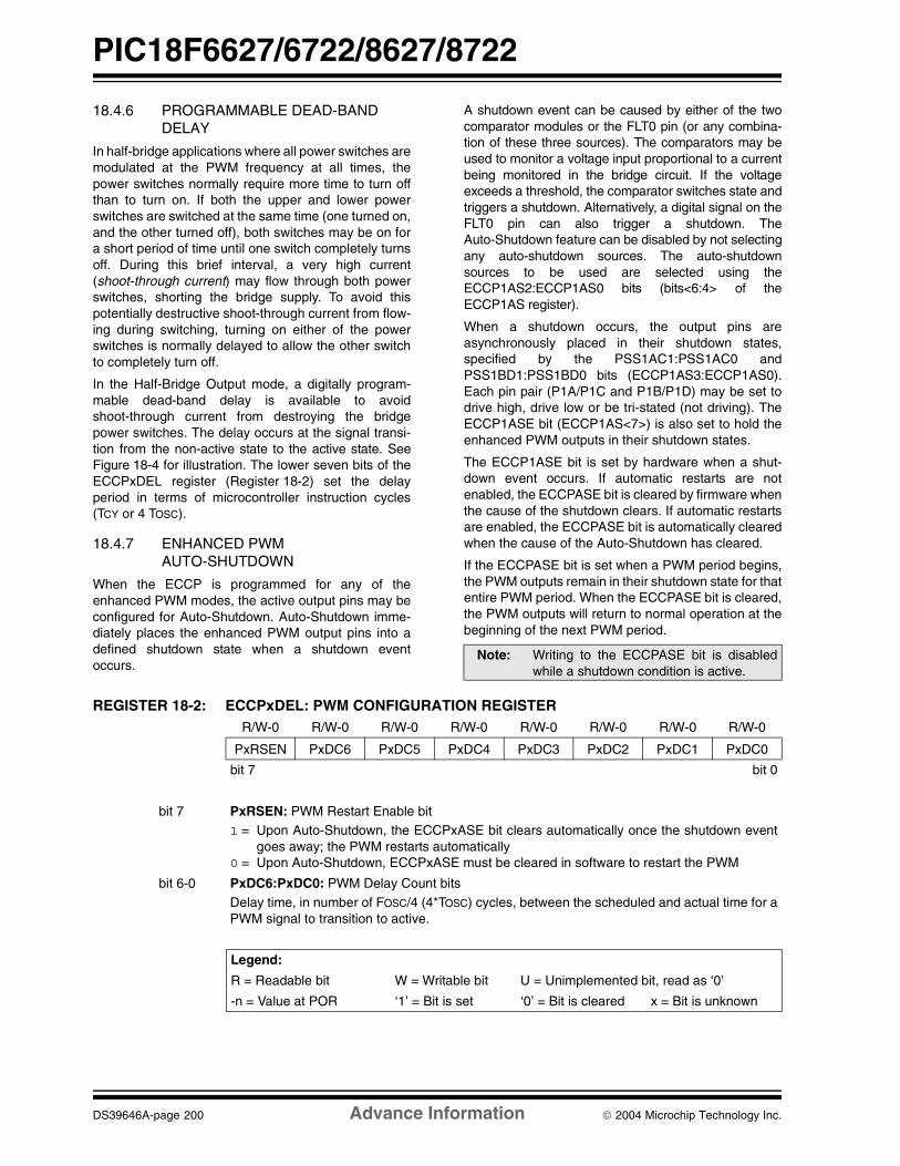
PIC18F6627/6722/8627/8722
DS39646A-page 200 Advance Information 2004 Microchip Technology Inc.
18.4.6 PROGRAMMABLE DEAD-BAND DELAY
In half-bridge applications where all power switches aremodulated at the PWM frequency at all times, thepower switches normally require more time to turn offthan to turn on. If both the upper and lower powerswitches are switched at the same time (one turned on,and the other turned off), both switches may be on fora short period of time until one switch completely turnsoff. During this brief interval, a very high current(shoot-through current) may flow through both powerswitches, shorting the bridge supply. To avoid thispotentially destructive shoot-through current from flow-ing during switching, turning on either of the powerswitches is normally delayed to allow the other switchto completely turn off.
In the Half-Bridge Output mode, a digitally program-mable dead-band delay is available to avoidshoot-through current from destroying the bridgepower switches. The delay occurs at the signal transi-tion from the non-active state to the active state. SeeFigure 18-4 for illustration. The lower seven bits of theECCPxDEL register (Register 18-2) set the delayperiod in terms of microcontroller instruction cycles(TCY or 4 TOSC).
18.4.7 ENHANCED PWM AUTO-SHUTDOWN
When the ECCP is programmed for any of theenhanced PWM modes, the active output pins may beconfigured for Auto-Shutdown. Auto-Shutdown imme-diately places the enhanced PWM output pins into adefined shutdown state when a shutdown eventoccurs.
A shutdown event can be caused by either of the twocomparator modules or the FLT0 pin (or any combina-tion of these three sources). The comparators may beused to monitor a voltage input proportional to a currentbeing monitored in the bridge circuit. If the voltageexceeds a threshold, the comparator switches state andtriggers a shutdown. Alternatively, a digital signal on theFLT0 pin can also trigger a shutdown. TheAuto-Shutdown feature can be disabled by not selectingany auto-shutdown sources. The auto-shutdownsources to be used are selected using theECCP1AS2:ECCP1AS0 bits (bits<6:4> of theECCP1AS register).
When a shutdown occurs, the output pins areasynchronously placed in their shutdown states,specified by the PSS1AC1:PSS1AC0 andPSS1BD1:PSS1BD0 bits (ECCP1AS3:ECCP1AS0).Each pin pair (P1A/P1C and P1B/P1D) may be set todrive high, drive low or be tri-stated (not driving). TheECCP1ASE bit (ECCP1AS<7>) is also set to hold theenhanced PWM outputs in their shutdown states.
The ECCP1ASE bit is set by hardware when a shut-down event occurs. If automatic restarts are notenabled, the ECCPASE bit is cleared by firmware whenthe cause of the shutdown clears. If automatic restartsare enabled, the ECCPASE bit is automatically clearedwhen the cause of the Auto-Shutdown has cleared.
If the ECCPASE bit is set when a PWM period begins,the PWM outputs remain in their shutdown state for thatentire PWM period. When the ECCPASE bit is cleared,the PWM outputs will return to normal operation at thebeginning of the next PWM period.
REGISTER 18-2: ECCPxDEL: PWM CONFIGURATION REGISTER
Note: Writing to the ECCPASE bit is disabledwhile a shutdown condition is active.
R/W-0 R/W-0 R/W-0 R/W-0 R/W-0 R/W-0 R/W-0 R/W-0
PxRSEN PxDC6 PxDC5 PxDC4 PxDC3 PxDC2 PxDC1 PxDC0
bit 7 bit 0
bit 7 PxRSEN: PWM Restart Enable bit1 = Upon Auto-Shutdown, the ECCPxASE bit clears automatically once the shutdown event
goes away; the PWM restarts automatically0 = Upon Auto-Shutdown, ECCPxASE must be cleared in software to restart the PWM
bit 6-0 PxDC6:PxDC0: PWM Delay Count bitsDelay time, in number of FOSC/4 (4*TOSC) cycles, between the scheduled and actual time for aPWM signal to transition to active.
Legend:
R = Readable bit W = Writable bit U = Unimplemented bit, read as ‘0’
-n = Value at POR ‘1’ = Bit is set ‘0’ = Bit is cleared x = Bit is unknown

2004 Microchip Technology Inc. Advance Information DS39646A-page 201
PIC18F6627/6722/8627/8722
REGISTER 18-3: ECCPxAS: ENHANCED CCP AUTO-SHUTDOWN CONTROL REGISTER R/W-0 R/W-0 R/W-0 R/W-0 R/W-0 R/W-0 R/W-0 R/W-0
ECCPxASE ECCPxAS2 ECCPxAS1 ECCPxAS0 PSSxAC1 PSSxAC0 PSSxBD1 PSSxBD0
bit 7 bit 0
bit 7 ECCPxASE: ECCP Auto-Shutdown Event Status bit0 = ECCP outputs are operating 1 = A shutdown event has occurred; ECCP outputs are in shutdown state
bit 6-4 ECCPxAS2:ECCPxAS0: ECCP Auto-Shutdown Source Select bits
000 = Auto-Shutdown is disabled001 = Comparator 1 output010 = Comparator 2 output011 = Either Comparator 1 or 2100 = FLT0101 = FLT0 or Comparator 1110 = FLT0 or Comparator 2111 = FLT0 or Comparator 1 or Comparator 2
bit 3-2 PSSxAC1:PSSxAC0: Pin A and C Shutdown State Control bits00 = Drive Pins A and C to ‘0’01 = Drive Pins A and C to ‘1’1x = Pins A and C tri-state
bit 1-0 PSSxBD1:PSSxBD0: Pin B and D Shutdown State Control bits
00 = Drive Pins B and D to ‘0’01 = Drive Pins B and D to ‘1’1x = Pins B and D tri-state
Legend:
R = Readable bit W = Writable bit U = Unimplemented bit, read as ‘0’
-n = Value at POR ‘1’ = Bit is set ‘0’ = Bit is cleared x = Bit is unknown

PIC18F6627/6722/8627/8722
DS39646A-page 202 Advance Information 2004 Microchip Technology Inc.
18.4.7.1 Auto-Shutdown and Automatic Restart
The Auto-Shutdown feature can be configured to allowautomatic restarts of the module following a shutdownevent. This is enabled by setting the P1RSEN bit of theECCP1DEL register (ECCP1DEL<7>).
In Shutdown mode with PRSEN = 1 (Figure 18-10), theECCPASE bit will remain set for as long as the causeof the shutdown continues. When the shutdown condi-tion clears, the ECCP1ASE bit is cleared. If PRSEN = 0(Figure 18-11), once a shutdown condition occurs, theECCP1ASE bit will remain set until it is cleared by firm-ware. Once ECCP1ASE is cleared, the enhancedPWM will resume at the beginning of the next PWMperiod.
Independent of the P1RSEN bit setting, if theauto-shutdown source is one of the comparators, theshutdown condition is a level. The ECCP1ASE bit can-not be cleared as long as the cause of the shutdownpersists.
The Auto-Shutdown mode can be forced by writing a ‘1’to the ECCPASE bit.
18.4.8 START-UP CONSIDERATIONS
When the ECCP module is used in the PWM mode, theapplication hardware must use the proper externalpull-up and/or pull-down resistors on the PWM outputpins. When the microcontroller is released from Reset,all of the I/O pins are in the high-impedance state. Theexternal circuits must keep the power switch devices inthe off state until the microcontroller drives the I/O pinswith the proper signal levels, or activates the PWMoutput(s).
The CCP1M1:CCP1M0 bits (CCP1CON<1:0>) allowthe user to choose whether the PWM output signals areactive-high or active-low for each pair of PWM outputpins (P1A/P1C and P1B/P1D). The PWM output polar-ities must be selected before the PWM pins are config-ured as outputs. Changing the polarity configurationwhile the PWM pins are configured as outputs is notrecommended since it may result in damage to theapplication circuits.
The P1A, P1B, P1C and P1D output latches may not bein the proper states when the PWM module is initialized.Enabling the PWM pins for output at the same time asthe ECCP module may cause damage to the applica-tion circuit. The ECCP module must be enabled in theproper output mode and complete a full PWM cyclebefore configuring the PWM pins as outputs. The com-pletion of a full PWM cycle is indicated by the TMR2IFbit being set as the second PWM period begins.
FIGURE 18-10: PWM AUTO -SHUTDOWN (PRSEN = 1, AUTO-RESTART ENABLED)
FIGURE 18-11: PWM AUTO -SHUTDOWN (PRSEN = 0, AUTO-RESTART DISABLED)
Note: Writing to the ECCPASE bit is disabledwhile a shutdown condition is active.
Shutdown
PWM
ECCPASE bit
Activity
Event
ShutdownEvent Occurs
ShutdownEvent Clears
PWMResumes
Normal PWM
Start ofPWM Period
PWM Period
Shutdown
PWM
ECCPASE bit
Activity
Event
ShutdownEvent Occurs
ShutdownEvent Clears
PWMResumes
Normal PWM
Start ofPWM Period
ECCPASECleared byFirmware
PWM Period

2004 Microchip Technology Inc. Advance Information DS39646A-page 203
PIC18F6627/6722/8627/8722
18.4.9 SETUP FOR PWM OPERATION
The following steps should be taken when configuringthe ECCP1 module for PWM operation using Timer2:
1. Configure the PWM pins, P1A and P1B (andP1C and P1D, if used), as inputs by setting thecorresponding TRIS bits.
2. Set the PWM period by loading the PR2 register.3. If Auto-Shutdown is required do the following:
• Disable Auto-Shutdown (ECCP1AS = 0)
• Configure source (FLT0, Comparator 1 or Comparator 2)
• Wait for non-shutdown condition4. Configure the ECCP module for the desired
PWM mode and configuration by loading theCCP1CON register with the appropriate values:
• Select one of the available output configurations and direction with the P1M1:P1M0 bits.
• Select the polarities of the PWM output signals with the CCP1M3:CCP1M0 bits.
5. Set the PWM duty cycle by loading the CCPR1Lregister and CCP1CON<5:4> bits.
6. For Half-Bridge Output mode, set thedead-band delay by loading PWM1CON<6:0>with the appropriate value.
7. If auto-shutdown operation is required, load theECCP1AS register:• Select the auto-shutdown sources using the
ECCPAS2:ECCPAS0 bits.• Select the shutdown states of the PWM
output pins using the PSSAC1:PSSAC0 and PSSBD1:PSSBD0 bits.
• Set the ECCPASE bit (ECCP1AS<7>).• Configure the comparators using the CMCON
register.• Configure the comparator inputs as analog
inputs.8. If auto-restart operation is required, set the
PRSEN bit (PWM1CON<7>).9. Configure and start TMR2:
• Clear the TMR2 interrupt flag bit by clearing the TMR2IF bit (PIR1<1>).
• Set the TMR2 prescale value by loading the T2CKPS bits (T2CON<1:0>).
• Enable Timer2 by setting the TMR2ON bit (T2CON<2>).
10. Enable PWM outputs after a new PWM cyclehas started:• Wait until TMRn overflows (TMRnIF bit is set).
• Enable the CCP1/P1A, P1B, P1C and/or P1D pin outputs by clearing the respective TRIS bits.
• Clear the ECCPASE bit (ECCP1AS<7>).
18.4.10 OPERATION IN POWER-MANAGED MODES
In Sleep mode, all clock sources are disabled. Timer2will not increment and the state of the module will notchange. If the ECCP pin is driving a value, it will continueto drive that value. When the device wakes up, it willcontinue from this state. If Two-Speed Start-ups areenabled, the initial start-up frequency from INTOSC andthe postscaler may not be stable immediately.
In PRI_IDLE mode, the primary clock will continue toclock the ECCP module without change. In all otherpower-managed modes, the selected power-managedmode clock will clock Timer2. Other power-managedmode clocks will most likely be different than theprimary clock frequency.
18.4.10.1 Operation with Fail-Safe Clock Monitor
If the Fail-Safe Clock Monitor is enabled, a clock failurewill force the device into the power-managed RC_RUNmode and the OSCFIF bit (PIR2<7>) will be set. TheECCP will then be clocked from the internal oscillatorclock source, which may have a different clockfrequency than the primary clock.
See the previous section for additional details.
18.4.11 EFFECTS OF A RESET
Both Power-on Reset and subsequent Resets will forceall ports to Input mode and the CCP registers to theirReset states.
This forces the enhanced CCP module to reset to astate compatible with the standard CCP module.

PIC18F6627/6722/8627/8722
DS39646A-page 204 Advance Information 2004 Microchip Technology Inc.
TABLE 18-5: REGISTERS ASSOCIATED WITH ECCP MODULES AND TIMER1 TO TIMER4
Name Bit 7 Bit 6 Bit 5 Bit 4 Bit 3 Bit 2 Bit 1 Bit 0Reset Values
on page
INTCON GIE/GIEH PEIE/GIEL TMR0IE INT0IE RBIE TMR0IF INT0IF RBIF 57
RCON IPEN SBOREN — RI TO PD POR BOR 58
PIR1 PSPIF ADIF RC1IF TX1IF SSP1IF CCP1IF TMR2IF TMR1IF 60
PIE1 PSPIE ADIE RC1IE TX1IE SSP1IE CCP1IE TMR2IE TMR1IE 60
IPR1 PSPIP ADIP RC1IP TX1IP SSP1IP CCP1IP TMR2IP TMR1IP 60
PIR2 OSCFIF CMIF — EEIF BCL1IF HLVDIF TMR3IF CCP2IF 60
PIE2 OSCFIE CMIE — EEIE BCL1IE HLVDIE TMR3IE CCP2IE 60
IPR2 OSCFIP CMIP — EEIP BCL1IP HLVDIP TMR3IP CCP2IP 60
PIR3 SSP2IF BCL2IF RC2IF TX2IF TMR4IF CCP5IF CCP4IF CCP3IF 60
PIE3 SSP2IE BCL2IE RC2IE TX2IE TMR4IE CCP5IE CCP4IE CCP3IE 60
IPR3 SSP2IP BCL2IP RC2IP TX2IP TMR4IP CCP5IP CCP4IP CCP3IP 60
TRISB PORTB Data Direction Register 60
TRISC PORTC Data Direction Register 60
TRISE PORTE Data Direction Register 60
TRISG — — — PORTG Data Direction Register 60
TRISH PORTH Data Direction Register(1) 60
TMR1L Holding Register for the Least Significant Byte of the 16-bit TMR1 Register 58
TMR1H Holding Register for the Most Significant Byte of the 16-bit TMR1 Register 58
T1CON RD16 T1RUN T1CKPS1 T1CKPS0 T1OSCEN T1SYNC TMR1CS TMR1ON 58
TMR2 Timer2 Module Register 58
T2CON — T2OUTPS3 T2OUTPS2 T2OUTPS1 T2OUTPS0 TMR2ON T2CKPS1 T2CKPS0 58
PR2 Timer2 Period Register 58
TMR3L Holding Register for the Least Significant Byte of the 16-bit TMR3 Register 59
TMR3H Holding Register for the Most Significant Byte of the 16-bit TMR3 Register 59
T3CON RD16 T3CCP2 T3CKPS1 T3CKPS0 T3CCP1 T3SYNC TMR3CS TMR3ON 59
TMR4 Timer4 Module Register 61
T4CON — T4OUTPS3 T4OUTPS2 T4OUTPS1 T4OUTPS0 TMR4ON T4CKPS1 T4CKPS0 61
PR4 Timer4 Period Register 61
CCPRxL(1) Capture/Compare/PWM Register x (LSB) 59, 61
CCPRxH(1) Capture/Compare/PWM Register x (MSB) 59, 61
ECCPxCON(1) PxM1 PxM0 DCxB1 DCxB0 CCPxM3 CCPxM2 CCPxM1 CCPxM0 59
ECCPxAS(1) ECCPxASE ECCPxAS2 ECCPxAS1 ECCPxAS0 PSSxAC1 PSSxAC0 PSSxBD1 PSSxBD0 59, 61
ECCPxDEL(1) PxRSEN PxDC6 PxDC5 PxDC4 PxDC3 PxDC2 PxDC1 PxDC0 61
Legend: x = unknown, u = unchanged, – = unimplemented, read as ‘0’. Shaded cells are not used during ECCP operation.Note 1: Generic term for all of the identical registers of this name for all enhanced CCP modules, where ‘x’ identifies the
individual module (ECCP1, ECCP2 or ECCP3). Bit assignments and Reset values for all registers of the same generic name are identical.

2004 Microchip Technology Inc. Advance Information DS39646A-page 205
PIC18F6627/6722/8627/8722
19.0 MASTER SYNCHRONOUS SERIAL PORT (MSSP) MODULE
19.1 Master SSP (MSSP) Module Overview
The Master Synchronous Serial Port (MSSP) module isa serial interface, useful for communicating with otherperipheral or microcontroller devices. These peripheraldevices may be serial EEPROMs, shift registers, dis-play drivers, A/D converters, etc. The MSSP modulecan operate in one of two modes:
• Serial Peripheral Interface (SPI)• Inter-Integrated Circuit (I2C)
- Full Master mode- Slave mode (with general address call)
The I2C interface supports the following modes inhardware:
• Master mode• Multi-Master mode• Slave mode
All members of the PIC18F6627/6722/8627/8722family have two MSSP modules, designated as MSSP1and MSSP2. Each module operates independently ofthe other.
19.2 Control Registers
Each MSSP module has three associated control reg-isters. These include a status register (SSPxSTAT) andtwo control registers (SSPxCON1 and SSPxCON2).The use of these registers and their individual configu-ration bits differ significantly depending on whether theMSSP module is operated in SPI or I2C mode.
Additional details are provided under the individualsections.
19.3 SPI Mode
The SPI mode allows 8 bits of data to be synchronouslytransmitted and received simultaneously. All fourmodes of SPI are supported. To accomplishcommunication, typically three pins are used:
• Serial Data Out (SDOx) – RC5/SDO1 or RD4/SDO2
• Serial Data In (SDIx) – RC4/SDI1/SDA1 or RD5/SDI2/SDA2
• Serial Clock (SCKx) – RC3/SCK1/SCL1 or RD6/SCK2/SCL2
Additionally, a fourth pin may be used when in a Slavemode of operation:
• Slave Select (SSx) – RF7/SS1 or RD7/SS2
Figure 19-1 shows the block diagram of the MSSPmodule when operating in SPI mode.
FIGURE 19-1: MSSP BLOCK DIAGRAM (SPI™ MODE)
Note: Throughout this section, generic referer-ences to an MSSP module in any of itsoperating modes may be interpreted asbeing equally applicable to MSSP1 orMSSP2. Register names and module I/Osignals use the generic designator ‘x’ toindicate the use of a numeral to distingusiha particular module, when required. Con-trol bit names are not individuated.
Note: In devices with more than one MSSPmodule, it is very important to pay closeattention to SSPCON register names.SSP1CON1 and SSP1CON2 controldifferent operational aspects of the samemodule, while SSP1CON1 andSSP2CON1 control the same features fortwo different modules.
( )
Read Write
InternalData Bus
SSPxSR reg
SSPM3:SSPM0
bit 0 ShiftClock
SS ControlEnable
EdgeSelect
Clock Select
TMR2 Output
TOSCPrescaler4, 16, 64
2EdgeSelect
2
4
Data to TXx/RXx in SSPxSRTRIS bit
2SMP:CKE
RC5 or RD4
SSPxBUF reg
RC4 or RD5
RF7 or RD7
RC3 or RD6
Note: Only port I/O names are used in this diagramfor the sake of brevity. Refer to the text for a fulllisted of multiplexed functions.

PIC18F6627/6722/8627/8722
DS39646A-page 206 Advance Information 2004 Microchip Technology Inc.
19.3.1 REGISTERS
Each MSSP module has four registers for SPI modeoperation. These are:
• MSSP Control Register 1 (SSPxCON1)• MSSP Status Register (SSPxSTAT)
• Serial Receive/Transmit Buffer Register (SSPxBUF)
• MSSP Shift Register (SSPxSR) – Not directly accessible
SSPxCON1 and SSPxSTAT are the control and statusregisters in SPI mode operation. The SSPxCON1register is readable and writable. The lower 6 bits ofthe SSPxSTAT are read-only. The upper two bits of theSSPxSTAT are read/write.
SSPxSR is the shift register used for shifting data in orout. SSPxBUF is the buffer register to which databytes are written to or read from.
In receive operations, SSPxSR and SSPxBUFtogether create a double-buffered receiver. WhenSSPxSR receives a complete byte, it is transferred toSSPxBUF and the SSPxIF interrupt is set.
During transmission, the SSPxBUF is notdouble-buffered. A write to SSPxBUF will write to bothSSPxBUF and SSPxSR.
REGISTER 19-1: SSPxSTAT: MSSPx STATUS REGISTER (SPI™ MODE)
R/W-0 R/W-0 R-0 R-0 R-0 R-0 R-0 R-0
SMP CKE D/A P S R/W UA BF
bit 7 bit 0
bit 7 SMP: Sample bitSPI Master mode:1 = Input data sampled at end of data output time0 = Input data sampled at middle of data output time
SPI Slave mode:SMP must be cleared when SPI is used in Slave mode.
bit 6 CKE: SPI Clock Select bit1 = Transmit occurs on transition from active to Idle clock state0 = Transmit occurs on transition from Idle to Active clock state
Note: Polarity of clock state is set by the CKP bit (SSPxCON1<4>).
bit 5 D/A: Data/Address bit Used in I2C mode only.
bit 4 P: Stop bit Used in I2C mode only. This bit is cleared when the MSSP module is disabled, SSPEN is cleared.
bit 3 S: Start bit
Used in I2C mode only.
bit 2 R/W: Read/Write Information bit
Used in I2C mode only.
bit 1 UA: Update Address bit
Used in I2C mode only.
bit 0 BF: Buffer Full Status bit (Receive mode only)
1 = Receive complete, SSPxBUF is full 0 = Receive not complete, SSPxBUF is empty
Legend:
R = Readable bit W = Writable bit U = Unimplemented bit, read as ‘0’
-n = Value at POR ‘1’ = Bit is set ‘0’ = Bit is cleared x = Bit is unknown
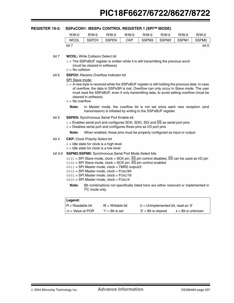
2004 Microchip Technology Inc. Advance Information DS39646A-page 207
PIC18F6627/6722/8627/8722
REGISTER 19-2: SSPxCON1: MSSPx CONTROL REGISTER 1 (SPI™ MODE)
R/W-0 R/W-0 R/W-0 R/W-0 R/W-0 R/W-0 R/W-0 R/W-0
WCOL SSPOV SSPEN CKP SSPM3 SSPM2 SSPM1 SSPM0
bit 7 bit 0
bit 7 WCOL: Write Collision Detect bit1 = The SSPxBUF register is written while it is still transmitting the previous word
(must be cleared in software) 0 = No collision
bit 6 SSPOV: Receive Overflow Indicator bit SPI Slave mode: 1 = A new byte is received while the SSPxBUF register is still holding the previous data. In case
of overflow, the data in SSPxSR is lost. Overflow can only occur in Slave mode. The usermust read the SSPxBUF, even if only transmitting data, to avoid setting overflow (must becleared in software).
0 = No overflow
Note: In Master mode, the overflow bit is not set since each new reception (andtransmission) is initiated by writing to the SSPxBUF register.
bit 5 SSPEN: Synchronous Serial Port Enable bit 1 = Enables serial port and configures SCK, SDO, SDI and SS as serial port pins 0 = Disables serial port and configures these pins as I/O port pins
Note: When enabled, these pins must be properly configured as input or output.
bit 4 CKP: Clock Polarity Select bit 1 = Idle state for clock is a high level 0 = Idle state for clock is a low level
bit 3-0 SSPM3:SSPM0: Synchronous Serial Port Mode Select bits
0101 = SPI Slave mode, clock = SCK pin, SS pin control disabled, SS can be used as I/O pin 0100 = SPI Slave mode, clock = SCK pin, SS pin control enabled0011 = SPI Master mode, clock = TMR2 output/2 0010 = SPI Master mode, clock = FOSC/64 0001 = SPI Master mode, clock = FOSC/16 0000 = SPI Master mode, clock = FOSC/4
Note: Bit combinations not specifically listed here are either reserved or implemented inI2C mode only.
Legend:
R = Readable bit W = Writable bit U = Unimplemented bit, read as ‘0’
-n = Value at POR ‘1’ = Bit is set ‘0’ = Bit is cleared x = Bit is unknown

PIC18F6627/6722/8627/8722
DS39646A-page 208 Advance Information 2004 Microchip Technology Inc.
19.3.2 OPERATION
When initializing the SPI, several options need to bespecified. This is done by programming the appropriatecontrol bits (SSPxCON1<5:0> and SSPxSTAT<7:6>).These control bits allow the following to be specified:
• Master mode (SCK is the clock output)
• Slave mode (SCK is the clock input)• Clock Polarity (Idle state of SCK)• Data Input Sample Phase (middle or end of data
output time)• Clock Edge (output data on rising/falling edge of
SCK)• Clock Rate (Master mode only)
• Slave Select mode (Slave mode only)
Each MSSP consists of a transmit/receive shift register(SSPxSR) and a buffer register (SSPxBUF). TheSSPxSR shifts the data in and out of the device, MSbfirst. The SSPxBUF holds the data that was written tothe SSPxSR until the received data is ready. Once the8 bits of data have been received, that byte is moved tothe SSPxBUF register. Then, the Buffer Full detect bit,BF (SSPxSTAT<0>), and the interrupt flag bit, SSPxIF,are set. This double-buffering of the received data(SSPxBUF) allows the next byte to start reception
before reading the data that was just received. Anywrite to the SSPxBUF register during transmis-sion/reception of data will be ignored and the WriteCollision Detect bit, WCOL (SSPxCON1<7>), will beset. User software must clear the WCOL bit so that itcan be determined if the following write(s) to theSSPxBUF register completed successfully.
When the application software is expecting to receivevalid data, the SSPxBUF should be read before thenext byte of data to transfer is written to the SSPxBUF.The Buffer Full bit, BF (SSPxSTAT<0>), indicates whenSSPxBUF has been loaded with the received data(transmission is complete). When the SSPxBUF isread, the BF bit is cleared. This data may be irrelevantif the SPI is only a transmitter. Generally, the MSSPinterrupt is used to determine when the transmis-sion/reception has completed. If the interrupt method isnot going to be used, then software polling can be doneto ensure that a write collision does not occur.Example 19-1 shows the loading of the SSP1BUF(SSP1SR) for data transmission.
The SSPxSR is not directly readable or writable andcan only be accessed by addressing the SSPxBUFregister. Additionally, the SSPxSTAT register indicatesthe various status conditions.
EXAMPLE 19-1: LOADING THE SSP1BUF (SSP1SR) REGISTER LOOP BTFSS SSP1STAT, BF ;Has data been received (transmit complete)?
BRA LOOP ;No MOVF SSP1BUF, W ;WREG reg = contents of SSP1BUF
MOVWF RXDATA ;Save in user RAM, if data is meaningful
MOVF TXDATA, W ;W reg = contents of TXDATA MOVWF SSP1BUF ;New data to xmit

2004 Microchip Technology Inc. Advance Information DS39646A-page 209
PIC18F6627/6722/8627/8722
19.3.3 ENABLING SPI I/O
To enable the serial port, SSP Enable bit, SSPEN(SSPxCON1<5>), must be set. To reset or reconfigureSPI mode, clear the SSPEN bit, reinitialize theSSPxCON registers and then set the SSPEN bit. Thisconfigures the SDIx, SDOx, SCKx and SSx pins asserial port pins. For the pins to behave as the serial portfunction, some must have their data direction bits (inthe TRIS register) appropriately programmed asfollows:
• SDI is automatically controlled by the SPI module • SDO must have TRISC<5> bit cleared• SCK (Master mode) must have TRISC<3> bit
cleared• SCK (Slave mode) must have TRISC<3> bit set
• SS must have TRISA<5> bit set
Any serial port function that is not desired may beoverridden by programming the corresponding datadirection (TRIS) register to the opposite value.
19.3.4 TYPICAL CONNECTION
Figure 19-2 shows a typical connection between twomicrocontrollers. The master controller (Processor 1)initiates the data transfer by sending the SCK signal.Data is shifted out of both shift registers on their pro-grammed clock edge and latched on the opposite edgeof the clock. Both processors should be programmed tothe same Clock Polarity (CKP), then both controllerswould send and receive data at the same time.Whether the data is meaningful (or dummy data)depends on the application software. This leads tothree scenarios for data transmission:
• Master sends data – Slave sends dummy data• Master sends data – Slave sends data
• Master sends dummy data – Slave sends data
FIGURE 19-2: SPI™ MASTER/SLAVE CONNECTION
Serial Input Buffer(SSPxBUF)
Shift Register(SSPxSR)
MSb LSb
SDO
SDI
PROCESSOR 1
SCK
SPI™ Master SSPM3:SSPM0 = 00xxb
Serial Input Buffer(SSPxBUF)
Shift Register(SSPxSR)
LSbMSb
SDI
SDO
PROCESSOR 2
SCK
SPI™ Slave SSPM3:SSPM0 = 010xb
Serial Clock

PIC18F6627/6722/8627/8722
DS39646A-page 210 Advance Information 2004 Microchip Technology Inc.
19.3.5 MASTER MODE
The master can initiate the data transfer at any timebecause it controls the SCK. The master determineswhen the slave (Processor 1, Figure 19-2) is tobroadcast data by the software protocol.
In Master mode, the data is transmitted/received assoon as the SSPxBUF register is written to. If the SPIis only going to receive, the SDO output could be dis-abled (programmed as an input). The SSPxSR registerwill continue to shift in the signal present on the SDI pinat the programmed clock rate. As each byte isreceived, it will be loaded into the SSPxBUF register asif a normal received byte (interrupts and status bitsappropriately set). This could be useful in receiverapplications as a “Line Activity Monitor” mode.
The clock polarity is selected by appropriatelyprogramming the CKP bit (SSPxCON1<4>). This then,would give waveforms for SPI communication asshown in Figure 19-3, Figure 19-5 and Figure 19-6,where the MSB is transmitted first. In Master mode, theSPI clock rate (bit rate) is user programmable to be oneof the following:
• FOSC/4 (or TCY)• FOSC/16 (or 4 • TCY)
• FOSC/64 (or 16 • TCY)• Timer2 output/2
This allows a maximum data rate (at 40 MHz) of10.00 Mbps.
Figure 19-3 shows the waveforms for Master mode.When the CKE bit is set, the SDOx data is valid beforethere is a clock edge on SCKx. The change of the inputsample is shown based on the state of the SMP bit. Thetime when the SSPxBUF is loaded with the receiveddata is shown.
FIGURE 19-3: SPI™ MODE WAVEFORM (MASTER MODE)
SCKx(CKP = 0
SCKx(CKP = 1
SCKx(CKP = 0
SCKx(CKP = 1
4 ClockModes
InputSample
InputSample
SDIx
bit 7 bit 0
SDOx bit 7 bit 6 bit 5 bit 4 bit 3 bit 2 bit 1 bit 0
bit 7
SDIx
SSPxIF
(SMP = 1)
(SMP = 0)
(SMP = 1)
CKE = 1)
CKE = 0)
CKE = 1)
CKE = 0)
(SMP = 0)
Write toSSPxBUF
SSPxSR toSSPxBUF
SDOx bit 7 bit 6 bit 5 bit 4 bit 3 bit 2 bit 1 bit 0
(CKE = 0)
(CKE = 1)
Next Q4 Cycleafter Q2↓
bit 0

2004 Microchip Technology Inc. Advance Information DS39646A-page 211
PIC18F6627/6722/8627/8722
19.3.6 SLAVE MODE
In Slave mode, the data is transmitted and received asthe external clock pulses appear on SCKx. When thelast bit is latched, the SSPxIF interrupt flag bit is set.
While in Slave mode, the external clock is supplied bythe external clock source on the SCKx pin. This exter-nal clock must meet the minimum high and low timesas specified in the electrical specifications.
While in Sleep mode, the slave can transmit/receivedata. When a byte is received, the device can be con-figured to wake-up from Sleep.
19.3.7 SLAVE SELECT SYNCHRONIZATION
The SSx pin allows a Synchronous Slave mode. TheSPI must be in Slave mode with the SSx pin controlenabled (SSPxCON1<3:0> = 04h). When the SSx pinis low, transmission and reception are enabled and theSDOx pin is driven. When the SSx pin goes high, theSDOx pin is no longer driven, even if in the middle of a
transmitted byte and becomes a floating output. Exter-nal pull-up/pull-down resistors may be desirabledepending on the application.
When the SPI module resets, the bit counter is forcedto ‘0’. This can be done by either forcing the SSx pin toa high level or clearing the SSPEN bit.
To emulate two-wire communication, the SDOx pin canbe connected to the SDIx pin. When the SPI needs tooperate as a receiver, the SDOx pin can be configuredas an input. This disables transmissions from theSDOx. The SDIx can always be left as an input (SDIfunction) since it cannot create a bus conflict.
FIGURE 19-4: SLAVE SYNCHRONIZATION WAVEFORM
Note 1: When the SPI is in Slave mode with SSxpin control enabled (SSPxCON1<3:0> =0100), the SPI module will reset if the SSxpin is set to VDD.
2: If the SPI is used in Slave mode with CKEset, then the SSx pin control must beenabled.
SCKx(CKP = 1
SCKx(CKP = 0
InputSample
SDIx
bit 7
SDOx bit 7 bit 6 bit 7
SSPxIFInterrupt
(SMP = 0)
CKE = 0)
CKE = 0)
(SMP = 0)
Write toSSPxBUF
SSPxSR toSSPxBUF
SSx
Flag
bit 0
bit 7
bit 0
Next Q4 Cycleafter Q2↓

PIC18F6627/6722/8627/8722
DS39646A-page 212 Advance Information 2004 Microchip Technology Inc.
FIGURE 19-5: SPI™ MODE WAVEFORM (SLAVE MODE WITH CKE = 0)
FIGURE 19-6: SPI™ MODE WAVEFORM (SLAVE MODE WITH CKE = 1)
SCKx(CKP = 1
SCKx(CKP = 0
InputSample
SDIx
bit 7
SDOx bit 7 bit 6 bit 5 bit 4 bit 3 bit 2 bit 1 bit 0
SSPxIFInterrupt
(SMP = 0)
CKE = 0)
CKE = 0)
(SMP = 0)
Write toSSPxBUF
SSPxSR toSSPxBUF
SSx
Flag
Optional
Next Q4 Cycleafter Q2↓
bit 0
SCKx(CKP = 1
SCKx(CKP = 0
InputSample
SDIx
bit 7 bit 0
SDOx bit 7 bit 6 bit 5 bit 4 bit 3 bit 2 bit 1 bit 0
SSPxIFInterrupt
(SMP = 0)
CKE = 1)
CKE = 1)
(SMP = 0)
Write toSSPxBUF
SSPxSR toSSPxBUF
SSx
Flag
Not Optional
Next Q4 Cycleafter Q2↓

2004 Microchip Technology Inc. Advance Information DS39646A-page 213
PIC18F6627/6722/8627/8722
19.3.8 OPERATION IN POWER-MANAGED MODES
In SPI Master mode, module clocks may be operatingat a different speed than when in full power mode; inthe case of the Sleep mode, all clocks are halted.
In idle modes, a clock is provided to the peripherals.That clock can be from the primary clock source, thesecondary clock (Timer1 oscillator) or the INTOSCsource. See Section 2.7 “Clock Sources and Oscil-lator Switching” for additional information.
In most cases, the speed that the master clocks SPIdata is not important; however, this should beevaluated for each system.
If MSSP interrupts are enabled, they can wake the con-troller from Sleep mode, or one of the Idle modes, whenthe master completes sending data. If an exit fromSleep or Idle mode is not desired, MSSP interruptsshould be disabled.
If the Sleep mode is selected, all module clocks arehalted and the transmission/reception will remain inthat state until the devices wakes. After the devicereturns to Run mode, the module will resumetransmitting and receiving data.
In SPI Slave mode, the SPI Transmit/Receive Shiftregister operates asynchronously to the device. Thisallows the device to be placed in any power-managedmode and data to be shifted into the SPI Trans-mit/Receive Shift register. When all 8 bits have beenreceived, the MSSP interrupt flag bit will be set and ifenabled, will wake the device.
19.3.9 EFFECTS OF A RESET
A Reset disables the MSSP module and terminates thecurrent transfer.
19.3.10 BUS MODE COMPATIBILITY
Table 19-1 shows the compatibility between thestandard SPI modes and the states of the CKP andCKE control bits.
TABLE 19-1: SPI™ BUS MODES
There is also an SMP bit which controls when the datais sampled.
19.3.11 SPI CLOCK SPEED AND MODULE INTERACTIONS
Because MSSP1 and MSSP2 are independent mod-ules, they can operate simultaneously at different datarates. Setting the SSPM3:SSPM0 bits of the SSPxCONregister determines the rate for the corresponding mod-ule.
An exception is when both modules use Timer2 as atime base in Master mode. In this instance, anychanges to Timer2’s operation will affect both MSSPmodules equally. If different bit rates are required foreach module, the user should select one of the otherthree time base options for one of the modules.
Standard SPI™ Mode Terminology
Control Bits State
CKP CKE
0, 0 0 1
0, 1 0 0
1, 0 1 1
1, 1 1 0

PIC18F6627/6722/8627/8722
DS39646A-page 214 Advance Information 2004 Microchip Technology Inc.
TABLE 19-2: REGISTERS ASSOCIATED WITH SPI OPERATION
Name Bit 7 Bit 6 Bit 5 Bit 4 Bit 3 Bit 2 Bit 1 Bit 0Reset Values
on page
INTCON GIE/GIEH PEIE/GIEL TMR0IE INT0IE RBIE TMR0IF INT0IF RBIF 57
PIR1 PSPIF ADIF RC1IF TX1IF SSP1IF CCP1IF TMR2IF TMR1IF 60
PIE1 PSPIE ADIE RC1IE TX1IE SSP1IE CCP1IE TMR2IE TMR1IE 60
IPR1 PSPIP ADIP RC1IP TX1IP SSP1IP CCP1IP TMR2IP TMR1IP 60
PIR3 SSP2IF BCL2IF RC2IF TX2IF TMR4IF CCP5IF CCP4IF CCP3IF 60
PIE3 SSP2IE BCL2IE RC2IE TX2IE TMR4IE CCP5IE CCP4IE CCP3IE 60
IPR3 SSP2IP BCL2IP RC2IP TX2IP TMR4IP CCP5IP CCP4IP CCP3IP 60
TRISC PORTC Data Direction Control Register 60
TRISD PORTD Data Direction Control Register 60
TRISF PORTF Data Direction Control Register 60
TRISJ PORTJ Data Direction Control Register 60
TMR2 Timer2 Register 58
PR2 Timer2 Period Register 58
SSP1BUF MSSP1 Receive Buffer/Transmit Register 58
SSP1CON1 WCOL SSPOV SSPEN CKP SSPM3 SSPM2 SSPM1 SSPM0 58
SSP1STAT SMP CKE D/A P S R/W UA BF 58
SSP2BUF MSSP2 Receive Buffer/Transmit Register 61
SSP2CON1 WCOL SSPOV SSPEN CKP SSPM3 SSPM2 SSPM1 SSPM0 61
SSP2STAT SMP CKE D/A P S R/W UA BF 61
Legend: Shaded cells are not used by the MSSP in SPI mode.Note 1: PORTA<7:6> and their direction bits are individually configured as port pins based on various primary
oscillator modes. When disabled, these bits read as ‘0’.

2004 Microchip Technology Inc. Advance Information DS39646A-page 215
PIC18F6627/6722/8627/8722
19.4 I2C Mode
The MSSP module in I2C mode fully implements allmaster and slave functions (including general callsupport) and provides interrupts on Start and Stop bitsin hardware to determine a free bus (multi-masterfunction). The MSSP module implements the standardmode specifications, as well as 7-bit and 10-bitaddressing.
Two pins are used for data transfer:
• Serial clock (SCLx) – RC3/SCK1/SCL1 or RD6/SCK2/SCL2
• Serial data (SDAx) – RC4/SDI1/SDA1 or RD5/SDI2/SDA2
The user must configure these pins as inputs by settingthe TRISC<4:3> bits.
FIGURE 19-7: MSSP BLOCK DIAGRAM (I2C™ MODE)
19.4.1 REGISTERS
The MSSP module has six registers for I2C operation.These are:
• MSSP Control Register 1 (SSPxCON1)
• MSSP Control Register 2 (SSPxCON2)• MSSP Status Register (SSPxSTAT)• Serial Receive/Transmit Buffer Register
(SSPxBUF)• MSSP Shift Register (SSPxSR) – Not directly
accessible• MSSP Address Register (SSPxADD)
SSPxCON1, SSPxCON2 and SSPxSTAT are the con-trol and status registers in I2C mode operation. TheSSPxCON1 and SSPxCON2 registers are readable andwritable. The lower 6 bits of the SSPxSTAT areread-only. The upper two bits of the SSPxSTAT areread/write.
SSPxSR is the shift register used for shifting data in orout. SSPxBUF is the buffer register to which databytes are written to or read from.
SSPxADD register holds the slave device addresswhen the SSP is configured in I2C Slave mode. Whenthe SSP is configured in Master mode, the lower sevenbits of SSPxADD act as the Baud Rate Generatorreload value.
In receive operations, SSPxSR and SSPxBUFtogether create a double-buffered receiver. WhenSSPxSR receives a complete byte, it is transferred toSSPxBUF and the SSPxIF interrupt is set.
During transmission, the SSPxBUF is notdouble-buffered. A write to SSPxBUF will write to bothSSPxBUF and SSPxSR.
Read Write
SSPxSR reg
Match Detect
SSPxADD reg
Start andStop bit Detect
SSPxBUF reg
InternalData Bus
Addr Match
Set, ResetS, P bits
(SSPxSTAT reg)
RC3 or RD6
RC4 or RD5
ShiftClock
MSb LSb
Note: Only port I/O names are used in this diagramfor the sake of brevity. Refer to the text for a fulllisted of multiplexed functions.

PIC18F6627/6722/8627/8722
DS39646A-page 216 Advance Information 2004 Microchip Technology Inc.
REGISTER 19-3: SSPxSTAT: MSSPx STATUS REGISTER (I2C™ MODE)
R/W-0 R/W-0 R-0 R-0 R-0 R-0 R-0 R-0
SMP CKE D/A P S R/W UA BF
bit 7 bit 0
bit 7 SMP: Slew Rate Control bitIn Master or Slave mode: 1 = Slew rate control disabled for Standard Speed mode (100 kHz and 1 MHz) 0 = Slew rate control enabled for High-Speed mode (400 kHz)
bit 6 CKE: SMBus Select bitIn Master or Slave mode:1 = Enable SMBus specific inputs 0 = Disable SMBus specific inputs
bit 5 D/A: Data/Address bit In Master mode:Reserved.In Slave mode:1 = Indicates that the last byte received or transmitted was data0 = Indicates that the last byte received or transmitted was address
bit 4 P: Stop bit1 = Indicates that a Stop bit has been detected last0 = Stop bit was not detected last
Note: This bit is cleared on Reset and when SSPEN is cleared.
bit 3 S: Start bit1 = Indicates that a Start bit has been detected last0 = Start bit was not detected last
Note: This bit is cleared on Reset and when SSPEN is cleared.
bit 2 R/W: Read/Write Information bit (I2C mode only)In Slave mode:1 = Read0 = Write
Note: This bit holds the R/W bit information following the last address match. This bit isonly valid from the address match to the next Start bit, Stop bit or not ACK bit.
In Master mode:1 = Transmit is in progress0 = Transmit is not in progress
Note: ORing this bit with SEN, RSEN, PEN, RCEN or ACKEN will indicate if the MSSP isin Active mode.
bit 1 UA: Update Address bit (10-bit Slave mode only)
1 = Indicates that the user needs to update the address in the SSPxADD register 0 = Address does not need to be updated
bit 0 BF: Buffer Full Status bitIn Transmit mode: 1 = SSPxBUF is full 0 = SSPxBUF is emptyIn Receive mode:1 = SSPxBUF is full (does not include the ACK and Stop bits)0 = SSPxBUF is empty (does not include the ACK and Stop bits)
Legend:
R = Readable bit W = Writable bit U = Unimplemented bit, read as ‘0’
-n = Value at POR ‘1’ = Bit is set ‘0’ = Bit is cleared x = Bit is unknown

2004 Microchip Technology Inc. Advance Information DS39646A-page 217
PIC18F6627/6722/8627/8722
REGISTER 19-4: SSPxCON1: MSSPx CONTROL REGISTER 1 (I2C™ MODE)
R/W-0 R/W-0 R/W-0 R/W-0 R/W-0 R/W-0 R/W-0 R/W-0
WCOL SSPOV SSPEN CKP SSPM3 SSPM2 SSPM1 SSPM0
bit 7 bit 0
bit 7 WCOL: Write Collision Detect bitIn Master Transmit mode:1 = A write to the SSPxBUF register was attempted while the I2C conditions were not valid for a
transmission to be started (must be cleared in software)0 = No collisionIn Slave Transmit mode:1 = The SSPxBUF register is written while it is still transmitting the previous word (must be
cleared in software)0 = No collision
In Receive mode (Master or Slave modes):This is a “don’t care” bit.
bit 6 SSPOV: Receive Overflow Indicator bit In Receive mode:1 = A byte is received while the SSPxBUF register is still holding the previous byte (must be
cleared in software)0 = No overflow
In Transmit mode: This is a “don’t care” bit in Transmit mode.
bit 5 SSPEN: Synchronous Serial Port Enable bit 1 = Enables the serial port and configures the SDA and SCL pins as the serial port pins 0 = Disables serial port and configures these pins as I/O port pins
Note: When enabled, the SDA and SCL pins must be configured as input.
bit 4 CKP: SCK Release Control bit In Slave mode: 1 = Release clock 0 = Holds clock low (clock stretch), used to ensure data setup time
In Master mode: Unused in this mode.
bit 3-0 SSPM3:SSPM0: Synchronous Serial Port Mode Select bits
1111 = I2C Slave mode, 10-bit address with Start and Stop bit interrupts enabled1110 = I2C Slave mode, 7-bit address with Start and Stop bit interrupts enabled1011 = I2C Firmware Controlled Master mode (Slave Idle)1000 = I2C Master mode, clock = FOSC/(4 * (SSPxADD + 1)) 0111 = I2C Slave mode, 10-bit address0110 = I2C Slave mode, 7-bit addressBit combinations not specifically listed here are either reserved or implemented in SPI™ mode only.
Legend:
R = Readable bit W = Writable bit U = Unimplemented bit, read as ‘0’
-n = Value at POR ‘1’ = Bit is set ‘0’ = Bit is cleared x = Bit is unknown

PIC18F6627/6722/8627/8722
DS39646A-page 218 Advance Information 2004 Microchip Technology Inc.
REGISTER 19-5: SSPxCON2: MSSPx CONTROL REGISTER 2 (I2C™ MODE) R/W-0 R/W-0 R/W-0 R/W-0 R/W-0 R/W-0 R/W-0 R/W-0
GCEN ACKSTAT ACKDT ACKEN(1) RCEN(1) PEN(1) RSEN(1) SEN(1)
bit 7 bit 0
bit 7 GCEN: General Call Enable bit (Slave mode only) 1 = Enable interrupt when a general call address (0000h) is received in the SSPxSR 0 = General call address disabled
bit 6 ACKSTAT: Acknowledge Status bit (Master Transmit mode only)
1 = Acknowledge was not received from slave 0 = Acknowledge was received from slave
bit 5 ACKDT: Acknowledge Data bit (Master Receive mode only) 1 = Not Acknowledge 0 = Acknowledge
Note: Value that will be transmitted when the user initiates an Acknowledge sequence atthe end of a receive.
bit 4 ACKEN: Acknowledge Sequence Enable bit (Master Receive mode only)(1) 1 = Initiate Acknowledge sequence on SDA and SCL pins and transmit ACKDT data bit.
Automatically cleared by hardware. 0 = Acknowledge sequence Idle
bit 3 RCEN: Receive Enable bit (Master mode only)(1)
1 = Enables Receive mode for I2C 0 = Receive Idle
bit 2 PEN: Stop Condition Enable bit (Master mode only)(1)
1 = Initiate Stop condition on SDA and SCL pins. Automatically cleared by hardware. 0 = Stop condition Idle
bit 1 RSEN: Repeated Start Condition Enable bit (Master mode only)(1)
1 = Initiate Repeated Start condition on SDA and SCL pins. Automatically cleared by hardware. 0 = Repeated Start condition Idle
bit 0 SEN: Start Condition Enable/Stretch Enable bit(1)
In Master mode:1 = Initiate Start condition on SDA and SCL pins. Automatically cleared by hardware. 0 = Start condition IdleIn Slave mode:1 = Clock stretching is enabled for both slave transmit and slave receive (stretch enabled)0 = Clock stretching is disabled
Note 1: For bits ACKEN, RCEN, PEN, RSEN, SEN: If the I2C module is not in the Idle mode,these bits may not be set (no spooling) and the SSPxBUF may not be written (orwrites to the SSPxBUF are disabled).
Legend:
R = Readable bit W = Writable bit U = Unimplemented bit, read as ‘0’
-n = Value at POR ‘1’ = Bit is set ‘0’ = Bit is cleared x = Bit is unknown
2004 Microchip Technology Inc. Advance Information DS39646A-page 219
PIC18F6627/6722/8627/8722
19.4.2 OPERATION
The MSSP module functions are enabled by settingMSSP Enable bit, SSPEN (SSPxCON1<5>).
The SSPxCON1 register allows control of the I2Coperation. Four mode selection bits(SSPxCON1<3:0>) allow one of the following I2Cmodes to be selected:
• I2C Master mode, clock• I2C Slave mode (7-bit address)
• I2C Slave mode (10-bit address)• I2C Slave mode (7-bit address) with Start and
Stop bit interrupts enabled• I2C Slave mode (10-bit address) with Start and
Stop bit interrupts enabled• I2C Firmware Controlled Master mode, slave is
Idle
Selection of any I2C mode with the SSPEN bit setforces the SCLx and SDAx pins to be open-drain,provided these pins are programmed to inputs bysetting the appropriate TRISC or TRISD bits. To ensureproper operation of the module, pull-up resistors mustbe provided externally to the SCLx and SDAx pins.
19.4.3 SLAVE MODE
In Slave mode, the SCLx and SDAx pins must be con-figured as inputs (TRISC<4:3> set). The MSSP modulewill override the input state with the output data whenrequired (slave-transmitter).
The I2C Slave mode hardware will always generate aninterrupt on an address match. Through the modeselect bits, the user can also choose to interrupt onStart and Stop bits
When an address is matched, or the data transfer afteran address match is received, the hardware automati-cally will generate the Acknowledge (ACK) pulse andload the SSPxBUF register with the received valuecurrently in the SSPxSR register.
Any combination of the following conditions will causethe MSSP module not to give this ACK pulse:
• The Buffer Full bit, BF (SSPxSTAT<0>), was set before the transfer was received.
• The overflow bit, SSPOV (SSPxCON1<6>), was set before the transfer was received.
In this case, the SSPxSR register value is not loadedinto the SSPxBUF, but bit SSPxIF is set. The BF bit iscleared by reading the SSPxBUF register, while bitSSPOV is cleared through software.
The SCL clock input must have a minimum high andlow for proper operation. The high and low times of theI2C specification, as well as the requirement of theMSSP module, are shown in timing parameter 100 andparameter 101.
19.4.3.1 Addressing
Once the MSSP module has been enabled, it waits fora Start condition to occur. Following the Start condition,the 8-bits are shifted into the SSPxSR register. Allincoming bits are sampled with the rising edge of theclock (SCLx) line. The value of register SSPxSR<7:1>is compared to the value of the SSPxADD register. Theaddress is compared on the falling edge of the eighthclock (SCLx) pulse. If the addresses match and the BFand SSPOV bits are clear, the following events occur:
1. The SSPxSR register value is loaded into theSSPxBUF register.
2. The Buffer Full bit, BF, is set.3. An ACK pulse is generated.4. The MSSP Interrupt Flag bit, SSPxIF, is set (and
interrupt is generated, if enabled) on the fallingedge of the ninth SCL pulse.
In 10-bit Address mode, two address bytes need to bereceived by the slave. The five Most Significant bits(MSbs) of the first address byte specify if this is a 10-bitaddress. Bit R/W (SSPxSTAT<2>) must specify a writeso the slave device will receive the second address byte.For a 10-bit address, the first byte would equal ‘11110A9 A8 0’, where ‘A9’ and ‘A8’ are the two MSbs of theaddress. The sequence of events for 10-bit address is asfollows, with steps 7 through 9 for the slave-transmitter:
1. Receive first (high) byte of address (bits SSPxIF,BF and UA (SSPxSTAT<1>) are set on addressmatch).
2. Update the SSPxADD register with second (low)byte of address (clears bit UA and releases theSCL line).
3. Read the SSPxBUF register (clears bit BF) andclear flag bit SSPxIF.
4. Receive second (low) byte of address (bitsSSPxIF, BF and UA are set).
5. Update the SSPxADD register with the first(high) byte of address. If match, releases SCLline, which will clear bit UA.
6. Read the SSPxBUF register (clears bit BF) andclear flag bit SSPxIF.
7. Receive Repeated Start condition.8. Receive first (high) byte of address (bits SSPxIF
and BF are set).9. Read the SSPxBUF register (clears bit BF) and
clear flag bit SSPxIF.
PIC18F6627/6722/8627/8722
DS39646A-page 220 Advance Information 2004 Microchip Technology Inc.
19.4.3.2 Reception
When the R/W bit of the address byte is clear and anaddress match occurs, the R/W bit of the SSPxSTATregister is cleared. The received address is loaded intothe SSPxBUF register and the SDAx line is held low(ACK).
When the address byte overflow condition exists, thenthe no Acknowledge (ACK) pulse is given. An overflowcondition is defined as either bit BF (SSPxSTAT<0>) isset, or bit SSPOV (SSPxCON1<6>) is set.
An MSSP interrupt is generated for each data transferbyte. The Interrupt Flag bit, SSPxIF, must be cleared insoftware. The SSPxSTAT register is used to determinethe status of the byte.
If SEN is enabled (SSPxCON2<0> = 1),RC3/SCKx/SCLx will be held low (clock stretch)following each data transfer. The clock must bereleased by setting bit, CKP (SSPxCON1<4>). SeeSection 19.4.4 “Clock Stretching” for more detail.
19.4.3.3 Transmission
When the R/W bit of the incoming address byte is setand an address match occurs, the R/W bit of theSSPxSTAT register is set. The received address isloaded into the SSPxBUF register. The ACK pulse willbe sent on the ninth bit and pin RC3/SCKx/SCLx is heldlow regardless of SEN (see Section 19.4.4 “ClockStretching” for more detail). By stretching the clock,the master will be unable to assert another clock pulseuntil the slave is done preparing the transmit data. Thetransmit data must be loaded into the SSPxBUF regis-ter which also loads the SSPxSR register. Then pinRC3/SCKx/SCLx should be enabled by setting bit, CKP(SSPxCON1<4>). The eight data bits are shifted out onthe falling edge of the SCLx input. This ensures that theSDAx signal is valid during the SCLx high time(Figure 19-9).
The ACK pulse from the master-receiver is latched onthe rising edge of the ninth SCL input pulse. If the SDAline is high (not ACK), then the data transfer is com-plete. In this case, when the ACK is latched by theslave, the slave logic is reset (resets SSPxSTAT regis-ter) and the slave monitors for another occurrence ofthe Start bit. If the SDA line was low (ACK), the nexttransmit data must be loaded into the SSPxBUF regis-ter. Again, pin RC3/SCKx/SCLx must be enabled bysetting bit CKP.
A MSSP interrupt is generated for each data transferbyte. The SSPxIF bit must be cleared in software andthe SSPxSTAT register is used to determine the statusof the byte. The SSPxIF bit is set on the falling edge ofthe ninth clock pulse.

2004 Microchip Technology Inc. Advance Information DS39646A-page 221
PIC18F6627/6722/8627/8722
FIGURE 19-8: I2C™ SLAVE MODE TIMING WITH SEN = 0 (RECEPTION, 7-BIT ADDRESS)
SD
Ax
SC
Lx
SS
PxI
F
BF
(S
SP
xSTA
T<
0>)
SS
PO
V (
SS
PxC
ON
1<6>
)
S1
23
45
67
89
12
34
56
78
91
23
45
78
9P
A7
A6
A5
A4
A3
A2
A1
D7
D6
D5
D4
D3
D2
D1
D0
D7
D6
D5
D4
D3
D1
D0
AC
KR
ecei
ving
Dat
aA
CK
Rec
eivi
ng D
ata
R/W
= 0 A
CK
Rec
eivi
ng A
ddre
ss
Cle
ared
in s
oftw
are
SS
PxB
UF
is r
ead
Bus
mas
ter
term
inat
estr
ansf
er
SS
PO
V is
set
beca
use
SS
PxB
UF
isst
ill fu
ll. A
CK
is n
ot s
ent.
D2 6
(PIR
1<3>
or
PIR
3<7>
)
CK
P(C
KP
doe
s no
t res
et to
‘0’ w
hen
SE
N =
‘0’)
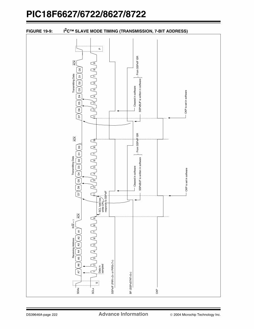
PIC18F6627/6722/8627/8722
DS39646A-page 222 Advance Information 2004 Microchip Technology Inc.
FIGURE 19-9: I2C™ SLAVE MODE TIMING (TRANSMISSION, 7-BIT ADDRESS)
SD
Ax
SC
Lx
BF
(S
SP
xSTA
T<
0>)
A6
A5
A4
A3
A2
A1
D6
D5
D4
D3
D2
D1
D0
12
34
56
78
23
45
67
89
SS
PxB
UF
is w
ritte
n in
sof
twar
e
Cle
ared
in s
oftw
are
Fro
m S
SP
xIF
ISR
Dat
a in
sa
mpl
ed
S
AC
KTr
ansm
ittin
g D
ata
R/W
= 0
AC
K
Rec
eivi
ng A
ddre
ss
A7
D7
91
D6
D5
D4
D3
D2
D1
D0
23
45
67
89
SS
PxB
UF
is w
ritte
n in
sof
twar
e
Cle
ared
in s
oftw
are
Fro
m S
SP
xIF
ISR
Tran
smitt
ing
Dat
a
D7 1
CK
P
P
AC
K
CK
P is
set
in s
oftw
are
CK
P is
set
in s
oftw
are
SC
L he
ld lo
ww
hile
CP
Ure
spon
ds to
SS
PxI
F
SS
PxI
F (
PIR
1<3>
or
PIR
3<7>
)

2004 Microchip Technology Inc. Advance Information DS39646A-page 223
PIC18F6627/6722/8627/8722
FIGURE 19-10: I2C™ SLAVE MODE TIMING WITH SEN = 0 (RECEPTION, 10-BIT ADDRESS)
SD
Ax
SC
Lx
SS
PxI
F
BF
(S
SP
xSTA
T<
0>)
S1
23
45
67
89
12
34
56
78
91
23
45
78
9P
11
11
0A
9A
8A
7A
6A
5A
4A
3A
2A
1A
0D
7D
6D
5D
4D
3D
1D
0
Rec
eive
Dat
a B
yte
AC
K
R/W
= 0 AC
K
Rec
eive
Firs
t Byt
e of
Add
ress
Cle
ared
in s
oftw
are
D2
6
(PIR
1<3>
Cle
ared
in s
oftw
are
Rec
eive
Sec
ond
Byt
e of
Add
ress
Cle
ared
by
hard
war
ew
hen
SS
PxA
DD
is u
pdat
edw
ith lo
w b
yte
of a
ddre
ss
UA
(S
SP
xSTA
T<
1>)
Clo
ck is
hel
d lo
w u
ntil
upda
te o
f SS
PxA
DD
has
ta
ken
plac
e
UA
is s
et in
dica
ting
that
the
SS
PxA
DD
nee
ds to
be
upda
ted
UA
is s
et in
dica
ting
that
SS
PxA
DD
nee
ds to
be
upda
ted
Cle
ared
by
hard
war
e w
hen
SS
PxA
DD
is u
pdat
ed w
ith h
igh
byte
of a
ddre
ss
SS
PxB
UF
is w
ritte
n w
ithco
nten
ts o
f SS
PxS
RD
umm
y re
ad o
f SS
PxB
UF
to c
lear
BF
flag
AC
K
CK
P
12
34
57
89
D7
D6
D5
D4
D3
D1
D0
Rec
eive
Dat
a B
yte
Bus
mas
ter
term
inat
estr
ansf
er
D2 6
AC
K
Cle
ared
in s
oftw
are
Cle
ared
in s
oftw
are
SS
PO
V (
SS
PxC
ON
1<6>
)
SS
PO
V is
set
beca
use
SS
PxB
UF
isst
ill fu
ll. A
CK
is n
ot s
ent.
(CK
P d
oes
not r
eset
to ‘0
’ whe
n S
EN
= 0
)
Clo
ck is
hel
d lo
w u
ntil
upda
te o
f SS
PxA
DD
has
ta
ken
plac
e
or P
IR3<
7>)
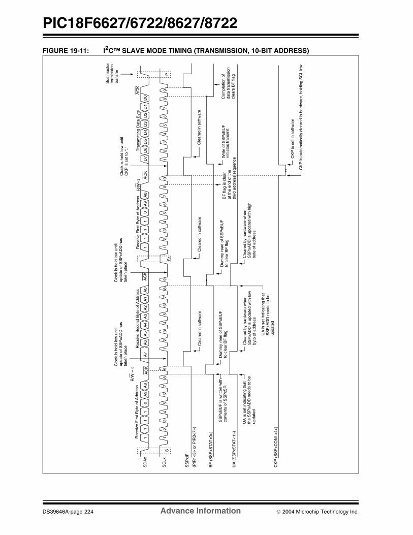
PIC18F6627/6722/8627/8722
DS39646A-page 224 Advance Information 2004 Microchip Technology Inc.
FIGURE 19-11: I2C™ SLAVE MODE TIMING (TRANSMISSION, 10-BIT ADDRESS)
SD
Ax
SC
Lx
SS
PxI
F
BF
(S
SP
xSTA
T<
0>)
S1
23
45
67
89
12
34
56
78
91
23
45
78
9P
11
11
0A
9A
8A
7A
6A
5A
4A
3A
2A
1A
01
11
10
A8
R/W
=1 A
CK
AC
K
R/W
= 0
AC
K
Rec
eive
Firs
t Byt
e of
Add
ress
Cle
ared
in s
oftw
are
Bus
mas
ter
term
inat
estr
ansf
er
A9 6
(PIR
1<3>
or
PIR
3<7>
)
Rec
eive
Sec
ond
Byt
e of
Add
ress
Cle
ared
by
hard
war
e w
hen
SS
PxA
DD
is u
pdat
ed w
ith lo
wby
te o
f add
ress
UA
(S
SP
xSTA
T<
1>)
Clo
ck is
hel
d lo
w u
ntil
upda
te o
f SS
PxA
DD
has
ta
ken
plac
e
UA
is s
et in
dica
ting
that
the
SS
PxA
DD
nee
ds to
be
upda
ted
UA
is s
et in
dica
ting
that
SS
PxA
DD
nee
ds to
be
upda
ted
Cle
ared
by
hard
war
e w
hen
SS
PxA
DD
is u
pdat
ed w
ith h
igh
byte
of a
ddre
ss.
SS
PxB
UF
is w
ritte
n w
ithco
nten
ts o
f SS
PxS
RD
umm
y re
ad o
f SS
PxB
UF
to c
lear
BF
flag
Rec
eive
Firs
t Byt
e of
Add
ress
12
34
57
89
D7
D6
D5
D4
D3
D1
AC
K
D2
6
Tra
nsm
ittin
g D
ata
Byt
e
D0
Dum
my
read
of S
SP
xBU
Fto
cle
ar B
F fl
ag
Sr
Cle
ared
in s
oftw
are
Writ
e of
SS
PxB
UF
initi
ates
tran
smit
Cle
ared
in s
oftw
are
Com
plet
ion
of
clea
rs B
F fl
ag
CK
P (
SS
PxC
ON
1<4>
)
CK
P is
set
in s
oftw
are
CK
P is
aut
omat
ical
ly c
lear
ed in
har
dwar
e, h
oldi
ng S
CL
low
Clo
ck is
hel
d lo
w u
ntil
upda
te o
f SS
PxA
DD
has
ta
ken
plac
e
data
tran
smis
sion
Clo
ck is
hel
d lo
w u
ntil
CK
P is
set
to ‘1
’
third
add
ress
seq
uenc
e
BF
flag
is c
lear
at th
e en
d of
the
2004 Microchip Technology Inc. Advance Information DS39646A-page 225
PIC18F6627/6722/8627/8722
19.4.4 CLOCK STRETCHING
Both 7-bit and 10-bit Slave modes implementautomatic clock stretching during a transmit sequence.
The SEN bit (SSPxCON2<0>) allows clock stretchingto be enabled during receives. Setting SEN will causethe SCL pin to be held low at the end of each datareceive sequence.
19.4.4.1 Clock Stretching for 7-bit Slave Receive Mode (SEN = 1)
In 7-bit Slave Receive mode, on the falling edge of theninth clock at the end of the ACK sequence if the BFbit is set, the CKP bit in the SSPxCON1 register isautomatically cleared, forcing the SCL output to beheld low. The CKP being cleared to ‘0’ will assert theSCL line low. The CKP bit must be set in the user’sISR before reception is allowed to continue. By holdingthe SCL line low, the user has time to service the ISRand read the contents of the SSPxBUF before themaster device can initiate another receive sequence.This will prevent buffer overruns from occurring (seeFigure 19-13).
19.4.4.2 Clock Stretching for 10-bit Slave Receive Mode (SEN = 1)
In 10-bit Slave Receive mode during the addresssequence, clock stretching automatically takes placebut CKP is not cleared. During this time, if the UA bit isset after the ninth clock, clock stretching is initiated.The UA bit is set after receiving the upper byte of the10-bit address and following the receive of the secondbyte of the 10-bit address with the R/W bit cleared to‘0’. The release of the clock line occurs upon updatingSSPxADD. Clock stretching will occur on each datareceive sequence as described in 7-bit mode.
19.4.4.3 Clock Stretching for 7-bit Slave Transmit Mode
The 7-bit Slave Transmit mode implements clockstretching by clearing the CKP bit after the falling edgeof the ninth clock if the BF bit is clear. This occursregardless of the state of the SEN bit.
The user’s ISR must set the CKP bit before transmis-sion is allowed to continue. By holding the SCLx linelow, the user has time to service the ISR and load thecontents of the SSPxBUF before the master devicecan initiate another transmit sequence (seeFigure 19-9).
19.4.4.4 Clock Stretching for 10-bit Slave Transmit Mode
In 10-bit Slave Transmit mode, clock stretching is con-trolled during the first two address sequences by thestate of the UA bit, just as it is in 10-bit Slave Receivemode. The first two addresses are followed by a thirdaddress sequence which contains the high-order bitsof the 10-bit address and the R/W bit set to ‘1’. Afterthe third address sequence is performed, the UA bit isnot set, the module is now configured in Transmitmode and clock stretching is controlled by the BF flagas in 7-bit Slave Transmit mode (see Figure 19-11).
Note 1: If the user reads the contents of theSSPxBUF before the falling edge of theninth clock, thus clearing the BF bit, theCKP bit will not be cleared and clockstretching will not occur.
2: The CKP bit can be set in softwareregardless of the state of the BF bit. Theuser should be careful to clear the BF bitin the ISR before the next receivesequence in order to prevent an overflowcondition.
Note: If the user polls the UA bit and clears it byupdating the SSPxADD register before thefalling edge of the ninth clock occurs and ifthe user hasn’t cleared the BF bit by read-ing the SSPxBUF register before that time,then the CKP bit will still NOT be assertedlow. Clock stretching on the basis of thestate of the BF bit only occurs during adata sequence, not an address sequence.
Note 1: If the user loads the contents ofSSPxBUF, setting the BF bit before thefalling edge of the ninth clock, the CKP bitwill not be cleared and clock stretchingwill not occur.
2: The CKP bit can be set in softwareregardless of the state of the BF bit.

PIC18F6627/6722/8627/8722
DS39646A-page 226 Advance Information 2004 Microchip Technology Inc.
19.4.4.5 Clock Synchronization and the CKP bit
When the CKP bit is cleared, the SCLx output is forcedto ‘0’. However, clearing the CKP bit will not assert theSCLx output low until the SCLx output is already sam-pled low. Therefore, the CKP bit will not assert theSCLx line until an external I2C master device has
already asserted the SCLx line. The SCLx output willremain low until the CKP bit is set and all otherdevices on the I2C bus have deasserted SCLx. Thisensures that a write to the CKP bit will not violate theminimum high time requirement for SCLx (seeFigure 19-12).
FIGURE 19-12: CLOCK SYNCHRONIZATION TIMING
SDAx
SCLx
DX-1DX
WR
Q1 Q2 Q3 Q4 Q1 Q2 Q3 Q4 Q1 Q2 Q3 Q4 Q1 Q2 Q3 Q4 Q1 Q2 Q3 Q4 Q1 Q2 Q3 Q4 Q1 Q2 Q3 Q4
SSPxCON
CKP
Master devicedeasserts clock
Master deviceasserts clock

2004 Microchip Technology Inc. Advance Information DS39646A-page 227
PIC18F6627/6722/8627/8722
FIGURE 19-13: I2C™ SLAVE MODE TIMING WITH SEN = 1 (RECEPTION, 7-BIT ADDRESS)
SD
Ax
SC
Lx
SS
PxI
F
BF
(S
SP
xSTA
T<
0>)
SS
PO
V (
SS
PxC
ON
1<6>
)
S1
23
45
67
89
12
34
56
78
91
23
45
78
9P
A7
A6
A5
A4
A3
A2
A1
D7
D6
D5
D4
D3
D2
D1
D0
D7
D6
D5
D4
D3
D1
D0
AC
KR
ecei
ving
Dat
aA
CK
Rec
eivi
ng D
ata
R/W
= 0 AC
K
Rec
eivi
ng A
ddre
ss
Cle
ared
in s
oftw
are
SS
PxB
UF
is r
ead
Bus
mas
ter
term
inat
estr
ansf
er
SS
PO
V is
set
beca
use
SS
PxB
UF
isst
ill fu
ll. A
CK
is n
ot s
ent.
D2 6
(PIR
1<3>
or
PIR
3<7>
)
CK
P
CK
Pw
ritte
nto
‘1’ i
nIf
BF
is c
lear
edpr
ior
to th
e fa
lling
edge
of t
he 9
th c
lock
,C
KP
will
not
be
rese
tto
‘0’ a
nd n
o cl
ock
stre
tchi
ng w
ill o
ccur
softw
are
Clo
ck is
hel
d lo
w u
ntil
CK
P is
set
to ‘1
’
Clo
ck is
not
hel
d lo
wbe
caus
e bu
ffer
full
bit i
s cl
ear
prio
r to
falli
ng e
dge
of 9
th c
lock
C
lock
is n
ot h
eld
low
beca
use
AC
K =
1
BF
is s
et a
fter
falli
ng
edge
of t
he 9
th c
lock
,C
KP
is r
eset
to ‘0
’ and
cloc
k st
retc
hing
occ
urs

PIC18F6627/6722/8627/8722
DS39646A-page 228 Advance Information 2004 Microchip Technology Inc.
FIGURE 19-14: I2C™ SLAVE MODE TIMING WITH SEN = 1 (RECEPTION, 10-BIT ADDRESS)
SD
Ax
SC
Lx
SS
PxI
F
BF
(S
SP
xSTA
T<
0>)
S1
23
45
67
89
12
34
56
78
91
23
45
78
9P
11
11
0A
9A
8A
7A
6A
5A
4A
3A
2A
1A
0D
7D
6D
5D
4D
3D
1D
0
Rec
eive
Dat
a B
yte
AC
K
R/W
= 0
AC
K
Rec
eive
Firs
t Byt
e of
Add
ress
Cle
ared
in s
oftw
are
D2 6
(PIR
1<3>
Cle
ared
in s
oftw
are
Rec
eive
Sec
ond
Byt
e of
Add
ress
Cle
ared
by
hard
war
e w
hen
SS
PxA
DD
is u
pdat
ed w
ith lo
wby
te o
f add
ress
afte
r fa
lling
edg
e
UA
(S
SP
xSTA
T<
1>)
Clo
ck is
hel
d lo
w u
ntil
upda
te o
f SS
PxA
DD
has
ta
ken
plac
e
UA
is s
et in
dica
ting
that
the
SS
PxA
DD
nee
ds to
be
upda
ted
UA
is s
et in
dica
ting
that
SS
PxA
DD
nee
ds to
be
upda
ted
Cle
ared
by
hard
war
e w
hen
SS
PxA
DD
is u
pdat
ed w
ith h
igh
byte
of a
ddre
ss a
fter
falli
ng e
dge
SS
PxB
UF
is w
ritte
n w
ithco
nten
ts o
f SS
PxS
RD
umm
y re
ad o
f SS
PxB
UF
to c
lear
BF
flag
AC
K
CK
P
12
34
57
89
D7
D6
D5
D4
D3
D1
D0
Rec
eive
Dat
a B
yte
Bus
mas
ter
term
inat
estr
ansf
er
D2 6
AC
K
Cle
ared
in s
oftw
are
Cle
ared
in s
oftw
are
SS
PO
V (
SS
PxC
ON
1<6>
)
CK
P w
ritte
n to
‘1’
No
te:
An
upda
te
of
the
SS
PxA
DD
re
gist
erbe
fore
the
fal
ling
edge
of
the
nint
h cl
ock
will
hav
e no
effe
ct o
n U
A a
nd U
A w
ill
No
te:
An
upda
te o
f th
e S
SP
xAD
Dre
gist
er
befo
re
the
falli
nged
ge o
f th
e ni
nth
cloc
k w
illha
ve n
o ef
fect
on
UA
and
UA
will
rem
ain
set.
in s
oftw
are
Clo
ck is
hel
d lo
w u
ntil
upda
te o
f SS
PxA
DD
has
ta
ken
plac
e of n
inth
clo
ckof
nin
th c
lock
SS
PO
V is
set
beca
use
SS
PxB
UF
isst
ill fu
ll. A
CK
is n
ot s
ent.
Dum
my
read
of S
SP
xBU
Fto
cle
ar B
F fl
ag
Clo
ck is
hel
d lo
w u
ntil
CK
P is
set
to ‘1
’C
lock
is n
ot h
eld
low
beca
use
AC
K =
1
or P
IR3<
7>)

2004 Microchip Technology Inc. Advance Information DS39646A-page 229
PIC18F6627/6722/8627/8722
19.4.5 GENERAL CALL ADDRESS SUPPORT
The addressing procedure for the I2C bus is such thatthe first byte after the Start condition usuallydetermines which device will be the slave addressed bythe master. The exception is the general call addresswhich can address all devices. When this address isused, all devices should, in theory, respond with anAcknowledge.
The general call address is one of eight addressesreserved for specific purposes by the I2C protocol. Itconsists of all ‘0’s with R/W = 0.
The general call address is recognized when theGeneral Call Enable bit, GCEN, is enabled(SSPxCON2<7> set). Following a Start bit detect, 8 bitsare shifted into the SSPxSR and the address is com-pared against the SSPxADD. It is also compared to thegeneral call address and fixed in hardware.
If the general call address matches, the SSPxSR istransferred to the SSPxBUF, the BF flag bit is set(eighth bit) and on the falling edge of the ninth bit (ACKbit), the SSPxIF interrupt flag bit is set.
When the interrupt is serviced, the source for theinterrupt can be checked by reading the contents of theSSPxBUF. The value can be used to determine if theaddress was device specific or a general call address.
In 10-bit mode, the SSPxADD is required to be updatedfor the second half of the address to match and the UAbit is set (SSPxSTAT<1>). If the general call address issampled when the GCEN bit is set, while the slave isconfigured in 10-bit Address mode, then the secondhalf of the address is not necessary, the UA bit will notbe set and the slave will begin receiving data after theAcknowledge (Figure 19-15).
FIGURE 19-15: SLAVE MODE GENERAL CALL ADDRESS SEQUENCE (7 OR 10-BIT ADDRESS MODE)
SDAx
SCLx
S
SSPxIF
BF (SSPxSTAT<0>)
SSPOV (SSPxCON1<6>)
Cleared in software
SSPxBUF is read
R/W = 0
ACKGeneral Call Address
Address is compared to General Call Address
GCEN (SSPxCON2<7>)
Receiving Data ACK
1 2 3 4 5 6 7 8 9 1 2 3 4 5 6 7 8 9
D7 D6 D5 D4 D3 D2 D1 D0
after ACK, set interrupt
‘0’
‘1’

PIC18F6627/6722/8627/8722
DS39646A-page 230 Advance Information 2004 Microchip Technology Inc.
19.4.6 MASTER MODE
Master mode is enabled by setting and clearing theappropriate SSPM bits in SSPxCON1 and by settingthe SSPEN bit. In Master mode, the SCLx and SDAxlines are manipulated by the MSSP hardware if theTRIS bits are set.
Master mode of operation is supported by interruptgeneration on the detection of the Start and Stop con-ditions. The Stop (P) and Start (S) bits are cleared froma Reset or when the MSSP module is disabled. Controlof the I2C bus may be taken when the P bit is set, or thebus is Idle, with both the S and P bits clear.
In Firmware Controlled Master mode, user codeconducts all I2C bus operations based on Start andStop bit conditions.
Once Master mode is enabled, the user has sixoptions.
1. Assert a Start condition on SDAx and SCLx.
2. Assert a Repeated Start condition on SDAx andSCLx.
3. Write to the SSPxBUF register initiatingtransmission of data/address.
4. Configure the I2C port to receive data.5. Generate an Acknowledge condition at the end
of a received byte of data.6. Generate a Stop condition on SDAx and SCxL.
The following events will cause the SSP Interrupt Flagbit, SSPxIF, to be set (and SSP interrupt, if enabled):
• Start condition
• Stop condition• Data transfer byte transmitted/received• Acknowledge transmit
• Repeated Start
FIGURE 19-16: MSSP BLOCK DIAGRAM (I2C™ MASTER MODE)
Note: The MSSP module, when configured inI2C Master mode, does not allow queueingof events. For instance, the user is notallowed to initiate a Start condition andimmediately write the SSPxBUF register toinitiate transmission before the Start condi-tion is complete. In this case, theSSPxBUF will not be written to and theWCOL bit will be set, indicating that a writeto the SSPxBUF did not occur.
Read Write
SSPxSR
Start bit, Stop bit,
SSPxBUF
InternalData Bus
Set/Reset, S, P, WCOL (SSPxSTAT)
ShiftClock
MSb LSb
SDAx
AcknowledgeGenerate
Stop bit DetectWrite Collision Detect
Clock ArbitrationState Counter forend of XMIT/RCV
SCLx
SCL In
Bus Collision
SDA In
Rec
eive
Ena
ble
Clo
ck C
ntl
Clo
ck A
rbitr
ate/
WC
OL
Det
ect
(hol
d of
f clo
ck s
ourc
e)SSPxADD<6:0>
Baud
Set SSPxIF, BCLxIFReset ACKSTAT, PEN (SSPxCON2)
RateGenerator
SSPM3:SSPM0
Start bit Detect
2004 Microchip Technology Inc. Advance Information DS39646A-page 231
PIC18F6627/6722/8627/8722
19.4.6.1 I2C Master Mode Operation
The master device generates all of the serial clockpulses and the Start and Stop conditions. A transfer isended with a Stop condition or with a Repeated Startcondition. Since the Repeated Start condition is alsothe beginning of the next serial transfer, the I2C bus willnot be released.
In Master Transmitter mode, serial data is outputthrough SDAx, while SCLx outputs the serial clock. Thefirst byte transmitted contains the slave address of thereceiving device (7 bits) and the Read/Write (R/W) bit.In this case, the R/W bit will be logic ‘0’. Serial data istransmitted 8 bits at a time. After each byte is transmit-ted, an Acknowledge bit is received. Start and Stopconditions are output to indicate the beginning and theend of a serial transfer.
In Master Receive mode, the first byte transmitted con-tains the slave address of the transmitting device(7 bits) and the R/W bit. In this case, the R/W bit will belogic ‘1’. Thus, the first byte transmitted is a 7-bit slaveaddress followed by a ‘1’ to indicate the receive bit.Serial data is received via SDA, while SCL outputs theserial clock. Serial data is received 8 bits at a time. Aftereach byte is received, an Acknowledge bit is transmit-ted. Start and Stop conditions indicate the beginningand end of transmission.
The Baud Rate Generator used for the SPI modeoperation is used to set the SCLx clock frequency foreither 100 kHz, 400 kHz or 1 MHz I2C operation. SeeSection 19.4.7 “Baud Rate” for more detail.
A typical transmit sequence would go as follows:
1. The user generates a Start condition by settingthe Start Enable bit, SEN (SSPxCON2<0>).
2. SSPxIF is set. The MSSP module will wait therequired start time before any other operationtakes place.
3. The user loads the SSPxBUF with the slaveaddress to transmit.
4. Address is shifted out the SDAx pin until all 8 bitsare transmitted.
5. The MSSP module shifts in the ACK bit from theslave device and writes its value into theSSPxCON2 register (SSPxCON2<6>).
6. The MSSP module generates an interrupt at theend of the ninth clock cycle by setting theSSPxIF bit.
7. The user loads the SSPxBUF with eight bits ofdata.
8. Data is shifted out the SDAx pin until all 8 bitsare transmitted.
9. The MSSP module shifts in the ACK bit from theslave device and writes its value into theSSPxCON2 register (SSPxCON2<6>).
10. The MSSP module generates an interrupt at theend of the ninth clock cycle by setting theSSPxIF bit.
11. The user generates a Stop condition by settingthe Stop Enable bit, PEN (SSPxCON2<2>).
12. Interrupt is generated once the Stop condition iscomplete.

PIC18F6627/6722/8627/8722
DS39646A-page 232 Advance Information 2004 Microchip Technology Inc.
19.4.7 BAUD RATE
In I2C Master mode, the Baud Rate Generator (BRG)reload value is placed in the lower 7 bits of theSSPxADD register (Figure 19-17). When a writeoccurs to SSPxBUF, the Baud Rate Generator willautomatically begin counting. The BRG counts down to‘0’ and stops until another reload has taken place. TheBRG count is decremented twice per instruction cycle(TCY) on the Q2 and Q4 clocks. In I2C Master mode, theBRG is reloaded automatically.
Once the given operation is complete (i.e., transmis-sion of the last data bit is followed by ACK), the internalclock will automatically stop counting and the SCLx pinwill remain in its last state.
Table 19-3 demonstrates clock rates based oninstruction cycles and the BRG value loaded intoSSPxADD.
19.4.7.1 Baud Rate and Module Interdependence
Because MSSP1 and MSSP2 are independent, theycan operate simultaneously in I2C Master mode at dif-ferent baud rates. This is done by using different BRGreload values for each module.
Because this mode derives its basic clock source fromthe system clock, any changes to the clock will affectboth modules in the same proportion. It may be possi-ble to change one or both baud rates back to a previousvalue by changing the BRG reload value.
FIGURE 19-17: BAUD RATE GENERATOR BLOCK DIAGRAM
TABLE 19-3: I2C™ CLOCK RATE W/BRG
SSPM3:SSPM0
BRG Down CounterCLKO FOSC/4
SSPxADD<6:0>
SSPM3:SSPM0
SCLx
Reload
Control
Reload
FOSC FCY FCY*2 BRG ValueFSCL
(2 Rollovers of BRG)
40 MHz 10 MHz 20 MHz 18h 400 kHz(1)
40 MHz 10 MHz 20 MHz 1Fh 312.5 kHz
40 MHz 10 MHz 20 MHz 63h 100 kHz
16 MHz 4 MHz 8 MHz 09h 400 kHz(1)
16 MHz 4 MHz 8 MHz 0Ch 308 kHz
16 MHz 4 MHz 8 MHz 27h 100 kHz
4 MHz 1 MHz 2 MHz 02h 333 kHz(1)
4 MHz 1 MHz 2 MHz 09h 100 kHz
4 MHz 1 MHz 2 MHz 00h 1 MHz(1)
Note 1: The I2C interface does not conform to the 400 kHz I2C specification (which applies to rates greater than 100 kHz) in all details, but may be used with care where higher rates are required by the application.

2004 Microchip Technology Inc. Advance Information DS39646A-page 233
PIC18F6627/6722/8627/8722
19.4.7.2 Clock Arbitration
Clock arbitration occurs when the master, during anyreceive, transmit or Repeated Start/Stop condition,deasserts the SCL pin (SCL allowed to float high).When the SCL pin is allowed to float high, the BaudRate Generator (BRG) is suspended from countinguntil the SCL pin is actually sampled high. When the
SCL pin is sampled high, the Baud Rate Generator isreloaded with the contents of SSPxADD<6:0> andbegins counting. This ensures that the SCL high timewill always be at least one BRG rollover count in theevent that the clock is held low by an external device(Figure 19-18).
FIGURE 19-18: BAUD RATE GENERATOR TIMING WITH CLOCK ARBITRATION
SDAx
SCLx
SCLx deasserted but slave holds
DX-1DX
BRG
SCLx is sampled high, reload takesplace and BRG starts its count
03h 02h 01h 00h (hold off) 03h 02h
Reload
BRGValue
SCLx low (clock arbitration)SCL allowed to transition high
BRG decrements onQ2 and Q4 cycles
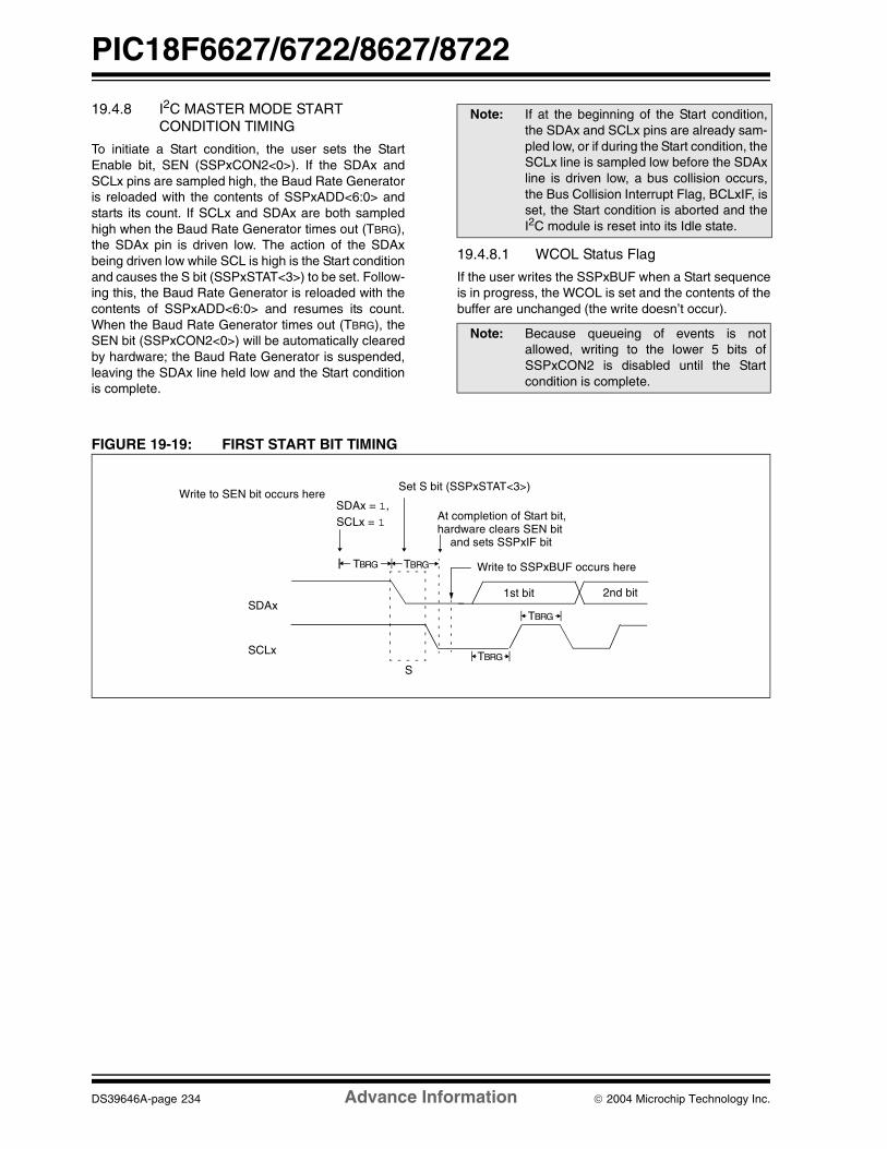
PIC18F6627/6722/8627/8722
DS39646A-page 234 Advance Information 2004 Microchip Technology Inc.
19.4.8 I2C MASTER MODE START CONDITION TIMING
To initiate a Start condition, the user sets the StartEnable bit, SEN (SSPxCON2<0>). If the SDAx andSCLx pins are sampled high, the Baud Rate Generatoris reloaded with the contents of SSPxADD<6:0> andstarts its count. If SCLx and SDAx are both sampledhigh when the Baud Rate Generator times out (TBRG),the SDAx pin is driven low. The action of the SDAxbeing driven low while SCL is high is the Start conditionand causes the S bit (SSPxSTAT<3>) to be set. Follow-ing this, the Baud Rate Generator is reloaded with thecontents of SSPxADD<6:0> and resumes its count.When the Baud Rate Generator times out (TBRG), theSEN bit (SSPxCON2<0>) will be automatically clearedby hardware; the Baud Rate Generator is suspended,leaving the SDAx line held low and the Start conditionis complete.
19.4.8.1 WCOL Status Flag
If the user writes the SSPxBUF when a Start sequenceis in progress, the WCOL is set and the contents of thebuffer are unchanged (the write doesn’t occur).
FIGURE 19-19: FIRST START BIT TIMING
Note: If at the beginning of the Start condition,the SDAx and SCLx pins are already sam-pled low, or if during the Start condition, theSCLx line is sampled low before the SDAxline is driven low, a bus collision occurs,the Bus Collision Interrupt Flag, BCLxIF, isset, the Start condition is aborted and theI2C module is reset into its Idle state.
Note: Because queueing of events is notallowed, writing to the lower 5 bits ofSSPxCON2 is disabled until the Startcondition is complete.
SDAx
SCLx
S
TBRG
1st bit 2nd bit
TBRG
SDAx = 1, At completion of Start bit,SCLx = 1
Write to SSPxBUF occurs hereTBRG
hardware clears SEN bit
TBRG
Write to SEN bit occurs hereSet S bit (SSPxSTAT<3>)
and sets SSPxIF bit

2004 Microchip Technology Inc. Advance Information DS39646A-page 235
PIC18F6627/6722/8627/8722
19.4.9 I2C MASTER MODE REPEATED START CONDITION TIMING
A Repeated Start condition occurs when the RSEN bit(SSPxCON2<1>) is programmed high and the I2C logicmodule is in the Idle state. When the RSEN bit is set,the SCL pin is asserted low. When the SCLx pin is sam-pled low, the Baud Rate Generator is loaded with thecontents of SSPxADD<5:0> and begins counting. TheSDAx pin is released (brought high) for one Baud RateGenerator count (TBRG). When the Baud Rate Genera-tor times out, if SDAx is sampled high, the SCLx pin willbe deasserted (brought high). When SCLx is sampledhigh, the Baud Rate Generator is reloaded with thecontents of SSPxADD<6:0> and begins counting.SDAx and SCLx must be sampled high for one TBRG.This action is then followed by assertion of the SDAxpin (SDAx = 0) for one TBRG while SCL is high. Follow-ing this, the RSEN bit (SSPxCON2<1>) will be auto-matically cleared and the Baud Rate Generator will notbe reloaded, leaving the SDAx pin held low. As soon asa Start condition is detected on the SDAx and SCLxpins, the S bit (SSPxSTAT<3>) will be set. The SSPxIFbit will not be set until the Baud Rate Generator hastimed out.
Immediately following the SSPxIF bit getting set, theuser may write the SSPxBUF with the 7-bit address in7-bit mode or the default first address in 10-bit mode.After the first eight bits are transmitted and an ACK isreceived, the user may then transmit an additional eightbits of address (10-bit mode) or eight bits of data (7-bitmode).
19.4.9.1 WCOL Status Flag
If the user writes the SSPxBUF when a Repeated Startsequence is in progress, the WCOL is set and thecontents of the buffer are unchanged (the write doesn’toccur).
FIGURE 19-20: REPEAT START CONDITION WAVEFORM
Note 1: If RSEN is programmed while any otherevent is in progress, it will not take effect.
2: A bus collision during the Repeated Startcondition occurs if:
• SDA is sampled low when SCL goes from low-to-high.
• SCL goes low before SDA is asserted low. This may indicate that another master is attempting to transmit a data ‘1’.
Note: Because queueing of events is notallowed, writing of the lower 5 bits ofSSPxCON2 is disabled until the RepeatedStart condition is complete.
SDAx
SCLx
Sr = Repeated Start
Write to SSPxCON2
Write to SSPxBUF occurs hereon falling edge of ninth clock,
end of Xmit
At completion of Start bit, hardware clears RSEN bit
1st bit
S bit set by hardware
TBRG
TBRG
SDAx = 1,
SDAx = 1,
SCLx (no change).SCLx = 1occurs here:
TBRG TBRG TBRG
and sets SSPxIF
RSEN bit set by hardware

PIC18F6627/6722/8627/8722
DS39646A-page 236 Advance Information 2004 Microchip Technology Inc.
19.4.10 I2C MASTER MODE TRANSMISSION
Transmission of a data byte, a 7-bit address or theother half of a 10-bit address is accomplished by simplywriting a value to the SSPxBUF register. This action willset the Buffer Full flag bit, BF and allow the Baud RateGenerator to begin counting and start the next trans-mission. Each bit of address/data will be shifted outonto the SDAx pin after the falling edge of SCLx isasserted (see data hold time specificationparameter 106). SCLx is held low for one Baud RateGenerator rollover count (TBRG). Data should be validbefore SCL is released high (see data setup time spec-ification parameter 107). When the SCLx pin isreleased high, it is held that way for TBRG. The data onthe SDAx pin must remain stable for that duration andsome hold time after the next falling edge of SCLx.After the eighth bit is shifted out (the falling edge of theeighth clock), the BF flag is cleared and the masterreleases SDAx. This allows the slave device beingaddressed to respond with an ACK bit during the ninthbit time if an address match occurred, or if data wasreceived properly. The status of ACK is written into theACKDT bit on the falling edge of the ninth clock. If themaster receives an Acknowledge, the AcknowledgeStatus bit, ACKSTAT, is cleared. If not, the bit is set.After the ninth clock, the SSPxIF bit is set and themaster clock (Baud Rate Generator) is suspended untilthe next data byte is loaded into the SSPxBUF, leavingSCLx low and SDAx unchanged (Figure 19-21).
After the write to the SSPxBUF, each bit of the addresswill be shifted out on the falling edge of SCLx until allseven address bits and the R/W bit are completed. Onthe falling edge of the eighth clock, the master willdeassert the SDAx pin, allowing the slave to respondwith an Acknowledge. On the falling edge of the ninthclock, the master will sample the SDAx pin to see if theaddress was recognized by a slave. The status of theACK bit is loaded into the ACKSTAT status bit(SSPxCON2<6>). Following the falling edge of theninth clock transmission of the address, the SSPxIF isset, the BF flag is cleared and the Baud Rate Generatoris turned off until another write to the SSPxBUF takesplace, holding SCL low and allowing SDA to float.
19.4.10.1 BF Status Flag
In Transmit mode, the BF bit (SSPxSTAT<0>) is setwhen the CPU writes to SSPxBUF and is cleared whenall 8 bits are shifted out.
19.4.10.2 WCOL Status Flag
If the user writes the SSPxBUF when a transmit isalready in progress (i.e., SSPxSR is still shifting out adata byte), the WCOL is set and the contents of thebuffer are unchanged (the write doesn’t occur) after 2TCY after the SSPxBUF write. If SSPxBUF is rewrittenwithin 2 TCY, the WCOL bit is set and SSPxBUF isupdated. This may result in a corrupted transfer.
The user should verify that the WCOL is clear aftereach write to SSPxBUF to ensure the transfer iscorrect. In all cases, WCOL must be cleared in soft-ware.
19.4.10.3 ACKSTAT Status Flag
In Transmit mode, the ACKSTAT bit (SSPxCON2<6>)is cleared when the slave has sent an Acknowledge(ACK = 0) and is set when the slave does not Acknowl-edge (ACK = 1). A slave sends an Acknowledge whenit has recognized its address (including a general call),or when the slave has properly received its data.
19.4.11 I2C MASTER MODE RECEPTION
Master mode reception is enabled by programming theReceive Enable bit, RCEN (SSPxCON2<3>).
The Baud Rate Generator begins counting and on eachrollover, the state of the SCLx pin changes(high-to-low/low-to-high) and data is shifted into theSSPxSR. After the falling edge of the eighth clock, thereceive enable flag is automatically cleared, the con-tents of the SSPxSR are loaded into the SSPxBUF, theBF flag bit is set, the SSPxIF flag bit is set and the BaudRate Generator is suspended from counting, holdingSCL low. The MSSP is now in Idle state awaiting thenext command. When the buffer is read by the CPU,the BF flag bit is automatically cleared. The user canthen send an Acknowledge bit at the end of receptionby setting the Acknowledge Sequence Enable bit,ACKEN (SSPxCON2<4>).
19.4.11.1 BF Status Flag
In receive operation, the BF bit is set when an addressor data byte is loaded into SSPxBUF from SSPxSR. Itis cleared when the SSPxBUF register is read.
19.4.11.2 SSPOV Status Flag
In receive operation, the SSPOV bit is set when 8 bitsare received into the SSPxSR and the BF flag bit isalready set from a previous reception.
Note: The MSSP module must be in an Idle statebefore the RCEN bit is set or the RCEN bitwill be disregarded.

2004 Microchip Technology Inc. Advance Information DS39646A-page 237
PIC18F6627/6722/8627/8722
19.4.11.3 WCOL Status Flag
If the user writes the SSPxBUF when a receive isalready in progress (i.e., SSPxSR is still shifting in adata byte), the WCOL bit is set and the contents of thebuffer are unchanged (the write doesn’t occur).
FIGURE 19-21: I2C™ MASTER MODE WAVEFORM (TRANSMISSION, 7 OR 10-BIT ADDRESS)
SD
Ax
SC
Lx
SS
PxI
F
BF
(S
SP
xSTA
T<
0>)
SE
N
A7
A6
A5
A4
A3
A2
A1
AC
K =
0D
7D
6D
5D
4D
3D
2D
1D
0
AC
KT
rans
mitt
ing
Dat
a or
Sec
ond
Hal
fR
/W =
0Tr
ansm
it A
ddre
ss to
Sla
ve
12
34
56
78
91
23
45
67
89
P
Cle
ared
in s
oftw
are
serv
ice
rout
ine
SS
PxB
UF
is w
ritte
n in
sof
twar
e
from
SS
P in
terr
upt
Afte
r S
tart
con
ditio
n, S
EN
cle
ared
by
hard
war
e
S
SS
PxB
UF
writ
ten
with
7-b
it ad
dres
s an
d R
/Wst
art t
rans
mit
SC
L he
ld lo
ww
hile
CP
Ure
spon
ds to
SS
PxI
F
SE
N =
0
of 1
0-bi
t Add
ress
Writ
e S
SP
xCO
N2<
0> S
EN
= 1
Sta
rt c
ondi
tion
begi
nsF
rom
sla
ve, c
lear
AC
KS
TAT
bit
SS
PxC
ON
2<6>
AC
KS
TAT
in
SS
PxC
ON
2 =
1
Cle
ared
in s
oftw
are
SS
PxB
UF
writ
ten
PE
N
R/W
Cle
ared
in s
oftw
are

PIC18F6627/6722/8627/8722
DS39646A-page 238 Advance Information 2004 Microchip Technology Inc.
FIGURE 19-22: I2C™ MASTER MODE WAVEFORM (RECEPTION, 7-BIT ADDRESS)
P9
87
65
D0
D1
D2
D3
D4
D5
D6
D7
S
A7
A6
A5
A4
A3
A2
A1
SD
Ax
SC
Lx1
23
45
67
89
12
34
56
78
91
23
4
Bus
mas
ter
term
inat
estr
ansf
er
AC
K
Rec
eivi
ng D
ata
from
Sla
veR
ecei
ving
Dat
a fr
om S
lave
D0
D1
D2
D3
D4
D5
D6
D7
AC
K
R/W
= 0
Tra
nsm
it A
ddre
ss to
Sla
ve
SS
PxI
F
BF
AC
K is
not
sen
t
Writ
e to
SS
PxC
ON
2<0>
(SE
N =
1),
Writ
e to
SS
PxB
UF
occ
urs
here
,A
CK
from
Sla
veMas
ter
conf
igur
ed a
s a
rece
iver
by p
rogr
amm
ing
SS
PxC
ON
2<3>
(R
CE
N =
1)
PE
N b
it =
1w
ritte
n he
re
Dat
a sh
ifted
in o
n fa
lling
edg
e of
CLK
Cle
ared
in s
oftw
are
star
t XM
IT
SE
N =
0
SS
PO
V
SD
A =
0, S
CL
= 1
whi
le C
PU
(SS
PxS
TAT
<0>
)
AC
K
Cle
ared
in s
oftw
are
Cle
ared
in s
oftw
are
Set
SS
PxI
F in
terr
upt
at e
nd o
f rec
eive
Set
P b
it (S
SP
xSTA
T<
4>)
and
SS
PxI
FC
lear
ed in
softw
are
AC
K fr
om M
aste
r
Set
SS
PxI
F a
t end
Set
SS
PxI
F in
terr
upt
at e
nd o
f Ack
now
ledg
ese
quen
ce
Set
SS
PxI
F in
terr
upt
at e
nd o
f Ack
now
-le
dge
sequ
ence
of r
ecei
ve
Set
AC
KE
N, s
tart
Ack
now
ledg
e se
quen
ce
SS
PO
V is
set
bec
ause
SS
PxB
UF
is s
till f
ull
SD
A =
AC
KD
T =
1
RC
EN
cle
ared
auto
mat
ical
lyR
CE
N =
1, s
tart
next
rec
eive
Writ
e to
SS
PxC
ON
2<4>
to s
tart
Ack
now
ledg
e se
quen
ceS
DA
= A
CK
DT
(S
SP
xCO
N2<
5>)
= 0
RC
EN
cle
ared
auto
mat
ical
ly
resp
onds
to S
SP
xIF
AC
KE
Nbegi
n S
tart
con
ditio
n
Cle
ared
in s
oftw
are
SD
A =
AC
KD
T =
0
Last
bit
is s
hifte
d in
to S
SP
xSR
and
cont
ents
are
unl
oade
d in
to S
SP
xBU
F

2004 Microchip Technology Inc. Advance Information DS39646A-page 239
PIC18F6627/6722/8627/8722
19.4.12 ACKNOWLEDGE SEQUENCE TIMING
An Acknowledge sequence is enabled by setting theAcknowledge Sequence Enable bit, ACKEN(SSPxCON2<4>). When this bit is set, the SCLx pin ispulled low and the contents of the Acknowledge data bitare presented on the SDAx pin. If the user wishes togenerate an Acknowledge, then the ACKDT bit shouldbe cleared. If not, the user should set the ACKDT bitbefore starting an Acknowledge sequence. The BaudRate Generator then counts for one rollover period(TBRG) and the SCLx pin is deasserted (pulled high).When the SCL pin is sampled high (clock arbitration),the Baud Rate Generator counts for TBRG. The SCL pinis then pulled low. Following this, the ACKEN bit is auto-matically cleared, the Baud Rate Generator is turned offand the MSSP module then goes into Idle mode(Figure 19-23).
19.4.12.1 WCOL Status Flag
If the user writes the SSPxBUF when an Acknowledgesequence is in progress, then WCOL is set and thecontents of the buffer are unchanged (the write doesn’toccur).
19.4.13 STOP CONDITION TIMING
A Stop bit is asserted on the SDA pin at the end of areceive/transmit by setting the Stop Sequence Enablebit, PEN (SSPxCON2<2>). At the end of areceive/transmit, the SCL line is held low after the fall-ing edge of the ninth clock. When the PEN bit is set, themaster will assert the SDA line low. When the SDA lineis sampled low, the Baud Rate Generator is reloadedand counts down to ‘0’. When the Baud Rate Generatortimes out, the SCL pin will be brought high and oneTBRG (Baud Rate Generator rollover count) later, theSDA pin will be deasserted. When the SDA pin is sam-pled high while SCL is high, the P bit (SSPxSTAT<4>)is set. A TBRG later, the PEN bit is cleared and theSSPxIF bit is set (Figure 19-24).
19.4.13.1 WCOL Status Flag
If the user writes the SSPxBUF when a Stop sequenceis in progress, then the WCOL bit is set and the con-tents of the buffer are unchanged (the write doesn’toccur).
FIGURE 19-23: ACKNOWLEDGE SEQUENCE WAVEFORM
FIGURE 19-24: STOP CONDITION RECEIVE OR TRANSMIT MODE
Note: TBRG = one Baud Rate Generator period.
SDAx
SCLx
SSPxIF set at
Acknowledge sequence starts here,write to SSPxCON2
ACKEN automatically cleared
Cleared in
TBRG TBRG
the end of receive
8
ACKEN = 1, ACKDT = 0
D0
9
SSPxIF
software SSPxIF set at the endof Acknowledge sequence
Cleared insoftware
ACK
SCLx
SDAx
SDA asserted low before rising edge of clock
Write to SSPxCON2,set PEN
Falling edge of
SCLx = 1 for TBRG, followed by SDA = 1 for TBRG
9th clock
SCL brought high after TBRG
Note: TBRG = one Baud Rate Generator period.
TBRG TBRG
after SDAx sampled high. P bit (SSPxSTAT<4>) is set.
TBRG
to setup Stop condition
ACK
PTBRG
PEN bit (SSPxCON2<2>) is cleared by hardware and the SSPxIF bit is set

PIC18F6627/6722/8627/8722
DS39646A-page 240 Advance Information 2004 Microchip Technology Inc.
19.4.14 SLEEP OPERATION
While in Sleep mode, the I2C module can receiveaddresses or data and when an address match or com-plete byte transfer occurs, wake the processor fromSleep (if the MSSP interrupt is enabled).
19.4.15 EFFECTS OF A RESET
A Reset disables the MSSP module and terminates thecurrent transfer.
19.4.16 MULTI-MASTER MODE
In Multi-Master mode, the interrupt generation on thedetection of the Start and Stop conditions allows thedetermination of when the bus is free. The Stop (P) andStart (S) bits are cleared from a Reset or when theMSSP module is disabled. Control of the I2C bus maybe taken when the P bit (SSPxSTAT<4>) is set, or thebus is Idle, with both the S and P bits clear. When thebus is busy, enabling the SSP interrupt will generatethe interrupt when the Stop condition occurs.
In multi-master operation, the SDAx line must bemonitored for arbitration to see if the signal level is theexpected output level. This check is performed inhardware with the result placed in the BCLxIF bit.
The states where arbitration can be lost are:
• Address Transfer
• Data Transfer• A Start Condition • A Repeated Start Condition
• An Acknowledge Condition
19.4.17 MULTI -MASTER COMMUNICATION, BUS COLLISION AND BUS ARBITRATION
Multi-Master mode support is achieved by bus arbitra-tion. When the master outputs address/data bits ontothe SDAx pin, arbitration takes place when the masteroutputs a ‘1’ on SDAx, by letting SDA float high andanother master asserts a ‘0’. When the SCLx pin floatshigh, data should be stable. If the expected data onSDAx is a ‘1’ and the data sampled on the SDAxpin = 0, then a bus collision has taken place. Themaster will set the Bus Collision Interrupt Flag, BCLxIFand reset the I2C port to its Idle state (Figure 19-25).
If a transmit was in progress when the bus collisionoccurred, the transmission is halted, the BF flag iscleared, the SDAx and SCLx lines are deasserted andthe SSPxBUF can be written to. When the userservices the bus collision Interrupt Service Routine andif the I2C bus is free, the user can resume communica-tion by asserting a Start condition.
If a Start, Repeated Start, Stop or Acknowledge condi-tion was in progress when the bus collision occurred, thecondition is aborted, the SDAx and SCLx lines aredeasserted and the respective control bits in theSSPxCON2 register are cleared. When the userservices the bus collision Interrupt Service Routine andif the I2C bus is free, the user can resume communica-tion by asserting a Start condition.
The master will continue to monitor the SDAx and SCLxpins. If a Stop condition occurs, the SSPxIF bit will be set.
A write to the SSPxBUF will start the transmission ofdata at the first data bit, regardless of where thetransmitter left off when the bus collision occurred.
In Multi-Master mode, the interrupt generation on thedetection of Start and Stop conditions allows the deter-mination of when the bus is free. Control of the I2C buscan be taken when the P bit is set in the SSPxSTATregister, or the bus is Idle and the S and P bits arecleared.
FIGURE 19-25: BUS COLLISION TIMING FOR TRANSMIT AND ACKNOWLEDGE
SDAx
SCLx
BCLxIF
SDAx released
SDAx line pulled lowby another source
Sample SDAx. While SCLx is high,data doesn’t match what is driven
Bus collision has occurred.
Set bus collisioninterrupt (BCLxIF)
by the master.
by master
Data changeswhile SCLx = 0

2004 Microchip Technology Inc. Advance Information DS39646A-page 241
PIC18F6627/6722/8627/8722
19.4.17.1 Bus Collision During a Start Condition
During a Start condition, a bus collision occurs if:
a) SDAx or SCLx are sampled low at the beginningof the Start condition (Figure 19-26).
b) SCLx is sampled low before SDA is assertedlow (Figure 19-27).
During a Start condition, both the SDA and the SCLpins are monitored.
If the SDAx pin is already low, or the SCLx pin isalready low, then all of the following occur:
• the Start condition is aborted, • the BCLxIF flag is set and• the MSSP module is reset to its Idle state
(Figure 19-26).
The Start condition begins with the SDAx and SCLxpins deasserted. When the SDAx pin is sampled high,the Baud Rate Generator is loaded fromSSPxADD<6:0> and counts down to 0. If the SCLx pinis sampled low while SDAx is high, a bus collisionoccurs because it is assumed that another master isattempting to drive a data ‘1’ during the Start condition.
If the SDAx pin is sampled low during this count, theBRG is reset and the SDAx line is asserted early(Figure 19-28). If, however, a ‘1’ is sampled on theSDAx pin, the SDAx pin is asserted low at the end ofthe BRG count. The Baud Rate Generator is thenreloaded and counts down to 0; if the SCLx pin is sam-pled as ‘0’ during this time, a bus collision does notoccur. At the end of the BRG count, the SCLx pin isasserted low.
FIGURE 19-26: BUS COLLISION DURING START CONDITION (SDA ONLY)
Note: The reason that bus collision is not a factorduring a Start condition is that no two busmasters can assert a Start condition at theexact same time. Therefore, one masterwill always assert SDAx before the other.This condition does not cause a bus colli-sion because the two masters must beallowed to arbitrate the first addressfollowing the Start condition. If the addressis the same, arbitration must be allowed tocontinue into the data portion, RepeatedStart or Stop conditions.
SDAx
SCLx
SEN
SDAx sampled low before
SDAx goes low before the SEN bit is set.
S bit and SSPxIF set because
SSP module reset into Idle state.SEN cleared automatically because of bus collision.
S bit and SSPxIF set because
Set SEN, enable Startcondition if SDAx = 1, SCLx = 1
SDAx = 0, SCLx = 1.
BCLxIF
S
SSPxIF
SDAx = 0, SCLx = 1.
SSPxIF and BCLxIF arecleared in software
SSPxIF and BCLxIF arecleared in software
Set BCLxIF,
Start condition. Set BCLxIF.

PIC18F6627/6722/8627/8722
DS39646A-page 242 Advance Information 2004 Microchip Technology Inc.
FIGURE 19-27: BUS COLLISION DURING START CONDITION (SCL = 0)
FIGURE 19-28: BRG RESET DUE TO SDA ARBITRATION DURING START CONDITION
SDAx
SCLx
SENbus collision occurs. Set BCLxIF.SCLx = 0 before SDAx = 0,
Set SEN, enable Startsequence if SDAx = 1, SCLx = 1
TBRG TBRG
SDAx = 0, SCLx = 1
BCLxIF
S
SSPxIF
Interrupt clearedin software
bus collision occurs. Set BCLxIF.SCLx = 0 before BRG time-out,
‘0’ ‘0’
‘0’‘0’
SDAx
SCLx
SEN
Set SLess than TBRG
TBRG
SDAx = 0, SCLx = 1
BCLxIF
S
SSPxIF
S
Interrupts clearedin softwareset SSPxIF
SDAx = 0, SCLx = 1,
SCL pulled low after BRGtime-out
Set SSPxIF
‘0’
SDAx pulled low by other master.Reset BRG and assert SDAx.
Set SEN, enable STARTsequence if SDA = 1, SCL = 1

2004 Microchip Technology Inc. Advance Information DS39646A-page 243
PIC18F6627/6722/8627/8722
19.4.17.2 Bus Collision During a Repeated Start Condition
During a Repeated Start condition, a bus collisionoccurs if:
a) A low level is sampled on SDAx when SCLxgoes from low level to high level.
b) SCLx goes low before SDAx is asserted low,indicating that another master is attempting totransmit a data ‘1’.
When the user deasserts SDAx and the pin is allowedto float high, the BRG is loaded with SSPxADD<6:0>and counts down to 0. The SCLx pin is then deassertedand when sampled high, the SDAx pin is sampled.
If SDAx is low, a bus collision has occurred (i.e., anothermaster is attempting to transmit a data ‘0’, Figure 19-29).If SDAx is sampled high, the BRG is reloaded andbegins counting. If SDAx goes from high-to-low beforethe BRG times out, no bus collision occurs because notwo masters can assert SDAx at exactly the same time.
If SCLx goes from high-to-low before the BRG timesout and SDAx has not already been asserted, a buscollision occurs. In this case, another master isattempting to transmit a data ‘1’ during the RepeatedStart condition, see Figure 19-30.
If, at the end of the BRG time-out, both SCLx and SDAxare still high, the SDAx pin is driven low and the BRGis reloaded and begins counting. At the end of thecount, regardless of the status of the SCLx pin, theSCLx pin is driven low and the Repeated Start condi-tion is complete.
FIGURE 19-29: BUS COLLISION DURING A REPEATED START CONDITION (CASE 1)
FIGURE 19-30: BUS COLLISION DURING REPEATED START CONDITION (CASE 2)
SDAx
SCLx
RSEN
BCLxIF
S
SSPxIF
Sample SDA when SCL goes high.If SDA = 0, set BCLxIF and release SDA and SCL.
Cleared in software
‘0’
‘0’
SDAx
SCLx
BCLxIF
RSEN
S
SSPxIF
Interrupt clearedin software
SCL goes low before SDA,set BCLxIF. Release SDA and SCL.
TBRG TBRG
‘0’

PIC18F6627/6722/8627/8722
DS39646A-page 244 Advance Information 2004 Microchip Technology Inc.
19.4.17.3 Bus Collision During a Stop Condition
Bus collision occurs during a Stop condition if:
a) After the SDAx pin has been deasserted andallowed to float high, SDAx is sampled low afterthe BRG has timed out.
b) After the SCLx pin is deasserted, SCLx issampled low before SDAx goes high.
The Stop condition begins with SDAx asserted low.When SDAx is sampled low, the SCLx pin is allowed tofloat. When the pin is sampled high (clock arbitration),the Baud Rate Generator is loaded withSSPxADD<6:0> and counts down to 0. After the BRGtimes out, SDAx is sampled. If SDAx is sampled low, abus collision has occurred. This is due to anothermaster attempting to drive a data ‘0’ (Figure 19-31). Ifthe SCLx pin is sampled low before SDAx is allowed tofloat high, a bus collision occurs. This is another caseof another master attempting to drive a data ‘0’(Figure 19-32).
FIGURE 19-31: BUS COLLISION DURING A STOP CONDITION (CASE 1)
FIGURE 19-32: BUS COLLISION DURING A STOP CONDITION (CASE 2)
SDAx
SCLx
BCLxIF
PEN
P
SSPxIF
TBRG TBRG TBRG
SDA asserted low
SDAx sampledlow after TBRG,set BCLxIF
‘0’
‘0’
SDAx
SCLx
BCLxIF
PEN
P
SSPxIF
TBRG TBRG TBRG
Assert SDA SCLx goes low before SDAx goes high,set BCLxIF
‘0’
‘0’

2004 Microchip Technology Inc. Advance Information DS39646A-page 245
PIC18F6627/6722/8627/8722
TABLE 19-4: REGISTERS ASSOCIATED WITH I2C™ OPERATION
Name Bit 7 Bit 6 Bit 5 Bit 4 Bit 3 Bit 2 Bit 1 Bit 0Reset Values
on Page
INTCON GIE/GIEH PEIE/GIEL TMR0IE INT0IE RBIE TMR0IF INT0IF RBIF 57
PIR1 PSPIF ADIF RC1IF TX1IF SSP1IF CCP1IF TMR2IF TMR1IF 60
PIE1 PSPIE ADIE RC1IE TX1IE SSP1IE CCP1IE TMR2IE TMR1IE 60
IPR1 PSPIP ADIP RC1IP TX1IP SSP1IP CCP1IP TMR2IP TMR1IP 60
PIR2 OSCFIF CMIF — EEIF BCL1IF HLVDIF TMR3IF CCP2IF 60
PIE2 OSCFIE CMIE — EEIE BCL1IE HLVDIE TMR3IE CCP2IE 60
IPR2 OSCFIP CMIP — EEIP BCL1IP HLVDIP TMR3IP CCP2IP 60
PIR3 SSP2IF BCL2IF RC2IF TX2IF TMR4IF CCP5IF CCP4IF CCP3IF 60
PIE3 SSP2IE BCL2IE RC2IE TX2IE TMR4IE CCP5IE CCP4IE CCP3IE 60
IPR3 SSP2IP BCL2IP RC2IP TX2IP TMR4IP CCP5IP CCP4IP CCP3IP 60
TRISC PORTC Data Direction Register 60
TRISD PORTD Data Direction Register 60
SSP1BUF MSSP1 Receive Buffer/Transmit Register 58
SSP2BUF MSSP2 Receive Buffer/Transmit Register 61
SSP1ADD MSSP1 Address Register in I2C Slave mode. MSSP1 Baud Rate Reload Register in I2C Master mode.
58
SSP2ADD MSSP2 Address Register in I2C Slave mode. MSSP2 Baud Rate Reload Register in I2C Master mode.
61
TMR2 Timer2 Register 58
PR2 Timer2 Period Register 58
SSP1CON1 WCOL SSPOV SSPEN CKP SSPM3 SSPM2 SSPM1 SSPM0 58
SSP1CON2 GCEN ACKSTAT ACKDT ACKEN RCEN PEN RSEN SEN 58
SSP1STAT SMP CKE D/A P S R/W UA BF 58
SSP2CON1 WCOL SSPOV SSPEN CKP SSPM3 SSPM2 SSPM1 SSPM0 61
SSP2CON2 GCEN ACKSTAT ACKDT ACKEN RCEN PEN RSEN SEN 61
SSP2STAT SMP CKE D/A P S R/W UA BF 61
Legend: — = unimplemented, read as ‘0’. Shaded cells are not used by the MSSP in I2C mode.

PIC18F6627/6722/8627/8722
DS39646A-page 246 Advance Information 2004 Microchip Technology Inc.
NOTES:
2004 Microchip Technology Inc. Advance Information DS39646A-page 247
PIC18F6627/6722/8627/8722
20.0 ENHANCED UNIVERSAL SYNCHRONOUS RECEIVER TRANSMITTER (EUSART)
The Enhanced Universal Synchronous AsynchronousReceiver Transmitter (EUSART) module is one of twoserial I/O modules. (Generically, the USART is alsoknown as a Serial Communications Interface or SCI.)The EUSART can be configured as a full-duplexasynchronous system that can communicate withperipheral devices, such as CRT terminals andpersonal computers. It can also be configured as a half-duplex synchronous system that can communicatewith peripheral devices, such as A/D or D/A integratedcircuits, serial EEPROMs, etc.
The Enhanced USART module implements additionalfeatures, including automatic baud rate detection andcalibration, automatic wake-up on Sync Break recep-tion and 12-bit Break character transmit. These make itideally suited for use in Local Interconnect Network bus(LIN bus) systems.
The EUSART can be configured in the followingmodes:
• Asynchronous (full duplex) with:- Auto-Wake-up on character reception- Auto-Baud calibration
- 12-bit Break character transmission• Synchronous – Master (half duplex) with
selectable clock polarity• Synchronous – Slave (half duplex) with selectable
clock polarity
The pins of EUSART1 and EUSART2 are multiplexedwith the functions of PORTC (RC6/TX1/CK1 and RC7/RX1/DT1) and PORTG (RG1/TX2/CK2 and RG2/RX2/DT2), respectively. In order to configure these pins asa USART:
• For EUSART1:- bit SPEN (RCSTA1<7>) must be set (= 1)- bit TRISC<7> must be set (= 1)
- bit TRISC<6> must be cleared (= 0) for Asynchronous and Synchronous Master modes
- bit TRISC<6> must be set (= 1) for Synchronous Slave mode
• For EUSART2:
- bit SPEN (RCSTA2<7>) must be set (= 1)- bit TRISG<2> must be set (= 1)- bit TRISG<1> must be cleared (= 0) for
Asynchronous and Synchronous Master modes
- bit TRISC<6> must be set (= 1) for Synchronous Slave mode
The operation of each Enhanced USART module iscontrolled through three registers:
• Transmit Status and Control (TXSTAx)• Receive Status and Control (RCSTAx)• Baud Rate Control (BAUDCONx)
These are detailed on the following pages inRegister 20-1, Register 20-2 and Register 20-3,respectively.
Note: The USART control will automaticallyreconfigure the pin from input to output asneeded.
Note: Throughout this section, references toregister and bit names that may be associ-ated with a specific USART module arereferred to generically by the use of ‘x’ inplace of the specific module number.Thus, “RCSTAx” might refer to theReceive Status register for eitherEUSART1 or EUSART2

PIC18F6627/6722/8627/8722
DS39646A-page 248 Advance Information 2004 Microchip Technology Inc.
REGISTER 20-1: TXSTAx: TRANSMIT STATUS AND CONTROL REGISTER R/W-0 R/W-0 R/W-0 R/W-0 R/W-0 R/W-0 R-1 R/W-0
CSRC TX9 TXEN SYNC SENDB BRGH TRMT TX9D
bit 7 bit 0
bit 7 CSRC: Clock Source Select bitAsynchronous mode: Don’t care.Synchronous mode: 1 = Master mode (clock generated internally from BRG)0 = Slave mode (clock from external source)
bit 6 TX9: 9-bit Transmit Enable bit
1 = Selects 9-bit transmission 0 = Selects 8-bit transmission
bit 5 TXEN: Transmit Enable bit 1 = Transmit enabled0 = Transmit disabled
Note: SREN/CREN overrides TXEN in Sync mode.
bit 4 SYNC: EUSART Mode Select bit 1 = Synchronous mode 0 = Asynchronous mode
bit 3 SENDB: Send Break Character bit
Asynchronous mode:1 = Send Sync Break on next transmission (cleared by hardware upon completion)0 = Sync Break transmission completedSynchronous mode:Don’t care.
bit 2 BRGH: High Baud Rate Select bit Asynchronous mode: 1 = High speed 0 = Low speed
Synchronous mode: Unused in this mode.
bit 1 TRMT: Transmit Shift Register Status bit1 = TSR empty 0 = TSR full
bit 0 TX9D: 9th bit of Transmit DataCan be address/data bit or a parity bit.
Legend:
R = Readable bit W = Writable bit U = Unimplemented bit, read as ‘0’
-n = Value at POR ‘1’ = Bit is set ‘0’ = Bit is cleared x = Bit is unknown
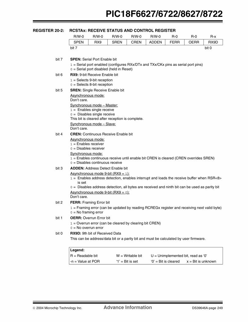
2004 Microchip Technology Inc. Advance Information DS39646A-page 249
PIC18F6627/6722/8627/8722
REGISTER 20-2: RCSTAx: RECEIVE STATUS AND CONTROL REGISTER R/W-0 R/W-0 R/W-0 R/W-0 R/W-0 R-0 R-0 R-x
SPEN RX9 SREN CREN ADDEN FERR OERR RX9D
bit 7 bit 0
bit 7 SPEN: Serial Port Enable bit1 = Serial port enabled (configures RXx/DTx and TXx/CKx pins as serial port pins)0 = Serial port disabled (held in Reset)
bit 6 RX9: 9-bit Receive Enable bit
1 = Selects 9-bit reception 0 = Selects 8-bit reception
bit 5 SREN: Single Receive Enable bit Asynchronous mode: Don’t care.Synchronous mode – Master: 1 = Enables single receive0 = Disables single receive This bit is cleared after reception is complete.
Synchronous mode – Slave: Don’t care.
bit 4 CREN: Continuous Receive Enable bit Asynchronous mode: 1 = Enables receiver0 = Disables receiverSynchronous mode: 1 = Enables continuous receive until enable bit CREN is cleared (CREN overrides SREN) 0 = Disables continuous receive
bit 3 ADDEN: Address Detect Enable bitAsynchronous mode 9-bit (RX9 = 1):1 = Enables address detection, enables interrupt and loads the receive buffer when RSR<8>
is set0 = Disables address detection, all bytes are received and ninth bit can be used as parity bit
Asynchronous mode 9-bit (RX9 = 0):Don’t care.
bit 2 FERR: Framing Error bit 1 = Framing error (can be updated by reading RCREGx register and receiving next valid byte)0 = No framing error
bit 1 OERR: Overrun Error bit 1 = Overrun error (can be cleared by clearing bit CREN) 0 = No overrun error
bit 0 RX9D: 9th bit of Received Data
This can be address/data bit or a parity bit and must be calculated by user firmware.
Legend:
R = Readable bit W = Writable bit U = Unimplemented bit, read as ‘0’
-n = Value at POR ‘1’ = Bit is set ‘0’ = Bit is cleared x = Bit is unknown

PIC18F6627/6722/8627/8722
DS39646A-page 250 Advance Information 2004 Microchip Technology Inc.
REGISTER 20-3: BAUDCONx: BAUD RATE CONTROL REGISTER R/W-0 R-1 U-0 R/W-0 R/W-0 U-0 R/W-0 R/W-0
ABDOVF RCIDL — SCKP BRG16 — WUE ABDEN
bit 7 bit 0
bit 7 ABDOVF: Auto-Baud Acquisition Rollover Status bit1 = A BRG rollover has occurred during Auto-Baud Rate Detect mode
(must be cleared in software)0 = No BRG rollover has occurred
bit 6 RCIDL: Receive Operation Idle Status bit1 = Receive operation is Idle0 = Receive operation is active
bit 5 Unimplemented: Read as ‘0’
bit 4 SCKP: Synchronous Clock Polarity Select bit
Asynchronous mode:Unused in this mode.
Synchronous mode:1 = Idle state for clock (CKx) is a high level0 = Idle state for clock (CKx) is a low level
bit 3 BRG16: 16-bit Baud Rate Register Enable bit1 = 16-bit Baud Rate Generator – SPBRGHx and SPBRGx0 = 8-bit Baud Rate Generator – SPBRGx only (Compatible mode), SPBRGHx value ignored
bit 2 Unimplemented: Read as ‘0’
bit 1 WUE: Wake-up Enable bitAsynchronous mode:1 = EUSART will continue to sample the RXx pin – interrupt generated on falling edge; bit
cleared in hardware on following rising edge0 = RXx pin not monitored or rising edge detected
Synchronous mode:Unused in this mode.
bit 0 ABDEN: Auto-Baud Detect Enable bitAsynchronous mode:1 = Enable baud rate measurement on the next character. Requires reception of a Sync field
(55h); cleared in hardware upon completion0 = Baud rate measurement disabled or completed
Synchronous mode:Unused in this mode.
Legend:
R = Readable bit W = Writable bit U = Unimplemented bit, read as ‘0’
-n = Value at POR ‘1’ = Bit is set ‘0’ = Bit is cleared x = Bit is unknown
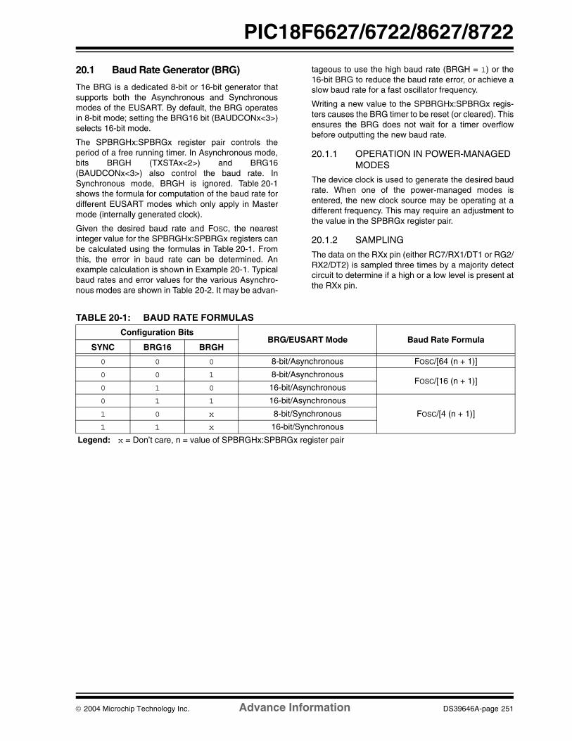
2004 Microchip Technology Inc. Advance Information DS39646A-page 251
PIC18F6627/6722/8627/8722
20.1 Baud Rate Generator (BRG)
The BRG is a dedicated 8-bit or 16-bit generator thatsupports both the Asynchronous and Synchronousmodes of the EUSART. By default, the BRG operatesin 8-bit mode; setting the BRG16 bit (BAUDCONx<3>)selects 16-bit mode.
The SPBRGHx:SPBRGx register pair controls theperiod of a free running timer. In Asynchronous mode,bits BRGH (TXSTAx<2>) and BRG16(BAUDCONx<3>) also control the baud rate. InSynchronous mode, BRGH is ignored. Table 20-1shows the formula for computation of the baud rate fordifferent EUSART modes which only apply in Mastermode (internally generated clock).
Given the desired baud rate and FOSC, the nearestinteger value for the SPBRGHx:SPBRGx registers canbe calculated using the formulas in Table 20-1. Fromthis, the error in baud rate can be determined. Anexample calculation is shown in Example 20-1. Typicalbaud rates and error values for the various Asynchro-nous modes are shown in Table 20-2. It may be advan-
tageous to use the high baud rate (BRGH = 1) or the16-bit BRG to reduce the baud rate error, or achieve aslow baud rate for a fast oscillator frequency.
Writing a new value to the SPBRGHx:SPBRGx regis-ters causes the BRG timer to be reset (or cleared). Thisensures the BRG does not wait for a timer overflowbefore outputting the new baud rate.
20.1.1 OPERATION IN POWER-MANAGED MODES
The device clock is used to generate the desired baudrate. When one of the power-managed modes isentered, the new clock source may be operating at adifferent frequency. This may require an adjustment tothe value in the SPBRGx register pair.
20.1.2 SAMPLING
The data on the RXx pin (either RC7/RX1/DT1 or RG2/RX2/DT2) is sampled three times by a majority detectcircuit to determine if a high or a low level is present atthe RXx pin.
TABLE 20-1: BAUD RATE FORMULAS
Configuration BitsBRG/EUSART Mode Baud Rate Formula
SYNC BRG16 BRGH
0 0 0 8-bit/Asynchronous FOSC/[64 (n + 1)]
0 0 1 8-bit/AsynchronousFOSC/[16 (n + 1)]
0 1 0 16-bit/Asynchronous
0 1 1 16-bit/Asynchronous
FOSC/[4 (n + 1)]1 0 x 8-bit/Synchronous
1 1 x 16-bit/Synchronous
Legend: x = Don’t care, n = value of SPBRGHx:SPBRGx register pair

PIC18F6627/6722/8627/8722
DS39646A-page 252 Advance Information 2004 Microchip Technology Inc.
EXAMPLE 20-1: CALCULATING BAUD RATE ERROR
TABLE 20-2: REGISTERS ASSOCIATED WITH BAUD RATE GENERATOR
For a device with FOSC of 16 MHz, desired baud rate of 9600, Asynchronous mode, 8-bit BRG:Desired Baud Rate = FOSC/(64 ([SPBRGHx:SPBRGx] + 1)) Solving for SPBRGHx:SPBRGx:
X = ((FOSC/Desired Baud Rate)/64) – 1= ((16000000/9600)/64) – 1 = [25.042] = 25
Calculated Baud Rate = 16000000/(64 (25 + 1)) = 9615
Error = (Calculated Baud Rate – Desired Baud Rate)/Desired Baud Rate= (9615 – 9600)/9600 = 0.16%
Name Bit 7 Bit 6 Bit 5 Bit 4 Bit 3 Bit 2 Bit 1 Bit 0Reset Values
on page
TXSTAx CSRC TX9 TXEN SYNC SENDB BRGH TRMT TX9D 59
RCSTAx SPEN RX9 SREN CREN ADDEN FERR OERR RX9D 59
BAUDCONx ABDOVF RCIDL — SCKP BRG16 — WUE ABDEN 61
SPBRGHx EUSART Baud Rate Generator Register, High Byte 59
SPBRGx EUSART Baud Rate Generator Register, Low Byte 59
Legend: — = unimplemented, read as ‘0’. Shaded cells are not used by the BRG.

2004 Microchip Technology Inc. Advance Information DS39646A-page 253
PIC18F6627/6722/8627/8722
TABLE 20-3: BAUD RATES FOR ASYNCHRONOUS MODES
BAUDRATE
(K)
SYNC = 0, BRGH = 0, BRG16 = 0
FOSC = 40.000 MHz FOSC = 20.000 MHz FOSC = 10.000 MHz FOSC = 8.000 MHz
Actual Rate (K)
%Error
SPBRGvalue
(decimal)
Actual Rate (K)
%Error
SPBRGvalue
(decimal)
Actual Rate (K)
%Error
SPBRGvalue
(decimal)
Actual Rate (K)
%Error
SPBRGvalue
(decimal)
0.3 — — — — — — — — — — — —
1.2 — — — 1.221 1.73 255 1.202 0.16 129 1201 -0.16 103
2.4 2.441 1.73 255 2.404 0.16 129 2.404 0.16 64 2403 -0.16 51
9.6 9.615 0.16 64 9.766 1.73 31 9.766 1.73 15 9615 -0.16 12
19.2 19.531 1.73 31 19.531 1.73 15 19.531 1.73 7 — — —
57.6 56.818 -1.36 10 62.500 8.51 4 52.083 -9.58 2 — — —
115.2 125.000 8.51 4 104.167 -9.58 2 78.125 -32.18 1 — — —
BAUDRATE
(K)
SYNC = 0, BRGH = 0, BRG16 = 0
FOSC = 4.000 MHz FOSC = 2.000 MHz FOSC = 1.000 MHz
Actual Rate (K)
%Error
SPBRGvalue
(decimal)
Actual Rate (K)
%Error
SPBRGvalue
(decimal)
Actual Rate (K)
%Error
SPBRGvalue
(decimal)
0.3 0.300 0.16 207 300 -0.16 103 300 -0.16 51
1.2 1.202 0.16 51 1201 -0.16 25 1201 -0.16 12
2.4 2.404 0.16 25 2403 -0.16 12 — — —
9.6 8.929 -6.99 6 — — — — — —
19.2 20.833 8.51 2 — — — — — —
57.6 62.500 8.51 0 — — — — — —
115.2 62.500 -45.75 0 — — — — — —
BAUDRATE
(K)
SYNC = 0, BRGH = 1, BRG16 = 0
FOSC = 40.000 MHz FOSC = 20.000 MHz FOSC = 10.000 MHz FOSC = 8.000 MHz
Actual Rate (K)
%Error
SPBRGvalue
(decimal)
Actual Rate (K)
%Error
SPBRGvalue
(decimal)
Actual Rate (K)
%Error
SPBRGvalue
(decimal)
Actual Rate (K)
%Error
SPBRGvalue
(decimal)
0.3 — — — — — — — — — — — —
1.2 — — — — — — — — — — — —
2.4 — — — — — — 2.441 1.73 255 2403 -0.16 207
9.6 9.766 1.73 255 9.615 0.16 129 9.615 0.16 64 9615 -0.16 51
19.2 19.231 0.16 129 19.231 0.16 64 19.531 1.73 31 19230 -0.16 25
57.6 58.140 0.94 42 56.818 -1.36 21 56.818 -1.36 10 55555 3.55 8
115.2 113.636 -1.36 21 113.636 -1.36 10 125.000 8.51 4 — — —
BAUDRATE
(K)
SYNC = 0, BRGH = 1, BRG16 = 0
FOSC = 4.000 MHz FOSC = 2.000 MHz FOSC = 1.000 MHz
Actual Rate (K)
%Error
SPBRGvalue
(decimal)
Actual Rate (K)
%Error
SPBRGvalue
(decimal)
Actual Rate (K)
%Error
SPBRGvalue
(decimal)
0.3 — — — — — — 300 -0.16 207
1.2 1.202 0.16 207 1201 -0.16 103 1201 -0.16 51
2.4 2.404 0.16 103 2403 -0.16 51 2403 -0.16 25
9.6 9.615 0.16 25 9615 -0.16 12 — — —
19.2 19.231 0.16 12 — — — — — —
57.6 62.500 8.51 3 — — — — — —
115.2 125.000 8.51 1 — — — — — —
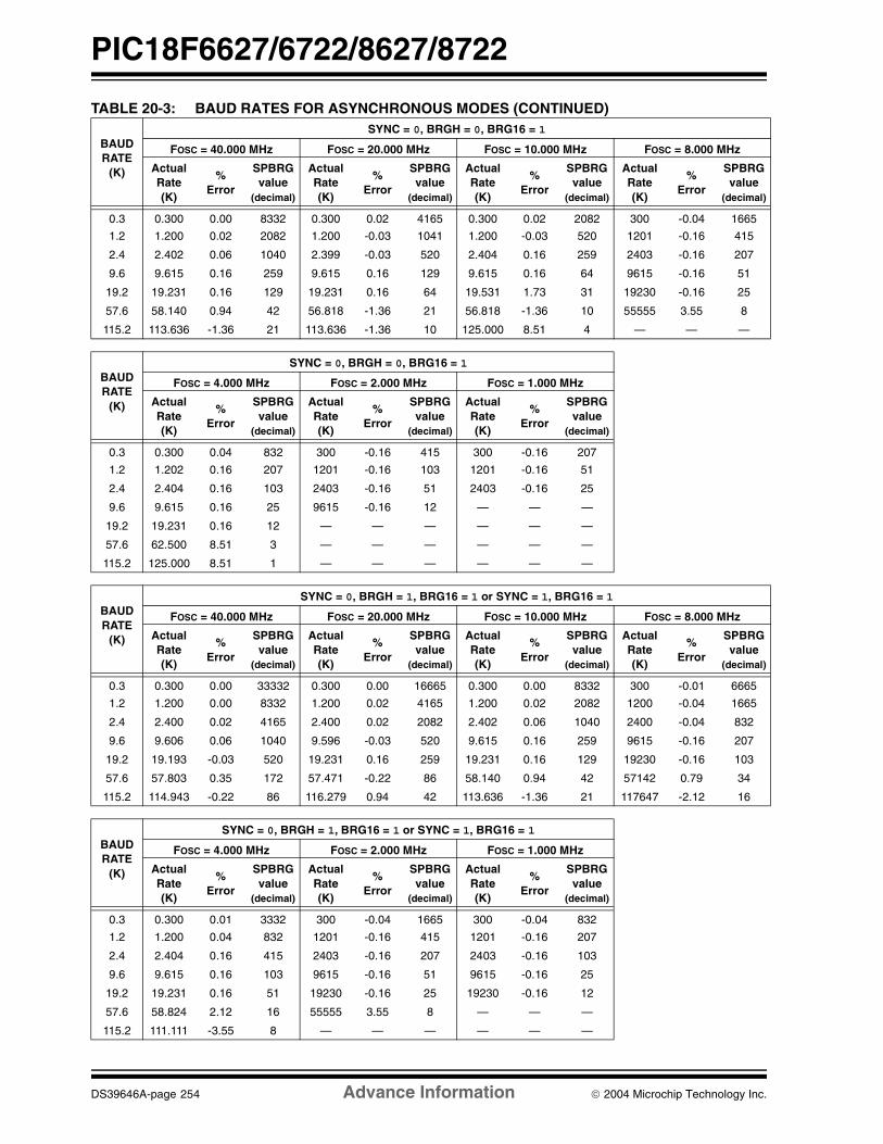
PIC18F6627/6722/8627/8722
DS39646A-page 254 Advance Information 2004 Microchip Technology Inc.
BAUDRATE
(K)
SYNC = 0, BRGH = 0, BRG16 = 1
FOSC = 40.000 MHz FOSC = 20.000 MHz FOSC = 10.000 MHz FOSC = 8.000 MHz
Actual Rate (K)
%Error
SPBRGvalue
(decimal)
Actual Rate (K)
%Error
SPBRGvalue
(decimal)
Actual Rate (K)
%Error
SPBRGvalue
(decimal)
Actual Rate (K)
%Error
SPBRGvalue
(decimal)
0.3 0.300 0.00 8332 0.300 0.02 4165 0.300 0.02 2082 300 -0.04 1665
1.2 1.200 0.02 2082 1.200 -0.03 1041 1.200 -0.03 520 1201 -0.16 415
2.4 2.402 0.06 1040 2.399 -0.03 520 2.404 0.16 259 2403 -0.16 207
9.6 9.615 0.16 259 9.615 0.16 129 9.615 0.16 64 9615 -0.16 51
19.2 19.231 0.16 129 19.231 0.16 64 19.531 1.73 31 19230 -0.16 25
57.6 58.140 0.94 42 56.818 -1.36 21 56.818 -1.36 10 55555 3.55 8
115.2 113.636 -1.36 21 113.636 -1.36 10 125.000 8.51 4 — — —
BAUDRATE
(K)
SYNC = 0, BRGH = 0, BRG16 = 1
FOSC = 4.000 MHz FOSC = 2.000 MHz FOSC = 1.000 MHz
Actual Rate (K)
%Error
SPBRGvalue
(decimal)
Actual Rate (K)
%Error
SPBRGvalue
(decimal)
Actual Rate (K)
%Error
SPBRGvalue
(decimal)
0.3 0.300 0.04 832 300 -0.16 415 300 -0.16 207
1.2 1.202 0.16 207 1201 -0.16 103 1201 -0.16 51
2.4 2.404 0.16 103 2403 -0.16 51 2403 -0.16 25
9.6 9.615 0.16 25 9615 -0.16 12 — — —
19.2 19.231 0.16 12 — — — — — —
57.6 62.500 8.51 3 — — — — — —
115.2 125.000 8.51 1 — — — — — —
BAUDRATE
(K)
SYNC = 0, BRGH = 1, BRG16 = 1 or SYNC = 1, BRG16 = 1
FOSC = 40.000 MHz FOSC = 20.000 MHz FOSC = 10.000 MHz FOSC = 8.000 MHz
Actual Rate (K)
%Error
SPBRGvalue
(decimal)
Actual Rate (K)
%Error
SPBRGvalue
(decimal)
Actual Rate (K)
%Error
SPBRGvalue
(decimal)
Actual Rate (K)
%Error
SPBRGvalue
(decimal)
0.3 0.300 0.00 33332 0.300 0.00 16665 0.300 0.00 8332 300 -0.01 6665
1.2 1.200 0.00 8332 1.200 0.02 4165 1.200 0.02 2082 1200 -0.04 1665
2.4 2.400 0.02 4165 2.400 0.02 2082 2.402 0.06 1040 2400 -0.04 832
9.6 9.606 0.06 1040 9.596 -0.03 520 9.615 0.16 259 9615 -0.16 207
19.2 19.193 -0.03 520 19.231 0.16 259 19.231 0.16 129 19230 -0.16 103
57.6 57.803 0.35 172 57.471 -0.22 86 58.140 0.94 42 57142 0.79 34
115.2 114.943 -0.22 86 116.279 0.94 42 113.636 -1.36 21 117647 -2.12 16
BAUDRATE
(K)
SYNC = 0, BRGH = 1, BRG16 = 1 or SYNC = 1, BRG16 = 1
FOSC = 4.000 MHz FOSC = 2.000 MHz FOSC = 1.000 MHz
Actual Rate (K)
%Error
SPBRGvalue
(decimal)
Actual Rate (K)
%Error
SPBRGvalue
(decimal)
Actual Rate (K)
%Error
SPBRGvalue
(decimal)
0.3 0.300 0.01 3332 300 -0.04 1665 300 -0.04 832
1.2 1.200 0.04 832 1201 -0.16 415 1201 -0.16 207
2.4 2.404 0.16 415 2403 -0.16 207 2403 -0.16 103
9.6 9.615 0.16 103 9615 -0.16 51 9615 -0.16 25
19.2 19.231 0.16 51 19230 -0.16 25 19230 -0.16 12
57.6 58.824 2.12 16 55555 3.55 8 — — —
115.2 111.111 -3.55 8 — — — — — —
TABLE 20-3: BAUD RATES FOR ASYNCHRONOUS MODES (CONTINUED)

2004 Microchip Technology Inc. Advance Information DS39646A-page 255
PIC18F6627/6722/8627/8722
20.1.3 AUTO-BAUD RATE DETECT
The Enhanced USART module supports the automaticdetection and calibration of baud rate. This feature isactive only in Asynchronous mode and while the WUEbit is clear.
The automatic baud rate measurement sequence(Figure 20-1) begins whenever a Start bit is receivedand the ABDEN bit is set. The calculation isself-averaging.
In the Auto-Baud Rate Detect (ABD) mode, the clock tothe BRG is reversed. Rather than the BRG clocking theincoming RX signal, the RX signal is timing the BRG. InABD mode, the internal Baud Rate Generator is usedas a counter to time the bit period of the incoming serialbyte stream.
Once the ABDEN bit is set, the state machine will clearthe BRG and look for a Start bit. The Auto-Baud RateDetect must receive a byte with the value 55h (ASCII“U”, which is also the LIN bus Sync character) in order tocalculate the proper bit rate. The measurement is takenover both a low and a high bit time in order to minimizeany effects caused by asymmetry of the incoming signal.After a Start bit, the SPBRGx begins counting up, usingthe preselected clock source on the first rising edge ofRX. After eight bits on the RXx pin or the fifth rising edge,an accumulated value totalling the proper BRG period isleft in the SPBRGHx:SPBRGx register pair. Once the 5thedge is seen (this should correspond to the Stop bit), theABDEN bit is automatically cleared.
If a rollover of the BRG occurs (an overflow from FFFFhto 0000h), the event is trapped by the ABDOVF statusbit (BAUDCONx<7>). It is set in hardware by BRG roll-overs and can be set or cleared by the user in software.ABD mode remains active after rollover events and theABDEN bit remains set (Figure 20-2).
While calibrating the baud rate period, the BRG regis-ters are clocked at 1/8th the preconfigured clock rate.Note that the BRG clock will be configured by theBRG16 and BRGH bits. Independent of the BRG16 bitsetting, both the SPBRGx and SPBRGHx will be usedas a 16-bit counter. This allows the user to verify thatno carry occurred for 8-bit modes by checking for 00hin the SPBRGHx register. Refer to Table 20-4 forcounter clock rates to the BRG.
While the ABD sequence takes place, the EUSARTstate machine is held in Idle. The RCxIF interrupt is setonce the fifth rising edge on RX is detected. The valuein the RCREGx needs to be read to clear the RCxIFinterrupt. The contents of RCREGx should be dis-carded.
TABLE 20-4: BRG COUNTER CLOCK RATES
20.1.3.1 ABD and EUSART Transmission
Since the BRG clock is reversed during ABD acquisi-tion, the EUSART transmitter cannot be used duringABD. This means that whenever the ABDEN bit is set,TXREGx cannot be written to. Users should alsoensure that ABDEN does not become set during atransmit sequence. Failing to do this may result inunpredictable EUSART operation.
Note 1: If the WUE bit is set with the ABDEN bit,Auto-Baud Rate Detection will occur onthe byte following the Break character.
2: It is up to the user to determine that theincoming character baud rate is within therange of the selected BRG clock source.Some combinations of oscillator frequencyand EUSART baud rates are not possibledue to bit error rates. Overall systemtiming and communication baud ratesmust be taken into consideration whenusing the Auto-Baud Rate Detectionfeature.
BRG16 BRGH BRG Counter Clock
0 0 FOSC/512
0 1 FOSC/128
1 0 FOSC/128
1 1 FOSC/32
Note: During the ABD sequence, SPBRGx andSPBRGHx are both used as a 16-bit counter,independent of BRG16 setting.

PIC18F6627/6722/8627/8722
DS39646A-page 256 Advance Information 2004 Microchip Technology Inc.
FIGURE 20-1: AUTOMATIC BAUD RATE CALCULATION
FIGURE 20-2: BRG OVERFLOW SEQUENCE
BRG Value
RXx pin
ABDEN bit
RCxIF bit
Bit 0 Bit 1
(Interrupt)
ReadRCREGx
BRG Clock
Start
Auto-ClearedSet by User
XXXXh 0000h
Edge #1
Bit 2 Bit 3Edge #2
Bit 4 Bit 5Edge #3
Bit 6 Bit 7Edge #4
Stop Bit
Edge #5
001Ch
Note: The ABD sequence requires the EUSART module to be configured in Asynchronous mode and WUE = 0.
SPBRGx XXXXh 1Ch
SPBRGHx XXXXh 00h
Start Bit 0
XXXXh 0000h 0000h
FFFFh
BRG Clock
ABDEN bit
RXx pin
ABDOVF bit
BRG Value

2004 Microchip Technology Inc. Advance Information DS39646A-page 257
PIC18F6627/6722/8627/8722
20.2 EUSART Asynchronous Mode
The Asynchronous mode of operation is selected byclearing the SYNC bit (TXSTAx<4>). In this mode, theEUSART uses standard Non-Return-to-Zero (NRZ)format (one Start bit, eight or nine data bits and one Stopbit). The most common data format is 8 bits. An on-chipdedicated 8-bit/16-bit Baud Rate Generator can be usedto derive standard baud rate frequencies from theoscillator.
The EUSART transmits and receives the LSb first. TheEUSART’s transmitter and receiver are functionallyindependent, but use the same data format and baudrate. The Baud Rate Generator produces a clock, eitherx16 or x64 of the bit shift rate depending on the BRGHand BRG16 bits (TXSTAx<2> and BAUDCONx<3>).Parity is not supported by the hardware, but can beimplemented in software and stored as the 9th data bit.
When operating in Asynchronous mode, the EUSARTmodule consists of the following important elements:
• Baud Rate Generator• Sampling Circuit• Asynchronous Transmitter• Asynchronous Receiver• Auto-Wake-up on Sync Break Character• 12-bit Break Character Transmit• Auto-Baud Rate Detection
20.2.1 EUSART ASYNCHRONOUS TRANSMITTER
The EUSART transmitter block diagram is shown inFigure 20-3. The heart of the transmitter is the Transmit(Serial) Shift Register (TSR). The Shift register obtainsits data from the Read/Write Transmit Buffer register,TXREGx. The TXREGx register is loaded with data insoftware. The TSR register is not loaded until the Stopbit has been transmitted from the previous load. Assoon as the Stop bit is transmitted, the TSR is loadedwith new data from the TXREGx register (if available).
Once the TXREGx register transfers the data to the TSRregister (occurs in one TCY), the TXREGx register isempty and the TXxIF flag bit (PIR1<4>) is set. This inter-rupt can be enabled or disabled by setting or clearing theinterrupt enable bit, TXxIE (PIE1<4>). TXxIF will be setregardless of the state of TXxIE; it cannot be cleared insoftware. TXxIF is also not cleared immediately uponloading TXREGx, but becomes valid in the secondinstruction cycle following the load instruction. PollingTXxIF immediately following a load of TXREGx will returninvalid results.
While TXxIF indicates the status of the TXREGx regis-ter, another bit, TRMT (TXSTAx<1>), shows the statusof the TSR register. TRMT is a read-only bit which is setwhen the TSR register is empty. No interrupt logic istied to this bit so the user has to poll this bit in order todetermine if the TSR register is empty.
To set up an Asynchronous Transmission:
1. Initialize the SPBRGHx:SPBRGx registers forthe appropriate baud rate. Set or clear theBRGH and BRG16 bits, as required, to achievethe desired baud rate.
2. Enable the asynchronous serial port by clearingbit SYNC and setting bit SPEN.
3. If interrupts are desired, set enable bit TXxIE.4. If 9-bit transmission is desired, set transmit bit
TX9. Can be used as address/data bit.5. Enable the transmission by setting bit TXEN
which will also set bit TXxIF.6. If 9-bit transmission is selected, the ninth bit
should be loaded in bit TX9D.7. Load data to the TXREGx register (starts
transmission).8. If using interrupts, ensure that the GIE and PEIE
bits in the INTCON register (INTCON<7:6>) areset.
Note 1: The TSR register is not mapped in datamemory so it is not available to the user.
2: Flag bit TXxIF is set when enable bitTXEN is set.

PIC18F6627/6722/8627/8722
DS39646A-page 258 Advance Information 2004 Microchip Technology Inc.
FIGURE 20-3: EUSART TRANSMIT BLOCK DIAGRAM
FIGURE 20-4: ASYNCHRONOUS TRANSMISSION
FIGURE 20-5: ASYNCHRONOUS TRANSMISSION (BACK TO BACK)
TXxIFTXxIE
Interrupt
TXEN Baud Rate CLK
SPBRGx
Baud Rate Generator TX9D
MSb LSb
Data Bus
TXREGx Register
TSR Register
(8) 0
TX9
TRMT SPEN
TXx pin
Pin Bufferand Control
8
• • •
SPBRGHxBRG16
Word 1
Word 1Transmit Shift Reg
Start bit bit 0 bit 1 bit 7/8
Write to TXREGx
BRG Output(Shift Clock)
TXx (pin)
TXxIF bit(Transmit Buffer
Reg. Empty Flag)
TRMT bit(Transmit Shift
Reg. Empty Flag)
1 TCY
Stop bit
Word 1
Transmit Shift Reg.
Write to TXREGx
BRG Output(Shift Clock)
TXx (pin)
TXxIF bit(Interrupt Reg. Flag)
TRMT bit(Transmit Shift
Reg. Empty Flag)
Word 1 Word 2
Word 1 Word 2
Stop bit Start bit
Transmit Shift Reg.
Word 1 Word 2
bit 0 bit 1 bit 7/8 bit 0
Note: This timing diagram shows two consecutive transmissions.
1 TCY
1 TCY
Start bit

2004 Microchip Technology Inc. Advance Information DS39646A-page 259
PIC18F6627/6722/8627/8722
TABLE 20-5: REGISTERS ASSOCIATED WITH ASYNCHRONOUS TRANSMISSION
Name Bit 7 Bit 6 Bit 5 Bit 4 Bit 3 Bit 2 Bit 1 Bit 0Reset Values
on page
INTCON GIE/GIEH PEIE/GIEL TMR0IE INT0IE RBIE TMR0IF INT0IF RBIF 57
PIR1 PSPIF ADIF RC1IF TX1IF SSP1IF CCP1IF TMR2IF TMR1IF 60
PIE1 PSPIE ADIE RC1IE TX1IE SSP1IE CCP1IE TMR2IE TMR1IE 60
IPR1 PSPIP ADIP RC1IP TX1IP SSP1IP CCP1IP TMR2IP TMR1IP 60
TRISC PORTC Data Direction Register 60
TRISG — — — Data Direction Control Register for PORTG 60
RCSTAx SPEN RX9 SREN CREN ADDEN FERR OERR RX9D 59
TXREGx EUSART Transmit Register 59
TXSTAx CSRC TX9 TXEN SYNC SENDB BRGH TRMT TX9D 59
BAUDCONx ABDOVF RCIDL — SCKP BRG16 — WUE ABDEN 61
SPBRGHx EUSART Baud Rate Generator Register, High Byte 61
SPBRGx EUSART Baud Rate Generator Register, Low Byte 59
Legend: — = unimplemented locations read as ‘0’. Shaded cells are not used for asynchronous transmission.

PIC18F6627/6722/8627/8722
DS39646A-page 260 Advance Information 2004 Microchip Technology Inc.
20.2.2 EUSART ASYNCHRONOUS RECEIVER
The receiver block diagram is shown in Figure 20-6.The data is received on the RXx pin and drives the datarecovery block. The data recovery block is actually ahigh-speed shifter operating at x16 times the baud rate,whereas the main receive serial shifter operates at thebit rate or at FOSC. This mode would typically be usedin RS-232 systems.
To set up an Asynchronous Reception:
1. Initialize the SPBRGHx:SPBRGx registers forthe appropriate baud rate. Set or clear theBRGH and BRG16 bits, as required, to achievethe desired baud rate.
2. Enable the asynchronous serial port by clearingbit SYNC and setting bit SPEN.
3. If interrupts are desired, set enable bit RCxIE.4. If 9-bit reception is desired, set bit RX9.5. Enable the reception by setting bit CREN.
6. Flag bit, RCxIF, will be set when reception iscomplete and an interrupt will be generated ifenable bit, RCxIE, was set.
7. Read the RCSTAx register to get the 9th bit (ifenabled) and determine if any error occurredduring reception.
8. Read the 8-bit received data by reading theRCREGx register.
9. If any error occurred, clear the error by clearingenable bit CREN.
10. If using interrupts, ensure that the GIE and PEIEbits in the INTCON register (INTCON<7:6>) areset.
20.2.3 SETTING UP 9-BIT MODE WITH ADDRESS DETECT
This mode would typically be used in RS-485 systems.To set up an Asynchronous Reception with AddressDetect Enable:
1. Initialize the SPBRGHx:SPBRGx registers forthe appropriate baud rate. Set or clear theBRGH and BRG16 bits, as required, to achievethe desired baud rate.
2. Enable the asynchronous serial port by clearingthe SYNC bit and setting the SPEN bit.
3. If interrupts are required, set the RCEN bit andselect the desired priority level with the RCxIPbit.
4. Set the RX9 bit to enable 9-bit reception. 5. Set the ADDEN bit to enable address detect.6. Enable reception by setting the CREN bit.
7. The RCxIF bit will be set when reception iscomplete. The interrupt will be Acknowledged ifthe RCxIE and GIE bits are set.
8. Read the RCSTAx register to determine if anyerror occurred during reception, as well as readbit 9 of data (if applicable).
9. Read RCREGx to determine if the device isbeing addressed.
10. If any error occurred, clear the CREN bit. 11. If the device has been addressed, clear the
ADDEN bit to allow all received data into thereceive buffer and interrupt the CPU.
FIGURE 20-6: EUSART RECEIVE BLOCK DIAGRAM
x64 Baud Rate CLK
Baud Rate Generator
RXx
Pin Bufferand Control
SPEN
DataRecovery
CREN OERR FERR
RSR RegisterMSb LSb
RX9D RCREGx RegisterFIFO
Interrupt RCxIF
RCxIE
Data Bus
8
÷ 64
÷ 16or
Stop Start(8) 7 1 0
RX9
• • •SPBRGxSPBRGHxBRG16
or÷ 4

2004 Microchip Technology Inc. Advance Information DS39646A-page 261
PIC18F6627/6722/8627/8722
FIGURE 20-7: ASYNCHRONOUS RECEPTION
TABLE 20-6: REGISTERS ASSOCIATED WITH ASYNCHRONOUS RECEPTION
20.2.4 AUTO-WAKE-UP ON SYNC BREAK CHARACTER
During Sleep mode, all clocks to the EUSART aresuspended. Because of this, the Baud Rate Generatoris inactive and a proper byte reception cannot beperformed. The auto-wake-up feature allows thecontroller to wake-up due to activity on the RXx/DTxline, while the EUSART is operating in Asynchronousmode.
The auto-wake-up feature is enabled by setting theWUE bit (BAUDCONx<1>). Once set, the typicalreceive sequence on RXx/DTx is disabled and theEUSART remains in an Idle state, monitoring for awake-up event independent of the CPU mode. A wake-up event consists of a high-to-low transition on the
RXx/DTx line. (This coincides with the start of a SyncBreak or a Wake-up Signal character for the LIN proto-col.)
Following a wake-up event, the module generates anRCxIF interrupt. The interrupt is generated synchro-nously to the Q clocks in normal operating modes(Figure 20-8) and asynchronously, if the device is inSleep mode (Figure 20-9). The interrupt condition iscleared by reading the RCREGx register.
The WUE bit is automatically cleared once a low-to-high transition is observed on the RX line following thewake-up event. At this point, the EUSART module is inIdle mode and returns to normal operation. This signalsto the user that the Sync Break event is over.
Name Bit 7 Bit 6 Bit 5 Bit 4 Bit 3 Bit 2 Bit 1 Bit 0Reset Values
on page
INTCON GIE/GIEH PEIE/GIEL TMR0IE INT0IE RBIE TMR0IF INT0IF RBIF 57
PIR1 PSPIF ADIF RC1IF TX1IF SSP1IF CCP1IF TMR2IF TMR1IF 60
PIE1 PSPIE ADIE RC1IE TX1IE SSP1IE CCP1IE TMR2IE TMR1IE 60
IPR1 PSPIP ADIP RC1IP TX1IP SSP1IP CCP1IP TMR2IP TMR1IP 60
TRISC PORTC Data Direction Register 60
TRISG — — — Data Direction Control Register for PORTG 60
RCSTAx SPEN RX9 SREN CREN ADDEN FERR OERR RX9D 59
RCREGx EUSART Receive Register 59
TXSTAx CSRC TX9 TXEN SYNC SENDB BRGH TRMT TX9D 59
BAUDCONx ABDOVF RCIDL — SCKP BRG16 — WUE ABDEN 61
SPBRGHx EUSART Baud Rate Generator Register, High Byte 61
SPBRGx EUSART Baud Rate Generator Register, Low Byte 59
Legend: — = unimplemented locations read as ‘0’. Shaded cells are not used for asynchronous reception.
Startbit bit 7/8bit 1bit 0 bit 7/8 bit 0Stop
bit
Startbit
Startbitbit 7/8 Stop
bit
RXx (pin)
Rcv Buffer RegRcv Shift Reg
Read RcvBuffer RegRCREGx
RCxIF(Interrupt Flag)
OERR bit
CREN
Word 1RCREGx
Word 2RCREGx
Stopbit
Note: This timing diagram shows three words appearing on the RX input. The RCREGx (receive buffer) is read after the third wordcausing the OERR (overrun) bit to be set.

PIC18F6627/6722/8627/8722
DS39646A-page 262 Advance Information 2004 Microchip Technology Inc.
20.2.4.1 Special Considerations Using Auto-Wake-up
Since auto-wake-up functions by sensing rising edgetransitions on RXx/DTx, information with any statechanges before the Stop bit may signal a false end-of-character and cause data or framing errors. To workproperly, therefore, the initial character in the transmis-sion must be all ‘0’s. This can be 00h (8 bytes) forstandard RS-232 devices or 000h (12 bits) for LIN bus.
Oscillator start-up time must also be considered,especially in applications using oscillators with longerstart-up intervals (i.e., XT or HS mode). The SyncBreak (or Wake-up Signal) character must be ofsufficient length and be followed by a sufficient intervalto allow enough time for the selected oscillator to startand provide proper initialization of the EUSART.
20.2.4.2 Special Considerations Using the WUE Bit
The timing of WUE and RCxIF events may causesome confusion when it comes to determining thevalidity of received data. As noted, setting the WUE bitplaces the EUSART in an Idle mode. The wake-upevent causes a receive interrupt by setting the RCxIFbit. The WUE bit is cleared after this when a risingedge is seen on RXx/DTx. The interrupt condition isthen cleared by reading the RCREGx register.Ordinarily, the data in RCREGx will be dummy dataand should be discarded.
The fact that the WUE bit has been cleared (or is stillset) and the RCxIF flag is set should not be used as anindicator of the integrity of the data in RCREGx. Usersshould consider implementing a parallel method infirmware to verify received data integrity.
To assure that no actual data is lost, check the RCIDLbit to verify that a receive operation is not in process. Ifa receive operation is not occurring, the WUE bit maythen be set just prior to entering the Sleep mode.
FIGURE 20-8: AUTO-WAKE-UP BIT (WUE) TIMINGS DURING NORMAL OPERATION
FIGURE 20-9: AUTO-WAKE-UP BIT (WUE) TIMINGS DURING SLEEP
Q1 Q2 Q3 Q4 Q1 Q2 Q3 Q4 Q1 Q2 Q3 Q4 Q1 Q2 Q3 Q4 Q1 Q2 Q3 Q4 Q1 Q2 Q3 Q4 Q1 Q2 Q3 Q4 Q1 Q2 Q3 Q4 Q1 Q2 Q3 Q4 Q1 Q2 Q3 Q4
OSC1
WUE bit(1)
RXx/DTx Line
RCxIF
Note 1: The EUSART remains in Idle while the WUE bit is set.
Bit set by user
Cleared due to user read of RCREGx
Auto-Cleared
Q1 Q2 Q3 Q4 Q1 Q2 Q3 Q4 Q1 Q2 Q3 Q4 Q1 Q2 Q3 Q4 Q1 Q2 Q3 Q4 Q1 Q2 Q3 Q4 Q1 Q2 Q3 Q4 Q1 Q2 Q3 Q4
OSC1
WUE bit(2)
RXx/DTx Line
RCxIF
Bit set by user
Cleared due to user read of RCREGxSleep Command Executed
Note 1: If the wake-up event requires long oscillator warm-up time, the auto-clear of the WUE bit can occur before the oscillator is ready. Thissequence should not depend on the presence of Q clocks.
2: The EUSART remains in Idle while the WUE bit is set.
Sleep Ends
Note 1
Auto-Cleared

2004 Microchip Technology Inc. Advance Information DS39646A-page 263
PIC18F6627/6722/8627/8722
20.2.5 BREAK CHARACTER SEQUENCE
The EUSART module has the capability of sending thespecial Break character sequences that are required bythe LIN bus standard. The Break character transmitconsists of a Start bit, followed by twelve ‘0’ bits and aStop bit. The frame Break character is sent wheneverthe SENDB and TXEN bits (TXSTAx<3> andTXSTAx<5>) are set while the Transmit Shift register isloaded with data. Note that the value of data written toTXREGx will be ignored and all ‘0’s will be transmitted.
The SENDB bit is automatically reset by hardware afterthe corresponding Stop bit is sent. This allows the userto preload the transmit FIFO with the next transmit bytefollowing the Break character (typically, the Synccharacter in the LIN specification).
Note that the data value written to the TXREGx for theBreak character is ignored. The write simply serves thepurpose of initiating the proper sequence.
The TRMT bit indicates when the transmit operation isactive or Idle, just as it does during normal transmis-sion. See Figure 20-10 for the timing of the Breakcharacter sequence.
20.2.5.1 Break and Sync Transmit Sequence
The following sequence will send a message frameheader made up of a Break, followed by an Auto-BaudSync byte. This sequence is typical of a LIN busmaster.
1. Configure the EUSART for the desired mode.2. Set the TXEN and SENDB bits to set up the
Break character.3. Load the TXREGx with a dummy character to
initiate transmission (the value is ignored).4. Write ‘55h’ to TXREGx to load the Sync
character into the transmit FIFO buffer.5. After the Break has been sent, the SENDB bit is
reset by hardware. The Sync character nowtransmits in the preconfigured mode.
When the TXREGx becomes empty, as indicated bythe TXxIF, the next data byte can be written toTXREGx.
20.2.6 RECEIVING A BREAK CHARACTER
The enhanced USART module can receive a Breakcharacter in two ways.
The first method forces configuration of the baud rateat a frequency of 9/13 the typical speed. This allows forthe Stop bit transition to be at the correct sampling loca-tion (13 bits for Break versus Start bit and 8 data bits fortypical data).
The second method uses the auto-wake-up featuredescribed in Section 20.2.4 “Auto-Wake-up on SyncBreak Character”. By enabling this feature, theEUSART will sample the next two transitions on RXx/DTx, cause an RCxIF interrupt and receive the nextdata byte followed by another interrupt.
Note that following a Break character, the user willtypically want to enable the Auto-Baud Rate Detectfeature. For both methods, the user can set the ABD bitonce the TXxIF interrupt is observed.
FIGURE 20-10: SEND BREAK CHARACTER SEQUENCE
Write to TXREGx
BRG Output(Shift Clock)
Start Bit Bit 0 Bit 1 Bit 11 Stop Bit
Break
TXxIF bit(Transmit Buffer
Reg. Empty Flag)
TXx (pin)
TRMT bit(Transmit Shift
Reg. Empty Flag)
SENDB(Transmit Shift
Reg. Empty Flag)
SENDB sampled here Auto-Cleared
Dummy Write

PIC18F6627/6722/8627/8722
DS39646A-page 264 Advance Information 2004 Microchip Technology Inc.
20.3 EUSART Synchronous Master Mode
The Synchronous Master mode is entered by settingthe CSRC bit (TXSTAx<7>). In this mode, the data istransmitted in a half-duplex manner (i.e., transmissionand reception do not occur at the same time). Whentransmitting data, the reception is inhibited and viceversa. Synchronous mode is entered by setting bitSYNC (TXSTAx<4>). In addition, enable bit SPEN(RCSTAx<7>) is set in order to configure the TXx andRXx pins to CK (clock) and DT (data) lines,respectively.
The Master mode indicates that the processor trans-mits the master clock on the CKx line. Clock polarity isselected with the SCKP bit (BAUDCONx<4>); settingSCKP sets the Idle state on CK as high, while clearingthe bit sets the Idle state as low. This option is providedto support Microwire devices with this module.
20.3.1 EUSART SYNCHRONOUS MASTER TRANSMISSION
The EUSART transmitter block diagram is shown inFigure 20-3. The heart of the transmitter is the Transmit(Serial) Shift Register (TSR). The Shift register obtainsits data from the Read/Write Transmit Buffer register,TXREGx. The TXREGx register is loaded with data insoftware. The TSR register is not loaded until the lastbit has been transmitted from the previous load. Assoon as the last bit is transmitted, the TSR is loadedwith new data from the TXREGx (if available).
Once the TXREGx register transfers the data to theTSR register (occurs in one TCY), the TXREGx is emptyand the TXxIF flag bit is set. The interrupt can beenabled or disabled by setting or clearing the interruptenable bit, TXxIE. TXxIF is set regardless of the stateof enable bit TXxIE; it cannot be cleared in software. Itwill reset only when new data is loaded into theTXREGx register.
While flag bit TXxIF indicates the status of the TXREGxregister, another bit, TRMT (TXSTAx<1>), shows thestatus of the TSR register. TRMT is a read-only bit whichis set when the TSR is empty. No interrupt logic is tied tothis bit, so the user must poll this bit in order to determineif the TSR register is empty. The TSR is not mapped indata memory so it is not available to the user.
To set up a Synchronous Master Transmission:
1. Initialize the SPBRGHx:SPBRGx registers for theappropriate baud rate. Set or clear the BRG16bit, as required, to achieve the desired baud rate.
2. Enable the synchronous master serial port bysetting bits SYNC, SPEN and CSRC.
3. If interrupts are desired, set enable bit TXxIE.
4. If 9-bit transmission is desired, set bit TX9.5. Enable the transmission by setting bit TXEN.6. If 9-bit transmission is selected, the ninth bit
should be loaded in bit TX9D.7. Start transmission by loading data to the
TXREGx register.8. If using interrupts, ensure that the GIE and PEIE
bits in the INTCON register (INTCON<7:6>) areset.
FIGURE 20-11: SYNCHRONOUS TRANSMISSION
bit 0 bit 1 bit 7
Word 1
Q1 Q2 Q3Q4 Q1 Q2 Q3 Q4 Q1Q2 Q3 Q4 Q1Q2 Q3 Q4 Q1 Q2 Q3 Q4 Q3 Q4 Q1 Q2 Q3Q4 Q1Q2 Q3Q4 Q1 Q2Q3Q4 Q1 Q2Q3 Q4Q1 Q2 Q3 Q4 Q1 Q2 Q3 Q4
bit 2 bit 0 bit 1 bit 7RC7/RXx/DTx
RC6/TXx/CKx pin
Write toTXREGx Reg
TXxIF bit(Interrupt Flag)
TXEN bit ‘1’ ‘1’
Word 2
TRMT bit
Write Word 1 Write Word 2
Note: Sync Master mode, SPBRGx = 0, continuous transmission of two 8-bit words.
RC6/TXx/CKx pin(SCKP = 0)
(SCKP = 1)
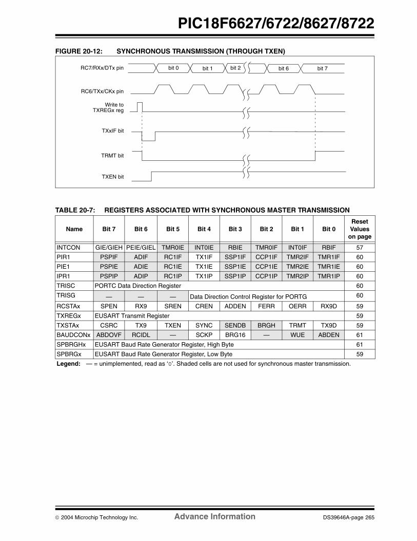
2004 Microchip Technology Inc. Advance Information DS39646A-page 265
PIC18F6627/6722/8627/8722
FIGURE 20-12: SYNCHRONOUS TRANSMISSION (THROUGH TXEN)
TABLE 20-7: REGISTERS ASSOCIATED WITH SYNCHRONOUS MASTER TRANSMISSION
RC7/RXx/DTx pin
RC6/TXx/CKx pin
Write toTXREGx reg
TXxIF bit
TRMT bit
bit 0 bit 1 bit 2 bit 6 bit 7
TXEN bit
Name Bit 7 Bit 6 Bit 5 Bit 4 Bit 3 Bit 2 Bit 1 Bit 0Reset Values
on page
INTCON GIE/GIEH PEIE/GIEL TMR0IE INT0IE RBIE TMR0IF INT0IF RBIF 57
PIR1 PSPIF ADIF RC1IF TX1IF SSP1IF CCP1IF TMR2IF TMR1IF 60
PIE1 PSPIE ADIE RC1IE TX1IE SSP1IE CCP1IE TMR2IE TMR1IE 60
IPR1 PSPIP ADIP RC1IP TX1IP SSP1IP CCP1IP TMR2IP TMR1IP 60
TRISC PORTC Data Direction Register 60
TRISG — — — Data Direction Control Register for PORTG 60
RCSTAx SPEN RX9 SREN CREN ADDEN FERR OERR RX9D 59
TXREGx EUSART Transmit Register 59
TXSTAx CSRC TX9 TXEN SYNC SENDB BRGH TRMT TX9D 59
BAUDCONx ABDOVF RCIDL — SCKP BRG16 — WUE ABDEN 61
SPBRGHx EUSART Baud Rate Generator Register, High Byte 61
SPBRGx EUSART Baud Rate Generator Register, Low Byte 59
Legend: — = unimplemented, read as ‘0’. Shaded cells are not used for synchronous master transmission.

PIC18F6627/6722/8627/8722
DS39646A-page 266 Advance Information 2004 Microchip Technology Inc.
20.3.2 EUSART SYNCHRONOUS MASTER RECEPTION
Once Synchronous mode is selected, reception isenabled by setting either the Single Receive Enable bit,SREN (RCSTAx<5>), or the Continuous ReceiveEnable bit, CREN (RCSTAx<4>). Data is sampled onthe RXx pin on the falling edge of the clock.
If enable bit SREN is set, only a single word is received.If enable bit CREN is set, the reception is continuousuntil CREN is cleared. If both bits are set, then CRENtakes precedence.
To set up a Synchronous Master Reception:
1. Initialize the SPBRGHx:SPBRGx registers for theappropriate baud rate. Set or clear the BRG16bit, as required, to achieve the desired baud rate.
2. Enable the synchronous master serial port bysetting bits SYNC, SPEN and CSRC.
3. Ensure bits CREN and SREN are clear.4. If interrupts are desired, set enable bit RCxIE.5. If 9-bit reception is desired, set bit RX9.6. If a single reception is required, set bit SREN.
For continuous reception, set bit CREN.7. Interrupt flag bit, RCxIF, will be set when recep-
tion is complete and an interrupt will be generatedif the enable bit, RCxIE, was set.
8. Read the RCSTAx register to get the 9th bit (ifenabled) and determine if any error occurredduring reception.
9. Read the 8-bit received data by reading theRCREGx register.
10. If any error occurred, clear the error by clearingbit CREN.
11. If using interrupts, ensure that the GIE and PEIE bitsin the INTCON register (INTCON<7:6>) are set.
FIGURE 20-13: SYNCHRONOUS RECEPTION (MASTER MODE, SREN)
TABLE 20-8: REGISTERS ASSOCIATED WITH SYNCHRONOUS MASTER RECEPTION
Name Bit 7 Bit 6 Bit 5 Bit 4 Bit 3 Bit 2 Bit 1 Bit 0Reset
Values on page
INTCON GIE/GIEH PEIE/GIEL TMR0IE INT0IE RBIE TMR0IF INT0IF RBIF 57
PIR1 PSPIF ADIF RC1IF TX1IF SSP1IF CCP1IF TMR2IF TMR1IF 60
PIE1 PSPIE ADIE RC1IE TX1IE SSP1IE CCP1IE TMR2IE TMR1IE 60
IPR1 PSPIP ADIP RC1IP TX1IP SSP1IP CCP1IP TMR2IP TMR1IP 60
TRISC PORTC Data Direction Register 60
TRISG — — — Data Direction Control Register for PORTG 60
RCSTAx SPEN RX9 SREN CREN ADDEN FERR OERR RX9D 59
RCREGx EUSART Receive Register 59
TXSTAx CSRC TX9 TXEN SYNC SENDB BRGH TRMT TX9D 59
BAUDCONx ABDOVF RCIDL — SCKP BRG16 — WUE ABDEN 61
SPBRGHx EUSART Baud Rate Generator Register, High Byte 61
SPBRGx EUSART Baud Rate Generator Register, Low Byte 59
Legend: — = unimplemented, read as ‘0’. Shaded cells are not used for synchronous master reception.
CREN bit
RC7/RXx/DTx
RC6/TXx/CKx pin
Write tobit SREN
SREN bit
RCxIF bit(Interrupt)
ReadRXREG
Q3 Q4 Q1 Q2 Q3 Q4 Q1 Q2 Q3 Q4Q2 Q1 Q2 Q3 Q4 Q1 Q2 Q3 Q4 Q1 Q2 Q3 Q4 Q1 Q2 Q3 Q4 Q1Q2 Q3 Q4 Q1 Q2 Q3 Q4 Q1 Q2 Q3 Q4
‘0’
bit 0 bit 1 bit 2 bit 3 bit 4 bit 5 bit 6 bit 7
‘0’
Q1 Q2 Q3 Q4
Note: Timing diagram demonstrates Sync Master mode with bit SREN = 1 and bit BRGH = 0.
RC6/TXx/CKx pin
pin
(SCKP = 0)
(SCKP = 1)

2004 Microchip Technology Inc. Advance Information DS39646A-page 267
PIC18F6627/6722/8627/8722
20.4 EUSART Synchronous Slave Mode
Synchronous Slave mode is entered by clearing bit,CSRC (TXSTAx<7>). This mode differs from theSynchronous Master mode in that the shift clock issupplied externally at the CKx pin (instead of beingsupplied internally in Master mode). This allows thedevice to transfer or receive data while in any low-power mode.
20.4.1 EUSART SYNCHRONOUS SLAVE TRANSMISSION
The operation of the Synchronous Master and Slavemodes are identical, except in the case of the Sleepmode.
If two words are written to the TXREGx and then theSLEEP instruction is executed, the following will occur:
a) The first word will immediately transfer to theTSR register and transmit.
b) The second word will remain in the TXREGxregister.
c) Flag bit, TXxIF, will not be set. d) When the first word has been shifted out of TSR,
the TXREGx register will transfer the secondword to the TSR and flag bit, TXxIF, will now beset.
e) If enable bit TXxIE is set, the interrupt will wakethe chip from Sleep. If the global interrupt isenabled, the program will branch to the interruptvector.
To set up a Synchronous Slave Transmission:
1. Enable the synchronous slave serial port bysetting bits SYNC and SPEN and clearing bitCSRC.
2. Clear bits CREN and SREN.3. If interrupts are desired, set enable bit TXxIE.4. If 9-bit transmission is desired, set bit TX9.
5. Enable the transmission by setting enable bitTXEN.
6. If 9-bit transmission is selected, the ninth bitshould be loaded in bit TX9D.
7. Start transmission by loading data to theTXREGx register.
8. If using interrupts, ensure that the GIE and PEIEbits in the INTCON register (INTCON<7:6>) areset.
TABLE 20-9: REGISTERS ASSOCIATED WITH SYNCHRONOUS SLAVE TRANSMISSION
Name Bit 7 Bit 6 Bit 5 Bit 4 Bit 3 Bit 2 Bit 1 Bit 0Reset Values
on page
INTCON GIE/GIEH PEIE/GIEL TMR0IE INT0IE RBIE TMR0IF INT0IF RBIF 57
PIR1 PSPIF ADIF RC1IF TX1IF SSP1IF CCP1IF TMR2IF TMR1IF 60
PIE1 PSPIE ADIE RC1IE TX1IE SSP1IE CCP1IE TMR2IE TMR1IE 60
IPR1 PSPIP ADIP RC1IP TX1IP SSP1IP CCP1IP TMR2IP TMR1IP 60
TRISC PORTC Data Direction Register 60
TRISG — — — Data Direction Control Register for PORTG 60
RCSTAx SPEN RX9 SREN CREN ADDEN FERR OERR RX9D 59
TXREGx EUSART Transmit Register 59
TXSTAx CSRC TX9 TXEN SYNC SENDB BRGH TRMT TX9D 59
BAUDCONx ABDOVF RCIDL — SCKP BRG16 — WUE ABDEN 61
SPBRGHx EUSART Baud Rate Generator Register, High Byte 61
SPBRGx EUSART Baud Rate Generator Register, Low Byte 59
Legend: — = unimplemented, read as ‘0’. Shaded cells are not used for synchronous slave transmission.

PIC18F6627/6722/8627/8722
DS39646A-page 268 Advance Information 2004 Microchip Technology Inc.
20.4.2 EUSART SYNCHRONOUS SLAVE RECEPTION
The operation of the Synchronous Master and Slavemodes is identical, except in the case of Sleep, or anyIdle mode and bit SREN, which is a “don’t care” inSlave mode.
If receive is enabled by setting the CREN bit prior toentering Sleep or any Idle mode, then a word may bereceived while in this low-power mode. Once the wordis received, the RSR register will transfer the data to theRCREGx register; if the RCxIE enable bit is set, theinterrupt generated will wake the chip from the low-power mode. If the global interrupt is enabled, theprogram will branch to the interrupt vector.
To set up a Synchronous Slave Reception:
1. Enable the synchronous master serial port bysetting bits SYNC and SPEN and clearing bitCSRC.
2. If interrupts are desired, set enable bit RCxIE.3. If 9-bit reception is desired, set bit RX9.4. To enable reception, set enable bit CREN.
5. Flag bit, RCxIF, will be set when reception iscomplete. An interrupt will be generated ifenable bit, RCxIE, was set.
6. Read the RCSTAx register to get the 9th bit (ifenabled) and determine if any error occurredduring reception.
7. Read the 8-bit received data by reading theRCREGx register.
8. If any error occurred, clear the error by clearingbit CREN.
9. If using interrupts, ensure that the GIE and PEIEbits in the INTCON register (INTCON<7:6>) areset.
TABLE 20-10: REGISTERS ASSOCIATED WITH SYNCHRONOUS SLAVE RECEPTION
Name Bit 7 Bit 6 Bit 5 Bit 4 Bit 3 Bit 2 Bit 1 Bit 0Reset Values
on page
INTCON GIE/GIEH PEIE/GIEL TMR0IE INT0IE RBIE TMR0IF INT0IF RBIF 57
PIR1 PSPIF ADIF RC1IF TX1IF SSP1IF CCP1IF TMR2IF TMR1IF 60
PIE1 PSPIE ADIE RC1IE TX1IE SSP1IE CCP1IE TMR2IE TMR1IE 60
IPR1 PSPIP ADIP RC1IP TX1IP SSP1IP CCP1IP TMR2IP TMR1IP 60
TRISC PORTC Data Direction Register 60
TRISG — — — Data Direction Control Register for PORTG 60
RCSTAx SPEN RX9 SREN CREN ADDEN FERR OERR RX9D 59
RCREGx EUSART Receive Register 59
TXSTAx CSRC TX9 TXEN SYNC SENDB BRGH TRMT TX9D 59
BAUDCONx ABDOVF RCIDL — SCKP BRG16 — WUE ABDEN 61
SPBRGHx EUSART Baud Rate Generator Register, High Byte 61
SPBRGx EUSART Baud Rate Generator Register, Low Byte 59
Legend: — = unimplemented, read as ‘0’. Shaded cells are not used for synchronous slave reception.

2004 Microchip Technology Inc. Advance Information DS39646A-page 269
PIC18F6627/6722/8627/8722
21.0 10-BIT ANALOG-TO-DIGITAL CONVERTER (A/D) MODULE
The Analog-to-Digital (A/D) converter module has12 inputs for the 64-pin devices and 16 for the 80-pindevices. This module allows conversion of an analoginput signal to a corresponding 10-bit digital number.
The module has five registers:
• A/D Result High Register (ADRESH)
• A/D Result Low Register (ADRESL)• A/D Control Register 0 (ADCON0)• A/D Control Register 1 (ADCON1)
• A/D Control Register 2 (ADCON2)
The ADCON0 register, shown in Register 21-1,controls the operation of the A/D module. TheADCON1 register, shown in Register 21-2, configuresthe functions of the port pins. The ADCON2 register,shown in Register 21-3, configures the A/D clocksource, programmed acquisition time and justification.
REGISTER 21-1: ADCON0: A/D CONTROL REGISTER U-0 U-0 R/W-0 R/W-0 R/W-0 R/W-0 R/W-0 R/W-0
— — CHS3 CHS2 CHS1 CHS0 GO/DONE ADON
bit 7 bit 0
bit 7-6 Unimplemented: Read as ‘0’
bit 5-2 CHS3:CHS0: Analog Channel Select bits0000 = Channel 0 (AN0)0001 = Channel 1 (AN1)0010 = Channel 2 (AN2)0011 = Channel 3 (AN3)0100 = Channel 4 (AN4)0101 = Channel 5 (AN5)0110 = Channel 6 (AN6)0111 = Channel 7 (AN7)1000 = Channel 8 (AN8)1001 = Channel 9 (AN9)1010 = Channel 10 (AN10)1011 = Channel 11 (AN11)1100 = Channel 12 (AN12)(1)
1101 = Channel 13 (AN13)(1)
1110 = Channel 14 (AN14)(1)
1111 = Channel 15 (AN15)(1)
Note 1: These channels are not implemented on 64-pin devices.
bit 1 GO/DONE: A/D Conversion Status bitWhen ADON = 1: 1 = A/D conversion in progress0 = A/D Idle
bit 0 ADON: A/D On bit1 = A/D converter module is enabled 0 = A/D converter module is disabled
Legend:
R = Readable bit W = Writable bit U = Unimplemented bit, read as ‘0’
-n = Value at POR ‘1’ = Bit is set ‘0’ = Bit is cleared x = Bit is unknown
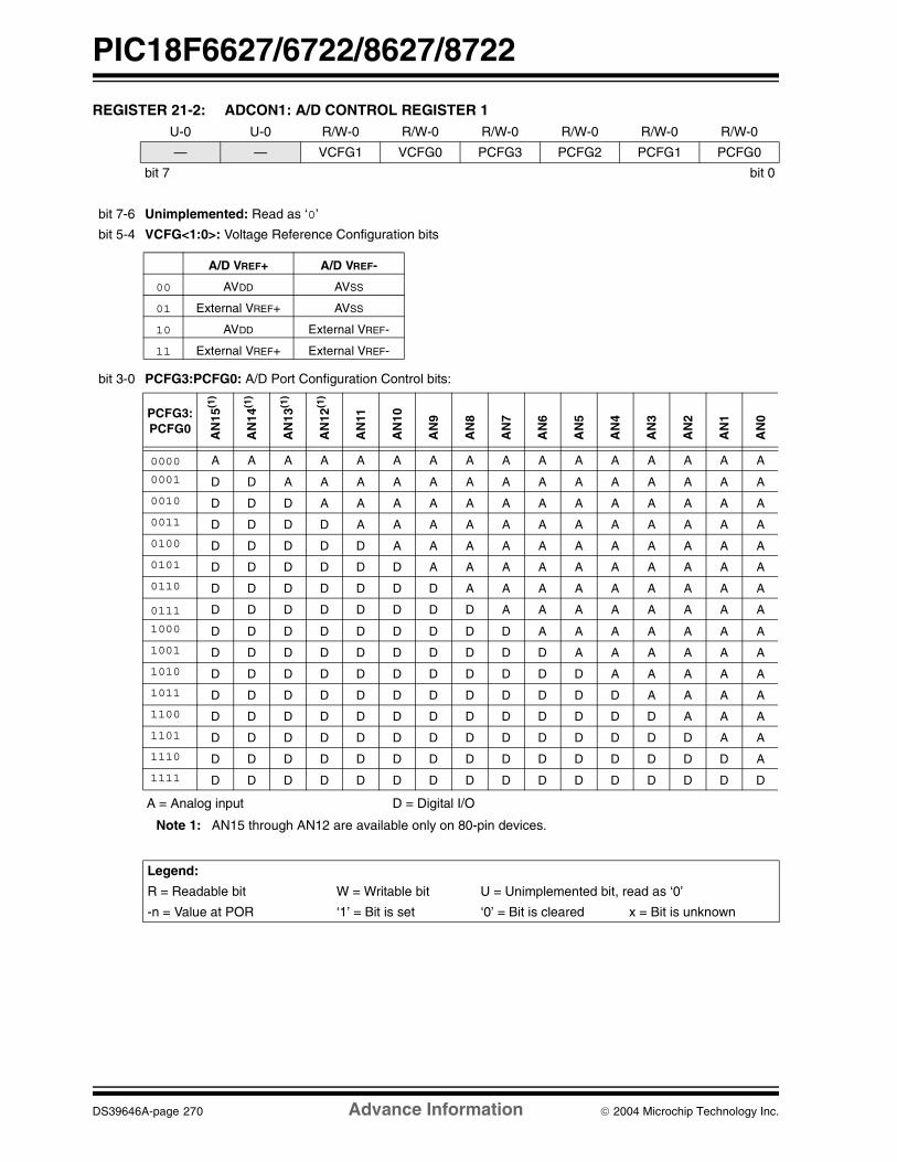
PIC18F6627/6722/8627/8722
DS39646A-page 270 Advance Information 2004 Microchip Technology Inc.
REGISTER 21-2: ADCON1: A/D CONTROL REGISTER 1 U-0 U-0 R/W-0 R/W-0 R/W-0 R/W-0 R/W-0 R/W-0
— — VCFG1 VCFG0 PCFG3 PCFG2 PCFG1 PCFG0
bit 7 bit 0
bit 7-6 Unimplemented: Read as ‘0’
bit 5-4 VCFG<1:0>: Voltage Reference Configuration bits
bit 3-0 PCFG3:PCFG0: A/D Port Configuration Control bits:
Legend:
R = Readable bit W = Writable bit U = Unimplemented bit, read as ‘0’
-n = Value at POR ‘1’ = Bit is set ‘0’ = Bit is cleared x = Bit is unknown
A/D VREF+ A/D VREF-
00 AVDD AVSS
01 External VREF+ AVSS
10 AVDD External VREF-
11 External VREF+ External VREF-
A = Analog input D = Digital I/O
Note 1: AN15 through AN12 are available only on 80-pin devices.
PCFG3:PCFG0 A
N15
(1)
AN
14(1
)
AN
13(1
)
AN
12(1
)
AN
11
AN
10
AN
9
AN
8
AN
7
AN
6
AN
5
AN
4
AN
3
AN
2
AN
1
AN
0
0000 A A A A A A A A A A A A A A A A
0001 D D A A A A A A A A A A A A A A
0010 D D D A A A A A A A A A A A A A
0011 D D D D A A A A A A A A A A A A
0100 D D D D D A A A A A A A A A A A
0101 D D D D D D A A A A A A A A A A
0110 D D D D D D D A A A A A A A A A
0111 D D D D D D D D A A A A A A A A
1000 D D D D D D D D D A A A A A A A
1001 D D D D D D D D D D A A A A A A
1010 D D D D D D D D D D D A A A A A
1011 D D D D D D D D D D D D A A A A
1100 D D D D D D D D D D D D D A A A
1101 D D D D D D D D D D D D D D A A
1110 D D D D D D D D D D D D D D D A
1111 D D D D D D D D D D D D D D D D
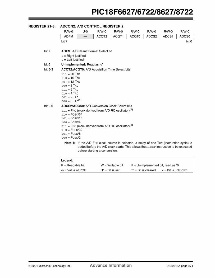
2004 Microchip Technology Inc. Advance Information DS39646A-page 271
PIC18F6627/6722/8627/8722
REGISTER 21-3: ADCON2: A/D CONTROL REGISTER 2 R/W-0 U-0 R/W-0 R/W-0 R/W-0 R/W-0 R/W-0 R/W-0
ADFM — ACQT2 ACQT1 ACQT0 ADCS2 ADCS1 ADCS0
bit 7 bit 0
bit 7 ADFM: A/D Result Format Select bit1 = Right justified 0 = Left justified
bit 6 Unimplemented: Read as ‘0’
bit 5-3 ACQT2:ACQT0: A/D Acquisition Time Select bits111 = 20 TAD
110 = 16 TAD
101 = 12 TAD
100 = 8 TAD
011 = 6 TAD
010 = 4 TAD
001 = 2 TAD
000 = 0 TAD(1)
bit 2-0 ADCS2:ADCS0: A/D Conversion Clock Select bits111 = FRC (clock derived from A/D RC oscillator)(1) 110 = FOSC/64 101 = FOSC/16 100 = FOSC/4 011 = FRC (clock derived from A/D RC oscillator)(1) 010 = FOSC/32 001 = FOSC/8 000 = FOSC/2
Note 1: If the A/D FRC clock source is selected, a delay of one TCY (instruction cycle) isadded before the A/D clock starts. This allows the SLEEP instruction to be executedbefore starting a conversion.
Legend:
R = Readable bit W = Writable bit U = Unimplemented bit, read as ‘0’
-n = Value at POR ‘1’ = Bit is set ‘0’ = Bit is cleared x = Bit is unknown
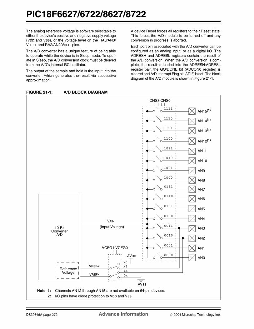
PIC18F6627/6722/8627/8722
DS39646A-page 272 Advance Information 2004 Microchip Technology Inc.
The analog reference voltage is software selectable toeither the device’s positive and negative supply voltage(VDD and VSS), or the voltage level on the RA3/AN3/VREF+ and RA2/AN2/VREF- pins.
The A/D converter has a unique feature of being ableto operate while the device is in Sleep mode. To oper-ate in Sleep, the A/D conversion clock must be derivedfrom the A/D’s internal RC oscillator.
The output of the sample and hold is the input into theconverter, which generates the result via successiveapproximation.
A device Reset forces all registers to their Reset state.This forces the A/D module to be turned off and anyconversion in progress is aborted.
Each port pin associated with the A/D converter can beconfigured as an analog input, or as a digital I/O. TheADRESH and ADRESL registers contain the result ofthe A/D conversion. When the A/D conversion is com-plete, the result is loaded into the ADRESH:ADRESLregister pair, the GO/DONE bit (ADCON0 register) iscleared and A/D Interrupt Flag bit, ADIF, is set. The blockdiagram of the A/D module is shown in Figure 21-1.
FIGURE 21-1: A/D BLOCK DIAGRAM
(Input Voltage)
VAIN
VREF+Reference
Voltage
AVDD
VCFG1:VCFG0
CHS3:CHS0
AN7
AN6
AN5
AN4
AN3
AN2
AN1
AN0
0111
0110
0101
0100
0011
0010
0001
0000
10-BitConverter
VREF-
AVSS
A/D
AN12(1)
AN11
AN10
AN9
AN8
1100
1011
1010
1001
1000
Note 1: Channels AN12 through AN15 are not available on 64-pin devices.2: I/O pins have diode protection to VDD and VSS.
0X1XX1X0
AN15(1)
AN14(1)
AN13(1)
1111
1110
1101

2004 Microchip Technology Inc. Advance Information DS39646A-page 273
PIC18F6627/6722/8627/8722
The value in the ADRESH:ADRESL registers is notmodified for a Power-on Reset. The ADRESH:ADRESLregisters will contain unknown data after a Power-onReset.
After the A/D module has been configured as desired,the selected channel must be acquired before theconversion is started. The analog input channels musthave their corresponding TRIS bits selected as aninput. To determine acquisition time, see Section 21.1“A/D Acquisition Requirements”. After this acquisi-tion time has elapsed, the A/D conversion can bestarted. An acquisition time can be programmed tooccur between setting the GO/DONE bit and the actualstart of the conversion.
The following steps should be followed to perform an A/Dconversion:
1. Configure the A/D module:
• Configure analog pins, voltage reference anddigital I/O (ADCON1)
• Select A/D input channel (ADCON0)• Select A/D acquisition time (ADCON2)• Select A/D conversion clock (ADCON2)
• Turn on A/D module (ADCON0)2. Configure A/D interrupt (if desired):
• Clear ADIF bit
• Set ADIE bit • Set GIE bit
3. Wait the required acquisition time (if required).
4. Start conversion:• Set GO/DONE bit (ADCON0 register)
5. Wait for A/D conversion to complete, by either:
• Polling for the GO/DONE bit to be cleared
OR
• Waiting for the A/D interrupt6. Read A/D Result registers (ADRESH:ADRESL);
clear bit ADIF, if required.7. For next conversion, go to step 1 or step 2, as
required. The A/D conversion time per bit isdefined as TAD. A minimum wait of 2 TAD isrequired before the next acquisition starts.
FIGURE 21-2: A/D TRANSFER FUNCTION
FIGURE 21-3: ANALOG INPUT MODEL
Dig
ital C
ode
Out
put
3FEh
003h
002h
001h
000h0.
5 LS
B
1 LS
B
1.5
LSB
2 LS
B
2.5
LSB
1022
LS
B
1022
.5 L
SB
3 LS
B
Analog Input Voltage
3FFh
1023
LS
B
1023
.5 L
SB
VAIN CPIN
Rs ANx
5 pF
VT = 0.6V
VT = 0.6VILEAKAGE
RIC ≤ 1k
SamplingSwitch
SS RSS
CHOLD = 25 pF
VSS
VDD
± 100 nA
Legend: CPIN
VT
ILEAKAGE
RIC
SSCHOLD
= input capacitance
= threshold voltage= leakage current at the pin due to
= interconnect resistance= sampling switch= sample/hold capacitance (from DAC)
various junctions
= sampling switch resistanceRSS
VDD
6 V
Sampling Switch
5 V4 V3 V2 V
1 2 3 4
(kΩ)

PIC18F6627/6722/8627/8722
DS39646A-page 274 Advance Information 2004 Microchip Technology Inc.
21.1 A/D Acquisition Requirements
For the A/D converter to meet its specified accuracy,the charge holding capacitor (CHOLD) must be allowedto fully charge to the input channel voltage level. Theanalog input model is shown in Figure 21-3. Thesource impedance (RS) and the internal samplingswitch (RSS) impedance directly affect the timerequired to charge the capacitor CHOLD. The samplingswitch (RSS) impedance varies over the device voltage(VDD). The source impedance affects the offset voltageat the analog input (due to pin leakage current). Themaximum recommended impedance for analogsources is 2.5 kΩ. After the analog input channel isselected (changed), the channel must be sampled forat least the minimum acquisition time before starting aconversion.
To calculate the minimum acquisition time,Equation 21-1 may be used. This equation assumesthat 1/2 LSb error is used (1024 steps for the A/D). The1/2 LSb error is the maximum error allowed for the A/Dto meet its specified resolution.
Example 21-3 shows the calculation of the minimumrequired acquisition time TACQ. This calculation isbased on the following application systemassumptions:
CHOLD = 25 pF Rs = 2.5 kΩ Conversion Error ≤ 1/2 LSb VDD = 5V → Rss = 2 kΩ Temperature = 85°C (system max.)
EQUATION 21-1: ACQUISITION TIME
EQUATION 21-2: A/D MINIMUM CHARGING TIME
EQUATION 21-3: CALCULATING THE MINIMUM REQUIRED ACQUISITION TIME
Note: When the conversion is started, theholding capacitor is disconnected from theinput pin.
TACQ = Amplifier Settling Time + Holding Capacitor Charging Time + Temperature Coefficient
= TAMP + TC + TCOFF
VHOLD = (VREF – (VREF/2048)) • (1 – e(-TC/CHOLD(RIC + RSS + RS))) or TC = -(CHOLD)(RIC + RSS + RS) ln(1/2048)
TACQ = TAMP + TC + TCOFF
TAMP = 0.2 µs
TCOFF = (Temp – 25°C)(0.02 µs/°C)(85°C – 25°C)(0.02 µs/°C)1.2 µs
Temperature coefficient is only required for temperatures > 25°C. Below 25°C, TCOFF = 0 ms.
TC = -(CHOLD)(RIC + RSS + RS) ln(1/2047) µs-(25 pF) (1 kΩ + 2 kΩ + 2.5 kΩ) ln(0.0004883) µs 1.05 µs
TACQ = 0.2 µs + 1 µs + 1.2 µs2.4 µs

2004 Microchip Technology Inc. Advance Information DS39646A-page 275
PIC18F6627/6722/8627/8722
21.2 Selecting and Configuring Acquisition Time
The ADCON2 register allows the user to select anacquisition time that occurs each time the GO/DONEbit is set. It also gives users the option to use anautomatically determined acquisition time.
Acquisition time may be set with the ACQT2:ACQT0bits (ADCON2<5:3>), which provides a range of 2 to20 TAD. When the GO/DONE bit is set, the A/D modulecontinues to sample the input for the selected acquisi-tion time, then automatically begins a conversion.Since the acquisition time is programmed, there maybe no need to wait for an acquisition time betweenselecting a channel and setting the GO/DONE bit.
Manual acquisition is selected whenACQT2:ACQT0 = 000. When the GO/DONE bit is set,sampling is stopped and a conversion begins. The useris responsible for ensuring the required acquisition timehas passed between selecting the desired inputchannel and setting the GO/DONE bit. This option isalso the default Reset state of the ACQT2:ACQT0 bitsand is compatible with devices that do not offerprogrammable acquisition times.
In either case, when the conversion is completed, theGO/DONE bit is cleared, the ADIF flag is set and theA/D begins sampling the currently selected channelagain. If an acquisition time is programmed, there isnothing to indicate if the acquisition time has ended orif the conversion has begun.
21.3 Selecting the A/D Conversion Clock
The A/D conversion time per bit is defined as TAD. TheA/D conversion requires 11 TAD per 10-bit conversion.The source of the A/D conversion clock is softwareselectable. There are seven possible options for TAD:
• 2 TOSC
• 4 TOSC
• 8 TOSC
• 16 TOSC
• 32 TOSC • 64 TOSC
• Internal RC Oscillator
For correct A/D conversions, the A/D conversion clock(TAD) must be as short as possible, but greater than theminimum TAD (see parameter 130, Table 28-27 formore information).
Table 21-1 shows the resultant TAD times derived fromthe device operating frequencies and the A/D clocksource selected.
TABLE 21-1: TAD vs. DEVICE OPERATING FREQUENCIES
AD Clock Source (TAD) Maximum Device Frequency
Operation ADCS2:ADCS0 PIC18F6627/6722/8627/8722 PIC18F6627/6722/8627/8722(4)
2 TOSC 000 2.86 MHz 1.43 kHz
4 TOSC 100 5.71 MHz 2.86 MHz
8 TOSC 001 11.43 MHz 5.72 MHz
16 TOSC 101 22.86 MHz 11.43 MHz
32 TOSC 010 40.0 MHz 22.86 MHz
64 TOSC 110 40.0 MHz 22.86 MHz
RC(3) x11 1.00 MHz(1) 1.00 MHz(2)
Note 1: The RC source has a typical TAD time of 1.2 µs.
2: The RC source has a typical TAD time of 2.5 µs.3: For device frequencies above 1 MHz, the device must be in Sleep for the entire conversion or the A/D
accuracy may be out of specification.4: Low-power (PIC18LFXXXX) devices only.

PIC18F6627/6722/8627/8722
DS39646A-page 276 Advance Information 2004 Microchip Technology Inc.
21.4 Operation in Power-Managed Modes
The selection of the automatic acquisition time and A/Dconversion clock is determined in part by the clocksource and frequency while in a power-managed mode.
If the A/D is expected to operate while the device is ina power-managed mode, the ACQT2:ACQT0 andADCS2:ADCS0 bits in ADCON2 should be updated inaccordance with the clock source to be used in thatmode. After entering the mode, an A/D acquisition orconversion may be started. Once started, the deviceshould continue to be clocked by the same clocksource until the conversion has been completed.
If desired, the device may be placed into thecorresponding Idle mode during the conversion. If thedevice clock frequency is less than 1 MHz, the A/D RCclock source should be selected.
Operation in the Sleep mode requires the A/D FRC
clock to be selected. If bits ACQT2:ACQT0 are set to‘000’ and a conversion is started, the conversion will bedelayed one instruction cycle to allow execution of theSLEEP instruction and entry to Sleep mode. The IDLENbit (OSCCON<7>) must have already been clearedprior to starting the conversion.
21.5 Configuring Analog Port Pins
The ADCON1, TRISA, TRISF and TRISH registers allconfigure the A/D port pins. The port pins needed asanalog inputs must have their corresponding TRIS bitsset (input). If the TRIS bit is cleared (output), the digitaloutput level (VOH or VOL) will be converted.
The A/D operation is independent of the state of theCHS3:CHS0 bits and the TRIS bits.
Note 1: When reading the Port register, all pinsconfigured as analog input channels willread as cleared (a low level). Pins con-figured as digital inputs will convert asanalog inputs. Analog levels on a digitallyconfigured input will be accuratelyconverted.
2: Analog levels on any pin defined as adigital input may cause the digital inputbuffer to consume current out of thedevice’s specification limits.
3: The PBADEN bit in ConfigurationRegister 3H configures PORTB pins toreset as analog or digital pins by control-ling how the PCFG0 bits in ADCON1 arereset.

2004 Microchip Technology Inc. Advance Information DS39646A-page 277
PIC18F6627/6722/8627/8722
21.6 A/D Conversions
Figure 21-4 shows the operation of the A/D converterafter the GO bit has been set and the ACQT2:ACQT0bits are cleared. A conversion is started after the follow-ing instruction to allow entry into Sleep mode before theconversion begins.
Figure 21-5 shows the operation of the A/D converterafter the GO bit has been set and the ACQT2:ACQT0bits are set to ‘010’ and selecting a 4 TAD acquisitiontime before the conversion starts.
Clearing the GO/DONE bit during a conversion will abortthe current conversion. The A/D Result register pair willNOT be updated with the partially completed A/Dconversion sample. This means the ADRESH:ADRESLregisters will continue to contain the value of the lastcompleted conversion (or the last value written to theADRESH:ADRESL registers).
After the A/D conversion is completed or aborted, a2 TAD wait is required before the next acquisition canbe started. After this wait, acquisition on the selectedchannel is automatically started.
21.7 Discharge
The discharge phase is used to initialize the value ofthe capacitor array. The array is discharged beforeevery sample. This feature helps to optimize the unity-gain amplifier, as the circuit always needs to charge thecapacitor array, rather than charge/discharge based onprevious measure values.
FIGURE 21-4: A/D CONVERSION TAD CYCLES (ACQT<2:0> = 000, TACQ = 0)
FIGURE 21-5: A/D CONVERSION TAD CYCLES (ACQT<2:0> = 010, TACQ = 4 TAD)
Note: The GO/DONE bit should NOT be set inthe same instruction that turns on the A/D.
TAD1 TAD2 TAD3 TAD4 TAD5 TAD6 TAD7 TAD8 TAD11
Set GO bit
Holding capacitor is disconnected from analog input (typically 100 ns)
TAD9 TAD10TCY - TAD
ADRESH:ADRESL is loaded, GO bit is cleared, ADIF bit is set, holding capacitor is connected to analog input.
Conversion starts
b0b9 b6 b5 b4 b3 b2 b1b8 b7
On the following cycle:
TAD1
Discharge
1 2 3 4 5 6 7 8 11
Set GO bit
(Holding capacitor is disconnected)
9 10
Conversion starts
1 2 3 4
(Holding capacitor continuesacquiring input)
TACQT Cycles TAD Cycles
AutomaticAcquisition
Time
b0b9 b6 b5 b4 b3 b2 b1b8 b7
ADRESH:ADRESL is loaded, GO bit is cleared, ADIF bit is set, holding capacitor is connected to analog input.
On the following cycle:
TAD1
Discharge

PIC18F6627/6722/8627/8722
DS39646A-page 278 Advance Information 2004 Microchip Technology Inc.
21.8 Use of the CCP2 Trigger
An A/D conversion can be started by the special eventtrigger of the ECCP2 module. This requires that theCCP2M3:CCP2M0 bits (CCP2CON<3:0>) beprogrammed as ‘1011’ and that the A/D module isenabled (ADON bit is set). When the trigger occurs, theGO/DONE bit will be set, starting the A/D acquisitionand conversion and the Timer1 (or Timer3) counter willbe reset to zero. Timer1 (or Timer3) is reset to automat-ically repeat the A/D acquisition period with minimal
software overhead (moving ADRESH:ADRESL to thedesired location). The appropriate analog input chan-nel must be selected and the minimum acquisitionperiod is either timed by the user, or an appropriateTACQ time selected before the special event trigger setsthe GO/DONE bit (starts a conversion).
If the A/D module is not enabled (ADON is cleared), thespecial event trigger will be ignored by the A/D module,but will still reset the Timer1 (or Timer3) counter.
TABLE 21-2: REGISTERS ASSOCIATED WITH A/D OPERATION
Name Bit 7 Bit 6 Bit 5 Bit 4 Bit 3 Bit 2 Bit 1 Bit 0Reset Values
on page
INTCON GIE/GIEH PEIE/GIEL TMR0IE INT0IE RBIE TMR0IF INT0IF RBIF 57
PIR1 PSPIF ADIF RC1IF TX1IF SSP1IF CCP1IF TMR2IF TMR1IF 60
PIE1 PSPIE ADIE RC1IE TX1IE SSP1IE CCP1IE TMR2IE TMR1IE 60
IPR1 PSPIP ADIP RC1IP TX1IP SSP1IP CCP1IP TMR2IP TMR1IP 60
PIR2 OSCFIF CMIF — EEIF BCL1IF HLVDIF TMR3IF CCP2IF 60
PIE2 OSCFIE CMIE — EEIE BCL1IE HLVDIE TMR3IE CCP2IE 60
IPR2 OSCFIP CMIP — EEIP BCL1IP HLVDIP TMR3IP CCP2IP 60
ADRESH A/D Result Register, High Byte 59
ADRESL A/D Result Register, Low Byte 59
ADCON0 — — CHS3 CHS2 CHS1 CHS0 GO/DONE ADON 59
ADCON1 — — VCFG1 VCFG0 PCFG3 PCFG2 PCFG1 PCFG0 59
ADCON2 ADFM — ACQT2 ACQT1 ACQT0 ADCS2 ADCS1 ADCS0 59
TRISA TRISA7(1) TRISA6(1) PORTA Data Direction Control Register 60
TRISF PORTF Data Direction Control Register 60
TRISH(2) PORTH Data Direction Control Register 60
Legend: — = unimplemented, read as ‘0’. Shaded cells are not used for A/D conversion.Note 1: PORTA<7:6> and their direction bits are individually configured as port pins based on various primary
oscillator modes. When disabled, these bits read as ‘0’.2: These registers are not implemented on 64-pin devices.

2004 Microchip Technology Inc. Advance Information DS39646A-page 279
PIC18F6627/6722/8627/8722
22.0 COMPARATOR MODULE
The analog comparator module contains twocomparators that can be configured in a variety ofways. The inputs can be selected from the analoginputs multiplexed with pins RF1 through RF6, as wellas the on-chip voltage reference (see Section 23.0“Comparator Voltage Reference Module”). Thedigital outputs (normal or inverted) are available at thepin level and can also be read through the controlregister.
The CMCON register (Register 22-1) selects thecomparator input and output configuration. Blockdiagrams of the various comparator configurations areshown in Figure 22-1.
REGISTER 22-1: CMCON: COMPARATOR MODULE CONTROL REGISTER R-0 R-0 R/W-0 R/W-0 R/W-0 R/W-0 R/W-0 R/W-0
C2OUT C1OUT C2INV C1INV CIS CM2 CM1 CM0
bit 7 bit 0
bit 7 C2OUT: Comparator 2 Output bit
When C2INV = 0:1 = C2 VIN+ > C2 VIN-0 = C2 VIN+ < C2 VIN-When C2INV = 1:1 = C2 VIN+ < C2 VIN-0 = C2 VIN+ > C2 VIN-
bit 6 C1OUT: Comparator 1 Output bit
When C1INV = 0:1 = C1 VIN+ > C1 VIN-0 = C1 VIN+ < C1 VIN-When C1INV = 1:1 = C1 VIN+ < C1 VIN-0 = C1 VIN+ > C1 VIN-
bit 5 C2INV: Comparator 2 Output Inversion bit
1 = C2 output inverted0 = C2 output not inverted
bit 4 C1INV: Comparator 1 Output Inversion bit1 = C1 output inverted0 = C1 output not inverted
bit 3 CIS: Comparator Input Switch bitWhen CM2:CM0 = 110:1 = C1 VIN- connects to RF5/AN10/CVREF
C2 VIN- connects to RF3/AN80 = C1 VIN- connects to RF6/AN11
C2 VIN- connects to RF4/AN9
bit 2-0 CM2:CM0: Comparator mode bits
Figure 22-1 shows the Comparator modes and the CM2:CM0 bit settings.
Legend:
R = Readable bit W = Writable bit U = Unimplemented bit, read as ‘0’
-n = Value at POR ‘1’ = Bit is set ‘0’ = Bit is cleared x = Bit is unknown

PIC18F6627/6722/8627/8722
DS39646A-page 280 Advance Information 2004 Microchip Technology Inc.
22.1 Comparator Configuration
There are eight modes of operation for the compara-tors, shown in Figure 22-1. Bits CM2:CM0 of theCMCON register are used to select these modes. TheTRISF register controls the data direction of the com-parator pins for each mode. If the Comparator mode is
changed, the comparator output level may not be validfor the specified mode change delay shown inSection 28.0 “Electrical Characteristics”.
FIGURE 22-1: COMPARATOR I/O OPERATING MODES
Note: Comparator interrupts should be disabledduring a Comparator mode change;otherwise, a false interrupt may occur.
C1
RF6/AN11 VIN-
VIN+RF5/AN10/
Off (Read as ‘0’)
Comparators Reset (POR Default Value)
A
A
CM2:CM0 = 000
C2
RF4/AN9 VIN-
VIN+RF3/AN8Off (Read as ‘0’)
A
A
C1
VIN-
VIN+ C1OUT
Two Independent Comparators
A
A
CM2:CM0 = 010
C2
VIN-
VIN+ C2OUT
A
A
C1
VIN-
VIN+ C1OUT
Two Common Reference Comparators
A
A
CM2:CM0 = 100
C2
VIN-
VIN+ C2OUT
A
D
C2
VIN-
VIN+ Off (Read as ‘0’)
One Independent Comparator with Output
D
D
CM2:CM0 = 001
C1
VIN-
VIN+ C1OUT
A
A
C1
VIN-
VIN+ Off (Read as ‘0’)
Comparators Off
D
D
CM2:CM0 = 111
C2
VIN-
VIN+ Off (Read as ‘0’)
D
D
C1
VIN-
VIN+ C1OUT
Four Inputs Multiplexed to Two Comparators
A
A
CM2:CM0 = 110
C2
VIN-
VIN+ C2OUT
A
A
From VREF Module
CIS = 0CIS = 1
CIS = 0CIS = 1
C1
VIN-
VIN+ C1OUT
Two Common Reference Comparators with Outputs
A
A
CM2:CM0 = 101
C2
VIN-
VIN+ C2OUT
A
D
A = Analog Input, port reads zeros always D = Digital Input CIS (CMCON<3>) is the Comparator Input Switch
CVREF
C1
VIN-
VIN+ C1OUT
Two Independent Comparators with Outputs
A
A
CM2:CM0 = 011
C2
VIN-
VIN+ C2OUT
A
A
RF1/AN6/C2OUT*
RF6/AN11
RF5/AN10
RF4/AN9
RF3/AN8
RF2/AN7/C1OUT*
RF1/AN6/C2OUT*
RF2/AN7/
* Setting the TRISF<2:1> bits will disable the comparator outputs by configuring the pins as inputs.
CVREF
RF6/AN11
RF5/AN10/
RF4/AN9
RF3/AN8
CVREF
RF6/AN11
RF5/AN10/
RF4/AN9
RF3/AN8
CVREF
RF6/AN11
RF5/AN10/
RF4/AN9
RF3/AN8
CVREF
RF6/AN11
RF5/AN10/
RF4/AN9
RF3/AN8
CVREF
RF2/AN7/
RF6/AN11
RF5/AN10/
RF4/AN9
RF3/AN8
CVREF
RF6/AN11
RF5/AN10/CVREF
RF4/AN9
RF3/AN8
C1OUT*
C1OUT*

2004 Microchip Technology Inc. Advance Information DS39646A-page 281
PIC18F6627/6722/8627/8722
22.2 Comparator Operation
A single comparator is shown in Figure 22-2, along withthe relationship between the analog input levels andthe digital output. When the analog input at VIN+ is lessthan the analog input VIN-, the output of the comparatoris a digital low level. When the analog input at VIN+ isgreater than the analog input VIN-, the output of thecomparator is a digital high level. The shaded areas ofthe output of the comparator in Figure 22-2 representthe uncertainty, due to input offsets and response time.
22.3 Comparator Reference
Depending on the comparator operating mode, eitheran external or internal voltage reference may be used.The analog signal present at VIN- is compared to thesignal at VIN+ and the digital output of the comparatoris adjusted accordingly (Figure 22-2).
FIGURE 22-2: SINGLE COMPARATOR
22.3.1 EXTERNAL REFERENCE SIGNAL
When external voltage references are used, thecomparator module can be configured to have the com-parators operate from the same or different referencesources. However, threshold detector applications mayrequire the same reference. The reference signal mustbe between VSS and VDD and can be applied to eitherpin of the comparator(s).
22.3.2 INTERNAL REFERENCE SIGNAL
The comparator module also allows the selection of aninternally generated voltage reference from thecomparator voltage reference module. This module isdescribed in more detail in Section 23.0 “ComparatorVoltage Reference Module”.
The internal reference is only available in the modewhere four inputs are multiplexed to two comparators(CM2:CM0 = 110). In this mode, the internal voltagereference is applied to the VIN+ pin of bothcomparators.
22.4 Comparator Response Time
Response time is the minimum time, after selecting anew reference voltage or input source, before thecomparator output has a valid level. If the internalreference is changed, the maximum delay of theinternal voltage reference must be considered whenusing the comparator outputs. Otherwise, themaximum delay of the comparators should be used(see Section 28.0 “Electrical Characteristics”).
22.5 Comparator Outputs
The comparator outputs are read through the CMCONregister. These bits are read-only. The comparatoroutputs may also be directly output to the RF1 and RF2I/O pins. When enabled, multiplexors in the output pathof the RF1 and RF2 pins will switch and the output ofeach pin will be the unsynchronized output of thecomparator. The uncertainty of each of thecomparators is related to the input offset voltage andthe response time given in the specifications.Figure 22-3 shows the comparator output blockdiagram.
The TRISF bits will still function as an output enable/disable for the RF1 and RF2 pins while in this mode.
The polarity of the comparator outputs can be changedusing the C2INV and C1INV bits (CMCON<4:5>).
–
+VIN+
VIN-Output
Output
VIN-
VIN+
Note 1: When reading the Port register, all pinsconfigured as analog inputs will read as a‘0’. Pins configured as digital inputs willconvert an analog input according to theSchmitt Trigger input specification.
2: Analog levels on any pin defined as adigital input may cause the input buffer toconsume more current than is specified.
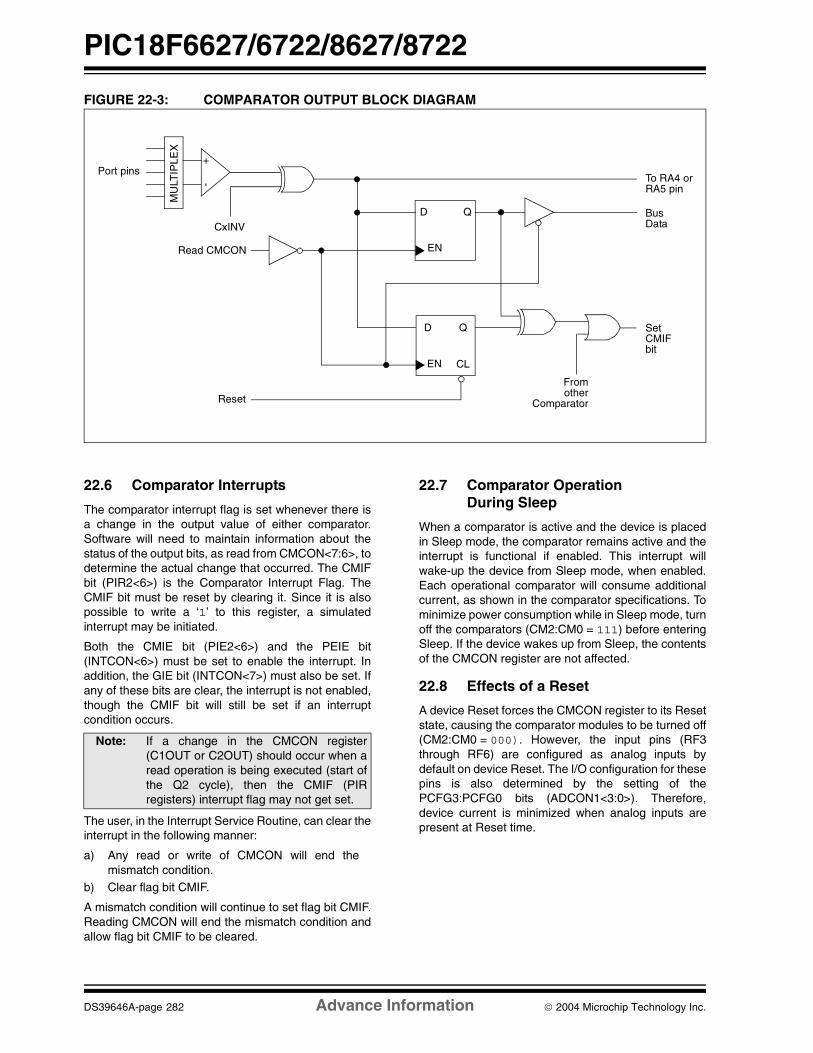
PIC18F6627/6722/8627/8722
DS39646A-page 282 Advance Information 2004 Microchip Technology Inc.
FIGURE 22-3: COMPARATOR OUTPUT BLOCK DIAGRAM
22.6 Comparator Interrupts
The comparator interrupt flag is set whenever there isa change in the output value of either comparator.Software will need to maintain information about thestatus of the output bits, as read from CMCON<7:6>, todetermine the actual change that occurred. The CMIFbit (PIR2<6>) is the Comparator Interrupt Flag. TheCMIF bit must be reset by clearing it. Since it is alsopossible to write a ‘1’ to this register, a simulatedinterrupt may be initiated.
Both the CMIE bit (PIE2<6>) and the PEIE bit(INTCON<6>) must be set to enable the interrupt. Inaddition, the GIE bit (INTCON<7>) must also be set. Ifany of these bits are clear, the interrupt is not enabled,though the CMIF bit will still be set if an interruptcondition occurs.
The user, in the Interrupt Service Routine, can clear theinterrupt in the following manner:
a) Any read or write of CMCON will end themismatch condition.
b) Clear flag bit CMIF.
A mismatch condition will continue to set flag bit CMIF.Reading CMCON will end the mismatch condition andallow flag bit CMIF to be cleared.
22.7 Comparator Operation During Sleep
When a comparator is active and the device is placedin Sleep mode, the comparator remains active and theinterrupt is functional if enabled. This interrupt willwake-up the device from Sleep mode, when enabled.Each operational comparator will consume additionalcurrent, as shown in the comparator specifications. Tominimize power consumption while in Sleep mode, turnoff the comparators (CM2:CM0 = 111) before enteringSleep. If the device wakes up from Sleep, the contentsof the CMCON register are not affected.
22.8 Effects of a Reset
A device Reset forces the CMCON register to its Resetstate, causing the comparator modules to be turned off(CM2:CM0 = 000). However, the input pins (RF3through RF6) are configured as analog inputs bydefault on device Reset. The I/O configuration for thesepins is also determined by the setting of thePCFG3:PCFG0 bits (ADCON1<3:0>). Therefore,device current is minimized when analog inputs arepresent at Reset time.
D Q
EN
To RA4 orRA5 pin
BusData
Set
MU
LTIP
LEX
CMIFbit
-+
Port pins
Read CMCON
Reset
Fromother
Comparator
CxINV
D Q
EN CL
Note: If a change in the CMCON register(C1OUT or C2OUT) should occur when aread operation is being executed (start ofthe Q2 cycle), then the CMIF (PIRregisters) interrupt flag may not get set.

2004 Microchip Technology Inc. Advance Information DS39646A-page 283
PIC18F6627/6722/8627/8722
22.9 Analog Input ConnectionConsiderations
A simplified circuit for an analog input is shown inFigure 22-4. Since the analog pins are connected to adigital output, they have reverse biased diodes to VDD
and VSS. The analog input, therefore, must be betweenVSS and VDD. If the input voltage deviates from this
range by more than 0.6V in either direction, one of thediodes is forward biased and a latch-up condition mayoccur. A maximum source impedance of 10 kΩ isrecommended for the analog sources. Any externalcomponent connected to an analog input pin, such asa capacitor or a Zener diode, should have very littleleakage current.
FIGURE 22-4: COMPARATOR ANALOG INPUT MODEL
TABLE 22-1: REGISTERS ASSOCIATED WITH COMPARATOR MODULE
VA
RS < 10k
AIN
CPIN5 pF
VDD
VT = 0.6V
VT = 0.6V
RIC
ILEAKAGE±500 nA
VSS
Legend: CPIN = Input CapacitanceVT = Threshold VoltageILEAKAGE = Leakage Current at the pin due to various junctionsRIC = Interconnect ResistanceRS = Source ImpedanceVA = Analog Voltage
ComparatorInput
Name Bit 7 Bit 6 Bit 5 Bit 4 Bit 3 Bit 2 Bit 1 Bit 0Reset Values
on page
CMCON C2OUT C1OUT C2INV C1INV CIS CM2 CM1 CM0 59
CVRCON CVREN CVROE CVRR CVRSS CVR3 CVR2 CVR1 CVR0 59
INTCON GIE/GIEH PEIE/GIEL TMR0IE INT0IE RBIE TMR0IF INT0IF RBIF 60
PIR2 OSCFIF CMIF — EEIF BCL1IF HLVDIF TMR3IF CCP2IF 60
PIE2 OSCFIE CMIE — EEIE BCL1IE HLVDIE TMR3IE CCP2IE 60
IPR2 OSCFIP CMIP — EEIP BCL1IP HLVDIP TMR3IP CCP2IP 60
TRISF PORTF Data Direction Control Register 60
Legend: — = unimplemented, read as ‘0’. Shaded cells are unused by the comparator module.

PIC18F6627/6722/8627/8722
DS39646A-page 284 Advance Information 2004 Microchip Technology Inc.
NOTES:

2004 Microchip Technology Inc. Advance Information DS39646A-page 285
PIC18F6627/6722/8627/8722
23.0 COMPARATOR VOLTAGE REFERENCE MODULE
The comparator voltage reference is a 16-tap resistorladder network that provides a selectable referencevoltage. Although its primary purpose is to provide areference for the analog comparators, it may also beused independently of them.
A block diagram of the module is shown in Figure 23-1.The resistor ladder is segmented to provide two rangesof CVREF values and has a power-down function toconserve power when the reference is not being used.The module’s supply reference can be provided fromeither device VDD/VSS or an external voltage reference.
23.1 Configuring the Comparator Voltage Reference
The voltage reference module is controlled through theCVRCON register (Register 23-1). The comparatorvoltage reference provides two ranges of outputvoltage, each with 16 distinct levels. The range to be
used is selected by the CVRR bit (CVRCON<5>). Theprimary difference between the ranges is the size of thesteps selected by the CVREF Selection bits(CVR3:CVR0), with one range offering finer resolution.The equations used to calculate the output of thecomparator voltage reference are as follows:
If CVRR = 1: CVREF = ((CVR3:CVR0)/24) x (CVRSRC)
If CVRR = 0: CVREF = (CVRSRC/4) + ((CVR3:CVR0)/32) x(CVRSRC)
The comparator reference supply voltage can comefrom either VDD and VSS, or the external VREF+ andVREF- that are multiplexed with RA2 and RA3. Thevoltage source is selected by the CVRSS bit(CVRCON<4>).
The settling time of the comparator voltage referencemust be considered when changing the CVREF out-put (see Table 28-3 in Section 28.0 “ElectricalCharacteristics”).
REGISTER 23-1: CVRCON: COMPARATOR VOLTAGE REFERENCE CONTROL REGISTER R/W-0 R/W-0 R/W-0 R/W-0 R/W-0 R/W-0 R/W-0 R/W-0
CVREN CVROE(1) CVRR CVRSS CVR3 CVR2 CVR1 CVR0
bit 7 bit 0
bit 7 CVREN: Comparator Voltage Reference Enable bit1 = CVREF circuit powered on 0 = CVREF circuit powered down
bit 6 CVROE: Comparator VREF Output Enable bit(1)
1 = CVREF voltage level is also output on the RF5/AN10/CVREF pin 0 = CVREF voltage is disconnected from the RF5/AN10/CVREF pin
Note 1: CVROE overrides the TRISF<5> bit setting.
bit 5 CVRR: Comparator VREF Range Selection bit
1 = 0 to 0.667 CVRSRC, with CVRSRC/24 step size (low range)0 = 0.25 CVRSRC to 0.75 CVRSRC, with CVRSRC/32 step size (high range)
bit 4 CVRSS: Comparator VREF Source Selection bit1 = Comparator reference source, CVRSRC = (VREF+) – (VREF-)0 = Comparator reference source, CVRSRC = AVDD – AVSS
bit 3-0 CVR3:CVR0: Comparator VREF Value Selection bits (0 ≤ (CVR3:CVR0) ≤ 15) When CVRR = 1: CVREF = ((CVR3:CVR0)/24) • (CVRSRC)When CVRR = 0: CVREF = (CVRSRC/4) + ((CVR3:CVR0)/32) • (CVRSRC)
Legend:
R = Readable bit W = Writable bit U = Unimplemented bit, read as ‘0’
-n = Value at POR ‘1’ = Bit is set ‘0’ = Bit is cleared x = Bit is unknown
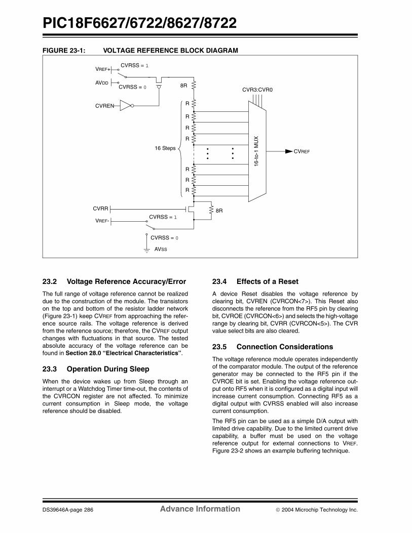
PIC18F6627/6722/8627/8722
DS39646A-page 286 Advance Information 2004 Microchip Technology Inc.
FIGURE 23-1: VOLTAGE REFERENCE BLOCK DIAGRAM
23.2 Voltage Reference Accuracy/Error
The full range of voltage reference cannot be realizeddue to the construction of the module. The transistorson the top and bottom of the resistor ladder network(Figure 23-1) keep CVREF from approaching the refer-ence source rails. The voltage reference is derivedfrom the reference source; therefore, the CVREF outputchanges with fluctuations in that source. The testedabsolute accuracy of the voltage reference can befound in Section 28.0 “Electrical Characteristics”.
23.3 Operation During Sleep
When the device wakes up from Sleep through aninterrupt or a Watchdog Timer time-out, the contents ofthe CVRCON register are not affected. To minimizecurrent consumption in Sleep mode, the voltagereference should be disabled.
23.4 Effects of a Reset
A device Reset disables the voltage reference byclearing bit, CVREN (CVRCON<7>). This Reset alsodisconnects the reference from the RF5 pin by clearingbit, CVROE (CVRCON<6>) and selects the high-voltagerange by clearing bit, CVRR (CVRCON<5>). The CVRvalue select bits are also cleared.
23.5 Connection Considerations
The voltage reference module operates independentlyof the comparator module. The output of the referencegenerator may be connected to the RF5 pin if theCVROE bit is set. Enabling the voltage reference out-put onto RF5 when it is configured as a digital input willincrease current consumption. Connecting RF5 as adigital output with CVRSS enabled will also increasecurrent consumption.
The RF5 pin can be used as a simple D/A output withlimited drive capability. Due to the limited current drivecapability, a buffer must be used on the voltagereference output for external connections to VREF.Figure 23-2 shows an example buffering technique.
16-t
o-1
MU
X
CVR3:CVR08R
RCVREN
CVRSS = 0AVDD
VREF+CVRSS = 1
8R
CVRSS = 0
VREF-CVRSS = 1
R
R
R
R
R
R
16 Steps
CVRR
CVREF
AVSS

2004 Microchip Technology Inc. Advance Information DS39646A-page 287
PIC18F6627/6722/8627/8722
FIGURE 23-2: VOLTAGE REFERENCE OUTPUT BUFFER EXAMPLE
TABLE 23-1: REGISTERS ASSOCIATED WITH COMPARATOR VOLTAGE REFERENCE
CVREF Output+–
CVREF
Module
Voltage Reference
Output Impedance
R(1)
RF5
Note 1: R is dependent upon the voltage reference configuration bits, CVRCON<3:0> and CVRCON<5>.
PIC18FXXXX
Name Bit 7 Bit 6 Bit 5 Bit 4 Bit 3 Bit 2 Bit 1 Bit 0Reset Values
on page
CVRCON CVREN CVROE CVRR CVRSS CVR3 CVR2 CVR1 CVR0 59
CMCON C2OUT C1OUT C2INV C1INV CIS CM2 CM1 CM0 59
TRISF PORTF Data Direction Control Register 60
Legend: Shaded cells are not used with the comparator voltage reference.

PIC18F6627/6722/8627/8722
DS39646A-page 288 Advance Information 2004 Microchip Technology Inc.
NOTES:

2004 Microchip Technology Inc. Advance Information DS39646A-page 289
PIC18F6627/6722/8627/8722
24.0 HIGH/LOW-VOLTAGE DETECT (HLVD)
PIC18F6627/6722/8627/8722 devices have aHigh/Low-Voltage Detect module (HLVD). This is a pro-grammable circuit that allows the user to specify both adevice voltage trip point and the direction of change fromthat point. If the device experiences an excursion pastthe trip point in that direction, an interrupt flag is set. If theinterrupt is enabled, the program execution will branch tothe interrupt vector address and the software can thenrespond to the interrupt.
The High/Low-Voltage Detect Control register(Register 24-1) completely controls the operation of theHLVD module. This allows the circuitry to be “turnedoff” by the user under software control, whichminimizes the current consumption for the device.
The block diagram for the HLVD module is shown inFigure 24-1.
REGISTER 24-1: HLVDCON: HIGH/LOW-VOLTAGE DETECT CONTROL REGISTER R/W-0 U-0 R-0 R/W-0 R/W-0 R/W-1 R/W-0 R/W-1
VDIRMAG — IRVST HLVDEN HLVDL3(1) HLVDL2(1) HLVDL1(1) HLVDL0(1)
bit 7 bit 0
bit 7 VDIRMAG: Voltage Direction Magnitude Select bit1 = Event occurs when voltage equals or exceeds trip point (HLVDL3:HLDVL0)0 = Event occurs when voltage equals or falls below trip point (HLVDL3:HLVDL0)
bit 6 Unimplemented: Read as ‘0’
bit 5 IRVST: Internal Reference Voltage Stable Flag bit
1 = Indicates that the voltage detect logic will generate the interrupt flag at the specified voltagerange
0 = Indicates that the voltage detect logic will not generate the interrupt flag at the specifiedvoltage range and the HLVD interrupt should not be enabled
bit 4 HLVDEN: High/Low-Voltage Detect Power Enable bit
1 = HLVD enabled0 = HLVD disabled
bit 3-0 HLVDL3:HLVDL0: Voltage Detection Limit bits(1)
1111 = External analog input is used (input comes from the HLVDIN pin) 1110 = Maximum setting ...0000 = Minimum setting
Note 1: See Table 28-4 for specifications.
Legend:
R = Readable bit W = Writable bit U = Unimplemented bit, read as ‘0’
-n = Value at POR ‘1’ = Bit is set ‘0’ = Bit is cleared x = Bit is unknown
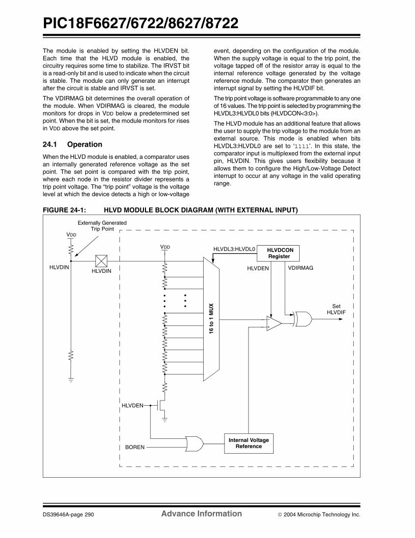
PIC18F6627/6722/8627/8722
DS39646A-page 290 Advance Information 2004 Microchip Technology Inc.
The module is enabled by setting the HLVDEN bit.Each time that the HLVD module is enabled, thecircuitry requires some time to stabilize. The IRVST bitis a read-only bit and is used to indicate when the circuitis stable. The module can only generate an interruptafter the circuit is stable and IRVST is set.
The VDIRMAG bit determines the overall operation ofthe module. When VDIRMAG is cleared, the modulemonitors for drops in VDD below a predetermined setpoint. When the bit is set, the module monitors for risesin VDD above the set point.
24.1 Operation
When the HLVD module is enabled, a comparator usesan internally generated reference voltage as the setpoint. The set point is compared with the trip point,where each node in the resistor divider represents atrip point voltage. The “trip point” voltage is the voltagelevel at which the device detects a high or low-voltage
event, depending on the configuration of the module.When the supply voltage is equal to the trip point, thevoltage tapped off of the resistor array is equal to theinternal reference voltage generated by the voltagereference module. The comparator then generates aninterrupt signal by setting the HLVDIF bit.
The trip point voltage is software programmable to any oneof 16 values. The trip point is selected by programming theHLVDL3:HLVDL0 bits (HLVDCON<3:0>).
The HLVD module has an additional feature that allowsthe user to supply the trip voltage to the module from anexternal source. This mode is enabled when bitsHLVDL3:HLVDL0 are set to ‘1111’. In this state, thecomparator input is multiplexed from the external inputpin, HLVDIN. This gives users flexibility because itallows them to configure the High/Low-Voltage Detectinterrupt to occur at any voltage in the valid operatingrange.
FIGURE 24-1: HLVD MODULE BLOCK DIAGRAM (WITH EXTERNAL INPUT)
Set
VDD
16 t
o 1
MU
X
HLVDEN
HLVDCON
HLVDIN
HLVDL3:HLVDL0Register
HLVDIN
VDD
Externally GeneratedTrip Point
HLVDIF
HLVDEN
BORENInternal Voltage
Reference
VDIRMAG

2004 Microchip Technology Inc. Advance Information DS39646A-page 291
PIC18F6627/6722/8627/8722
24.2 HLVD Setup
The following steps are needed to set up the HLVDmodule:
1. Write the value to the HLVDL3:HLVDL0 bits thatselects the desired HLVD trip point.
2. Set the VDIRMAG bit to detect high voltage(VDIRMAG = 1) or low voltage (VDIRMAG = 0).
3. Enable the HLVD module by setting theHLVDEN bit.
4. Clear the HLVD interrupt flag (PIR2<2>), whichmay have been set from a previous interrupt.
5. Enable the HLVD interrupt if interrupts aredesired by setting the HLVDIE and GIE bits(PIE2<2> and INTCON<7>). An interrupt will notbe generated until the IRVST bit is set.
24.3 Current Consumption
When the module is enabled, the HLVD comparatorand voltage divider are enabled and will consume staticcurrent. The total current consumption, when enabled,is specified in electrical specification parameter D022B(Section 28.2 “DC Characteristics”).
Depending on the application, the HLVD module doesnot need to be operating constantly. To decrease thecurrent requirements, the HLVD circuitry may onlyneed to be enabled for short periods where the voltageis checked. After doing the check, the HLVD modulemay be disabled.
24.4 HLVD Start-up Time
The internal reference voltage of the HLVD module,specified in electrical specification parameter D420(Section 28.2 “DC Characteristics”), may be usedby other internal circuitry, such as the ProgrammableBrown-out Reset. If the HLVD or other circuits using thevoltage reference are disabled to lower the device’scurrent consumption, the reference voltage circuit willrequire time to become stable before a low orhigh-voltage condition can be reliably detected. Thisstart-up time, TIRVST, is an interval that is independentof device clock speed. It is specified in electricalspecification parameter 36 (Table 28-12).
The HLVD interrupt flag is not enabled until TIRVST hasexpired and a stable reference voltage is reached. Forthis reason, brief excursions beyond the set point maynot be detected during this interval. Refer toFigure 24-2 or Figure 24-3.
FIGURE 24-2: LOW-VOLTAGE DETECT OPERATION (VDIRMAG = 0)
VHLVD
VDD
HLVDIF
VHLVD
VDD
Enable HLVD
TIRVST
HLVDIF may not be set
Enable HLVD
HLVDIF
HLVDIF cleared in software
HLVDIF cleared in software
HLVDIF cleared in software,
CASE 1:
CASE 2:
HLVDIF remains set since HLVD condition still exists
TIRVST
Internal Reference is stable
Internal Reference is stable
IRVST
IRVST

PIC18F6627/6722/8627/8722
DS39646A-page 292 Advance Information 2004 Microchip Technology Inc.
FIGURE 24-3: HIGH-VOLTAGE DETECT OPERATION (VDIRMAG = 1)
24.5 Applications
In many applications, the ability to detect a drop belowor rise above a particular threshold is desirable. Forexample, the HLVD module could be periodicallyenabled to detect Universal Serial Bus (USB) attach ordetach. This assumes the device is powered by a lowervoltage source than the USB when detached. An attachwould indicate a high-voltage detect from, for example,3.3V to 5V (the voltage on USB) and vice versa for adetach. This feature could save a design a few extracomponents and an attach signal (input pin).
For general battery applications, Figure 24-4 shows apossible voltage curve. Over time, the device voltagedecreases. When the device voltage reaches voltageVA, the HLVD logic generates an interrupt at time TA.The interrupt could cause the execution of an ISR,which would allow the application to perform “house-keeping tasks” and perform a controlled shutdownbefore the device voltage exits the valid operatingrange at TB. The HLVD, thus, would give the applica-tion a time window, represented by the differencebetween TA and TB, to safely exit.
FIGURE 24-4: TYPICAL LOW-VOLTAGE DETECT APPLICATION
VHLVD
VDD
HLVDIF
VHLVD
VDD
Enable HLVD
TIRVST
HLVDIF may not be set
Enable HLVD
HLVDIF
HLVDIF cleared in software
HLVDIF cleared in software
HLVDIF cleared in software,
CASE 1:
CASE 2:
HLVDIF remains set since HLVD condition still exists
TIRVST
IRVST
Internal Reference is stable
Internal Reference is stable
IRVST
Time
Vo
ltag
e
VA
VB
TA TB
VA = HLVD trip pointVB = Minimum valid device operating voltage
Legend:

2004 Microchip Technology Inc. Advance Information DS39646A-page 293
PIC18F6627/6722/8627/8722
24.6 Operation During Sleep
When enabled, the HLVD circuitry continues to operateduring Sleep. If the device voltage crosses the trippoint, the HLVDIF bit will be set and the device willwake-up from Sleep. Device execution will continuefrom the interrupt vector address if interrupts havebeen globally enabled.
24.7 Effects of a Reset
A device Reset forces all registers to their Reset state.This forces the HLVD module to be turned off.
TABLE 24-1: REGISTERS ASSOCIATED WITH HIGH/LOW-VOLTAGE DETECT MODULE
Name Bit 7 Bit 6 Bit 5 Bit 4 Bit 3 Bit 2 Bit 1 Bit 0Reset Values
on Page
HLVDCON VDIRMAG — IRVST HLVDEN HLVDL3 HLVDL2 HLVDL1 HLVDL0 58
INTCON GIE/GIEH PEIE/GIEL TMR0IE INT0IE RBIE TMR0IF INT0IF RBIF 57
PIR2 OSCFIF CMIF — EEIF BCL1IF HLVDIF TMR3IF CCP2IF 60
PIE2 OSCFIE CMIE — EEIE BCL1IE HLVDIE TMR3IE CCP2IE 60
IPR2 OSCFIP CMIP — EEIP BCL1IP HLVDIP TMR3IP CCP2IP 60
TRISA TRISA7(1) TRISA6(1) PORTA Data Direction Control Register 60
Legend: — = unimplemented, read as ‘0’. Shaded cells are unused by the HLVD module.Note 1: PORTA<7:6> and their direction bits are individually configured as port pins based on various primary
oscillator modes. When disabled, these bits read as ‘0’.

PIC18F6627/6722/8627/8722
DS39646A-page 294 Advance Information 2004 Microchip Technology Inc.
NOTES:

2004 Microchip Technology Inc. Advance Information DS39646A-page 295
PIC18F6627/6722/8627/8722
25.0 SPECIAL FEATURES OF THE CPU
PIC18F6627/6722/8627/8722 devices include severalfeatures intended to maximize reliability and minimizecost through elimination of external components. Theseare:
• Oscillator Selection• Resets:
- Power-on Reset (POR)- Power-up Timer (PWRT)- Oscillator Start-up Timer (OST)- Brown-out Reset (BOR)
• Interrupts• Watchdog Timer (WDT)• Fail-Safe Clock Monitor• Two-Speed Start-up• Code Protection• ID Locations• In-Circuit Serial Programming
The oscillator can be configured for the applicationdepending on frequency, power, accuracy and cost. Allof the options are discussed in detail in Section 2.0“Oscillator Configurations”.
A complete discussion of device Resets and interruptsis available in previous sections of this data sheet.
In addition to their Power-up and Oscillator Start-upTimers provided for Resets, PIC18F6627/6722/8627/8722 devices have a Watchdog Timer, which is eitherpermanently enabled via the configuration bits orsoftware controlled (if configured as disabled).
The inclusion of an internal RC oscillator also providesthe additional benefits of a Fail-Safe Clock Monitor(FSCM) and Two-Speed Start-up. FSCM provides forbackground monitoring of the peripheral clock andautomatic switchover in the event of its failure. Two-Speed Start-up enables code to be executed almostimmediately on start-up, while the primary clock sourcecompletes its start-up delays.
All of these features are enabled and configured bysetting the appropriate configuration register bits.
25.1 Configuration Bits
The configuration bits can be programmed (read as ‘0’)or left unprogrammed (read as ‘1’) to select variousdevice configurations. These bits are mapped startingat program memory location 300000h.
The user will note that address 300000h is beyond theuser program memory space. In fact, it belongs to theconfiguration memory space (300000h-3FFFFFh), whichcan only be accessed using table reads and table writes.
Programming the configuration registers is done in amanner similar to programming the Flash memory. TheWR bit in the EECON1 register starts a self-timed writeto the configuration register. In normal operation mode,a TBLWT instruction with the TBLPTR pointing to theconfiguration register sets up the address and the datafor the configuration register write. Setting the WR bitstarts a long write to the configuration register. Theconfiguration registers are written a byte at a time. Towrite or erase a configuration cell, a TBLWT instructioncan write a ‘1’ or a ‘0’ into the cell. For additional detailson Flash programming, refer to Section 6.5 “Writingto Flash Program Memory”.
TABLE 25-1: CONFIGURATION BITS AND DEVICE IDs
File Name Bit 7 Bit 6 Bit 5 Bit 4 Bit 3 Bit 2 Bit 1 Bit 0Default/
UnprogrammedValue
300001h CONFIG1H IESO FCMEN — — FOSC3 FOSC2 FOSC1 FOSC0 00-- 0111
300002h CONFIG2L — — — BORV1 BORV0 BOREN1 BOREN0 PWRTEN ---1 1111
300003h CONFIG2H — — — WDTPS3 WDTPS2 WDTPS1 WDTPS0 WDTEN ---1 1111
300004h CONFIG3L(3) WAIT BW ABW1 ABW0 — — PM1 PM0 1111 --11
300005h CONFIG3H MCLRE — — — — LPT1OSC ECCPMX(3) CCP2MX 1--- -011
300006h CONFIG4L DEBUG XINST BBSIZ1 BBSIZ0 — LVP — STVREN 1000 -1-1
300008h CONFIG5L CP7(1) CP6(1) CP5 CP4 CP3 CP2 CP1 CP0 1111 1111
300009h CONFIG5H CPD CPB — — — — — — 11-- ----
30000Ah CONFIG6L WRT7(1) WRT6(1) WRT5 WRT4 WRT3 WRT2 WRT1 WRT0 1111 1111
30000Bh CONFIG6H WRTD WRTB WRTC — — — — — 111- ----
30000Ch CONFIG7L EBRT7(1) EBRT6(1) EBTR5 EBTR4 EBTR3 EBTR2 EBTR1 EBTR0 1111 1111
30000Dh CONFIG7H — EBTRB — — — — — — -1-- ----
3FFFFEh DEVID1(2) DEV2 DEV1 DEV0 REV4 REV3 REV2 REV1 REV0 xxxx xxxx
3FFFFFh DEVID2(2) DEV10 DEV9 DEV8 DEV7 DEV6 DEV5 DEV4 DEV3 0000 1100
Legend: x = unknown, u = unchanged, — = unimplemented, q = value depends on condition. Shaded cells are unimplemented, read as ‘0’.
Note 1: Unimplemented in PIC18F6627/8627 devices; maintain this bit set.2: See Register 25-13 for DEVID1 values. DEVID registers are read-only and cannot be programmed by the user.3: Unimplemented in PIC18F6627/6722 devices.

PIC18F6627/6722/8627/8722
DS39646A-page 296 Advance Information 2004 Microchip Technology Inc.
REGISTER 25-1: CONFIG1H: CONFIGURATION REGISTER 1 HIGH (BYTE ADDRESS 300001h) R/P-0 R/P-0 U-0 U-0 R/P-0 R/P-1 R/P-1 R/P-1
IESO FCMEN — — FOSC3 FOSC2 FOSC1 FOSC0
bit 7 bit 0
bit 7 IESO: Internal/External Oscillator Switchover bit
1 = Two-Speed Start-up enabled0 = Two-Speed Start-up disabled
bit 6 FCMEN: Fail-Safe Clock Monitor Enable bit1 = Fail-Safe Clock Monitor enabled0 = Fail-Safe Clock Monitor disabled
bit 5-4 Unimplemented: Read as ‘0’
bit 3-0 FOSC3:FOSC0: Oscillator Selection bits
11xx = External RC oscillator, CLKO function on RA6101x = External RC oscillator, CLKO function on RA61001 = Internal oscillator block, CLKO function on RA6, port function on RA71000 = Internal oscillator block, port function on RA6 and RA70111 = External RC oscillator, port function on RA60110 = HS oscillator, PLL enabled (Clock Frequency = 4 x FOSC1)0101 = EC oscillator, port function on RA60100 = EC oscillator, CLKO function on RA60011 = External RC oscillator, CLKO function on RA60010 = HS oscillator0001 = XT oscillator0000 = LP oscillator
Legend:
R = Readable bit P = Programmable bit U = Unimplemented bit, read as ‘0’
-n = Value when device is unprogrammed u = Unchanged from programmed state

2004 Microchip Technology Inc. Advance Information DS39646A-page 297
PIC18F6627/6722/8627/8722
REGISTER 25-2: CONFIG2L: CONFIGURATION REGISTER 2 LOW (BYTE ADDRESS 300002h) U-0 U-0 U-0 R/P-1 R/P-1 R/P-1 R/P-1 R/P-1
— — — BORV1(1) BORV0(1) BOREN1(2) BOREN0(2) PWRTEN(2)
bit 7 bit 0
bit 7-5 Unimplemented: Read as ‘0’
bit 4-3 BORV1:BORV0: Brown-out Reset Voltage bits(1)
11 = Maximum setting ...00 = Minimum setting
bit 2-1 BOREN1:BOREN0: Brown-out Reset Enable bits(2)
11 = Brown-out Reset enabled in hardware only (SBOREN is disabled)10 = Brown-out Reset enabled in hardware only and disabled in Sleep mode
(SBOREN is disabled) 01 = Brown-out Reset enabled and controlled by software (SBOREN is enabled) 00 = Brown-out Reset disabled in hardware and software
bit 0 PWRTEN: Power-up Timer Enable bit(2)
1 = PWRT disabled 0 = PWRT enabled
Note 1: See Section 28.1 “DC Characteristics: Supply Voltage” for specifications.
2: The Power-up Timer is decoupled from Brown-out Reset, allowing these features tobe independently controlled.
Legend:
R = Readable bit P = Programmable bit U = Unimplemented bit, read as ‘0’
-n = Value when device is unprogrammed u = Unchanged from programmed state

PIC18F6627/6722/8627/8722
DS39646A-page 298 Advance Information 2004 Microchip Technology Inc.
REGISTER 25-3: CONFIG2H: CONFIGURATION REGISTER 2 HIGH (BYTE ADDRESS 300003h) U-0 U-0 U-0 R/P-1 R/P-1 R/P-1 R/P-1 R/P-1
— — — WDTPS3 WDTPS2 WDTPS1 WDTPS0 WDTEN
bit 7 bit 0
bit 7-5 Unimplemented: Read as ‘0’
bit 4-1 WDTPS3:WDTPS0: Watchdog Timer Postscale Select bits
1111 = 1:32,7681110 = 1:16,3841101 = 1:8,1921100 = 1:4,0961011 = 1:2,0481010 = 1:1,0241001 = 1:5121000 = 1:2560111 = 1:1280110 = 1:640101 = 1:320100 = 1:160011 = 1:80010 = 1:40001 = 1:20000 = 1:1
bit 0 WDTEN: Watchdog Timer Enable bit
1 = WDT enabled0 = WDT disabled (control is placed on the SWDTEN bit)
Legend:R = Readable bit P = Programmable bit U = Unimplemented bit, read as ‘0’-n = Value when device is unprogrammed u = Unchanged from programmed state

2004 Microchip Technology Inc. Advance Information DS39646A-page 299
PIC18F6627/6722/8627/8722
REGISTER 25-4: CONFIG3L: CONFIGURATION REGISTER 3 LOW (BYTE ADDRESS 300004h)(1) R/P-1 R/P-1 R/P-1 R/P-1 U-0 U-0 R/P-1 R/P-1
WAIT BW ABW1 ABW0 — — PM1 PM0
bit 7 bit 0
bit 7 WAIT: External Bus Wait Enable bit1 = Wait selections from MEMCON.WAIT<1:0> unavailable, and the device will not wait0 = Wait programmed by MEMCON.WAIT<1:0>
bit 6 BW: Data Bus Width Select bit
1 = 16-bit External Bus mode0 = 8-bit External Bus mode
bit 5-4 ABW<1:0>: Address Bus Width Select bits11 = 20-bit Address bus10 = 16-bit Address bus01 = 12-bit Address bus00 = 8-bit Address bus
bit 3-2 Unimplemented: Read as ‘0’
bit 1-0 PM<1:0>: Processor Data Memory Mode Select bits11 = Microcontroller mode10 = Microprocessor mode01 = Microprocessor with Boot Block mode00 = Extended Microcontroller mode
Note 1: This register is unimplemented in PIC18F6627/6722 devices; maintain these bitsset.
Legend:R = Readable bit P = Programmable bit U = Unimplemented bit, read as ‘0’-n = Value when device is unprogrammed u = Unchanged from programmed state

PIC18F6627/6722/8627/8722
DS39646A-page 300 Advance Information 2004 Microchip Technology Inc.
REGISTER 25-5: CONFIG3H: CONFIGURATION REGISTER 3 HIGH (BYTE ADDRESS 300005h) R/P-1 U-0 U-0 U-0 U-0 R/P-0 R/P-1 R/P-1
MCLRE — — — — LPT1OSC ECCPMX(1) CCP2MX
bit 7 bit 0
bit 7 MCLRE: MCLR Pin Enable bit 1 = MCLR pin enabled; RE3 input pin disabled0 = RE3 input pin enabled; MCLR disabled
bit 6-3 Unimplemented: Read as ‘0’
bit 2 LPT1OSC: Low-Power Timer1 Oscillator Enable bit1 = Timer1 configured for low-power operation0 = Timer1 configured for higher power operation
bit 1 ECCPMX: ECCP Mux bit(1)
1 = Enhanced CCP1/3 (P1B/P1C/P3B/P3C) are multiplexed onto RE6, RE5, RE4 and RE3respectively
0 = Enhanced CCP1/3 (P1B/P1C/P3B/P3C) are multiplexed onto RH7, RH6, RH5 and RH4respectively
bit 0 CCP2MX: CCP2 Mux bit1 = ECCP2 input/output is multiplexed with RC1 0 = ECCP2 input/output is multiplexed with RB3 in Extended Microcontroller, Microprocessor or
Microprocessor with Boot Block mode. ECCP2 is multiplexed with RE7 in Microcontrollermode.
Note 1: This feature is only available on PIC18F8627/8722 devices.
Legend:
R = Readable bit P = Programmable bit U = Unimplemented bit, read as ‘0’
-n = Value when device is unprogrammed u = Unchanged from programmed state

2004 Microchip Technology Inc. Advance Information DS39646A-page 301
PIC18F6627/6722/8627/8722
REGISTER 25-6: CONFIG4L: CONFIGURATION REGISTER 4 LOW (BYTE ADDRESS 300006h) R/P-1 R/P-0 R/P-0 R/P-0 U-0 R/P-1 U-0 R/P-1
DEBUG XINST BBSIZ1 BBSIZ0 — LVP — STVREN
bit 7 bit 0
bit 7 DEBUG: Background Debugger Enable bit1 = Background debugger disabled, RB6 and RB7 configured as general purpose I/O pins 0 = Background debugger enabled, RB6 and RB7 are dedicated to In-Circuit Debug
bit 6 XINST: Extended Instruction Set Enable bit1 = Instruction set extension and Indexed Addressing mode enabled 0 = Instruction set extension and Indexed Addressing mode disabled (Legacy mode)
bit 5-4 BBSIZ<1:0>: Boot Block Size Select bits
11 = 4 K words (8 Kbytes) Boot Block size10 = 4 K words (8 Kbytes) Boot Block size01 = 2 K words (4 Kbytes) Boot Block size00 = 1 K word (2 Kbytes) Boot Block size
bit 3 Unimplemented: Read as ‘0’
bit 2 LVP: Single-Supply ICSP™ Enable bit1 = Single-Supply ICSP enabled 0 = Single-Supply ICSP disabled
bit 1 Unimplemented: Read as ‘0’
bit 0 STVREN: Stack Full/Underflow Reset Enable bit
1 = Stack full/underflow will cause Reset 0 = Stack full/underflow will not cause Reset
Legend:
R = Readable bit C = Clearable bit U = Unimplemented bit, read as ‘0’
-n = Value when device is unprogrammed u = Unchanged from programmed state

PIC18F6627/6722/8627/8722
DS39646A-page 302 Advance Information 2004 Microchip Technology Inc.
REGISTER 25-7: CONFIG5L: CONFIGURATION REGISTER 5 LOW (BYTE ADDRESS 300008h) R/C-1 R/C-1 R/C-1 R/C-1 R/C-1 R/C-1 R/C-1 R/C-1
CP7(1) CP6(1) CP5 CP5 CP3 CP2 CP1 CP0
bit 7 bit 0
bit 7 CP7: Code Protection bit(1)
1 = Block 7 (01C000-01FFFFh) not code-protected 0 = Block 7 (01C000-01FFFFh) code-protected
bit 6 CP6: Code Protection bit(1)
1 = Block 6 (01BFFF-018000h) not code-protected 0 = Block 6 (01BFFF-018000h) code-protected
bit 5 CP5: Code Protection bit1 = Block 5 (014000-017FFFh) not code-protected 0 = Block 5 (014000-017FFFh) code-protected
bit 4 CP4: Code Protection bit1 = Block 4 (010000-013FFFh) not code-protected 0 = Block 4 (010000-013FFFh) code-protected
bit 3 CP3: Code Protection bit
1 = Block 3 (00C000-00FFFFh) not code-protected 0 = Block 3 (00C000-00FFFFh) code-protected
bit 2 CP2: Code Protection bit1 = Block 2 (008000-00BFFFh) not code-protected 0 = Block 2 (008000-00BFFFh) code-protected
bit 1 CP1: Code Protection bit1 = Block 1 (004000-007FFFh) not code-protected 0 = Block 1 (004000-007FFFh) code-protected
bit 0 CP0: Code Protection bit
1 = Block 0 (000800-003FFFh) not code-protected 0 = Block 0 (000800-003FFFh) code-protected
Note 1: Unimplemented in PIC18F6627/8627 devices; maintain this bit set.
Legend:
R = Readable bit C = Clearable bit U = Unimplemented bit, read as ‘0’
-n = Value when device is unprogrammed u = Unchanged from programmed state

2004 Microchip Technology Inc. Advance Information DS39646A-page 303
PIC18F6627/6722/8627/8722
REGISTER 25-8: CONFIG5H: CONFIGURATION REGISTER 5 HIGH (BYTE ADDRESS 300009h) R/C-1 R/C-1 U-0 U-0 U-0 U-0 U-0 U-0
CPD CPB — — — — — —
bit 7 bit 0
bit 7 CPD: Data EEPROM Code Protection bit1 = Data EEPROM not code-protected0 = Data EEPROM code-protected
bit 6 CPB: Boot Block Code Protection bit
1 = Boot block (000000-0007FFh) not code-protected0 = Boot block (000000-0007FFh) code-protected
bit 5-0 Unimplemented: Read as ‘0’
Legend:
R = Readable bit C = Clearable bit U = Unimplemented bit, read as ‘0’
-n = Value when device is unprogrammed u = Unchanged from programmed state

PIC18F6627/6722/8627/8722
DS39646A-page 304 Advance Information 2004 Microchip Technology Inc.
REGISTER 25-9: CONFIG6L: CONFIGURATION REGISTER 6 LOW (BYTE ADDRESS 30000Ah)
U-0 U-0 U-0 U-0 R/C-1 R/C-1 R/C-1 R/C-1
WRT7 WRT6 WRT5 WRT4 WRT3 WRT2 WRT1 WRT0
bit 7 bit 0
bit 7 WRT7: Write Protection bit(1)
1 = Block 7 (01C000-01FFFFh) not write-protected 0 = Block 7 (01C000-01FFFFh) write-protected
bit 6 WRT6: Write Protection bit(1)
1 = Block 6 (01BFFF-018000h) not write-protected 0 = Block 6 (01BFFF-018000h) write-protected
bit 5 WRT5: Write Protection bit1 = Block 5 (014000-017FFFh) not write-protected 0 = Block 5 (014000-017FFFh) write-protected
bit 4 WRT4: Write Protection bit1 = Block 4 (010000-013FFFh) not write-protected 0 = Block 4 (010000-013FFFh) write-protected
bit 3 WRT3: Write Protection bit
1 = Block 3 (00C000-00FFFFh) not write-protected 0 = Block 3 (00C000-00FFFFh) write-protected
bit 2 WRT2: Write Protection bit1 = Block 2 (008000-00BFFFh) not write-protected 0 = Block 2 (008000-00BFFFh) write-protected
bit 1 WRT1: Write Protection bit1 = Block 1 (004000-007FFFh) not write-protected 0 = Block 1 (004000-007FFFh) write-protected
bit 0 WRT0: Write Protection bit
1 = Block 0 (000800-003FFFh) not write-protected 0 = Block 0 (000800-003FFFh) write-protected
Note 1: Unimplemented in PIC18F6627/8627 devices; maintain this bit set.
Legend:
R = Readable bit C = Clearable bit U = Unimplemented bit, read as ‘0’
-n = Value when device is unprogrammed u = Unchanged from programmed state

2004 Microchip Technology Inc. Advance Information DS39646A-page 305
PIC18F6627/6722/8627/8722
REGISTER 25-10: CONFIG6H: CONFIGURATION REGISTER 6 HIGH (BYTE ADDRESS 30000Bh) R/C-1 R/C-1 R-1 U-0 U-0 U-0 U-0 U-0
WRTD WRTB WRTC(1) — — — — —
bit 7 bit 0
bit 7 WRTD: Data EEPROM Write Protection bit1 = Data EEPROM not write-protected0 = Data EEPROM write-protected
bit 6 WRTB: Boot Block Write Protection bit
1 = Boot block (000000-0007FFh) not write-protected0 = Boot block (000000-0007FFh) write-protected
bit 5 WRTC: Configuration Register Write Protection bit(1)
1 = Configuration registers (300000-3000FFh) not write-protected0 = Configuration registers (300000-3000FFh) write-protected
Note 1: This bit is read-only in normal Execution mode; it can be written only in Program mode.
bit 4-0 Unimplemented: Read as ‘0’
Legend:
R = Readable bit C = Clearable bit U = Unimplemented bit, read as ‘0’
-n = Value when device is unprogrammed u = Unchanged from programmed state
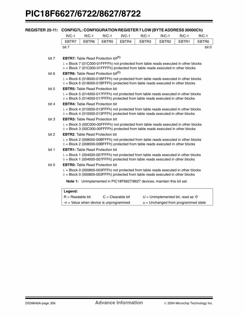
PIC18F6627/6722/8627/8722
DS39646A-page 306 Advance Information 2004 Microchip Technology Inc.
REGISTER 25-11: CONFIG7L: CONFIGURATION REGISTER 7 LOW (BYTE ADDRESS 30000Ch) R/C-1 R/C-1 R/C-1 R/C-1 R/C-1 R/C-1 R/C-1 R/C-1
EBTR7 EBTR6 EBTR5 EBTR4 EBTR3 EBTR2 EBTR1 EBTR0
bit 7 bit 0
bit 7 EBTR7: Table Read Protection bit(1)
1 = Block 7 (01C000-01FFFFh) not protected from table reads executed in other blocks0 = Block 7 (01C000-01FFFFh) protected from table reads executed in other blocks
bit 6 EBTR6: Table Read Protection bit(1)
1 = Block 6 (018000-01BFFFh) not protected from table reads executed in other blocks0 = Block 6 (018000-01BFFFh) protected from table reads executed in other blocks
bit 5 EBTR5: Table Read Protection bit1 = Block 5 (014000-017FFFh) not protected from table reads executed in other blocks0 = Block 5 (014000-017FFFh) protected from table reads executed in other blocks
bit 4 EBTR4: Table Read Protection bit1 = Block 4 (010000-013FFFh) not protected from table reads executed in other blocks0 = Block 4 (010000-013FFFh) protected from table reads executed in other blocks
bit 3 EBTR3: Table Read Protection bit
1 = Block 3 (00C000-00FFFFh) not protected from table reads executed in other blocks0 = Block 3 (00C000-00FFFFh) protected from table reads executed in other blocks
bit 2 EBTR2: Table Read Protection bit1 = Block 2 (008000-00BFFFh) not protected from table reads executed in other blocks 0 = Block 2 (008000-00BFFFh) protected from table reads executed in other blocks
bit 1 EBTR1: Table Read Protection bit1 = Block 1 (004000-007FFFh) not protected from table reads executed in other blocks 0 = Block 1 (004000-007FFFh) protected from table reads executed in other blocks
bit 0 EBTR0: Table Read Protection bit
1 = Block 0 (000800-003FFFh) not protected from table reads executed in other blocks 0 = Block 0 (000800-003FFFh) protected from table reads executed in other blocks
Note 1: Unimplemented in PIC18F6627/8627 devices; maintain this bit set.
Legend:
R = Readable bit C = Clearable bit U = Unimplemented bit, read as ‘0’
-n = Value when device is unprogrammed u = Unchanged from programmed state

2004 Microchip Technology Inc. Advance Information DS39646A-page 307
PIC18F6627/6722/8627/8722
REGISTER 25-12: CONFIG7H: CONFIGURATION REGISTER 7 HIGH (BYTE ADDRESS 30000Dh)
REGISTER 25-13: DEVID1: DEVICE ID REGISTER 1 FOR PIC18F6627/6722/8627/8722
REGISTER 25-14: DEVID2: DEVICE ID REGISTER 2 FOR PIC18F6627/6722/8627/8722
U-0 R/C-1 U-0 U-0 U-0 U-0 U-0 U-0
— EBTRB — — — — — —
bit 7 bit 0
bit 7 Unimplemented: Read as ‘0’
bit 6 EBTRB: Boot Block Table Read Protection bit
1 = Boot block (000000-0007FFh) not protected from table reads executed in other blocks0 = Boot block (000000-0007FFh) protected from table reads executed in other blocks
bit 5-0 Unimplemented: Read as ‘0’
Legend:
R = Readable bit C = Clearable bit U = Unimplemented bit, read as ‘0’
-n = Value when device is unprogrammed u = Unchanged from programmed state
R R R R R R R R
DEV2 DEV1 DEV0 REV4 REV3 REV2 REV1 REV0
bit 7 bit 0
bit 7-5 DEV2:DEV0: Device ID bits001 = PIC18F8722111 = PIC18F8627000 = PIC18F6722110 = PIC18F6627
bit 4-0 REV4:REV0: Revision ID bitsThese bits are used to indicate the device revision.
Legend:
R = Read-only bit P = Programmable bit U = Unimplemented bit, read as ‘0’
-n = Value when device is unprogrammed u = Unchanged from programmed state
R R R R R R R R
DEV10 DEV9 DEV8 DEV7 DEV6 DEV5 DEV4 DEV3
bit 7 bit 0
bit 7-0 DEV10:DEV3: Device ID bits
These bits are used with the DEV2:DEV0 bits in the Device ID Register 1 to identify the part number.
0001 0100 = PIC18F6722/8722 devices0001 0011 = PIC18F6627/8627 devices
Note: These values for DEV10:DEV3 may be shared with other devices. The specificdevice is always identified by using the entire DEV10:DEV0 bit sequence.
Legend:
R = Read-only bit P = Programmable bit U = Unimplemented bit, read as ‘0’
-n = Value when device is unprogrammed u = Unchanged from programmed state

PIC18F6627/6722/8627/8722
DS39646A-page 308 Advance Information 2004 Microchip Technology Inc.
25.2 Watchdog Timer (WDT)
For PIC18F6627/6722/8627/8722 devices, the WDT isdriven by the INTRC source. When the WDT isenabled, the clock source is also enabled. The nominalWDT period is 4 ms and has the same stability as theINTRC oscillator.
The 4 ms period of the WDT is multiplied by a 16-bitpostscaler. Any output of the WDT postscaler isselected by a multiplexer, controlled by bits inConfiguration Register 2H. Available periods rangefrom 4 ms to 131.072 seconds (2.18 minutes). TheWDT and postscaler are cleared when any of thefollowing events occur: a SLEEP or CLRWDT instructionis executed, the IRCF bits (OSCCON<6:4>) arechanged or a clock failure has occurred.
25.2.1 CONTROL REGISTER
Register 25-15 shows the WDTCON register. This is areadable and writable register which contains a controlbit that allows software to override the WDT enableconfiguration bit, but only if the configuration bit hasdisabled the WDT.
FIGURE 25-1: WDT BLOCK DIAGRAM
Note 1: The CLRWDT and SLEEP instructionsclear the WDT and postscaler countswhen executed.
2: Changing the setting of the IRCF bits(OSCCON<6:4>) clears the WDT andpostscaler counts.
3: When a CLRWDT instruction is executed,the postscaler count will be cleared.
INTRC Source
WDT
Wake-up
Reset
WDT Counter
Programmable Postscaler1:1 to 1:32,768
Enable WDT
WDTPS<3:0>
SWDTENWDTEN
CLRWDT
4
from Power
Reset
All Device Resets
Sleep
÷128
Change on IRCF bitsManaged Modes

2004 Microchip Technology Inc. Advance Information DS39646A-page 309
PIC18F6627/6722/8627/8722
REGISTER 25-15: WDTCON: WATCHDOG TIMER CONTROL REGISTER
TABLE 25-2: SUMMARY OF WATCHDOG TIMER REGISTERS
U-0 U-0 U-0 U-0 U-0 U-0 U-0 R/W-0
— — — — — — — SWDTEN(1)
bit 7 bit 0
bit 7-1 Unimplemented: Read as ‘0’
bit 0 SWDTEN: Software Controlled Watchdog Timer Enable bit(1)
1 = Watchdog Timer is on0 = Watchdog Timer is off
Note 1: This bit has no effect if the configuration bit, WDTEN, is enabled.
Legend:
R = Readable bit W = Writable bit
U = Unimplemented bit, read as ‘0’ -n = Value at POR
Name Bit 7 Bit 6 Bit 5 Bit 4 Bit 3 Bit 2 Bit 1 Bit 0Reset Values
on page
RCON IPEN SBOREN — RI TO PD POR BOR 56
WDTCON — — — — — — — SWDTEN 58
Legend: — = unimplemented, read as ‘0’. Shaded cells are not used by the Watchdog Timer.

PIC18F6627/6722/8627/8722
DS39646A-page 310 Advance Information 2004 Microchip Technology Inc.
25.3 Two-Speed Start-up
The Two-Speed Start-up feature helps to minimize thelatency period from oscillator start-up to code executionby allowing the microcontroller to use the INTOSCoscillator as a clock source until the primary clocksource is available. It is enabled by setting the IESOconfiguration bit.
Two-Speed Start-up should be enabled only if theprimary oscillator mode is LP, XT, HS or HSPLL(crystal-based modes). Other sources do not requirean OST start-up delay; for these, Two-Speed Start-upshould be disabled.
When enabled, Resets and wake-ups from Sleep modecause the device to configure itself to run from theinternal oscillator block as the clock source, followingthe time-out of the Power-up Timer after a Power-onReset is enabled. This allows almost immediate codeexecution while the primary oscillator starts and theOST is running. Once the OST times out, the deviceautomatically switches to PRI_RUN mode.
To use a higher clock speed on wake-up, the INTOSCor postscaler clock sources can be selected to providea higher clock speed by setting bits IRCF2:IRCF0immediately after Reset. For wake-ups from Sleep, theINTOSC or postscaler clock sources can be selectedby setting the IRCF2:IRCF0 bits prior to entering Sleepmode.
In all other power-managed modes, Two-Speed Start-up is not used. The device will be clocked by thecurrently selected clock source until the primary clocksource becomes available. The setting of the IESO bitis ignored.
25.3.1 SPECIAL CONSIDERATIONS FOR USING TWO-SPEED START-UP
While using the INTOSC oscillator in Two-Speed Start-up, the device still obeys the normal commandsequences for entering power-managed modes,including multiple SLEEP instructions (refer toSection 3.1.4 “Multiple Sleep Commands”). Inpractice, this means that user code can change theSCS1:SCS0 bit settings or issue SLEEP instructionsbefore the OST times out. This would allow anapplication to briefly wake-up, perform routine“housekeeping” tasks and return to Sleep before thedevice starts to operate from the primary oscillator.
User code can also check if the primary clock source iscurrently providing the device clocking by checking thestatus of the OSTS bit (OSCCON<3>). If the bit is set,the primary oscillator is providing the clock. Otherwise,the internal oscillator block is providing the clock duringwake-up from Reset or Sleep mode.
FIGURE 25-2: TIMING TRANSITION FOR TWO-SPEED START-UP (INTOSC TO HSPLL)
Q1 Q3 Q4
OSC1
Peripheral
ProgramPC PC + 2
INTOSC
PLL Clock
Q1
PC + 6
Q2
Output
Q3 Q4 Q1
CPU Clock
PC + 4
Clock
Counter
Q2 Q2 Q3
Note 1: TOST = 1024 TOSC; TPLL = 2 ms (approx). These intervals are not shown to scale.
2: Clock transition typically occurs within 2-4 TOSC.
Wake from Interrupt Event
TPLL(1)
1 2 n-1 n
Clock
OSTS bit Set
Transition(2)
Multiplexer
TOST(1)

2004 Microchip Technology Inc. Advance Information DS39646A-page 311
PIC18F6627/6722/8627/8722
25.4 Fail-Safe Clock Monitor
The Fail-Safe Clock Monitor (FSCM) allows themicrocontroller to continue operation in the event of anexternal oscillator failure by automatically switching thedevice clock to the internal oscillator block. The FSCMfunction is enabled by setting the FCMEN configurationbit.
When FSCM is enabled, the INTRC oscillator runs atall times to monitor clocks to peripherals and provide abackup clock in the event of a clock failure. Clockmonitoring (shown in Figure 25-3) is accomplished bycreating a sample clock signal, which is the INTRC out-put divided by 64. This allows ample time betweenFSCM sample clocks for a peripheral clock edge tooccur. The peripheral device clock and the sampleclock are presented as inputs to the Clock Monitor latch(CM). The CM is set on the falling edge of the deviceclock source, but cleared on the rising edge of thesample clock.
FIGURE 25-3: FSCM BLOCK DIAGRAM
Clock failure is tested for on the falling edge of the sam-ple clock. If a sample clock falling edge occurs whileCM is still set, a clock failure has been detected(Figure 25-4). This causes the following:
• the FSCM generates an oscillator fail interrupt by setting bit, OSCFIF (PIR2<7>);
• the device clock source is switched to the internal oscillator block (OSCCON is not updated to show the current clock source – this is the fail-safe condition) and
• the WDT is reset.
During switchover, the postscaler frequency from theinternal oscillator block may not be sufficiently stable fortiming sensitive applications. In these cases, it may bedesirable to select another clock configuration and enteran alternate power-managed mode. This can be done toattempt a partial recovery or execute a controlled shut-down. See Section 3.1.4 “Multiple Sleep Commands”and Section 25.3.1 “Special Considerations forUsing Two-Speed Start-up” for more details.
To use a higher clock speed on wake-up, the INTOSC orpostscaler clock sources can be selected to provide ahigher clock speed by setting bits, IRCF2:IRCF0, immedi-ately after Reset. For wake-ups from Sleep, the INTOSCor postscaler clock sources can be selected by setting theIRCF2:IRCF0 bits prior to entering Sleep mode.
The FSCM will detect failures of the primary or second-ary clock sources only. If the internal oscillator blockfails, no failure would be detected, nor would any actionbe possible.
25.4.1 FSCM AND THE WATCHDOG TIMER
Both the FSCM and the WDT are clocked by theINTRC oscillator. Since the WDT operates with aseparate divider and counter, disabling the WDT hasno effect on the operation of the INTRC oscillator whenthe FSCM is enabled.
As already noted, the clock source is switched to theINTOSC clock when a clock failure is detected.Depending on the frequency selected by theIRCF2:IRCF0 bits, this may mean a substantial changein the speed of code execution. If the WDT is enabledwith a small prescale value, a decrease in clock speedallows a WDT time-out to occur and a subsequentdevice Reset. For this reason, fail-safe clock eventsalso reset the WDT and postscaler, allowing it to starttiming from when execution speed was changed anddecreasing the likelihood of an erroneous time-out.
25.4.2 EXITING FAIL-SAFE OPERATION
The fail-safe condition is terminated by either a deviceReset or by entering a power-managed mode. OnReset, the controller starts the primary clock sourcespecified in Configuration Register 1H (with anyrequired start-up delays that are required for theoscillator mode, such as OST or PLL timer). TheINTOSC multiplexer provides the device clock until theprimary clock source becomes ready (similar to a Two-Speed Start-up). The clock source is then switched tothe primary clock (indicated by the OSTS bit in theOSCCON register becoming set). The Fail-Safe ClockMonitor then resumes monitoring the peripheral clock.
The primary clock source may never become readyduring start-up. In this case, operation is clocked by theINTOSC multiplexer. The OSCCON register will remainin its Reset state until a power-managed mode isentered.
Peripheral
INTRC÷ 64
S
C
Q
(32 µs) 488 Hz(2.048 ms)
Clock MonitorLatch (CM)
(edge-triggered)
ClockFailure
Detected
Source
Clock
Q

PIC18F6627/6722/8627/8722
DS39646A-page 312 Advance Information 2004 Microchip Technology Inc.
FIGURE 25-4: FSCM TIMING DIAGRAM
25.4.3 FSCM INTERRUPTS IN POWER-MANAGED MODES
By entering a power-managed mode, the clockmultiplexer selects the clock source selected by theOSCCON register. Fail-Safe Monitoring of the power-managed clock source resumes in the power-managedmode.
If an oscillator failure occurs during power-managedoperation, the subsequent events depend on whetheror not the oscillator failure interrupt is enabled. Ifenabled (OSCFIF = 1), code execution will be clockedby the INTOSC multiplexer. An automatic transitionback to the failed clock source will not occur.
If the interrupt is disabled, subsequent interrupts whilein Idle mode will cause the CPU to begin executinginstructions while being clocked by the INTOSCsource.
25.4.4 POR OR WAKE FROM SLEEP
The FSCM is designed to detect oscillator failure at anypoint after the device has exited Power-on Reset(POR) or low-power Sleep mode. When the primarydevice clock is EC, RC or INTRC modes, monitoringcan begin immediately following these events.
For oscillator modes involving a crystal or resonator(HS, HSPLL, LP or XT), the situation is somewhatdifferent. Since the oscillator may require a start-uptime considerably longer than the FCSM sample clocktime, a false clock failure may be detected. To preventthis, the internal oscillator block is automatically config-ured as the device clock and functions until the primaryclock is stable (the OST and PLL timers have timedout). This is identical to Two-Speed Start-up mode.Once the primary clock is stable, the INTRC returns toits role as the FSCM source.
As noted in Section 25.3.1 “Special Considerationsfor Using Two-Speed Start-up”, it is also possible toselect another clock configuration and enter analternate power-managed mode while waiting for theprimary clock to become stable. When the new power-managed mode is selected, the primary clock isdisabled.
OSCFIF
CM Output
DeviceClock
Output
Sample Clock
FailureDetected
OscillatorFailure
Note: The device clock is normally at a much higher frequency than the sample clock. The relative frequencies in thisexample have been chosen for clarity.
(Q)
CM Test CM Test CM Test
Note: The same logic that prevents false oscilla-tor failure interrupts on POR, or wake fromSleep, will also prevent the detection ofthe oscillator’s failure to start at all follow-ing these events. This can be avoided bymonitoring the OSTS bit and using atiming routine to determine if the oscillatoris taking too long to start. Even so, nooscillator failure interrupt will be flagged.
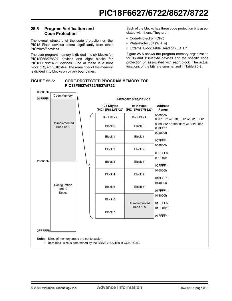
2004 Microchip Technology Inc. Advance Information DS39646A-page 313
PIC18F6627/6722/8627/8722
25.5 Program Verification and Code Protection
The overall structure of the code protection on thePIC18 Flash devices differs significantly from otherPICmicro® devices.
The user program memory is divided into six blocks forPIC18F6627/8627 devices and eight blocks forPIC18F6722/8722 devices. One of these is a bootblock of 2, 4 or 8 Kbytes. The remainder of the memoryis divided into blocks on binary boundaries.
Each of the blocks has three code protection bits asso-ciated with them. They are:
• Code-Protect bit (CPn)• Write-Protect bit (WRTn)• External Block Table Read bit (EBTRn)
Figure 25-5 shows the program memory organizationfor 96 and 128-Kbyte devices and the specific codeprotection bit associated with each block. The actuallocations of the bits are summarized in Table 25-3.
FIGURE 25-5: CODE-PROTECTED PROGRAM MEMORY FOR PIC18F6627/6722/8627/8722
000000h
200000h
3FFFFFh
01FFFFh
Note: Sizes of memory areas are not to scale.* Boot Block size is determined by the BBSIZ<1:0> bits in CONFIG4L.
Code Memory
UnimplementedRead as ‘0’
Configurationand IDSpace
MEMORY SIZE/DEVICE
128 Kbytes(PIC18F6722/8722)
96 Kbytes(PIC18F6627/8627)
Address Range
Boot Block Boot Block000000h0007FFh* or 000FFFh* or 001FFFh*
Block 0 Block 0000800h* or 001000h* or 002000h*003FFFh
Block 1 Block 1004000h
007FFFh
Block 2 Block 2008000h
00BFFFh
Block 3 Block 300C000h
00FFFFh
Block 4 Block 2010000h
013FFFh
Block 5 Block 5014000h
017FFFh
Block 6Unimplemented
Read ‘0’s
018000h
01BFFFh
Block 701C000h
01FFFFh
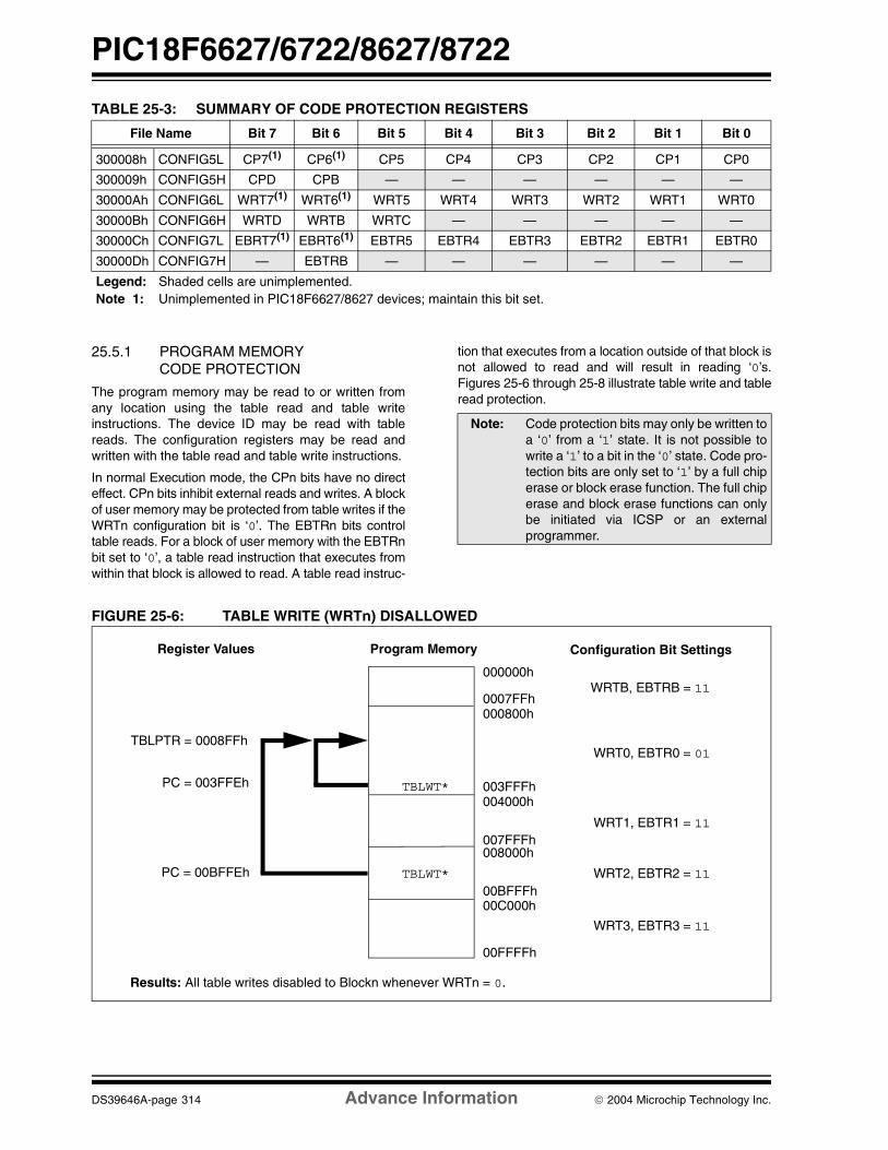
PIC18F6627/6722/8627/8722
DS39646A-page 314 Advance Information 2004 Microchip Technology Inc.
TABLE 25-3: SUMMARY OF CODE PROTECTION REGISTERS
25.5.1 PROGRAM MEMORYCODE PROTECTION
The program memory may be read to or written fromany location using the table read and table writeinstructions. The device ID may be read with tablereads. The configuration registers may be read andwritten with the table read and table write instructions.
In normal Execution mode, the CPn bits have no directeffect. CPn bits inhibit external reads and writes. A blockof user memory may be protected from table writes if theWRTn configuration bit is ‘0’. The EBTRn bits controltable reads. For a block of user memory with the EBTRnbit set to ‘0’, a table read instruction that executes fromwithin that block is allowed to read. A table read instruc-
tion that executes from a location outside of that block isnot allowed to read and will result in reading ‘0’s.Figures 25-6 through 25-8 illustrate table write and tableread protection.
FIGURE 25-6: TABLE WRITE (WRTn) DISALLOWED
File Name Bit 7 Bit 6 Bit 5 Bit 4 Bit 3 Bit 2 Bit 1 Bit 0
300008h CONFIG5L CP7(1) CP6(1) CP5 CP4 CP3 CP2 CP1 CP0
300009h CONFIG5H CPD CPB — — — — — —
30000Ah CONFIG6L WRT7(1) WRT6(1) WRT5 WRT4 WRT3 WRT2 WRT1 WRT0
30000Bh CONFIG6H WRTD WRTB WRTC — — — — —
30000Ch CONFIG7L EBRT7(1) EBRT6(1) EBTR5 EBTR4 EBTR3 EBTR2 EBTR1 EBTR0
30000Dh CONFIG7H — EBTRB — — — — — —
Legend: Shaded cells are unimplemented.Note 1: Unimplemented in PIC18F6627/8627 devices; maintain this bit set.
Note: Code protection bits may only be written toa ‘0’ from a ‘1’ state. It is not possible towrite a ‘1’ to a bit in the ‘0’ state. Code pro-tection bits are only set to ‘1’ by a full chiperase or block erase function. The full chiperase and block erase functions can onlybe initiated via ICSP or an externalprogrammer.
000000h
0007FFh000800h
003FFFh004000h
007FFFh008000h
00BFFFh00C000h
00FFFFh
WRTB, EBTRB = 11
WRT0, EBTR0 = 01
WRT1, EBTR1 = 11
WRT2, EBTR2 = 11
WRT3, EBTR3 = 11
TBLWT*
TBLPTR = 0008FFh
PC = 003FFEh
TBLWT*PC = 00BFFEh
Register Values Program Memory Configuration Bit Settings
Results: All table writes disabled to Blockn whenever WRTn = 0.

2004 Microchip Technology Inc. Advance Information DS39646A-page 315
PIC18F6627/6722/8627/8722
FIGURE 25-7: EXTERNAL BLOCK TABLE READ (EBTRn) DISALLOWED
FIGURE 25-8: EXTERNAL BLOCK TABLE READ (EBTRn) ALLOWED
WRTB, EBTRB = 11
WRT0, EBTR0 = 10
WRT1, EBTR1 = 11
WRT2, EBTR2 = 11
WRT3, EBTR3 = 11
TBLRD*
TBLPTR = 0008FFh
PC = 007FFEh
Results: All table reads from external blocks to Blockn are disabled whenever EBTRn = 0.TABLAT register returns a value of ‘0’.
Register Values Program Memory Configuration Bit Settings
000000h
0007FFh000800h
003FFFh004000h
007FFFh008000h
00BFFFh00C000h
00FFFFh
WRTB, EBTRB = 11
WRT0, EBTR0 = 10
WRT1, EBTR1 = 11
WRT2, EBTR2 = 11
WRT3, EBTR3 = 11
TBLRD*
TBLPTR = 0008FFh
PC = 003FFEh
Register Values Program Memory Configuration Bit Settings
Results: Table reads permitted within Blockn, even when EBTRBn = 0.TABLAT register returns the value of the data at the location TBLPTR.
000000h
0007FFh000800h
003FFFh004000h
007FFFh008000h
00BFFFh00C000h
00FFFFh

PIC18F6627/6722/8627/8722
DS39646A-page 316 Advance Information 2004 Microchip Technology Inc.
25.5.2 DATA EEPROM CODE PROTECTION
The entire data EEPROM is protected from externalreads and writes by two bits: CPD and WRTD. CPDinhibits external reads and writes of data EEPROM.WRTD inhibits internal and external writes to dataEEPROM. The CPU can always read data EEPROMunder normal operation, regardless of the protection bitsettings.
25.5.3 CONFIGURATION REGISTER PROTECTION
The configuration registers can be write-protected. TheWRTC bit controls protection of the configurationregisters. In normal Execution mode, the WRTC bit isreadable only. WRTC can only be written via ICSP oran external programmer.
25.6 ID Locations
Eight memory locations (200000h-200007h) aredesignated as ID locations, where the user can storechecksum or other code identification numbers. Theselocations are both readable and writable during normalexecution through the TBLRD and TBLWT instructionsor during program/verify. The ID locations can be readwhen the device is code-protected.
25.7 In-Circuit Serial Programming
PIC18F6627/6722/8627/8722 devices can be seriallyprogrammed while in the end application circuit. This issimply done with two lines for clock and data and threeother lines for power, ground and the programmingvoltage. This allows customers to manufacture boardswith unprogrammed devices and then program themicrocontroller just before shipping the product. Thisalso allows the most recent firmware or a customfirmware to be programmed.
25.8 In-Circuit Debugger
When the DEBUG configuration bit is programmed to a‘0’, the In-Circuit Debugger functionality is enabled.This function allows simple debugging functions whenused with MPLAB® IDE. When the microcontroller hasthis feature enabled, some resources are not availablefor general use. Table 25-4 shows which resources arerequired by the background debugger.
TABLE 25-4: DEBUGGER RESOURCES
To use the In-Circuit Debugger function of the micro-controller, the design must implement In-Circuit SerialProgramming connections to MCLR/VPP/RG5, VDD,VSS, RB7 and RB6. This will interface to the In-CircuitDebugger module available from Microchip or one ofthe third party development tool companies.
25.9 Single-Supply ICSP Programming
The LVP configuration bit enables Single-Supply ICSPProgramming (formerly known as Low-Voltage ICSPProgramming or LVP). When single-supply program-ming is enabled, the microcontroller can be programmedwithout requiring high voltage being applied to theMCLR/VPP/RG5 pin, but the RB5/KBI1/PGM pin is thendedicated to controlling Program mode entry and is notavailable as a general purpose I/O pin.
While programming, using single-supply programmingmode, VDD is applied to the MCLR/VPP/RG5 pin as innormal execution mode. To enter Programming mode,VDD is applied to the PGM pin.
If Single-Supply ICSP Programming mode will not beused, the LVP bit can be cleared. RB5/KBI1/PGM thenbecomes available as the digital I/O pin, RB5. The LVPbit may be set or cleared only when using standardhigh-voltage programming (VIHH applied to the MCLR/VPP/RG5 pin). Once LVP has been disabled, only thestandard high-voltage programming is available andmust be used to program the device.
Memory that is not code-protected can be erased usingeither a block erase, or erased row by row, then writtenat any specified VDD. If code-protected memory is to beerased, a block erase is required. If a block erase is tobe performed when using Low-Voltage Programming,the device must be supplied with VDD of 4.5V to 5.5V.
I/O pins: RB6, RB7
Stack: 2 levels
Program Memory: 512 bytes
Data Memory: 10 bytes
Note 1: High-voltage programming is alwaysavailable, regardless of the state of theLVP bit or the PGM pin, by applying VIHH
to the MCLR pin.
2: By default, single-supply ICSP is enabledin unprogrammed devices (as suppliedfrom Microchip) and erased devices.
3: When single-supply programming isenabled, the RB5 pin can no longer beused as a general purpose I/O pin.
4: When LVP is enabled, externally pull thePGM pin to VSS to allow normal programexecution.

2004 Microchip Technology Inc. Advance Information DS39646A-page 317
PIC18F6627/6722/8627/8722
26.0 INSTRUCTION SET SUMMARY
PIC18F6627/6722/8627/8722 devices incorporate thestandard set of 75 PIC18 core instructions, as well as anextended set of 8 new instructions, for the optimizationof code that is recursive or that utilizes a software stack.The extended set is discussed later in this section.
26.1 Standard Instruction Set
The standard PIC18 instruction set adds manyenhancements to the previous PICmicro® instructionsets, while maintaining an easy migration from thesePICmicro instruction sets. Most instructions are a sin-gle program memory word (16 bits), but there are fourinstructions that require two program memorylocations.
Each single-word instruction is a 16-bit word dividedinto an opcode, which specifies the instruction type andone or more operands, which further specify theoperation of the instruction.
The instruction set is highly orthogonal and is groupedinto four basic categories:
• Byte-oriented operations• Bit-oriented operations
• Literal operations• Control operations
The PIC18 instruction set summary in Table 26-2 listsbyte-oriented, bit-oriented, literal and controloperations. Table 26-1 shows the opcode fielddescriptions.
Most byte-oriented instructions have three operands:
1. The file register (specified by ‘f’) 2. The destination of the result (specified by ‘d’)
3. The accessed memory (specified by ‘a’)
The file register designator ‘f’ specifies which fileregister is to be used by the instruction. The destinationdesignator ‘d’ specifies where the result of the opera-tion is to be placed. If ‘d’ is zero, the result is placed inthe WREG register. If ‘d’ is one, the result is placed inthe file register specified in the instruction.
All bit-oriented instructions have three operands:
1. The file register (specified by ‘f’) 2. The bit in the file register (specified by ‘b’)
3. The accessed memory (specified by ‘a’)
The bit field designator ‘b’ selects the number of the bitaffected by the operation, while the file registerdesignator ‘f’ represents the number of the file in whichthe bit is located.
The literal instructions may use some of the followingoperands:
• A literal value to be loaded into a file register (specified by ‘k’)
• The desired FSR register to load the literal value into (specified by ‘f’)
• No operand required (specified by ‘—’)
The control instructions may use some of the followingoperands:
• A program memory address (specified by ‘n’)• The mode of the CALL or RETURN instructions
(specified by ‘s’)• The mode of the table read and table write
instructions (specified by ‘m’)• No operand required
(specified by ‘—’)
All instructions are a single word, except for fourdouble-word instructions. These instructions weremade double-word to contain the required informationin 32 bits. In the second word, the 4 MSbs are ‘1’s. Ifthis second word is executed as an instruction (byitself), it will execute as a NOP.
All single-word instructions are executed in a singleinstruction cycle, unless a conditional test is true or theprogram counter is changed as a result of the instruc-tion. In these cases, the execution takes two instructioncycles, with the additional instruction cycle(s) executedas a NOP.
The double-word instructions execute in two instructioncycles.
One instruction cycle consists of four oscillator periods.Thus, for an oscillator frequency of 4 MHz, the normalinstruction execution time is 1 µs. If a conditional test istrue, or the program counter is changed as a result ofan instruction, the instruction execution time is 2 µs.Two-word branch instructions (if true) would take 3 µs.
Figure 26-1 shows the general formats that the instruc-tions can have. All examples use the convention ‘nnh’to represent a hexadecimal number.
The Instruction Set Summary, shown in Table 26-2,lists the standard instructions recognized by theMicrochip Assembler (MPASMTM assembler).
Section 26.1.1 “Standard Instruction Set” providesa description of each instruction.
PIC18F6627/6722/8627/8722
DS39646A-page 318 Advance Information 2004 Microchip Technology Inc.
TABLE 26-1: OPCODE FIELD DESCRIPTIONS
Field Description
a RAM access bita = 0: RAM location in Access RAM (BSR register is ignored)a = 1: RAM bank is specified by BSR register
bbb Bit address within an 8-bit file register (0 to 7).
BSR Bank Select Register. Used to select the current RAM bank.
C, DC, Z, OV, N ALU Status bits: Carry, Digit Carry, Zero, Overflow, Negative.
d Destination select bitd = 0: store result in WREGd = 1: store result in file register f
dest Destination: either the WREG register or the specified register file location.
f 8-bit Register file address (00h to FFh) or 2-bit FSR designator (0h to 3h).
fs 12-bit Register file address (000h to FFFh). This is the source address.
fd 12-bit Register file address (000h to FFFh). This is the destination address.
GIE Global Interrupt Enable bit.
k Literal field, constant data or label (may be either an 8-bit, 12-bit or a 20-bit value).
label Label name.
mm The mode of the TBLPTR register for the table read and table write instructions.Only used with table read and table write instructions:
* No change to register (such as TBLPTR with table reads and writes)
*+ Post-Increment register (such as TBLPTR with table reads and writes)
*- Post-Decrement register (such as TBLPTR with table reads and writes)
+* Pre-Increment register (such as TBLPTR with table reads and writes)
n The relative address (2’s complement number) for relative branch instructions or the direct address for Call/Branch and Return instructions.
PC Program Counter.
PCL Program Counter Low Byte.
PCH Program Counter High Byte.
PCLATH Program Counter High Byte Latch.
PCLATU Program Counter Upper Byte Latch.
PD Power-down bit.
PRODH Product of Multiply High Byte.
PRODL Product of Multiply Low Byte.
s Fast Call/Return mode select bits = 0: do not update into/from shadow registerss = 1: certain registers loaded into/from shadow registers (Fast mode)
TBLPTR 21-bit Table Pointer (points to a Program Memory location).
TABLAT 8-bit Table Latch.
TO Time-out bit.
TOS Top-of-Stack.
u Unused or unchanged.
WDT Watchdog Timer.
WREG Working register (accumulator).
x Don’t care (‘0’ or ‘1’). The assembler will generate code with x = 0. It is the recommended form of use for compatibility with all Microchip software tools.
zs 7-bit offset value for indirect addressing of register files (source).
zd 7-bit offset value for indirect addressing of register files (destination).
Optional argument.
[text] Indicates an indexed address.
(text) The contents of text.
[expr]<n> Specifies bit n of the register indicated by the pointer expr.
→ Assigned to.
< > Register bit field.
∈ In the set of.
italics User defined term (font is Courier).

2004 Microchip Technology Inc. Advance Information DS39646A-page 319
PIC18F6627/6722/8627/8722
FIGURE 26-1: GENERAL FORMAT FOR INSTRUCTIONS
Byte-oriented file register operations
15 10 9 8 7 0
d = 0 for result destination to be WREG register
OPCODE d a f (FILE #)
d = 1 for result destination to be file register (f)a = 0 to force Access Bank
Bit-oriented file register operations
15 12 11 9 8 7 0
OPCODE b (BIT #) a f (FILE #)
b = 3-bit position of bit in file register (f)
Literal operations
15 8 7 0
OPCODE k (literal)
k = 8-bit immediate value
Byte to Byte move operations (2-word)
15 12 11 0
OPCODE f (Source FILE #)
CALL, GOTO and Branch operations
15 8 7 0
OPCODE n<7:0> (literal)
n = 20-bit immediate value
a = 1 for BSR to select bankf = 8-bit file register address
a = 0 to force Access Banka = 1 for BSR to select bankf = 8-bit file register address
15 12 11 0
1111 n<19:8> (literal)
15 12 11 0
1111 f (Destination FILE #)
f = 12-bit file register address
Control operations
Example Instruction
ADDWF MYREG, W, B
MOVFF MYREG1, MYREG2
BSF MYREG, bit, B
MOVLW 7Fh
GOTO Label
15 8 7 0
OPCODE n<7:0> (literal)
15 12 11 0
1111 n<19:8> (literal)
CALL MYFUNC
15 11 10 0
OPCODE n<10:0> (literal)
S = Fast bit
BRA MYFUNC
15 8 7 0
OPCODE n<7:0> (literal) BC MYFUNC
S

PIC18F6627/6722/8627/8722
DS39646A-page 320 Advance Information 2004 Microchip Technology Inc.
TABLE 26-2: PIC18FXXXX INSTRUCTION SET
Mnemonic,Operands
Description Cycles16-Bit Instruction Word Status
AffectedNotes
MSb LSb
BYTE-ORIENTED OPERATIONS
ADDWFADDWFCANDWFCLRFCOMFCPFSEQCPFSGTCPFSLTDECFDECFSZDCFSNZINCFINCFSZINFSNZIORWFMOVFMOVFF
MOVWFMULWFNEGFRLCFRLNCFRRCFRRNCFSETFSUBFWB
SUBWFSUBWFB
SWAPFTSTFSZXORWF
f, d, af, d, af, d, af, af, d, af, af, af, af, d, af, d, af, d, af, d, af, d, af, d, af, d, af, d, afs, fd
f, af, af, af, d, af, d, af, d, af, d, af, af, d, a
f, d, af, d, a
f, d, af, af, d, a
Add WREG and fAdd WREG and CARRY bit to fAND WREG with fClear fComplement fCompare f with WREG, skip =Compare f with WREG, skip >Compare f with WREG, skip <Decrement fDecrement f, Skip if 0Decrement f, Skip if Not 0Increment fIncrement f, Skip if 0Increment f, Skip if Not 0Inclusive OR WREG with fMove fMove fs (source) to 1st word
fd (destination) 2nd wordMove WREG to fMultiply WREG with fNegate fRotate Left f through CarryRotate Left f (No Carry)Rotate Right f through CarryRotate Right f (No Carry)Set fSubtract f from WREG with borrow Subtract WREG from fSubtract WREG from f with borrowSwap nibbles in fTest f, skip if 0Exclusive OR WREG with f
111111 (2 or 3)1 (2 or 3)1 (2 or 3)11 (2 or 3)1 (2 or 3)11 (2 or 3)1 (2 or 3)112
111111111
11
11 (2 or 3)1
001000100001011000010110011001100000001001000010001101000001010111001111011000000110001101000011010001100101
01010101
001101100001
01da00da01da101a11da001a010a000a01da11da11da10da11da10da00da00daffffffff111a001a110a01da01da00da00da100a01da
11da10da
10da011a10da
ffffffffffffffffffffffffffffffffffffffffffffffffffffffffffffffffffffffffffffffffffffffffffffffffffffffffffff
ffffffff
ffffffffffff
ffffffffffffffffffffffffffffffffffffffffffffffffffffffffffffffffffffffffffffffffffffffffffffffffffffffffffff
ffffffff
ffffffffffff
C, DC, Z, OV, NC, DC, Z, OV, NZ, NZZ, NNoneNoneNoneC, DC, Z, OV, NNoneNoneC, DC, Z, OV, NNoneNoneZ, NZ, NNone
NoneNoneC, DC, Z, OV, NC, Z, NZ, NC, Z, NZ, NNoneC, DC, Z, OV, N
C, DC, Z, OV, NC, DC, Z, OV, N
NoneNoneZ, N
1, 21, 21,221, 2441, 21, 2, 3, 41, 2, 3, 41, 21, 2, 3, 441, 21, 21
1, 2
1, 2
1, 2
1, 2
41, 2
Note 1: When a Port register is modified as a function of itself (e.g., MOVF PORTB, 1, 0), the value used will be that value present on the pins themselves. For example, if the data latch is ‘1’ for a pin configured as input and is driven low by an external device, the data will be written back with a ‘0’.
2: If this instruction is executed on the TMR0 register (and where applicable, ‘d’ = 1), the prescaler will be cleared if assigned.
3: If Program Counter (PC) is modified or a conditional test is true, the instruction requires two cycles. The second cycle is executed as a NOP.
4: Some instructions are two-word instructions. The second word of these instructions will be executed as a NOP unless the first word of the instruction retrieves the information embedded in these 16 bits. This ensures that all program memory locations have a valid instruction.

2004 Microchip Technology Inc. Advance Information DS39646A-page 321
PIC18F6627/6722/8627/8722
BIT-ORIENTED OPERATIONS
BCFBSFBTFSCBTFSSBTG
f, b, af, b, af, b, af, b, af, b, a
Bit Clear fBit Set fBit Test f, Skip if ClearBit Test f, Skip if SetBit Toggle f
111 (2 or 3)1 (2 or 3)1
10011000101110100111
bbbabbbabbbabbbabbba
ffffffffffffffffffff
ffffffffffffffffffff
NoneNoneNoneNoneNone
1, 21, 23, 43, 41, 2
CONTROL OPERATIONS
BCBNBNCBNNBNOVBNZBOVBRABZCALL
CLRWDTDAWGOTO
NOPNOPPOPPUSHRCALLRESETRETFIE
RETLWRETURNSLEEP
nnnnnnnnnn, s
——n
————n
s
ks—
Branch if CarryBranch if NegativeBranch if Not CarryBranch if Not NegativeBranch if Not OverflowBranch if Not ZeroBranch if OverflowBranch Unconditionally Branch if ZeroCall subroutine 1st word
2nd wordClear Watchdog TimerDecimal Adjust WREGGo to address 1st word
2nd wordNo OperationNo OperationPop top of return stack (TOS)Push top of return stack (TOS)Relative CallSoftware device ResetReturn from interrupt enable
Return with literal in WREG Return from SubroutineGo into Standby mode
1 (2)1 (2)1 (2)1 (2)1 (2)1 (2)1 (2)21 (2)2
112
1111212
221
1110111011101110111011101110110111101110111100000000111011110000111100000000110100000000
000000000000
00100110001101110101000101000nnn0000110skkkk000000001111kkkk0000xxxx000000001nnn00000000
110000000000
nnnnnnnnnnnnnnnnnnnnnnnnnnnnnnnnnnnnkkkkkkkk00000000kkkkkkkk0000xxxx00000000nnnn11110001
kkkk00010000
nnnnnnnnnnnnnnnnnnnnnnnnnnnnnnnnnnnnkkkkkkkk01000111kkkkkkkk0000xxxx01100101nnnn1111000s
kkkk001s0011
NoneNoneNoneNoneNoneNoneNoneNoneNoneNone
TO, PDCNone
NoneNoneNoneNoneNoneAllGIE/GIEH, PEIE/GIELNoneNoneTO, PD
4
TABLE 26-2: PIC18FXXXX INSTRUCTION SET (CONTINUED)
Mnemonic,Operands
Description Cycles16-Bit Instruction Word Status
AffectedNotes
MSb LSb
Note 1: When a Port register is modified as a function of itself (e.g., MOVF PORTB, 1, 0), the value used will be that value present on the pins themselves. For example, if the data latch is ‘1’ for a pin configured as input and is driven low by an external device, the data will be written back with a ‘0’.
2: If this instruction is executed on the TMR0 register (and where applicable, ‘d’ = 1), the prescaler will be cleared if assigned.
3: If Program Counter (PC) is modified or a conditional test is true, the instruction requires two cycles. The second cycle is executed as a NOP.
4: Some instructions are two-word instructions. The second word of these instructions will be executed as a NOP unless the first word of the instruction retrieves the information embedded in these 16 bits. This ensures that all program memory locations have a valid instruction.

PIC18F6627/6722/8627/8722
DS39646A-page 322 Advance Information 2004 Microchip Technology Inc.
LITERAL OPERATIONS
ADDLWANDLWIORLWLFSR
MOVLBMOVLWMULLWRETLWSUBLWXORLW
kkkf, k
kkkkkk
Add literal and WREGAND literal with WREGInclusive OR literal with WREGMove literal (12-bit) 2nd word to FSR(f) 1st wordMove literal to BSR<3:0>Move literal to WREGMultiply literal with WREGReturn with literal in WREG Subtract WREG from literalExclusive OR literal with WREG
1112
111211
00000000000011101111000000000000000000000000
11111011100111100000000111101101110010001010
kkkkkkkkkkkk00ffkkkk0000kkkkkkkkkkkkkkkkkkkk
kkkkkkkkkkkkkkkkkkkkkkkkkkkkkkkkkkkkkkkkkkkk
C, DC, Z, OV, NZ, NZ, NNone
NoneNoneNoneNoneC, DC, Z, OV, NZ, N
DATA MEMORY ↔ PROGRAM MEMORY OPERATIONS
TBLRD*TBLRD*+TBLRD*-TBLRD+*TBLWT*TBLWT*+TBLWT*-TBLWT+*
Table ReadTable Read with post-incrementTable Read with post-decrementTable Read with pre-incrementTable WriteTable Write with post-incrementTable Write with post-decrementTable Write with pre-increment
2
2
00000000000000000000000000000000
00000000000000000000000000000000
00000000000000000000000000000000
10001001101010111100110111101111
NoneNoneNoneNoneNoneNoneNoneNone
TABLE 26-2: PIC18FXXXX INSTRUCTION SET (CONTINUED)
Mnemonic,Operands
Description Cycles16-Bit Instruction Word Status
AffectedNotes
MSb LSb
Note 1: When a Port register is modified as a function of itself (e.g., MOVF PORTB, 1, 0), the value used will be that value present on the pins themselves. For example, if the data latch is ‘1’ for a pin configured as input and is driven low by an external device, the data will be written back with a ‘0’.
2: If this instruction is executed on the TMR0 register (and where applicable, ‘d’ = 1), the prescaler will be cleared if assigned.
3: If Program Counter (PC) is modified or a conditional test is true, the instruction requires two cycles. The second cycle is executed as a NOP.
4: Some instructions are two-word instructions. The second word of these instructions will be executed as a NOP unless the first word of the instruction retrieves the information embedded in these 16 bits. This ensures that all program memory locations have a valid instruction.
2004 Microchip Technology Inc. Advance Information DS39646A-page 323
PIC18F6627/6722/8627/8722
26.1.1 STANDARD INSTRUCTION SET
ADDLW ADD literal to W
Syntax: ADDLW k
Operands: 0 ≤ k ≤ 255
Operation: (W) + k → W
Status Affected: N, OV, C, DC, Z
Encoding: 0000 1111 kkkk kkkk
Description: The contents of W are added to the 8-bit literal ‘k’ and the result is placed in W.
Words: 1
Cycles: 1
Q Cycle Activity:
Q1 Q2 Q3 Q4
Decode Readliteral ‘k’
Process Data
Write to W
Example: ADDLW 15h
Before Instruction
W = 10hAfter Instruction
W = 25h
ADDWF ADD W to f
Syntax: ADDWF f ,d ,a
Operands: 0 ≤ f ≤ 255d ∈ [0,1]a ∈ [0,1]
Operation: (W) + (f) → dest
Status Affected: N, OV, C, DC, Z
Encoding: 0010 01da ffff ffff
Description: Add W to register ‘f’. If ‘d’ is ‘0’, the result is stored in W. If ‘d’ is ‘1’, the result is stored back in register ‘f’ (default). If ‘a’ is ‘0’, the Access Bank is selected. If ‘a’ is ‘1’, the BSR is used to select the GPR bank (default). If ‘a’ is ‘0’ and the extended instruction set is enabled, this instruction operates in Indexed Literal Offset Addressing mode whenever f ≤ 95 (5Fh). See Section 26.2.3 “Byte-Oriented and Bit-Oriented Instructions in Indexed Literal Offset Mode” for details.
Words: 1
Cycles: 1
Q Cycle Activity:
Q1 Q2 Q3 Q4
Decode Readregister ‘f’
Process Data
Write todestination
Example: ADDWF REG, 0, 0
Before Instruction
W = 17hREG = 0C2h
After Instruction
W = 0D9hREG = 0C2h
Note: All PIC18 instructions may take an optional label argument preceding the instruction mnemonic for use insymbolic addressing. If a label is used, the instruction format then becomes: label instruction argument(s).

PIC18F6627/6722/8627/8722
DS39646A-page 324 Advance Information 2004 Microchip Technology Inc.
ADDWFC ADD W and CARRY bit to f
Syntax: ADDWFC f ,d ,a
Operands: 0 ≤ f ≤ 255d ∈ [0,1]a ∈ [0,1]
Operation: (W) + (f) + (C) → dest
Status Affected: N,OV, C, DC, Z
Encoding: 0010 00da ffff ffff
Description: Add W, the CARRY flag and data mem-ory location ‘f’. If ‘d’ is ‘0’, the result is placed in W. If ‘d’ is ‘1’, the result is placed in data memory location ‘f’. If ‘a’ is ‘0’, the Access Bank is selected. If ‘a’ is ‘1’, the BSR is used to select the GPR bank (default). If ‘a’ is ‘0’ and the extended instruction set is enabled, this instruction operates in Indexed Literal Offset Addressing mode whenever f ≤ 95 (5Fh). See Section 26.2.3 “Byte-Oriented and Bit-Oriented Instructions in Indexed Literal Offset Mode” for details.
Words: 1
Cycles: 1
Q Cycle Activity:
Q1 Q2 Q3 Q4
Decode Readregister ‘f’
Process Data
Write to destination
Example: ADDWFC REG, 0, 1
Before InstructionCARRY bit = 1REG = 02hW = 4Dh
After InstructionCARRY bit = 0REG = 02hW = 50h
ANDLW AND literal with W
Syntax: ANDLW k
Operands: 0 ≤ k ≤ 255
Operation: (W) .AND. k → W
Status Affected: N, Z
Encoding: 0000 1011 kkkk kkkk
Description: The contents of W are AND’ed with the 8-bit literal ‘k’. The result is placed in W.
Words: 1
Cycles: 1
Q Cycle Activity:
Q1 Q2 Q3 Q4
Decode Read literal ‘k’
Process Data
Write to W
Example: ANDLW 05Fh
Before Instruction
W = A3hAfter Instruction
W = 03h

2004 Microchip Technology Inc. Advance Information DS39646A-page 325
PIC18F6627/6722/8627/8722
ANDWF AND W with f
Syntax: ANDWF f ,d ,a
Operands: 0 ≤ f ≤ 255d ∈ [0,1]a ∈ [0,1]
Operation: (W) .AND. (f) → dest
Status Affected: N, Z
Encoding: 0001 01da ffff ffff
Description: The contents of W are AND’ed with register ‘f’. If ‘d’ is ‘0’, the result is stored in W. If ‘d’ is ‘1’, the result is stored back in register ‘f’ (default). If ‘a’ is ‘0’, the Access Bank is selected. If ‘a’ is ‘1’, the BSR is used to select the GPR bank (default). If ‘a’ is ‘0’ and the extended instruction set is enabled, this instruction operates in Indexed Literal Offset Addressing mode whenever f ≤ 95 (5Fh). See Section 26.2.3 “Byte-Oriented and Bit-Oriented Instructions in Indexed Literal Offset Mode” for details.
Words: 1
Cycles: 1
Q Cycle Activity:
Q1 Q2 Q3 Q4
Decode Readregister ‘f’
Process Data
Write to destination
Example: ANDWF REG, 0, 0
Before Instruction
W = 17hREG = C2h
After Instruction
W = 02hREG = C2h
BC Branch if Carry
Syntax: BC n
Operands: -128 ≤ n ≤ 127
Operation: if CARRY bit is ‘1’(PC) + 2 + 2n → PC
Status Affected: None
Encoding: 1110 0010 nnnn nnnn
Description: If the CARRY bit is ‘1’, then the program will branch.The 2’s complement number ‘2n’ is added to the PC. Since the PC will have incremented to fetch the next instruction, the new address will be PC + 2 + 2n. This instruction is then a two-cycle instruction.
Words: 1
Cycles: 1(2)
Q Cycle Activity:If Jump:
Q1 Q2 Q3 Q4
Decode Read literal ‘n’
Process Data
Write to PC
No operation
No operation
No operation
No operation
If No Jump:
Q1 Q2 Q3 Q4
Decode Read literal ‘n’
Process Data
No operation
Example: HERE BC 5
Before InstructionPC = address (HERE)
After InstructionIf CARRY = 1;
PC = address (HERE + 12)If CARRY = 0;
PC = address (HERE + 2)

PIC18F6627/6722/8627/8722
DS39646A-page 326 Advance Information 2004 Microchip Technology Inc.
BCF Bit Clear f
Syntax: BCF f, b ,a
Operands: 0 ≤ f ≤ 2550 ≤ b ≤ 7a ∈ [0,1]
Operation: 0 → f<b>
Status Affected: None
Encoding: 1001 bbba ffff ffff
Description: Bit ‘b’ in register ‘f’ is cleared.If ‘a’ is ‘0’, the Access Bank is selected. If ‘a’ is ‘1’, the BSR is used to select the GPR bank (default). If ‘a’ is ‘0’ and the extended instruction set is enabled, this instruction operates in Indexed Literal Offset Addressing mode whenever f ≤ 95 (5Fh). See Section 26.2.3 “Byte-Oriented and Bit-Oriented Instructions in Indexed Literal Offset Mode” for details.
Words: 1
Cycles: 1
Q Cycle Activity:
Q1 Q2 Q3 Q4
Decode Readregister ‘f’
Process Data
Writeregister ‘f’
Example: BCF FLAG_REG, 7, 0
Before InstructionFLAG_REG = C7h
After InstructionFLAG_REG = 47h
BN Branch if Negative
Syntax: BN n
Operands: -128 ≤ n ≤ 127
Operation: if NEGATIVE bit is ‘1’(PC) + 2 + 2n → PC
Status Affected: None
Encoding: 1110 0110 nnnn nnnn
Description: If the NEGATIVE bit is ‘1’, then the program will branch.The 2’s complement number ‘2n’ is added to the PC. Since the PC will have incremented to fetch the next instruction, the new address will be PC + 2 + 2n. This instruction is then a two-cycle instruction.
Words: 1
Cycles: 1(2)
Q Cycle Activity:If Jump:
Q1 Q2 Q3 Q4
Decode Read literal ‘n’
Process Data
Write to PC
No operation
No operation
No operation
No operation
If No Jump:
Q1 Q2 Q3 Q4
Decode Read literal ‘n’
Process Data
No operation
Example: HERE BN Jump
Before InstructionPC = address (HERE)
After InstructionIf NEGATIVE = 1;
PC = address (Jump)If NEGATIVE = 0;
PC = address (HERE + 2)

2004 Microchip Technology Inc. Advance Information DS39646A-page 327
PIC18F6627/6722/8627/8722
BNC Branch if Not Carry
Syntax: BNC n
Operands: -128 ≤ n ≤ 127
Operation: if CARRY bit is ‘0’(PC) + 2 + 2n → PC
Status Affected: None
Encoding: 1110 0011 nnnn nnnn
Description: If the CARRY bit is ‘0’, then the program will branch.The 2’s complement number ‘2n’ is added to the PC. Since the PC will have incremented to fetch the next instruction, the new address will be PC + 2 + 2n. This instruction is then a two-cycle instruction.
Words: 1
Cycles: 1(2)
Q Cycle Activity:If Jump:
Q1 Q2 Q3 Q4
Decode Read literal ‘n’
Process Data
Write to PC
No operation
No operation
No operation
No operation
If No Jump:
Q1 Q2 Q3 Q4
Decode Read literal ‘n’
Process Data
No operation
Example: HERE BNC Jump
Before InstructionPC = address (HERE)
After InstructionIf CARRY = 0;
PC = address (Jump)If CARRY = 1;
PC = address (HERE + 2)
BNN Branch if Not Negative
Syntax: BNN n
Operands: -128 ≤ n ≤ 127
Operation: if NEGATIVE bit is ‘0’(PC) + 2 + 2n → PC
Status Affected: None
Encoding: 1110 0111 nnnn nnnn
Description: If the NEGATIVE bit is ‘0’, then the program will branch.The 2’s complement number ‘2n’ is added to the PC. Since the PC will have incremented to fetch the next instruction, the new address will be PC + 2 + 2n. This instruction is then a two-cycle instruction.
Words: 1
Cycles: 1(2)
Q Cycle Activity:If Jump:
Q1 Q2 Q3 Q4
Decode Read literal ‘n’
Process Data
Write to PC
No operation
No operation
No operation
No operation
If No Jump:
Q1 Q2 Q3 Q4
Decode Read literal ‘n’
Process Data
No operation
Example: HERE BNN Jump
Before InstructionPC = address (HERE)
After InstructionIf NEGATIVE = 0;
PC = address (Jump)If NEGATIVE = 1;
PC = address (HERE + 2)

PIC18F6627/6722/8627/8722
DS39646A-page 328 Advance Information 2004 Microchip Technology Inc.
BNOV Branch if Not Overflow
Syntax: BNOV n
Operands: -128 ≤ n ≤ 127
Operation: if OVERFLOW bit is ‘0’(PC) + 2 + 2n → PC
Status Affected: None
Encoding: 1110 0101 nnnn nnnn
Description: If the OVERFLOW bit is ‘0’, then the program will branch.The 2’s complement number ‘2n’ is added to the PC. Since the PC will have incremented to fetch the next instruction, the new address will be PC + 2 + 2n. This instruction is then a two-cycle instruction.
Words: 1
Cycles: 1(2)
Q Cycle Activity:If Jump:
Q1 Q2 Q3 Q4
Decode Read literal ‘n’
Process Data
Write to PC
No operation
No operation
No operation
No operation
If No Jump:
Q1 Q2 Q3 Q4
Decode Read literal ‘n’
Process Data
No operation
Example: HERE BNOV Jump
Before InstructionPC = address (HERE)
After InstructionIf OVERFLOW = 0;
PC = address (Jump)If OVERFLOW = 1;
PC = address (HERE + 2)
BNZ Branch if Not Zero
Syntax: BNZ n
Operands: -128 ≤ n ≤ 127
Operation: if ZERO bit is ‘0’(PC) + 2 + 2n → PC
Status Affected: None
Encoding: 1110 0001 nnnn nnnn
Description: If the ZERO bit is ‘0’, then the program will branch.The 2’s complement number ‘2n’ is added to the PC. Since the PC will have incremented to fetch the next instruction, the new address will be PC + 2 + 2n. This instruction is then a two-cycle instruction.
Words: 1
Cycles: 1(2)
Q Cycle Activity:If Jump:
Q1 Q2 Q3 Q4
Decode Read literal ‘n’
Process Data
Write to PC
No operation
No operation
No operation
No operation
If No Jump:
Q1 Q2 Q3 Q4
Decode Read literal ‘n’
Process Data
No operation
Example: HERE BNZ Jump
Before InstructionPC = address (HERE)
After InstructionIf ZERO = 0;
PC = address (Jump)If ZERO = 1;
PC = address (HERE + 2)

2004 Microchip Technology Inc. Advance Information DS39646A-page 329
PIC18F6627/6722/8627/8722
BRA Unconditional Branch
Syntax: BRA n
Operands: -1024 ≤ n ≤ 1023
Operation: (PC) + 2 + 2n → PC
Status Affected: None
Encoding: 1101 0nnn nnnn nnnn
Description: Add the 2’s complement number ‘2n’ to the PC. Since the PC will have incre-mented to fetch the next instruction, the new address will be PC + 2 + 2n. This instruction is a two-cycle instruction.
Words: 1
Cycles: 2
Q Cycle Activity:
Q1 Q2 Q3 Q4
Decode Read literal ‘n’
Process Data
Write to PC
No operation
No operation
No operation
No operation
Example: HERE BRA Jump
Before InstructionPC = address (HERE)
After InstructionPC = address (Jump)
BSF Bit Set f
Syntax: BSF f, b ,a
Operands: 0 ≤ f ≤ 2550 ≤ b ≤ 7a ∈ [0,1]
Operation: 1 → f<b>
Status Affected: None
Encoding: 1000 bbba ffff ffff
Description: Bit ‘b’ in register ‘f’ is set. If ‘a’ is ‘0’, the Access Bank is selected. If ‘a’ is ‘1’, the BSR is used to select the GPR bank (default). If ‘a’ is ‘0’ and the extended instruction set is enabled, this instruction operates in Indexed Literal Offset Addressing mode whenever f ≤ 95 (5Fh). See Section 26.2.3 “Byte-Oriented and Bit-Oriented Instructions in Indexed Literal Offset Mode” for details.
Words: 1
Cycles: 1
Q Cycle Activity:
Q1 Q2 Q3 Q4
Decode Readregister ‘f’
Process Data
Writeregister ‘f’
Example: BSF FLAG_REG, 7, 1
Before InstructionFLAG_REG = 0Ah
After InstructionFLAG_REG = 8Ah

PIC18F6627/6722/8627/8722
DS39646A-page 330 Advance Information 2004 Microchip Technology Inc.
BTFSC Bit Test File, Skip if Clear
Syntax: BTFSC f, b ,a
Operands: 0 ≤ f ≤ 2550 ≤ b ≤ 7a ∈ [0,1]
Operation: skip if (f<b>) = 0
Status Affected: None
Encoding: 1011 bbba ffff ffff
Description: If bit ‘b’ in register ‘f’ is ‘0’, then the next instruction is skipped. If bit ‘b’ is ‘0’, then the next instruction fetched during the current instruction execution is discarded and a NOP is executed instead, making this a two-cycle instruction. If ‘a’ is ‘0’, the Access Bank is selected. If ‘a’ is ‘1’, the BSR is used to select the GPR bank (default). If ‘a’ is ‘0’ and the extended instruction set is enabled, this instruction operates in Indexed Literal Offset Addressing mode whenever f ≤ 95 (5Fh). See Section 26.2.3 “Byte-Oriented and Bit-Oriented Instructions in Indexed Literal Offset Mode” for details.
Words: 1
Cycles: 1(2)Note: 3 cycles if skip and followed
by a 2-word instruction.
Q Cycle Activity:
Q1 Q2 Q3 Q4
Decode Readregister ‘f’
Process Data
No operation
If skip:
Q1 Q2 Q3 Q4
No operation
No operation
No operation
No operation
If skip and followed by 2-word instruction:
Q1 Q2 Q3 Q4
No operation
No operation
No operation
No operation
No operation
No operation
No operation
No operation
Example: HEREFALSETRUE
BTFSC::
FLAG, 1, 0
Before InstructionPC = address (HERE)
After InstructionIf FLAG<1> = 0;
PC = address (TRUE)If FLAG<1> = 1;
PC = address (FALSE)
BTFSS Bit Test File, Skip if Set
Syntax: BTFSS f, b ,a
Operands: 0 ≤ f ≤ 2550 ≤ b < 7a ∈ [0,1]
Operation: skip if (f<b>) = 1
Status Affected: None
Encoding: 1010 bbba ffff ffff
Description: If bit ‘b’ in register ‘f’ is ‘1’, then the next instruction is skipped. If bit ‘b’ is ‘1’, then the next instruction fetched during the current instruction execution is discarded and a NOP is executed instead, making this a two-cycle instruction. If ‘a’ is ‘0’, the Access Bank is selected. If ‘a’ is ‘1’, the BSR is used to select the GPR bank (default). If ‘a’ is ‘0’ and the extended instruction set is enabled, this instruction operates in Indexed Literal Offset Addressing mode whenever f ≤ 95 (5Fh). See Section 26.2.3 “Byte-Oriented and Bit-Oriented Instructions in Indexed Literal Offset Mode” for details.
Words: 1
Cycles: 1(2)Note: 3 cycles if skip and followed
by a 2-word instruction.
Q Cycle Activity:
Q1 Q2 Q3 Q4
Decode Readregister ‘f’
Process Data
No operation
If skip:
Q1 Q2 Q3 Q4
No operation
No operation
No operation
No operation
If skip and followed by 2-word instruction:
Q1 Q2 Q3 Q4
No operation
No operation
No operation
No operation
No operation
No operation
No operation
No operation
Example: HEREFALSETRUE
BTFSS::
FLAG, 1, 0
Before InstructionPC = address (HERE)
After InstructionIf FLAG<1> = 0;
PC = address (FALSE)If FLAG<1> = 1;
PC = address (TRUE)

2004 Microchip Technology Inc. Advance Information DS39646A-page 331
PIC18F6627/6722/8627/8722
BTG Bit Toggle f
Syntax: BTG f, b ,a
Operands: 0 ≤ f ≤ 2550 ≤ b < 7a ∈ [0,1]
Operation: (f<b>) → f<b>
Status Affected: None
Encoding: 0111 bbba ffff ffff
Description: Bit ‘b’ in data memory location ‘f’ is inverted.If ‘a’ is ‘0’, the Access Bank is selected. If ‘a’ is ‘1’, the BSR is used to select the GPR bank (default). If ‘a’ is ‘0’ and the extended instruction set is enabled, this instruction operates in Indexed Literal Offset Addressing mode whenever f ≤ 95 (5Fh). See Section 26.2.3 “Byte-Oriented and Bit-Oriented Instructions in Indexed Literal Offset Mode” for details.
Words: 1
Cycles: 1
Q Cycle Activity:
Q1 Q2 Q3 Q4
Decode Readregister ‘f’
Process Data
Writeregister ‘f’
Example: BTG PORTC, 4, 0
Before Instruction:PORTC = 0111 0101 [75h]
After Instruction:PORTC = 0110 0101 [65h]
BOV Branch if Overflow
Syntax: BOV n
Operands: -128 ≤ n ≤ 127
Operation: if OVERFLOW bit is ‘1’(PC) + 2 + 2n → PC
Status Affected: None
Encoding: 1110 0100 nnnn nnnn
Description: If the OVERFLOW bit is ‘1’, then the program will branch.The 2’s complement number ‘2n’ is added to the PC. Since the PC will have incremented to fetch the next instruction, the new address will be PC + 2 + 2n. This instruction is then a two-cycle instruction.
Words: 1
Cycles: 1(2)
Q Cycle Activity:If Jump:
Q1 Q2 Q3 Q4
Decode Read literal ‘n’
Process Data
Write to PC
No operation
No operation
No operation
No operation
If No Jump:
Q1 Q2 Q3 Q4
Decode Read literal ‘n’
Process Data
No operation
Example: HERE BOV Jump
Before InstructionPC = address (HERE)
After InstructionIf OVERFLOW = 1;
PC = address (Jump)If OVERFLOW = 0;
PC = address (HERE + 2)

PIC18F6627/6722/8627/8722
DS39646A-page 332 Advance Information 2004 Microchip Technology Inc.
BZ Branch if Zero
Syntax: BZ n
Operands: -128 ≤ n ≤ 127
Operation: if ZERO bit is ‘1’(PC) + 2 + 2n → PC
Status Affected: None
Encoding: 1110 0000 nnnn nnnn
Description: If the ZERO bit is ‘1’, then the program will branch.The 2’s complement number ‘2n’ is added to the PC. Since the PC will have incremented to fetch the next instruction, the new address will be PC + 2 + 2n. This instruction is then a two-cycle instruction.
Words: 1
Cycles: 1(2)
Q Cycle Activity:If Jump:
Q1 Q2 Q3 Q4
Decode Read literal ‘n’
Process Data
Write to PC
No operation
No operation
No operation
No operation
If No Jump:
Q1 Q2 Q3 Q4
Decode Read literal ‘n’
Process Data
No operation
Example: HERE BZ Jump
Before InstructionPC = address (HERE)
After InstructionIf ZERO = 1;
PC = address (Jump)If ZERO = 0;
PC = address (HERE + 2)
CALL Subroutine Call
Syntax: CALL k ,s
Operands: 0 ≤ k ≤ 1048575s ∈ [0,1]
Operation: (PC) + 4 → TOS,k → PC<20:1>,if s = 1(W) → WS,(Status) → STATUSS,(BSR) → BSRS
Status Affected: None
Encoding:1st word (k<7:0>)2nd word(k<19:8>)
11101111
110sk19kkk
k7kkkkkkk
kkkk0kkkk8
Description: Subroutine call of entire 2-Mbyte memory range. First, return address (PC + 4) is pushed onto the return stack. If ‘s’ = 1, the W, Status and BSR registers are also pushed into their respective shadow registers, WS, STATUSS and BSRS. If ‘s’ = 0, no update occurs (default). Then, the 20-bit value ‘k’ is loaded into PC<20:1>. CALL is a two-cycle instruction.
Words: 2
Cycles: 2
Q Cycle Activity:
Q1 Q2 Q3 Q4
Decode Read literal ‘k’<7:0>,
PUSH PC to stack
Read literal ‘k’<19:8>,
Write to PC
No operation
No operation
No operation
No operation
Example: HERE CALL THERE, 1
Before InstructionPC = address (HERE)
After InstructionPC = address (THERE)TOS = address (HERE + 4)WS = WBSRS = BSRSTATUSS = Status

2004 Microchip Technology Inc. Advance Information DS39646A-page 333
PIC18F6627/6722/8627/8722
CLRF Clear f
Syntax: CLRF f ,a
Operands: 0 ≤ f ≤ 255a ∈ [0,1]
Operation: 000h → f1 → Z
Status Affected: Z
Encoding: 0110 101a ffff ffff
Description: Clears the contents of the specified register. If ‘a’ is ‘0’, the Access Bank is selected. If ‘a’ is ‘1’, the BSR is used to select the GPR bank (default). If ‘a’ is ‘0’ and the extended instruction set is enabled, this instruction operates in Indexed Literal Offset Addressing mode whenever f ≤ 95 (5Fh). See Section 26.2.3 “Byte-Oriented and Bit-Oriented Instructions in Indexed Literal Offset Mode” for details.
Words: 1
Cycles: 1
Q Cycle Activity:
Q1 Q2 Q3 Q4
Decode Readregister ‘f’
Process Data
Writeregister ‘f’
Example: CLRF FLAG_REG, 1
Before InstructionFLAG_REG = 5Ah
After InstructionFLAG_REG = 00h
CLRWDT Clear Watchdog Timer
Syntax: CLRWDT
Operands: None
Operation: 000h → WDT,000h → WDT postscaler,1 → TO,1 → PD
Status Affected: TO, PD
Encoding: 0000 0000 0000 0100
Description: CLRWDT instruction resets the Watchdog Timer. It also resets the postscaler of the WDT. Status bits, TO and PD, are set.
Words: 1
Cycles: 1
Q Cycle Activity:
Q1 Q2 Q3 Q4
Decode Nooperation
Process Data
No operation
Example: CLRWDT
Before InstructionWDT Counter = ?
After InstructionWDT Counter = 00hWDT Postscaler = 0TO = 1PD = 1

PIC18F6627/6722/8627/8722
DS39646A-page 334 Advance Information 2004 Microchip Technology Inc.
COMF Complement f
Syntax: COMF f ,d ,a
Operands: 0 ≤ f ≤ 255d ∈ [0,1]a ∈ [0,1]
Operation: (f) → dest
Status Affected: N, Z
Encoding: 0001 11da ffff ffff
Description: The contents of register ‘f’ are complemented. If ‘d’ is ‘0’, the result is stored in W. If ‘d’ is ‘1’, the result is stored back in register ‘f’ (default). If ‘a’ is ‘0’, the Access Bank is selected. If ‘a’ is ‘1’, the BSR is used to select the GPR bank (default). If ‘a’ is ‘0’ and the extended instruction set is enabled, this instruction operates in Indexed Literal Offset Addressing mode whenever f ≤ 95 (5Fh). See Section 26.2.3 “Byte-Oriented and Bit-Oriented Instructions in Indexed Literal Offset Mode” for details.
Words: 1
Cycles: 1
Q Cycle Activity:
Q1 Q2 Q3 Q4
Decode Readregister ‘f’
Process Data
Write todestination
Example: COMF REG, 0, 0
Before InstructionREG = 13h
After InstructionREG = 13hW = ECh
CPFSEQ Compare f with W, skip if f = W
Syntax: CPFSEQ f ,a
Operands: 0 ≤ f ≤ 255a ∈ [0,1]
Operation: (f) – (W), skip if (f) = (W) (unsigned comparison)
Status Affected: None
Encoding: 0110 001a ffff ffff
Description: Compares the contents of data memory location ‘f’ to the contents of W by performing an unsigned subtraction.If ‘f’ = W, then the fetched instruction is discarded and a NOP is executed instead, making this a two-cycle instruction. If ‘a’ is ‘0’, the Access Bank is selected. If ‘a’ is ‘1’, the BSR is used to select the GPR bank (default). If ‘a’ is ‘0’ and the extended instruction set is enabled, this instruction operates in Indexed Literal Offset Addressing mode whenever f ≤ 95 (5Fh). See Section 26.2.3 “Byte-Oriented and Bit-Oriented Instructions in Indexed Literal Offset Mode” for details.
Words: 1
Cycles: 1(2)Note: 3 cycles if skip and followed
by a 2-word instruction.
Q Cycle Activity:
Q1 Q2 Q3 Q4
Decode Readregister ‘f’
Process Data
No operation
If skip:
Q1 Q2 Q3 Q4No
operationNo
operationNo
operationNo
operationIf skip and followed by 2-word instruction:
Q1 Q2 Q3 Q4No
operationNo
operationNo
operationNo
operationNo
operationNo
operationNo
operationNo
operation
Example: HERE CPFSEQ REG, 0NEQUAL :EQUAL :
Before InstructionPC Address = HERE
W = ?REG = ?
After Instruction
If REG = W;PC = Address (EQUAL)
If REG ≠ W;PC = Address (NEQUAL)

2004 Microchip Technology Inc. Advance Information DS39646A-page 335
PIC18F6627/6722/8627/8722
CPFSGT Compare f with W, skip if f > W
Syntax: CPFSGT f ,a
Operands: 0 ≤ f ≤ 255a ∈ [0,1]
Operation: (f) – (W),skip if (f) > (W) (unsigned comparison)
Status Affected: None
Encoding: 0110 010a ffff ffff
Description: Compares the contents of data memory location ‘f’ to the contents of the W by performing an unsigned subtraction.If the contents of ‘f’ are greater than the contents of WREG, then the fetched instruction is discarded and a NOP is executed instead, making this a two-cycle instruction. If ‘a’ is ‘0’, the Access Bank is selected. If ‘a’ is ‘1’, the BSR is used to select the GPR bank (default). If ‘a’ is ‘0’ and the extended instruction set is enabled, this instruction operates in Indexed Literal Offset Addressing mode whenever f ≤ 95 (5Fh). See Section 26.2.3 “Byte-Oriented and Bit-Oriented Instructions in Indexed Literal Offset Mode” for details.
Words: 1
Cycles: 1(2)Note: 3 cycles if skip and followed
by a 2-word instruction.
Q Cycle Activity:
Q1 Q2 Q3 Q4Decode Read
register ‘f’Process
DataNo
operationIf skip:
Q1 Q2 Q3 Q4No
operationNo
operationNo
operationNo
operationIf skip and followed by 2-word instruction:
Q1 Q2 Q3 Q4No
operationNo
operationNo
operationNo
operationNo
operationNo
operationNo
operationNo
operation
Example: HERE CPFSGT REG, 0NGREATER :GREATER :
Before InstructionPC = Address (HERE)W = ?
After Instruction
If REG > W;PC = Address (GREATER)
If REG ≤ W;PC = Address (NGREATER)
CPFSLT Compare f with W, skip if f < W
Syntax: CPFSLT f ,a
Operands: 0 ≤ f ≤ 255a ∈ [0,1]
Operation: (f) – (W),skip if (f) < (W) (unsigned comparison)
Status Affected: None
Encoding: 0110 000a ffff ffff
Description: Compares the contents of data memory location ‘f’ to the contents of W by performing an unsigned subtraction.If the contents of ‘f’ are less than the contents of W, then the fetched instruction is discarded and a NOP is executed instead, making this a two-cycle instruction. If ‘a’ is ‘0’, the Access Bank is selected. If ‘a’ is ‘1’, the BSR is used to select the GPR bank (default).
Words: 1
Cycles: 1(2)Note: 3 cycles if skip and followed
by a 2-word instruction.
Q Cycle Activity:
Q1 Q2 Q3 Q4
Decode Readregister ‘f’
Process Data
No operation
If skip:
Q1 Q2 Q3 Q4
No operation
No operation
No operation
No operation
If skip and followed by 2-word instruction:
Q1 Q2 Q3 Q4
No operation
No operation
No operation
No operation
No operation
No operation
No operation
No operation
Example: HERE CPFSLT REG, 1NLESS :LESS :
Before InstructionPC = Address (HERE)W = ?
After Instruction
If REG < W;PC = Address (LESS)If REG ≥ W;PC = Address (NLESS)
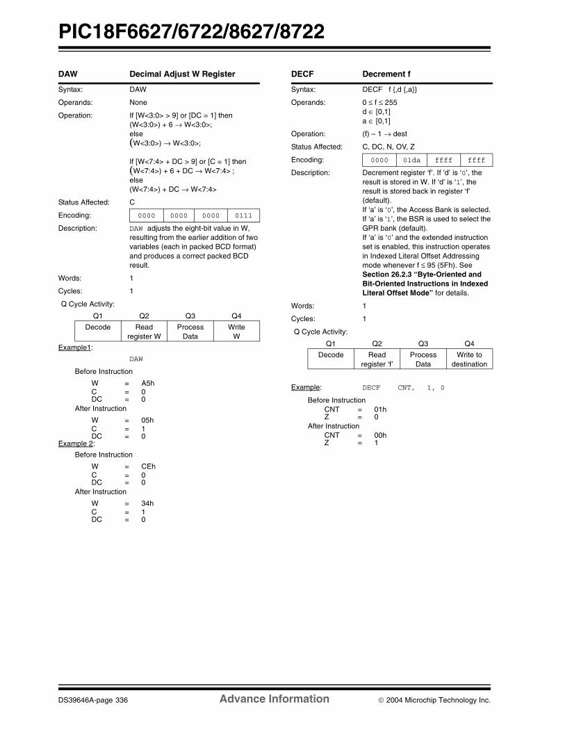
PIC18F6627/6722/8627/8722
DS39646A-page 336 Advance Information 2004 Microchip Technology Inc.
DAW Decimal Adjust W Register
Syntax: DAW
Operands: None
Operation: If [W<3:0> > 9] or [DC = 1] then(W<3:0>) + 6 → W<3:0>;else (W<3:0>) → W<3:0>;
If [W<7:4> + DC > 9] or [C = 1] then(W<7:4>) + 6 + DC → W<7:4> ;else (W<7:4>) + DC → W<7:4>
Status Affected: C
Encoding: 0000 0000 0000 0111
Description: DAW adjusts the eight-bit value in W, resulting from the earlier addition of two variables (each in packed BCD format) and produces a correct packed BCD result.
Words: 1
Cycles: 1
Q Cycle Activity:
Q1 Q2 Q3 Q4
Decode Readregister W
Process Data
WriteW
Example1:
DAW
Before Instruction
W = A5hC = 0DC = 0
After Instruction
W = 05hC = 1DC = 0
Example 2:
Before Instruction
W = CEhC = 0DC = 0
After Instruction
W = 34hC = 1DC = 0
DECF Decrement f
Syntax: DECF f ,d ,a
Operands: 0 ≤ f ≤ 255d ∈ [0,1]a ∈ [0,1]
Operation: (f) – 1 → dest
Status Affected: C, DC, N, OV, Z
Encoding: 0000 01da ffff ffff
Description: Decrement register ‘f’. If ‘d’ is ‘0’, the result is stored in W. If ‘d’ is ‘1’, the result is stored back in register ‘f’ (default). If ‘a’ is ‘0’, the Access Bank is selected. If ‘a’ is ‘1’, the BSR is used to select the GPR bank (default). If ‘a’ is ‘0’ and the extended instruction set is enabled, this instruction operates in Indexed Literal Offset Addressing mode whenever f ≤ 95 (5Fh). See Section 26.2.3 “Byte-Oriented and Bit-Oriented Instructions in Indexed Literal Offset Mode” for details.
Words: 1
Cycles: 1
Q Cycle Activity:
Q1 Q2 Q3 Q4
Decode Readregister ‘f’
Process Data
Write to destination
Example: DECF CNT, 1, 0
Before InstructionCNT = 01hZ = 0
After InstructionCNT = 00hZ = 1
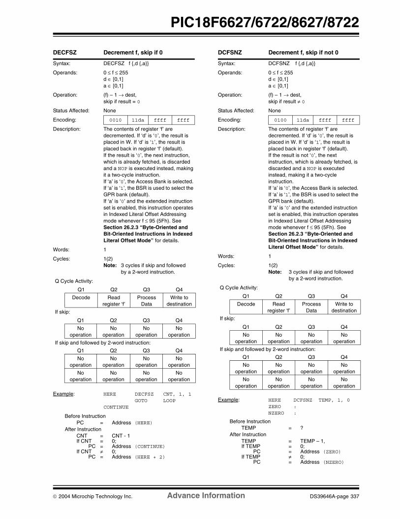
2004 Microchip Technology Inc. Advance Information DS39646A-page 337
PIC18F6627/6722/8627/8722
DECFSZ Decrement f, skip if 0
Syntax: DECFSZ f ,d ,a
Operands: 0 ≤ f ≤ 255d ∈ [0,1]a ∈ [0,1]
Operation: (f) – 1 → dest,skip if result = 0
Status Affected: None
Encoding: 0010 11da ffff ffff
Description: The contents of register ‘f’ are decremented. If ‘d’ is ‘0’, the result is placed in W. If ‘d’ is ‘1’, the result is placed back in register ‘f’ (default).If the result is ‘0’, the next instruction, which is already fetched, is discarded and a NOP is executed instead, making it a two-cycle instruction.If ‘a’ is ‘0’, the Access Bank is selected. If ‘a’ is ‘1’, the BSR is used to select the GPR bank (default). If ‘a’ is ‘0’ and the extended instruction set is enabled, this instruction operates in Indexed Literal Offset Addressing mode whenever f ≤ 95 (5Fh). See Section 26.2.3 “Byte-Oriented and Bit-Oriented Instructions in Indexed Literal Offset Mode” for details.
Words: 1
Cycles: 1(2)Note: 3 cycles if skip and followed
by a 2-word instruction.
Q Cycle Activity:
Q1 Q2 Q3 Q4
Decode Readregister ‘f’
Process Data
Write to destination
If skip:
Q1 Q2 Q3 Q4
No operation
No operation
No operation
No operation
If skip and followed by 2-word instruction:
Q1 Q2 Q3 Q4
No operation
No operation
No operation
No operation
No operation
No operation
No operation
No operation
Example: HERE DECFSZ CNT, 1, 1 GOTO LOOPCONTINUE
Before InstructionPC = Address (HERE)
After InstructionCNT = CNT - 1If CNT = 0;
PC = Address (CONTINUE)If CNT ≠ 0;
PC = Address (HERE + 2)
DCFSNZ Decrement f, skip if not 0
Syntax: DCFSNZ f ,d ,a
Operands: 0 ≤ f ≤ 255d ∈ [0,1]a ∈ [0,1]
Operation: (f) – 1 → dest,skip if result ≠ 0
Status Affected: None
Encoding: 0100 11da ffff ffff
Description: The contents of register ‘f’ are decremented. If ‘d’ is ‘0’, the result is placed in W. If ‘d’ is ‘1’, the result is placed back in register ‘f’ (default).If the result is not ‘0’, the next instruction, which is already fetched, is discarded and a NOP is executed instead, making it a two-cycle instruction. If ‘a’ is ‘0’, the Access Bank is selected. If ‘a’ is ‘1’, the BSR is used to select the GPR bank (default). If ‘a’ is ‘0’ and the extended instruction set is enabled, this instruction operates in Indexed Literal Offset Addressing mode whenever f ≤ 95 (5Fh). See Section 26.2.3 “Byte-Oriented and Bit-Oriented Instructions in Indexed Literal Offset Mode” for details.
Words: 1
Cycles: 1(2)Note: 3 cycles if skip and followed
by a 2-word instruction.
Q Cycle Activity:
Q1 Q2 Q3 Q4
Decode Readregister ‘f’
Process Data
Write to destination
If skip:
Q1 Q2 Q3 Q4
No operation
No operation
No operation
No operation
If skip and followed by 2-word instruction:
Q1 Q2 Q3 Q4
No operation
No operation
No operation
No operation
No operation
No operation
No operation
No operation
Example: HERE DCFSNZ TEMP, 1, 0ZERO : NZERO :
Before InstructionTEMP = ?
After InstructionTEMP = TEMP – 1,If TEMP = 0;
PC = Address (ZERO)If TEMP ≠ 0;
PC = Address (NZERO)

PIC18F6627/6722/8627/8722
DS39646A-page 338 Advance Information 2004 Microchip Technology Inc.
GOTO Unconditional Branch
Syntax: GOTO k
Operands: 0 ≤ k ≤ 1048575
Operation: k → PC<20:1>
Status Affected: None
Encoding:1st word (k<7:0>)2nd word(k<19:8>)
11101111
1111k19kkk
k7kkkkkkk
kkkk0kkkk8
Description: GOTO allows an unconditional branch anywhere within entire 2-Mbyte memory range. The 20-bit value ‘k’ is loaded into PC<20:1>. GOTO is always a two-cycle instruction.
Words: 2
Cycles: 2
Q Cycle Activity:
Q1 Q2 Q3 Q4
Decode Read literal ‘k’<7:0>,
No operation
Read literal ‘k’<19:8>,
Write to PC
No operation
No operation
No operation
No operation
Example: GOTO THERE
After InstructionPC = Address (THERE)
INCF Increment f
Syntax: INCF f ,d ,a
Operands: 0 ≤ f ≤ 255d ∈ [0,1]a ∈ [0,1]
Operation: (f) + 1 → dest
Status Affected: C, DC, N, OV, Z
Encoding: 0010 10da ffff ffff
Description: The contents of register ‘f’ are incremented. If ‘d’ is ‘0’, the result is placed in W. If ‘d’ is ‘1’, the result is placed back in register ‘f’ (default). If ‘a’ is ‘0’, the Access Bank is selected. If ‘a’ is ‘1’, the BSR is used to select the GPR bank (default). If ‘a’ is ‘0’ and the extended instruction set is enabled, this instruction operates in Indexed Literal Offset Addressing mode whenever f ≤ 95 (5Fh). See Section 26.2.3 “Byte-Oriented and Bit-Oriented Instructions in Indexed Literal Offset Mode” for details.
Words: 1
Cycles: 1
Q Cycle Activity:
Q1 Q2 Q3 Q4
Decode Readregister ‘f’
Process Data
Write to destination
Example: INCF CNT, 1, 0
Before InstructionCNT = FFhZ = 0C = ?DC = ?
After InstructionCNT = 00hZ = 1C = 1DC = 1

2004 Microchip Technology Inc. Advance Information DS39646A-page 339
PIC18F6627/6722/8627/8722
INCFSZ Increment f, skip if 0
Syntax: INCFSZ f ,d ,a
Operands: 0 ≤ f ≤ 255d ∈ [0,1]a ∈ [0,1]
Operation: (f) + 1 → dest,skip if result = 0
Status Affected: None
Encoding: 0011 11da ffff ffff
Description: The contents of register ‘f’ are incremented. If ‘d’ is ‘0’, the result is placed in W. If ‘d’ is ‘1’, the result is placed back in register ‘f’ (default).If the result is ‘0’, the next instruction, which is already fetched, is discarded and a NOP is executed instead, making it a two-cycle instruction. If ‘a’ is ‘0’, the Access Bank is selected. If ‘a’ is ‘1’, the BSR is used to select the GPR bank (default). If ‘a’ is ‘0’ and the extended instruction set is enabled, this instruction operates in Indexed Literal Offset Addressing mode whenever f ≤ 95 (5Fh). See Section 26.2.3 “Byte-Oriented and Bit-Oriented Instructions in Indexed Literal Offset Mode” for details.
Words: 1
Cycles: 1(2)Note: 3 cycles if skip and followed
by a 2-word instruction.
Q Cycle Activity:
Q1 Q2 Q3 Q4
Decode Readregister ‘f’
Process Data
Write to destination
If skip:
Q1 Q2 Q3 Q4
No operation
No operation
No operation
No operation
If skip and followed by 2-word instruction:
Q1 Q2 Q3 Q4
No operation
No operation
No operation
No operation
No operation
No operation
No operation
No operation
Example: HERE INCFSZ CNT, 1, 0NZERO : ZERO :
Before InstructionPC = Address (HERE)
After InstructionCNT = CNT + 1If CNT = 0;PC = Address (ZERO)If CNT ≠ 0;PC = Address (NZERO)
INFSNZ Increment f, skip if not 0
Syntax: INFSNZ f ,d ,a
Operands: 0 ≤ f ≤ 255d ∈ [0,1]a ∈ [0,1]
Operation: (f) + 1 → dest, skip if result ≠ 0
Status Affected: None
Encoding: 0100 10da ffff ffff
Description: The contents of register ‘f’ are incremented. If ‘d’ is ‘0’, the result is placed in W. If ‘d’ is ‘1’, the result is placed back in register ‘f’ (default).If the result is not ‘0’, the next instruction, which is already fetched, is discarded and a NOP is executed instead, making it a two-cycle instruction. If ‘a’ is ‘0’, the Access Bank is selected. If ‘a’ is ‘1’, the BSR is used to select the GPR bank (default). If ‘a’ is ‘0’ and the extended instruction set is enabled, this instruction operates in Indexed Literal Offset Addressing mode whenever f ≤ 95 (5Fh). See Section 26.2.3 “Byte-Oriented and Bit-Oriented Instructions in Indexed Literal Offset Mode” for details.
Words: 1
Cycles: 1(2)Note: 3 cycles if skip and followed
by a 2-word instruction.
Q Cycle Activity:
Q1 Q2 Q3 Q4
Decode Readregister ‘f’
Process Data
Write to destination
If skip:
Q1 Q2 Q3 Q4
No operation
No operation
No operation
No operation
If skip and followed by 2-word instruction:
Q1 Q2 Q3 Q4
No operation
No operation
No operation
No operation
No operation
No operation
No operation
No operation
Example: HERE INFSNZ REG, 1, 0ZERONZERO
Before InstructionPC = Address (HERE)
After InstructionREG = REG + 1If REG ≠ 0;PC = Address (NZERO)If REG = 0;PC = Address (ZERO)

PIC18F6627/6722/8627/8722
DS39646A-page 340 Advance Information 2004 Microchip Technology Inc.
IORLW Inclusive OR literal with W
Syntax: IORLW k
Operands: 0 ≤ k ≤ 255
Operation: (W) .OR. k → W
Status Affected: N, Z
Encoding: 0000 1001 kkkk kkkk
Description: The contents of W are ORed with the eight-bit literal ‘k’. The result is placed in W.
Words: 1
Cycles: 1
Q Cycle Activity:
Q1 Q2 Q3 Q4
Decode Read literal ‘k’
Process Data
Write to W
Example: IORLW 35h
Before Instruction
W = 9AhAfter Instruction
W = BFh
IORWF Inclusive OR W with f
Syntax: IORWF f ,d ,a
Operands: 0 ≤ f ≤ 255d ∈ [0,1]a ∈ [0,1]
Operation: (W) .OR. (f) → dest
Status Affected: N, Z
Encoding: 0001 00da ffff ffff
Description: Inclusive OR W with register ‘f’. If ‘d’ is ‘0’, the result is placed in W. If ‘d’ is ‘1’, the result is placed back in register ‘f’ (default). If ‘a’ is ‘0’, the Access Bank is selected. If ‘a’ is ‘1’, the BSR is used to select the GPR bank (default). If ‘a’ is ‘0’ and the extended instruction set is enabled, this instruction operates in Indexed Literal Offset Addressing mode whenever f ≤ 95 (5Fh). See Section 26.2.3 “Byte-Oriented and Bit-Oriented Instructions in Indexed Literal Offset Mode” for details.
Words: 1
Cycles: 1
Q Cycle Activity:
Q1 Q2 Q3 Q4
Decode Readregister ‘f’
Process Data
Write to destination
Example: IORWF RESULT, 0, 1
Before InstructionRESULT = 13hW = 91h
After InstructionRESULT = 13hW = 93h

2004 Microchip Technology Inc. Advance Information DS39646A-page 341
PIC18F6627/6722/8627/8722
LFSR Load FSR
Syntax: LFSR f, k
Operands: 0 ≤ f ≤ 20 ≤ k ≤ 4095
Operation: k → FSRf
Status Affected: None
Encoding: 11101111
11100000
00ffk7kkk
k11kkkkkkk
Description: The 12-bit literal ‘k’ is loaded into the File Select Register pointed to by ‘f’.
Words: 2
Cycles: 2
Q Cycle Activity:
Q1 Q2 Q3 Q4
Decode Read literal ‘k’ MSB
Process Data
Writeliteral ‘k’ MSB to FSRfH
Decode Read literal ‘k’ LSB
Process Data
Write literal ‘k’ to FSRfL
Example: LFSR 2, 3ABh
After InstructionFSR2H = 03hFSR2L = ABh
MOVF Move f
Syntax: MOVF f ,d ,a
Operands: 0 ≤ f ≤ 255d ∈ [0,1]a ∈ [0,1]
Operation: f → dest
Status Affected: N, Z
Encoding: 0101 00da ffff ffff
Description: The contents of register ‘f’ are moved to a destination dependent upon the status of ‘d’. If ‘d’ is ‘0’, the result is placed in W. If ‘d’ is ‘1’, the result is placed back in register ‘f’ (default). Location ‘f’ can be anywhere in the 256-byte bank.If ‘a’ is ‘0’, the Access Bank is selected. If ‘a’ is ‘1’, the BSR is used to select the GPR bank (default). If ‘a’ is ‘0’ and the extended instruction set is enabled, this instruction operates in Indexed Literal Offset Addressing mode whenever f ≤ 95 (5Fh). See Section 26.2.3 “Byte-Oriented and Bit-Oriented Instructions in Indexed Literal Offset Mode” for details.
Words: 1
Cycles: 1
Q Cycle Activity:
Q1 Q2 Q3 Q4
Decode Readregister ‘f’
Process Data
Write W
Example: MOVF REG, 0, 0
Before InstructionREG = 22hW = FFh
After InstructionREG = 22hW = 22h
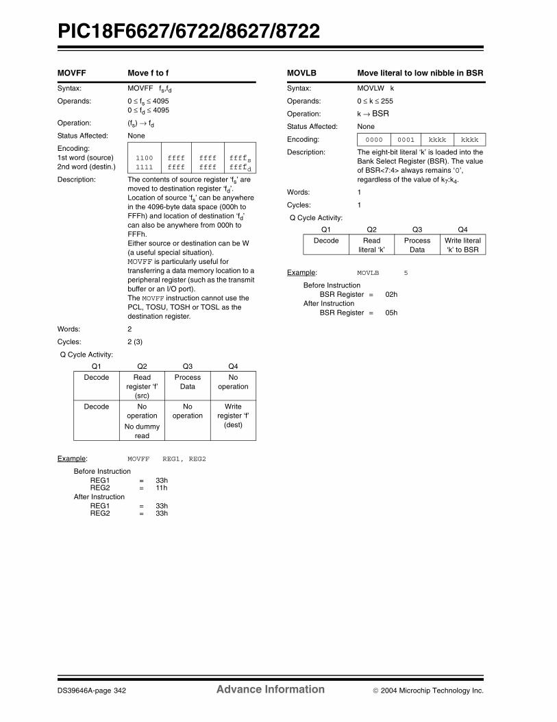
PIC18F6627/6722/8627/8722
DS39646A-page 342 Advance Information 2004 Microchip Technology Inc.
MOVFF Move f to f
Syntax: MOVFF fs,fd
Operands: 0 ≤ fs ≤ 40950 ≤ fd ≤ 4095
Operation: (fs) → fd
Status Affected: None
Encoding:1st word (source)2nd word (destin.)
11001111
ffffffff
ffffffff
ffffsffffd
Description: The contents of source register ‘fs’ are moved to destination register ‘fd’. Location of source ‘fs’ can be anywhere in the 4096-byte data space (000h to FFFh) and location of destination ‘fd’ can also be anywhere from 000h to FFFh.Either source or destination can be W (a useful special situation).MOVFF is particularly useful for transferring a data memory location to a peripheral register (such as the transmit buffer or an I/O port).The MOVFF instruction cannot use the PCL, TOSU, TOSH or TOSL as the destination register.
Words: 2
Cycles: 2 (3)
Q Cycle Activity:
Q1 Q2 Q3 Q4
Decode Readregister ‘f’
(src)
Process Data
No operation
Decode No operation
No dummy read
No operation
Write register ‘f’
(dest)
Example: MOVFF REG1, REG2
Before InstructionREG1 = 33hREG2 = 11h
After InstructionREG1 = 33hREG2 = 33h
MOVLB Move literal to low nibble in BSR
Syntax: MOVLW k
Operands: 0 ≤ k ≤ 255
Operation: k → BSR
Status Affected: None
Encoding: 0000 0001 kkkk kkkk
Description: The eight-bit literal ‘k’ is loaded into the Bank Select Register (BSR). The value of BSR<7:4> always remains ‘0’, regardless of the value of k7:k4.
Words: 1
Cycles: 1
Q Cycle Activity:
Q1 Q2 Q3 Q4
Decode Readliteral ‘k’
Process Data
Write literal ‘k’ to BSR
Example: MOVLB 5
Before InstructionBSR Register = 02h
After InstructionBSR Register = 05h

2004 Microchip Technology Inc. Advance Information DS39646A-page 343
PIC18F6627/6722/8627/8722
MOVLW Move literal to W
Syntax: MOVLW k
Operands: 0 ≤ k ≤ 255
Operation: k → W
Status Affected: None
Encoding: 0000 1110 kkkk kkkk
Description: The eight-bit literal ‘k’ is loaded into W.
Words: 1
Cycles: 1
Q Cycle Activity:
Q1 Q2 Q3 Q4
Decode Readliteral ‘k’
Process Data
Write to W
Example: MOVLW 5Ah
After Instruction
W = 5Ah
MOVWF Move W to f
Syntax: MOVWF f ,a
Operands: 0 ≤ f ≤ 255a ∈ [0,1]
Operation: (W) → f
Status Affected: None
Encoding: 0110 111a ffff ffff
Description: Move data from W to register ‘f’. Location ‘f’ can be anywhere in the 256-byte bank. If ‘a’ is ‘0’, the Access Bank is selected. If ‘a’ is ‘1’, the BSR is used to select the GPR bank (default). If ‘a’ is ‘0’ and the extended instruction set is enabled, this instruction operates in Indexed Literal Offset Addressing mode whenever f ≤ 95 (5Fh). See Section 26.2.3 “Byte-Oriented and Bit-Oriented Instructions in Indexed Literal Offset Mode” for details.
Words: 1
Cycles: 1
Q Cycle Activity:
Q1 Q2 Q3 Q4
Decode Readregister ‘f’
Process Data
Writeregister ‘f’
Example: MOVWF REG, 0
Before Instruction
W = 4FhREG = FFh
After Instruction
W = 4FhREG = 4Fh

PIC18F6627/6722/8627/8722
DS39646A-page 344 Advance Information 2004 Microchip Technology Inc.
MULLW Multiply literal with W
Syntax: MULLW k
Operands: 0 ≤ k ≤ 255
Operation: (W) x k → PRODH:PRODL
Status Affected: None
Encoding: 0000 1101 kkkk kkkk
Description: An unsigned multiplication is carried out between the contents of W and the 8-bit literal ‘k’. The 16-bit result is placed in the PRODH:PRODL register pair. PRODH contains the high byte.W is unchanged.None of the Status flags are affected.Note that neither overflow nor carry is possible in this operation. A zero result is possible but not detected.
Words: 1
Cycles: 1
Q Cycle Activity:
Q1 Q2 Q3 Q4
Decode Read literal ‘k’
Process Data
Write registers PRODH:PRODL
Example: MULLW 0C4h
Before Instruction
W = E2hPRODH = ?PRODL = ?
After Instruction
W = E2hPRODH = ADhPRODL = 08h
MULWF Multiply W with f
Syntax: MULWF f ,a
Operands: 0 ≤ f ≤ 255a ∈ [0,1]
Operation: (W) x (f) → PRODH:PRODL
Status Affected: None
Encoding: 0000 001a ffff ffff
Description: An unsigned multiplication is carried out between the contents of W and the register file location ‘f’. The 16-bit result is stored in the PRODH:PRODL register pair. PRODH contains the high byte. Both W and ‘f’ are unchanged.None of the Status flags are affected.Note that neither overflow nor carry is possible in this operation. A zero result is possible but not detected.If ‘a’ is ‘0’, the Access Bank is selected. If ‘a’ is ‘1’, the BSR is used to select the GPR bank (default). If ‘a’ is ‘0’ and the extended instruction set is enabled, this instruction operates in Indexed Literal Offset Addressing mode whenever f ≤ 95 (5Fh). See Section 26.2.3 “Byte-Oriented and Bit-Oriented Instructions in Indexed Literal Offset Mode” for details.
Words: 1
Cycles: 1
Q Cycle Activity:
Q1 Q2 Q3 Q4
Decode Readregister ‘f’
Process Data
Writeregisters PRODH:PRODL
Example: MULWF REG, 1
Before Instruction
W = C4hREG = B5hPRODH = ?PRODL = ?
After Instruction
W = C4hREG = B5hPRODH = 8AhPRODL = 94h

2004 Microchip Technology Inc. Advance Information DS39646A-page 345
PIC18F6627/6722/8627/8722
NEGF Negate f
Syntax: NEGF f ,a
Operands: 0 ≤ f ≤ 255a ∈ [0,1]
Operation: ( f ) + 1 → f
Status Affected: N, OV, C, DC, Z
Encoding: 0110 110a ffff ffff
Description: Location ‘f’ is negated using 2’s complement. The result is placed in the data memory location ‘f’. If ‘a’ is ‘0’, the Access Bank is selected. If ‘a’ is ‘1’, the BSR is used to select the GPR bank (default). If ‘a’ is ‘0’ and the extended instruction set is enabled, this instruction operates in Indexed Literal Offset Addressing mode whenever f ≤ 95 (5Fh). See Section 26.2.3 “Byte-Oriented and Bit-Oriented Instructions in Indexed Literal Offset Mode” for details.
Words: 1
Cycles: 1
Q Cycle Activity:
Q1 Q2 Q3 Q4
Decode Readregister ‘f’
Process Data
Write register ‘f’
Example: NEGF REG, 1
Before InstructionREG = 0011 1010 [3Ah]
After InstructionREG = 1100 0110 [C6h]
NOP No Operation
Syntax: NOP
Operands: None
Operation: No operation
Status Affected: None
Encoding: 00001111
0000xxxx
0000xxxx
0000xxxx
Description: No operation.
Words: 1
Cycles: 1
Q Cycle Activity:
Q1 Q2 Q3 Q4
Decode No operation
No operation
No operation
Example:
None.

PIC18F6627/6722/8627/8722
DS39646A-page 346 Advance Information 2004 Microchip Technology Inc.
POP Pop Top of Return Stack
Syntax: POP
Operands: None
Operation: (TOS) → bit bucket
Status Affected: None
Encoding: 0000 0000 0000 0110
Description: The TOS value is pulled off the return stack and is discarded. The TOS value then becomes the previous value that was pushed onto the return stack.This instruction is provided to enable the user to properly manage the return stack to incorporate a software stack.
Words: 1
Cycles: 1
Q Cycle Activity:
Q1 Q2 Q3 Q4
Decode Nooperation
POP TOS value
Nooperation
Example: POPGOTO NEW
Before InstructionTOS = 0031A2hStack (1 level down) = 014332h
After InstructionTOS = 014332hPC = NEW
PUSH Push Top of Return Stack
Syntax: PUSH
Operands: None
Operation: (PC + 2) → TOS
Status Affected: None
Encoding: 0000 0000 0000 0101
Description: The PC + 2 is pushed onto the top of the return stack. The previous TOS value is pushed down on the stack.This instruction allows implementing a software stack by modifying TOS and then pushing it onto the return stack.
Words: 1
Cycles: 1
Q Cycle Activity:
Q1 Q2 Q3 Q4
Decode PUSH PC + 2 onto return stack
No operation
No operation
Example: PUSH
Before InstructionTOS = 345AhPC = 0124h
After InstructionPC = 0126hTOS = 0126hStack (1 level down) = 345Ah

2004 Microchip Technology Inc. Advance Information DS39646A-page 347
PIC18F6627/6722/8627/8722
RCALL Relative Call
Syntax: RCALL n
Operands: -1024 ≤ n ≤ 1023
Operation: (PC) + 2 → TOS,(PC) + 2 + 2n → PC
Status Affected: None
Encoding: 1101 1nnn nnnn nnnn
Description: Subroutine call with a jump up to 1K from the current location. First, return address (PC + 2) is pushed onto the stack. Then, add the 2’s complement number ‘2n’ to the PC. Since the PC will have incremented to fetch the next instruction, the new address will be PC + 2 + 2n. This instruction is a two-cycle instruction.
Words: 1
Cycles: 2
Q Cycle Activity:
Q1 Q2 Q3 Q4
Decode Read literal ‘n’
PUSH PC to stack
Process Data
Write to PC
No operation
No operation
No operation
No operation
Example: HERE RCALL Jump
Before InstructionPC = Address (HERE)
After InstructionPC = Address (Jump)TOS = Address (HERE + 2)
RESET Reset
Syntax: RESET
Operands: None
Operation: Reset all registers and flags that are affected by a MCLR Reset.
Status Affected: All
Encoding: 0000 0000 1111 1111
Description: This instruction provides a way to execute a MCLR Reset in software.
Words: 1
Cycles: 1
Q Cycle Activity:
Q1 Q2 Q3 Q4
Decode Start Reset
No operation
No operation
Example: RESET
After InstructionRegisters = Reset ValueFlags* = Reset Value
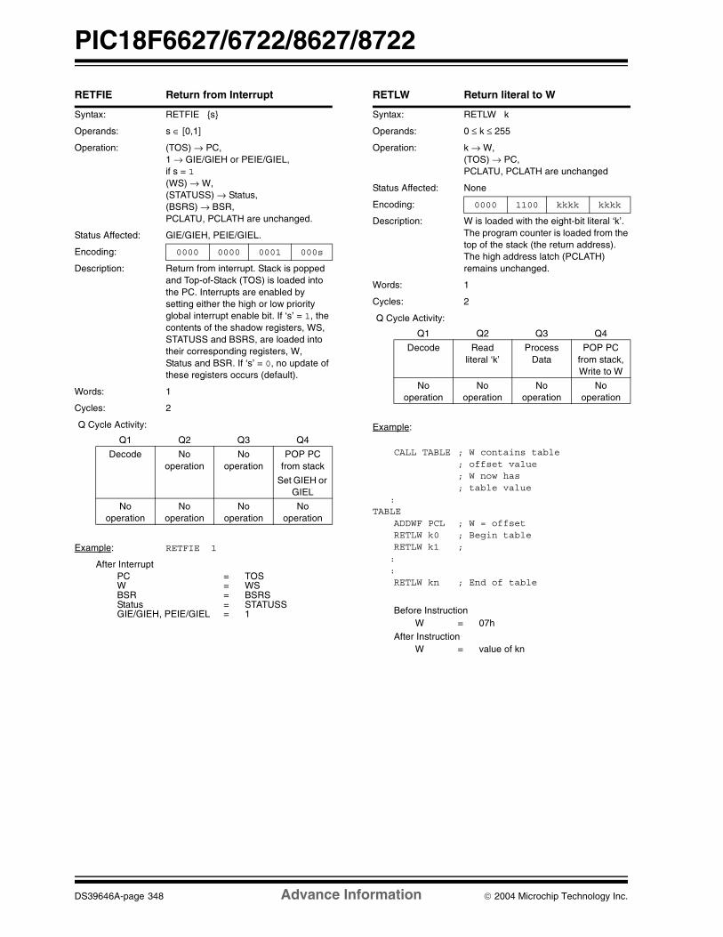
PIC18F6627/6722/8627/8722
DS39646A-page 348 Advance Information 2004 Microchip Technology Inc.
RETFIE Return from Interrupt
Syntax: RETFIE s
Operands: s ∈ [0,1]
Operation: (TOS) → PC,1 → GIE/GIEH or PEIE/GIEL,if s = 1(WS) → W,(STATUSS) → Status,(BSRS) → BSR,PCLATU, PCLATH are unchanged.
Status Affected: GIE/GIEH, PEIE/GIEL.
Encoding: 0000 0000 0001 000s
Description: Return from interrupt. Stack is popped and Top-of-Stack (TOS) is loaded into the PC. Interrupts are enabled by setting either the high or low priority global interrupt enable bit. If ‘s’ = 1, the contents of the shadow registers, WS, STATUSS and BSRS, are loaded into their corresponding registers, W, Status and BSR. If ‘s’ = 0, no update of these registers occurs (default).
Words: 1
Cycles: 2
Q Cycle Activity:
Q1 Q2 Q3 Q4
Decode No operation
No operation
POP PC from stack
Set GIEH or GIEL
No operation
No operation
No operation
No operation
Example: RETFIE 1
After InterruptPC = TOSW = WSBSR = BSRSStatus = STATUSSGIE/GIEH, PEIE/GIEL = 1
RETLW Return literal to W
Syntax: RETLW k
Operands: 0 ≤ k ≤ 255
Operation: k → W,(TOS) → PC,PCLATU, PCLATH are unchanged
Status Affected: None
Encoding: 0000 1100 kkkk kkkk
Description: W is loaded with the eight-bit literal ‘k’. The program counter is loaded from the top of the stack (the return address). The high address latch (PCLATH) remains unchanged.
Words: 1
Cycles: 2
Q Cycle Activity:
Q1 Q2 Q3 Q4
Decode Readliteral ‘k’
Process Data
POP PC from stack, Write to W
No operation
No operation
No operation
No operation
Example:
CALL TABLE ; W contains table ; offset value ; W now has ; table value :TABLE
ADDWF PCL ; W = offsetRETLW k0 ; Begin tableRETLW k1 ;
: :
RETLW kn ; End of table
Before InstructionW = 07h
After InstructionW = value of kn

2004 Microchip Technology Inc. Advance Information DS39646A-page 349
PIC18F6627/6722/8627/8722
RETURN Return from Subroutine
Syntax: RETURN s
Operands: s ∈ [0,1]
Operation: (TOS) → PC,if s = 1(WS) → W,(STATUSS) → Status,(BSRS) → BSR,PCLATU, PCLATH are unchanged
Status Affected: None
Encoding: 0000 0000 0001 001s
Description: Return from subroutine. The stack is popped and the top of the stack (TOS) is loaded into the program counter. If ‘s’= 1, the contents of the shadow registers, WS, STATUSS and BSRS, are loaded into their corresponding registers, W, Status and BSR. If ‘s’ = 0, no update of these registers occurs (default).
Words: 1
Cycles: 2
Q Cycle Activity:
Q1 Q2 Q3 Q4
Decode No operation
Process Data
POP PC from stack
No operation
No operation
No operation
No operation
Example: RETURN
After Instruction:PC = TOS
RLCF Rotate Left f through Carry
Syntax: RLCF f ,d ,a
Operands: 0 ≤ f ≤ 255d ∈ [0,1]a ∈ [0,1]
Operation: (f<n>) → dest<n + 1>,(f<7>) → C,(C) → dest<0>
Status Affected: C, N, Z
Encoding: 0011 01da ffff ffff
Description: The contents of register ‘f’ are rotated one bit to the left through the CARRY flag. If ‘d’ is ‘0’, the result is placed in W. If ‘d’ is ‘1’, the result is stored back in register ‘f’ (default). If ‘a’ is ‘0’, the Access Bank is selected. If ‘a’ is ‘1’, the BSR is used to select the GPR bank (default). If ‘a’ is ‘0’ and the extended instruction set is enabled, this instruction operates in Indexed Literal Offset Addressing mode whenever f ≤ 95 (5Fh). See Section 26.2.3 “Byte-Oriented and Bit-Oriented Instructions in Indexed Literal Offset Mode” for details.
Words: 1
Cycles: 1
Q Cycle Activity:
Q1 Q2 Q3 Q4
Decode Readregister ‘f’
Process Data
Write to destination
Example: RLCF REG, 0, 0
Before InstructionREG = 1110 0110C = 0
After InstructionREG = 1110 0110
W = 1100 1100C = 1
C register f

PIC18F6627/6722/8627/8722
DS39646A-page 350 Advance Information 2004 Microchip Technology Inc.
RLNCF Rotate Left f (No Carry)
Syntax: RLNCF f ,d ,a
Operands: 0 ≤ f ≤ 255d ∈ [0,1]a ∈ [0,1]
Operation: (f<n>) → dest<n + 1>,(f<7>) → dest<0>
Status Affected: N, Z
Encoding: 0100 01da ffff ffff
Description: The contents of register ‘f’ are rotated one bit to the left. If ‘d’ is ‘0’, the result is placed in W. If ‘d’ is ‘1’, the result is stored back in register ‘f’ (default).If ‘a’ is ‘0’, the Access Bank is selected. If ‘a’ is ‘1’, the BSR is used to select the GPR bank (default). If ‘a’ is ‘0’ and the extended instruction set is enabled, this instruction operates in Indexed Literal Offset Addressing mode whenever f ≤ 95 (5Fh). See Section 26.2.3 “Byte-Oriented and Bit-Oriented Instructions in Indexed Literal Offset Mode” for details.
Words: 1
Cycles: 1
Q Cycle Activity:
Q1 Q2 Q3 Q4
Decode Readregister ‘f’
Process Data
Write to destination
Example: RLNCF REG, 1, 0
Before InstructionREG = 1010 1011
After InstructionREG = 0101 0111
register f
RRCF Rotate Right f through Carry
Syntax: RRCF f ,d ,a
Operands: 0 ≤ f ≤ 255d ∈ [0,1]a ∈ [0,1]
Operation: (f<n>) → dest<n – 1>,(f<0>) → C,(C) → dest<7>
Status Affected: C, N, Z
Encoding: 0011 00da ffff ffff
Description: The contents of register ‘f’ are rotated one bit to the right through the CARRY flag. If ‘d’ is ‘0’, the result is placed in W. If ‘d’ is ‘1’, the result is placed back in register ‘f’ (default). If ‘a’ is ‘0’, the Access Bank is selected. If ‘a’ is ‘1’, the BSR is used to select the GPR bank (default). If ‘a’ is ‘0’ and the extended instruction set is enabled, this instruction operates in Indexed Literal Offset Addressing mode whenever f ≤ 95 (5Fh). See Section 26.2.3 “Byte-Oriented and Bit-Oriented Instructions in Indexed Literal Offset Mode” for details.
Words: 1
Cycles: 1
Q Cycle Activity:
Q1 Q2 Q3 Q4
Decode Readregister ‘f’
Process Data
Write to destination
Example: RRCF REG, 0, 0
Before InstructionREG = 1110 0110C = 0
After InstructionREG = 1110 0110
W = 0111 0011C = 0
C register f

2004 Microchip Technology Inc. Advance Information DS39646A-page 351
PIC18F6627/6722/8627/8722
RRNCF Rotate Right f (No Carry)
Syntax: RRNCF f ,d ,a
Operands: 0 ≤ f ≤ 255d ∈ [0,1]a ∈ [0,1]
Operation: (f<n>) → dest<n – 1>,(f<0>) → dest<7>
Status Affected: N, Z
Encoding: 0100 00da ffff ffff
Description: The contents of register ‘f’ are rotated one bit to the right. If ‘d’ is ‘0’, the result is placed in W. If ‘d’ is ‘1’, the result is placed back in register ‘f’ (default).If ‘a’ is ‘0’, the Access Bank will be selected, overriding the BSR value. If ‘a’ is ‘1’, then the bank will be selected as per the BSR value (default).If ‘a’ is ‘0’ and the extended instruction set is enabled, this instruction operates in Indexed Literal Offset Addressing mode whenever f ≤ 95 (5Fh). See Section 26.2.3 “Byte-Oriented and Bit-Oriented Instructions in Indexed Literal Offset Mode” for details.
Words: 1
Cycles: 1
Q Cycle Activity:
Q1 Q2 Q3 Q4
Decode Readregister ‘f’
Process Data
Write to destination
Example 1: RRNCF REG, 1, 0
Before InstructionREG = 1101 0111
After InstructionREG = 1110 1011
Example 2: RRNCF REG, 0, 0
Before Instruction
W = ?REG = 1101 0111
After Instruction
W = 1110 1011REG = 1101 0111
register f
SETF Set f
Syntax: SETF f ,a
Operands: 0 ≤ f ≤ 255a ∈ [0,1]
Operation: FFh → f
Status Affected: None
Encoding: 0110 100a ffff ffff
Description: The contents of the specified register are set to FFh. If ‘a’ is ‘0’, the Access Bank is selected. If ‘a’ is ‘1’, the BSR is used to select the GPR bank (default). If ‘a’ is ‘0’ and the extended instruction set is enabled, this instruction operates in Indexed Literal Offset Addressing mode whenever f ≤ 95 (5Fh). See Section 26.2.3 “Byte-Oriented and Bit-Oriented Instructions in Indexed Literal Offset Mode” for details.
Words: 1
Cycles: 1
Q Cycle Activity:
Q1 Q2 Q3 Q4
Decode Readregister ‘f’
Process Data
Writeregister ‘f’
Example: SETF REG, 1
Before InstructionREG = 5Ah
After InstructionREG = FFh

PIC18F6627/6722/8627/8722
DS39646A-page 352 Advance Information 2004 Microchip Technology Inc.
SLEEP Enter Sleep mode
Syntax: SLEEP
Operands: None
Operation: 00h → WDT,0 → WDT postscaler,1 → TO,0 → PD
Status Affected: TO, PD
Encoding: 0000 0000 0000 0011
Description: The Power-down status bit (PD) is cleared. The Time-out status bit (TO) is set. Watchdog Timer and its postscaler are cleared.The processor is put into Sleep mode with the oscillator stopped.
Words: 1
Cycles: 1
Q Cycle Activity:
Q1 Q2 Q3 Q4
Decode No operation
Process Data
Go toSleep
Example: SLEEP
Before InstructionTO = ?PD = ?
After InstructionTO = 1 †PD = 0
† If WDT causes wake-up, this bit is cleared.
SUBFWB Subtract f from W with borrow
Syntax: SUBFWB f ,d ,a
Operands: 0 ≤ f ≤ 255d ∈ [0,1]a ∈ [0,1]
Operation: (W) – (f) – (C) → dest
Status Affected: N, OV, C, DC, Z
Encoding: 0101 01da ffff ffff
Description: Subtract register ‘f’ and CARRY flag (borrow) from W (2’s complement method). If ‘d’ is ‘0’, the result is stored in W. If ‘d’ is ‘1’, the result is stored in register ‘f’ (default). If ‘a’ is ‘0’, the Access Bank is selected. If ‘a’ is ‘1’, the BSR is used to select the GPR bank (default). If ‘a’ is ‘0’ and the extended instruction set is enabled, this instruction operates in Indexed Literal Offset Addressing mode whenever f ≤ 95 (5Fh). See Section 26.2.3 “Byte-Oriented and Bit-Oriented Instructions in Indexed Literal Offset Mode” for details.
Words: 1
Cycles: 1
Q Cycle Activity:
Q1 Q2 Q3 Q4
Decode Readregister ‘f’
Process Data
Write to destination
Example 1: SUBFWB REG, 1, 0
Before InstructionREG = 3W = 2C = 1
After InstructionREG = FFW = 2C = 0Z = 0N = 1 ; result is negative
Example 2: SUBFWB REG, 0, 0
Before InstructionREG = 2W = 5C = 1
After InstructionREG = 2W = 3C = 1Z = 0N = 0 ; result is positive
Example 3: SUBFWB REG, 1, 0
Before InstructionREG = 1W = 2C = 0
After InstructionREG = 0W = 2C = 1Z = 1 ; result is zeroN = 0
2004 Microchip Technology Inc. Advance Information DS39646A-page 353
PIC18F6627/6722/8627/8722
SUBLW Subtract W from literal
Syntax: SUBLW k
Operands: 0 ≤ k ≤ 255
Operation: k – (W) → W
Status Affected: N, OV, C, DC, Z
Encoding: 0000 1000 kkkk kkkk
Description W is subtracted from the eight-bit literal ‘k’. The result is placed in W.
Words: 1
Cycles: 1
Q Cycle Activity:
Q1 Q2 Q3 Q4
Decode Readliteral ‘k’
Process Data
Write to W
Example 1: SUBLW 02h
Before InstructionW = 01hC = ?
After InstructionW = 01hC = 1 ; result is positiveZ = 0N = 0
Example 2: SUBLW 02h
Before InstructionW = 02hC = ?
After InstructionW = 00hC = 1 ; result is zeroZ = 1N = 0
Example 3: SUBLW 02h
Before InstructionW = 03hC = ?
After InstructionW = FFh ; (2’s complement)C = 0 ; result is negativeZ = 0N = 1
SUBWF Subtract W from f
Syntax: SUBWF f ,d ,a
Operands: 0 ≤ f ≤ 255d ∈ [0,1]a ∈ [0,1]
Operation: (f) – (W) → dest
Status Affected: N, OV, C, DC, Z
Encoding: 0101 11da ffff ffff
Description: Subtract W from register ‘f’ (2’s complement method). If ‘d’ is ‘0’, the result is stored in W. If ‘d’ is ‘1’, the result is stored back in register ‘f’ (default). If ‘a’ is ‘0’, the Access Bank is selected. If ‘a’ is ‘1’, the BSR is used to select the GPR bank (default). If ‘a’ is ‘0’ and the extended instruction set is enabled, this instruction operates in Indexed Literal Offset Addressing mode whenever f ≤ 95 (5Fh). See Section 26.2.3 “Byte-Oriented and Bit-Oriented Instructions in Indexed Literal Offset Mode” for details.
Words: 1
Cycles: 1
Q Cycle Activity:
Q1 Q2 Q3 Q4
Decode Readregister ‘f’
Process Data
Write to destination
Example 1: SUBWF REG, 1, 0
Before InstructionREG = 3W = 2C = ?
After InstructionREG = 1W = 2C = 1 ; result is positiveZ = 0N = 0
Example 2: SUBWF REG, 0, 0
Before InstructionREG = 2W = 2C = ?
After InstructionREG = 2W = 0C = 1 ; result is zeroZ = 1N = 0
Example 3: SUBWF REG, 1, 0
Before InstructionREG = 1W = 2C = ?
After InstructionREG = FFh ;(2’s complement)W = 2C = 0 ; result is negativeZ = 0N = 1

PIC18F6627/6722/8627/8722
DS39646A-page 354 Advance Information 2004 Microchip Technology Inc.
SUBWFB Subtract W from f with Borrow
Syntax: SUBWFB f ,d ,a
Operands: 0 ≤ f ≤ 255d ∈ [0,1]a ∈ [0,1]
Operation: (f) – (W) – (C) → dest
Status Affected: N, OV, C, DC, Z
Encoding: 0101 10da ffff ffff
Description: Subtract W and the CARRY flag (borrow) from register ‘f’ (2’s comple-ment method). If ‘d’ is ‘0’, the result is stored in W. If ‘d’ is ‘1’, the result is stored back in register ‘f’ (default).If ‘a’ is ‘0’, the Access Bank is selected. If ‘a’ is ‘1’, the BSR is used to select the GPR bank (default). If ‘a’ is ‘0’ and the extended instruction set is enabled, this instruction operates in Indexed Literal Offset Addressing mode whenever f ≤ 95 (5Fh). See Section 26.2.3 “Byte-Oriented and Bit-Oriented Instructions in Indexed Literal Offset Mode” for details.
Words: 1
Cycles: 1
Q Cycle Activity:
Q1 Q2 Q3 Q4Decode Read
register ‘f’Process
DataWrite to
destination
Example 1: SUBWFB REG, 1, 0
Before InstructionREG = 19h (0001 1001)W = 0Dh (0000 1101)C = 1
After InstructionREG = 0Ch (0000 1011)W = 0Dh (0000 1101)C = 1Z = 0N = 0 ; result is positive
Example 2: SUBWFB REG, 0, 0
Before InstructionREG = 1Bh (0001 1011)W = 1Ah (0001 1010)C = 0
After InstructionREG = 1Bh (0001 1011)W = 00hC = 1Z = 1 ; result is zeroN = 0
Example 3: SUBWFB REG, 1, 0
Before InstructionREG = 03h (0000 0011)W = 0Eh (0000 1101)C = 1
After InstructionREG = F5h (1111 0100)
; [2’s comp]W = 0Eh (0000 1101)C = 0Z = 0N = 1 ; result is negative
SWAPF Swap f
Syntax: SWAPF f ,d ,a
Operands: 0 ≤ f ≤ 255d ∈ [0,1]a ∈ [0,1]
Operation: (f<3:0>) → dest<7:4>,(f<7:4>) → dest<3:0>
Status Affected: None
Encoding: 0011 10da ffff ffff
Description: The upper and lower nibbles of register ‘f’ are exchanged. If ‘d’ is ‘0’, the result is placed in W. If ‘d’ is ‘1’, the result is placed in register ‘f’ (default).If ‘a’ is ‘0’, the Access Bank is selected. If ‘a’ is ‘1’, the BSR is used to select the GPR bank (default). If ‘a’ is ‘0’ and the extended instruction set is enabled, this instruction operates in Indexed Literal Offset Addressing mode whenever f ≤ 95 (5Fh). See Section 26.2.3 “Byte-Oriented and Bit-Oriented Instructions in Indexed Literal Offset Mode” for details.
Words: 1
Cycles: 1
Q Cycle Activity:
Q1 Q2 Q3 Q4
Decode Readregister ‘f’
Process Data
Write to destination
Example: SWAPF REG, 1, 0
Before InstructionREG = 53h
After InstructionREG = 35h

2004 Microchip Technology Inc. Advance Information DS39646A-page 355
PIC18F6627/6722/8627/8722
TBLRD Table Read
Syntax: TBLRD ( *; *+; *-; +*)
Operands: None
Operation: if TBLRD *,(Prog Mem (TBLPTR)) → TABLAT;TBLPTR – No Change;if TBLRD *+,(Prog Mem (TBLPTR)) → TABLAT;(TBLPTR) + 1 → TBLPTR;if TBLRD *-,(Prog Mem (TBLPTR)) → TABLAT;(TBLPTR) – 1 → TBLPTR;if TBLRD +*,(TBLPTR) + 1 → TBLPTR;(Prog Mem (TBLPTR)) → TABLAT;
Status Affected: None
Encoding: 0000 0000 0000 10nn nn=0 * =1 *+ =2 *- =3 +*
Description: This instruction is used to read the contents of Program Memory (P.M.). To address the program memory, a pointer called Table Pointer (TBLPTR) is used.The TBLPTR (a 21-bit pointer) points to each byte in the program memory. TBLPTR has a 2-Mbyte address range.
TBLPTR[0] = 0: Least Significant Byte of Program Memory Word
TBLPTR[0] = 1: Most Significant Byte of Program Memory Word
The TBLRD instruction can modify the value of TBLPTR as follows:• no change• post-increment• post-decrement• pre-increment
Words: 1
Cycles: 2
Q Cycle Activity:
Q1 Q2 Q3 Q4
Decode No operation
No operation
No operation
No operation
No operation(Read Program
Memory)
No operation
No operation(Write TABLAT)
TBLRD Table Read (Continued)
Example1: TBLRD *+ ;
Before InstructionTABLAT = 55hTBLPTR = 00A356hMEMORY (00A356h) = 34h
After InstructionTABLAT = 34hTBLPTR = 00A357h
Example2: TBLRD +* ;
Before InstructionTABLAT = AAhTBLPTR = 01A357hMEMORY (01A357h) = 12hMEMORY (01A358h) = 34h
After InstructionTABLAT = 34hTBLPTR = 01A358h

PIC18F6627/6722/8627/8722
DS39646A-page 356 Advance Information 2004 Microchip Technology Inc.
TBLWT Table Write
Syntax: TBLWT ( *; *+; *-; +*)
Operands: None
Operation: if TBLWT*,(TABLAT) → Holding Register;TBLPTR – No Change;if TBLWT*+,(TABLAT) → Holding Register;(TBLPTR) + 1 → TBLPTR;if TBLWT*-,(TABLAT) → Holding Register;(TBLPTR) – 1 → TBLPTR;if TBLWT+*,(TBLPTR) + 1 → TBLPTR;(TABLAT) → Holding Register;
Status Affected: None
Encoding: 0000 0000 0000 11nnnn=0 * =1 *+ =2 *- =3 +*
Description: This instruction uses the 3 LSBs of TBLPTR to determine which of the 8 holding registers the TABLAT is written to. The holding registers are used to program the contents of Program Memory (P.M.). (Refer to Section 6.0 “Flash Program Memory” for additional details on programming Flash memory.)The TBLPTR (a 21-bit pointer) points to each byte in the program memory. TBLPTR has a 2-MByte address range. The LSb of the TBLPTR selects which byte of the program memory location to access.
TBLPTR[0] = 0: Least Significant Byte of Program Memory Word
TBLPTR[0] = 1: Most Significant Byte of Program Memory Word
The TBLWT instruction can modify the value of TBLPTR as follows:• no change• post-increment• post-decrement• pre-increment
Words: 1
Cycles: 2
Q Cycle Activity:
Q1 Q2 Q3 Q4
Decode No operation
No operation
No operation
No operation
No operation
(ReadTABLAT)
No operation
No operation(Write to Holding
Register )
TBLWT Table Write (Continued)
Example1: TBLWT *+;
Before InstructionTABLAT = 55hTBLPTR = 00A356hHOLDING REGISTER (00A356h) = FFh
After Instructions (table write completion)TABLAT = 55hTBLPTR = 00A357hHOLDING REGISTER (00A356h) = 55h
Example 2: TBLWT +*;
Before InstructionTABLAT = 34hTBLPTR = 01389AhHOLDING REGISTER (01389Ah) = FFhHOLDING REGISTER (01389Bh) = FFh
After Instruction (table write completion)TABLAT = 34hTBLPTR = 01389BhHOLDING REGISTER (01389Ah) = FFhHOLDING REGISTER (01389Bh) = 34h

2004 Microchip Technology Inc. Advance Information DS39646A-page 357
PIC18F6627/6722/8627/8722
TSTFSZ Test f, skip if 0
Syntax: TSTFSZ f ,a
Operands: 0 ≤ f ≤ 255a ∈ [0,1]
Operation: skip if f = 0
Status Affected: None
Encoding: 0110 011a ffff ffff
Description: If ‘f’ = 0, the next instruction fetched during the current instruction execution is discarded and a NOP is executed, making this a two-cycle instruction. If ‘a’ is ‘0’, the Access Bank is selected. If ‘a’ is ‘1’, the BSR is used to select the GPR bank (default). If ‘a’ is ‘0’ and the extended instruction set is enabled, this instruction operates in Indexed Literal Offset Addressing mode whenever f ≤ 95 (5Fh). See Section 26.2.3 “Byte-Oriented and Bit-Oriented Instructions in Indexed Literal Offset Mode” for details.
Words: 1
Cycles: 1(2)Note: 3 cycles if skip and followed
by a 2-word instruction.
Q Cycle Activity:
Q1 Q2 Q3 Q4
Decode Readregister ‘f’
Process Data
No operation
If skip:
Q1 Q2 Q3 Q4
No operation
No operation
No operation
No operation
If skip and followed by 2-word instruction:
Q1 Q2 Q3 Q4
No operation
No operation
No operation
No operation
No operation
No operation
No operation
No operation
Example: HERE TSTFSZ CNT, 1NZERO :ZERO :
Before InstructionPC = Address (HERE)
After InstructionIf CNT = 00h,PC = Address (ZERO)If CNT ≠ 00h,PC = Address (NZERO)
XORLW Exclusive OR literal with W
Syntax: XORLW k
Operands: 0 ≤ k ≤ 255
Operation: (W) .XOR. k → W
Status Affected: N, Z
Encoding: 0000 1010 kkkk kkkk
Description: The contents of W are XORed with the 8-bit literal ‘k’. The result is placed in W.
Words: 1
Cycles: 1
Q Cycle Activity:
Q1 Q2 Q3 Q4
Decode Readliteral ‘k’
Process Data
Write to W
Example: XORLW 0AFh
Before Instruction
W = B5hAfter Instruction
W = 1Ah

PIC18F6627/6722/8627/8722
DS39646A-page 358 Advance Information 2004 Microchip Technology Inc.
XORWF Exclusive OR W with f
Syntax: XORWF f ,d ,a
Operands: 0 ≤ f ≤ 255d ∈ [0,1]a ∈ [0,1]
Operation: (W) .XOR. (f) → dest
Status Affected: N, Z
Encoding: 0001 10da ffff ffff
Description: Exclusive OR the contents of W with register ‘f’. If ‘d’ is ‘0’, the result is stored in W. If ‘d’ is ‘1’, the result is stored back in the register ‘f’ (default). If ‘a’ is ‘0’, the Access Bank is selected. If ‘a’ is ‘1’, the BSR is used to select the GPR bank (default). If ‘a’ is ‘0’ and the extended instruction set is enabled, this instruction operates in Indexed Literal Offset Addressing mode whenever f ≤ 95 (5Fh). See Section 26.2.3 “Byte-Oriented and Bit-Oriented Instructions in Indexed Literal Offset Mode” for details.
Words: 1
Cycles: 1
Q Cycle Activity:
Q1 Q2 Q3 Q4
Decode Readregister ‘f’
Process Data
Write to destination
Example: XORWF REG, 1, 0
Before InstructionREG = AFhW = B5h
After InstructionREG = 1AhW = B5h

2004 Microchip Technology Inc. Advance Information DS39646A-page 359
PIC18F6627/6722/8627/8722
26.2 Extended Instruction Set
In addition to the standard 75 instructions of the PIC18instruction set, PIC18F6627/6722/8627/8722 devicesalso provide an optional extension to the core CPUfunctionality. The added features include eight addi-tional instructions that augment indirect and indexedaddressing operations and the implementation ofIndexed Literal Offset Addressing mode for many of thestandard PIC18 instructions.
The additional features of the extended instruction setare disabled by default. To enable them, users must setthe XINST configuration bit.
The instructions in the extended set can all beclassified as literal operations, which either manipulatethe File Select Registers, or use them for indexedaddressing. Two of the instructions, ADDFSR andSUBFSR, each have an additional special instantiationfor using FSR2. These versions (ADDULNK andSUBULNK) allow for automatic return after execution.
The extended instructions are specifically implementedto optimize re-entrant program code (that is, code thatis recursive or that uses a software stack) written inhigh-level languages, particularly C. Among otherthings, they allow users working in high-levellanguages to perform certain operations on datastructures more efficiently. These include:
• dynamic allocation and deallocation of software stack space when entering and leaving subroutines
• function pointer invocation• software Stack Pointer manipulation
• manipulation of variables located in a software stack
A summary of the instructions in the extended instruc-tion set is provided in Table 26-3. Detailed descriptionsare provided in Section 26.2.2 “Extended InstructionSet”. The opcode field descriptions in Table 26-1(page 318) apply to both the standard and extendedPIC18 instruction sets.
26.2.1 EXTENDED INSTRUCTION SYNTAX
Most of the extended instructions use indexed argu-ments, using one of the File Select Registers and someoffset to specify a source or destination register. Whenan argument for an instruction serves as part ofindexed addressing, it is enclosed in square brackets(“[ ]”). This is done to indicate that the argument is usedas an index or offset. MPASM™ assembler will flag anerror if it determines that an index or offset value is notbracketed.
When the extended instruction set is enabled, bracketsare also used to indicate index arguments in byte-oriented and bit-oriented instructions. This is in additionto other changes in their syntax. For more details, seeSection 26.2.3.1 “Extended Instruction Syntax withStandard PIC18 Commands”.
TABLE 26-3: EXTENSIONS TO THE PIC18 INSTRUCTION SET
Note: The instruction set extension and theIndexed Literal Offset Addressing modewere designed for optimizing applicationswritten in C; the user may likely never usethese instructions directly in assembler.The syntax for these commands is pro-vided as a reference for users who may bereviewing code that has been generatedby a compiler.
Note: In the past, square brackets have beenused to denote optional arguments in thePIC18 and earlier instruction sets. In thistext and going forward, optionalarguments are denoted by braces (“ ”).
Mnemonic,Operands
Description Cycles16-Bit Instruction Word Status
AffectedMSb LSb
ADDFSRADDULNKCALLWMOVSF
MOVSS
PUSHL
SUBFSRSUBULNK
f, kk
zs, fd
zs, zd
k
f, kk
Add literal to FSRAdd literal to FSR2 and returnCall subroutine using WREGMove zs (source) to 1st word fd (destination) 2nd wordMove zs (source) to 1st word zd (destination) 2nd wordStore literal at FSR2, decrement FSR2Subtract literal from FSRSubtract literal from FSR2 and return
1222
2
1
12
11101110000011101111111011111110
11101110
1000100000001011ffff1011xxxx1010
10011001
ffkk 11kk 00010zzzffff1zzzxzzzkkkk
ffkk11kk
kkkkkkkk0100zzzzffffzzzzzzzzkkkk
kkkkkkkk
NoneNoneNoneNone
None
None
NoneNone

PIC18F6627/6722/8627/8722
DS39646A-page 360 Advance Information 2004 Microchip Technology Inc.
26.2.2 EXTENDED INSTRUCTION SET
ADDFSR Add Literal to FSR
Syntax: ADDFSR f, k
Operands: 0 ≤ k ≤ 63f ∈ [ 0, 1, 2 ]
Operation: FSR(f) + k → FSR(f)
Status Affected: None
Encoding: 1110 1000 ffkk kkkk
Description: The 6-bit literal ‘k’ is added to the contents of the FSR specified by ‘f’.
Words: 1
Cycles: 1
Q Cycle Activity:
Q1 Q2 Q3 Q4
Decode Readliteral ‘k’
Process Data
Write to FSR
Example: ADDFSR 2, 23h
Before InstructionFSR2 = 03FFh
After InstructionFSR2 = 0422h
ADDULNK Add Literal to FSR2 and Return
Syntax: ADDULNK k
Operands: 0 ≤ k ≤ 63
Operation: FSR2 + k → FSR2,
(TOS) → PC
Status Affected: None
Encoding: 1110 1000 11kk kkkk
Description: The 6-bit literal ‘k’ is added to the contents of FSR2. A RETURN is then executed by loading the PC with the TOS. The instruction takes two cycles to execute; a NOP is performed during the second cycle.This may be thought of as a special case of the ADDFSR instruction, where f = 3 (binary ‘11’); it operates only on FSR2.
Words: 1
Cycles: 2
Q Cycle Activity:
Q1 Q2 Q3 Q4
Decode Readliteral ‘k’
Process Data
Write to FSR
No Operation
No Operation
No Operation
No Operation
Example: ADDULNK 23h
Before InstructionFSR2 = 03FFhPC = 0100h
After InstructionFSR2 = 0422hPC = (TOS)
Note: All PIC18 instructions may take an optional label argument preceding the instruction mnemonic for use insymbolic addressing. If a label is used, the instruction syntax then becomes: label instruction argument(s).

2004 Microchip Technology Inc. Advance Information DS39646A-page 361
PIC18F6627/6722/8627/8722
CALLW Subroutine Call Using WREG
Syntax: CALLW
Operands: None
Operation: (PC + 2) → TOS,(W) → PCL,(PCLATH) → PCH,(PCLATU) → PCU
Status Affected: None
Encoding: 0000 0000 0001 0100
Description First, the return address (PC + 2) is pushed onto the return stack. Next, the contents of W are written to PCL; the existing value is discarded. Then, the contents of PCLATH and PCLATU are latched into PCH and PCU, respectively. The second cycle is executed as a NOP instruction while the new next instruction is fetched.Unlike CALL, there is no option to update W, Status or BSR.
Words: 1
Cycles: 2
Q Cycle Activity:
Q1 Q2 Q3 Q4
Decode Read WREG
PUSH PC to stack
No operation
No operation
No operation
No operation
No operation
Example: HERE CALLW
Before InstructionPC = address (HERE)PCLATH = 10hPCLATU = 00hW = 06h
After InstructionPC = 001006hTOS = address (HERE + 2)PCLATH = 10hPCLATU = 00hW = 06h
MOVSF Move Indexed to f
Syntax: MOVSF [zs], fd
Operands: 0 ≤ zs ≤ 1270 ≤ fd ≤ 4095
Operation: ((FSR2) + zs) → fd
Status Affected: None
Encoding:1st word (source)2nd word (destin.)
11101111
1011ffff
0zzzffff
zzzzsffffd
Description: The contents of the source register are moved to destination register ‘fd’. The actual address of the source register is determined by adding the 7-bit literal offset ‘zs’ in the first word to the value of FSR2. The address of the destination register is specified by the 12-bit literal ‘fd’ in the second word. Both addresses can be anywhere in the 4096-byte data space (000h to FFFh).The MOVSF instruction cannot use the PCL, TOSU, TOSH or TOSL as the destination register.If the resultant source address points to an indirect addressing register, the value returned will be 00h.
Words: 2
Cycles: 2
Q Cycle Activity:
Q1 Q2 Q3 Q4
Decode Determine source addr
Determinesource addr
Read source reg
Decode No operation
No dummy read
No operation
Write register ‘f’
(dest)
Example: MOVSF [05h], REG2
Before InstructionFSR2 = 80hContents of 85h = 33hREG2 = 11h
After InstructionFSR2 = 80hContentsof 85h = 33hREG2 = 33h

PIC18F6627/6722/8627/8722
DS39646A-page 362 Advance Information 2004 Microchip Technology Inc.
MOVSS Move Indexed to Indexed
Syntax: MOVSS [zs], [zd]
Operands: 0 ≤ zs ≤ 1270 ≤ zd ≤ 127
Operation: ((FSR2) + zs) → ((FSR2) + zd)
Status Affected: None
Encoding:1st word (source)2nd word (dest.)
11101111
1011xxxx
1zzzxzzz
zzzzszzzzd
Description The contents of the source register are moved to the destination register. The addresses of the source and destination registers are determined by adding the 7-bit literal offsets ‘zs’ or ‘zd’, respectively, to the value of FSR2. Both registers can be located anywhere in the 4096-byte data memory space (000h to FFFh).The MOVSS instruction cannot use the PCL, TOSU, TOSH or TOSL as the destination register.If the resultant source address points to an indirect addressing register, the value returned will be 00h. If the resultant destination address points to an indirect addressing register, the instruction will execute as a NOP.
Words: 2
Cycles: 2
Q Cycle Activity:
Q1 Q2 Q3 Q4
Decode Determine source addr
Determinesource addr
Read source reg
Decode Determinedest addr
Determinedest addr
Write to dest reg
Example: MOVSS [05h], [06h]
Before InstructionFSR2 = 80hContentsof 85h = 33hContentsof 86h = 11h
After InstructionFSR2 = 80hContentsof 85h = 33hContentsof 86h = 33h
PUSHL Store Literal at FSR2, Decrement FSR2
Syntax: PUSHL k
Operands: 0 ≤ k ≤ 255
Operation: k → (FSR2),FSR2 – 1 → FSR2
Status Affected: None
Encoding: 1111 1010 kkkk kkkk
Description: The 8-bit literal ‘k’ is written to the data memory address specified by FSR2. FSR2 is decremented by 1 after the operation. This instruction allows users to push values onto a software stack.
Words: 1
Cycles: 1
Q Cycle Activity:
Q1 Q2 Q3 Q4
Decode Read ‘k’ Processdata
Write todestination
Example: PUSHL 08h
Before InstructionFSR2H:FSR2L = 01EChMemory (01ECh) = 00h
After InstructionFSR2H:FSR2L = 01EBhMemory (01ECh) = 08h

2004 Microchip Technology Inc. Advance Information DS39646A-page 363
PIC18F6627/6722/8627/8722
SUBFSR Subtract Literal from FSR
Syntax: SUBFSR f, k
Operands: 0 ≤ k ≤ 63
f ∈ [ 0, 1, 2 ]
Operation: FSR(f) – k → FSRf
Status Affected: None
Encoding: 1110 1001 ffkk kkkk
Description: The 6-bit literal ‘k’ is subtracted from the contents of the FSR specified by ‘f’.
Words: 1
Cycles: 1
Q Cycle Activity:
Q1 Q2 Q3 Q4
Decode Readregister ‘f’
Process Data
Write to destination
Example: SUBFSR 2, 23h
Before InstructionFSR2 = 03FFh
After InstructionFSR2 = 03DCh
SUBULNK Subtract Literal from FSR2 and Return
Syntax: SUBULNK k
Operands: 0 ≤ k ≤ 63
Operation: FSR2 – k → FSR2
(TOS) → PC
Status Affected: None
Encoding: 1110 1001 11kk kkkk
Description: The 6-bit literal ‘k’ is subtracted from the contents of the FSR2. A RETURN is then executed by loading the PC with the TOS. The instruction takes two cycles to execute; a NOP is performed during the second cycle.This may be thought of as a special case of the SUBFSR instruction, where f = 3 (binary ‘11’); it operates only on FSR2.
Words: 1
Cycles: 2
Q Cycle Activity:
Q1 Q2 Q3 Q4
Decode Readregister ‘f’
Process Data
Write to destination
NoOperation
NoOperation
NoOperation
NoOperation
Example: SUBULNK 23h
Before InstructionFSR2 = 03FFhPC = 0100h
After InstructionFSR2 = 03DChPC = (TOS)

PIC18F6627/6722/8627/8722
DS39646A-page 364 Advance Information 2004 Microchip Technology Inc.
26.2.3 BYTE-ORIENTED AND BIT-ORIENTED INSTRUCTIONS IN INDEXED LITERAL OFFSET MODE
In addition to eight new commands in the extended set,enabling the extended instruction set also enablesIndexed Literal Offset Addressing mode (Section 5.5.1“Indexed Addressing with Literal Offset”). This hasa significant impact on the way that many commands ofthe standard PIC18 instruction set are interpreted.
When the extended set is disabled, addresses embed-ded in opcodes are treated as literal memory locations:either as a location in the Access Bank (‘a’ = 0), or in aGPR bank designated by the BSR (‘a’ = 1). When theextended instruction set is enabled and ‘a’ = 0, how-ever, a file register argument of 5Fh or less isinterpreted as an offset from the pointer value in FSR2and not as a literal address. For practical purposes, thismeans that all instructions that use the Access RAM bitas an argument – that is, all byte-oriented and bit-oriented instructions, or almost half of the core PIC18instructions – may behave differently when theextended instruction set is enabled.
When the content of FSR2 is 00h, the boundaries of theAccess RAM are essentially remapped to their originalvalues. This may be useful in creating backwardcompatible code. If this technique is used, it may benecessary to save the value of FSR2 and restore itwhen moving back and forth between C and assemblyroutines in order to preserve the Stack Pointer. Usersmust also keep in mind the syntax requirements of theextended instruction set (see Section 26.2.3.1“Extended Instruction Syntax with Standard PIC18Commands”).
Although the Indexed Literal Offset Addressing modecan be very useful for dynamic stack and pointermanipulation, it can also be very annoying if a simplearithmetic operation is carried out on the wrongregister. Users who are accustomed to the PIC18 pro-gramming must keep in mind that, when the extendedinstruction set is enabled, register addresses of 5Fh orless are used for Indexed Literal Offset Addressing.
Representative examples of typical byte-oriented andbit-oriented instructions in the Indexed Literal OffsetAddressing mode are provided on the following page toshow how execution is affected. The operand condi-tions shown in the examples are applicable to allinstructions of these types.
26.2.3.1 Extended Instruction Syntax with Standard PIC18 Commands
When the extended instruction set is enabled, the fileregister argument, ‘f’, in the standard byte-oriented andbit-oriented commands is replaced with the literal offsetvalue, ‘k’. As already noted, this occurs only when ‘f’ isless than or equal to 5Fh. When an offset value is used,it must be indicated by square brackets (“[ ]”). As withthe extended instructions, the use of brackets indicatesto the compiler that the value is to be interpreted as anindex or an offset. Omitting the brackets, or using avalue greater than 5Fh within brackets, will generate anerror in the MPASM Assembler.
If the index argument is properly bracketed for IndexedLiteral Offset Addressing, the Access RAM argument isnever specified; it will automatically be assumed to be‘0’. This is in contrast to standard operation (extendedinstruction set disabled) when ‘a’ is set on the basis ofthe target address. Declaring the Access RAM bit inthis mode will also generate an error in the MPASMAssembler.
The destination argument, ‘d’, functions as before.
In the latest versions of the MPASM assembler,language support for the extended instruction set mustbe explicitly invoked. This is done with either thecommand line option, /y, or the PE directive in thesource listing.
26.2.4 CONSIDERATIONS WHEN ENABLING THE EXTENDED INSTRUCTION SET
It is important to note that the extensions to the instruc-tion set may not be beneficial to all users. In particular,users who are not writing code that uses a softwarestack may not benefit from using the extensions to theinstruction set.
Additionally, the Indexed Literal Offset Addressingmode may create issues with legacy applicationswritten to the PIC18 assembler. This is becauseinstructions in the legacy code may attempt to addressregisters in the Access Bank below 5Fh. Since theseaddresses are interpreted as literal offsets to FSR2when the instruction set extension is enabled, theapplication may read or write to the wrong dataaddresses.
When porting an application to the PIC18F6627/6722/8627/8722, it is very important to consider the type ofcode. A large, re-entrant application that is written in ‘C’and would benefit from efficient compilation will do wellwhen using the instruction set extensions. Legacyapplications that heavily use the Access Bank will mostlikely not benefit from using the extended instructionset.
Note: Enabling the PIC18 instruction setextension may cause legacy applicationsto behave erratically or fail entirely.

2004 Microchip Technology Inc. Advance Information DS39646A-page 365
PIC18F6627/6722/8627/8722
ADDWFADD W to Indexed(Indexed Literal Offset mode)
Syntax: ADDWF [k] ,d
Operands: 0 ≤ k ≤ 95d ∈ [0,1]
Operation: (W) + ((FSR2) + k) → dest
Status Affected: N, OV, C, DC, Z
Encoding: 0010 01d0 kkkk kkkk
Description: The contents of W are added to the contents of the register indicated by FSR2, offset by the value ‘k’. If ‘d’ is ‘0’, the result is stored in W. If ‘d’ is ‘1’, the result is stored back in register ‘f’ (default).
Words: 1
Cycles: 1
Q Cycle Activity:
Q1 Q2 Q3 Q4
Decode Read ‘k’ Process Data
Write todestination
Example: ADDWF [OFST] , 0
Before Instruction
W = 17hOFST = 2ChFSR2 = 0A00hContentsof 0A2Ch = 20h
After Instruction
W = 37hContentsof 0A2Ch = 20h
BSFBit Set Indexed (Indexed Literal Offset mode)
Syntax: BSF [k], b
Operands: 0 ≤ f ≤ 950 ≤ b ≤ 7
Operation: 1 → ((FSR2) + k)<b>
Status Affected: None
Encoding: 1000 bbb0 kkkk kkkk
Description: Bit ‘b’ of the register indicated by FSR2, offset by the value ‘k’, is set.
Words: 1
Cycles: 1
Q Cycle Activity:
Q1 Q2 Q3 Q4
Decode Readregister ‘f’
Process Data
Write todestination
Example: BSF [FLAG_OFST], 7
Before InstructionFLAG_OFST = 0AhFSR2 = 0A00hContents of 0A0Ah = 55h
After InstructionContentsof 0A0Ah = D5h
SETFSet Indexed(Indexed Literal Offset mode)
Syntax: SETF [k]
Operands: 0 ≤ k ≤ 95
Operation: FFh → ((FSR2) + k)
Status Affected: None
Encoding: 0110 1000 kkkk kkkk
Description: The contents of the register indicated by FSR2, offset by ‘k’, are set to FFh.
Words: 1
Cycles: 1
Q Cycle Activity:
Q1 Q2 Q3 Q4
Decode Read ‘k’ Process Data
Writeregister
Example: SETF [OFST]
Before InstructionOFST = 2ChFSR2 = 0A00hContentsof 0A2Ch = 00h
After InstructionContentsof 0A2Ch = FFh

PIC18F6627/6722/8627/8722
DS39646A-page 366 Advance Information 2004 Microchip Technology Inc.
26.2.5 SPECIAL CONSIDERATIONS WITH MICROCHIP MPLAB® IDE TOOLS
The latest versions of Microchip’s software tools havebeen designed to fully support the extended instructionset of the PIC18F6627/6722/8627/8722 family ofdevices. This includes the MPLAB C18 C compiler,MPASM assembly language and MPLAB IntegratedDevelopment Environment (IDE).
When selecting a target device for softwaredevelopment, MPLAB IDE will automatically set defaultconfiguration bits for that device. The default setting forthe XINST configuration bit is ‘0’, disabling theextended instruction set and Indexed Literal OffsetAddressing mode. For proper execution of applicationsdeveloped to take advantage of the extendedinstruction set, XINST must be set duringprogramming.
To develop software for the extended instruction set,the user must enable support for the instructions andthe Indexed Addressing mode in their language tool(s).Depending on the environment being used, this may bedone in several ways:
• A menu option, or dialog box within the environment, that allows the user to configure the language tool and its settings for the project
• A command line option
• A directive in the source code
These options vary between different compilers,assemblers and development environments. Users areencouraged to review the documentation accompany-ing their development systems for the appropriateinformation.

2004 Microchip Technology Inc. Advance Information DS39646A-page 367
PIC18F6627/6722/8627/8722
27.0 DEVELOPMENT SUPPORT
The PICmicro® microcontrollers are supported with afull range of hardware and software development tools:
• Integrated Development Environment
- MPLAB® IDE Software• Assemblers/Compilers/Linkers
- MPASMTM Assembler
- MPLAB C17 and MPLAB C18 C Compilers- MPLINKTM Object Linker/
MPLIBTM Object Librarian- MPLAB C30 C Compiler- MPLAB ASM30 Assembler/Linker/Library
• Simulators- MPLAB SIM Software Simulator- MPLAB dsPIC30 Software Simulator
• Emulators- MPLAB ICE 2000 In-Circuit Emulator- MPLAB ICE 4000 In-Circuit Emulator
• In-Circuit Debugger- MPLAB ICD 2
• Device Programmers
- PRO MATE® II Universal Device Programmer- PICSTART® Plus Development Programmer- MPLAB PM3 Device Programmer
• Low-Cost Demonstration Boards- PICDEMTM 1 Demonstration Board- PICDEM.netTM Demonstration Board
- PICDEM 2 Plus Demonstration Board- PICDEM 3 Demonstration Board- PICDEM 4 Demonstration Board
- PICDEM 17 Demonstration Board- PICDEM 18R Demonstration Board- PICDEM LIN Demonstration Board
- PICDEM USB Demonstration Board• Evaluation Kits
- KEELOQ® Evaluation and Programming Tools
- PICDEM MSC- microID® Developer Kits- CAN
- PowerSmart® Developer Kits- Analog
27.1 MPLAB Integrated Development Environment Software
The MPLAB IDE software brings an ease of softwaredevelopment previously unseen in the 8/16-bit micro-controller market. The MPLAB IDE is a Windows®
based application that contains:
• An interface to debugging tools- simulator- programmer (sold separately)
- emulator (sold separately)- in-circuit debugger (sold separately)
• A full-featured editor with color coded context
• A multiple project manager• Customizable data windows with direct edit of
contents• High-level source code debugging• Mouse over variable inspection
• Extensive on-line help
The MPLAB IDE allows you to:
• Edit your source files (either assembly or C)• One touch assemble (or compile) and download
to PICmicro emulator and simulator tools (automatically updates all project information)
• Debug using:- source files (assembly or C)- mixed assembly and C
- machine code
MPLAB IDE supports multiple debugging tools in asingle development paradigm, from the cost effectivesimulators, through low-cost in-circuit debuggers, tofull-featured emulators. This eliminates the learningcurve when upgrading to tools with increasing flexibilityand power.
27.2 MPASM Assembler
The MPASM assembler is a full-featured, universalmacro assembler for all PICmicro MCUs.
The MPASM assembler generates relocatable objectfiles for the MPLINK object linker, Intel® standard HEXfiles, MAP files to detail memory usage and symbol ref-erence, absolute LST files that contain source lines andgenerated machine code and COFF files fordebugging.
The MPASM assembler features include:
• Integration into MPLAB IDE projects• User defined macros to streamline assembly code
• Conditional assembly for multi-purpose source files
• Directives that allow complete control over the assembly process

PIC18F6627/6722/8627/8722
DS39646A-page 368 Advance Information 2004 Microchip Technology Inc.
27.3 MPLAB C17 and MPLAB C18 C Compilers
The MPLAB C17 and MPLAB C18 Code DevelopmentSystems are complete ANSI C compilers forMicrochip’s PIC17CXXX and PIC18CXXX family ofmicrocontrollers. These compilers provide powerfulintegration capabilities, superior code optimization andease of use not found with other compilers.
For easy source level debugging, the compilers providesymbol information that is optimized to the MPLAB IDEdebugger.
27.4 MPLINK Object Linker/MPLIB Object Librarian
The MPLINK object linker combines relocatableobjects created by the MPASM assembler and theMPLAB C17 and MPLAB C18 C compilers. It can linkrelocatable objects from precompiled libraries, usingdirectives from a linker script.
The MPLIB object librarian manages the creation andmodification of library files of precompiled code. Whena routine from a library is called from a source file, onlythe modules that contain that routine will be linked inwith the application. This allows large libraries to beused efficiently in many different applications.
The object linker/library features include:
• Efficient linking of single libraries instead of many smaller files
• Enhanced code maintainability by grouping related modules together
• Flexible creation of libraries with easy module listing, replacement, deletion and extraction
27.5 MPLAB C30 C Compiler
The MPLAB C30 C compiler is a full-featured, ANSIcompliant, optimizing compiler that translates standardANSI C programs into dsPIC30F assembly languagesource. The compiler also supports many commandline options and language extensions to take fulladvantage of the dsPIC30F device hardware capabili-ties and afford fine control of the compiler codegenerator.
MPLAB C30 is distributed with a complete ANSI Cstandard library. All library functions have been vali-dated and conform to the ANSI C library standard. Thelibrary includes functions for string manipulation,dynamic memory allocation, data conversion, time-keeping and math functions (trigonometric, exponentialand hyperbolic). The compiler provides symbolicinformation for high-level source debugging with theMPLAB IDE.
27.6 MPLAB ASM30 Assembler, Linker and Librarian
MPLAB ASM30 assembler produces relocatablemachine code from symbolic assembly language fordsPIC30F devices. MPLAB C30 compiler uses theassembler to produce it’s object file. The assemblergenerates relocatable object files that can then bearchived or linked with other relocatable object files andarchives to create an executable file. Notable featuresof the assembler include:
• Support for the entire dsPIC30F instruction set
• Support for fixed-point and floating-point data• Command line interface• Rich directive set
• Flexible macro language• MPLAB IDE compatibility
27.7 MPLAB SIM Software Simulator
The MPLAB SIM software simulator allows code devel-opment in a PC hosted environment by simulating thePICmicro series microcontrollers on an instructionlevel. On any given instruction, the data areas can beexamined or modified and stimuli can be applied froma file, or user defined key press, to any pin. The execu-tion can be performed in Single-Step, Execute UntilBreak or Trace mode.
The MPLAB SIM simulator fully supports symbolicdebugging using the MPLAB C17 and MPLAB C18C Compilers, as well as the MPASM assembler. Thesoftware simulator offers the flexibility to develop anddebug code outside of the laboratory environment,making it an excellent, economical softwaredevelopment tool.
27.8 MPLAB SIM30 Software Simulator
The MPLAB SIM30 software simulator allows codedevelopment in a PC hosted environment by simulatingthe dsPIC30F series microcontrollers on an instructionlevel. On any given instruction, the data areas can beexamined or modified and stimuli can be applied froma file, or user defined key press, to any of the pins.
The MPLAB SIM30 simulator fully supports symbolicdebugging using the MPLAB C30 C Compiler andMPLAB ASM30 assembler. The simulator runs in eithera Command Line mode for automated tasks, or fromMPLAB IDE. This high-speed simulator is designed todebug, analyze and optimize time intensive DSProutines.

2004 Microchip Technology Inc. Advance Information DS39646A-page 369
PIC18F6627/6722/8627/8722
27.9 MPLAB ICE 2000 High-Performance Universal In-Circuit Emulator
The MPLAB ICE 2000 universal in-circuit emulator isintended to provide the product development engineerwith a complete microcontroller design tool set forPICmicro microcontrollers. Software control of theMPLAB ICE 2000 in-circuit emulator is advanced bythe MPLAB Integrated Development Environment,which allows editing, building, downloading and sourcedebugging from a single environment.
The MPLAB ICE 2000 is a full-featured emulator sys-tem with enhanced trace, trigger and data monitoringfeatures. Interchangeable processor modules allow thesystem to be easily reconfigured for emulation of differ-ent processors. The universal architecture of theMPLAB ICE in-circuit emulator allows expansion tosupport new PICmicro microcontrollers.
The MPLAB ICE 2000 in-circuit emulator system hasbeen designed as a real-time emulation system withadvanced features that are typically found on moreexpensive development tools. The PC platform andMicrosoft® Windows 32-bit operating system werechosen to best make these features available in asimple, unified application.
27.10 MPLAB ICE 4000 High-Performance Universal In-Circuit Emulator
The MPLAB ICE 4000 universal in-circuit emulator isintended to provide the product development engineerwith a complete microcontroller design tool set for high-end PICmicro microcontrollers. Software control of theMPLAB ICE in-circuit emulator is provided by theMPLAB Integrated Development Environment, whichallows editing, building, downloading and sourcedebugging from a single environment.
The MPLAB ICD 4000 is a premium emulator system,providing the features of MPLAB ICE 2000, but withincreased emulation memory and high-speed perfor-mance for dsPIC30F and PIC18XXXX devices. Itsadvanced emulator features include complex triggeringand timing, up to 2 Mb of emulation memory and theability to view variables in real-time.
The MPLAB ICE 4000 in-circuit emulator system hasbeen designed as a real-time emulation system withadvanced features that are typically found on moreexpensive development tools. The PC platform andMicrosoft Windows 32-bit operating system werechosen to best make these features available in asimple, unified application.
27.11 MPLAB ICD 2 In-Circuit Debugger
Microchip’s In-Circuit Debugger, MPLAB ICD 2, is apowerful, low-cost, run-time development tool,connecting to the host PC via an RS-232 or high-speedUSB interface. This tool is based on the FlashPICmicro MCUs and can be used to develop for theseand other PICmicro microcontrollers. The MPLABICD 2 utilizes the in-circuit debugging capability builtinto the Flash devices. This feature, along withMicrochip’s In-Circuit Serial ProgrammingTM (ICSPTM)protocol, offers cost effective in-circuit Flash debuggingfrom the graphical user interface of the MPLABIntegrated Development Environment. This enables adesigner to develop and debug source code by settingbreakpoints, single-stepping and watching variables,CPU status and peripheral registers. Running at fullspeed enables testing hardware and applications inreal-time. MPLAB ICD 2 also serves as a developmentprogrammer for selected PICmicro devices.
27.12 PRO MATE II Universal Device Programmer
The PRO MATE II is a universal, CE compliant deviceprogrammer with programmable voltage verification atVDDMIN and VDDMAX for maximum reliability. It featuresan LCD display for instructions and error messagesand a modular detachable socket assembly to supportvarious package types. In Stand-Alone mode, thePRO MATE II device programmer can read, verify andprogram PICmicro devices without a PC connection. Itcan also set code protection in this mode.
27.13 MPLAB PM3 Device Programmer
The MPLAB PM3 is a universal, CE compliant deviceprogrammer with programmable voltage verification atVDDMIN and VDDMAX for maximum reliability. It featuresa large LCD display (128 x 64) for menus and errormessages and a modular detachable socket assemblyto support various package types. The ICSP™ cableassembly is included as a standard item. In Stand-Alone mode, the MPLAB PM3 device programmer canread, verify and program PICmicro devices without aPC connection. It can also set code protection in thismode. MPLAB PM3 connects to the host PC via an RS-232 or USB cable. MPLAB PM3 has high-speed com-munications and optimized algorithms for quick pro-gramming of large memory devices and incorporatesan SD/MMC card for file storage and secure data appli-cations.

PIC18F6627/6722/8627/8722
DS39646A-page 370 Advance Information 2004 Microchip Technology Inc.
27.14 PICSTART Plus Development Programmer
The PICSTART Plus development programmer is aneasy-to-use, low-cost, prototype programmer. It con-nects to the PC via a COM (RS-232) port. MPLABIntegrated Development Environment software makesusing the programmer simple and efficient. ThePICSTART Plus development programmer supportsmost PICmicro devices up to 40 pins. Larger pin countdevices, such as the PIC16C92X and PIC17C76X,may be supported with an adapter socket. ThePICSTART Plus development programmer is CEcompliant.
27.15 PICDEM 1 PICmicroDemonstration Board
The PICDEM 1 demonstration board demonstrates thecapabilities of the PIC16C5X (PIC16C54 toPIC16C58A), PIC16C61, PIC16C62X, PIC16C71,PIC16C8X, PIC17C42, PIC17C43 and PIC17C44. Allnecessary hardware and software is included to runbasic demo programs. The sample microcontrollersprovided with the PICDEM 1 demonstration board canbe programmed with a PRO MATE II device program-mer or a PICSTART Plus development programmer.The PICDEM 1 demonstration board can be connectedto the MPLAB ICE in-circuit emulator for testing. Aprototype area extends the circuitry for additional appli-cation components. Features include an RS-232interface, a potentiometer for simulated analog input,push button switches and eight LEDs.
27.16 PICDEM.net Internet/Ethernet Demonstration Board
The PICDEM.net demonstration board is an Internet/Ethernet demonstration board using the PIC18F452microcontroller and TCP/IP firmware. The boardsupports any 40-pin DIP device that conforms to thestandard pinout used by the PIC16F877 orPIC18C452. This kit features a user friendly TCP/IPstack, web server with HTML, a 24L256 SerialEEPROM for Xmodem download to web pages intoSerial EEPROM, ICSP/MPLAB ICD 2 interface con-nector, an Ethernet interface, RS-232 interface and a16 x 2 LCD display. Also included is the book andCD-ROM “TCP/IP Lean, Web Servers for EmbeddedSystems,” by Jeremy Bentham
27.17 PICDEM 2 Plus Demonstration Board
The PICDEM 2 Plus demonstration board supportsmany 18, 28 and 40-pin microcontrollers, includingPIC16F87X and PIC18FXX2 devices. All the neces-sary hardware and software is included to run the dem-onstration programs. The sample microcontrollersprovided with the PICDEM 2 demonstration board canbe programmed with a PRO MATE II device program-mer, PICSTART Plus development programmer, orMPLAB ICD 2 with a Universal Programmer Adapter.The MPLAB ICD 2 and MPLAB ICE in-circuit emulatorsmay also be used with the PICDEM 2 demonstrationboard to test firmware. A prototype area extends thecircuitry for additional application components. Someof the features include an RS-232 interface, a 2 x 16LCD display, a piezo speaker, an on-board temperaturesensor, four LEDs and sample PIC18F452 andPIC16F877 Flash microcontrollers.
27.18 PICDEM 3 PIC16C92X Demonstration Board
The PICDEM 3 demonstration board supports thePIC16C923 and PIC16C924 in the PLCC package. Allthe necessary hardware and software is included to runthe demonstration programs.
27.19 PICDEM 4 8/14/18-Pin Demonstration Board
The PICDEM 4 can be used to demonstrate the capa-bilities of the 8, 14 and 18-pin PIC16XXXX andPIC18XXXX MCUs, including the PIC16F818/819,PIC16F87/88, PIC16F62XA and the PIC18F1320family of microcontrollers. PICDEM 4 is intended toshowcase the many features of these low pin countparts, including LIN and Motor Control using ECCP.Special provisions are made for low-power operationwith the supercapacitor circuit and jumpers allow on-board hardware to be disabled to eliminate currentdraw in this mode. Included on the demo board are pro-visions for Crystal, RC or Canned Oscillator modes, afive volt regulator for use with a nine volt wall adapteror battery, DB-9 RS-232 interface, ICD connector forprogramming via ICSP and development with MPLABICD 2, 2 x 16 liquid crystal display, PCB footprints forH-Bridge motor driver, LIN transceiver and EEPROM.Also included are: header for expansion, eight LEDs,four potentiometers, three push buttons and a proto-typing area. Included with the kit is a PIC16F627A anda PIC18F1320. Tutorial firmware is included alongwith the User’s Guide.

2004 Microchip Technology Inc. Advance Information DS39646A-page 371
PIC18F6627/6722/8627/8722
27.20 PICDEM 17 Demonstration Board
The PICDEM 17 demonstration board is an evaluationboard that demonstrates the capabilities of severalMicrochip microcontrollers, including PIC17C752,PIC17C756A, PIC17C762 and PIC17C766. A pro-grammed sample is included. The PRO MATE II deviceprogrammer, or the PICSTART Plus development pro-grammer, can be used to reprogram the device for usertailored application development. The PICDEM 17demonstration board supports program download andexecution from external on-board Flash memory. Agenerous prototype area is available for user hardwareexpansion.
27.21 PICDEM 18R PIC18C601/801 Demonstration Board
The PICDEM 18R demonstration board serves to assistdevelopment of the PIC18C601/801 family of Microchipmicrocontrollers. It provides hardware implementationof both 8-bit Multiplexed/Demultiplexed and 16-bitMemory modes. The board includes 2 Mb externalFlash memory and 128 Kb SRAM memory, as well asserial EEPROM, allowing access to the wide range ofmemory types supported by the PIC18C601/801.
27.22 PICDEM LIN PIC16C43X Demonstration Board
The powerful LIN hardware and software kit includes aseries of boards and three PICmicro microcontrollers.The small footprint PIC16C432 and PIC16C433 areused as slaves in the LIN communication and featureon-board LIN transceivers. A PIC16F874 Flashmicrocontroller serves as the master. All three micro-controllers are programmed with firmware to provideLIN bus communication.
27.23 PICkitTM 1 Flash Starter Kit
A complete “development system in a box”, the PICkit™Flash Starter Kit includes a convenient multi-sectionboard for programming, evaluation and development of8/14-pin Flash PIC® microcontrollers. Powered via USB,the board operates under a simple Windows GUI. ThePICkit 1 Starter Kit includes the User’s Guide (on CDROM), PICkit 1 tutorial software and code for variousapplications. Also included are MPLAB® IDE (IntegratedDevelopment Environment) software, software andhardware “Tips 'n Tricks for 8-pin Flash PIC®
Microcontrollers” Handbook and a USB interface cable.Supports all current 8/14-pin Flash PIC microcontrollers,as well as many future planned devices.
27.24 PICDEM USB PIC16C7X5 Demonstration Board
The PICDEM USB Demonstration Board shows off thecapabilities of the PIC16C745 and PIC16C765 USBmicrocontrollers. This board provides the basis forfuture USB products.
27.25 Evaluation and Programming Tools
In addition to the PICDEM series of circuits, Microchiphas a line of evaluation kits and demonstration softwarefor these products.
• KEELOQ evaluation and programming tools for Microchip’s HCS Secure Data Products
• CAN developers kit for automotive network applications
• Analog design boards and filter design software
• PowerSmart battery charging evaluation/calibration kits
• IrDA® development kit• microID development and rfLabTM development
software• SEEVAL® designer kit for memory evaluation and
endurance calculations• PICDEM MSC demo boards for Switching mode
power supply, high-power IR driver, delta sigma ADC and flow rate sensor
Check the Microchip web page and the latest ProductSelector Guide for the complete list of demonstrationand evaluation kits.

PIC18F6627/6722/8627/8722
DS39646A-page 372 Advance Information 2004 Microchip Technology Inc.
NOTES:

2004 Microchip Technology Inc. Advance Information DS39646A-page 373
PIC18F6627/6722/8627/8722
28.0 ELECTRICAL CHARACTERISTICS
Absolute Maximum Ratings(†)
Ambient temperature under bias............................................................................................................ .-40°C to +125°C
Storage temperature .............................................................................................................................. -65°C to +150°C
Voltage on any pin with respect to VSS (except VDD and MCLR) ................................................... -0.3V to (VDD + 0.3V)
Voltage on VDD with respect to VSS ......................................................................................................... -0.3V to +7.5V
Voltage on MCLR with respect to VSS (Note 2) ......................................................................................... 0V to +13.25V
Total power dissipation (Note 1) ...............................................................................................................................1.0W
Maximum current out of VSS pin ...........................................................................................................................300 mA
Maximum current into VDD pin ..............................................................................................................................250 mA
Input clamp current, IIK (VI < 0 or VI > VDD)...................................................................................................................... ±20 mA
Output clamp current, IOK (VO < 0 or VO > VDD) .............................................................................................................. ±20 mA
Maximum output current sunk by any I/O pin..........................................................................................................25 mA
Maximum output current sourced by any I/O pin ....................................................................................................25 mA
Maximum current sunk by all ports .......................................................................................................................200 mA
Maximum current sourced by all ports ..................................................................................................................200 mA
Note 1: Power dissipation is calculated as follows: Pdis = VDD x IDD – ∑ IOH + ∑ (VDD – VOH) x IOH + ∑(VOL x IOL)
2: Voltage spikes below VSS at the MCLR/VPP/RG5 pin, inducing currents greater than 80 mA, may causelatch-up. Thus, a series resistor of 50-100Ω should be used when applying a “low” level to the MCLR/VPP/RG5 pin, rather than pulling this pin directly to VSS.
† NOTICE: Stresses above those listed under “Absolute Maximum Ratings” may cause permanent damage to the device. This is a stress rating only and functional operation of the device at those or any other conditions above those indicated in the operation listings of this specification is not implied. Exposure to maximum rating conditions for extended periods may affect device reliability.

PIC18F6627/6722/8627/8722
DS39646A-page 374 Advance Information 2004 Microchip Technology Inc.
FIGURE 28-1: PIC18F6627/6722/8627/8722 VOLTAGE-FREQUENCY GRAPH (INDUSTRIAL)
FIGURE 28-2: PIC18F6627/6722/8627/8722 VOLTAGE-FREQUENCY GRAPH (EXTENDED)
Frequency
Vo
ltag
e
6.0V
5.5V
4.5V
4.0V
2.0V
FMAX
5.0V
3.5V
3.0V
2.5V
PIC18F6627/6722/8627/8722
4.2V
FMAX = 20 MHz in 8-bit External Memory mode.FMAX = 40 MHz in all other modes.
Frequency
Volta
ge
6.0V
5.5V
4.5V
4.0V
2.0V
FMAX
5.0V
3.5V
3.0V
2.5V
4.2V
PIC18F6627/6722/8627/8722
FMAX = 20 MHz in 8-bit External Memory mode.FMAX = 40 MHz in all other modes.
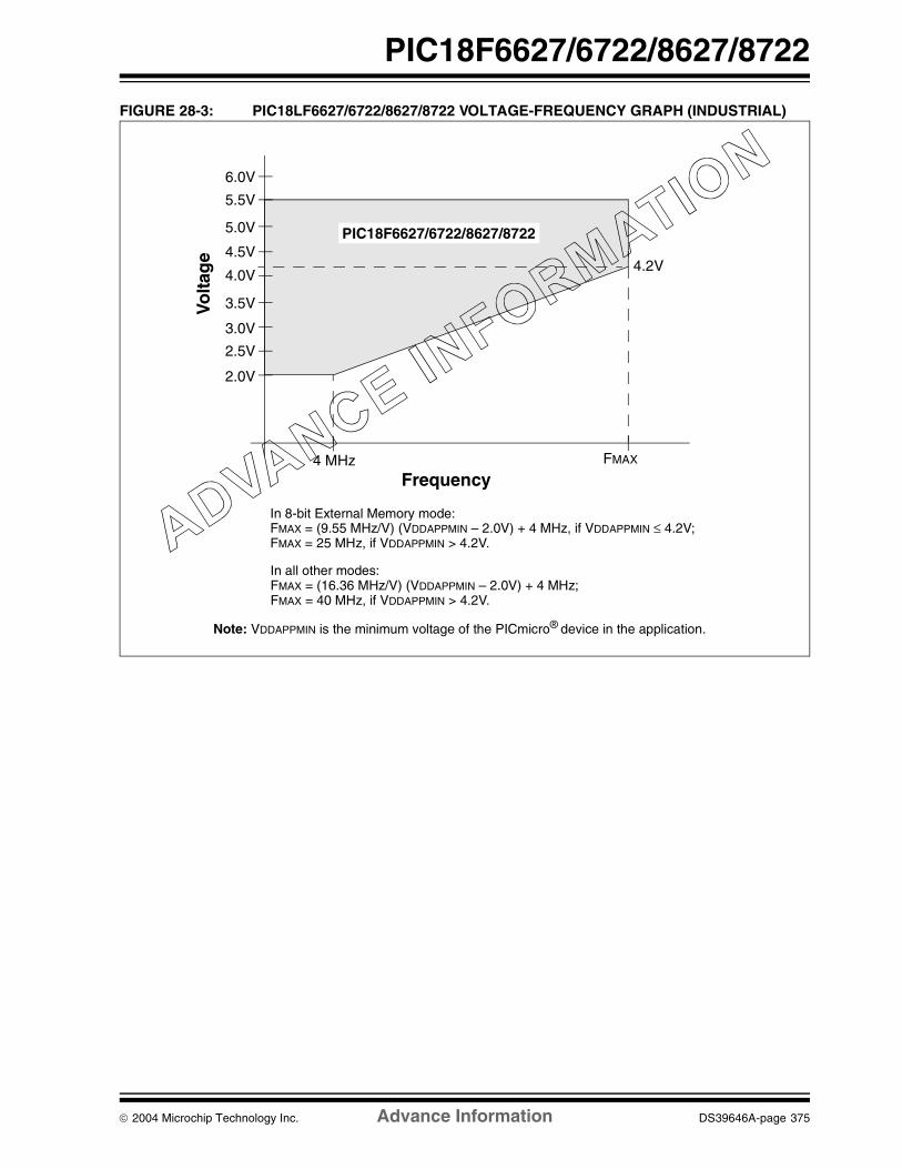
2004 Microchip Technology Inc. Advance Information DS39646A-page 375
PIC18F6627/6722/8627/8722
FIGURE 28-3: PIC18LF6627/6722/8627/8722 VOLTAGE-FREQUENCY GRAPH (INDUSTRIAL)
Frequency
Vo
ltag
e
6.0V
5.5V
4.5V
4.0V
2.0V
FMAX
5.0V
3.5V
3.0V
2.5V
In 8-bit External Memory mode:
Note: VDDAPPMIN is the minimum voltage of the PICmicro® device in the application.
4 MHz
4.2V
PIC18F6627/6722/8627/8722
FMAX = (9.55 MHz/V) (VDDAPPMIN – 2.0V) + 4 MHz, if VDDAPPMIN ≤ 4.2V;FMAX = 25 MHz, if VDDAPPMIN > 4.2V.
In all other modes:FMAX = (16.36 MHz/V) (VDDAPPMIN – 2.0V) + 4 MHz;FMAX = 40 MHz, if VDDAPPMIN > 4.2V.

PIC18F6627/6722/8627/8722
DS39646A-page 376 Advance Information 2004 Microchip Technology Inc.
28.1 DC Characteristics: Supply VoltagePIC18F6627/6722/8627/8722 (Industrial, Extended) PIC18LF6627/6722/8627/8722 (Industrial)
PIC18LF6627/6722/8627/8722 (Industrial)
Standard Operating Conditions (unless otherwise stated)Operating temperature -40°C ≤ TA ≤ +85°C for industrial
PIC18F6627/6722/8627/8722 (Industrial, Extended)
Standard Operating Conditions (unless otherwise stated)Operating temperature -40°C ≤ TA ≤ +85°C for industrial
-40°C ≤ TA ≤ +125°C for extended
Param No.
Symbol Characteristic Min Typ Max Units Conditions
VDD Supply Voltage
D001 PIC18LF6627/6722/8627/8722 2.0 — 5.5 V
PIC18F6627/6722/8627/8722 4.2 — 5.5 V
D002 VDR RAM Data RetentionVoltage(1)
1.5 — — V
D003 VPOR VDD Start Voltage to ensure internal Power-on Reset signal
— — 0.7 V See Section 4.3 “Power-on Reset (POR)” for details
D004 SVDD VDD Rise Rateto ensure internal Power-on Reset signal
0.05 — — V/ms See Section 4.3 “Power-on Reset (POR)” for details
VBOR Brown-out Reset Voltage
D005 PIC18LF6627/6722/8627/8722
BORV1:BORV0 = 11 TBD 2.05 TBD V
BORV1:BORV0 = 10 TBD 2.79 TBD V
All devices
BORV1:BORV0 = 01 TBD 4.33 TBD V
BORV1:BORV0 = 00 TBD 4.59 TBD V
Legend: TBD = To Be Determined. Shading of rows is to assist in readability of the table.Note 1: This is the limit to which VDD can be lowered in Sleep mode, or during a device Reset, without losing RAM data.

2004 Microchip Technology Inc. Advance Information DS39646A-page 377
PIC18F6627/6722/8627/8722
28.2 DC Characteristics: Power-Down and Supply CurrentPIC18F6627/6722/8627/8722 (Industrial, Extended) PIC18LF6627/6722/8627/8722 (Industrial)
PIC18LF6627/6722/8627/8722 (Industrial)
Standard Operating Conditions (unless otherwise stated)Operating temperature -40°C ≤ TA ≤ +85°C for industrial
PIC18F6627/6722/8627/8722 (Industrial, Extended)
Standard Operating Conditions (unless otherwise stated)Operating temperature -40°C ≤ TA ≤ +85°C for industrial
-40°C ≤ TA ≤ +125°C for extended
Param No.
Device Typ Max Units Conditions
Power-down Current (IPD)(1)
PIC18LF6627/6722/8627/8722 TBD TBD µA -40°CVDD = 2.0V,
(Sleep mode)TBD TBD µA +25°C
TBD TBD µA +85°C
PIC18LF6627/6722/8627/8722 TBD TBD µA -40°CVDD = 3.0V,
(Sleep mode)TBD TBD µA +25°C
TBD TBD µA +85°C
All devices TBD TBD µA -40°C
VDD = 5.0V,(Sleep mode)
TBD TBD µA +25°C
TBD TBD µA +85°C
Extended devices only TBD TBD µA +125°C
Legend: TBD = To Be Determined. Shading of rows is to assist in readability of the table.Note 1: The power-down current in Sleep mode does not depend on the oscillator type. Power-down current is measured with
the part in Sleep mode, with all I/O pins in high-impedance state and tied to VDD or VSS and all features that add delta current disabled (such as WDT, Timer1 Oscillator, BOR, etc.).
2: The supply current is mainly a function of operating voltage, frequency and mode. Other factors, such as I/O pin loading and switching rate, oscillator type and circuit, internal code execution pattern and temperature, also have an impact on the current consumption.The test conditions for all IDD measurements in active operation mode are:
OSC1 = external square wave, from rail-to-rail; all I/O pins tri-stated, pulled to VDD OR VSS;MCLR = VDD; WDT enabled/disabled as specified.
3: Low-power Timer1 oscillator selected.4: BOR and HLVD enable internal band gap reference. With both modules enabled, current consumption will be less than
the sum of both specifications.

PIC18F6627/6722/8627/8722
DS39646A-page 378 Advance Information 2004 Microchip Technology Inc.
Supply Current (IDD)(2)
PIC18LF6627/6722/8627/8722 TBD TBD µA -40°C
FOSC = 31 kHz(RC_RUN mode,
Internal oscillator source)
TBD TBD µA +25°C VDD = 2.0V
TBD TBD µA +85°C
PIC18LF6627/6722/8627/8722 TBD TBD µA -40°C
TBD TBD µA +25°C VDD = 3.0V
TBD TBD µA +85°C
All devices TBD TBD µA -40°C
VDD = 5.0VTBD TBD µA +25°C
TBD TBD µA +85°C
Extended devices only TBD TBD µA +125°C
PIC18LF6627/6722/8627/8722 TBD TBD µA -40°C
FOSC = 1 MHz(RC_RUN mode,
Internal oscillator source)
TBD TBD µA +25°C VDD = 2.0V
TBD TBD µA +85°C
PIC18LF6627/6722/8627/8722 TBD TBD mA -40°C
TBD TBD mA +25°C VDD = 3.0V
TBD TBD mA +85°C
All devices TBD TBD mA -40°C
VDD = 5.0VTBD TBD mA +25°C
TBD TBD mA +85°C
Extended devices only TBD TBD µA +125°C
28.2 DC Characteristics: Power-Down and Supply CurrentPIC18F6627/6722/8627/8722 (Industrial, Extended) PIC18LF6627/6722/8627/8722 (Industrial) (Continued)
PIC18LF6627/6722/8627/8722 (Industrial)
Standard Operating Conditions (unless otherwise stated)Operating temperature -40°C ≤ TA ≤ +85°C for industrial
PIC18F6627/6722/8627/8722 (Industrial, Extended)
Standard Operating Conditions (unless otherwise stated)Operating temperature -40°C ≤ TA ≤ +85°C for industrial
-40°C ≤ TA ≤ +125°C for extended
Param No.
Device Typ Max Units Conditions
Legend: TBD = To Be Determined. Shading of rows is to assist in readability of the table.Note 1: The power-down current in Sleep mode does not depend on the oscillator type. Power-down current is measured with
the part in Sleep mode, with all I/O pins in high-impedance state and tied to VDD or VSS and all features that add delta current disabled (such as WDT, Timer1 Oscillator, BOR, etc.).
2: The supply current is mainly a function of operating voltage, frequency and mode. Other factors, such as I/O pin loading and switching rate, oscillator type and circuit, internal code execution pattern and temperature, also have an impact on the current consumption.The test conditions for all IDD measurements in active operation mode are:
OSC1 = external square wave, from rail-to-rail; all I/O pins tri-stated, pulled to VDD OR VSS;MCLR = VDD; WDT enabled/disabled as specified.
3: Low-power Timer1 oscillator selected.4: BOR and HLVD enable internal band gap reference. With both modules enabled, current consumption will be less than
the sum of both specifications.

2004 Microchip Technology Inc. Advance Information DS39646A-page 379
PIC18F6627/6722/8627/8722
Supply Current (IDD)(2)
PIC18LF6627/6722/8627/8722 TBD TBD mA -40°C
FOSC = 4 MHz(RC_RUN mode,
Internal oscillator source)
TBD TBD mA +25°C VDD = 2.0V
TBD TBD mA +85°C
PIC18LF6627/6722/8627/8722 TBD TBD mA -40°C
TBD TBD mA +25°C VDD = 3.0V
TBD TBD mA +85°C
All devices TBD TBD mA -40°C
VDD = 5.0VTBD TBD mA +25°C
TBD TBD mA +85°C
Extended devices only TBD TBD µA +125°C
PIC18LF6627/6722/8627/8722 TBD TBD µA -40°C
FOSC = 31 kHz(RC_IDLE mode,
Internal oscillator source)
TBD TBD µA +25°C VDD = 2.0V
TBD TBD µA +85°C
PIC18LF6627/6722/8627/8722 TBD TBD µA -40°C
TBD TBD µA +25°C VDD = 3.0V
TBD TBD µA +85°C
All devices TBD TBD µA -40°C
VDD = 5.0VTBD TBD µA +25°C
TBD TBD µA +85°C
Extended devices only TBD TBD µA +125°C
28.2 DC Characteristics: Power-Down and Supply CurrentPIC18F6627/6722/8627/8722 (Industrial, Extended) PIC18LF6627/6722/8627/8722 (Industrial) (Continued)
PIC18LF6627/6722/8627/8722 (Industrial)
Standard Operating Conditions (unless otherwise stated)Operating temperature -40°C ≤ TA ≤ +85°C for industrial
PIC18F6627/6722/8627/8722 (Industrial, Extended)
Standard Operating Conditions (unless otherwise stated)Operating temperature -40°C ≤ TA ≤ +85°C for industrial
-40°C ≤ TA ≤ +125°C for extended
Param No.
Device Typ Max Units Conditions
Legend: TBD = To Be Determined. Shading of rows is to assist in readability of the table.Note 1: The power-down current in Sleep mode does not depend on the oscillator type. Power-down current is measured with
the part in Sleep mode, with all I/O pins in high-impedance state and tied to VDD or VSS and all features that add delta current disabled (such as WDT, Timer1 Oscillator, BOR, etc.).
2: The supply current is mainly a function of operating voltage, frequency and mode. Other factors, such as I/O pin loading and switching rate, oscillator type and circuit, internal code execution pattern and temperature, also have an impact on the current consumption.The test conditions for all IDD measurements in active operation mode are:
OSC1 = external square wave, from rail-to-rail; all I/O pins tri-stated, pulled to VDD OR VSS;MCLR = VDD; WDT enabled/disabled as specified.
3: Low-power Timer1 oscillator selected.4: BOR and HLVD enable internal band gap reference. With both modules enabled, current consumption will be less than
the sum of both specifications.

PIC18F6627/6722/8627/8722
DS39646A-page 380 Advance Information 2004 Microchip Technology Inc.
Supply Current (IDD)(2)
PIC18LF6627/6722/8627/8722 TBD TBD µA -40°C
FOSC = 1 MHz(RC_IDLE mode,
Internal oscillator source)
TBD TBD µA +25°C VDD = 2.0V
TBD TBD µA +85°C
PIC18LF6627/6722/8627/8722 TBD TBD µA -40°C
TBD TBD µA +25°C VDD = 3.0V
TBD TBD µA +85°C
All devices TBD TBD µA -40°C
VDD = 5.0VTBD TBD µA +25°C
TBD TBD µA +85°C
Extended devices only TBD TBD µA +125°C
PIC18LF6627/6722/8627/8722 TBD TBD µA -40°C
FOSC = 4 MHz(RC_IDLE mode,
Internal oscillator source)
TBD TBD µA +25°C VDD = 2.0V
TBD TBD µA +85°C
PIC18LF6627/6722/8627/8722 TBD TBD µA -40°C
TBD TBD µA +25°C VDD = 3.0V
TBD TBD µA +85°C
All devices TBD TBD mA -40°C
VDD = 5.0VTBD TBD mA +25°C
TBD TBD mA +85°C
Extended devices only TBD TBD µA +125°C
28.2 DC Characteristics: Power-Down and Supply CurrentPIC18F6627/6722/8627/8722 (Industrial, Extended) PIC18LF6627/6722/8627/8722 (Industrial) (Continued)
PIC18LF6627/6722/8627/8722 (Industrial)
Standard Operating Conditions (unless otherwise stated)Operating temperature -40°C ≤ TA ≤ +85°C for industrial
PIC18F6627/6722/8627/8722 (Industrial, Extended)
Standard Operating Conditions (unless otherwise stated)Operating temperature -40°C ≤ TA ≤ +85°C for industrial
-40°C ≤ TA ≤ +125°C for extended
Param No.
Device Typ Max Units Conditions
Legend: TBD = To Be Determined. Shading of rows is to assist in readability of the table.Note 1: The power-down current in Sleep mode does not depend on the oscillator type. Power-down current is measured with
the part in Sleep mode, with all I/O pins in high-impedance state and tied to VDD or VSS and all features that add delta current disabled (such as WDT, Timer1 Oscillator, BOR, etc.).
2: The supply current is mainly a function of operating voltage, frequency and mode. Other factors, such as I/O pin loading and switching rate, oscillator type and circuit, internal code execution pattern and temperature, also have an impact on the current consumption.The test conditions for all IDD measurements in active operation mode are:
OSC1 = external square wave, from rail-to-rail; all I/O pins tri-stated, pulled to VDD OR VSS;MCLR = VDD; WDT enabled/disabled as specified.
3: Low-power Timer1 oscillator selected.4: BOR and HLVD enable internal band gap reference. With both modules enabled, current consumption will be less than
the sum of both specifications.

2004 Microchip Technology Inc. Advance Information DS39646A-page 381
PIC18F6627/6722/8627/8722
Supply Current (IDD)(2)
PIC18LF6627/6722/8627/8722 TBD TBD µA -40°C
FOSC = 1 MHZ
(PRI_RUN,EC oscillator)
TBD TBD µA +25°C VDD = 2.0V
TBD TBD µA +85°C
PIC18LF6627/6722/8627/8722 TBD TBD µA -40°C
TBD TBD µA +25°C VDD = 3.0V
TBD TBD µA +85°C
All devices TBD TBD mA -40°C
VDD = 5.0VTBD TBD mA +25°C
TBD TBD mA +85°C
Extended devices only TBD TBD µA +125°C
PIC18LF6627/6722/8627/8722 TBD TBD mA -40°C
FOSC = 4 MHz(PRI_RUN,
EC oscillator)
TBD TBD mA +25°C VDD = 2.0V
TBD TBD mA +85°C
PIC18LF6627/6722/8627/8722 TBD TBD mA -40°C
TBD TBD mA +25°C VDD = 3.0V
TBD TBD mA +85°C
All devices TBD TBD mA -40°C
VDD = 5.0VTBD TBD mA +25°C
TBD TBD mA +85°C
Extended devices only TBD TBD µA +125°C
28.2 DC Characteristics: Power-Down and Supply CurrentPIC18F6627/6722/8627/8722 (Industrial, Extended) PIC18LF6627/6722/8627/8722 (Industrial) (Continued)
PIC18LF6627/6722/8627/8722 (Industrial)
Standard Operating Conditions (unless otherwise stated)Operating temperature -40°C ≤ TA ≤ +85°C for industrial
PIC18F6627/6722/8627/8722 (Industrial, Extended)
Standard Operating Conditions (unless otherwise stated)Operating temperature -40°C ≤ TA ≤ +85°C for industrial
-40°C ≤ TA ≤ +125°C for extended
Param No.
Device Typ Max Units Conditions
Legend: TBD = To Be Determined. Shading of rows is to assist in readability of the table.Note 1: The power-down current in Sleep mode does not depend on the oscillator type. Power-down current is measured with
the part in Sleep mode, with all I/O pins in high-impedance state and tied to VDD or VSS and all features that add delta current disabled (such as WDT, Timer1 Oscillator, BOR, etc.).
2: The supply current is mainly a function of operating voltage, frequency and mode. Other factors, such as I/O pin loading and switching rate, oscillator type and circuit, internal code execution pattern and temperature, also have an impact on the current consumption.The test conditions for all IDD measurements in active operation mode are:
OSC1 = external square wave, from rail-to-rail; all I/O pins tri-stated, pulled to VDD OR VSS;MCLR = VDD; WDT enabled/disabled as specified.
3: Low-power Timer1 oscillator selected.4: BOR and HLVD enable internal band gap reference. With both modules enabled, current consumption will be less than
the sum of both specifications.

PIC18F6627/6722/8627/8722
DS39646A-page 382 Advance Information 2004 Microchip Technology Inc.
Supply Current (IDD)(2)
Extended devices only TBD TBD mA +125°C VDD = 4.2V FOSC = 25 MHz(PRI_RUN,
EC oscillator)TBD TBD mA +125°C VDD = 5.0V
All devices TBD TBD mA -40°C
FOSC = 40 MHZ
(PRI_RUN,EC oscillator)
TBD TBD mA +25°C VDD = 4.2V
TBD TBD mA +85°C
All devices TBD TBD mA -40°C
TBD TBD mA +25°C VDD = 5.0V
TBD TBD mA +85°C
28.2 DC Characteristics: Power-Down and Supply CurrentPIC18F6627/6722/8627/8722 (Industrial, Extended) PIC18LF6627/6722/8627/8722 (Industrial) (Continued)
PIC18LF6627/6722/8627/8722 (Industrial)
Standard Operating Conditions (unless otherwise stated)Operating temperature -40°C ≤ TA ≤ +85°C for industrial
PIC18F6627/6722/8627/8722 (Industrial, Extended)
Standard Operating Conditions (unless otherwise stated)Operating temperature -40°C ≤ TA ≤ +85°C for industrial
-40°C ≤ TA ≤ +125°C for extended
Param No.
Device Typ Max Units Conditions
Legend: TBD = To Be Determined. Shading of rows is to assist in readability of the table.Note 1: The power-down current in Sleep mode does not depend on the oscillator type. Power-down current is measured with
the part in Sleep mode, with all I/O pins in high-impedance state and tied to VDD or VSS and all features that add delta current disabled (such as WDT, Timer1 Oscillator, BOR, etc.).
2: The supply current is mainly a function of operating voltage, frequency and mode. Other factors, such as I/O pin loading and switching rate, oscillator type and circuit, internal code execution pattern and temperature, also have an impact on the current consumption.The test conditions for all IDD measurements in active operation mode are:
OSC1 = external square wave, from rail-to-rail; all I/O pins tri-stated, pulled to VDD OR VSS;MCLR = VDD; WDT enabled/disabled as specified.
3: Low-power Timer1 oscillator selected.4: BOR and HLVD enable internal band gap reference. With both modules enabled, current consumption will be less than
the sum of both specifications.

2004 Microchip Technology Inc. Advance Information DS39646A-page 383
PIC18F6627/6722/8627/8722
Supply Current (IDD)(2)
All devices TBD TBD mA -40°C
VDD = 4.2VFOSC = 4 MHZ.16 MHz internal
(PRI_RUN HS+PLL)
TBD TBD mA +25°C
TBD TBD mA +85°C
Extended devices only TBD TBD mA +125°C
All devices TBD TBD mA -40°C
VDD = 5.0VFOSC = 4 MHZ,16 MHz internal
(PRI_RUN HS+PLL)
TBD TBD mA +25°C
TBD TBD mA +85°C
Extended devices only TBD TBD mA +125°C
All devices TBD TBD mA -40°C
VDD = 4.2VFOSC = 10 MHZ,40 MHz internal
(PRI_RUN HS+PLL)TBD TBD mA +25°C
TBD TBD mA +85°C
All devices TBD TBD mA -40°C
VDD = 5.0VFOSC = 10 MHZ,40 MHz internal
(PRI_RUN HS+PLL)TBD TBD mA +25°C
TBD TBD mA +85°C
28.2 DC Characteristics: Power-Down and Supply CurrentPIC18F6627/6722/8627/8722 (Industrial, Extended) PIC18LF6627/6722/8627/8722 (Industrial) (Continued)
PIC18LF6627/6722/8627/8722 (Industrial)
Standard Operating Conditions (unless otherwise stated)Operating temperature -40°C ≤ TA ≤ +85°C for industrial
PIC18F6627/6722/8627/8722 (Industrial, Extended)
Standard Operating Conditions (unless otherwise stated)Operating temperature -40°C ≤ TA ≤ +85°C for industrial
-40°C ≤ TA ≤ +125°C for extended
Param No.
Device Typ Max Units Conditions
Legend: TBD = To Be Determined. Shading of rows is to assist in readability of the table.Note 1: The power-down current in Sleep mode does not depend on the oscillator type. Power-down current is measured with
the part in Sleep mode, with all I/O pins in high-impedance state and tied to VDD or VSS and all features that add delta current disabled (such as WDT, Timer1 Oscillator, BOR, etc.).
2: The supply current is mainly a function of operating voltage, frequency and mode. Other factors, such as I/O pin loading and switching rate, oscillator type and circuit, internal code execution pattern and temperature, also have an impact on the current consumption.The test conditions for all IDD measurements in active operation mode are:
OSC1 = external square wave, from rail-to-rail; all I/O pins tri-stated, pulled to VDD OR VSS;MCLR = VDD; WDT enabled/disabled as specified.
3: Low-power Timer1 oscillator selected.4: BOR and HLVD enable internal band gap reference. With both modules enabled, current consumption will be less than
the sum of both specifications.

PIC18F6627/6722/8627/8722
DS39646A-page 384 Advance Information 2004 Microchip Technology Inc.
Supply Current (IDD)(2)
PIC18LF6627/6722/8627/8722 TBD TBD µA -40°C
FOSC = 1 MHz(PRI_IDLE mode,
EC oscillator)
TBD TBD µA +25°C VDD = 2.0V
TBD TBD µA +85°C
PIC18LF6627/6722/8627/8722 TBD TBD µA -40°C
TBD TBD µA +25°C VDD = 3.0V
TBD TBD µA +85°C
All devices TBD TBD µA -40°C
VDD = 5.0VTBD TBD µA +25°C
TBD TBD µA +85°C
Extended devices only TBD TBD µA +125°C
PIC18LF6627/6722/8627/8722 TBD TBD µA -40°C
FOSC = 4 MHz(PRI_IDLE mode,
EC oscillator)
TBD TBD µA +25°C VDD = 2.0V
TBD TBD µA +85°C
PIC18LF6627/6722/8627/8722 TBD TBD µA -40°C
TBD TBD µA +25°C VDD = 3.0V
TBD TBD µA +85°C
All devices TBD TBD mA -40°C
VDD = 5.0VTBD TBD mA +25°C
TBD TBD mA +85°C
Extended devices only TBD TBD µA +125°C
28.2 DC Characteristics: Power-Down and Supply CurrentPIC18F6627/6722/8627/8722 (Industrial, Extended) PIC18LF6627/6722/8627/8722 (Industrial) (Continued)
PIC18LF6627/6722/8627/8722 (Industrial)
Standard Operating Conditions (unless otherwise stated)Operating temperature -40°C ≤ TA ≤ +85°C for industrial
PIC18F6627/6722/8627/8722 (Industrial, Extended)
Standard Operating Conditions (unless otherwise stated)Operating temperature -40°C ≤ TA ≤ +85°C for industrial
-40°C ≤ TA ≤ +125°C for extended
Param No.
Device Typ Max Units Conditions
Legend: TBD = To Be Determined. Shading of rows is to assist in readability of the table.Note 1: The power-down current in Sleep mode does not depend on the oscillator type. Power-down current is measured with
the part in Sleep mode, with all I/O pins in high-impedance state and tied to VDD or VSS and all features that add delta current disabled (such as WDT, Timer1 Oscillator, BOR, etc.).
2: The supply current is mainly a function of operating voltage, frequency and mode. Other factors, such as I/O pin loading and switching rate, oscillator type and circuit, internal code execution pattern and temperature, also have an impact on the current consumption.The test conditions for all IDD measurements in active operation mode are:
OSC1 = external square wave, from rail-to-rail; all I/O pins tri-stated, pulled to VDD OR VSS;MCLR = VDD; WDT enabled/disabled as specified.
3: Low-power Timer1 oscillator selected.4: BOR and HLVD enable internal band gap reference. With both modules enabled, current consumption will be less than
the sum of both specifications.

2004 Microchip Technology Inc. Advance Information DS39646A-page 385
PIC18F6627/6722/8627/8722
Supply Current (IDD)(2)
Extended devices only TBD TBD mA +125°C VDD = 4.2V FOSC = 25 MHz(PRI_IDLE mode,
EC oscillator)TBD TBD mA +125°C VDD = 5.0V
All devices TBD TBD mA -40°C
FOSC = 40 MHz(PRI_IDLE mode,
EC oscillator)
TBD TBD mA +25°C VDD = 4.2 V
TBD TBD mA +85°C
All devices TBD TBD mA -40°C
TBD TBD mA +25°C VDD = 5.0V
TBD TBD mA +85°C
28.2 DC Characteristics: Power-Down and Supply CurrentPIC18F6627/6722/8627/8722 (Industrial, Extended) PIC18LF6627/6722/8627/8722 (Industrial) (Continued)
PIC18LF6627/6722/8627/8722 (Industrial)
Standard Operating Conditions (unless otherwise stated)Operating temperature -40°C ≤ TA ≤ +85°C for industrial
PIC18F6627/6722/8627/8722 (Industrial, Extended)
Standard Operating Conditions (unless otherwise stated)Operating temperature -40°C ≤ TA ≤ +85°C for industrial
-40°C ≤ TA ≤ +125°C for extended
Param No.
Device Typ Max Units Conditions
Legend: TBD = To Be Determined. Shading of rows is to assist in readability of the table.Note 1: The power-down current in Sleep mode does not depend on the oscillator type. Power-down current is measured with
the part in Sleep mode, with all I/O pins in high-impedance state and tied to VDD or VSS and all features that add delta current disabled (such as WDT, Timer1 Oscillator, BOR, etc.).
2: The supply current is mainly a function of operating voltage, frequency and mode. Other factors, such as I/O pin loading and switching rate, oscillator type and circuit, internal code execution pattern and temperature, also have an impact on the current consumption.The test conditions for all IDD measurements in active operation mode are:
OSC1 = external square wave, from rail-to-rail; all I/O pins tri-stated, pulled to VDD OR VSS;MCLR = VDD; WDT enabled/disabled as specified.
3: Low-power Timer1 oscillator selected.4: BOR and HLVD enable internal band gap reference. With both modules enabled, current consumption will be less than
the sum of both specifications.
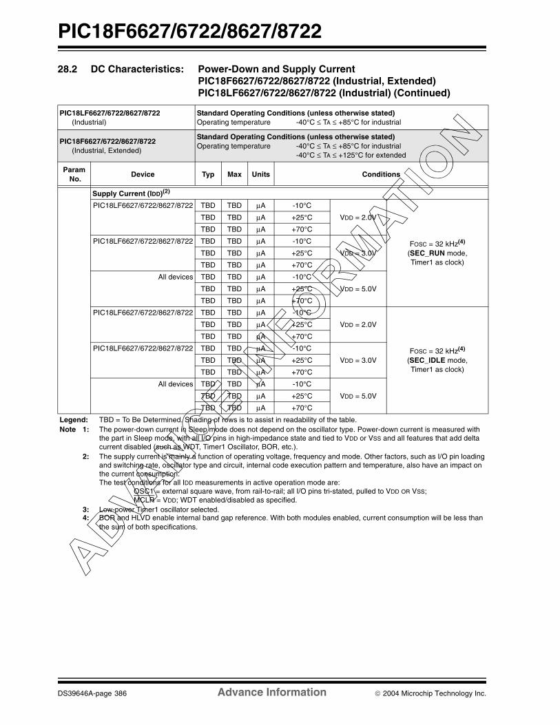
PIC18F6627/6722/8627/8722
DS39646A-page 386 Advance Information 2004 Microchip Technology Inc.
Supply Current (IDD)(2)
PIC18LF6627/6722/8627/8722 TBD TBD µA -10°C
FOSC = 32 kHz(4)
(SEC_RUN mode, Timer1 as clock)
TBD TBD µA +25°C VDD = 2.0V
TBD TBD µA +70°C
PIC18LF6627/6722/8627/8722 TBD TBD µA -10°C
TBD TBD µA +25°C VDD = 3.0V
TBD TBD µA +70°C
All devices TBD TBD µA -10°C
TBD TBD µA +25°C VDD = 5.0V
TBD TBD µA +70°C
PIC18LF6627/6722/8627/8722 TBD TBD µA -10°C
FOSC = 32 kHz(4)
(SEC_IDLE mode, Timer1 as clock)
TBD TBD µA +25°C VDD = 2.0V
TBD TBD µA +70°C
PIC18LF6627/6722/8627/8722 TBD TBD µA -10°C
TBD TBD µA +25°C VDD = 3.0V
TBD TBD µA +70°C
All devices TBD TBD µA -10°C
TBD TBD µA +25°C VDD = 5.0V
TBD TBD µA +70°C
28.2 DC Characteristics: Power-Down and Supply CurrentPIC18F6627/6722/8627/8722 (Industrial, Extended) PIC18LF6627/6722/8627/8722 (Industrial) (Continued)
PIC18LF6627/6722/8627/8722 (Industrial)
Standard Operating Conditions (unless otherwise stated)Operating temperature -40°C ≤ TA ≤ +85°C for industrial
PIC18F6627/6722/8627/8722 (Industrial, Extended)
Standard Operating Conditions (unless otherwise stated)Operating temperature -40°C ≤ TA ≤ +85°C for industrial
-40°C ≤ TA ≤ +125°C for extended
Param No.
Device Typ Max Units Conditions
Legend: TBD = To Be Determined. Shading of rows is to assist in readability of the table.Note 1: The power-down current in Sleep mode does not depend on the oscillator type. Power-down current is measured with
the part in Sleep mode, with all I/O pins in high-impedance state and tied to VDD or VSS and all features that add delta current disabled (such as WDT, Timer1 Oscillator, BOR, etc.).
2: The supply current is mainly a function of operating voltage, frequency and mode. Other factors, such as I/O pin loading and switching rate, oscillator type and circuit, internal code execution pattern and temperature, also have an impact on the current consumption.The test conditions for all IDD measurements in active operation mode are:
OSC1 = external square wave, from rail-to-rail; all I/O pins tri-stated, pulled to VDD OR VSS;MCLR = VDD; WDT enabled/disabled as specified.
3: Low-power Timer1 oscillator selected.4: BOR and HLVD enable internal band gap reference. With both modules enabled, current consumption will be less than
the sum of both specifications.

2004 Microchip Technology Inc. Advance Information DS39646A-page 387
PIC18F6627/6722/8627/8722
Module Differential Currents (∆IWDT, ∆IBOR, ∆ILVD, ∆IOSCB, ∆IAD)D022(∆IWDT)
Watchdog Timer TBD TBD µA -40°CVDD = 2.0VTBD TBD µA +25°C
TBD TBD µA +85°C
TBD TBD µA -40°CVDD = 3.0VTBD TBD µA +25°C
TBD TBD µA +85°C
TBD TBD µA -40°C
VDD = 5.0VTBD TBD µA +25°C
TBD TBD µA +85°C
TBD TBD µA +125°C
D022A(∆IBOR)
Brown-out Reset(4) TBD TBD µA -40°C to +85°C VDD = 3.0V
TBD TBD µA -40°C to +85°C
VDD = 5.0VTBD TBD µA -40°C to +125°C
TBD TBD µA -40°C to +85°C Sleep mode,BOREN1:BOREN0 = 10TBD TBD µA -40°C to +125°C
D022B(∆ILVD)
High/Low-Voltage Detect(4) TBD TBD µA -40°C to +85°C VDD = 2.0V
TBD TBD µA -40°C to +85°C VDD = 3.0V
TBD TBD µA -40°C to +85°CVDD = 5.0V
TBD TBD µA -40°C to +125°C
D025(∆IOSCB)
Timer1 Oscillator TBD TBD µA -40°CVDD = 2.0V 32 kHz on Timer1(3)TBD TBD µA +25°C
TBD TBD µA +85°C
TBD TBD µA -40°CVDD = 3.0V 32 kHz on Timer1(3)TBD TBD µA +25°C
TBD TBD µA +85°C
TBD TBD µA -40°CVDD = 5.0V 32 kHz on Timer1(3)TBD TBD µA +25°C
TBD TBD µA +85°C
28.2 DC Characteristics: Power-Down and Supply CurrentPIC18F6627/6722/8627/8722 (Industrial, Extended) PIC18LF6627/6722/8627/8722 (Industrial) (Continued)
PIC18LF6627/6722/8627/8722 (Industrial)
Standard Operating Conditions (unless otherwise stated)Operating temperature -40°C ≤ TA ≤ +85°C for industrial
PIC18F6627/6722/8627/8722 (Industrial, Extended)
Standard Operating Conditions (unless otherwise stated)Operating temperature -40°C ≤ TA ≤ +85°C for industrial
-40°C ≤ TA ≤ +125°C for extended
Param No.
Device Typ Max Units Conditions
Legend: TBD = To Be Determined. Shading of rows is to assist in readability of the table.Note 1: The power-down current in Sleep mode does not depend on the oscillator type. Power-down current is measured with
the part in Sleep mode, with all I/O pins in high-impedance state and tied to VDD or VSS and all features that add delta current disabled (such as WDT, Timer1 Oscillator, BOR, etc.).
2: The supply current is mainly a function of operating voltage, frequency and mode. Other factors, such as I/O pin loading and switching rate, oscillator type and circuit, internal code execution pattern and temperature, also have an impact on the current consumption.The test conditions for all IDD measurements in active operation mode are:
OSC1 = external square wave, from rail-to-rail; all I/O pins tri-stated, pulled to VDD OR VSS;MCLR = VDD; WDT enabled/disabled as specified.
3: Low-power Timer1 oscillator selected.4: BOR and HLVD enable internal band gap reference. With both modules enabled, current consumption will be less than
the sum of both specifications.

PIC18F6627/6722/8627/8722
DS39646A-page 388 Advance Information 2004 Microchip Technology Inc.
D026(∆IAD)
A/D Converter TBD TBD µA -40°C to +85°C VDD = 2.0V
A/D on, not converting, Sleep mode
TBD TBD µA -40°C to +85°C VDD = 3.0V
TBD TBD µA -40°C to +85°CVDD = 5.0V
TBD TBD µA -40°C to +125°C
D027(∆ICOMP)
Comparator TBD TBD µA -40°CVDD = 2.0VTBD TBD µA +25°C
TBD TBD µA +85°C
TBD TBD µA -40°CVDD = 3.0VTBD TBD µA +25°C
TBD TBD µA +85°C
TBD TBD µA -40°C
VDD = 5.0VTBD TBD µA +25°C
TBD TBD µA +85°C
TBD TBD µA +125°C
28.2 DC Characteristics: Power-Down and Supply CurrentPIC18F6627/6722/8627/8722 (Industrial, Extended) PIC18LF6627/6722/8627/8722 (Industrial) (Continued)
PIC18LF6627/6722/8627/8722 (Industrial)
Standard Operating Conditions (unless otherwise stated)Operating temperature -40°C ≤ TA ≤ +85°C for industrial
PIC18F6627/6722/8627/8722 (Industrial, Extended)
Standard Operating Conditions (unless otherwise stated)Operating temperature -40°C ≤ TA ≤ +85°C for industrial
-40°C ≤ TA ≤ +125°C for extended
Param No.
Device Typ Max Units Conditions
Legend: TBD = To Be Determined. Shading of rows is to assist in readability of the table.Note 1: The power-down current in Sleep mode does not depend on the oscillator type. Power-down current is measured with
the part in Sleep mode, with all I/O pins in high-impedance state and tied to VDD or VSS and all features that add delta current disabled (such as WDT, Timer1 Oscillator, BOR, etc.).
2: The supply current is mainly a function of operating voltage, frequency and mode. Other factors, such as I/O pin loading and switching rate, oscillator type and circuit, internal code execution pattern and temperature, also have an impact on the current consumption.The test conditions for all IDD measurements in active operation mode are:
OSC1 = external square wave, from rail-to-rail; all I/O pins tri-stated, pulled to VDD OR VSS;MCLR = VDD; WDT enabled/disabled as specified.
3: Low-power Timer1 oscillator selected.4: BOR and HLVD enable internal band gap reference. With both modules enabled, current consumption will be less than
the sum of both specifications.

2004 Microchip Technology Inc. Advance Information DS39646A-page 389
PIC18F6627/6722/8627/8722
28.3 DC Characteristics: PIC18F6627/6722/8627/8722 (Industrial) PIC18LF6627/6722/8627/8722 (Industrial)
DC CHARACTERISTICSStandard Operating Conditions (unless otherwise stated)Operating temperature -40°C ≤ TA ≤ +85°C for industrial
ParamNo.
Symbol Characteristic Min Max Units Conditions
VIL Input Low Voltage
I/O ports:
D030 with TTL buffer VSS 0.15 VDD V VDD < 4.5V
D030A — 0.8 V 4.5V ≤ VDD ≤ 5.5V
D031 with Schmitt Trigger buffer VSS 0.2 VDD V
D032 MCLR VSS 0.2 VDD V
D033 OSC1 VSS 0.3 VDD V HS, HSPLL modes
D033AD033BD034
OSC1 OSC1T13CKI
VSS
VSS
VSS
0.2 VDD
0.30.3
VVV
RC, EC modes(1)
XT, LP modes
VIH Input High Voltage
I/O ports:
D040 with TTL buffer 0.25 VDD + 0.8V VDD V VDD < 4.5V
D040A 2.0 VDD V 4.5V ≤ VDD ≤ 5.5V
D041 with Schmitt Trigger buffer 0.8 VDD VDD V
D042 MCLR 0.8 VDD VDD V
D043 OSC1 0.7 VDD VDD V HS, HSPLL modes
D043AD043BD043CD044
OSC1OSC1OSC1T13CKI
0.8 VDD
0.9 VDD
1.61.6
VDD
VDD
VDD
VDD
VVVV
EC modeRC mode(1)
XT, LP modes
IIL Input Leakage Current(2,3)
D060 I/O ports — ±1 µA VSS ≤ VPIN ≤ VDD, Pin at high-impedance
D061 MCLR — ±5 µA Vss ≤ VPIN ≤ VDD
D063 OSC1 — ±5 µA Vss ≤ VPIN ≤ VDD
IPU Weak Pull-up Current
D070 IPURB PORTB weak pull-up current 50 400 µA VDD = 5V, VPIN = VSS
Note 1: In RC oscillator configuration, the OSC1/CLKI pin is a Schmitt Trigger input. It is not recommended that the PICmicro® device be driven with an external clock while in RC mode.
2: The leakage current on the MCLR pin is strongly dependent on the applied voltage level. The specified levels represent normal operating conditions. Higher leakage current may be measured at different input voltages.
3: Negative current is defined as current sourced by the pin.
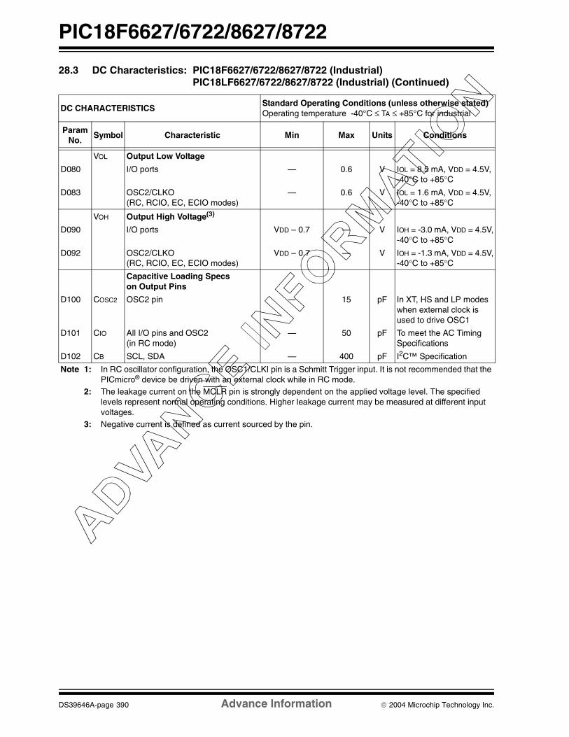
PIC18F6627/6722/8627/8722
DS39646A-page 390 Advance Information 2004 Microchip Technology Inc.
VOL Output Low Voltage
D080 I/O ports — 0.6 V IOL = 8.5 mA, VDD = 4.5V, -40°C to +85°C
D083 OSC2/CLKO(RC, RCIO, EC, ECIO modes)
— 0.6 V IOL = 1.6 mA, VDD = 4.5V, -40°C to +85°C
VOH Output High Voltage(3)
D090 I/O ports VDD – 0.7 — V IOH = -3.0 mA, VDD = 4.5V,-40°C to +85°C
D092 OSC2/CLKO (RC, RCIO, EC, ECIO modes)
VDD – 0.7 — V IOH = -1.3 mA, VDD = 4.5V,-40°C to +85°C
Capacitive Loading Specson Output Pins
D100 COSC2 OSC2 pin — 15 pF In XT, HS and LP modes when external clock is used to drive OSC1
D101 CIO All I/O pins and OSC2 (in RC mode)
— 50 pF To meet the AC Timing Specifications
D102 CB SCL, SDA — 400 pF I2C™ Specification
28.3 DC Characteristics: PIC18F6627/6722/8627/8722 (Industrial) PIC18LF6627/6722/8627/8722 (Industrial) (Continued)
DC CHARACTERISTICSStandard Operating Conditions (unless otherwise stated)Operating temperature -40°C ≤ TA ≤ +85°C for industrial
ParamNo.
Symbol Characteristic Min Max Units Conditions
Note 1: In RC oscillator configuration, the OSC1/CLKI pin is a Schmitt Trigger input. It is not recommended that the PICmicro® device be driven with an external clock while in RC mode.
2: The leakage current on the MCLR pin is strongly dependent on the applied voltage level. The specified levels represent normal operating conditions. Higher leakage current may be measured at different input voltages.
3: Negative current is defined as current sourced by the pin.

2004 Microchip Technology Inc. Advance Information DS39646A-page 391
PIC18F6627/6722/8627/8722
TABLE 28-1: MEMORY PROGRAMMING REQUIREMENTS
DC CHARACTERISTICSStandard Operating Conditions (unless otherwise stated)Operating temperature -40°C ≤ TA ≤ +85°C for industrial
ParamNo.
Sym Characteristic Min Typ† Max Units Conditions
Data EEPROM Memory
D120 ED Byte Endurance 100K 1M — E/W -40°C to +85°CD121 VDRW VDD for Read/Write VMIN — 5.5 V Using EECON to read/write
VMIN = Minimum operating voltage
D122 TDEW Erase/Write Cycle Time — 4 — ms
D123 TRETD Characteristic Retention 40 — — Year Provided no other specifications are violated
D124 TREF Number of Total Erase/Write Cycles before Refresh(1)
1M 10M — E/W -40°C to +85°C
D125 IDDP Supply Current during Programming
— 10 — mA
Program Flash Memory
D130 EP Cell Endurance 10K 100K — E/W -40°C to +85°CD131 VPR VDD for Read VMIN — 5.5 V VMIN = Minimum operating
voltage
D132B VPEW VDD for Self-timed Write VMIN — 5.5 V VMIN = Minimum operating voltage
D133A TIW Self-timed Write Cycle Time — 2 — ms
D134 TRETD Characteristic Retention 40 100 — Year Provided no other specifications are violated
D135 IDDP Supply Current during Programming
— 10 — mA
† Data in “Typ” column is at 5.0V, 25°C unless otherwise stated. These parameters are for design guidance only and are not tested.
Note 1: Refer to Section 8.8 “Using the Data EEPROM” for a more detailed discussion on data EEPROM endurance.

PIC18F6627/6722/8627/8722
DS39646A-page 392 Advance Information 2004 Microchip Technology Inc.
TABLE 28-2: COMPARATOR SPECIFICATIONS
TABLE 28-3: VOLTAGE REFERENCE SPECIFICATIONS
Operating Conditions: 3.0V < VDD < 5.5V, -40°C < TA < +85°C, unless otherwise stated.
ParamNo.
Sym Characteristics Min Typ Max Units Comments
D300 VIOFF Input Offset Voltage — ± 5.0 ± 10 mV
D301 VICM Input Common Mode Voltage 0 — VDD – 1.5 V
D302 CMRR Common Mode Rejection Ratio 55 — — dB
300 TRESP Response Time(1) — 150 400 ns PIC18FXXXX
300A — 150 600 ns PIC18LFXXXX,VDD = 2.0V
301 TMC2OV Comparator Mode Change to Output Valid
— — 10 µs
Note 1: Response time measured with one comparator input at (VDD – 1.5)/2, while the other input transitions from VSS to VDD.
Operating Conditions: 3.0V < VDD < 5.5V, -40°C < TA < +85°C (unless otherwise stated).
ParamNo.
Sym Characteristics Min Typ Max Units Comments
D310 VRES Resolution VDD/24 — VDD/32 LSb
D311 VRAA Absolute Accuracy — — 1/2 LSb
D312 VRUR Unit Resistor Value (R) — 2k — Ω310 TSET Settling Time(1) — — 10 µs
Note 1: Settling time measured while CVRR = 1 and CVR3:CVR0 transitions from ‘0000’ to ‘1111’.
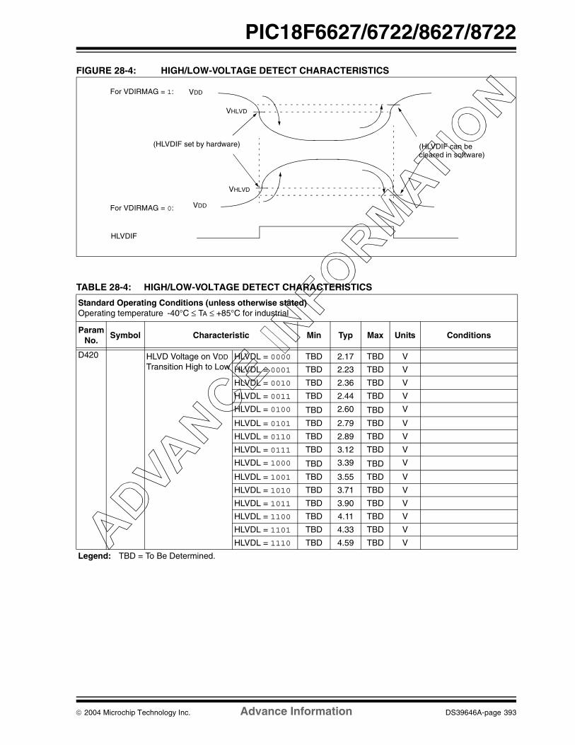
2004 Microchip Technology Inc. Advance Information DS39646A-page 393
PIC18F6627/6722/8627/8722
FIGURE 28-4: HIGH/LOW-VOLTAGE DETECT CHARACTERISTICS
TABLE 28-4: HIGH/LOW-VOLTAGE DETECT CHARACTERISTICS
VHLVD
HLVDIF
VDD
(HLVDIF set by hardware) (HLVDIF can be cleared in software)
VHLVD
For VDIRMAG = 1:
For VDIRMAG = 0: VDD
Standard Operating Conditions (unless otherwise stated)Operating temperature -40°C ≤ TA ≤ +85°C for industrial
Param No.
Symbol Characteristic Min Typ Max Units Conditions
D420 HLVD Voltage on VDD Transition High to Low
HLVDL = 0000 TBD 2.17 TBD V
HLVDL = 0001 TBD 2.23 TBD V
HLVDL = 0010 TBD 2.36 TBD V
HLVDL = 0011 TBD 2.44 TBD V
HLVDL = 0100 TBD 2.60 TBD V
HLVDL = 0101 TBD 2.79 TBD V
HLVDL = 0110 TBD 2.89 TBD V
HLVDL = 0111 TBD 3.12 TBD V
HLVDL = 1000 TBD 3.39 TBD V
HLVDL = 1001 TBD 3.55 TBD V
HLVDL = 1010 TBD 3.71 TBD V
HLVDL = 1011 TBD 3.90 TBD V
HLVDL = 1100 TBD 4.11 TBD V
HLVDL = 1101 TBD 4.33 TBD V
HLVDL = 1110 TBD 4.59 TBD V
Legend: TBD = To Be Determined.
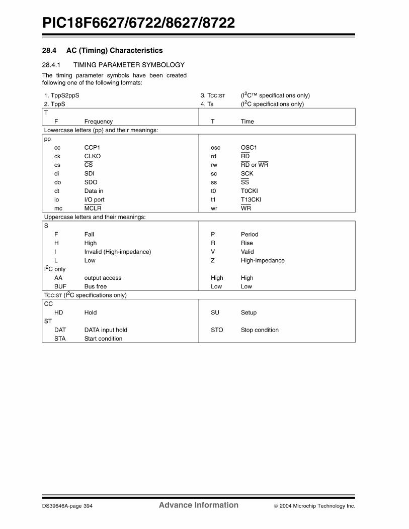
PIC18F6627/6722/8627/8722
DS39646A-page 394 Advance Information 2004 Microchip Technology Inc.
28.4 AC (Timing) Characteristics
28.4.1 TIMING PARAMETER SYMBOLOGY
The timing parameter symbols have been createdfollowing one of the following formats:
1. TppS2ppS 3. TCC:ST (I2C™ specifications only)2. TppS 4. Ts (I2C specifications only)T
F Frequency T TimeLowercase letters (pp) and their meanings:pp
cc CCP1 osc OSC1ck CLKO rd RDcs CS rw RD or WR
di SDI sc SCKdo SDO ss SSdt Data in t0 T0CKI
io I/O port t1 T13CKImc MCLR wr WR
Uppercase letters and their meanings:
SF Fall P PeriodH High R Rise
I Invalid (High-impedance) V ValidL Low Z High-impedance
I2C only
AA output access High HighBUF Bus free Low Low
TCC:ST (I2C specifications only)
CCHD Hold SU Setup
ST
DAT DATA input hold STO Stop conditionSTA Start condition

2004 Microchip Technology Inc. Advance Information DS39646A-page 395
PIC18F6627/6722/8627/8722
28.4.2 TIMING CONDITIONS
The temperature and voltages specified in Table 28-5apply to all timing specifications unless otherwisenoted. Figure 28-5 specifies the load conditions for thetiming specifications.
TABLE 28-5: TEMPERATURE AND VOLTAGE SPECIFICATIONS – AC
FIGURE 28-5: LOAD CONDITIONS FOR DEVICE TIMING SPECIFICATIONS
Note: Because of space limitations, the genericterms “PIC18FXXXX” and “PIC18LFXXXX”are used throughout this section to refer tothe PIC18F6627/6722/8627/8722 andPIC18LF6627/6722/8627/8722 families ofdevices specifically and only those devices.
AC CHARACTERISTICS
Standard Operating Conditions (unless otherwise stated)Operating temperature -40°C ≤ TA ≤ +85°C for industrialOperating voltage VDD range as described in DC spec Section 28.1 and Section 28.3. LF parts operate for industrial temperatures only.
VDD/2
CL
RL
Pin
Pin
VSS
VSS
CL
RL = 464Ω
CL = 50 pF for all pins except OSC2/CLKOand including D and E outputs as ports
Load Condition 1 Load Condition 2

PIC18F6627/6722/8627/8722
DS39646A-page 396 Advance Information 2004 Microchip Technology Inc.
28.4.3 TIMING DIAGRAMS AND SPECIFICATIONS
FIGURE 28-6: EXTERNAL CLOCK TIMING (ALL MODES EXCEPT PLL)
TABLE 28-6: EXTERNAL CLOCK TIMING REQUIREMENTS
OSC1
CLKO
Q4 Q1 Q2 Q3 Q4 Q1
1
2
3 3 4 4
Param.No.
Symbol Characteristic Min Max Units Conditions
1A FOSC External CLKI Frequency(1) DC 1 MHz XT, RC Oscillator mode
DC 25 MHz HS Oscillator mode
DC 31.25 kHz LP Oscillator mode
DC 40 MHz EC Oscillator mode
Oscillator Frequency(1) DC 4 MHz RC Oscillator mode
0.1 4 MHz XT Oscillator mode
4 25 MHz HS Oscillator mode
4 10 MHz HS + PLL Oscillator mode
5 200 kHz LP Oscillator mode
1 TOSC External CLKI Period(1) 1000 — ns XT, RC Oscillator mode
40 — ns HS Oscillator mode
32 — µs LP Oscillator mode
25 — ns EC Oscillator mode
Oscillator Period(1) 250 — ns RC Oscillator mode
250 1 µs XT Oscillator mode
40 250 ns HS Oscillator mode
100 250 ns HS + PLL Oscillator mode
5 — µs LP Oscillator mode
2 TCY Instruction Cycle Time(1) 100 — ns TCY = 4/FOSC, Industrial
160 — ns TCY = 4/FOSC, Extended
3 TOSL,TOSH
External Clock in (OSC1) High or Low Time
30 — ns XT Oscillator mode
2.5 — µs LP Oscillator mode
10 — ns HS Oscillator mode
4 TOSR,TOSF
External Clock in (OSC1) Rise or Fall Time
— 20 ns XT Oscillator mode
— 50 ns LP Oscillator mode
— 7.5 ns HS Oscillator mode
Note 1: Instruction cycle period (TCY) equals four times the input oscillator time base period for all configurations except PLL. All specified values are based on characterization data for that particular oscillator type under standard operating conditions with the device executing code. Exceeding these specified limits may result in an unstable oscillator operation and/or higher than expected current consumption. All devices are tested to operate at “min.” values with an external clock applied to the OSC1/CLKI pin. When an external clock input is used, the “max.” cycle time limit is “DC” (no clock) for all devices.
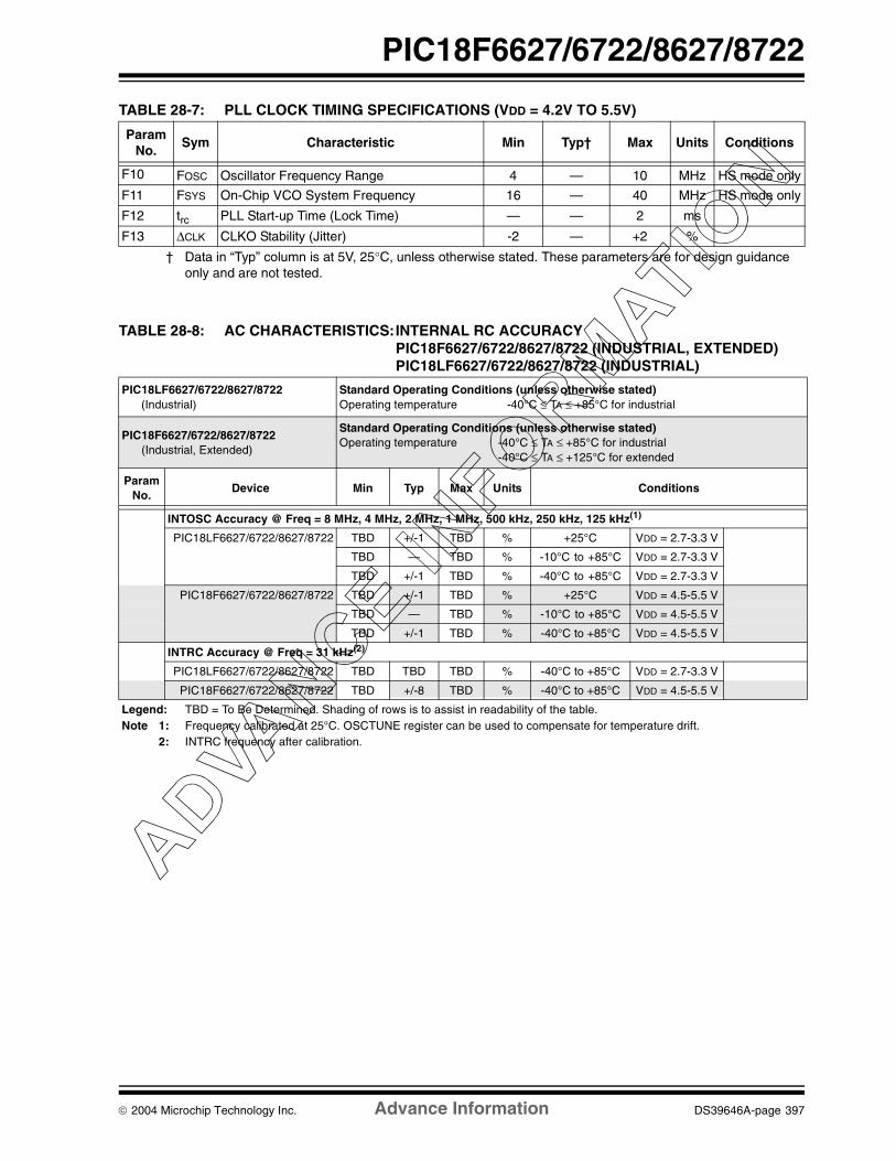
2004 Microchip Technology Inc. Advance Information DS39646A-page 397
PIC18F6627/6722/8627/8722
TABLE 28-7: PLL CLOCK TIMING SPECIFICATIONS (VDD = 4.2V TO 5.5V)
TABLE 28-8: AC CHARACTERISTICS:INTERNAL RC ACCURACYPIC18F6627/6722/8627/8722 (INDUSTRIAL, EXTENDED)PIC18LF6627/6722/8627/8722 (INDUSTRIAL)
Param No.
Sym Characteristic Min Typ† Max Units Conditions
F10 FOSC Oscillator Frequency Range 4 — 10 MHz HS mode only
F11 FSYS On-Chip VCO System Frequency 16 — 40 MHz HS mode only
F12 trc PLL Start-up Time (Lock Time) — — 2 ms
F13 ∆CLK CLKO Stability (Jitter) -2 — +2 %
† Data in “Typ” column is at 5V, 25°C, unless otherwise stated. These parameters are for design guidance only and are not tested.
PIC18LF6627/6722/8627/8722 (Industrial)
Standard Operating Conditions (unless otherwise stated)Operating temperature -40°C ≤ TA ≤ +85°C for industrial
PIC18F6627/6722/8627/8722 (Industrial, Extended)
Standard Operating Conditions (unless otherwise stated)Operating temperature -40°C ≤ TA ≤ +85°C for industrial
-40°C ≤ TA ≤ +125°C for extended
ParamNo.
Device Min Typ Max Units Conditions
INTOSC Accuracy @ Freq = 8 MHz, 4 MHz, 2 MHz, 1 MHz, 500 kHz, 250 kHz, 125 kHz(1)
PIC18LF6627/6722/8627/8722 TBD +/-1 TBD % +25°C VDD = 2.7-3.3 V
TBD — TBD % -10°C to +85°C VDD = 2.7-3.3 V
TBD +/-1 TBD % -40°C to +85°C VDD = 2.7-3.3 V
PIC18F6627/6722/8627/8722 TBD +/-1 TBD % +25°C VDD = 4.5-5.5 V
TBD — TBD % -10°C to +85°C VDD = 4.5-5.5 V
TBD +/-1 TBD % -40°C to +85°C VDD = 4.5-5.5 V
INTRC Accuracy @ Freq = 31 kHz(2)
PIC18LF6627/6722/8627/8722 TBD TBD TBD % -40°C to +85°C VDD = 2.7-3.3 V
PIC18F6627/6722/8627/8722 TBD +/-8 TBD % -40°C to +85°C VDD = 4.5-5.5 V
Legend: TBD = To Be Determined. Shading of rows is to assist in readability of the table.Note 1: Frequency calibrated at 25°C. OSCTUNE register can be used to compensate for temperature drift.
2: INTRC frequency after calibration.

PIC18F6627/6722/8627/8722
DS39646A-page 398 Advance Information 2004 Microchip Technology Inc.
FIGURE 28-7: CLKO AND I/O TIMING
TABLE 28-9: CLKO AND I/O TIMING REQUIREMENTS
Note: Refer to Figure 28-5 for load conditions.
OSC1
CLKO
I/O pin(Input)
I/O pin(Output)
Q4 Q1 Q2 Q3
10
1314
17
20, 21
19 18
15
11
12
16
Old Value New Value
ParamNo.
Symbol Characteristic Min Typ Max Units Conditions
10 TOSH2CKL OSC1 ↑ to CLKO ↓ — 75 200 ns (Note 1)
11 TOSH2CKH OSC1 ↑ to CLKO ↑ — 75 200 ns (Note 1)
12 TCKR CLKO Rise Time — 35 100 ns (Note 1)
13 TCKF CLKO Fall Time — 35 100 ns (Note 1)
14 TCKL2IOV CLKO ↓ to Port Out Valid — — 0.5 TCY + 20 ns (Note 1)
15 TIOV2CKH Port In Valid before CLKO ↑ 0.25 TCY + 25 — — ns (Note 1)
16 TCKH2IOI Port In Hold after CLKO ↑ 0 — — ns (Note 1)
17 TOSH2IOV OSC1↑ (Q1 cycle) to Port Out Valid — 50 150 ns
18 TOSH2IOI OSC1↑ (Q2 cycle) to Port Input Invalid (I/O in hold time)
PIC18FXXXX 100 — — ns
18A PIC18LFXXXX 200 — — ns VDD = 2.0V
19 TIOV2OSH Port Input Valid to OSC1↑ (I/O in setup time) 0 — — ns
20 TIOR Port Output Rise Time PIC18FXXXX — 10 25 ns
20A PIC18LFXXXX — — 60 ns VDD = 2.0V
21 TIOF Port Output Fall Time PIC18FXXXX — 10 25 ns
21A PIC18LFXXXX — — 60 ns VDD = 2.0V
22† TINP INT pin High or Low Time TCY — — ns
23† TRBP RB7:RB4 Change INT High or Low Time TCY — — ns
† These parameters are asynchronous events not related to any internal clock edges.Note 1: Measurements are taken in RC mode, where CLKO output is 4 x TOSC.

2004 Microchip Technology Inc. Advance Information DS39646A-page 399
PIC18F6627/6722/8627/8722
FIGURE 28-8: PROGRAM MEMORY READ TIMING DIAGRAM
TABLE 28-10: CLKO AND I/O TIMING REQUIREMENTS
Param. No
Symbol Characteristics Min Typ Max Units
150 TadV2alL Address Out Valid to ALE ↓ (address setup time)
0.25 TCY – 10 — — ns
151 TalL2adl ALE ↓ to Address Out Invalid (address hold time)
5 — — ns
155 TalL2oeL ALE ↓ to OE ↓ 10 0.125 TCY — ns
160 TadZ2oeL AD high-Z to OE ↓ (bus release to OE) 0 — — ns
161 ToeH2adD OE ↑ to AD Driven 0.125 TCY – 5 — — ns
162 TadV2oeH LS Data Valid before OE ↑ (data setup time) 20 — — ns
163 ToeH2adl OE ↑ to Data In Invalid (data hold time) 0 — — ns
164 TalH2alL ALE Pulse Width — TCY — ns
165 ToeL2oeH OE Pulse Width 0.5 TCY – 5 0.5 TCY — ns
166 TalH2alH ALE ↑ to ALE ↑ (cycle time) — 0.25 TCY — ns
167 Tacc Address Valid to Data Valid 0.75 TCY – 25 — — ns
168 Toe OE ↓ to Data Valid — 0.5 TCY – 25 ns
169 TalL2oeH ALE ↓ to OE ↑ 0.625 TCY – 10 — 0.625 TCY + 10 ns
171 TalH2csL Chip Enable Active to ALE ↓ 0.25 TCY – 20 — — ns
171A TubL2oeH AD Valid to Chip Enable Active — — 10 ns
Q1 Q2 Q3 Q4 Q1 Q2
OSC1
ALE
OE
Address Data from External
164
166
160
165
161151 162
163
AD<15:0>
167168
155
Address
Address
150
AD<19:16> Address
169
BA0
CE171
171A
Operating Conditions: 2.0V < VCC < 5.5V, -40°C < TA < +125°C unless otherwise stated.

PIC18F6627/6722/8627/8722
DS39646A-page 400 Advance Information 2004 Microchip Technology Inc.
FIGURE 28-9: PROGRAM MEMORY WRITE TIMING DIAGRAM
TABLE 28-11: PROGRAM MEMORY WRITE TIMING REQUIREMENTS
Param. No
Symbol Characteristics Min Typ Max Units
150 TadV2alL Address Out Valid to ALE ↓ (address setup time) 0.25 TCY – 10 — — ns
151 TalL2adl ALE ↓ to Address Out Invalid (address hold time) 5 — — ns
153 TwrH2adl WRn ↑ to Data Out Invalid (data hold time) 5 — — ns
154 TwrL WRn Pulse Width 0.5 TCY – 5 0.5 TCY — ns
156 TadV2wrH Data Valid before WRn ↑ (data setup time) 0.5 TCY – 10 — — ns
157 TbsV2wrL Byte Select Valid before WRn ↓ (byte select setup time)
0.25 TCY — — ns
157A TwrH2bsI WRn ↑ to Byte Select Invalid (byte select hold time) 0.125 TCY – 5 — — ns
166 TalH2alH ALE ↑ to ALE ↑ (cycle time) — 0.25 TCY — ns
171 TalH2csL Chip Enable Active to ALE ↓ 0.25 TCY – 20 — — ns
171A TubL2oeH AD Valid to Chip Enable Active — — 10 ns
Q1 Q2 Q3 Q4 Q1 Q2
OSC1
ALE
Address Data
156150
151
153
AD<15:0> Address
WRH orWRL
UB orLB
157
154
157A
AddressAD<19:16>
AddressBA0
166
CE
171
171A
Operating Conditions: 2.0V < VCC < 5.5V, -40°C < TA < +125°C unless otherwise stated.

2004 Microchip Technology Inc. Advance Information DS39646A-page 401
PIC18F6627/6722/8627/8722
FIGURE 28-10: RESET, WATCHDOG TIMER, OSCILLATOR START-UP TIMER AND POWER-UP TIMER TIMING
FIGURE 28-11: BROWN-OUT RESET TIMING
TABLE 28-12: RESET, WATCHDOG TIMER, OSCILLATOR START-UP TIMER, POWER-UP TIMER AND BROWN-OUT RESET REQUIREMENTS
Param. No.
Symbol Characteristic Min Typ Max Units Conditions
30 TmcL MCLR Pulse Width (low) 2 — — µs
31 TWDT Watchdog Timer Time-out Period (no postscaler)
3.4 4.0 4.6 ms
32 TOST Oscillation Start-up Timer Period 1024 TOSC — 1024 TOSC — TOSC = OSC1 period
33 TPWRT Power-up Timer Period 55.6 64 75 ms
34 TIOZ I/O High-Impedance from MCLR Low or Watchdog Timer Reset
— 2 — µs
35 TBOR Brown-out Reset Pulse Width 200 — — µs VDD ≤ BVDD (see D005)
36 TIVRST Time for Internal Reference Voltage to become Stable
— 20 50 µs
37 TLVD High/Low-Voltage Detect Pulse Width 200 — — µs VDD ≤ VLVD
38 TCSD CPU Start-up Time — 10 — µs
39 TIOBST Time for INTOSC to Stabilize — 1 — µs
VDD
MCLR
InternalPOR
PWRTTime-out
OSCTime-out
InternalReset
WatchdogTimerReset
33
32
30
3134
I/O pins
34
Note: Refer to Figure 28-5 for load conditions.
VDDBVDD
35VBGAP = 1.2V
VIRVST
Enable Internal
Internal Reference36
Reference Voltage
Voltage Stable

PIC18F6627/6722/8627/8722
DS39646A-page 402 Advance Information 2004 Microchip Technology Inc.
FIGURE 28-12: TIMER0 AND TIMER1 EXTERNAL CLOCK TIMINGS
TABLE 28-13: TIMER0 AND TIMER1 EXTERNAL CLOCK REQUIREMENTS
Note: Refer to Figure 28-5 for load conditions.
46
47
45
48
41
42
40
T0CKI
T1OSO/T13CKI
TMR0 orTMR1
Param No.
Symbol Characteristic Min Max Units Conditions
40 TT0H T0CKI High Pulse Width No prescaler 0.5 TCY + 20 — ns
With prescaler 10 — ns
41 TT0L T0CKI Low Pulse Width No prescaler 0.5 TCY + 20 — ns
With prescaler 10 — ns
42 TT0P T0CKI Period No prescaler TCY + 10 — ns
With prescaler Greater of:20 ns or
(TCY + 40)/N
— ns N = prescalevalue (1, 2, 4,..., 256)
45 TT1H T13CKI High Time
Synchronous, no prescaler 0.5 TCY + 20 — ns
Synchronous,with prescaler
PIC18FXXXX 10 — ns
PIC18LFXXXX 25 — ns VDD = 2.0V
Asynchronous PIC18FXXXX 30 — ns
PIC18LFXXXX 50 — ns VDD = 2.0V
46 TT1L T13CKI Low Time
Synchronous, no prescaler 0.5 TCY + 5 — ns
Synchronous, with prescaler
PIC18FXXXX 10 — ns
PIC18LFXXXX 25 — ns VDD = 2.0V
Asynchronous PIC18FXXXX 30 — ns
PIC18LFXXXX 50 — ns VDD = 2.0V
47 TT1P T13CKI Input Period
Synchronous Greater of:20 ns or
(TCY + 40)/N
— ns N = prescalevalue (1, 2, 4, 8)
Asynchronous 60 — ns
FT1 T13CKI Oscillator Input Frequency Range DC 50 kHz
48 TCKE2TMRI Delay from External T13CKI Clock Edge to Timer Increment
2 TOSC 7 TOSC —

2004 Microchip Technology Inc. Advance Information DS39646A-page 403
PIC18F6627/6722/8627/8722
FIGURE 28-13: CAPTURE/COMPARE/PWM TIMINGS (ALL ECCP/CCP MODULES)
TABLE 28-14: CAPTURE/COMPARE/PWM REQUIREMENTS (ALL CCP MODULES)
Note: Refer to Figure 28-5 for load conditions.
CCPx(Capture Mode)
50 51
52
CCPx
53 54
(Compare or PWM Mode)
Param No.
Symbol Characteristic Min Max Units Conditions
50 TCCL CCPx Input Low Time
No prescaler 0.5 TCY + 20 — ns
With prescaler
PIC18FXXXX 10 — ns
PIC18LFXXXX 20 — ns VDD = 2.0V
51 TCCH CCPx Input High Time
No prescaler 0.5 TCY + 20 — ns
Withprescaler
PIC18FXXXX 10 — ns
PIC18LFXXXX 20 — ns VDD = 2.0V
52 TCCP CCPx Input Period 3 TCY + 40N
— ns N = prescale value (1, 4 or 16)
53 TCCR CCPx Output Fall Time PIC18FXXXX — 25 ns
PIC18LFXXXX — 45 ns VDD = 2.0V
54 TCCF CCPx Output Fall Time PIC18FXXXX — 25 ns
PIC18LFXXXX — 45 ns VDD = 2.0V

PIC18F6627/6722/8627/8722
DS39646A-page 404 Advance Information 2004 Microchip Technology Inc.
FIGURE 28-14: PARALLEL SLAVE PORT TIMING (DEVICE FAMILY PSP)
TABLE 28-15: PARALLEL SLAVE PORT REQUIREMENTS (PIC18F8627/8722)
Note: Refer to Figure 28-5 for load conditions.
RE2/CS
RE0/RD
RE1/WR
RD7:RD0
62
63
64
65
Param.No.
Symbol Characteristic Min Max Units Conditions
62 TdtV2wrH Data In Valid before WR ↑ or CS ↑ (setup time) 20 — ns
63 TwrH2dtI WR ↑ or CS ↑ to Data–In Invalid (hold time)
PIC18FXXXX 20 — ns
PIC18LFXXXX 35 — ns VDD = 2.0V
64 TrdL2dtV RD ↓ and CS ↓ to Data–Out Valid — 80 ns
65 TrdH2dtI RD ↑ or CS ↓ to Data–Out Invalid 10 30 ns
66 TibfINH Inhibit of the IBF Flag bit being Cleared from WR ↑ or CS ↑
— 3 TCY

2004 Microchip Technology Inc. Advance Information DS39646A-page 405
PIC18F6627/6722/8627/8722
FIGURE 28-15: EXAMPLE SPI™ MASTER MODE TIMING (CKE = 0)
TABLE 28-16: EXAMPLE SPI™ MODE REQUIREMENTS (MASTER MODE, CKE = 0)
SS
SCK(CKP = 0)
SCK(CKP = 1)
SDO
SDI
70
71 72
7374
75, 76
787980
7978
MSb LSbbit 6 - - - - - - 1
MSb In LSb Inbit 6 - - - - 1
Note: Refer to Figure 28-5 for load conditions.
Param No.
Symbol Characteristic Min Max Units Conditions
70 TSSL2SCH, TSSL2SCL
SS ↓ to SCK ↓ or SCK ↑ Input TCY — ns
71 TSCH SCK Input High Time (Slave mode)
Continuous 1.25 TCY + 30 — ns
71A Single Byte 40 — ns (Note 1)
72 TSCL SCK Input Low Time (Slave mode)
Continuous 1.25 TCY + 30 — ns
72A Single Byte 40 — ns (Note 1)
73 TDIV2SCH, TDIV2SCL
Setup Time of SDI Data Input to SCK Edge 100 — ns
73A TB2B Last Clock Edge of Byte 1 to the 1st Clock Edge of Byte 2
1.5 TCY + 40 — ns (Note 2)
74 TSCH2DIL, TSCL2DIL
Hold Time of SDI Data Input to SCK Edge 100 — ns
75 TDOR SDO Data Output Rise Time PIC18FXXXX — 25 ns
PIC18LFXXXX — 45 ns VDD = 2.0V
76 TDOF SDO Data Output Fall Time — 25 ns
78 TSCR SCK Output Rise Time (Master mode)
PIC18FXXXX — 25 ns
PIC18LFXXXX — 45 ns VDD = 2.0V
79 TSCF SCK Output Fall Time (Master mode) — 25 ns
80 TSCH2DOV,TSCL2DOV
SDO Data Output Valid after SCK Edge
PIC18FXXXX — 50 ns
PIC18LFXXXX — 100 ns VDD = 2.0V
Note 1: Requires the use of Parameter #73A.2: Only if Parameter #71A and #72A are used.

PIC18F6627/6722/8627/8722
DS39646A-page 406 Advance Information 2004 Microchip Technology Inc.
FIGURE 28-16: EXAMPLE SPI™ MASTER MODE TIMING (CKE = 1)
TABLE 28-17: EXAMPLE SPI™ MODE REQUIREMENTS (MASTER MODE, CKE = 1)
SS
SCK(CKP = 0)
SCK(CKP = 1)
SDO
SDI
81
71 72
74
75, 76
78
80
MSb
7973
MSb In
bit 6 - - - - - - 1
LSb Inbit 6 - - - - 1
LSb
Note: Refer to Figure 28-5 for load conditions.
Param. No.
Symbol Characteristic Min Max Units Conditions
71 TSCH SCK Input High Time (Slave mode)
Continuous 1.25 TCY + 30 — ns
71A Single Byte 40 — ns (Note 1)
72 TSCL SCK Input Low Time (Slave mode)
Continuous 1.25 TCY + 30 — ns
72A Single Byte 40 — ns (Note 1)
73 TDIV2SCH, TDIV2SCL
Setup Time of SDI Data Input to SCK Edge 100 — ns
73A TB2B Last Clock Edge of Byte 1 to the 1st Clock Edge of Byte 2
1.5 TCY + 40 — ns (Note 2)
74 TSCH2DIL, TSCL2DIL
Hold Time of SDI Data Input to SCK Edge 100 — ns
75 TDOR SDO Data Output Rise Time PIC18FXXXX — 25 ns
PIC18LFXXXX — 45 ns VDD = 2.0V
76 TDOF SDO Data Output Fall Time — 25 ns
78 TSCR SCK Output Rise Time (Master mode)
PIC18FXXXX — 25 ns
PIC18LFXXXX — 45 ns VDD = 2.0V
79 TSCF SCK Output Fall Time (Master mode) — 25 ns
80 TSCH2DOV,TSCL2DOV
SDO Data Output Valid after SCK Edge
PIC18FXXXX — 50 ns
PIC18LFXXXX — 100 ns VDD = 2.0V
81 TDOV2SCH,TDOV2SCL
SDO Data Output Setup to SCK Edge TCY — ns
Note 1: Requires the use of Parameter #73A.
2: Only if Parameter #71A and #72A are used.
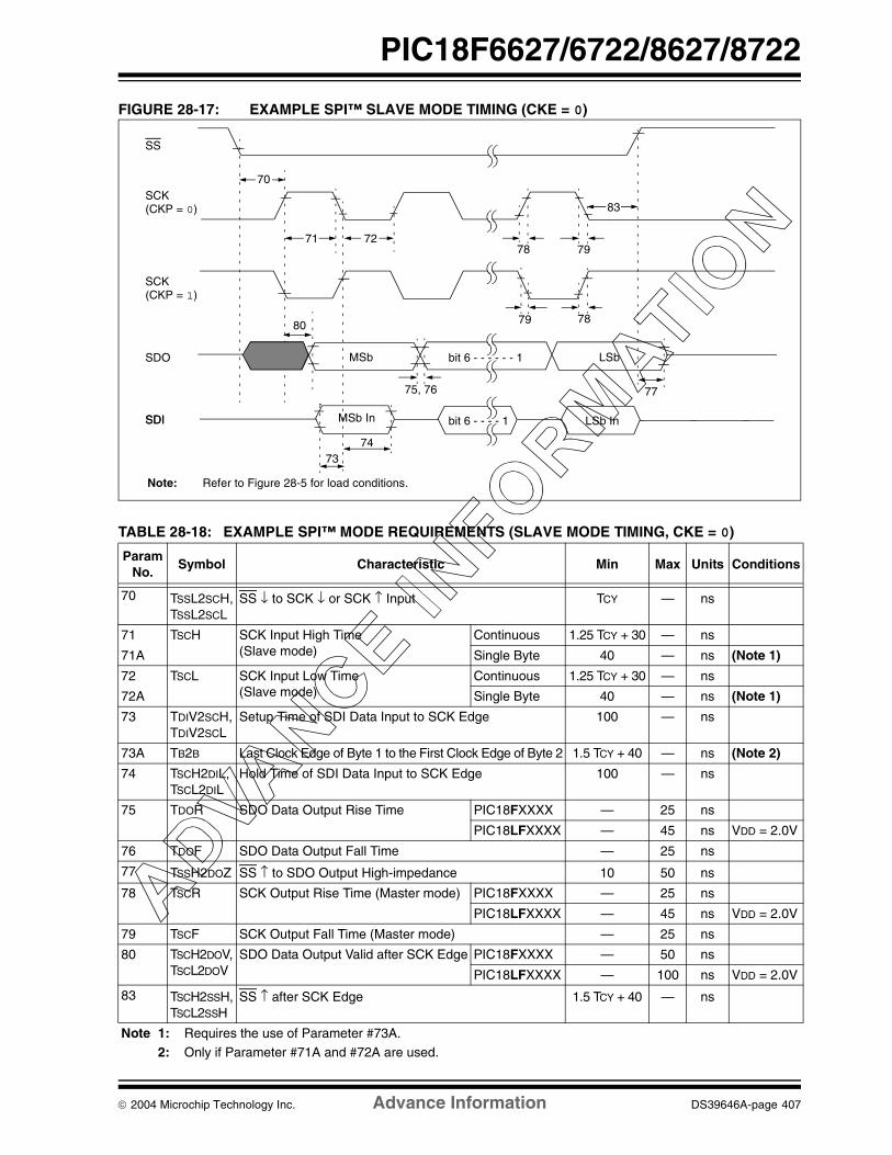
2004 Microchip Technology Inc. Advance Information DS39646A-page 407
PIC18F6627/6722/8627/8722
FIGURE 28-17: EXAMPLE SPI™ SLAVE MODE TIMING (CKE = 0)
TABLE 28-18: EXAMPLE SPI™ MODE REQUIREMENTS (SLAVE MODE TIMING, CKE = 0)
Param No.
Symbol Characteristic Min Max Units Conditions
70 TSSL2SCH, TSSL2SCL
SS ↓ to SCK ↓ or SCK ↑ Input TCY — ns
71 TSCH SCK Input High Time (Slave mode)
Continuous 1.25 TCY + 30 — ns
71A Single Byte 40 — ns (Note 1)
72 TSCL SCK Input Low Time (Slave mode)
Continuous 1.25 TCY + 30 — ns
72A Single Byte 40 — ns (Note 1)
73 TDIV2SCH, TDIV2SCL
Setup Time of SDI Data Input to SCK Edge 100 — ns
73A TB2B Last Clock Edge of Byte 1 to the First Clock Edge of Byte 2 1.5 TCY + 40 — ns (Note 2)
74 TSCH2DIL, TSCL2DIL
Hold Time of SDI Data Input to SCK Edge 100 — ns
75 TDOR SDO Data Output Rise Time PIC18FXXXX — 25 ns
PIC18LFXXXX — 45 ns VDD = 2.0V
76 TDOF SDO Data Output Fall Time — 25 ns
77 TSSH2DOZ SS ↑ to SDO Output High-impedance 10 50 ns
78 TSCR SCK Output Rise Time (Master mode) PIC18FXXXX — 25 ns
PIC18LFXXXX — 45 ns VDD = 2.0V
79 TSCF SCK Output Fall Time (Master mode) — 25 ns
80 TSCH2DOV,TSCL2DOV
SDO Data Output Valid after SCK Edge PIC18FXXXX — 50 ns
PIC18LFXXXX — 100 ns VDD = 2.0V
83 TSCH2SSH,TSCL2SSH
SS ↑ after SCK Edge 1.5 TCY + 40 — ns
Note 1: Requires the use of Parameter #73A.
2: Only if Parameter #71A and #72A are used.
SS
SCK(CKP = 0)
SCK(CKP = 1)
SDO
SDI
70
71 72
7374
75, 76 77
787980
7978
SDI
MSb LSbbit 6 - - - - - - 1
MSb In bit 6 - - - - 1 LSb In
83
Note: Refer to Figure 28-5 for load conditions.

PIC18F6627/6722/8627/8722
DS39646A-page 408 Advance Information 2004 Microchip Technology Inc.
FIGURE 28-18: EXAMPLE SPI™ SLAVE MODE TIMING (CKE = 1)
TABLE 28-19: EXAMPLE SPI™ SLAVE MODE REQUIREMENTS (CKE = 1)
ParamNo.
Symbol Characteristic Min Max Units Conditions
70 TSSL2SCH, TSSL2SCL
SS ↓ to SCK ↓ or SCK ↑ Input TCY — ns
71 TSCH SCK Input High Time (Slave mode)
Continuous 1.25 TCY + 30 — ns
71A Single Byte 40 — ns (Note 1)
72 TSCL SCK Input Low Time (Slave mode)
Continuous 1.25 TCY + 30 — ns
72A Single Byte 40 — ns (Note 1)
73A TB2B Last Clock Edge of Byte 1 to the First Clock Edge of Byte 2 1.5 TCY + 40 — ns (Note 2)
74 TSCH2DIL, TSCL2DIL
Hold Time of SDI Data Input to SCK Edge 100 — ns
75 TDOR SDO Data Output Rise Time PIC18FXXXX — 25 ns
PIC18LFXXXX — 45 ns VDD = 2.0V
76 TDOF SDO Data Output Fall Time — 25 ns
77 TSSH2DOZ SS↑ to SDO Output High-Impedance 10 50 ns
78 TSCR SCK Output Rise Time (Master mode)
PIC18FXXXX — 25 ns
PIC18LFXXXX — 45 ns VDD = 2.0V
79 TSCF SCK Output Fall Time (Master mode) — 25 ns
80 TSCH2DOV,TSCL2DOV
SDO Data Output Valid after SCK Edge
PIC18FXXXX — 50 ns
PIC18LFXXXX — 100 ns VDD = 2.0V
82 TSSL2DOV SDO Data Output Valid after SS ↓ Edge
PIC18FXXXX — 50 ns
PIC18LFXXXX — 100 ns VDD = 2.0V
83 TSCH2SSH,TSCL2SSH
SS ↑ after SCK Edge 1.5 TCY + 40 — ns
Note 1: Requires the use of Parameter #73A.2: Only if Parameter #71A and #72A are used.
SS
SCK(CKP = 0)
SCK(CKP = 1)
SDO
SDI
70
71 72
82
SDI
74
75, 76
MSb bit 6 - - - - - - 1 LSb
77
MSb In bit 6 - - - - 1 LSb In
80
83
Note: Refer to Figure 28-5 for load conditions.

2004 Microchip Technology Inc. Advance Information DS39646A-page 409
PIC18F6627/6722/8627/8722
FIGURE 28-19: I2C™ BUS START/STOP BITS TIMING
TABLE 28-20: I2C™ BUS START/STOP BITS REQUIREMENTS (SLAVE MODE)
FIGURE 28-20: I2C™ BUS DATA TIMING
Note: Refer to Figure 28-5 for load conditions.
91
92
93SCL
SDA
StartCondition
StopCondition
90
Param. No.
Symbol Characteristic Min Max Units Conditions
90 TSU:STA Start Condition 100 kHz mode 4700 — ns Only relevant for Repeated Start conditionSetup Time 400 kHz mode 600 —
91 THD:STA Start Condition 100 kHz mode 4000 — ns After this period, the first clock pulse is generatedHold Time 400 kHz mode 600 —
92 TSU:STO Stop Condition 100 kHz mode 4700 — ns
Setup Time 400 kHz mode 600 —
93 THD:STO Stop Condition 100 kHz mode 4000 — ns
Hold Time 400 kHz mode 600 —
Note: Refer to Figure 28-5 for load conditions.
90
91 92
100
101
103
106 107
109 109110
102
SCL
SDAIn
SDAOut

PIC18F6627/6722/8627/8722
DS39646A-page 410 Advance Information 2004 Microchip Technology Inc.
TABLE 28-21: I2C™ BUS DATA REQUIREMENTS (SLAVE MODE)
Param. No.
Symbol Characteristic Min Max Units Conditions
100 THIGH Clock High Time 100 kHz mode 4.0 — µs PIC18FXXXX must operate at a minimum of 1.5 MHz
400 kHz mode 0.6 — µs PIC18FXXXX must operate at a minimum of 10 MHz
SSP Module 1.5 TCY —
101 TLOW Clock Low Time 100 kHz mode 4.7 — µs PIC18FXXXX must operate at a minimum of 1.5 MHz
400 kHz mode 1.3 — µs PIC18FXXXX must operate at a minimum of 10 MHz
SSP Module 1.5 TCY —
102 TR SDA and SCL Rise Time 100 kHz mode — 1000 ns
400 kHz mode 20 + 0.1 CB 300 ns CB is specified to be from 10 to 400 pF
103 TF SDA and SCL Fall Time 100 kHz mode — 300 ns
400 kHz mode 20 + 0.1 CB 300 ns CB is specified to be from 10 to 400 pF
90 TSU:STA Start Condition Setup Time 100 kHz mode 4.7 — µs Only relevant for Repeated Start condition400 kHz mode 0.6 — µs
91 THD:STA Start Condition Hold Time 100 kHz mode 4.0 — µs After this period, the first clock pulse is generated400 kHz mode 0.6 — µs
106 THD:DAT Data Input Hold Time 100 kHz mode 0 — ns
400 kHz mode 0 0.9 µs
107 TSU:DAT Data Input Setup Time 100 kHz mode 250 — ns (Note 2)
400 kHz mode 100 — ns
92 TSU:STO Stop Condition Setup Time 100 kHz mode 4.7 — µs
400 kHz mode 0.6 — µs
109 TAA Output Valid from Clock 100 kHz mode — 3500 ns (Note 1)
400 kHz mode — — ns
110 TBUF Bus Free Time 100 kHz mode 4.7 — µs Time the bus must be free before a new transmission can start
400 kHz mode 1.3 — µs
D102 CB Bus Capacitive Loading — 400 pF
Note 1: As a transmitter, the device must provide this internal minimum delay time to bridge the undefined region (min. 300 ns) of the falling edge of SCL to avoid unintended generation of Start or Stop conditions.
2: A Fast mode I2C™ bus device can be used in a Standard mode I2C bus system, but the requirement, TSU:DAT ≥ 250 ns, must then be met. This will automatically be the case if the device does not stretch the LOW period of the SCL signal. If such a device does stretch the LOW period of the SCL signal, it must output the next data bit to the SDA line,TR max. + TSU:DAT = 1000 + 250 = 1250 ns (according to the Standard mode I2C bus specification), before the SCL line is released.

2004 Microchip Technology Inc. Advance Information DS39646A-page 411
PIC18F6627/6722/8627/8722
FIGURE 28-21: MASTER SSP I2C™ BUS START/STOP BITS TIMING WAVEFORMS
TABLE 28-22: MASTER SSP I2C™ BUS START/STOP BITS REQUIREMENTS
FIGURE 28-22: MASTER SSP I2C™ BUS DATA TIMING
Note: Refer to Figure 28-5 for load conditions.
91 93SCL
SDA
StartCondition
StopCondition
90 92
Param.No.
Symbol Characteristic Min Max Units Conditions
90 TSU:STA Start Condition 100 kHz mode 2(TOSC)(BRG + 1) — ns Only relevant for Repeated Start condition
Setup Time 400 kHz mode 2(TOSC)(BRG + 1) —
1 MHz mode(1) 2(TOSC)(BRG + 1) —
91 THD:STA Start Condition 100 kHz mode 2(TOSC)(BRG + 1) — ns After this period, the first clock pulse is generated
Hold Time 400 kHz mode 2(TOSC)(BRG + 1) —
1 MHz mode(1) 2(TOSC)(BRG + 1) —
92 TSU:STO Stop Condition 100 kHz mode 2(TOSC)(BRG + 1) — ns
Setup Time 400 kHz mode 2(TOSC)(BRG + 1) —
1 MHz mode(1) 2(TOSC)(BRG + 1) —
93 THD:STO Stop Condition 100 kHz mode 2(TOSC)(BRG + 1) — ns
Hold Time 400 kHz mode 2(TOSC)(BRG + 1) —
1 MHz mode(1) 2(TOSC)(BRG + 1) —
Note 1: Maximum pin capacitance = 10 pF for all I2C™ pins.
Note: Refer to Figure 28-5 for load conditions.
9091 92
100
101
103
106107
109 109 110
102
SCL
SDAIn
SDAOut

PIC18F6627/6722/8627/8722
DS39646A-page 412 Advance Information 2004 Microchip Technology Inc.
TABLE 28-23: MASTER SSP I2C™ BUS DATA REQUIREMENTS Param.
No.Symbol Characteristic Min Max Units Conditions
100 THIGH Clock High Time 100 kHz mode 2(TOSC)(BRG + 1) — ms
400 kHz mode 2(TOSC)(BRG + 1) — ms
1 MHz mode(1) 2(TOSC)(BRG + 1) — ms
101 TLOW Clock Low Time 100 kHz mode 2(TOSC)(BRG + 1) — ms
400 kHz mode 2(TOSC)(BRG + 1) — ms
1 MHz mode(1) 2(TOSC)(BRG + 1) — ms
102 TR SDA and SCL Rise Time
100 kHz mode — 1000 ns CB is specified to be from 10 to 400 pF 400 kHz mode 20 + 0.1 CB 300 ns
1 MHz mode(1) — 300 ns
103 TF SDA and SCL Fall Time
100 kHz mode — 300 ns CB is specified to be from 10 to 400 pF 400 kHz mode 20 + 0.1 CB 300 ns
1 MHz mode(1) — 100 ns
90 TSU:STA Start Condition Setup Time
100 kHz mode 2(TOSC)(BRG + 1) — ms Only relevant for Repeated Start condition
400 kHz mode 2(TOSC)(BRG + 1) — ms
1 MHz mode(1) 2(TOSC)(BRG + 1) — ms
91 THD:STA Start Condition Hold Time
100 kHz mode 2(TOSC)(BRG + 1) — ms After this period, the first clock pulse is generated400 kHz mode 2(TOSC)(BRG + 1) — ms
1 MHz mode(1) 2(TOSC)(BRG + 1) — ms
106 THD:DAT Data Input Hold Time
100 kHz mode 0 — ns
400 kHz mode 0 0.9 ms
1 MHz mode(1) TBD — ns
107 TSU:DAT Data Input Setup Time
100 kHz mode 250 — ns (Note 2)
400 kHz mode 100 — ns
1 MHz mode(1) TBD — ns
92 TSU:STO Stop Condition Setup Time
100 kHz mode 2(TOSC)(BRG + 1) — ms
400 kHz mode 2(TOSC)(BRG + 1) — ms
1 MHz mode(1) 2(TOSC)(BRG + 1) — ms
109 TAA Output Valid from Clock
100 kHz mode — 3500 ns
400 kHz mode — 1000 ns
1 MHz mode(1) — — ns
110 TBUF Bus Free Time 100 kHz mode 4.7 — ms Time the bus must be free before a new transmission can start
400 kHz mode 1.3 — ms
1 MHz mode(1) TBD — ms
D102 CB Bus Capacitive Loading — 400 pF
Legend: TBD = To Be DeterminedNote 1: Maximum pin capacitance = 10 pF for all I2C™ pins.
2: A Fast mode I2C bus device can be used in a Standard mode I2C bus system, but parameter #107 ≥ 250 ns must then be met. This will automatically be the case if the device does not stretch the LOW period of the SCL signal. If such a device does stretch the LOW period of the SCL signal, it must output the next data bit to the SDA line, parameter #102 + parameter #107 = 1000 + 250 = 1250 ns (for 100 kHz mode,) before the SCL line is released.
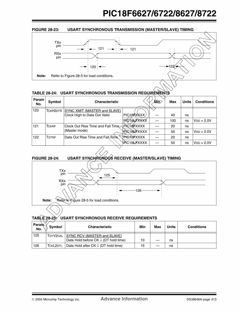
2004 Microchip Technology Inc. Advance Information DS39646A-page 413
PIC18F6627/6722/8627/8722
FIGURE 28-23: USART SYNCHRONOUS TRANSMISSION (MASTER/SLAVE) TIMING
TABLE 28-24: USART SYNCHRONOUS TRANSMISSION REQUIREMENTS
FIGURE 28-24: USART SYNCHRONOUS RECEIVE (MASTER/SLAVE) TIMING
TABLE 28-25: USART SYNCHRONOUS RECEIVE REQUIREMENTS
121 121
120 122
TXx
RXxpin
pin
Note: Refer to Figure 28-5 for load conditions.
Param No.
Symbol Characteristic Min Max Units Conditions
120 TCKH2DTV SYNC XMIT (MASTER and SLAVE)Clock High to Data Out Valid PIC18FXXXX — 40 ns
PIC18LFXXXX — 100 ns VDD = 2.0V
121 TCKRF Clock Out Rise Time and Fall Time (Master mode)
PIC18FXXXX — 20 ns
PIC18LFXXXX — 50 ns VDD = 2.0V
122 TDTRF Data Out Rise Time and Fall Time PIC18FXXXX — 20 ns
PIC18LFXXXX — 50 ns VDD = 2.0V
125
126
TXx
RXx
pin
pin
Note: Refer to Figure 28-5 for load conditions.
Param. No.
Symbol Characteristic Min Max Units Conditions
125 TDTV2CKL SYNC RCV (MASTER and SLAVE)Data Hold before CK ↓ (DT hold time) 10 — ns
126 TCKL2DTL Data Hold after CK ↓ (DT hold time) 15 — ns

PIC18F6627/6722/8627/8722
DS39646A-page 414 Advance Information 2004 Microchip Technology Inc.
TABLE 28-26: A/D CONVERTER CHARACTERISTICS: PIC18F6627/6722/8627/8722 (INDUSTRIAL)PIC18LF6627/6722/8627/8722 (INDUSTRIAL)
FIGURE 28-25: A/D CONVERSION TIMING
Param No.
Symbol Characteristic Min Typ Max Units Conditions
A01 NR Resolution — — 10 bit ∆VREF ≥ 3.0V
A03 EIL Integral Linearity Error — — <±1 LSb ∆VREF ≥ 3.0V
A04 EDL Differential Linearity Error — — <±1 LSb ∆VREF ≥ 3.0V
A06 EOFF Offset Error — — <±1.5 LSb ∆VREF ≥ 3.0V
A07 EGN Gain Error — — <±1 LSb ∆VREF ≥ 3.0V
A10 — Monotonicity Guaranteed(1) — VSS ≤ VAIN ≤ VREF
A20 ∆VREF Reference Voltage Range(VREFH – VREFL)
1.83
——
——
VV
VDD < 3.0VVDD ≥ 3.0V
A21 VREFH Reference Voltage High VSS — VREFH V
A22 VREFL Reference Voltage Low VSS – 0.3V — VDD – 3.0V V
A25 VAIN Analog Input Voltage VREFL — VREFH V
A30 ZAIN Recommended Impedance of Analog Voltage Source
— — 2.5 kΩ
A50 IREF VREF Input Current(2) ——
——
5150
µAµA
During VAIN acquisition.During A/D conversion cycle.
Note 1: The A/D conversion result never decreases with an increase in the input voltage and has no missing codes.2: VREFH current is from RA3/AN3/VREF+ pin or VDD, whichever is selected as the VREFH source.
VREFL current is from RA2/AN2/VREF- pin or VSS, whichever is selected as the VREFL source.
131
130
132
BSF ADCON0, GO
Q4
A/D CLK
A/D DATA
ADRES
ADIF
GO
SAMPLE
OLD_DATA
SAMPLING STOPPED
DONE
NEW_DATA
(Note 1, 2)
9 8 7 2 1 0
Note 1: If the A/D clock source is selected as RC, a time of TCY is added before the A/D clock starts. This allows the SLEEP instruction to be executed.
2: This is a minimal RC delay (typically 100 ns), which also disconnects the holding capacitor from the analog input.
. . . . . .
TCY

2004 Microchip Technology Inc. Advance Information DS39646A-page 415
PIC18F6627/6722/8627/8722
TABLE 28-27: A/D CONVERSION REQUIREMENTS
Param No.
Symbol Characteristic Min Max Units Conditions
130 TAD A/D Clock Period PIC18FXXXX 0.7 25.0(1) µs TOSC based, VREF ≥ 3.0V
PIC18LFXXXX 1.4 25.0(1) µs VDD = 2.0V;TOSC based, VREF full range
PIC18FXXXX TBD 1 µs A/D RC mode
PIC18LFXXXX TBD 3 µs VDD = 2.0V; A/D RC mode
131 TCNV Conversion Time (not including acquisition time) (Note 2)
11 12 TAD
132 TACQ Acquisition Time (Note 3) 1.4TBD
——
µsµs
-40°C to +85°C 0°C ≤ to ≤ +85°C
135 TSWC Switching Time from Convert → Sample — (Note 4)
137 TDIS Discharge Time 0.2 — µs
Legend: TBD = To Be Determined
Note 1: The time of the A/D clock period is dependent on the device frequency and the TAD clock divider. 2: ADRES register may be read on the following TCY cycle.3: The time for the holding capacitor to acquire the “New” input voltage when the voltage changes full scale
after the conversion (VDD to VSS or VSS to VDD). The source impedance (RS) on the input channels is 50Ω.4: On the following cycle of the device clock.

PIC18F6627/6722/8627/8722
DS39646A-page 416 Advance Information 2004 Microchip Technology Inc.
NOTES:

2004 Microchip Technology Inc. Advance Information DS39646A-page 417
PIC18F6627/6722/8627/8722
29.0 DC AND AC CHARACTERISTICS GRAPHS AND TABLES
Graphs and tables are not available at this time.

PIC18F6627/6722/8627/8722
DS39646A-page 418 Advance Information 2004 Microchip Technology Inc.
NOTES:
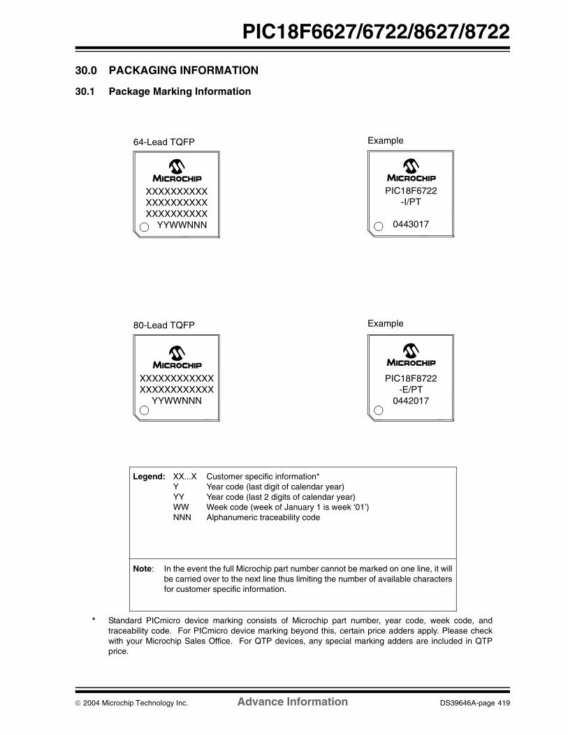
2004 Microchip Technology Inc. Advance Information DS39646A-page 419
PIC18F6627/6722/8627/8722
30.0 PACKAGING INFORMATION
30.1 Package Marking Information
80-Lead TQFP Example
64-Lead TQFP Example
XXXXXXXXXXXXXXXXXXXXXXXX
YYWWNNN
XXXXXXXXXXXXXXXXXXXXXXXXXXXXXX YYWWNNN
PIC18F6722-I/PT
0443017
PIC18F8722-E/PT
0442017
Legend: XX...X Customer specific information*Y Year code (last digit of calendar year)YY Year code (last 2 digits of calendar year)WW Week code (week of January 1 is week ‘01’)NNN Alphanumeric traceability code
Note: In the event the full Microchip part number cannot be marked on one line, it willbe carried over to the next line thus limiting the number of available charactersfor customer specific information.
* Standard PICmicro device marking consists of Microchip part number, year code, week code, andtraceability code. For PICmicro device marking beyond this, certain price adders apply. Please checkwith your Microchip Sales Office. For QTP devices, any special marking adders are included in QTPprice.

PIC18F6627/6722/8627/8722
DS39646A-page 420 Advance Information 2004 Microchip Technology Inc.
30.2 Package Details
The following sections give the technical details of thepackages.
64-Lead Plastic Thin Quad Flatpack (PT) 10x10x1 mm Body, 1.0/0.10 mm Lead Form (TQFP)
* Controlling Parameter
Notes:Dimensions D1 and E1 do not include mold flash or protrusions. Mold flash or protrusions shall not exceed.010” (0.254mm) per side.JEDEC Equivalent: MS-026Drawing No. C04-085
1510515105βMold Draft Angle Bottom1510515105αMold Draft Angle Top
0.270.220.17.011.009.007BLead Width0.230.180.13.009.007.005cLead Thickness
1616n1Pins per Side
10.1010.009.90.398.394.390D1Molded Package Length10.1010.009.90.398.394.390E1Molded Package Width12.2512.0011.75.482.472.463DOverall Length12.2512.0011.75.482.472.463EOverall Width
73.5073.50φFoot Angle
0.750.600.45.030.024.018LFoot Length0.250.150.05.010.006.002A1Standoff §1.051.000.95.041.039.037A2Molded Package Thickness1.201.101.00.047.043.039AOverall Height
0.50.020pPitch6464nNumber of Pins
MAXNOMMINMAXNOMMINDimension LimitsMILLIMETERS*INCHESUnits
c
21
n
DD1
B
p
#leads=n1
E1
E
A2
A1
A
L
CH x 45°
βφ
α
(F)
Footprint (Reference) (F) .039 1.00
Pin 1 Corner Chamfer CH .025 .035 .045 0.64 0.89 1.14
§ Significant Characteristic

2004 Microchip Technology Inc. Advance Information DS39646A-page 421
PIC18F6627/6722/8627/8722
80-Lead Plastic Thin Quad Flatpack (PT) 12x12x1 mm Body, 1.0/0.10 mm Lead Form (TQFP)
* Controlling Parameter
Notes:Dimensions D1 and E1 do not include mold flash or protrusions. Mold flash or protrusions shall not exceed .010” (0.254mm) per side.JEDEC Equivalent: MS-026Drawing No. C04-092
1.101.00.043.039
1.140.890.64.045.035.025CHPin 1 Corner Chamfer
1.00.039(F)Footprint (Reference)
(F)
EE1
#leads=n1
p
B
D1 D
n
12
φ
c
βL
A
A1A2
α
Units INCHES MILLIMETERS*Dimension Limits MIN NOM MAX MIN NOM MAX
Number of Pins n 80 80Pitch p .020 0.50
Overall Height A .047 1.20Molded Package Thickness A2 .037 .039 .041 0.95 1.00 1.05Standoff § A1 .002 .004 .006 0.05 0.10 0.15Foot Length L .018 .024 .030 0.45 0.60 0.75
Foot Angle φ 0 3.5 7 0 3.5 7Overall Width E .541 .551 .561 13.75 14.00 14.25Overall Length D .541 .551 .561 13.75 14.00 14.25Molded Package Width E1 .463 .472 .482 11.75 12.00 12.25Molded Package Length D1 .463 .472 .482 11.75 12.00 12.25
Pins per Side n1 20 20
Lead Thickness c .004 .006 .008 0.09 0.15 0.20Lead Width B .007 .009 .011 0.17 0.22 0.27
Mold Draft Angle Top α 5 10 15 5 10 15Mold Draft Angle Bottom β 5 10 15 5 10 15
CH x 45°
§ Significant Characteristic

PIC18F6627/6722/8627/8722
DS39646A-page 422 Advance Information 2004 Microchip Technology Inc.
NOTES:

2004 Microchip Technology Inc. Advance Information DS39646A-page 423
PIC18F6627/6722/8627/8722
APPENDIX A: REVISION HISTORY
Revision A (September 2004)
Original data sheet for PIC18F6627/6722/8627/8722devices.
APPENDIX B: DEVICE DIFFERENCES
The differences between the devices listed in this datasheet are shown in Table B-1.
TABLE B-1: DEVICE DIFFERENCES
Features PIC18F6627 PIC18F6722 PIC18F8627 PIC18F8722
Program Memory (Bytes) 96K 128K 96K 128K
Program Memory (Instructions) 49152 65536 49152 65536
Interrupt Sources 28 28 29 29
I/O Ports Ports A, B, C, D, E, F, G
Ports A, B, C, D, E, F, G
Ports A, B, C, D, E, F, G, H, J
Ports A, B, C, D, E, F, G, H, J
Capture/Compare/PWM Modules 2 2 2 2
Enhanced Capture/Compare/PWM Modules
3 3 3 3
Parallel Communications (PSP) Yes Yes Yes Yes
External Memory Bus No No Yes Yes
10-bit Analog-to-Digital Module 12 input channels 12 input channels 16 input channels 16 input channels
Packages 64-pin TQFP 64-pin TQFP 80-pin TQFP 80-pin TQFP

PIC18F6627/6722/8627/8722
DS39646A-page 424 Advance Information 2004 Microchip Technology Inc.
APPENDIX C: CONVERSION CONSIDERATIONS
This appendix discusses the considerations forconverting from previous versions of a device to theones listed in this data sheet. Typically, these changesare due to the differences in the process technologyused. An example of this type of conversion is from aPIC16C74A to a PIC16C74B.
Not Applicable
APPENDIX D: MIGRATION FROM BASELINE TO ENHANCED DEVICES
This section discusses how to migrate from a Baselinedevice (i.e., PIC16C5X) to an Enhanced MCU device(i.e., PIC18FXXX).
The following are the list of modifications over thePIC16C5X microcontroller family:
Not Currently Available

2004 Microchip Technology Inc. Advance Information DS39646A-page 425
PIC18F6627/6722/8627/8722
APPENDIX E: MIGRATION FROM MID-RANGE TO ENHANCED DEVICES
A detailed discussion of the differences between themid-range MCU devices (i.e., PIC16CXXX) and theenhanced devices (i.e., PIC18FXXX) is provided inAN716, “Migrating Designs from PIC16C74A/74B toPIC18C442”. The changes discussed, while devicespecific, are generally applicable to all mid-range toenhanced device migrations.
This Application Note is available on our web site,www.micorochip.com, as Literature Number DS00716.
APPENDIX F: MIGRATION FROM HIGH-END TO ENHANCED DEVICES
A detailed discussion of the migration pathway anddifferences between the high-end MCU devices (i.e., PIC17CXXX) and the enhanced devices (i.e., PIC18FXXX) is provided in AN726, “PIC17CXXXto PIC18CXXX Migration”. This Application Note isavailable on our web site, www.micorochip.com, asLiterature Number DS00726.

PIC18F6627/6722/8627/8722
DS39646A-page 426 Advance Information 2004 Microchip Technology Inc.
NOTES:

2004 Microchip Technology Inc. Advance Information DS39646A-page 427
PIC18F6627/6722/8627/8722
INDEX
AA/D ................................................................................... 269
A/D Converter Interrupt, Configuring ....................... 273Acquisition Requirements ........................................ 274ADCON0 Register .................................................... 269ADCON1 Register .................................................... 269ADCON2 Register .................................................... 269ADRESH Register ............................................ 269, 272ADRESL Register .................................................... 269Analog Port Pins ...................................................... 158Analog Port Pins, Configuring .................................. 276Associated Registers ............................................... 278Calculating the Minimum Required
Acquisition Time .............................................. 274Configuring the Module ............................................ 273Conversion Clock (TAD) ........................................... 275Conversion Status (GO/DONE Bit) .......................... 272Conversions ............................................................. 277Converter Characteristics ........................................ 414Discharge ................................................................. 277Operation in Power Managed Modes ...................... 276Selecting and Configuring Acquisition Time ............ 275Special Event Trigger (CCP) .................................... 278Special Event Trigger (ECCP) ................................. 192Use of the CCP2 Trigger .......................................... 278
Absolute Maximum Ratings ............................................. 373AC (Timing) Characteristics ............................................. 394
Load Conditions for Device Timing Specifications ... 395Parameter Symbology ............................................. 394Temperature and Voltage Specifications ................. 395Timing Conditions .................................................... 395
Access BankMapping with Indexed Literal Offset Mode ................. 84
ACKSTAT ........................................................................ 236ACKSTAT Status Flag ..................................................... 236ADCON0 Register ............................................................ 269
GO/DONE Bit ........................................................... 272ADCON1 Register ............................................................ 269ADCON2 Register ............................................................ 269ADDFSR .......................................................................... 360ADDLW ............................................................................ 323ADDULNK ........................................................................ 360ADDWF ............................................................................ 323ADDWFC ......................................................................... 324ADRESH Register ............................................................ 269ADRESL Register .................................................... 269, 272Analog-to-Digital Converter. See A/D.ANDLW ............................................................................ 324ANDWF ............................................................................ 325Assembler
MPASM Assembler .................................................. 367Auto-Wake-up on Sync Break Character ......................... 261
BBank Select Register (BSR) ............................................... 71Baud Rate Generator ....................................................... 232BC .................................................................................... 325BCF .................................................................................. 326BF .................................................................................... 236BF Status Flag ................................................................. 236Block Diagrams
16-bit Byte Select Mode ........................................... 10116-bit Byte Write Mode .............................................. 99
16-bit Word Write Mode ........................................... 100A/D ........................................................................... 272Analog Input Model .................................................. 273Baud Rate Generator .............................................. 232Capture Mode Operation ......................................... 181Comparator Analog Input Model .............................. 283Comparator I/O Operating Modes ........................... 280Comparator Output .................................................. 282Comparator Voltage Reference ............................... 286Compare Mode Operation ....................................... 182Device Clock .............................................................. 37Enhanced PWM ....................................................... 193EUSART Receive .................................................... 260EUSART Transmit ................................................... 258External Power-on Reset Circuit
(Slow VDD Power-up) ........................................ 51Fail-Safe Clock Monitor (FSCM) .............................. 311Generic I/O Port Operation ...................................... 133High/Low-Voltage Detect with External Input .......... 290Interrupt Logic .......................................................... 118MSSP (I2C Master Mode) ........................................ 230MSSP (I2C Mode) .................................................... 215MSSP (SPI Mode) ................................................... 205On-Chip Reset Circuit ................................................ 49PIC18F6627/6722 ..................................................... 10PIC18F8627/8722 ..................................................... 11PLL (HS Mode) .................................................... 33, 34PORTD and PORTE (Parallel Slave Port) ............... 158PWM Operation (Simplified) .................................... 184Reads from Flash Program Memory ......................... 89Single Comparator ................................................... 281Table Read Operation ............................................... 85Table Write Operation ............................................... 86Table Writes to Flash Program Memory .................... 91Timer0 in 16-Bit Mode ............................................. 162Timer0 in 8-Bit Mode ............................................... 162Timer1 ..................................................................... 166Timer1 (16-Bit Read/Write Mode) ............................ 166Timer2 ..................................................................... 172Timer3 ..................................................................... 174Timer3 (16-Bit Read/Write Mode) ............................ 174Timer4 ..................................................................... 178Voltage Reference Output Buffer Example ............. 287Watchdog Timer ...................................................... 308
BN .................................................................................... 326BNC ................................................................................. 327BNN ................................................................................. 327BNOV .............................................................................. 328BNZ ................................................................................. 328BOR. See Brown-out Reset.BOV ................................................................................. 331BRA ................................................................................. 329Break Character (12-Bit) Transmit and Receive .............. 263BRG. See Baud Rate Generator.Brown-out Reset (BOR) ..................................................... 52
Detecting ................................................................... 52Disabling in Sleep Mode ............................................ 52Software Enabled ...................................................... 52
BSF .................................................................................. 329BTFSC ............................................................................. 330BTFSS ............................................................................. 330BTG ................................................................................. 331BZ .................................................................................... 332

PIC18F6627/6722/8627/8722
DS39646A-page 428 Advance Information 2004 Microchip Technology Inc.
CC Compilers
MPLAB C17 ............................................................. 368MPLAB C18 ............................................................. 368MPLAB C30 ............................................................. 368
CALL ................................................................................ 332CALLW ............................................................................. 361Capture (CCP Module) ..................................................... 181
Associated Registers ............................................... 183CCP Pin Configuration ............................................. 181CCPRxH:CCPRxL Registers ................................... 181Prescaler .................................................................. 181Software Interrupt .................................................... 181Timer1/Timer3 Mode Selection ................................ 181
Capture (ECCP Module) .................................................. 192Capture/Compare/PWM (CCP) ........................................ 179
Capture Mode. See Capture.CCP Mode and Timer Resources ............................ 180CCPRxH Register .................................................... 180CCPRxL Register ..................................................... 180Compare Mode. See Compare.Interconnect Configurations ..................................... 180Module Configuration ............................................... 180
Clock Sources .................................................................... 37Selecting the 31 kHz Source ...................................... 38Selection Using OSCCON Register ........................... 38
CLRF ................................................................................ 333CLRWDT .......................................................................... 333Code Examples
16 x 16 Signed Multiply Routine .............................. 11616 x 16 Unsigned Multiply Routine .......................... 1168 x 8 Signed Multiply Routine .................................. 1158 x 8 Unsigned Multiply Routine .............................. 115Changing Between Capture Prescalers ................... 181Computed GOTO Using an Offset Value ................... 68Data EEPROM Read ............................................... 111Data EEPROM Refresh Routine .............................. 112Data EEPROM Write ............................................... 111Erasing a Flash Program Memory Row ..................... 90Fast Register Stack .................................................... 68How to Clear RAM (Bank 1) Using Indirect
Addressing ......................................................... 80Implementing a Real-Time Clock Using a Timer1
Interrupt Service ............................................... 169Initializing PORTA .................................................... 133Initializing PORTB .................................................... 136Initializing PORTC .................................................... 139Initializing PORTD .................................................... 142Initializing PORTE .................................................... 145Initializing PORTF .................................................... 148Initializing PORTG ................................................... 150Initializing PORTH .................................................... 153Initializing PORTJ .................................................... 156Loading the SSPxBUF (SSPSR) Register ............... 208Reading a Flash Program Memory Word .................. 89Saving Status, WREG and BSR Registers
in RAM ............................................................. 132Writing to Flash Program Memory ....................... 92–93
Code Protection ............................................................... 295COMF ............................................................................... 334Comparator ...................................................................... 279
Analog Input Connection Considerations ................. 283Associated Registers ............................................... 283Configuration ............................................................ 280Effects of a Reset ..................................................... 282
Interrupts ................................................................. 282Operation ................................................................. 281Operation During Sleep ........................................... 282Outputs .................................................................... 281Reference ................................................................ 281
External Signal ................................................ 281Internal Signal .................................................. 281
Response Time ........................................................ 281Comparator Specifications ............................................... 392Comparator Voltage Reference ....................................... 285
Accuracy and Error .................................................. 286Associated Registers ............................................... 287Configuring .............................................................. 285Connection Considerations ...................................... 286Effects of a Reset .................................................... 286Operation During Sleep ........................................... 286
Compare (CCP Module) .................................................. 182Associated Registers ............................................... 183CCPRx Register ...................................................... 182Pin Configuration ..................................................... 182Software Interrupt .................................................... 182Special Event Trigger .............................. 175, 182, 278Timer1/Timer3 Mode Selection ................................ 182
Compare (ECCP Module) ................................................ 192Special Event Trigger .............................................. 192
Computed GOTO ............................................................... 68Configuration Bits ............................................................ 295Configuration Register Protection .................................... 316Context Saving During Interrupts ..................................... 132Conversion Considerations .............................................. 424CPFSEQ .......................................................................... 334CPFSGT .......................................................................... 335CPFSLT ........................................................................... 335Crystal Oscillator/Ceramic Resonator ................................ 31
DData Addressing Modes .................................................... 80
Comparing Addressing Modes with the Extended Instruction Set Enabled ..................... 83
Direct ......................................................................... 80Indexed Literal Offset ................................................ 82
Instructions Affected .......................................... 82Indirect ....................................................................... 80Inherent and Literal .................................................... 80
Data EEPROMCode Protection ....................................................... 316
Data EEPROM Memory ................................................... 109Associated Registers ............................................... 113EEADR and EEADRH Registers ............................. 109EECON1 and EECON2 Registers ........................... 109Operation During Code-Protect ............................... 112Protection Against Spurious Write ........................... 112Reading ................................................................... 111Using ....................................................................... 112Write Verify .............................................................. 111Writing ..................................................................... 111
Data Memory ..................................................................... 71Access Bank .............................................................. 73and the Extended Instruction Set .............................. 82Bank Select Register (BSR) ...................................... 71General Purpose Registers ....................................... 73Map for PIC18F6627/8627 ........................................ 72Special Function Registers ........................................ 74
DAW ................................................................................ 336DC and AC Characteristics
Graphs and Tables .................................................. 417
2004 Microchip Technology Inc. Advance Information DS39646A-page 429
PIC18F6627/6722/8627/8722
DC Characteristics ........................................................... 389Power-Down and Supply Current ............................ 377Supply Voltage ......................................................... 376
DCFSNZ .......................................................................... 337DECF ............................................................................... 336DECFSZ ........................................................................... 337Demonstration Boards
PICDEM 1 ................................................................ 370PICDEM 17 .............................................................. 371PICDEM 18R ........................................................... 371PICDEM 2 Plus ........................................................ 370PICDEM 3 ................................................................ 370PICDEM 4 ................................................................ 370PICDEM LIN ............................................................ 371PICDEM USB ........................................................... 371PICDEM.net Internet/Ethernet ................................. 370
Development Support ...................................................... 367Device Differences ........................................................... 423Device Overview .................................................................. 7
Details on Individual Family Members ......................... 8Features (table) ............................................................ 9New Core Features ...................................................... 7
Device Reset Timers .......................................................... 53Oscillator Start-up Timer (OST) ................................. 53PLL Lock Time-out ..................................................... 53Power-up Timer (PWRT) ........................................... 53Time-out Sequence .................................................... 53
Direct Addressing ............................................................... 81
EECCP
Capture and Compare Modes .................................. 192Standard PWM Mode ............................................... 192
Effect on Standard PIC Instructions ................................. 364Effects of Power Managed Modes on Various
Clock Sources ............................................................ 40Electrical Characteristics .................................................. 373Enhanced Capture/Compare/PWM (ECCP) .................... 187
and Program Memory modes .................................. 188Capture Mode. See Capture (ECCP Module).Outputs and Configuration ....................................... 188Pin Configurations for ECCP1 ................................. 189Pin Configurations for ECCP2 ................................. 190Pin Configurations for ECCP3 ................................. 191PWM Mode. See PWM (ECCP Module).Timer Resources ...................................................... 191
Enhanced PWM Mode. See PWM (ECCP Module). ........ 192Enhanced Universal Synchronous Asynchronous
Receiver Transmitter (EUSART). See EUSART.Equations
A/D Acquisition Time ................................................ 274A/D Minimum Charging Time ................................... 274
Errata ................................................................................... 5EUSART
Asynchronous Mode ................................................ 25712-bit Break Transmit and Receive ................. 263Associated Registers, Receive ........................ 261Associated Registers, Transmit ....................... 259Auto-Wake-up on Sync Break ......................... 261Receiver ........................................................... 260Setting up 9-Bit Mode with Address Detect ..... 260Transmitter ....................................................... 257
Baud Rate GeneratorOperation in Power Managed Mode ................ 251
Baud Rate Generator (BRG) .................................... 251Associated Registers ....................................... 252Auto-Baud Rate Detect .................................... 255
Baud Rate Error, Calculating ........................... 252Baud Rates, Asynchronous Modes ................. 253High Baud Rate Select (BRGH Bit) ................. 251Sampling ......................................................... 251
Synchronous Master Mode ...................................... 264Associated Registers, Receive ........................ 266Associated Registers, Transmit ....................... 265Reception ........................................................ 266Transmission ................................................... 264
Synchronous Slave Mode ........................................ 267Associated Registers, Receive ........................ 268Associated Registers, Transmit ....................... 267Reception ........................................................ 268Transmission ................................................... 267
Evaluation and Programming Tools ................................. 371Extended Instruction Set
ADDFSR .................................................................. 360ADDULNK ............................................................... 360and Using MPLAB Tools ......................................... 366CALLW .................................................................... 361Considerations for Use ............................................ 364MOVSF .................................................................... 361MOVSS .................................................................... 362PUSHL ..................................................................... 362SUBFSR .................................................................. 363SUBULNK ................................................................ 363Syntax ...................................................................... 359
Extended Microcontroller Mode ......................................... 98External Clock Input ........................................................... 32External Memory Bus ........................................................ 95External Memory Interface
16-bit Byte Select Mode .......................................... 10116-bit Byte Write Mode .............................................. 9916-bit Mode ........................................................ 98, 10416-bit Mode Timing .......................................... 102, 10516-bit Word Write Mode ........................................... 100PIC18F8410 External Bus - I/O Port Functions ......... 95
FFail-Safe Clock Monitor ........................................... 295, 311
Exiting Operation ..................................................... 311Interrupts in Power Managed Modes ....................... 312POR or Wake from Sleep ........................................ 312WDT During Oscillator Failure ................................. 311
Fast Register Stack ........................................................... 68Firmware Instructions ...................................................... 317Flash Program Memory ..................................................... 85
Associated Registers ................................................. 93Control Registers ....................................................... 86
EECON1 and EECON2 ..................................... 86TABLAT (Table Latch) Register ........................ 88TBLPTR (Table Pointer) Register ...................... 88
Erase Sequence ........................................................ 90Erasing ...................................................................... 90Operation During Code-Protect ................................. 93Reading ..................................................................... 89Table Pointer
Boundaries Based on Operation ....................... 88Table Pointer Boundaries .......................................... 88Table Reads and Table Writes .................................. 85Write Sequence ......................................................... 91Writing To .................................................................. 91
Protection Against Spurious Writes ................... 93Unexpected Termination ................................... 93Write Verify ........................................................ 93
FSCM. See Fail-Safe Clock Monitor.

PIC18F6627/6722/8627/8722
DS39646A-page 430 Advance Information 2004 Microchip Technology Inc.
GGeneral Call Address Support ......................................... 229GOTO ............................................................................... 338
HHardware Multiplier .......................................................... 115
Introduction .............................................................. 115Operation ................................................................. 115Performance Comparison ........................................ 115
High/Low-Voltage Detect ................................................. 289Applications .............................................................. 292Associated Registers ............................................... 293Characteristics ......................................................... 393Current Consumption ............................................... 291Effects of a Reset ..................................................... 293Operation ................................................................. 290
During Sleep .................................................... 293Setup ........................................................................ 291Start-up Time ........................................................... 291Typical Application ................................................... 292
HLVD. See High/Low-Voltage Detect. ............................. 289
II/O Ports ........................................................................... 133I2C Mode (MSSP)
Acknowledge Sequence Timing ............................... 239Associated Registers ............................................... 245Baud Rate Generator ............................................... 232Bus Collision
During a Repeated Start Condition .................. 243During a Stop Condition ................................... 244
Clock Arbitration ....................................................... 233Clock Stretching ....................................................... 225
10-Bit Slave Receive Mode (SEN = 1) ............. 22510-Bit Slave Transmit Mode ............................. 2257-Bit Slave Receive Mode (SEN = 1) ............... 2257-Bit Slave Transmit Mode ............................... 225
Clock Synchronization and the CKP bit (SEN = 1) .. 226Effects of a Reset ..................................................... 240General Call Address Support ................................. 229I2C Clock Rate w/BRG ............................................. 232Master Mode ............................................................ 230
Operation ......................................................... 231Reception ......................................................... 236Repeated Start Condition Timing ..................... 235Start Condition Timing ..................................... 234Transmission .................................................... 236
Multi-Master Communication, Bus Collision and Arbitration ......................................................... 240
Multi-Master Mode ................................................... 240Operation ................................................................. 219Read/Write Bit Information (R/W Bit) ............... 219, 220Registers .................................................................. 215Serial Clock (RC3/SCK/SCL) ................................... 220Slave Mode .............................................................. 219
Addressing ....................................................... 219Reception ......................................................... 220Transmission .................................................... 220
Sleep Operation ....................................................... 240Stop Condition Timing .............................................. 239
ID Locations ............................................................. 295, 316INCF ................................................................................. 338INCFSZ ............................................................................ 339In-Circuit Debugger .......................................................... 316In-Circuit Serial Programming (ICSP) ...................... 295, 316
Indexed Literal Offset Addressingand Standard PIC18 Instructions ............................. 364
Indexed Literal Offset Mode ............................................. 364Indirect Addressing ............................................................ 81INFSNZ ............................................................................ 339Initialization Conditions for all Registers ...................... 57–61Instruction Cycle ................................................................ 69
Clocking Scheme ....................................................... 69Instruction Flow/Pipelining ................................................. 69Instruction Set .................................................................. 317
ADDLW .................................................................... 323ADDWF .................................................................... 323ADDWF (Indexed Literal Offset Mode) .................... 365ADDWFC ................................................................. 324ANDLW .................................................................... 324ANDWF .................................................................... 325BC ............................................................................ 325BCF ......................................................................... 326BN ............................................................................ 326BNC ......................................................................... 327BNN ......................................................................... 327BNOV ...................................................................... 328BNZ ......................................................................... 328BOV ......................................................................... 331BRA ......................................................................... 329BSF .......................................................................... 329BSF (Indexed Literal Offset Mode) .......................... 365BTFSC ..................................................................... 330BTFSS ..................................................................... 330BTG ......................................................................... 331BZ ............................................................................ 332CALL ........................................................................ 332CLRF ....................................................................... 333CLRWDT ................................................................. 333COMF ...................................................................... 334CPFSEQ .................................................................. 334CPFSGT .................................................................. 335CPFSLT ................................................................... 335DAW ........................................................................ 336DCFSNZ .................................................................. 337DECF ....................................................................... 336DECFSZ .................................................................. 337Extended Instruction Set ......................................... 359General Format ........................................................ 319GOTO ...................................................................... 338INCF ........................................................................ 338INCFSZ .................................................................... 339INFSNZ .................................................................... 339IORLW ..................................................................... 340IORWF ..................................................................... 340LFSR ....................................................................... 341MOVF ...................................................................... 341MOVFF .................................................................... 342MOVLB .................................................................... 342MOVLW ................................................................... 343MOVWF ................................................................... 343MULLW .................................................................... 344MULWF .................................................................... 344NEGF ....................................................................... 345NOP ......................................................................... 345Opcode Field Descriptions ....................................... 318POP ......................................................................... 346PUSH ....................................................................... 346RCALL ..................................................................... 347RESET ..................................................................... 347

2004 Microchip Technology Inc. Advance Information DS39646A-page 431
PIC18F6627/6722/8627/8722
RETFIE .................................................................... 348RETLW .................................................................... 348RETURN .................................................................. 349RLCF ........................................................................ 349RLNCF ..................................................................... 350RRCF ....................................................................... 350RRNCF .................................................................... 351SETF ........................................................................ 351SETF (Indexed Literal Offset Mode) ........................ 365SLEEP ..................................................................... 352SUBFWB .................................................................. 352SUBLW .................................................................... 353SUBWF .................................................................... 353SUBWFB .................................................................. 354SWAPF .................................................................... 354TBLRD ..................................................................... 355TBLWT ..................................................................... 356TSTFSZ ................................................................... 357XORLW .................................................................... 357XORWF .................................................................... 358
INTCON RegisterRBIF Bit .................................................................... 136
INTCON Registers ........................................................... 119Inter-Integrated Circuit. See I2C.Internal Oscillator Block ..................................................... 34
Adjustment ................................................................. 34INTIO Modes .............................................................. 34INTOSC Frequency Drift ............................................ 35INTOSC Output Frequency ........................................ 34OSCTUNE Register ................................................... 34PLL in INTOSC Modes .............................................. 35
Internal RC OscillatorUse with WDT .......................................................... 308
Interrupt Sources ............................................................. 295A/D Conversion Complete ....................................... 273Capture Complete (CCP) ......................................... 181Compare Complete (CCP) ....................................... 182Interrupt-on-Change (RB7:RB4) .............................. 136INTn Pin ................................................................... 132PORTB, Interrupt-on-Change .................................. 132TMR0 ....................................................................... 132TMR0 Overflow ........................................................ 163TMR1 Overflow ........................................................ 165TMR2 to PR2 Match (PWM) ............................ 184, 192TMR3 Overflow ................................................ 173, 175TMR4 to PR4 Match ................................................ 178TMR4 to PR4 Match (PWM) .................................... 177
Interrupts .......................................................................... 117Interrupts, Flag Bits
Interrupt-on-Change (RB7:RB4) Flag (RBIF Bit) ..... 136INTOSC, INTRC. See Internal Oscillator Block.IORLW ............................................................................. 340IORWF ............................................................................. 340IPR Registers ................................................................... 128
KKey Features
Easy Migration ............................................................. 8Expanded Memory ....................................................... 7External Memory Interface ........................................... 8
LLFSR ................................................................................ 341Low-Voltage ICSP Programming. See Single-Supply
ICSP Programming
MMaster Clear (MCLR) ......................................................... 51Master Synchronous Serial Port (MSSP). See MSSP.Memory
Mode Memory Access ............................................... 64Memory Maps for PIC18F6X2X/8X2X Program
Memory Modes .......................................................... 65Memory Organization ........................................................ 63
Data Memory ............................................................. 71Program Memory ....................................................... 63
Modes ................................................................ 63Memory Programming Requirements .............................. 391Microcontroller Mode ......................................................... 98Microprocessor Mode ........................................................ 98Microprocessor with Boot Block Mode ............................... 98Migration from Baseline to Enhanced Devices ................ 424Migration from High-End to Enhanced Devices ............... 425Migration from Mid-Range to Enhanced Devices ............ 425MOVF .............................................................................. 341MOVFF ............................................................................ 342MOVLB ............................................................................ 342MOVLW ........................................................................... 343MOVSF ............................................................................ 361MOVSS ............................................................................ 362MOVWF ........................................................................... 343MPLAB ASM30 Assembler, Linker, Librarian .................. 368MPLAB ICD 2 In-Circuit Debugger .................................. 369MPLAB ICE 2000 High-Performance Universal
In-Circuit Emulator ................................................... 369MPLAB ICE 4000 High-Performance Universal
In-Circuit Emulator ................................................... 369MPLAB Integrated Development Environment Software . 367MPLAB PM3 Device Programmer ................................... 369MPLINK Object Linker/MPLIB Object Librarian ............... 368MSSP
ACK Pulse ....................................................... 219, 220Control Registers (general) ..................................... 205I2C Mode. See I2C Mode.Module Overview ..................................................... 205SPI Master/Slave Connection .................................. 209SPI Mode. See SPI Mode.SSPxBUF Register .................................................. 210SSPxSR Register .................................................... 210
MULLW ............................................................................ 344MULWF ............................................................................ 344
NNEGF ............................................................................... 345NOP ................................................................................. 345
OOscillator Configuration ..................................................... 31
EC .............................................................................. 31ECIO .......................................................................... 31HS .............................................................................. 31HSPLL ....................................................................... 31Internal Oscillator Block ............................................. 34INTIO1 ....................................................................... 31INTIO2 ....................................................................... 31LP .............................................................................. 31RC ............................................................................. 31RCIO .......................................................................... 31XT .............................................................................. 31
Oscillator Selection .......................................................... 295Oscillator Start-up Timer (OST) ................................... 40, 53

PIC18F6627/6722/8627/8722
DS39646A-page 432 Advance Information 2004 Microchip Technology Inc.
Oscillator Switching ............................................................ 37Oscillator Transitions .......................................................... 38Oscillator, Timer1 ..................................................... 165, 175Oscillator, Timer3 ............................................................. 173
PPackaging ........................................................................ 419
Details ...................................................................... 420Marking .................................................................... 419
Parallel Slave Port (PSP) ................................................. 158Associated Registers ............................................... 160RE0/RD Pin .............................................................. 158RE1/WR Pin ............................................................. 158RE2/CS Pin .............................................................. 158Select (PSPMODE Bit) ............................................ 158
PICkit 1 Flash Starter Kit .................................................. 371PICSTART Plus Development Programmer .................... 370PIE Registers ................................................................... 125Pin Functions
AVDD .......................................................................... 29AVDD .......................................................................... 19AVSS .......................................................................... 29AVSS .......................................................................... 19OSC1/CLKI/RA7 .................................................. 12, 20OSC2/CLKO/RA6 ................................................ 12, 20RA0/AN0 .............................................................. 13, 21RA1/AN1 .............................................................. 13, 21RA2/AN2/VREF- .................................................... 13, 21RA3/AN3/VREF+ ................................................... 13, 21RA4/T0CKI ........................................................... 13, 21RA5/AN4/HLVDIN ................................................ 13, 21RB0/INT0/FLT0 .................................................... 14, 22RB1/INT1 ............................................................. 14, 22RB2/INT2 ............................................................. 14, 22RB3/INT3 ................................................................... 14RB3/INT3/CCP2/P2A ................................................. 22RB4/KBI0 ............................................................. 14, 22RB5/KBI1/PGM .................................................... 14, 22RB6/KBI2/PGC .................................................... 14, 22RB7/KBI3/PGD .................................................... 14, 22RC0/T1OSO/T13CKI ........................................... 15, 23RC1/T1OSI/CCP2/P2A ........................................ 15, 23RC2/CCP1/P1A ................................................... 15, 23RC3/SCK1/SCL1 ................................................. 15, 23RC4/SDI1/SDA1 .................................................. 15, 23RC5/SDO1 ........................................................... 15, 23RC6/TX1/CK1 ...................................................... 15, 23RC7/RX1/DT1 ...................................................... 15, 23RD0/AD0/PSP0 .......................................................... 24RD0/PSP0 .................................................................. 16RD1/AD1/PSP1 .......................................................... 24RD1/PSP1 .................................................................. 16RD2/AD2/PSP2 .......................................................... 24RD2/PSP2 .................................................................. 16RD3/AD3/PSP3 .......................................................... 24RD3/PSP3 .................................................................. 16RD4/AD4/PSP4/SDO2 ............................................... 24RD4/PSP4/SDO2 ....................................................... 16RD5/AD5/PSP5/SDI2/SDA2 ...................................... 24RD5/PSP5/SDI2/SDA2 .............................................. 16RD6/AD6/PSP6/SCK2/SCL2 ..................................... 24RD6/PSP6/SCK2/SCL2 ............................................. 16RD7/AD7/PSP7/SS2 .................................................. 24RD7/PSP7/SS2 .......................................................... 16RE0/AD8/RD/P2D ...................................................... 25RE0/RD/P2D .............................................................. 17
RE1/AD9/WR/P2C ..................................................... 25RE1/WR/P2C ............................................................. 17RE2/AD10/CS/P2B .................................................... 25RE2/CS/P2D .............................................................. 17RE3/AD11/P3C .......................................................... 25RE3/P3C .................................................................... 17RE4/AD12/P3B .......................................................... 25RE4/P3B .................................................................... 17RE5/AD13/P1C .......................................................... 25RE5/P1C .................................................................... 17RE6/AD14/P1B .......................................................... 25RE6/P1B .................................................................... 17RE7/AD15/CCP2/P2A ............................................... 25RE7/CCP2/P2A ......................................................... 17RF0/AN5 .............................................................. 18, 26RF1/AN6/C2OUT ................................................. 18, 26RF2/AN7/C1OUT ................................................. 18, 26RF3/AN8 .............................................................. 18, 26RF4/AN9 .............................................................. 18, 26RF5/AN10/CVREF ................................................ 18, 26RF6/AN11 ............................................................ 18, 26RF7/SS1 .............................................................. 18, 26RG0/CCP3/P3A ................................................... 19, 27RG1/TX2/CK2 ...................................................... 19, 27RG2/RX2/DT2 ...................................................... 19, 27RG3/CCP4/P3D ................................................... 19, 27RG4/CCP5/P1D ................................................... 19, 27RG5 ..................................................................... 19, 27RG5/MCLR/VPP ................................................... 12, 20RH0/AD16 ................................................................. 28RH1/AD17 ................................................................. 28RH2/AD18 ................................................................. 28RH3/AD19 ................................................................. 28RH4/AN12/P3C .......................................................... 28RH5/AN13/P3B .......................................................... 28RH6/AN14/P1C .......................................................... 28RH7/AN15/P1B .......................................................... 28RJ0/ALE .................................................................... 29RJ1/OE ...................................................................... 29RJ2/WRL ................................................................... 29RJ3/WRH ................................................................... 29RJ4/BA0 .................................................................... 29RJ5/CE ...................................................................... 29RJ6/LB ....................................................................... 29RJ7/UB ...................................................................... 29VDD ............................................................................ 29VDD ............................................................................ 19VSS ............................................................................ 29VSS ............................................................................ 19
Pinout I/O DescriptionsPIC18F6627/6722 ..................................................... 12PIC18F8627/8722 ..................................................... 20
PIR Registers ................................................................... 122PLL Frequency Multiplier ................................................... 33
HSPLL Oscillator Mode ............................................. 33Use with INTOSC ...................................................... 33
POP ................................................................................. 346POR. See Power-on Reset.PORTA
Associated Registers ....................................... 107, 135Functions ................................................................. 134LATA Register ......................................................... 133PORTA Register ...................................................... 133TRISA Register ........................................................ 133
PORTB

2004 Microchip Technology Inc. Advance Information DS39646A-page 433
PIC18F6627/6722/8627/8722
Associated Registers ............................................... 138Functions ................................................................. 137LATB Register .......................................................... 136PORTB Register ...................................................... 136RB7:RB4 Interrupt-on-Change Flag (RBIF Bit) ........ 136TRISB Register ........................................................ 136
PORTCAssociated Registers ............................................... 141Functions ................................................................. 140LATC Register ......................................................... 139PORTC Register ...................................................... 139RC3/SCK/SCL Pin ................................................... 220TRISC Register ........................................................ 139
PORTD ............................................................................ 158Associated Registers ............................................... 144Functions ................................................................. 143LATD Register ......................................................... 142PORTD Register ...................................................... 142TRISD Register ........................................................ 142
PORTEAnalog Port Pins ...................................................... 158Associated Registers ............................................... 147Functions ................................................................. 146LATE Register .......................................................... 145PORTE Register ...................................................... 145PSP Mode Select (PSPMODE Bit) .......................... 158RE0/RD Pin .............................................................. 158RE1/WR Pin ............................................................. 158RE2/CS Pin .............................................................. 158TRISE Register ........................................................ 145
PORTFAssociated Registers ............................................... 149Functions ................................................................. 149LATF Register .......................................................... 148PORTF Register ...................................................... 148TRISF Register ........................................................ 148
PORTGAssociated Registers ............................................... 152Functions ................................................................. 151LATG Register ......................................................... 150PORTG Register ...................................................... 150TRISG Register ........................................................ 150
PORTHAssociated Registers ............................................... 155Functions ................................................................. 154LATH Register ......................................................... 153PORTH Register ...................................................... 153TRISH Register ........................................................ 153
PORTJAssociated Registers ............................................... 157Functions ................................................................. 157LATJ Register .......................................................... 156PORTJ Register ....................................................... 156TRISJ Register ......................................................... 156
Power Managed Modes ..................................................... 41and A/D Operation ................................................... 276and EUSART Operation ........................................... 251and Multiple Sleep Commands .................................. 42and PWM Operation ................................................ 203and SPI Operation ................................................... 213Clock Transitions and Status Indicators ..................... 42Effects on Clock Sources ........................................... 40Entering ...................................................................... 41Exiting Idle and Sleep Modes .................................... 47
by Interrupt ......................................................... 47
by Reset ............................................................ 47by WDT Time-out .............................................. 47Without a Start-up Delay ................................... 48
Idle Modes ................................................................. 45PRI_IDLE .......................................................... 46RC_IDLE ........................................................... 47SEC_IDLE ......................................................... 46
Run Modes ................................................................ 42PRI_RUN ........................................................... 42RC_RUN ............................................................ 43SEC_RUN ......................................................... 42
Selecting .................................................................... 41Sleep Mode ............................................................... 45Summary (table) ........................................................ 41
Power-on Reset (POR) ...................................................... 51Power-up Timer (PWRT) ........................................... 53Time-out Sequence ................................................... 53
Power-up Delays ............................................................... 40Power-up Timer (PWRT) ................................................... 40Prescaler
Timer2 ..................................................................... 193Prescaler, Timer0 ............................................................ 163Prescaler, Timer2 ............................................................ 185PRI_IDLE Mode ................................................................. 46PRI_RUN Mode ................................................................. 42PRO MATE II Universal Device Programmer .................. 369Program Counter ............................................................... 66
PCL, PCH and PCU Registers .................................. 66PCLATH and PCLATU Registers .............................. 66
Program Memoryand Extended Instruction Set .................................... 84Code Protection ....................................................... 314Extended Microcontroller Mode ................................. 63Instructions ................................................................ 70
Two-Word .......................................................... 70Interrupt Vector .......................................................... 63Look-up Tables .......................................................... 68Map and Stack (diagram) .......................................... 64Microcontroller Mode ................................................. 63Microprocessor Mode ................................................ 63Microprocessor with Boot Block Mode ...................... 63Reset Vector .............................................................. 63
Program Verification and Code Protection ...................... 313Associated Registers ............................................... 314
Programming, Device Instructions ................................... 317PSP.See Parallel Slave Port.Pulse Width Modulation. See PWM (CCP Module)
and PWM (ECCP Module).PUSH ............................................................................... 346PUSH and POP Instructions .............................................. 67PUSHL ............................................................................. 362PWM (CCP Module)
Associated Registers ............................................... 186CCPR1H:CCPR1L Registers .................................. 192Duty Cycle ....................................................... 184, 193Example Frequencies/Resolutions .................. 185, 193Period .............................................................. 184, 192Setup for PWM Operation ....................................... 185TMR2 to PR2 Match ........................................ 184, 192TMR4 to PR4 Match ................................................ 177
PWM (ECCP Module) ...................................................... 192Associated Registers ............................................... 204Direction Change in Full-Bridge Output Mode ......... 198Effects of a Reset .................................................... 203Enhanced PWM Auto-Shutdown ............................. 200

PIC18F6627/6722/8627/8722
DS39646A-page 434 Advance Information 2004 Microchip Technology Inc.
Full-Bridge Application Example .............................. 198Full-Bridge Mode ...................................................... 197Half-Bridge Mode ..................................................... 195Half-Bridge Output Mode Applications Example ...... 196Operation in Power Managed Modes ...................... 203Operation with Fail-Safe Clock Monitor ................... 203Output Configurations .............................................. 194Output Relationships (Active-High) .......................... 194Output Relationships (Active-Low) ........................... 195Programmable Dead-Band Delay ............................ 200Setup for PWM Operation ........................................ 203Start-up Considerations ........................................... 202
QQ Clock .................................................................... 185, 193
RRAM. See Data Memory.RC Oscillator ...................................................................... 33
RCIO Oscillator Mode ................................................ 33RC_IDLE Mode .................................................................. 47RC_RUN Mode .................................................................. 43RCALL .............................................................................. 347RCON Register
Bit Status During Initialization .................................... 56Register File ....................................................................... 73Registers
ADCON0 (A/D Control 0) ......................................... 269ADCON1 (A/D Control 1) ......................................... 270ADCON2 (A/D Control 2) ......................................... 271BAUDCONx (Baud Rate Control) ............................ 250CCPxCON (Capture/Compare/PWM Control) . 179, 187CMCON (Comparator Control) ................................ 279CONFIG1H (Configuration 1 High) .......................... 296CONFIG2H (Configuration 2 High) .................. 298, 299CONFIG2L (Configuration 2 Low) ............................ 297CONFIG3H (Configuration 3 High) .......................... 300CONFIG4L (Configuration 4 Low) ............................ 301CONFIG5H (Configuration 5 High) .......................... 303CONFIG5L (Configuration 5 Low) ............................ 302CONFIG6H (Configuration 6 High) .......................... 305CONFIG6L (Configuration 6 Low) ............................ 304CONFIG7H (Configuration 7 High) .......................... 307CONFIG7L (Configuration 7 Low) ............................ 306CVRCON (Comparator Voltage Reference Control) 285DEVID1 (Device ID 1) .............................................. 307DEVID2
(Device ID 2) .................................................... 307ECCPxAS (ECCP Auto-Shutdown Control) ............. 201ECCPxDEL (PWM Configuration) ............................ 200EECON1 (Data EEPROM Control 1) ................. 87, 110HLVDCON (High/Low-Voltage Detect Control) ........ 289INTCON (Interrupt Control) ...................................... 119INTCON2 (Interrupt Control 2) ................................. 120INTCON3 (Interrupt Control 3) ................................. 121IPR1 (Peripheral Interrupt Priority 1) ........................ 128IPR2 (Peripheral Interrupt Priority 2) ........................ 129IPR3 (Peripheral Interrupt Priority 3) ........................ 130MEMCON (External Memory Bus Control) ................ 96OSCCON (Oscillator Control) .................................... 39OSCTUNE (Oscillator Tuning) ................................... 35PIE1 (Peripheral Interrupt Enable 1) ........................ 125PIE2 (Peripheral Interrupt Enable 2) ........................ 126PIE3 (Peripheral Interrupt Enable 3) ........................ 127PIR1 (Peripheral Interrupt Request (Flag) 1) ........... 122PIR2 (Peripheral Interrupt Request (Flag) 2) ........... 123
PIR3 (Peripheral Interrupt Request (Flag) 3) ........... 124PSPCON (Parallel Slave Port Control) .................... 159RCON (Reset Control) ....................................... 50, 131RCSTAx (Receive Status and Control) .................... 249SSPxCON1 (MSSP Control 1, I2C Mode) ............... 217SSPxCON1 (MSSP Control 1, SPI Mode) ............... 207SSPxCON2 (MSSP Control 2, I2C Mode) ............... 218SSPxSTAT (MSSP Status, I2C Mode) ..................... 216SSPxSTAT (MSSP Status, SPI Mode) .................... 206Status ........................................................................ 79STKPTR (Stack Pointer) ............................................ 67T0CON (Timer0 Control) ......................................... 161T1CON (Timer1 Control) ......................................... 165T2CON (Timer2 Control) ......................................... 171T3CON (Timer3 Control) ......................................... 173T4CON (Timer 4 Control) ........................................ 177TXSTA (Transmit Status and Control) ..................... 248WDTCON (Watchdog Timer Control) ...................... 309
RESET ............................................................................. 347Reset State of Registers .................................................... 56Resets ........................................................................ 49, 295
Brown-out Reset (BOR) ........................................... 295Oscillator Start-up Timer (OST) ............................... 295Power-on Reset (POR) ............................................ 295Power-up Timer (PWRT) ......................................... 295
RETFIE ............................................................................ 348RETLW ............................................................................ 348RETURN .......................................................................... 349Return Address Stack ........................................................ 66Return Stack Pointer (STKPTR) ........................................ 67Revision History ............................................................... 423RLCF ............................................................................... 349RLNCF ............................................................................. 350RRCF ............................................................................... 350RRNCF ............................................................................ 351
SSCK ................................................................................. 205SDI ................................................................................... 205SDO ................................................................................. 205SEC_IDLE Mode ............................................................... 46SEC_RUN Mode ................................................................ 42Serial Clock, SCK ............................................................ 205Serial Data In (SDI) .......................................................... 205Serial Data Out (SDO) ..................................................... 205Serial Peripheral Interface. See SPI Mode.SETF ................................................................................ 351Single-Supply ICSP Programming.Slave Select (SS) ............................................................. 205Slave Select Synchronization .......................................... 211SLEEP ............................................................................. 352Sleep
OSC1 and OSC2 Pin States ...................................... 40Sleep Mode ........................................................................ 45Software Simulator (MPLAB SIM) ................................... 368Software Simulator (MPLAB SIM30) ............................... 368Special Event Trigger. See Compare (ECCP Mode).Special Event Trigger. See Compare (ECCP Module).Special Features of the CPU ........................................... 295Special Function Registers ................................................ 74
Map ............................................................................ 74SPI Mode (MSSP)
Associated Registers ............................................... 214Bus Mode Compatibility ........................................... 213Effects of a Reset .................................................... 213Enabling SPI I/O ...................................................... 209

2004 Microchip Technology Inc. Advance Information DS39646A-page 435
PIC18F6627/6722/8627/8722
Master Mode ............................................................ 210Master/Slave Connection ......................................... 209Operation ................................................................. 208Operation in Power Managed Modes ...................... 213Serial Clock .............................................................. 205Serial Data In ........................................................... 205Serial Data Out ........................................................ 205Slave Mode .............................................................. 211Slave Select ............................................................. 205Slave Select Synchronization .................................. 211SPI Clock ................................................................. 210Typical Connection .................................................. 209
SS .................................................................................... 205SSP
TMR4 Output for Clock Shift .................................... 178SSPOV ............................................................................. 236SSPOV Status Flag ......................................................... 236SSPSTAT Register
R/W Bit ............................................................. 219, 220Stack Full/Underflow Resets .............................................. 68Standard Instructions ....................................................... 317SUBFSR .......................................................................... 363SUBFWB .......................................................................... 352SUBLW ............................................................................ 353SUBULNK ........................................................................ 363SUBWF ............................................................................ 353SUBWFB .......................................................................... 354SWAPF ............................................................................ 354
TTable Pointer Operations (table) ........................................ 88Table Reads/Table Writes ................................................. 68TBLRD ............................................................................. 355TBLWT ............................................................................. 356Time-out in Various Situations (table) ................................ 53Timer0 .............................................................................. 161
Associated Registers ............................................... 163Operation ................................................................. 162Overflow Interrupt .................................................... 163Prescaler .................................................................. 163Prescaler Assignment (PSA Bit) .............................. 163Prescaler Select (T0PS2:T0PS0 Bits) ..................... 163Prescaler. See Prescaler, Timer0.Reads and Writes in 16-Bit Mode ............................ 162Source Edge Select (T0SE Bit) ................................ 162Source Select (T0CS Bit) ......................................... 162Switching Prescaler Assignment .............................. 163
Timer1 .............................................................................. 16516-Bit Read/Write Mode ........................................... 167Associated Registers ............................................... 169Interrupt .................................................................... 168Operation ................................................................. 166Oscillator .......................................................... 165, 167Oscillator Layout Considerations ............................. 168Overflow Interrupt .................................................... 165Resetting, Using the CCP Special Event Trigger ..... 168Special Event Trigger (ECCP) ................................. 192TMR1H Register ...................................................... 165TMR1L Register ....................................................... 165Use as a Real-Time Clock ....................................... 168
Timer2 .............................................................................. 171Associated Registers ............................................... 172Interrupt .................................................................... 172Operation ................................................................. 171Output ...................................................................... 172PR2 Register .................................................... 184, 192
TMR2 to PR2 Match Interrupt .......................... 184, 192Timer3 ............................................................................. 173
16-Bit Read/Write Mode .......................................... 175Associated Registers ............................................... 175Operation ................................................................. 174Oscillator .......................................................... 173, 175Overflow Interrupt ............................................ 173, 175Special Event Trigger (CCP) ................................... 175TMR3H Register ...................................................... 173TMR3L Register ...................................................... 173
Timer4 ............................................................................. 177Associated Registers ............................................... 178Operation ................................................................. 177Postscaler. See Postscaler, Timer4.PR4 Register ........................................................... 177Prescaler. See Prescaler, Timer4.SSP Clock Shift ....................................................... 178TMR4 Register ........................................................ 177TMR4 to PR4 Match Interrupt .......................... 177, 178
Timing DiagramsA/D Conversion ....................................................... 414Acknowledge Sequence .......................................... 239Asynchronous Reception ......................................... 261Asynchronous Transmission ................................... 258Asynchronous Transmission (Back to Back) ........... 258Automatic Baud Rate Calculation ............................ 256Auto-Wake-up Bit (WUE) During Normal Operation 262Auto-Wake-up Bit (WUE) During Sleep ................... 262Baud Rate Generator with Clock Arbitration ............ 233BRG Overflow Sequence ........................................ 256BRG Reset Due to SDA Arbitration During
Start Condition ................................................. 242Brown-out Reset (BOR) ........................................... 401Bus Collision During a Repeated Start Condition
(Case 1) ........................................................... 243Bus Collision During a Repeated Start Condition
(Case 2) ........................................................... 243Bus Collision During a Start Condition (SCL = 0) .... 242Bus Collision During a Stop Condition (Case 1) ...... 244Bus Collision During a Stop Condition (Case 2) ...... 244Bus Collision During Start Condition (SDA only) ..... 241Bus Collision for Transmit and Acknowledge .......... 240Capture/Compare/PWM (All CCP Modules) ............ 403CLKO and I/O .......................................................... 398Clock Synchronization ............................................. 226Clock/Instruction Cycle .............................................. 69Example SPI Master Mode (CKE = 0) ..................... 405Example SPI Master Mode (CKE = 1) ..................... 406Example SPI Slave Mode (CKE = 0) ....................... 407Example SPI Slave Mode (CKE = 1) ....................... 408External Clock (All Modes Except PLL) ................... 396Fail-Safe Clock Monitor (FSCM) .............................. 312First Start Bit Timing ................................................ 234Full-Bridge PWM Output .......................................... 197Half-Bridge Output ................................................... 195High/Low-Voltage Detect Characteristics ................ 393High/Low-Voltage Detect Operation
(VDIRMAG = 0) ............................................... 291High/Low-Voltage Detect Operation
(VDIRMAG = 1) ............................................... 292I2C Bus Data ............................................................ 409I2C Bus Start/Stop Bits ............................................ 409I2C Master Mode (7 or 10-Bit Transmission) ........... 237I2C Master Mode (7-Bit Reception) ......................... 238I2C Slave Mode (10-Bit Reception, SEN = 0) .......... 223

PIC18F6627/6722/8627/8722
DS39646A-page 436 Advance Information 2004 Microchip Technology Inc.
I2C Slave Mode (10-Bit Reception, SEN = 1) .......... 228I2C Slave Mode (10-Bit Transmission) ..................... 224I2C Slave Mode (7-bit Reception, SEN = 0) ............. 221I2C Slave Mode (7-Bit Reception, SEN = 1) ............ 227I2C Slave Mode (7-Bit Transmission) ....................... 222I2C Slave Mode General Call Address Sequence
(7 or 10-Bit Address Mode) .............................. 229I2C Stop Condition Receive or Transmit Mode ........ 239Master SSP I2C Bus Data ........................................ 411Master SSP I2C Bus Start/Stop Bits ........................ 411Parallel Slave Port (PIC18F4410/4510/4515/4610) . 404Parallel Slave Port (PSP) Read ............................... 160Parallel Slave Port (PSP) Write ............................... 159Program Memory Read ............................................ 399Program Memory Write ............................................ 400PWM Auto-Shutdown (PRSEN = 0,
Auto-Restart Disabled) ..................................... 202PWM Auto-Shutdown (PRSEN = 1,
Auto-Restart Enabled) ..................................... 202PWM Direction Change ........................................... 199PWM Direction Change at Near 100% Duty Cycle .. 199PWM Output ............................................................ 184Repeat Start Condition ............................................. 235Reset, Watchdog Timer (WDT), Oscillator Start-up
Timer (OST) and Power-up Timer (PWRT) ..... 401Send Break Character Sequence ............................ 263Slave Synchronization ............................................. 211Slow Rise Time (MCLR Tied to VDD,
VDD Rise > TPWRT) ............................................ 55SPI Mode (Master Mode) ......................................... 210SPI Mode (Slave Mode, CKE = 0) ........................... 212SPI Mode (Slave Mode, CKE = 1) ........................... 212Synchronous Reception (Master Mode, SREN) ...... 266Synchronous Transmission ...................................... 264Synchronous Transmission (Through TXEN) .......... 265Time-out Sequence on POR w/PLL Enabled
(MCLR Tied to VDD) ........................................... 55Time-out Sequence on Power-up
(MCLR Not Tied to VDD, Case 1) ....................... 54Time-out Sequence on Power-up
(MCLR Not Tied to VDD, Case 2) ....................... 54Time-out Sequence on Power-up
(MCLR Tied to VDD, VDD Rise < TPWRT) ........... 54Timer0 and Timer1 External Clock .......................... 402Transition for Entry to SEC_RUN Mode .................... 43Transition for Entry to Sleep Mode ............................ 45
Transition for Two-Speed Start-up (INTOSC to HSPLL) ........................................ 310
Transition for Wake from Sleep (HSPLL) .................. 45Transition from RC_RUN Mode to PRI_RUN Mode .. 44Transition from SEC_RUN Mode to
PRI_RUN Mode (HSPLL) .................................. 43Transition Timing for Entry to Idle Mode .................... 46Transition Timing for Wake from Idle to Run Mode ... 46Transition to RC_RUN Mode ..................................... 44USART Synchronous Receive (Master/Slave) ........ 413USART Synchronous Transmission (Master/Slave) 413
Timing Diagrams and SpecificationsA/D Conversion Requirements ................................ 415AC Characteristics
Internal RC Accuracy ....................................... 397Capture/Compare/PWM Requirements
(All CCP Modules) ........................................... 403CLKO and I/O Requirements ........................... 398, 399Example SPI Mode Requirements
(Master Mode, CKE = 0) .................................. 405Example SPI Mode Requirements
(Master Mode, CKE = 1) .................................. 406Example SPI Mode Requirements
(Slave Mode, CKE = 0) .................................... 407Example SPI Slave Mode Requirements (CKE = 1) 408External Clock Requirements .................................. 396I2C Bus Data Requirements (Slave Mode) .............. 410I2C Bus Start/Stop Bits Requirements (Slave Mode) .....
409Master SSP I2C Bus Data Requirements ................ 412Master SSP I2C Bus Start/Stop Bits Requirements . 411Parallel Slave Port Requirements (
PIC18F4410/4510/4515/4610) ........................ 404PLL Clock ................................................................ 397Program Memory Write Requirements .................... 400Reset, Watchdog Timer, Oscillator Start-up Timer,
Power-up Timer and Brown-out Reset Requirements .................................................. 401
Timer0 and Timer1 External Clock Requirements ... 402USART Synchronous Receive Requirements ......... 413USART Synchronous Transmission Requirements . 413
Top-of-Stack Access .......................................................... 66TRISE Register
PSPMODE Bit .......................................................... 158TSTFSZ ........................................................................... 357Two-Speed Start-up ................................................. 295, 310
2004 Microchip Technology Inc. Advance Information DS39646A-page 437
PIC18F6627/6722/8627/8722
Two-Word InstructionsExample Cases .......................................................... 70
TXSTA RegisterBRGH Bit ................................................................. 251
VVoltage Reference Specifications .................................... 392
WWatchdog Timer (WDT) ........................................... 295, 308
Associated Registers ............................................... 309Control Register ....................................................... 308During Oscillator Failure .......................................... 311Programming Considerations .......................... 109, 308
WCOL .............................................. 234, 235, 236, 237, 239WCOL Status Flag ........................... 234, 235, 236, 237, 239WWW, On-Line Support ...................................................... 5
XXORLW ............................................................................ 357XORWF ............................................................................ 358

PIC18F6627/6722/8627/8722
DS39646A-page 438 Advance Information 2004 Microchip Technology Inc.
2004 Microchip Technology Inc. Advance Information DS39646A-page 439
PIC18F6627/6722/8627/8722
ON-LINE SUPPORT
Microchip provides on-line support on the MicrochipWorld Wide Web site.
The web site is used by Microchip as a means to makefiles and information easily available to customers. Toview the site, the user must have access to the Internetand a web browser, such as Netscape® or Microsoft®
Internet Explorer. Files are also available for FTPdownload from our FTP site.
Connecting to the Microchip Internet Web Site
The Microchip web site is available at the followingURL:
www.microchip.com
The file transfer site is available by using an FTPservice to connect to:
ftp://ftp.microchip.com
The web site and file transfer site provide a variety ofservices. Users may download files for the latestDevelopment Tools, Data Sheets, Application Notes,User’s Guides, Articles and Sample Programs. A vari-ety of Microchip specific business information is alsoavailable, including listings of Microchip sales offices,distributors and factory representatives. Other dataavailable for consideration is:
• Latest Microchip Press Releases• Technical Support Section with Frequently Asked
Questions • Design Tips
• Device Errata• Job Postings• Microchip Consultant Program Member Listing
• Links to other useful web sites related to Microchip Products
• Conferences for products, Development Systems, technical information and more
• Listing of seminars and events
SYSTEMS INFORMATION AND UPGRADE HOT LINE
The Systems Information and Upgrade Line providessystem users a listing of the latest versions of all ofMicrochip’s development systems software products.Plus, this line provides information on how customerscan receive the most current upgrade kits. The Hot LineNumbers are:
1-800-755-2345 for U.S. and most of Canada and
1-480-792-7302 for the rest of the world.
042003

PIC18F6627/6722/8627/8722
DS39646A-page 440 Advance Information 2004 Microchip Technology Inc.
READER RESPONSE
It is our intention to provide you with the best documentation possible to ensure successful use of your Microchip prod-uct. If you wish to provide your comments on organization, clarity, subject matter and ways in which our documentationcan better serve you, please FAX your comments to the Technical Publications Manager at (480) 792-4150.
Please list the following information and use this outline to provide us with your comments about this document.
To: Technical Publications Manager
RE: Reader Response
Total Pages Sent ________
From: Name
Company
Address
City / State / ZIP / Country
Telephone: (_______) _________ - _________
Application (optional):
Would you like a reply? Y N
Device: Literature Number:
Questions:
FAX: (______) _________ - _________
DS39646APIC18F6627/6722/8627/8722
1. What are the best features of this document?
2. How does this document meet your hardware and software development needs?
3. Do you find the organization of this document easy to follow? If not, why?
4. What additions to the document do you think would enhance the structure and subject?
5. What deletions from the document could be made without affecting the overall usefulness?
6. Is there any incorrect or misleading information (what and where)?
7. How would you improve this document?

2004 Microchip Technology Inc. Advance Information DS39646A-page 441
PIC18F6627/6722/8627/8722
PIC18F6627/6722/8627/8722 PRODUCT IDENTIFICATION SYSTEM
To order or obtain information, e.g., on pricing or delivery, refer to the factory or the listed sales office.
PART NO. X /XX XXX
PatternPackageTemperatureRange
Device
Device PIC18F6627/6722(1), PIC18F8627/8722(1), PIC18F6627/6722T(2), PIC18F8627/8722T(2); VDD range 4.2V to 5.5VPIC18LF6627/6722(1), PIC18LF8627/8722(1), PIC18LF6627/6722T(2), PIC18LF8627/8722T(2); VDD range 2.0V to 5.5V
Temperature Range
I = -40°C to +85°C (Industrial)E = -40°C to +125°C (Extended)
Package PT = TQFP (Thin Quad Flatpack)
Pattern QTP, SQTP, Code or Special Requirements (blank otherwise)
Examples:
a) PIC18LF6722 - I/PT 301 = Industrial temp., TQFP package, Extended VDD limits, QTP pattern #301.
b) PIC18LF8722 - E/PT = Extended temp., TQFP package, standard VDD limits.
Note 1: F = Standard Voltage RangeLF = Wide Voltage Range
2: T = in tape and reel TQFPpackages only.

DS39646A-page 28 Advance Information 2004 Microchip Technology Inc.
AMERICASCorporate Office2355 West Chandler Blvd.Chandler, AZ 85224-6199Tel: 480-792-7200 Fax: 480-792-7277Technical Support: http://support.microchip.comWeb Address: www.microchip.com
AtlantaAlpharetta, GA Tel: 770-640-0034 Fax: 770-640-0307
BostonWestford, MA Tel: 978-692-3848 Fax: 978-692-3821
ChicagoItasca, IL Tel: 630-285-0071 Fax: 630-285-0075
DallasAddison, TX Tel: 972-818-7423 Fax: 972-818-2924
DetroitFarmington Hills, MI Tel: 248-538-2250Fax: 248-538-2260
KokomoKokomo, IN Tel: 765-864-8360Fax: 765-864-8387
Los AngelesMission Viejo, CA Tel: 949-462-9523 Fax: 949-462-9608
San JoseMountain View, CA Tel: 650-215-1444Fax: 650-961-0286
TorontoMississauga, Ontario, CanadaTel: 905-673-0699 Fax: 905-673-6509
ASIA/PACIFICAustralia - SydneyTel: 61-2-9868-6733 Fax: 61-2-9868-6755
China - BeijingTel: 86-10-8528-2100 Fax: 86-10-8528-2104
China - ChengduTel: 86-28-8676-6200 Fax: 86-28-8676-6599
China - FuzhouTel: 86-591-750-3506 Fax: 86-591-750-3521
China - Hong Kong SARTel: 852-2401-1200 Fax: 852-2401-3431
China - ShanghaiTel: 86-21-5407-5533 Fax: 86-21-5407-5066China - ShenyangTel: 86-24-2334-2829Fax: 86-24-2334-2393
China - ShenzhenTel: 86-755-8203-2660 Fax: 86-755-8203-1760
China - ShundeTel: 86-757-2839-5507 Fax: 86-757-2839-5571
China - QingdaoTel: 86-532-502-7355 Fax: 86-532-502-7205
ASIA/PACIFICIndia - BangaloreTel: 91-80-2229-0061 Fax: 91-80-2229-0062
India - New DelhiTel: 91-11-5160-8632Fax: 91-11-5160-8632
Japan - KanagawaTel: 81-45-471- 6166 Fax: 81-45-471-6122
Korea - SeoulTel: 82-2-554-7200 Fax: 82-2-558-5932 or 82-2-558-5934
SingaporeTel: 65-6334-8870 Fax: 65-6334-8850
Taiwan - KaohsiungTel: 886-7-536-4818Fax: 886-7-536-4803
Taiwan - TaipeiTel: 886-2-2500-6610 Fax: 886-2-2508-0102
Taiwan - HsinchuTel: 886-3-572-9526Fax: 886-3-572-6459
EUROPEAustria - WeisTel: 43-7242-2244-399Fax: 43-7242-2244-393Denmark - BallerupTel: 45-4420-9895 Fax: 45-4420-9910
France - MassyTel: 33-1-69-53-63-20 Fax: 33-1-69-30-90-79
Germany - IsmaningTel: 49-89-627-144-0 Fax: 49-89-627-144-44
Italy - Milan Tel: 39-0331-742611 Fax: 39-0331-466781
Netherlands - DrunenTel: 31-416-690399 Fax: 31-416-690340
England - BerkshireTel: 44-118-921-5869Fax: 44-118-921-5820
WORLDWIDE SALES AND SERVICE
09/27/04