November-2007Created By: Matt Heath MicroNet Digital Core Design ECE – 401 Senior Design...
14
November-2007 Created By: Matt Heath MicroNet Digital Core MicroNet Digital Core Design Design ECE – 401 Senior Design Presentation
-
date post
22-Dec-2015 -
Category
Documents
-
view
213 -
download
0
Transcript of November-2007Created By: Matt Heath MicroNet Digital Core Design ECE – 401 Senior Design...
November-2007Created By: Matt Heath
MicroNet Digital Core Design MicroNet Digital Core Design
ECE – 401 Senior Design Presentation
November-2007Created By: Matt Heath
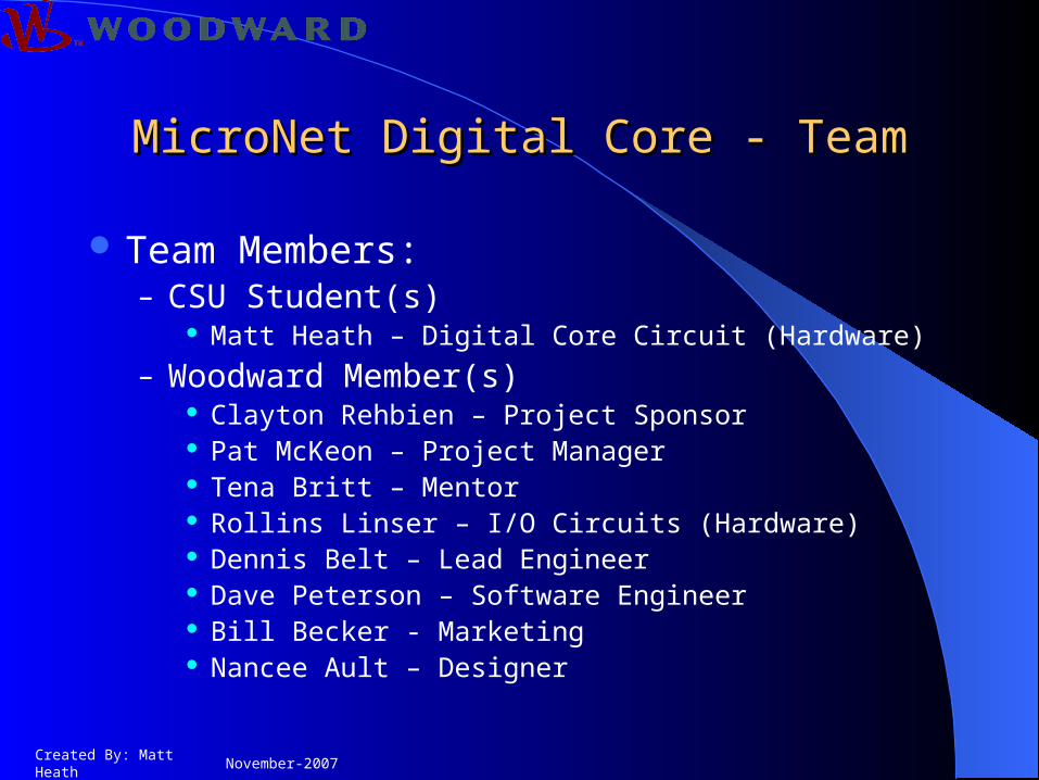
MicroNet Digital Core - TeamMicroNet Digital Core - Team
Team Members:– CSU Student(s)
Matt Heath – Digital Core Circuit (Hardware)
– Woodward Member(s) Clayton Rehbien – Project Sponsor Pat McKeon – Project Manager Tena Britt – Mentor Rollins Linser – I/O Circuits (Hardware) Dennis Belt – Lead Engineer Dave Peterson – Software Engineer Bill Becker - Marketing Nancee Ault – Designer
November-2007Created By: Matt Heath
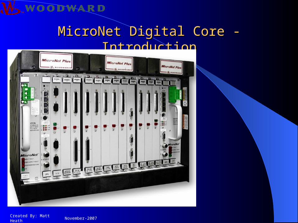
MicroNet Digital Core - IntroductionMicroNet Digital Core - Introduction
November-2007Created By: Matt Heath
MicroNet Digital Core – OverviewMicroNet Digital Core – Overview
Reason for the Project– Current modules are facing parts obsolescence.
Intel 196 Family Motorola DSP5600 Family
– Discrete I/O
Circuit Design– Circuit and Layout re-use for all modules– Reduce circuit real estate on current modules
November-2007Created By: Matt Heath
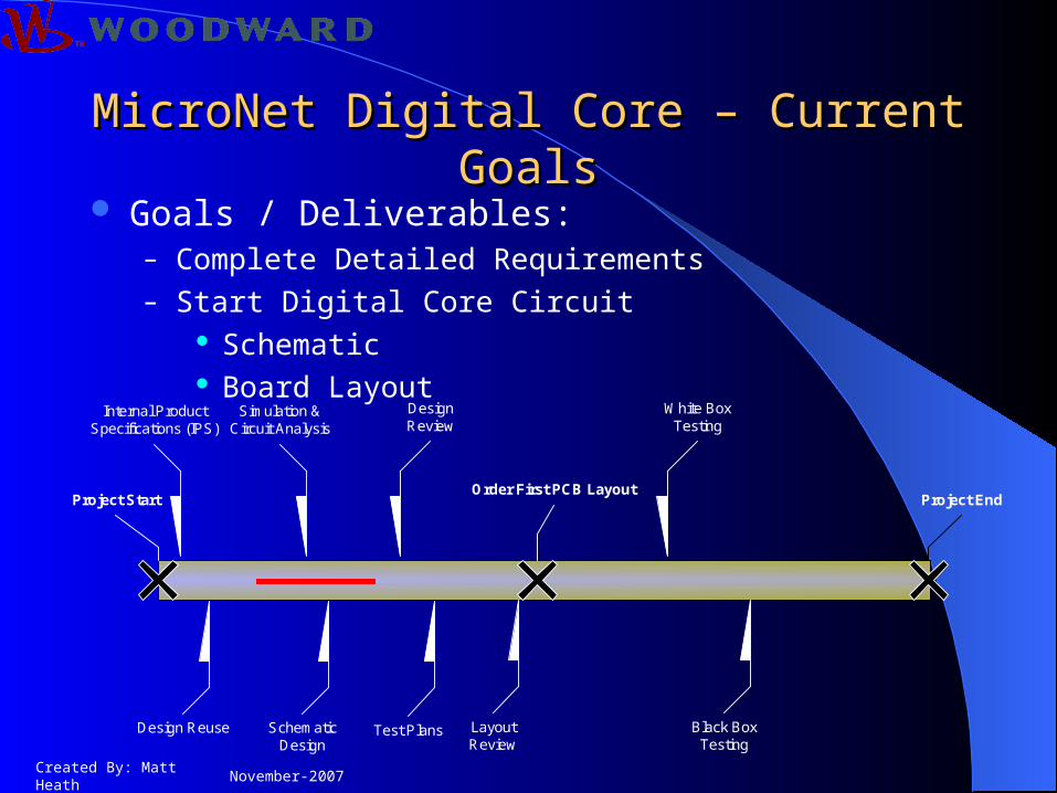
MicroNet Digital Core – Current GoalsMicroNet Digital Core – Current Goals Goals / Deliverables:
– Complete Detailed Requirements– Start Digital Core Circuit
Schematic Board Layout
Internal ProductSpecifications (IPS)
Design Reuse
Simulation &Circuit Analysis
SchematicDesign
Project StartOrder First PCB Layout
DesignReview
LayoutReview
White BoxTesting
Test Plans
Project End
Black BoxTesting
November-2007Created By: Matt Heath
Core 565-CPU
Fro
nt P
anel
Mic
roN
et V
ME
bus
P1
Mic
roN
et V
ME
bus
P2
BUSINTERFACE
? MByte SRAM
512kB MRAM On-Board NV RAM
Boot Sectors
RUNFAULT
GR
RD
LED DRIVERRUNFAULT
VME HotSwap
FPGAVMEBUS
CONTROLLER(Slave)
CAB(15:0)
DATABUFFERS
VMEADDRESS
XCVRVA(23:1)
CTRLXCVR
VD(15:0)
VC(11:0)
VMEDATAXCVR
VDB(15:0)
VAB(11:0)
DPRAM
1.2V 2.5V 3.3VIsol 5V
coms, CAN
2.5V 3.3V
Power Supply
LOCAL PWRMONITOR
5.0V_FAIL3.3V_FAIL2.6V FAIL2.5V_FAIL1.2V_FAIL
RESET*
VME_24
Isolated 5V PowerSupply
32MHz
VME_5V
1.2V
LOCAL POWERSUPPLY
2.6V
2.5v
3.3V
3.3V
HotSwap Ctrl(+5V to 3.3V)
3.3V
2.5V
_cs6_vme, _lp_oerwb_cfg3,
_lp_tack, _lp_terr_cpu_req
4 MHz
ADDRESSBUFFERS
CDB(15:0)
QSMCM A
I2C32.768 KHz
MCP565
JTAG
SRAM2 X 256
JTAG
VD(31:16)VME
DATAXCVR
VD
B(3
1:1
6)
ModuleHealth
Monitor
2.6V
5.0V
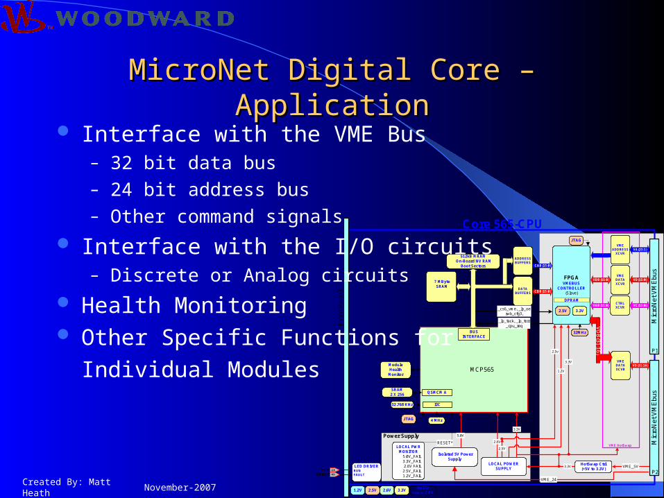
MicroNet Digital Core – ApplicationMicroNet Digital Core – Application Interface with the VME Bus
– 32 bit data bus– 24 bit address bus– Other command signals
Interface with the I/O circuits– Discrete or Analog circuits
Health Monitoring Other Specific Functions for
Individual Modules
November-2007Created By: Matt Heath
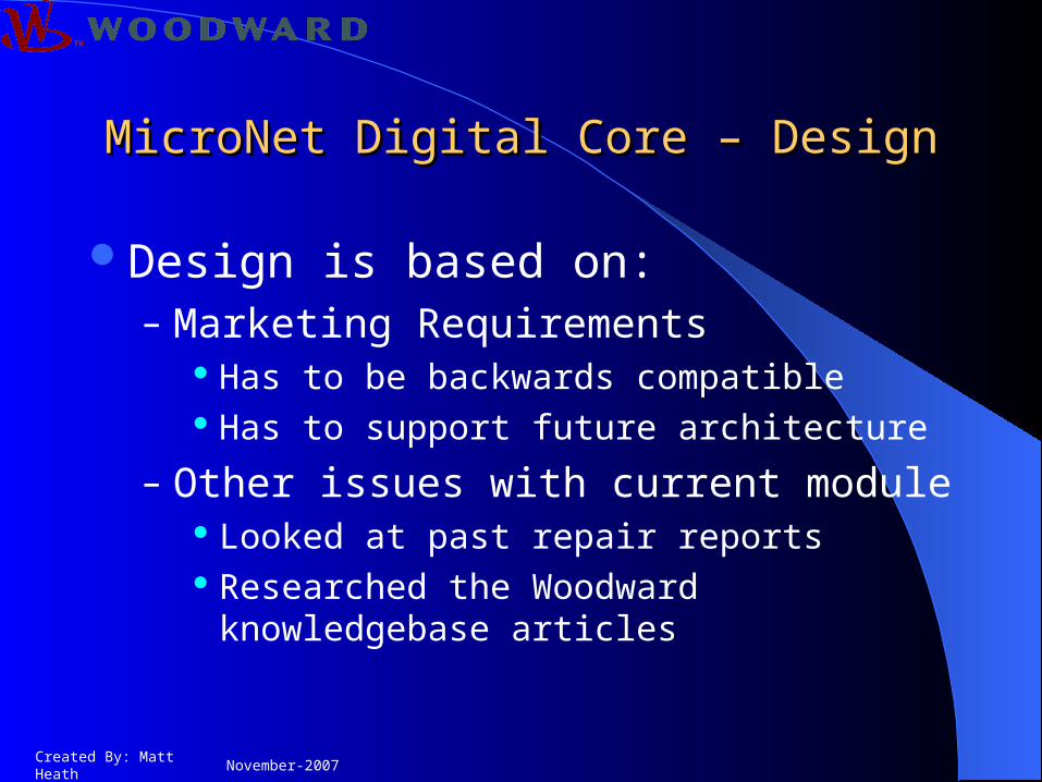
MicroNet Digital Core – DesignMicroNet Digital Core – Design
Design is based on:– Marketing Requirements
Has to be backwards compatible Has to support future architecture
– Other issues with current module Looked at past repair reports Researched the Woodward knowledgebase articles
November-2007Created By: Matt Heath
MicroNet Digital Core – DesignMicroNet Digital Core – Design
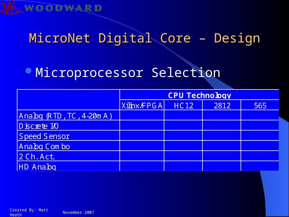
Microprocessor Selection
Xilinx/FPGA HC12 2812 565Analog (RTD, TC, 4-20mA)Discrete I/OSpeed SensorAnalog Combo2 Ch. Act.HD Analog
CPU Technology
November-2007Created By: Matt Heath
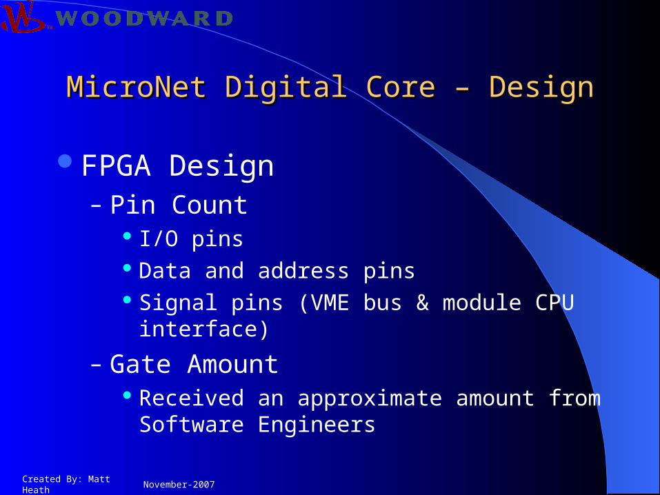
MicroNet Digital Core – DesignMicroNet Digital Core – Design
FPGA Design– Pin Count
I/O pins Data and address pins Signal pins (VME bus & module CPU interface)
– Gate Amount Received an approximate amount from Software
Engineers
November-2007Created By: Matt Heath
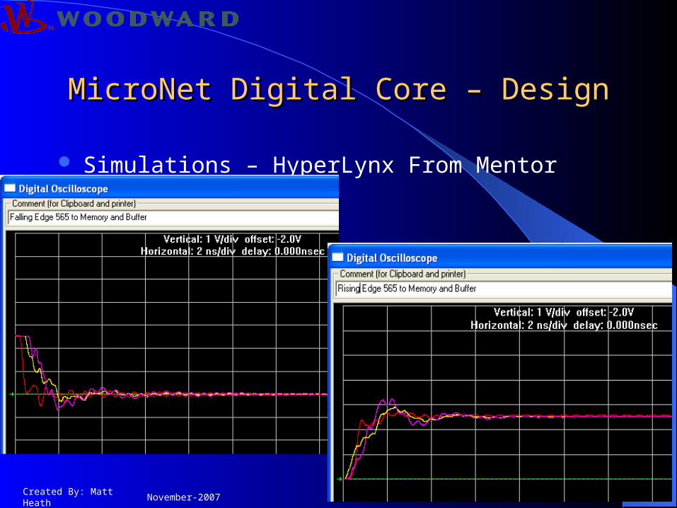
MicroNet Digital Core – DesignMicroNet Digital Core – Design
Simulations – HyperLynx From Mentor Graphics
November-2007Created By: Matt Heath
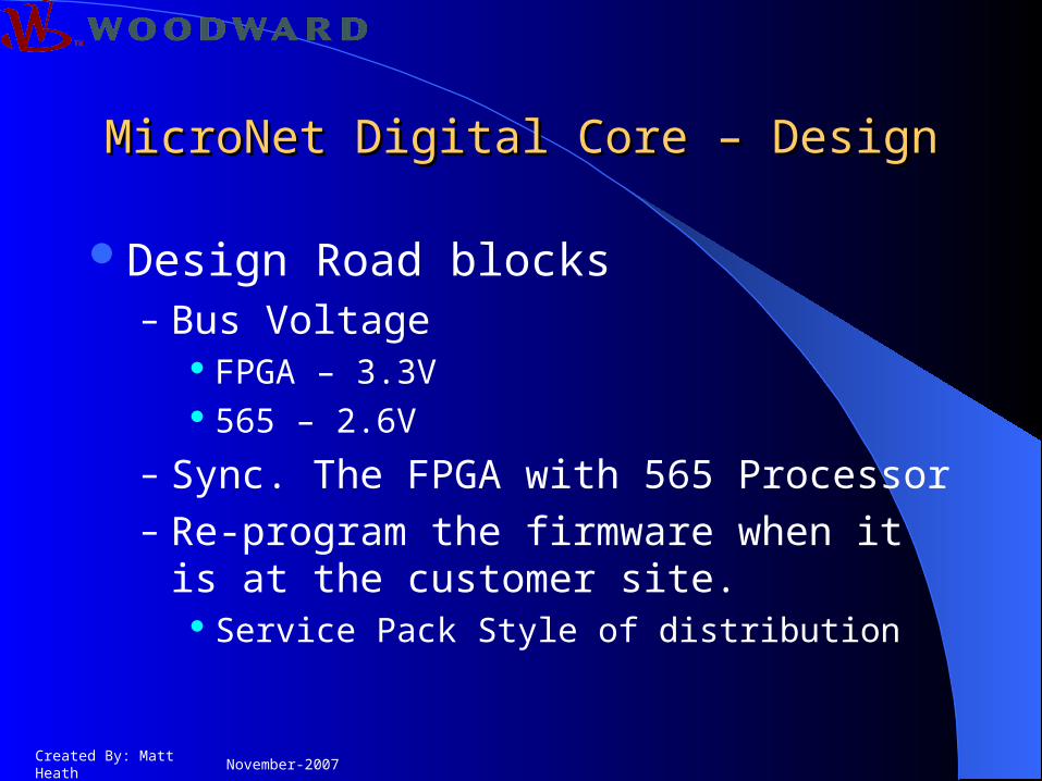
MicroNet Digital Core – DesignMicroNet Digital Core – Design
Design Road blocks– Bus Voltage
FPGA – 3.3V 565 – 2.6V
– Sync. The FPGA with 565 Processor– Re-program the firmware when it is at the
customer site. Service Pack Style of distribution
November-2007Created By: Matt Heath
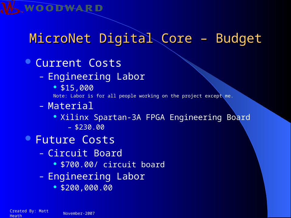
MicroNet Digital Core – BudgetMicroNet Digital Core – Budget
Current Costs– Engineering Labor
$15,000Note: Labor is for all people working on the project except me.
– Material Xilinx Spartan-3A FPGA Engineering Board
– $230.00
Future Costs– Circuit Board
$700.00/ circuit board
– Engineering Labor $200,000.00
November-2007Created By: Matt Heath
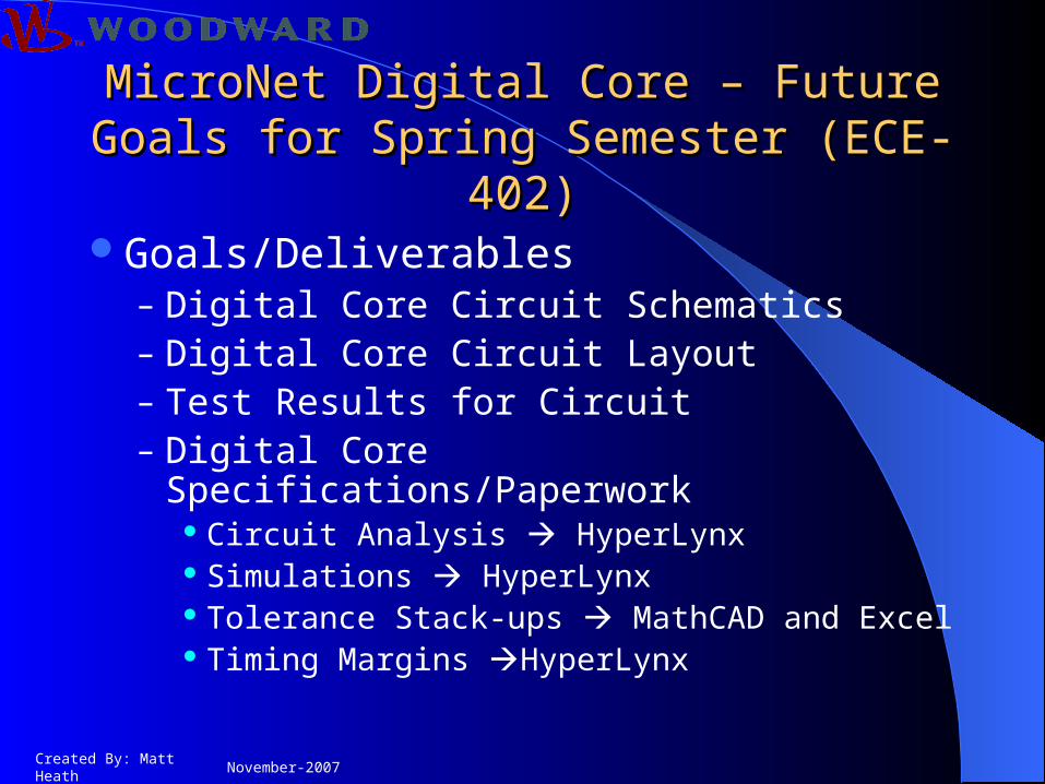
MicroNet Digital Core – Future Goals for MicroNet Digital Core – Future Goals for Spring Semester (ECE-402)Spring Semester (ECE-402)
Goals/Deliverables– Digital Core Circuit Schematics– Digital Core Circuit Layout– Test Results for Circuit– Digital Core Specifications/Paperwork
Circuit Analysis HyperLynx Simulations HyperLynx Tolerance Stack-ups MathCAD and Excel Timing Margins HyperLynx
November-2007Created By: Matt Heath
MicroNet Digital Core – ConclusionMicroNet Digital Core – Conclusion
Thank You!


![DAN Deplakfactor...CHIP HEATH & DAN HEATH De plakfactor Waarom sommige ideeën aanslaan en andere niet De plakfactor CHIP HEATH & DAN HEATH [Made to Stick] Waarom zijn broodjeaapverhalen](https://static.fdocument.pub/doc/165x107/5f96feee962b722a832f99d4/dan-deplakfactor-chip-heath-dan-heath-de-plakfactor-waarom-sommige-ideen.jpg)