NN32251A INTEGRATED WIRELESS POWER SUPPLY · PDF fileASK demodulation for both current and ......
31
Page 1 of 30 NN32251A Product Standards Integrated wireless power transmitter controller WPC Ver. 1.1 ready MCU embedded Half-bridge gate driver : 4ch (full-bridge gate driver : 2ch also configurable) Single-coil (Type A11) supported Expanded free positioning using multi-coils up to 4 coils (Type A6) Highly accurate voltage and current monitor for inverters Output controlled by frequency or duty, defined in Qi. ASK demodulation for both current and voltage signals (Qi compliant) Input voltage range : VADP, VINV : 4.6 to 19.5V Supports Under Voltage Lockout , Thermal Shutdown, Over Current Detection Short-circuit protection at inverter output Temperature Detecting Circuit : 3ch LED indicator : 2ch package : 64 pins HQFP (size : 12mm 12mm) INTEGRATED WIRELESS POWER SUPPLY TRANSMITTER, Qi (WIRELESS POWER CONSORTIUM) COMPLIANT NN32251A is a wireless power system controller IC which is compliant with Qi version 1.1 of the System Description Wireless Power Transfer, Volume 1 for Low Power, defined by Wireless Power Consortium. NN32251A is a controller IC of a power transmitter (Tx) which can supply power to any Qi-compliant wireless chargers. Power transmission of over 5W is also available with the combination of AN32258A used for a receiver (Rx) . ・WPC-compliant wireless charger http://www.semicon.panasonic.co.jp/en/ FEATURES DESCRIPTION APPLICATIONS Wireless Power System Cp TX Coil Wireless Power Communication Tx Inverter VIN Transmitter (Tx) NN32251A Cd AN32258A IOUT Control Cs IC RX Coil Rectifier VRECT Charger + OUT Receiver (Rx) Co Doc No. TA4-EA-062!4 Revision. ! Established : 2014-01-27 Revised : 2014-0!-10
Transcript of NN32251A INTEGRATED WIRELESS POWER SUPPLY · PDF fileASK demodulation for both current and ......
Page 1 of 30
NN32251A
Product Standards
Integrated wireless power transmitter controller WPC Ver. 1.1 ready MCU embedded Half-bridge gate driver : 4ch
(full-bridge gate driver : 2ch also configurable) Single-coil (Type A11) supported Expanded free positioning using multi-coils up to 4 coils
(Type A6) Highly accurate voltage and current monitor for inverters Output controlled by frequency or duty, defined in Qi.ASK demodulation for both current and voltage signals
(Qi compliant) Input voltage range : VADP, VINV : 4.6 to 19.5V Supports Under Voltage Lockout , Thermal Shutdown,
Over Current Detection Short-circuit protection at inverter output Temperature Detecting Circuit : 3ch LED indicator : 2ch package : 64 pins HQFP
(size : 12mm 12mm)
INTEGRATED WIRELESS POWER SUPPLY TRANSMITTER,
Qi (WIRELESS POWER CONSORTIUM) COMPLIANT
NN32251A is a wireless power system controller IC which is compliant with Qi version 1.1 of the System Description Wireless Power Transfer, Volume 1 for Low Power, defined by Wireless Power Consortium.
NN32251A is a controller IC of a power transmitter (Tx) which can supply power to any Qi-compliant wireless chargers. Power transmission of over 5W is also available with the combination of AN32258A used for a receiver (Rx) .
・WPC-compliant wireless charger
http://www.semicon.panasonic.co.jp/en/
FEATURES DESCRIPTION
APPLICATIONS
Wireless Power System
Cp
TXCoil
Wireless Power
Communication
Tx
Inve
rter
VIN
Transmitter (Tx)
NN32251ACd
AN32258A
IOUT
Control
Cs
ICRX
Coil
Rec
tifie
r
VRECT Charger
+
OUT
Receiver (Rx)
Co
Doc No. TA4-EA-06234Revision. 3
Established : 2014-01-27Revised : 2014-03-10

Page 2 of 30
NN32251A
Product Standards
DELIVERY INFORMATION
Order Number Package Output Supply Minimum Quantity
NN32251A-VT 64 pin HQFP (12×12 mm) Tray 500pcs
ABSOLUTE MAXIMUM RATINGS
Parameter Symbol Rating Unit Notes
Supply voltageVVADP 21 V
*1VVINV 21 V
Output current IVADP — A *1
Operating ambient temperature Topr – 30 to + 85 C *2
Operating junction temperature Tj -40 to +125 C *2
Storage temperature Tstg – 55 to + 125 C *2
Input voltage range
VSCDET1, VSCDET2, VSCDET3,VSCDET4, VCFB1, VCFB2, VVFB
– 0.3 to 21 V *1
VTEST3, VSELLED1, VTYP1, VSELLED2, VNCO1, VNCO2, VPWR, VSELFOD1,
VSELFOD2,
VTEST4, VFWMD, VTH1, VTH2, VTH3,
– 0.3 to 7 V *1
VTEST2, VENB, VVMODIN, VCMODIN, VCSIN1, VCSIN2, VTEST, VSMBC,
VSMBD,– 0.3 to 4.6 V *1
ESDHBM (Human Body Model) 2 kV —
CDM (Charged Device Model) 1 kV —
Note) This product may sustain permanent damage if the actual condition is higher than the absolute maximum rating stated above. This rating is the maximum stress, and device will not be guaranteed to operate in case it is higher than our stated range. When exposed to the absolute maximum rating for a long time, the reliability of the product may be affected.No voltage or current input is allowed for the pins not listed above. All voltage ratings are relative to the ground level, which is referred to as GNDMC, GNDMOD, GNDA1, GNDA3, GNDP1, and GNDP2.*1:The values are under the condition not exceeding the above absolute maximum ratings and the power dissipation.
*2:Except for the power dissipation, operating ambient temperature, and storage temperature, all ratings are for Ta = 25 C.
Doc No. TA4-EA-06234Revision. 3
Established : 2014-01-27Revised : 2014-03-10

Page 3 of 30
NN32251A
Product Standards
PACKAGE j-a j-CPD
(Ta = 25 C)PD
(Ta = 85 C)Notes
HQFP64 25.5 C / W 1.05 C /W 4.90 W 2.55 W *1
Parameter Pin Name Min. Typ. Max. Unit Notes
Supply voltage range VVADP, VVINV 4.6 12 19.5 V *2
POWER DISSIPATION RATING
Note). For the actual usage, please refer to the PD-Ta characteristics diagram in the package specification, and follow the power supply voltage, load and ambient temperature conditions to ensure that there is enough margin and the thermal design does not exceed the allowable value.
*1 : glass epoxy board (4 layers) [50 50 0.8 t (mm)]
CAUTIONAlthough this device has limited built-in ESD protection circuit, permanent damage may occur on it.Therefore, proper ESD precautions are recommended to avoid electrostatic damage to the MOS gates
RECOMMENDED OPERATING CONDITIONS
Note) *2 :The values are under the condition not exceeding the above absolute maximum ratings and the power dissipation.
Doc No. TA4-EA-06234Revision. 3
Established : 2014-01-27Revised : 2014-03-10
Page 4 of 30
NN32251A
Product Standards
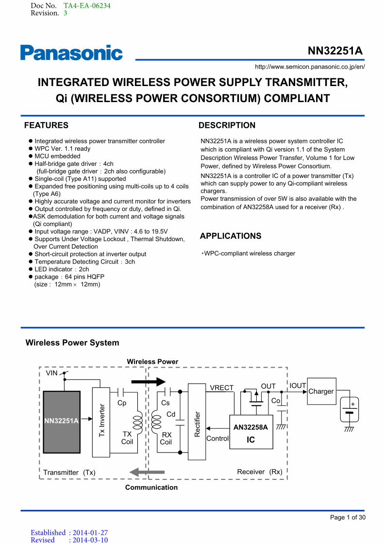
ELECRTRICAL CHARACTERISTICSVVADP = 12 V, VVINV = 12 V, Ta = 25 C 2 C unless otherwise noted.
Parameter Symbol Condition Limits
Unit NoteMin Typ Max
Current Consumption
Quiescent current ISTBY ENB=L 6.48 8.10 9.72 mA
Operating current IOPR ENB=H 18.0 22.6 27.0 mA
Half-Bridge Gate Driver
Minimum switching frequency FSWMIN 108 110 112 kHz
Maximum switching frequency FSWMAX 200 205 210 kHz
Accuracy of switching frequency FSWCA — — 0.4 kHz
Minimum duty DRMIN — — 10 %
Maximum duty DRMAX 50 — — %
High-side Output – H level VHSH Isource=1mAVVINV
-0.3— — V
High-side Output – L level VHSL Isink=1mA — —VVINV
-4.7V
Low-side Output – H level VLSH Isource=1mA 3.8 — — V
Low-side Output – L level VLSL Isink=1mA — — 0.2 V
LDO4.1V
Output voltage VOUT41 Iout=20mA 4.0 4.1 4.2 V
LDO3.3V (for internal circuit)
Output voltage VOUT33 Iout=1mA 3.2 3.3 3.4 V
LDO1.8V (for internal circuit)
Output voltage VOUT18 Iout=1mA 1.7 1.8 1.9 V
Doc No. TA4-EA-06234Revision. 3
Established : 2014-01-27Revised : 2014-03-10
Page 5 of 30
NN32251A
Product Standards
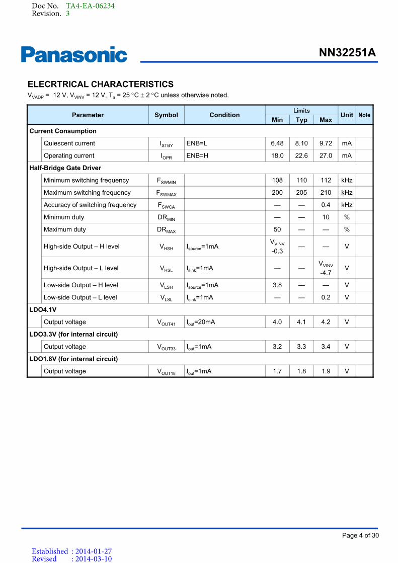
ELECRTRICAL CHARACTERISTICS (Continued)VVADP = 12 V, VVINV = 12 V, Ta = 25 C 2 C unless otherwise noted.
Parameter Symbol Condition Limits
Unit NoteMin Typ Max
Under-Voltage Lock-Out (UVLO)
Under-voltage lock-out VUVLOR 3.85 4.00 4.15 V
Hysteresis on UVLO VUVLOHYSHysteresis of UVLO
detection and release0.70 0.75 0.80 V
LED Driver
Saturation voltage VLEDSAT Iout=10mA — — 0.3 V
ENB Input Voltage
“H” input threshold VIHENB 2.6 — — V
“L” input threshold VILENB — — 0.6 V
TYP1, SELLED2, NCO1, NCO2, PWR, SELFOD1, SELFOD2, SELLED1 Input Voltage
“H” input threshold VIHTYP1 3.3 — — V
“L” input threshold VILTYP1 — — 0.8 V
Doc No. TA4-EA-06234Revision. 3
Established : 2014-01-27Revised : 2014-03-10

Page 6 of 30
NN32251A
Product Standards
Parameter Symbol Condition Limits
Unit NoteMin Typ Max
ASK demodulation
Current demodulation input threshold
ITHMOD — 5 — mA *1
Voltage demodulation input threshold
VTHMOD — 50 — mV *1
Inverter Short-Circuit Protection (SCP)
Detection time VOCPR Time till oscillation stops — 100 — us
Thermal Shutdown (TSD)
Detection threshold TSDR65 C, with the
recommended parts— 0.648 — V *1
Release threshold TSDF65 C, with the
recommended parts— 0.727 — V *1
Over-Current Protection (OCP)
Detected Current 1-1 IOCp11
Type A11, R4=25mohm
VADP=5V, VVINV=5V
Before power transfer *2
— 0.8 — A *1
Detected Current 1-2 IOCp12
Type A11, R4=25mohm
VADP=5V, VVINV=5V
At power transfer *3
— 3.0 — A *1
Detected Current 2-1 IOCp21
Type A6, R4=50mohm
Before power transfer *2— 0.4 — A *1
Detected Current 2-2 IOCp22
Type A6, R4=50mohm
At power transfer *3— 1.5 — A *1
Detected Current 3-1 IOCp31
Type A6, High power
PWR pin (No.9): LDO41V
R4=50mohm
Before power transfer *2
— 0.4 — A *1
Detected Current 3-2 IOCp32
Type A6, High power
PWR pin (No.9): LDO41V
R4=50mohm
At power transfer *3
— 1.9 — A *1
Note)
*1 : Designed typical values
*2: Conditions at Selection, Ping, and ID & Configuration phases. Refer to Power Transfer Phases section for more details.
*3: Conditions at Power Transfer phase. Refer to Power Transfer Phases section for more details.
ELECRTRICAL CHARACTERISTICS (Continued)VVADP = 12 V, VVINV = 12 V, Ta = 25 C 2 C unless otherwise noted.
Doc No. TA4-EA-06234Revision. 3
Established : 2014-01-27Revised : 2014-03-10
Page 7 of 30
NN32251A
Product Standards
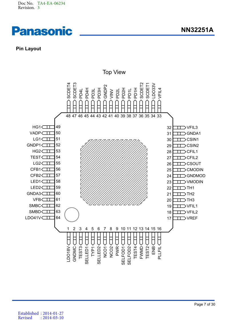
Top View
1 2 3 4 5 6 7 8 9 10 11 12 13 14 15 16
17
18
19
20
21
22
23
24
25
26
27
28
29
30
31
32
33343536373839404142434445464748
49
50
51
52
53
54
55
56
57
58
59
60
61
62
63
64 VREF
VFIL2
VFIL1
TH3
TH2
TH1
VMODIN
GNDMOD
CMODIN
CSOUT
CFIL2
CFIL1
CSIN2
CSIN1
GNDA1
VFIL3HG1
VADP
LG1
GNDP1
HG2
TEST
LG2
CFB1
CFB2
LED1
LED2
GNDA3
VFB
SMBC
SMBD
LDO41V
LDO
18V
GN
DM
C
TE
ST
3
SE
LLE
D1
TY
P1
SE
LLE
D2
NC
O1
NC
O2
PW
R
SE
LFO
D1
SE
LFO
D2
TE
ST
4
FW
MD
TE
ST
2
EN
B
PLL
FIL
SC
DE
T4
SC
DE
T3
PD
4L
PD
4H
PD
3L
PD
3H
GN
DP
2
VIN
V
PD
2L
PD
2H
PD
1L
PD
1H
SC
DE
T2
SC
DE
T1
LDO
33V
VF
IL4
Pin Layout
Doc No. TA4-EA-06234Revision. 3
Established : 2014-01-27Revised : 2014-03-10
Page 8 of 30
NN32251A
Product Standards
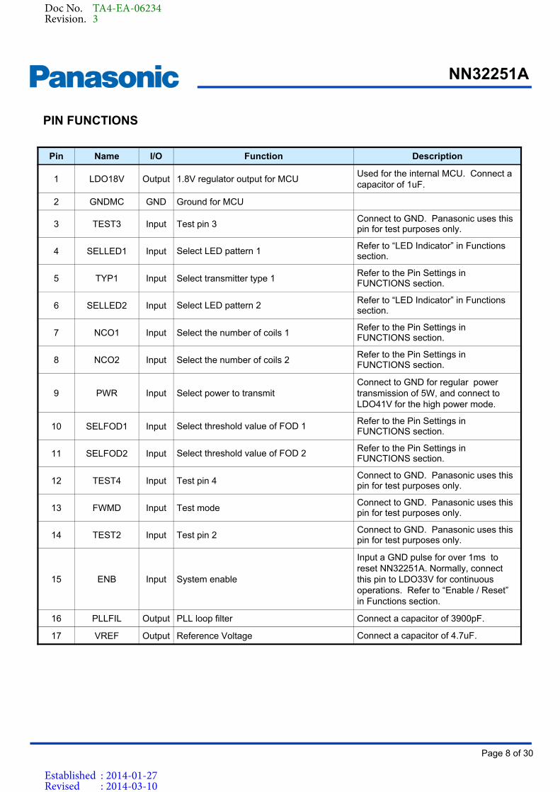
Pin Name I/O Function Description
1 LDO18V Output 1.8V regulator output for MCUUsed for the internal MCU. Connect a capacitor of 1uF.
2 GNDMC GND Ground for MCU
3 TEST3 Input Test pin 3Connect to GND. Panasonic uses this pin for test purposes only.
4 SELLED1 Input Select LED pattern 1Refer to “LED Indicator” in Functions section.
5 TYP1 Input Select transmitter type 1Refer to the Pin Settings in FUNCTIONS section.
6 SELLED2 Input Select LED pattern 2Refer to “LED Indicator” in Functions section.
7 NCO1 Input Select the number of coils 1Refer to the Pin Settings in FUNCTIONS section.
8 NCO2 Input Select the number of coils 2Refer to the Pin Settings in FUNCTIONS section.
9 PWR Input Select power to transmitConnect to GND for regular power transmission of 5W, and connect to LDO41V for the high power mode.
10 SELFOD1 Input Select threshold value of FOD 1Refer to the Pin Settings in FUNCTIONS section.
11 SELFOD2 Input Select threshold value of FOD 2Refer to the Pin Settings in FUNCTIONS section.
12 TEST4 Input Test pin 4Connect to GND. Panasonic uses this pin for test purposes only.
13 FWMD Input Test modeConnect to GND. Panasonic uses this pin for test purposes only.
14 TEST2 Input Test pin 2Connect to GND. Panasonic uses this pin for test purposes only.
15 ENB Input System enable
Input a GND pulse for over 1ms to reset NN32251A. Normally, connect this pin to LDO33V for continuous operations. Refer to “Enable / Reset” in Functions section.
16 PLLFIL Output PLL loop filter Connect a capacitor of 3900pF.
17 VREF Output Reference Voltage Connect a capacitor of 4.7uF.
PIN FUNCTIONS
Doc No. TA4-EA-06234Revision. 3
Established : 2014-01-27Revised : 2014-03-10

Page 9 of 30
NN32251A
Product Standards
Pin Name I/O Function Description
18 VFIL2 Output Voltage detection active filter 2 Connect a capacitor of 1000pF.
19 VFIL1 Output Voltage detection active filter 1 Connect a capacitor 2200pF.
20 TH3 Input Thermistor voltage 3
Connect a thermistor, and place it where temperature is measured. Connect to LDO33V if a thermistor is not connected.
21 TH2 Input Thermistor voltage 2
Connect a thermistor, and place it where temperature is measured. Connect to LDO33V if a thermistor is not connected.
22 TH1 Input Thermistor voltage 1
Connect a thermistor, and place it where temperature is measured. Connect to LDO33V if a thermistor is not connected.
23 VMODIN Input ASK voltage demodulation Input ASK voltage from Rx.
24 GNDMOD GND GND for demodulator
25 CMODIN Input ASK current demodulation Input ASK current from Rx
26 CSOUT Output Current sensor output for inverterConnect a capacitor of 68000pF between CMODIN and this pin.
27 CFIL2 Output Current detection active filter 2 Connect a capacitor of 1000pF.
28 CFIL1 Output Current detection active filter 1 Connect a capacitor of 3300pF.
29 CSIN2 Input Current detection for inverter 2 Connect a resistor of 25m ohm or 50m ohm, between CSIN1 and CSIN2.30 CSIN1 Input Current detection for inverter 1
31 GNDA1 GND GND for analog circuit 1
32 VFIL3 Output Voltage detection active filter 3 Connect a capacitor of 3300pF.
33 VFIL4 Output Voltage detection active filter 4 Connect a capacitor of 1000pF.
34 LDO33V Output 3.3V regulator output Connect a capacitor of 1uF.
35 SCDET1 Input Inverter short-circuit detection 1Connect to the drain of first inverter driven from PD1H and PD1L pins.
36 SCDET2 Input Inverter short-circuit detection 2Connect to the drain of second inverter driven from PD2H and PD2L pins.
37 PD1H Output High-side gate driver of inverter 1Connect to the gate of first inverter PMOS
38 PD1L Output Low-side gate driver of inverter 1Connect to the gate of first inverter NMOS
39 PD2H Output High-side gate driver of inverter 2Connect to the gate of second inverter PMOS
40 PD2L Output Low-side gate driver of inverter 2Connect to the gate of second inverter NMOS
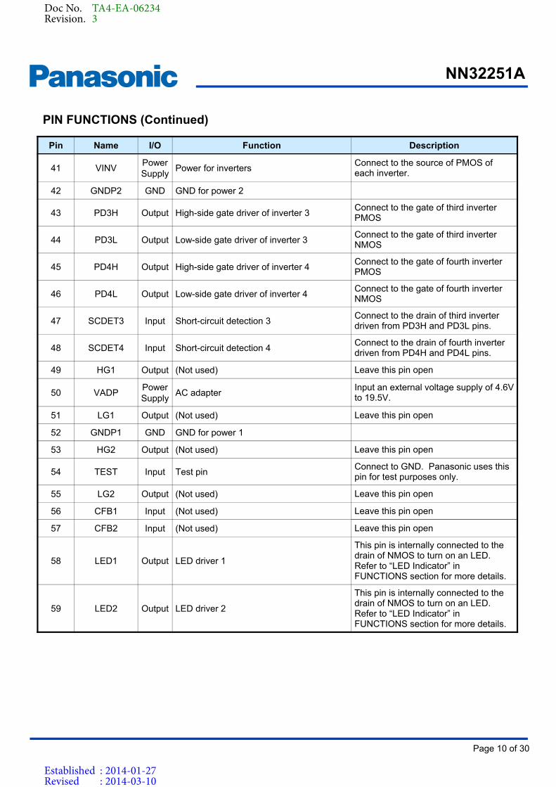
PIN FUNCTIONS (Continued)
Doc No. TA4-EA-06234Revision. 3
Established : 2014-01-27Revised : 2014-03-10
Page 10 of 30
NN32251A
Product Standards
Pin Name I/O Function Description
41 VINVPower Supply
Power for invertersConnect to the source of PMOS of each inverter.
42 GNDP2 GND GND for power 2
43 PD3H Output High-side gate driver of inverter 3Connect to the gate of third inverter PMOS
44 PD3L Output Low-side gate driver of inverter 3Connect to the gate of third inverter NMOS
45 PD4H Output High-side gate driver of inverter 4Connect to the gate of fourth inverter PMOS
46 PD4L Output Low-side gate driver of inverter 4Connect to the gate of fourth inverter NMOS
47 SCDET3 Input Short-circuit detection 3Connect to the drain of third inverter driven from PD3H and PD3L pins.
48 SCDET4 Input Short-circuit detection 4Connect to the drain of fourth inverter driven from PD4H and PD4L pins.
49 HG1 Output (Not used) Leave this pin open
50 VADPPower Supply
AC adapterInput an external voltage supply of 4.6V to 19.5V.
51 LG1 Output (Not used) Leave this pin open
52 GNDP1 GND GND for power 1
53 HG2 Output (Not used) Leave this pin open
54 TEST Input Test pin Connect to GND. Panasonic uses this pin for test purposes only.
55 LG2 Output (Not used) Leave this pin open
56 CFB1 Input (Not used) Leave this pin open
57 CFB2 Input (Not used) Leave this pin open
58 LED1 Output LED driver 1
This pin is internally connected to the drain of NMOS to turn on an LED.Refer to “LED Indicator” in FUNCTIONS section for more details.
59 LED2 Output LED driver 2
This pin is internally connected to the drain of NMOS to turn on an LED.Refer to “LED Indicator” in FUNCTIONS section for more details.
PIN FUNCTIONS (Continued)
Doc No. TA4-EA-06234Revision. 3
Established : 2014-01-27Revised : 2014-03-10

Page 11 of 30
NN32251A
Product Standards
Pin Name I/O Function Description
60 GNDA3 GND GND for analog circuit 3
61 VFB Input (Not used) Leave this pin open
62 SMBCInput/Output
Clock for test modeConnect to GND. Panasonic uses this pin for test purposes only.
63 SMBDInput/Output
Data for test modeConnect to GND. Panasonic uses this pin for test purposes only.
64 LDO41V Output 4.1V regulator outputConnect a capacitor of 1uF. LED’s can be connected to this pin.
PIN FUNCTIONS (Continued)
Doc No. TA4-EA-06234Revision. 3
Established : 2014-01-27Revised : 2014-03-10

Page 12 of 30
NN32251A
Product Standards
CIRCUIT DIAGRAM
(Tx Type:A11 Single coil)
Cur
rent
Sen
se
Res
isto
r
Pow
er S
uppl
y (5
.0V
)
EN
B C
on
tro
l3.
3V:a
ctiv
e0V
:res
et
LDO
33V
D3L2
A11 (0
.1u
F*4
)
Q5
Q7
R2 1k
C190.01uF
R3 10k
R425m
C3
3300
pF
C4
1000
pF
C5
6800
0pF
C202200pF
Opt
iona
l T
herm
isto
r
LDO
41V
R9
560
R10
560
D2
D1
R12
R7 R14 R15
C8
1uF
C71000pF
C62200pF
C24
10u
FC
4210
uF
Dut
y C
ontr
olle
r10
%-5
0%
PLL
105k
Hz-
205k
Hz
0.4k
Hz
step
Dut
yC
ontr
olF
requ
ency
Con
trol
12bi
ts A
DC
Reg
iste
rC
hann
el S
elec
tion
Dea
d T
ime
Con
trol
VADP
LED1
LED2
VREFT
YP
1 GN
DM
C
SM
BD
Ser
ial
I/F
TE
ST
3
TH1
TH2
TH3
LDO41V
CSIN1
CSIN2
VMODIN
VFIL1
VFIL2
LDO18V
CFIL1
CFIL2
PD
1H
PD
1L
PD
2H
PD
2L
PD
3L
PD
3H
PD
4L
PD
4H
GNDA1
GNDP1
GNDP2
TEST
GN
DA
3
LDO33V
Inve
rter
Cur
rent
Mea
sure
Inve
rter
Vol
tage
Mea
sure
GNDMODS
MB
C
SE
LLE
D2
NC
O1
NC
O2
PW
R
SE
LFO
D1
SE
LFO
D2
Reg
ulat
or4.
1V
FW
MD
TE
ST
2
EN
B
VFIL3
VFIL4
Tem
pera
ture
Mea
sure
PLLFIL
CSOUT
CMODIN
TE
ST
4
SC
DE
T1
SC
DE
T2
SC
DE
T3
SC
DE
T4
VIN
V
HG
1
LG1
HG
2
LG2
CFB1
CFB2
VFB
Hal
f-B
ridge
Gat
e D
river
Dea
d T
ime
Con
trol
ler
Leve
l Shi
fter
Cha
nnel
Sel
ecto
r
Sho
rt C
ircui
tP
rote
ctio
n
C18C28C29
C30
Vol
tage
Sig
nal
Dem
odul
ator
Cur
rent
Sig
nal
Dem
odul
ator
Reg
ulat
or1.
8V
3rdor
der
5kH
zLP
F
3rdor
der
5kH
zLP
F
R8
R11 R16 R17
R6
R13 R18 R19
Tem
p.M
onito
r
8bits
Mic
ro-
Con
trol
ler
SE
LLE
D1
C9
1uF
C10
4.7u
F
C11
1uF
Ban
d G
apR
efer
ence
LED
Driv
erR
egul
ator
3.3V
UV
LO
C12
3900
pF
C13
1000
pF
C14
3300
pF
C15
10u
FC
160.
01u
FC
2310
uF
3rdor
der
5kH
zLP
F
Clo
ck
Ser
ial
I/F
Fla
shM
emor
y
60 15 14 13 12 11 10 9 8 7 6 5 4 2 3
20
21
22
1
24
18
19
23
25
26
27
28
29
30
42
31
4846454744433640393538374155535149
64
17
59
58
34
16
33
32
50
54
52
61
57
56
62 63
SM
bus
I/F
LDO
41V
6.3u
H
Q6
Q8
LDO
41V
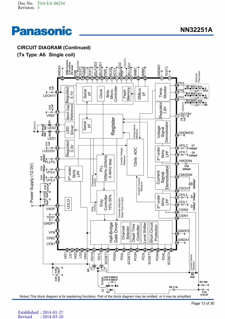
Notes) This block diagram is for explaining functions. Part of the block diagram may be omitted, or it may be simplified.
Doc No. TA4-EA-06234Revision. 3
Established : 2014-01-27Revised : 2014-03-10
Page 13 of 30
NN32251A
Product Standards
CIRCUIT DIAGRAM (Continued)
(Tx Type:A6 Single coil)
Cur
rent
Sen
se
Res
isto
r
Pow
er S
uppl
y (1
2.0V
)
EN
B C
on
tro
l3.
3V:a
ctiv
e0V
:res
et
LDO
33V
D3L2
Q5
R2 3.3k
R3 39k
R450m
C3
3300
pF
C4
1000
pF
C5
6800
0pF
C202200pF
Opt
iona
l T
herm
isto
r
R9
560
R10
560
D2
D1
R12
R7 R14 R15
C8
1uF
C71000pF
C62200pF
C24
10u
FC
4210
uF
Dut
y C
ontr
olle
r10
%-5
0%
PLL
105k
Hz-
205k
Hz
0.4k
Hz
step
Dut
yC
ontr
olF
requ
ency
Con
trol
12bi
ts A
DC
Reg
iste
rC
hann
el S
elec
tion
Dea
d T
ime
Con
trol
VADP
LED1
LED2
VREF
TY
P1 G
ND
MC
SM
BD
Ser
ial
I/F
TE
ST
3
TH1
TH2
TH3
LDO41V
CSIN1
CSIN2
VMODIN
VFIL1
VFIL2
LDO18V
CFIL1
CFIL2
PD
1H
PD
1L
PD
2H
PD
2L
PD
3L
PD
3H
PD
4L
PD
4H
GNDA1
GNDP1
GNDP2
TEST
GN
DA
3
LDO33V
Inve
rter
Cur
rent
Mea
sure
Inve
rter
Vol
tage
Mea
sure
GNDMODS
MB
C
NC
O1
NC
O2
PW
R
Reg
ulat
or4.
1V
FW
MD
TE
ST
2
EN
B
VFIL3
VFIL4
Tem
pera
ture
Mea
sure
PLLFIL
CSOUT
CMODIN
TE
ST
4
SC
DE
T1
SC
DE
T2
SC
DE
T3
SC
DE
T4
VIN
V
HG
1
LG1
HG
2
LG2
CFB1
CFB2
VFB
Hal
f-B
ridge
Gat
e D
river
Dea
d T
ime
Con
trol
ler
Leve
l Shi
fter
Cha
nnel
Sel
ecto
r
Sho
rt C
ircui
tP
rote
ctio
n
C28 0.068uF
Vol
tage
Sig
nal
Dem
odul
ator
Cur
rent
Sig
nal
Dem
odul
ator
Reg
ulat
or1.
8V
3rdor
der
5kH
zLP
F
3rdor
der
5kH
zLP
F
R8
R11 R16 R17
R6
R13 R18 R19
Tem
p.M
onito
r
8bits
Mic
ro-
Con
trol
ler
C9
1uF
C10
4.7u
F
C11
1uF
Ban
d G
apR
efer
ence
LED
Driv
erR
egul
ator
3.3V
UV
LO
C12
3900
pF
C13
1000
pF
C14
3300
pF
C15
10u
FC
160.
01u
FC
2310
uF
3rdor
der
5kH
zLP
F
Clo
ck
Ser
ial
I/F
60 15 14 13 12 11 10 9 8 7 6 5 4 2 3
20
21
22
1
24
18
19
23
25
26
27
28
29
30
42
31
4846454744433640393538374155535149
64
17
59
58
34
16
33
32
50
54
52
61
57
56
62 63
SM
bus
I/F
LDO
41V
C18 0.068uF
C190.01uF
SE
LLE
D2
SE
LFO
D1
SE
LFO
D2
SE
LLE
D1
LDO
41V
LDO
41V
Fla
shM
emor
y
12.5
uH
Notes) This block diagram is for explaining functions. Part of the block diagram may be omitted, or it may be simplified.
Doc No. TA4-EA-06234Revision. 3
Established : 2014-01-27Revised : 2014-03-10

Page 14 of 30
NN32251A
Product Standards
CIRCUIT DIAGRAM (Continued)
(Tx Type:A6 3-coil array)
LDO
41V
Cur
rent
Sen
se
Res
isto
r
Pow
er S
uppl
y (1
2.0V
)
EN
B C
on
tro
l3.
3V:a
ctiv
e0V
:res
et
LDO
33V
D3L2
Q5
Q7
R2 3.3k
R3 39k
R450m
C3
3300
pF
C4
1000
pF
C5
6800
0pF
C202200pF
Opt
iona
l T
herm
isto
r
R9
560
R10
560
D2
D1
R12
R7 R14 R15
C8
1uF
C71000pF
C62200pF
C24
10u
FC
4210
uF
Dut
y C
ontr
olle
r10
%-5
0%
PLL
105k
Hz-
205k
Hz
0.4k
Hz
step
Dut
yC
ontr
olF
requ
ency
Con
trol
12bi
ts A
DC
Reg
iste
rC
hann
el S
elec
tion
Dea
d T
ime
Con
trol
VADP
LED1
LED2
VREFT
YP
1 GN
DM
C
SM
BD
Ser
ial
I/F
TE
ST
3
TH1
TH2
TH3
LDO41V
CSIN1
CSIN2
VMODIN
VFIL1
VFIL2
LDO18V
CFIL1
CFIL2
PD
1H
PD
1L
PD
2H
PD
2L
PD
3L
PD
3H
PD
4L
PD
4H
GNDA1
GNDP1
GNDP2
TEST
GN
DA
3
LDO33V
Inve
rter
Cur
rent
Mea
sure
Inve
rter
Vol
tage
Mea
sure
GNDMODS
MB
C
NC
O1
NC
O2
PW
R
Reg
ulat
or4.
1V
FW
MD
TE
ST
2
EN
B
VFIL3
VFIL4
Tem
pera
ture
Mea
sure
PLLFIL
CSOUT
CMODIN
TE
ST
4
SC
DE
T1
SC
DE
T2
SC
DE
T3
SC
DE
T4
VIN
V
HG
1
LG1
HG
2
LG2
CFB1
CFB2
VFB
Hal
f-B
ridge
Gat
e D
river
Dea
d T
ime
Con
trol
ler
Leve
l Shi
fter
Cha
nnel
Sel
ecto
r
Sho
rt C
ircui
tP
rote
ctio
n
C28 0.068uF
Vol
tage
Sig
nal
Dem
odul
ator
Cur
rent
Sig
nal
Dem
odul
ator
Reg
ulat
or1.
8V
3rdor
der
5kH
zLP
F
3rdor
der
5kH
zLP
F
R8
R11 R16 R17
R6
R13 R18 R19
Tem
p.M
onito
r
8bits
Mic
ro-
Con
trol
ler
C9
1uF
C10
4.7u
F
C11
1uF
Ban
d G
apR
efer
ence
LED
Driv
erR
egul
ator
3.3V
UV
LO
C12
3900
pF
C13
1000
pF
C14
3300
pF
C15
10u
FC
160.
01u
FC
2310
uF
3rdor
der
5kH
zLP
F
Clo
ck
Ser
ial
I/F
60 15 14 13 12 11 10 9 8 7 6 5 4 2 3
20
21
22
1
24
18
19
23
25
26
27
28
29
30
42
31
4846454744433640393538374155535149
64
17
59
58
34
16
33
32
50
54
52
61
57
56
62 63
SM
bus
I/F
LDO
41V
C18 0.068uF
D5L3
C30 0.047uFC25 0.1uF
Q9
C32 0.068uFC26 0.068uF
D7L4
C190.01uF
SE
LLE
D2
SE
LFO
D1
SE
LFO
D2
SE
LLE
D1
LDO
41V
LDO
41V
Fla
shM
emor
y
12.5
uH
12.5
uH
11.5
uH
Notes) This block diagram is for explaining functions. Part of the block diagram may be omitted, or it may be simplified.
Doc No. TA4-EA-06234Revision. 3
Established : 2014-01-27Revised : 2014-03-10

Page 15 of 30
NN32251A
Product Standards
No. Function
1 Power Startup Condition
2 Power Transfer Phases
3 Enable / Reset
4 Power Stop and Resume Controls
5 Pin Settings
6 Transmitter Types
7 LED Indicator
8 Over Current Detection
9 Over Temperature Detection
10 High Power Mode
Functions
NN32251A has the following functions.
1. Power Startup ConditionThe pins VADP (No.50) and VINV (No.41) must be shorted out, because inputting VINV before VADP may result in
breakage of NN32251A.
Follow the rise time of VADP and VINV as defined below.
Symbol
Condition
(not tested at shipment) unit
min typ max
Rise time τrise 50 - - us
VADP [V](shorted to VINV)
t[s]
0.1 X VADP
0.9 X VADP
τrise
Figure A-1. Rise time characteristics of VADP
This condition is based on the circuits described in Evaluation Results followed by this chapter.
Thorough evaluation will be required if the circuit is different.
Doc No. TA4-EA-06234Revision. 3
Established : 2014-01-27Revised : 2014-03-10

Page 16 of 30
NN32251A
Product Standards
2.Power Transfer Phases
NN32251A is compliant with Qi version 1.1 of the System Description Wireless Power Transfer, Volume 1 for Low Power, defined by Wireless Power Consortium.
【At selection phase】
・VADP (Pin 50) : Input 4.6 to 19.5V
・ENB (Pin 15) : Connect LDO33V (Pin 34)
Figure A-2. State machine of power transfer phases
Selection
Ping
ID & Configuration
Power Transfer
Full Charge
Full charge(End Power Transfer Code =0x01)
Full charge(End Power Transfer Code =0x01)
Full charge(End Power Transfer Code =0x01)
・Rx moved・15 minutes passed
Find Rx
Error detected*2
Rx moved
Reconfigure(End Power Transfer Code =0x07)
・Error detected*2
・Try four timesPower transmissionestablished
Error detected*2
・Unexpected packet・Communication error・Timeout
No response
Signal Strength Packet・Unexpected packet・Communication error・Timeout
・Unexpected packet・Communication error・Timeout
Power stoppedApply power signal
Apply power signal
Error
-Tx error detection*2
-Rx error detection(except End Power Transfer Code =0x01、0x07*1) Full-charge detected
(End Power Transfer Code =0x01)
*1: The phase does not change when 0x07 is received at Selection.*2: Errors are detected by over-current protection foreign object detection, and short-circuit protection.
TemperatureError
Power stopped
Over-temperature detected
Over-temperature detected
Over-temperature detected
Over-temperature detected
Temperature decreased(∆5)
Functions (Continued)
Power stoppedApply power signal
Doc No. TA4-EA-06234Revision. 3
Established : 2014-01-27Revised : 2014-03-10

Page 17 of 30
NN32251A
Product Standards
3. Enable / ResetControlling the ENB (Pin 15) can enable, stop, or reset NN32251A. Enable will start NN32251A from the
Select phase. Stop will shut down the entire system on NN32251A. Reset will enable NN32251A after sopping it.
The following figure describes the input requirements.
Power-Stop Condition phase Transition
By Rx
1Full-charge detection
(End Power Transfer Code =0x01)
The phase goes to Full Charge and moves to Selection by either removing the Rx or laying the Rx for over 15 minutes.
2End Power Transfer packet of other conditions than full-charge detection
The phase goes to Error and moves to Selection by
removing the Rx.
By Tx
3Temperature detection
(Over 65)
The phase goes to Temperature Error and moves to
Selection when temperature becomes lower than 60.
4 Over current protection The phase goes to Error and moves to Selection by
removing the Rx.5 Short-circuit protection
4. Power Stop and Resume ControlsNN32251A stops power transmission due to its own protections or control from Rx. The condition to resume
depends on what has stopped the power transmission.
Condition Input to ENB pin
Enable
Stop
Reset
Over 1ms
LDO33V
ENB
34
Regulator33V
NN32251A
15
C111uF
To system control
Figure A-3. External circuit to function ENB pin.
GND
GND
GND
LDO33V
LDO33V
LDO33V
Functions (Continued)
Doc No. TA4-EA-06234Revision. 3
Established : 2014-01-27Revised : 2014-03-10
Page 18 of 30
NN32251A
Product Standards
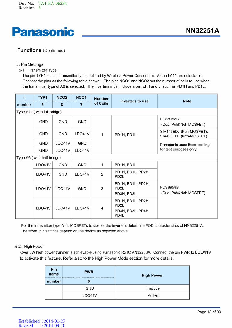
5. Pin Settings5-1. Transmitter Type
The pin TYP1 selects transmitter types defined by Wireless Power Consortium. A6 and A11 are selectable.
Connect the pins as the following table shows. The pins NCO1 and NCO2 set the number of coils to use when
the transmitter type of A6 is selected. The inverters must include a pair of H and L, such as PD1H and PD1L.
For the transmitter type A11, MOSFETs to use for the inverters determine FOD characteristics of NN32251A.
Therefore, pin settings depend on the device as depicted above.
5-2. High Power
Over 5W high power transfer is achievable using Panasonic Rx IC AN32258A. Connect the pin PWR to LDO41V
to activate this feature. Refer also to the High Power Mode section for more details.
Pin name
PWRHigh Power
number 9
GND Inactive
LDO41V Active
Functions (Continued)
f TYP1 NCO2 NCO1 Number of Coils
Inverters to use Notenumber 5 8 7
Type A11 ( with full bridge)
GND GND GND
1 PD1H, PD1L
FDS8958B
(Dual Pch&Nch MOSFET)
GND GND LDO41VSIA445EDJ (Pch-MOSFET), SIA400EDJ (Nch-MOSFET)
GND LDO41V GND Panasonic uses these settings for test purposes onlyGND LDO41V LDO41V
Type A6 ( with half bridge)
LDO41V GND GND 1 PD1H, PD1L
FDS8958B
(Dual Pch&Nch MOSFET)
LDO41V GND LDO41V 2PD1H, PD1L, PD2H, PD2L
LDO41V LDO41V GND 3PD1H, PD1L, PD2H, PD2L
PD3H, PD3L,
LDO41V LDO41V LDO41V 4
PD1H, PD1L, PD2H, PD2L
PD3H, PD3L, PD4H, PD4L
Doc No. TA4-EA-06234Revision. 3
Established : 2014-01-27Revised : 2014-03-10
Page 19 of 30
NN32251A
Product Standards
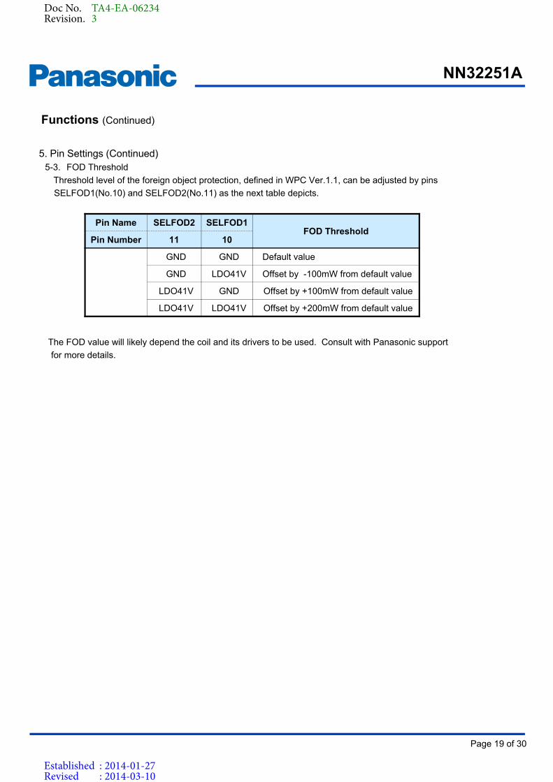
5. Pin Settings (Continued)5-3. FOD Threshold
Threshold level of the foreign object protection, defined in WPC Ver.1.1, can be adjusted by pins
SELFOD1(No.10) and SELFOD2(No.11) as the next table depicts.
Functions (Continued)
Pin Name SELFOD2 SELFOD1FOD Threshold
Pin Number 11 10
GND GND Default value
GND LDO41V Offset by -100mW from default value
LDO41V GND Offset by +100mW from default value
LDO41V LDO41V Offset by +200mW from default value
The FOD value will likely depend the coil and its drivers to be used. Consult with Panasonic support
for more details.
Doc No. TA4-EA-06234Revision. 3
Established : 2014-01-27Revised : 2014-03-10

Page 20 of 30
NN32251A
Product Standards
6.Transmitter Types
NN32251A supports the transmitter types of A6 and A11defined in Qi version 1.1 of the System Description Wireless Power Transfer, Volume 1 for Low Power. The following table shows the detailed specification.
Tx Type A6 A11
Number of coils
One or more Single
Alignment aid free
・A marked Interface Surface
・A visual feedback display
・An audible or haptic feedback
Modulation Method
Frequency or duty Frequency or duty
Operating Frequency
(fop)
Min initial max Min initial max
115kHz 175kHz 205kHz 110kHz 175kHz 205kHz
resolution0.01×fop - 0.7kHz (115…175kHz)
0.015×fop - 1.58kHz (175…205kHz)
0.01×fop - 0.7kHz (115…175kHz)
0.015×fop - 1.58kHz (175…205kHz)
Duty cycle 10% 50% 50% 10% 50% 50%
resolution 0.1% 0.1%
Inverter Voltage
12±5%V 5±5%V
Configuration
Half-bridge Full-bridge
Find more detailed description from WPC homepage.
URL: http://www.wirelesspowerconsortium.com/
A11Coil
NN32251A
Control
A6Coil
VADP/VINV
NN32251A
Control
※NN32251A has 4 inverters to drive up to 4 coils.
VADP/VINV
Functions (Continued)
Doc No. TA4-EA-06234Revision. 3
Established : 2014-01-27Revised : 2014-03-10

Page 21 of 30
NN32251A
Product Standards
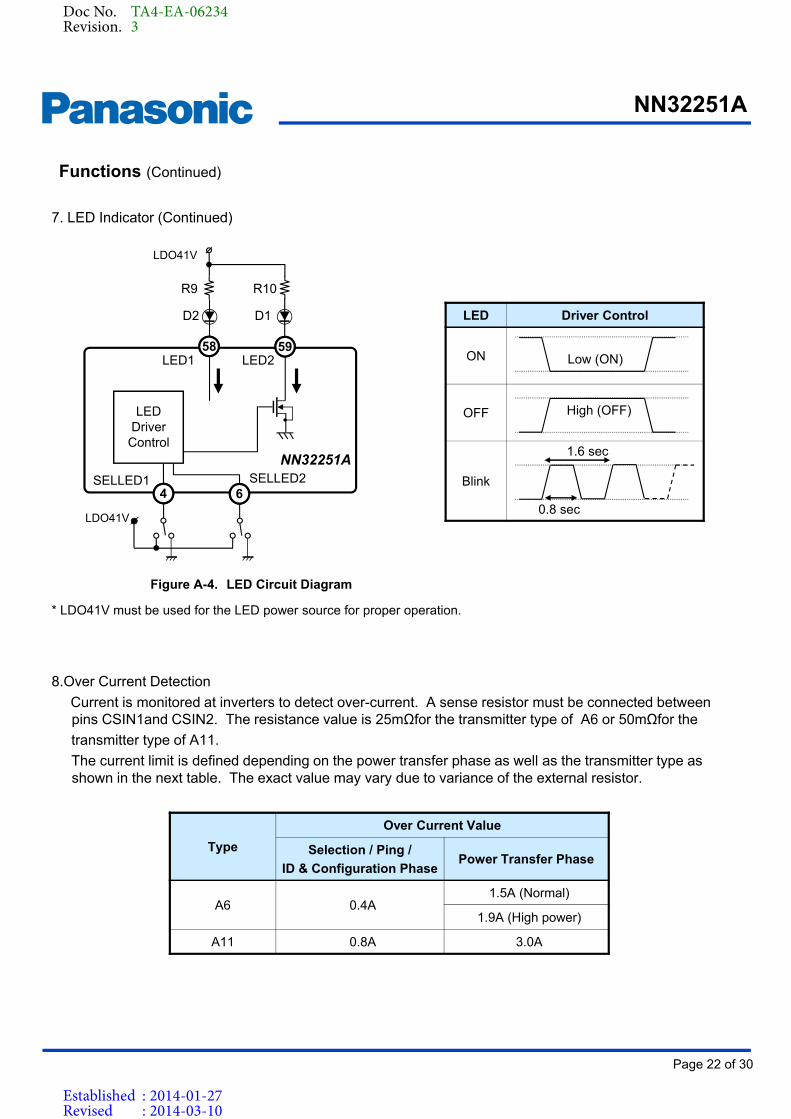
7. LED Indicator
NN32251A controls two LED’s, and the following colors are recommended to be used.
Functions (Continued)
The LED display pattern when the power is provided from AC adapter is shown below.
Pin Name(Number) LED
Pin
System Status
SelectionPing
ID & ConfigurationPower Transfer
Full ChargeError
Temperature Error
ChargeSELLED2
(No.6)SELLED1
(No.4) Standby Charge Full Charge Error
GND GNDLED1 OFF ON OFF Blink*1
LED2 OFF OFF ON OFF
GND LDO41VLED1 OFF OFF OFF ON
LED2 OFF Blink*1 ON OFF
LDO41V GNDLED1 ON OFF OFF ON
LED2 ON Blink*1 ON OFF
LDO41V LDO41VLED1 OFF OFF OFF ON
LED2 OFF ON OFF OFF
When the supply voltage decreases, by such reasons as not-enough current from an AC adaptor,
the LED pattern in charge status starts and goes back to the above power-on sequence, and then
it repeats.
Power On form AC adaptor
Pin LED display
LED1
(RED)
LED2
(Green)
0.5 sec
ON OFF ON
OFF ON ON
Combination of LED display can be adjusted by pins SELLED1(No.4) and SELLED2(No.6) as
the next table shows.
Pin Name LED1 LED2
Number No.58 No.59
LED Color Red Green
*1 Blinking frequency = 0.625Hz
0.5 sec0.5 sec
0.5 sec
Doc No. TA4-EA-06234Revision. 3
Established : 2014-01-27Revised : 2014-03-10
Page 22 of 30
NN32251A
Product Standards
LED Driver Control
ON
OFF
Blink
7. LED Indicator (Continued)
Low (ON)
High (OFF)
1.6 sec
0.8 sec
8.Over Current Detection
Current is monitored at inverters to detect over-current. A sense resistor must be connected between pins CSIN1and CSIN2. The resistance value is 25mΩfor the transmitter type of A6 or 50mΩfor the
transmitter type of A11.
The current limit is defined depending on the power transfer phase as well as the transmitter type as shown in the next table. The exact value may vary due to variance of the external resistor.
Functions (Continued)
Figure A-4. LED Circuit Diagram
R9 R10
D2 D1
LED1 LED25958
LDO41V
NN32251ASELLED1 SELLED2
64
LDO41V
LEDDriver
Control
Type
Over Current Value
Selection / Ping /
ID & Configuration PhasePower Transfer Phase
A6 0.4A1.5A (Normal)
1.9A (High power)
A11 0.8A 3.0A
* LDO41V must be used for the LED power source for proper operation.
Doc No. TA4-EA-06234Revision. 3
Established : 2014-01-27Revised : 2014-03-10

Page 23 of 30
NN32251A
Product Standards
9. Over Temperature Protection
NN32251A has three pins (TH1, TH2, and TH3) to connect thermistors.
A thermistor (NXRT15XH103FA3A016 recommended) is inserted into R6, R8, or R12, and the detecting
temperatures are adjusted by the values of remaining resistors. Power transfer stops when a temperature
becomes over a specified value.
For example, when NXRT15XH103FA3A016 is used for the pin TH1, and power transfer needs to be
stopped over 65 and restarted under 60 (with ±2 accuracy), the following resistor values may be
used; R13: 10kohm±1%, R18: 10kohm±1%, and R19: 38.3kohm±1%.
The detecting voltages, then, will be 0.641V for stopping power transfer and 0.719V for restarting it.
In order to inactivate this function, connect the pins TH1, TH2, and TH3 to LDO33V.
LDO41V
R12
R7
R14
R15
TH
1
TH
2
TH
3
R8
R11
R16
R17
R6
R13
R18
R19
Temp.Monitor
202122
NN32251A 12bits ADC
図A-5. Over-Temperature Detection
Functions (Continued)
LDO33V
TH
1
TH
2
TH
3
NN32251A 12bits ADC
(a) Active circuit (b) The function is inactivated
Temp.Monitor
202122
Doc No. TA4-EA-06234Revision. 3
Established : 2014-01-27Revised : 2014-03-10
Page 24 of 30
NN32251A
Product Standards
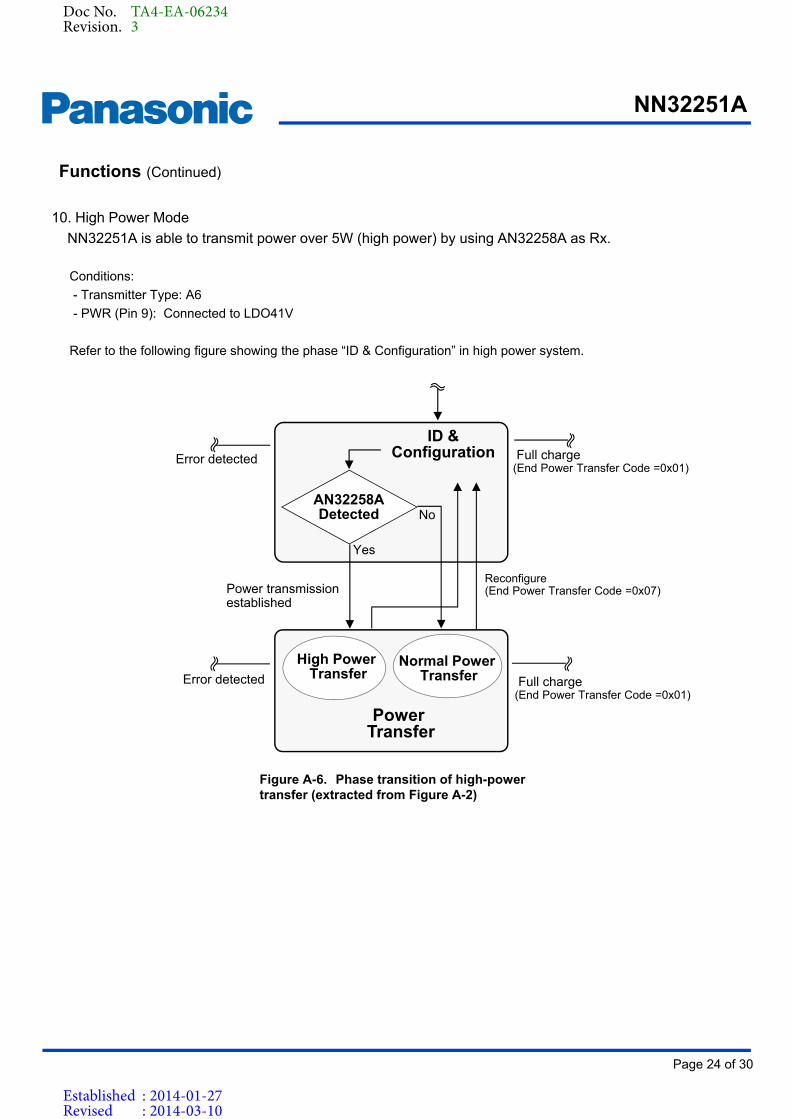
10. High Power Mode
NN32251A is able to transmit power over 5W (high power) by using AN32258A as Rx.
Conditions:
- Transmitter Type: A6
- PWR (Pin 9): Connected to LDO41V
Refer to the following figure showing the phase “ID & Configuration” in high power system.
ID & Configuration
Power Transfer
Error detected
AN32258ADetected
High Power Transfer
Normal Power Transfer
Yes
No
Figure A-6. Phase transition of high-power transfer (extracted from Figure A-2)
Functions (Continued)
Full charge(End Power Transfer Code =0x01)
Power transmissionestablished
Error detected
Reconfigure(End Power Transfer Code =0x07)
Full charge(End Power Transfer Code =0x01)
Doc No. TA4-EA-06234Revision. 3
Established : 2014-01-27Revised : 2014-03-10

Page 25 of 30
NN32251A
Product Standards
LDO
41V
Cur
rent
Sen
se
Res
isto
r
Pow
er S
uppl
y (5
.0V
)
EN
B C
on
tro
l3.
3V:a
ctiv
e0V
:res
et
LDO
33V
D3L2
A11 (0
.1u
F*4
)
Q5
Q7
R2 1k
R3 10k
C3
3300
pF
C4
1000
pF
C5
6800
0pF
C202200pF
Opt
iona
l T
herm
isto
r
LDO
41V
R9
560
R10
560
D2
D1
R12
R7 R14 R15
C8
1uF
C71000pF
C62200pF
C24
10u
FC
4210
uF
VADP
LED1
LED2
VREF
TY
P1 G
ND
MC
SM
BD
MO
DE
TH1
TH2
TH3
LDO41V
CSIN1
CSIN2
VMODIN
VFIL1
VFIL2
LDO18V
CFIL1
CFIL2
PD
1H
PD
1L
PD
2H
PD
2L
PD
3L
PD
3H
PD
4L
PD
4H
GNDA1
GNDP1GNDP2
TEST
GN
DA
3
LDO33V
GNDMOD
SM
BC
NC
O1
NC
O2
PW
R
FW
MD
TE
ST
2
EN
B
VFIL3
VFIL4
PLLFIL
CSOUT
CMODIN
TE
ST
4
SC
DE
T1
SC
DE
T2
SC
DE
T3
SC
DE
T4
VIN
V
HG
1
LG1
HG
2
LG2
CFB1
CFB2
VFB
C18C28C29
R8
R11 R16 R17
R6
R13 R18 R19
C9
1uF
C10
4.7u
FC
111u
FC
1239
00p
FC
1310
00p
FC
1433
00p
F
C15
10u
FC
160.
01u
F
C23
10u
F
60 15 6 5 4 2 3
20
21
22
1
24
18
19
23
25
26
27
28
29
30
42
31
4846454744433640393538374155535149
64
17
59
58
34
16
33
32
50
54
52
61
57
56
62 6313 12 11 10 9 8 714
NN32251A
IC1
EVALUATION RESULTS
Evaluation Circuit Diagram 1Conditions :
Tx Type: A11, Single coilADP (Pin 50): 5V inputENB (Pin 15): Connected to LDO33VTYP1(Pin 5) :Connected to GNDPWR (Pin 9): Connected to GNDRx:AN32258A evaluation board
Figure B-1. Circuit diagram for type A11 with a single coilC19
0.01uF
SE
LLE
D2
SE
LFO
D1
SE
LFO
D2
SE
LLE
D1
C30R4
25m
Q6
Q8
6.3u
H
LDO
41V
Doc No. TA4-EA-06234Revision. 3
Established : 2014-01-27Revised : 2014-03-10
Page 26 of 30
NN32251A
Product Standards
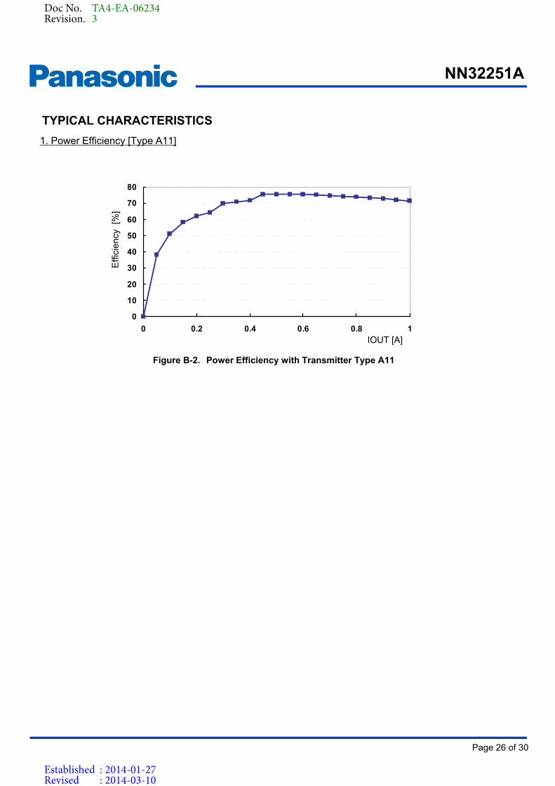
1. Power Efficiency [Type A11]
Figure B-2. Power Efficiency with Transmitter Type A11
Effi
cien
cy [
%]
IOUT [A]
TYPICAL CHARACTERISTICS
0
10
20
30
40
50
60
70
80
0 0.2 0.4 0.6 0.8 1
Doc No. TA4-EA-06234Revision. 3
Established : 2014-01-27Revised : 2014-03-10
Page 27 of 30
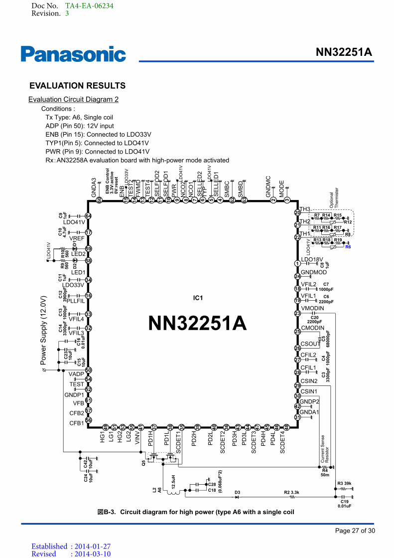
NN32251A
Product Standards
Cur
rent
Sen
se
Res
isto
r
Pow
er S
uppl
y (1
2.0V
)
EN
B C
on
tro
l3.
3V:a
ctiv
e0V
:res
et
LDO
33V
C3
3300
pF
C4
1000
pF
C5
6800
0pF
C202200pF
Opt
iona
l T
herm
iste
r
LDO
41V
R9
560
R10
560
D2
D1
R12
R7 R14 R15
C8
1uF
C71000pF
C62200pF
VADP
LED1
LED2
VREF
TY
P1 G
ND
MC
SM
BD
MO
DE
TH1
TH2
TH3
LDO41V
CSIN1
CSIN2
VMODIN
VFIL1
VFIL2
LDO18V
CFIL1
CFIL2
PD
1H
PD
1L
PD
2H
PD
2L
PD
3L
PD
3H
PD
4L
PD
4H
GNDA1
GNDP1GNDP2
TEST
GN
DA
3
LDO33V
GNDMOD
SM
BC
NC
O1
NC
O2
PW
R
FW
MD
TE
ST
2
EN
B
VFIL3
VFIL4
PLLFIL
CSOUT
CMODIN
TE
ST
4
SC
DE
T1
SC
DE
T2
SC
DE
T3
SC
DE
T4
VIN
V
HG
1
LG1
HG
2
LG2
CFB1
CFB2
VFB
R8
R11 R16 R17
R6
R13 R18 R19
C9
1uF
C10
4.7u
FC
111u
FC
1239
00p
FC
1310
00p
FC
1433
00p
F
C15
10u
FC
160.
01u
F
C23
10u
F
60 15 6 5 4 2 3
20
21
22
1
24
18
19
23
25
26
27
28
29
30
42
31
4846454744433640393538374155535149
64
17
59
58
34
16
33
32
50
54
52
61
57
56
62 6313 12 11 10 9 8 714
図B-3. Circuit diagram for high power (type A6 with a single coil
NN32251A
IC1
LDO
41V
LDO
41V
EVALUATION RESULTS
Evaluation Circuit Diagram 2Conditions :
Tx Type: A6, Single coilADP (Pin 50): 12V inputENB (Pin 15): Connected to LDO33VTYP1(Pin 5): Connected to LDO41VPWR (Pin 9): Connected to LDO41VRx:AN32258A evaluation board with high-power mode activated
SE
LLE
D2
SE
LFO
D1
SE
LFO
D2
SE
LLE
D1
LDO
41V
D3L2
A6
(0.0
68u
F*2
)
Q5
R2 3.3k
C190.01uF
R3 39k
R450m
C24
10u
FC
4210
uF
C18C28
12.5
uH
Doc No. TA4-EA-06234Revision. 3
Established : 2014-01-27Revised : 2014-03-10

Page 28 of 30
NN32251A
Product Standards
0
10
20
30
40
50
60
70
80
0 500 1000 1500 2000
Effi
cien
cy [
%]
IOUT [mA]
2. Power Efficiency [High Power, Type A6]
TYPICAL CHARACTERISTICS
Figure B-4. Power Efficiency with AN32258A, High Power, and Transmitter Type A6
Doc No. TA4-EA-06234Revision. 3
Established : 2014-01-27Revised : 2014-03-10
Page 29 of 30
NN32251A
Product Standards
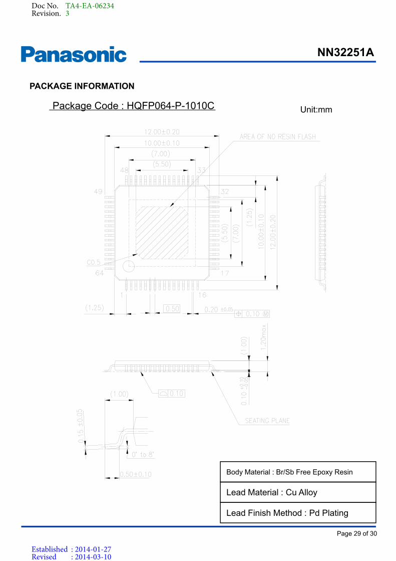
Unit:mmPackage Code : HQFP064-P-1010C
Lead Finish Method : Pd Plating
Lead Material : Cu Alloy
Body Material : Br/Sb Free Epoxy Resin
PACKAGE INFORMATION
Doc No. TA4-EA-06234Revision. 3
Established : 2014-01-27Revised : 2014-03-10

Page 30 of 30
NN32251A
Product Standards
IMPORTANT NOTICE
1. When using the IC for new models, verify the safety including the long-term reliability for each product.
2. When the application system is designed by using this IC, please confirm the notes in this book. Please read the notes to descriptions and the usage notes in the book.
3. This IC is intended to be used for general electronic equipment.Consult our sales staff in advance for information on the following applications: Special applications in which exceptional quality and reliability are required, or if the failure or malfunction of this IC may directly jeopardize life or harm the human body.Any applications other than the standard applications intended.
(1) Space appliance (such as artificial satellite, and rocket)(2) Traffic control equipment (such as for automotive, airplane, train, and ship)(3) Medical equipment for life support(4) Submarine transponder(5) Control equipment for power plant(6) Disaster prevention and security device(7) Weapon(8) Others : Applications of which reliability equivalent to (1) to (7) is required
Our company shall not be held responsible for any damage incurred as a result of or in connection with the IC being used for any special application, unless our company agrees to the use of such special application.However, for the IC which we designate as products for automotive use, it is possible to be used for automotive.
4. This IC is neither designed nor intended for use in automotive applications or environments unless the IC is designated by our company to be used in automotive applications.
Our company shall not be held responsible for any damage incurred by customers or any third party as a result of or in connection with the IC being used in automotive application, unless our company agrees to such application in this book.
5. Please use this IC in compliance with all applicable laws and regulations that regulate the inclusion or use of controlled substances, including without limitation, the EU RoHS Directive. Our company shall not be held responsible for any damage incurred as a result of our IC being used by our customers, not complying with the applicable laws and regulations.
6. Pay attention to the direction of the IC. When mounting it in the wrong direction onto the PCB (printed-circuit-board), it might be damaged.
7. Pay attention in the PCB (printed-circuit-board) pattern layout in order to prevent damage due to short circuit between pins. In addition, refer to the Pin Description for the pin configuration.
8. Perform visual inspection on the PCB before applying power, otherwise damage might happen due to problems such as solder-bridge between the pins of the IC. Also, perform full technical verification on the assembly quality, because the same damage possibly can happen due to conductive substances, such as solder ball, that adhere to the IC during transportation.
9. Take notice in the use of this IC that it might be damaged when an abnormal state occurs such as output pin-VCC short (Power supply fault), output pin-GND short (Ground fault), or output-to-output-pin short (load short). Safety measures such as installation of fuses are recommended because the extent of the above-mentioned damage will depend on the current capability of the power supply.
10. The protection circuit is for maintaining safety against abnormal operation. Therefore, the protection circuit should not work during normal operation.Especially for the thermal protection circuit, if the area of safe operation or the absolute maximum rating is momentarily exceeded due to output pin to VCC short (Power supply fault), or output pin to GND short (Ground fault), the IC might be damaged before the thermal protection circuit could operate.
11. Unless specified in the product specifications, make sure that negative voltage or excessive voltage are not applied to the pins because the IC might be damaged, which could happen due to negative voltage or excessive voltage generated during the ON and OFF timing when the inductive load of a motor coil or actuator coils of optical pick-up is being driven.
12. Verify the risks which might be caused by the malfunctions of external components.
Doc No. TA4-EA-06234Revision. 3
Established : 2014-01-27Revised : 2014-03-10

Request for your special attention and precautions in using the technical information andsemiconductors described in this book
(1) If any of the products or technical information described in this book is to be exported or provided to non-residents, the laws and regulations of the exporting country, especially, those with regard to security export control, must be observed.
(2) The technical information described in this book is intended only to show the main characteristics and application circuit examples of the products. No license is granted in and to any intellectual property right or other right owned by Panasonic Corporation or any other company. Therefore, no responsibility is assumed by our company as to the infringement upon any such right owned by any other company which may arise as a result of the use of technical information described in this book.
(3) The products described in this book are intended to be used for general applications (such as office equipment, communications equipment, measuring instruments and household appliances), or for specific applications as expressly stated in this book.Consult our sales staff in advance for information on the following applications: Special applications (such as for airplanes, aerospace, automotive equipment, traffic signaling equipment, combustion equipment,
life support systems and safety devices) in which exceptional quality and reliability are required, or if the failure or malfunction of the products may directly jeopardize life or harm the human body.
It is to be understood that our company shall not be held responsible for any damage incurred as a result of or in connection with your using the products described in this book for any special application, unless our company agrees to your using the products in this book for any special application.
(4) The products and product specifications described in this book are subject to change without notice for modification and/or im-provement. At the final stage of your design, purchasing, or use of the products, therefore, ask for the most up-to-date Product Standards in advance to make sure that the latest specifications satisfy your requirements.
(5) When designing your equipment, comply with the range of absolute maximum rating and the guaranteed operating conditions (operating power supply voltage and operating environment etc.). Especially, please be careful not to exceed the range of absolute maximum rating on the transient state, such as power-on, power-off and mode-switching. Otherwise, we will not be liable for any defect which may arise later in your equipment.
Even when the products are used within the guaranteed values, take into the consideration of incidence of break down and failure mode, possible to occur to semiconductor products. Measures on the systems such as redundant design, arresting the spread of fire or preventing glitch are recommended in order to prevent physical injury, fire, social damages, for example, by using the products.
(6) Comply with the instructions for use in order to prevent breakdown and characteristics change due to external factors (ESD, EOS, thermal stress and mechanical stress) at the time of handling, mounting or at customer's process. When using products for which damp-proof packing is required, satisfy the conditions, such as shelf life and the elapsed time since first opening the packages.
(7) This book may be not reprinted or reproduced whether wholly or partially, without the prior written permission of our company.
20100202