NDeRC Nanotechnology Collaboration Introduction
15
NANO Collaboration Molecular Nano-electronics
-
Upload
tom-loughran -
Category
Technology
-
view
557 -
download
3
Transcript of NDeRC Nanotechnology Collaboration Introduction

NANO Collaboration
Molecular Nano-electronics
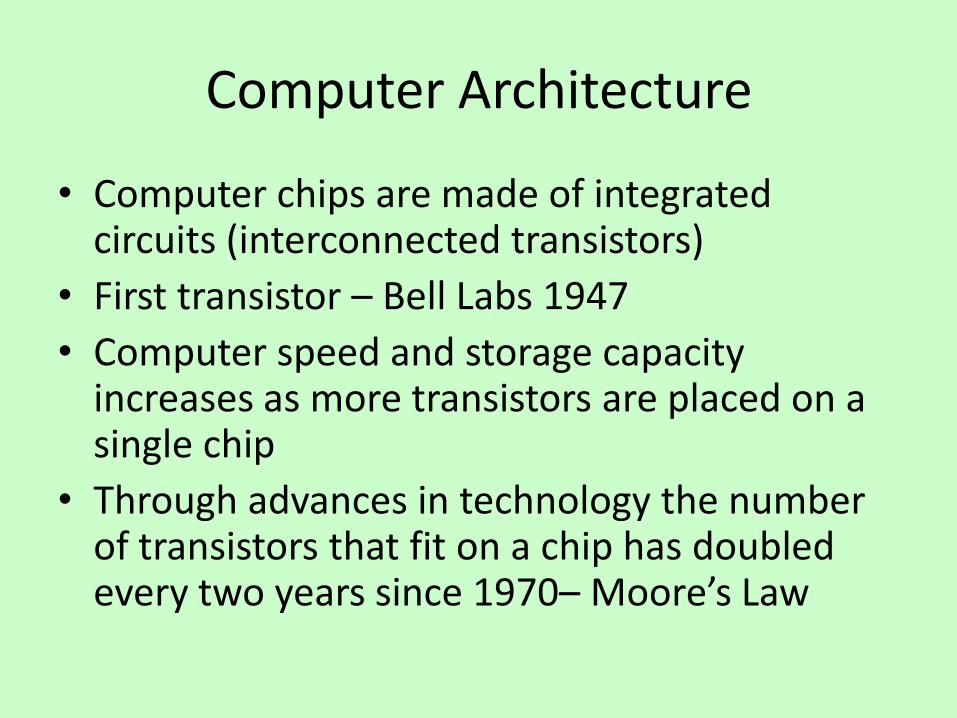
Computer Architecture
• Computer chips are made of integrated circuits (interconnected transistors)
• First transistor – Bell Labs 1947
• Computer speed and storage capacity increases as more transistors are placed on a single chip
• Through advances in technology the number of transistors that fit on a chip has doubled every two years since 1970– Moore’s Law

Moore’s Law

Limits of Current Technology
• Etching or cutting structures in semiconductors may be reaching a size limit: immersion lithography 45nm (too large)
• Semiconductor devices generate a lot of heat – even large cooling systems that are used today won’t be able to cool fast enough as the transistors get still smaller (packed more densely) and the heat/volume increases – the devices will melt
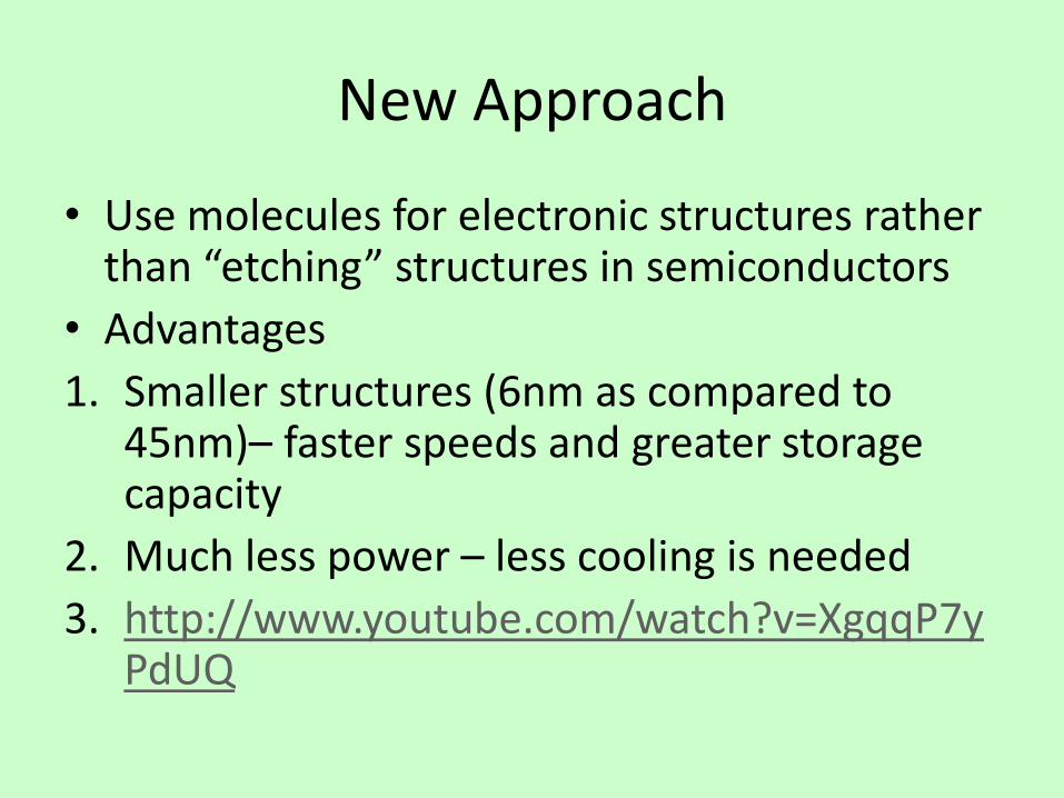
New Approach
• Use molecules for electronic structures rather than “etching” structures in semiconductors
• Advantages
1. Smaller structures (6nm as compared to 45nm)– faster speeds and greater storage capacity
2. Much less power – less cooling is needed
3. http://www.youtube.com/watch?v=XgqqP7yPdUQ

Molecular Structures
• We would like:
1.Self assembly – structures “build themselves”
Taken by
Song Guo
In
Dr. Alex
Kandel’s Lab
On a Low
Temperature
UHV STM
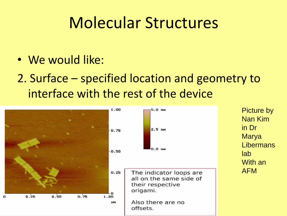
Molecular Structures
• We would like:
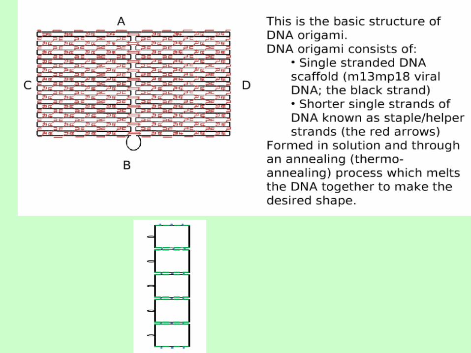
2. Surface – specified location and geometry to interface with the rest of the device
– DNA Tiling: DNA Origami Picture by
Nan Kim
in Dr
Marya
Libermans
lab
With an
AFM
Molecular Structures
• We would like:
2. Surface – specified location and geometry to interface with the rest of the device
• Surface chemistry to assemble structures

Molecular Structures
• We would like:
2. Surface – specified location and geometry to interface with the rest of the device
• Scanning probe microscopes to see/measure features of the molecular structure

Portable STM and Cool Temperature UHV STM

Molecular Structures
• We would like:
1. Self assembly – structures “build themselves”
2. Surface – specified location and geometry to interface with the rest of the device
• DNA Tiling: DNA Origami
• Surface chemistry to assemble structures
• Scanning probe microscopes to see/measure features of the molecular structure
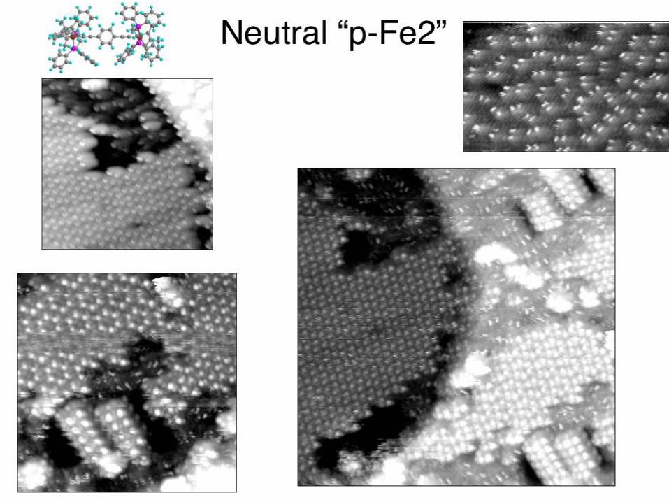
This summer I am working with Dr. Alex Kandel , the graduate students
In his lab– Rebecca Quardokus and Annette Raigoza., and a high school
Student.
We the studying the effects of alpha particle radiation on the surface of Gold
that has a self assembled monolayer of octothiol.
We hope to find out not only what happens to the surface, but how large an
area Is af effected and the preferred amount of time to get optimum results.
The ultimate goal is to be able to use the alpha particles to help map the chip
Or to use it to sharpen the tips of our STM so we can sharpen the tip without
Removing it from the machine.