
MIXED SIGNAL MICROCONTROLLER - Elektronik...
44
MSP430G2x31 MSP430G2x21 www.ti.com SLAS694E – FEBRUARY 2010 – REVISED JANUARY 2011 MIXED SIGNAL MICROCONTROLLER 1FEATURES • Low Supply-Voltage Range: 1.8 V to 3.6 V • 16-Bit Timer_A With Two Capture/Compare Registers • Ultra-Low Power Consumption • Universal Serial Interface (USI) Supporting SPI – Active Mode: 220 μA at 1 MHz, 2.2 V and I2C (See Table 1) – Standby Mode: 0.5 μA • Brownout Detector – Off Mode (RAM Retention): 0.1 μA • 10-Bit 200-ksps A/D Converter With Internal • Five Power-Saving Modes Reference, Sample-and-Hold, and Autoscan • Ultra-Fast Wake-Up From Standby Mode in (See Table 1) Less Than 1 μs • Serial Onboard Programming, • 16-Bit RISC Architecture, 62.5-ns Instruction No External Programming Voltage Needed, Cycle Time Programmable Code Protection by Security • Basic Clock Module Configurations Fuse – Internal Frequencies up to 16 MHz With • On-Chip Emulation Logic With Spy-Bi-Wire One Calibrated Frequency Interface – Internal Very Low Power Low-Frequency • Family Members Details See Table 1 (LF) Oscillator • Available in 14-Pin Plastic Small-Outline Thin – 32-kHz Crystal Package (TSSOP), 14-Pin Plastic Dual Inline – External Digital Clock Source Package (PDIP), and 16-Pin QFN • For Complete Module Descriptions, See the MSP430x2xx Family User’s Guide (SLAU144) DESCRIPTION The Texas Instruments MSP430 family of ultra-low-power microcontrollers consists of several devices featuring different sets of peripherals targeted for various applications. The architecture, combined with five low-power modes, is optimized to achieve extended battery life in portable measurement applications. The device features a powerful 16-bit RISC CPU, 16-bit registers, and constant generators that contribute to maximum code efficiency. The digitally controlled oscillator (DCO) allows wake-up from low-power modes to active mode in less than 1 μs. The MSP430G2x21/31 series is an ultralow-power mixed signal microcontroller with a built-in 16-bit timer and ten I/O pins. The MSP430G2x31 family members have a 10-bit A/D converter and built-in communication capability using synchronous protocols (SPI or I2C). For configuration details, see Table 1. Typical applications include low-cost sensor systems that capture analog signals, convert them to digital values, and then process the data for display or for transmission to a host system. 1 Please be aware that an important notice concerning availability, standard warranty, and use in critical applications of Texas Instruments semiconductor products and disclaimers thereto appears at the end of this data sheet. PRODUCTION DATA information is current as of publication date. Copyright © 2010–2011, Texas Instruments Incorporated Products conform to specifications per the terms of the Texas Instruments standard warranty. Production processing does not necessarily include testing of all parameters.
Transcript of MIXED SIGNAL MICROCONTROLLER - Elektronik...
MSP430G2x31MSP430G2x21
www.ti.com SLAS694E –FEBRUARY 2010–REVISED JANUARY 2011
MIXED SIGNAL MICROCONTROLLER
1FEATURES• Low Supply-Voltage Range: 1.8 V to 3.6 V • 16-Bit Timer_A With Two Capture/Compare
Registers• Ultra-Low Power Consumption• Universal Serial Interface (USI) Supporting SPI– Active Mode: 220 µA at 1 MHz, 2.2 V
and I2C (See Table 1)– Standby Mode: 0.5 µA• Brownout Detector– Off Mode (RAM Retention): 0.1 µA• 10-Bit 200-ksps A/D Converter With Internal• Five Power-Saving Modes
Reference, Sample-and-Hold, and Autoscan• Ultra-Fast Wake-Up From Standby Mode in (See Table 1)
Less Than 1 µs• Serial Onboard Programming,
• 16-Bit RISC Architecture, 62.5-ns Instruction No External Programming Voltage Needed,Cycle Time Programmable Code Protection by Security
• Basic Clock Module Configurations Fuse– Internal Frequencies up to 16 MHz With • On-Chip Emulation Logic With Spy-Bi-Wire
One Calibrated Frequency Interface– Internal Very Low Power Low-Frequency • Family Members Details See Table 1
(LF) Oscillator • Available in 14-Pin Plastic Small-Outline Thin– 32-kHz Crystal Package (TSSOP), 14-Pin Plastic Dual Inline– External Digital Clock Source Package (PDIP), and 16-Pin QFN
• For Complete Module Descriptions, See theMSP430x2xx Family User’s Guide (SLAU144)
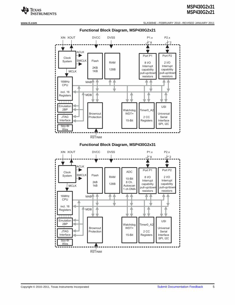
DESCRIPTIONThe Texas Instruments MSP430 family of ultra-low-power microcontrollers consists of several devices featuringdifferent sets of peripherals targeted for various applications. The architecture, combined with five low-powermodes, is optimized to achieve extended battery life in portable measurement applications. The device features apowerful 16-bit RISC CPU, 16-bit registers, and constant generators that contribute to maximum code efficiency.The digitally controlled oscillator (DCO) allows wake-up from low-power modes to active mode in less than 1 µs.
The MSP430G2x21/31 series is an ultralow-power mixed signal microcontroller with a built-in 16-bit timer and tenI/O pins. The MSP430G2x31 family members have a 10-bit A/D converter and built-in communication capabilityusing synchronous protocols (SPI or I2C). For configuration details, see Table 1.
Typical applications include low-cost sensor systems that capture analog signals, convert them to digital values,and then process the data for display or for transmission to a host system.
1
Please be aware that an important notice concerning availability, standard warranty, and use in critical applications of TexasInstruments semiconductor products and disclaimers thereto appears at the end of this data sheet.
PRODUCTION DATA information is current as of publication date. Copyright © 2010–2011, Texas Instruments IncorporatedProducts conform to specifications per the terms of the TexasInstruments standard warranty. Production processing does notnecessarily include testing of all parameters.

MSP430G2x31MSP430G2x21
SLAS694E –FEBRUARY 2010–REVISED JANUARY 2011 www.ti.com
Table 1. Available Options (1)
Flash RAM ADC10 PackageDevice BSL EEM Timer_A USI Clock I/O(KB) (B) Channel Type (2)
MSP430G2231IRSA16 16-QFNMSP430G2231IPW14 - 1 2 128 1x TA2 1 8 LF, DCO, VLO 10 14-TSSOPMSP430G2231IN14 14-PDIP
MSP430G2221IRSA16 16-QFNMSP430G2221IPW14 - 1 2 128 1x TA2 1 - LF, DCO, VLO 10 14-TSSOPMSP430G2221IN14 14-PDIP
MSP430G2131IRSA16 16-QFNMSP430G2131IPW14 - 1 1 128 1x TA2 1 8 LF, DCO, VLO 10 14-TSSOPMSP430G2131IN14 14-PDIP
MSP430G2121IRSA16 16-QFNMSP430G2121IPW14 - 1 1 128 1x TA2 1 - LF, DCO, VLO 10 14-TSSOPMSP430G2121IN14 14-PDIP
(1) For the most current package and ordering information, see the Package Option Addendum at the end of this document, or see the TIweb site at www.ti.com.
(2) Package drawings, thermal data, and symbolization are available at www.ti.com/packaging.
2 Submit Documentation Feedback Copyright © 2010–2011, Texas Instruments Incorporated

1DVCC
2
3
4
5
6
7 8 P1.6/TA0.1/SDO/SCL/TDI/TCLK
9 P1.7/SDI/SDA/TDO/TDI
10 RST/NMI/SBWTDIO
11 TEST/SBWTCK
12 XOUT/P2.7
13 XIN/P2.6/TA0.1
14 DVSS
P1.0/TA0CLK/ACLK
P1.1/TA0.0
P1.2/TA0.1
P1.3
P1.4/SMCLK/TCK
P1.5/TA0.0/SCLK/TMS
N OR PW PACKAGE(TOP VIEW)
1
2
3
4
5
P1.4
/SM
CLK
/TC
K
6
P1.5
/TA
0.0
/SC
LK
/TM
S
7
P1.6
/TA
0.1
/SD
O/S
CL/T
DI/T
CLK
8
P1.7
/SD
I/S
DA
/TD
O/T
DI
9
10
11
12
13
DV
SS
14D
VS
S15
DV
CC
16
DV
CC
P1.0/TA0CLK/ACLK
P1.1/TA0.0
P1.2/TA0.1
P1.3
RSA PACKAGE(TOP VIEW)
XIN/P2.6/TA0.1
XOUT/P2.7
TEST/SBWTCK
RST/NMI/SBWTDIO
MSP430G2x31MSP430G2x21
www.ti.com SLAS694E –FEBRUARY 2010–REVISED JANUARY 2011
Device Pinout, MSP430G2x21
NOTE: See port schematics in Application Information for detailed I/O information.
NOTE: See port schematics in Application Information for detailed I/O information.
Copyright © 2010–2011, Texas Instruments Incorporated Submit Documentation Feedback 3

1DVCC
2
3
4
5
6
7 8 P1.6/TA0.1/A6/SDO/SCL/TDI/TCLK
9 P1.7/A7/SDI/SDA/TDO/TDI
10 RST/NMI/SBWTDIO
11 TEST/SBWTCK
12 XOUT/P2.7
13 XIN/P2.6/TA0.1
14 DVSS
P1.0/TA0CLK/ACLK/A0
P1.1/TA0.0/A1
P1.2/TA0.1/A2
P1.3/ADC10CLK/A3/VREF-/VEREF-
P1.4/SMCLK/A4/VREF+/VEREF+/TCK
P1.5/TA0.0/A5/SCLK/TMS
N OR PW PACKAGE(TOP VIEW)
1
2
3
4
5
P1.4
/SM
CL
K/A
4/V
RE
F+
/VE
RE
F+
/TC
K
6
P1
.5/T
A0
.0/S
CLK
/A5/T
MS
7
P1
.6/T
A0.1
/SD
O/S
CL
/TD
I/T
CL
K
8P
1.7
/SD
I/S
DA
/TD
O/T
DI
9 RST/NMI/SBWTDIO
10 TEST/SBWTCK
11 XOUT/P2.7
12 XIN/P2.6/TA0.1
13
DV
SS
14
DV
SS
15
DV
CC
16
DV
CC
P1.0/TA0CLK/ACLK/A0
P1.1/TA0.0/A1
P1.2/TA0.1/A2
P1.3/ADC10CLK/A3/VREF-/VEREF-
RSA PACKAGE(TOP VIEW)
MSP430G2x31MSP430G2x21
SLAS694E –FEBRUARY 2010–REVISED JANUARY 2011 www.ti.com
Device Pinout, MSP430G2x31
NOTE: See port schematics in Application Information for detailed I/O information.
NOTE: See port schematics in Application Information for detailed I/O information.
4 Submit Documentation Feedback Copyright © 2010–2011, Texas Instruments Incorporated
Clock
System
Brownout
Protection
RST/NMI
DVCC DVSS
MCLK
Watchdog
WDT+
15-Bit
Timer0_A2
2 CC
Registers
16MHz
CPU
incl. 16
Registers
Emulation
2BP
JTAG
Interface
SMCLK
ACLK
MDB
MAB
Port P1
8 I/O
Interrupt
capability
pull-up/down
resistors
P1.x
8
Spy-Bi
Wire
XIN XOUT
RAM
128B
Flash
2KB
1KB
P2.x
Port P2
2 I/O
Interrupt
capability
pull-up/down
resistors
2
USI
Universal
Serial
Interface
SPI, I2C
Clock
System
Brownout
Protection
RST/NMI
DVCC DVSS
MCLK
Watchdog
WDT+
15-Bit
Timer0_A2
2 CC
Registers
16MHz
CPU
incl. 16
Registers
Emulation
2BP
JTAG
Interface
SMCLK
ACLK
MDB
MAB
Port P1
8 I/O
Interrupt
capability
pull-up/down
resistors
P1.x
8
Spy-Bi
Wire
XIN XOUT
RAM
128B
Flash
2kB
1kB
ADC
10-Bit
8 Ch.
Autoscan
1 ch DMA
P2.x
Port P2
2 I/O
Interrupt
capability
pull-up/down
resistors
2
USI
Universal
Serial
Interface
SPI, I2C
MSP430G2x31MSP430G2x21
www.ti.com SLAS694E –FEBRUARY 2010–REVISED JANUARY 2011
Functional Block Diagram, MSP430G2x21
Functional Block Diagram, MSP430G2x31
Copyright © 2010–2011, Texas Instruments Incorporated Submit Documentation Feedback 5

MSP430G2x31MSP430G2x21
SLAS694E –FEBRUARY 2010–REVISED JANUARY 2011 www.ti.com
Table 2. Terminal Functions
TERMINAL
NO. I/O DESCRIPTIONNAME 14 16
N, PW RSA
P1.0/ General-purpose digital I/O pinTA0CLK/ Timer0_A, clock signal TACLK input2 1 I/OACLK/ ACLK signal outputA0 ADC10 analog input A0 (1)
P1.1/ General-purpose digital I/O pinTA0.0/ 3 2 I/O Timer0_A, capture: CCI0A input, compare: Out0 outputA1 ADC10 analog input A1 (1)
P1.2/ General-purpose digital I/O pinTA0.1/ 4 3 I/O Timer0_A, capture: CCI1A input, compare: Out1 outputA2 ADC10 analog input A2 (1)
P1.3/ General-purpose digital I/O pinADC10CLK/ ADC10, conversion clock output (1)
5 4 I/OA3/ ADC10 analog input A3 (1)
VREF-/VEREF ADC10 negative reference voltage (1)
P1.4/ General-purpose digital I/O pinSMCLK/ SMCLK signal outputA4/ 6 5 I/O ADC10 analog input A4 (1)
VREF+/VEREF+/ ADC10 positive reference voltage (1)
TCK JTAG test clock, input terminal for device programming and test
P1.5/ General-purpose digital I/O pinTA0.0/ Timer0_A, compare: Out0 outputA5/ 7 6 I/O ADC10 analog input A5 (1)
SCLK/ USI: clock input in I2C mode; clock input/output in SPI modeTMS JTAG test mode select, input terminal for device programming and test
P1.6/ General-purpose digital I/O pinTA0.1/ Timer0_A, compare: Out1 outputA6/ ADC10 analog input A6 (1)
8 7 I/OSDO/ USI: Data output in SPI modeSCL/ USI: I2C clock in I2C modeTDI/TCLK JTAG test data input or test clock input during programming and test
P1.7/ General-purpose digital I/O pinA7/ ADC10 analog input A7 (1)
SDI/ 9 8 I/O USI: Data input in SPI modeSDA/ USI: I2C data in I2C modeTDO/TDI (2) JTAG test data output terminal or test data input during programming and test
XIN/ Input terminal of crystal oscillatorP2.6/ 13 12 I/O General-purpose digital I/O pinTA0.1 Timer0_A, compare: Out1 output
XOUT/ Output terminal of crystal oscillator (3)12 11 I/OP2.7 General-purpose digital I/O pin
RST/ ResetNMI/ 10 9 I Nonmaskable interrupt inputSBWTDIO Spy-Bi-Wire test data input/output during programming and test
TEST/ Selects test mode for JTAG pins on Port 1. The device protection fuse is connected to TEST.11 10 ISBWTCK Spy-Bi-Wire test clock input during programming and test
DVCC 1 15, 16 NA Supply voltage
DVSS 14 13, 14 NA Ground reference
QFN Pad - Pad NA QFN package pad connection to VSS recommended.
(1) MSP430G2x31 only(2) TDO or TDI is selected via JTAG instruction.(3) If XOUT/P2.7 is used as an input, excess current will flow until P2SEL.7 is cleared. This is due to the oscillator output driver connection
to this pad after reset.
6 Submit Documentation Feedback Copyright © 2010–2011, Texas Instruments Incorporated

Program Counter PC/R0
Stack Pointer SP/R1
Status Register SR/CG1/R2
Constant Generator CG2/R3
General-Purpose Register R4
General-Purpose Register R5
General-Purpose Register R6
General-Purpose Register R7
General-Purpose Register R8
General-Purpose Register R9
General-Purpose Register R10
General-Purpose Register R11
General-Purpose Register R12
General-Purpose Register R13
General-Purpose Register R15
General-Purpose Register R14
MSP430G2x31MSP430G2x21
www.ti.com SLAS694E –FEBRUARY 2010–REVISED JANUARY 2011
SHORT-FORM DESCRIPTION
CPUThe MSP430 CPU has a 16-bit RISC architecturethat is highly transparent to the application. Alloperations, other than program-flow instructions, areperformed as register operations in conjunction withseven addressing modes for source operand and fouraddressing modes for destination operand.
The CPU is integrated with 16 registers that providereduced instruction execution time. Theregister-to-register operation execution time is onecycle of the CPU clock.
Four of the registers, R0 to R3, are dedicated asprogram counter, stack pointer, status register, andconstant generator, respectively. The remainingregisters are general-purpose registers.
Peripherals are connected to the CPU using data,address, and control buses, and can be handled withall instructions.
The instruction set consists of the original 51instructions with three formats and seven addressmodes and additional instructions for the expandedaddress range. Each instruction can operate on wordand byte data.
Instruction Set
The instruction set consists of 51 instructions withthree formats and seven address modes. Eachinstruction can operate on word and byte data.Table 3 shows examples of the three types ofinstruction formats; Table 4 shows the addressmodes.
Table 3. Instruction Word Formats
Dual operands, source-destination e.g., ADD R4,R5 R4 + R5 ---> R5
Single operands, destination only e.g., CALL R8 PC -->(TOS), R8--> PC
Relative jump, un/conditional e.g., JNE Jump-on-equal bit = 0
Table 4. Address Mode Descriptions (1)
ADDRESS MODE S D SYNTAX EXAMPLE OPERATION
Register MOV Rs,Rd MOV R10,R11 R10 -- --> R11
Indexed MOV X(Rn),Y(Rm) MOV 2(R5),6(R6) M(2+R5) -- --> M(6+R6)
Symbolic (PC relative) MOV EDE,TONI M(EDE) -- --> M(TONI)
Absolute MOV &MEM,&TCDAT M(MEM) -- --> M(TCDAT)
Indirect MOV @Rn,Y(Rm) MOV @R10,Tab(R6) M(R10) -- --> M(Tab+R6)
M(R10) -- --> R11Indirect autoincrement MOV @Rn+,Rm MOV @R10+,R11 R10 + 2-- --> R10
Immediate MOV #X,TONI MOV #45,TONI #45 -- --> M(TONI)
(1) S = source, D = destination
Copyright © 2010–2011, Texas Instruments Incorporated Submit Documentation Feedback 7

MSP430G2x31MSP430G2x21
SLAS694E –FEBRUARY 2010–REVISED JANUARY 2011 www.ti.com
Operating Modes
The MSP430 has one active mode and five software selectable low-power modes of operation. An interruptevent can wake up the device from any of the low-power modes, service the request, and restore back to thelow-power mode on return from the interrupt program.
The following six operating modes can be configured by software:• Active mode (AM)
– All clocks are active• Low-power mode 0 (LPM0)
– CPU is disabled– ACLK and SMCLK remain active, MCLK is disabled
• Low-power mode 1 (LPM1)– CPU is disabled– ACLK and SMCLK remain active, MCLK is disabled– DCO's dc generator is disabled if DCO not used in active mode
• Low-power mode 2 (LPM2)– CPU is disabled– MCLK and SMCLK are disabled– DCO's dc generator remains enabled– ACLK remains active
• Low-power mode 3 (LPM3)– CPU is disabled– MCLK and SMCLK are disabled– DCO's dc generator is disabled– ACLK remains active
• Low-power mode 4 (LPM4)– CPU is disabled– ACLK is disabled– MCLK and SMCLK are disabled– DCO's dc generator is disabled– Crystal oscillator is stopped
8 Submit Documentation Feedback Copyright © 2010–2011, Texas Instruments Incorporated

MSP430G2x31MSP430G2x21
www.ti.com SLAS694E –FEBRUARY 2010–REVISED JANUARY 2011
Interrupt Vector Addresses
The interrupt vectors and the power-up starting address are located in the address range 0FFFFh to 0FFC0h.The vector contains the 16-bit address of the appropriate interrupt handler instruction sequence.
If the reset vector (located at address 0FFFEh) contains 0FFFFh (e.g., flash is not programmed) the CPU will gointo LPM4 immediately after power-up.
Table 5. Interrupt Sources, Flags, and Vectors
SYSTEM WORDINTERRUPT SOURCE INTERRUPT FLAG PRIORITYINTERRUPT ADDRESS
Power-Up PORIFGExternal Reset RSTIFG
Watchdog Timer+ WDTIFG Reset 0FFFEh 31, highestFlash key violation KEYV (2)
PC out-of-range (1)
NMI NMIIFG (non)-maskableOscillator fault OFIFG (non)-maskable 0FFFCh 30
Flash memory access violation ACCVIFG (2) (3) (non)-maskable
0FFFAh 29
0FFF8h 28
0FFF6h 27
Watchdog Timer+ WDTIFG maskable 0FFF4h 26
Timer_A2 TACCR0 CCIFG (4) maskable 0FFF2h 25
Timer_A2 TACCR1 CCIFG, TAIFG (2) (4) maskable 0FFF0h 24
0FFEEh 23
0FFECh 22
ADC10 (5) ADC10IFG (4) (5) maskable 0FFEAh 21
USI USIIFG, USISTTIFG (2) (4) maskable 0FFE8h 20
I/O Port P2 (two flags) P2IFG.6 to P2IFG.7 (2) (4) maskable 0FFE6h 19
I/O Port P1 (eight flags) P1IFG.0 to P1IFG.7 (2) (4) maskable 0FFE4h 18
0FFE2h 17
0FFE0h 16
See (6) 0FFDEh to 15 to 0, lowest0FFC0h
(1) A reset is generated if the CPU tries to fetch instructions from within the module register memory address range (0h to 01FFh) or fromwithin unused address ranges.
(2) Multiple source flags(3) (non)-maskable: the individual interrupt-enable bit can disable an interrupt event, but the general interrupt enable cannot.(4) Interrupt flags are located in the module.(5) MSP430G2x31 only(6) The interrupt vectors at addresses 0FFDEh to 0FFC0h are not used in this device and can be used for regular program code if
necessary.
Copyright © 2010–2011, Texas Instruments Incorporated Submit Documentation Feedback 9

MSP430G2x31MSP430G2x21
SLAS694E –FEBRUARY 2010–REVISED JANUARY 2011 www.ti.com
Special Function Registers (SFRs)
Most interrupt and module enable bits are collected into the lowest address space. Special function register bitsnot allocated to a functional purpose are not physically present in the device. Simple software access is providedwith this arrangement.
Legend rw: Bit can be read and written.
rw-0,1: Bit can be read and written. It is reset or set by PUC.
rw-(0,1): Bit can be read and written. It is reset or set by POR.
SFR bit is not present in device.
Table 6. Interrupt Enable Register 1 and 2Address 7 6 5 4 3 2 1 0
00h ACCVIE NMIIE OFIE WDTIE
rw-0 rw-0 rw-0 rw-0
WDTIE Watchdog Timer interrupt enable. Inactive if watchdog mode is selected. Active if Watchdog Timer is configured ininterval timer mode.
OFIE Oscillator fault interrupt enable
NMIIE (Non)maskable interrupt enable
ACCVIE Flash access violation interrupt enable
Address 7 6 5 4 3 2 1 0
01h
Table 7. Interrupt Flag Register 1 and 2Address 7 6 5 4 3 2 1 0
02h NMIIFG RSTIFG PORIFG OFIFG WDTIFG
rw-0 rw-(0) rw-(1) rw-1 rw-(0)
WDTIFG Set on watchdog timer overflow (in watchdog mode) or security key violation.Reset on VCC power-on or a reset condition at the RST/NMI pin in reset mode.
OFIFG Flag set on oscillator fault.
PORIFG Power-On Reset interrupt flag. Set on VCC power-up.
RSTIFG External reset interrupt flag. Set on a reset condition at RST/NMI pin in reset mode. Reset on VCC power-up.
NMIIFG Set via RST/NMI pin
Address 7 6 5 4 3 2 1 0
03h
10 Submit Documentation Feedback Copyright © 2010–2011, Texas Instruments Incorporated
MSP430G2x31MSP430G2x21
www.ti.com SLAS694E –FEBRUARY 2010–REVISED JANUARY 2011
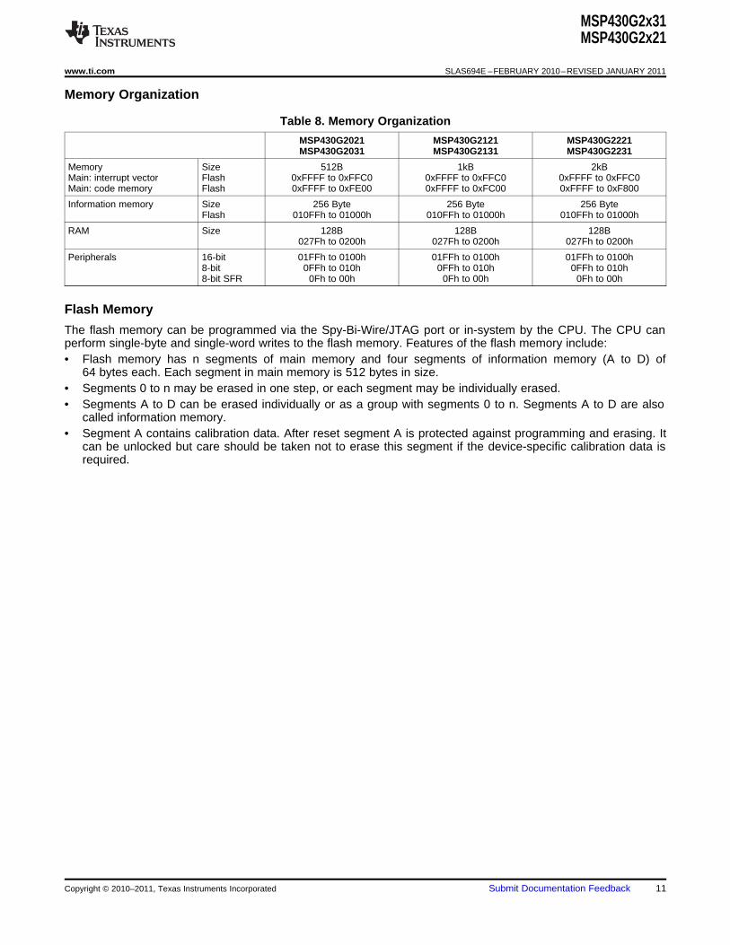
Memory Organization
Table 8. Memory Organization
MSP430G2021 MSP430G2121 MSP430G2221MSP430G2031 MSP430G2131 MSP430G2231
Memory Size 512B 1kB 2kBMain: interrupt vector Flash 0xFFFF to 0xFFC0 0xFFFF to 0xFFC0 0xFFFF to 0xFFC0Main: code memory Flash 0xFFFF to 0xFE00 0xFFFF to 0xFC00 0xFFFF to 0xF800
Information memory Size 256 Byte 256 Byte 256 ByteFlash 010FFh to 01000h 010FFh to 01000h 010FFh to 01000h
RAM Size 128B 128B 128B027Fh to 0200h 027Fh to 0200h 027Fh to 0200h
Peripherals 16-bit 01FFh to 0100h 01FFh to 0100h 01FFh to 0100h8-bit 0FFh to 010h 0FFh to 010h 0FFh to 010h8-bit SFR 0Fh to 00h 0Fh to 00h 0Fh to 00h
Flash Memory
The flash memory can be programmed via the Spy-Bi-Wire/JTAG port or in-system by the CPU. The CPU canperform single-byte and single-word writes to the flash memory. Features of the flash memory include:• Flash memory has n segments of main memory and four segments of information memory (A to D) of
64 bytes each. Each segment in main memory is 512 bytes in size.• Segments 0 to n may be erased in one step, or each segment may be individually erased.• Segments A to D can be erased individually or as a group with segments 0 to n. Segments A to D are also
called information memory.• Segment A contains calibration data. After reset segment A is protected against programming and erasing. It
can be unlocked but care should be taken not to erase this segment if the device-specific calibration data isrequired.
Copyright © 2010–2011, Texas Instruments Incorporated Submit Documentation Feedback 11

MSP430G2x31MSP430G2x21
SLAS694E –FEBRUARY 2010–REVISED JANUARY 2011 www.ti.com
Peripherals
Peripherals are connected to the CPU through data, address, and control buses and can be handled using allinstructions. For complete module descriptions, see the MSP430x2xx Family User's Guide (SLAU144).
Oscillator and System Clock
The clock system is supported by the basic clock module that includes support for a 32768-Hz watch crystaloscillator, an internal very-low-power low-frequency oscillator and an internal digitally controlled oscillator (DCO).The basic clock module is designed to meet the requirements of both low system cost and low powerconsumption. The internal DCO provides a fast turn-on clock source and stabilizes in less than 1µs. The basicclock module provides the following clock signals:• Auxiliary clock (ACLK), sourced either from a 32768-Hz watch crystal or the internal LF oscillator.• Main clock (MCLK), the system clock used by the CPU.• Sub-Main clock (SMCLK), the sub-system clock used by the peripheral modules.
Table 9. DCO Calibration Data(Provided From Factory In Flash Information Memory Segment A)
CALIBRATIONDCO FREQUENCY SIZE ADDRESSREGISTER
CALBC1_1MHZ byte 010FFh1 MHz
CALDCO_1MHZ byte 010FEh
Brownout
The brownout circuit is implemented to provide the proper internal reset signal to the device during power on andpower off.
Digital I/O
There is one 8-bit I/O port implemented—port P1—and two bits of I/O port P2:• All individual I/O bits are independently programmable.• Any combination of input, output, and interrupt condition is possible.• Edge-selectable interrupt input capability for all the eight bits of port P1 and the two bits of port P2.• Read/write access to port-control registers is supported by all instructions.• Each I/O has an individually programmable pull-up/pull-down resistor.
WDT+ Watchdog Timer
The primary function of the watchdog timer (WDT+) module is to perform a controlled system restart after asoftware problem occurs. If the selected time interval expires, a system reset is generated. If the watchdogfunction is not needed in an application, the module can be disabled or configured as an interval timer and cangenerate interrupts at selected time intervals.
12 Submit Documentation Feedback Copyright © 2010–2011, Texas Instruments Incorporated

MSP430G2x31MSP430G2x21
www.ti.com SLAS694E –FEBRUARY 2010–REVISED JANUARY 2011
Timer_A2
Timer_A2 is a 16-bit timer/counter with two capture/compare registers. Timer_A2 can support multiplecapture/compares, PWM outputs, and interval timing. Timer_A2 also has extensive interrupt capabilities.Interrupts may be generated from the counter on overflow conditions and from each of the capture/compareregisters.
Table 10. Timer_A2 Signal Connections – Device With ADC10
INPUT PIN NUMBER MODULE OUTPUT PIN NUMBERDEVICE INPUT MODULE MODULE OUTPUTSIGNAL INPUT NAME BLOCKPW, N RSA PW, N RSASIGNAL
2 - P1.0 1 - P1.0 TACLK TACLK
ACLK ACLKTimer NA
SMCLK SMCLK
2 - P1.0 1 - P1.0 TACLK INCLK
3 - P1.1 2 - P1.1 TA0 CCI0A 3 - P1.1 2 - P1.1
ACLK (internal) CCI0B 7 - P1.5 6 - P1.5CCR0 TA0
VSS GND
VCC VCC
4 - P1.2 3 - P1.2 TA1 CCI1A 4 - P1.2 3 - P1.2
8 - P1.6 7 - P1.6 TA1 CCI1B 8 - P1.6 7 - P1.6CCR1 TA1
VSS GND 13 - P2.6 12 - P2.6
VCC VCC
USI
The universal serial interface (USI) module is used for serial data communication and provides the basichardware for synchronous communication protocols like SPI and I2C.
ADC10 (MSP430G2x31 only)
The ADC10 module supports fast, 10-bit analog-to-digital conversions. The module implements a 10-bit SARcore, sample select control, reference generator and data transfer controller, or DTC, for automatic conversionresult handling, allowing ADC samples to be converted and stored without any CPU intervention.
Copyright © 2010–2011, Texas Instruments Incorporated Submit Documentation Feedback 13
MSP430G2x31MSP430G2x21
SLAS694E –FEBRUARY 2010–REVISED JANUARY 2011 www.ti.com
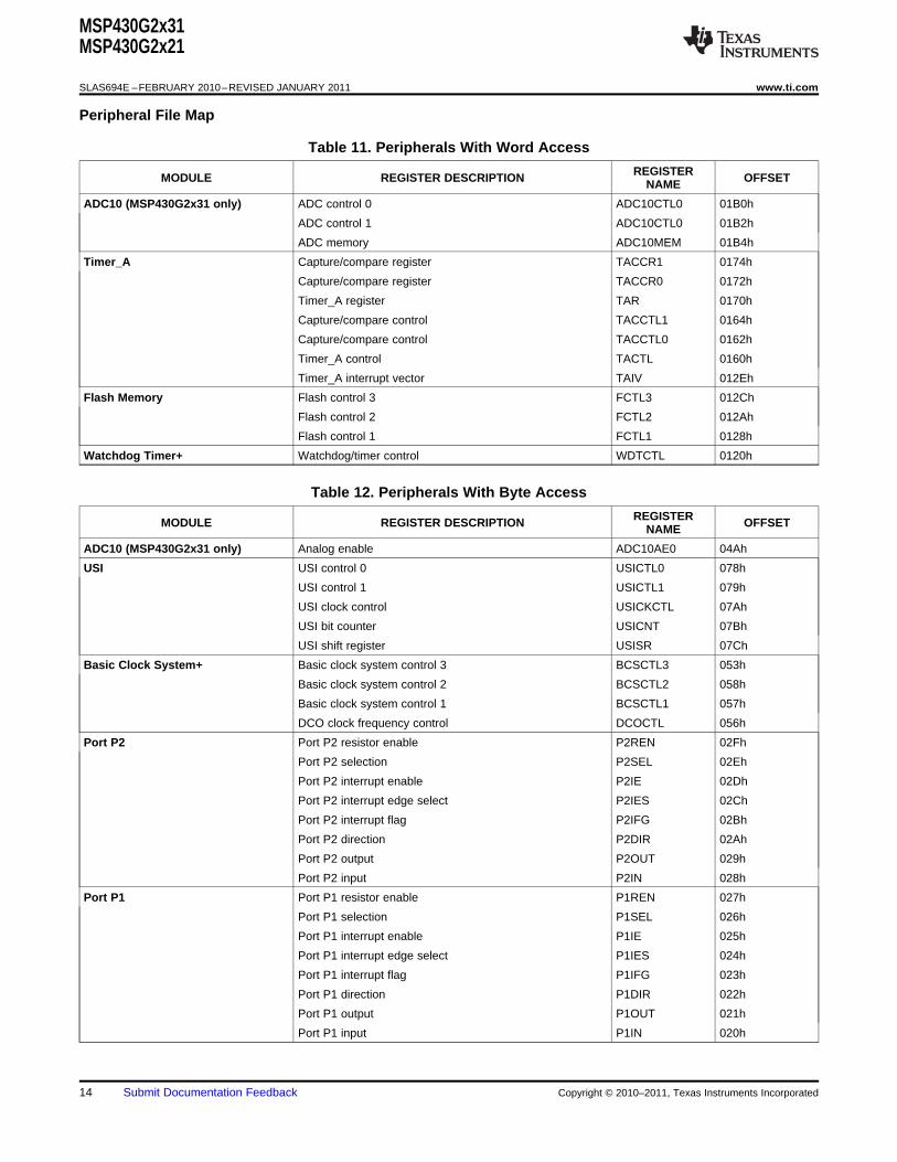
Peripheral File Map
Table 11. Peripherals With Word Access
REGISTERMODULE REGISTER DESCRIPTION OFFSETNAME
ADC10 (MSP430G2x31 only) ADC control 0 ADC10CTL0 01B0h
ADC control 1 ADC10CTL0 01B2h
ADC memory ADC10MEM 01B4h
Timer_A Capture/compare register TACCR1 0174h
Capture/compare register TACCR0 0172h
Timer_A register TAR 0170h
Capture/compare control TACCTL1 0164h
Capture/compare control TACCTL0 0162h
Timer_A control TACTL 0160h
Timer_A interrupt vector TAIV 012Eh
Flash Memory Flash control 3 FCTL3 012Ch
Flash control 2 FCTL2 012Ah
Flash control 1 FCTL1 0128h
Watchdog Timer+ Watchdog/timer control WDTCTL 0120h
Table 12. Peripherals With Byte Access
REGISTERMODULE REGISTER DESCRIPTION OFFSETNAME
ADC10 (MSP430G2x31 only) Analog enable ADC10AE0 04Ah
USI USI control 0 USICTL0 078h
USI control 1 USICTL1 079h
USI clock control USICKCTL 07Ah
USI bit counter USICNT 07Bh
USI shift register USISR 07Ch
Basic Clock System+ Basic clock system control 3 BCSCTL3 053h
Basic clock system control 2 BCSCTL2 058h
Basic clock system control 1 BCSCTL1 057h
DCO clock frequency control DCOCTL 056h
Port P2 Port P2 resistor enable P2REN 02Fh
Port P2 selection P2SEL 02Eh
Port P2 interrupt enable P2IE 02Dh
Port P2 interrupt edge select P2IES 02Ch
Port P2 interrupt flag P2IFG 02Bh
Port P2 direction P2DIR 02Ah
Port P2 output P2OUT 029h
Port P2 input P2IN 028h
Port P1 Port P1 resistor enable P1REN 027h
Port P1 selection P1SEL 026h
Port P1 interrupt enable P1IE 025h
Port P1 interrupt edge select P1IES 024h
Port P1 interrupt flag P1IFG 023h
Port P1 direction P1DIR 022h
Port P1 output P1OUT 021h
Port P1 input P1IN 020h
14 Submit Documentation Feedback Copyright © 2010–2011, Texas Instruments Incorporated

MSP430G2x31MSP430G2x21
www.ti.com SLAS694E –FEBRUARY 2010–REVISED JANUARY 2011
Table 12. Peripherals With Byte Access (continued)
REGISTERMODULE REGISTER DESCRIPTION OFFSETNAME
Special Function SFR interrupt flag 2 IFG2 003h
SFR interrupt flag 1 IFG1 002h
SFR interrupt enable 2 IE2 001h
SFR interrupt enable 1 IE1 000h
Copyright © 2010–2011, Texas Instruments Incorporated Submit Documentation Feedback 15
4.15 MHz
12 MHz
16 MHz
1.8 V 2.2 V 2.7 V 3.3 V 3.6 V
Supply Voltage −V
Syste
mF
requency
−M
Hz
Supply voltage rangeduring flash memoryprogramming
Supply voltage rangeduring program execution
Legend:
7.5 MHz
MSP430G2x31MSP430G2x21
SLAS694E –FEBRUARY 2010–REVISED JANUARY 2011 www.ti.com
Absolute Maximum Ratings (1)
Voltage applied at VCC to VSS –0.3 V to 4.1 V
Voltage applied to any pin (2) –0.3 V to VCC + 0.3 V
Diode current at any device pin ±2 mA
Unprogrammed device –55°C to 150°CStorage temperature range, Tstg
(3)
Programmed device –40°C to 85°C
(1) Stresses beyond those listed under "absolute maximum ratings" may cause permanent damage to the device. These are stress ratingsonly, and functional operation of the device at these or any other conditions beyond those indicated under "recommended operatingconditions" is not implied. Exposure to absolute-maximum-rated conditions for extended periods may affect device reliability.
(2) All voltages referenced to VSS. The JTAG fuse-blow voltage, VFB, is allowed to exceed the absolute maximum rating. The voltage isapplied to the TEST pin when blowing the JTAG fuse.
(3) Higher temperature may be applied during board soldering according to the current JEDEC J-STD-020 specification with peak reflowtemperatures not higher than classified on the device label on the shipping boxes or reels.
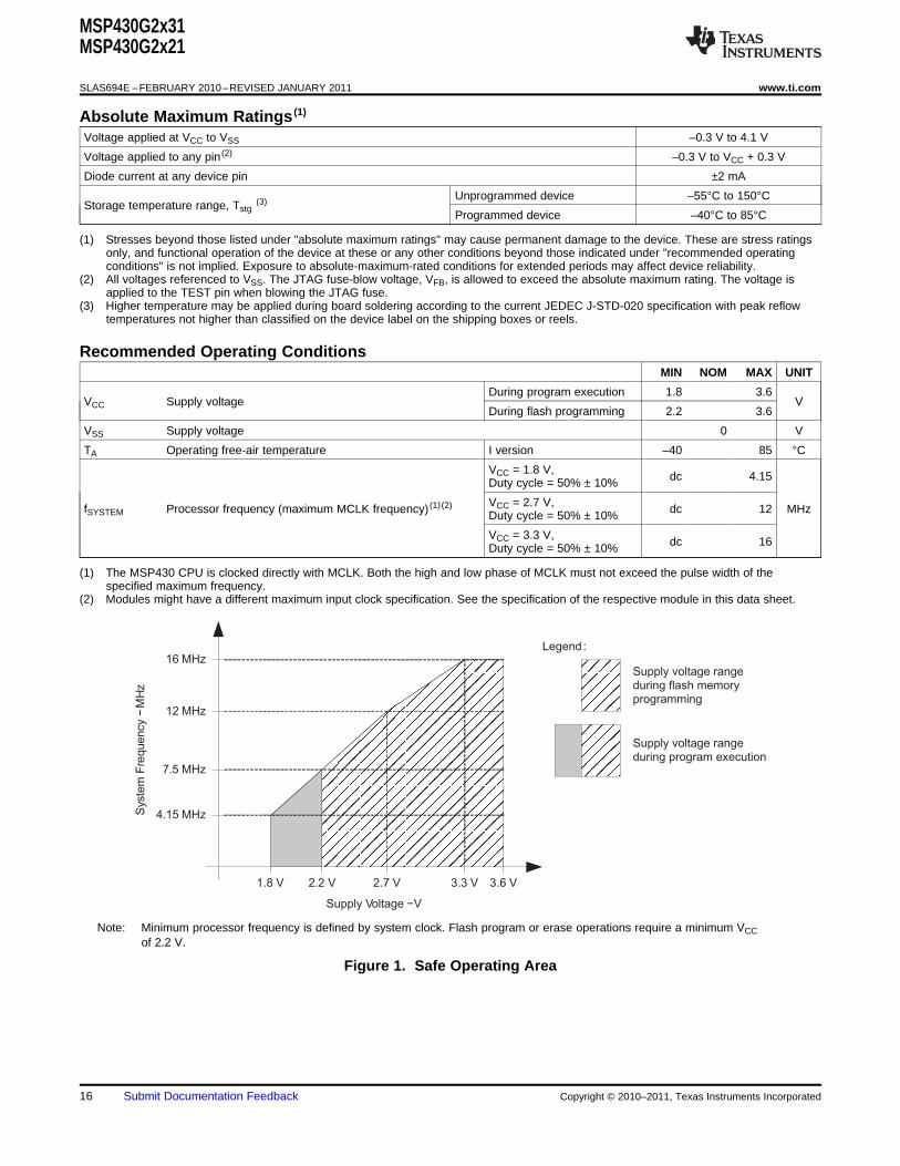
Recommended Operating ConditionsMIN NOM MAX UNIT
During program execution 1.8 3.6VCC Supply voltage V
During flash programming 2.2 3.6
VSS Supply voltage 0 V
TA Operating free-air temperature I version –40 85 °C
VCC = 1.8 V, dc 4.15Duty cycle = 50% ± 10%
VCC = 2.7 V,fSYSTEM Processor frequency (maximum MCLK frequency) (1) (2) dc 12 MHzDuty cycle = 50% ± 10%
VCC = 3.3 V, dc 16Duty cycle = 50% ± 10%
(1) The MSP430 CPU is clocked directly with MCLK. Both the high and low phase of MCLK must not exceed the pulse width of thespecified maximum frequency.
(2) Modules might have a different maximum input clock specification. See the specification of the respective module in this data sheet.
Note: Minimum processor frequency is defined by system clock. Flash program or erase operations require a minimum VCCof 2.2 V.
Figure 1. Safe Operating Area
16 Submit Documentation Feedback Copyright © 2010–2011, Texas Instruments Incorporated

0.0
1.0
2.0
3.0
4.0
5.0
1.5 2.0 2.5 3.0 3.5 4.0
VCC − Supply Voltage − V
Active
Mo
de
Cu
rre
nt
−m
A
fDCO = 1 MHz
fDCO = 8 MHz
fDCO = 12 MHz
fDCO = 16 MHz
0.0
1.0
2.0
3.0
4.0
0.0 4.0 8.0 12.0 16.0
fDCO − DCO Frequency − MHz
Active
Mo
de
Cu
rre
nt
−m
A
TA = 25 °C
TA = 85 °C
VCC = 2.2 V
VCC = 3 V
TA = 25 °C
TA = 85 °C
MSP430G2x31MSP430G2x21
www.ti.com SLAS694E –FEBRUARY 2010–REVISED JANUARY 2011
Electrical Characteristics
Active Mode Supply Current Into VCC Excluding External Currentover recommended ranges of supply voltage and operating free-air temperature (unless otherwise noted) (1) (2)
PARAMETER TEST CONDITIONS TA VCC MIN TYP MAX UNIT
fDCO = fMCLK = fSMCLK = 1 MHz, 2.2 V 220fACLK = 32768 Hz,Program executes in flash,Active mode (AM)IAM,1MHz BCSCTL1 = CALBC1_1MHZ, µAcurrent (1 MHz) 3 V 300 370DCOCTL = CALDCO_1MHZ,CPUOFF = 0, SCG0 = 0, SCG1 = 0,OSCOFF = 0
(1) All inputs are tied to 0 V or to VCC. Outputs do not source or sink any current.(2) The currents are characterized with a Micro Crystal CC4V-T1A SMD crystal with a load capacitance of 9 pF. The internal and external
load capacitance is chosen to closely match the required 9 pF.Typical Characteristics – Active Mode Supply Current (Into VCC)
Figure 2. Active Mode Current vs VCC, TA = 25°C Figure 3. Active Mode Current vs DCO Frequency
Copyright © 2010–2011, Texas Instruments Incorporated Submit Documentation Feedback 17

0.00
0.25
0.50
0.75
1.00
1.25
1.50
1.75
2.00
2.25
2.50
-40
I–
Lo
w-P
ow
er
Mo
de C
urr
en
t–
µA
LP
M4
Vcc = 3.6 V
T – Temperature – °CA
Vcc = 1.8 V
Vcc = 3 V
Vcc = 2.2 V
-20 0 20 40 60 800.00
0.25
0.50
0.75
1.00
1.25
1.50
1.75
2.00
2.25
2.50
2.75
3.00
-40
I–
Lo
w-P
ow
er
Mo
de C
urr
en
t–
µA
LP
M3
Vcc = 3.6 V
T – Temperature – °CA
Vcc = 1.8 V
Vcc = 3 V
Vcc = 2.2 V
-20 0 20 40 60 80
MSP430G2x31MSP430G2x21
SLAS694E –FEBRUARY 2010–REVISED JANUARY 2011 www.ti.com
Low-Power Mode Supply Currents (Into VCC) Excluding External Currentover recommended ranges of supply voltage and operating free-air temperature (unless otherwise noted) (1) (2)
PARAMETER TEST CONDITIONS TA VCC MIN TYP MAX UNIT
fMCLK = 0 MHz,fSMCLK = fDCO = 1 MHz,fACLK = 32768 Hz,Low-power mode 0ILPM0,1MHz BCSCTL1 = CALBC1_1MHZ, 25°C 2.2 V 65 µA(LPM0) current (3)DCOCTL = CALDCO_1MHZ,CPUOFF = 1, SCG0 = 0, SCG1 = 0,OSCOFF = 0
fMCLK = fSMCLK = 0 MHz,fDCO = 1 MHz,fACLK = 32768 Hz,Low-power mode 2ILPM2 BCSCTL1 = CALBC1_1MHZ, 25°C 2.2 V 22 µA(LPM2) current (4)DCOCTL = CALDCO_1MHZ,CPUOFF = 1, SCG0 = 0, SCG1 = 1,OSCOFF = 0
fDCO = fMCLK = fSMCLK = 0 MHz,Low-power mode 3 fACLK = 32768 Hz,ILPM3,LFXT1 25°C 2.2 V 0.7 1.5 µA(LPM3) current (4) CPUOFF = 1, SCG0 = 1, SCG1 = 1,
OSCOFF = 0
fDCO = fMCLK = fSMCLK = 0 MHz,Low-power mode 3 fACLK from internal LF oscillator (VLO),ILPM3,VLO 25°C 2.2 V 0.5 0.7 µAcurrent, (LPM3) (4) CPUOFF = 1, SCG0 = 1, SCG1 = 1,
OSCOFF = 0
fDCO = fMCLK = fSMCLK = 0 MHz, 25°C 2.2 V 0.1 0.5 µALow-power mode 4 fACLK = 0 Hz,ILPM4 (LPM4) current (5) CPUOFF = 1, SCG0 = 1, SCG1 = 1, 85°C 2.2 V 0.8 1.5 µA
OSCOFF = 1
(1) All inputs are tied to 0 V or to VCC. Outputs do not source or sink any current.(2) The currents are characterized with a Micro Crystal CC4V-T1A SMD crystal with a load capacitance of 9 pF.(3) Current for brownout and WDT clocked by SMCLK included.(4) Current for brownout and WDT clocked by ACLK included.(5) Current for brownout included.
Typical Characteristics Low-Power Mode Supply Currentsover recommended ranges of supply voltage and operating free-air temperature (unless otherwise noted)
Figure 4. LPM3 Current vs Temperature Figure 5. LPM4 Current vs Temperature
18 Submit Documentation Feedback Copyright © 2010–2011, Texas Instruments Incorporated

MSP430G2x31MSP430G2x21
www.ti.com SLAS694E –FEBRUARY 2010–REVISED JANUARY 2011
Schmitt-Trigger Inputs – Ports Pxover recommended ranges of supply voltage and operating free-air temperature (unless otherwise noted)
PARAMETER TEST CONDITIONS VCC MIN TYP MAX UNIT
0.45 VCC 0.75 VCCVIT+ Positive-going input threshold voltage V
3 V 1.35 2.25
0.25 VCC 0.55 VCCVIT– Negative-going input threshold voltage V
3 V 0.75 1.65
Vhys Input voltage hysteresis (VIT+ – VIT–) 3 V 0.3 1 V
For pullup: VIN = VSSRPull Pullup/pulldown resistor 3 V 20 35 50 kΩFor pulldown: VIN = VCC
CI Input capacitance VIN = VSS or VCC 5 pF
Leakage Current – Ports Pxover recommended ranges of supply voltage and operating free-air temperature (unless otherwise noted)
PARAMETER TEST CONDITIONS VCC MIN MAX UNIT
Ilkg(Px.y) High-impedance leakage current (1) (2) 3 V ±50 nA
(1) The leakage current is measured with VSS or VCC applied to the corresponding pin(s), unless otherwise noted.(2) The leakage of the digital port pins is measured individually. The port pin is selected for input and the pullup/pulldown resistor is
disabled.
Outputs – Ports Pxover recommended ranges of supply voltage and operating free-air temperature (unless otherwise noted)
PARAMETER TEST CONDITIONS VCC MIN TYP MAX UNIT
VOH High-level output voltage I(OHmax) = –6 mA (1) 3 V VCC – 0.3 V
VOL Low-level output voltage I(OLmax) = 6 mA (1) 3 V VSS + 0.3 V
(1) The maximum total current, I(OHmax) and I(OLmax), for all outputs combined should not exceed ±48 mA to hold the maximum voltage dropspecified.
Output Frequency – Ports Pxover recommended ranges of supply voltage and operating free-air temperature (unless otherwise noted)
PARAMETER TEST CONDITIONS VCC MIN TYP MAX UNIT
Port output frequencyfPx.y Px.y, CL = 20 pF, RL = 1 kΩ (1) (2) 3 V 12 MHz(with load)
fPort_CLK Clock output frequency Px.y, CL = 20 pF (2) 3 V 16 MHz
(1) A resistive divider with 2 × 0.5 kΩ between VCC and VSS is used as load. The output is connected to the center tap of the divider.(2) The output voltage reaches at least 10% and 90% VCC at the specified toggle frequency.
Copyright © 2010–2011, Texas Instruments Incorporated Submit Documentation Feedback 19

VOL − Low-Level Output Voltage − V
0
5
10
15
20
25
30
0 0.5 1 1.5 2 2.5
VCC = 2.2 V
P1.7 TA = 25°C
TA = 85°C
OL
I−
Typ
ica
l L
ow
-Le
ve
l O
utp
ut
Cu
rre
nt
−m
A
VOL − Low-Level Output Voltage − V
0
10
20
30
40
50
0 0.5 1 1.5 2 2.5 3 3.5
VCC = 3 V
P1.7TA = 25°C
TA = 85°C
OL
I−
Typ
ica
l L
ow
-Le
ve
l O
utp
ut
Cu
rre
nt
−m
A
VOH − High-Level Output Voltage − V
−25
−20
−15
−10
−5
0
0 0.5 1 1.5 2 2.5
VCC = 2.2 V
P1.7
TA = 25°C
TA = 85°C
OH
I−
Typ
ica
l H
igh
-Le
ve
l O
utp
ut
Cu
rre
nt
−m
A
VOH − High-Level Output Voltage − V
−50
−40
−30
−20
−10
0
0 0.5 1 1.5 2 2.5 3 3.5
VCC = 3 V
P1.7
TA = 25°C
TA = 85°C
OH
I−
Typ
ica
l H
igh
-Le
ve
l O
utp
ut
Cu
rre
nt
−m
A
MSP430G2x31MSP430G2x21
SLAS694E –FEBRUARY 2010–REVISED JANUARY 2011 www.ti.com
Typical Characteristics – Outputsover recommended ranges of supply voltage and operating free-air temperature (unless otherwise noted)
TYPICAL LOW-LEVEL OUTPUT CURRENT TYPICAL LOW-LEVEL OUTPUT CURRENTvs vs
LOW-LEVEL OUTPUT VOLTAGE LOW-LEVEL OUTPUT VOLTAGE
Figure 6. Figure 7.
TYPICAL HIGH-LEVEL OUTPUT CURRENT TYPICAL HIGH-LEVEL OUTPUT CURRENTvs vs
HIGH-LEVEL OUTPUT VOLTAGE HIGH-LEVEL OUTPUT VOLTAGE
Figure 8. Figure 9.
20 Submit Documentation Feedback Copyright © 2010–2011, Texas Instruments Incorporated

0
1
t d(BOR)
VCC
V(B_IT−)
Vhys(B_IT−)
VCC(start)
MSP430G2x31MSP430G2x21
www.ti.com SLAS694E –FEBRUARY 2010–REVISED JANUARY 2011
POR/Brownout Reset (BOR) (1)
over recommended ranges of supply voltage and operating free-air temperature (unless otherwise noted)PARAMETER TEST CONDITIONS VCC MIN TYP MAX UNIT
VCC(start) See Figure 10 dVCC/dt ≤ 3 V/s 0.7 × V(B_IT–) V
V(B_IT–) See Figure 10 through Figure 12 dVCC/dt ≤ 3 V/s 1.35 V
Vhys(B_IT–) See Figure 10 dVCC/dt ≤ 3 V/s 140 mV
td(BOR) See Figure 10 2000 µs
Pulse length needed at RST/NMI pin tot(reset) 2.2 V/3 V 2 µsaccepted reset internally
(1) The current consumption of the brownout module is already included in the ICC current consumption data. The voltage level V(B_IT–) +Vhys(B_IT–)is ≤ 1.8 V.
Figure 10. POR/Brownout Reset (BOR) vs Supply Voltage
Copyright © 2010–2011, Texas Instruments Incorporated Submit Documentation Feedback 21

VCC(drop)
VCC
3 V
t pw
0
0.5
1
1.5
2
0.001 1 1000
Typical Conditions
1 ns 1 nstpw − Pulse Width − µs
VC
C(d
rop)
−V
tpw − Pulse Width − µs
VCC = 3 V
VCC
0
0.5
1
1.5
2
VCC(drop)
t pw
tpw − Pulse Width − µs
VC
C(d
rop)
−V
3 V
0.001 1 1000 tf tr
tpw − Pulse Width − µs
tf = tr
Typical Conditions
VCC = 3 V
MSP430G2x31MSP430G2x21
SLAS694E –FEBRUARY 2010–REVISED JANUARY 2011 www.ti.com
Typical Characteristics – POR/Brownout Reset (BOR)
Figure 11. VCC(drop) Level With a Square Voltage Drop to Generate a POR/Brownout Signal
Figure 12. VCC(drop) Level With a Triangle Voltage Drop to Generate a POR/Brownout Signal
22 Submit Documentation Feedback Copyright © 2010–2011, Texas Instruments Incorporated

DCO(RSEL,DCO+1)DCO(RSEL,DCO)average
DCO(RSEL,DCO) DCO(RSEL,DCO+1)
32 × f × ff =
MOD × f + (32 – MOD) × f
MSP430G2x31MSP430G2x21
www.ti.com SLAS694E –FEBRUARY 2010–REVISED JANUARY 2011
Main DCO Characteristics
• All ranges selected by RSELx overlap with RSELx + 1: RSELx = 0 overlaps RSELx = 1, ... RSELx = 14overlaps RSELx = 15.
• DCO control bits DCOx have a step size as defined by parameter SDCO.• Modulation control bits MODx select how often fDCO(RSEL,DCO+1) is used within the period of 32 DCOCLK
cycles. The frequency fDCO(RSEL,DCO) is used for the remaining cycles. The frequency is an average equal to:
DCO Frequencyover recommended ranges of supply voltage and operating free-air temperature (unless otherwise noted)
PARAMETER TEST CONDITIONS VCC MIN TYP MAX UNIT
RSELx < 14 1.8 3.6 V
VCC Supply voltage RSELx = 14 2.2 3.6 V
RSELx = 15 3 3.6 V
fDCO(0,0) DCO frequency (0, 0) RSELx = 0, DCOx = 0, MODx = 0 3 V 0.06 0.14 MHz
fDCO(0,3) DCO frequency (0, 3) RSELx = 0, DCOx = 3, MODx = 0 3 V 0.12 MHz
fDCO(1,3) DCO frequency (1, 3) RSELx = 1, DCOx = 3, MODx = 0 3 V 0.15 MHz
fDCO(2,3) DCO frequency (2, 3) RSELx = 2, DCOx = 3, MODx = 0 3 V 0.21 MHz
fDCO(3,3) DCO frequency (3, 3) RSELx = 3, DCOx = 3, MODx = 0 3 V 0.30 MHz
fDCO(4,3) DCO frequency (4, 3) RSELx = 4, DCOx = 3, MODx = 0 3 V 0.41 MHz
fDCO(5,3) DCO frequency (5, 3) RSELx = 5, DCOx = 3, MODx = 0 3 V 0.58 MHz
fDCO(6,3) DCO frequency (6, 3) RSELx = 6, DCOx = 3, MODx = 0 3 V 0.80 MHz
fDCO(7,3) DCO frequency (7, 3) RSELx = 7, DCOx = 3, MODx = 0 3 V 0.8 1.5 MHz
fDCO(8,3) DCO frequency (8, 3) RSELx = 8, DCOx = 3, MODx = 0 3 V 1.6 MHz
fDCO(9,3) DCO frequency (9, 3) RSELx = 9, DCOx = 3, MODx = 0 3 V 2.3 MHz
fDCO(10,3) DCO frequency (10, 3) RSELx = 10, DCOx = 3, MODx = 0 3 V 3.4 MHz
fDCO(11,3) DCO frequency (11, 3) RSELx = 11, DCOx = 3, MODx = 0 3 V 4.25 MHz
fDCO(12,3) DCO frequency (12, 3) RSELx = 12, DCOx = 3, MODx = 0 3 V 4.3 7.3 MHz
fDCO(13,3) DCO frequency (13, 3) RSELx = 13, DCOx = 3, MODx = 0 3 V 7.8 MHz
fDCO(14,3) DCO frequency (14, 3) RSELx = 14, DCOx = 3, MODx = 0 3 V 8.6 13.9 MHz
fDCO(15,3) DCO frequency (15, 3) RSELx = 15, DCOx = 3, MODx = 0 3 V 15.25 MHz
fDCO(15,7) DCO frequency (15, 7) RSELx = 15, DCOx = 7, MODx = 0 3 V 21 MHz
Frequency step betweenSRSEL SRSEL = fDCO(RSEL+1,DCO)/fDCO(RSEL,DCO) 3 V 1.35 ratiorange RSEL and RSEL+1
Frequency step betweenSDCO SDCO = fDCO(RSEL,DCO+1)/fDCO(RSEL,DCO) 3 V 1.08 ratiotap DCO and DCO+1
Duty cycle Measured at SMCLK output 3 V 50 %
Copyright © 2010–2011, Texas Instruments Incorporated Submit Documentation Feedback 23

DCO Frequency − MHz
0.10
1.00
10.00
0.10 1.00 10.00
DC
O W
ake
Tim
e−
µs
RSELx = 0...11RSELx = 12...15
MSP430G2x31MSP430G2x21
SLAS694E –FEBRUARY 2010–REVISED JANUARY 2011 www.ti.com
Calibrated DCO Frequencies – Toleranceover recommended ranges of supply voltage and operating free-air temperature (unless otherwise noted)
PARAMETER TEST CONDITIONS TA VCC MIN TYP MAX UNIT
BCSCTL1= CALBC1_1MHz,1-MHz tolerance over DCOCTL = CALDCO_1MHz, 0°C to 85°C 3 V -3 ±0.5 +3 %temperature (1)calibrated at 30°C and 3 V
BCSCTL1= CALBC1_1MHz,1-MHz tolerance over VCC DCOCTL = CALDCO_1MHz, 30°C 1.8 V to 3.6 V -3 ±2 +3 %
calibrated at 30°C and 3 V
BCSCTL1= CALBC1_1MHz,1-MHz tolerance overall DCOCTL = CALDCO_1MHz, -40°C to 85°C 1.8 V to 3.6 V -6 ±3 +6 %
calibrated at 30°C and 3 V
(1) This is the frequency change from the measured frequency at 30°C over temperature.
Wake-Up From Lower-Power Modes (LPM3/4) – Electrical Characteristicsover recommended ranges of supply voltage and operating free-air temperature (unless otherwise noted)
PARAMETER TEST CONDITIONS VCC MIN TYP MAX UNIT
DCO clock wake-up time from BCSCTL1= CALBC1_1MHz,tDCO,LPM3/4 3 V 1.5 µsLPM3/4 (1) DCOCTL = CALDCO_1MHz
1/fMCLK +tCPU,LPM3/4 CPU wake-up time from LPM3/4 (2)tClock,LPM3/4
(1) The DCO clock wake-up time is measured from the edge of an external wake-up signal (e.g., port interrupt) to the first clock edgeobservable externally on a clock pin (MCLK or SMCLK).
(2) Parameter applicable only if DCOCLK is used for MCLK.Typical Characteristics – DCO Clock Wake-Up Time From LPM3/4
Figure 13. DCO Wake-Up Time From LPM3 vs DCO Frequency
24 Submit Documentation Feedback Copyright © 2010–2011, Texas Instruments Incorporated
MSP430G2x31MSP430G2x21
www.ti.com SLAS694E –FEBRUARY 2010–REVISED JANUARY 2011
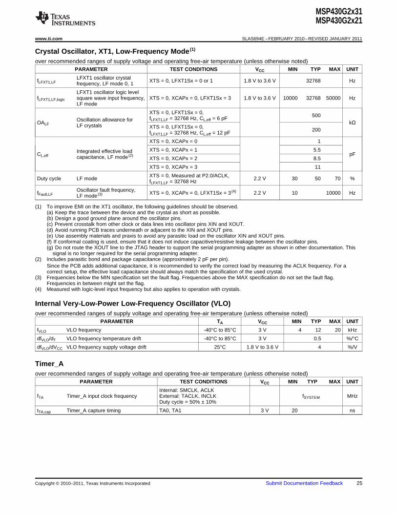
Crystal Oscillator, XT1, Low-Frequency Mode (1)
over recommended ranges of supply voltage and operating free-air temperature (unless otherwise noted)PARAMETER TEST CONDITIONS VCC MIN TYP MAX UNIT
LFXT1 oscillator crystalfLFXT1,LF XTS = 0, LFXT1Sx = 0 or 1 1.8 V to 3.6 V 32768 Hzfrequency, LF mode 0, 1
LFXT1 oscillator logic levelfLFXT1,LF,logic square wave input frequency, XTS = 0, XCAPx = 0, LFXT1Sx = 3 1.8 V to 3.6 V 10000 32768 50000 Hz
LF mode
XTS = 0, LFXT1Sx = 0, 500fLFXT1,LF = 32768 Hz, CL,eff = 6 pFOscillation allowance forOALF kΩLF crystals XTS = 0, LFXT1Sx = 0, 200fLFXT1,LF = 32768 Hz, CL,eff = 12 pF
XTS = 0, XCAPx = 0 1
XTS = 0, XCAPx = 1 5.5Integrated effective loadCL,eff pFcapacitance, LF mode (2)XTS = 0, XCAPx = 2 8.5
XTS = 0, XCAPx = 3 11
XTS = 0, Measured at P2.0/ACLK,Duty cycle LF mode 2.2 V 30 50 70 %fLFXT1,LF = 32768 Hz
Oscillator fault frequency,fFault,LF XTS = 0, XCAPx = 0, LFXT1Sx = 3 (4) 2.2 V 10 10000 HzLF mode (3)
(1) To improve EMI on the XT1 oscillator, the following guidelines should be observed.(a) Keep the trace between the device and the crystal as short as possible.(b) Design a good ground plane around the oscillator pins.(c) Prevent crosstalk from other clock or data lines into oscillator pins XIN and XOUT.(d) Avoid running PCB traces underneath or adjacent to the XIN and XOUT pins.(e) Use assembly materials and praxis to avoid any parasitic load on the oscillator XIN and XOUT pins.(f) If conformal coating is used, ensure that it does not induce capacitive/resistive leakage between the oscillator pins.(g) Do not route the XOUT line to the JTAG header to support the serial programming adapter as shown in other documentation. This
signal is no longer required for the serial programming adapter.(2) Includes parasitic bond and package capacitance (approximately 2 pF per pin).
Since the PCB adds additional capacitance, it is recommended to verify the correct load by measuring the ACLK frequency. For acorrect setup, the effective load capacitance should always match the specification of the used crystal.
(3) Frequencies below the MIN specification set the fault flag. Frequencies above the MAX specification do not set the fault flag.Frequencies in between might set the flag.
(4) Measured with logic-level input frequency but also applies to operation with crystals.
Internal Very-Low-Power Low-Frequency Oscillator (VLO)over recommended ranges of supply voltage and operating free-air temperature (unless otherwise noted)
PARAMETER TA VCC MIN TYP MAX UNIT
fVLO VLO frequency -40°C to 85°C 3 V 4 12 20 kHz
dfVLO/dT VLO frequency temperature drift -40°C to 85°C 3 V 0.5 %/°C
dfVLO/dVCC VLO frequency supply voltage drift 25°C 1.8 V to 3.6 V 4 %/V
Timer_Aover recommended ranges of supply voltage and operating free-air temperature (unless otherwise noted)
PARAMETER TEST CONDITIONS VCC MIN TYP MAX UNIT
Internal: SMCLK, ACLKfTA Timer_A input clock frequency External: TACLK, INCLK fSYSTEM MHz
Duty cycle = 50% ± 10%
tTA,cap Timer_A capture timing TA0, TA1 3 V 20 ns
Copyright © 2010–2011, Texas Instruments Incorporated Submit Documentation Feedback 25
VOL − Low-Level Output Voltage − V
0.0
1.0
2.0
3.0
4.0
5.0
0.0 0.2 0.4 0.6 0.8 1.0
VCC = 2.2 V
TA = 25°C
OL
I−
Low
-Level O
utp
ut C
urr
ent
−m
A
TA = 85°C
VOL − Low-Level Output Voltage − V
0.0
1.0
2.0
3.0
4.0
5.0
0.0 0.2 0.4 0.6 0.8 1.0
VCC = 3 V TA = 25°C
OL
I−
Low
-Level O
utp
ut C
urr
ent
−m
A
TA = 85°C
MSP430G2x31MSP430G2x21
SLAS694E –FEBRUARY 2010–REVISED JANUARY 2011 www.ti.com
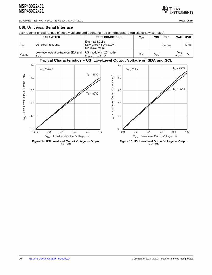
USI, Universal Serial Interfaceover recommended ranges of supply voltage and operating free-air temperature (unless otherwise noted)
PARAMETER TEST CONDITIONS VCC MIN TYP MAX UNIT
External: SCLK;fUSI USI clock frequency Duty cycle = 50% ±10%; fSYSTEM MHz
SPI slave mode
Low-level output voltage on SDA and USI module in I2C mode, VSSVOL,I2C 3 V VSS VSCL I(OLmax) = 1.5 mA + 0.4
Typical Characteristics – USI Low-Level Output Voltage on SDA and SCL
Figure 14. USI Low-Level Output Voltage vs Output Figure 15. USI Low-Level Output Voltage vs OutputCurrent Current
26 Submit Documentation Feedback Copyright © 2010–2011, Texas Instruments Incorporated
MSP430G2x31MSP430G2x21
www.ti.com SLAS694E –FEBRUARY 2010–REVISED JANUARY 2011
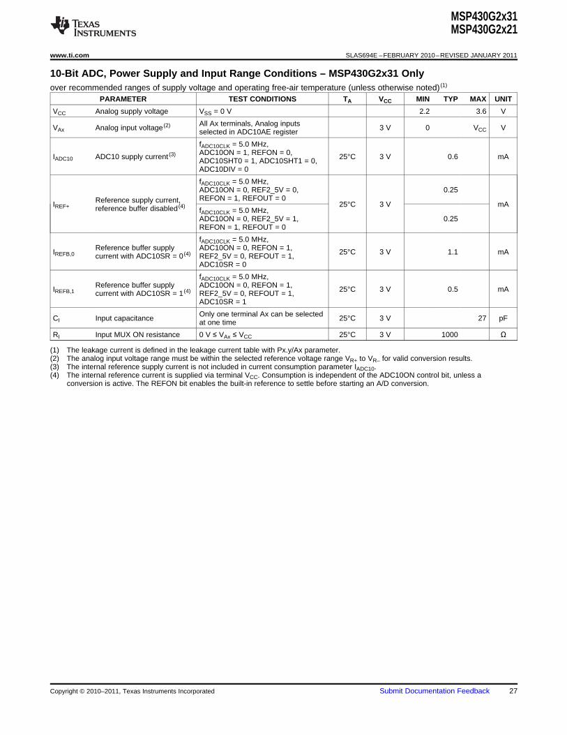
10-Bit ADC, Power Supply and Input Range Conditions – MSP430G2x31 Onlyover recommended ranges of supply voltage and operating free-air temperature (unless otherwise noted) (1)
PARAMETER TEST CONDITIONS TA VCC MIN TYP MAX UNIT
VCC Analog supply voltage VSS = 0 V 2.2 3.6 V
All Ax terminals, Analog inputsVAx Analog input voltage (2) 3 V 0 VCC Vselected in ADC10AE register
fADC10CLK = 5.0 MHz,ADC10ON = 1, REFON = 0,IADC10 ADC10 supply current (3) 25°C 3 V 0.6 mAADC10SHT0 = 1, ADC10SHT1 = 0,ADC10DIV = 0
fADC10CLK = 5.0 MHz,ADC10ON = 0, REF2_5V = 0, 0.25REFON = 1, REFOUT = 0Reference supply current,IREF+ 25°C 3 V mAreference buffer disabled (4)fADC10CLK = 5.0 MHz,ADC10ON = 0, REF2_5V = 1, 0.25REFON = 1, REFOUT = 0
fADC10CLK = 5.0 MHz,Reference buffer supply ADC10ON = 0, REFON = 1,IREFB,0 25°C 3 V 1.1 mAcurrent with ADC10SR = 0 (4) REF2_5V = 0, REFOUT = 1,
ADC10SR = 0
fADC10CLK = 5.0 MHz,Reference buffer supply ADC10ON = 0, REFON = 1,IREFB,1 25°C 3 V 0.5 mAcurrent with ADC10SR = 1 (4) REF2_5V = 0, REFOUT = 1,
ADC10SR = 1
Only one terminal Ax can be selectedCI Input capacitance 25°C 3 V 27 pFat one time
RI Input MUX ON resistance 0 V ≤ VAx ≤ VCC 25°C 3 V 1000 Ω
(1) The leakage current is defined in the leakage current table with Px.y/Ax parameter.(2) The analog input voltage range must be within the selected reference voltage range VR+ to VR– for valid conversion results.(3) The internal reference supply current is not included in current consumption parameter IADC10.(4) The internal reference current is supplied via terminal VCC. Consumption is independent of the ADC10ON control bit, unless a
conversion is active. The REFON bit enables the built-in reference to settle before starting an A/D conversion.
Copyright © 2010–2011, Texas Instruments Incorporated Submit Documentation Feedback 27

MSP430G2x31MSP430G2x21
SLAS694E –FEBRUARY 2010–REVISED JANUARY 2011 www.ti.com
10-Bit ADC, Built-In Voltage Reference – MSP430G2x31 Onlyover recommended ranges of supply voltage and operating free-air temperature (unless otherwise noted)
PARAMETER TEST CONDITIONS VCC MIN TYP MAX UNIT
IVREF+ ≤ 1 mA, REF2_5V = 0 2.2Positive built-in referenceVCC,REF+ Vanalog supply voltage range IVREF+ ≤ 1 mA, REF2_5V = 1 2.9
IVREF+ ≤ IVREF+max, REF2_5V = 0 1.41 1.5 1.59Positive built-in referenceVREF+ 3 V Vvoltage IVREF+ ≤ IVREF+max, REF2_5V = 1 2.35 2.5 2.65
Maximum VREF+ loadILD,VREF+ 3 V ±1 mAcurrent
IVREF+ = 500 µA ± 100 µA,Analog input voltage VAx ≉ 0.75 V, ±2REF2_5V = 0
VREF+ load regulation 3 V LSBIVREF+ = 500 µA ± 100 µA,Analog input voltage VAx ≉ 1.25 V, ±2REF2_5V = 1
IVREF+ = 100 µA→900 µA,VREF+ load regulation VAx ≉ 0.5 × VREF+, 3 V 400 nsresponse time Error of conversion result ≤ 1 LSB,
ADC10SR = 0
Maximum capacitance atCVREF+ IVREF+ ≤ ±1 mA, REFON = 1, REFOUT = 1 3 V 100 pFpin VREF+
ppm/TCREF+ Temperature coefficient IVREF+ = const with 0 mA ≤ IVREF+ ≤ 1 mA 3 V ±100 °C
Settling time of internal IVREF+ = 0.5 mA, REF2_5V = 0,tREFON reference voltage to 99.9% 3.6 V 30 µsREFON = 0 → 1VREF
IVREF+ = 0.5 mA,Settling time of referencetREFBURST REF2_5V = 1, REFON = 1, 3 V 2 µsbuffer to 99.9% VREF REFBURST = 1, ADC10SR = 0
28 Submit Documentation Feedback Copyright © 2010–2011, Texas Instruments Incorporated
MSP430G2x31MSP430G2x21
www.ti.com SLAS694E –FEBRUARY 2010–REVISED JANUARY 2011
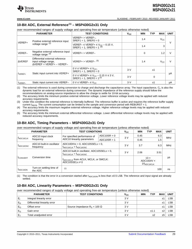
10-Bit ADC, External Reference (1) – MSP430G2x31 Onlyover recommended ranges of supply voltage and operating free-air temperature (unless otherwise noted)
PARAMETER TEST CONDITIONS VCC MIN TYP MAX UNIT
VEREF+ > VEREF–, 1.4 VCCSREF1 = 1, SREF0 = 0Positive external reference inputVEREF+ Vvoltage range (2)VEREF– ≤ VEREF+ ≤ VCC – 0.15 V, 1.4 3SREF1 = 1, SREF0 = 1 (3)
Negative external reference inputVEREF– VEREF+ > VEREF– 0 1.2 Vvoltage range (4)
Differential external referenceΔVEREF input voltage range, VEREF+ > VEREF– (5) 1.4 VCC V
ΔVEREF = VEREF+ – VEREF–
0 V ≤ VEREF+ ≤ VCC, 3 V ±1SREF1 = 1, SREF0 = 0IVEREF+ Static input current into VEREF+ µA
0 V ≤ VEREF+ ≤ VCC – 0.15 V ≤ 3 V, 3 V 0SREF1 = 1, SREF0 = 1 (3)
IVEREF– Static input current into VEREF– 0 V ≤ VEREF– ≤ VCC 3 V ±1 µA
(1) The external reference is used during conversion to charge and discharge the capacitance array. The input capacitance, CI, is also thedynamic load for an external reference during conversion. The dynamic impedance of the reference supply should follow therecommendations on analog-source impedance to allow the charge to settle for 10-bit accuracy.
(2) The accuracy limits the minimum positive external reference voltage. Lower reference voltage levels may be applied with reducedaccuracy requirements.
(3) Under this condition the external reference is internally buffered. The reference buffer is active and requires the reference buffer supplycurrent IREFB. The current consumption can be limited to the sample and conversion period with REBURST = 1.
(4) The accuracy limits the maximum negative external reference voltage. Higher reference voltage levels may be applied with reducedaccuracy requirements.
(5) The accuracy limits the minimum external differential reference voltage. Lower differential reference voltage levels may be applied withreduced accuracy requirements.
10-Bit ADC, Timing Parameters – MSP430G2x31 Onlyover recommended ranges of supply voltage and operating free-air temperature (unless otherwise noted)
PARAMETER TEST CONDITIONS VCC MIN TYP MAX UNIT
ADC10SR = 0 0.45 6.3ADC10 input clock For specified performance offADC10CLK 3 V MHzfrequency ADC10 linearity parameters ADC10SR = 1 0.45 1.5
ADC10 built-in oscillator ADC10DIVx = 0, ADC10SSELx = 0,fADC10OSC 3 V 3.7 6.3 MHzfrequency fADC10CLK = fADC10OSC
ADC10 built-in oscillator, ADC10SSELx = 0, 3 V 2.06 3.51fADC10CLK = fADC10OSC
tCONVERT Conversion time µs13 ×fADC10CLK from ACLK, MCLK, or SMCLK: ADC10DIV ×ADC10SSELx ≠ 0 1/fADC10CLK
Turn-on settling time oftADC10ON(1) 100 nsthe ADC
(1) The condition is that the error in a conversion started after tADC10ON is less than ±0.5 LSB. The reference and input signal are alreadysettled.
10-Bit ADC, Linearity Parameters – MSP430G2x31 Onlyover recommended ranges of supply voltage and operating free-air temperature (unless otherwise noted)
PARAMETER TEST CONDITIONS VCC MIN TYP MAX UNIT
EI Integral linearity error 3 V ±1 LSB
ED Differential linearity error 3 V ±1 LSB
EO Offset error Source impedance RS < 100 Ω 3 V ±1 LSB
EG Gain error 3 V ±1.1 ±2 LSB
ET Total unadjusted error 3 V ±2 ±5 LSB
Copyright © 2010–2011, Texas Instruments Incorporated Submit Documentation Feedback 29
MSP430G2x31MSP430G2x21
SLAS694E –FEBRUARY 2010–REVISED JANUARY 2011 www.ti.com
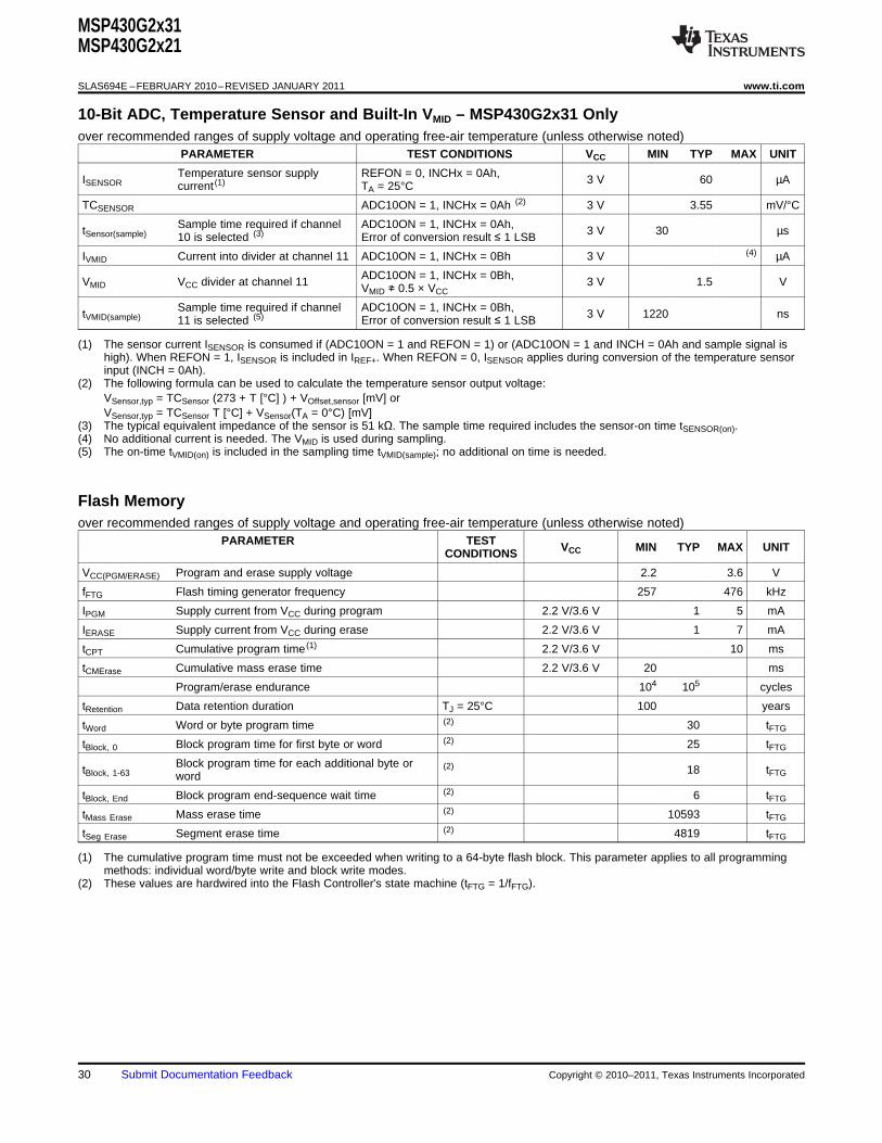
10-Bit ADC, Temperature Sensor and Built-In VMID – MSP430G2x31 Onlyover recommended ranges of supply voltage and operating free-air temperature (unless otherwise noted)
PARAMETER TEST CONDITIONS VCC MIN TYP MAX UNIT
Temperature sensor supply REFON = 0, INCHx = 0Ah,ISENSOR 3 V 60 µAcurrent (1) TA = 25°C
TCSENSOR ADC10ON = 1, INCHx = 0Ah (2) 3 V 3.55 mV/°C
Sample time required if channel ADC10ON = 1, INCHx = 0Ah,tSensor(sample) 3 V 30 µs10 is selected (3) Error of conversion result ≤ 1 LSB
IVMID Current into divider at channel 11 ADC10ON = 1, INCHx = 0Bh 3 V (4) µA
ADC10ON = 1, INCHx = 0Bh,VMID VCC divider at channel 11 3 V 1.5 VVMID ≉ 0.5 × VCC
Sample time required if channel ADC10ON = 1, INCHx = 0Bh,tVMID(sample) 3 V 1220 ns11 is selected (5) Error of conversion result ≤ 1 LSB
(1) The sensor current ISENSOR is consumed if (ADC10ON = 1 and REFON = 1) or (ADC10ON = 1 and INCH = 0Ah and sample signal ishigh). When REFON = 1, ISENSOR is included in IREF+. When REFON = 0, ISENSOR applies during conversion of the temperature sensorinput (INCH = 0Ah).
(2) The following formula can be used to calculate the temperature sensor output voltage:VSensor,typ = TCSensor (273 + T [°C] ) + VOffset,sensor [mV] orVSensor,typ = TCSensor T [°C] + VSensor(TA = 0°C) [mV]
(3) The typical equivalent impedance of the sensor is 51 kΩ. The sample time required includes the sensor-on time tSENSOR(on).(4) No additional current is needed. The VMID is used during sampling.(5) The on-time tVMID(on) is included in the sampling time tVMID(sample); no additional on time is needed.
Flash Memoryover recommended ranges of supply voltage and operating free-air temperature (unless otherwise noted)
PARAMETER TEST VCC MIN TYP MAX UNITCONDITIONS
VCC(PGM/ERASE) Program and erase supply voltage 2.2 3.6 V
fFTG Flash timing generator frequency 257 476 kHz
IPGM Supply current from VCC during program 2.2 V/3.6 V 1 5 mA
IERASE Supply current from VCC during erase 2.2 V/3.6 V 1 7 mA
tCPT Cumulative program time (1) 2.2 V/3.6 V 10 ms
tCMErase Cumulative mass erase time 2.2 V/3.6 V 20 ms
Program/erase endurance 104 105 cycles
tRetention Data retention duration TJ = 25°C 100 years
tWord Word or byte program time (2) 30 tFTG
tBlock, 0 Block program time for first byte or word (2) 25 tFTG
Block program time for each additional byte ortBlock, 1-63(2) 18 tFTGword
tBlock, End Block program end-sequence wait time (2) 6 tFTG
tMass Erase Mass erase time (2) 10593 tFTG
tSeg Erase Segment erase time (2) 4819 tFTG
(1) The cumulative program time must not be exceeded when writing to a 64-byte flash block. This parameter applies to all programmingmethods: individual word/byte write and block write modes.
(2) These values are hardwired into the Flash Controller's state machine (tFTG = 1/fFTG).
30 Submit Documentation Feedback Copyright © 2010–2011, Texas Instruments Incorporated
MSP430G2x31MSP430G2x21
www.ti.com SLAS694E –FEBRUARY 2010–REVISED JANUARY 2011
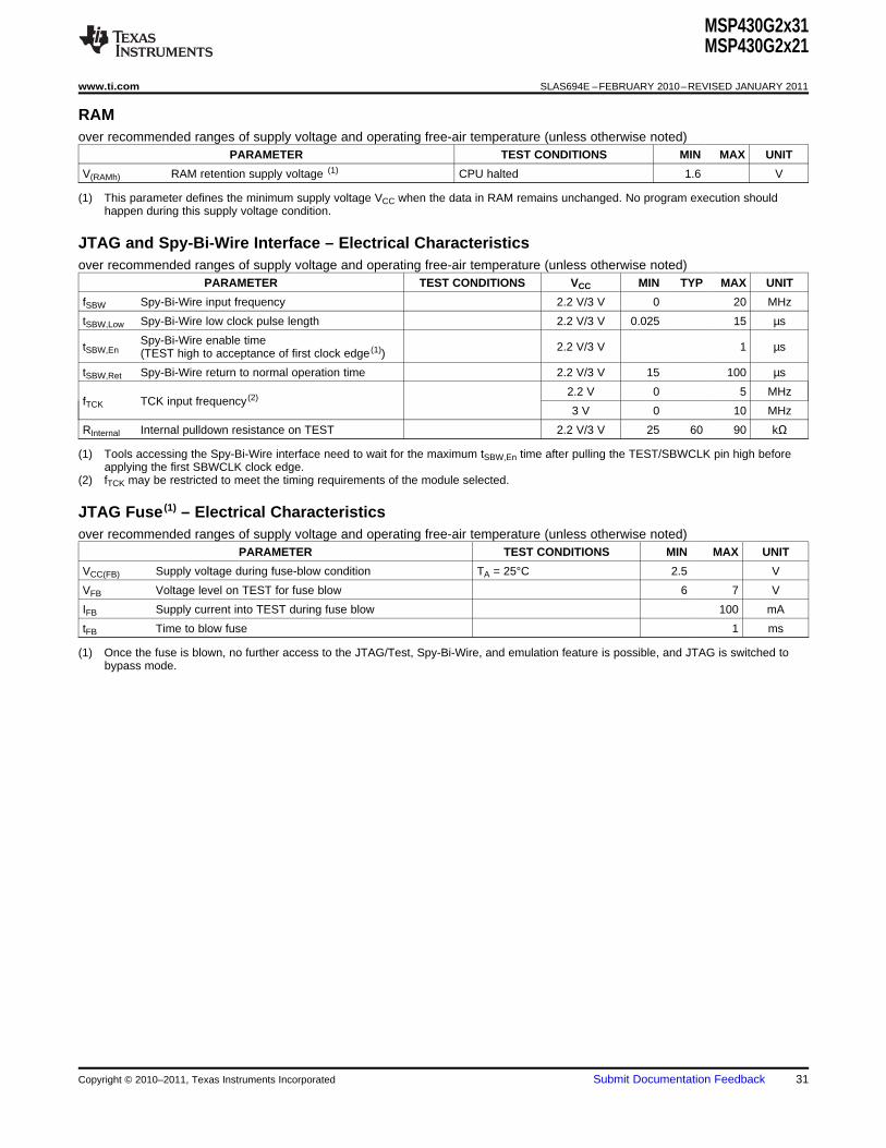
RAMover recommended ranges of supply voltage and operating free-air temperature (unless otherwise noted)
PARAMETER TEST CONDITIONS MIN MAX UNIT
V(RAMh) RAM retention supply voltage (1) CPU halted 1.6 V
(1) This parameter defines the minimum supply voltage VCC when the data in RAM remains unchanged. No program execution shouldhappen during this supply voltage condition.
JTAG and Spy-Bi-Wire Interface – Electrical Characteristicsover recommended ranges of supply voltage and operating free-air temperature (unless otherwise noted)
PARAMETER TEST CONDITIONS VCC MIN TYP MAX UNIT
fSBW Spy-Bi-Wire input frequency 2.2 V/3 V 0 20 MHz
tSBW,Low Spy-Bi-Wire low clock pulse length 2.2 V/3 V 0.025 15 µs
Spy-Bi-Wire enable timetSBW,En 2.2 V/3 V 1 µs(TEST high to acceptance of first clock edge (1))
tSBW,Ret Spy-Bi-Wire return to normal operation time 2.2 V/3 V 15 100 µs
2.2 V 0 5 MHzfTCK TCK input frequency (2)
3 V 0 10 MHz
RInternal Internal pulldown resistance on TEST 2.2 V/3 V 25 60 90 kΩ
(1) Tools accessing the Spy-Bi-Wire interface need to wait for the maximum tSBW,En time after pulling the TEST/SBWCLK pin high beforeapplying the first SBWCLK clock edge.
(2) fTCK may be restricted to meet the timing requirements of the module selected.
JTAG Fuse (1) – Electrical Characteristicsover recommended ranges of supply voltage and operating free-air temperature (unless otherwise noted)
PARAMETER TEST CONDITIONS MIN MAX UNIT
VCC(FB) Supply voltage during fuse-blow condition TA = 25°C 2.5 V
VFB Voltage level on TEST for fuse blow 6 7 V
IFB Supply current into TEST during fuse blow 100 mA
tFB Time to blow fuse 1 ms
(1) Once the fuse is blown, no further access to the JTAG/Test, Spy-Bi-Wire, and emulation feature is possible, and JTAG is switched tobypass mode.
Copyright © 2010–2011, Texas Instruments Incorporated Submit Documentation Feedback 31
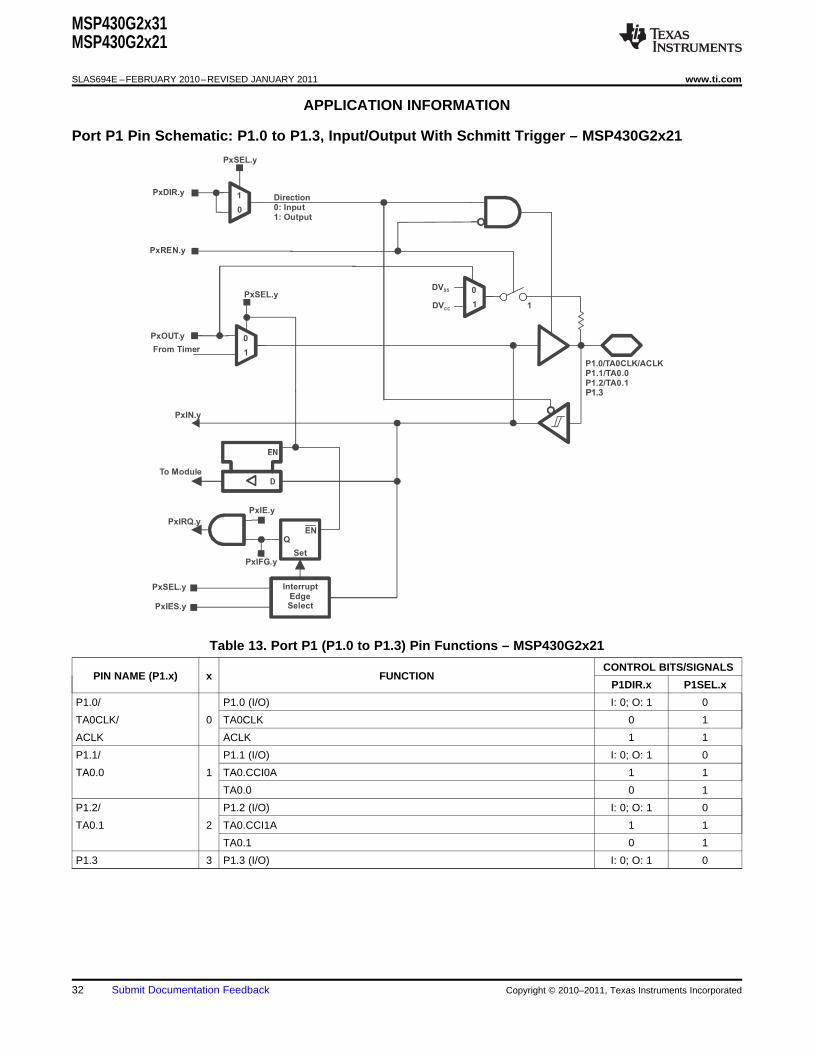
P1.0/TA0CLK/ACLKP1.1/TA0.0P1.2/TA0.1P1.3
To Module
From Timer
PxOUT.y
DVSS
DVCC
1
1
0
PxIN.y
PxSEL.y
PxREN.y
1
0
PxIRQ.y
PxIE.y
EN
Set
Q
InterruptEdgeSelect
PxSEL.y
PxIES.y
PxIFG.y
Direction0: Input1: Output
PxDIR.y
PxSEL.y
0
1
MSP430G2x31MSP430G2x21
SLAS694E –FEBRUARY 2010–REVISED JANUARY 2011 www.ti.com
APPLICATION INFORMATION
Port P1 Pin Schematic: P1.0 to P1.3, Input/Output With Schmitt Trigger – MSP430G2x21
Table 13. Port P1 (P1.0 to P1.3) Pin Functions – MSP430G2x21
CONTROL BITS/SIGNALSPIN NAME (P1.x) x FUNCTION
P1DIR.x P1SEL.x
P1.0/ P1.0 (I/O) I: 0; O: 1 0
TA0CLK/ 0 TA0CLK 0 1
ACLK ACLK 1 1
P1.1/ P1.1 (I/O) I: 0; O: 1 0
TA0.0 1 TA0.CCI0A 1 1
TA0.0 0 1
P1.2/ P1.2 (I/O) I: 0; O: 1 0
TA0.1 2 TA0.CCI1A 1 1
TA0.1 0 1
P1.3 3 P1.3 (I/O) I: 0; O: 1 0
32 Submit Documentation Feedback Copyright © 2010–2011, Texas Instruments Incorporated

To Module
From Module
PxOUT.y
DVSS
DVCC 1
1
0
PxIN.y
PxSEL.y
PxREN.y
1
0
PxIRQ.y
PxIE.y
EN
Set
Q
InterruptEdgeSelect
PxSEL.y
PxIES.y
PxIFG.y
Direction0: Input1: Output
PxDIR.y
PxSEL.y
0
1
From JTAG
To JTAG
P1.4/SMCLK/TCK
MSP430G2x31MSP430G2x21
www.ti.com SLAS694E –FEBRUARY 2010–REVISED JANUARY 2011
Port P1 Pin Schematic: P1.4, Input/Output With Schmitt Trigger – MSP430G2x21
Table 14. Port P1 (P1.4) Pin Functions – MSP430G2x21
CONTROL BITS / SIGNALS (1)
PIN NAME (P1.x) x FUNCTIONP1DIR.x P1SEL.x JTAG Mode
P1.4/ P1.x (I/O) I: 0; O: 1 0 0
SMCLK/ 4 SMCLK 1 1 0
TCK TCK X X 1
(1) X = don't care
Copyright © 2010–2011, Texas Instruments Incorporated Submit Documentation Feedback 33

To Module
From USI
PxOUT.y
DVSS
DVCC 1
1
0
PxIN.y
PxREN.y
1
0
PxIRQ.y
PxIE.y
EN
Set
Q
InterruptEdge
Select
PxSEL.y
PxIES.y
PxIFG.y
Direction0: Input1: Output
PxDIR.y
PxSEL.y
0
1
From JTAG
To JTAG
P1.5/TA0.0/SCLK/TMS
PxSEL.y orUSIPE5
PxSEL.y
From USI
MSP430G2x31MSP430G2x21
SLAS694E –FEBRUARY 2010–REVISED JANUARY 2011 www.ti.com
Port P1 Pin Schematic: P1.5, Input/Output With Schmitt Trigger – MSP430G2x21
Table 15. Port P1 (P1.5) Pin Functions – MSP430G2x21
CONTROL BITS / SIGNALS (1)
PIN NAME (P1.x) x FUNCTIONP1DIR.x P1SEL.x USIP.x JTAG Mode
P1.5/ P1.x (I/O) I: 0; O: 1 0 0 0
TA0.0/ TA0.0 1 1 0 05
SCLK/ SCLK X X 1 0
TMS TMS X X 0 1
(1) X = don't care
34 Submit Documentation Feedback Copyright © 2010–2011, Texas Instruments Incorporated

To Module
From Module
PxOUT.y
DVSS
DVCC 1
1
0
PxIN.y
PxREN.y
1
0
PxIRQ.y
PxIE.y
EN
Set
Q
InterruptEdgeSelect
PxSEL.y
PxIES.y
PxIFG.y
Direction0: Input1: Output
PxDIR.y
PxSEL.y
0
1
From JTAG
To JTAG
P1.6/TA0.1/SDO/SCL/TDI
PxSEL.y orUSIPE6
PxSEL.y
MSP430G2x31MSP430G2x21
www.ti.com SLAS694E –FEBRUARY 2010–REVISED JANUARY 2011
Port P1 Pin Schematic: P1.6, Input/Output With Schmitt Trigger – MSP430G2x21
Table 16. Port P1 (P1.6) Pin Functions – MSP430G2x21
CONTROL BITS / SIGNALS (1)
PIN NAME (P1.x) x FUNCTIONP1DIR.x P1SEL.x USIP.x JTAG Mode
P1.6/ P1.x (I/O) I: 0; O: 1 0 0 0
TA0.1/ TA0.1 1 1 0 0
6 TA0.CCI1B 0 1 0 0
SDO/SCL/ SDO/SCL X X 1 0
TDI/TCLK TDI/TCLK X X 0 1
(1) X = don't care
Copyright © 2010–2011, Texas Instruments Incorporated Submit Documentation Feedback 35

To Module
From USI
PxOUT.y
DVSS
DVCC
1
1
0
PxIN.y
PxREN.y
1
0
PxIRQ.y
PxIE.y
EN
Set
Q
InterruptEdgeSelect
PxSEL.y
PxIES.y
PxIFG.y
Direction0: Input1: Output
PxDIR.y
USIPE7
0
1
From JTAG
To JTAG
P1.7/SDI/SDA/TDO/TDI
PxSEL.y orUSIPE7
PxSEL.y
From JTAG
To JTAG
From USI
MSP430G2x31MSP430G2x21
SLAS694E –FEBRUARY 2010–REVISED JANUARY 2011 www.ti.com
Port P1 Pin Schematic: P1.7, Input/Output With Schmitt Trigger – MSP430G2x21
Table 17. Port P1 (P1.7) Pin Functions – MSP430G2x21
CONTROL BITS / SIGNALS (1)
PIN NAME (P(1.x) x FUNCTIONP1DIR.x P1SEL.x USIP.x JTAG Mode
P1.7/ P1.x (I/O) I: 0; O: 1 0 0 0
SDI/SDA/ 7 SDI/SDA X X 1 0
TDO/TDI TDO/TDI X X 0 1
(1) X = don't care
36 Submit Documentation Feedback Copyright © 2010–2011, Texas Instruments Incorporated
P1.0/TA0CLK/ACLK/A0P1.1/TA0.0/A1P1.2/TA0.1/A2
To Module
ACLK
PxOUT.y
DVSS
DVCC 1
BusKeeper
EN
1
0
PxIN.y
PxSEL.y
PxREN.y
1
0
INCHx
To ADC10
PxIRQ.y
PxIE.y
EN
Set
Q
InterruptEdgeSelect
PxSEL.y
PxIES.y
PxIFG.y
Direction0: Input1: Output
PxDIR.y
PxSEL.y
0
1
ADC10AE0.y
MSP430G2x31MSP430G2x21
www.ti.com SLAS694E –FEBRUARY 2010–REVISED JANUARY 2011
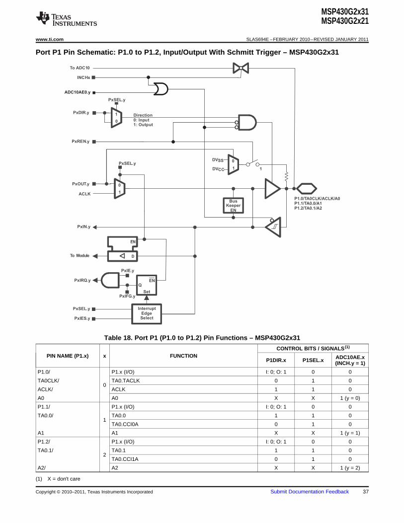
Port P1 Pin Schematic: P1.0 to P1.2, Input/Output With Schmitt Trigger – MSP430G2x31
Table 18. Port P1 (P1.0 to P1.2) Pin Functions – MSP430G2x31
CONTROL BITS / SIGNALS (1)
PIN NAME (P1.x) x FUNCTION ADC10AE.xP1DIR.x P1SEL.x (INCH.y = 1)
P1.0/ P1.x (I/O) I: 0; O: 1 0 0
TA0CLK/ TA0.TACLK 0 1 00
ACLK/ ACLK 1 1 0
A0 A0 X X 1 (y = 0)
P1.1/ P1.x (I/O) I: 0; O: 1 0 0
TA0.0/ TA0.0 1 1 01
TA0.CCI0A 0 1 0
A1 A1 X X 1 (y = 1)
P1.2/ P1.x (I/O) I: 0; O: 1 0 0
TA0.1/ TA0.1 1 1 02
TA0.CCI1A 0 1 0
A2/ A2 X X 1 (y = 2)
(1) X = don't care
Copyright © 2010–2011, Texas Instruments Incorporated Submit Documentation Feedback 37

To Module
ADC10CLK
PxOUT.y
DVSS
DVCC 1
BusKeeper
EN
1
0
PxIN.y
EN
D
PxSEL.y
PxREN.y
1
0
PxIRQ.y
PxIE.y
EN
Set
Q
InterruptEdgeSelect
PxSEL.y
PxIES.y
PxIFG.y
Direction0: Input1: Output
PxDIR.y
PxSEL.y
0
1
P1.3/ADC10CLK/A3/VREF-/VEREF-
INCHx = y
To ADC10
To ADC10 VREF-1
0 VSS
SREF2
ADC10AE0.y
MSP430G2x31MSP430G2x21
SLAS694E –FEBRUARY 2010–REVISED JANUARY 2011 www.ti.com
Port P1 Pin Schematic: P1.3, Input/Output With Schmitt Trigger – MSP430G2x31
Table 19. Port P1 (P1.3) Pin Functions – MSP430G2x31
CONTROL BITS / SIGNALS (1)
PIN NAME (P1.x) x FUNCTION ADC10AE.xP1DIR.x P1SEL.x (INCH.x = 1)
P1.3/ P1.x (I/O) I: 0; O: 1 0 0
ADC10CLK/ ADC10CLK 1 1 0
A3/ 3 A3 X X 1 (y = 3)
VREF-/ VREF- X X 1
VEREF- VEREF- X X 1
(1) X = don't care
38 Submit Documentation Feedback Copyright © 2010–2011, Texas Instruments Incorporated

To Module
SMCLK
PxOUT.y
DVSS
DVCC 1
BusKeeper
EN
1
0
PxIN.y
PxSEL.y
PxREN.y
1
0
PxIRQ.y
PxIE.y
EN
Set
Q
InterruptEdgeSelect
PxSEL.y
PxIES.y
PxIFG.y
Direction0: Input1: Output
PxDIR.y
PxSEL.y
0
1
P1.4/SMCLK/A4/VREF+/VEREF+/TCK
INCHx = y
To ADC10
To ADC10 VREF+
ADC10AE0.y
From JTAG
To JTAG
MSP430G2x31MSP430G2x21
www.ti.com SLAS694E –FEBRUARY 2010–REVISED JANUARY 2011
Port P1 Pin Schematic: P1.4, Input/Output With Schmitt Trigger – MSP430G2x31
Table 20. Port P1 (P1.4) Pin Functions – MSP430G2x31
CONTROL BITS / SIGNALS (1)
PIN NAME (P1.x) x FUNCTION ADC10AE.x JTAGP1DIR.x P1SEL.x (INCH.x = 1) Mode
P1.4/ P1.x (I/O) I: 0; O: 1 0 0 0
SMCLK/ SMCLK 1 1 0 0
A4/ A4 X X 1 (y = 4) 04
VREF+/ VREF+ X X 1 0
VEREF+/ VEREF+ X X 1 0
TCK TCK X X 0 1
(1) X = don't care
Copyright © 2010–2011, Texas Instruments Incorporated Submit Documentation Feedback 39

BusKeeper
EN
P1.5/TA0.0/A5/TMS
To Module
From Module
PxOUT.y
DVSS
DVCC
1
1
0
PxIN.y
PxSEL.y
PxREN.y
1
0
PxIRQ.y
PxIE.y
EN
Set
Q
InterruptEdgeSelect
PxSEL.y
PxIES.y
PxIFG.y
Direction0: Input1: Output
PxDIR.y
PxSEL.y
0
1
From JTAG
To JTAG
INCHx
To ADC10
ADC10AE0.y
MSP430G2x31MSP430G2x21
SLAS694E –FEBRUARY 2010–REVISED JANUARY 2011 www.ti.com
Port P1 Pin Schematic: P1.5, Input/Output With Schmitt Trigger – MSP430G2x31
Table 21. Port P1 (P1.5) Pin Functions - MSP430G2x31
CONTROL BITS / SIGNALS (1)
PIN NAME (P1.x) x FUNCTION ADC10AE.x JTAGP1DIR.x P1SEL.x USIP.x (INCH.x = 1) Mode
P1.5/ P1.x (I/O) I: 0; O: 1 0 0 0 0
TA0.0/ TA0.0 1 1 0 0 0
A5/ 5 A5 X X X 1 (y = 5) 0
SCLK/ SCLK X X 1 0 0
TMS TMS X X 0 0 1
(1) X = don't care
40 Submit Documentation Feedback Copyright © 2010–2011, Texas Instruments Incorporated

BusKeeper
EN
P1.6/TA0.1/SDO/SCL/A6/TDI
To Module
From USI
PxOUT.y
DVSS
DVCC
1
1
0
PxIN.y
PxSEL.y orUSIPE6
PxREN.y
1
0
PxIRQ.y
PxIE.y
EN
Set
Q
InterruptEdgeSelect
PxSEL.y
PxIES.y
PxIFG.y
Direction0: Input1: Output
PxDIR.y
USIPE6
0
1
From JTAG
To JTAG
INCHx
To ADC10
ADC10AE0.y
from USI
PxSEL.y
USI in I2C mode: Output driver drives low level only. Driver is disabled in JTAG mode.
MSP430G2x31MSP430G2x21
www.ti.com SLAS694E –FEBRUARY 2010–REVISED JANUARY 2011
Port P1 Pin Schematic: P1.6, Input/Output With Schmitt Trigger – MSP430G2x31
Table 22. Port P1 (P1.6) Pin Functions - MSP430G2x31
CONTROL BITS / SIGNALS (1)
PIN NAME (P1.x) x FUNCTION ADC10AE.x JTAGP1DIR.x P1SEL.x USIP.x (INCH.x = 1) Mode
P1.6/ P1.x (I/O) I: 0; O: 1 0 0 0 0
TA0.1/ TA0.1 1 1 0 0 0
TA0.CCR1B 0 1 0 0 06
A6/ A6 X X 0 1 (y = 6) 0
SDO/ SDO X X 1 0 0
TDI/TCLK TDI/TCLK X X 0 0 1
(1) X = don't care
Copyright © 2010–2011, Texas Instruments Incorporated Submit Documentation Feedback 41

BusKeeper
EN
P1.7/SDI/SDA/A7/TDO/TDI
To Module
From USI
PxOUT.y
DVSS
DVCC 1
1
0
PxIN.y
PxREN.y
1
0
PxIRQ.y
PxIE.y
EN
Set
Q
InterruptEdgeSelect
PxSEL.y
PxIES.y
PxIFG.y
Direction0: Input1: Output
PxDIR.y
USIPE7
0
1
From JTAG
To JTAG
INCHx
To ADC10
ADC10AE0.y
from USI
PxSEL.y
PxSEL.y orUSIPE7
PxSEL.y
From JTAG
To JTAG
USI in I2C mode: Output driver drives low level only. Driver is disabled in JTAG mode.
MSP430G2x31MSP430G2x21
SLAS694E –FEBRUARY 2010–REVISED JANUARY 2011 www.ti.com
Port P1 Pin Schematic: P1.7, Input/Output With Schmitt Trigger – MSP430G2x31
Table 23. Port P1 (P1.7) Pin Functions – MSP430G2x31
CONTROL BITS / SIGNALS (1)
PIN NAME (P1.x) x FUNCTION ADC10AE.x JTAGP1DIR.x P1SEL.x USIP.x (INCH.x = 1) Mode
P1.7/ P1.x (I/O) I: 0; O: 1 0 0 0 0
A7/ A7 X X 0 1 (y = 7) 07
SDI/SDO SDI/SDO X X 1 0 0
TDO/TDI TDO/TDI X X 0 0 1
(1) X = don't care
42 Submit Documentation Feedback Copyright © 2010–2011, Texas Instruments Incorporated
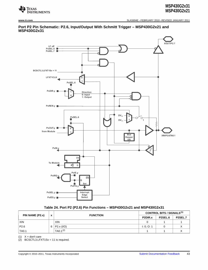
XIN/P2.6/TA0.1
1
0
XOUT/P2.7
LF off
LFXT1CLK
PxSEL.6PxSEL.7
BCSCTL3.LFXT1Sx = 11
To Module
from Module
PxOUT.y
DVSS
DVCC 1
BusKeeper
EN
1
0
PxIN.y
PxSEL.6
PxREN.y
1
0
PxIRQ.y
PxIE.y
EN
Set
Q
InterruptEdge
Select
PxSEL.y
PxIES.y
PxIFG.y
Direction0: Input1: Output
PxDIR.y
PxSEL.6
0
1
MSP430G2x31MSP430G2x21
www.ti.com SLAS694E –FEBRUARY 2010–REVISED JANUARY 2011
Port P2 Pin Schematic: P2.6, Input/Output With Schmitt Trigger – MSP430G2x21 andMSP430G2x31
Table 24. Port P2 (P2.6) Pin Functions – MSP430G2x21 and MSP430G2x31
CONTROL BITS / SIGNALS (1)
PIN NAME (P2.x) x FUNCTIONP2DIR.x P2SEL.6 P2SEL.7
XIN XIN 0 1 1
P2.6 6 P2.x (I/O) I: 0; O: 1 0 X
TA0.1 TA0.1 (2) 1 1 X
(1) X = don't care(2) BCSCTL3.LFXT1Sx = 11 is required.
Copyright © 2010–2011, Texas Instruments Incorporated Submit Documentation Feedback 43

XIN/P2.6/TA0.1
1
0
XOUT/P2.7
LF off
LFXT1CLK
PxSEL.6PxSEL.7
BCSCTL3.LFXT1Sx = 11
To Module
from Module
PxOUT.y
DVSS
DVCC 1
BusKeeper
EN
1
0
PxIN.y
PxSEL.7
PxREN.y
1
0
PxIRQ.y
PxIE.y
EN
Set
Q
InterruptEdgeSelect
PxSEL.y
PxIES.y
PxIFG.y
Direction0: Input1: Output
PxDIR.y
PxSEL.7
0
1
from P2.6/XIN
MSP430G2x31MSP430G2x21
SLAS694E –FEBRUARY 2010–REVISED JANUARY 2011 www.ti.com
Port P2 Pin Schematic: P2.7, Input/Output With Schmitt Trigger – MSP430G2x21 andMSP430G2x31
Table 25. Port P2 (P2.7) Pin Functions – MSP430G2x21 and MSP430G2x31
CONTROL BITS / SIGNALS (1)
PIN NAME (P2.x) x FUNCTIONP2DIR.x P2SEL.6 P2SEL.7
XOUT XOUT 1 1 17
P2.7 P2.x (I/O) I: 0; O: 1 0 X
(1) X = don't care
44 Submit Documentation Feedback Copyright © 2010–2011, Texas Instruments Incorporated


![HMO3004 - farnell.com · HMO3004 Serie 4-Kanal Mixed-Signal-Oszilloskope HMO3002 Serie 2-Kanal Mixed-Signal-Oszilloskope HMO3032 [HMO3034] 300 MHz](https://static.fdocument.pub/doc/165x107/5e0fe9d4d38f1d4fce090348/hmo3004-hmo3004-serie-4-kanal-mixed-signal-oszilloskope-hmo3002-serie-2-kanal.jpg)


