LXDC55FAAA-203 - 秋月電子通商akizukidenshi.com/download/ds/murata/LXDC55FAAA-203.pdf ·...
23
LXDC55FAAA-203 Micro DC-DC converter 1 Dec 2014 1. Features Wide Input voltage range : 4.0V to 14.0V User Adjustable Output voltage : 0.8 to 5.3V Small footprint Buck converter for up to 1.5A output current application Low EMI noise by using an inductor-embedded ferrite substrate High efficiency using synchronous rectifier technology at 2MHz operation Superior transient response using quasi-fixed-frequency COT technology Seamless Power-Save Mode Transition Power-Good function ,Over current protection, Over temperature protection Quiescent Current of 150 μA (typ.) 2. Description The LXDC55F series is an easy-to-use synchronous step-down DC-DC converter optimized for applications with high power density. The device utilizes an inductor-embedded ferrite substrate, and the substrate eliminates radiated EMI noise and conduction noise efficiently. With its wide operating input voltage range of 4 V to 14 V, the devices are ideally suited for systems powered from either a Li-Ion or other batteries, as well as from 12-V intermediate power rails. It supports up to 1.5 A of continuous output current at output voltages between 0.8 V and 5.3 V The LXDC55F series utilizes a constant on time feedback technology and has superior load transient response. It has a unique circuit that roughly keeps the switching frequency constant, which makes it easy to filter the switching noise. The output voltage of LXDC55F series can be adjusted from 0.8 V to 5.3 V by using a resistor (RFB) between FB pin and GND pin. In terms of resistor value is calculated by RFB = 7.28/(Vout-0.8V) – 1.6 [kohm] The LXDC55F series has Power Good Output function. It’s to indicate whether the output voltage has reached its appropriate level or not. The device has an internal soft-start function to control the output voltage slope during start-up. In power-save mode, the devices show quiescent current of about 150 μA from VIN. Power-save mod e, it enters automatically and seamlessly if load is small, maintains high efficiency over the entire load range. 3. Typical Application Circuit
-
Upload
phungtuong -
Category
Documents
-
view
214 -
download
0
Transcript of LXDC55FAAA-203 - 秋月電子通商akizukidenshi.com/download/ds/murata/LXDC55FAAA-203.pdf ·...

LXDC55FAAA-203 Micro DC-DC converter
1
Dec 2014
1. Features Wide Input voltage range : 4.0V to 14.0V User Adjustable Output voltage : 0.8 to 5.3V Small footprint Buck converter for up to 1.5A output current application Low EMI noise by using an inductor-embedded ferrite substrate High efficiency using synchronous rectifier technology at 2MHz operation Superior transient response using quasi-fixed-frequency COT technology Seamless Power-Save Mode Transition Power-Good function ,Over current protection, Over temperature protection Quiescent Current of 150 μA (typ.) 2. Description The LXDC55F series is an easy-to-use synchronous step-down DC-DC converter optimized for applications with high power density. The device utilizes an inductor-embedded ferrite substrate, and the substrate eliminates radiated EMI noise and conduction noise efficiently. With its wide operating input voltage range of 4 V to 14 V, the devices are ideally suited for systems powered from either a Li-Ion or other batteries, as well as from 12-V intermediate power rails. It supports up to 1.5 A of continuous output current at output voltages between 0.8 V and 5.3 V The LXDC55F series utilizes a constant on time feedback technology and has superior load transient response. It has a unique circuit that roughly keeps the switching frequency constant, which makes it easy to filter the switching noise. The output voltage of LXDC55F series can be adjusted from 0.8 V to 5.3 V by using a resistor (RFB) between FB pin and GND pin. In terms of resistor value is calculated by RFB = 7.28/(Vout-0.8V) – 1.6 [kohm] The LXDC55F series has Power Good Output function. It’s to indicate whether the output voltage has reached its appropriate level or not. The device has an internal soft-start function to control the output voltage slope during start-up. In power-save mode, the devices show quiescent current of about 150 μA from VIN. Power-save mod e, it enters automatically and seamlessly if load is small, maintains high efficiency over the entire load range. 3. Typical Application Circuit

LXDC55FAAA-203 Micro DC-DC converter
2
Dec 2014
4. Mechanical details 4-1 Outline
Unit:(mm)
Mark Dimension Mark Dimension
L 5.0 +/- 0.2 e 1.1
W 5.7 +/- 0.2 f 0.6
T 2.1 MAX g 0.35
a 0.25 h 0.6
b 0.7 i 0.35
c 0.4 j 1.0
d 0.8
4-2. Pin Function
Pin No. Symbol I/O Description
1 EN Input
This is the ON/OFF control pin of the device. The device is in shutdown when the voltage to this pin is below 0.3V. Pulling this pin above 0.9V enables the device with soft start. This pin should not be left floating. EN=H: Device ON, EN=L: Device OFF
2 NC - No connection
3,4,5 Vin Input Vin pin supplies current to the LXDC55F internal regulator.
6,12,13,14 GND - Ground pin
7,8,9 Vout Output Regulated voltage output pin. Apply output load between this pin and GND.
10 PG Output Power good voltage output pin (Open drain). This is to indicate
whether the output voltage has reached its appropriate level or not.
11 FB Input External resistor connection pin for output voltage setting

LXDC55FAAA-203 Micro DC-DC converter
3
Dec 2014
4-3. Functional Block Diagram
5. Ordering Information
Part number Device Specific Feature MOQ
LXDC55FAAA-203 Standard Type T/R, 1,000pcs/R
6. Electrical Specification
6-1 Absolute maximum ratings
Parameter symbol rating Unit
Input voltage Vin 16 V
Enable voltage EN Vin V
Operating Ambient temperature Ta -40 to +85 oC
Operating IC temperature TIC -40 to +125 oC
Storage temperature TSTO -40 to +85 oC
LXDC55FAAA-203 Micro DC-DC converter
4
Dec 2014
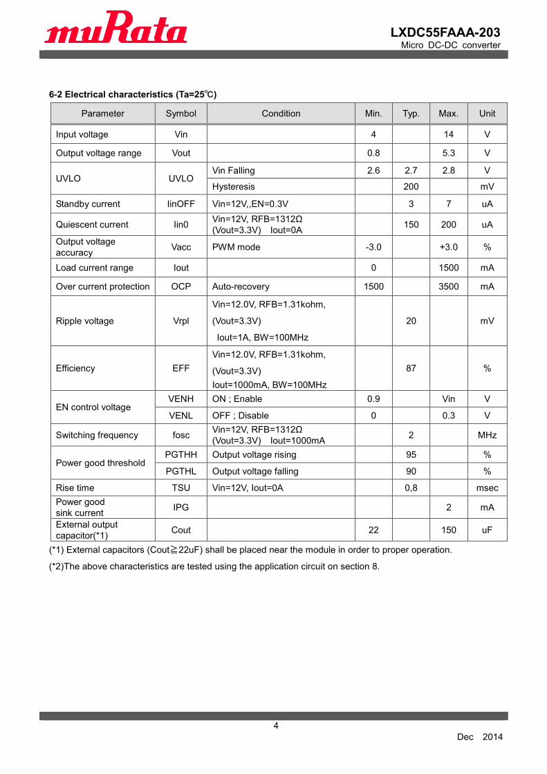
6-2 Electrical characteristics (Ta=25℃)
Parameter Symbol Condition Min. Typ. Max. Unit
Input voltage Vin 4 14 V
Output voltage range Vout 0.8 5.3 V
UVLO UVLO Vin Falling 2.6 2.7 2.8 V
Hysteresis 200 mV
Standby current IinOFF Vin=12V,,EN=0.3V 3 7 uA
Quiescent current Iin0 Vin=12V, RFB=1312Ω (Vout=3.3V) Iout=0A 150 200 uA
Output voltage accuracy Vacc PWM mode -3.0 +3.0 %
Load current range Iout 0 1500 mA
Over current protection OCP Auto-recovery 1500 3500 mA
Ripple voltage Vrpl
Vin=12.0V, RFB=1.31kohm,
(Vout=3.3V)
Iout=1A, BW=100MHz
20 mV
Efficiency EFF Vin=12.0V, RFB=1.31kohm,
(Vout=3.3V) Iout=1000mA, BW=100MHz
87 %
EN control voltage VENH ON ; Enable 0.9 Vin V
VENL OFF ; Disable 0 0.3 V
Switching frequency fosc Vin=12V, RFB=1312Ω (Vout=3.3V) Iout=1000mA 2 MHz
Power good threshold PGTHH Output voltage rising 95 %
PGTHL Output voltage falling 90 %
Rise time TSU Vin=12V, Iout=0A 0,8 msec Power good sink current IPG 2 mA
External output capacitor(*1) Cout 22 150 uF
(*1) External capacitors (Cout≧22uF) shall be placed near the module in order to proper operation.
(*2)The above characteristics are tested using the application circuit on section 8.
LXDC55FAAA-203 Micro DC-DC converter
5
Dec 2014
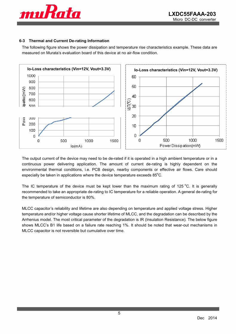
6-3 Thermal and Current De-rating Information The following figure shows the power dissipation and temperature rise characteristics example. These data are measured on Murata’s evaluation board of this device at no air-flow condition. The output current of the device may need to be de-rated if it is operated in a high ambient temperature or in a continuous power delivering application. The amount of current de-rating is highly dependent on the environmental thermal conditions, i.e. PCB design, nearby components or effective air flows. Care should especially be taken in applications where the device temperature exceeds 85oC. The IC temperature of the device must be kept lower than the maximum rating of 125 oC. It is generally recommended to take an appropriate de-rating to IC temperature for a reliable operation. A general de-rating for the temperature of semiconductor is 80%. MLCC capacitor’s reliability and lifetime are also depending on temperature and applied voltage stress. Higher temperature and/or higher voltage cause shorter lifetime of MLCC, and the degradation can be described by the Arrhenius model. The most critical parameter of the degradation is IR (Insulation Resistance). The below figure shows MLCC’s B1 life based on a failure rate reaching 1%. It should be noted that wear-out mechanisms in MLCC capacitor is not reversible but cumulative over time.
Io-Loss characteristics (Vin=12V, Vout=3.3V) Io-Loss characteristics (Vin=12V, Vout=3.3V)

LXDC55FAAA-203 Micro DC-DC converter
6
Dec 2014
The following steps should be taken before the design fix of user’s set for a reliable operation. 1. The ambient temperature of the device should be kept below 85 oC 2. The IC temperature should be measured on the worst condition of each application. The temperature must be
kept below 125 oC. An appropriate de-rating of temperature and/or output current should be taken. 3. The MLCC temperature should be measured on the worst condition of each application. Considering the
above figure, it should be checked if the expected B1 life of MLCC is acceptable or not.
LXDC55FAAA-203 Micro DC-DC converter
7
Dec 2014
7. Detailed Description Adjustable output voltage The output voltage of LXDC55F series can be adjusted from 0.8 V to 5.3 V by using a resistor (RFB) between FB pin and GND pin. In terms of resistor value is calculated by RFB = 7.28/(Vout-0.8V) – 1.6 [kohm]. Pulse-Width Modulation (PWM) Operation The LXDC55F series operates with pulse-width modulation in continuous-conduction mode (CCM). The device operates in PWM mode as long the output current is higher than half the inductor ripple current. To maintain high efficiency at light loads, the device enters power-save mode at the boundary to discontinuous conduction mode (DCM). This happens if the output current becomes smaller than half the inductor ripple current. Power-Save Mode Operation The LXDC55F series enters its built-in power-save mode seamlessly if the load current decreases. This secures a high efficiency in light-load operation. The device remains in power-save mode as long as the inductor current is discontinuous. In power-save mode, the switching frequency decreases linearly with the load current, maintaining high efficiency. The transition into and out of power-save mode happens within the entire regulation scheme and is seamless in both directions. UVLO (Under Voltage Lock Out) The input voltage (Vin) must reach or exceed the UVLO voltage (2.7Vtyp) before the device begins the start up sequence even when the EN pin is kept high. The UVLO function protects against unstable operation at low Vin levels Enable The device starts operation when EN is set high and starts up with soft start. For proper operation, the EN pin must be terminated to logic high and must not left floating. Pulling the EN pin to logic low forces the device shutdown. Power Good (PG) The LXDC55F series has a built-in power-good (PG) function to indicate whether the output voltage has reached its appropriate level or not. It can sink 2mA current and maintain its specified logic-low level. 100% Duty Cycle Operation The duty cycle of the buck converter is given by D = Vout/Vin and increases as the input voltage comes close to the output voltage. In this case, the device starts 100% duty-cycle operation, turning on the high-side switch 100% of the time. The high-side switch stays turned on as long as the output voltage is below the internal set point. This allows the conversion of small input-to-output voltage differences, e.g., for longest operation time of battery-powered applications. In 100% duty-cycle mode, the low-side FET is switched off. Over Current Protection The device integrates a current limit function to protect internal components against heavy load or short circuits.If the OCP event is removed, the output voltage recovers to the nominal value automatically. Thermal Shutdown As soon as the internal IC’s junction temperature exceeds 160 (typ), the device goes into thermal shutdown. ℃
The device continues its operation when the Internal IC’s junction temperature again falls below 140 (typ).℃

LXDC55FAAA-203 Micro DC-DC converter
8
Dec 2014
8. Test Circuit
COUT: GRM21BB30J226 (22uF/6.3V MLCC)
9. Reference Land Pattern
unit (mm)
Mark Dimension
b 0.7
c 0.4
d 0.8
e 1.1
f 0.6
c
(5)
(8)(7) (10)(9)
(6) (12)
(11)
(1)(2)
(14) (13)
(3)(4)
bdbb c c c
ef
e
ef
b
LXDC55FAAA-203 Micro DC-DC converter
9
Dec 2014
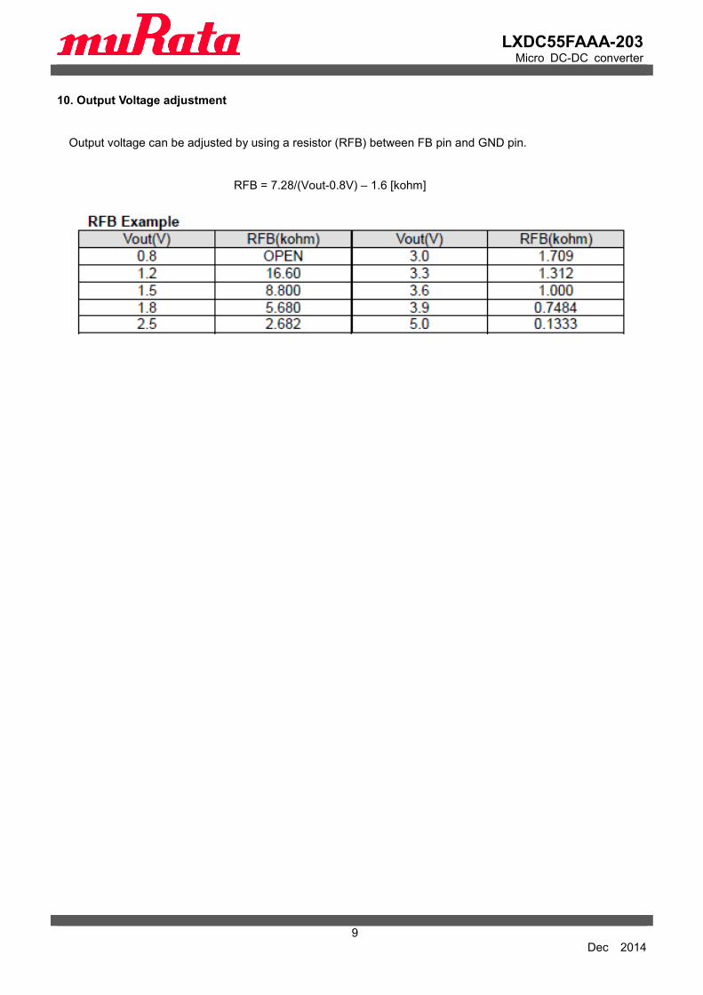
10. Output Voltage adjustment
Output voltage can be adjusted by using a resistor (RFB) between FB pin and GND pin.
RFB = 7.28/(Vout-0.8V) – 1.6 [kohm]

LXDC55FAAA-203 Micro DC-DC converter
10
Dec 2014
Enable SW
Vin
Vin_S GND
Vout_S
Vout
GND_S
GND
GND_S
Power good
11. Measurement Data
Micro DC-DC Converter evaluation board (P2LX1568F)
Measurement setup
* Evaluation board initial output Voltage setting : 3.3V ( resistor : 1.3kΩ + 12Ω )
The enable switch has three positions.
1. When it is toggled to “ON” side, the device starts operation.
2. When it is toggled to “OFF” side, the device stop operation and keep shut down status.
3. When it is set to middle of “ON” and “OFF”, the EN pin becomes floated and can be applied an external
voltage through the EN terminal pin on the EVB. If you don’t apply external voltage to EN pin, the enable
switch should not to be set to the middle position.
A
V
Load
V A
V EN ON
EN OFF
Output voltage adjustment resistor
LXDC55FAAA-203 Micro DC-DC converter
11
Dec 2014
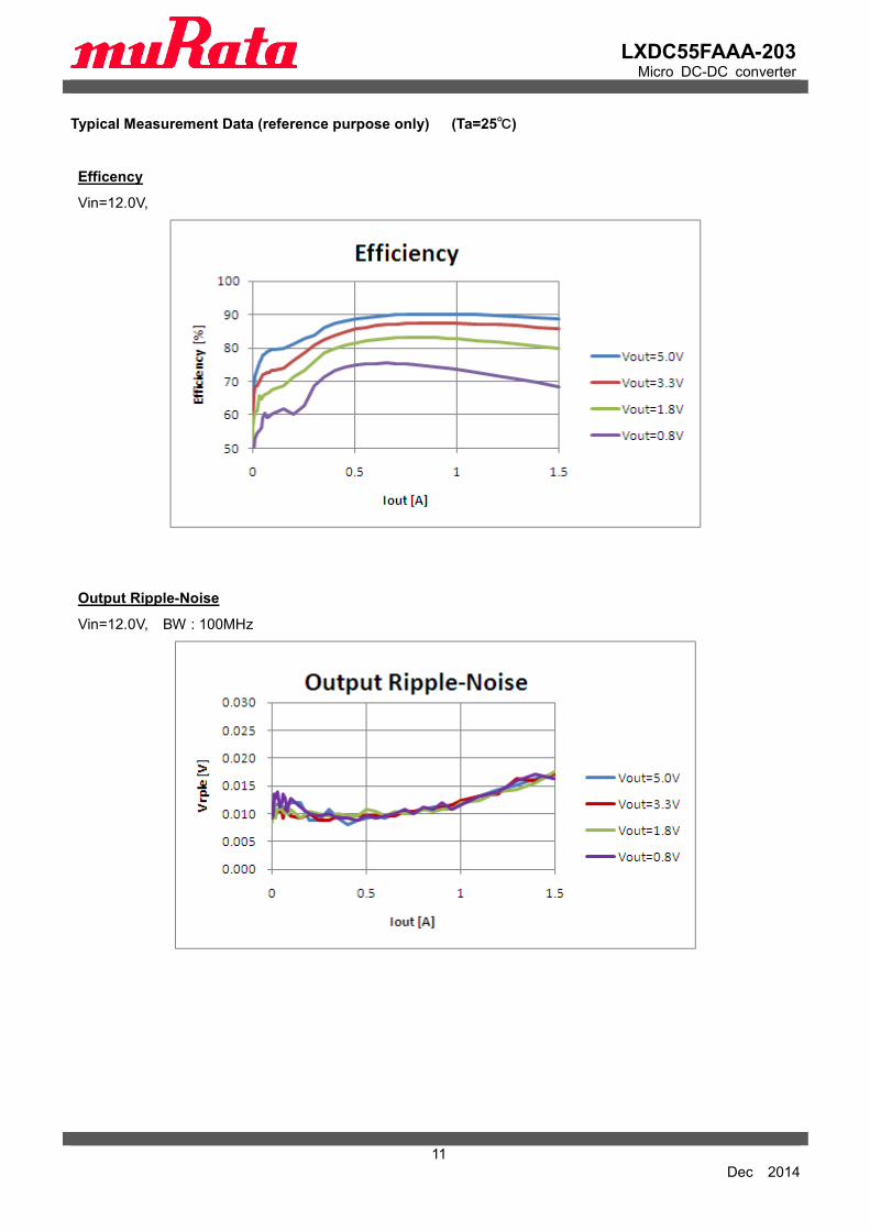
Typical Measurement Data (reference purpose only) (Ta=25℃)
Efficency
Vin=12.0V,
Output Ripple-Noise
Vin=12.0V, BW : 100MHz
LXDC55FAAA-203 Micro DC-DC converter
12
Dec 2014
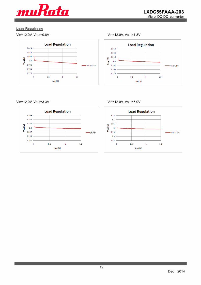
Load Regulation
Vin=12.0V, Vout=0.8V Vin=12.0V, Vout=1.8V
Vin=12.0V, Vout=3.3V Vin=12.0V, Vout=5.0V
LXDC55FAAA-203 Micro DC-DC converter
13
Dec 2014
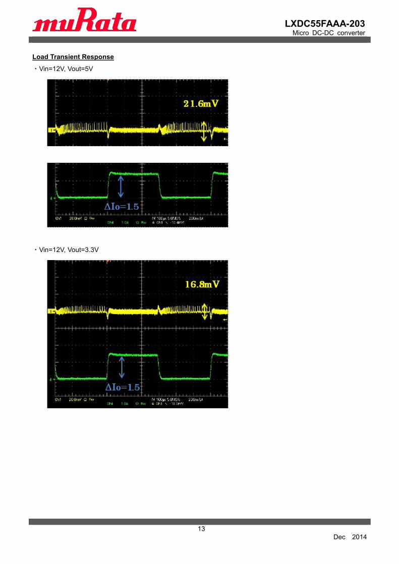
Load Transient Response
・Vin=12V, Vout=5V
・Vin=12V, Vout=3.3V

LXDC55FAAA-203 Micro DC-DC converter
14
Dec 2014
Start Up Waveform
・Vin=12V, Vout=5V
・Vin=12V, Vout=3.3V
LXDC55FAAA-203 Micro DC-DC converter
15
Dec 2014
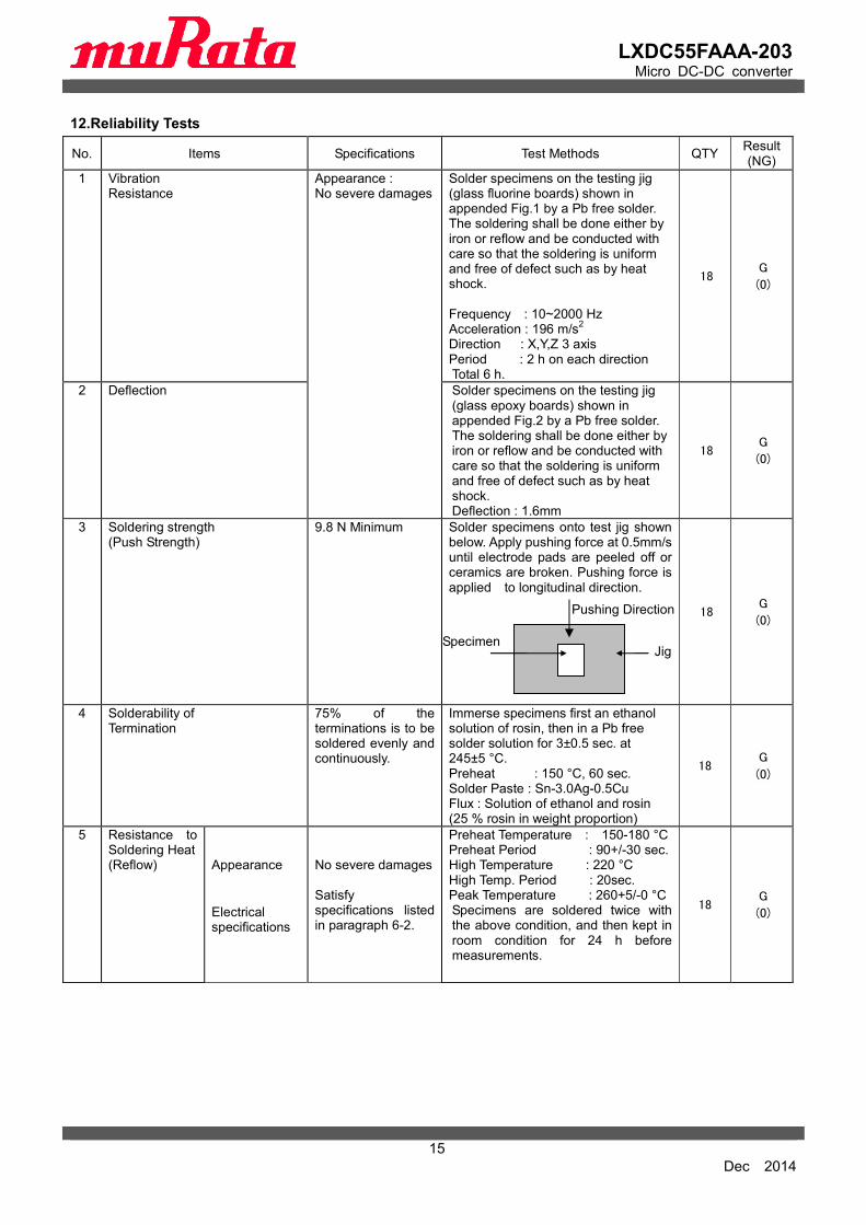
12.Reliability Tests
No. Items Specifications Test Methods QTY Result (NG)
1
Vibration Resistance
Appearance : No severe damages
Solder specimens on the testing jig (glass fluorine boards) shown in appended Fig.1 by a Pb free solder. The soldering shall be done either by iron or reflow and be conducted with care so that the soldering is uniform and free of defect such as by heat shock. Frequency : 10~2000 Hz Acceleration : 196 m/s2 Direction : X,Y,Z 3 axis Period : 2 h on each direction Total 6 h.
18 G
(0)
2 Deflection Solder specimens on the testing jig (glass epoxy boards) shown in appended Fig.2 by a Pb free solder. The soldering shall be done either by iron or reflow and be conducted with care so that the soldering is uniform and free of defect such as by heat shock. Deflection : 1.6mm
18 G
(0)
3 Soldering strength (Push Strength)
9.8 N Minimum Solder specimens onto test jig shown below. Apply pushing force at 0.5mm/s until electrode pads are peeled off or ceramics are broken. Pushing force is applied to longitudinal direction.
18 G
(0)
4 Solderability of Termination
75% of the terminations is to be soldered evenly and continuously.
Immerse specimens first an ethanol solution of rosin, then in a Pb free solder solution for 3±0.5 sec. at 245±5 °C. Preheat : 150 °C, 60 sec. Solder Paste : Sn-3.0Ag-0.5Cu Flux : Solution of ethanol and rosin (25 % rosin in weight proportion)
18 G
(0)
5 Resistance to Soldering Heat (Reflow)
Appearance Electrical specifications
No severe damages Satisfy specifications listed in paragraph 6-2.
Preheat Temperature : 150-180 °C Preheat Period : 90+/-30 sec. High Temperature : 220 °C High Temp. Period : 20sec. Peak Temperature : 260+5/-0 °C Specimens are soldered twice with the above condition, and then kept in room condition for 24 h before measurements.
18 G
(0)
Pushing Direction
Jig Specimen

LXDC55FAAA-203 Micro DC-DC converter
16
Dec 2014
No. Items Specifications Test Methods QTY Result (NG)
6 High Temp. Exposure
Appearance Electrical specifications
No severe damages Satisfy specifications listed in paragraph 6-2.
Temperature:85±2 ℃ Period:1000+48/-0 h Room Condition:2~24h
18 G (0)
7 Temperature Cycle
Condition:100 cycles in the following table
Step Temp(°C) Time(min)
1 Min.
Operating Temp.+0/-3
30±3
2 Max.
Operating Temp.+3/-0
30±3
18 G (0)
8 Humidity (Steady State)
Temperature:85±2 ℃ Humidity:80~90%RH Period:1000+48/-0 h Room Condition:2~24h
18 G (0)
9 Low Temp. Exposure
Temperature:-40±2 ℃ Period:1000+48/-0 h Room Condition:2~24h 18 G
(0)
10
ESD(Machine Model)
C:200pF、R:0Ω TEST Voltage :+/-100V Number of electric discharges:1
5 G (0)
11
ESD(Human Body Model)
C:100pF、R:1500Ω TEST Voltage :+/-1000V Number of electric discharges:1
5 G (0)

LXDC55FAAA-203 Micro DC-DC converter
17
Dec 2014
13. Tape and Reel Packing
1)Dimensions of Tape (Plastic tape)
2) Dimensions of Reel
(Unit : mm)
(Unit : mm)
(13.5)
2±0.5
17.5±1.0
φ13±0.2
Φ100 Φ330
Feeding direction

LXDC55FAAA-203 Micro DC-DC converter
18
Dec 2014
3) PACKAGE Diagrams (Humidity proof Packing)
Tape and reel must be sealed with the anti-humidity plastic bag. The bag contains the desiccant and the humidity
indicator.
4) Taping Diagrams(LXDC55F)
[1] Feeding Hole : As specified in (1)
[2] Hole for chip : As specified in (1)
[3] Cover tape : 50um in thickness
[4] Base tape : As specified in (1)
Feeding hole
Feedeng Direction
1pin Mark
湿度インジケ-タ
乾燥剤
表示ラべル
防湿梱包袋
表示ラベルLabel
Label
Desiccant
Humidity Indicator
Anti-humidity Aluminum foil pack
[1]
[2]
[3]
[3]
[4]
Chip

LXDC55FAAA-203 Micro DC-DC converter
19
Dec 2014
5) Leader and Tail tape
6) The tape for chips are wound clockwise, the feeding holes to the right side as the tape is pulled toward the user. 7) Packaging unit: 1,000pcs./ reel 8)Material : Base tape ...... Plastic Reel and Cover tape ......Plastic Base tape, Reel and Cover tape have an anti-ESD function. 9) Peeling of force : 0.1~1.3 N in the direction of peeling as shown below.
Tail tape(No components) Components No components
Feeding direction
Leader tape (Cover tape alone)
Over160mOver100mm
Over400mm
0.7N max
Base tape
0.1~1.3N
165 ~ 180 ° Cover tape

LXDC55FAAA-203 Micro DC-DC converter
20
Dec 2014
NOTICE 1. Storage Conditions: ・The product shall be stored without opening the packing under the ambient temperature from 5 to 35 deg.C
and humidity from 20 to 70%RH. (Packing materials, in particular, may be deformed at the temperature over 40 deg.C.) ・The product left more than 6 months after reception, it needs to be confirmed the solderbility before used.
- The product shall be stored in non corrosive gas (Cl2, NH3, SO2, Nox, etc.). - Any excess mechanical shock including, but not limited to, sticking the packing materials by sharp object and dropping the product, shall not be applied in order not to damage the packing materials.
・After the packing opened, the product shall be stored at < 30 deg.C / < 60 %RH and the product shall be
used within 168 hours. When the color of the indicator in the packing changed, the product shall be baked before soldering.
This product is applicable to MSL3 (Based on IPC/JEDEC J-STD-020)
2. Handling Conditions:
Be careful in handling or transporting the product. Excessive stress or mechanical shock may damage the product because of the nature of ceramics structure. Do not touch the product, especially the terminals, with bare hands. Doing so may result in poor solderability.
3. Standard PCB Design (Land Pattern and Dimensions):
All the ground terminals should be connected to ground patterns. Furthermore, the ground pattern should be provided between IN and OUT terminals. Please refer to the specifications for the standard land dimensions.
The recommended land pattern and dimensions are shown for a reference purpose only. Electrical, mechanical and thermal characteristics of the product shall depend on the pattern design and material / thickness of the PCB. Therefore, be sure to check the product performance in the actual set. When using underfill materials, be sure to check the mechanical characteristics in the actual set.

LXDC55FAAA-203 Micro DC-DC converter
21
Dec 2014
4. Soldering Conditions: Soldering is allowed up through 2 times. Carefully perform preheating :△T less than 130 °C. When products are immersed in solvent after mounting, pay special attention to maintain the temperature difference within 100 °C. Soldering must be carried out by the above mentioned conditions to prevent products from damage. Contact Murata before use if concerning other soldering conditions.
Use rosin type flux or weakly active flux with a chlorine content of 0.2 wt % or less.
Reflow soldering standard conditions (example)
LXDC55FAAA-203 Micro DC-DC converter
22
Dec 2014
5. Cleaning Conditions: The product is not designed to be cleaned after soldering.
6. Operational Environment Conditions: Products are designed to work for electronic products under normal environmental conditions (ambient temperature, humidity and pressure). Therefore, products have no problems to be used under the similar conditions to the above-mentioned. However, if products are used under the following circumstances, it may damage products and leakage of electricity and abnormal temperature may occur.
- In an atmosphere containing corrosive gas ( Cl2, NH3, SOx, NOx etc.).
- In an atmosphere containing combustible and volatile gases. - In a dusty environment. - Direct sunlight - Water splashing place.
- Humid place where water condenses. - In a freezing environment.
If there are possibilities for products to be used under the preceding clause, consult with Murata before actual use. If static electricity is added to this product, degradation and destruction may be produced. Please use it after consideration enough so that neither static electricity nor excess voltage is added at the time of an assembly and measurement. If product malfunctions may result in serious damage, including that to human life, sufficient fail-safe
measures must be taken, including the following:
(1) Installation of protection circuits or other protective device to improve system safety (2) Installation of redundant circuits in the case of single-circuit failure
7. Input Power Capacity: Products shall be used in the input power capacity as specified in this specifications. Inform Murata beforehand, in case that the components are used beyond such input power capacity range.
LXDC55FAAA-203 Micro DC-DC converter
23
Dec 2014
8. Limitation of Applications: The products are designed and produced for application in ordinary electronic equipment (AV equipment, OA equipment, telecommunication, etc). If the products are to be used in devices requiring extremely high reliability following the application listed below, you should consult with the Murata staff in advance. - Aircraft equipment. - Aerospace equipment - Undersea equipment. - Power plant control equipment. - Medical equipment. - Transportation equipment (vehicles, trains, ships, etc.). - Automobile equipment which includes the genuine brand of car manufacture, car factory-installed option and dealer-installed option.
- Traffic signal equipment. - Disaster prevention / crime prevention equipment. - Data-procession equipment. - Application which malfunction or operational error may endanger human life and property of assets. - Application which related to occurrence the serious damage - Application of similar complexity and/ or reliability requirements to the applications listed in the above.
! Note: Please make sure that your product has been evaluated and confirmed against your specifications when our product is mounted to your product. Product specifications are subject to change or our products in it may be discontinued without advance notice. This catalog is for reference only and not an official product specification document, therefore, please review and approve our official product specification before ordering this product.