LN18 Arithmetic
21
1 NTUEE C.M. Li Logic Design Switc hing Circuits & Logic Design 電路與邏輯設計 Professor Chien-Mo James Li 李建模 Graduate Institute of Electronics Engin eerin g National Taiwan University Circuits for Arith metic Operations 2 NTUEE C.M. Li Logic Design Obj ect iv e of t hi s Chapter • Lea rn how to design a sequential cir cuit for arithmetic c alculation
-
date post
06-Jan-2016 -
Category
Documents
-
view
213 -
download
0
description
交換電路
Transcript of LN18 Arithmetic
7/17/2019 LN18 Arithmetic
http://slidepdf.com/reader/full/ln18-arithmetic 1/21
1NTUEE C.M. LiLogic Design
Switching Circuits & Logic Design 電路與邏輯設計
Professor Chien-Mo James Li 李建模Graduate Insti tute of Electronics Engineering
National Taiwan University
Circuits for Arithmetic Operations
2NTUEE C.M. LiLogic Design
Objective of this Chapter
• Learn how to design a sequential circuit for arithmetic calculation

7/17/2019 LN18 Arithmetic
http://slidepdf.com/reader/full/ln18-arithmetic 2/21
3NTUEE C.M. LiLogic Design
Outline
• Serial Adder with Accumulator
• Multiplier
• Divider
4NTUEE C.M. LiLogic Design
Review: Serial Adder
• What is serial adder?
♦ Add two numbers one bit by one bit
♦ Fig 13-12
Fig. 13-12

7/17/2019 LN18 Arithmetic
http://slidepdf.com/reader/full/ln18-arithmetic 3/21
5NTUEE C.M. LiLogic Design
Review: State Table of SA
• Fig 13-12 (b)x i y i c i c i+1 s i
0 0 0 0 0
0 0 1 0 1
0 1 0 0 1
0 1 1 1 0
1 0 0 0 1
1 0 1 1 0
1 1 0 1 0
1 1 1 1 1
6NTUEE C.M. LiLogic Design
Review: Timing Chart of SA
7/17/2019 LN18 Arithmetic
http://slidepdf.com/reader/full/ln18-arithmetic 4/21
7NTUEE C.M. LiLogic Design
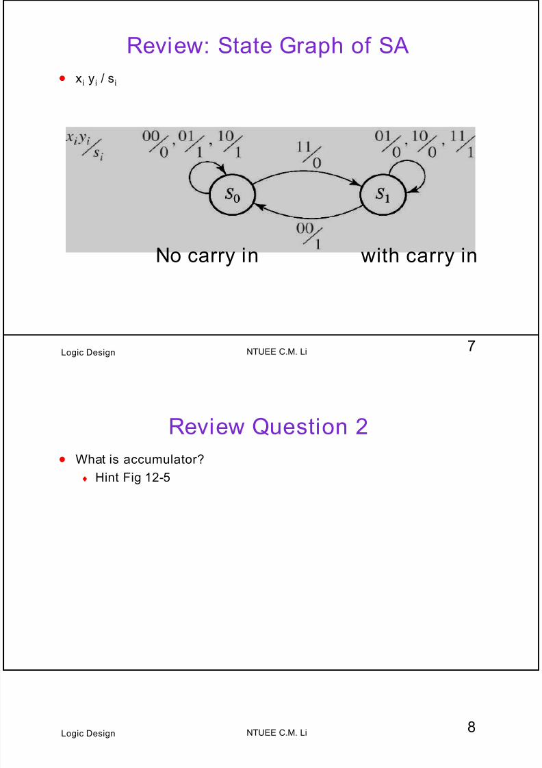
Review: State Graph of SA
• x i y i / si
No carry in with carry in
8NTUEE C.M. LiLogic Design
Review Question 2
• What is accumulator?
♦ Hint Fig 12-5
7/17/2019 LN18 Arithmetic
http://slidepdf.com/reader/full/ln18-arithmetic 5/21
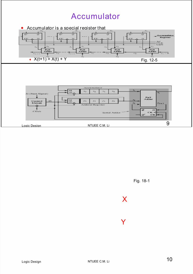
9NTUEE C.M. LiLogic Design
Accumulator
• Accumulator is a special register that
♦ Stores one number
♦ a second number can be added to it, leaving the result stored in
the same register • Fig 12-5: N-bit Parallel Adder with Accumulator
♦ X(t+1) = X(t) + Y Fig. 12-5
10NTUEE C.M. LiLogic Design
New: Serial Adder with Acc.
• Fig 18-1: block diagram for a serial adder wi th Acc.
♦ Add 4-bit X and 4-bit Y, one bit at a clock
♦ Result stored in X (accumulator)
Y
X
Fig. 18-1
7/17/2019 LN18 Arithmetic
http://slidepdf.com/reader/full/ln18-arithmetic 6/21
11NTUEE C.M. LiLogic Design
Four Blocks
• X is serial accumulator
• Y is cyclic shifter (Q: what is cycl ic shif ter?)
• serial adder
• Control Circuit
Serial adder
Cyclic Shifter
Accumulator
control
12NTUEE C.M. LiLogic Design
Serial Accumulator
• Control signal
♦ Sh: Shift signal
• Data input
♦ SI: serial input
• Data output
♦ SO: serial output
• Function
♦ Store X
♦ Store Sum
7/17/2019 LN18 Arithmetic
http://slidepdf.com/reader/full/ln18-arithmetic 7/21
13NTUEE C.M. LiLogic Design
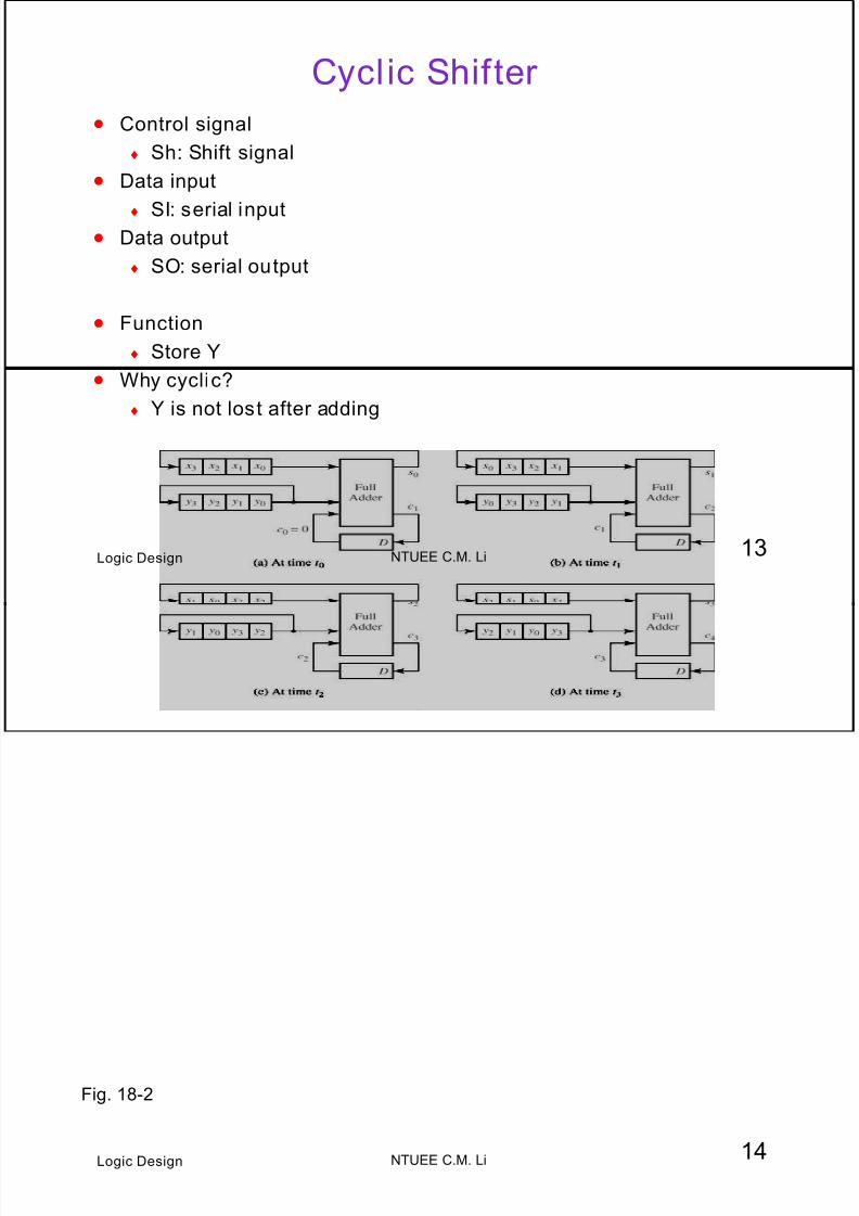
Cyclic Shifter
• Control signal
♦ Sh: Shift signal
• Data input
♦ SI: serial input• Data output
♦ SO: serial output
• Function
♦ Store Y
• Why cyclic?
♦ Y is not lost after adding
14NTUEE C.M. LiLogic Design
Operation of Serial Adder
Fig. 18-2
7/17/2019 LN18 Arithmetic
http://slidepdf.com/reader/full/ln18-arithmetic 8/21
15NTUEE C.M. LiLogic Design
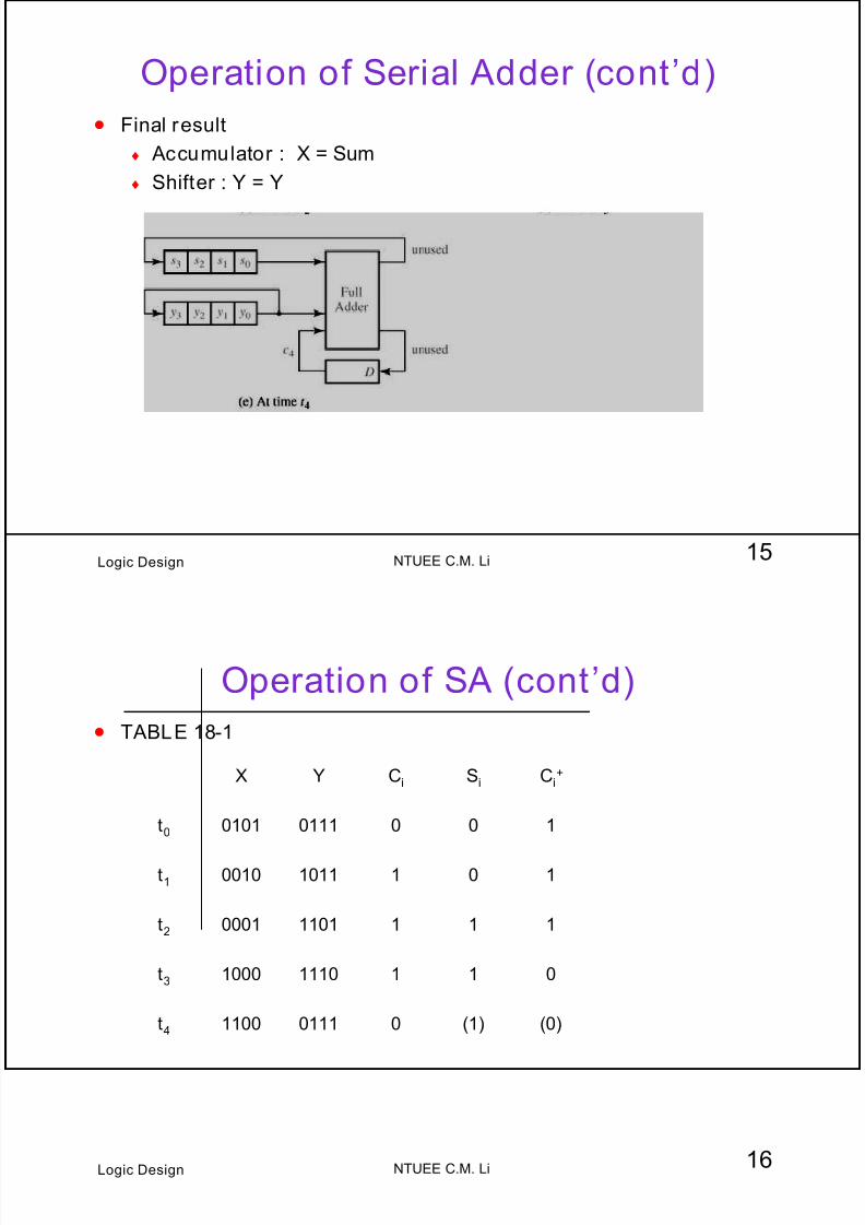
Operation of Serial Adder (cont’d)
• Final result
♦ Accumulator : X = Sum
♦ Shifter : Y = Y
16NTUEE C.M. LiLogic Design
Operation of SA (cont’d)
• TABLE 18-1
X Y Ci Si Ci+
t0 0101 0111 0 0 1
t1 0010 1011 1 0 1
t2 0001 1101 1 1 1
t3 1000 1110 1 1 0
t4 1100 0111 0 (1) (0)
7/17/2019 LN18 Arithmetic
http://slidepdf.com/reader/full/ln18-arithmetic 9/21
17NTUEE C.M. LiLogic Design
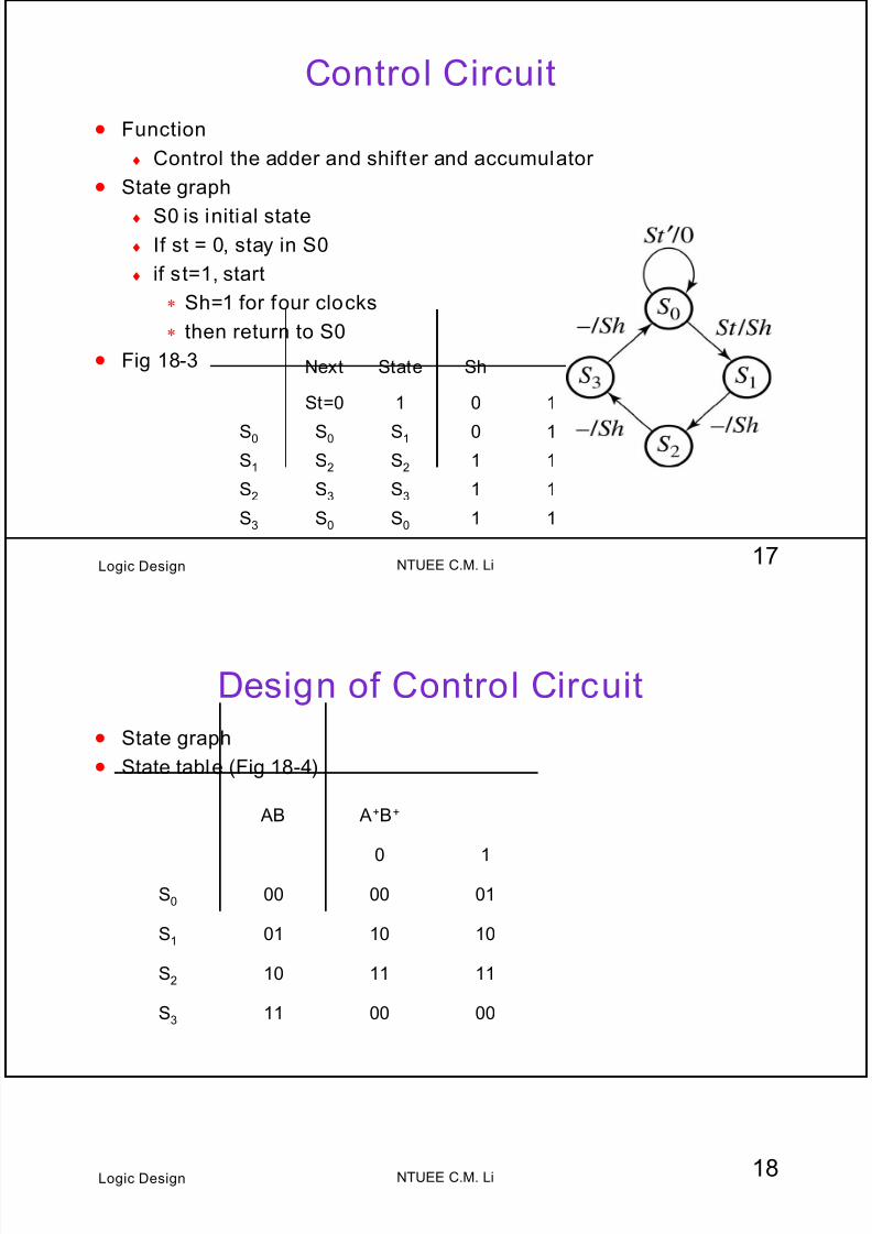
Control Circuit
• Function
♦ Control the adder and shifter and accumulator
• State graph
♦ S0 is initial state♦ If st = 0, stay in S0
♦ if st=1, start
∗ Sh=1 for four clocks
∗ then return to S0
• Fig 18-3 Next State Sh
St=0 1 0 1
S0 S0 S1 0 1S1 S2 S2 1 1
S2 S3 S3 1 1
S3 S0 S0 1 1
18NTUEE C.M. LiLogic Design
Design of Control Circuit
• State graph
• State table (Fig 18-4)
AB A+B+
0 1
S0 00 00 01
S1 01 10 10
S2 10 11 11
S3 11 00 00
7/17/2019 LN18 Arithmetic
http://slidepdf.com/reader/full/ln18-arithmetic 10/21
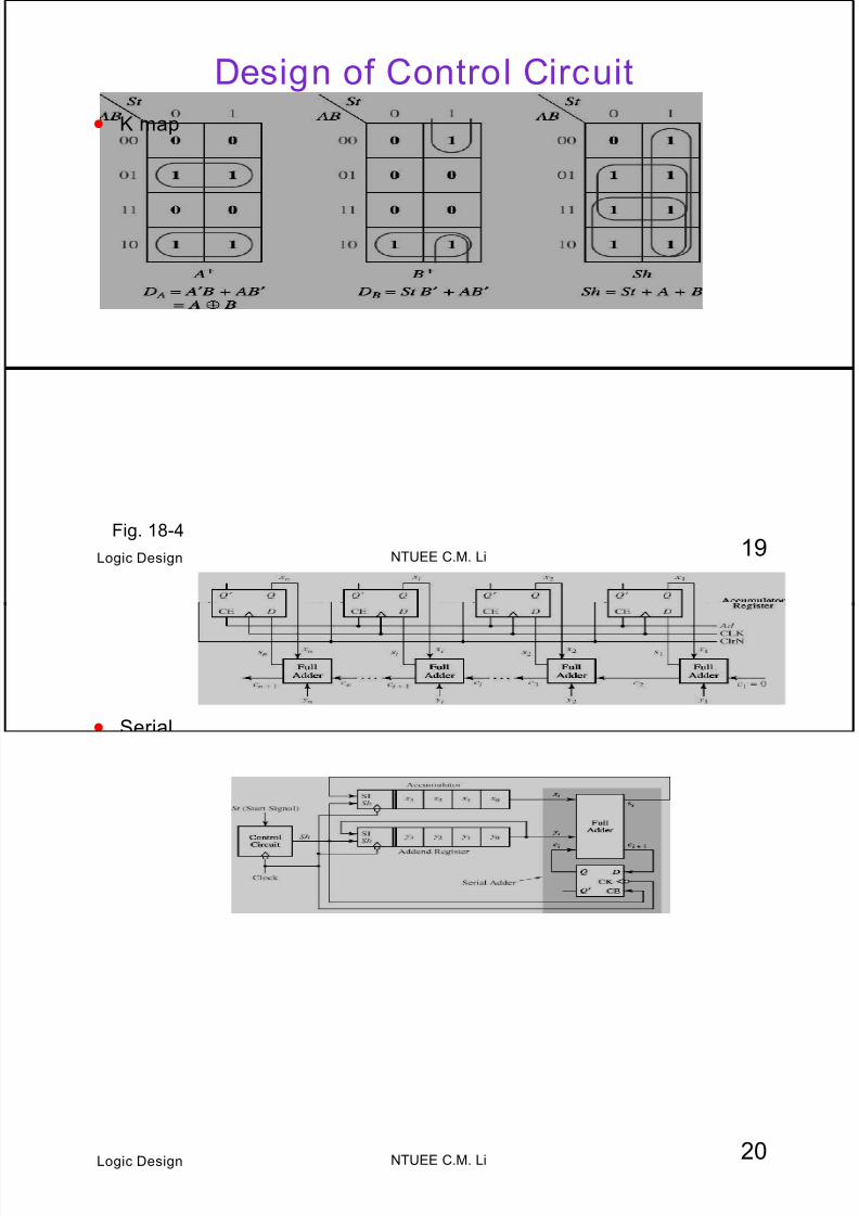
19NTUEE C.M. LiLogic Design
Design of Control Circuit
• K map
Fig. 18-4
20NTUEE C.M. LiLogic Design
FFT: Which is better?
• Serial
• parallel
Fig. 18-1
7/17/2019 LN18 Arithmetic
http://slidepdf.com/reader/full/ln18-arithmetic 11/21
21NTUEE C.M. LiLogic Design
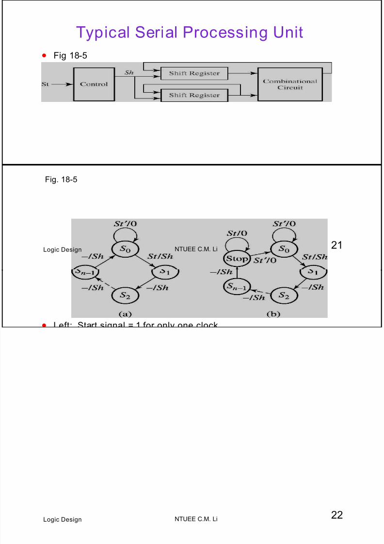
Typical Serial Processing Unit
• Fig 18-5
Fig. 18-5
22NTUEE C.M. LiLogic Design
State Graph of Control
• Left: Start signal = 1 for only one clock
• Right : start signal = 1 1 1 1 … 1 ->0
♦ An extra stop state is added
7/17/2019 LN18 Arithmetic
http://slidepdf.com/reader/full/ln18-arithmetic 12/21
23NTUEE C.M. LiLogic Design
Outline
• Serial Adder with Accumulator
• Multiplier
• Divider
24NTUEE C.M. LiLogic Design
Binary Multiplication
• How do you perform binary multiplication?
♦ p. 542

7/17/2019 LN18 Arithmetic
http://slidepdf.com/reader/full/ln18-arithmetic 13/21
25NTUEE C.M. LiLogic Design
Block Diagram for Parallel Mult ipl ier
• Fig 18-7
Fig. 18-7
26NTUEE C.M. LiLogic Design
How is Multiplication done?
• P. 600
7/17/2019 LN18 Arithmetic
http://slidepdf.com/reader/full/ln18-arithmetic 14/21
27NTUEE C.M. LiLogic Design
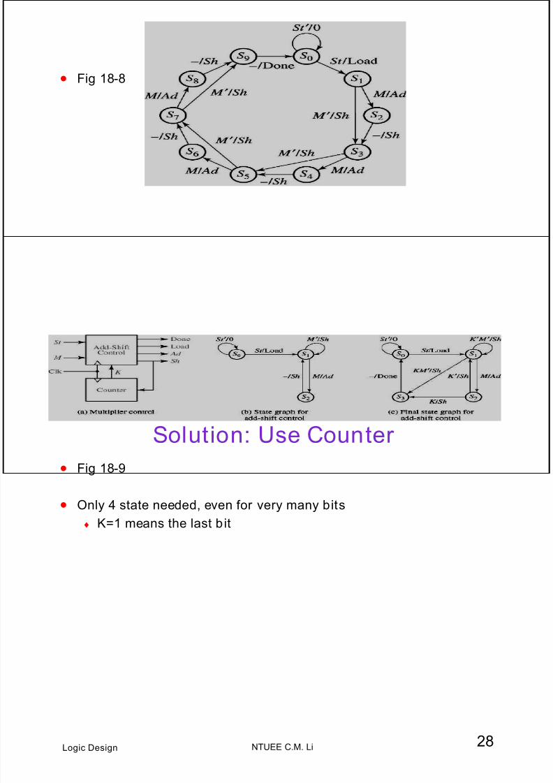
Controller State Graph
• Fig 18-8
• Problems:
♦ Too many states
♦ not flexible
Fig. 18-8
28NTUEE C.M. LiLogic Design
Solution: Use Counter
• Fig 18-9
• Only 4 state needed, even for very many bits
♦ K=1 means the last bit
7/17/2019 LN18 Arithmetic
http://slidepdf.com/reader/full/ln18-arithmetic 15/21
29NTUEE C.M. LiLogic Design
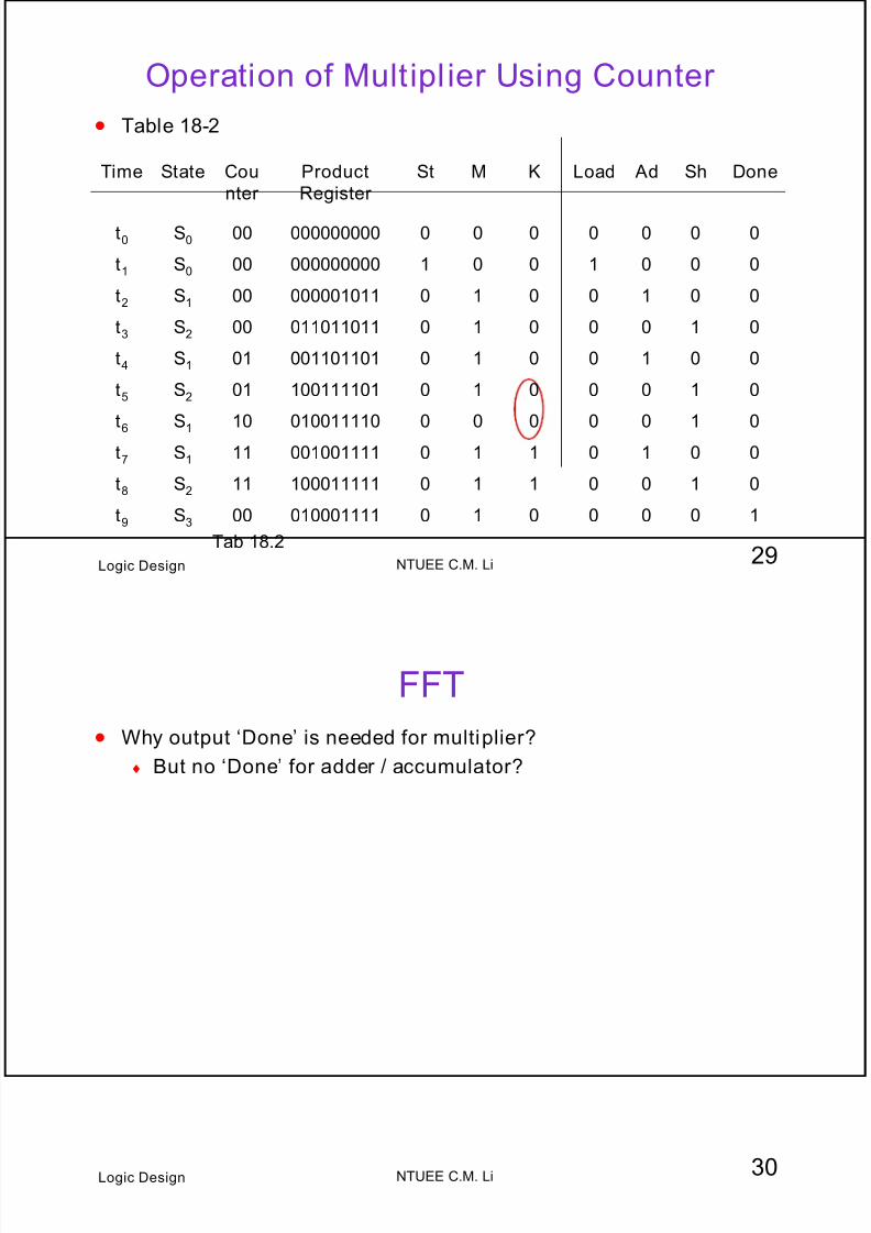
Operation of Multipl ier Using Counter
• Table 18-2
Time State Cou
nter
Product
Register
St M K Load Ad Sh Done
t0 S0 00 000000000 0 0 0 0 0 0 0
t1 S0 00 000000000 1 0 0 1 0 0 0
t2 S1 00 000001011 0 1 0 0 1 0 0
t3 S2 00 011011011 0 1 0 0 0 1 0
t4 S1 01 001101101 0 1 0 0 1 0 0
t5 S2 01 100111101 0 1 0 0 0 1 0
t6
S1
10 010011110 0 0 0 0 0 1 0
t7 S1 11 001001111 0 1 1 0 1 0 0
t8 S2 11 100011111 0 1 1 0 0 1 0
t9 S3 00 010001111 0 1 0 0 0 0 1
Tab 18.2
30NTUEE C.M. LiLogic Design
FFT
• Why output ‘Done’ is needed for multiplier?
♦ But no ‘Done’ for adder / accumulator?
7/17/2019 LN18 Arithmetic
http://slidepdf.com/reader/full/ln18-arithmetic 16/21
31NTUEE C.M. LiLogic Design
Outline
• Serial Adder with Accumulator
• Multiplier
• Divider
32NTUEE C.M. LiLogic Design
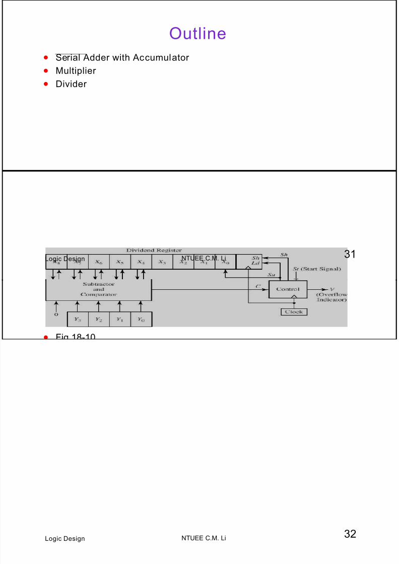
Parallel Binary Divider
• Fig 18-10
♦ 9-bit dividend
♦ 4-bit divisor
♦ 4-bit quotient
♦ 4-bit remainder Fig. 18-10
7/17/2019 LN18 Arithmetic
http://slidepdf.com/reader/full/ln18-arithmetic 17/21
33NTUEE C.M. LiLogic Design
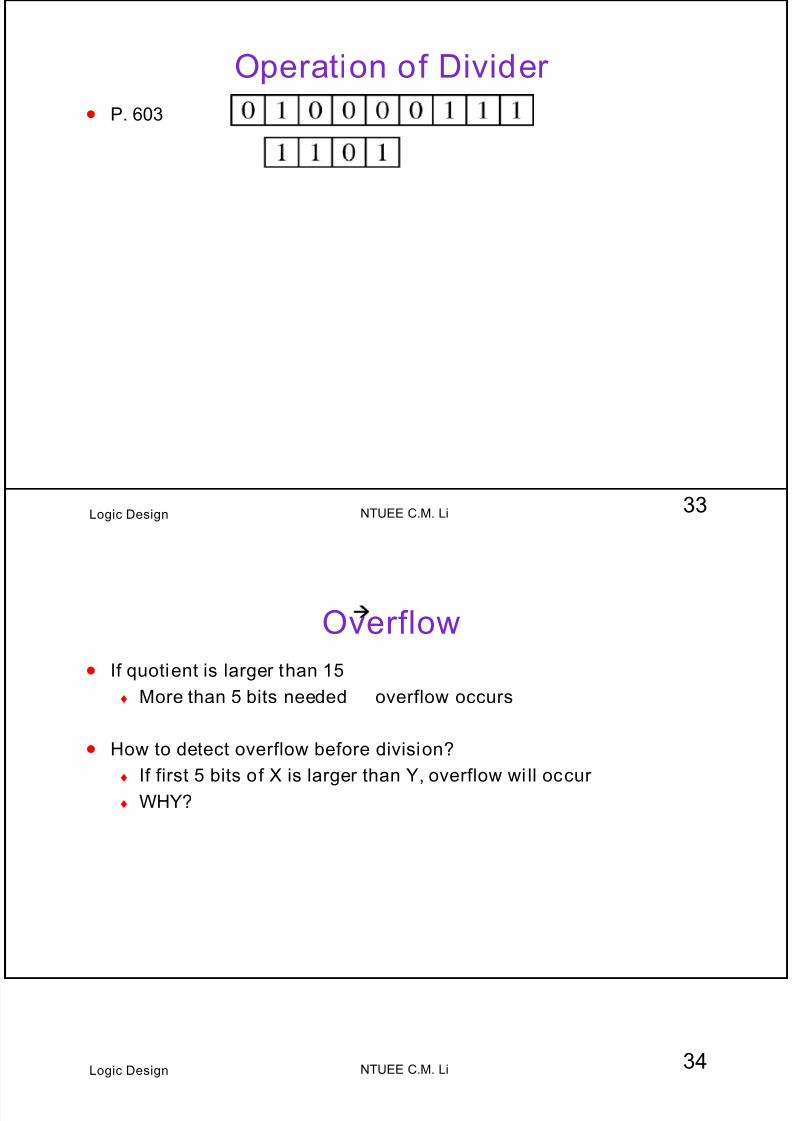
Operation of Divider
• P. 603
34NTUEE C.M. LiLogic Design
Overflow
• If quotient is larger than 15
♦ More than 5 bits needed overflow occurs
• How to detect overflow before division?
♦ If first 5 bits of X is larger than Y, overflow wi ll occur
♦ WHY?
7/17/2019 LN18 Arithmetic
http://slidepdf.com/reader/full/ln18-arithmetic 18/21
35NTUEE C.M. LiLogic Design
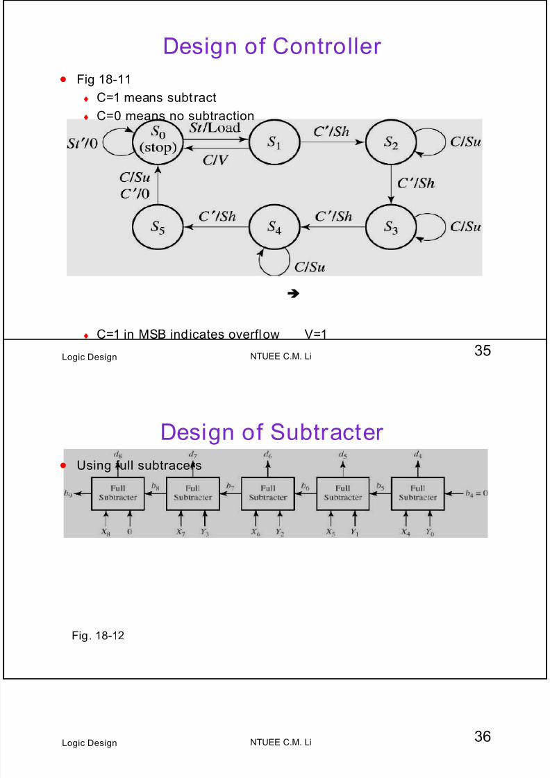
Design of Controller
• Fig 18-11
♦ C=1 means subtract
♦ C=0 means no subtraction
♦ C=1 in MSB indicates overflow V=1
36NTUEE C.M. LiLogic Design
Design of Subtracter
• Using full subtracers
Fig. 18-12
7/17/2019 LN18 Arithmetic
http://slidepdf.com/reader/full/ln18-arithmetic 19/21
37NTUEE C.M. LiLogic Design
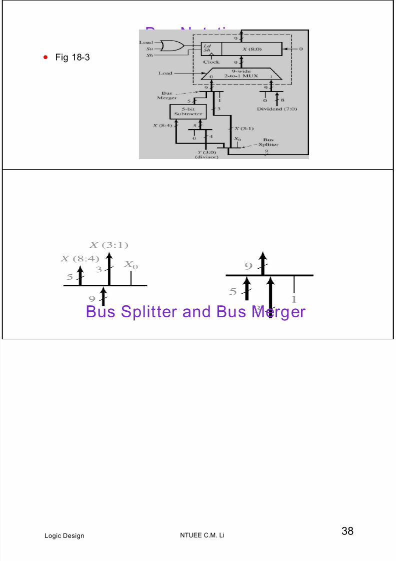
Bus Notation
• Fig 18-3
Fig. 18-3
38NTUEE C.M. LiLogic Design
Bus Splitter and Bus Merger
7/17/2019 LN18 Arithmetic
http://slidepdf.com/reader/full/ln18-arithmetic 20/21
39NTUEE C.M. LiLogic Design
FFT
• Compare Fig 18-3 with 18-10. Should we tie Load and Su together?
40NTUEE C.M. LiLogic Design
What’s Next After Logic Design?
• NTU undergrad.
♦ Digital circuit Lab
♦ Introduct ion to VLSI
♦ Algorithm
♦ Data structure
♦ Introduct ion to EDA
♦ Computer Architecture
• GIEE
♦ Advanced VLSI Design
♦ Computer Aided VLSI System Design
♦ VLSI Testing
7/17/2019 LN18 Arithmetic
http://slidepdf.com/reader/full/ln18-arithmetic 21/21
41NTUEE C.M. LiLogic Design
End of Logic Design
• Good luck on Final