LM34 Precision Fahrenheit Temperature Sensors (Rev. D) · PDF fileLM34 SNIS161D–MARCH...
30
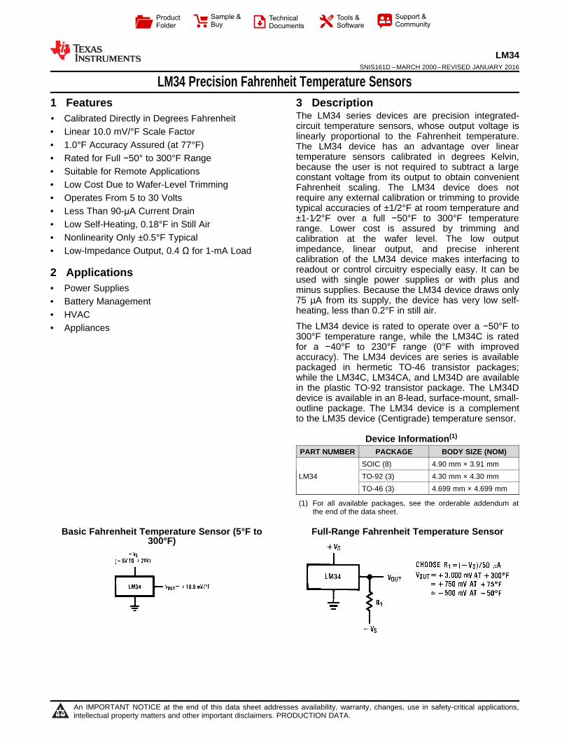
Product Folder Sample & Buy Technical Documents Tools & Software Support & Community LM34 SNIS161D – MARCH 2000 – REVISED JANUARY 2016 LM34 Precision Fahrenheit Temperature Sensors 1 Features 3 Description The LM34 series devices are precision integrated- 1• Calibrated Directly in Degrees Fahrenheit circuit temperature sensors, whose output voltage is • Linear 10.0 mV/°F Scale Factor linearly proportional to the Fahrenheit temperature. • 1.0°F Accuracy Assured (at 77°F) The LM34 device has an advantage over linear temperature sensors calibrated in degrees Kelvin, • Rated for Full −50° to 300°F Range because the user is not required to subtract a large • Suitable for Remote Applications constant voltage from its output to obtain convenient • Low Cost Due to Wafer-Level Trimming Fahrenheit scaling. The LM34 device does not require any external calibration or trimming to provide • Operates From 5 to 30 Volts typical accuracies of ±1/2°F at room temperature and • Less Than 90-μA Current Drain ±1-1⁄2°F over a full −50°F to 300°F temperature • Low Self-Heating, 0.18°F in Still Air range. Lower cost is assured by trimming and • Nonlinearity Only ±0.5°F Typical calibration at the wafer level. The low output impedance, linear output, and precise inherent • Low-Impedance Output, 0.4 Ω for 1-mA Load calibration of the LM34 device makes interfacing to readout or control circuitry especially easy. It can be 2 Applications used with single power supplies or with plus and • Power Supplies minus supplies. Because the LM34 device draws only 75 μA from its supply, the device has very low self- • Battery Management heating, less than 0.2°F in still air. • HVAC The LM34 device is rated to operate over a −50°F to • Appliances 300°F temperature range, while the LM34C is rated for a −40°F to 230°F range (0°F with improved accuracy). The LM34 devices are series is available packaged in hermetic TO-46 transistor packages; while the LM34C, LM34CA, and LM34D are available in the plastic TO-92 transistor package. The LM34D device is available in an 8-lead, surface-mount, small- outline package. The LM34 device is a complement to the LM35 device (Centigrade) temperature sensor. Device Information (1) PART NUMBER PACKAGE BODY SIZE (NOM) SOIC (8) 4.90 mm × 3.91 mm LM34 TO-92 (3) 4.30 mm × 4.30 mm TO-46 (3) 4.699 mm × 4.699 mm (1) For all available packages, see the orderable addendum at the end of the data sheet. Basic Fahrenheit Temperature Sensor (5°F to Full-Range Fahrenheit Temperature Sensor 300°F) 1 An IMPORTANT NOTICE at the end of this data sheet addresses availability, warranty, changes, use in safety-critical applications, intellectual property matters and other important disclaimers. PRODUCTION DATA.
-
Upload
hoangthien -
Category
Documents
-
view
213 -
download
0
Transcript of LM34 Precision Fahrenheit Temperature Sensors (Rev. D) · PDF fileLM34 SNIS161D–MARCH...
Product
Folder
Sample &Buy
Technical
Documents
Tools &
Software
Support &Community
LM34SNIS161D –MARCH 2000–REVISED JANUARY 2016
LM34 Precision Fahrenheit Temperature Sensors1 Features 3 Description
The LM34 series devices are precision integrated-1• Calibrated Directly in Degrees Fahrenheit
circuit temperature sensors, whose output voltage is• Linear 10.0 mV/°F Scale Factor linearly proportional to the Fahrenheit temperature.• 1.0°F Accuracy Assured (at 77°F) The LM34 device has an advantage over linear
temperature sensors calibrated in degrees Kelvin,• Rated for Full −50° to 300°F Rangebecause the user is not required to subtract a large• Suitable for Remote Applications constant voltage from its output to obtain convenient
• Low Cost Due to Wafer-Level Trimming Fahrenheit scaling. The LM34 device does notrequire any external calibration or trimming to provide• Operates From 5 to 30 Voltstypical accuracies of ±1/2°F at room temperature and• Less Than 90-μA Current Drain±1-1⁄2°F over a full −50°F to 300°F temperature• Low Self-Heating, 0.18°F in Still Air range. Lower cost is assured by trimming and
• Nonlinearity Only ±0.5°F Typical calibration at the wafer level. The low outputimpedance, linear output, and precise inherent• Low-Impedance Output, 0.4 Ω for 1-mA Loadcalibration of the LM34 device makes interfacing toreadout or control circuitry especially easy. It can be2 Applicationsused with single power supplies or with plus and
• Power Supplies minus supplies. Because the LM34 device draws only75 µA from its supply, the device has very low self-• Battery Managementheating, less than 0.2°F in still air.• HVACThe LM34 device is rated to operate over a −50°F to• Appliances300°F temperature range, while the LM34C is ratedfor a −40°F to 230°F range (0°F with improvedaccuracy). The LM34 devices are series is availablepackaged in hermetic TO-46 transistor packages;while the LM34C, LM34CA, and LM34D are availablein the plastic TO-92 transistor package. The LM34Ddevice is available in an 8-lead, surface-mount, small-outline package. The LM34 device is a complementto the LM35 device (Centigrade) temperature sensor.
Device Information(1)
PART NUMBER PACKAGE BODY SIZE (NOM)SOIC (8) 4.90 mm × 3.91 mm
LM34 TO-92 (3) 4.30 mm × 4.30 mmTO-46 (3) 4.699 mm × 4.699 mm
(1) For all available packages, see the orderable addendum atthe end of the data sheet.
Basic Fahrenheit Temperature Sensor (5°F to Full-Range Fahrenheit Temperature Sensor300°F)
1
An IMPORTANT NOTICE at the end of this data sheet addresses availability, warranty, changes, use in safety-critical applications,intellectual property matters and other important disclaimers. PRODUCTION DATA.
LM34SNIS161D –MARCH 2000–REVISED JANUARY 2016 www.ti.com
Table of Contents7.3 Feature Description................................................. 111 Features .................................................................. 17.4 Device Functional Modes........................................ 122 Applications ........................................................... 1
8 Application and Implementation ........................ 133 Description ............................................................. 18.1 Application Information............................................ 134 Revision History..................................................... 28.2 Typical Application .................................................. 135 Pin Configuration and Functions ......................... 38.3 System Examples ................................................... 146 Specifications......................................................... 4
9 Power Supply Recommendations ...................... 166.1 Absolute Maximum Ratings ...................................... 410 Layout................................................................... 166.2 ESD Ratings.............................................................. 4
10.1 Layout Guidelines ................................................. 166.3 Recommended Operating Conditions....................... 410.2 Layout Example .................................................... 176.4 Thermal Information .................................................. 4
11 Device and Documentation Support ................. 186.5 Electrical Characteristics: LM34A and LM34CA ....... 511.1 Trademarks ........................................................... 186.6 Electrical Characteristics: LM34, LM34C, and
LM34D........................................................................ 7 11.2 Electrostatic Discharge Caution............................ 186.7 Typical Characteristics .............................................. 9 11.3 Glossary ................................................................ 18
7 Detailed Description ............................................ 11 12 Mechanical, Packaging, and OrderableInformation ........................................................... 187.1 Overview ................................................................. 11
7.2 Functional Block Diagram ....................................... 11
4 Revision History
Changes from Revision C (January 2015) to Revision D Page
• Changed NDV Package (TO-46) pinout from Top View to Bottom View ............................................................................... 3
Changes from Revision B (November 2000) to Revision C Page
• Added ESD Ratings table, Feature Description section, Device Functional Modes, Application and Implementationsection, Power Supply Recommendations section, Layout section, Device and Documentation Support section, andMechanical, Packaging, and Orderable Information section. ................................................................................................. 1
2 Submit Documentation Feedback Copyright © 2000–2016, Texas Instruments Incorporated
Product Folder Links: LM34
+VS VOUT GND
+VSVOUT
GND
N.C.
N.C.
N.C.
N.C.
N.C.
12
3
4
87
6
5
+VS VOUT
GND t
LM34www.ti.com SNIS161D –MARCH 2000–REVISED JANUARY 2016
5 Pin Configuration and Functions
NDV Package3-PIn TO-46
(Bottom View)
Case is connected to negative pin (GND)
D Package8-PIn SO8(Top View)
N.C. = No connection
LP Package3-Pin TO-92
(Bottom View)
Pin FunctionsPIN
TYPE DESCRIPTIONNAME TO46/NDV TO92/LP SO8/D+VS — — 8 POWER Positive power supply pinVOUT — — 1 O Temperature Sensor Analog OutputGND — — 4 GND Device ground pin, connect to power supply negative terminal
23
N.C. — — 5 — No Connection67
Copyright © 2000–2016, Texas Instruments Incorporated Submit Documentation Feedback 3
Product Folder Links: LM34
LM34SNIS161D –MARCH 2000–REVISED JANUARY 2016 www.ti.com
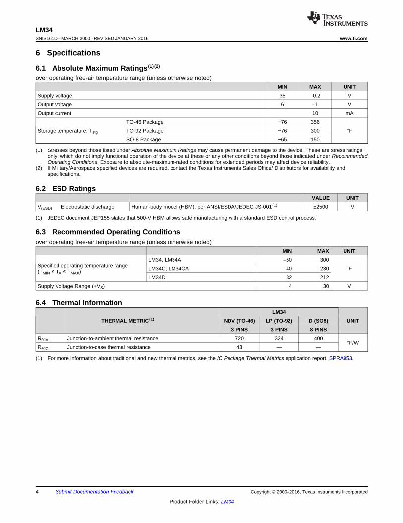
6 Specifications
6.1 Absolute Maximum Ratings (1) (2)
over operating free-air temperature range (unless otherwise noted)MIN MAX UNIT
Supply voltage 35 –0.2 VOutput voltage 6 –1 VOutput current 10 mA
TO-46 Package −76 356Storage temperature, Tstg TO-92 Package −76 300 °F
SO-8 Package −65 150
(1) Stresses beyond those listed under Absolute Maximum Ratings may cause permanent damage to the device. These are stress ratingsonly, which do not imply functional operation of the device at these or any other conditions beyond those indicated under RecommendedOperating Conditions. Exposure to absolute-maximum-rated conditions for extended periods may affect device reliability.
(2) If Military/Aerospace specified devices are required, contact the Texas Instruments Sales Office/ Distributors for availability andspecifications.
6.2 ESD RatingsVALUE UNIT
V(ESD) Electrostatic discharge Human-body model (HBM), per ANSI/ESDA/JEDEC JS-001 (1) ±2500 V
(1) JEDEC document JEP155 states that 500-V HBM allows safe manufacturing with a standard ESD control process.
6.3 Recommended Operating Conditionsover operating free-air temperature range (unless otherwise noted)
MIN MAX UNITLM34, LM34A –50 300
Specified operating temperature range LM34C, LM34CA –40 230 °F(TMIN ≤ TA ≤ TMAX)LM34D 32 212
Supply Voltage Range (+VS) 4 30 V
6.4 Thermal InformationLM34
THERMAL METRIC (1) NDV (TO-46) LP (TO-92) D (SO8) UNIT3 PINS 3 PINS 8 PINS
RθJA Junction-to-ambient thermal resistance 720 324 400°F/W
RθJC Junction-to-case thermal resistance 43 — —
(1) For more information about traditional and new thermal metrics, see the IC Package Thermal Metrics application report, SPRA953.
4 Submit Documentation Feedback Copyright © 2000–2016, Texas Instruments Incorporated
Product Folder Links: LM34

LM34www.ti.com SNIS161D –MARCH 2000–REVISED JANUARY 2016
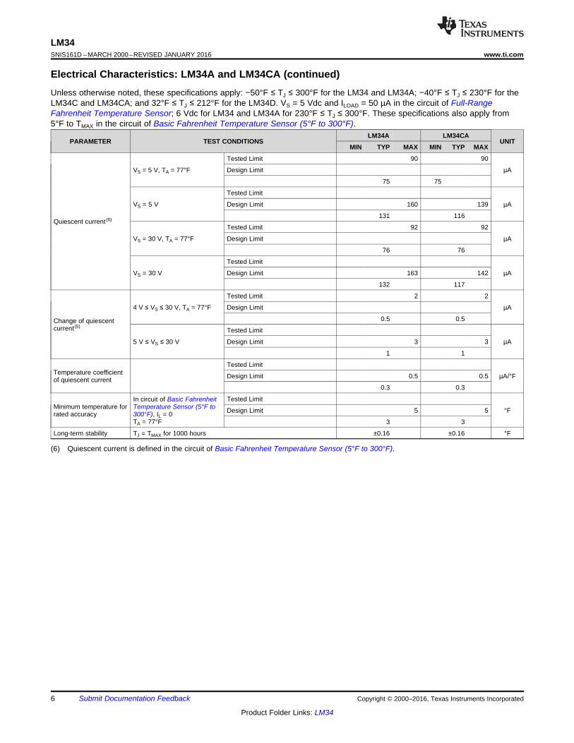
6.5 Electrical Characteristics: LM34A and LM34CAUnless otherwise noted, these specifications apply: −50°F ≤ TJ ≤ 300°F for the LM34 and LM34A; −40°F ≤ TJ ≤ 230°F for theLM34C and LM34CA; and 32°F ≤ TJ ≤ 212°F for the LM34D. VS = 5 Vdc and ILOAD = 50 µA in the circuit of Full-RangeFahrenheit Temperature Sensor; 6 Vdc for LM34 and LM34A for 230°F ≤ TJ ≤ 300°F. These specifications also apply from5°F to TMAX in the circuit of Basic Fahrenheit Temperature Sensor (5°F to 300°F).
LM34A LM34CAPARAMETER TEST CONDITIONS UNIT
MIN TYP MAX MIN TYP MAX
Tested Limit (2) –1 1 –1 1
TA = 77°F Design Limit (3) °F
±0.4 ±0.4
Tested Limit
T A = 0°F Design Limit –2 2 °F
±0.6 ±0.6Accuracy (1)
Tested Limit –2 2 –2 2
TA = TMAX Design Limit °F
±0.8 ±0.8
Tested Limit –2 2
TA = TMIN Design Limit –3 3 °F
±0.8 ±0.8
Tested Limit
Nonlinearity (4) Design Limit –0.7 0.7 –0.6 0.6 °F
TA = 77°F ±0.35 ±0.3
Tested Limit 9.9 10.1Sensor gain (Average Design Limit +9.9 10.1 mV/°FSlope)
TA = 77°F +10 10
Tested Limit –1 1 –1 1TA = 77°F Design Limit mV/mA0 ≤ IL ≤ 1 mA
±0.4 ±0.4Load regulation (5)
Tested Limit
0 ≤ IL ≤ 1 mA Design Limit –3 3 –3 3 mV/mA
±0.5 ±0.5
Tested Limit –0.05 0.05 –0.05 0.05TA = 77°F Design Limit mV/V5 V ≤ VS ≤ 30 V
±0.01 ±0.01Line regulation (5)
Tested Limit
5 V ≤ VS ≤ 30 V Design Limit –0.1 0.1 –0.1 0.1 mV/V
±0.02 ±0.02
(1) Accuracy is defined as the error between the output voltage and 10 mV/°F times the device’s case temperature at specified conditions ofvoltage, current, and temperature (expressed in °F).
(2) Tested limits are specified and 100% tested in production.(3) Design limits are specified (but not 100% production tested) over the indicated temperature and supply voltage ranges. These limits are
not used to calculate outgoing quality levels.(4) Nonlinearity is defined as the deviation of the output-voltage-versus-temperature curve from the best-fit straight line over the rated
temperature range of the device.(5) Regulation is measured at constant junction temperature using pulse testing with a low duty cycle. Changes in output due to heating
effects can be computed by multiplying the internal dissipation by the thermal resistance.
Copyright © 2000–2016, Texas Instruments Incorporated Submit Documentation Feedback 5
Product Folder Links: LM34
LM34SNIS161D –MARCH 2000–REVISED JANUARY 2016 www.ti.com
Electrical Characteristics: LM34A and LM34CA (continued)Unless otherwise noted, these specifications apply: −50°F ≤ TJ ≤ 300°F for the LM34 and LM34A; −40°F ≤ TJ ≤ 230°F for theLM34C and LM34CA; and 32°F ≤ TJ ≤ 212°F for the LM34D. VS = 5 Vdc and ILOAD = 50 µA in the circuit of Full-RangeFahrenheit Temperature Sensor; 6 Vdc for LM34 and LM34A for 230°F ≤ TJ ≤ 300°F. These specifications also apply from5°F to TMAX in the circuit of Basic Fahrenheit Temperature Sensor (5°F to 300°F).
LM34A LM34CAPARAMETER TEST CONDITIONS UNIT
MIN TYP MAX MIN TYP MAX
Tested Limit 90 90
VS = 5 V, TA = 77°F Design Limit µA
75 75
Tested Limit
VS = 5 V Design Limit 160 139 µA
131 116Quiescent current (6)
Tested Limit 92 92
VS = 30 V, TA = 77°F Design Limit µA
76 76
Tested Limit
VS = 30 V Design Limit 163 142 µA
132 117
Tested Limit 2 2
4 V ≤ VS ≤ 30 V, TA = 77°F Design Limit µA
0.5 0.5Change of quiescentcurrent (5)
Tested Limit
5 V ≤ VS ≤ 30 V Design Limit 3 3 µA
1 1
Tested LimitTemperature coefficient Design Limit 0.5 0.5 µA/°Fof quiescent current
0.3 0.3
Tested LimitIn circuit of Basic FahrenheitMinimum temperature for Temperature Sensor (5°F to Design Limit 5 5 °Frated accuracy 300°F), IL = 0
TA = 77°F 3 3
Long-term stability TJ = TMAX for 1000 hours ±0.16 ±0.16 °F
(6) Quiescent current is defined in the circuit of Basic Fahrenheit Temperature Sensor (5°F to 300°F).
6 Submit Documentation Feedback Copyright © 2000–2016, Texas Instruments Incorporated
Product Folder Links: LM34
LM34www.ti.com SNIS161D –MARCH 2000–REVISED JANUARY 2016
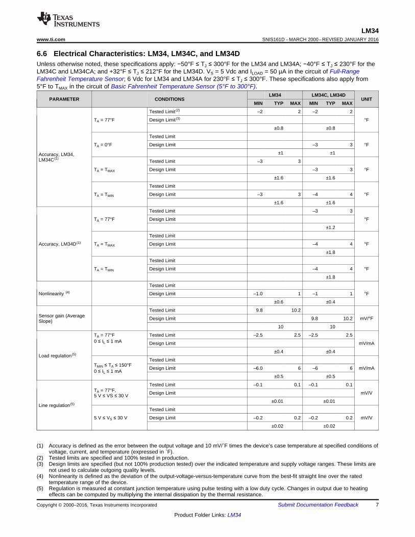
6.6 Electrical Characteristics: LM34, LM34C, and LM34DUnless otherwise noted, these specifications apply: −50°F ≤ TJ ≤ 300°F for the LM34 and LM34A; −40°F ≤ TJ ≤ 230°F for theLM34C and LM34CA; and +32°F ≤ TJ ≤ 212°F for the LM34D. VS = 5 Vdc and ILOAD = 50 µA in the circuit of Full-RangeFahrenheit Temperature Sensor; 6 Vdc for LM34 and LM34A for 230°F ≤ TJ ≤ 300°F. These specifications also apply from5°F to TMAX in the circuit of Basic Fahrenheit Temperature Sensor (5°F to 300°F).
LM34 LM34C, LM34DPARAMETER CONDITIONS UNIT
MIN TYP MAX MIN TYP MAX
Tested Limit (2) –2 2 –2 2
TA = 77°F Design Limit (3) °F
±0.8 ±0.8
Tested Limit
TA = 0°F Design Limit –3 3 °F
±1 ±1Accuracy, LM34,LM34C (1)
Tested Limit –3 3
TA = TMAX Design Limit –3 3 °F
±1.6 ±1.6
Tested Limit
TA = TMIN Design Limit –3 3 –4 4 °F
±1.6 ±1.6
Tested Limit –3 3
TA = 77°F Design Limit °F
±1.2
Tested Limit
Accuracy, LM34D (1) TA = TMAX Design Limit –4 4 °F
±1.8
Tested Limit
TA = TMIN Design Limit –4 4 °F
±1.8
Tested Limit
Nonlinearity (4) Design Limit –1.0 1 –1 1 °F
±0.6 ±0.4
Tested Limit 9.8 10.2Sensor gain (Average Design Limit 9.8 10.2 mV/°FSlope)
10 10
TA = 77°F Tested Limit –2.5 2.5 –2.5 2.50 ≤ IL ≤ 1 mA Design Limit mV/mA
±0.4 ±0.4Load regulation (5)
Tested LimitTMIN ≤ TA ≤ 150°F Design Limit –6.0 6 –6 6 mV/mA0 ≤ IL ≤ 1 mA
±0.5 ±0.5
Tested Limit –0.1 0.1 –0.1 0.1TA = 77°F, Design Limit mV/V5 V ≤ VS ≤ 30 V
±0.01 ±0.01Line regulation (5)
Tested Limit
5 V ≤ VS ≤ 30 V Design Limit –0.2 0.2 –0.2 0.2 mV/V
±0.02 ±0.02
(1) Accuracy is defined as the error between the output voltage and 10 mV/˚F times the device’s case temperature at specified conditions ofvoltage, current, and temperature (expressed in ˚F).
(2) Tested limits are specified and 100% tested in production.(3) Design limits are specified (but not 100% production tested) over the indicated temperature and supply voltage ranges. These limits are
not used to calculate outgoing quality levels.(4) Nonlinearity is defined as the deviation of the output-voltage-versus-temperature curve from the best-fit straight line over the rated
temperature range of the device.(5) Regulation is measured at constant junction temperature using pulse testing with a low duty cycle. Changes in output due to heating
effects can be computed by multiplying the internal dissipation by the thermal resistance.
Copyright © 2000–2016, Texas Instruments Incorporated Submit Documentation Feedback 7
Product Folder Links: LM34
LM34SNIS161D –MARCH 2000–REVISED JANUARY 2016 www.ti.com
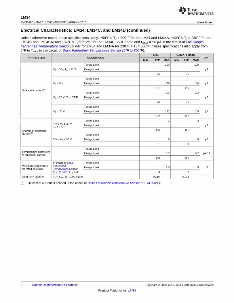
Electrical Characteristics: LM34, LM34C, and LM34D (continued)Unless otherwise noted, these specifications apply: −50°F ≤ TJ ≤ 300°F for the LM34 and LM34A; −40°F ≤ TJ ≤ 230°F for theLM34C and LM34CA; and +32°F ≤ TJ ≤ 212°F for the LM34D. VS = 5 Vdc and ILOAD = 50 µA in the circuit of Full-RangeFahrenheit Temperature Sensor; 6 Vdc for LM34 and LM34A for 230°F ≤ TJ ≤ 300°F. These specifications also apply from5°F to TMAX in the circuit of Basic Fahrenheit Temperature Sensor (5°F to 300°F).
LM34 LM34C, LM34DPARAMETER CONDITIONS UNIT
MIN TYP MAX MIN TYP MAX
Tested Limit 100 100
VS = 5 V, TA = 77°F Design Limit µA
75 75
Tested Limit
VS = 5 V Design Limit 176 154 µA
131 116Quiescent current (6)
Tested Limit 103 103
VS = 30 V, TA = 77°F Design Limit µA
76 76
Tested Limit
VS = 30 V Design Limit 181 159 µA
132 117
Tested Limit 3 34 V ≤ VS ≤ 30 V, Design Limit µATA = +77°F
0.5 0.5Change of quiescentcurrent (5)
Tested Limit
5 V ≤ VS ≤ 30 V Design Limit 5 5 µA
1 1
Tested LimitTemperature coefficient Design Limit 0.7 0.7 µA/°Fof quiescent current
0.3 0.3
Tested LimitIn circuit of BasicMinimum temperature Fahrenheit Design Limit 5.0 5 °Ffor rated accuracy Temperature Sensor
(5°F to 300°F), IL = 0 3 3
Long-term stability TJ = TMAX for 1000 hours ±0.16 ±0.16 °F
(6) Quiescent current is defined in the circuit of Basic Fahrenheit Temperature Sensor (5°F to 300°F).
8 Submit Documentation Feedback Copyright © 2000–2016, Texas Instruments Incorporated
Product Folder Links: LM34
LM34www.ti.com SNIS161D –MARCH 2000–REVISED JANUARY 2016
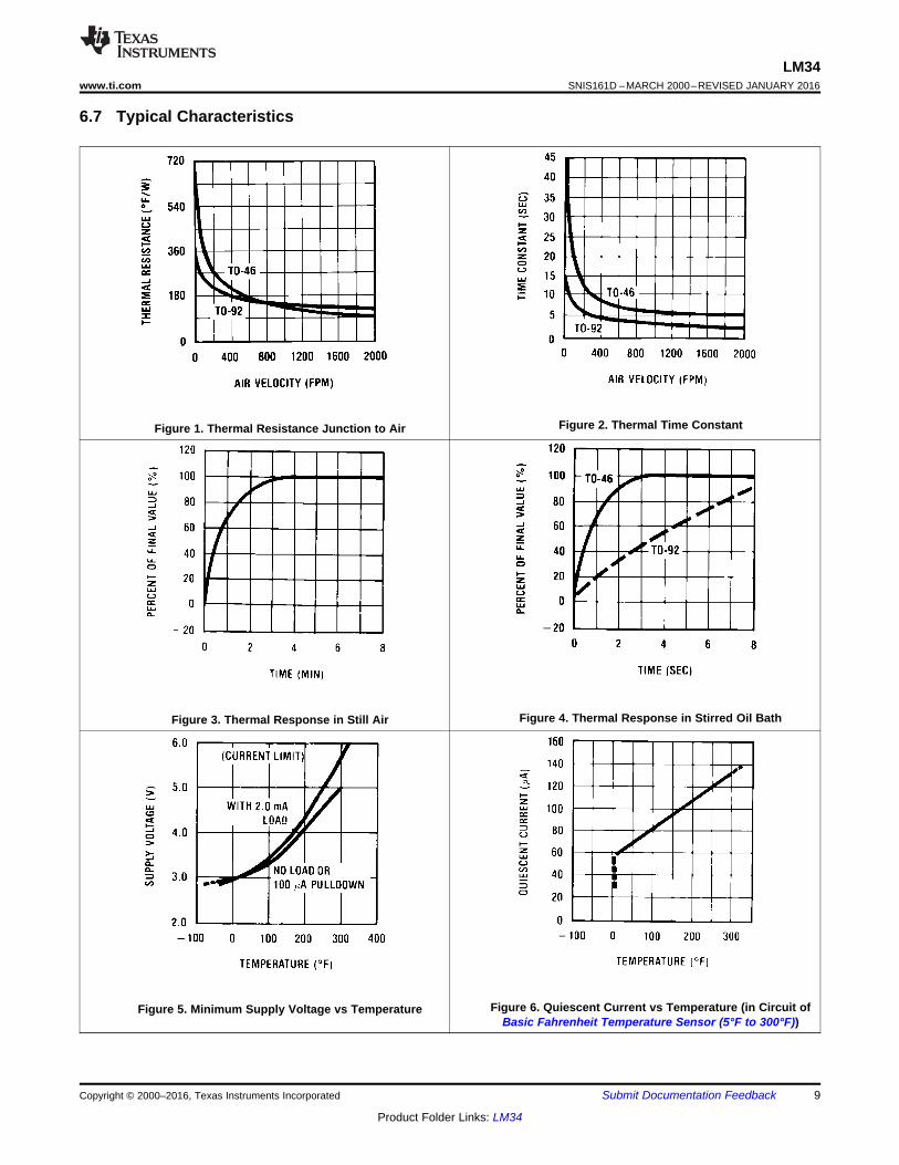
6.7 Typical Characteristics
Figure 2. Thermal Time ConstantFigure 1. Thermal Resistance Junction to Air
Figure 4. Thermal Response in Stirred Oil BathFigure 3. Thermal Response in Still Air
Figure 6. Quiescent Current vs Temperature (in Circuit ofFigure 5. Minimum Supply Voltage vs TemperatureBasic Fahrenheit Temperature Sensor (5°F to 300°F))
Copyright © 2000–2016, Texas Instruments Incorporated Submit Documentation Feedback 9
Product Folder Links: LM34
LM34SNIS161D –MARCH 2000–REVISED JANUARY 2016 www.ti.com
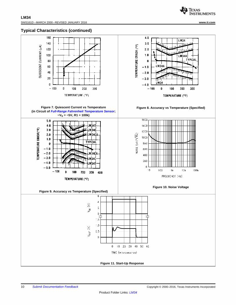
Typical Characteristics (continued)
Figure 7. Quiescent Current vs Temperature Figure 8. Accuracy vs Temperature (Specified)(in Circuit of Full-Range Fahrenheit Temperature Sensor;
−VS = −5V, R1 = 100k)
Figure 10. Noise VoltageFigure 9. Accuracy vs Temperature (Specified)
Figure 11. Start-Up Response
10 Submit Documentation Feedback Copyright © 2000–2016, Texas Instruments Incorporated
Product Folder Links: LM34
LM34www.ti.com SNIS161D –MARCH 2000–REVISED JANUARY 2016
7 Detailed Description
7.1 OverviewThe LM34 series devices are precision integrated-circuit temperature sensors, whose output voltage is linearlyproportional to the Fahrenheit temperature. The LM34 device has an advantage over linear temperature sensorscalibrated in degrees Kelvin, because the user is not required to subtract a large constant voltage from its outputto obtain convenient Fahrenheit scaling. The LM34 device does not require any external calibration or trimmingto provide typical accuracies of ±1/2°F at room temperature and ±1-1⁄2°F over a full −50°F to 300°F temperaturerange. Lower cost is assured by trimming and calibration at the wafer level. The low output impedance, linearoutput, and precise inherent calibration of the LM34 device makes interfacing to readout or control circuitryespecially easy. It can be used with single power supplies or with plus and minus supplies. Because the LM34device draws only 75 µA from its supply, the device has very low self-heating, less than 0.2°F in still air.
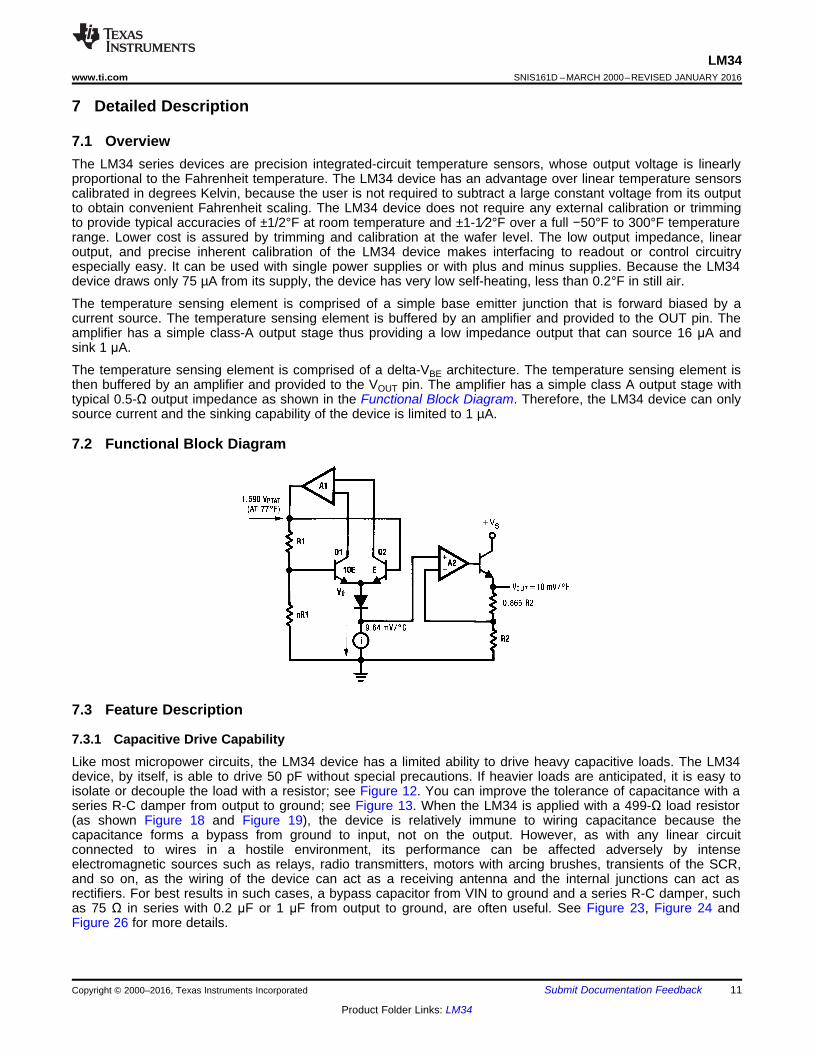
The temperature sensing element is comprised of a simple base emitter junction that is forward biased by acurrent source. The temperature sensing element is buffered by an amplifier and provided to the OUT pin. Theamplifier has a simple class-A output stage thus providing a low impedance output that can source 16 μA andsink 1 μA.
The temperature sensing element is comprised of a delta-VBE architecture. The temperature sensing element isthen buffered by an amplifier and provided to the VOUT pin. The amplifier has a simple class A output stage withtypical 0.5-Ω output impedance as shown in the Functional Block Diagram. Therefore, the LM34 device can onlysource current and the sinking capability of the device is limited to 1 µA.
7.2 Functional Block Diagram
7.3 Feature Description
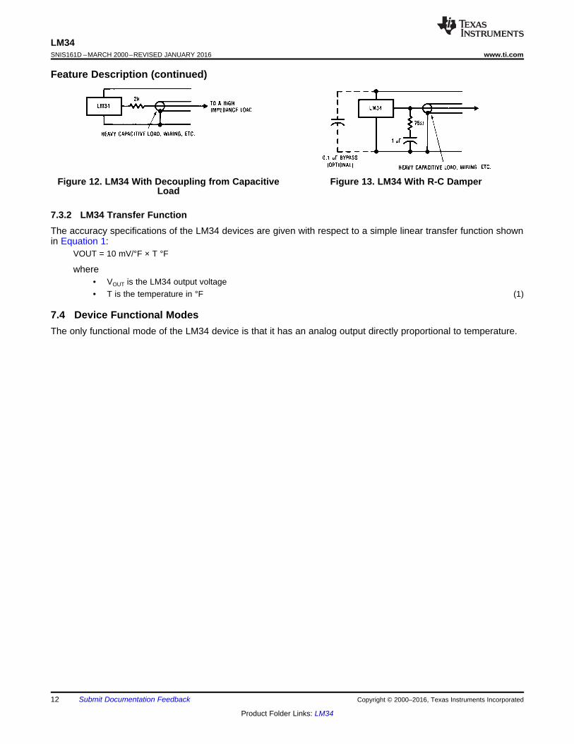
7.3.1 Capacitive Drive CapabilityLike most micropower circuits, the LM34 device has a limited ability to drive heavy capacitive loads. The LM34device, by itself, is able to drive 50 pF without special precautions. If heavier loads are anticipated, it is easy toisolate or decouple the load with a resistor; see Figure 12. You can improve the tolerance of capacitance with aseries R-C damper from output to ground; see Figure 13. When the LM34 is applied with a 499-Ω load resistor(as shown Figure 18 and Figure 19), the device is relatively immune to wiring capacitance because thecapacitance forms a bypass from ground to input, not on the output. However, as with any linear circuitconnected to wires in a hostile environment, its performance can be affected adversely by intenseelectromagnetic sources such as relays, radio transmitters, motors with arcing brushes, transients of the SCR,and so on, as the wiring of the device can act as a receiving antenna and the internal junctions can act asrectifiers. For best results in such cases, a bypass capacitor from VIN to ground and a series R-C damper, suchas 75 Ω in series with 0.2 μF or 1 μF from output to ground, are often useful. See Figure 23, Figure 24 andFigure 26 for more details.
Copyright © 2000–2016, Texas Instruments Incorporated Submit Documentation Feedback 11
Product Folder Links: LM34
LM34SNIS161D –MARCH 2000–REVISED JANUARY 2016 www.ti.com
Feature Description (continued)
Figure 12. LM34 With Decoupling from Capacitive Figure 13. LM34 With R-C DamperLoad
7.3.2 LM34 Transfer FunctionThe accuracy specifications of the LM34 devices are given with respect to a simple linear transfer function shownin Equation 1:
VOUT = 10 mV/°F × T °F
where• VOUT is the LM34 output voltage• T is the temperature in °F (1)
7.4 Device Functional ModesThe only functional mode of the LM34 device is that it has an analog output directly proportional to temperature.
12 Submit Documentation Feedback Copyright © 2000–2016, Texas Instruments Incorporated
Product Folder Links: LM34
LM34www.ti.com SNIS161D –MARCH 2000–REVISED JANUARY 2016
8 Application and Implementation
NOTEInformation in the following applications sections is not part of the TI componentspecification, and TI does not warrant its accuracy or completeness. TI’s customers areresponsible for determining suitability of components for their purposes. Customers shouldvalidate and test their design implementation to confirm system functionality.
8.1 Application InformationThe features of the LM34 device make it suitable for many general temperature sensing applications. Multiplepackage options expand on flexibility of the device.
8.2 Typical Application
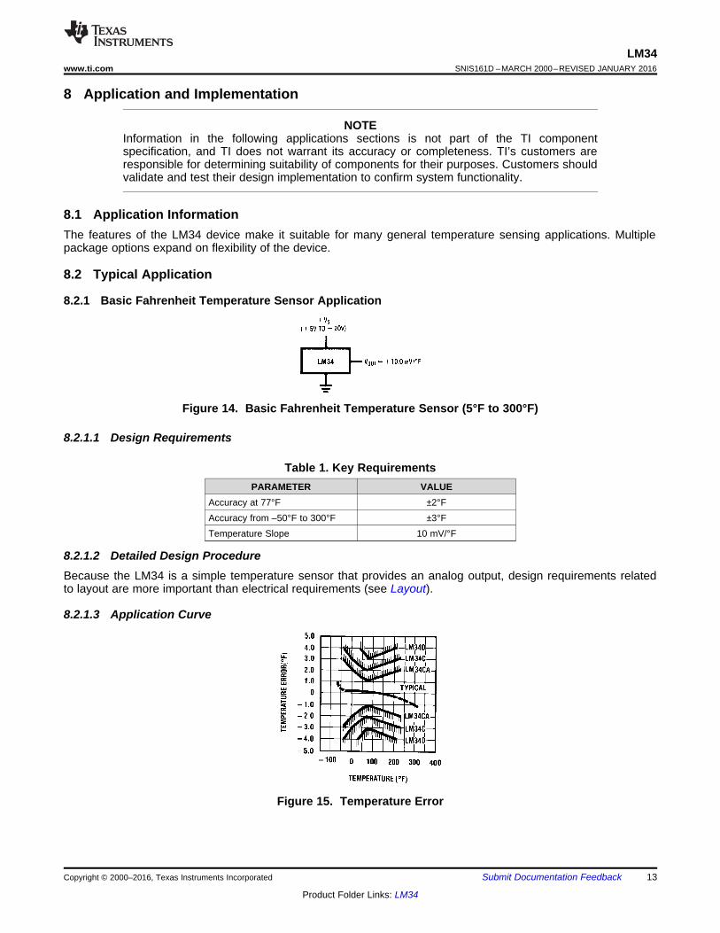
8.2.1 Basic Fahrenheit Temperature Sensor Application
Figure 14. Basic Fahrenheit Temperature Sensor (5°F to 300°F)
8.2.1.1 Design Requirements
Table 1. Key RequirementsPARAMETER VALUE
Accuracy at 77°F ±2°FAccuracy from –50°F to 300°F ±3°FTemperature Slope 10 mV/°F
8.2.1.2 Detailed Design ProcedureBecause the LM34 is a simple temperature sensor that provides an analog output, design requirements relatedto layout are more important than electrical requirements (see Layout).
8.2.1.3 Application Curve
Figure 15. Temperature Error
Copyright © 2000–2016, Texas Instruments Incorporated Submit Documentation Feedback 13
Product Folder Links: LM34
LM34SNIS161D –MARCH 2000–REVISED JANUARY 2016 www.ti.com
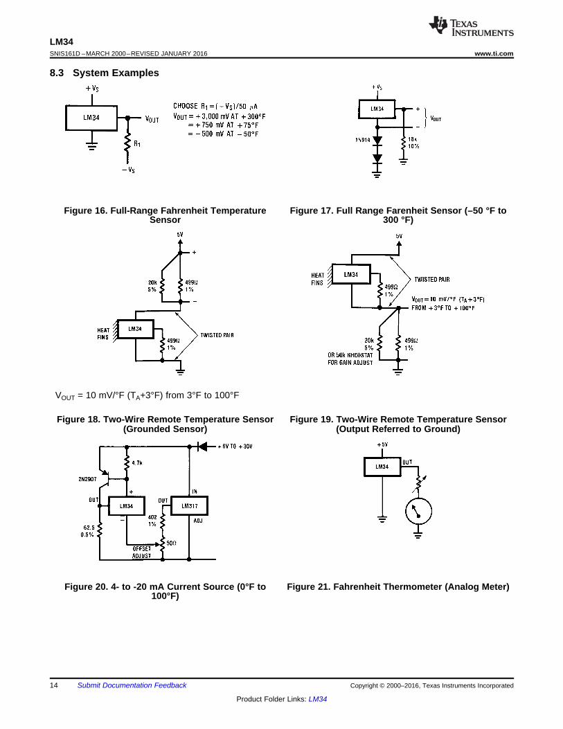
8.3 System Examples
Figure 16. Full-Range Fahrenheit Temperature Figure 17. Full Range Farenheit Sensor (–50 °F toSensor 300 °F)
VOUT = 10 mV/°F (TA+3°F) from 3°F to 100°F
Figure 18. Two-Wire Remote Temperature Sensor Figure 19. Two-Wire Remote Temperature Sensor(Grounded Sensor) (Output Referred to Ground)
Figure 20. 4- to -20 mA Current Source (0°F to Figure 21. Fahrenheit Thermometer (Analog Meter)100°F)
14 Submit Documentation Feedback Copyright © 2000–2016, Texas Instruments Incorporated
Product Folder Links: LM34
∗ = 1% or 2% film resistor
— Trim R for V = 3.525VB B
— Trim R for V = 2.725VC C
— Trim R for V = 0.085V + 40 mV/°F x T
— Example, V = 3.285V at 80°FA A AMBIENT
A
LM34www.ti.com SNIS161D –MARCH 2000–REVISED JANUARY 2016
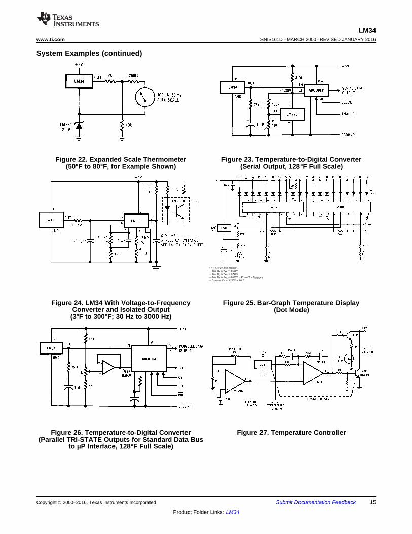
System Examples (continued)
Figure 22. Expanded Scale Thermometer Figure 23. Temperature-to-Digital Converter(50°F to 80°F, for Example Shown) (Serial Output, 128°F Full Scale)
Figure 24. LM34 With Voltage-to-Frequency Figure 25. Bar-Graph Temperature DisplayConverter and Isolated Output (Dot Mode)
(3°F to 300°F; 30 Hz to 3000 Hz)
Figure 26. Temperature-to-Digital Converter Figure 27. Temperature Controller(Parallel TRI-STATE Outputs for Standard Data Bus
to µP Interface, 128°F Full Scale)
Copyright © 2000–2016, Texas Instruments Incorporated Submit Documentation Feedback 15
Product Folder Links: LM34
LM34SNIS161D –MARCH 2000–REVISED JANUARY 2016 www.ti.com
9 Power Supply RecommendationsIt may be necessary to add a bypass filter capacitor in noisy environments, as shown in as shown in Figure 13.
10 Layout
10.1 Layout GuidelinesThe LM34 device can be easily applied in the same way as other integrated-circuit temperature sensors. Thedevice can be glued or cemented to a surface and its temperature will be within about 0.02°F of the surfacetemperature. This presumes that the ambient air temperature is almost the same as the surface temperature; ifthe air temperature were much higher or lower than the surface temperature, the actual temperature of the LM34die would be at an intermediate temperature between the surface temperature and the air temperature. This isespecially true for the TO-92 plastic package, where the copper leads are the principal thermal path to carry heatinto the device, so its temperature might be closer to the air temperature than to the surface temperature.
To minimize this problem, be sure that the wiring to the LM34, as it leaves the device, is held at the sametemperature as the surface of interest. The easiest way to do this is to cover up these wires with a bead ofepoxy, which will insure that the leads and wires are all at the same temperature as the surface, and that the dietemperature of the LM34 device will not be affected by the air temperature.
The TO-46 metal package can be soldered to a metal surface or pipe without damage. In the case wheresoldering is used, the V− terminal of the circuit will be grounded to that metal. Alternatively, the LM34 device canbe mounted inside a sealed-end metal tube, and can then be dipped into a bath or screwed into a threaded holein a tank. As with any IC, the LM34 and accompanying wiring and circuits must be kept insulated and dry, toavoid leakage and corrosion. This is especially true if the circuit may operate at cold temperatures wherecondensation can occur. Printed-circuit coatings and varnishes such as a conformal coating and epoxy paints ordips are often used to insure that moisture cannot corrode the LM34 or its connections.
These devices are sometimes soldered to a small, light-weight heat fin to decrease the thermal time constantand speed up the response in slowly-moving air. On the other hand, a small thermal mass may be added to thesensor to give the steadiest reading despite small deviations in the air temperature.
Table 2. Temperature Rise of LM34 Due to Self-Heating (Thermal Resistance)TO-46, TO-92,TO-46 TO-92, SO-8 SO-8CONDITIONS SMALL HEAT SMALL HEATNO HEAT SINK NO HEAT SINK NO HEAT SINK SMALL HEAT FinFin (1) Fin (2)
Still air 720°F/W 180°F/W 324°F/W 252°F/W 400°F/W 200°F/WMoving air 180°F/W 72°F/W 162°F/W 126°F/W 190°F/W 160°F/WStill oil 180°F/W 72°F/W 162°F/W 126°F/W — —Stirred oil 90°F/W 54°F/W 81°F/W 72°F/W — —(Clamped to metal, (43°F/W ) — — (95°F/W )infinite heart sink)
(1) Wakefield type 201 or 1-inch disc of 0.020-inch sheet brass, soldered to case, or similar.(2) TO-92 and SO-8 packages glued and leads soldered to 1-inch square of 1/16 inches printed circuit board with 2 oz copper foil, or
similar.
16 Submit Documentation Feedback Copyright © 2000–2016, Texas Instruments Incorporated
Product Folder Links: LM34
VOUT
N.C.
N.C.
+VS
N.C.
0.01µ F
VIA to ground plane
VIA to power plane
GND N.C.
N.C.
LM34www.ti.com SNIS161D –MARCH 2000–REVISED JANUARY 2016
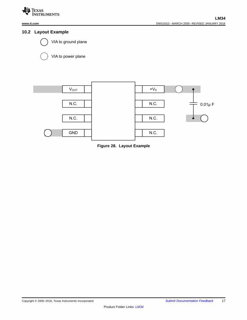
10.2 Layout Example
Figure 28. Layout Example
Copyright © 2000–2016, Texas Instruments Incorporated Submit Documentation Feedback 17
Product Folder Links: LM34
LM34SNIS161D –MARCH 2000–REVISED JANUARY 2016 www.ti.com
11 Device and Documentation Support
11.1 TrademarksAll trademarks are the property of their respective owners.
11.2 Electrostatic Discharge CautionThese devices have limited built-in ESD protection. The leads should be shorted together or the device placed in conductive foamduring storage or handling to prevent electrostatic damage to the MOS gates.
11.3 GlossarySLYZ022 — TI Glossary.
This glossary lists and explains terms, acronyms, and definitions.
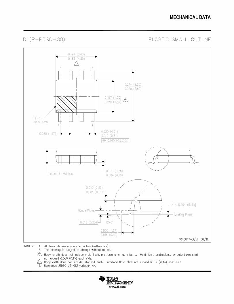
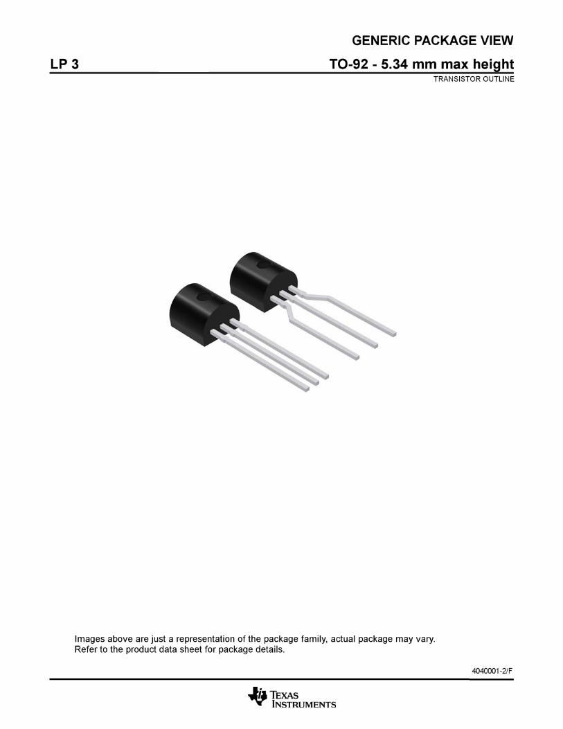
12 Mechanical, Packaging, and Orderable InformationThe following pages include mechanical, packaging, and orderable information. This information is the mostcurrent data available for the designated devices. This data is subject to change without notice and revision ofthis document. For browser-based versions of this data sheet, refer to the left-hand navigation.
18 Submit Documentation Feedback Copyright © 2000–2016, Texas Instruments Incorporated
Product Folder Links: LM34
PACKAGE OPTION ADDENDUM
www.ti.com 17-Mar-2017
Addendum-Page 1
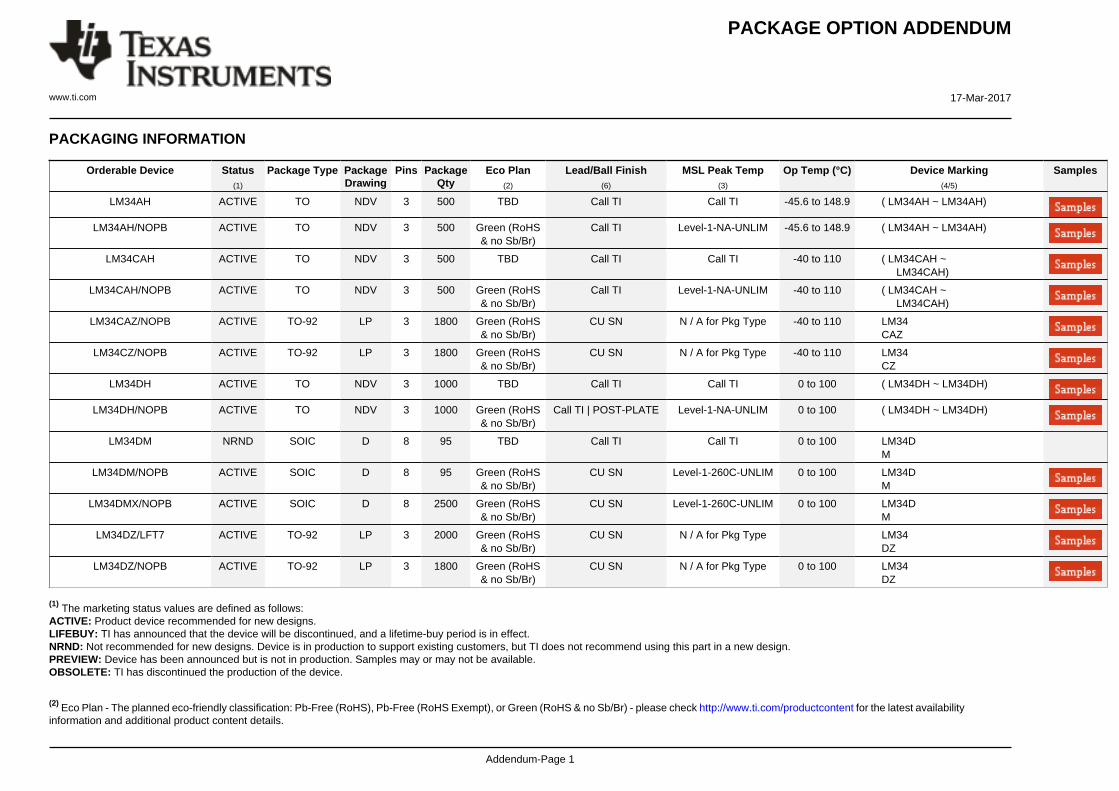
PACKAGING INFORMATION
Orderable Device Status(1)
Package Type PackageDrawing
Pins PackageQty
Eco Plan(2)
Lead/Ball Finish(6)
MSL Peak Temp(3)
Op Temp (°C) Device Marking(4/5)
Samples
LM34AH ACTIVE TO NDV 3 500 TBD Call TI Call TI -45.6 to 148.9 ( LM34AH ~ LM34AH)
LM34AH/NOPB ACTIVE TO NDV 3 500 Green (RoHS& no Sb/Br)
Call TI Level-1-NA-UNLIM -45.6 to 148.9 ( LM34AH ~ LM34AH)
LM34CAH ACTIVE TO NDV 3 500 TBD Call TI Call TI -40 to 110 ( LM34CAH ~ LM34CAH)
LM34CAH/NOPB ACTIVE TO NDV 3 500 Green (RoHS& no Sb/Br)
Call TI Level-1-NA-UNLIM -40 to 110 ( LM34CAH ~ LM34CAH)
LM34CAZ/NOPB ACTIVE TO-92 LP 3 1800 Green (RoHS& no Sb/Br)
CU SN N / A for Pkg Type -40 to 110 LM34CAZ
LM34CZ/NOPB ACTIVE TO-92 LP 3 1800 Green (RoHS& no Sb/Br)
CU SN N / A for Pkg Type -40 to 110 LM34CZ
LM34DH ACTIVE TO NDV 3 1000 TBD Call TI Call TI 0 to 100 ( LM34DH ~ LM34DH)
LM34DH/NOPB ACTIVE TO NDV 3 1000 Green (RoHS& no Sb/Br)
Call TI | POST-PLATE Level-1-NA-UNLIM 0 to 100 ( LM34DH ~ LM34DH)
LM34DM NRND SOIC D 8 95 TBD Call TI Call TI 0 to 100 LM34DM
LM34DM/NOPB ACTIVE SOIC D 8 95 Green (RoHS& no Sb/Br)
CU SN Level-1-260C-UNLIM 0 to 100 LM34DM
LM34DMX/NOPB ACTIVE SOIC D 8 2500 Green (RoHS& no Sb/Br)
CU SN Level-1-260C-UNLIM 0 to 100 LM34DM
LM34DZ/LFT7 ACTIVE TO-92 LP 3 2000 Green (RoHS& no Sb/Br)
CU SN N / A for Pkg Type LM34DZ
LM34DZ/NOPB ACTIVE TO-92 LP 3 1800 Green (RoHS& no Sb/Br)
CU SN N / A for Pkg Type 0 to 100 LM34DZ
(1) The marketing status values are defined as follows:ACTIVE: Product device recommended for new designs.LIFEBUY: TI has announced that the device will be discontinued, and a lifetime-buy period is in effect.NRND: Not recommended for new designs. Device is in production to support existing customers, but TI does not recommend using this part in a new design.PREVIEW: Device has been announced but is not in production. Samples may or may not be available.OBSOLETE: TI has discontinued the production of the device.
(2) Eco Plan - The planned eco-friendly classification: Pb-Free (RoHS), Pb-Free (RoHS Exempt), or Green (RoHS & no Sb/Br) - please check http://www.ti.com/productcontent for the latest availabilityinformation and additional product content details.
PACKAGE OPTION ADDENDUM
www.ti.com 17-Mar-2017
Addendum-Page 2
TBD: The Pb-Free/Green conversion plan has not been defined.Pb-Free (RoHS): TI's terms "Lead-Free" or "Pb-Free" mean semiconductor products that are compatible with the current RoHS requirements for all 6 substances, including the requirement thatlead not exceed 0.1% by weight in homogeneous materials. Where designed to be soldered at high temperatures, TI Pb-Free products are suitable for use in specified lead-free processes.Pb-Free (RoHS Exempt): This component has a RoHS exemption for either 1) lead-based flip-chip solder bumps used between the die and package, or 2) lead-based die adhesive used betweenthe die and leadframe. The component is otherwise considered Pb-Free (RoHS compatible) as defined above.Green (RoHS & no Sb/Br): TI defines "Green" to mean Pb-Free (RoHS compatible), and free of Bromine (Br) and Antimony (Sb) based flame retardants (Br or Sb do not exceed 0.1% by weightin homogeneous material)
(3) MSL, Peak Temp. - The Moisture Sensitivity Level rating according to the JEDEC industry standard classifications, and peak solder temperature.
(4) There may be additional marking, which relates to the logo, the lot trace code information, or the environmental category on the device.
(5) Multiple Device Markings will be inside parentheses. Only one Device Marking contained in parentheses and separated by a "~" will appear on a device. If a line is indented then it is a continuationof the previous line and the two combined represent the entire Device Marking for that device.
(6) Lead/Ball Finish - Orderable Devices may have multiple material finish options. Finish options are separated by a vertical ruled line. Lead/Ball Finish values may wrap to two lines if the finishvalue exceeds the maximum column width.
Important Information and Disclaimer:The information provided on this page represents TI's knowledge and belief as of the date that it is provided. TI bases its knowledge and belief on informationprovided by third parties, and makes no representation or warranty as to the accuracy of such information. Efforts are underway to better integrate information from third parties. TI has taken andcontinues to take reasonable steps to provide representative and accurate information but may not have conducted destructive testing or chemical analysis on incoming materials and chemicals.TI and TI suppliers consider certain information to be proprietary, and thus CAS numbers and other limited information may not be available for release.
In no event shall TI's liability arising out of such information exceed the total purchase price of the TI part(s) at issue in this document sold by TI to Customer on an annual basis.
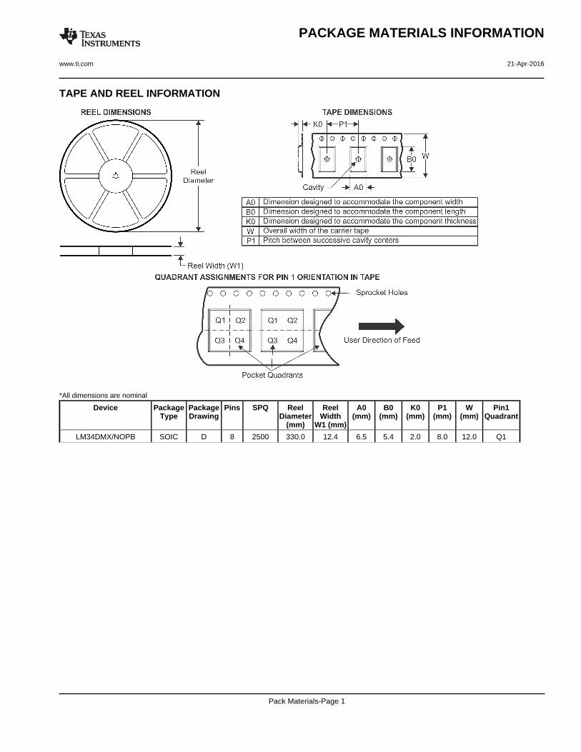
TAPE AND REEL INFORMATION
*All dimensions are nominal
Device PackageType
PackageDrawing
Pins SPQ ReelDiameter
(mm)
ReelWidth
W1 (mm)
A0(mm)
B0(mm)
K0(mm)
P1(mm)
W(mm)
Pin1Quadrant
LM34DMX/NOPB SOIC D 8 2500 330.0 12.4 6.5 5.4 2.0 8.0 12.0 Q1
PACKAGE MATERIALS INFORMATION
www.ti.com 21-Apr-2016
Pack Materials-Page 1
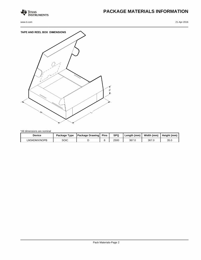
*All dimensions are nominal
Device Package Type Package Drawing Pins SPQ Length (mm) Width (mm) Height (mm)
LM34DMX/NOPB SOIC D 8 2500 367.0 367.0 35.0
PACKAGE MATERIALS INFORMATION
www.ti.com 21-Apr-2016
Pack Materials-Page 2
www.ti.com
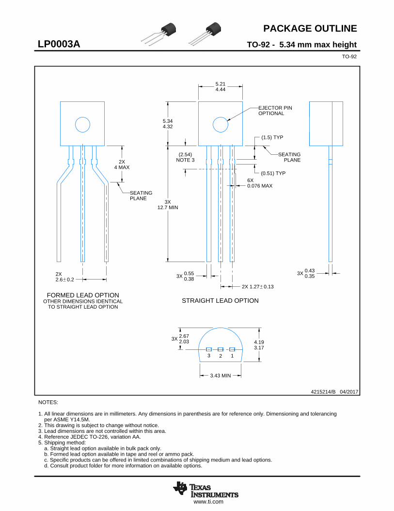
PACKAGE OUTLINE
3X 2.672.03
5.214.44
5.344.32
3X12.7 MIN
2X 1.27 0.13
3X 0.550.38
4.193.17
3.43 MIN
3X 0.430.35
(2.54)NOTE 3
2X2.6 0.2
2X4 MAX
SEATINGPLANE
6X0.076 MAX
(0.51) TYP
(1.5) TYP
TO-92 - 5.34 mm max heightLP0003ATO-92
4215214/B 04/2017
NOTES: 1. All linear dimensions are in millimeters. Any dimensions in parenthesis are for reference only. Dimensioning and tolerancing per ASME Y14.5M.2. This drawing is subject to change without notice.3. Lead dimensions are not controlled within this area.4. Reference JEDEC TO-226, variation AA.5. Shipping method: a. Straight lead option available in bulk pack only. b. Formed lead option available in tape and reel or ammo pack. c. Specific products can be offered in limited combinations of shipping medium and lead options. d. Consult product folder for more information on available options.
EJECTOR PINOPTIONAL
PLANESEATING
STRAIGHT LEAD OPTION
3 2 1
SCALE 1.200
FORMED LEAD OPTIONOTHER DIMENSIONS IDENTICAL
TO STRAIGHT LEAD OPTION
SCALE 1.200

www.ti.com
EXAMPLE BOARD LAYOUT
0.05 MAXALL AROUND
TYP
(1.07)
(1.5) 2X (1.5)
2X (1.07)(1.27)
(2.54)
FULL RTYP
( 1.4)0.05 MAXALL AROUND
TYP
(2.6)
(5.2)
(R0.05) TYP
3X ( 0.9) HOLE
2X ( 1.4)METAL
3X ( 0.85) HOLE
(R0.05) TYP
4215214/B 04/2017
TO-92 - 5.34 mm max heightLP0003ATO-92
LAND PATTERN EXAMPLEFORMED LEAD OPTIONNON-SOLDER MASK DEFINED
SCALE:15X
SOLDER MASKOPENING
METAL
2XSOLDER MASKOPENING
1 2 3
LAND PATTERN EXAMPLESTRAIGHT LEAD OPTIONNON-SOLDER MASK DEFINED
SCALE:15X
METALTYP
SOLDER MASKOPENING
2XSOLDER MASKOPENING
2XMETAL
1 2 3
www.ti.com
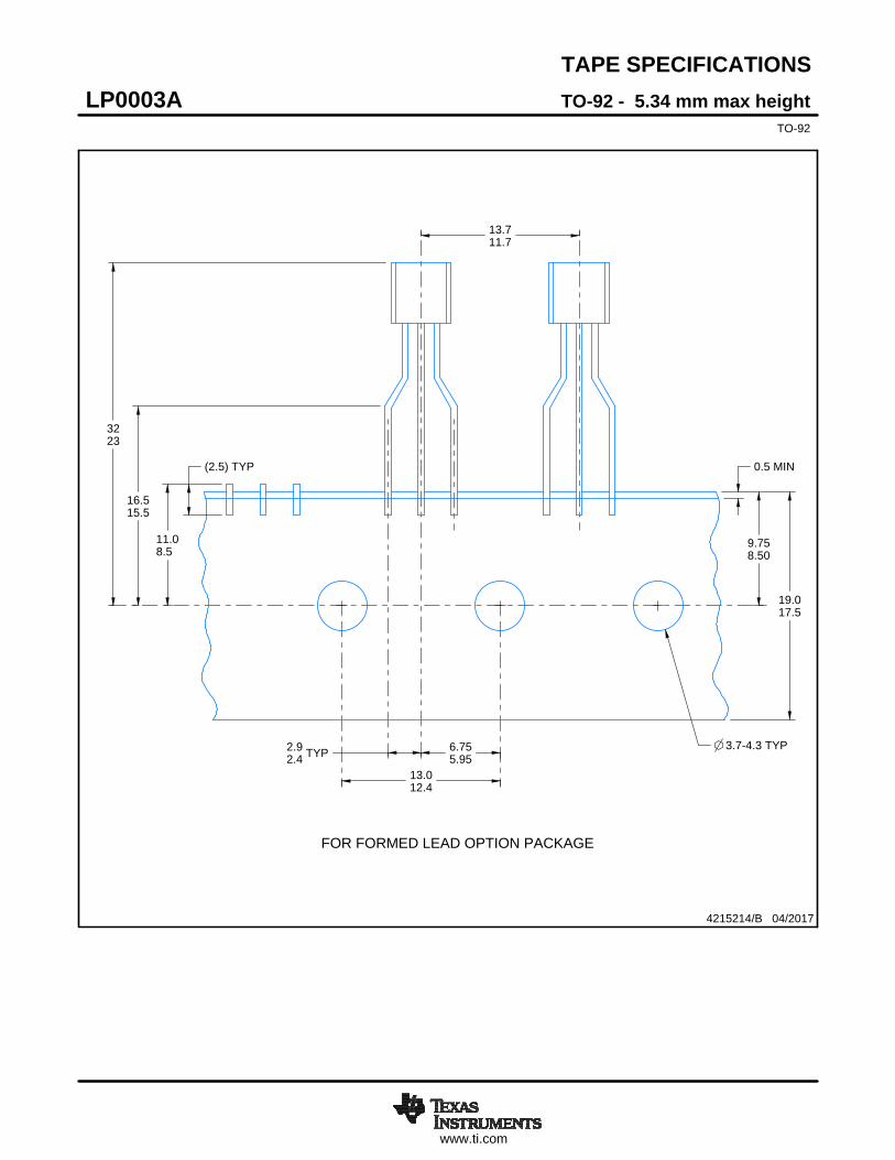
TAPE SPECIFICATIONS
19.017.5
13.711.7
11.08.5
0.5 MIN
TYP-4.33.7
9.758.50
TYP2.92.4
6.755.95
13.012.4
(2.5) TYP
16.515.5
3223
4215214/B 04/2017
TO-92 - 5.34 mm max heightLP0003ATO-92
FOR FORMED LEAD OPTION PACKAGE
www.ti.com
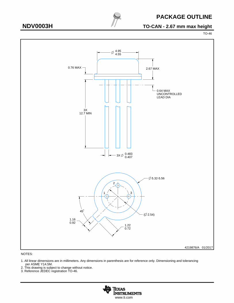
PACKAGE OUTLINE
( 2.54)1.160.92
4.954.55
0.76 MAX 2.67 MAX
0.64 MAXUNCONTROLLEDLEAD DIA
3X12.7 MIN
3X 0.4830.407
-5.565.32
1.220.72
45
TO-CAN - 2.67 mm max heightNDV0003HTO-46
4219876/A 01/2017
NOTES: 1. All linear dimensions are in millimeters. Any dimensions in parenthesis are for reference only. Dimensioning and tolerancing per ASME Y14.5M.2. This drawing is subject to change without notice.3. Reference JEDEC registration TO-46.
1
2
3
SCALE 1.250
www.ti.com
EXAMPLE BOARD LAYOUT
0.07 MAXALL AROUND
0.07 MAXTYP
( 1.2)METAL
2X ( 1.2) METAL
3X ( 0.7) VIA
(R0.05) TYP
(2.54)
(1.27)
TO-CAN - 2.67 mm max heightNDV0003HTO-46
4219876/A 01/2017
LAND PATTERN EXAMPLENON-SOLDER MASK DEFINED
SCALE:12X
2XSOLDER MASKOPENING
SOLDER MASKOPENING
1
2
3
IMPORTANT NOTICE
Texas Instruments Incorporated (TI) reserves the right to make corrections, enhancements, improvements and other changes to itssemiconductor products and services per JESD46, latest issue, and to discontinue any product or service per JESD48, latest issue. Buyersshould obtain the latest relevant information before placing orders and should verify that such information is current and complete.TI’s published terms of sale for semiconductor products (http://www.ti.com/sc/docs/stdterms.htm) apply to the sale of packaged integratedcircuit products that TI has qualified and released to market. Additional terms may apply to the use or sale of other types of TI products andservices.Reproduction of significant portions of TI information in TI data sheets is permissible only if reproduction is without alteration and isaccompanied by all associated warranties, conditions, limitations, and notices. TI is not responsible or liable for such reproduceddocumentation. Information of third parties may be subject to additional restrictions. Resale of TI products or services with statementsdifferent from or beyond the parameters stated by TI for that product or service voids all express and any implied warranties for theassociated TI product or service and is an unfair and deceptive business practice. TI is not responsible or liable for any such statements.Buyers and others who are developing systems that incorporate TI products (collectively, “Designers”) understand and agree that Designersremain responsible for using their independent analysis, evaluation and judgment in designing their applications and that Designers havefull and exclusive responsibility to assure the safety of Designers' applications and compliance of their applications (and of all TI productsused in or for Designers’ applications) with all applicable regulations, laws and other applicable requirements. Designer represents that, withrespect to their applications, Designer has all the necessary expertise to create and implement safeguards that (1) anticipate dangerousconsequences of failures, (2) monitor failures and their consequences, and (3) lessen the likelihood of failures that might cause harm andtake appropriate actions. Designer agrees that prior to using or distributing any applications that include TI products, Designer willthoroughly test such applications and the functionality of such TI products as used in such applications.TI’s provision of technical, application or other design advice, quality characterization, reliability data or other services or information,including, but not limited to, reference designs and materials relating to evaluation modules, (collectively, “TI Resources”) are intended toassist designers who are developing applications that incorporate TI products; by downloading, accessing or using TI Resources in anyway, Designer (individually or, if Designer is acting on behalf of a company, Designer’s company) agrees to use any particular TI Resourcesolely for this purpose and subject to the terms of this Notice.TI’s provision of TI Resources does not expand or otherwise alter TI’s applicable published warranties or warranty disclaimers for TIproducts, and no additional obligations or liabilities arise from TI providing such TI Resources. TI reserves the right to make corrections,enhancements, improvements and other changes to its TI Resources. TI has not conducted any testing other than that specificallydescribed in the published documentation for a particular TI Resource.Designer is authorized to use, copy and modify any individual TI Resource only in connection with the development of applications thatinclude the TI product(s) identified in such TI Resource. NO OTHER LICENSE, EXPRESS OR IMPLIED, BY ESTOPPEL OR OTHERWISETO ANY OTHER TI INTELLECTUAL PROPERTY RIGHT, AND NO LICENSE TO ANY TECHNOLOGY OR INTELLECTUAL PROPERTYRIGHT OF TI OR ANY THIRD PARTY IS GRANTED HEREIN, including but not limited to any patent right, copyright, mask work right, orother intellectual property right relating to any combination, machine, or process in which TI products or services are used. Informationregarding or referencing third-party products or services does not constitute a license to use such products or services, or a warranty orendorsement thereof. Use of TI Resources may require a license from a third party under the patents or other intellectual property of thethird party, or a license from TI under the patents or other intellectual property of TI.TI RESOURCES ARE PROVIDED “AS IS” AND WITH ALL FAULTS. TI DISCLAIMS ALL OTHER WARRANTIES ORREPRESENTATIONS, EXPRESS OR IMPLIED, REGARDING RESOURCES OR USE THEREOF, INCLUDING BUT NOT LIMITED TOACCURACY OR COMPLETENESS, TITLE, ANY EPIDEMIC FAILURE WARRANTY AND ANY IMPLIED WARRANTIES OFMERCHANTABILITY, FITNESS FOR A PARTICULAR PURPOSE, AND NON-INFRINGEMENT OF ANY THIRD PARTY INTELLECTUALPROPERTY RIGHTS. TI SHALL NOT BE LIABLE FOR AND SHALL NOT DEFEND OR INDEMNIFY DESIGNER AGAINST ANY CLAIM,INCLUDING BUT NOT LIMITED TO ANY INFRINGEMENT CLAIM THAT RELATES TO OR IS BASED ON ANY COMBINATION OFPRODUCTS EVEN IF DESCRIBED IN TI RESOURCES OR OTHERWISE. IN NO EVENT SHALL TI BE LIABLE FOR ANY ACTUAL,DIRECT, SPECIAL, COLLATERAL, INDIRECT, PUNITIVE, INCIDENTAL, CONSEQUENTIAL OR EXEMPLARY DAMAGES INCONNECTION WITH OR ARISING OUT OF TI RESOURCES OR USE THEREOF, AND REGARDLESS OF WHETHER TI HAS BEENADVISED OF THE POSSIBILITY OF SUCH DAMAGES.Unless TI has explicitly designated an individual product as meeting the requirements of a particular industry standard (e.g., ISO/TS 16949and ISO 26262), TI is not responsible for any failure to meet such industry standard requirements.Where TI specifically promotes products as facilitating functional safety or as compliant with industry functional safety standards, suchproducts are intended to help enable customers to design and create their own applications that meet applicable functional safety standardsand requirements. Using products in an application does not by itself establish any safety features in the application. Designers mustensure compliance with safety-related requirements and standards applicable to their applications. Designer may not use any TI products inlife-critical medical equipment unless authorized officers of the parties have executed a special contract specifically governing such use.Life-critical medical equipment is medical equipment where failure of such equipment would cause serious bodily injury or death (e.g., lifesupport, pacemakers, defibrillators, heart pumps, neurostimulators, and implantables). Such equipment includes, without limitation, allmedical devices identified by the U.S. Food and Drug Administration as Class III devices and equivalent classifications outside the U.S.TI may expressly designate certain products as completing a particular qualification (e.g., Q100, Military Grade, or Enhanced Product).Designers agree that it has the necessary expertise to select the product with the appropriate qualification designation for their applicationsand that proper product selection is at Designers’ own risk. Designers are solely responsible for compliance with all legal and regulatoryrequirements in connection with such selection.Designer will fully indemnify TI and its representatives against any damages, costs, losses, and/or liabilities arising out of Designer’s non-compliance with the terms and provisions of this Notice.
Mailing Address: Texas Instruments, Post Office Box 655303, Dallas, Texas 75265Copyright © 2017, Texas Instruments Incorporated