Lecture-3 Microwave Engineering Instructor: Athar Hanif.
28
Lecture-3 Microwave Engineering Instructor: Athar Hanif
-
Upload
leslie-lester -
Category
Documents
-
view
247 -
download
2
Transcript of Lecture-3 Microwave Engineering Instructor: Athar Hanif.

Lecture-3
Microwave Engineering
Instructor: Athar Hanif

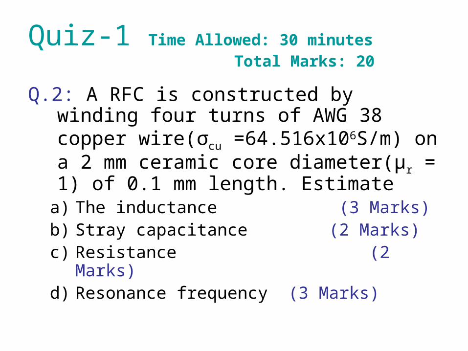
Quiz-1 Time Allowed: 30 minutes Total Marks: 20
Q.1:A plane wave traveling in z- direction in a dielectric medium with єr =2.55 has an electric field given by Ey = E0 cos(ωt-βz). The frequency is 2.4 GHz, and E0 = 30 V/m.
a) Find the amplitude and direction of the magnetic field. (2 Marks)
b) Find the phase velocity and wavelength. (3 Marks)
a) Find the phase shift between the positions Z1 = 0.5 m and Z2 = 1.7 m. (5 Marks)
Quiz-1 Time Allowed: 30 minutes Total Marks: 20
Q.2: A RFC is constructed by winding four turns of AWG 38 copper wire(σcu =64.516х106S/m) on a 2 mm ceramic core diameter(μr = 1) of 0.1 mm length. Estimate
a) The inductance (3 Marks)b) Stray capacitance (2 Marks)c) Resistance (2 Marks)d) Resonance frequency (3 Marks)

Microstrip Transmission Line
Most popular type of planer transmission line
Geometry of microstrip line
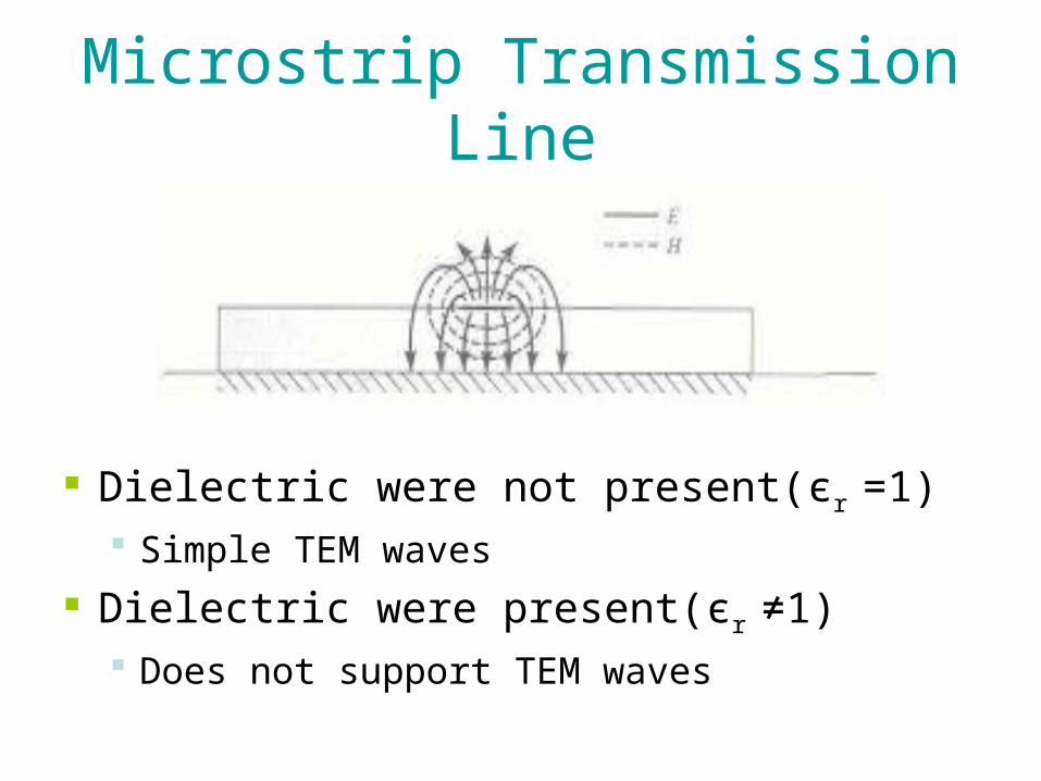
Microstrip Transmission Line
Dielectric were not present(єr =1) Simple TEM waves
Dielectric were present(єr ≠1) Does not support TEM waves

Microstrip Transmission Line
In practical application, h<<λ Fields are quasi-TEM
Єe is the effective dielectric constant
1< єe< єr
p
e
cv
0 ek

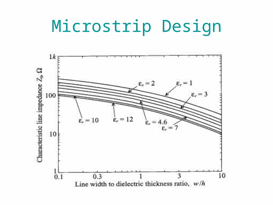
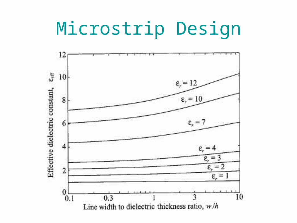
Microstrip Design
Step-1: find W/h ratio
єr and Z0 = known Step-2: For W/h ≤ 2

Microstrip Design
For W/h ≥ 2
Step-3: Effective dielectric constant
Microstrip Design
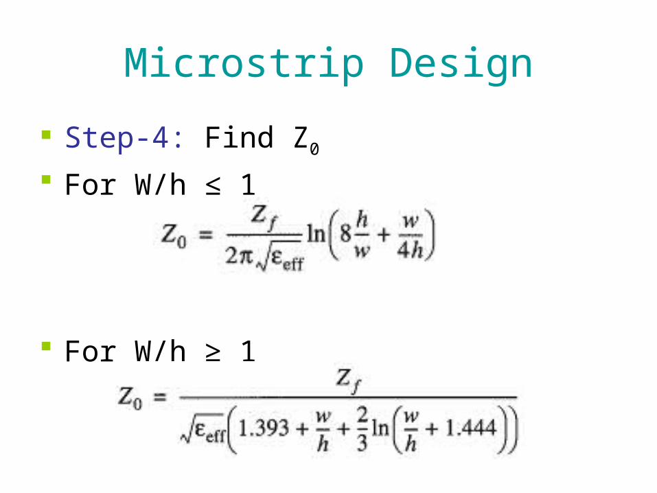
Step-4: Find Z0
For W/h ≤ 1
For W/h ≥ 1

Microstrip Design
Step-5: (1) Attenuation due to dielectric loss
Where tanδ is the loss tangent of the dielectric
0 1 tan/
2 1r e
d
e r
Np m

Microstrip Design
Attenuation due to conductor loss
Rs is the surface resistivity of the conductor
0
0
/
2
sc
s
RNp m
Z W
R
Microstrip Design
Microstrip Design

Design Problems
Problem-1: calculate the width and the length of a microstrip line for a 50Ω characteristic impedance and a 900 phase shift at 2.5 GHz. The substrate thickness is h = 0.127cm, with єr = 2.20
Problem-2: Design a microstrip transmission line for a 100Ω characteristic impedance. The substrate thickness is 0.158cm, with єr = 2.20. What is the guide wavelength on this transmission line if the frequency is 4.0 GHz.
Assignment
Problem: A 100Ω microstrip line is printed on a substrate of thickness 0.0762 cm, with a dielectric constant of 2.2. Ignoring losses and fringing fields, find the shortest length of this line that appears at its input as a capacitor of 2.5 pF at 2.5 GHz. Repeat for an inductance of 5 nH.

Stripline
Most popular type of planer transmission line
Geometry of microstrip line
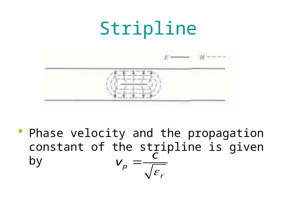
Stripline
Phase velocity and the propagation constant of the stripline is given by
p
r
cv

Stripline
0 rk
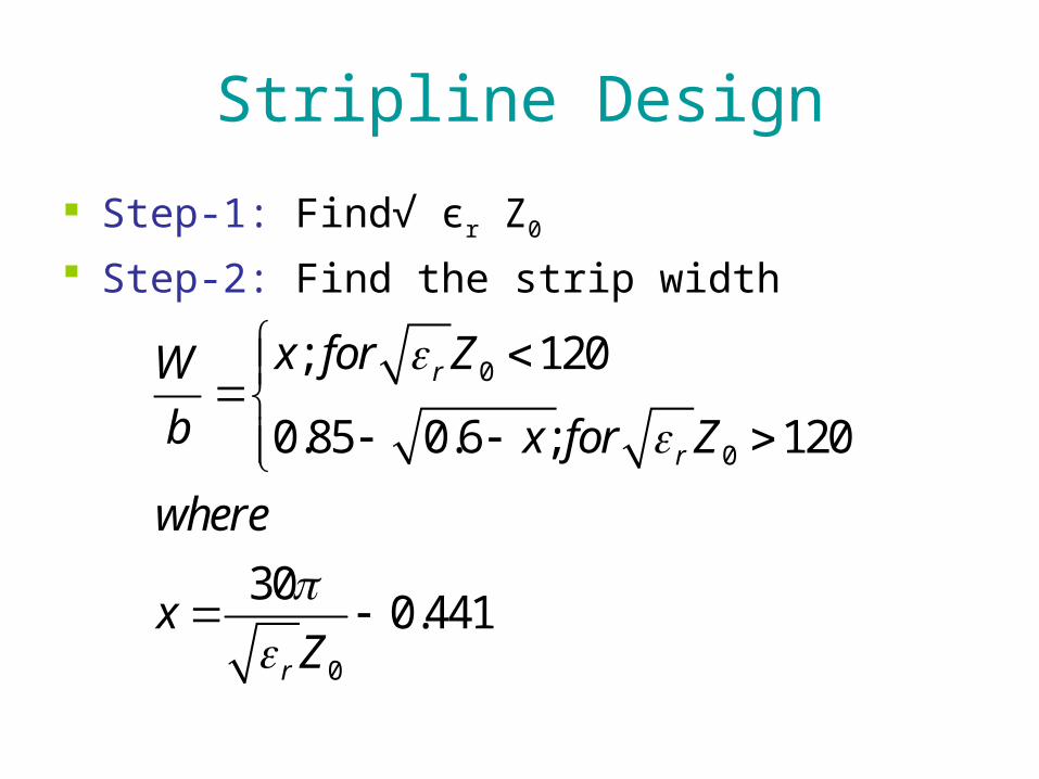
Stripline Design
Step-1: Find√ єr Z0
Step-2: Find the strip width
0
0
0
; 120
0.85 0.6 ; 120
300.441
r
r
r
x for ZW
b x for Z
where
xZ

Stripline Design
• Step-3: Dielectric attenuation
tan
2
2
d
r
k
where
fk
c

Stripline Design
Attenuation due to conductor loss3
00
00
2.7 10120
30 ( )/
0.16120
2 1 21 ln( )
0.414 1 41 (0.5 ln(0.5 0.7 ) 2
s rr
c
sr
R Zfor Z
b tNp m
RBfor Z
Z b
with
W b t b tA
b t b t t
b t WB
W t W t
Stripline Design
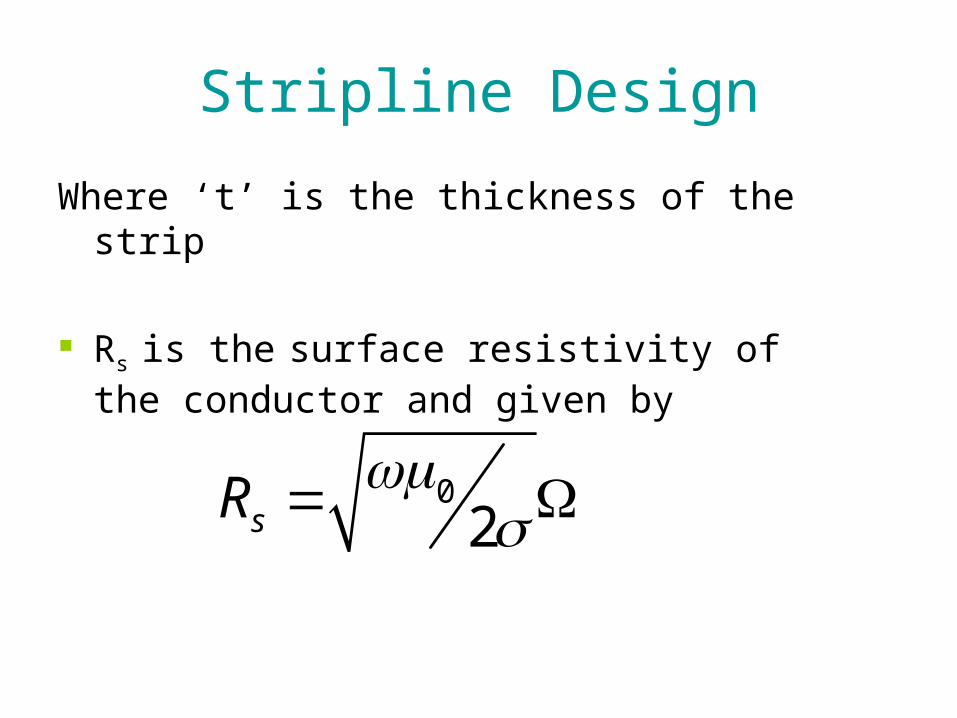
Where ‘t’ is the thickness of the strip
Rs is the surface resistivity of the conductor and given by
02sR
Stripline Design
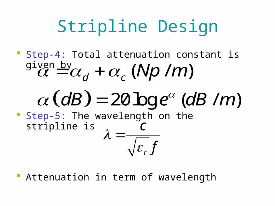
Step-4: Total attenuation constant is given by
Step-5: The wavelength on the stripline is
Attenuation in term of wavelength
( / )
20log ( / )
d c Np m
dB e dB m
r
c
f
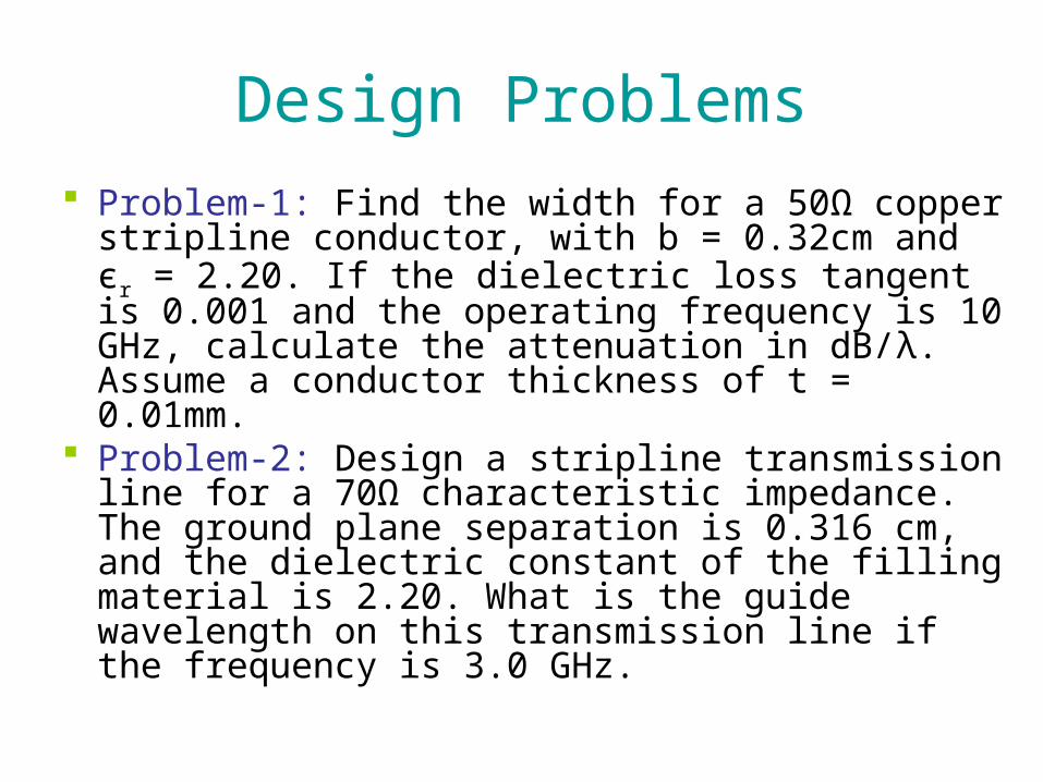
Design Problems
Problem-1: Find the width for a 50Ω copper stripline conductor, with b = 0.32cm and єr = 2.20. If the dielectric loss tangent is 0.001 and the operating frequency is 10 GHz, calculate the attenuation in dB/λ. Assume a conductor thickness of t = 0.01mm.
Problem-2: Design a stripline transmission line for a 70Ω characteristic impedance. The ground plane separation is 0.316 cm, and the dielectric constant of the filling material is 2.20. What is the guide wavelength on this transmission line if the frequency is 3.0 GHz.
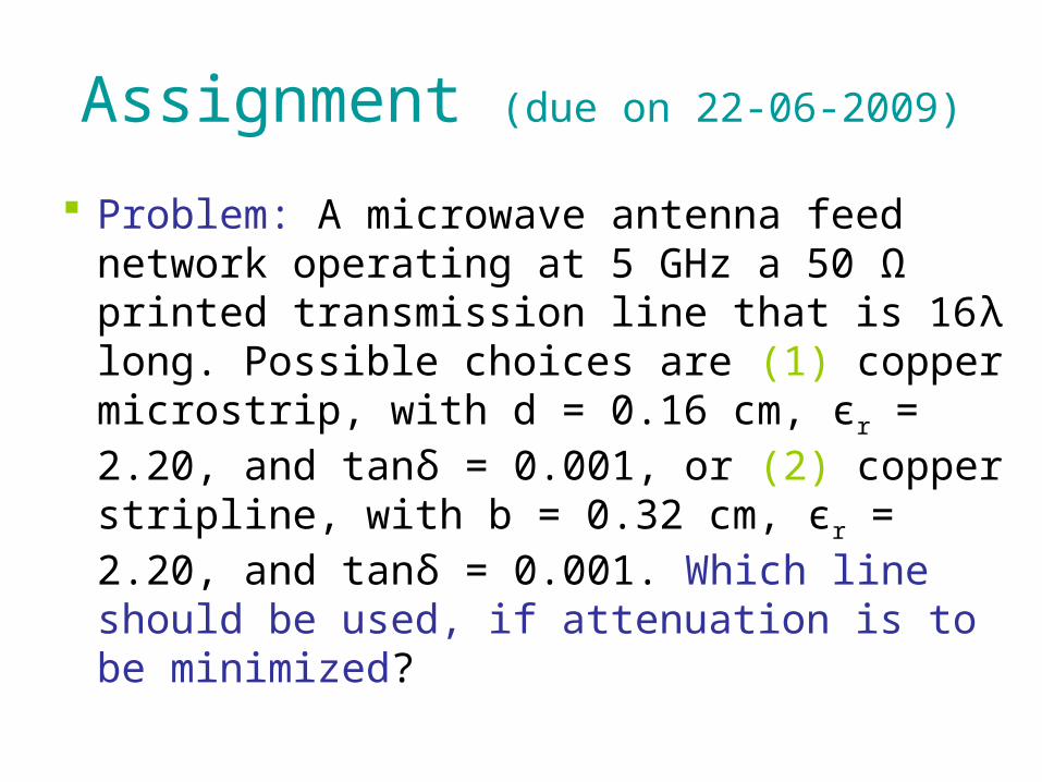
Assignment (due on 22-06-2009)
Problem: A microwave antenna feed network operating at 5 GHz a 50 Ω printed transmission line that is 16λ long. Possible choices are (1) copper microstrip, with d = 0.16 cm, єr = 2.20, and tanδ = 0.001, or (2) copper stripline, with b = 0.32 cm, єr = 2.20, and tanδ = 0.001. Which line should be used, if attenuation is to be minimized?
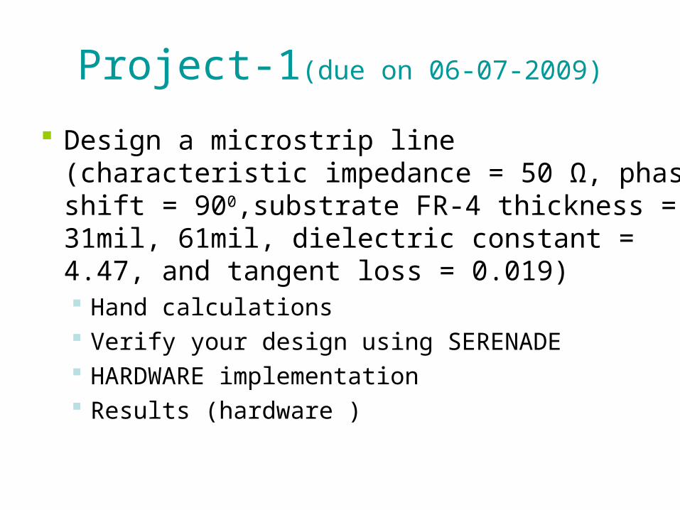
Project-1(due on 06-07-2009)
Design a microstrip line (characteristic impedance = 50 Ω, phase shift = 900,substrate FR-4 thickness = 31mil, 61mil, dielectric constant = 4.47, and tangent loss = 0.019) Hand calculations Verify your design using SERENADE HARDWARE implementation Results (hardware )

Instructions
Each group has two students. Do your own work. Write project report. No late submission.

Instructions
The format for design report should be as follows 1. Title page (including your name, the course number
and the date) Your signature after the statement I certify that this design is the result of my own efforts. (Signature) Date: 2. Design objectives and specifications 3. Design steps (including all, mentioned in problem
statement) 4. Design modifications, if any 5. Computer design verifications 6. Results (hardware) 7. Conclusions