Introduction to VLSI Circuits and Systems, NCUT 2007 Chapter 12 Arithmetic Circuits in CMOS VLSI...
25
Introduction to VLSI Circuits and Systems, NCUT 2007 Chapter 12 Arithmetic Circuits in CMOS VLSI Introduction to VLSI Circuits and Systems 積 積積積積 體 積積積 Dept. of Electronic Engineering National Chin-Yi University of Technology Fall 2007
-
date post
21-Dec-2015 -
Category
Documents
-
view
273 -
download
4
Transcript of Introduction to VLSI Circuits and Systems, NCUT 2007 Chapter 12 Arithmetic Circuits in CMOS VLSI...
Introduction to VLSI Circuits and Systems, NCUT 2007
Chapter 12Arithmetic Circuits in CMOS VLSI
Introduction to VLSI Circuits and Systems積體電路概論
賴秉樑Dept. of Electronic Engineering
National Chin-Yi University of Technology
Fall 2007
Introduction to VLSI Circuits and Systems, NCUT 2007
Outline
Bit Adder Circuits Ripple-Carry Adders Carry Look-Ahead Adders Other High-Speed Adders Multipliers

Introduction to VLSI Circuits and Systems, NCUT 2007
Half-Adder Circuits
Consider two binary digit x and y, and the binary sum is denoted by x + y such that
A half-adder has 2 inputs (x and y) and 2 outputs (the sum s and the carry-out c)
1011
101
110
000
yxs
yxc
Figure 12.1 Half-adder symbol and operation
Figure 12.2 Half-adder logic diagram
(12.1)
(12.2)
Introduction to VLSI Circuits and Systems, NCUT 2007
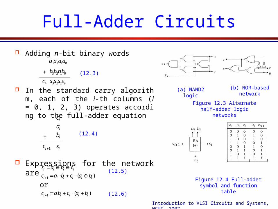
Full-Adder Circuits
Adding n-bit binary words
In the standard carry algorithm, each of the i-th columns (i = 0, 1, 2, 3) operates according to the full-adder equation
Expressions for the network are
0123 aaaa
0123 bbbb
0123 ssss4c
+ (12.3)
ic
ia
ib
is1ic
+ (12.4)
Figure 12.4 Full-adder symbol and function table
)(1 iiiiii
iiii
bacbac
cbas
)(1 iiiiii bacbac
or
Figure 12.3 Alternate half-adder logic networks
(a) NAND2 logic (b) NOR-based network
(12.5)
(12.6)

Introduction to VLSI Circuits and Systems, NCUT 2007
Complementary Pass-transistor Logic
Dual-rail complementary pass-transistor logic (CPL)
iiii baandba
iiiiiin cbacbas )()(
iiii cbba
iiii bacb
iiii cbba
iiii bacb
(12.7)
(12.8)
(12.9)
(12.10)
(12.11)
(12.12)
Figure 12.5 CPL full-adder design
(a) 2-input array (b) Sum circuit
(c) Carry circuit

Introduction to VLSI Circuits and Systems, NCUT 2007
Full-Adder Circuits (1/2)
Figure 12.6 Full-adder logic networks
(a) Gate-level logic
(b) HA-based design
Figure 12.7 AOI full-adder logicFigure 12.8 Evolution of carry-out
circuit
(a) Standard nFET logic
(b) Mirror circuit

Introduction to VLSI Circuits and Systems, NCUT 2007
Full-Adder Circuits (2/2)
Figure 12.9 Mirror AOI CMOS full-adder Figure 12.10 Transmission-gate full-adder circuit
Introduction to VLSI Circuits and Systems, NCUT 2007
Outline
Bit Adder Circuits Ripple-Carry Adders Carry Look-Ahead Adders Other High-Speed Adders Multipliers
Introduction to VLSI Circuits and Systems, NCUT 2007
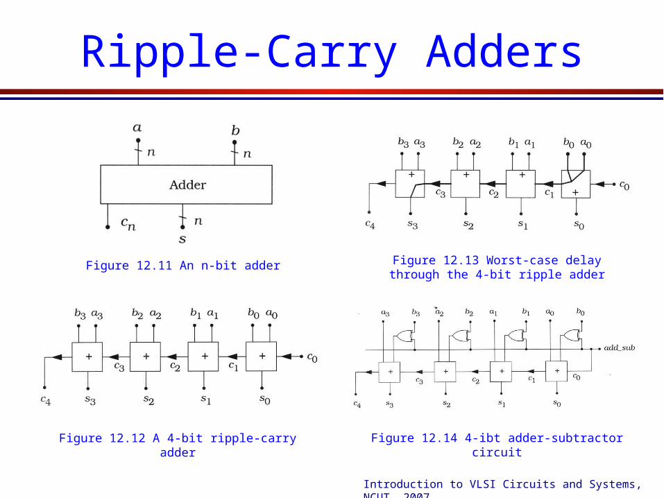
Ripple-Carry Adders
Figure 12.11 An n-bit adder
Figure 12.12 A 4-bit ripple-carry adder
Figure 12.13 Worst-case delay through the 4-bit ripple adder
Figure 12.14 4-ibt adder-subtractor circuit
Introduction to VLSI Circuits and Systems, NCUT 2007
Outline
Bit Adder Circuits Ripple-Carry Adders Carry Look-Ahead Adders Other High-Speed Adders Multipliers
Introduction to VLSI Circuits and Systems, NCUT 2007
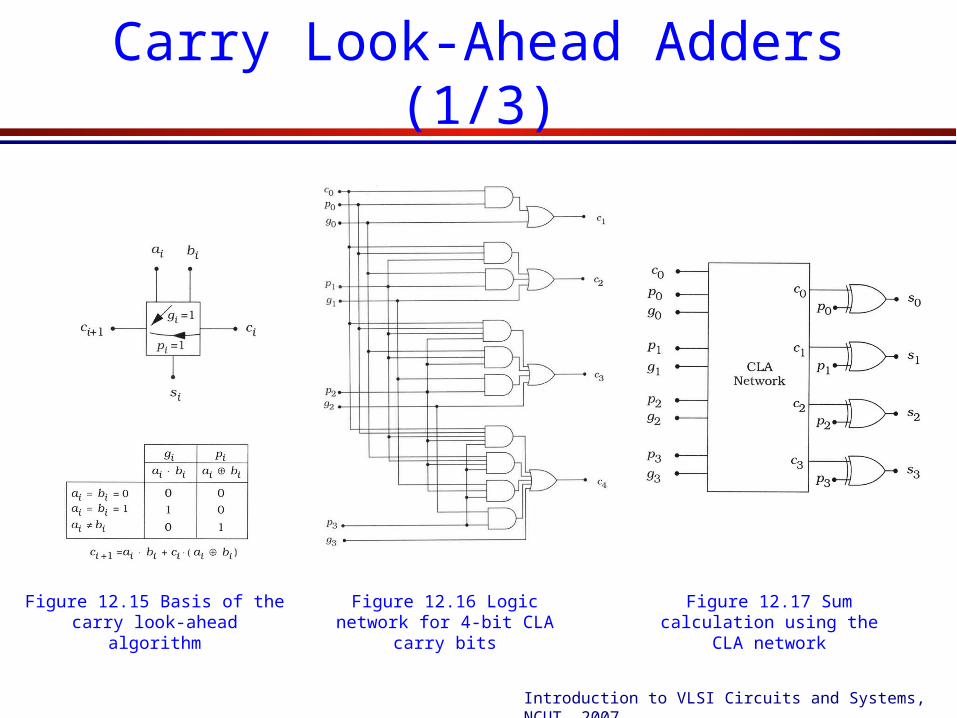
Carry Look-Ahead Adders (1/3)
Figure 12.15 Basis of the carry look-ahead algorithm
Figure 12.16 Logic network for 4-bit CLA carry bits
Figure 12.17 Sum calculation using the CLA
network

Introduction to VLSI Circuits and Systems, NCUT 2007
Carry Look-Ahead Adders (2/3)
Figure 12.18 nFET logic arrays for the CLA terms
(a) C1 logic (b) C2 logic
(c) C3 logic (d) C4 logic
Figure 12.19 Possible uses of the nFET logic arrays in Figure 12.18
(a) Complementary
(b) Pseudo nMOS
(c) Dynamic
Introduction to VLSI Circuits and Systems, NCUT 2007
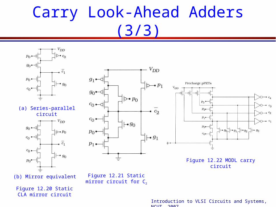
Carry Look-Ahead Adders (3/3)
Figure 12.20 Static CLA mirror circuit
(a) Series-parallel circuit
(b) Mirror equivalent Figure 12.21 Static mirror circuit for C2
Figure 12.22 MODL carry circuit
Introduction to VLSI Circuits and Systems, NCUT 2007
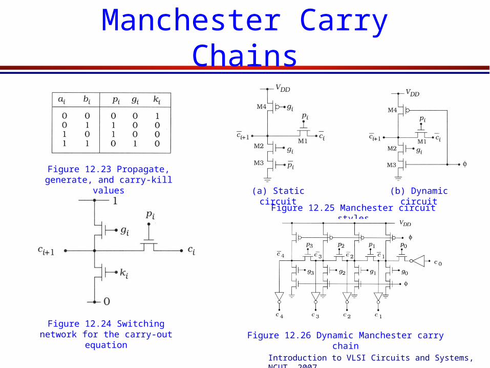
Manchester Carry Chains
Figure 12.23 Propagate, generate, and carry-kill values
Figure 12.24 Switching network for the carry-out
equation
Figure 12.25 Manchester circuit styles
(a) Static circuit (b) Dynamic circuit
Figure 12.26 Dynamic Manchester carry chain
Introduction to VLSI Circuits and Systems, NCUT 2007
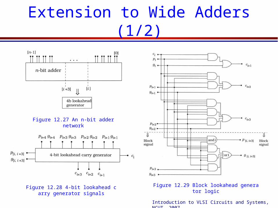
Extension to Wide Adders (1/2)
Figure 12.27 An n-bit adder network
Figure 12.28 4-bit lookahead carry generator signals
Figure 12.29 Block lookahead generator logic

Introduction to VLSI Circuits and Systems, NCUT 2007
Extension to Wide Adders (2/2)
Figure 12.30 Multilevel CLA block scheme for a 16-bit adder
Figure 12.31 64-bit CLA architecture
Introduction to VLSI Circuits and Systems, NCUT 2007
Outline
Bit Adder Circuits Ripple-Carry Adders Carry Look-Ahead Adders Other High-Speed Adders Multipliers
Introduction to VLSI Circuits and Systems, NCUT 2007
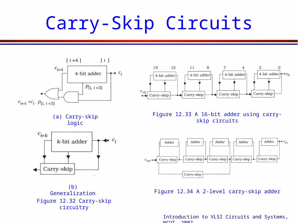
Carry-Skip Circuits
Figure 12.32 Carry-skip circuitry
(a) Carry-skip logic
(b) Generalization
Figure 12.33 A 16-bit adder using carry-skip circuits
Figure 12.34 A 2-level carry-skip adder
Introduction to VLSI Circuits and Systems, NCUT 2007
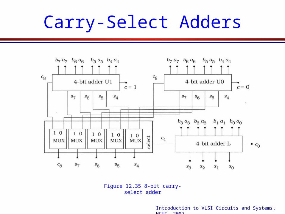
Carry-Select Adders
Figure 12.35 8-bit carry-select adder

Introduction to VLSI Circuits and Systems, NCUT 2007
Carry-Save Adders
Figure 12.36 Basic of a carry-save adder
(a) Symbol
(b) 3-to-2 reduction
Figure 12.37 Creation of an n-bit carry-save adder
Introduction to VLSI Circuits and Systems, NCUT 2007
Outline
Bit Adder Circuits Ripple-Carry Adders Carry Look-Ahead Adders Other High-Speed Adders Multipliers
Introduction to VLSI Circuits and Systems, NCUT 2007
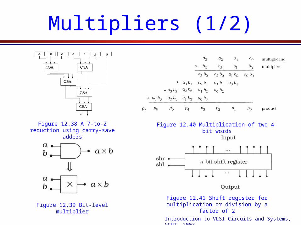
Multipliers (1/2)
Figure 12.38 A 7-to-2 reduction using carry-save adders
Figure 12.39 Bit-level multiplier
Figure 12.40 Multiplication of two 4-bit words
Figure 12.41 Shift register for multiplication or division by a factor of 2
Introduction to VLSI Circuits and Systems, NCUT 2007
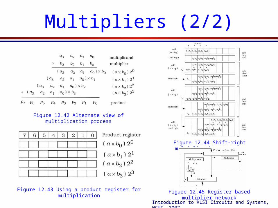
Multipliers (2/2)
Figure 12.42 Alternate view of multiplication process
Figure 12.43 Using a product register for multiplication
Figure 12.44 Shift-right multiplication sequence
Figure 12.45 Register-based multiplier network
Introduction to VLSI Circuits and Systems, NCUT 2007
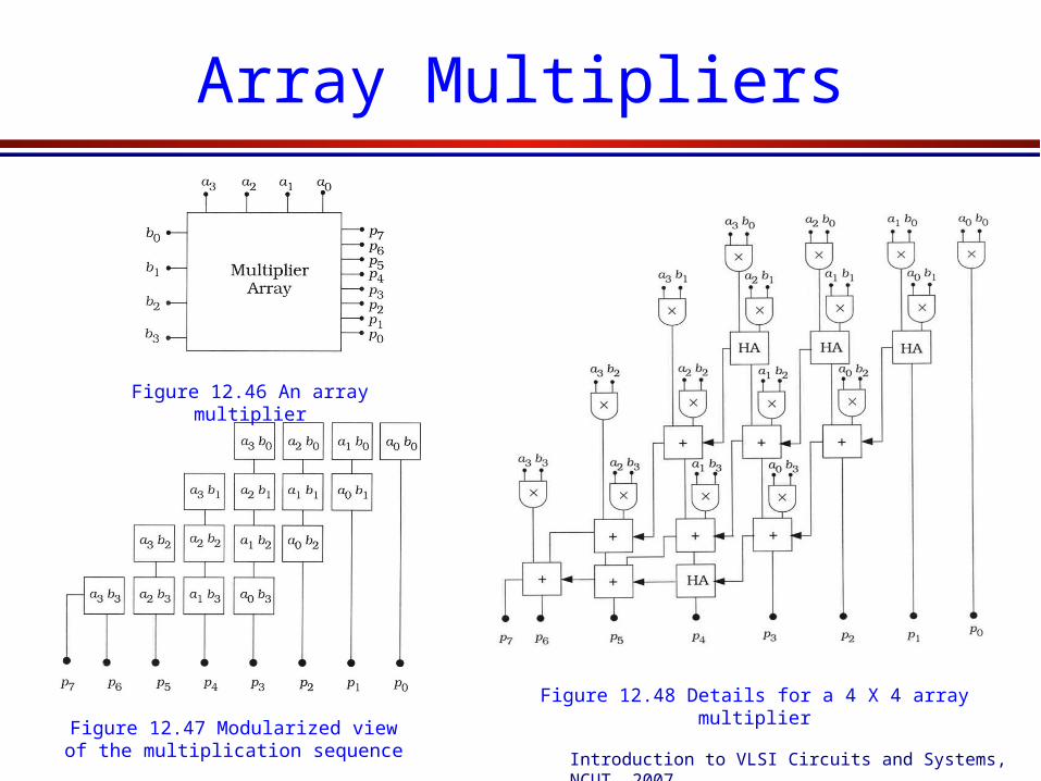
Array Multipliers
Figure 12.46 An array multiplier
Figure 12.47 Modularized view of the multiplication sequence
Figure 12.48 Details for a 4 X 4 array multiplier
Introduction to VLSI Circuits and Systems, NCUT 2007
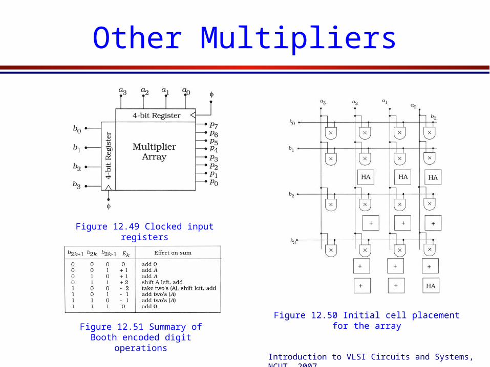
Other Multipliers
Figure 12.49 Clocked input registers
Figure 12.50 Initial cell placement for the arrayFigure 12.51 Summary of Booth
encoded digit operations