
Introduction to Logic Analysis - · PDF fileiv Introduction to Logic Analysis: A Hardware...
56
L o g i c A n a l y z e r s Introduction to Logic Analysis A Hardware Debug Tutorial
-
Upload
phungkhuong -
Category
Documents
-
view
230 -
download
1
Transcript of Introduction to Logic Analysis - · PDF fileiv Introduction to Logic Analysis: A Hardware...

Lo
gi
c
An
al
yz
er
s
Introduction to Logic AnalysisA Hardware Debug Tutorial


www.tektronix.com/LA i
Introduction to Logic AnalysisA Hardware Debug Tutorial

ii
Introduction to Logic Analysis: A Hardware Debug TutorialTutorial
www.tektronix.com/LA

Introduction to Logic Analysis: A Hardware Debug TutorialTutorial
www.tektronix.com/LA iii
Contents
Introduction· · · · · · · · · · · · · · · · · · · · · · · · · · · · · · · · · · · · · · · · · · · · · · · · · · · vi
Getting Started· · · · · · · · · · · · · · · · · · · · · · · · · · · · · · · · · · · · · · · · · · · · · · · · · 1Requirements · · · · · · · · · · · · · · · · · · · · · · · · · · · · · · · · · · · · · · · · · · · · · · · · · · · · · · · · · · · · · · · · 1
Setting up the Logic Analyzer · · · · · · · · · · · · · · · · · · · · · · · · · · · · · · · · · · · · · · · · · · · · · · · · · · · · 2
Connecting to the Training Board · · · · · · · · · · · · · · · · · · · · · · · · · · · · · · · · · · · · · · · · · · · · · · · · · 3
TLA7QS QuickStart Training Board Power Connections · · · · · · · · · · · · · · · · · · · · · · · · · · · · · · · · · 4
Installing the Tutorial Setup Files · · · · · · · · · · · · · · · · · · · · · · · · · · · · · · · · · · · · · · · · · · · · · · · · · · 5Copy Tutorial Files to Logic Analyzer · · · · · · · · · · · · · · · · · · · · · · · · · · · · · · · · · · · · · · · · · · · · · · · · · · · · · · 5
D-Type Flip-Flop · · · · · · · · · · · · · · · · · · · · · · · · · · · · · · · · · · · · · · · · · · · · · · · · · · · · · · · · · · · · · · 5
Getting Familiar with TLA Basics · · · · · · · · · · · · · · · · · · · · · · · · · · · · · · · · · · · 7TLA User Interface Overview · · · · · · · · · · · · · · · · · · · · · · · · · · · · · · · · · · · · · · · · · · · · · · · · · · · · 8
Power Up the TLA · · · · · · · · · · · · · · · · · · · · · · · · · · · · · · · · · · · · · · · · · · · · · · · · · · · · · · · · · · · · 8
Load Default System and View TLA Windows · · · · · · · · · · · · · · · · · · · · · · · · · · · · · · · · · · · · · · · · 8
System Window · · · · · · · · · · · · · · · · · · · · · · · · · · · · · · · · · · · · · · · · · · · · · · · · · · · · · · · · · · · · · · 8
Run · · · · · · · · · · · · · · · · · · · · · · · · · · · · · · · · · · · · · · · · · · · · · · · · · · · · · · · · · · · · · · · · · · · · · · · 10
Alternative Method of Navigating the TLA Application Windows · · · · · · · · · · · · · · · · · · · · · · · · · · 11
What You Learned · · · · · · · · · · · · · · · · · · · · · · · · · · · · · · · · · · · · · · · · · · · · · · · · · · · · · · · · · · · · 12
Tutorial 1 – General Purpose Timing· · · · · · · · · · · · · · · · · · · · · · · · · · · · · · · · · 13Load the Setup and Run · · · · · · · · · · · · · · · · · · · · · · · · · · · · · · · · · · · · · · · · · · · · · · · · · · · · · · · 13
View the Data and Make a Timing Measurement · · · · · · · · · · · · · · · · · · · · · · · · · · · · · · · · · · · · · 15
View the Trigger Setup · · · · · · · · · · · · · · · · · · · · · · · · · · · · · · · · · · · · · · · · · · · · · · · · · · · · · · · · 16
View the Channel Setups · · · · · · · · · · · · · · · · · · · · · · · · · · · · · · · · · · · · · · · · · · · · · · · · · · · · · · · 16
What You Learned · · · · · · · · · · · · · · · · · · · · · · · · · · · · · · · · · · · · · · · · · · · · · · · · · · · · · · · · · · · · 17
Tutorial 2 – Glitch Detection and Display · · · · · · · · · · · · · · · · · · · · · · · · · · · · · 19Load the Setup from Tutorial 1 · · · · · · · · · · · · · · · · · · · · · · · · · · · · · · · · · · · · · · · · · · · · · · · · · · · 19
Introduction to Logic Analysis: A Hardware Debug Tutorial

iv
Introduction to Logic Analysis: A Hardware Debug TutorialTutorial
www.tektronix.com/LA
Modify an Existing Trigger Setup · · · · · · · · · · · · · · · · · · · · · · · · · · · · · · · · · · · · · · · · · · · · · · · · · 19
Run · · · · · · · · · · · · · · · · · · · · · · · · · · · · · · · · · · · · · · · · · · · · · · · · · · · · · · · · · · · · · · · · · · · · · · 20
View the Data · · · · · · · · · · · · · · · · · · · · · · · · · · · · · · · · · · · · · · · · · · · · · · · · · · · · · · · · · · · · · · · 20
Change the Acquisition Mode to Glitches · · · · · · · · · · · · · · · · · · · · · · · · · · · · · · · · · · · · · · · · · · · 21
Run · · · · · · · · · · · · · · · · · · · · · · · · · · · · · · · · · · · · · · · · · · · · · · · · · · · · · · · · · · · · · · · · · · · · · · · 21
View the Data · · · · · · · · · · · · · · · · · · · · · · · · · · · · · · · · · · · · · · · · · · · · · · · · · · · · · · · · · · · · · · · 21
Adding High Speed Timing (MagniVu™) to the Display · · · · · · · · · · · · · · · · · · · · · · · · · · · · · · · · · 22
Changing the Height of the Displayed Channels · · · · · · · · · · · · · · · · · · · · · · · · · · · · · · · · · · · · · 23
View the Glitch · · · · · · · · · · · · · · · · · · · · · · · · · · · · · · · · · · · · · · · · · · · · · · · · · · · · · · · · · · · · · · 23
Measure Glitch Pulse Width · · · · · · · · · · · · · · · · · · · · · · · · · · · · · · · · · · · · · · · · · · · · · · · · · · · · 24
Document the Glitch · · · · · · · · · · · · · · · · · · · · · · · · · · · · · · · · · · · · · · · · · · · · · · · · · · · · · · · · · · 25
Copy and Paste Entire Screen · · · · · · · · · · · · · · · · · · · · · · · · · · · · · · · · · · · · · · · · · · · · · · · · · · 25
Save Your Glitch Setup · · · · · · · · · · · · · · · · · · · · · · · · · · · · · · · · · · · · · · · · · · · · · · · · · · · · · · · · 25
What You Learned · · · · · · · · · · · · · · · · · · · · · · · · · · · · · · · · · · · · · · · · · · · · · · · · · · · · · · · · · · · 26
Tutorial 3 – Capture a Setup or Hold Violation · · · · · · · · · · · · · · · · · · · · · · · · · 27Load the Setup and Run · · · · · · · · · · · · · · · · · · · · · · · · · · · · · · · · · · · · · · · · · · · · · · · · · · · · · · · 27
View the Resultant Data · · · · · · · · · · · · · · · · · · · · · · · · · · · · · · · · · · · · · · · · · · · · · · · · · · · · · · · 28
View the Trigger Setup · · · · · · · · · · · · · · · · · · · · · · · · · · · · · · · · · · · · · · · · · · · · · · · · · · · · · · · · 28
What You Learned · · · · · · · · · · · · · · · · · · · · · · · · · · · · · · · · · · · · · · · · · · · · · · · · · · · · · · · · · · · 29
Tutorial 4 – Transitional Storage · · · · · · · · · · · · · · · · · · · · · · · · · · · · · · · · · · · 31Load the Setup for Conventional Timing and Run · · · · · · · · · · · · · · · · · · · · · · · · · · · · · · · · · · · · · 31
View the Resultant Data · · · · · · · · · · · · · · · · · · · · · · · · · · · · · · · · · · · · · · · · · · · · · · · · · · · · · · · 31
Modify the Trigger for Transitional Timing · · · · · · · · · · · · · · · · · · · · · · · · · · · · · · · · · · · · · · · · · · 32
Run and View the Acquired Data Using Transitional Storage · · · · · · · · · · · · · · · · · · · · · · · · · · · · 32
Save Your Transitional Timing Setup · · · · · · · · · · · · · · · · · · · · · · · · · · · · · · · · · · · · · · · · · · · · · · 33
Pre-configured Transitional Timing Setup · · · · · · · · · · · · · · · · · · · · · · · · · · · · · · · · · · · · · · · · · · · 33
What You Learned · · · · · · · · · · · · · · · · · · · · · · · · · · · · · · · · · · · · · · · · · · · · · · · · · · · · · · · · · · · 33
Tutorial 5 – How to Create Setups · · · · · · · · · · · · · · · · · · · · · · · · · · · · · · · · · 35Load the Default Setup · · · · · · · · · · · · · · · · · · · · · · · · · · · · · · · · · · · · · · · · · · · · · · · · · · · · · · · · 35
Delete Default Data Windows · · · · · · · · · · · · · · · · · · · · · · · · · · · · · · · · · · · · · · · · · · · · · · · · · · · 35
www.tektronix.com/LA v
Define the Setup Window · · · · · · · · · · · · · · · · · · · · · · · · · · · · · · · · · · · · · · · · · · · · · · · · · · · · · · 35
Define New Channels and Groups · · · · · · · · · · · · · · · · · · · · · · · · · · · · · · · · · · · · · · · · · · · · · · · · 35
Assign Channels to Groups · · · · · · · · · · · · · · · · · · · · · · · · · · · · · · · · · · · · · · · · · · · · · · · · · · · · · 37
Complete the Setup Window · · · · · · · · · · · · · · · · · · · · · · · · · · · · · · · · · · · · · · · · · · · · · · · · · · · · 37
Define the Trigger Window · · · · · · · · · · · · · · · · · · · · · · · · · · · · · · · · · · · · · · · · · · · · · · · · · · · · · 37
Define the Waveform Window · · · · · · · · · · · · · · · · · · · · · · · · · · · · · · · · · · · · · · · · · · · · · · · · · · · 38Create a New Waveform Window · · · · · · · · · · · · · · · · · · · · · · · · · · · · · · · · · · · · · · · · · · · · · · · · · · · · · · · 38
Run · · · · · · · · · · · · · · · · · · · · · · · · · · · · · · · · · · · · · · · · · · · · · · · · · · · · · · · · · · · · · · · · · · · · · · · · · · · · · · 38
Create a MagniVu™ Waveform Window (Optional) · · · · · · · · · · · · · · · · · · · · · · · · · · · · · · · · · · · 38
Save Your Setup · · · · · · · · · · · · · · · · · · · · · · · · · · · · · · · · · · · · · · · · · · · · · · · · · · · · · · · · · · · · · 39
What You Learned · · · · · · · · · · · · · · · · · · · · · · · · · · · · · · · · · · · · · · · · · · · · · · · · · · · · · · · · · · · 40
Resources for You · · · · · · · · · · · · · · · · · · · · · · · · · · · · · · · · · · · · · · · · · · · · · 41Tektronix Logic Analyzers on the Web · · · · · · · · · · · · · · · · · · · · · · · · · · · · · · · · · · · · · · · · · · · · · 41
Technical Support · · · · · · · · · · · · · · · · · · · · · · · · · · · · · · · · · · · · · · · · · · · · · · · · · · · · · · · · · · · · 41
XYZs of Logic Analyzers · · · · · · · · · · · · · · · · · · · · · · · · · · · · · · · · · · · · · · · · · · · · · · · · · · · · · · · 41
QuickStart Training Manual · · · · · · · · · · · · · · · · · · · · · · · · · · · · · · · · · · · · · · · · · · · · · · · · · · · · · 42
Tutorial CD-ROM · · · · · · · · · · · · · · · · · · · · · · · · · · · · · · · · · · · · · · · · · · · · · · · · · · · · · · · · · · · · · 42
TLAVu · · · · · · · · · · · · · · · · · · · · · · · · · · · · · · · · · · · · · · · · · · · · · · · · · · · · · · · · · · · · · · · · · · · · · 42
Appendix · · · · · · · · · · · · · · · · · · · · · · · · · · · · · · · · · · · · · · · · · · · · · · · · · · · · 43Installation of TLAVu on a PC · · · · · · · · · · · · · · · · · · · · · · · · · · · · · · · · · · · · · · · · · · · · · · · · · · · 43
Viewing Data · · · · · · · · · · · · · · · · · · · · · · · · · · · · · · · · · · · · · · · · · · · · · · · · · · · · · · · · · · · · · · · 43
Load System · · · · · · · · · · · · · · · · · · · · · · · · · · · · · · · · · · · · · · · · · · · · · · · · · · · · · · · · · · · · · · · 43
New Data Window · · · · · · · · · · · · · · · · · · · · · · · · · · · · · · · · · · · · · · · · · · · · · · · · · · · · · · · · · · · 44
Load Data Window · · · · · · · · · · · · · · · · · · · · · · · · · · · · · · · · · · · · · · · · · · · · · · · · · · · · · · · · · · · 44
Technical Support · · · · · · · · · · · · · · · · · · · · · · · · · · · · · · · · · · · · · · · · · · · · · · · · · · · · · · · · · · · 44
Introduction to Logic Analysis: A Hardware Debug TutorialTutorial

vi
Introduction to Logic Analysis: A Hardware Debug TutorialTutorial
www.tektronix.com/LAvi
This Tutorial booklet contains selected exercises designed to quickly familiarize
you with using the TLA logic analyzer and to make typical timing measurements
useful in hardware debug of digital circuits. In addition, you will be introduced
to the basic operation of the TLA as well as key features that can enable you to
debug your digital designs quicker and more efficiently. The TLA600 and
TLA700 Series logic analyzers use the same powerful, yet intuitive, Windows
interface and application software. This allows users to learn on one logic ana-
lyzer and easily use any other member of the TLA family.
After using this booklet, you can easily begin making most standard timing
measurements required to debug your own applications. For those users who
would like to fully explore the powerful TLA platform, the TLA7QS Training
Manual is a rich collection of exercises based on the target board used in this
tutorial. This is available through the Tektronix sales office nearest you or can
be downloaded on the web (see information in Resources for You at the end of
this booklet). You can also explore the TLA user interface without a logic ana-
lyzer by using TLAVu, an offline version of the TLA application software
included on the Tutorial CD-ROM, that you can load on your PC. TLAVu comes
with both hardware and software debug examples.
The focus of this tutorial is on "hardware debug" which fundamentally is about
making critical digital timing measurements and the detection of elusive prob-
lems such as glitches and setup/hold violations. We will also introduce you to
the powerful TLA user interface and its philosophy of operation.
This Tutorial assumes that you:
are familiar with Microsoft Windows
have a basic understanding of digital electronics
are looking for faster digital debug solutions
If you are unfamiliar with logic analyzer concepts, it is suggested that you read
the XYZs of Logic Analyzers. You can also get a printed version of the XYZs by
going online at
www.Tektronix.com/TLA
Introduction

Requirements
Any TLA600 Series logic analyzer
Version 3.2 or greater software installed on logic
analyzer
Keyboard and mouse
P6418 probe
Tutorial booklet
Tutorial CD-ROM
TLA7QS QuickStart training board with power
adapter
Note: If you are using a TLA60x series or a
72x series logic analyzer, be aware that the
front-panel adjustments referred to in this
tutorial will be unavailable to you. However,
they are available under mouse control.
Introduction to Logic Analysis: A Hardware Debug TutorialTutorial
www.tektronix.com/LA 1
Figure 1-1: TLA61x/62x Tutorial components.
Getting Started

2
Introduction to Logic Analysis: A Hardware Debug TutorialTutorial
www.tektronix.com/LA
Setting up the LogicAnalyzer
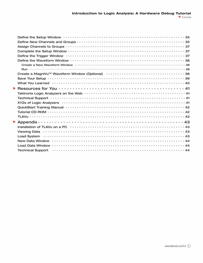
1. For the following steps refer to Figure 1-2.
2. Connect the AC line cord to the logic analyzer AC
line input connector located on the rear panel.
3. Connect the mouse and the keyboard to the rear
panel.
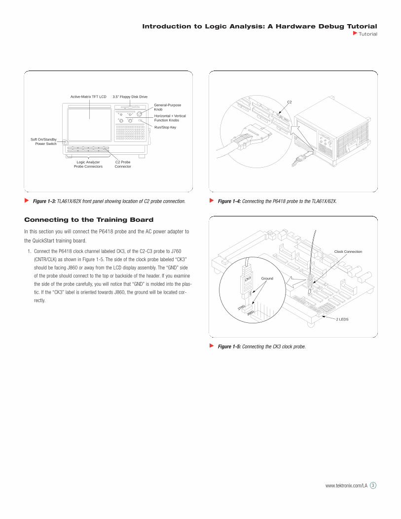
4. Connect the P6418 probe to the C2/C3 connector,
which is located on the lower front panel of the
TLA600 logic analyzer as shown in Figure 1-3 and
Figure 1-4. (This will be located on the right hand
side of the analyzer if you are using a TLA714).
The probe should be oriented with the slotted key
facing upwards. Press the probe into the logic ana-
lyzer connector firmly.
Figure 1-2: TLA600 rear-panel connections.
AC PowerFusesPrimary ON/OFFPower Switch
CD-ROMKeyboardPS2 Port
MousePS2 Port
Connecting to the Training Board
In this section you will connect the P6418 probe and the AC power adapter to
the QuickStart training board.
1. Connect the P6418 clock channel labeled CK3, of the C2-C3 probe to J760
(CNTR/CLK) as shown in Figure 1-5. The side of the clock probe labeled “CK3”
should be facing J860 or away from the LCD display assembly. The “GND” side
of the probe should connect to the top or backside of the header. If you examine
the side of the probe carefully, you will notice that “GND” is molded into the plas-
tic. If the “CK3” label is oriented towards J860, the ground will be located cor-
rectly.
Introduction to Logic Analysis: A Hardware Debug TutorialTutorial
www.tektronix.com/LA 3
Figure 1-3: TLA61X/62X front panel showing location of C2 probe connection.
General-PurposeKnob
Run/Stop Key
Logic AnalyzerProbe Connectors
C2 ProbeConnector
Active-Matrix TFT LCD
Soft On/StandbyPower Switch
Horizontal + VerticalFunction Knobs
3.5" Floppy Disk Drive
Figure 1-4: Connecting the P6418 probe to the TLA61X/62X.
C2
Figure 1-5: Connecting the CK3 clock probe.
Ground
Clock Connection
2 LEDS

4
2. Connect the P6418 C2 probe directly over the entire header J860 as shown in
Figure 1-6. Make sure that the side of the probe labeled C2 7------0 is
facing towards the front of the training board (towards the LEDs). The rear
pins on the header are all ground pins.
TLA7QS QuickStart Training Board PowerConnections
1. Connect the power adapter to the DC power input jack at the rear left corner of
the training board as shown in Figure 1-6 and plug into an appropriate AC
source.
2. Apply power to the training board by toggling switch S110 to the “On” position
(move switch towards green LED). The adjacent green LED should now be on.
3. The training board will execute the power-on diagnostics. When the power-on
diagnostics are complete, the display should display some menu text and two of
the LEDs should be lit. The training board is now ready.
Introduction to Logic Analysis: A Hardware Debug TutorialTutorial
www.tektronix.com/LA
Figure 1-6: Connecting the P6418 C2 probe to header J860 – label shown fac-ing towards signal side of header J860.
C2 Probe Connector
Clock Connection
2 LEDS
Pull Tab
Power ConnectionS110 Switch
Installing the Tutorial Setup Files
Copy Tutorial Files to Logic Analyzer
1. Open the CD-ROM located on the rear panel of the TLA600 Series logic analyzer
and load the Tutorial CD-ROM.
2. Using Windows Explorer, locate the tutorial setup files on the CD-ROM in the
folder:
D:\Tutorial\Hardware\Setups\*.tla
3. Copy these files to the following location on the logic analyzer’s hard drive:
C:\Program Files\TLA 700\Tutorial\Hardware\
Note: If the folders \Tutorial\Hardware\ are not present on your TLA, cre-
ate these under Program Files/TLA 700.
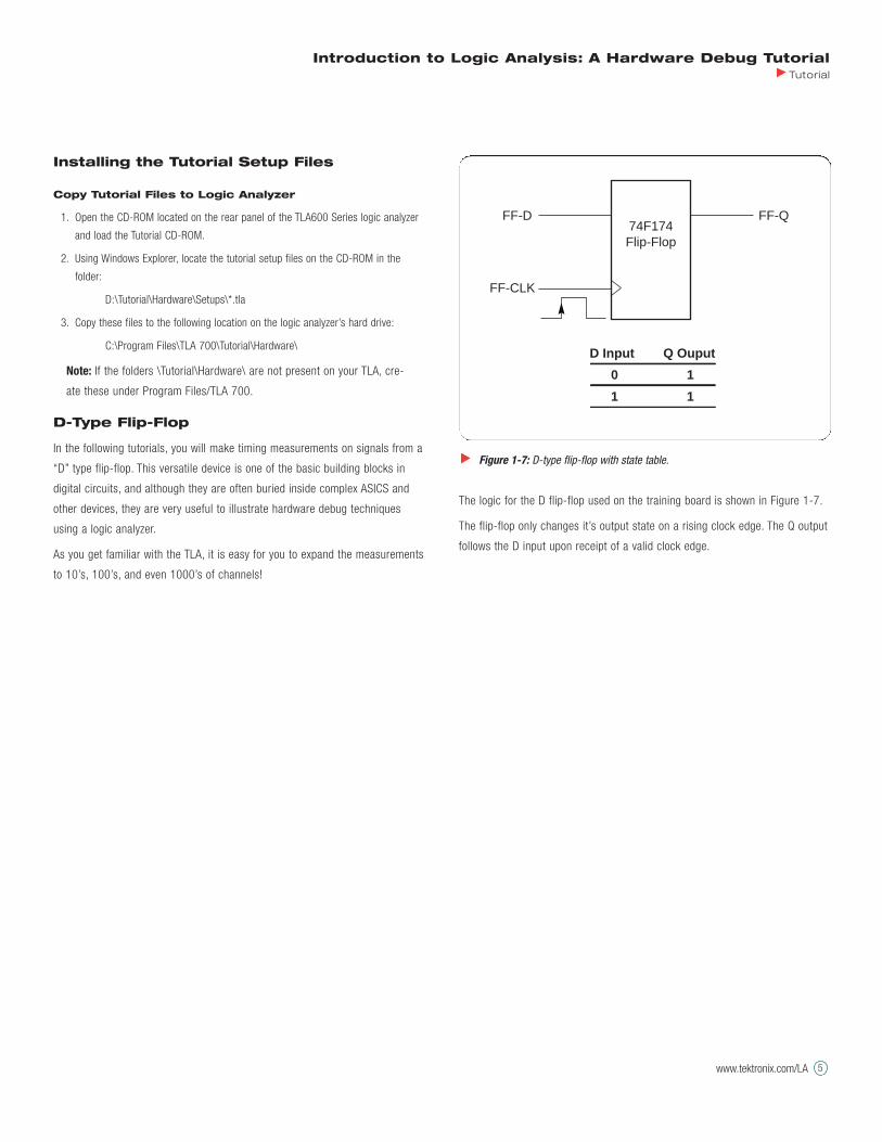
D-Type Flip-Flop
In the following tutorials, you will make timing measurements on signals from a
“D” type flip-flop. This versatile device is one of the basic building blocks in
digital circuits, and although they are often buried inside complex ASICS and
other devices, they are very useful to illustrate hardware debug techniques
using a logic analyzer.
As you get familiar with the TLA, it is easy for you to expand the measurements
to 10’s, 100’s, and even 1000’s of channels!
The logic for the D flip-flop used on the training board is shown in Figure 1-7.
The flip-flop only changes it’s output state on a rising clock edge. The Q output
follows the D input upon receipt of a valid clock edge.
Introduction to Logic Analysis: A Hardware Debug TutorialTutorial
www.tektronix.com/LA 5
Figure 1-7: D-type flip-flop with state table.
FF-CLK
FF-D FF-Q74F174Flip-Flop
D Input Q Ouput
0 1
1 1

6
Introduction to Logic Analysis: A Hardware Debug TutorialTutorial
www.tektronix.com/LA

When using a logic analyzer, it is useful to understand the basic steps in set-
ting up the instrument to take an acquisition. These steps are fundamental to
all logic analyzers regardless of manufacturer. Where differences occur is in
how the user interface is implemented. In this introduction tutorial, we will
explore the main windows that you will be interacting with, and will reinforce
this with practical examples in the subsequent tutorials. You will make use of
saved or modified setups, and the last tutorial will guide you through the
process of creating your own setup so that you can apply what you learned to
your own application.
The fundamental steps and windows involved in setting up the TLA to take an
acquisition are:
1. User loads the default system or loads a saved setup.
2. System Window – this is the starting point for using the other windows.
3. Setup Window – configure the TLA to the physical connections on the target.
4. Trigger Window – set up the trigger conditions.
5. Run – acquire the data.
6. Data Window – set up how and what data will be displayed.
Introduction to Logic Analysis: A Hardware Debug TutorialTutorial
www.tektronix.com/LA 7
Figure 2-1: Basic steps in setting up a TLA to take an acquisition.
2. Go to the System window. This is themain access point to the windows
1. Load (Default System)or (Saved Setup)
Hard DriveFloppy
3. Use the Setup windowsto configure the Logic Analyzer
4. Use the LA Trigger window,to configure the trigger conditions
5. Click the Run tool barbutton to acquire data
Modify Setup/Triggerto acquire new data6. View data in the Listing
and Waveform windows
Getting Familiar with TLA Basics

8
TLA User Interface Overview
The logic analyzer user interface is a Windows-based application. You will use
many familiar controls, such as Cut, Copy, Paste, toolbar buttons, and click-
ing/dragging screen elements. Many powerful features can be invoked using
the right mouse button, such as placement of cursors, zoom in on an area of
interest, etc. In the following tutorials, you will be introduced to many of these
TLA user interface features.
Power Up the TLA
First, ensure that the rear-panel power switch (see Figure 1-2) is in the “On”
position. Then, power up the TLA600 logic analyzer by pressing the power
switch located on the lower left front panel. The TLA will power up with
Windows and one of three possible setups depending on what user option
“Start-Up option” is set:
1. Last System open in previous session
2. Default System Setup
3. Saved System
Load Default System and ViewTLA Windows
In this section, you will place the TLA into its known “Default System Setup”
state. You will then open and examine each of the key windows that we will be
working with in the rest of the tutorials.
1. On the top menu bar, select “File” and “Default System” with your mouse.
2. When the dialog box comes up warning you “This operation will default the cur-
rent system configuration… etc.,” select “OK.”
The TLA will load the default system configuration and present the System
Window, which should look similar to the screen in Figure 2-2 taken from a
TLA624.
System Window
The System Window, shown in Figure 2-2, is the main access point to the other
TLA windows. By clicking on the various buttons, you can go directly to the
Setup, Trigger, and Data (Waveform, Listing) Windows.
Alternately, you can use the “Window” pull-down menu on the main menu bar
or use “Cntrl” + “Tab” to select the same windows. It should be noted that we
will not be using the “Listing 1” Window in these tutorials, since it is used for
state and assembly code listing.
1. Using your mouse, left click on the “Setup” button in the System Window. This
opens the Setup window as shown in Figure 2-3.
Introduction to Logic Analysis: A Hardware Debug TutorialTutorial
www.tektronix.com/LA
Figure 2-2: Default System Window.
Click here to go toSetup Window
Click here to go toTrigger Window
Click here to go toWaveform Window

Setup Window
The Setup Window shown in Figure 2-3, consists of three main sections.
These are (from top to bottom):
a) Acquisition control
This is where clocking is set for internal (asynchronous), or external (synchro-
nous), acquisition mode is set (normal, glitch, block), and sampling speed
selected. In addition, memory depth and logic thresholds are set here. “Show
Activity" provides a function similar to a logic probe so that the user can
check for proper connections.
b) Group section
In this section, the user creates channel groups. A channel group can consist
of one or several channels. All channels must belong to a group even if there
is only one channel in the group. Groups are typically created prior to chan-
nel assignments.
c) Probe/channel assignment section
This is where the user maps the probe physical connections to the logic ana-
lyzer user interface and to a group. All of the probes available will be shown
in the left column labeled “Probe.” Each physical probe has 16 channels and
one clock (CK) or one qualifier (Q). There are eight vertical columns where
the user can enter meaningful signal names that correspond to connections
on the target board. This is the “Probe Channels/Names” section. A button to
the left of each channel is used to assign the individual channel to a group.
The far right column corresponds to dedicated clock or clock qualifier inputs
and is labeled “CLKQual.”
2. Click on the “System” icon on the main menu bar to return to the System
Window.
3. Click on the “Trig” button (see Figure 2-2). This will take you to the Trigger win-
dow as shown in Figure 2-5.
Introduction to Logic Analysis: A Hardware Debug TutorialTutorial
www.tektronix.com/LA 9
Figure 2-3: Setup Window – default.
Figure 2-4: Toolbar buttons.
SystemButton
Zoom Out/InButtons
RunButton
AcquisitionIndicator
Single/RecurringAcquisition

10
Trigger Window
One of the most powerful characteristics of a logic analyzer is the ability to
trigger on a wide range of hardware and software conditions across multi-
ple channels. In the Trigger Window, the user sets up the conditions, which
will cause the logic analyzer to start or stop acquiring data. In the Trigger
Window shown in Figure 2-5, the user can construct trigger conditions
ranging from simple hardware high/low conditions to multi-level state and
code execution sequences. With the trigger capabilities of the TLA, the
user is able to capture even the most elusive problems.
4. Click on the “System” icon on the main menu bar and you will be returned to the
System Window.
5. Click on the “Waveform 1” button (see Figure 2-2). This will bring up the
Waveform window as shown in Figure 2-6.
Waveform and Listing Windows
In these data windows, the user can choose to display any of the channels
created in the Setup Window. The user may choose to display a Waveform
data window for timing applications or a Listing data window to show state
information. Figure 2-6 shows the default Waveform window with no data.
High-speed timing data, acquired around the trigger, may also be dis-
played using MagniVu™ feature channels. With the Windows interface, the
user can also choose to display timing and state simultaneously with time
correlation between displays.
Run
Once the user has completed or loaded a setup, an acquisition is initiated by
pressing the "Run" button on the main menu bar. Do not activate at this time.
Introduction to Logic Analysis: A Hardware Debug TutorialTutorial
www.tektronix.com/LA
Figure 2-6: Waveform window – default condition without data.
Figure 2-5: Trigger Window - default.

You will use this button in the following tutorials. While taking an acquisition,
this button will change to “Stop” until the trigger condition is met and the
acquisition memory fills up. Once the acquisition is completed, the button will
revert back to “Run.”
The button immediately to the right of "Run" is used to set the acquisition to
either single (default)
or recurring acquisition (continuously re-acquires data automatically).
A small window in the far right corner will scroll continuously until the acquisi-
tion is completed. This is a visual indicator to the user that the logic analyzer is
running and waiting for the trigger, acquiring data, or is processing data for
display.
4. Return to the System Window by clicking on the “System” icon.
Alternative Method of Navigating theTLA Application Windows
In the following tutorials, you will be asked to start from the “System Window”
and asked to open another window such as Trigger, Setup, Waveform, etc. You
can access all of these from this one convenient location as we did in the
Introductory Tutorial.
You can also navigate from the “Window” pull-down menu on the top menu bar
and select the window that you need as shown in Figure 2-7. This method is
Introduction to Logic Analysis: A Hardware Debug TutorialTutorial
www.tektronix.com/LA 11
Figure 2-7: Using the “Window” pull-down menu to select active window.
12
recommended when starting to use the TLA so that you only deal with one win-
dow at a time. If you have minimized the System Window or are lost, you can
always go to the “Windows” pull-down menu and recall the window that you
need.
1. Using your mouse, left click on the “Window” pull-down menu on the top toolbar.
You will notice the same windows are listed that we explored earlier. You may
experiment jumping to these windows and returning to the System Window using
this pull-down method. When finished, return to the “System Window.”
Note: Once you “maximize” one of the windows, all the other windows will
be maximized when accessed. This is the method that we will be using
for the rest of the tutorials.
What You Learned
In this tutorial you were introduced to the basic steps in setting up the TLA and
navigating the user interface. From a known condition (Default System), you
examined all of the primary windows that will be used when creating setups,
configuring triggers, and displaying data. You also learned more than one way
to navigate between windows.
Congratulations! You are now ready to start Tutorial 1 – General Purpose
Timing.
Introduction to Logic Analysis: A Hardware Debug TutorialTutorial
www.tektronix.com/LA
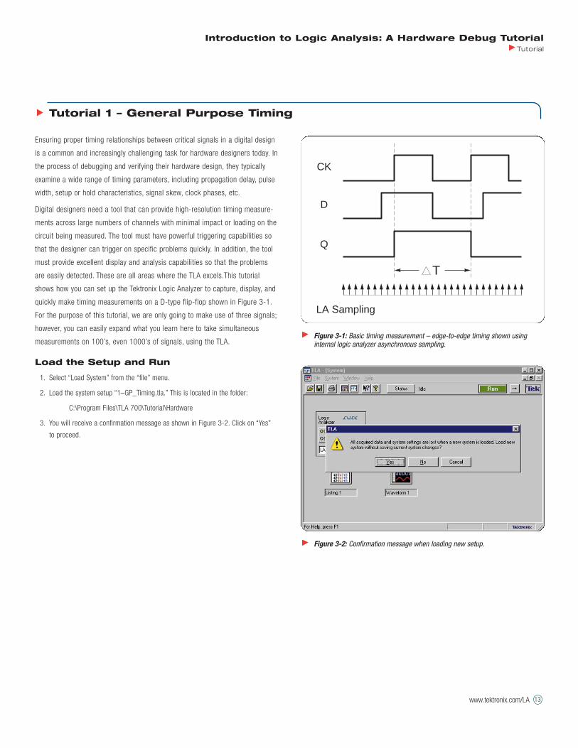
Ensuring proper timing relationships between critical signals in a digital design
is a common and increasingly challenging task for hardware designers today. In
the process of debugging and verifying their hardware design, they typically
examine a wide range of timing parameters, including propagation delay, pulse
width, setup or hold characteristics, signal skew, clock phases, etc.
Digital designers need a tool that can provide high-resolution timing measure-
ments across large numbers of channels with minimal impact or loading on the
circuit being measured. The tool must have powerful triggering capabilities so
that the designer can trigger on specific problems quickly. In addition, the tool
must provide excellent display and analysis capabilities so that the problems
are easily detected. These are all areas where the TLA excels.This tutorial
shows how you can set up the Tektronix Logic Analyzer to capture, display, and
quickly make timing measurements on a D-type flip-flop shown in Figure 3-1.
For the purpose of this tutorial, we are only going to make use of three signals;
however, you can easily expand what you learn here to take simultaneous
measurements on 100’s, even 1000’s of signals, using the TLA.
Load the Setup and Run
1. Select “Load System” from the “file” menu.
2. Load the system setup “1–GP_Timing.tla.” This is located in the folder:
C:\Program Files\TLA 700\Tutorial\Hardware
3. You will receive a confirmation message as shown in Figure 3-2. Click on “Yes”
to proceed.
Introduction to Logic Analysis: A Hardware Debug TutorialTutorial
www.tektronix.com/LA 13
Tutorial 1 – General Purpose Timing
Figure 3-1: Basic timing measurement – edge-to-edge timing shown usinginternal logic analyzer asynchronous sampling.
T
CK
D
Q
LA Sampling
Figure 3-2: Confirmation message when loading new setup.

14
Configuring Your TLA600 to Match Saved Setup
When a setup is loaded on a TLA that is not the same channel width as
the original where the setup was created, there is an additional step
required to properly configure the logic analyzer. Setups created on TLAs
of lower channel count can easily be transferred to logic analyzers of
equal or higher count. All the setups for these tutorials were created on a
34 channel TLA611.
An information window will appear as shown in Figure 3-3 advising you of
this.
4. Click on “OK” to proceed. This will bring up the “Load System Options” dia-
log box as shown in Figure 3-4.
5. Drag the logic analyzer icon from the GP_Timing box to the Current System box.
This will load the saved setup onto the logic analyzer you are using.
6. Click on “OK” to complete loading the saved setup. This will take you to the
System Window shown in Figure 3-5.
7. Click on the “FF Analysis” waveform button (see Figure 3-5). This will take you to
the Data Window.
Tip: Setups can be saved either with or without data. Often it is useful to
capture data and save it along with the setup for future reference or doc-
umentation. In some applications it is also useful to save data in a "refer-
ence memory" and compare known good data to acquired data.
8. Click on the “Run” button to begin acquiring new data. The logic analyzer is set
up to trigger on anything, so it will immediately acquire data and display in the
waveform window as shown in Figure 3-6. The data should look similar but will
not necessarily be the same from acquisition to acquisition.
Introduction to Logic Analysis: A Hardware Debug TutorialTutorial
www.tektronix.com/LA
Figure 3-4: Load System Options dialog window.
Figure 3-3: Information window asking user to use "Load Systems Options" dia-log to configure setup on new logic analyzer.

View the Data and Make a TimingMeasurement
1. Click on the “Run” button a few times to see if the data changes.
2. Use the “Horizontal Position” knob on the front panel to position the data on
screen so that you can see the trigger indicator (“T”) clearly. See Figure 3-6 to
see what the trigger indicator looks like.
Tip: You can also move the data window to the Trigger cursor position by
dragging the slider button in the memory scroll bar or pressing “Cntrl” +
“T.” Try both methods.
3. Place the mouse cursor on the leading (rising) edge of one of the FF-Q signals
and right-click the mouse. Select “Move cursor 1 here” (see Figure 3-7). This will
move the first cursor to this location.
4. Place the mouse cursor on the trailing (falling) edge of the same FF-Q signal.
right-click and select “Move cursor 2 here.” This positions the second cursor.
Introduction to Logic Analysis: A Hardware Debug TutorialTutorial
www.tektronix.com/LA 15
Figure 3-5: Restored system for Tutorial 1.
Figure 3-6: Captured signals from flip-flop showing trigger "T" at start of data.
Figure 3-7: FF-Q pulse width measured.
WaveformButton
TriggerIndicator Memory
Location Bar
Spin ControlBoxes Right-click here and select
“Move cursor 1 here”

16
Tip: To line up the cursors exactly over the signal edge, you can fine tune
the cursor placement by clicking on the cursor spin box controls as
shown in Figure 3-7.
5. By reading the number in the “Delta Time” box, you are measuring the time dif-
ference between the two cursors. In this case, we are measuring the pulse width
of the FF-Q signal. The resolution for this measurement is 10 ns as indicated by
the sample ticks on the display. As you will see later, sample resolution is set in
the Setup window.
Tip: There are several useful key commands available to the user to posi-
tion cursors, move data, take acquisitions, etc. For a quick reference, go
to the “Help Topics” in the Help menu and search on “Shortcut.” There
are several shortcut topics listed. Try exploring a few of these to find use-
ful shortcut keys or control functions.
View the Trigger Setup
1. Click on the “Window” pull-down on the top menu bar and select “Trigger: LA 1.”
The Trigger window that appears should be similar to Figure 3-8.
The Trigger window shows the conditions that the logic analyzer used to detect
and capture the data of interest. In this case, the TLA is set up to trigger on
"Anything," which means that the logic analyzer triggers as soon as the “Run”
button is pushed. Notice that the "Trigger Pos" is set to 0%. With this setting, all
data collected appears after the trigger.
View the Channel Setups
1. Click on the “Window” pull-down menu on the top toolbar and select “Setup: LA
1.”
Figure 3-9 shows the Setup window used in this tutorial. This is where the
channel mappings to our training board were defined and given names.
Notice that the “Clocking:” box is set to “Internal” which means that we are
sampling asynchronously or using the internal logic analyzer clock to acquire
data. If you are unfamiliar with this terminology, please refer to XYZs of Logic
Analyzers.
Introduction to Logic Analysis: A Hardware Debug TutorialTutorial
www.tektronix.com/LA
Figure 3-8: Trigger condition for Tutorial 1.
Figure 3-9: Channel setups for Tutorial 1.

2. Click on the box in the upper right hand corner labeled “Show Activity.” This will
display all the logic analyzer probes and will indicate which ones have active sig-
nals as shown in Figure 3-10. Try removing the C2 probe from the logic analyzer
front panel and observe how the activity arrows behave. When done, close the
dialog box.
Tip: Use the Activity dialog box to see if you have connection and live sig-
nals when setting up your own acquisitions. This function is like having a
logic probe across all of your channels.
3. After viewing the setups, make sure that the C2 probe is reconnected and return
to the System Window.
Note: If you wish to stop at this point and come back to Tutorial 1 at a
later time, select “File” and “Exit” from the main menu bar. Answer “Yes”
to Exit without saving changes. It is now safe to shut down the logic ana-
lyzer.
What You Learned
In this tutorial you learned how to load an existing setup into a TLA, acquire
waveform data, move the cursors, and make basic timing measurement on a D
flip-flop. You also examined the setups and trigger windows to view how the
TLA was setup to capture this data and used the “Show Activity” function to
check for signal activity from the target board.
Congratulations! You have just completed Tutorial 1 – General Purpose Timing
You are now ready to move on to the next section, Tutorial 2 – Glitch
Detection.
Introduction to Logic Analysis: A Hardware Debug TutorialTutorial
www.tektronix.com/LA 17
Figure 3-10: Probe activity window.

18
Introduction to Logic Analysis: A Hardware Debug TutorialTutorial
www.tektronix.com/LA
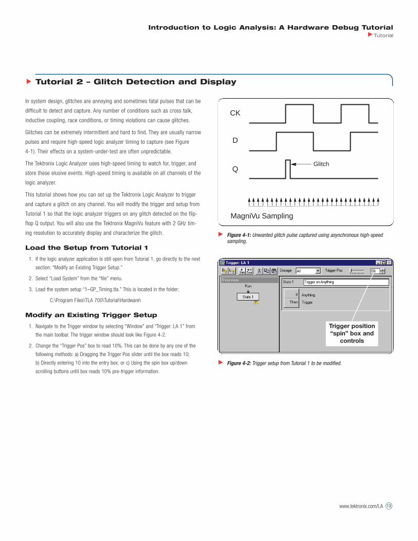
In system design, glitches are annoying and sometimes fatal pulses that can be
difficult to detect and capture. Any number of conditions such as cross talk,
inductive coupling, race conditions, or timing violations can cause glitches.
Glitches can be extremely intermittent and hard to find. They are usually narrow
pulses and require high-speed logic analyzer timing to capture (see Figure
4-1). Their effects on a system-under-test are often unpredictable.
The Tektronix Logic Analyzer uses high-speed timing to watch for, trigger, and
store these elusive events. High-speed timing is available on all channels of the
logic analyzer.
This tutorial shows how you can set up the Tektronix Logic Analyzer to trigger
and capture a glitch on any channel. You will modify the trigger and setup from
Tutorial 1 so that the logic analyzer triggers on any glitch detected on the flip-
flop Q output. You will also use the Tektronix MagniVu feature with 2 GHz tim-
ing resolution to accurately display and characterize the glitch.
Load the Setup from Tutorial 1
1. If the logic analyzer application is still open from Tutorial 1, go directly to the next
section: “Modify an Existing Trigger Setup.”
2. Select “Load System” from the “file” menu.
3. Load the system setup “1–GP_Timing.tla.” This is located in the folder:
C:\Program Files\TLA 700\Tutorial\Hardware\
Modify an Existing Trigger Setup
1. Navigate to the Trigger window by selecting “Window” and “Trigger: LA 1” from
the main toolbar. The trigger window should look like Figure 4-2.
2. Change the “Trigger Pos” box to read 10%. This can be done by any one of the
following methods: a) Dragging the Trigger Pos slider until the box reads 10;
b) Directly entering 10 into the entry box; or c) Using the spin box up/down
scrolling buttons until box reads 10% pre-trigger information.
Introduction to Logic Analysis: A Hardware Debug TutorialTutorial
www.tektronix.com/LA 19
Tutorial 2 – Glitch Detection and Display
Figure 4-1: Unwanted glitch pulse captured using asynchronous high-speedsampling.
MagniVu Sampling
CK
D
QGlitch
Figure 4-2: Trigger setup from Tutorial 1 to be modified.
Trigger position“spin” box and
controls

20
3. Click on the “If-Then” button to view the clause definition for the trigger state.
4. In the “If” pull-down definition box, select “Glitch.” The “Then” pull-down defini-
tion box should still read “Trigger.”
5. Click on the “Define Glitches” button in the upper right corner of the dialog box.
The Glitch Detection dialog box defines which groups of channels the logic ana-
lyzer will look at to find glitches. With the TLA, the user may wish to check for
glitches on a large number of channels or groups at the same time. In this exer-
cise you are only interested in the Q output of the flip-flop, so make sure that
only "FF Q-OUT" is selected. The dialog box should be similar to Figure 4-3.
6. After making sure that “FF Q-OUT” is the only box checked, close the “Glitch
Detection” and “Clause Definition” dialog boxes by clicking on “OK” at the bottom
of each box.
7. In the box to the right of “State 1,” delete “Trigger on Anything” and type in
“Trigger on Glitches.” This provides a useful way to document the trigger condi-
tion.
8. The “Trigger Window” should look like Figure 4-4 when you are finished.
Run
1. Open the waveform data window labeled “FF Analysis” by using the “Window”
pull-down menu at the top of the screen.
2. Click on the “Run” button to begin acquiring data. The logic analyzer will trigger
on the first glitch that it detects on the FF-Q signal and stop. Try clicking on the
“Run” button a few times to see if the data changes.
Tip: Use the “Repetition” button next to “Run” to continuously acquire new
data. Press “Run” when you are ready to “Stop” the acquisition.
View the Data
1 The waveform should look similar to that shown in Figure 4-5. If necessary, use
the “Horizontal Position” knob on the front panel to scroll the data until the “T”
indicator (trigger indicator), is in the center of the screen.
Introduction to Logic Analysis: A Hardware Debug TutorialTutorial
www.tektronix.com/LA
Figure 4-4: Trigger window for for “Trigger on Glitches.”Figure 4-3: Glitch Detection dialog box.

Tip: You can also use “Cntrl” + “T” to move the data window to the trig-
ger position if it is off screen. This method will bring the Trigger indicator
to mid screen which is often the most useful position when zooming in.
The logic analyzer has detected and triggered on a glitch in the vicinity of the
trigger indicator but we cannot see the actual fault. Some logic analyzers have
this ability to trigger on a glitch but very few can indicate what channel it
occurred on and actually capture and display the glitch.
Change the Acquisition Mode to Glitches
1. Open the Setup window by using the “Window” pull-down menu at the top of the
screen and select “Setup: LA 1.”
2. In the “Acquire” pull-down box select “Glitches.” This configures the TLA to
acquire and store glitches on all channels.
3. Go to the waveform window by selecting “FF Analysis” under the “Windows” pull-
down menu.
Run
Click on the “Run” button to begin acquiring data. The logic analyzer will
acquire, trigger, capture, and display glitches.
View the Data
1. You should see a display similar to Figure 4-7. If the cursors one and two are
not on screen, they can be brought into view by dragging the cursor indicators at
the bottom of the waveform window.
Tip: Place your mouse in the waveform area and right-click. Select “Go
To” and “Go To” again. Click on where you want the data to be located. In
the above example, you would select “Cursor 1.”
2. Click on the “Run” button a few times to see if the glitch data changes.
Notice the red area to the left of the trigger indicator. This marking indicates the
presence of a glitch between the trigger sample point and the previous data
sample point. To find out what actually caused these glitches, you will use the
Introduction to Logic Analysis: A Hardware Debug TutorialTutorial
www.tektronix.com/LA 21
Figure 4-5: Glitch detected but not displayed.
Figure 4-6: Changing the Acquisition mode to “Glitches” in the Setup Window.

22
MagniVu feature (500 ps timing resolution) of the Tektronix Logic Analyzer to ana-
lyze the glitch more closely.
Adding High Speed Timing (MagniVu™) tothe Display
In this section, we will show how you can set up the analyzer to store, display,
and measure glitches using MagniVu. This innovative Tektronix feature provides
a 2K buffer of high-speed timing around the trigger point at all times. This
allows the user to zoom in on areas of high interest or probable causes of tim-
ing faults with maximum resolution.
1. Right-click on the open area under the last channel using the right mouse button.
Select “Add Waveform.” This will bring up the Add Waveform dialog box.
2. Select “LA1-MagniVu” in the Data Source pull-down box.
3. Highlight “Sample” under the Group column as shown in Figure 4-9 and click on
the Add button. This will add the MagniVu sample indicator to the Waveform
window.
Introduction to Logic Analysis: A Hardware Debug TutorialTutorial
www.tektronix.com/LA
Figure 4-7: Glitch Indicator.
Figure 4-8: Location to add waveform.
CursorIndicators
Red GlitchIndicator
Right-click inthis area to add
waveform
Figure 4-9: Adding “Sample” to the Waveform window.

4. Refer to Figure 4-10. Select the radio button “By Name.” This will change the
listing in the main display box.
5. Highlight all three rows as shown in Figure 4-10 by using the “Cntrl” key and the
left mouse button. Click on the “Add” button. This will add all of the FF signals
with MagniVu timing to the display. Close the dialog box by selecting “Close.”
Changing the Height of theDisplayed Channels
In the next couple of steps, you will change the height of the MagniVu display
channels to better see the data. Refer to Figure 4-11 for these steps.
1. Highlight the three channel names added in the previous step (far left column) by
using your left mouse button and the “Cntrl” key. Do not highlight the Sample
channel.
2. Using the right mouse button to open a pop-up menu, select “Properties.” In the
Properties dialog box, select the “Waveform” tab and change the “Height’" box to
read 36. Click on “OK” when you are done. The MagniVu channels should now be
the same height as the original timing signals.
Tip: You can also change the height of any channel or selected group of
channels by clicking on them (use “Cntrl” key to select more than one)
and using the “Size” knob on the front panel. The height can also be
changed by dragging the edge of a channel in the left column and
expanding its size.
Tip: Change the color of individual waveforms so that they stand out bet-
ter in the same Properties dialog box.
View the Glitch
1. Notice the greater resolution available with the 2 GHz sampling. The MagniVu
feature provides the ability to make measurements with 500 ps resolution. The
glitch in Figure 4-12 now appears as a single narrow pulse. The glitch only
became visible using the MagniVu feature with 2 GHz sampling.
2. Look at the relationship of other channels using the MagniVu feature to make
some deductions about the events that caused the glitch. The glitch is a pulse
Introduction to Logic Analysis: A Hardware Debug TutorialTutorial
www.tektronix.com/LA 23
Figure 4-10: Add Waveform dialog box.
Figure 4-11: Changing the height of displayed channels.

24
that appeared between two adjacent samples (these pulses are often missed by
basic logic analyzers).
Measure Glitch Pulse Width
The next steps show how to measure the pulse width of the captured glitch
using the cursors in the Waveform window:
1. Click on the “Zoom In” button (under the “Run” button) until the Time/Div reads
2ns.
You can also use the front-panel horizontal “SCALE” knob of the logic analyzer to
zoom in on the pulse. You may have to adjust the trace horizontally using the
Horizontal “POSITION” control knob on the front panel or by using the scroll but-
ton on the bottom of the waveform window to center the glitch pulse.
2. Move the mouse pointer to the leading (rising) edge of the glitch pulse (on the
Mag_FF-Q channel). Right-click the mouse and select “Move Cursor 1 Here.”
Cursor 1 will be placed at the position of the pointer.
3. Move the mouse pointer to the trailing (falling) edge of the glitch pulse. Right-
click the mouse and select “Move Cursor 2 Here.”
4. Determine the actual pulse width by reading the “Delta Time” readout at the top
of the display. Your screen should look similar to, but not exactly like, Figure
4-13. Note that the glitch may vary in width depending on the acquisition. You
may wish to take several acquisitions to determine the range.
Tip: Use the procedure in the above steps to move the cursors from any-
where outside the displayed information in the window to the mouse posi-
tion. This saves time by not having to scroll through the data to find the
cursors. You can also use “Cntrl” + “1” and “Cntrl” + “2” to move the
cursors to the middle of the screen.
Introduction to Logic Analysis: A Hardware Debug TutorialTutorial
www.tektronix.com/LA
Figure 4-12: Waveform display showing the glitch using MagniVu feature.
Figure 4-13: Glitch pulse width measurement.

Document the Glitch
Often, it is useful or necessary to document your results. The following steps
show how to draw a box around the point of interest and copy a bitmap to
WordPad.
1. Set the Time/Div: to 5ns using the pull-down menu or the “SCALE” control knob.
2. If necessary, center the data so the trigger indicator and the glitch are approxi-
mately at center screen.
3. Click on your left mouse key and drag the cursor around the area of interest. In
this case, drag it around the glitch and the leading edges of the FF-CLK and FF-D
signals. This will create a dotted-line rectangle as shown in Figure 4-14.
4. Right-click within the rectangle that you created and select “Copy Bitmap.” This
will copy a bitmap of the information inside the box to the clipboard.
5. Open WordPad from the Microsoft Windows® Start/Programs/Accessories menu.
6. Right-click your mouse inside the WordPad document and select “Paste.” This
will place a bitmap image of what you had enclosed in the box from the TLA tim-
ing window.
Copy and Paste Entire Screen
If you would like to capture the entire screen, use the “Print Screen” key on
your keyboard or the “Prt Sys” key on the TLA600 front panel. This will place a
bitmap of the whole screen onto the clipboard. Pressing “Alt” + “Print Screen”
will capture the application (TLA application screen). You can use the “Paste”
command or “Cntrl” + “V” to paste the information to Wordpad. This process
will work with any Microsoft Windows word processor or graphics program.
Note: The TLA700 does not have a “Prt Sys” key on the front panel. Use
the keyboard to perform the above functions.
Printer drivers can be installed on the TLA just like any other PC. If you do not
have the printer installation disk or CD-ROM that you wish to connect to, it is
often possible to search the manufacturer’s website and download the latest
printer driver.
Save Your Glitch Setup
At this point, it is useful to save your setup in case you wish to use it again or
recall the setup for further modification to fit your own application.
1. On the top “Windows” menu bar, select “File” and “Save System As.” In the
Setups folder, select the radio button next to “Save all Acquired Data.” This will
save the current setup along with the data acquired.
2. Under C:\My Documents\User save the file as <yourname_glitch>. If this folder
does not exist, create it using the New folder command.
3. Return to the main System Window.
Note: If you wish to proceed at a later time, you can leave the application
by going to the “File” menu and selecting “Exit.”
Introduction to Logic Analysis: A Hardware Debug TutorialTutorial
www.tektronix.com/LA 25
Figure 4-14: Creating a bitmap of selected area on data window.

26
What You Learned
In this tutorial, you learned that glitches can be very disruptive to proper circuit
operation and are very hard to detect, especially across a large number of
channels. You learned how to modify an existing setup so that the logic ana-
lyzer would trigger on a glitch. By enabling glitch storage, and using MagniVu
high-speed timing, you were able to capture and display the glitch and were
also able to measure its width with the TLA cursors. You also copied a bitmap
of the glitch to a word processor for documentation. Finally, you saved your
setup for further use.
Congratulations! You have just completed Tutorial 2 – Glitch Detection and
Display. You are now ready to begin Tutorial 3 – Capture a Setup or Hold
Violation where you will learn how to detect a common cause of glitches.
Introduction to Logic Analysis: A Hardware Debug TutorialTutorial
www.tektronix.com/LA

Setup or hold violations can be difficult to detect and capture, even with a
high-speed logic analyzer. It may even be impossible to detect the violations
with a high-channel count, general-purpose logic analyzer. With the Tektronix
Logic Analyzer and MagniVu, capturing setup or hold violations becomes an
easy task. Once the designer has determined which signal is faulty using the
logic analyzer, he can analyze the circuit further to determine the cause.
Setup time is defined as the minimum time that data must be valid and stable
prior to the clock edge (see Figure 5-1). Hold time is the minimum time that
data must be valid and stable after the clock edge occurs. The manufacturer
specifies these parameters and digital designers take great care to ensure that
their designs do not violate the specifications. Despite these efforts, with
today’s tighter tolerances and tendency to use faster parts and drive more
throughput, setup or hold violations are common faults. These violations may
cause the device output to become unstable (metastability) and perhaps cause
unexpected glitches or signals. Setup or hold violations are one of the causes
of glitches. Once detected, the designer needs to closely examine the circuit to
determine if any design rules are being violated that result in setup or hold vio-
lations.
In the following tutorial, you will use a pre-defined setup to capture setup or
hold violations on a D flip-flop. Unlike the previous two tutorials where you
acquired the data asynchronously using the internal logic analyzer clock to
acquire the sample, you will be using the clock signal from the QuickStart
Training Board to acquire data. This is referred to as synchronous acquisition. If
you are unfamiliar with any concepts, the XYZs of Logic Analyzers from
Tektronix is an introductory primer to the fundamentals of logic analysis.
You will be using MagniVu channels to view the data with the highest possible
timing resolution since setup or hold times are specified with 500 ps resolu-
tion. For this tutorial, we have constructed a data window that only includes
MagniVu channels. It should be noted that the MagniVu feature is always avail-
able and provides a 2K buffer of 2GS/sec data around the trigger point. Since
you will be triggering on a setup or hold violation, the MagniVu feature can give
you the best possible timing resolution around the violation.
Load the Setup and Run
1. On the top Windows toolbar, select “File” and “Load System.”
2. Load the saved setup “3-Setup_Hold.tla.” This is located in the folder:
C:\Program Files\TLA 700\Tutorial\Hardware\
3. From the top Windows toolbar select “Windows” and “MAG_FF–Anlys.”
Introduction to Logic Analysis: A Hardware Debug TutorialTutorial
www.tektronix.com/LA 27
Tutorial 3 – Capture a Setup or Hold Violation
Figure 5-1: Setup or Hold parameters – synchronous acquisition using externalclock from circuit-under-test.
Hold
Setup
MagniVu Sampling
EXTCK
D
Q

28
4. Maximize the waveform window (if not maximized already).
5. Click on the “Run” button to begin acquiring data.
6. Center the Trigger indicator on the screen by pressing “Cntrl” + “T” (if required).
7. Take several acquisitions to see how the data changes. You will notice that the
logic analyzer will detect several different setup or hold violations on the FF-D
input signal. When you get an acquisition that looks similar to the one in Figure
5-2, stop and proceed to the next section.
View the Resultant Data
1. Measure the setup or hold times nearest the trigger mark (measure from the ris-
ing edge of the clock to the data transition of the FF-D channel). If necessary,
refer to Tutorial 1 and 2 for moving cursors.
Tip: If the cursors are already on screen, you can easily drag them to
position by grabbing the cursor handles above the waveform window
using your mouse with the left button depressed.
Notice the excellent (500 ps) resolution available with the MagniVu feature using
the 2 GHz sampling. The waveform display should look similar to Figure 5-2.
2. Click on the “Run” button several times to see how the timing violation varies
with each data acquisition.
The logic analyzer actually evaluates every rising edge of the clock for a setup or
hold violation. While the logic analyzer monitors millions of events, it captures
only those that fail the setup or hold requirements. In the example shown in
Figure 5-2, the setup time was only 1.48 ns, which is less than the limit of
2.5 ns.
View the Trigger Setup
To understand how the logic analyzer captured the setup or hold violation, view
the setups in the Trigger window.
1. From the Windows pull-down menu on the top toolbar select “Trigger: LA1.”
2. Click on the “If-Then” button to view the clause definition. The “If” clause is set to
“S & H fault.”
3. Click on the “Define Violation” button to open the dialog box.
The dialog box lets you define the setup or hold parameters for the channels. The
designer will typically use the setup or hold specifications listed in the manufac-
Introduction to Logic Analysis: A Hardware Debug TutorialTutorial
www.tektronix.com/LA
Figure 5-2: Timing waveform display for Tutorial 3.
Figure 5-3: Define Violation dialog box for Tutorial 3.

turer’s data sheet for the part being monitored. For our flip-flop, the setup speci-
fication is listed at 2.5 ns at room temperature.
The dialog box should be similar to Figure 5-3. If you wish to see the effects of
changing the setup or hold parameters on your acquisition, you can try changing
the values and testing the results by taking further acquisitions.
4. Close the open dialog boxes by clicking on “Cancel” in each case.
5. Select Windows pull-down menu from the top toolbar and click on “Setup: LA1.”
Note that the Clocking: pull-down box is set up to use the clock from the
QuickStart board as the “External” clock source. To trigger on a setup or hold vio-
lation, use External clocking.
6. Click on the “More…” button to view the “Clocking” dialog box. You can see that
“CK3” is the selected clock, which is physically connected to the clock “CNTR-
CLK” from header J760 on our QuickStart training board. It is set to acquire
using a positive going edge. Your display should look similar to Figure 5-4.
7. After viewing the Setup Window, close the Clock Definition dialog box and return
to the System Window. You are now ready to proceed to the next Tutorial.
What You Learned
In this tutorial, you successfully learned how to capture and analyze a setup or
hold violation, which is a common cause of glitches and missed signals in digi-
tal designs. You also learned how to change the TLA to synchronous acquisi-
tion, so that sampling is controlled by a clock from the circuit-under-test. By
using the MagniVu feature high-speed timing, you were able to measure the
setup violation with 500 ps resolution.
Congratulations! You have just completed Tutorial 3 – Capture a setup or hold
Violation. You are now ready to proceed to the next section, Tutorial 4 –
Transitional Storage.
Introduction to Logic Analysis: A Hardware Debug TutorialTutorial
www.tektronix.com/LA 29
Figure 5-4: Setup window for Setup or Hold Tutorial showing Clock Definitiondialog box.

30
Introduction to Logic Analysis: A Hardware Debug TutorialTutorial
www.tektronix.com/LA

There are times when you need to capture a series of events that are sepa-
rated by wide time intervals of inactivity. An example of this is widely separated
data bursts feeding a D/A converter in a radar system or some other communi-
cations system bus where the data is “bursty” in nature. Using “store all,”
sometimes referred to as conventional storage, the logic analyzer quickly fills
its acquisition memory with non-changing data thereby limiting the time span
of acquired data. What's needed is a method whereby the logic analyzer stores
data only when there is a transition. This is called transitional storage.
With transitional storage as shown in Figure 6-1, the logic analyzer only sam-
ples when the data changes. Events that are seconds, minutes, hours, or even
days apart are captured with 4 ns timing resolution.
In this exercise, you will setup the TLA to capture a repetitive signal consisting
of four groups of eight 16 to 24 ns pulses separated by 1.3 ms of inactivity
using both conventional and transitional storage techniques and see the differ-
ence in effective overall time window.
Load the Setup for ConventionalTiming and Run
1. On the top Windows toolbar, select “File” and “Load System.”
2. Load the saved setup “4-Storage_All.tla.” This is located in the folder:
C:\Program Files\TLA 700\Tutorial\Hardware\
3. From the top Windows pull-down menu toolbar select “Windows” and “Burst.”
4. Click on the “Run” button to begin acquiring data.
View the Resultant Data
1. Adjust the position of the waveform on the screen until you see the bursts shown
in Figure 6-2. Try using the Horizontal Position knob on the front panel of the
logic analyzer to scroll the data to the end of the waveform (to the right of the
screen).
Introduction to Logic Analysis: A Hardware Debug TutorialTutorial
www.tektronix.com/LA 31
Tutorial 4 – Transitional Storage
Figure 6-2: Burst data captured using Conventional Storage.
Figure 6-1: Transitional sampling – acquisition taken on each change in dataonly.
Sample Stored on Transition
BurstData

32
You will see four groups of eight pulses following the trigger. You will not see any
more sets of pulses on the display; however, the next set of four data bursts
occur approximately 1.31 ms later with no signal activity in between. Since we
are using 1K memory depth in our setup (you can view the “Setup Window”), we
can only see the first burst of four groups of pulses. With 1K of memory depth,
we don't see the next burst, which we suspect to be 1.3 ms away.
2. Place your cursor on any unused part of the data display window (dark back-
ground area) and right-click on the mouse. Select “Zoom” and “All.” This will
compress the whole acquisition memory window onto the screen.
Notice how the memory slider at the bottom of the window now fills up the whole
bar and that the overall time window is only slightly over 4 µs.
There is clearly not enough memory depth to capture the second burst of data.
We would need at least 325 times more memory depth using conventional mem-
ory (1.31 ms/4 ns x 1K = 325K memory depth).
Observe that there is a tremendous amount of unchanging data being stored;
i.e., all zeros. What if we could only store when data transitioned, thereby widen-
ing our time window to see the next data burst, yet maintain the 4 ns timing res-
olution?
Tip: You can also use the “SCALE” knob on the front panel to change the
timebase and show the full acquisition on screen.
Modify the Trigger for Transitional Timing
1. Select “Trigger: LA1” from the Window pull-down menu.
2. In the Storage pull-down box, change the mode from “All” to “Transitional.”
Notice that a new “If-Then” clause is added to the window.
3. If you click on the “Change Detect” button, the “Burst” box should be checked.
4. Verify that your settings match those in Figure 6-3. Click on “OK” to exit the
“Change Detection” box. The TLA is now set to trigger on the first data burst of
the Burst signal with transitional storage enabled.
Run and View the Acquired Data UsingTransitional Storage
1. Open the waveform window labeled “Burst,” from the Windows pull-down menu
and ensure that it is maximized. This should still contain data from the last acqui-
sition.
2. Press “Run.” You should now see the same four bursts of pulses; however, the
memory indicator in the scroll bar at the bottom of the window is now much
smaller, indicating that we have acquired data over a much greater time span.
3. Right-click the mouse button in the dark area under the burst signals and select
“Zoom” and “All.” This will show the entire acquisition compressed into the win-
dow. Notice that we are looking at a time span of over 19 ms with several bursts
displayed. Your display should now look like Figure 6-4.
Notice that instead of one burst (four groups of eight pulses), the memory is filled
with 16 bursts. The time window went from ~4.1 µs to 19.7 ms. For the Burst
Introduction to Logic Analysis: A Hardware Debug TutorialTutorial
www.tektronix.com/LA
Figure 6-3: Trigger window setup for Transitional storage Tutorial 4.

signal, this represents an overall time window that is almost 4,800 times greater
using transitional storage compared to conventional storage (store all).
If you examine the sample indicator you will also note that sample acquisitions
are not taken during the “dead time” between bursts. This optimizes acquisition
memory by only taking samples when there is a change in the data.
4. Right-click in the same area as was done in step 3 and select “Zoom” and
“Previous.” This will take you back to the original waveform view. You may also
try using the “SCALE” knob on the front panel to accomplish the same task.
Save Your Transitional Timing Setup
If you would like to save your setup for future reference, perform the following
steps:
1. Select “Save System As…” under the Windows “File” pull-down menu.
2. Check off the radio button “Save all Acquired Data” under Save Options. This will
save the data that you collected along with the setup.
3. Save the file as <yourname_transitional> in:
C:\My Documents\User
Pre-configured Transitional Timing Setup
If you would like to explore a pre-saved setup for transitional timing, you can
perform the following steps.
1. Load the saved setup “4-Storage_Transitional.tla.” This is located in the folder:
C:\Program Files\TLA 700\Tutorial\Hardware\
What You Learned
In this tutorial, you have learned how to optimize the logic analyzer acquisition
by using transitional storage. The logic analyzer only takes an acquisition when
the data changes. By using this feature, you can capture widely spaced or
“bursty” data. Transitional storage can help you optimize the memory depth
that you currently have on your logic analyzer.
Congratulations! You have just completed Tutorial 4 – Transitional Storage.
You are now ready to proceed to Tutorial 5 – How to Create and Save Setups.
Introduction to Logic Analysis: A Hardware Debug TutorialTutorial
www.tektronix.com/LA 33
Figure 6-4: Timing waveform using Transitional storage showing widely spacedburst signals.
Multiple data bursts capturedwith 19.6 ms window
MemoryScrollbar Full

34
Introduction to Logic Analysis: A Hardware Debug TutorialTutorial
www.tektronix.com/LA

Before using the logic analyzer to capture signals from your own application, it
is important to know how to create and save a setup. Designers often keep a
library of setups that can be used directly or with some modification for other
similar applications. This saves much time and effort over creating setups for
each application.
This exercise will familiarize you with this procedure by creating the setup that
is used in Tutorial 1. We will also add a separate MagniVu feature waveform-
timing window. In Tutorial 2, we simply loaded the setup and learned how to
modify it for another application. Once you have these basics, you are ready to
start making setups specific to your own applications.
Load the Default Setup
Before creating a new setup it is a good idea to start from a known reference
point. The easiest way to start from a known reference point is to start from the
default setup.
1. Select “Default System” from the “file” menu. The logic analyzer will load a
default setup and display the screen shown in Fig 7-1.
Delete Default Data Windows
1. Right click your mouse on the “Listing 1” data window and select “Delete.”
2. Repeat this process for the “Waveform 1” data window. We will be creating our
own data window later in this tutorial.
Define the Setup Window
After you have set the logic analyzer to the default setup, you need to define
which channel groups and probe channels you will be using. In this tutorial you
will delete any unused channel groups and define the ones you use with the C2
probe.
1 Click on the “Setup” button on the logic analyzer Icon to open the Setup Window.
Alternately you could click on the Windows pull-down menu at the top of the
screen and select the “Setup: LA1” window.
Perform the following steps to delete unused default channel groups:
2. Right-click on any one of the channel groups under the Group Name column (see
Fig 7-2).
3. Select “Delete All Groups” from the menu. This will remove all of the default
groups.
Define New Channels and Groups
This will assign channels on the logic analyzer to the actual physical connec-
tions on the training board. You can rename any of the probe or clock channels
to help display information. This makes it easier to relate individual channel
Introduction to Logic Analysis: A Hardware Debug TutorialTutorial
www.tektronix.com/LA 35
Tutorial 5 – How to Create Setups
Figure 7-1: Default System Screen.

36
names to the signals on the system-under-test. You will also assign the chan-
nels to “Groups.” A “Group” may consist of any number of channels including
only one. All channels, including single channels, must be assigned to a group.
This feature is most commonly used to group together signals on data,
address, and control busses.
In the following steps, channel names are assigned first and groups are cre-
ated second. This order can be reversed if desired. The following also assumes
that you are using the P6418 probe directly connected to header J860 and
CK3 connected to J760.
The physical mappings on the training board for the flip-flop that we will be
examining are shown in Table 7-1.
Refer to the completed “Setup” window in Figure 7-3 to help you with the fol-
lowing steps.
1. In the lower half of the Setup window, select the empty probe C2, channel 5
field and enter the name FF-Q. This assigns channel 5 to the Q output of the flip-
flop.
2. Select the empty probe C2, channel 7 field and enter the name FF-D. This
assigns channel 7 to the D input of the flip-flop.
3. Select the empty CK3 clock field and enter FF-CLK. This assigns the clock chan-
nel CK3 to the clock signal of the flip-flop.
Note: Although it is useful to assign target signal names to channels for
better recognition, it is not mandatory. If no signal name is entered, the
logic analyzer will use the default channel number when it is assigned to
a group.
Introduction to Logic Analysis: A Hardware Debug TutorialTutorial
www.tektronix.com/LA
Figure 7-2: Delete default groups.
Deletegroups here
Figure 7-3: Setup window for Tutorial 5.
Click button to left ofchannel to assign to group
Table 7-1. Physical Mapping of Flip-Flop onTraining Board
Signal Pins on PCB Connections on TLA
D J860 pins 7,8 7
Q J860 pins 5,6 5
CLK J760 pin 1 CK3

Assign Channels to Groups
Now that you have identified the individual probe channels, you must assign
the channels to a channel group. In this case, we will be creating three groups,
each with one channel. Multiple related signals such as address and data
busses are often grouped together. The resultant waveform display of a “Group”
of more than one signal is a composite and known as a “Busform.” The user
can view the busform or open it up to look at the individual channels. For high
channel count acquisitions, this conserves display space and keeps the user
from being swamped with detail until it is needed. It also allows the data on
these buses to be displayed in the Listing Waveform in radix format (binary,
octal, hex, etc.)
1. Click on the top “Group Name” field and enter the name FF CLOCK. Now click on
the box to the left of the FF-CLK field under “CK3.” An X appears indicating that
the FF-CLK channel is assigned to the FF CLOCK group.
2. Click on the next Group Name field and enter the name FF DATA-IN. Now assign
the FF-D channel to the FF DATA-IN group by clicking the box to the left of FF-D.
3. Click on the next Group Name field and enter the name FF Q-OUT. Now assign
the FF-Q channel to the FF Q-OUT group.
Multiple channels can easily be added to a group by clicking on more than one
channel for a given group. This works very well for address and data buses.
Tip: If all of the channels on a given probe are to belong to the same
group, the button to the left of the probe name in the Probe column can
be clicked to assign all the channels from that probe to a group selected
under “Group Name.”
Channels marked by an “X” belong to the currently selected group. Those chan-
nels marked by a “•” belong to other groups not currently selected.
Complete the Setup Window
1. To complete the changes to the Setup window, set the following fields to the val-
ues shown in Table 7-2.
2. Return to the System Window using the “System” icon in the main menu bar.
Define the Trigger Window
After you have defined the channel groups, you can define the trigger parame-
ters. Refer to Figures 7-4 and 7-5 for these steps.
1. In the System Window, click on the “Trig” button to open the Trigger window.
Alternatively click on the Window pull-down menu at the top of the screen and
select the “Trigger: LA1” window.
2. Set the Storage field to “All;” the logic analyzer will store all data samples.
Introduction to Logic Analysis: A Hardware Debug TutorialTutorial
www.tektronix.com/LA 37
Figure 7-4: Trigger Clause Definition dialog box.
Table 7-2. Parameters for Setup Window
Field Value
Clocking Internal, 10 ns
Memory Depth 1024
Acquire Normal
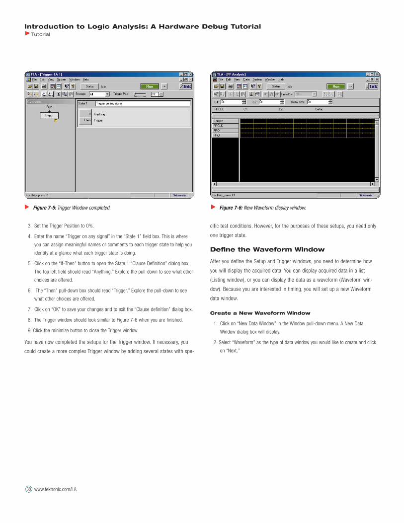
38
3. Set the Trigger Position to 0%.
4. Enter the name “Trigger on any signal” in the “State 1” field box. This is where
you can assign meaningful names or comments to each trigger state to help you
identify at a glance what each trigger state is doing.
5. Click on the “If-Then” button to open the State 1 “Clause Definition” dialog box.
The top left field should read “Anything.” Explore the pull-down to see what other
choices are offered.
6. The “Then” pull-down box should read “Trigger.” Explore the pull-down to see
what other choices are offered.
7. Click on “OK” to save your changes and to exit the “Clause definition” dialog box.
8. The Trigger window should look similar to Figure 7-6 when you are finished.
9. Click the minimize button to close the Trigger window.
You have now completed the setups for the Trigger window. If necessary, you
could create a more complex Trigger window by adding several states with spe-
cific test conditions. However, for the purposes of these setups, you need only
one trigger state.
Define the Waveform Window
After you define the Setup and Trigger windows, you need to determine how
you will display the acquired data. You can display acquired data in a list
(Listing window), or you can display the data as a waveform (Waveform win-
dow). Because you are interested in timing, you will set up a new Waveform
data window.
Create a New Waveform Window
1. Click on “New Data Window” in the Window pull-down menu. A New Data
Window dialog box will display.
2. Select “Waveform” as the type of data window you would like to create and click
on “Next.”
Introduction to Logic Analysis: A Hardware Debug TutorialTutorial
www.tektronix.com/LA
Figure 7-5: Trigger Window completed. Figure 7-6: New Waveform display window.
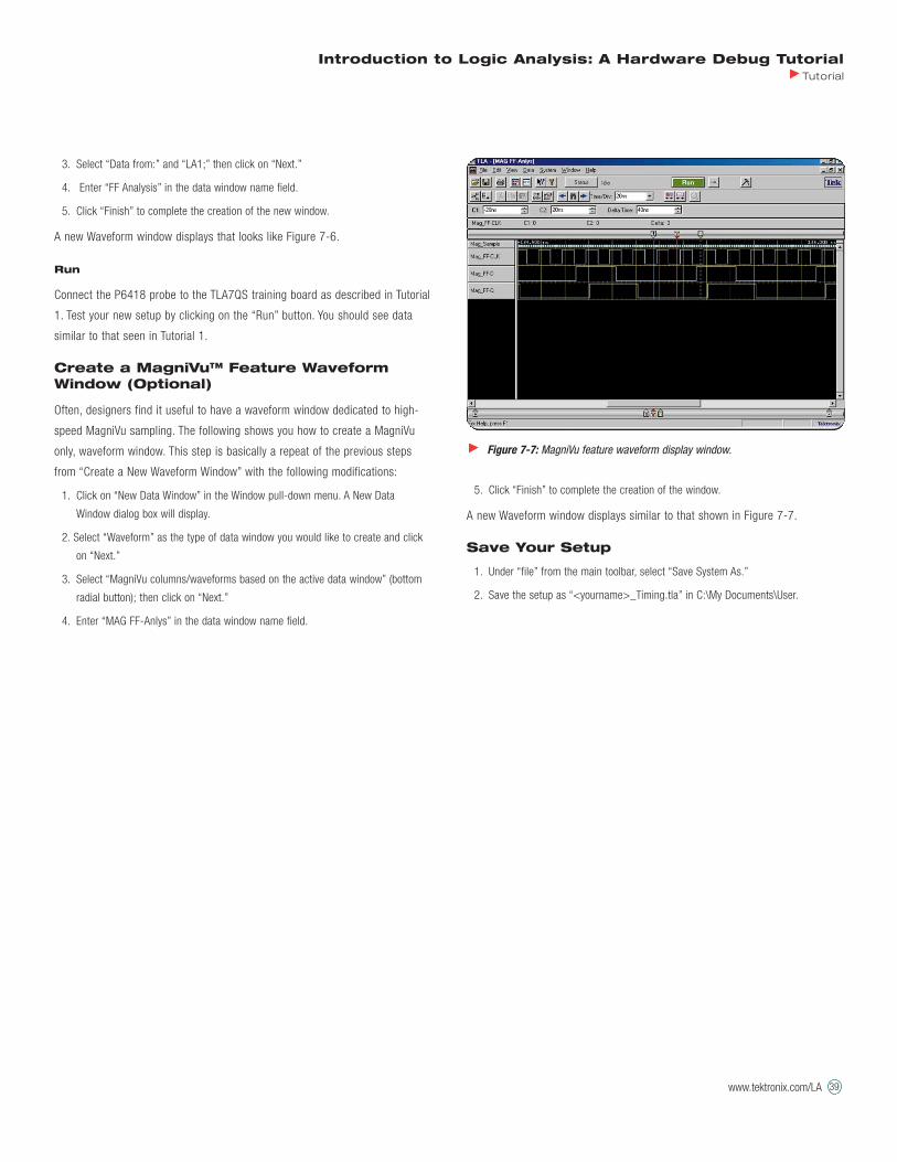
3. Select “Data from:” and “LA1;” then click on “Next.”
4. Enter “FF Analysis” in the data window name field.
5. Click “Finish” to complete the creation of the new window.
A new Waveform window displays that looks like Figure 7-6.
Run
Connect the P6418 probe to the TLA7QS training board as described in Tutorial
1. Test your new setup by clicking on the “Run” button. You should see data
similar to that seen in Tutorial 1.
Create a MagniVu™ Feature WaveformWindow (Optional)
Often, designers find it useful to have a waveform window dedicated to high-
speed MagniVu sampling. The following shows you how to create a MagniVu
only, waveform window. This step is basically a repeat of the previous steps
from “Create a New Waveform Window” with the following modifications:
1. Click on “New Data Window” in the Window pull-down menu. A New Data
Window dialog box will display.
2. Select “Waveform” as the type of data window you would like to create and click
on “Next.”
3. Select “MagniVu columns/waveforms based on the active data window” (bottom
radial button); then click on “Next.”
4. Enter “MAG FF-Anlys” in the data window name field.
5. Click “Finish” to complete the creation of the window.
A new Waveform window displays similar to that shown in Figure 7-7.
Save Your Setup
1. Under “file” from the main toolbar, select “Save System As.”
2. Save the setup as “<yourname>_Timing.tla” in C:\My Documents\User.
Introduction to Logic Analysis: A Hardware Debug TutorialTutorial
www.tektronix.com/LA 39
Figure 7-7: MagniVu feature waveform display window.
40
What You Learned
In this tutorial, you have learned how to create your own TLA setup, including
adding a MagniVu only data window for viewing data with 500 ps resolution.
With this knowledge, you can begin creating and modifying setups for your own
applications.
Congratulations! You have now successfully completed the five tutorials in this
booklet. If you would like to explore the TLA further using your own PC, you can
install an offline TLA viewer called TLAVu which is included on the CD-ROM
that came with this Tutorial package. If you would like further information on
other resources that Tektronix can provide to you, please check the next sec-
tion in this booklet, Resources for You.
Introduction to Logic Analysis: A Hardware Debug TutorialTutorial
www.tektronix.com/LA

If you wish to explore the TLA Family of Logic Analyzers further, this section will
provide you with directions to a number of useful information sources and con-
tact information. Instructions on loading the offline viewer TLAVu onto your PC
are also included here.
Tektronix Logic Analyzers on the Web
Tektronix home page: http://www.tektronix.com
Logic analyzers: http://www.tektronix.com/LA
Product information and data sheets
Processor and bus supports
Application notes, technical briefs
Software drivers and downloads
Press releases, articles
Manuals
Worldwide sales and
service offices: http://www.tek.com/Measurement/wheretobuy/
Technical Support
If you have technical questions with regards to this tutorial, the TLA, or any
other Tektronix product, you can contact your local sales office or our central
Technical Support Center in Beaverton, Oregon, USA. A complete listing of
worldwide country sales and support offices can be found in the Tektronix cata-
log or on the worldwide web.
Tektronix' expert Application Engineers provide technical support on:
Applications
Product operation
Measurement specifications
Hardware and software
Email Support: Send email to [email protected]
24 hours a day, 7 days a week.
XYZs of Logic Analyzers
The XYZs of Logic Analyzers is a primer for hardware or software engineers
who have had little or no experience using logic analyzers and who need to
understand basic concepts and terminology. A printed and bound version can
be ordered online at http://www.tektronix.com/TLA. Simply register and get a
free printed copy sent to your attention.
Introduction to Logic Analysis: A Hardware Debug TutorialTutorial
www.tektronix.com/LA 41
Resources for You
42
QuickStart Training Manual
The TLA7QS QuickStart Training Manual is a full collection of lab exercises that
you can perform using the TLA7QS training board used in this tutorial. Besides
an expanded set of timing and state exercises, this manual explores both soft-
ware trace and pattern generation. The lab exercises are designed to familiar-
ize the user with state listings, disassembly, source code correlation, analysis,
triggering, and pattern generation using live hands-on acquisitions.
The training package can be ordered through your local sales office using the
following description and order number:
QuickStart Training Package: TLA7QS
Training manual
Training board
CD-ROM
You will need to have access to a TLA logic analyzer with appropriate probes.
Your local account manager or application engineer can advise what is required
and assist in helping to get you started.
Tutorial CD-ROM
The CD-ROM provided with this tutorial, contains the following:
Tutorial setup files
Product data sheets
Selected application notes and technical briefs
TLAVu offline viewer (self installing)
In order to view the literature files, you will need Adobe Acrobat reader installed
on your computer.
TLAVu
TLAVu is an offline PC viewer for the TLA Family of logic analyzers. This tool
can be used to view data, create setups, and analyze data previously captured
on a TLA logic analyzer. A copy of TLAVu is included on the tutorial CD-ROM so
that you can install it on a PC. With TLAVu, you can review the setups and data
from the tutorial without the logic analyzer. We have also included other setups
with data so that you can see how the TLA works in a wide range of applica-
tions.
TLAVu is compatible with Windows 95, Windows 98, Windows NT 4.0, and
Windows 2000 and requires that you install it on the C: drive of your PC. See
the Appendix for installation instructions.
Introduction to Logic Analysis: A Hardware Debug TutorialTutorial
www.tektronix.com/LA

Installation of TLAVu on a PC
Because the TLA application software is always located on the C: drive on the
TLA, it is necessary that TLAVu also be installed on the C: drive of your PC. The
TLAVu install program does not allow you to specify where it gets installed. The
main requirement is that your Program Files directory needs to be on the C:
drive.
TLAVu occupies about 25M of disk space once installed and requires about two
times that amount temporarily to perform the install. The install program
checks for adequate disk space before starting the install. In some circum-
stances you may need to restart Windows after installing TLAVu; the TLAVu
install program will inform you if this is the case. An uninstall program is pro-
vided with TLAVu and is accessed through the Add/Remove Programs applet of
the Windows Control Panel.
1. Load the tutorial CD-ROM. From the Start menu on your Windows desktop, select
“Run.” Type in the following:
<Drive>:\TLAVu\Tlavuxx.exe
• XX represents the version of TLAVu on the CD-ROM
• For example, if the version number is 4.0, the file will read Tlavu40.exe
TLAVuXX.exe will unpack itself and create a folder called TLAVuXX (XX will refer
to the version number) under Program Files.
2. Using Windows Explorer or the “Run” command from the Start menu on your PC,
go to the following folder and run “Setup.exe:”
C:\Program Files\TLAVuXX\TLAVu\Setup.exe
Once the installation is complete, you are ready to begin using TLAVu to look at
the setups used for these tutorials, the setups with data that you created, as
well as other sample acquisitions.
Viewing Data
Here are the major ways to use TLAVu to view previously acquired TLA acquisi-
tion data. These are:
a) Load System
b) New Data Window
c) Load Data Window
Load System
The Load System operation loads the previously saved system into TLAVu. This
operation actually changes the configuration of TLAVu to match that of the
saved system. All of the modules, acquisition data, and data windows in the
saved system are loaded into TLAVu.
1. Click on the “TLA Application” icon on your desktop. This will open the TLAVu
application.
When the viewer is finished loading, you will see the same default System
Window from the Tutorials.
2. From the main menu bar, select “File” and “Load System.” Navigate to the follow-
ing folders on your Tutorial CD-ROM and load the following file:
<Drivename>:\Tutorial\Hardware\Samples\SampleSystemData.tla
This will load a setup with previously captured data from an 8-bit down counter.
Select the Waveform window (8 bit dw-cnt) and observe the “busform” data. This
was mentioned in Tutorial 1 as a way to group related channels to conserve dis-
play space. The individual channels can be viewed by right clicking on any chan-
nel group and expanding the channels.
3. Right click your mouse on the top channel group, “"LA: Down Count” and select
“Expand Channels.” You will now see that this group was composed of eight sep-
arate data channels.
Introduction to Logic Analysis: A Hardware Debug TutorialTutorial
www.tektronix.com/LA 43
Appendix

44
4. Right click your mouse on any one of the channels and select “Collapse
Channels.” This will restore the busform.
5. Try loading other setups from the same folder. Some of the setups include listing
windows and other data views that, although not covered in this tutorial, are indi-
cations of the full capabilities of the TLA.
You can also examine the setup files from the tutorial. These were saved with
actual data and are located on the Tutorial CD-ROM, in the following folder:
<Drivename>:\Tutorial\Hardware\Setups\*.tla
Try loading these files and examining the saved data. You can move your cur-
sors, scroll through the data, and even copy screen images to other documents
as bitmaps.
New Data Window
The New Data Window operation creates a completely new data window. You
can either create a data window that initially has no data in it and then incre-
mentally add waveforms or columns of data, or you can create a new data win-
dow and specify your previously saved data as the data source. In either case,
you will at some point in the process need to press a button named “Add Data
Source…” This is where you specify the file that contains the saved data. This
method of viewing saved data (New Data Window) will work with a file that was
created by either the Save Module or the Save System operation on the TLA.
Load Data Window
The Load Data Window operation loads a previously saved data window. This
will only work if the file containing the saved data was created on the TLA
using the Save System operation. This is because only the Save System opera-
tion saves data windows.
If your data was being viewed in a disassembled format, you will need to install
the appropriate microprocessor support package on the PC running TLAVu.
Technical Support
For technical support of TLAVu, contact the Tektronix technical support organi-
zation. For contact information, see the TLAVu online help (choose Help >
Technical Support in the TLAVu menu bar).
Introduction to Logic Analysis: A Hardware Debug TutorialTutorial
www.tektronix.com/LA

Introduction to Logic Analysis: A Hardware Debug TutorialTutorial
www.tektronix.com/LA 45

46
Introduction to Logic Analysis: A Hardware Debug TutorialTutorial
www.tektronix.com/LA


www.tektronix.com/LA
ASEAN Countries (65) 356-3900
Australia & New Zealand 61 (2) 9888-0100
Austria, Central Eastern Europe,
Greece, Turkey, Malta & Cyprus +43 2236 8092 0
Belgium +32 (2) 715 89 70
Brazil and South America 55 (11) 3741-8360
Canada 1 (800) 661-5625
Denmark +45 (44) 850 700
Finland +358 (9) 4783 400
France & North Africa +33 1 69 86 81 81
Germany + 49 (221) 94 77 400
Hong Kong (852) 2585-6688
India (91) 80-2275577
Italy +39 (2) 25086 501
Japan (Sony/Tektronix Corporation) 81 (3) 3448-3111
Mexico, Central America, & Caribbean 52 (5) 666-6333
The Netherlands +31 23 56 95555
Norway +47 22 07 07 00
People’s Republic of China 86 (10) 6235 1230
Republic of Korea 82 (2) 528-5299
South Africa (27 11) 651-5222
Spain & Portugal +34 91 372 6000
Sweden +46 8 477 65 00
Switzerland +41 (41) 729 36 40
Taiwan 886 (2) 2722-9622
United Kingdom & Eire +44 (0)1344 392000
USA 1 (800) 426-2200
For other areas, contact: Tektronix, Inc.Export Sales, P.O. Box 500, M/S 50-255,Beaverton, Oregon 97077-0001, USA 1 (503) 627-6877
Copyright © 2000, Tektronix, Inc. All rights reserved. Tektronix products arecovered by U.S. and foreign patents, issued and pending. Information in thispubl icat ion supersedes that in a l l previously publ ished mater ia l .Specification and price change privileges reserved. TEKTRONIX and TEK areregistered trademarks of Tektronix, Inc. All other trade names referenced arethe service marks, trademarks or registered trademarks of their respectivecompanies.
11/00 TD/PP 52W-14339-0


![A Tutorial on Fourier Analysis - Université de Montréalpift6080/H09/documents/eck_fft.pdfA Tutorial on Fourier Analysis Linear Combination In the interval [u 1,u 2] a function Θ(u)](https://static.fdocument.pub/doc/165x107/5ad283987f8b9a72118d395d/a-tutorial-on-fourier-analysis-universit-de-pift6080h09documentseckfftpdfa.jpg)


