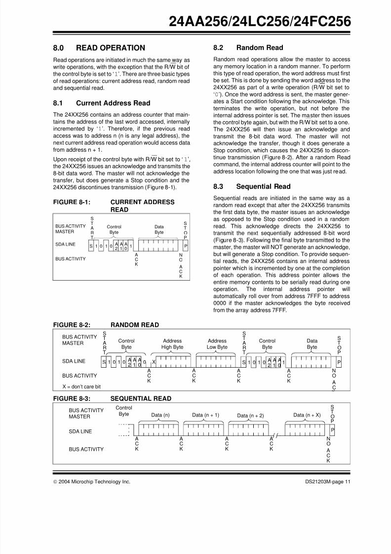
i2c EEPROM 24xx256 Ds
29
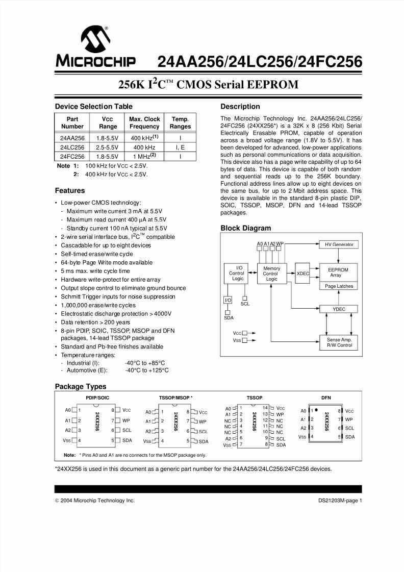
2004 Microchip Technology Inc. DS21203M-page 1 24AA256/24LC256/24FC256 Device Selecti on Tab le Features Low-power CMOS techno logy: - Max imum wr ite current 3 mA at 5. 5V - Maximum read current 400 µA at 5.5V - St and by cur rent 100 nA ty pic al at 5.5V • 2-wire serial int erf ace bu s, I 2 C ™ compatible • Cascadable for u p to eight devices • Sel f-t ime d erase/wr ite cyc le • 64-byte Page Write mode available • 5 ms max. wr it e cy cl e t ime • Hardware wr ite-pr otect for en tire array • Outp ut slope c ontro l to elimi nate gr ound bounce • Schmit t Tri gger inp uts for no ise supp ressio n • 1,000,000 erase/ wri te cycl es • Elect rosta tic di scharg e prote ction > 4000V • Data ret ent ion > 200 y ear s • 8-pin PDIP , SOIC, T SSOP , MSOP and DFN packages, 14-lead TSSOP package • St andar d and Pb-f ree finishes available • T empera ture ranges : Description The Microchip Technology Inc. 24AA256/24LC256/ 24FC256 (24XX256*) is a 32K x 8 (256 Kbit) Serial Electrically Erasable PROM, capable of operation across a broad voltage range (1.8V to 5.5V). It has been developed for advanced, low-power applications such as personal communications or data acquisition. This device also has a page write capability of up to 64 bytes of data. This device is capable of both random and sequential reads up to the 256K boundary. Functional address lines allow up to eight devices on the same bus, for up to 2 Mbit address space. Thi s device is available in the standard 8-pin plastic DIP, SOIC, TSSOP, MSOP, DFN and 14-lead TSSOP packages. Block Diagram Package Types *24XX256 is used in this document as a generic part number for the 24AA256/24LC256/24FC256 devices. Part Number VCC Range Max. Clock Frequency Temp. Ranges 24AA256 1.8-5.5V 400k Hz (1) I 24LC256 2.5-5.5V 400 kHz I, E 24FC256 1.8-5.5V 1 MHz (2) I Note 1: 100 kHz for VCC < 2.5V. 2: 400 kHz for VCC < 2.5V. - Industrial (I): -40°C to +85°C - Automotive (E): -40°C to +125°C HV Generator EEPROM Array Page Latches YDEC XDEC Sense Amp. R/W Control Memory Control Logic I/O Control Logic I/O A0 A1A2 SDA SCL VCC VSS WP A0 A1 A2 VSS VCC WP SCL SDA 1 2 3 4 8 7 6 5 2 4 X X 2 5 6 PDIP/SOIC TSSOP/MSOP * A0 A1 A2 VSS 1 2 3 4 8 7 6 5 VCC WP SCL SDA TSSOP 2 4 X X 2 5 6 DFN A0 A1 A2 VSS WP SCL SDA 2 4 X X 2 5 6 5 6 7 8 4 3 2 1 VCC NC A0 A1 NC A2 VSS NC NC VCC WP NC SCL SDA NC 2 4 X X 2 5 6 1 2 3 4 14 13 12 11 5 10 6 9 7 8 Note: * Pins A0 and A1 are no connects f or the MSOP package only. 256K I 2 C ™ CMOS Serial EEPROM
-
Upload
rizwan-amir -
Category
Documents
-
view
243 -
download
0
Transcript of i2c EEPROM 24xx256 Ds
8/8/2019 i2c EEPROM 24xx256 Ds
http://slidepdf.com/reader/full/i2c-eeprom-24xx256-ds 1/28
2004 Microchip Technology Inc. DS21203M-page 1
24AA256/24LC256/24FC256
Device Selection Table
Features
Low-power CMOS technology:
- Maximum write current 3 mA at 5.5V
- Maximum read current 400 µA at 5.5V
- Standby current 100 nA typical at 5.5V
• 2-wire serial interface bus, I2C™ compatible
• Cascadable for up to eight devices
• Self-timed erase/write cycle
• 64-byte Page Write mode available
• 5 ms max. write cycle time
• Hardware write-protect for entire array
• Output slope control to eliminate ground bounce
• Schmitt Trigger inputs for noise suppression
• 1,000,000 erase/write cycles
• Electrostatic discharge protection > 4000V
• Data retention > 200 years
• 8-pin PDIP, SOIC, TSSOP, MSOP and DFN
packages, 14-lead TSSOP package
• Standard and Pb-free finishes available
• Temperature ranges:
Description
The Microchip Technology Inc. 24AA256/24LC256/
24FC256 (24XX256*) is a 32K x 8 (256 Kbit) Serial
Electrically Erasable PROM, capable of operation
across a broad voltage range (1.8V to 5.5V). It has
been developed for advanced, low-power applications
such as personal communications or data acquisition.
This device also has a page write capability of up to 64
bytes of data. This device is capable of both random
and sequential reads up to the 256K boundary.
Functional address lines allow up to eight devices on
the same bus, for up to 2 Mbit address space. This
device is available in the standard 8-pin plastic DIP,SOIC, TSSOP, MSOP, DFN and 14-lead TSSOP
packages.
Block Diagram
Package Types
*24XX256 is used in this document as a generic part number for the 24AA256/24LC256/24FC256 devices.
Part
Number
VCC
Range
Max. Clock
Frequency
Temp.
Ranges
24AA256 1.8-5.5V 400 kHz(1) I
24LC256 2.5-5.5V 400 kHz I, E
24FC256 1.8-5.5V 1 MHz(2) I
Note 1: 100 kHz for VCC < 2.5V.
2: 400 kHz for VCC < 2.5V.
- Industrial (I): -40°C to +85°C
- Automotive (E): -40°C to +125°C
HV Generator
EEPROMArray
Page Latches
YDEC
XDEC
Sense Amp.R/W Control
MemoryControl
Logic
I/OControl
Logic
I/O
A0 A1A2
SDA
SCL
VCC
VSS
WP
A0
A1
A2
VSS
VCC
WP
SCL
SDA
1
2
3
4
8
7
6
5
2 4 X X 2 5 6
PDIP/SOIC TSSOP/MSOP *
A0
A1
A2
VSS
1
2
3
4
8
7
6
5
VCC
WP
SCL
SDA
TSSOP
2 4 X X 2 5 6
DFN
A0
A1
A2
VSS
WP
SCL
SDA
2 4 X X 2 5 6
5
6
7
8
4
3
2
1 VCC
NC
A0
A1
NC
A2
VSS
NC
NC
VCC
WP
NC
SCL
SDA
NC
2 4 X X 2 5 6
1
2
3
4
14
13
12
11
5 10
6 9
7 8
Note: * Pins A0 and A1 are no connects for the MSOP package only.
256K I2C™ CMOS Serial EEPROM
8/8/2019 i2c EEPROM 24xx256 Ds
http://slidepdf.com/reader/full/i2c-eeprom-24xx256-ds 2/28
24AA256/24LC256/24FC256
DS21203M-page 2 2004 Microchip Technology Inc.
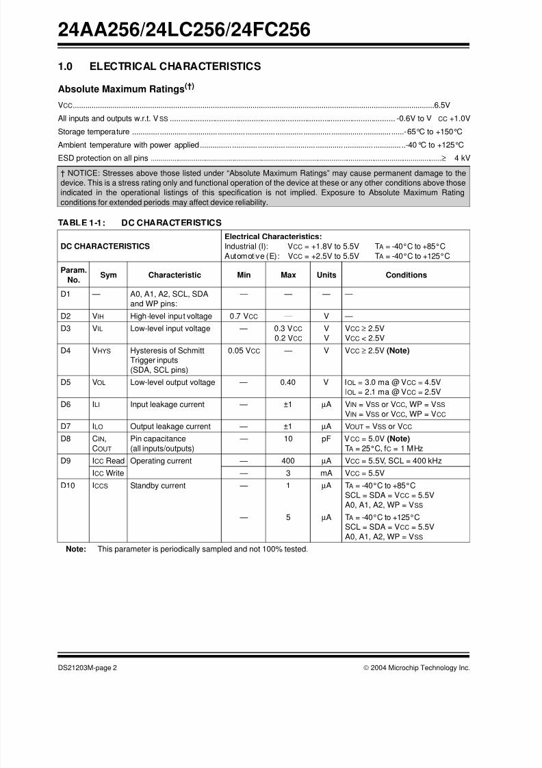
1.0 ELECTRICAL CHARACTERISTICS
Absolute Maximum Ratings(†)
VCC.............................................................................................................................................................................6.5V
All inputs and outputs w.r.t. VSS ......................................................................................................... -0.6V to VCC +1.0V
Storage temperature ...............................................................................................................................-65°C to +150°CAmbient temperature with power applied................................................................................................-40°C to +125°C
ESD protection on all pins ......................................................................................................................................................≥ 4 kV
TABLE 1-1: DC CHARACTERISTICS
† NOTICE: Stresses above those listed under “Absolute Maximum Ratings” may cause permanent damage to the
device. This is a stress rating only and functional operation of the device at these or any other conditions above those
indicated in the operational listings of this specification is not implied. Exposure to Absolute Maximum Rating
conditions for extended periods may affect device reliability.
DC CHARACTERISTICS
Electrical Characteristics:
Industrial (I): VCC = +1.8V to 5.5V TA = -40°C to +85°C
Automotive (E): VCC = +2.5V to 5.5V TA = -40°C to +125°C
Param.No.
Sym Characteristic Min Max Units Conditions
D1 — A0, A1, A2, SCL, SDA
and WP pins:
— — — —
D2 VIH High-level input voltage 0.7 VCC — V —
D3 VIL Low-level input voltage — 0.3 VCC
0.2 VCC
V
V
VCC ≥ 2.5V
VCC < 2.5V
D4 VHYS Hysteresis of Schmitt
Trigger inputs
(SDA, SCL pins)
0.05 VCC — V VCC ≥ 2.5V (Note)
D5 VOL Low-level output voltage — 0.40 V IOL = 3.0 ma @ VCC = 4.5V
IOL = 2.1 ma @ VCC = 2.5V
D6 ILI Input leakage current — ±1 µA VIN = VSS or VCC, WP = VSS
VIN = VSS or VCC, WP = VCC
D7 ILO Output leakage current — ±1 µA VOUT = VSS or VCC
D8 CIN,
COUT
Pin capacitance
(all inputs/outputs)
— 10 pF VCC = 5.0V (Note)
TA = 25°C, fC = 1 MHz
D9 ICC Read Operating current — 400 µA VCC = 5.5V, SCL = 400 kHz
ICC Write — 3 mA VCC = 5.5V
D10 ICCS Standby current — 1 µA TA = -40°C to +85°C
SCL = SDA = VCC = 5.5V
A0, A1, A2, WP = VSS
— 5 µA TA = -40°C to +125°C
SCL = SDA = VCC = 5.5V
A0, A1, A2, WP = VSS
Note: This parameter is periodically sampled and not 100% tested.
8/8/2019 i2c EEPROM 24xx256 Ds
http://slidepdf.com/reader/full/i2c-eeprom-24xx256-ds 3/28
2004 Microchip Technology Inc. DS21203M-page 3
24AA256/24LC256/24FC256
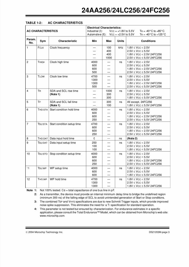
TABLE 1-2: AC CHARACTERISTICS
AC CHARACTERISTICS
Electrical Characteristics:
Industrial (I): VCC = +1.8V to 5.5V TA = -40°C to +85°C
Automotive (E): VCC = +2.5V to 5.5V TA = -40°C to +125°C
Param.
No.Sym Characteristic Min Max Units Conditions
1 FCLK Clock frequency — —
—
—
100400
400
1000
kHz 1.8V ≤ VCC < 2.5V2.5V ≤ VCC ≤ 5.5V
1.8V ≤ VCC < 2.5V 24FC256
2.5V ≤ VCC ≤ 5.5V 24FC256
2 THIGH Clock high time 4000
600
600
500
—
—
—
—
ns 1.8V ≤ VCC < 2.5V
2.5V ≤ VCC ≤ 5.5V
1.8V ≤ VCC < 2.5V 24FC256
2.5V ≤ VCC ≤ 5.5V 24FC256
3 TLOW Clock low time 4700
1300
1300
500
—
—
—
—
ns 1.8V ≤ VCC < 2.5V
2.5V ≤ VCC ≤ 5.5V
1.8V ≤ VCC < 2.5V 24FC256
2.5V ≤ VCC ≤ 5.5V 24FC256
4 TR SDA and SCL rise time
(Note 1)
—
— —
1000
300300
ns 1.8V ≤ VCC < 2.5V
2.5V ≤ VCC ≤ 5.5V1.8V ≤ VCC ≤ 5.5V 24FC256
5 TF SDA and SCL fall time
(Note 1)
—
—
300
100
ns All except, 24FC256
1.8V ≤ VCC ≤ 5.5V 24FC256
6 THD:STA Start condition hold time 4000
600
600
250
—
—
—
—
ns 1.8V ≤ VCC < 2.5V
2.5V ≤ VCC ≤ 5.5V
1.8V ≤ VCC < 2.5V 24FC256
2.5V ≤ VCC ≤ 5.5V 24FC256
7 TSU:STA Start condition setup time 4700
600
600
250
—
—
—
—
ns 1.8V ≤ VCC < 2.5V
2.5V ≤ VCC ≤ 5.5V
1.8V ≤ VCC < 2.5V 24FC256
2.5V ≤ VCC ≤ 5.5V 24FC256
8 THD:DAT Data input hold time 0 — ns (Note 2)
9 TSU:DAT Data input setup time 250
100
100
—
—
—
ns 1.8V ≤ VCC < 2.5V
2.5V ≤ VCC ≤ 5.5V
1.8V ≤ VCC ≤ 5.5V 24FC256
10 TSU:STO Stop condition setup time 4000
600
600
250
—
—
—
—
ns 1.8V ≤ VCC < 2.5V
2.5V ≤ VCC ≤ 5.5V
1.8V ≤ VCC < 2.5V 24FC256
2.5V ≤ VCC ≤ 5.5V 24FC256
11 TSU:WP WP setup time 4000
600
600
—
—
—
ns 1.8V ≤ VCC < 2.5V
2.5V ≤ VCC ≤ 5.5V
1.8V ≤ VCC ≤ 5.5V 24FC256
12 THD:WP WP hold time 4700
1300
1300
—
—
—
ns 1.8V ≤ VCC < 2.5V
2.5V ≤ VCC ≤ 5.5V
1.8V ≤ VCC ≤ 5.5V 24FC256Note 1: Not 100% tested. CB = total capacitance of one bus line in pF.
2: As a transmitter, the device must provide an internal minimum delay time to bridge the undefined region
(minimum 300 ns) of the falling edge of SCL to avoid unintended generation of Start or Stop conditions.
3: The combined TSP and VHYS specifications are due to new Schmitt Trigger inputs, which provide improved
noise spike suppression. This eliminates the need for a TI specification for standard operation.
4: This parameter is not tested but ensured by characterization. For endurance estimates in a specific
application, please consult the Total Endurance™ Model, which can be obtained from Microchip’s web site:
www.microchip.com.
8/8/2019 i2c EEPROM 24xx256 Ds
http://slidepdf.com/reader/full/i2c-eeprom-24xx256-ds 4/28
24AA256/24LC256/24FC256
DS21203M-page 4 2004 Microchip Technology Inc.
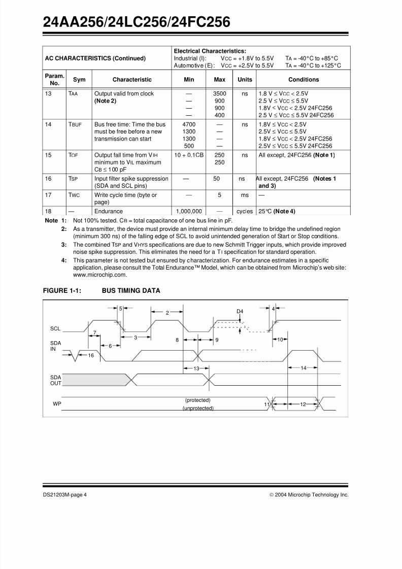
FIGURE 1-1: BUS TIMING DATA
13 TAA Output valid from clock
(Note 2)
—
— —
—
3500
900900
400
ns 1.8 V ≤ VCC < 2.5V
2.5 V ≤ VCC ≤ 5.5V1.8V ≤ VCC < 2.5V 24FC256
2.5 V ≤ VCC ≤ 5.5V 24FC256
14 TBUF Bus free time: Time the bus
must be free before a new
transmission can start
4700
1300
1300
500
—
—
—
—
ns 1.8V ≤ VCC < 2.5V
2.5V ≤ VCC ≤ 5.5V
1.8V ≤ VCC < 2.5V 24FC256
2.5V ≤ VCC ≤ 5.5V 24FC256
15 TOF Output fall time from VIH
minimum to VIL maximum
CB ≤ 100 pF
10 + 0.1CB 250
250
ns All except, 24FC256 (Note 1)
16 TSP Input filter spike suppression
(SDA and SCL pins)
— 50 ns All except, 24FC256 (Notes 1
and 3)
17 TWC Write cycle time (byte or
page)
— 5 ms —
18 — Endurance 1,000,000 — cycles 25°C (Note 4)
AC CHARACTERISTICS (Continued)
Electrical Characteristics:
Industrial (I): VCC = +1.8V to 5.5V TA = -40°C to +85°C
Automotive (E): VCC = +2.5V to 5.5V TA = -40°C to +125°C
Param.
No.Sym Characteristic Min Max Units Conditions
Note 1: Not 100% tested. CB = total capacitance of one bus line in pF.
2: As a transmitter, the device must provide an internal minimum delay time to bridge the undefined region
(minimum 300 ns) of the falling edge of SCL to avoid unintended generation of Start or Stop conditions.
3: The combined TSP and VHYS specifications are due to new Schmitt Trigger inputs, which provide improved
noise spike suppression. This eliminates the need for a TI specification for standard operation.
4: This parameter is not tested but ensured by characterization. For endurance estimates in a specific
application, please consult the Total Endurance™ Model, which can be obtained from Microchip’s web site:
www.microchip.com.
(unprotected)
(protected)
SCL
SDAIN
SDAOUT
WP
5
7
6
16
3
2
8 9
13
D4 4
10
11 12
14
8/8/2019 i2c EEPROM 24xx256 Ds
http://slidepdf.com/reader/full/i2c-eeprom-24xx256-ds 5/28
2004 Microchip Technology Inc. DS21203M-page 5
24AA256/24LC256/24FC256
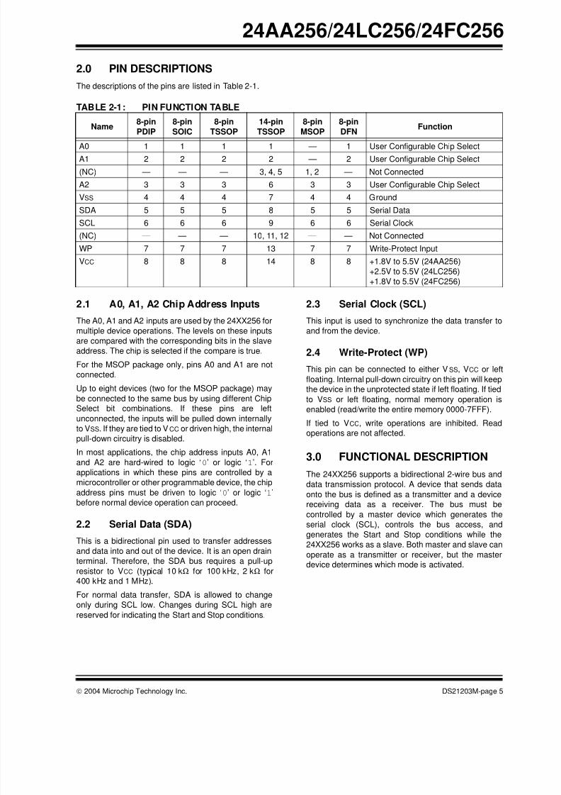
2.0 PIN DESCRIPTIONS
The descriptions of the pins are listed in Table 2-1.
TABLE 2-1: PIN FUNCTION TABLE
2.1 A0, A1, A2 Chip Address Inputs
The A0, A1 and A2 inputs are used by the 24XX256 for
multiple device operations. The levels on these inputs
are compared with the corresponding bits in the slave
address. The chip is selected if the compare is true.
For the MSOP package only, pins A0 and A1 are not
connected.
Up to eight devices (two for the MSOP package) may
be connected to the same bus by using different Chip
Select bit combinations. If these pins are left
unconnected, the inputs will be pulled down internallyto VSS. If they are tied to VCC or driven high, the internal
pull-down circuitry is disabled.
In most applications, the chip address inputs A0, A1
and A2 are hard-wired to logic ‘0’ or logic ‘1’. For
applications in which these pins are controlled by a
microcontroller or other programmable device, the chip
address pins must be driven to logic ‘0’ or logic ‘1’
before normal device operation can proceed.
2.2 Serial Data (SDA)
This is a bidirectional pin used to transfer addresses
and data into and out of the device. It is an open drain
terminal. Therefore, the SDA bus requires a pull-up
resistor to VCC (typical 10 kΩ for 100 kHz, 2 kΩ for
400 kHz and 1 MHz).
For normal data transfer, SDA is allowed to change
only during SCL low. Changes during SCL high are
reserved for indicating the Start and Stop conditions.
2.3 Serial Clock (SCL)
This input is used to synchronize the data transfer to
and from the device.
2.4 Write-Protect (WP)
This pin can be connected to either VSS, VCC or left
floating. Internal pull-down circuitry on this pin will keep
the device in the unprotected state if left floating. If tied
to VSS or left floating, normal memory operation is
enabled (read/write the entire memory 0000-7FFF).
If tied to VCC, write operations are inhibited. Read
operations are not affected.
3.0 FUNCTIONAL DESCRIPTION
The 24XX256 supports a bidirectional 2-wire bus and
data transmission protocol. A device that sends data
onto the bus is defined as a transmitter and a device
receiving data as a receiver. The bus must be
controlled by a master device which generates the
serial clock (SCL), controls the bus access, and
generates the Start and Stop conditions while the
24XX256 works as a slave. Both master and slave can
operate as a transmitter or receiver, but the masterdevice determines which mode is activated.
Name8-pin
PDIP
8-pin
SOIC
8-pin
TSSOP
14-pin
TSSOP
8-pin
MSOP
8-pin
DFNFunction
A0 1 1 1 1 — 1 User Configurable Chip Select
A1 2 2 2 2 — 2 User Configurable Chip Select
(NC) — — — 3, 4, 5 1, 2 — Not Connected
A2 3 3 3 6 3 3 User Configurable Chip Select
VSS 4 4 4 7 4 4 Ground
SDA 5 5 5 8 5 5 Serial Data
SCL 6 6 6 9 6 6 Serial Clock
(NC) — — — 10, 11, 12 — — Not Connected
WP 7 7 7 13 7 7 Write-Protect Input
VCC 8 8 8 14 8 8 +1.8V to 5.5V (24AA256)
+2.5V to 5.5V (24LC256)
+1.8V to 5.5V (24FC256)
8/8/2019 i2c EEPROM 24xx256 Ds
http://slidepdf.com/reader/full/i2c-eeprom-24xx256-ds 6/28
24AA256/24LC256/24FC256
DS21203M-page 6 2004 Microchip Technology Inc.
4.0 BUS CHARACTERISTICS
The following bus protocol has been defined:
• Data transfer may be initiated only when the bus
is not busy.
• During data transfer, the data line must remain
stable whenever the clock line is high. Changes
in the data line, while the clock line is high, will beinterpreted as a Start or Stop condition.
Accordingly, the following bus conditions have been
defined (Figure 4-1).
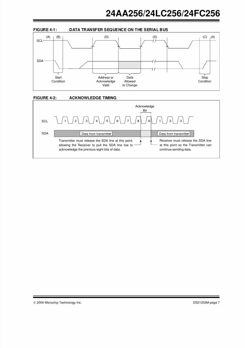
4.1 Bus not Busy (A)
Both data and clock lines remain high.
4.2 Start Data Transfer (B)
A high-to-low transition of the SDA line while the clock
(SCL) is high, determines a Start condition. All
commands must be preceded by a Start condition.
4.3 Stop Data Transfer (C)
A low-to-high transition of the SDA line, while the clock
(SCL) is high, determines a Stop condition. All
operations must end with a Stop condition.
4.4 Data Valid (D)
The state of the data line represents valid data when,
after a Start condition, the data line is stable for the
duration of the high period of the clock signal.
The data on the line must be changed during the low
period of the clock signal. There is one bit of data per
clock pulse.
Each data transfer is initiated with a Start condition and
terminated with a Stop condition. The number of the
data bytes transferred between the Start and Stop
conditions is determined by the master device.
4.5 Acknowledge
Each receiving device, when addressed, is obliged to
generate an Acknowledge signal after the reception of
each byte. The master device must generate an extra
clock pulse which is associated with this Acknowledge
bit.
A device that acknowledges must pull down the SDA
line during the acknowledge clock pulse in such a way
that the SDA line is stable low during the high period of
the acknowledge related clock pulse. Of course, setup
and hold times must be taken into account. During
reads, a master must signal an end of data to the slave
by NOT generating an Acknowledge bit on the last byte
that has been clocked out of the slave. In this case, the
slave (24XX256) will leave the data line high to enable
the master to generate the Stop condition.
Note: The 24XX256 does not generate anyAcknowledge bits if an internal
programming cycle is in progress.
8/8/2019 i2c EEPROM 24xx256 Ds
http://slidepdf.com/reader/full/i2c-eeprom-24xx256-ds 7/28
2004 Microchip Technology Inc. DS21203M-page 7
24AA256/24LC256/24FC256
FIGURE 4-1: DATA TRANSFER SEQUENCE ON THE SERIAL BUS
FIGURE 4-2: ACKNOWLEDGE TIMING
Address orAcknowledge
Valid
DataAllowed
to Change
StopCondition
StartCondition
SCL
SDA
(A) (B) (D) (D) (C) (A)
SCL 987654321 1 2 3
Transmitter must release the SDA line at this point,
allowing the Receiver to pull the SDA line low to
acknowledge the previous eight bits of data.
Receiver must release the SDA line
at this point so the Transmitter can
continue sending data.
Data from transmitterSDA
Acknowledge
Bit
Data from transmitter
8/8/2019 i2c EEPROM 24xx256 Ds
http://slidepdf.com/reader/full/i2c-eeprom-24xx256-ds 8/28
24AA256/24LC256/24FC256
DS21203M-page 8 2004 Microchip Technology Inc.
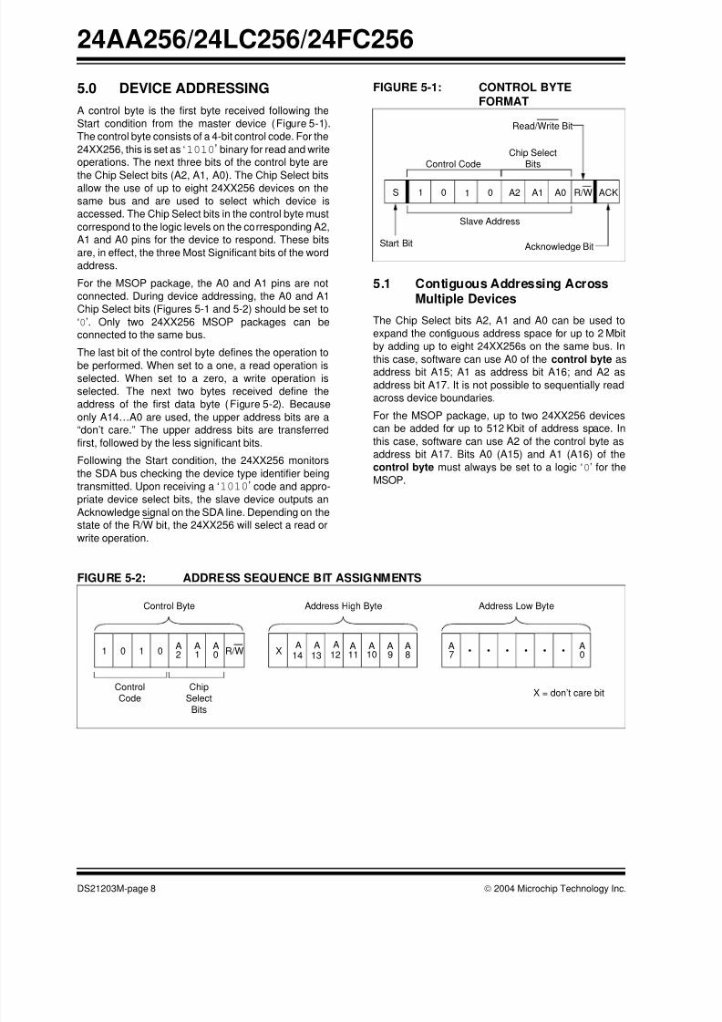
5.0 DEVICE ADDRESSING
A control byte is the first byte received following the
Start condition from the master device (Figure 5-1).
The control byte consists of a 4-bit control code. For the
24XX256, this is set as ‘1010’ binary for read and write
operations. The next three bits of the control byte are
the Chip Select bits (A2, A1, A0). The Chip Select bitsallow the use of up to eight 24XX256 devices on the
same bus and are used to select which device is
accessed. The Chip Select bits in the control byte must
correspond to the logic levels on the corresponding A2,
A1 and A0 pins for the device to respond. These bits
are, in effect, the three Most Significant bits of the word
address.
For the MSOP package, the A0 and A1 pins are not
connected. During device addressing, the A0 and A1
Chip Select bits (Figures 5-1 and 5-2) should be set to
‘0’. Only two 24XX256 MSOP packages can be
connected to the same bus.
The last bit of the control byte defines the operation tobe performed. When set to a one, a read operation is
selected. When set to a zero, a write operation is
selected. The next two bytes received define the
address of the first data byte (Figure 5-2). Because
only A14…A0 are used, the upper address bits are a
“don’t care.” The upper address bits are transferred
first, followed by the less significant bits.
Following the Start condition, the 24XX256 monitors
the SDA bus checking the device type identifier being
transmitted. Upon receiving a ‘1010’ code and appro-
priate device select bits, the slave device outputs an
Acknowledge signal on the SDA line. Depending on the
state of the R/W bit, the 24XX256 will select a read or
write operation.
FIGURE 5-1: CONTROL BYTE
FORMAT
5.1 Contiguous Addressing AcrossMultiple Devices
The Chip Select bits A2, A1 and A0 can be used to
expand the contiguous address space for up to 2 Mbit
by adding up to eight 24XX256s on the same bus. In
this case, software can use A0 of the control byte asaddress bit A15; A1 as address bit A16; and A2 as
address bit A17. It is not possible to sequentially read
across device boundaries.
For the MSOP package, up to two 24XX256 devices
can be added for up to 512 Kbit of address space. In
this case, software can use A2 of the control byte as
address bit A17. Bits A0 (A15) and A1 (A16) of the
control byte must always be set to a logic ‘0’ for the
MSOP.
FIGURE 5-2: ADDRESS SEQUENCE BIT ASSIGNMENTS
1 0 1 0 A2 A1 A0S ACKR/W
Control CodeChip Select
Bits
Slave Address
Acknowledge BitStart Bit
Read/Write Bit
1 0 1 0A2
A1
A0 R/W X
A11
A10
A9
A7
A0
A8 • • • • • •
A12
Control Byte Address High Byte Address Low Byte
ControlCode
ChipSelect
Bits
X = don’t care bit
A13
A14
8/8/2019 i2c EEPROM 24xx256 Ds
http://slidepdf.com/reader/full/i2c-eeprom-24xx256-ds 9/28
2004 Microchip Technology Inc. DS21203M-page 9
24AA256/24LC256/24FC256
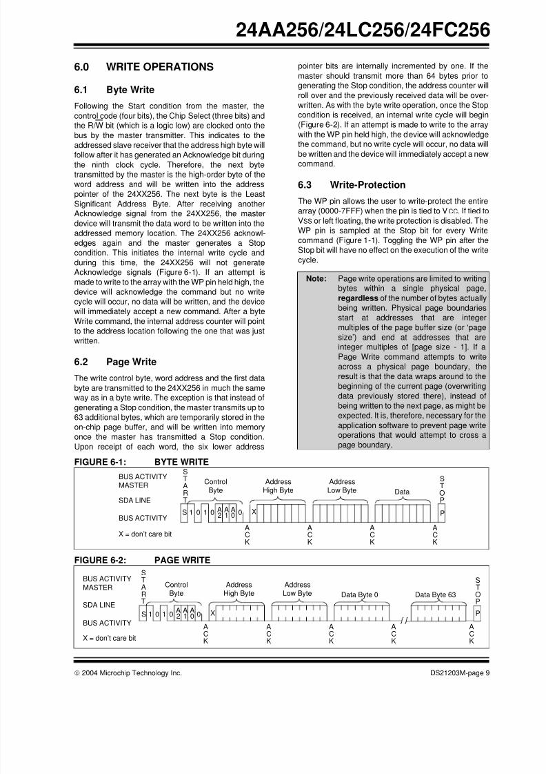
6.0 WRITE OPERATIONS
6.1 Byte Write
Following the Start condition from the master, the
control code (four bits), the Chip Select (three bits) and
the R/W bit (which is a logic low) are clocked onto the
bus by the master transmitter. This indicates to theaddressed slave receiver that the address high byte will
follow after it has generated an Acknowledge bit during
the ninth clock cycle. Therefore, the next byte
transmitted by the master is the high-order byte of the
word address and will be written into the address
pointer of the 24XX256. The next byte is the Least
Significant Address Byte. After receiving another
Acknowledge signal from the 24XX256, the master
device will transmit the data word to be written into the
addressed memory location. The 24XX256 acknowl-
edges again and the master generates a Stop
condition. This initiates the internal write cycle and
during this time, the 24XX256 will not generate
Acknowledge signals (Figure 6-1). If an attempt ismade to write to the array with the WP pin held high, the
device will acknowledge the command but no write
cycle will occur, no data will be written, and the device
will immediately accept a new command. After a byte
Write command, the internal address counter will point
to the address location following the one that was just
written.
6.2 Page Write
The write control byte, word address and the first data
byte are transmitted to the 24XX256 in much the same
way as in a byte write. The exception is that instead of
generating a Stop condition, the master transmits up to63 additional bytes, which are temporarily stored in the
on-chip page buffer, and will be written into memory
once the master has transmitted a Stop condition.
Upon receipt of each word, the six lower address
pointer bits are internally incremented by one. If the
master should transmit more than 64 bytes prior to
generating the Stop condition, the address counter will
roll over and the previously received data will be over-
written. As with the byte write operation, once the Stop
condition is received, an internal write cycle will begin
(Figure 6-2). If an attempt is made to write to the array
with the WP pin held high, the device will acknowledgethe command, but no write cycle will occur, no data will
be written and the device will immediately accept a new
command.
6.3 Write-Protection
The WP pin allows the user to write-protect the entire
array (0000-7FFF) when the pin is tied to VCC. If tied to
VSS or left floating, the write protection is disabled. The
WP pin is sampled at the Stop bit for every Write
command (Figure 1-1). Toggling the WP pin after the
Stop bit will have no effect on the execution of the write
cycle.
FIGURE 6-1: BYTE WRITE
FIGURE 6-2: PAGE WRITE
Note: Page write operations are limited to writing
bytes within a single physical page,
regardless of the number of bytes actually
being written. Physical page boundaries
start at addresses that are integer
multiples of the page buffer size (or ‘page
size’) and end at addresses that are
integer multiples of [page size - 1]. If a
Page Write command attempts to write
across a physical page boundary, the
result is that the data wraps around to the
beginning of the current page (overwriting
data previously stored there), instead of
being written to the next page, as might beexpected. It is, therefore, necessary for the
application software to prevent page write
operations that would attempt to cross a
page boundary.
X
BUS ACTIVITYMASTER
SDA LINE
BUS ACTIVITY
START
ControlByte
AddressHigh Byte
AddressLow Byte Data
STOP
AC
K
AC
K
AC
K
AC
K
X = don’t care bit
S 1 0 1 0 0A2
A1
A0 P
X
BUS ACTIVITY
MASTER
SDA LINE
BUS ACTIVITY
START
ControlByte
AddressHigh Byte
AddressLow Byte Data Byte 0
STOP
ACK
ACK
ACK
ACK
Data Byte 63
ACKX = don’t care bit
S 1 0 1 0 0A2
A1
A0 P
8/8/2019 i2c EEPROM 24xx256 Ds
http://slidepdf.com/reader/full/i2c-eeprom-24xx256-ds 10/28
24AA256/24LC256/24FC256
DS21203M-page 10 2004 Microchip Technology Inc.
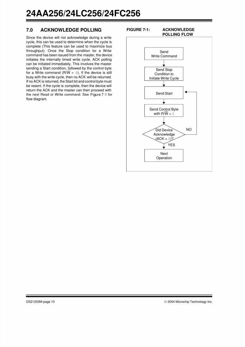
7.0 ACKNOWLEDGE POLLING
Since the device will not acknowledge during a write
cycle, this can be used to determine when the cycle is
complete (This feature can be used to maximize bus
throughput). Once the Stop condition for a Write
command has been issued from the master, the device
initiates the internally timed write cycle. ACK pollingcan be initiated immediately. This involves the master
sending a Start condition, followed by the control byte
for a Write command (R/W = 0). If the device is still
busy with the write cycle, then no ACK will be returned.
If no ACK is returned, the Start bit and control byte must
be resent. If the cycle is complete, then the device will
return the ACK and the master can then proceed with
the next Read or Write command. See Figure 7-1 for
flow diagram.
FIGURE 7-1: ACKNOWLEDGE
POLLING FLOW
SendWrite Command
Send Stop
Condition to
Initiate Write Cycle
Send Start
Send Control Byte
with R/W = 0
Did DeviceAcknowledge
(ACK = 0)?
Next
Operation
NO
YES
8/8/2019 i2c EEPROM 24xx256 Ds
http://slidepdf.com/reader/full/i2c-eeprom-24xx256-ds 11/28
8/8/2019 i2c EEPROM 24xx256 Ds
http://slidepdf.com/reader/full/i2c-eeprom-24xx256-ds 12/28
24AA256/24LC256/24FC256
DS21203M-page 12 2004 Microchip Technology Inc.
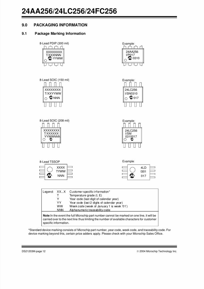
9.0 PACKAGING INFORMATION
9.1 Package Marking Information
XXXXXXXXT/XXXNNN
YYWW
8-Lead PDIP (300 mil) Example:
8-Lead TSSOP Example:
8-Lead SOIC (150 mil) Example:
XXXXXXXX
T/XXYYWW
NNN
XXXX
TYWW
NNN
8-Lead SOIC (208 mil) Example:
24LC256
0310017I/SM
24AA256I/P017
0310
XXXXXXXX
YYWWNNNT/XXXXXX
24LC256
I/SN0310
017
4LD
I301
017
Legend: XX...X Customer specific information*
T Temperature grade (I, E)
Y Year code (last digit of calendar year)
YY Year code (last 2 digits of calendar year)WW Week code (week of January 1 is week ‘01’)
NNN Alphanumeric traceability code
Note:In the event the full Microchip part number cannot be marked on one line, it will be
carried over to the next line thus limiting the number of available characters for customer
specific information.
*Standard device marking consists of Microchip part number, year code, week code, and traceability code. For
device marking beyond this, certain price adders apply. Please check with your Microchip Sales Office.
8/8/2019 i2c EEPROM 24xx256 Ds
http://slidepdf.com/reader/full/i2c-eeprom-24xx256-ds 13/28
2004 Microchip Technology Inc. DS21203M-page 13
24AA256/24LC256/24FC256
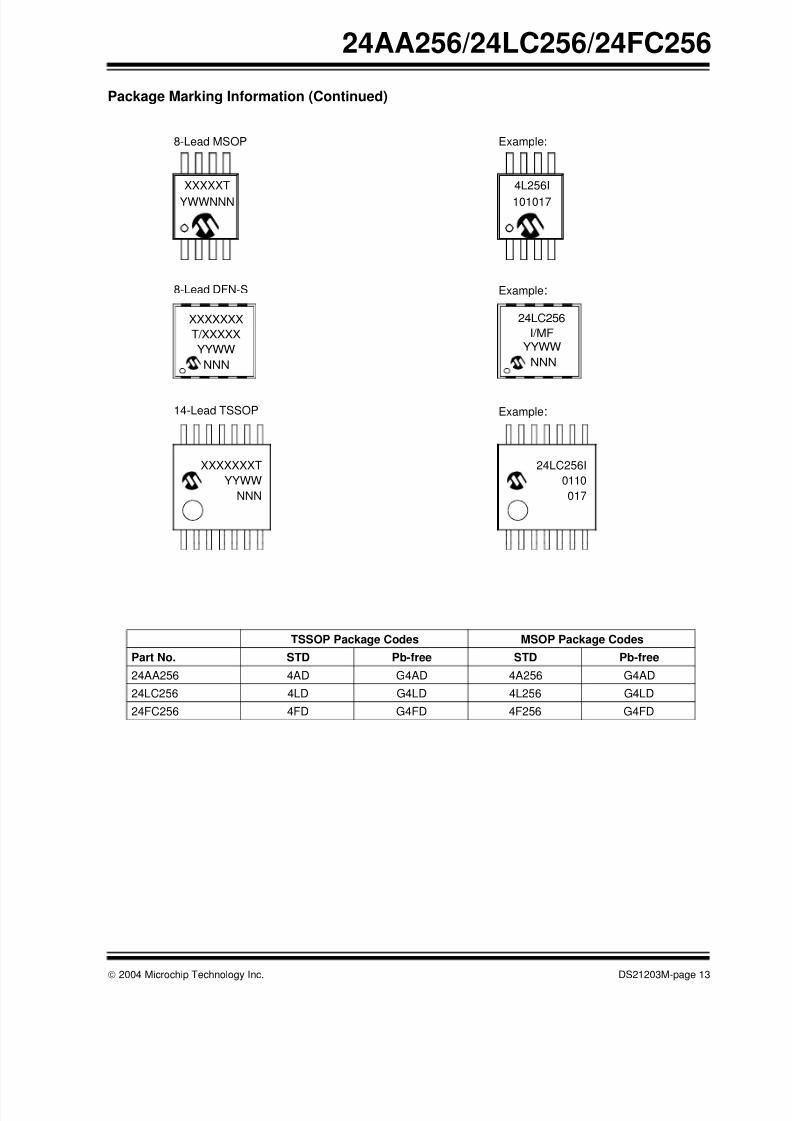
Package Marking Information (Continued)
14-Lead TSSOP Example:
XXXXXXXT
YYWW
NNN
8-Lead MSOP Example:
XXXXXT
YWWNNN
4L256I
101017
24LC256I
0110
017
8-Lead DFN-S Example:
XXXXXXX
T/XXXXX
YYWW
24LC256
I/MFYYWW
NNNNNN
TSSOP Package Codes MSOP Package Codes
Part No. STD Pb-free STD Pb-free
24AA256 4AD G4AD 4A256 G4AD
24LC256 4LD G4LD 4L256 G4LD
24FC256 4FD G4FD 4F256 G4FD
8/8/2019 i2c EEPROM 24xx256 Ds
http://slidepdf.com/reader/full/i2c-eeprom-24xx256-ds 14/28
24AA256/24LC256/24FC256
DS21203M-page 14 2004 Microchip Technology Inc.
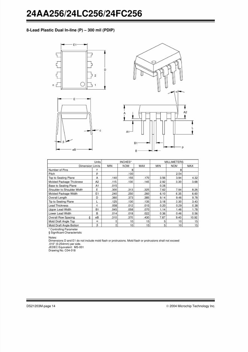
8-Lead Plastic Dual In-line (P) – 300 mil (PDIP)
B1
B
A1
A
L
A2
p
α
E
eB
β
c
E1
n
D
1
2
Units INCHES* MILLIMETERS
Dimension Limits MIN NOM MAX MIN NOM MAX
Number of Pins n 8 8
Pitch p .100 2.54
Top to Seating Plane A .140 .155 .170 3.56 3.94 4.32
Molded Package Thickness A2 .115 .130 .145 2.92 3.30 3.68
Base to Seating Plane A1 .015 0.38
Shoulder to Shoulder Width E .300 .313 .325 7.62 7.94 8.26
Molded Package Width E1 .240 .250 .260 6.10 6.35 6.60
Overall Length D .360 .373 .385 9.14 9.46 9.78
Tip to Seating Plane L .125 .130 .135 3.18 3.30 3.43
Lead Thickness c .008 .012 .015 0.20 0.29 0.38
Upper Lead Width B1 .045 .058 .070 1.14 1.46 1.78
Lower Lead Width B .014 .018 .022 0.36 0.46 0.56
Overall Row Spacing § eB .310 .370 .430 7.87 9.40 10.92
Mold Draft Angle Top α 5 10 15 5 10 15
Mold Draft Angle Bottom β 5 10 15 5 10 15
* Controlling Parameter
Notes:Dimensions D and E1 do not include mold flash or protrusions. Mold flash or protrusions shall not exceed
JEDEC Equivalent: MS-001Drawing No. C04-018
.010” (0.254mm) per side.
§ Significant Characteristic
8/8/2019 i2c EEPROM 24xx256 Ds
http://slidepdf.com/reader/full/i2c-eeprom-24xx256-ds 15/28
2004 Microchip Technology Inc. DS21203M-page 15
24AA256/24LC256/24FC256
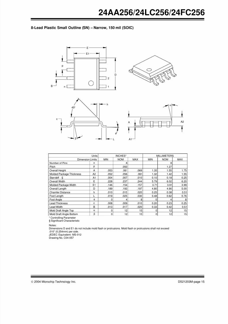
8-Lead Plastic Small Outline (SN) – Narrow, 150 mil (SOIC)
Foot Angle φ 0 4 8 0 4 8
1512015120βMold Draft Angle Bottom
1512015120αMold Draft Angle Top
0.510.420.33.020.017.013BLead Width
0.250.230.20.010.009.008cLead Thickness
0.760.620.48.030.025.019LFoot Length
0.510.380.25.020.015.010hChamfer Distance
5.004.904.80.197.193.189DOverall Length
3.993.913.71.157.154.146E1Molded Package Width
6.206.025.79.244.237.228EOverall Width
0.250.180.10.010.007.004A1Standoff §
1.551.421.32.061.056.052A2Molded Package Thickness1.751.551.35.069.061.053AOverall Height
1.27.050pPitch
88nNumber of Pins
MAXNOMMINMAXNOMMINDimension Limits
MILLIMETERSINCHES*Units
2
1
D
n
p
B
E
E1
h
Lβ
c
45°
φ
A2
α
A
A1
* Controlling Parameter
Notes:Dimensions D and E1 do not include mold flash or protrusions. Mold flash or protrusions shall not exceed.010” (0.254mm) per side.JEDEC Equivalent: MS-012Drawing No. C04-057
§ Significant Characteristic
8/8/2019 i2c EEPROM 24xx256 Ds
http://slidepdf.com/reader/full/i2c-eeprom-24xx256-ds 16/28
24AA256/24LC256/24FC256
DS21203M-page 16 2004 Microchip Technology Inc.
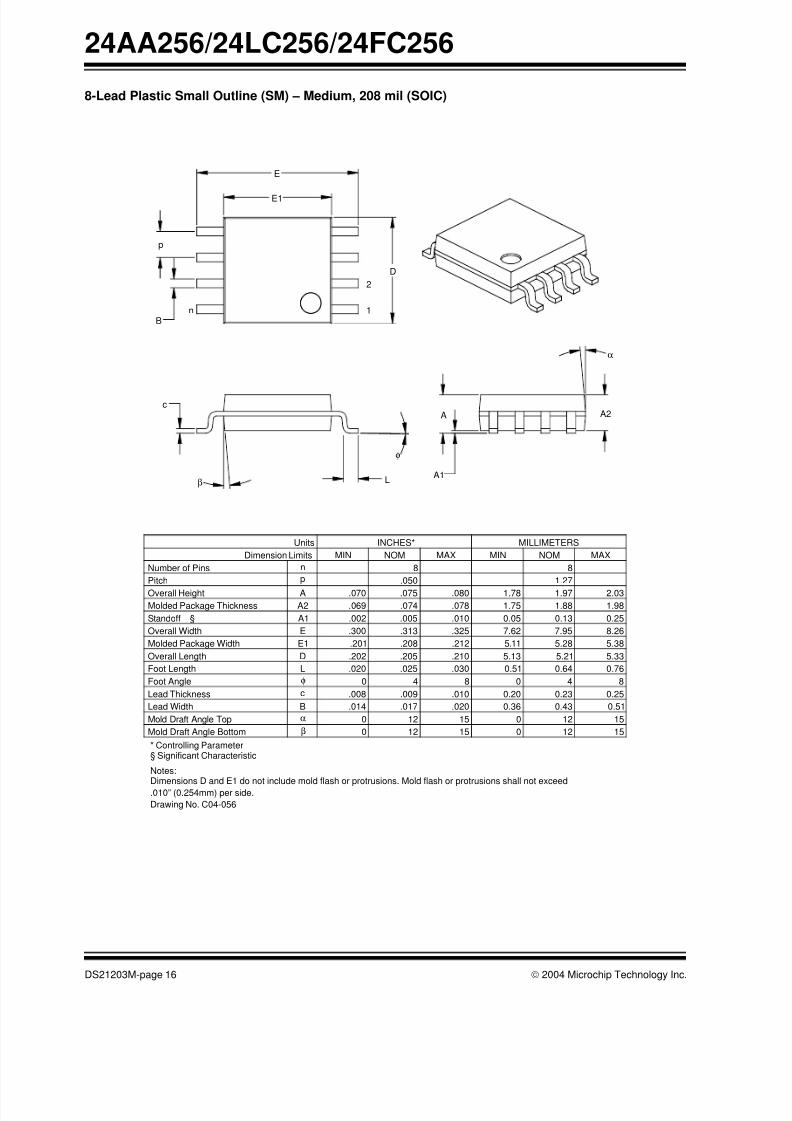
8-Lead Plastic Small Outline (SM) – Medium, 208 mil (SOIC)
Foot Angle φ 0 4 8 0 4 8
1512015120βMold Draft Angle Bottom
1512015120αMold Draft Angle Top
0.510.430.36.020.017.014BLead Width
0.250.230.20.010.009.008cLead Thickness
0.760.640.51.030.025.020LFoot Length
5.335.215.13.210.205.202DOverall Length
5.385.285.11.212.208.201E1Molded Package Width
8.267.957.62.325.313.300EOverall Width
0.250.130.05.010.005.002A1Standoff §
1.98.078A2Molded Package Thickness
2.03.080AOverall Height
1.27.050pPitch
88nNumber of Pins
MAXNOMMINMAXNOMMINDimension Limits
MILLIMETERSINCHES*Units
α
A2A
A1L
c
β
φ
2
1
D
n
p
B
E
E1
.070 .075
.069 .074
1.78
1.75
1.97
1.88
* Controlling Parameter
Notes:
Dimensions D and E1 do not include mold flash or protrusions. Mold flash or protrusions shall not exceed.010” (0.254mm) per side.
Drawing No. C04-056
§ Significant Characteristic
8/8/2019 i2c EEPROM 24xx256 Ds
http://slidepdf.com/reader/full/i2c-eeprom-24xx256-ds 17/28
2004 Microchip Technology Inc. DS21203M-page 17
24AA256/24LC256/24FC256
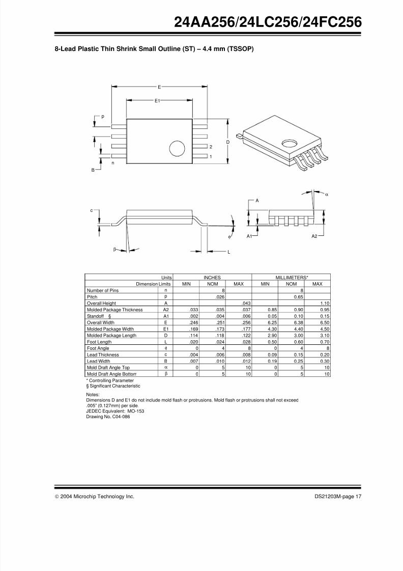
8-Lead Plastic Thin Shrink Small Outline (ST) – 4.4 mm (TSSOP)
10501050βMold Draft Angle Bottom
10501050αMold Draft Angle Top
0.300.250.19.012.010.007BLead Width
0.200.150.09.008.006.004cLead Thickness
0.700.600.50.028.024.020LFoot Length
3.103.002.90.122.118.114DMolded Package Length
4.504.404.30.177.173.169E1Molded Package Width
6.506.386.25.256.251.246EOverall Width
0.150.100.05.006.004.002A1Standoff §
0.950.900.85.037.035.033A2Molded Package Thickness
1.10.043AOverall Height
0.65.026pPitch
88nNumber of Pins
MAXNOMMINMAXNOMMINDimension Limits
MILLIMETERS*INCHESUnits
α
A2
A
A1
L
c
β
φ
1
2D
n
p
B
E
E1
Foot Angle φ 0 4 8 0 4 8
* Controlling Parameter
Notes:
Dimensions D and E1 do not include mold flash or protrusions. Mold flash or protrusions shall not exceed.005” (0.127mm) per side.JEDEC Equivalent: MO-153Drawing No. C04-086
§ Significant Characteristic
8/8/2019 i2c EEPROM 24xx256 Ds
http://slidepdf.com/reader/full/i2c-eeprom-24xx256-ds 18/28
8/8/2019 i2c EEPROM 24xx256 Ds
http://slidepdf.com/reader/full/i2c-eeprom-24xx256-ds 19/28
2004 Microchip Technology Inc. DS21203M-page 19
24AA256/24LC256/24FC256
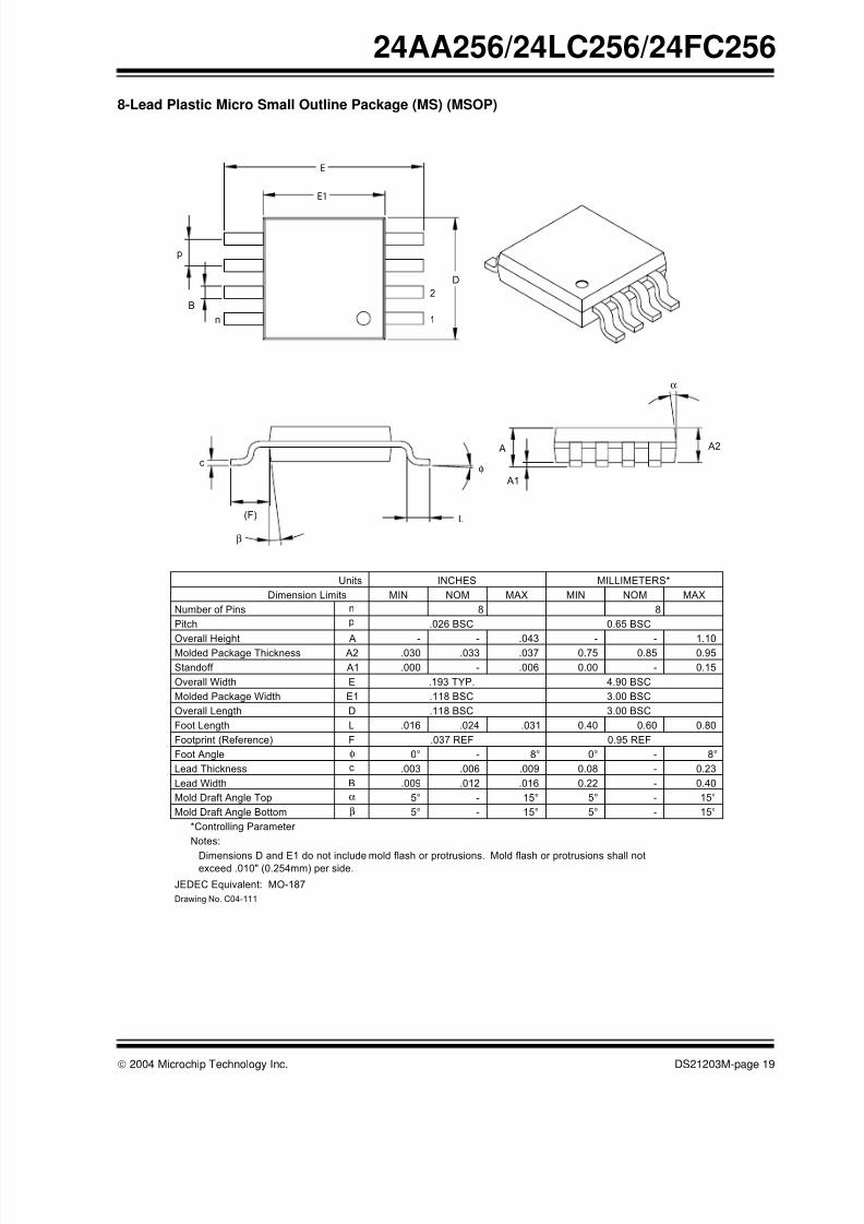
8-Lead Plastic Micro Small Outline Package (MS) (MSOP)
D
A
A1
L
c
(F)
α
A2
E1
E
p
B
n 1
2
φ
β
Dimensions D and E1 do not include mold flash or protrusions. Mold flash or protrusions shall not
.037 REFFFootprint (Reference)
exceed .010" (0.254mm) per side.
Notes:
Drawing No. C04-111
*Controlling Parameter
Mold Draft Angle Top
Mold Draft Angle Bottom
Foot Angle
Lead Width
Lead Thickness
β
α
c
B
φ
.003
.009
.006
.012
Dimension Limits
Overall HeightMolded Package Thickness
Molded Package Width
Overall Length
Foot Length
Standoff
Overall Width
Number of Pins
Pitch
A
L
E1
D
A1
E
A2
.016 .024
.118 BSC
.118 BSC
.000
.030
.193 TYP.
.033
MIN
p
n
Units
.026 BSC
NOM
8
INCHES
0.95 REF
-
-
.009
.016
0.08
0.22
0°
0.23
0.40
8°
MILLIMETERS*
0.65 BSC
0.85
3.00 BSC
3.00 BSC
0.60
4.90 BSC
.043
.031
.037
.006
0.40
0.00
0.75
MINMAX NOM
1.10
0.80
0.15
0.95
MAX
8
- -
-
15°5° -
15°5° -
JEDEC Equivalent: MO-187
0° - 8°
5°
5° -
-
15°
15°
--
- -
8/8/2019 i2c EEPROM 24xx256 Ds
http://slidepdf.com/reader/full/i2c-eeprom-24xx256-ds 20/28
24AA256/24LC256/24FC256
DS21203M-page 20 2004 Microchip Technology Inc.
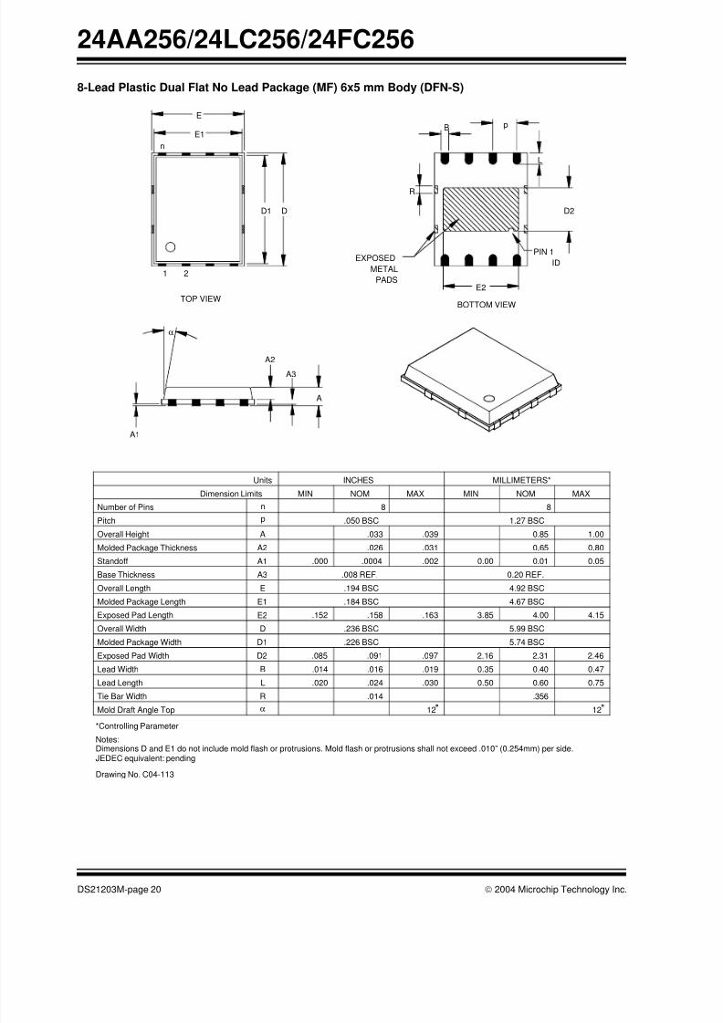
8-Lead Plastic Dual Flat No Lead Package (MF) 6x5 mm Body (DFN-S)
NOM
.050 BSC
INCHES
.194 BSC
.184 BSC
.226 BSC
.236 BSC
.008 REF.
DOverall Width
JEDEC equivalent: pending
Notes:
Drawing No. C04-113
Molded Package Width
Lead Width
*Controlling Parameter
Mold Draft Angle Top
Tie Bar Width
Lead Length
R
α
B
L
D1
.014
.020
Dimension Limits
Molded Package Thickness
Pitch
Overall Height
Overall Length
Molded Package Length
Base Thickness
Standoff
Number of Pins
A3
E1
E
A2
A1
A
.000
Units
n
p
MIN
TOP VIEW
1 2
A2
A
5.99 BSC
.019
12
.030
.014
.016
.024
0.35
0.50
.356
0.40
0.60
5.74 BSC
12
0.47
0.75
MILLIMETERS*
.039
.002
.031.026
.0004
.033
0.00
8
MAX MIN
1.27 BSC
0.20 REF.
4.92 BSC
4.67 BSC
0.85
0.01
0.65 0.80
0.05
1.00
MAXNOM
8
BOTTOM VIEW
n
E
E1
PIN 1
pB
Exposed Pad Length E2
Exposed Pad Width D2 .085 .091 .097 2.16 2.31 2.46
.152 .158 .163 3.85 4.00 4.15
EXPOSED
METAL
PADS
D2
E2
A1
A3
α
L
ID
D1 D
R
Dimensions D and E1 do not include mold flash or protrusions. Mold flash or protrusions shall not exceed .010” (0.254mm) per side.
8/8/2019 i2c EEPROM 24xx256 Ds
http://slidepdf.com/reader/full/i2c-eeprom-24xx256-ds 21/28
2004 Microchip Technology Inc. DS21203M-page 21
24AA256/24LC256/24FC256
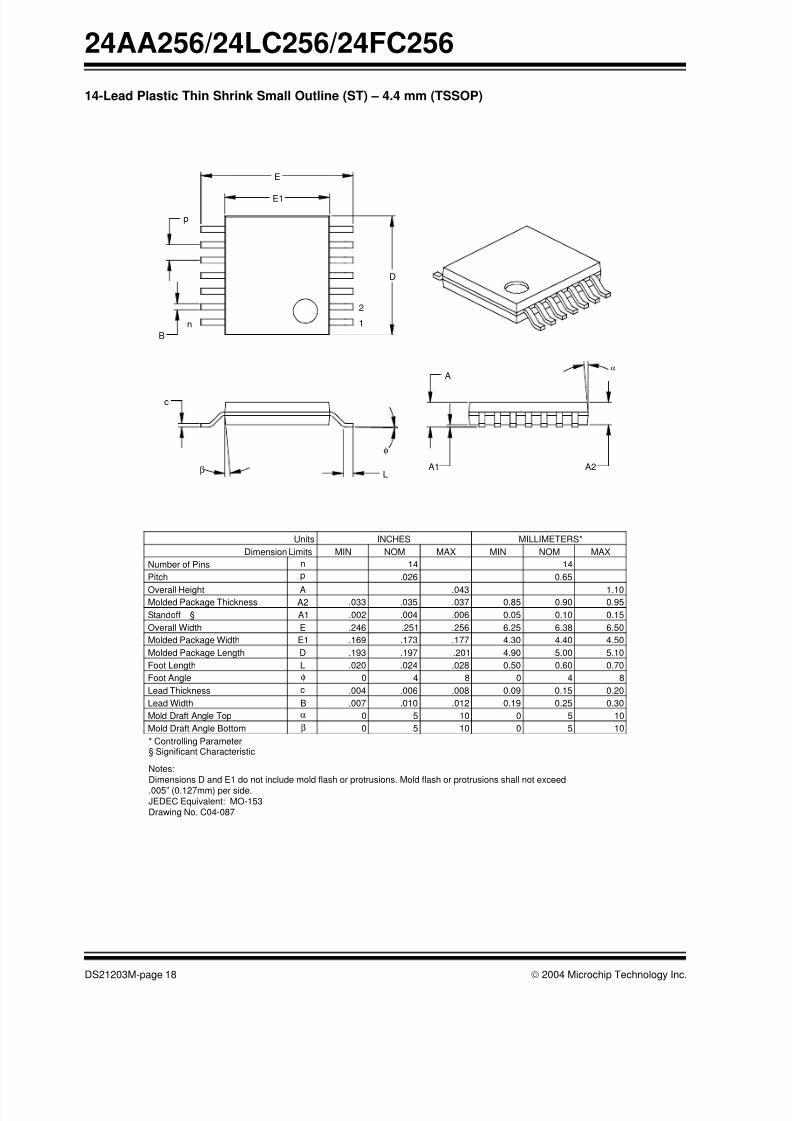
APPENDIX A: REVISION HISTORY
Revision L
Corrections to Section 1.0, Electrical Characteristics.
Revision M
Added 1.8V 400 kHz option for 24FC256.
8/8/2019 i2c EEPROM 24xx256 Ds
http://slidepdf.com/reader/full/i2c-eeprom-24xx256-ds 22/28
24AA256/24LC256/24FC256
DS21203M-page 22 2004 Microchip Technology Inc.
NOTES:
8/8/2019 i2c EEPROM 24xx256 Ds
http://slidepdf.com/reader/full/i2c-eeprom-24xx256-ds 23/28
2004 Microchip Technology Inc. DS21203M-page 23
24AA256/24LC256/24FC256
ON-LINE SUPPORT
Microchip provides on-line support on the Microchip
World Wide Web site.
The web site is used by Microchip as a means to make
files and information easily available to customers. To
view the site, the user must have access to the Internet
and a web browser, such as Netscape ® or Microsoft ®
Internet Explorer. Files are also available for FTP
download from our FTP site.
Connecting to the Microchip InternetWeb Site
The Microchip web site is available at the following
URL:
www.microchip.com
The file transfer site is available by using an FTP
service to connect to:
ftp://ftp.microchip.com
The web site and file transfer site provide a variety of
services. Users may download files for the latest
Development Tools, Data Sheets, Application Notes,
User's Guides, Articles and Sample Programs. A vari-
ety of Microchip specific business information is also
available, including listings of Microchip sales offices,
distributors and factory representatives. Other data
available for consideration is:
• Latest Microchip Press Releases
• Technical Support Section with Frequently Asked
Questions
• Design Tips
• Device Errata• Job Postings
• Microchip Consultant Program Member Listing
• Links to other useful web sites related to
Microchip Products
• Conferences for products, Development Systems,
technical information and more
• Listing of seminars and events
SYSTEMS INFORMATION ANDUPGRADE HOT LINE
The Systems Information and Upgrade Line provides
system users a listing of the latest versions of all of
Microchip's development systems software products.
Plus, this line provides information on how customers
can receive the most current upgrade kits. The Hot LineNumbers are:
1-800-755-2345 for U.S. and most of Canada, and
1-480-792-7302 for the rest of the world.
042003

8/8/2019 i2c EEPROM 24xx256 Ds
http://slidepdf.com/reader/full/i2c-eeprom-24xx256-ds 24/28
24AA256/24LC256/24FC256
DS21203M-page 24 2004 Microchip Technology Inc.
READER RESPONSE
It is our intention to provide you with the best documentation possible to ensure successful use of your Microchip prod-
uct. If you wish to provide your comments on organization, clarity, subject matter, and ways in which our documentation
can better serve you, please FAX your comments to the Technical Publications Manager at (480) 792-4150.
Please list the following information, and use this outline to provide us with your comments about this document.
To: Technical Publications Manager
RE: Reader Response
Total Pages Sent ________
From: Name
Company
Address
City / State / ZIP / Country
Telephone: (_______) _________ - _________
Application (optional):
Would you like a reply? Y N
Device: Literature Number:
Questions:
FAX: (______) _________ - _________
DS21203M24AA256/24LC256/24FC256
1. What are the best features of this document?
2. How does this document meet your hardware and software development needs?
3. Do you find the organization of this document easy to follow? If not, why?
4. What additions to the document do you think would enhance the structure and subject?
5. What deletions from the document could be made without affecting the overall usefulness?
6. Is there any incorrect or misleading information (what and where)?
7. How would you improve this document?
8/8/2019 i2c EEPROM 24xx256 Ds
http://slidepdf.com/reader/full/i2c-eeprom-24xx256-ds 25/28

8/8/2019 i2c EEPROM 24xx256 Ds
http://slidepdf.com/reader/full/i2c-eeprom-24xx256-ds 26/28
24AA256/24LC256/24FC256
DS21203M-page 26 2004 Microchip Technology Inc.
NOTES:
8/8/2019 i2c EEPROM 24xx256 Ds
http://slidepdf.com/reader/full/i2c-eeprom-24xx256-ds 27/28
2004 Microchip Technology Inc. DS21203M-page 27
Information contained in this publication regarding device
applications and the like is intended through suggestion only
and may be superseded by updates. It is your responsibility to
ensure that your application meets with your specifications.
No representation or warranty is given and no liability is
assumed by Microchip Technology Incorporated with respect
to the accuracy or use of such information, or infringement of
patents or other intellectual property rights arising from such
use or otherwise. Use of Microchip’s products as critical
components in life support systems is not authorized except
with express written approval by Microchip. No licenses are
conveyed, implicitly or otherwise, under any intellectual
property rights.
Trademarks
The Microchip name and logo, the Microchip logo, Accuron,
dsPIC, KEELOQ, microID, MPLAB, PIC, PICmicro, PICSTART,
PRO MATE, PowerSmart, rfPIC, and SmartShunt are
registered trademarks of Microchip Technology Incorporated
in the U.S.A. and other countries.
AmpLab, FilterLab, MXDEV, MXLAB, PICMASTER, SEEVAL,
SmartSensor and The Embedded Control Solutions Company
are registered trademarks of Microchip Technology
Incorporated in the U.S.A.
Analog-for-the-Digital Age, Application Maestro, dsPICDEM,
dsPICDEM.net, dsPICworks, ECAN, ECONOMONITOR,
FanSense, FlexROM, fuzzyLAB, In-Circuit SerialProgramming, ICSP, ICEPIC, Migratable Memory, MPASM,
MPLIB, MPLINK, MPSIM, PICkit, PICDEM, PICDEM.net,
PICLAB, PICtail, PowerCal, PowerInfo, PowerMate,
PowerTool, rfLAB, rfPICDEM, Select Mode, Smart Serial,
SmartTel and Total Endurance are trademarks of Microchip
Technology Incorporated in the U.S.A. and other countries.
SQTP is a service mark of Microchip Technology Incorporated
in the U.S.A.
All other trademarks mentioned herein are property of their
respective companies.
© 2004, Microchip Technology Incorporated, Printed in the
U.S.A., All Rights Reserved.
Printed on recycled paper.
Note the following details of the code protection feature on Microchip devices:
• Microchip products meet the specification contained in their particular Microchip Data Sheet.
• Microchip believes that its family of products is one of the most secure families of its kind on the market today, when used in the
intended manner and under normal conditions.
• There are dishonest and possibly illegal methods used to breach the code protection feature. All of these methods, to our
knowledge, require using the Microchip products in a manner outside the operating specifications contained in Microchip’s DataSheets. Most likely, the person doing so is engaged in theft of intellectual property.
• Microchip is willing to work with the customer who is concerned about the integrity of their code.
• Neither Microchip nor any other semiconductor manufacturer can guarantee the security of their code. Code protection does not
mean that we are guaranteeing the product as “unbreakable.”
Code protection is constantly evolving. We at Microchip are committed to continuously improving the code protection features of our
products. Attempts to break Microchip’s code protection feature may be a violation of the Digital Millennium Copyright Act. If such acts
allow unauthorized access to your software or other copyrighted work, you may have a right to sue for relief under that Act.
Microchip received ISO/TS-16949:2002 quality system certification for its worldwide headquarters, design and wafer fabrication facilities in Chandler and Tempe, Arizona and Mountain View, California in October 2003. The Company’s quality system processes and procedures are for its PICmicro ® 8-bit MCUs, K EE LOQ ® code hopping devices, Serial EEPROMs, microperipherals, nonvolatile memory and analog products. In addition, Microchip’s quality system for the design and manufacture of development systems is ISO 9001:2000 certified.
8/8/2019 i2c EEPROM 24xx256 Ds
http://slidepdf.com/reader/full/i2c-eeprom-24xx256-ds 28/28
AMERICAS
Corporate Office2355 West Chandler Blvd.Chandler, AZ 85224-6199Tel: 480-792-7200Fax: 480-792-7277Technical Support: 480-792-7627Web Address: www.microchip.com
Atlanta3780 Mansell Road, Suite 130Alpharetta, GA 30022Tel: 770-640-0034Fax: 770-640-0307
Boston2 Lan Drive, Suite 120Westford, MA 01886Tel: 978-692-3848Fax: 978-692-3821
Chicago333 Pierce Road, Suite 180Itasca, IL 60143Tel: 630-285-0071Fax: 630-285-0075
Dallas4570 Westgrove Drive, Suite 160Addison, TX 75001Tel: 972-818-7423Fax: 972-818-2924
DetroitTri-Atria Office Building32255 Northwestern Highway, Suite 190Farmington Hills, MI 48334Tel: 248-538-2250Fax: 248-538-2260
Kokomo2767 S. Albright RoadKokomo, IN 46902Tel: 765-864-8360Fax: 765-864-8387
Los Angeles18201 Von Karman, Suite 1090Irvine, CA 92612Tel: 949-263-1888Fax: 949-263-1338
San Jose1300 Terra Bella AvenueMountain View, CA 94043Tel: 650-215-1444Fax: 650-961-0286
Toronto6285 Northam Drive, Suite 108
Mississauga, Ontario L4V 1X5, CanadaTel: 905-673-0699Fax: 905-673-6509
ASIA/PACIFIC
AustraliaSuite 22, 41 Rawson StreetEpping 2121, NSWAustraliaTel: 61-2-9868-6733Fax: 61-2-9868-6755
China - BeijingUnit 706BWan Tai Bei Hai Bldg.No. 6 Chaoyangmen Bei Str.Beijing, 100027, ChinaTel: 86-10-85282100Fax: 86-10-85282104
China - ChengduRm. 2401-2402, 24th Floor,Ming Xing Financial TowerNo. 88 TIDU StreetChengdu 610016, ChinaTel: 86-28-86766200Fax: 86-28-86766599
China - FuzhouUnit 28F, World Trade PlazaNo. 71 Wusi Road
Fuzhou 350001, ChinaTel: 86-591-7503506Fax: 86-591-7503521
China - Hong Kong SARUnit 901-6, Tower 2, Metroplaza223 Hing Fong RoadKwai Fong, N.T., Hong KongTel: 852-2401-1200Fax: 852-2401-3431
China - ShanghaiRoom 701, Bldg. BFar East International PlazaNo. 317 Xian Xia RoadShanghai, 200051Tel: 86-21-6275-5700Fax: 86-21-6275-5060
China - ShenzhenRm. 1812, 18/F, Building A, United Plaza
No. 5022 Binhe Road, Futian DistrictShenzhen 518033, ChinaTel: 86-755-82901380Fax: 86-755-8295-1393
China - ShundeRoom 401, Hongjian Building, No. 2Fengxiangnan Road, Ronggui Town, ShundeDistrict, Foshan City, Guangdong 528303, ChinaTel: 86-757-28395507 Fax: 86-757-28395571
China - QingdaoRm. B505A, Fullhope Plaza,No. 12 Hong Kong Central Rd.Qingdao 266071, ChinaTel: 86-532-5027355 Fax: 86-532-5027205
IndiaDivyasree Chambers1 Floor, Wing A (A3/A4)No. 11, O’Shaugnessey RoadBangalore, 560 025, IndiaTel: 91-80-22290061 Fax: 91-80-22290062
JapanBenex S-1 6F3-18-20, ShinyokohamaKohoku-Ku, Yokohama-shiKanagawa, 222-0033, JapanTel: 81-45-471- 6166 Fax: 81-45-471-6122
Korea168-1, Youngbo Bldg. 3 FloorSamsung-Dong, Kangnam-KuSeoul, Korea 135-882Tel: 82-2-554-7200 Fax: 82-2-558-5932 or82-2-558-5934
Singapore200 Middle Road#07-02 Prime CentreSingapore, 188980Tel: 65-6334-8870 Fax: 65-6334-8850
TaiwanKaohsiung Branch30F - 1 No. 8Min Chuan 2nd RoadKaohsiung 806, TaiwanTel: 886-7-536-4818Fax: 886-7-536-4803
TaiwanTaiwan Branch11F-3, No. 207Tung Hua North RoadTaipei, 105, TaiwanTel: 886-2-2717-7175 Fax: 886-2-2545-0139
EUROPEAustriaDurisolstrasse 2A-4600 WelsAustriaTel: 43-7242-2244-399Fax: 43-7242-2244-393
DenmarkRegus Business CentreLautrup hoj 1-3Ballerup DK-2750 Denmark
Tel: 45-4420-9895 Fax: 45-4420-9910FranceParc d’Activite du Moulin de Massy43 Rue du Saule TrapuBatiment A - ler Etage91300 Massy, FranceTel: 33-1-69-53-63-20Fax: 33-1-69-30-90-79
GermanySteinheilstrasse 10D-85737 Ismaning, GermanyTel: 49-89-627-144-0Fax: 49-89-627-144-44
ItalyVia Quasimodo, 1220025 Legnano (MI)Milan, ItalyTel: 39-0331-742611
Fax: 39-0331-466781NetherlandsWaegenburghtplein 4NL-5152 JR, Drunen, NetherlandsTel: 31-416-690399Fax: 31-416-690340
United Kingdom505 Eskdale RoadWinnersh TriangleWokinghamBerkshire, England RG41 5TUTel: 44-118-921-5869Fax: 44-118-921-5820
05/28/04
WORLDWIDE SALES AND SERVICE