Hx 2615541560
8
Thummuru Siddartha Reddy, Bellamkonda Saikrishna Vyas, Thota Avinash, Thumati Ravi / International Journal of Engineering Research and Applications (IJERA) ISSN: 2248-9622 www.ijera.com Vol. 2, Issue 6, November- December 2012, pp.1554-1560 1554 | P a g e Comparision Of Different Parameters On Cpw Fed Bowtie Antenna Thummuru Siddartha Reddy * , Bellamkonda Saikrishna Vyas ** , Thota Avinash**, Thumati Ravi *** [*][**] Final Year B.Tech, Dept. Of Ece, Kl University, Vaddeswaram, Ap, India [***] Associate Professor B.Tech, Dept. Of Ece, Kl University, Vaddeswaram, Ap, India Abstract Here we used a lumped port excitation for the Co-Planar Waveguide (CPW) feed. We used copper cladding for cutout and for substrate dielectric material named Arlon Cu Clad 217(tm).The CPW slots and antenna shape acts as openings in a metallized plane. The antenna has been analyzed over frequency ranges of S- band (2.20-3.95(GHz)), C-band(4.90-8.20(GHz)) andX-band (8.20-12.40(GHz)).Their return loss, gain, directivity, VSWR and impedances have been compared. It is covered with air box depending on the minimum distance between the air wall and the radiating aperture at the starting frequency i.e., (9.375mm).Though experiments with bow-tie antennas of various extended angles, the bow-tie antenna with a 90 0 extended angle exhibits the widest bandwidth in the desired frequency band which has a bandwidth of 25% for a VSWR <1.5:1, 16.96% for a VSWR <1.2:1 and 9.19% for a VSWR <1.4:1 Key words: CPW, Bow-Tie, Return loss, Gain, Directivity, VSWR Introduction: Printed slot antennas fed by coplanar waveguide (CPW) have many pros over microstrip antennas. Apart from small size, light weight, low cost, good performance, ease of fabrication and installation, and low profile, they expose wider bandwidth, lower dispersion and lower radiation loss than microstripantennas besides the ease of being shunted with active and passive elements required for matching and gain improvement . Bow- Tie and bow-tie slot antennas are good performers for wideband applications. Generally waveguide refers to any linear structure that conveys electromagnetic waves between its end points. Most commonly is a hollow metal pipe used to carry radio waves. So, this type of wave guide is used as a transmission line mostly at microwave frequencies, for such purposes as connecting microwave transmitters and receivers to their antennas, in equipment such as microwave ovens, radar sets, satellite communications, and microwave radio links. The electromagnetic waves in waveguide travel down the guide in a zig-zag path, being repeatedly reflected between opposite walls of the guide. In this paper, bow-tie slot antenna geometry with lumped port feed is studied and designed for wideband applications. The related simulation and analysis are performed using the using BGA, QFP, Flip-Chip package, Ansoft HFSS. This is based on Finite Element Method (FEM), adaptive meshing to give unparalleled performance. This is integrated with simulation, visualization, solid modeling and automation. This can calculate parameters such as S-parameters, Resonant Frequency, and Fields. Element Geometry and Analysis : The geometry of the CPW fed bowtie antenna is shown in Fig. 1. The tapering from the CPW to the bow-tie slot is to achieve better matching with lumped port. The antenna is studied for 2mm substrate with ε r = 2.17 and to create a ground for substrate we use copper cladding as its dielectric material in XY-plane.We assign a finite conductivity boundary to the copper cladding. Then we create Feed cut out with dimensions 13mm X 0.6mm and later we create bowtie arms, unite them. Then we take mirror image of it and create two bowtie arms. Next we have subtracted the Bowtie from the cladding and then assign a mesh operation on the bowtie along the length. Then assign lumped port excitation with resistance 50 ohm and reactance 0 ohm with a single mode. The analysis is performed between various frequency bands but we consider better air volume which suits better i.e., 8-12 GHz. Therefore the minimum distance between the air volume wall and the radiating aperture should be one quarter wavelength at 8 GHz, or 0.25(c/f) =9.375mm.The dimension is rounded to 9.5mm spacing.
-
Upload
anonymous-7vppkws8o -
Category
Documents
-
view
225 -
download
0
Transcript of Hx 2615541560

7/30/2019 Hx 2615541560
http://slidepdf.com/reader/full/hx-2615541560 1/7
Thummuru Siddartha Reddy, Bellamkonda Saikrishna Vyas, Thota Avinash, Thumati Ravi /
International Journal of Engineering Research and Applications (IJERA)
ISSN: 2248-9622 www.ijera.com Vol. 2, Issue 6, November- December 2012, pp.1554-1560
1554 | P a g e
Comparision Of Different Parameters On Cpw Fed Bowtie
Antenna
Thummuru Siddartha Reddy* , Bellamkonda Saikrishna Vyas**, Thota
Avinash**, Thumati Ravi***
[*][**] Final Year B.Tech, Dept. Of Ece, Kl University, Vaddeswaram, Ap, India[***]
Associate Professor B.Tech, Dept. Of Ece, Kl University, Vaddeswaram, Ap, India
AbstractHere we used a lumped port excitation
for the Co-Planar Waveguide (CPW) feed. We
used copper cladding for cutout and for substrate
dielectric material named Arlon Cu Clad217(tm).The CPW slots and antenna shape acts
as openings in a metallized plane. The antenna
has been analyzed over frequency ranges of S-
band (2.20-3.95(GHz)), C-band(4.90-8.20(GHz))
andX-band (8.20-12.40(GHz)).Their return loss,
gain, directivity, VSWR and impedances have
been compared. It is covered with air box
depending on the minimum distance between the
air wall and the radiating aperture at the starting
frequency i.e., (9.375mm).Though experiments
with bow-tie antennas of various extended angles,
the bow-tie antenna with a 900 extended angle
exhibits the widest bandwidth in the desiredfrequency band which has a bandwidth of 25%
for a VSWR <1.5:1, 16.96% for a VSWR <1.2:1
and 9.19% for a VSWR <1.4:1
Key words: CPW, Bow-Tie, Return loss, Gain,
Directivity, VSWR
Introduction:Printed slot antennas fed by coplanar
waveguide (CPW) have many pros over microstrip
antennas. Apart from small size, light weight, low
cost, good performance, ease of fabrication and
installation, and low profile, they expose widerbandwidth, lower dispersion and lower radiation
loss than microstripantennas besides the ease of
being shunted with active and passive elements
required for matching and gain improvement . Bow-
Tie and bow-tie slot antennas are good performers
for wideband applications.
Generally waveguide refers to any linear
structure that conveys electromagnetic waves
between its end points. Most commonly is a hollowmetal pipe used to carry radio waves. So, this type
of wave guide is used as a transmission line mostly
at microwave frequencies, for such purposes as
connecting microwave transmitters and receivers totheir antennas, in equipment such as microwave
ovens, radar sets, satellite communications, and
microwave radio links. The electromagnetic waves
in waveguide travel down the guide in a zig-zag
path, being repeatedly reflected between opposite
walls of the guide.
In this paper, bow-tie slot antennageometry with lumped port feed is studied and
designed for wideband applications. The related
simulation and analysis are performed using the
using BGA, QFP, Flip-Chip package, Ansoft
HFSS. This is based on Finite Element Method
(FEM), adaptive meshing to give unparalleledperformance. This is integrated with simulation,
visualization, solid modeling and automation. This
can calculate parameters such as S-parameters,
Resonant Frequency, and Fields.
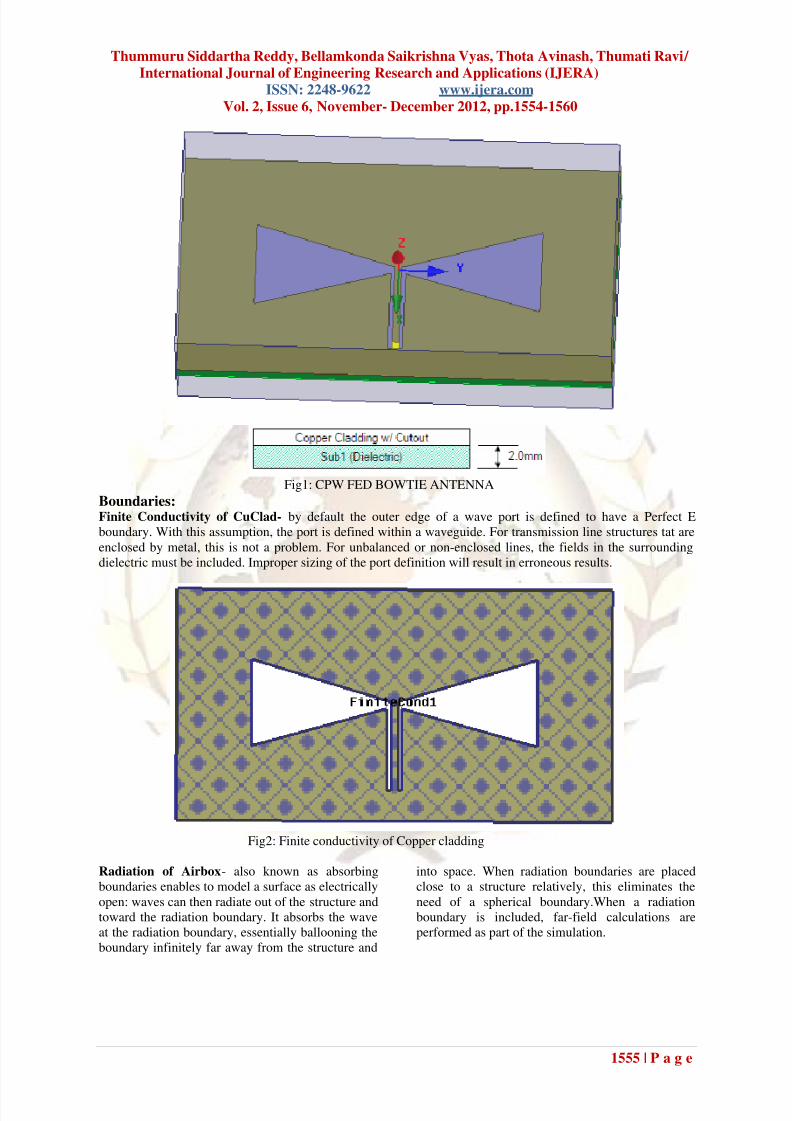
Element Geometry and Analysis:The geometry of the CPW fed bowtie
antenna is shown in Fig. 1. The tapering from the
CPW to the bow-tie slot is to achieve better
matching with lumped port. The antenna is studied
for 2mm substrate with εr = 2.17 and to create a
ground for substrate we use copper cladding as its
dielectric material in XY-plane.We assign a finite
conductivity boundary to the copper cladding. Thenwe create Feed cut out with dimensions 13mm X
0.6mm and later we create bowtie arms, unite them.
Then we take mirror image of it and create two
bowtie arms. Next we have subtracted the Bowtiefrom the cladding and then assign a mesh operation
on the bowtie along the length. Then assign lumpedport excitation with resistance 50 ohm and reactance
0 ohm with a single mode.
The analysis is performed between various
frequency bands but we consider better air volume
which suits better i.e., 8-12 GHz. Therefore the
minimum distance between the air volume wall and
the radiating aperture should be one quarter
wavelength at 8 GHz, or 0.25(c/f) =9.375mm.The
dimension is rounded to 9.5mm spacing.
7/30/2019 Hx 2615541560
http://slidepdf.com/reader/full/hx-2615541560 2/7
Thummuru Siddartha Reddy, Bellamkonda Saikrishna Vyas, Thota Avinash, Thumati Ravi /
International Journal of Engineering Research and Applications (IJERA)
ISSN: 2248-9622 www.ijera.com Vol. 2, Issue 6, November- December 2012, pp.1554-1560
1555 | P a g e
Fig1: CPW FED BOWTIE ANTENNA
Boundaries:Finite Conductivity of CuClad- by default the outer edge of a wave port is defined to have a Perfect E
boundary. With this assumption, the port is defined within a waveguide. For transmission line structures tat are
enclosed by metal, this is not a problem. For unbalanced or non-enclosed lines, the fields in the surrounding
dielectric must be included. Improper sizing of the port definition will result in erroneous results.
Fig2: Finite conductivity of Copper cladding
Radiation of Airbox- also known as absorbing
boundaries enables to model a surface as electrically
open: waves can then radiate out of the structure and
toward the radiation boundary. It absorbs the wave
at the radiation boundary, essentially ballooning the
boundary infinitely far away from the structure and
into space. When radiation boundaries are placed
close to a structure relatively, this eliminates the
need of a spherical boundary.When a radiation
boundary is included, far-field calculations are
performed as part of the simulation.
7/30/2019 Hx 2615541560
http://slidepdf.com/reader/full/hx-2615541560 3/7
Thummuru Siddartha Reddy, Bellamkonda Saikrishna Vyas, Thota Avinash, Thumati Ravi /
International Journal of Engineering Research and Applications (IJERA)
ISSN: 2248-9622 www.ijera.com Vol. 2, Issue 6, November- December 2012, pp.1554-1560
1556 | P a g e
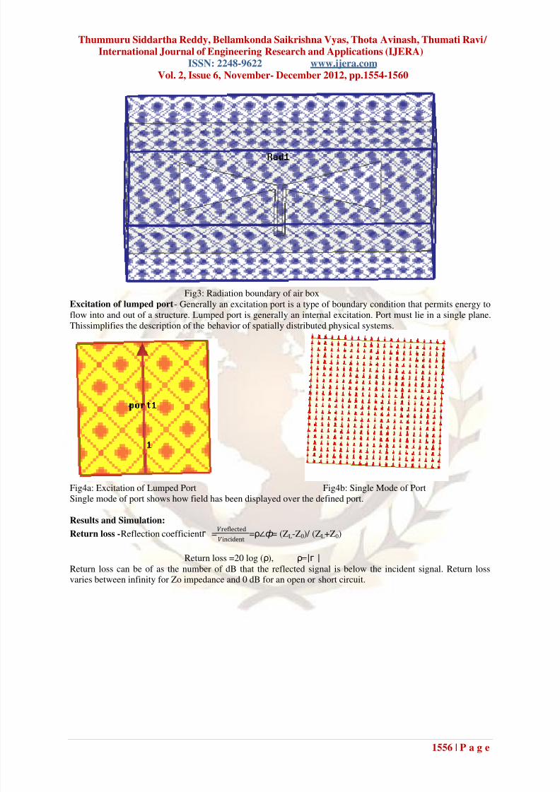
Fig3: Radiation boundary of air box
Excitation of lumped port- Generally an excitation port is a type of boundary condition that permits energy to
flow into and out of a structure. Lumped port is generally an internal excitation. Port must lie in a single plane.
Thissimplifies the description of the behavior of spatially distributed physical systems.
Fig4a: Excitation of Lumped Port Fig4b: Single Mode of Port
Single mode of port shows how field has been displayed over the defined port.
Results and Simulation:
Return loss -Reflection coefficientᴦ =reflected
incident =ρ∠ф= (ZL-Z0)/ (ZL+Z0)
Return loss =20 log (ρ), ρ=ᴦ Return loss can be of as the number of dB that the reflected signal is below the incident signal. Return lossvaries between infinity for Zo impedance and 0 dB for an open or short circuit.
7/30/2019 Hx 2615541560
http://slidepdf.com/reader/full/hx-2615541560 4/7
Thummuru Siddartha Reddy, Bellamkonda Saikrishna Vyas, Thota Avinash, Thumati Ravi /
International Journal of Engineering Research and Applications (IJERA)
ISSN: 2248-9622 www.ijera.com Vol. 2, Issue 6, November- December 2012, pp.1554-1560
1557 | P a g e
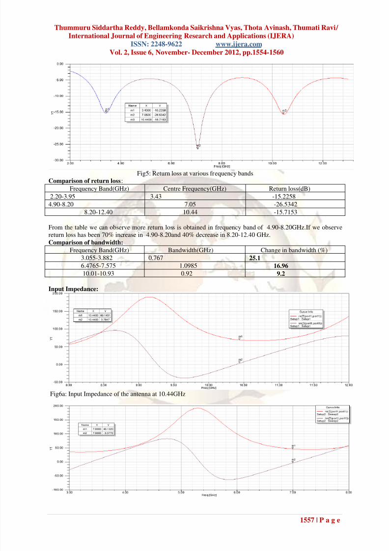
Fig5: Return loss at various frequency bands
Comparison of return loss:
Frequency Band(GHz) Centre Frequency(GHz) Return loss(dB)
2.20-3.95 3.43 -15.2258
4.90-8.20 7.05 -26.5342
8.20-12.40 10.44 -15.7153
From the table we can observe more return loss is obtained in frequency band of 4.90-8.20GHz.If we observe
return loss has been 70% increase in 4.90-8.20and 40% decrease in 8.20-12.40 GHz.
Comparison of bandwidth:
Frequency Band(GHz) Bandwidth(GHz) Change in bandwidth (%)
3.055-3.882 0.767 25.1
6.4765-7.575 1.0985 16.96
10.01-10.93 0.92 9.2
Input Impedance:
Fig6a: Input Impedance of the antenna at 10.44GHz
7/30/2019 Hx 2615541560
http://slidepdf.com/reader/full/hx-2615541560 5/7
Thummuru Siddartha Reddy, Bellamkonda Saikrishna Vyas, Thota Avinash, Thumati Ravi /
International Journal of Engineering Research and Applications (IJERA)
ISSN: 2248-9622 www.ijera.com Vol. 2, Issue 6, November- December 2012, pp.1554-1560
1558 | P a g e
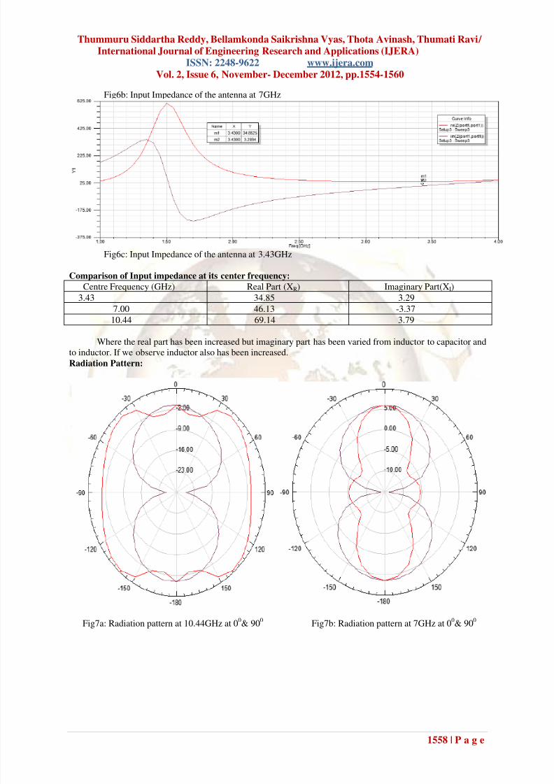
Fig6b: Input Impedance of the antenna at 7GHz
Fig6c: Input Impedance of the antenna at 3.43GHz
Comparison of Input impedance at its center frequency:Centre Frequency (GHz) Real Part (XR) Imaginary Part(XI)
3.43 34.85 3.29
7.00 46.13 -3.37
10.44 69.14 3.79
Where the real part has been increased but imaginary part has been varied from inductor to capacitor and
to inductor. If we observe inductor also has been increased.
Radiation Pattern:
Fig7a: Radiation pattern at 10.44GHz at 00& 90
0Fig7b: Radiation pattern at 7GHz at 0
0& 90
0

7/30/2019 Hx 2615541560
http://slidepdf.com/reader/full/hx-2615541560 6/7
Thummuru Siddartha Reddy, Bellamkonda Saikrishna Vyas, Thota Avinash, Thumati Ravi /
International Journal of Engineering Research and Applications (IJERA)
ISSN: 2248-9622 www.ijera.com Vol. 2, Issue 6, November- December 2012, pp.1554-1560
1559 | P a g e
Fig7c: Radiation pattern at 3.43GHz at 00& 900 From Fig7a, Fig7b, Fig7c we observed that directivity has been increased as frequency increased which is
happened in Fig7b and Fig7c we want even coverage area to be increased which is happened in Fig7a.
Gain(dB):
Fig8a: Gain at 8.20-12.20GHz Fig8b: Gain at 4.90-8.20GHz Fig8c: Gain at 2.20- 3.95GHz
VSWR:
Fig9: VSWR of all three frequency bands considered

7/30/2019 Hx 2615541560
http://slidepdf.com/reader/full/hx-2615541560 7/7
Thummuru Siddartha Reddy, Bellamkonda Saikrishna Vyas, Thota Avinash, Thumati Ravi /
International Journal of Engineering Research and Applications (IJERA)
ISSN: 2248-9622 www.ijera.com Vol. 2, Issue 6, November- December 2012, pp.1554-1560
1560 | P a g e
ConclusionFrom the simulated results we can observe
that input impedance of three frequency bands are
34.85+i3.29, 46.13-i3.37, 69.14+i3.79 from the fig:6a, 6b&6c. VSWR ranges differently at threefrequency bands 1.4:1, 1.11:1, and
1.38:1.Directivity at their center frequencies and
phi values 0deg and 90deg has been improved but
more area is being covered at 10.44GHz.Finaly,
gain in 2.90-3.95GHz is -2.83dB, in 4.90-8.20GHz
is 6.03dB and in 8.20-12.40 GHz we have4.36dB.We can observe more uniformity in 3-
5GHz but we get negative gain. From all the results
we observed that it gives better performance in 5.5-
7.5 and 8-12GHz frequency bands but bandwidth
has been more in 2.90-3.95GHz and next to it was
4.9-8.20 GHz. Therefore, this model performs wellin 4.9-8.20 GHz.
References 1. A.Harish Babu, P.Ashesh Babu, E.Vamsi
Krishna IETE Members and Research
students in kl-university.
2. C. Balanis, Antenna Theory, Analysis and
Design, 3rd edition, New York: Wiley,
2005. 2.3. HFSS hand book for excitations and
boundary conditions.
4. C. Balanis, Antenna Theory, Analysis and
Design, 3rd edition, New York: Wiley,
2005.
5. HFSS hand book for excitations andboundary conditions.
6. E. J. Candes, M. B. Wakin, and S. P.
Boyd, “Enhancing sparsity by reweighted
minimization,”Fourier Analysis Applica.,
vol. 14, pp.877 – 905, Oct. 2008.
7. O. M. Bucci, C. Gennarelli, and C.
Savarese, “Representation of
electromagnetic fields over
BIOGRAPHY:
Thummuru Siddartha Reddy*
was born in 1992 at Guntur
district. He is currently pursuing
B.Tech from K L University. He
is interested in Wireless systems
and Telecommunication.
Email:[email protected]
Bellamkonda Saikrishna
Vyas**
was born in 1992in,Guntur district. He is
pursuing his B.tech from K LUniversity. He is interested in
Communications and Wireless
Networks.
Email:[email protected]
Thota Avinash**was born in
1991 at Vijayawada. He is
now pursuing B.Tech Degree
in Electronics &
Communication Engineering
In K L University. He is
interested in Communication and Networking.
Email:[email protected]
Thumati Ravi*** is workingas Associate Proffesor in KL
University. He is interested in
Image Processing.
Email: [email protected]
Correspondence author: Thummuru Siddartha
Reddy,[email protected],ph
no:+919701740343.