Fundamentals of Semiconductor Physics 万 歆 Zhejiang Institute of Modern Physics...
76
Fundamentals of Semiconductor Physics 万 万 Zhejiang Institute of Modern Physics [email protected] http://zimp.zju.edu.cn/~xinwan/ Fall 2006
-
Upload
charity-blair -
Category
Documents
-
view
238 -
download
1
Transcript of Fundamentals of Semiconductor Physics 万 歆 Zhejiang Institute of Modern Physics...
Fundamentals of Semiconductor Physics
万 歆Zhejiang Institute of Modern Physics
http://zimp.zju.edu.cn/~xinwan/
Fall 2006
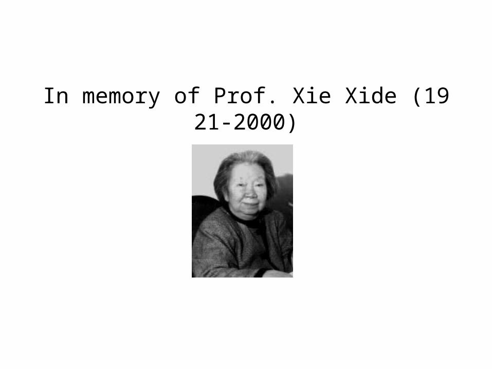
In memory of Prof. Xie Xide (1921-2000)
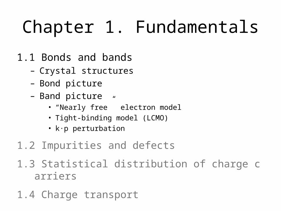
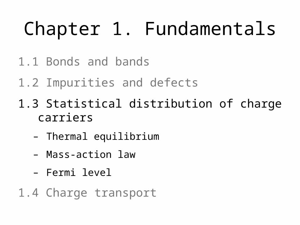
Chapter 1. Fundamentals
1.1 Bonds and bands
1.2 Impurities and defects
1.3 Statistical distribution of charge carriers
1.4 Charge transport
Total 12 hours.
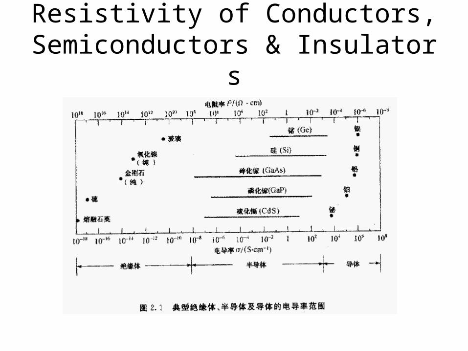
Resistivity of Conductors, Semiconductors & Insulators
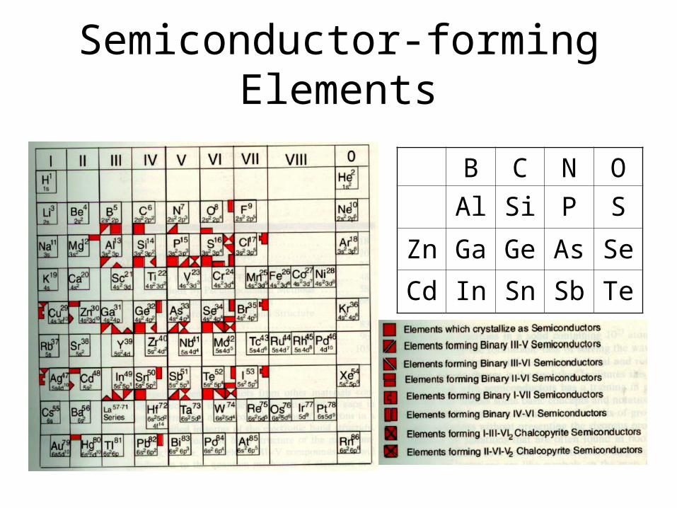
Semiconductor-forming Elements
B C N O
Al Si P S
Zn Ga Ge As Se
Cd In Sn Sb Te
Chapter 1. Fundamentals
1.1 Bonds and bands– Crystal structures– Bond picture– Band picture
• “Nearly free” electron model• Tight-binding model (LCMO)• k·p perturbation
1.2 Impurities and defects
1.3 Statistical distribution of charge carriers
1.4 Charge transport
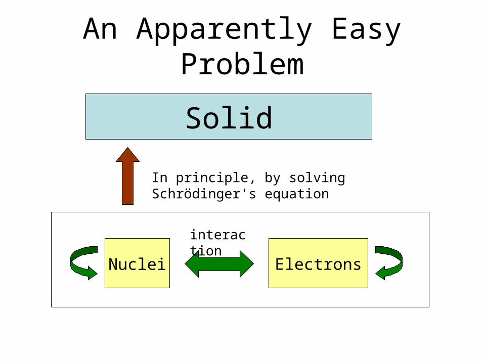
An Apparently Easy Problem
Solid
Nuclei Electrons
interaction
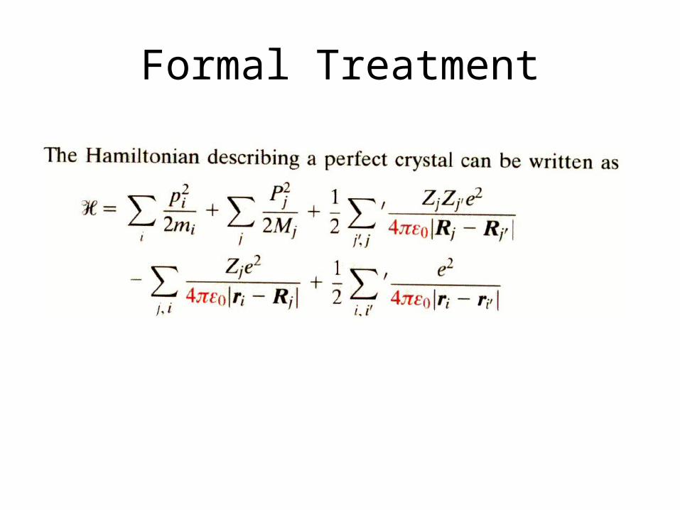
In principle, by solving Schrödinger's equation
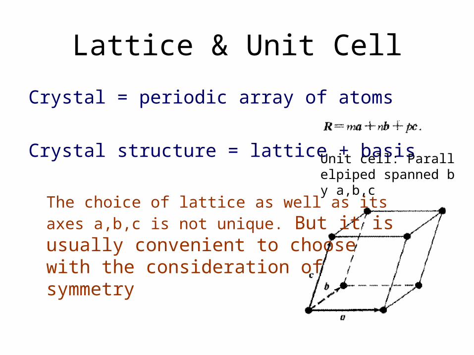
Lattice & Unit Cell
Crystal = periodic array of atoms
Crystal structure = lattice + basis
The choice of lattice as well as its axes a,b,c is not unique. But it is usually convenient to choose with the consideration of symmetry
Unit cell: Parallelpiped spanned by a,b,c
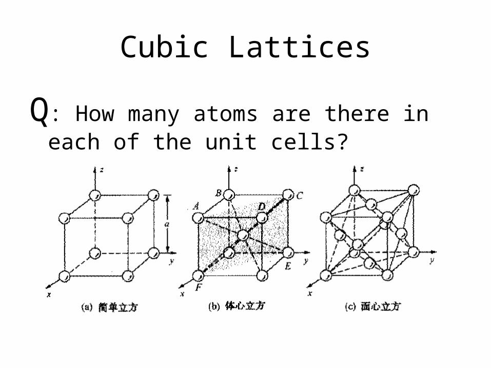
Cubic Lattices
Q: How many atoms are there in each of the unit cells?
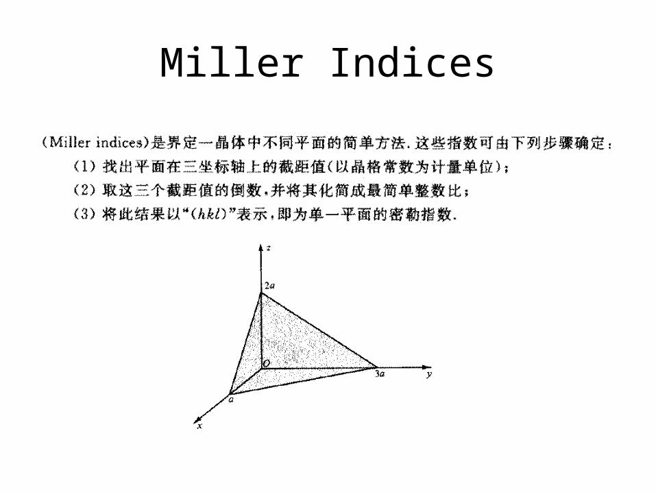
Miller Indices
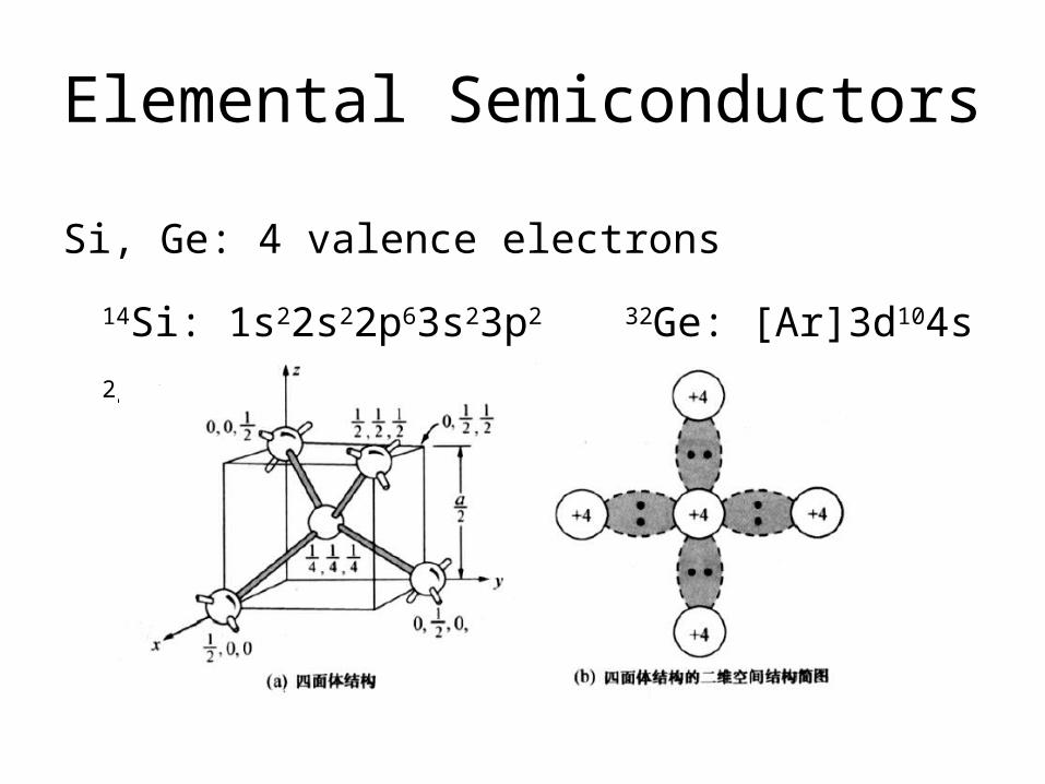
Elemental Semiconductors
Si, Ge: 4 valence electrons
14Si: 1s22s22p63s23p2 32Ge: [Ar]3d104s24p2
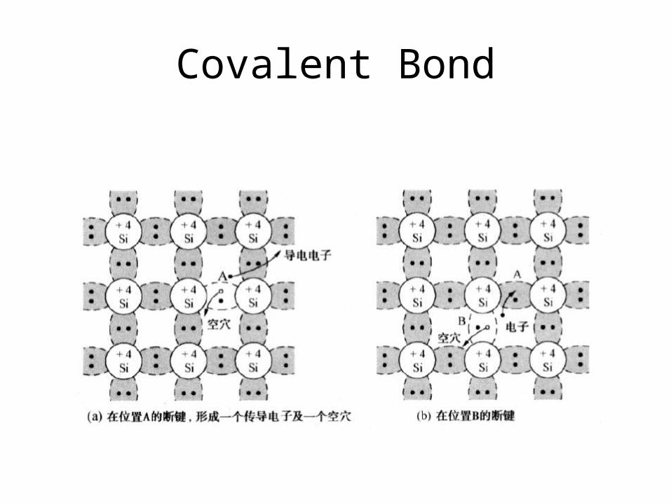
Covalent Bond
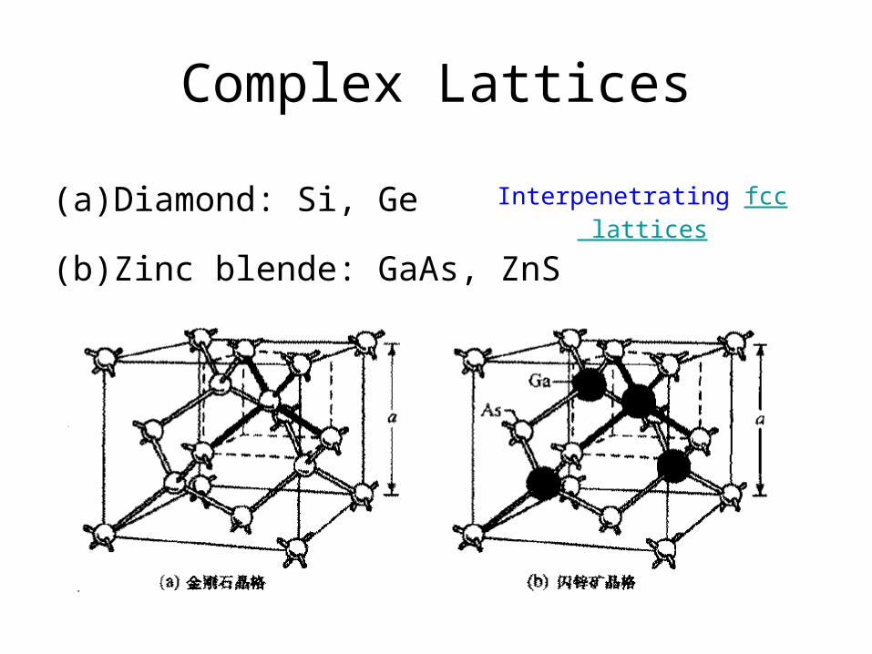
Complex Lattices
(a) Diamond: Si, Ge
(b) Zinc blende: GaAs, ZnS
Interpenetrating fcc lattices
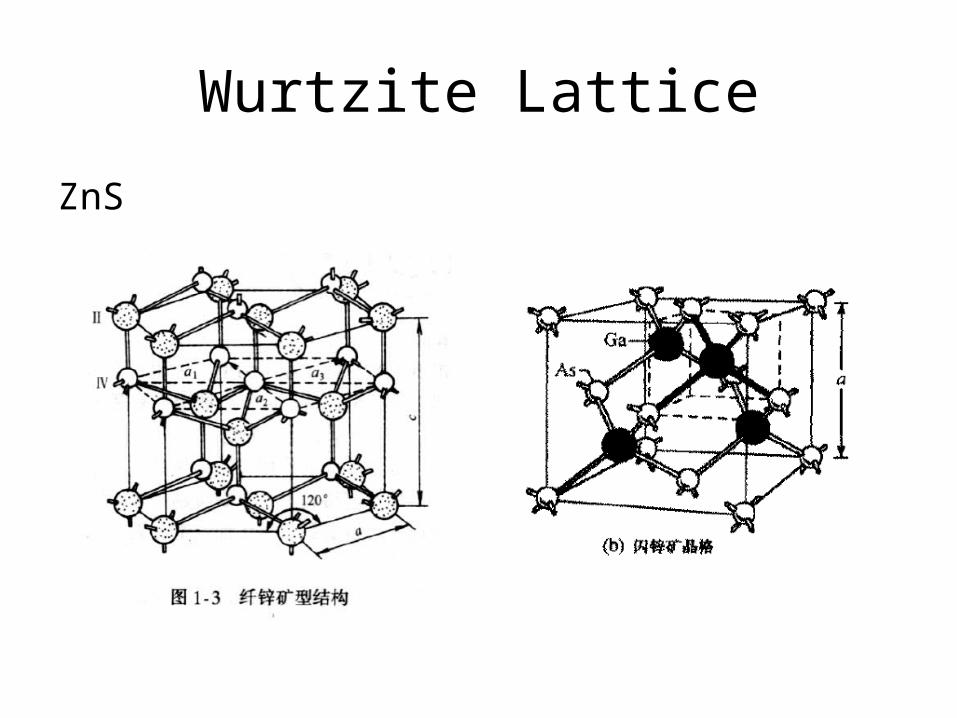
Wurtzite Lattice
ZnS
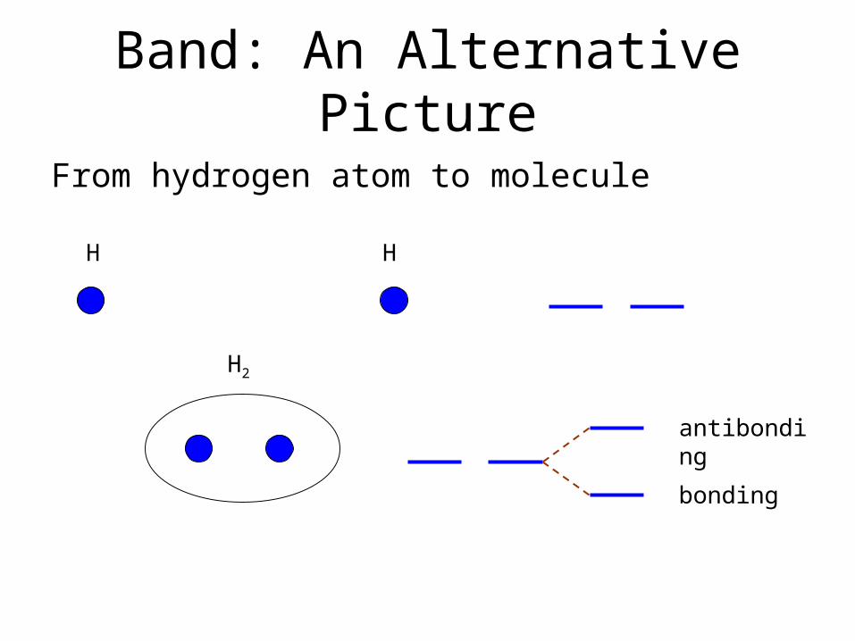
Band: An Alternative Picture
From hydrogen atom to molecule
H H
H2
bonding
antibonding
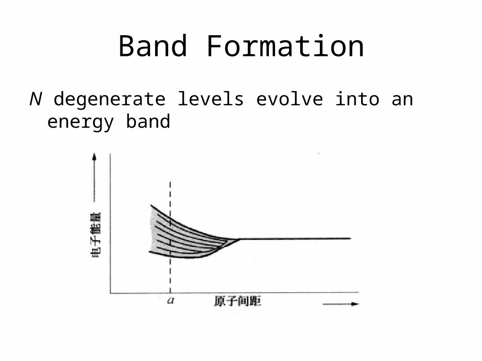
Band Formation
N degenerate levels evolve into an energy band
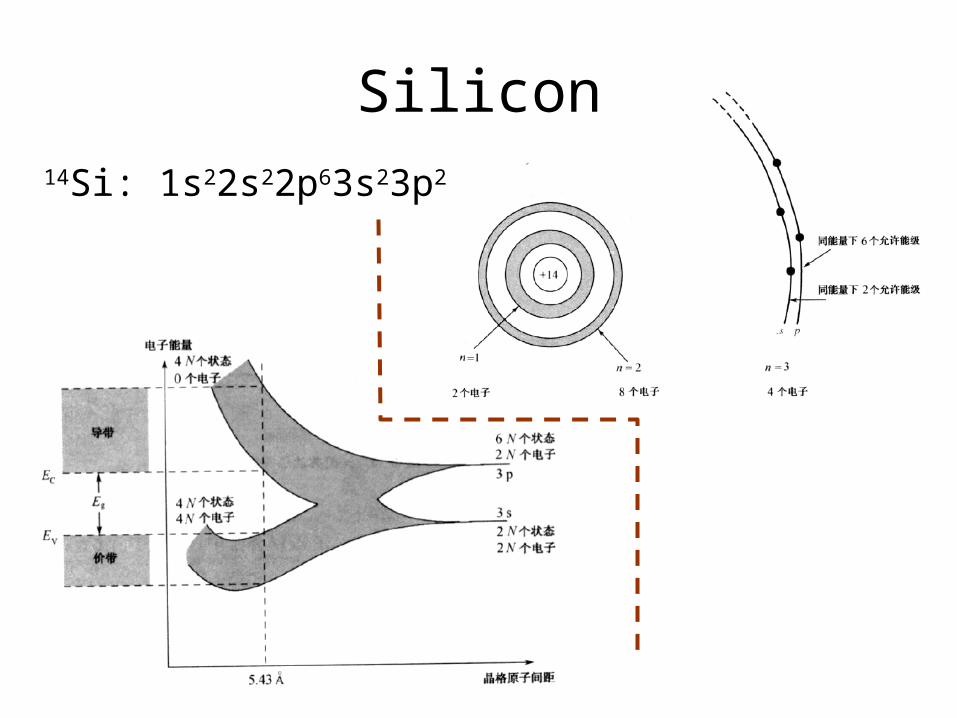
Silicon14Si: 1s22s22p63s23p2
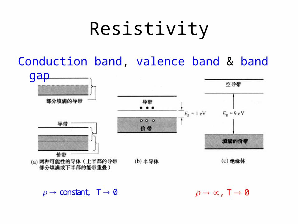
Resistivity
Conduction band, valence band & band gap
constant, T 0 , T 0
Formal Treatment
Approximation 1
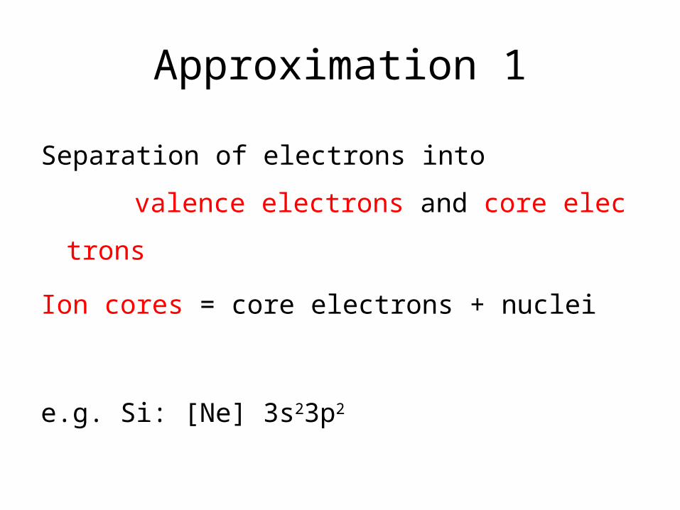
Separation of electrons into
valence electrons and core electrons
Ion cores = core electrons + nuclei
e.g. Si: [Ne] 3s23p2
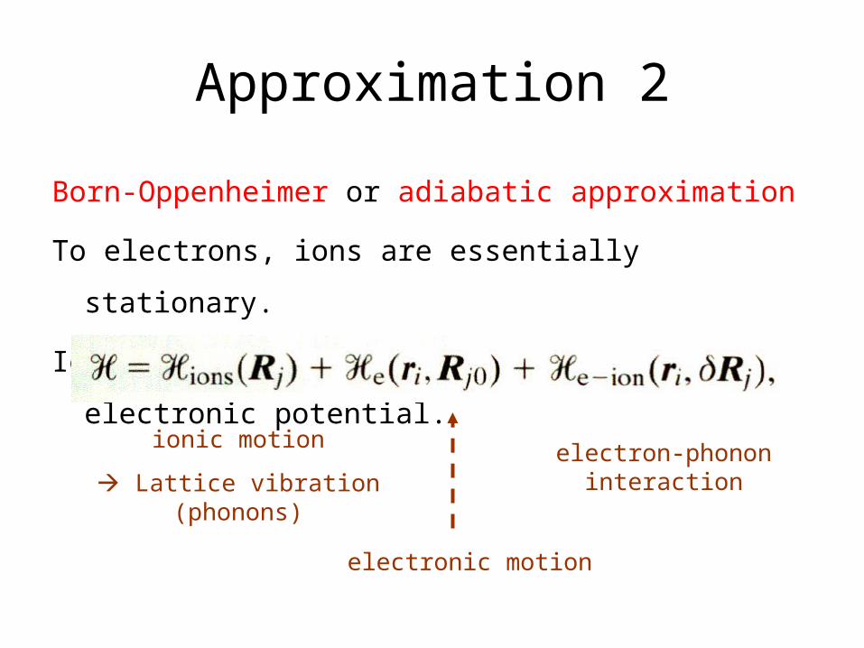
Approximation 2
Born-Oppenheimer or adiabatic approximation
To electrons, ions are essentially stationary.
Ions only see a time-averaged adiabatic electronic potential.
electron-phonon interaction
ionic motion
Lattice vibration (phonons)
electronic motion
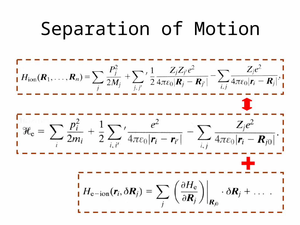
Separation of Motion
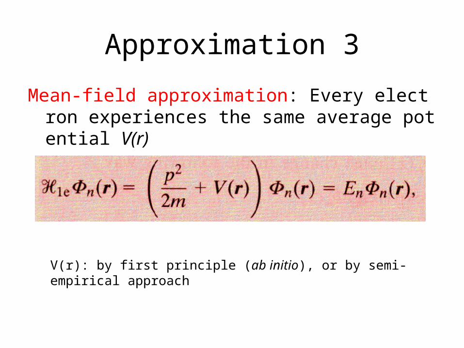
Approximation 3
Mean-field approximation: Every electron experiences the same average potential V(r)
V(r): by first principle (ab initio), or by semi-empirical approach
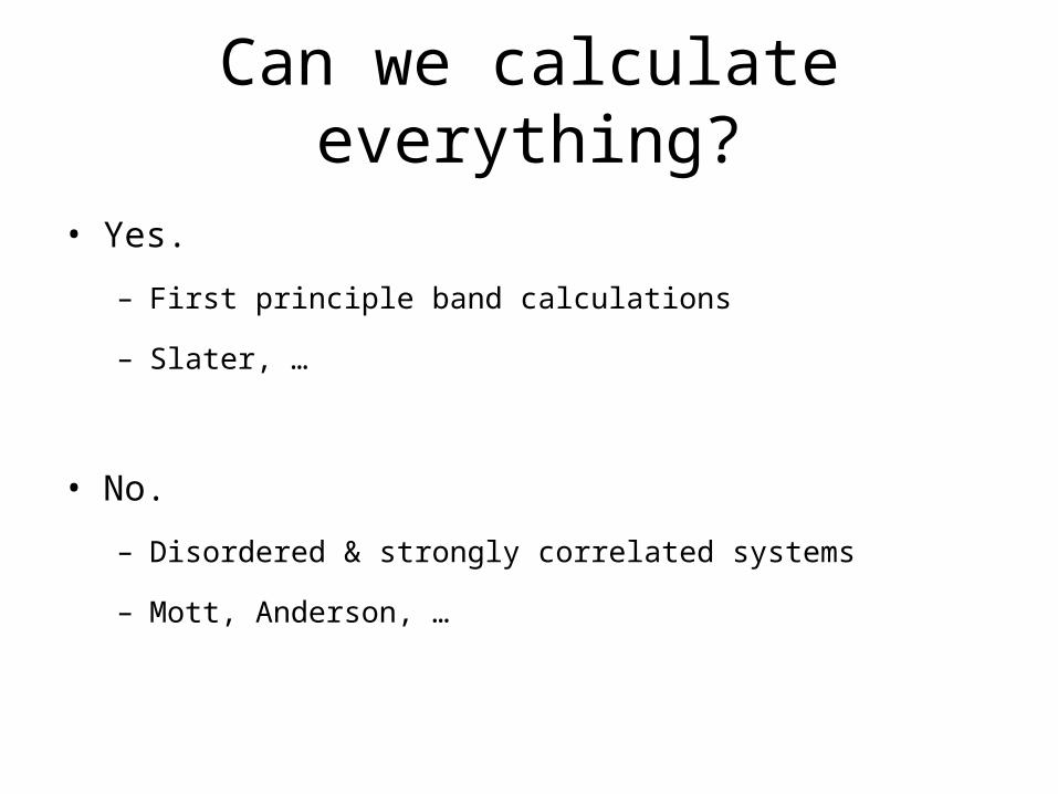
Can we calculate everything?
• Yes.
– First principle band calculations
– Slater, …
• No.
– Disordered & strongly correlated systems
– Mott, Anderson, …
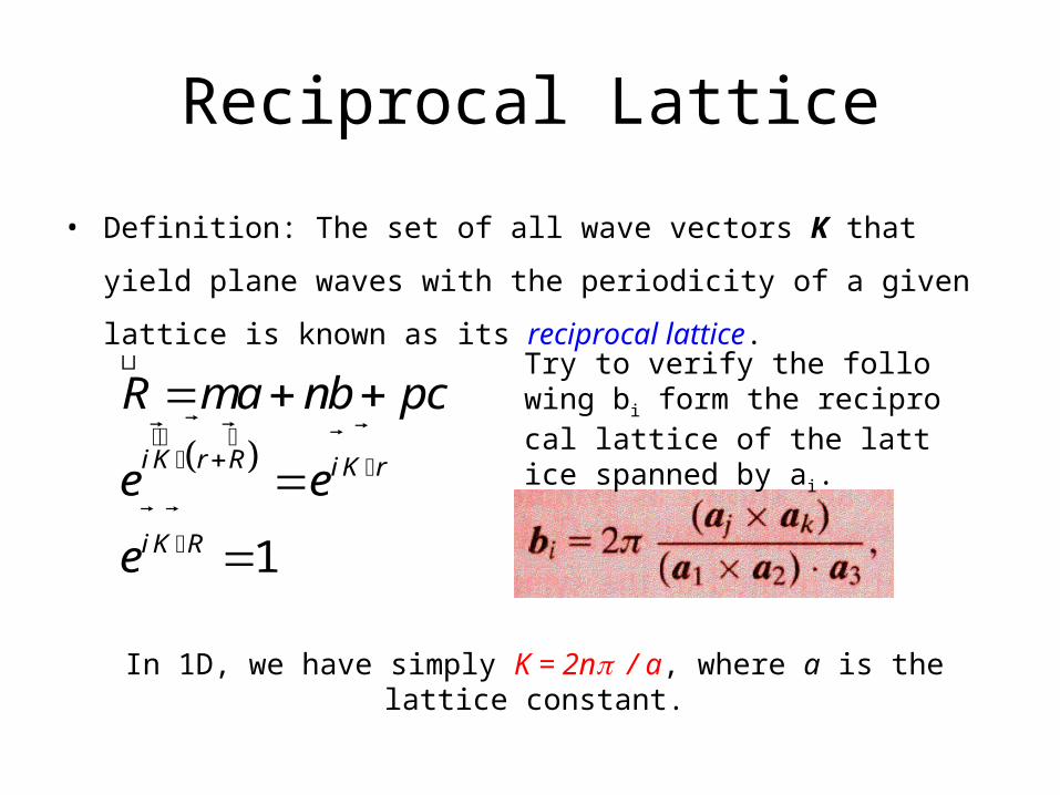
Reciprocal Lattice
• Definition: The set of all wave vectors K that yield plane waves with
the periodicity of a given lattice is known as its reciprocal lattice.
1
iK r R iK r
iK R
R ma nb pc
e e
e
������������������������������������������ ����������������������������
����������������������������
�������������������������������������������������������� Try to verify the following bi form the reciprocal lattice of the lattice spanned by ai.
In 1D, we have simply K = 2n/ a, where a is the lattice constant.
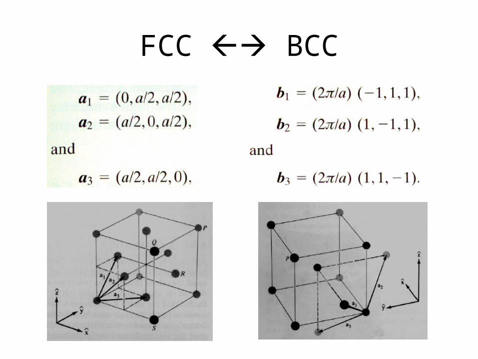
FCC BCC
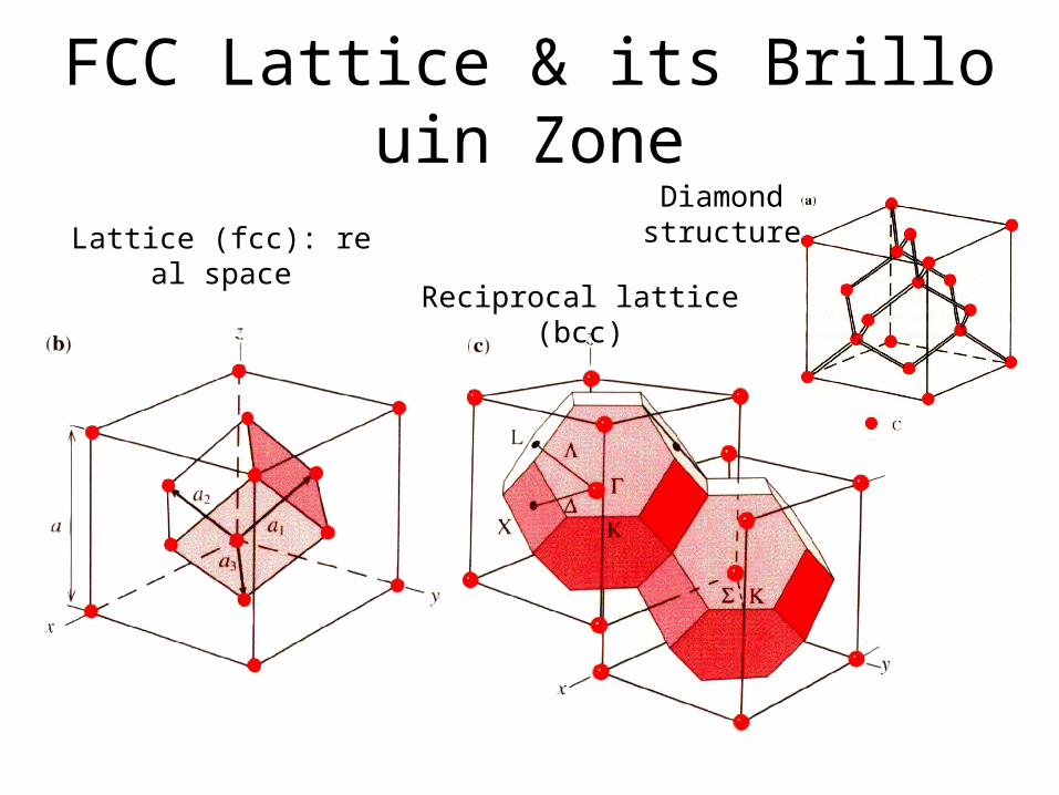
FCC Lattice & its Brillouin Zone
Lattice (fcc): real space
Reciprocal lattice (bcc)
Diamond structure
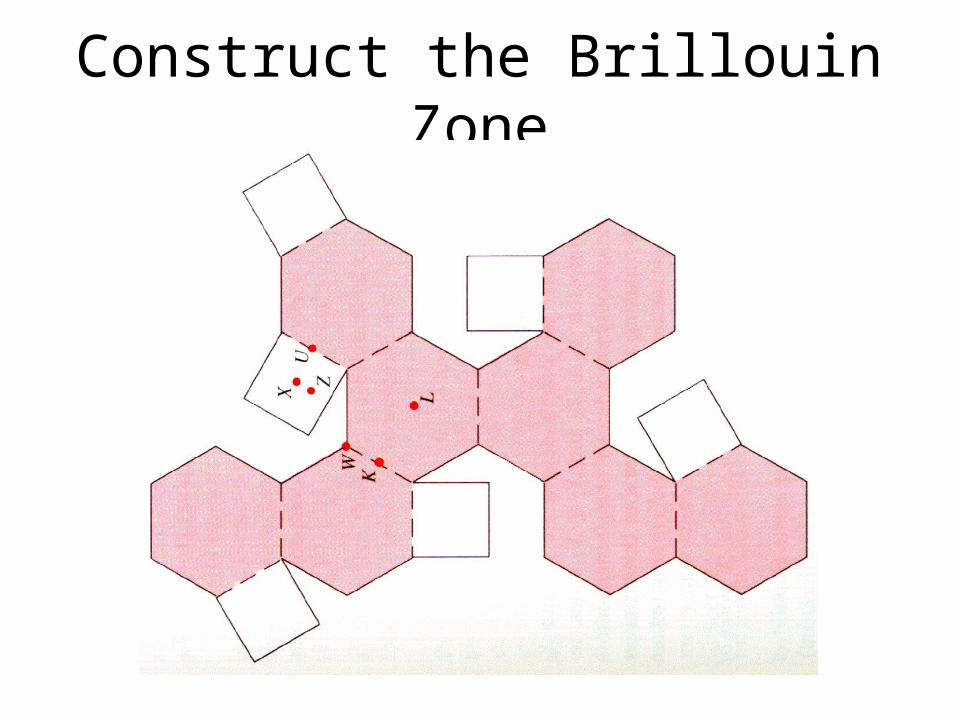
Construct the Brillouin Zone
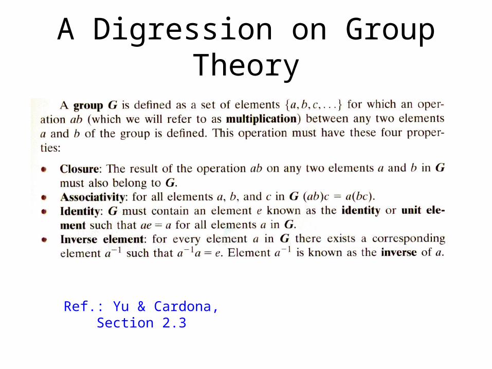
A Digression on Group Theory
Ref.: Yu & Cardona, Section 2.3
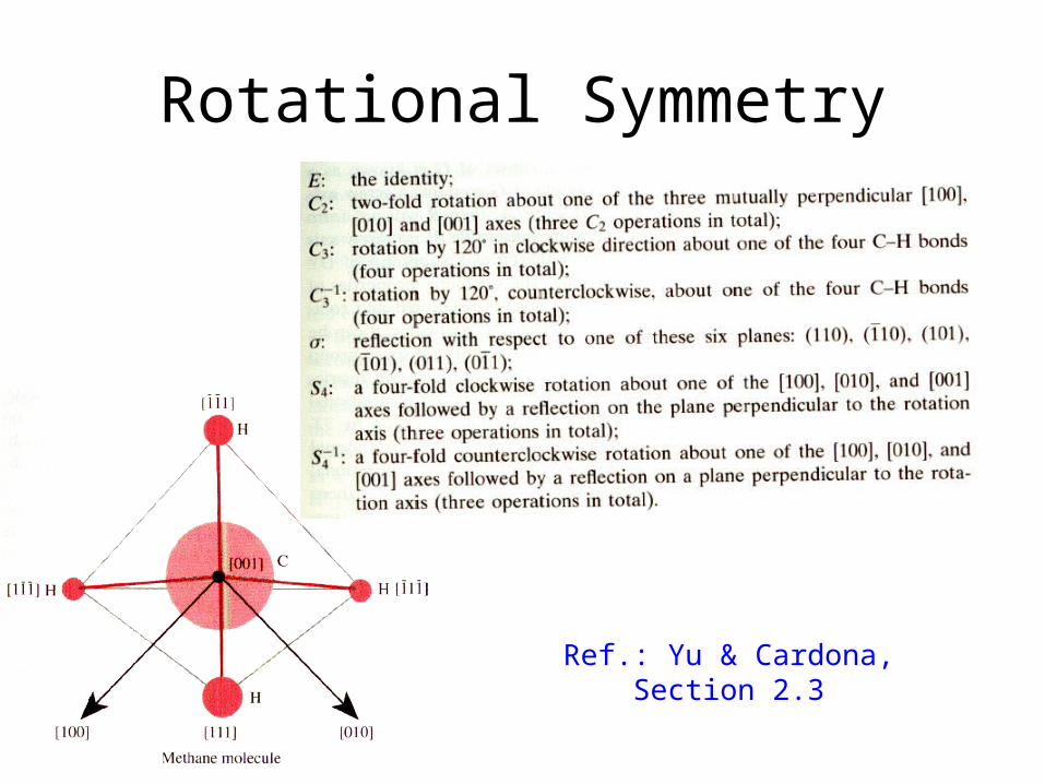
Rotational Symmetry
Ref.: Yu & Cardona, Section 2.3
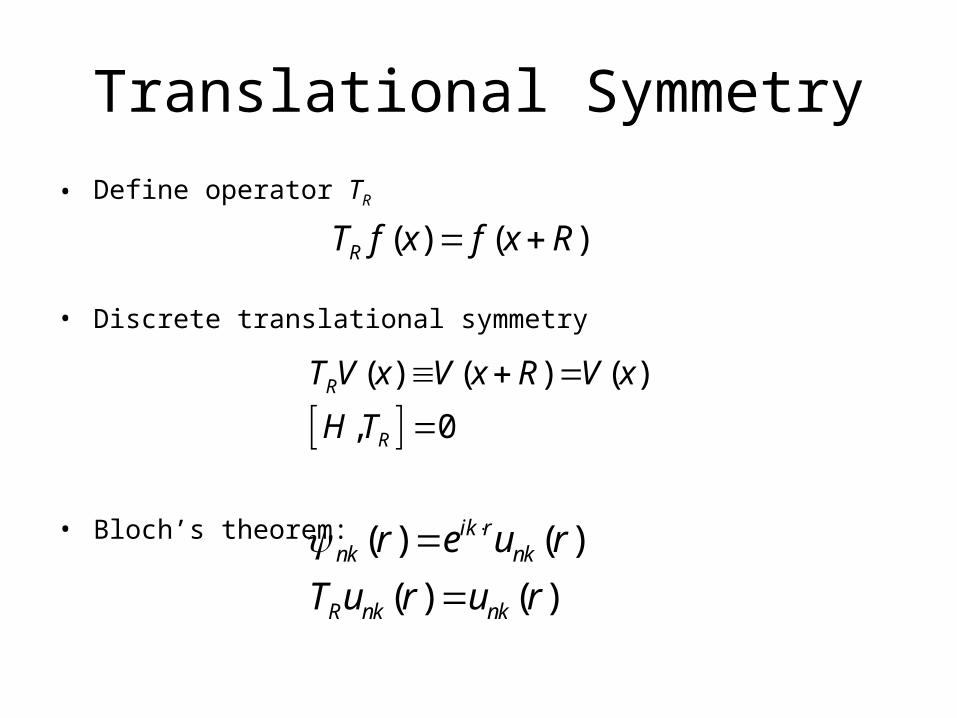
Translational Symmetry
• Define operator TR
• Discrete translational symmetry
• Bloch’s theorem:
( ) ( ) ( )
, 0R
R
T V x V x R V x
H T
( ) ( )RT f x f x R
( ) ( )
( ) ( )
ik rnk nk
R nk nk
r e u r
T u r u r
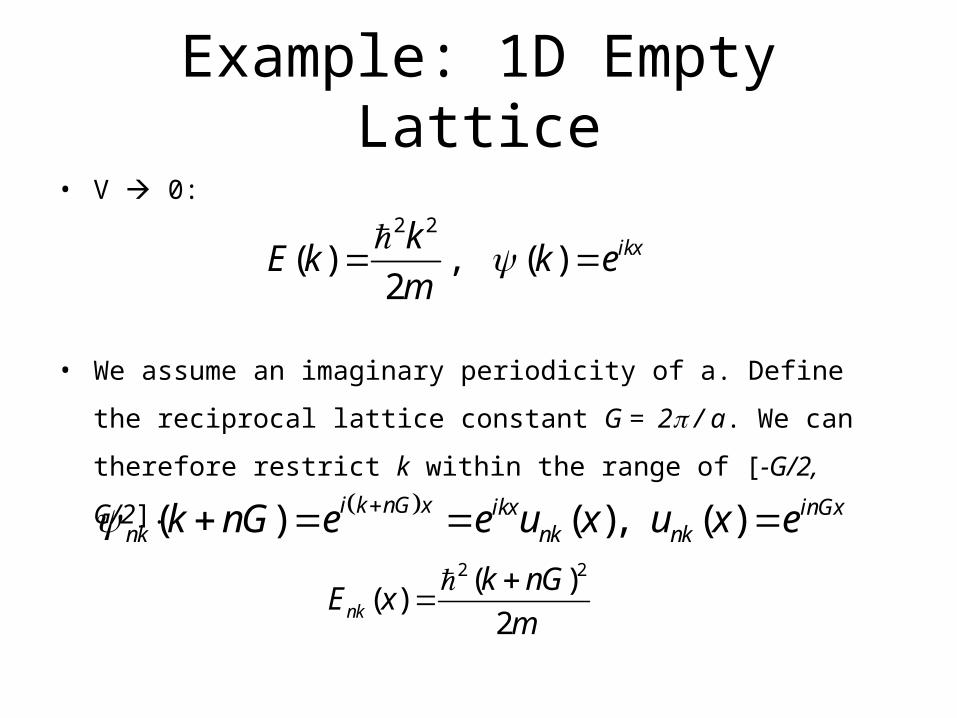
Example: 1D Empty Lattice
( ) ( ), ( )i k nG x ikx inGxnk nk nkk nG e e u x u x e
• V 0:
• We assume an imaginary periodicity of a. Define the reciprocal
lattice constant G = 2 / a. We can therefore restrict k within the
range of [-G/2, G/2].
2 2
( ) , ( )2
ikxkE k k e
m
2 2( )( )
2nk
k nGE x
m
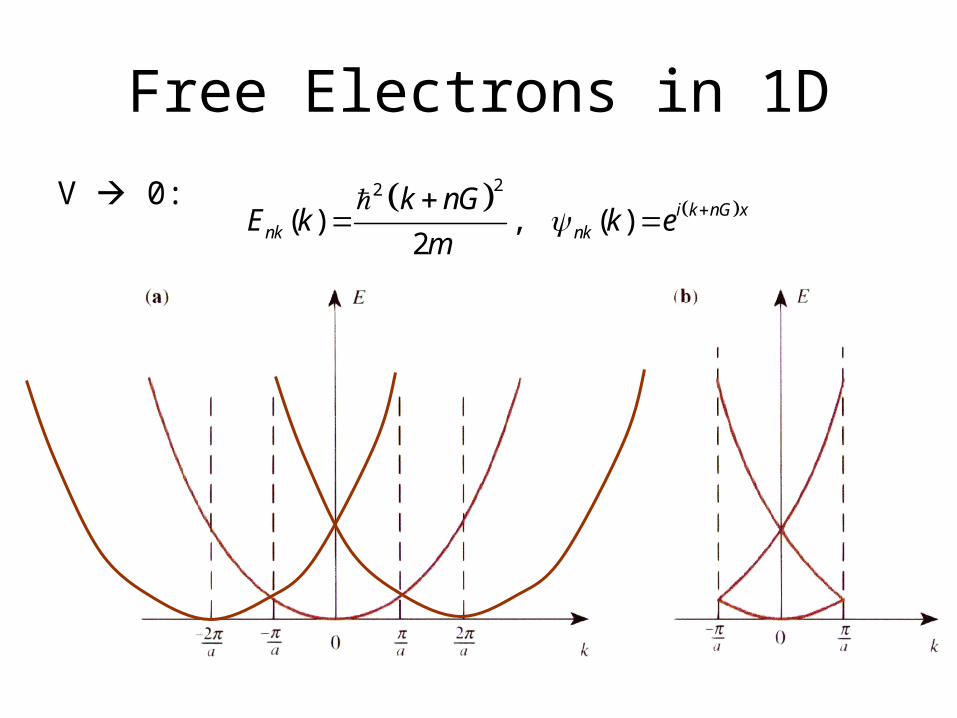
Free Electrons in 1D
V 0: 22
( ) , ( )2
i k nG xnk nk
k nGE k k e
m
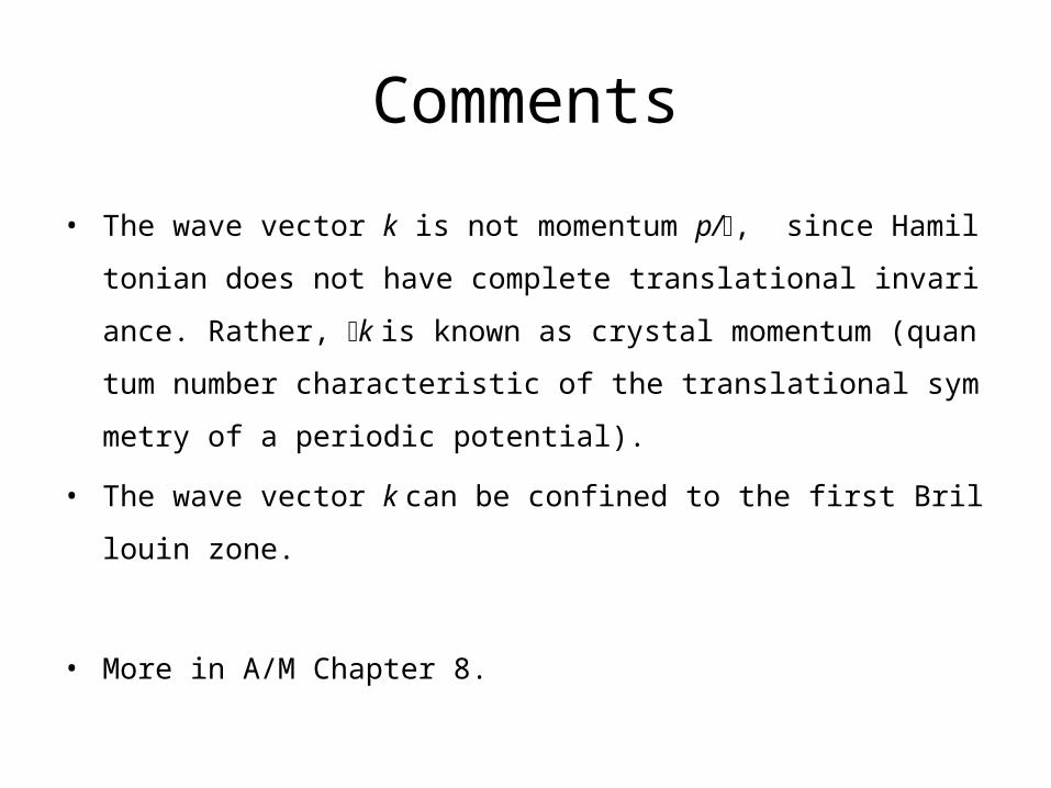
Comments
• The wave vector k is not momentum p/, since Hamiltonian does no
t have complete translational invariance. Rather, k is known as crys
tal momentum (quantum number characteristic of the translational s
ymmetry of a periodic potential).
• The wave vector k can be confined to the first Brillouin zone.
• More in A/M Chapter 8.
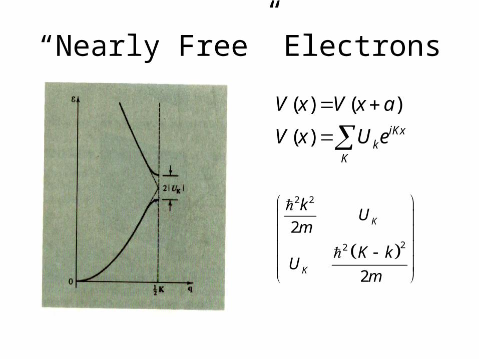
“Nearly Free” Electrons
( ) ( )
( ) iKxk
K
V x V x a
V x U e
2 2
22
2
2
K
K
kU
m
K kU
m
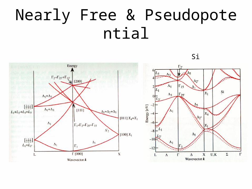
Nearly Free & Pseudopotential
Si
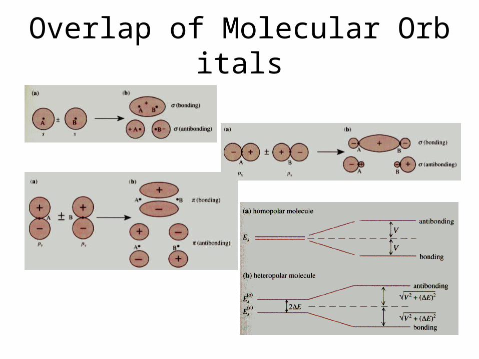
Overlap of Molecular Orbitals
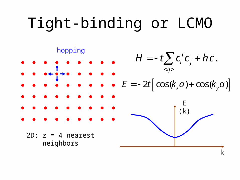
Tight-binding or LCMO
hopping. .i j
ij
H t c c h c
2 cos( ) cos( )x yE t k a k a
E(k)
k
2D: z = 4 nearest neighbors
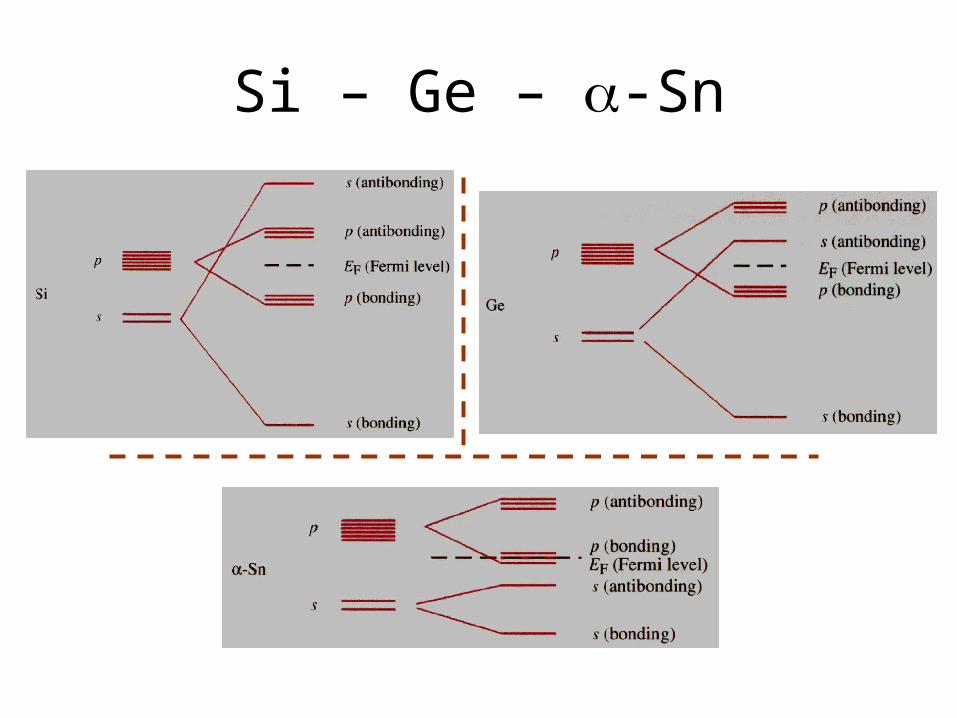
Si – Ge – -Sn
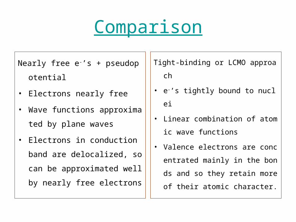
Comparison
Nearly free e-’s + pseudopotential
• Electrons nearly free
• Wave functions approximated
by plane waves
• Electrons in conduction band a
re delocalized, so can be appr
oximated well by nearly free el
ectrons
Tight-binding or LCMO approach
• e-’s tightly bound to nuclei
• Linear combination of atomic w
ave functions
• Valence electrons are concentr
ated mainly in the bonds and s
o they retain more of their ato
mic character.
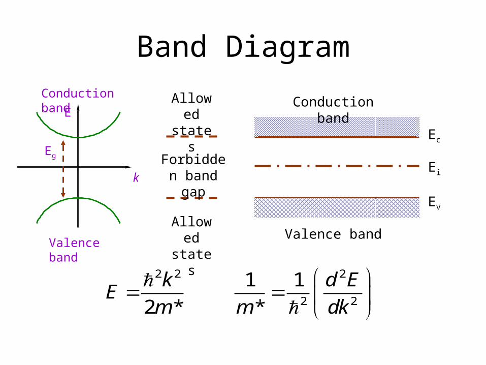
Band DiagramConduction band
Valence band
E
k
Conduction band
Valence band
Allowed states
Allowed states
Forbidden band gap
Ec
Ei
Ev
2 2 2
2 2
1 1
2 * *
k d EE
m m dk
Eg
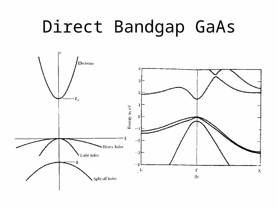
Direct Bandgap GaAs
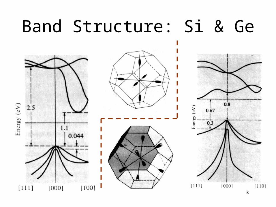
Band Structure: Si & Ge
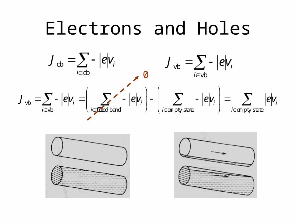
Electrons and Holes
vbvb filled band empty state empty state
i i i ii i i i
J ev ev ev ev
vbvb
ii
J ev
cbcb
ii
J ev
0
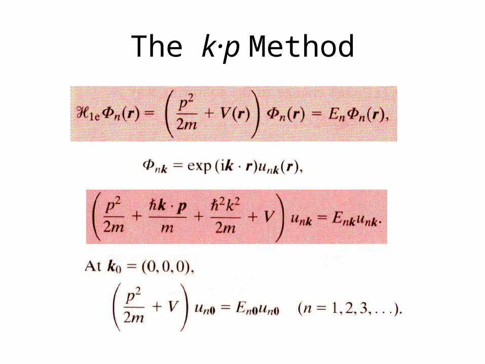
The k·p Method
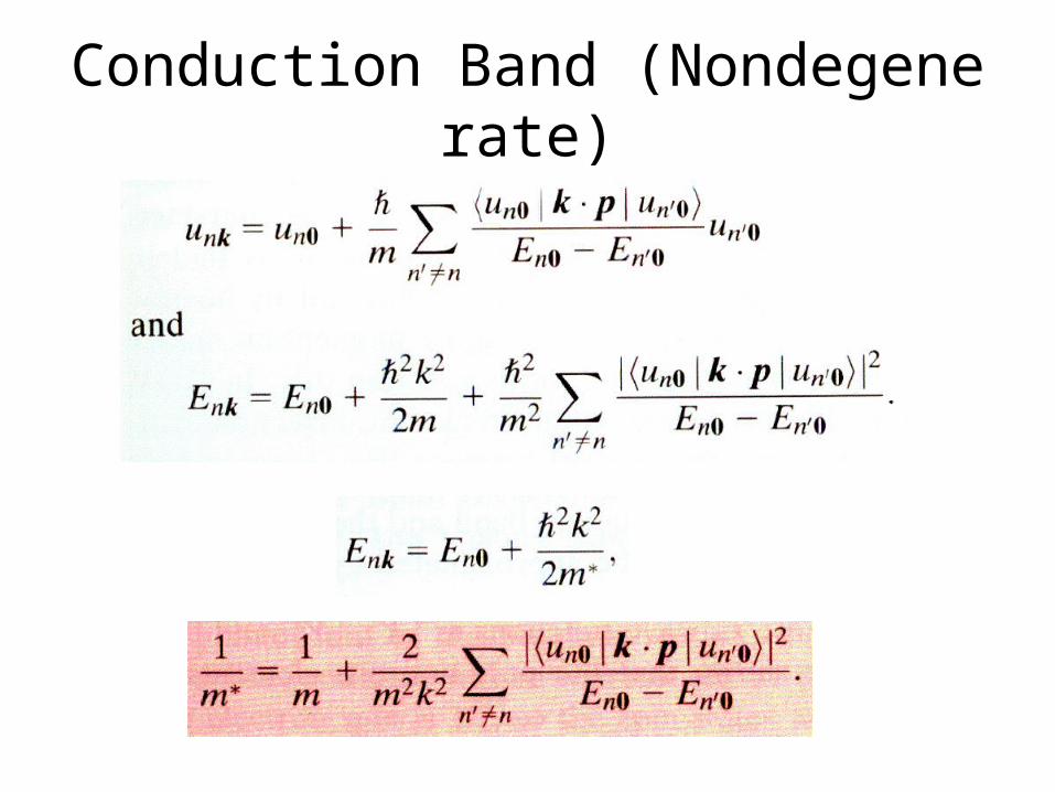
Conduction Band (Nondegenerate)
Comment on k·p Method
• Band structure over the entire BZ can be extrapolated by the zone c
enter energy gaps and optical matrix elements.
• One can btain analytical expression for band dispersion and effectiv
e mass around high-symmetry points.
• Nondegenerate perturbation is applicable to the conduction band mi
nimum in direct-bandgap semiconductors (zinc-blende, wurtzite); de
generate perturbation to top valence band (diamond, zinc-blende, w
urtzite). Ref.: Yu & Cardona, Section 2.6
• The trend of m* can be explained.
Chapter 1. Fundamentals
1.1 Bonds and bands
1.2 Impurities and defects
– Classification of defects
– Point defects
– Shallow (hydrogenic) impurities
1.3 Statistical distribution of charge carriers
1.4 Charge transport
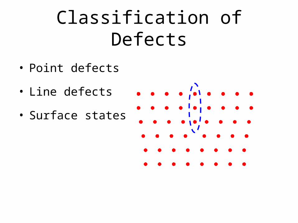
Classification of Defects
• Point defects
• Line defects
• Surface states
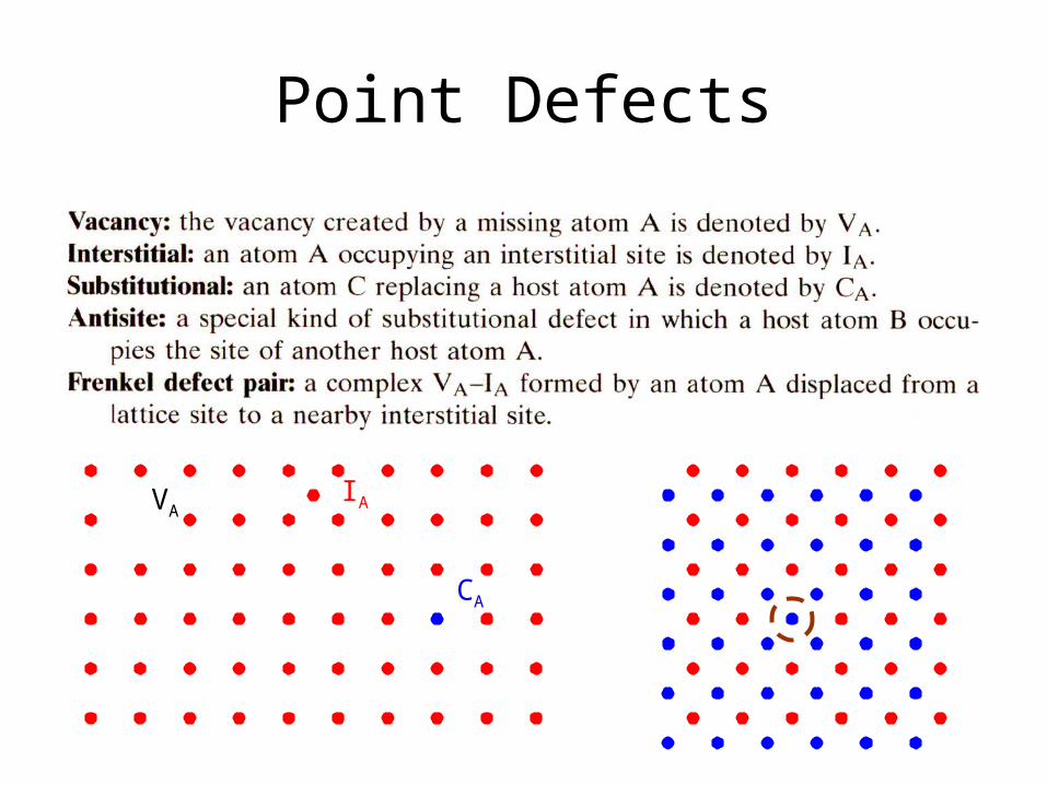
Point Defects
VAIA
CA
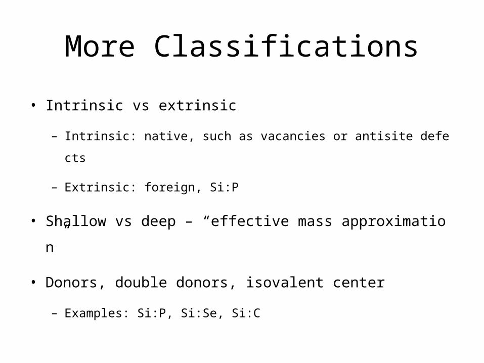
More Classifications
• Intrinsic vs extrinsic
– Intrinsic: native, such as vacancies or antisite defects
– Extrinsic: foreign, Si:P
• Shallow vs deep – “effective mass approximation”
• Donors, double donors, isovalent center
– Examples: Si:P, Si:Se, Si:C
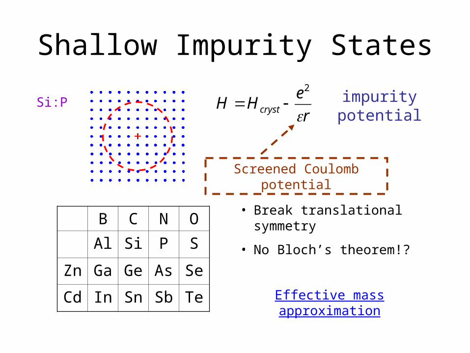
Shallow Impurity States
r
eHH cryst
2
impurity potential
B C N O
Al Si P S
Zn Ga Ge As Se
Cd In Sn Sb Te
Si:P
Effective mass approximation
• Break translational symmetry
• No Bloch’s theorem!?
Screened Coulomb potential
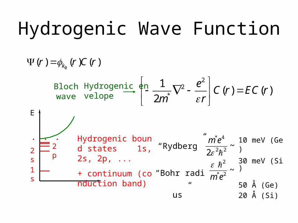
Hydrogenic Wave Function
1s
E
2s2p
...
0( ) ( ) ( )kr r C r
Bloch wave
Hydrogenic envelope
22
*
1( ) ( )
2
eC r EC r
m r
Hydrogenic bound states 1s, 2s, 2p, ...
+ continuum (conduction band)
“Rydberg”
“Bohr radius”
~2 22
4*
em
~2*
2
em
10 meV (Ge)
30 meV (Si)
50 Å (Ge)
20 Å (Si)
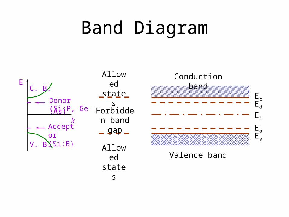
Band Diagram
Donor (Si:P, Ge:As)
C. B.
V. B.
Acceptor (Si:B)
E
k
Conduction band
Valence band
Allowed states
Allowed states
Forbidden band gap
EcEd
Ei
EaEv
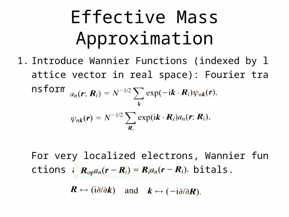
Effective Mass Approximation
1. Introduce Wannier Functions (indexed by lattice vector i
n real space): Fourier transforms of Bloch functions
For very localized electrons, Wannier functions are roug
hly atomic orbitals.
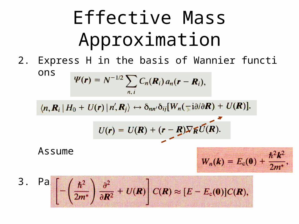
Effective Mass Approximation
2. Express H in the basis of Wannier functions
Assume
3. Parabolic, isotropic, nondegenerate
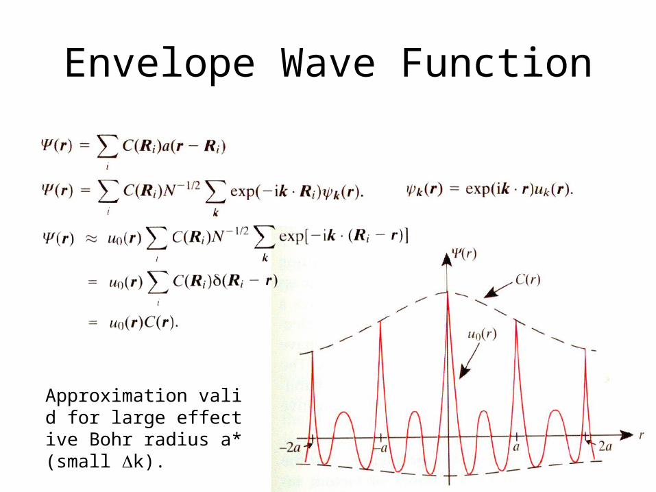
Envelope Wave Function
Approximation valid for large effective Bohr radius a*(small k).
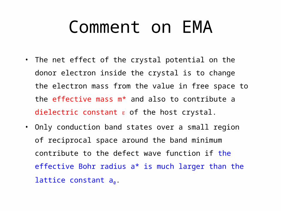
Comment on EMA
• The net effect of the crystal potential on the donor electron
inside the crystal is to change the electron mass from the
value in free space to the effective mass m* and also to
contribute a dielectric constant of the host crystal.
• Only conduction band states over a small region of reciprocal
space around the band minimum contribute to the defect
wave function if the effective Bohr radius a* is much larger
than the lattice constant a0.
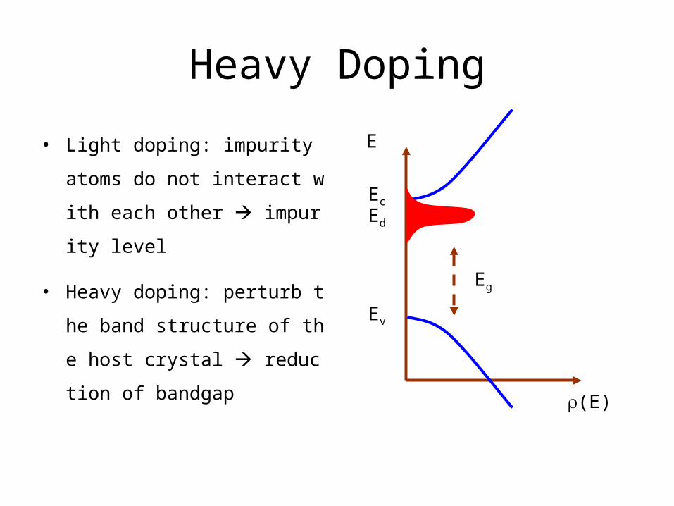
Heavy Doping
• Light doping: impurity atoms d
o not interact with each other
impurity level
• Heavy doping: perturb the ban
d structure of the host crystal
reduction of bandgap
E
(E)
Ec
Ed
Ev
Eg
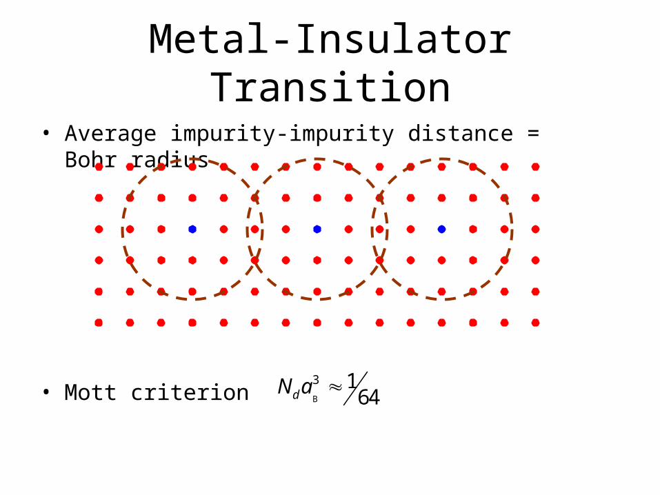
Metal-Insulator Transition
• Average impurity-impurity distance = Bohr radius
• Mott criterionB
3 164dN a
Chapter 1. Fundamentals
1.1 Bonds and bands
1.2 Impurities and defects
1.3 Statistical distribution of charge carriers
– Thermal equilibrium
– Mass-action law
– Fermi level
1.4 Charge transport
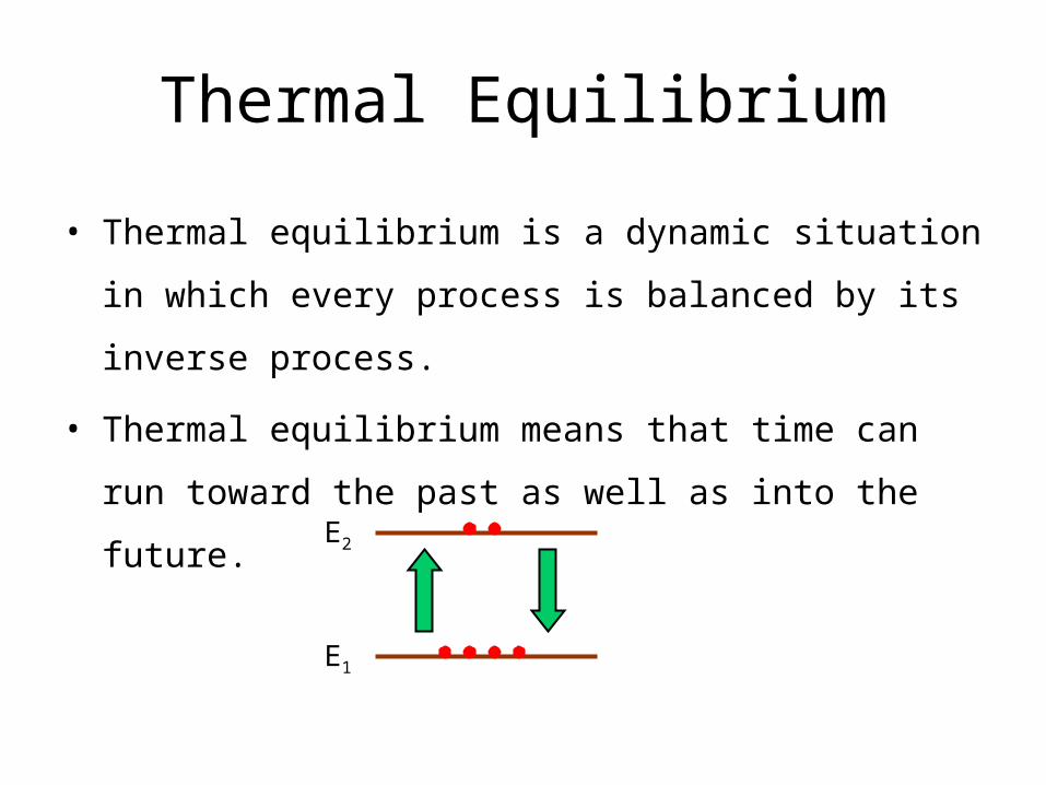
Thermal Equilibrium
• Thermal equilibrium is a dynamic situation in which every
process is balanced by its inverse process.
• Thermal equilibrium means that time can run toward the
past as well as into the future.
E1
E2
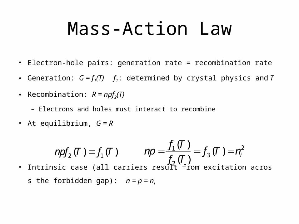
Mass-Action Law
• Electron-hole pairs: generation rate = recombination rate
• Generation: G = f1(T) f1: determined by crystal physics and T
• Recombination: R = npf2(T)
– Electrons and holes must interact to recombine
• At equilibrium, G = R
• Intrinsic case (all carriers result from excitation across the forbidde
n gap): n = p = ni
2 1( ) ( )npf T f T 213
2
( )( )
( ) i
f Tnp f T n
f T
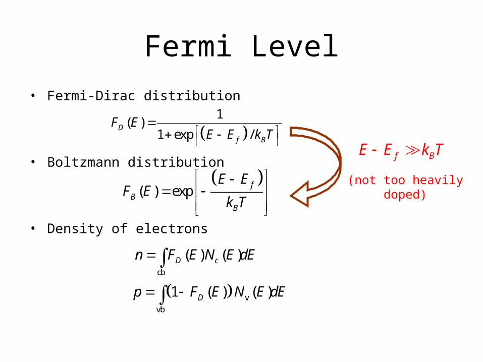
Fermi Level
• Fermi-Dirac distribution
• Boltzmann distribution
• Density of electrons
1
( )1 exp /
D
f B
F EE E k T
( ) exp
f
BB
E EF E
k T
f BE E k T
(not too heavily doped)
cb
( ) ( )D cn F E N E dE v
vb
1 ( ) ( )Dp F E N E dE
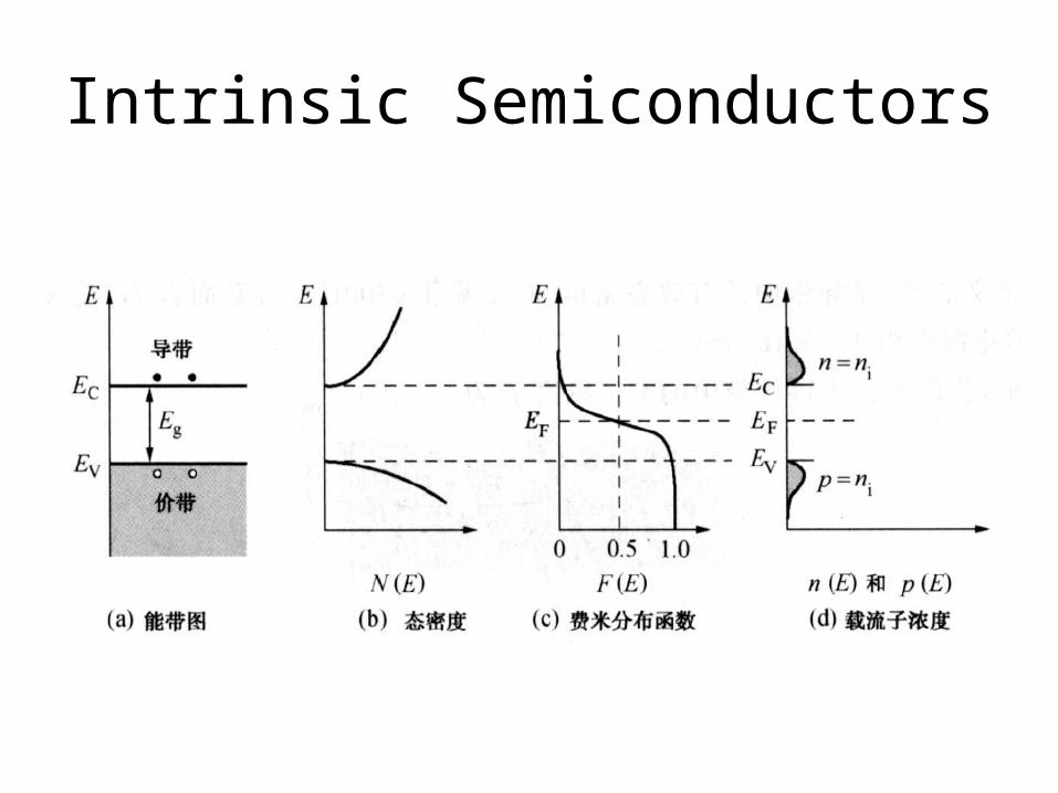
Intrinsic Semiconductors
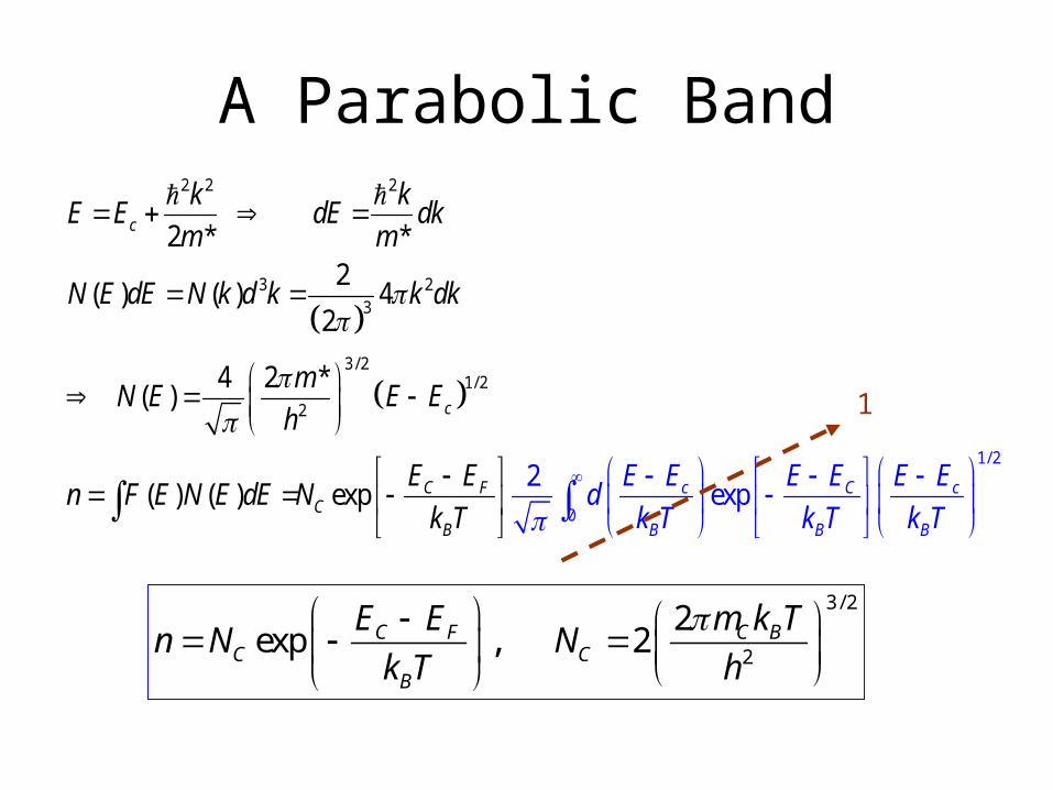
A Parabolic Band
2 2 2
3 23
3/ 22
1/ 2
1
2
0
/
2ex
2 * *2
( ) ( ) 42
4 2 *( )
( ) ( ) ex pp c C c
B
c
c
B
C FC
B B
k kE E dE dk
m m
N E dE N k d k k dk
mN E E E
h
E En F E
E E E E E Ed
k T kN E dE N
Tk kT T
1
3/ 2
2
2exp , 2C F C B
C CB
E E m k Tn N N
k T h
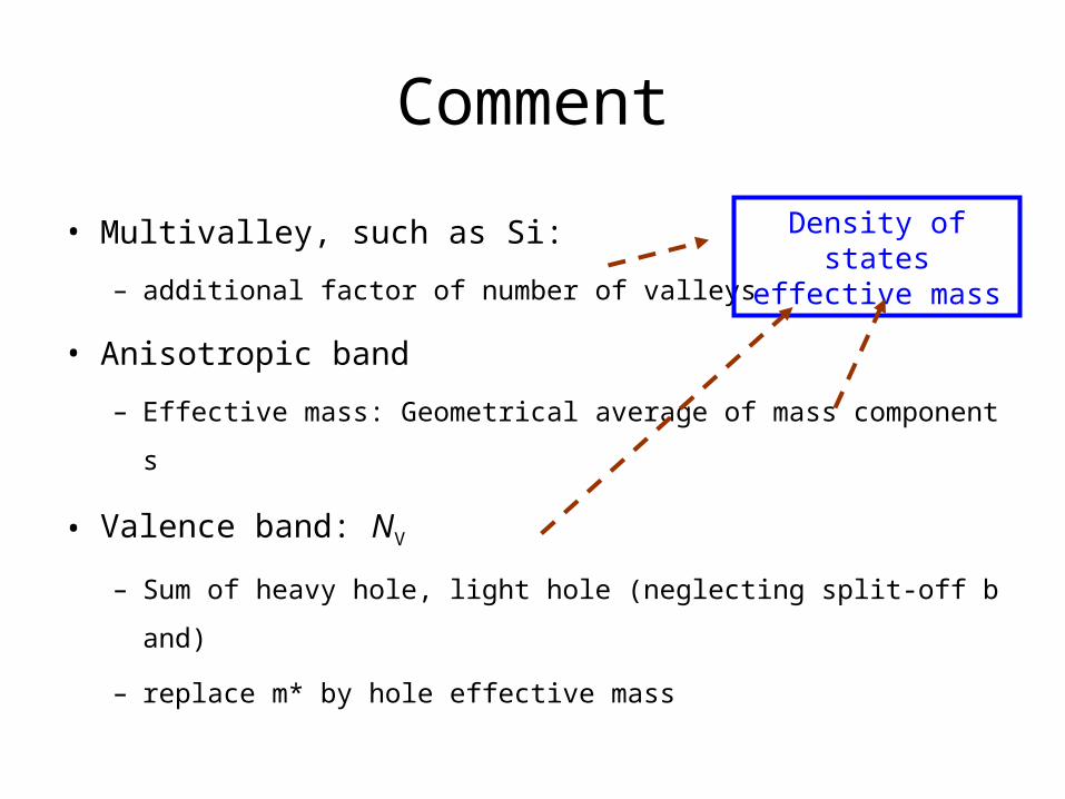
Comment
• Multivalley, such as Si:
– additional factor of number of valleys
• Anisotropic band
– Effective mass: Geometrical average of mass components
• Valence band: NV
– Sum of heavy hole, light hole (neglecting split-off band)
– replace m* by hole effective mass
Density of states effective mass
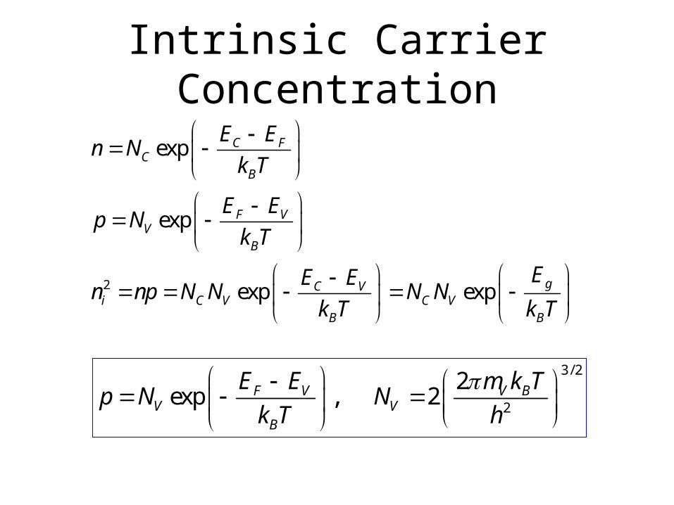
Intrinsic Carrier Concentration
2
exp
exp
exp exp
C FC
B
F VV
B
gC Vi C V C V
B B
E En N
k T
E Ep N
k T
EE En np N N N N
k T k T
3/ 2
2
2exp , 2F V V B
V VB
E E m k Tp N N
k T h
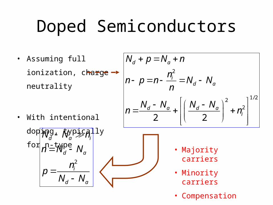
Doped Semiconductors
• Assuming full ionization,
charge neutrality
• With intentional doping,
typically for n-type
2
1/ 222
2 2
d a
id a
d a d ai
N p N n
nn p n N N
n
N N N Nn n
2
d a i
d a
i
d a
N N n
n N N
np
N N
• Majority carriers
• Minority carriers
• Compensation
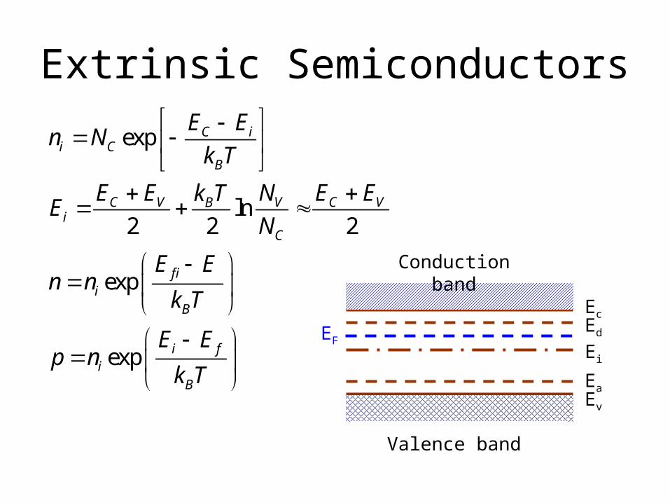
Extrinsic Semiconductors
exp
ln2 2 2
exp
exp
C ii C
B
C V V C VBi
C
f ii
B
i fi
B
E En N
k T
E E N E Ek TE
N
E En n
k T
E Ep n
k T
Conduction band
Valence band
EcEd
Ei
EaEv
EF
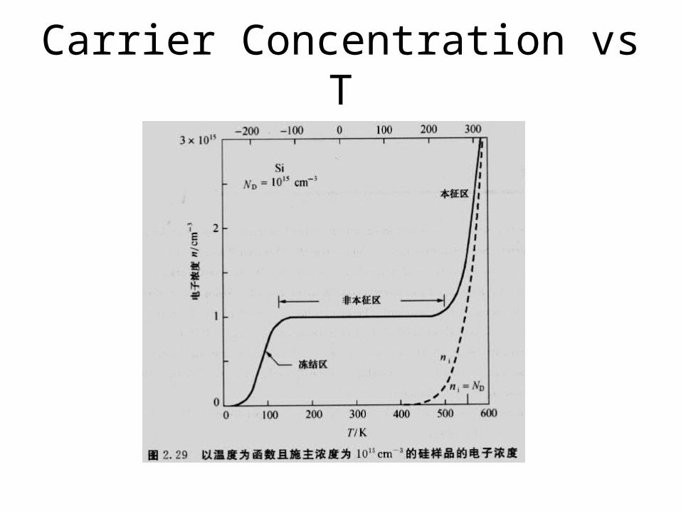
Carrier Concentration vs T
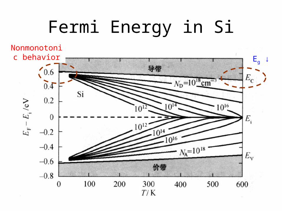
Fermi Energy in Si
Eg ↓
Nonmonotonic behavior
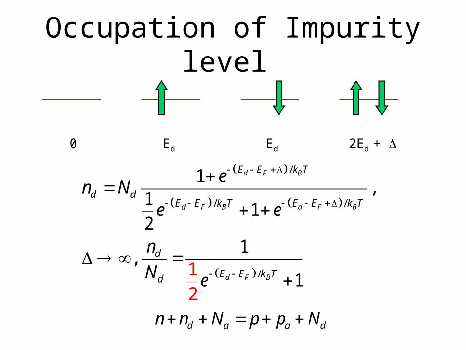
Occupation of Impurity level
/
/ /
/
1,
1
11
2
2
1,
1
d F B
d F B d F B
d F B
E E k T
d dE E k T E E k T
d
E E k Td
en N
e e
n
N e
0 Ed Ed 2Ed +
d a a dn n N p p N
Chapter 1. Fundamentals
1.1 Bonds and bands
1.2 Impurities and defects
1.3 Statistical distribution of charge carriers
1.4 Charge transport
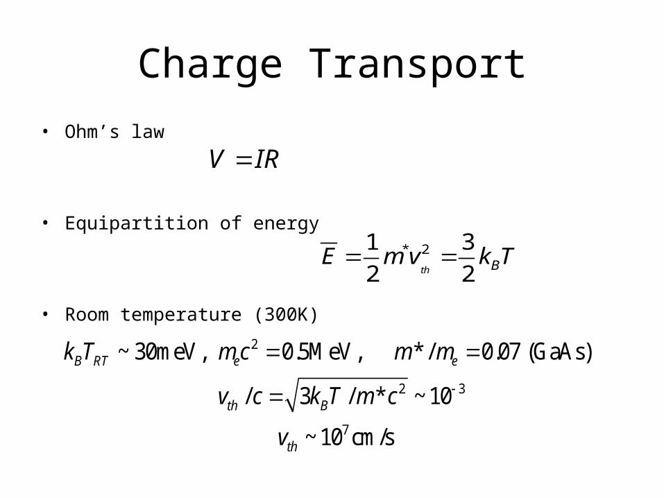
Charge Transport
• Ohm’s law
• Equipartition of energy
• Room temperature (300K)
V IR
* 21 3
2 2th BE m v k T
2
2 3
7
~ 30meV, 0.5MeV, * / 0.07 (GaAs)
/ 3 / * ~ 10
~ 10 cm/s
B RT e e
th B
th
k T m c m m
v c k T m c
v
The complete notes for Chapter 1 are expected to be available after
Sept. 20, 2006.