
Femtosecond Laser-Induced Ripple Structures in Semiconductor
5
JLMN-Journal of Laser Micro/Nanoengineering Vol. 2, No. 2, 2007 Femtosecond Laser-Induced Ripple Structures in Semiconductor Materials Takuro Tomita, Keita Kinoshita, Toshiaki Murai, Yasuhiro Fukumori, Shigeki Matsuo, and Shuichi Hashimoto Department of Ecosystem Engineering, The University of Tokushima, 2-1 Minamijosanjima Tokushima 770-8506, Japan E-mail: [email protected] Femtosecond laser-induced ripple structures were fabricated on semiconductor materials such as silicon and silicon carbide. While a coarse ripple was observed on both materials under the proper irradiation conditions, a fine ripple was observed only on the silicon carbide. The cross-sectional profile of ripple structure was examined by scanning electron microscopy with sliced or tilted sam- ples. Based on the experimental observations, the formation mechanism of the ripple structure was discussed. Keywords: ripple, femtosecond laser, silicon, silicon carbide, threshold 1. Introduction Laser-induced ripples which have a variety of potential applications have been extensively studied in recent years. The ripples structure can be used for reducing the friction between materials and for fabricating nanogratings [1]. Ripple structures were first reported in 1965 by Birn- baum [2], and it was experimentally shown that the mean spacing of the ripple is approximately the same as the wavelength of normally incident laser beam. The formation of so-called “coarse ripples”, which has the period nearly the same as that of the normally incident laser beam, was explained by the interference between the incident laser beam and the surface scattered wave [3-7]. However, the ripples whose mean spacing is several times smaller than the laser wavelength are reported very recently [8, 9]. These ripples are called “fine ripple” and cannot be ex- plained by the classical interference model. Thus, the for- mation mechanism of ripple is the subject of a keen discus- sion [10-13]. This paper reports the irradiation condition dependence of ripple structures on high quality silicon and 4H-SiC sub- strates. We also report the cross-sectional profile of the ripple structure to discuss the possible formation mecha- nisms of the laser-induced ripples. 2. Experiment A Ti: Sapphire regenerative amplifier based on a chirped pulse amplification (CPA) system operating at 800 nm (Spectra-Physics, Spitfire) with the typical repetition rate of 1 kHz was used as a light source. The laser beam was fo- cused onto the sample by a plano-convex lens (f=100 mm), and the fluence of laser beam was attenuated by a variable neutral density filter. The laser pulse energy was monitored by a energymeter (OPHIR, LaserStar with PD10 / PE10). A polarization beam splitter was used to keep the polarization of laser beam horizontally. Prior to laser irradiation, the sample surface was cleaned with methanol and rinsed with distilled water. The samples used in this experiment were a single crystal silicon with (100) face (Mitsubishi Materials corp., impurities: Boron, resistivity: 6.0 (Ωcm)) and a n- type single crystal 4H-SiC (Sterling Semiconductor Inc. resistivity: 0.05 (Ωcm)). The laser-irradiated surface was scrutinized by the scanning electron microscopy (SEM). 3. Results 3.1 Coarse ripple structures on silicon The SEM image of ripple structures on the silicon sur- face was shown in Fig. 1. The pulse energy of incident la- ser beam was 0.7μJ/pulse and 200 pulses were irradiated on the same spot with the pulse interval of 5 ms. Under this irradiation condition, a ripple structure was observed in a whole region of an ablated spot [14, 15]. Although we ex- amined the ripple formation for wide range of fluences and total number of pulses, we found only one type of ripple structure, i.e. so called a coarse ripple. This observation is in agreement with the previous reports [16, 17]. Since the band gap energy of silicon and the photon energy of inci- dent laser beam is 1.11 eV and 1.55 eV, respectively [18], the photon energy of incident laser beam exceeds the band gap of silicon. It was experimentally observed that the only the coarse ripple was found on the excitation above the band gap [19]. It is widely accepted that the coarse ripple has the pe- riod which is approximately similar to the wavelength of E Fig. 1 SEM image of ripple structure on silicon. The pulse energy of incident laser beam was 0.7 μJ/pulse. 200 pulses were irradiated with a pulse interval of 5ms. 141
Transcript of Femtosecond Laser-Induced Ripple Structures in Semiconductor

JLMN-Journal of Laser Micro/Nanoengineering Vol. 2, No. 2, 2007
Femtosecond Laser-Induced Ripple Structures in Semiconductor Materials
Takuro Tomita, Keita Kinoshita, Toshiaki Murai, Yasuhiro Fukumori, Shigeki Matsuo, and Shuichi Hashimoto
Department of Ecosystem Engineering, The University of Tokushima, 2-1 Minamijosanjima Tokushima 770-8506, Japan
E-mail: [email protected]
Femtosecond laser-induced ripple structures were fabricated on semiconductor materials such as silicon and silicon carbide. While a coarse ripple was observed on both materials under the proper irradiation conditions, a fine ripple was observed only on the silicon carbide. The cross-sectional profile of ripple structure was examined by scanning electron microscopy with sliced or tilted sam-ples. Based on the experimental observations, the formation mechanism of the ripple structure was discussed.
Keywords: ripple, femtosecond laser, silicon, silicon carbide, threshold
1. Introduction Laser-induced ripples which have a variety of potential
applications have been extensively studied in recent years. The ripples structure can be used for reducing the friction between materials and for fabricating nanogratings [1].
Ripple structures were first reported in 1965 by Birn-baum [2], and it was experimentally shown that the mean spacing of the ripple is approximately the same as the wavelength of normally incident laser beam. The formation of so-called “coarse ripples”, which has the period nearly the same as that of the normally incident laser beam, was explained by the interference between the incident laser beam and the surface scattered wave [3-7]. However, the ripples whose mean spacing is several times smaller than the laser wavelength are reported very recently [8, 9]. These ripples are called “fine ripple” and cannot be ex-plained by the classical interference model. Thus, the for-mation mechanism of ripple is the subject of a keen discus-sion [10-13].
This paper reports the irradiation condition dependence of ripple structures on high quality silicon and 4H-SiC sub-strates. We also report the cross-sectional profile of the ripple structure to discuss the possible formation mecha-nisms of the laser-induced ripples.
2. Experiment A Ti: Sapphire regenerative amplifier based on a chirped
pulse amplification (CPA) system operating at 800 nm (Spectra-Physics, Spitfire) with the typical repetition rate of 1 kHz was used as a light source. The laser beam was fo-cused onto the sample by a plano-convex lens (f=100 mm), and the fluence of laser beam was attenuated by a variable neutral density filter. The laser pulse energy was monitored by a energymeter (OPHIR, LaserStar with PD10 / PE10). A polarization beam splitter was used to keep the polarization of laser beam horizontally. Prior to laser irradiation, the sample surface was cleaned with methanol and rinsed with distilled water. The samples used in this experiment were a single crystal silicon with (100) face (Mitsubishi Materials corp., impurities: Boron, resistivity: 6.0 (Ωcm)) and a n-
type single crystal 4H-SiC (Sterling Semiconductor Inc. resistivity: 0.05 (Ωcm)). The laser-irradiated surface was scrutinized by the scanning electron microscopy (SEM).
3. Results
3.1 Coarse ripple structures on silicon The SEM image of ripple structures on the silicon sur-
face was shown in Fig. 1. The pulse energy of incident la-ser beam was 0.7μJ/pulse and 200 pulses were irradiated on the same spot with the pulse interval of 5 ms. Under this irradiation condition, a ripple structure was observed in a whole region of an ablated spot [14, 15]. Although we ex-amined the ripple formation for wide range of fluences and total number of pulses, we found only one type of ripple structure, i.e. so called a coarse ripple. This observation is in agreement with the previous reports [16, 17]. Since the band gap energy of silicon and the photon energy of inci-dent laser beam is 1.11 eV and 1.55 eV, respectively [18], the photon energy of incident laser beam exceeds the band gap of silicon. It was experimentally observed that the only the coarse ripple was found on the excitation above the band gap [19].
It is widely accepted that the coarse ripple has the pe-riod which is approximately similar to the wavelength of
E
Fig. 1 SEM image of ripple structure on silicon. The pulse energy of incident laser beam was 0.7 μJ/pulse. 200 pulses were irradiated with a pulse interval of 5ms.
141

JLMN-Journal of Laser Micro/Nanoengineering Vol. 2, No. 2, 2007 incident laser beam [2-7]. However, to our knowledge, only few papers reported the detailed analysis and discussion of the deviation of the period of ripples from the wavelength of incident laser beam [13]. We applied the two-dimensional Fourier transform method (2D-FT) in order to precisely evaluate the period of ripples. The period of the ripple which is evaluated by 2D-FT was approximately 600 nm. This is slightly but distinctly smaller than the wave-length of the incident laser beam.
According to the classical interference model for ripple formation, the period of ripple can be given as follows [6]:
Fig. 3 SEM image of laser-induced periodic structures on 4H-SiC. The laser fluence at the center of a beam spot was 3.1 J/cm2. The inset shows a magnified image. Fine and coarse ripples are observed at the peripheral and central regions, respectively. The arrow represents the direction of the electric field of the laser beam.
×2E
10μm
θλsin1±
=Λ . (1)
Here, is the period of ripple, Λ λ is the wavelength of in-cident laser beam, and θ is the incident angle. Under the present experimental condition, the experimental parame-ters are given as follows;
(nm) 800=λ and (degree) 0=θ , thus, the calculated period of ripple was 800 nm. This value is not in good agreement with the experimentally observed period of ripple. This small deviation is often reported, and usually explained by the inclination of incident angle due to tilting of surface by a laser ablated crater [13]. However, the detailed analysis of the cross-sectional profiles of ripple is needed to clarify the effect of crater.
We thus observed the cross-sectional profile of ripple on the silicon surface.
3.2 Cross-sectional image of the ripple on Si To discuss the cross-sectional profile of ripple on sili-
con, the irradiated sample was cut perpendicularly across the center of ripple by a focused ion beam (FIB). Fig. 2 shows the SEM image of the crosssection. The SEM image was captured with the tilted angle of 10°. It is found that the surface of ripple is nearly flat and shows no sign of crater formation due to laser ablation under this irradiation condition. Thus, we conclude that the laser was irradiated perpendicularly ( 0=θ ) to the silicon surface within an experimental error.
If we assume that the observed period of ripple is ex-plained by the classical interference model i.e. eq. (1), the value of θ should be around 20°. But, this is not the case. Although, this is not enough for excluding the possibility of
classical interference model for explaining coarse ripple formation, it is worth noting whether the model can fully explain the formation of coarse ripple. In the Section 4, we will further discuss the formation of the coarse ripple.
3.3 Fine and coarse ripple structures on 4H-SiC The SEM image of ripple structures on the irradiation
of femtosecond laser pulse on 4H-SiC was shown in Fig. 3. In this figure, the direction of the electric field of incident laser beam was shown by a white arrow, and the magnified image was shown in the inset. On the whole area, we can find clear ripple structures which can be classified into two types. The ripple found on the central region is a coarse ripple which has a periodicity close to the wavelength of the incident laser beam, and the ripple on the peripheral region is a fine ripple whose periodicity is much smaller than that of the wavelength of the incident laser beam. Since the band gap energy of 4H-SiC and the photon en-ergy of incident laser beam is 3.27 eV and 1.55 eV, respec-tively [18], the photon energy of incident laser beam is lower than the band gap of 4H-SiC. It is experimentally revealed that both the coarse and fine ripples were found on the excitation below the band gap [19]. It is noteworthy that these ripple structures have the clear boundary the size of which depends on laser fluence. The periods of ripples evaluated from the two-dimensional Fourier transformation was about 500 nm and about 250 nm for coarse and fine ripple, respectively.
Fig. 2 Cross-sectional SEM image of ripple structures on silicon.
3.4 Pulse interval dependence of ripple formation For the industrial application of ripples especially for
high-speed processing, the information about pulse interval dependence of the ripple formation is necessary. To our knowledge, however, pulse interval dependence of ripple formation has not been investigated systematically. The threshold of each ripple was evaluated from the pulse flu-ence dependence of the diameter of each ripple [20, 21]. In this section, we will discuss the threshold of fine and coarse ripples.
An “incubation effect” is known to reduce the ablation (modification) threshold on multiple laser pulse irradiation. In general, the storage cycle of thermal stress–strain energy induced by a laser pulse has been regarded as the source of
142
JLMN-Journal of Laser Micro/Nanoengineering Vol. 2, No. 2, 2007
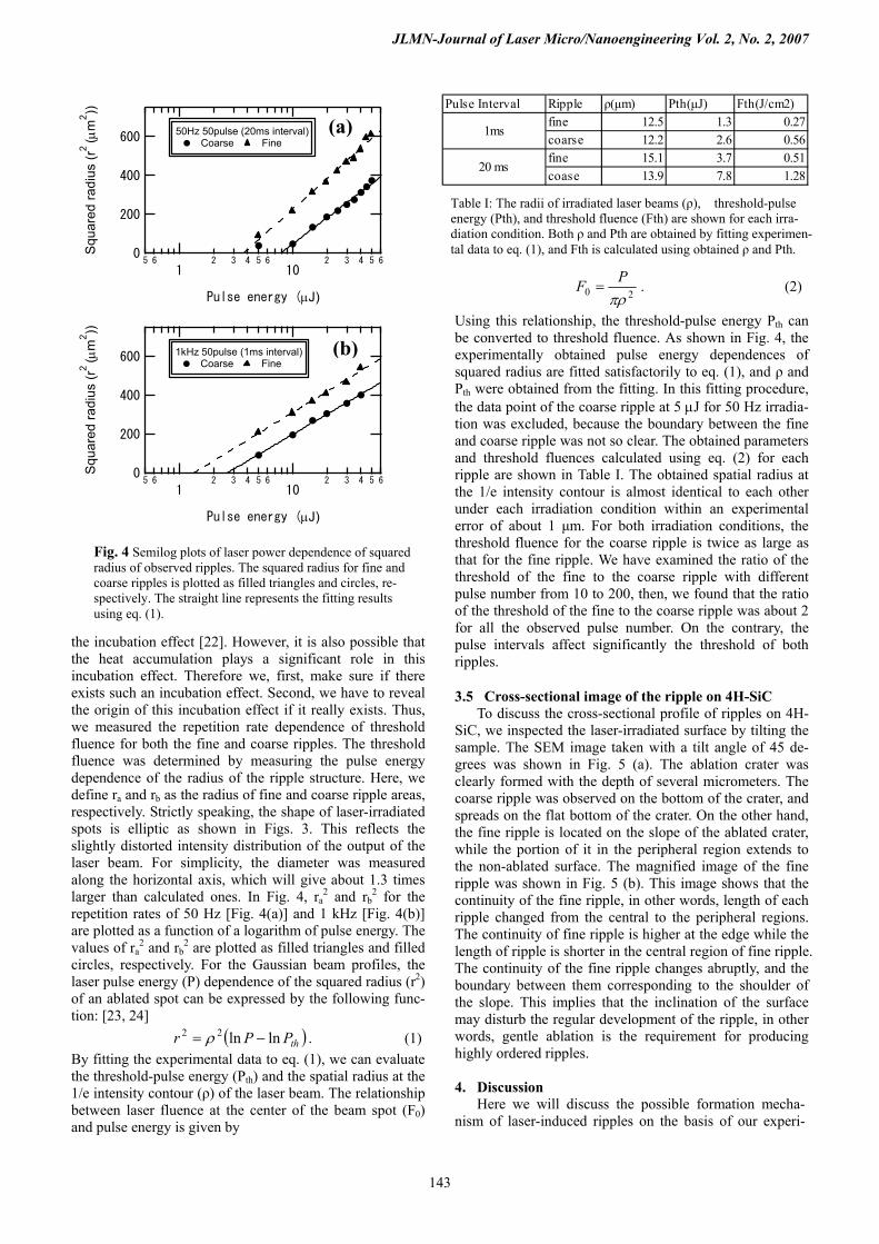
the incubation effect [22]. However, it is also possible that the heat accumulation plays a significant role in this incubation effect. Therefore we, first, make sure if there exists such an incubation effect. Second, we have to reveal the origin of this incubation effect if it really exists. Thus, we measured the repetition rate dependence of threshold fluence for both the fine and coarse ripples. The threshold fluence was determined by measuring the pulse energy dependence of the radius of the ripple structure. Here, we define ra and rb as the radius of fine and coarse ripple areas, respectively. Strictly speaking, the shape of laser-irradiated spots is elliptic as shown in Figs. 3. This reflects the slightly distorted intensity distribution of the output of the laser beam. For simplicity, the diameter was measured along the horizontal axis, which will give about 1.3 times larger than calculated ones. In Fig. 4, ra
2 and rb2 for the
repetition rates of 50 Hz [Fig. 4(a)] and 1 kHz [Fig. 4(b)] are plotted as a function of a logarithm of pulse energy. The values of ra
2 and rb2 are plotted as filled triangles and filled
circles, respectively. For the Gaussian beam profiles, the laser pulse energy (P) dependence of the squared radius (r2) of an ablated spot can be expressed by the following func-tion: [23, 24]
( )thPPr lnln22 −= ρ . (1) By fitting the experimental data to eq. (1), we can evaluate the threshold-pulse energy (Pth) and the spatial radius at the 1/e intensity contour (ρ) of the laser beam. The relationship between laser fluence at the center of the beam spot (F0) and pulse energy is given by
20 πρPF = . (2)
Using this relationship, the threshold-pulse energy Pth can be converted to threshold fluence. As shown in Fig. 4, the experimentally obtained pulse energy dependences of squared radius are fitted satisfactorily to eq. (1), and ρ and Pth were obtained from the fitting. In this fitting procedure, the data point of the coarse ripple at 5 μJ for 50 Hz irradia-tion was excluded, because the boundary between the fine and coarse ripple was not so clear. The obtained parameters and threshold fluences calculated using eq. (2) for each ripple are shown in Table I. The obtained spatial radius at the 1/e intensity contour is almost identical to each other under each irradiation condition within an experimental error of about 1 μm. For both irradiation conditions, the threshold fluence for the coarse ripple is twice as large as that for the fine ripple. We have examined the ratio of the threshold of the fine to the coarse ripple with different pulse number from 10 to 200, then, we found that the ratio of the threshold of the fine to the coarse ripple was about 2 for all the observed pulse number. On the contrary, the pulse intervals affect significantly the threshold of both ripples.
3.5 Cross-sectional image of the ripple on 4H-SiC To discuss the cross-sectional profile of ripples on 4H-
SiC, we inspected the laser-irradiated surface by tilting the sample. The SEM image taken with a tilt angle of 45 de-grees was shown in Fig. 5 (a). The ablation crater was clearly formed with the depth of several micrometers. The coarse ripple was observed on the bottom of the crater, and spreads on the flat bottom of the crater. On the other hand, the fine ripple is located on the slope of the ablated crater, while the portion of it in the peripheral region extends to the non-ablated surface. The magnified image of the fine ripple was shown in Fig. 5 (b). This image shows that the continuity of the fine ripple, in other words, length of each ripple changed from the central to the peripheral regions. The continuity of fine ripple is higher at the edge while the length of ripple is shorter in the central region of fine ripple. The continuity of the fine ripple changes abruptly, and the boundary between them corresponding to the shoulder of the slope. This implies that the inclination of the surface may disturb the regular development of the ripple, in other words, gentle ablation is the requirement for producing highly ordered ripples.
4. Discussion
Here we will discuss the possible formation mecha-nism of laser-induced ripples on the basis of our experi-
Pulse Interval Ripple ρ(μm) Pth(μJ) Fth(J/cm2)fine 12.5 1.3 0.27coarse 12.2 2.6 0.56fine 15.1 3.7 0.51coase 13.9 7.8 1.28
1ms
20 ms
Table I: The radii of irradiated laser beams (ρ), threshold-pulse energy (Pth), and threshold fluence (Fth) are shown for each irra-diation condition. Both ρ and Pth are obtained by fitting experimen-tal data to eq. (1), and Fth is calculated using obtained ρ and Pth.
Fig. 4 Semilog plots of laser power dependence of squared radius of observed ripples. The squared radius for fine and coarse ripples is plotted as filled triangles and circles, re-spectively. The straight line represents the fitting results using eq. (1).
600
400
200
0Squ
ared
radi
us (r
2 (μ
m2 ))
5 61
2 3 4 5 610
2 3 4 5 6
Pulse energy (μJ)
(a) 50Hz 50pulse (20ms interval) Coarse Fine
600
400
200
0Squ
ared
radi
us (r
2 (μ
m2 ))
5 61
2 3 4 5 610
2 3 4 5 6
Pulse energy (μJ)
(b) 1kHz 50pulse (1ms interval) Coarse Fine
143

JLMN-Journal of Laser Micro/Nanoengineering Vol. 2, No. 2, 2007
mental results. We found that the coarse ripple on silicon was fabricated on the initial flat surface and the equation of ripple period based on the classical interference model may not satisfactory explain the experimental results. J. Bonse et. al. systematically studied the periodicity of coarse ripple in InP [13]. The s and p polarization compo-nents have different dependences on the angle of incidence, and the mixture of these two polarization can cause the lower shift of the ripple periods. Thus, they pointed out that the deviation of coarse ripple period from the wave-length of incident laser beam is caused by the mixing of s and p polarization due to the focusing and the inclination of incident angle due to ablation crater. The latter possibil-ity was negligible in Section 3.2 at least in our case. We are still wondering if the mixing of polarizations can quan-titatively explain the period of coarse ripple. Alternatively, we suggest that the detailed analysis and theoretical dis-cussion of the built-up process of ripples is needed to achieve the full understanding of ripple period. At present, it is difficult to present clearly the formation mechanisms of both the coarse and fine ripples.
The results on 4H-SiC where two types of distinct rip-ples are formed at different fluence regimes cannot be ex-plained only by considering the interference model pro-posed by Sipe’s group. Additional factors such as the re-fractive index change [10] and/or the second harmonic
generation [13] should also be taken into consideration. However, even after taking these factors into account, the abrupt change in the two types of ripples cannot be ac-counted for. This is because these phenomena occur as a continuous function of laser fluence in a single material phase. Therefore, we suppose that the phase transforma-tion during laser irradiation plays an important role. The results in Section 3.4 indicates that the threshold of ripple formation affected by the pulse intervals which is in the order of millisecond. The most likely physical process that persists on the time domain of millisecond is the tempera-ture rise of the sample. Thus, we conclude that the sample temperature plays an important role in the formation of ripples. We also measured Raman spectra for the fine and coarse ripples, which will be reported in a separate paper [25]. The results indicate that the areas of both ripples con-sist of amorphous SiC, amorphous silicon, and amorphous carbon. But the ratio of Raman peak intensity of amor-phous SiC to that of amorphous silicon is changed abruptly at the interface between the fine and coarse ripples. The fact that both fine and coarse ripples show the same chemical composition in the Raman spectra with the dif-ferent intensity ratios implies that the degree of migration of atoms is different between both ripples. And it suggests the possibility of explaining the formation of ripples by a single physical model. From these results, we speculate that the material phase during ripple formation is different between fine and coarse ripples. Apparently, further inves-tigation is needed to clarify the formation of fine and coarse ripples.
Fig. 5 SEM images of ripple structures on 4H-SiC. The irradiation condition was 3 μJ/pulse and 200 pulses irradiation with the pulse interval of 50 ms. SEM images were taken tilted at 45° to the sample normal (backward position at the right and forward position at the left) (a), and in order to emphasize the depth profile of ablated crater, at the right angle (b).
(a)
(b) E
5. Conclusion
Laser-induced ripple structures are fabricated on the semiconductors such as silicon and silicon carbide. On sili-con, the ripple with the mean spacing of around 600 nm was observed by the SEM. The cross-sectional profile of the ripple on silicon was investigated by cutting the sub-strate by a focused ion beam. It was found that the ripple structure was on the flat surface of silicon, and no crater was observed. It is not clear whether the classical interfer-ence model can fully explain the period of ripple. The rip-ple structures were also produced on the 4H-SiC single crystal. We found that the fine and coarse ripples are sepa-rated abruptly depending on the laser fluence. These results suggest that the material phase during and just after the laser irradiation should be different between the area of the fine and coarse ripple. At this point, we suggest that the integrated investigation of the formation of fine and coarse ripple is needed to fully understand the mechanism of the ripple formation.
Acknowledgments This research is partially supported by a Grant-in-aid from Japanese Ministry of Education, Culture, Sports, Sci-ence and Technology (17760056), and the faculty project of engineering in The University of Tokushima. We also thank Dr. Makoto Yamaguchi in the Technical Research Institute JAPAN Society for the Promotion of Machine Industry for technical assistance and fruitful discussions.
144

JLMN-Journal of Laser Micro/Nanoengineering Vol. 2, No. 2, 2007
References [14] Yu. Izawa, Y. Setsuhara, M. Hashida, M. Fujita, and Y. Izawa, Jpn. J. Appl. Phys. 45 5791 (2006). [1] A. Blatter, M. Maillat, S. M. Pimenov, G. A. Shafeev,
amd A. V. Simakin, Tribo. Lett. 4 237 (1998) [15] Yu. Izawa, Y. Izawa, Y. Setsuhara, M. Hashida, M. Fujita, R. Sasaki, H. Nagai, and M. Yohsida, Appl. Phys. Lett. 90 044107 (2007).
[2] M. Birnbaum, J. Appl. Phys. 36 3688 (1965) [3] J. E. Sipe, J. F. Young, J. S. Preston, and H. M. Driel, Phys. Rev. B 27 1141 (1983) [16] J. Bonse, S. Baudach, J. Krüger, W. Kautek, and M.
Lenzner, Appl. Phys. A 74, 19 (2002). [4] J. F. Young, J. S. Preston, H. M. Driel, and J. E. Sipe, Phys. Rev. B 27 1155 (1983) [17] Y. Kanemitsu, H. Kuroda, and S. Shionoya, Jpn. J. of
Appl. Phys. 23, 1060 (1984) [5] J. F. Young, J. E. Sipe, and H. M. Driel, Phys. Rev. B 30 2001 (1984) [18] P. Y. Yu, and M. Cardona, Fundamentals of semicon-
ductors (Springer, Third Eds. Berlin 2001) [6] D. Bäuerle, Laser Processing and Chemistry, 3rd ed. (Springer-Verlag, Berlin, 2000) p. 571 [19] A. Borowiec, and H. K. Haugen, Appl. Phys. Lett. 82
4462 (2003) [7] Z. Guosheng, P. M. Fauchet, and A. E. Siegman, Phys. Rev. B 26 5366 (1982) [20] T. Tomita, K. Kinoshita, S. Matsuo, and S. Hashimoto,
Jpn. J. of Appl. Phys., 45 L444 (2006) [8] N. Yasumaru, K. Miyazaki, and J. Kiuchi, Appl. Phys. A 76 983 (2003) [21] J. M. Liu, Opt. Lett. 7 196 (1982).
[22] Y. Jee, M. F. Becker and R. Walser: J. Opt. Soc. Am. B 5 648 (1988)
[9] A. M. Ozkan, A. P. Malshe, T. A. Railkar, W. D. Brown, M. D. Shirk, and P. A. Molian, Appl. Phys. Lett. 75 3716 (1999) [23] J. M. Liu, R. Yen, H. Kurz, and N. Bloembergen, Appl.
Phys. Lett. 39 755 (1981). [10] Q. Wu, Y. Ma, R. Fang, Y. Liao, Q. Yu, X. Chen and K. Wang, Appl. Phys. Lett. 82 1703 (2003). [24] G. Daminelli, J. Krüger, and W. Kautek, Thin Solid
Film 467 334 (2004). [11] Y. Shimotsuma, P. G. Kazansky, J. Qiu, and K. Hirao, Phys. Rev. Lett. 91 247405 (2003). [25] M. Yamaguchi,S. Ueno, K. Kinoshita, T. Murai, T.
Tomita, S. Matsuo, S. Hashimoto, proceedings of this con-ference, (TuP-27).
[12] P. Rudolph, and W. Kautek, Thin Solid Film 453 537 (2004). [13] J. Bonse, M. Munz, and H. Sturm, J. Appl. Phys. 97 013538 (2005). (Received: May 16, 2006, Accepted: May 09, 2007)
145


![Nanostructuring of Silicon Surface with Femtosecond ... · Nanostructuring of Silicon Surface with Femtosecond - Laser-Induced Near-field . ... Uji, Kyoto 611-0011, ... [2,3,15-19],](https://static.fdocument.pub/doc/165x107/5af5bb3a7f8b9a4d4d8f7a06/nanostructuring-of-silicon-surface-with-femtosecond-of-silicon-surface-with.jpg)