Embedded Processors II -...
81
Module 4 Embedded Processors II Module 4 Embedded Processors II 이론 3시간 최기영 서울대학교
Transcript of Embedded Processors II -...

Module 4
Embedded Processors II
Module 4
Embedded Processors II
이론 3시간
최기영
서울대학교
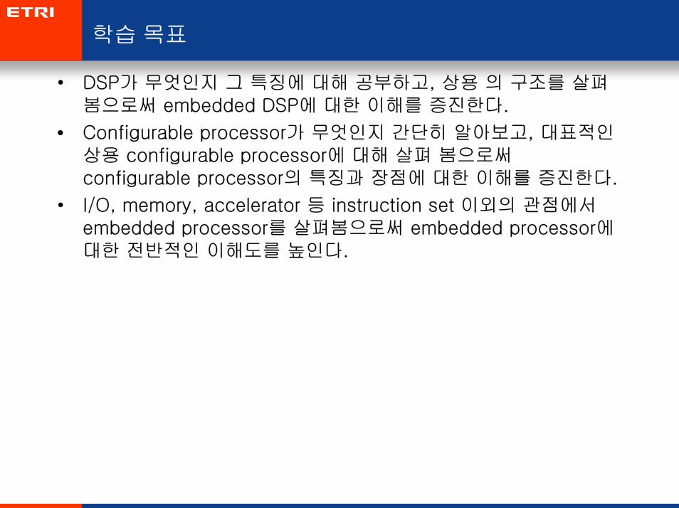
학습목표
• DSP가 무엇인지 그 특징에 대해 공부하고, 상용 의 구조를 살펴봄으로써 embedded DSP에 대한 이해를 증진한다.
• Configurable processor가 무엇인지 간단히 알아보고, 대표적인상용 configurable processor에 대해 살펴 봄으로써configurable processor의 특징과 장점에 대한 이해를 증진한다.
• I/O, memory, accelerator 등 instruction set 이외의 관점에서embedded processor를 살펴봄으로써 embedded processor에대한 전반적인 이해도를 높인다.
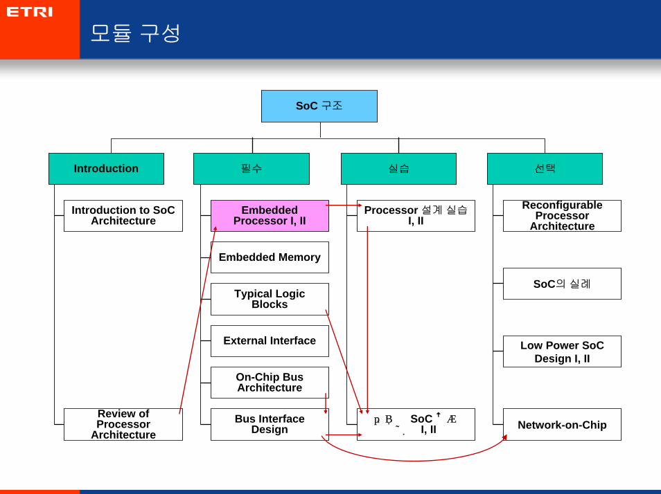
모듈구성
선택필수
SoC 구조
Embedded Processor I, II
Embedded Memory
Typical Logic Blocks
External Interface
On-Chip Bus Architecture
Bus Interface Design
실습
Processor 설계실습I, II
간단한 SoC 설계실습 I, II
Reconfigurable Processor
Architecture
Low Power SoC Design I, II
Network-on-Chip
Introduction
Introduction to SoC Architecture
Review of Processor
Architecture
SoC의실례
강의자료활용 Guideline
• 먼저 "1. DSP"와 "2. CEVA-Teak DSP Architecture"에서는DSP의 개관, 그리고 그 예로 CEVA-Teak DSP를 설명한다. DSP의 예는 다른 것이어도 상관 없으나 GPP와의 차이점이부각되는 예를 들면 좋을 것이다.
• "3. Configurable Processor"와 "4. Tensilica XtensaArchitecture"에서는 configurable processor의 개관과 그 예로Tensilica Xtensa를 설명한다. 주로 Tensilica의 자료를 사용한것으로 간단히 지나가도 좋을 것이다.
• "4. Other Aspects of Embedded Processors"에서는instruction-set architecture와는 조금 다른 관점에서embedded processor에 대해 살펴 보는데, 앞 부분은 기본적이내용이므로 뒷부분의 accelerator에 대해서 중점적으로 강의하면좋을 것이다. "5. ARM OptimoDE Architecture"에서는accelerator의 예로 ARM OptimodDE에 대해서 설명한다.

Contents
1. DSP
2. CEVA-Teak DSP Architecture
3. Configurable Processor
4. Tensilica Xtensa Architecture
5. Other Aspects of Embedded Processors
6. ARM OptimoDE Architecture
7. Summary
8. Exercises
9. References
What are DSPs (Digital Signal Processors)?
• Processors designed for digital signal processing applications
• Examples
– TI TMS320Cx, DaVinci (TMS320DMx)
– Analog Devices SHARC, TigerSHARC, ADSP-21xx
– CEVA CEVA-X16x, Teak, TeakLite
– Adelante Saturn
– Hitachi SH3-DSP
– STMicro ST1x
– StarCore LLC (Freescale, Agere) SC140
– ...
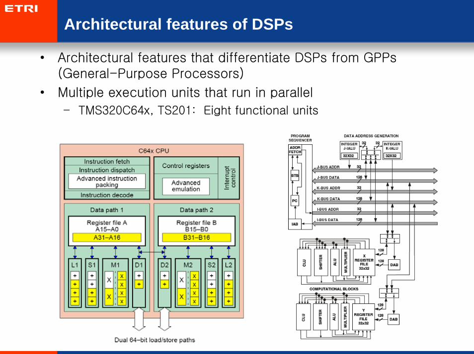
Architectural features of DSPs
• Architectural features that differentiate DSPs from GPPs(General-Purpose Processors)
• Multiple execution units that run in parallel
– TMS320C64x, TS201: Eight functional units
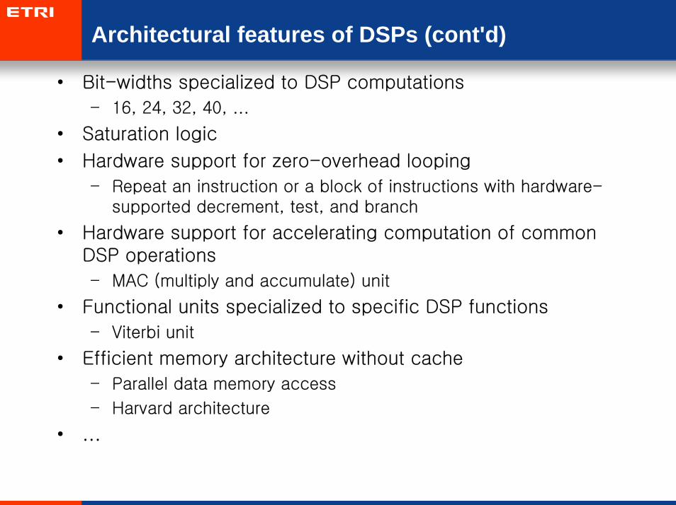
Architectural features of DSPs (cont'd)
• Bit-widths specialized to DSP computations
– 16, 24, 32, 40, ...
• Saturation logic
• Hardware support for zero-overhead looping
– Repeat an instruction or a block of instructions with hardware-supported decrement, test, and branch
• Hardware support for accelerating computation of common DSP operations
– MAC (multiply and accumulate) unit
• Functional units specialized to specific DSP functions
– Viterbi unit
• Efficient memory architecture without cache
– Parallel data memory access
– Harvard architecture
• ...

Contents
1. DSP
2. CEVA-Teak DSP Architecture
3. Configurable Processor
4. Tensilica Xtensa Architecture
5. Other Aspects of Embedded Processors
6. ARM OptimoDE Architecture
7. Summary
8. Exercises
9. References
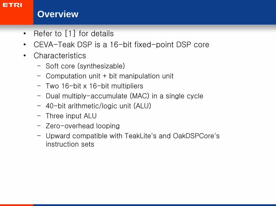
Overview
• Refer to [1] for details
• CEVA-Teak DSP is a 16-bit fixed-point DSP core
• Characteristics
– Soft core (synthesizable)
– Computation unit + bit manipulation unit
– Two 16-bit x 16-bit multipliers
– Dual multiply-accumulate (MAC) in a single cycle
– 40-bit arithmetic/logic unit (ALU)
– Three input ALU
– Zero-overhead looping
– Upward compatible with TeakLite's and OakDSPCore'sinstruction sets
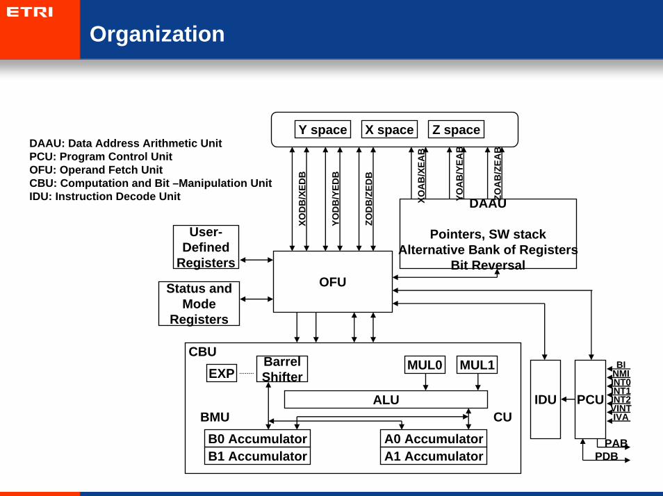
Organization
DAAU: Data Address Arithmetic UnitPCU: Program Control UnitOFU: Operand Fetch UnitCBU: Computation and Bit –Manipulation UnitIDU: Instruction Decode Unit
Y space Z spaceX space
DAAU
Pointers, SW stackAlternative Bank of Registers
Bit ReversalOFU
User-Defined
Registers
Status andMode
Registers
EXPCBU
BMUB0 AccumulatorB1 Accumulator
A0 AccumulatorA1 Accumulator
CU
MUL1
ALU
MUL0BarrelShifter
IDU PCU
BINMIINT0INT1INT2VINTIVA
PABPDB
XOD
B/X
EDB
YOD
B/Y
EDB
ZOD
B/Z
EDB
XOA
B/X
EAB
YOA
B/Y
EAB
ZOA
B/Z
EAB
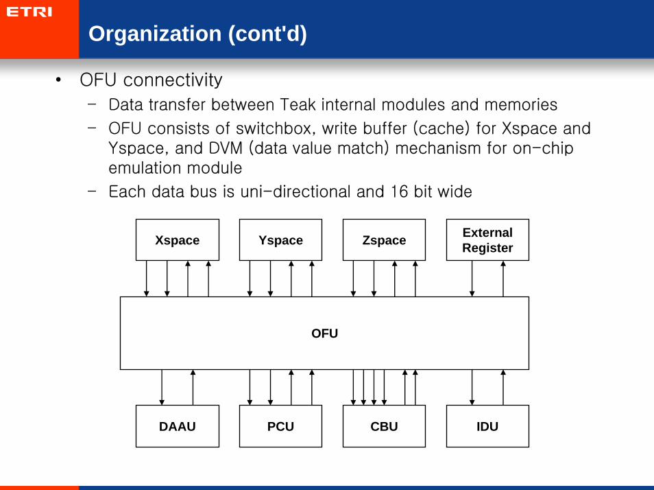
Organization (cont'd)
• OFU connectivity
– Data transfer between Teak internal modules and memories
– OFU consists of switchbox, write buffer (cache) for Xspace and Yspace, and DVM (data value match) mechanism for on-chip emulation module
– Each data bus is uni-directional and 16 bit wide
OFU
Xspace Yspace Zspace ExternalRegister
DAAU PCU CBU IDU

Organization (cont'd)
• Computation and bit-manipulation unit
EXP
a0
ALU
BarrelShifter
Saturation Unit
Saturation Unit
a1 b0 b1
p1MUL1
Scaling Shifter
x y
x1 y1
p0MUL0
Scaling Shifter
y x
y0 x0Bus Align
sign &zero ext.
constconst
sv
YDBXDB/ZDB
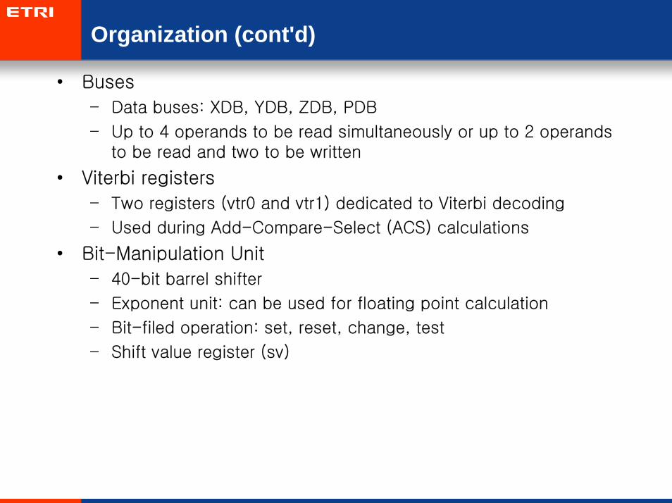
Organization (cont'd)
• Buses
– Data buses: XDB, YDB, ZDB, PDB
– Up to 4 operands to be read simultaneously or up to 2 operands to be read and two to be written
• Viterbi registers
– Two registers (vtr0 and vtr1) dedicated to Viterbi decoding
– Used during Add-Compare-Select (ACS) calculations
• Bit-Manipulation Unit
– 40-bit barrel shifter
– Exponent unit: can be used for floating point calculation
– Bit-filed operation: set, reset, change, test
– Shift value register (sv)
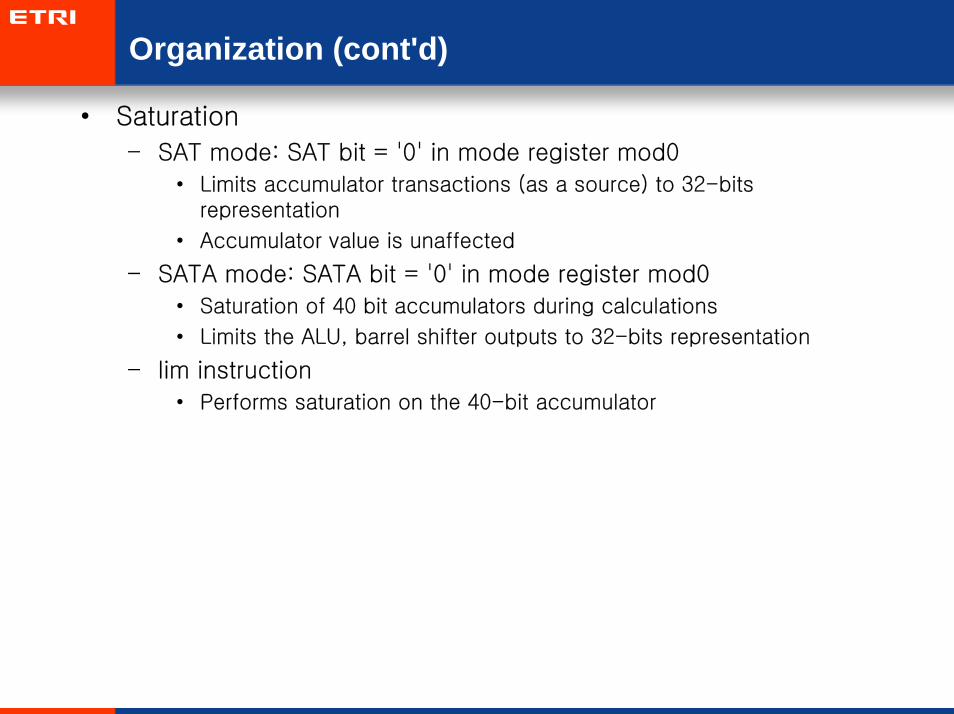
Organization (cont'd)
• Saturation
– SAT mode: SAT bit = '0' in mode register mod0
• Limits accumulator transactions (as a source) to 32-bits representation
• Accumulator value is unaffected
– SATA mode: SATA bit = '0' in mode register mod0
• Saturation of 40 bit accumulators during calculations
• Limits the ALU, barrel shifter outputs to 32-bits representation
– lim instruction
• Performs saturation on the 40-bit accumulator
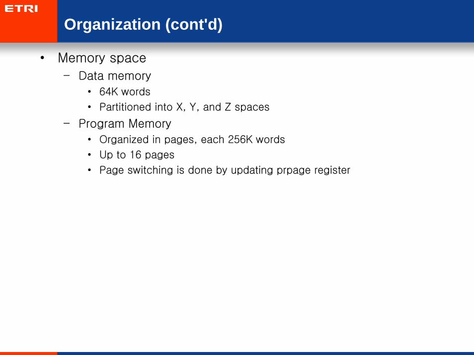
Organization (cont'd)
• Memory space
– Data memory
• 64K words
• Partitioned into X, Y, and Z spaces
– Program Memory
• Organized in pages, each 256K words
• Up to 16 pages
• Page switching is done by updating prpage register
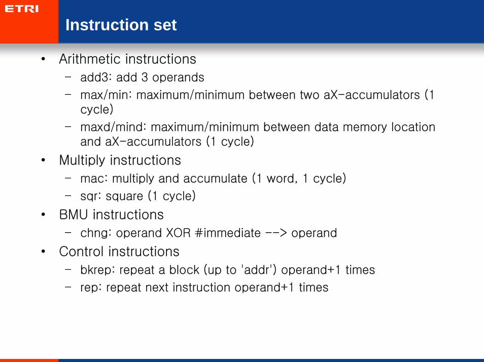
Instruction set
• Arithmetic instructions
– add3: add 3 operands
– max/min: maximum/minimum between two aX-accumulators (1 cycle)
– maxd/mind: maximum/minimum between data memory location and aX-accumulators (1 cycle)
• Multiply instructions
– mac: multiply and accumulate (1 word, 1 cycle)
– sqr: square (1 cycle)
• BMU instructions
– chng: operand XOR #immediate --> operand
• Control instructions
– bkrep: repeat a block (up to 'addr') operand+1 times
– rep: repeat next instruction operand+1 times
Instruction set (cont'd)
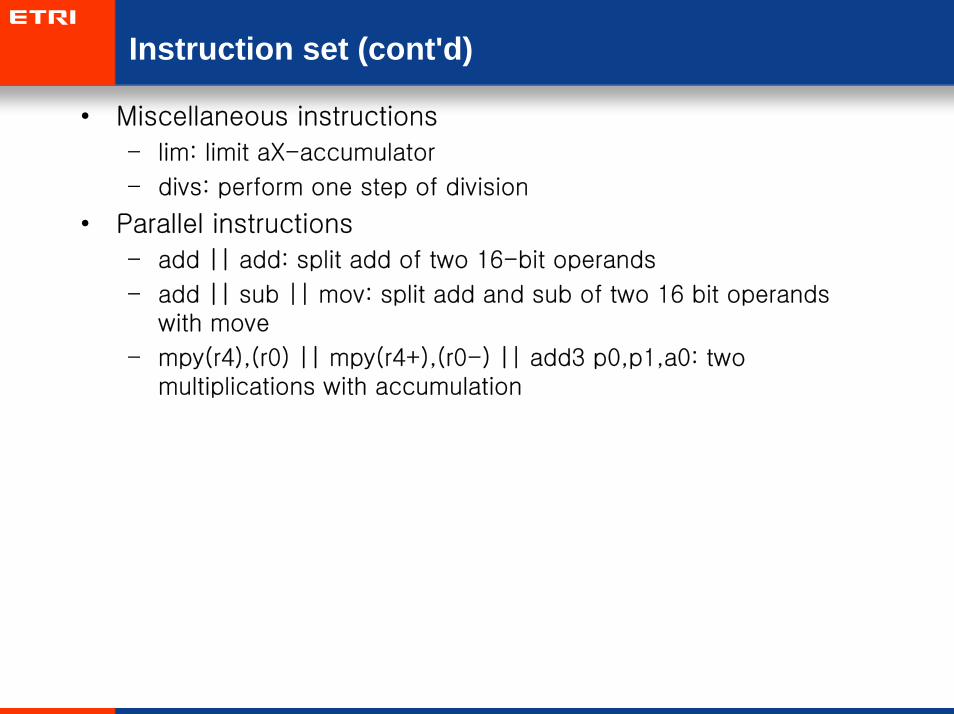
• Miscellaneous instructions
– lim: limit aX-accumulator
– divs: perform one step of division
• Parallel instructions
– add || add: split add of two 16-bit operands
– add || sub || mov: split add and sub of two 16 bit operands with move
– mpy(r4),(r0) || mpy(r4+),(r0-) || add3 p0,p1,a0: two multiplications with accumulation

Contents
1. DSP
2. CEVA-Teak DSP Architecture
3. Configurable Processor
4. Tensilica Xtensa Architecture
5. Other Aspects of Embedded Processors
6. ARM OptimoDE Architecture
7. Summary
8. Exercises
9. References
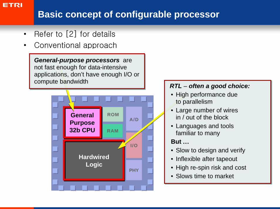
Basic concept of configurable processor
• Refer to [2] for details
• Conventional approach
RAM
ROM
HardwiredLogic
General Purpose 32b CPU
A/D
I/O
PHY
RTL – often a good choice:• High performance due
to parallelism• Large number of wires
in / out of the block• Languages and tools
familiar to manyBut …• Slow to design and verify• Inflexible after tapeout• High re-spin risk and cost• Slows time to market
RTL – often a good choice:• High performance due
to parallelism• Large number of wires
in / out of the block• Languages and tools
familiar to manyBut …• Slow to design and verify• Inflexible after tapeout• High re-spin risk and cost• Slows time to market
General-purpose processors are not fast enough for data-intensive applications, don’t have enough I/O or compute bandwidth
General-purpose processors are not fast enough for data-intensive applications, don’t have enough I/O or compute bandwidth

Basic concept of configurable processor (cont'd)
• Evolution
– More functions per SOC
– Each function more complex
RAM
Data Processing:Data Processing:Image, video, audio, packet processing,
security, or DSPHardwired LogicHardwired Logic
General General ControlControl
RISCRISCControllerController
A/D
I /O
PHY
Silicon scaling
End-product complexity
RAMGeneral General ControlControl
RISCRISCA/D
I/O
PHY
ImageImageLogicLogic
VideoVideoLogicLogic
AudioAudioLogicLogic
VideoVideoLogicLogic
SecuritySecurityLogicLogic
PacketPacketLogicLogic
DSPDSPLogicLogic
System-On-Chip (SOC)Traditional Application-Specific IC (ASIC)
Basic concept of configurable processor (cont'd)
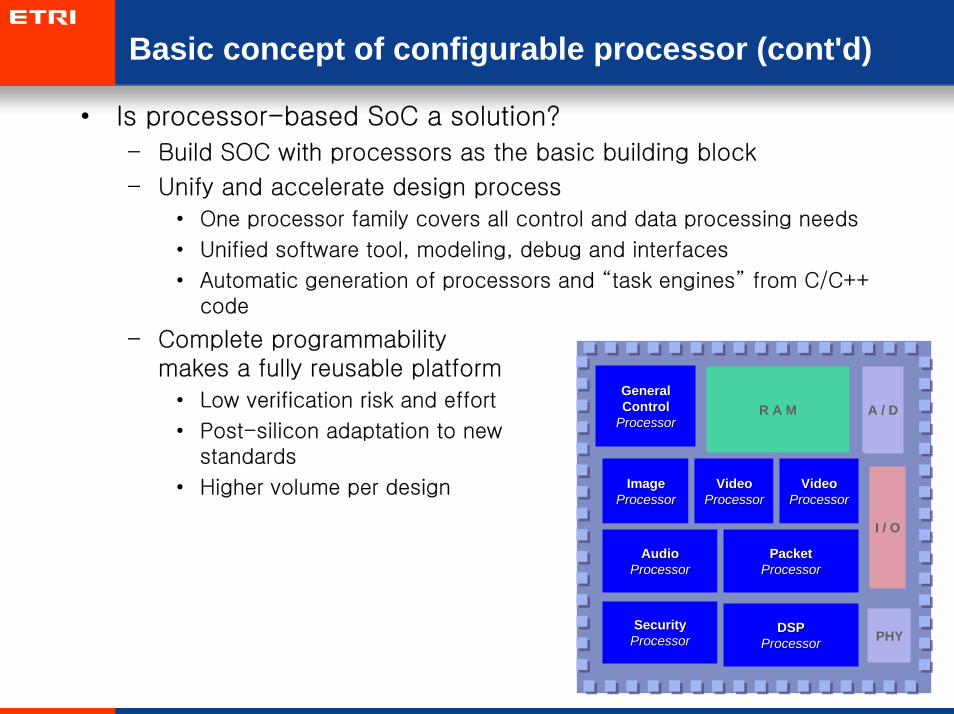
• Is processor-based SoC a solution?
– Build SOC with processors as the basic building block
– Unify and accelerate design process
• One processor family covers all control and data processing needs
• Unified software tool, modeling, debug and interfaces
• Automatic generation of processors and “task engines” from C/C++ code
– Complete programmability makes a fully reusable platform
• Low verification risk and effort
• Post-silicon adaptation to new standards
• Higher volume per design
R A MGeneral General ControlControl
RISCRISCA / D
I / O
PHY
ImageImageLogicLogic
VideoVideoLogicLogic
AudioAudioLogicLogic
VideoVideoLogicLogic
SecuritySecurityLogicLogic
PacketPacketLogicLogic
DSPDSPLogicLogic
General General ControlControl
ProcessorProcessor
ImageImageProcessorProcessor
VideoVideoProcessorProcessor
AudioAudioProcessorProcessor
VideoVideoProcessorProcessor
SecuritySecurityProcessorProcessor
PacketPacketProcessorProcessor
DSPDSPProcessorProcessor
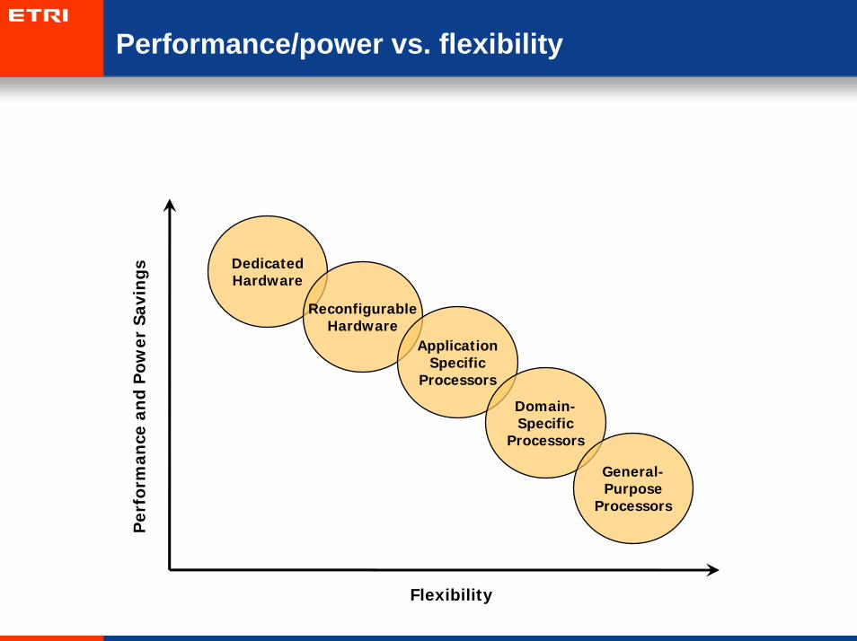
Performance/power vs. flexibility
DedicatedHardware
ReconfigurableHardware
ApplicationSpecific
Processors
Domain-Specific
Processors
General-Purpose
Processors
Per
form
ance
an
d P
ower
Sav
ings
Flexibility
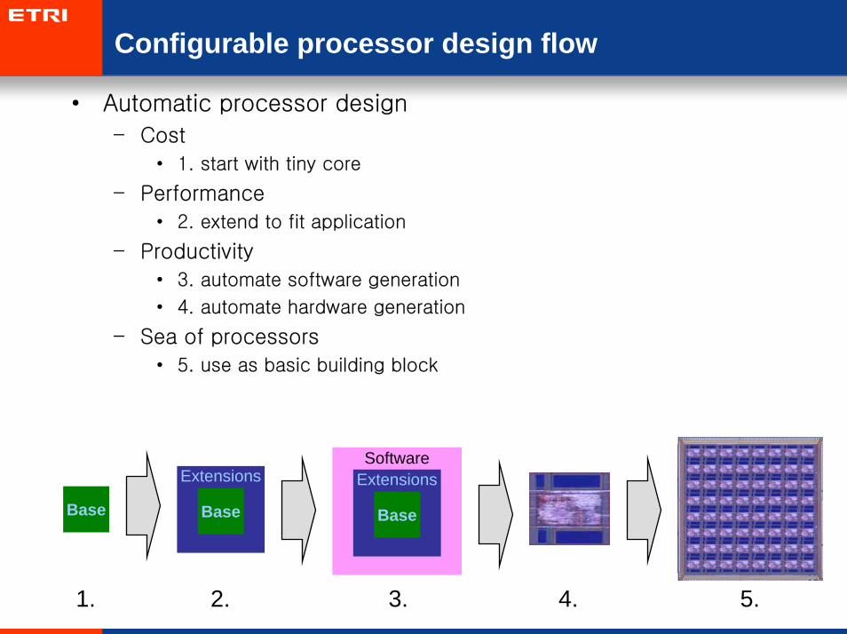
Configurable processor design flow
Base
• Automatic processor design
– Cost
• 1. start with tiny core
– Performance
• 2. extend to fit application
– Productivity
• 3. automate software generation
• 4. automate hardware generation
– Sea of processors
• 5. use as basic building block
1. 2.
Extensions
Base
3.
SoftwareExtensions
Base
4. 5.

Contents
1. DSP
2. CEVA-Teak DSP Architecture
3. Configurable Processor
4. Tensilica Xtensa Architecture
5. Other Aspects of Embedded Processors
6. ARM OptimoDE Architecture
7. Summary
8. Exercises
9. References

Tensilica Xtensa
• Automatic Hardware and Software
Design processor in one hour
High-level specification:
Tensilica Instruction Extension (TIE)
Customized Software Tools:
Compiler, debuggers,
simulators, RTOS
Processor Hardware Design:
RTL, scripts, test benchALU
DSP
OCD
Timer
FPURegister File
Cache
TensilicaProcessorGenerator
Processor configuration
External Interface
Base ISA FeatureConfigurable FunctionOptional Function
User Defined Features (TIE)Optional & Configurable
User Defined Queues and Wires
JTAG Extended Instruction Align, Decode,
Dispatch
Xtensa Processor InterfaceControl
Write Buffer
XtensaLocal Memory Interface
TRACE PortJTAG Tap Control
On Chip Debug
User Defined
Execution Units and Interfaces
Instruction Decode/Dispatch
Base ALU
Floating Point
Vectra DSP
MAC 16 DSPMUL 16/32
User Defined Register
Files
Instruction Fetch / PC
Data Load/Store
Unit
Data ROMs
Data RAMs
DataCache
DataMMU
User Defined
Execution Units
User Defined Register
Files
Vectra DSP
Base Register File
User Defined Execution Unit
Vectra DSP
Processor Controls
Interrupt Control
Data Address Watch Registers
Instruction Address Watch Registers
Timers
Used Defined Data Load/Store Units
Instruction ROMInstruction RAM
InstructionCache
Instruction MMU
PIF
Exception SupportException Handling
Registers
Trace
Interrupts
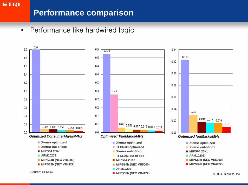
Performance comparison
• Performance like hardwired logic
2.0
0.087 0.080 0.059 0.058 0.0390.0
0.2
0.4
0.6
0.8
1.0
1.2
1.4
1.6
1.8
2.0
Xtensa optimized Xtensa out-of-box MIPS64 20Kc ARM1020E MIPS64b (NEC VR5000) MIPS32b (NEC VR4122)
Optimized ConsumerMarks/MHz
0.473
0.03 0.023 0.016 0.013 0.011
0.23
0.017
0.0
0.1
0.1
0.2
0.2
0.3
0.3
0.4
0.4
0.5
0.5
Xtensa optimized TI C6203 optimized Xtensa out-of-box TI C6203 out-of-box MIPS64 20Kc MIPS64b (NEC VR5000) ARM1020E MIPS32b (NEC VR4122)
Optimized TeleMarks/MHz
0.123
0.03
0.018 0.017 0.0160.01
0.00
0.02
0.04
0.06
0.08
0.10
0.12
0.14
Xtensa optimized Xtensa out-of-box MIPS64 20Kc ARM1020E MIPS64b (NEC VR5000) MIPS32b (NEC VR4122)
Optimized NetMarks/MHz
Source: EEMBC© 2004, Tensilica, Inc.

Code size and core size comparison
243968
7032859648 57149
387328
0
100000
200000
300000
400000
Cod
e B
ytes
Trimedia TM1300 optimized Trimedia TM1300 out-of-boxARM1020E Xtensa optimizedXtensa out-of-box
0
5
10
15
20
25
30
35
optimized out-of-box optimized out-of-box
Xtensa Xtensa Trimedia TM1300 Trimedia TM1300
core
+ c
ode
area
mm
2 (0.1
3 µ)
core area code area
EEMBC ConsumerMark
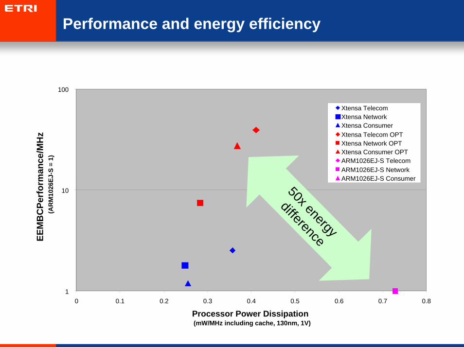
Performance and energy efficiency
1
10
100
0 0.1 0.2 0.3 0.4 0.5 0.6 0.7 0.8
Processor Power Dissipation (mW/MHz including cache, 130nm, 1V)
EEM
BC
Perf
orm
ance
/MH
z (A
RM
1026
EJ-S
= 1
)
Xtensa TelecomXtensa NetworkXtensa ConsumerXtensa Telecom OPTXtensa Network OPTXtensa Consumer OPTARM1026EJ-S Telecom ARM1026EJ-S Network ARM1026EJ-S Consumer
50x energy
difference

Design space exploration
• Xtensa PRocessor Extension Synthesis (XPRES)
Option: manually refine configuration
Original C/C++ Code
Evaluates millions of possible extensions:
• SIMD operations
• operator fusion
• parallel execution
Designer selects “best”
configurationRun XPRES
Compiler
int main(){int i;short c[100];for (i=0;i<N/2;i++){
int main(){int i;short c[100];for (i=0;i<N/2;i++){
Xtensa Processor Generator
Tuned Software Tools
Processor Hardware
ALU
DSP
OCD
Timer
FPURegister File
Cache
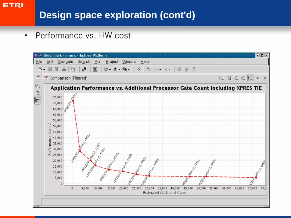
Design space exploration (cont'd)
• Performance vs. HW cost

Contents
1. DSP
2. CEVA-Teak DSP Architecture
3. Configurable Processor
4. Tensilica Xtensa Architecture
5. Other Aspects of Embedded Processors
6. ARM OptimoDE Architecture
7. Summary
8. Exercises
9. References

Introduction
• Refer to [3] for details
• Aspects that do not directly relate to instruction sets
– Input and output
– Coprocessor
– Cache
– Memory management and address translation
– Accelerator
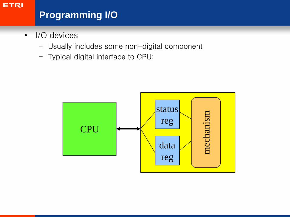
Programming I/O
• I/O devices
– Usually includes some non-digital component
– Typical digital interface to CPU:
CPU
statusreg
datareg m
echa
nism
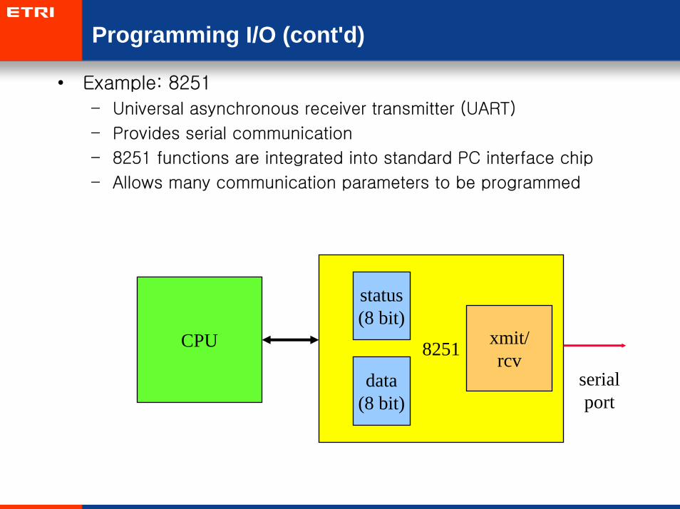
Programming I/O (cont'd)
• Example: 8251
– Universal asynchronous receiver transmitter (UART)
– Provides serial communication
– 8251 functions are integrated into standard PC interface chip
– Allows many communication parameters to be programmed
CPU 8251
status(8 bit)
data(8 bit)
xmit/rcv
serialport
Programming I/O (cont'd)
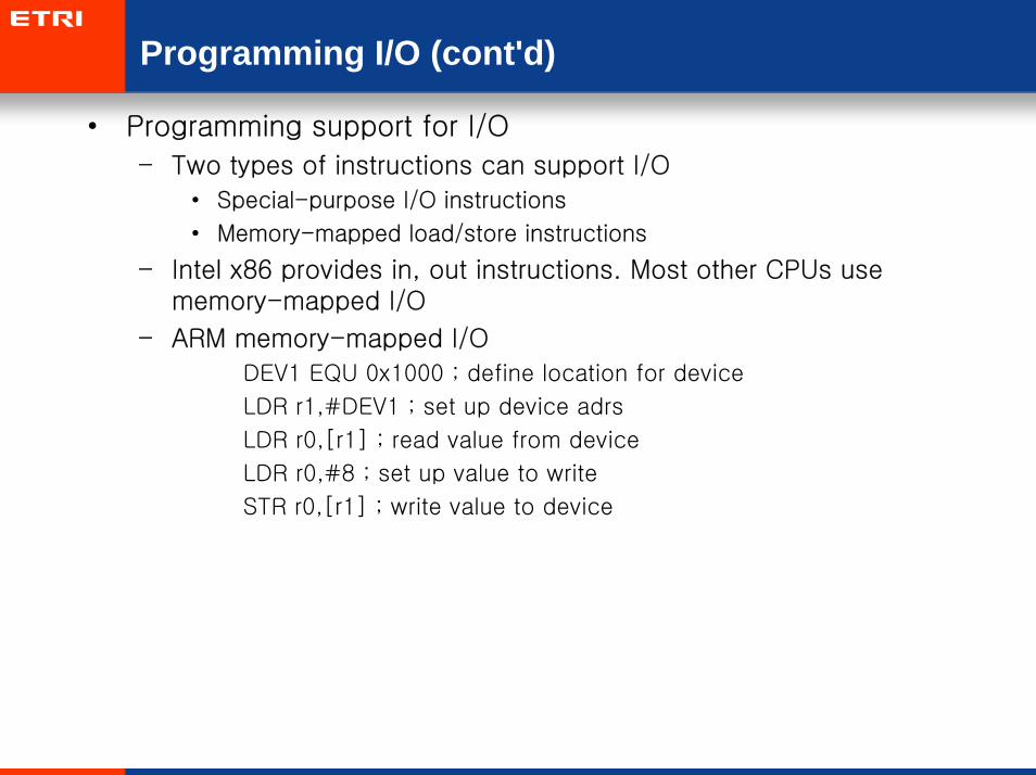
• Programming support for I/O
– Two types of instructions can support I/O
• Special-purpose I/O instructions
• Memory-mapped load/store instructions
– Intel x86 provides in, out instructions. Most other CPUs use memory-mapped I/O
– ARM memory-mapped I/O
DEV1 EQU 0x1000 ; define location for device
LDR r1,#DEV1 ; set up device adrs
LDR r0,[r1] ; read value from device
LDR r0,#8 ; set up value to write
STR r0,[r1] ; write value to device
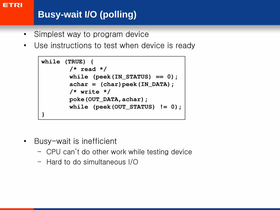
Busy-wait I/O (polling)
• Simplest way to program device
• Use instructions to test when device is ready
• Busy-wait is inefficient
– CPU can’t do other work while testing device
– Hard to do simultaneous I/O
while (TRUE) {/* read */while (peek(IN_STATUS) == 0);achar = (char)peek(IN_DATA);/* write */poke(OUT_DATA,achar);while (peek(OUT_STATUS) != 0);
}
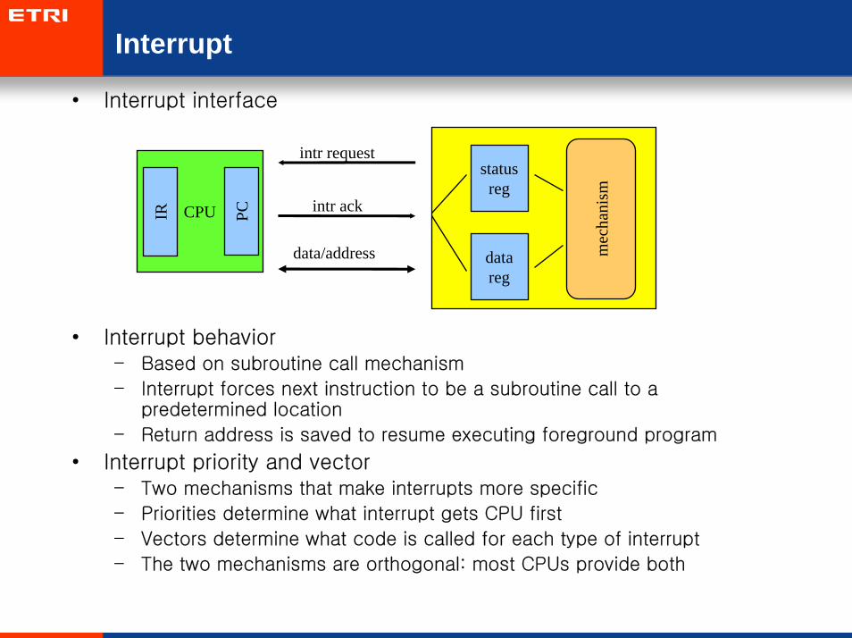
Interrupt
• Interrupt interface
• Interrupt behavior– Based on subroutine call mechanism
– Interrupt forces next instruction to be a subroutine call to a predetermined location
– Return address is saved to resume executing foreground program
• Interrupt priority and vector– Two mechanisms that make interrupts more specific
– Priorities determine what interrupt gets CPU first
– Vectors determine what code is called for each type of interrupt
– The two mechanisms are orthogonal: most CPUs provide both
statusreg
datareg
mec
hani
sm
intr request
CPUIR PC intr ack
data/address

Interrupt (cont'd)
• Interrupt priority
– Masking: interrupt with priority lower than current priority is not recognized until pending interrupt is complete
– Non-maskable interrupt (NMI):
• Highest-priority, never masked
• Often used for power-down
CPU
device 1 device 2 device n
L1 L2 .. Ln
interruptacknowledge

Interrupt (cont'd)
• Interrupt vector
– Allow different devices to be handled by different code
– Interrupt vector table:
Device
CPU
Vector
interruptacknowledge
interruptrequest
Interruptvector
table headhandler 0
handler 1
handler 2
handler 3

Interrupt (cont'd)
• Interrupt sequence
– CPU acknowledges request
– Device sends vector
– CPU calls handler
– Software processes request
– CPU restores state to foreground program
• Sources of interrupt overhead
– Handler execution time
– Interrupt mechanism overhead
– Register save/restore
– Pipeline-related penalties
– Cache-related penalties

Interrupt (cont'd)
• ARM interrupts
– Supports two types of interrupt
• Fast interrupt request (FIQ)
• Interrupt request (IRQ)
– Interrupt procedure
• CPU actions on interrupt
– Save PC and copy CPSR to SPSR
– Force bits in CPSR to record interrupt
– Force PC to vector
• Handler responsibilities on return
– Restore proper PC
– Restore CPSR from SPSR
– Clear interrupt disable flags
– Interrupt latency
• Latency to respond to interrupt can be up to 27 cycles and as low as 4 cycles (ARM7TDMI-S)

Coprocessor
• Added function unit that is called by instruction
– Floating-point units are often structured as coprocessors
• ARM allows up to 16 designer-selected coprocessors
– Floating-point coprocessor uses units 1 and 2
ARM Memorysystem
Coprocessor
RDATA
WDATA
bsel
asel
csel
CPDIN CPDOUT
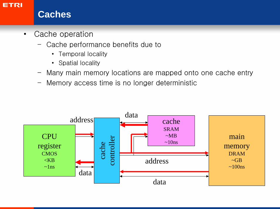
Caches
• Cache operation
– Cache performance benefits due to
• Temporal locality
• Spatial locality
– Many main memory locations are mapped onto one cache entry
– Memory access time is no longer deterministic
CPUregister
CMOS<KB~1ns
cach
eco
ntro
ller
cacheSRAM~MB~10ns
mainmemory
DRAM~GB
~100ns
data
data
addressdata
address
Caches (cont'd)
• May have caches for
– instructions
– data
– data + instructions (unified)
• ARM920T
– 16 Kbyte, 64-way, 32-byte block instruction cache
– 16 Kbyte, 64-way, 32-byte block data cache (write-through and write-back)
– random or round-robin replacement
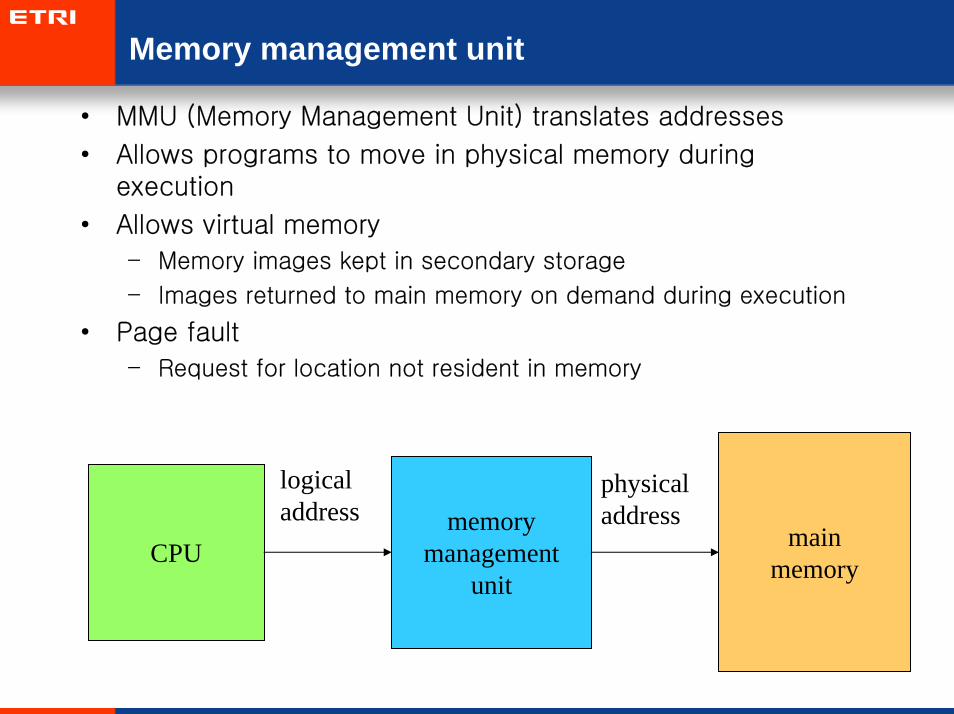
Memory management unit
• MMU (Memory Management Unit) translates addresses
• Allows programs to move in physical memory during execution
• Allows virtual memory
– Memory images kept in secondary storage
– Images returned to main memory on demand during execution
• Page fault
– Request for location not resident in memory
CPU mainmemory
memorymanagement
unit
logicaladdress
physicaladdress
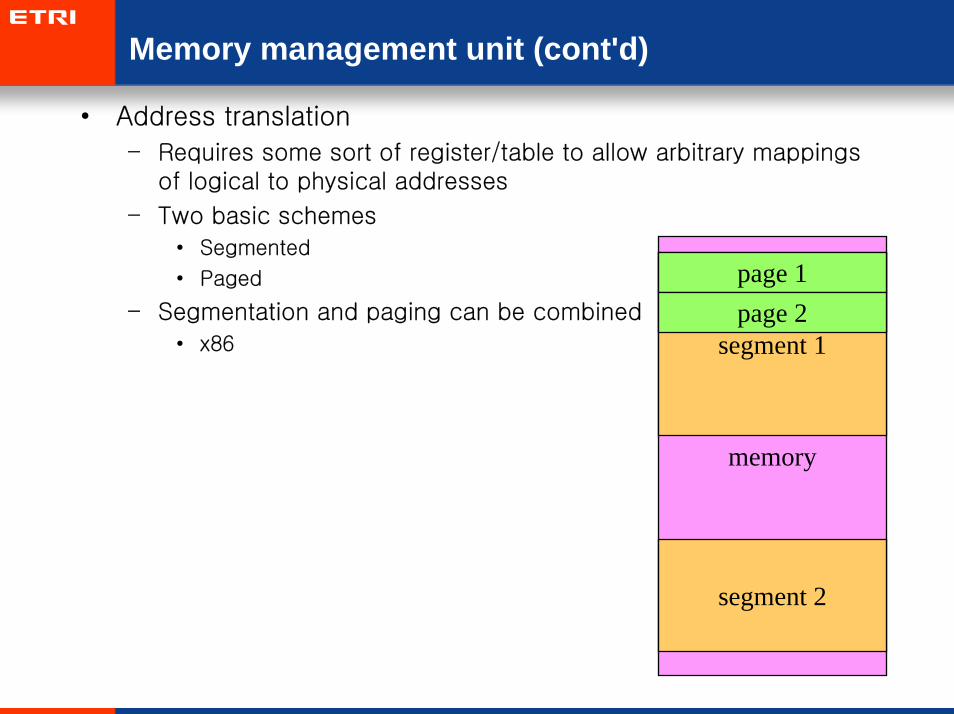
Memory management unit (cont'd)
• Address translation
– Requires some sort of register/table to allow arbitrary mappingsof logical to physical addresses
– Two basic schemes
• Segmented
• Paged
– Segmentation and paging can be combined
• x86
memory
segment 1
segment 2
page 1page 2
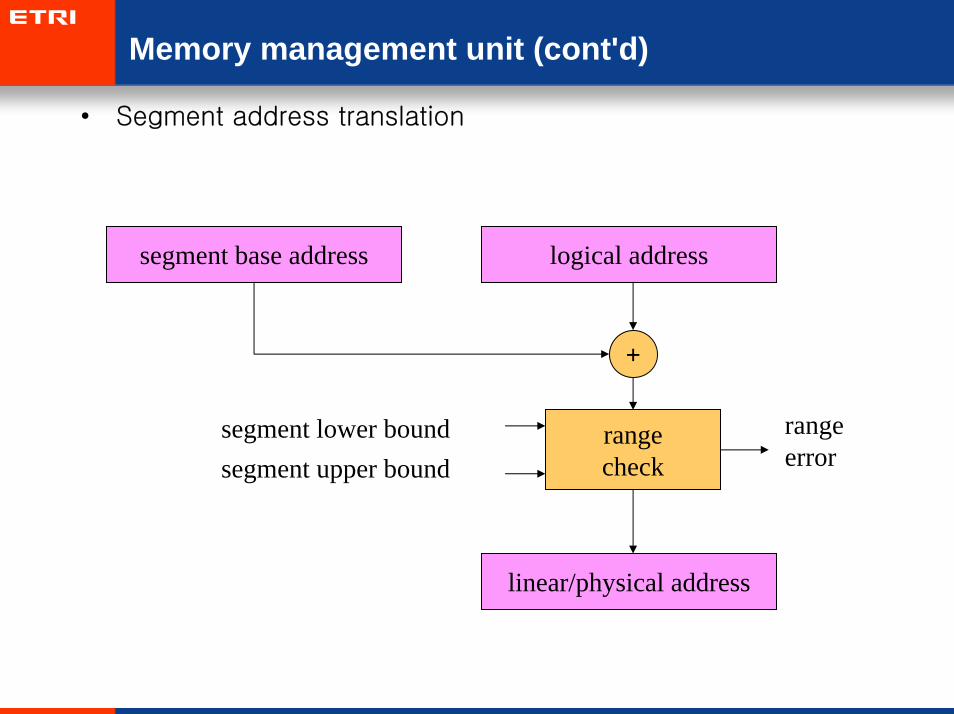
Memory management unit (cont'd)
• Segment address translation
segment base address logical address
rangecheck
linear/physical address
+
rangeerror
segment lower boundsegment upper bound
Memory management unit (cont'd)
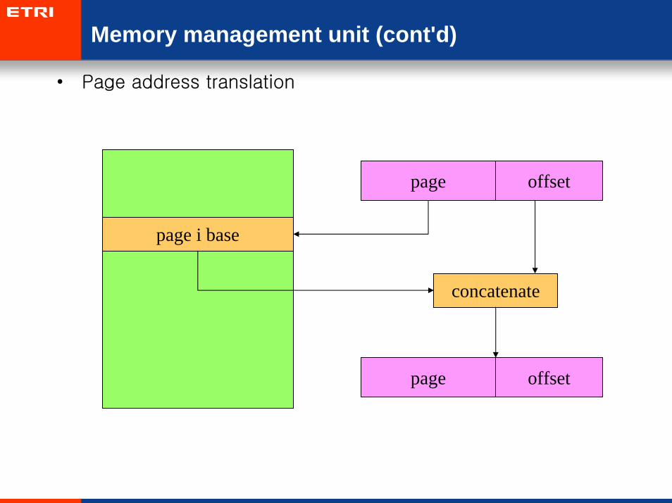
• Page address translation
page offset
page offset
page i base
concatenate

Memory management unit (cont'd)
• Page table organizations
• Caching address translations
– Large translation tables require main memory access
– TLB (Translation Look-aside Buffer)
• Cache for address translation
• Typically small
flat tree
page descriptor
pagedescriptor

Memory management unit (cont'd)
• ARM memory management
– Memory region types
• section: 1 Mbyte block
• large page: 64 Kbytes
• small page: 4 Kbytes
• tiny page: 1 Kbytes
– An address is marked as section-mapped or page-mapped
– Two-level translation scheme
offset1st index 2nd index
physical address
Translation tablebase register
1st level tabledescriptor
2nd level tabledescriptor
concatenate
concatenate
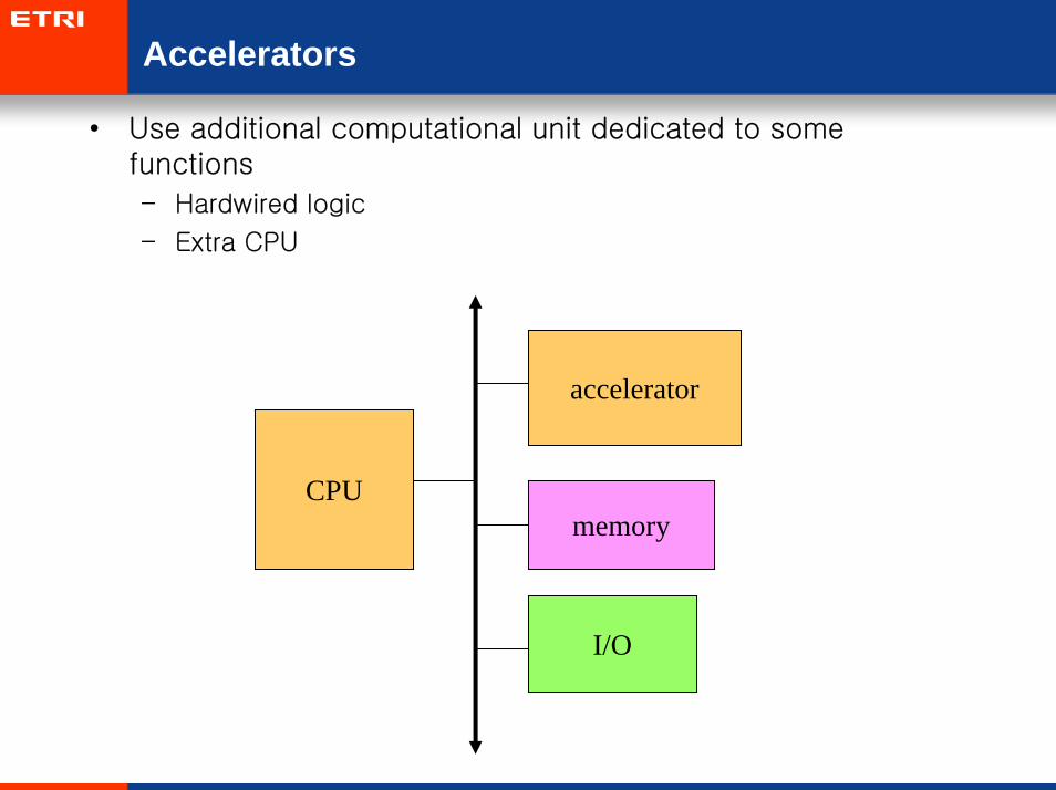
Accelerators
• Use additional computational unit dedicated to some functions
– Hardwired logic
– Extra CPU
CPU
accelerator
memory
I/O
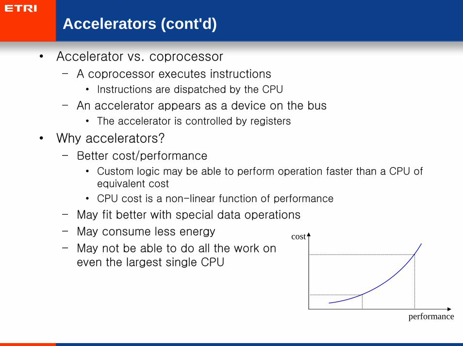
Accelerators (cont'd)
• Accelerator vs. coprocessor
– A coprocessor executes instructions
• Instructions are dispatched by the CPU
– An accelerator appears as a device on the bus
• The accelerator is controlled by registers
• Why accelerators?
– Better cost/performance
• Custom logic may be able to perform operation faster than a CPU of equivalent cost
• CPU cost is a non-linear function of performance
– May fit better with special data operations
– May consume less energy
– May not be able to do all the work on even the largest single CPU
cost
performance
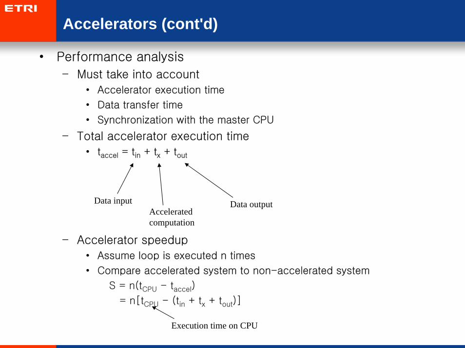
Accelerators (cont'd)
• Performance analysis
– Must take into account
• Accelerator execution time
• Data transfer time
• Synchronization with the master CPU
– Total accelerator execution time
• taccel = tin + tx + tout
– Accelerator speedup
• Assume loop is executed n times
• Compare accelerated system to non-accelerated system
S = n(tCPU - taccel)
= n[tCPU - (tin + tx + tout)]
Data inputAcceleratedcomputation
Data output
Execution time on CPU
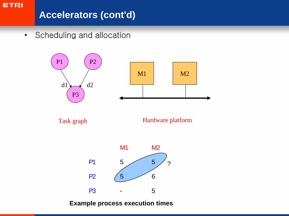
Accelerators (cont'd)
• Scheduling and allocation
P1 P2
P3d1 d2
Task graph Hardware platform
M1 M2
M1 M2
P1 5 5
P2 5 6
P3 - 5
Example process execution times
?

Accelerators (cont'd)
– Assume communication within PE is free
– Cost of communication
• P1->P3: d1 =2
• P2->P3: d2 = 4
P1 P2
P3
d1=2 d2=4
Task graph
Accelerators (cont'd)
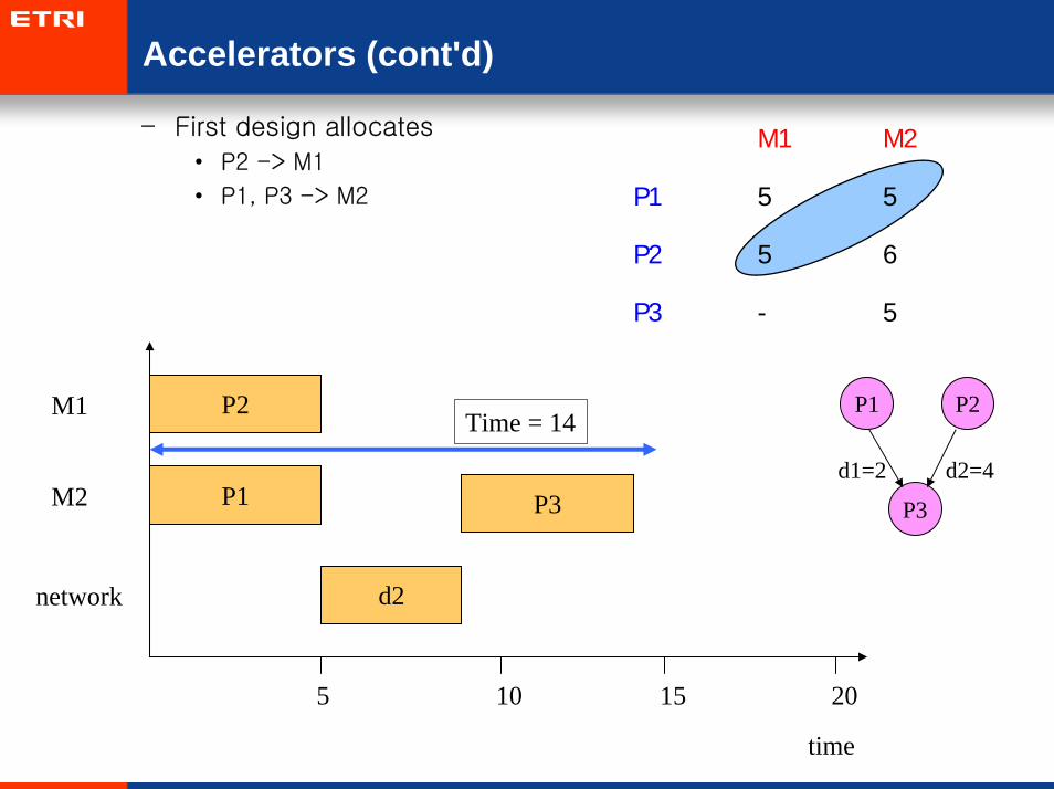
– First design allocates
• P2 -> M1
• P1, P3 -> M2
M1 M2
P1 5 5
P2 5 6
P3 - 5
P2 P1 P2
P3
d1=2 d2=4
M1
time
M2
network
5 10 15 20
P1
d2
P3
Time = 14
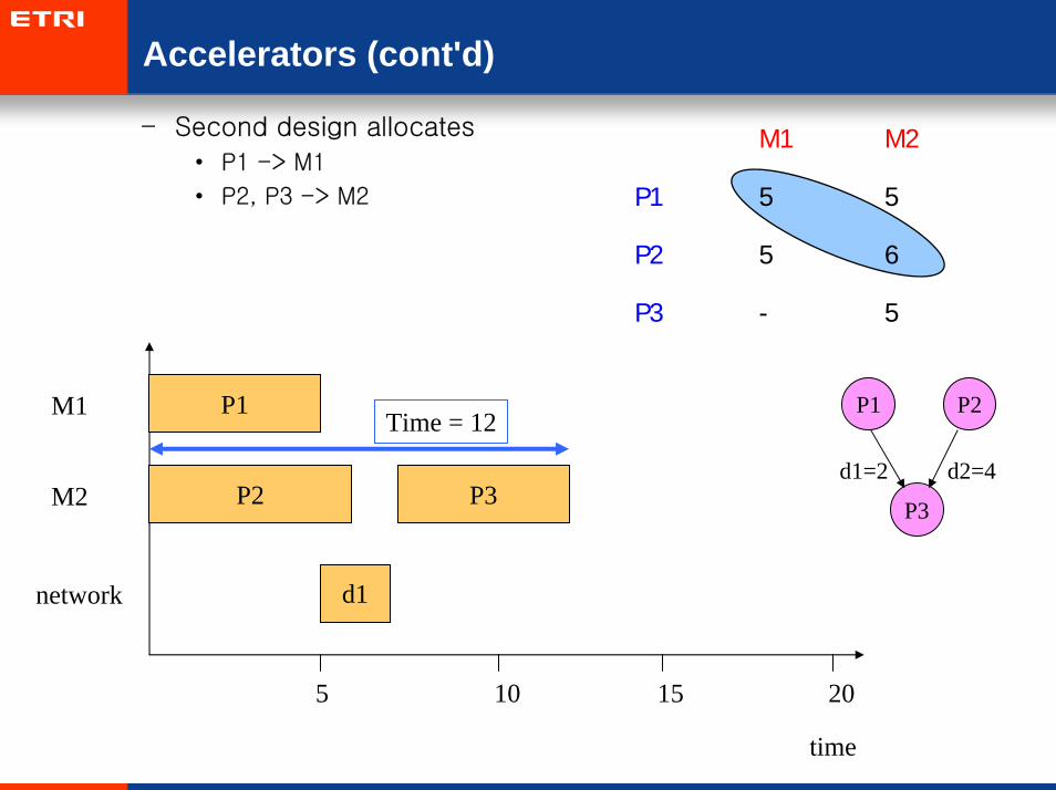
Accelerators (cont'd)
– Second design allocates
• P1 -> M1
• P2, P3 -> M2
M1 M2
P1 5 5
P2 5 6
P3 - 5
P1 P1 P2
P3
d1=2 d2=4
M1
M2
network
5 10 15 20
P2
d1
P3
Time = 12
time

Contents
1. DSP
2. CEVA-Teak DSP Architecture
3. Configurable Processor
4. Tensilica Xtensa Architecture
5. Other Aspects of Embedded Processors
6. ARM OptimoDE Architecture
7. Summary
8. Exercises
9. References
Overview
• Refer to [4] for details
• OptimoDE is
– A configurable VLIW-styled Data Engine architecture
– Targeted at intensive data processing
• Characteristics
– Very wide performance envelope
• Power / area / speed tradeoff
• Exploiting parallelism in applications
– Unlimited data path configuration options
– User extensible through ISA customization
• Semi-automatic design system
– User-in-the-loop design, retargetable compiler toolchain
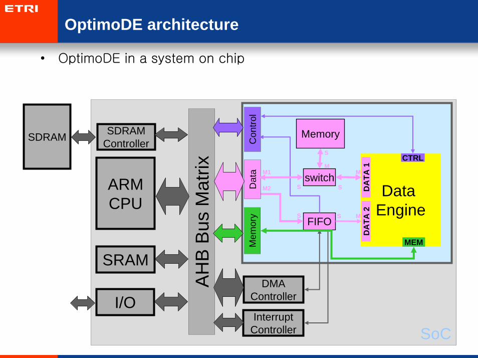
OptimoDE architecture
• OptimoDE in a system on chip
SDRAM
SoC
AH
B B
us M
atrix
ARMCPU
DMAController
InterruptController
SRAM
I/O
SDRAMController
Mem
ory
Con
trol
DataEngine
DA
TA 1
MEM
CTRL
DA
TA 2
FIFO
switch
Memory
Dat
a M1
M2
M
S
S S
M
S S M
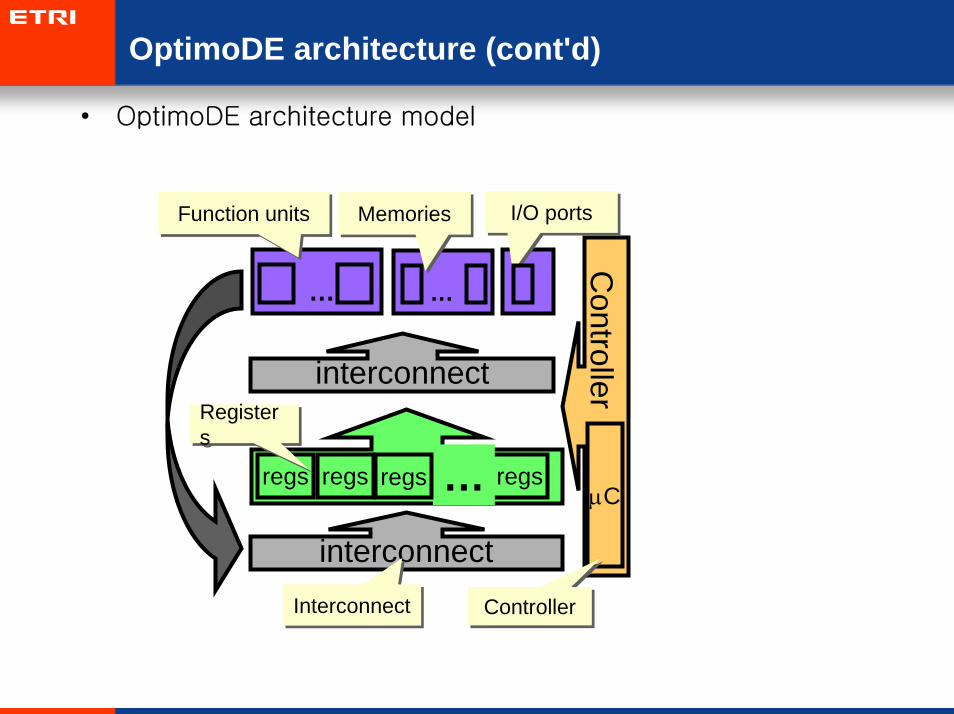
OptimoDE architecture (cont'd)
• OptimoDE architecture model
interconnect
InterconnectInterconnect
Controller
µC
ControllerController
interconnect
… …
Function unitsFunction units MemoriesMemories
regs regs regs…regs
I/O portsI/O ports
RegistersRegisters

OptimoDE architecture (cont'd)
• 32-point DCT microarchitecture
inport
outportacu_1 acu_2 acu_3
romram_1 ram_2 alu_1 alu_2
imm_1 imm_2 control
• 2 Custom FUs, 2 RAM, 1 ROM, 3 ACU, 2 I/O ports• Designer responsible for creating custom units manually
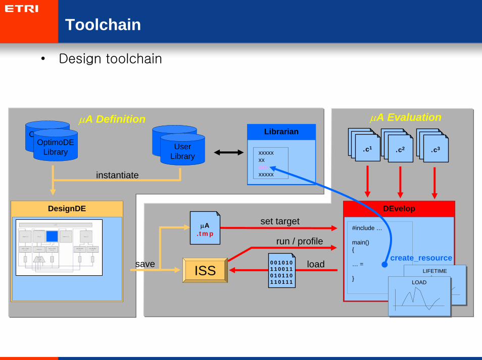
Toolchain
• Design toolchain
µA.tmp
DesignDE DEvelop
Librarian
save ISS
set target
001010110011010110110111
load
run / profile
µA.incµA
.inc.c1
UserLibrary
instantiate
#include …
main(){
… = dct();
}
create_resource
xxxxxxxdctxxxxx
µA.incµA
.inc.c2
µA.incµA
.inc.c3
µA EvaluationOptimoDE
LibraryOptimoDELibrary
UserLibrary
µA Definition
LIFETIMELIFETIME
LOADLOAD
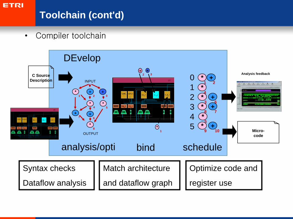
Toolchain (cont'd)
• Compiler toolchain
*1
+2
*4
*5
+6
+7
*8
INPUT
OUTPUT
+3
*1
+2
+3 0
12345
+2
*1
*4
*3
+6
*8
+7
*5
*9
+10
C SourceDescription
DEvelop
Micro-code
analysis/opti bind schedule
Analysis feedback
Syntax checks
Dataflow analysis
Match architecture
and dataflow graph
Optimize code and
register use

Creating custom instructions
• Candidate discovery
– Identify customization opportunities
• Examine program DFG
• Partition DFG at:
– Memory operations
– Unprofitable edges
• Enumerate candidate subgraphs within each partition
Creating custom instructions (cont'd)
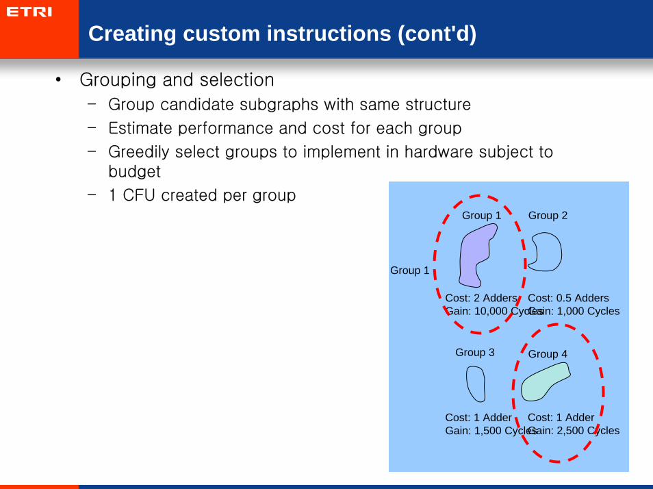
• Grouping and selection
– Group candidate subgraphs with same structure
– Estimate performance and cost for each group
– Greedily select groups to implement in hardware subject to budget
– 1 CFU created per group
Group 4
Group 2
Group 3
Group 4Group 3
Group 1 Group 2
Cost: 0.5 AddersGain: 1,000 Cycles
Cost: 1 AdderGain: 2,500 Cycles
Cost: 2 AddersGain: 10,000 Cycles
Cost: 1 AdderGain: 1,500 Cycles
Group 1
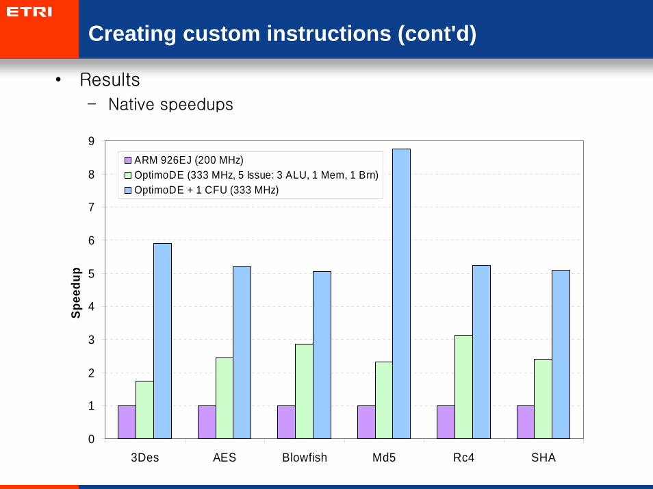
Creating custom instructions (cont'd)
• Results
– Native speedups
0
1
2
3
4
5
6
7
8
9
3Des AES Blowfish Md5 Rc4 SHA
Spee
dup
ARM 926EJ (200 MHz)OptimoDE (333 MHz, 5 Issue: 3 ALU, 1 Mem, 1 Brn)OptimoDE + 1 CFU (333 MHz)
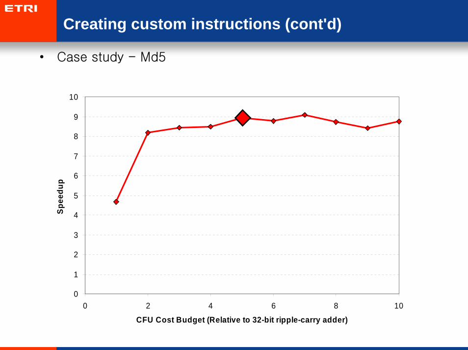
Creating custom instructions (cont'd)
• Case study - Md5
0
1
2
3
4
5
6
7
8
9
10
0 2 4 6 8 10
CFU Cost Budget (Relative to 32-bit ripple-carry adder)
Spee
dup
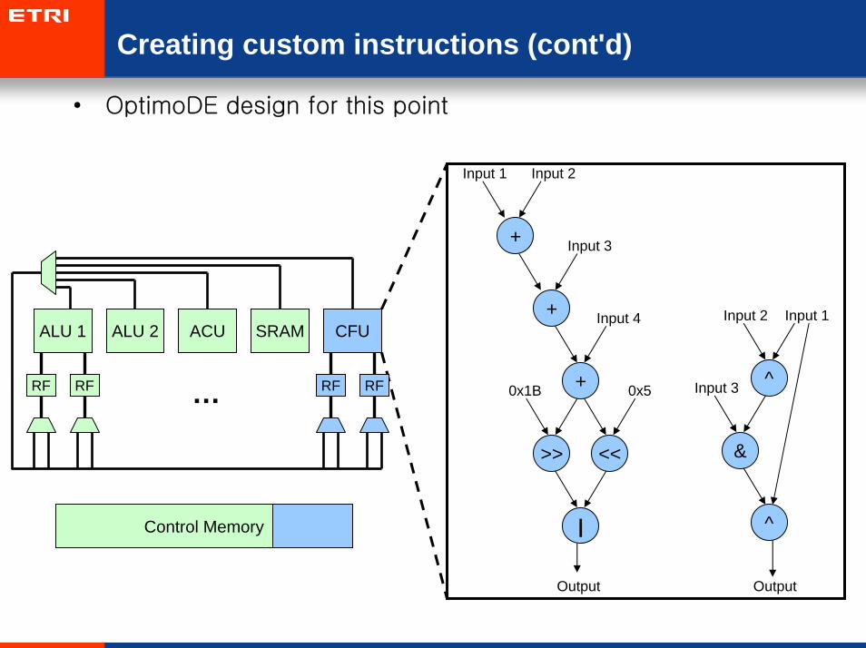
Creating custom instructions (cont'd)
• OptimoDE design for this point
Input 4
Input 1
Input 3
Input 2
+
+
+
<<
0x5
>>
0x1B
|
Output
^
&
^
Input 1Input 2
Input 3
Output
ALU 1 ALU 2 CFUSRAMACU
RF RFRF RF …
Control Memory
Creating custom instructions (cont'd)
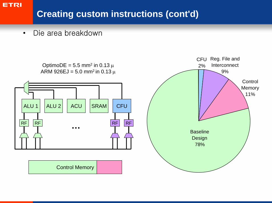
• Die area breakdown
Reg. File and Interconnect
9%
CFU2%
Control Memory
11%
Baseline Design
78%
OptimoDE = 5.5 mm2 in 0.13 µARM 926EJ = 5.0 mm2 in 0.13 µ
ALU 1 ALU 2 CFUSRAMACU
RF RFRF RF …
Control Memory
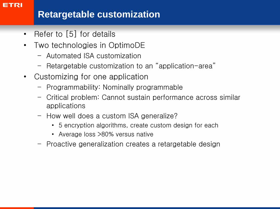
Retargetable customization
• Refer to [5] for details
• Two technologies in OptimoDE
– Automated ISA customization
– Retargetable customization to an “application-area”
• Customizing for one application
– Programmability: Nominally programmable
– Critical problem: Cannot sustain performance across similar applications
– How well does a custom ISA generalize?
• 5 encryption algorithms, create custom design for each
• Average loss >80% versus native
– Proactive generalization creates a retargetable design
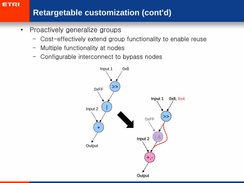
Retargetable customization (cont'd)
• Proactively generalize groups
– Cost-effectively extend group functionality to enable reuse
– Multiple functionality at nodes
– Configurable interconnect to bypass nodes
Input 2
Input 1
0xFF
0x8, 0x40x4
>>
|,&
+,-
Output
Input 2
Input 1
0xFF
0x8
>>
|
+
Output
Input 2
Input 1
0xFF
0x8, 0x40x4
>>
|,&
+,-
Output
Retargetable customization (cont'd)
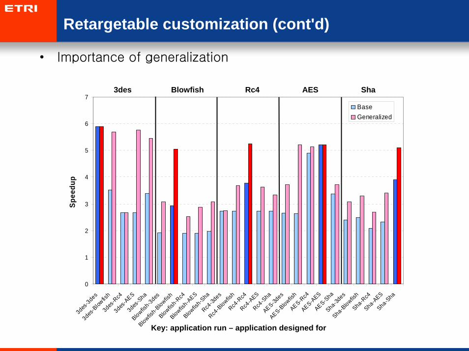
• Importance of generalization
0
1
2
3
4
5
6
7
3des
-3des
3des
-Blow
fish
3des
-Rc4
3des
-AES
3des
-Sha
Blowfish-3d
es
Blowfish-B
lowfis
h
Blowfish-R
c4
Blowfish-A
ES
Blowfish-S
haRc4
-3des
Rc4-B
lowfis
hRc4
-Rc4
Rc4-A
ESRc4
-Sha
AES-3des
AES-Blowfis
hAES-R
c4AES-A
ESAES-S
haSha
-3des
Sha-B
lowfis
hSha
-Rc4
Sha-A
ESSha
-Sha
Spee
dup
BaseGeneralized
0
1
2
3
4
5
6
7
3des
-3des
3des
-Blow
fish
3des
-Rc4
3des
-AES
3des
-Sha
Blowfish-3d
es
Blowfish-B
lowfis
h
Blowfish-R
c4
Blowfish-A
ESBlowfis
h-Sha
Rc4-3d
es
Rc4-B
lowfis
hRc4
-Rc4
Rc4-A
ESRc4
-Sha
AES-3des
AES-Blowfis
hAES-R
c4AES-A
ESAES-S
haSha
-3des
Sha-B
lowfis
hSha
-Rc4
Sha-A
ESSha
-Sha
Spee
dup
BaseGeneralized
0
1
2
3
4
5
6
7
3des-3des
3des-B
lowfis
h3des
-Rc4
3des-A
ES3des
-Sha
Blowfish-3des
Blowfish-B
lowfish
Blowfish-R
c4
Blowfish-A
ESBlowfis
h-Sha
Rc4-3d
esRc4
-Blowfis
hRc4
-Rc4
Rc4-A
ESRc4
-Sha
AES-3des
AES-Blowfis
hAES-R
c4AES-A
ESAES-S
haSha-3d
esSha-B
lowfish
Sha-Rc4
Sha-AES
Sha-Sha
Spee
dup
BaseGeneralized
Key: application run – application designed for
3des Blowfish Rc4 AES Sha

Contents
1. DSP
2. CEVA-Teak DSP Architecture
3. Configurable Processor
4. Tensilica Xtensa Architecture
5. Other Aspects of Embedded Processors
6. ARM OptimoDE Architecture
7. Summary
8. Exercises
9. References
Summary
• A typical DSP has multiple functional units that run in paralleland supports saturation logic and hardware looping.
• Configurable processors can be optimized to applications to achieve better performance with less area power at the cost of some flexibility.
• Accelerator is a good way of achieving performance while maintaining flexibility of the embedded processor.

Contents
1. DSP
2. CEVA-Teak DSP Architecture
3. Configurable Processor
4. Tensilica Xtensa Architecture
5. Other Aspects of Embedded Processors
6. ARM OptimoDE Architecture
7. Summary
8. Exercises
9. References
Exercises
1. Explain the reason why DSPs support zero-overhead looping while GPPs such as ARM do not?
2. Xtensa processor optimized to a specific application look superior to other processors in every aspect. Does this mean Xtensa processors can replace other processors in every embedded system? Explain your answer.
3. Many embedded systems today use multiple processor core and/or hardware blocks. Explain the reason why they do not use just one fast processor that handles all tasks?
Contents
1. DSP
2. CEVA-Teak DSP Architecture
3. Configurable Processor
4. Tensilica Xtensa Architecture
5. Other Aspects of Embedded Processors
6. ARM OptimoDE Architecture
7. Summary
8. Exercises
9. References
References
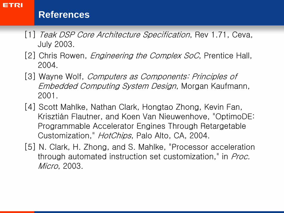
[1] Teak DSP Core Architecture Specification, Rev 1.71, Ceva, July 2003.
[2] Chris Rowen, Engineering the Complex SoC, Prentice Hall, 2004.
[3] Wayne Wolf, Computers as Components: Principles of Embedded Computing System Design, Morgan Kaufmann, 2001.
[4] Scott Mahlke, Nathan Clark, Hongtao Zhong, Kevin Fan, Krisztián Flautner, and Koen Van Nieuwenhove, "OptimoDE: Programmable Accelerator Engines Through RetargetableCustomization," HotChips, Palo Alto, CA, 2004.
[5] N. Clark, H. Zhong, and S. Mahlke, "Processor acceleration through automated instruction set customization," in Proc. Micro, 2003.